


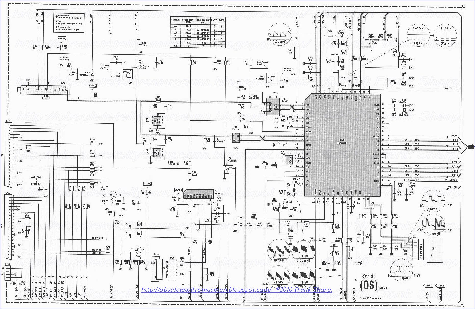
The THOMSON CHASSIS ICC17 was first and last THOMSON TV chassis featuring the PHILIPS TDA8855 and a complex circuitry all around the chassis.
The circuitry is complex even starting from the power supply and is an example on how complicate a TV chassis with lots of circuits and engineering solutions.
The THOMSON ICC17 was fitted in various formats of screen from 21 to 33 inches with slightly variants for the scope.
The features offered are great but the reliability wasn't excellent due to a line EHT trafo failing very often landing to a non functional TV and sometimes to a TDA8855 E/W output pin damaged.


THOMSON 28DG22C BLACKPEARL (413/ICC17EU) CHASSIS ICC17 Switched-mode power supply:
Switched-mode power supplies having a switching transistor (TP21), a driver stage (IP01) and an isolating transformer (TR1) which contains a primary winding (W1) and a secondary winding (W2), and in which a regulating signal is transmitted, for example via an optocoupler, from the secondary side to the primary side are known. The object of the present invention is to reduce the component complexity of these switched-mode power supplies, in particular for the transmission of this regulation information. The invention uses a secondary winding (W2) and four diodes (DS01, DS02, DS10, DS10) in order to produce two rectified positive voltages (US1, US2), one of which (US1) can be regulated. A connection of the unregulated voltage (US2) has connected to it a variable zener diode (IS10) as an error amplifier for transmitting a regulating signal to the primary side. The driver stage (IP01) provides a pulse-width-modulated square-wave signal for driving the switching transistor (TP21) which is arranged at high potential between the operating voltage (UB1) on the input side and the primary winding (W1). Arranged between the driver stage (IP01) and the control electrode of the switching transistor (TP21) there is a differentiating element (RP20, CP20) which produces positive and negative switching voltages for controlling the switching transistor (TP21). The base potential of the switching transistor (TP21) is connected via a resistor (RP21) to the operating voltage potential (UB1). The switched-mode power supply has very high efficiency, is very compact and is suitable, in particular, for use as a separate standby switched-mode power supply in entertainment electronic equipment.
Foreign References:
| DE3938172A1 | |||||||
| 5499175 | Power supply circuit | ||||||
| 5515256 | Self exciting type switching power supply circuit | ||||||
| 4885673 | Demagnetization monitoring device for a switching power supply with a primary and a secondary regulation | ||||||
| 5390100 | Freely oscillating switched-mode power supply | ||||||
| 4370701 | Energy conserving drive circuit for switched mode converter utilizing current snubber apparatus. |
 1. Switched-mode power supply having an isolating transformer (Tr1) which comprises a primary winding (W1) and a secondary winding (W2), and having a switching transistor (TP21), one end (5) of the secondary winding (W2) being connected to a rectifier diode (DS10), characterized in that a variable zener diode (IS10) is connected downstream from the diode (DS10).
 2. Switched-mode power supply according to Claim 1, characterized in that the variable zener diode is used as an error amplifier for regulating an output voltage (UE) of the switched-mode power supply, or any voltage of another switched-mode power supply.
3. Switched-mode power supply according to Claim 2, characterized in that the anode of the zener diode (IS10) is connected to earth and the control electrode is connected via a resistor network (RS10-RS13) to the output voltage (UE) to be stabilized.
4. Switched-mode power supply having an isolating transformer (Tr1) which comprises a primary winding (W1) and a secondary winding (W2), and having a switching transistor (TP21), characterized in that, at a first connection (5) of the secondary winding (W2), a diode (DS10) is connected in the forward direction to a first load (IS10), and a diode (DS01) is connected in the reverse direction to earth (GNDS) and, at a second connection (8) of the secondary winding (W2), a diode (DS20) is connected in the forward direction to a second load (IE) and a diode (DS02) is connected in the reverse direction to earth in order to produce two rectified, positive voltages (US1, US2) or, by reversing the polarity of the diodes (DS01, DS02, DS10, DS20), in order to produce two rectified, negative voltages.
5. Switched-mode power supply according to Claim 4, characterized in that one of the rectified voltages (US1, US2), which cannot be stabilized, can be used to stabilize another supply voltage, preferably by connection to a variable zener diode (IS10).
6. Switched
-mode power supply having an isolating transformer (Tr1) which comprises a primary winding (W1) and a secondary winding (W2), and having a switching transistor (TP21), a network containing a diode (DS20) and a capacitor (CS20) being connected to the secondary winding (W2) at a connection (8) in order to produce a smooth DC voltage (UE), characterized in that a light-emitting diode (BS20) is arranged in the forward direction between the diode (DS20) and the capacitor (CS20) in order to indicate the operating state. 7. Switched-mode power supply according to Claim 6, characterized in that the smooth DC voltage (UE) is used to supply a load having a low power consumption, preferably an infrared receiver.
8. Switched-mode power supply comprising a switching transistor (TP21), a driver stage (IP01), an isolating transformer (Tr1) with a primary winding (W1) and a secondary winding (W2) and an operating voltage (UB1) on the input side, the switching transistor (TP21) being arranged between the operating voltage (UB1) and the primary winding (W1), characterized in that the switching transistor (TP21) is driven by a differentiating element (RP20, CP20) arranged between the driver stage (IP01) and the switching transistor (TP21).
9. Switched-mode power supply according to Claim 8, characterized in that the differentiating element contains a resistor (RP20) and a capacitor (CP20) in series.
10. Switched-mode power supply according to Claim 9, characterized in that a resistor (RP21) is arranged between the operating voltage (UB1) and the base of the switching transistor (TP21).
11. Switched-mode power su
pply according to Claim 10, characterized in that the driver stage (IP01) produces square-wave pulses for driving the switching transistor (TP21), and in that the time constant of the differentiating element is chosen such that the differentiation of the square-wave pulses for controlling the switching transistor (TP21) produces suitable positive and negative pulses. 12. Switched-mode power supply according to Claim 11, characterized in that that end (4) of the primary winding (W1) which is at the lower potential is used to produce a supply voltage (UB2) on the primary side.
13. Switched-mode power supply according to Claim 12, characterized in that said switched-mode power supply contains a series circuit, which is connected to the operating voltage (UB1) and has two zener diodes (DP06, DP05), in order to stabilize the supply voltage (UB2).
14. Switched-mode power supply according to Claim 13, characterized in that the zener diode (DP05), which is connected to the operating voltage (UB1), is also used to provide the starting current for the driver stage (IP01).
15. Switched-mode power supply according to Claim 13, characterized in that the operating voltage (UB1) on the input side is a DC voltage whose magnitude is less than the AC voltage (VAC) on the input side.
Description:
The invention is based on a switched-mode power supply which contains a
 switching transistor as well as an isolating transformer having a primary winding and a secondary winding. These require a relatively high level of component complexity, particularly if regulation information must be transmitted from the secondary side to the primary side in order to stabilize an operating voltage on the secondary side. Various embodiments are known for transmitting this information, for example using an optocoupler. DE 40 04 707 discloses a circuit in which a regulating signal is transmitted back via a transistor stage in a brief time interval during a quiescent phase of the isolating transformer.
The object of the present invention is to reduce the component complexity for switched-mode power supplies of the type.
This object is achieved by the invention specified in Claims 1, 4, 6 and 8. Advantageous developments of the invention are specified in the subclaims.
According to the invention, a secondary winding is used to produce two rectified voltages of the same polarity by a suitable circuit of four diodes. As a result of this circuit, the switched-mode power supply operates both as a forward converter and as a flyback converter. Both voltages can therefore be used as operating voltages, although only one can be stabilized in a regulated switched-mode power supply. However, the other can advantageously be used for transmitting regulation information from the secondary side to the primary side. A variable zener diode which is used as an error amplifier, for example the Type TL 431, is particularly suitable for this purpose. This zener diode has a control input which is connected by means of a suitable circuit, via a passive resistor network, to a secondary voltage to be regulated.
Variation of the zener voltage of this zener diode allows the winding connected to it to be loaded to a greater or lesser extent so that this load can be tapped off via an auxiliary winding on the primary side of the isolating transformer.
 The stabilized operating voltage, which is preferably used for supplying a load having a low power consumption, contains a series-connected light-emitting diode to indicate operation of relevant equipment. Since the light-emitting diode is connected downstream from the rectifier diode and upstream of a stabilization capacitor, it is operated at the pulsating switching frequency of the switched-mode power supply. At the high switching frequencies used here, the light-emitting diode has a very low power consumption of only, for example, 3 milliwatts; there is therefore no need for any resistor in series with the light-emitting diode.
According to a development of the invention, the control input of the switching transistor is driven by the driver stage via a differentiating element, the switching transistor being arranged between the operating voltage on the input side and the primary winding of the isolating transformer. Since this results in the control input being DC-decoupled, it can be connected via a resistor to the potential of the operating voltage on the input side.
The driver stage produces square-wave pulses for driving the switching transistor. The time constant of the differentiating element is chosen such that the switching transistor is switched off by a positive pulse flank and is switched on by a negative pulse flank. The output voltage of the switched-mode power supply can be regulated by varying the pulse width and/or the frequency.
Since the switching transistor is connected upstream of the primary winding of the isolating transformer in the current flow direction, that end of the primary winding which is at the lower potential can be used to produce a supply voltage on the primary side. This can be stabilized by means of a network which contains two zener diodes and at the same time provides the starting current for the driver stage.
 The switched-mode power supply may have a very compact construction and, because of its low power consumption, is suitable in particular for use as a separate standby power supply for a television set or video recorder. In the standby mode, it drives, for example, only an infrared receiver and, for this purpose, requires a power consumption of less than 100 mW, including loads. This includes the light-emitting diode as an indication of operation, which is connected directly in the current path for supplying the infrared receiver.
Alternatively, the switched-mode power supply can advantageously be used to produce voltages with higher power levels, for example using further secondary windings, and one of these voltages can likewise be stabilized by means of the variable zener diode.
The invention will be explained in the following text using, by way of example, a schematic drawing in which the figure shows a circuit diagram of a switched-mode power supply designed according to the invention.
The switched-mode power supply in the figure contains a bridge rectifier having four diodes DP01 - DP04 for producing an operating voltage UB1 on the input side from an AC voltage VAC. The operating voltage UB1 is stabilized by two series-connected zener diodes DP05 and DP06 in parallel with two series-connected capacitors CP05 and CP06. A supply voltage UB2 is at the same time stabilized via the mutually connected centre tap of these series circuits. Two reactive elements C1 and C2 considerably reduce the AC voltage applied to the bridge rectifier. In this exemplary embodiment, the operating voltag e UB1 is 36 volts, and the supply voltage UB2 is 6 volts.
The operating voltage UB1 is connected to the emitter of a switching transistor TP21 whose collector is connected to the primary winding W1 of an isolating transformer Tr1. The second connection 4 of the primary winding W1, which is at a lower potential, is connected to the supply voltage UB2. The supply voltage UB2 is thus not only provided by the zener diode DP02 but is also obtained from the primary winding W1 by operation of the switching transistor TP21 and is stabilized by the zener diode DP06 and the capacitor CP06. The supply voltage UB2 is used to supply a driver stage IP01 and a transistor stage TP30.
In this exemplary embodiment, the driver stage IP01 is an oscillator in the form of an appropriately connected operational amplifier. It operates as an astable multivibrator and produces square-wave signals. The output of the driver stage IP01 is connected via a differentiating element to the control input of the switching transistor TP21. In this exemplary embodiment, the differentiating element comprises a series circuit formed by a resistor RP20and a capacitor CP20, whose values are chosen such that they differentiate the switching flanks of the oscillator signal.
Connected in parallel with the emitter and the base of the switching transistor TP21 there is a resistor RP21 which is used to draw the base potential of said switching transistor TP21 to the operating voltage UP1 so that the switching transistor is in the switched-off state when there is no drive signal. Differentiation of the square-wave pulses results in suitable positive and negative pulses being produced alternately in order to switch the switching transistor TP21 on and off.
The isolating transformer TR1 contains a primary auxiliary winding W3 which is used to provide a regulating signal for stabilizing one or more secondary output voltages. This regulating signal is amplified in a transistor stage TP30 and is supplied to the oscillator IP01 in order to regulate the pulse width and/or the frequency.
The switched-mode power supply operates, for example, at an oscillator frequency of 100 kHz, which is governed by the oscillator IP01. Alternatively, the switched-mode power supply can be synchronized, for example over a frequency range of 40 - 150 kHz. With appropriate component values, the differentiating element can be matched to the desired oscillation frequency or an oscillation range.
The following values were used for relevant components for the drive level illustrated in the figure: RP20 : 4.7 kOhm CP20 : 100 pF RP21 : 47 kOhm The switching transistor may also be, in particular, an MOS field-effect transistor which, because of its high-impedance gate input, can be controlled with very low switching currents.
The isolating transformer Tr1 of the switched-mode power supply contains one or possibly more secondary windings W2 for producing supply voltages. In this exemplary embodiment, a relatively small load IE, for example an infrared receiver of a television set or of a video recorder, is operated by means of a supply voltage US1.
The secondary winding W2 is connected to four diodes DS01, DS02, DS10 and DS20 in such a manner that two voltages of the same polarity are produced, in this case two positive voltages US1 and US2, in that, at a first connection 5 of the secondary winding W2, a diode DS10 is connected in the forward direction to a load IS10 and a diode DS01 is connected in the reverse direction to earth GNDS and, at a second connection 8 of the secondary winding W2, a diode DS20 is connected in the forward direction to the load IE and a diode DS02 is connected in the reverse direction to earth GNDS. Alternatively, two rectified, negative voltages can be produced by reversing the polarity of the diodes DS01, DS02, DS10, DS20.
The isolating transformer Tr1 DC-decouples the earth GNDS and the earth GNDP.
The voltage US1 is smoothed by a capacitor CS20 in order to supply the load IE with a stabilized output voltage UE. The supply voltage US2 is connected to the cathode of a variable zener diode IS10, its anode being at earth potential. The Type TL 431 zener diode from Motorola is particularly suitable for use as the variable zener diode IS10. The control electrode of this zener diode IS10 is connected via a resistor network RS10, RS11, RS12 and RS13 to a supply voltage to be stabilized, in this exemplary embodiment the voltage UE supplied to the load IE. Alternatively, by way of example, a supply voltage from a further secondary winding or from a further switched-mode power supply can be connected to the control electrode.
A light-emitting diode BS20 can advantageously be arranged in the forward direction between the diode DS20 and the capacitorCS20 in order to indicate the operating state. It is admittedly in the current path to a load but, since the load has only a low power consumption, this does not overload the light-emitting diode BS20. This saves any need for a series resistor. Since the light-emitting diode BS20 is arranged upstream of the smoothing capacitor CS20, it is operated by the voltage US1, which pulsates at the frequency of the switched-mode power supply. With this method of operation, it requires only a very small amount of power, in this exemplary embodiment only about 3 mW.
The switched-mode power supply in the figure produces the supply voltage US1 in the on phase and the supply voltage US2, of the same polarity, in the off phase, by means of the circuit which is used here and comprises the diodes DS01, DS02, DS10 and DS20. Thus, only one of the supply voltages US1, US2 can be stabilized if the pulse-width ratio and the frequency of the oscillator IP1 vary. However, the second supply voltage US2 can in this case advantageously be used to transmit regulation information from the secondary side to the primary side.
In this case, the variable zener diode IS10 replaces an error amplifier with complex circuitry. In addition, there is no need for any further secondary winding or any additional component, for example an optocoupler, to transmit the control information.
The resistors RS10 - RS14 of the resistor network via which the variable zener diode IS10 is connected to the output voltage UE to be stabilized have the following approximate values in this exemplary embodiment: RS10 : 330 K RS11 : 0 RS12 : 100 K RS13 : 100 K RS14 : 4.7 K
The exemplary embodiment in the figure is preferably used to produce low power levels on the secondary side and has very high efficiency. The transformer Tr1 may have a very compact design, particularly because it is designed only for a low operating voltage. The switched-mode power supply is therefore particularly suitable for use as a separate standby switched-mode power supply for entertainment electronic equipment. Alternatively, it can be designed for higher power levels, and is thus also suitable, for example, for use as a DC-DC converter in conjunction with a car battery. The switched-mode power supply is started in a simple manner via the zener diode DP05.
The switched-mode power supply has a transformer, a switching transistor (T1) connected in series with a primary winding (W1) of the transformer, a primary-side control circuit (DR) and a secondary-side regulating stage (SR). In this arrangement, the control circuit (DR) is used to drive the switching transistor (T1). The secondary-side regulating circuit (SR) is used to drive a coupling element (OK), which is used to transmit a regulating signal from the secondary side to the primary side. A first switch (T2) is situated between the control input of the switching transistor (T1) and a primary-side operating voltage (VCC), and a second switch (T4) is situated between the regulating stage (SR) and a secondary-side operating voltage (UB), with the two operating voltages (VCC, UB) being able to be disconnected using a single control signal (US). In this case, the isolating element (OK) transmits both the regulating information for the primary-side control circuit (DR) and the turn-off signal for the first switch (T2). If the second switch is turned off by the control signal, the regulating stage and the optocoupler become completely non-live and consume no further power. As a result of this, the optocoupler is off on the primary side, which means that the first switch is also turned off, so that both the switching transistor and the control circuit become non-live. In this situat
 ion, the switched-mode power supply is completely non-live except for the starting circuit, so that the power consumption can be reduced down to below 0.2 W in this state.

The object of the present invention is to reduce the component complexity for switched-mode power supplies of the type.
This object is achieved by the invention specified in Claims 1, 4, 6 and 8. Advantageous developments of the invention are specified in the subclaims.
According to the invention, a secondary winding is used to produce two rectified voltages of the same polarity by a suitable circuit of four diodes. As a result of this circuit, the switched-mode power supply operates both as a forward converter and as a flyback converter. Both voltages can therefore be used as operating voltages, although only one can be stabilized in a regulated switched-mode power supply. However, the other can advantageously be used for transmitting regulation information from the secondary side to the primary side. A variable zener diode which is used as an error amplifier, for example the Type TL 431, is particularly suitable for this purpose. This zener diode has a control input which is connected by means of a suitable circuit, via a passive resistor network, to a secondary voltage to be regulated.
Variation of the zener voltage of this zener diode allows the winding connected to it to be loaded to a greater or lesser extent so that this load can be tapped off via an auxiliary winding on the primary side of the isolating transformer.
The stabilized operating voltage, which is preferably used for supplying a load having a low power consumption, contains a series-connected light-emitting diode to indicate operation of relevant equipment. Since the light-emitting diode is connected downstream from the rectifier diode and upstream of a stabilization capacitor, it is operated at the pulsating switching frequency of the switched-mode power supply. At the high switching frequencies used here, the light-emitting diode has a very low power consumption of only, for example, 3 milliwatts; there is therefore no need for any resistor in series with the light-emitting diode.According to a development of the invention, the control input of the switching transistor is driven by the driver stage via a differentiating element, the switching transistor being arranged between the operating voltage on the input side and the primary winding of the isolating transformer. Since this results in the control input being DC-decoupled, it can be connected via a resistor to the potential of the operating voltage on the input side.
The driver stage produces square-wave pulses for driving the switching transistor. The time constant of the differentiating element is chosen such that the switching transistor is switched off by a positive pulse flank and is switched on by a negative pulse flank. The output voltage of the switched-mode power supply can be regulated by varying the pulse width and/or the frequency.
Since the switching transistor is connected upstream of the primary winding of the isolating transformer in the current flow direction, that end of the primary winding which is at the lower potential can be used to produce a supply voltage on the primary side. This can be stabilized by means of a network which contains two zener diodes and at the same time provides the starting current for the driver stage.
The switched-mode power supply may have a very compact construction and, because of its low power consumption, is suitable in particular for use as a separate standby power supply for a television set or video recorder. In the standby mode, it drives, for example, only an infrared receiver and, for this purpose, requires a power consumption of less than 100 mW, including loads. This includes the light-emitting diode as an indication of operation, which is connected directly in the current path for supplying the infrared receiver.Alternatively, the switched-mode power supply can advantageously be used to produce voltages with higher power levels, for example using further secondary windings, and one of these voltages can likewise be stabilized by means of the variable zener diode.
The invention will be explained in the following text using, by way of example, a schematic drawing in which the figure shows a circuit diagram of a switched-mode power supply designed according to the invention.
The switched-mode power supply in the figure contains a bridge rectifier having four diodes DP01 - DP04 for producing an operating voltage UB1 on the input side from an AC voltage VAC. The operating voltage UB1 is stabilized by two series-connected zener diodes DP05 and DP06 in parallel with two series-connected capacitors CP05 and CP06. A supply voltage UB2 is at the same time stabilized via the mutually connected centre tap of these series circuits. Two reactive elements C1 and C2 considerably reduce the AC voltage applied to the bridge rectifier. In this exemplary embodiment, the operating voltag
e UB1 is 36 volts, and the supply voltage UB2 is 6 volts.The operating voltage UB1 is connected to the emitter of a switching transistor TP21 whose collector is connected to the primary winding W1 of an isolating transformer Tr1. The second connection 4 of the primary winding W1, which is at a lower potential, is connected to the supply voltage UB2. The supply voltage UB2 is thus not only provided by the zener diode DP02 but is also obtained from the primary winding W1 by operation of the switching transistor TP21 and is stabilized by the zener diode DP06 and the capacitor CP06. The supply voltage UB2 is used to supply a driver stage IP01 and a transistor stage TP30.
In this exemplary embodiment, the driver stage IP01 is an oscillator in the form of an appropriately connected operational amplifier. It operates as an astable multivibrator and produces square-wave signals. The output of the driver stage IP01 is connected via a differentiating element to the control input of the switching transistor TP21. In this exemplary embodiment, the differentiating element comprises a series circuit formed by a resistor RP20
and a capacitor CP20, whose values are chosen such that they differentiate the switching flanks of the oscillator signal.Connected in parallel with the emitter and the base of the switching transistor TP21 there is a resistor RP21 which is used to draw the base potential of said switching transistor TP21 to the operating voltage UP1 so that the switching transistor is in the switched-off state when there is no drive signal. Differentiation of the square-wave pulses results in suitable positive and negative pulses being produced alternately in order to switch the switching transistor TP21 on and off.
The isolating transformer TR1 contains a primary auxiliary winding W3 which is used to provide a regulating signal for stabilizing one or more secondary output voltages. This regulating signal is amplified in a transistor stage TP30 and is supplied to the oscillator IP01 in order to regulate the pulse width and/or the frequency.
The switched-mode power supply operates, for example, at an oscillator frequency of 100 kHz, which is governed by the oscillator IP01. Alternatively, the switched-mode power supply can be synchronized, for example over a frequency range of 40 - 150 kHz. With appropriate component values, the differentiating element can be matched to the desired oscillation frequency or an oscillation range.
The following values were used for relevant components for the drive level illustrated in the figure: RP20 : 4.7 kOhm CP20 : 100 pF RP21 : 47 kOhm The switching transistor may also be, in particular, an
MOS field-effect transistor which, because of its high-impedance gate input, can be controlled with very low switching currents.The isolating transformer Tr1 of the switched-mode power supply contains one or possibly more secondary windings W2 for producing supply voltages. In this exemplary embodiment, a relatively small load IE, for example an infrared receiver of a television set or of a video recorder, is operated by means of a supply voltage US1.
The secondary winding W2 is connected to four diodes DS01, DS02, DS10 and DS20 in such a manner that two voltages of the same polarity are produced, in this case two positive voltages US1 and US2, in that, at a first connection 5 of the secondary winding W2, a diode DS10 is connected in the forward direction to a load IS10 and a diode DS01 is connected in the reverse direction to earth GNDS and, at a second connection 8 of the secondary winding W2, a diode DS20 is connected in the forward direction to the load IE and a diode DS02 is connected in the reverse direction to earth GNDS. Alternatively, two rectified, negative voltages can be produced by reversing the polarity of the diodes DS01, DS02, DS10, DS20.
The isolating transformer Tr1 DC-decouples the earth GNDS and the earth GNDP.
The voltage US1 is smoothed by a capacitor CS20 in order to supply the load IE with a stabilized output voltage UE. The supply voltage US2 is connected to the cathode of a variable zener diode IS10, its anode being at earth potential. The Type TL 431 zener diode from Motorola is particularly suitable for use as the variable zener diode IS10. The control electrode of this zener diode IS10 is connected via a resistor network RS10, RS11, RS12 and RS13 to a supply voltage to be stabilized, in this exemplary embodiment the voltage UE supplied to the load IE. Alternatively, by way of example, a supply voltage from a further secondary winding or from a further switched-mode power supply can be connected to the control electrode.
A light-emitting diode BS20 can advantageously be arranged in the forward direction between the diode DS20 and the capacitor
CS20 in order to indicate the operating state. It is admittedly in the current path to a load but, since the load has only a low power consumption, this does not overload the light-emitting diode BS20. This saves any need for a series resistor. Since the light-emitting diode BS20 is arranged upstream of the smoothing capacitor CS20, it is operated by the voltage US1, which pulsates at the frequency of the switched-mode power supply. With this method of operation, it requires only a very small amount of power, in this exemplary embodiment only about 3 mW.The switched-mode power supply in the figure produces the supply voltage US1 in the on phase and the supply voltage US2, of the same polarity, in the off phase, by means of the circuit which is used here and comprises the diodes DS01, DS02, DS10 and DS20. Thus, only one of the supply voltages US1, US2 can be stabilized if the pulse-width ratio and the frequency of the oscillator IP1 vary. However, the second supply voltage US2 can in this case advantageously be used to transmit regulation information from the secondary side to the primary side.
In this case, the variable zener diode IS10 replaces an error amplifier with complex circuitry. In addition, there is no need for any further secondary winding or any additional component, for example an optocoupler, to transmit the control information.
The resistors RS10 - RS14 of the resistor network via which the variable zener diode IS10 is connected to the output voltage UE to be stabilized have the following approximate values in this exemplary embodiment: RS10 : 330 K RS11 : 0 RS12 : 100 K RS1
3 : 100 K RS14 : 4.7 KThe exemplary embodiment in the figure is preferably used to produce low power levels on the secondary side and has very high efficiency. The transformer Tr1 may have a very compact design, particularly because it is designed only for a low operating voltage. The switched-mode power supply is therefore particularly suitable for use as a separate standby switched-mode power supply for entertainment electronic equipment. Alternatively, it can be designed for higher power levels, and is thus also suitable, for example, for use as a DC-DC converter in conjunction with a car battery. The switched-mode power supply is started in a simple manner via the zener diode DP05.

1. Switched-mode power supply having a transformer, a switching transistor (T1) in series with a primary winding (W1) of the transformer, a primary-side control circuit (DR) and having a secondary-side regulating stage (SR), characterized in that a control input of the switching transistor (T1) is connected to a first switch (T2), and there is a second switch (T4) between the regulating stage (SR) and an operating voltage (UB), and in that the turning-off of the second switch (T4) simultaneously causes the first switch (T2) to be turned off.
2. Switched-mode power supply according to Claim 1, characterized in that the regulating stage (SR) is connected via a coupling element (OK) both to the control circuit (DR) and to the first switch (T2).
3. Switched-mode power supply according to Claim 1 or 2, characterized in that the regulating stage (SR) has a transistor stage (T3, R8, R9, D6) whose connections are connected to an output voltage of the switched-mode power supply (UA), to the coupling element (OK) and to the second switch (T4) in order to transmit both a regulating signal and a control signal (US).
4. Switched-mode power supply according to Claim 2 or 3, characterized in that a control signal (US) can be used to turn off the second switch (T4), so that the supply voltage (UB) for the regulating stage (SR) is disconnected, and this turns off the first switch (T2) via the coupling element (OK).
5. Switched-mode power supply according to one of the preceding claims, characterized in that the first switch (T2) is situated between the control input of the switching transistor (T1) and a primary-side operating voltage (VCC).
6. Switched-mode power supply according to one of the preceding claims, characterized in that, on the primary side, one connection (2) of the coupling element (OK) is connected to an auxiliary winding (W2b) of the transformer, and another connection (1) of the coupling element (OK) is connected both to the first switch (T2) and to the control circuit (DR).
7. Switched-mode power supply according to Claim 6, characterized in that a diode (D1) is arranged between the control circuit (DR) and the coupling element (OK) and also the first switch (T2).
8. Switched-mode power supply according to Claim 5, 6 or 7, characterized in that the control input of the first switch (T2) is connected to the primary-side operating voltage (VCC) via a resistor (R4), which produces a high voltage on this control input in order to turn off the switch (T2) when the coupling element (OK) has a high impedance.
9. Switched-mode power supply according to one of the preceding claims 2 - 8, characterized in that the coupling element (OK) is an optocoupler, an emitter connection (2) of which on the primary side is connected to a flyback negative winding (W2b), so that the switched-mode power supply starts softly when it is turned on.
10. Switched -mode power supply according to one of the preceding claims, characterized in that the secondary-side operating voltage (UB) is produced by another power supply unit, and in that the switched-mode power supply is used as an additional power supply unit which can be fully disconnected and reconnected by means of the control signal (US).
2. Switched-mode power supply according to Claim 1, characterized in that the regulating stage (SR) is connected via a coupling element (OK) both to the control circuit (DR) and to the first switch (T2).
3. Switched-mode power supply according to Claim 1 or 2, characterized in that the regulating stage (SR) has a transistor stage (T3, R8, R9, D6) whose connections are connected to an output voltage of the switched-mode power supply (UA), to the coupling element (OK) and to the second switch (T4) in order to transmit both a regulating signal and a control signal (US).
4. Switched-mode power supply according to Claim 2 or 3, characterized in that a control signal (US) can be used to turn off the second switch (T4), so that the supply voltage (UB) for the regulating stage (SR) is disconnected, and this turns off the first switch (T2) via the coupling element (OK).
5. Switched-mode power supply according to one of the preceding claims, characterized in that the first switch (T2) is situated between the control
input of the switching transistor (T1) and a primary-side operating voltage (VCC). 6. Switched-mode power supply according to one of the preceding claims, characterized in that, on the primary side, one connection (2) of the coupling element (OK) is connected to an auxiliary winding (W2b) of the transformer, and another connection (1) of the coupling element (OK) is connected both to the first switch (T2) and to the control circuit (DR).
7. Switched-mode power supply according to Claim 6, characterized in that a diode (D1) is arranged between the control circuit (DR) and the coupling element (OK) and also the first switch (T2).
8. Switche
d-mode power supply according to Claim 5, 6 or 7, characterized in that the control input of the first switch (T2) is connected to the primary-side operating voltage (VCC) via a resistor (R4), which produces a high voltage on this control input in order to turn off the switch (T2) when the coupling element (OK) has a high impedance. 9. Switched-mode power supply according to one of the preceding claims 2 - 8, characterized in that the coupling element (OK) is an optocoupler, an emitter connection (2) of which on the primary side is connected to a flyback negative winding (W2b), so that the switched-mode power supply starts softly when it is turned on.
10. Switched
-mode power supply according to one of the preceding claims, characterized in that the secondary-side operating voltage (UB) is produced by another power supply unit, and in that the switched-mode power supply is used as an additional power supply unit which can be fully disconnected and reconnected by means of the control signal (US).
Description:
The present invention relates to a switched-mode power supply having a transformer, a switching transistor connected in series with a primary winding of the transformer, a control circuit and a secondary-side regulating stage. Switched-mode power supplies of this type are used in appliances for consumer electronics, for example.
To be able to turn appliances having a switched-mode power supply on and off using a remote control, it is necessary to keep them in a constant standby mode in order to turn them on. However, this means that the switched-mode power supply is constantly consuming power. To keep the power consumption of the switched-mode power supply as low as possible in standby operation, switched-mode power supplies with a burst mode have been developed, for example, or a separate power supply unit is used just for standby operation. EP-A 0 803 966 discloses a power supply unit, for example, in which a relatively large switched-mode power supply is used just for normal operation and a smaller switched-mode power supply is used for standby operation.
In this arrangement, the two switched-mode power supplies are coupled to one another such that the larger switched-mode power supply is regulated by means of the small switched-mode power supply during normal operation, and the small switched-mode power supply oscillates using a dedicated oscillator in standby operation.
The invention is based on the object of specifying a switched-mode power supply of the type mentioned in the introduction which has a very low power consumption.
This object is achieved by the features specified in Claim 1. Advantageous developments of the invention are specified in the subclaims.
The switched-mode power supply of the invention has a transformer, a switching transistor connected in series with a primary winding of the transformer, a primary-side control circuit and a secondary-side regulating stage. In this arrangement, the control circuit is used to drive the switching transistor. The secondary-side regulating circuit is used to drive a coupling element, which is used to transmit a regulating signal from the secondary to the primary. A first switch is situated between the control input of the switching transistor and a primary-side operating voltage, and a second switch is situated between the regulating stage and a secondary-side operating voltage, with the two operating voltages being able to be disconnected by means of the two switches using a single control signal.
In this case, the isolating element transmits both the regulating information for the primary-side control circuit and the turn-off signal for the first switch.
In this case, the control signal for turning off the two switches is applied to a control input of the second switch, and, when this switch is off, the secondary-side regulating stage is disconnected at the same time and the first switch is turned off via the coupling element. The coupling element is preferably an optocoupler driven on the secondary side by a transistor stage of the secondary-side regulating stage, at which both the switched-mode power supply's output voltage which is to be regulated and, via the second switch, the control signal information are present.
If the second switch is turned off by the control signal, the regulating stage and the optocoupler become completely non-live and consume no further power. As a result of this, the optocoupler is off on the primary side, which means that the first switch is also turned off, so that both the switching transistor and the control circuit become non-live. In this situation, the switched-mode power supply is completely non-live except for the starting circuit, so that the power consumption is below 0.2 W in this state.
The invention is explained in more detail below with reference to a schematic circuit diagram, in which: the figure shows a switched-mode power supply, according to the invention, having primary-side and secondary-side circuitry.
The figure shows, on the primary side, a switching transistor T1 in series with a primary winding W1 of a transformer. For the purposes of simpler illustration, the transformer is not shown in the figure; as is usual with appliances in entertainment electronics, it is designed with power supply isolation and, apart from the primary winding W1, contains one or more primary windings for operation of the switched-mode power supply, and, on the secondary, one or more windings for providing the required output voltages.
In this illustrative embodiment, the transistor T1 is a MOSFET controlled by a control circuit DR. The primary-side auxiliary winding W2a is used to provide an operating voltage VCC which is rectified via a diode D2 and is buffered by a capacitor C1. A starting circuit A, which establishes a connection to the power supply rectifier or to a DC voltage produced from the power supply via a high-value resistor chain in a manner which is known, is used to provide the current necessary for starting the switched-mode power supply. Connected in parallel with the capacitor C1 is a zener diode D3, which limits the operating voltage VCC.
On the secondary side, the figure shows a winding W3 which, via a diode D5 and a capacitor C3, produces an output voltage UA which is to be stabilized. This output voltage UA is tapped off across a resistor R7 by a secondary-side regulating stage SR and is conditioned for transmission to the primary side. Transmission is effected by a coupling element, which is an optocoupler OK in this illustrative embodiment. Other coupling elements, such as transformers, can likewise be used. On the primary side, the regulating signal transmitted by the regulating stage SR via the optocoupler OK is applied to the control circuit DR, which converts this signal into a pulse-width-modulated control voltage U2 for driving the switching transistor T1.
The control circuit DR also uses another voltage U1 for driving, said voltage being applied across a resistor R3 and being an indication of the current flowing through the switching transistor T1.
The switched-mode power supply can be designed both as a free-running switched-mode power supply which changes its switching frequency depending on the load, and as a switched-mode power supply operating with pulse-width modulation at a fixed switching frequency. A switched-mode power supply of this type is specified in EP 0 808 015 A2, for example. In this case, the regulation is frequently applied to a secondary-side output voltage, since this allows better stabilization of the output voltage.
Between the operating voltage VCC and the control input of the switching transistor T1 there is a resistor R1 in order to allow the control voltage U2 to be decoupled from the control circuit DR and the operating voltage VCC. In this connection between the switching transistor T1 and the operating voltage VCC there is a first switch T2, in this illustrative embodiment a transistor, which can turn off the operating voltage VCC. The control input of this switch is connected via resistors R5 and R6 to the optocoupler OK, which can be used to drive the switch T2 from the secondary side. If the optocoupler OK has a high impedance on the primary side, then the operating voltage VCC is applied to the control input of the first switch T2 via a resistor R4, so that no current can flow via the emitter-base junction of the transistor T2, which means that the latter is off.
If a low voltage is applied to the control input of the switch T2, then the latter turns on. The control circuit DR is likewise connected to the optocoupler OK via a diode D1 and the resistor R6, so that said optocoupler transmits both the secondary-side regulating information and the turn-off signal for the first switch T2.
On the secondary side, the optocoupler contains a light-emitting diode operated via connections 3 and 4. This diode is driven by a transistor stage having a transistor T3 controlling the current through the light-emitting diode in the optocoupler, a secondary-side operating voltage UB being applied to the connection 3 of the optocoupler via a second switch T4. The control input of the transistor T3 has a constant voltage applied to it which is formed by a voltage divider which contains a resistor R9 and a zener diode D6 and which has the operating voltage UB across it during operation.
Via a voltage divider formed from the resistors R7 and R8, the emitter of the transistor T3 is at the output voltage UA to be regulated, so that the current through the light-emitting diode of the optocoupler OK is controlled via the base-emitter junction of the transistor T3 as a function of the output voltage UA. Instead of this transistor stage having the transistor T3, a variable zener diode can also be used for transmitting the regulating signal.
The second switch T4 is turned on and off via a transistor stage T5 having resistors R11, R12 by a control signal US from a digital circuit. If the control signal US is "zero", then transistor T5 is off, which means that the transistor T4 is also off, because its control input is in this case at a high potential via the resistor R10.
If the switch T4 is off, then neither the transistor stage having the transistor T3 nor the light-emitting diode in the optocoupler OK are live. This means that the photoresistance of the optocoupler OK is also high, so that the first switch T2 is likewise off, as described above. In this case, the control circuit DR also switches off, since no more current flows through the diode D1.
The regulating transmission via the optocoupler OK is carried out so that, when the output voltage UA is too high, the output of the optocoupler OK, connections 1 and 2, has a relatively high impedance, and, when the output voltage UA is too low, it has a relatively low impedance. The MOSFET used as a switching transistor is off at a control voltage U2 of below approximately 2 volts. The control circuit DR is likewise decoupled from the operating voltage VCC by the diode D1. If the control signal US is zero, therefore, then neither the secondary-side switching stages having the transistors T3, T4 and T5 nor the transistors T1 and T2 and the primary-side control circuit DR are live. When the switched-mode power supply is in the turned-off state, this means that only the starting circuit A consumes a very small amount of power.
The connection 2 of the optocoupler OK is connected to a flyback negative winding W2b via a diode D4, so that the switched-mode power supply starts softly when it is turned on. In the switched-mode power supply's starting phase, the negative voltage present on the winding W2b during the turned-off phase of the switching transistor T1 is still relatively low, so that the regulating signal transmitted via the optocoupler OK is attenuated. Only in normal operation, when the flyback negative voltage has developed on the winding W2b and the capacitor C2 is charged to a corresponding negative voltage, does the regulating signal become active at full strength for the control circuit DR.
A switched-mode power supply of this type can beused, in particular, in appliances for consumer electronics, and allows the power consumption to be kept very low in standby operation. In these appliances, flyback converters are predominantly used as the power supply unit, but the invention can also be used for other types of switched-mode power supplies. However, the second operating voltage UB must always be present in order to turn on the switched-mode power supply. This operating voltage can be provided by a second power supply unit, for example, or by a battery or a rechargeable battery.
A switched mode power supply (SMPS) as commonly used in consumer devices as television receivers, video recorders and audio equipment, is operated alternatively in a normal operating mode or in a standby mode wit h reduced or switched off operating voltages. Furthermore such a SMPS usually is provided with a protection circuit for the event of a short-circuit or an overloading or any other failure. Such a SMPS with a standby circuit and a protection circuit often exhibits a high complexity with a high number of components also reducing the reliability of the SMPS. It is an object to decrease the complexity and the number of components needed and thereby to improve the reliability of the SMPS. The switched mode power supply comprises a power switching transistor in series with the primary winding of a transformer and a further transistor (TP025) arranged at the primary side of the power supply, and further a standby control circuit arranged at the secondary side and coupled to said further transistor (TP025) for swi
 tching to stand-by mode in response to a standby switching signal (Us). The SMPS is further provided with a protection circuit (4) having an output terminal (b) coupled to the standby control circuit for actuating also said transistor (TP025) in the event of a fault and having a control input terminal (a) connected to different output voltages (UB2) which are generated by the switched mode power supply unit.
 THOMSON 28DG22C BLACKPEARL (413/ICC17EU) CHASSIS ICC17 Automatic degaussing circuit with switch mode power supply:
A degaussing circuit for a color television receiver has a continuously energized switch mode power supply feeding a voltage doubler coupled to a resonating capacitor connected in series with a degaussing coil for charging the capacitor while the receiver is off. A triac connects the capacitor and the degaussing coil in parallel when the television receiver low voltage on/off switch is turned on.
1. A color television receiver comprising:
a continuously energized switch mode power supply having a high voltage terminal and a low voltage terminal;
low voltage switch coupled to the low voltage terminal of said power supply for turning said receiver on and off; voltage multiplier means connected to the high voltage terminal;
degaussing means, including a picture tube degaussing coil and a resonating capacitor, connected to said power supply, said resonating capacitor being connected to said multiplier output and charged from said power supply to a voltage higher than that at said high voltage terminal when said receiver is off; and
electronic switch means including an energizing terminal coupled to said low voltage switch, said switch electrically connecting said resonating capacitor in parallel with said degaussing coil for producing a degaussing current therein whenever said receiver is turned on.
2. A television receiver as set forth in claim 1 wherein said electronic switch means comprises a bidirectional switching triac.
3. A television receiver as set forth in claim 3 wherein said receiver includes a horizontal output circuit coupled to said high voltage terminal, a horizontal drive circuit coupled to said low voltage switch and voltage increasing means AC coupled between said high voltage terminal and said degaussing means for producing said higher voltage for said degaussing means.
4. A television receiver as set forth in claim 3, further including; a large resistance connected between said power supply and said triac for minimizing current flow in said triac when said receiver is on.
5. A television receiver as set forth in claim 4 wherein said switch mode power supply includes a transformer winding coupled to said high voltage terminal and wherein said voltage increasing means comprise: an overwinding on said transformer winding, said connecting means being coupled to said overwinding rather than to said high voltage terminal.
6. A television receiver as set forth in claim 4 wherein said voltage increasing means comprise a voltage doubler arrangement.
7. A color television receiver comprising: a continuously energized switch mode power supply having a high voltage terminal and a low voltage terminal;
a low voltage switch coupled to said low voltage terminal for turning said receiver on and off;
degaussing means, including a picture tube degaussing coil and a resonating capacitor, coupled to said high voltage terminal, said resonating capacitor being normally connected to the high voltage terminal and thereby charged from said power supply when said receiver is off;
a triac switch electrically connecting said resonating capacitor in parallel with said degaussing coil for producing a degaussing current therein whenever said receiver is turned on, said triac switch including a gate electrode energized from closure of said low voltage switch; and
voltage multiplier means coupled to said switch mode power supply for producing a still higher voltage for application to said degaussing means.
8. A television receiver as set forth in claim 7 wherein said voltage increasing means includes a voltage doubler coupled to said high voltage terminal.
9. A television receiver as set forth in claim 7 wherein said switch mode power supply includes a transformer winding coupled to said high voltage terminal and wherein said voltage increasing means comprise an overwinding on said transformer winding for providing a higher voltage.
PHILIPS TDA8351 DC-coupled vertical deflection circuit:
FEATURES
• Few external components
• Highly efficient fully DC-coupled vertical output bridge
circuit
• Vertical flyback switch
• Guard circuit
• Protection against:
– short-circuit of the output pins (7 and 4)
– short-circuit of the output pins to VP
• Temperature protection
• High EMC immunity because of common mode inputs
• A guard signal in zoom mode.
GENERAL DESCRIPTION
The TDA8351 is a power circuit for use in 90° and 110°
colour deflection systems for field frequencies of 50 to
120 Hz. The circuit provides a DC driven vertical
deflection output circuit, operating as a highly efficient
class G system.
Note
1.
A flybac
(depending on IO and the inductance of the coil) has to be connected between pin 7 and ground. The decoupling
capacitor of VFB has to be connected between pin 6 and pin 3. This supply voltage line must have a resistance of
33 Ω.
 k supply voltage of >50 V up to 60 V is allowed in application. A 220 nF capacitor in series with a 22 Ω resistor
FUNCTIONAL DESCRIPTION
The vertical driver circuit is a bridge configuration. The
deflectioncoilisconnectedbetweentheoutputamplifiers,
which are driven in opposite phase. An external resistor
(RM) connected in series with the deflection coil provides
internal feedback information. The differential input circuit
is voltage driven. The input circuit has been adapted to
enable it to be used with the TDA9150, TDA9151B,
TDA9160A, TDA9162, TDA8366 and TDA8376 which
deliver symmetrical current signals. An external resistor
(RCON) connected between the differential input
determines the output current through the deflection coil.
Therelationshipbetweenthedifferentialinputcurrentand
the output current is defined by: Idiff× RCON= Icoil× RM.
The output current is adjustable from 0.5 A (p-p) to 3 A
(p-p) by varying RM. The maximum input differential
voltage is 1.8 V. In the application it is recommended that
Vdiff= 1.5 V (typ). This is recommended because of the
spread of input current and the spread in the value of
RCON.
The flyback voltage is determined by an additional supply
voltage VFB. The principle of operating with two supply
voltages (class G) makes it possible to fix the supply
voltage VPoptimum for the scan voltage and the second
supply voltage VFBoptimum for the flyback voltage. Using
this method, very high efficiency is achieved.
The supply voltage VFB is almost totally available as
flyback voltage across the coil, this being possible due to
the absence of a decoupling capacitor (not necessary,
due to the bridge configuration). Built-in protections are:
• thermal protection
• short-circuit protection of the output pins (pins 4 and 7)
• short-circuit protection of the output pins to VP.
A guard circuit VO(guard) is provided. The guard circuit is
activated at the following conditions:
• during flyback
• during short-circuit of the coil and during short-circuit of
the output pins (pins 4 and 7) to VP or ground
• during open loop
• when the thermal protection is activated.
This signal can be used for blanking the picture tube
screen.Notes
1.
A flyback supply voltage of >50 V up to 60 V is allowed in application. A 220 nF capacitor in series with a 22 Ω resistor
(dependent on IO and the inductance of the coil) has to be connected between pin 7 and ground. The decoupling
capacitor of VFB has to be connected between pin 6 and pin 3. This supply voltage line must have a resistance of
33 Ω
2.
The linearity error is measured without S-correction and based on the same measurement principle as performed on
the screen. The measuring method is as follows:
Divide the output signal I4− I7(VRM) into 22 equal parts ranging from 1 to 22 inclusive. Measure the value of two
succeeding parts called one block starting with part 2 and 3 (block 1) and ending with part 20 and 21 (block 10). Thus
part 1 and 22 are unused. The equations for linearity error for adjacent blocks (LEAB) and linearity error for not
adjacent blocks (LENAB) are given below:
;
3.
Referenced to VP.
4.
The V values within formulae relate to voltages at or across relative pin numbers, i.e. V7-4/V1-2= voltage value across
pins 7 and 4 divided by voltage value across pins 1 and 2.
5.
V9-4 AC short-circuited.
6.
Frequency response V7-4/V9-4 is equal to frequency response V7-4/V1-2.
7.
At V(ripple)= 500 mV eff; measured across RM; fi= 50 Hz.
PHILIPS TDA6107Q Triple video output amplifier :
GENERAL DESCRIPTION
The TDA6107Q includes three video output amplifiers in
one plastic DIL-bent-SIL 9-pin medium power (DBS9MPF)
package (SOT111-1), using high-voltage DMOS
technology, and is intended to drive the three cathodes of
a colour CRT directly. To obtain maximum performance,
the amplifier should be used with black-current control.
FEATURES
· Typical bandwidth of 5.5 MHz for an output signal of
60 V (peak-to-peak
 value)
· High slew rate of 900 V/ms
· No external components required
· Very simple application
· Single supply voltage of 200 V
 · Internal reference voltage of 2.5 V
· Fixed gain of 50.
TDA6107 PINNING
SYMBOL PIN DESCRIPTION
Vi(1) 1 inverting input 1
Vi(2) 2 inverting input 2
Vi(3) 3 inverting input 3
GND 4 ground (fin)
Iom 5 black current measurement output
VDD 6 supply voltage
Voc(3) 7 cathode output 3
Voc(2) 8 cathode output 2
Voc(1) 9 cathode output 1
HANDLING
Inputs and outputs are protected against electrostatic discharge in normal handling. However, to be totally safe, it is
desirable to take normal precautions appropriate to handling MOS devices (see “Handling MOS Devices”).

THOMSON 28DG22C BLACKPEARL (413/ICC17EU) CHASSIS ICC17 - Main CPU CCU ST92R195A9Q0/JAL (THOMSON) ROMLESS HCMOS MCU WITH
ON-SCREEN-DISPLAY AND TELETEXT DATA SLICER.
GENERAL DESCRIPTION
1.1 INTRODUCTION
The ST92R195B microcontroller is developed and
manufactured by STMicroelectronics using a proprietary
n-well HCMOS process. Its performance
derives from the use of a flexible 256-register programming
model for ultra-fast context switching
and real-time event response. The intelligent onchip
peripherals offload the ST9 core from I/O and
data management processing tasks allowing critical
application tasks to get the maximum use of
c
 ore resources. The ST92R195B MCU supports
low power consumption and low voltage operation
for power-efficient and low-cost embedded systems.
1.1.1 ST9+ Core
The advanced Core consists of the Central
Processing Unit (CPU), the Register File and the
Interrupt controller.
The general-purpose registers can be used as accumulators,
index registers, or address pointers.
Adjacent register pairs make up 16-bit registers for
addressing or 16-bit processing. Although the ST9
has an 8-bit ALU, the chip handles 16-bit operations,
including arithmetic, loads/stores, and memory/
register and memory/memory exchanges.
Two basic addressable spaces are available: the
Memory space and the Register File, which includes
the control and status registers of the onchip
peripherals.
1.1.2 Power Saving Modes
To optimize performance versus power consumption,
a range of operating modes can be dynamically
selected.
Run Mode. This is the full speed execution mode
with CPU and peripherals running at the maximum
clock speed delivered by the Phase Locked Loop
(PLL) of the Clock Control Unit (CCU).
Wait For Interrupt Mode. The Wait For Interrupt
(WFI) instruction suspends program execution until
an interrupt request is acknowledged. During
WFI, the CPU clock is halted while the peripheral
and interrupt controller keep running at a frequency
programmable via the CCU. In this mode, the
power consumption of the device can be reduced
by more than 95% (LP WFI).
Halt Mode. When executing the HALT instruction,
and if the Watchdog is not enabled, the CPU and
its peripherals stop operating and the status of the
machine remains frozen (the clock is also
stopped). A reset is necessary to exit from Halt
mode.
1.1.3 I/O Ports
Up to 23 I/O lines are dedicated to digital Input/
Output. These lines are grouped into up to five I/O
Ports and can be configured on a bit basis under
software control to provide timing, status signals,
timer and output, analog inputs, external interrupts
and serial or parallel I/O.
1.1.4 TV Peripherals
A set of on-chip peripherals form a complete system
for TV set and VCR applications:
– Voltage Synthesis
– VPS/WSS Slicer
– Teletext Slicer
– Teletext Display RAM
– OSD
1.1.5 On Screen Display
The human interface is provided by the On Screen
Display module, this can produce up to 26 lines of
up to 80 characters from a ROM defined 512 character
set. The character resolution is 10x10 dots.
Four character sizes are supported. Serial attributes
allow the user to select foreground and
background colours, character size and fringe
background. Parallel attributes can be used to select
additional foreground and background colors
and underline on a character by character basis.
1.1.6 Teletext and Display RAM
The internal 8k Teletext and Display storage RAM
can be used to store Teletext pages as well as Display
parameters.
THOMSON 28DG22C BLACKPEARL (413/ICC17EU) CHASSIS ICC17 PHILIPS TDA8855H I2C-bus controlled PAL/NTSC/SECAM TV processor:GENERAL DESCRIPTION:
The various versions of the TDA 884X/5X series are
I2C-bus controlled single chip TV processors which are
intended to be applied in PAL, NTSC, PAL/NTSC and
multi-standard television receivers. The N2 version is pin
and application compatible with the N1 version, however,
a new feature has been added which makes the N2 more
attractive. The IF PLL demodulator has been replaced by
an alignment-free IF PLL demodulator with internal VCO
(no tuned circuit required). The setting of the various
frequencies (33.4, 33.9, 38, 38.9, 45,75 and 58.75 MHz)
can be made via the I2C-bus.
Because of this difference the N2 version is compatible
with the N1, however, N1 devices cannot be used in an
optimised N2 application.
Functionally the IC series is split up is 3 categories, viz:
· Versions intended to be used in economy TV receivers
with all basic functions (envelope: S-DIP 56 and QFP
64)
· Versions wit h additional features like E-W geometry
control, H-V zoom function and YUV interface which are
intended for TV receivers with 110° picture tubes
(envelope: S-DIP 56)
· Versions which have in addition a second RGB input
with saturation control and a second CVBS output
(envelope: QFP 64)
FUNCTIONAL DESCRIPTION
Vision IF amplifier
The IF-amplifier contains 3 ac-coupled control stages with
a total gain control range which is higher then 66 dB. The
sensitivity of the circuit is comparable with that of modern
IF-IC’s.
The video signal is demodulated by means of an
alignment-free PLL carrier regenerator with an internal
VCO. This VCO is calibrated by means of a digital control
circuit which uses the X-tal frequency of the colour
decoder as a reference. The frequency setting for the
various standards (33.4, 33.9, 38, 38.9, 45.75 and 58.75
MHz) is realised via the I2C-bus. To get a good
performance for phase modulated carrier signals the
control speed of the PLL can be increased by means of the
FFI bit.
The AFC output is generated by the digital control circuit of
the IF-PLL demodulator and can be read via the I2C-bus.
For fast search tuning systems the window of the AFC can
be increased with a factor 3. The setting is realised with the
AFW bit. The AFC data is valid only when the horizontal
PLL is in lock (SL = 1)
Depending on the type the AGC-detector operates on
top-sync level (single standard versions) or on top sync
and top white- level (multi standard versions). The
demodulation polarity is switched via the I2C-bus. The
AGC detector time-constant capacitor is connected
externally. This mainly because of the flexibility of the
application. The time-constant of the AGC system during
positive modulation is rather long to avoid visible variations
of the signal amplitude. To improve the speed of the AGC
system a circuit has been included which detects whether
the AGC detector is activated every frame period. When
during 3 field periods no action is detected the speed of the
system is increased. For signals without peak white
information the system switches automatically to a gated
black level AGC. Because a black level clamp pulse is
required for this way of operation the circuit will only switch
to black level AGC in the internal mode.
The circuits contain a video identification circuit which is
independent of the synchronisation circuit. Therefore
search tuning is possible when the display section of the
receiver is used as a monitor. However, this ident circuit
cannot be made as sensitive as the slower sync ident
circuit (SL) and we recommend to use both ident outputs
to obtain a reliable search system. The ident output is
supplied to the tuning system via the I2C-bus.
The input of the identification circuit is connected to pin 13
(S-DIP 56 devices), the “internal” CVBS input (see Fig.6).
This has the advantage that the ident circuit can also be
made operative when a scrambled signal is received
(descrambler connected between pin 6 (IF video output)
and pin 13). A second advantage is that the ident circuit
can be used when the IF amplifier is not used (e.g. with
built-in satellite tuners).
The video ident circuit can also be used to identify the
selected CBVS or Y/C signal. The switching between the
2 modes can be realised with the VIM bit.
Video switches
The circuits have two CVBS inputs (internal and external
CVBS) and a Y/C input. When the Y/C input is not required
the Y input can be used as third CVBS input. The switch
configuration is given in Fig.6. The selection of the various
sources is made via the I2C-bus.
For the TDA 884X devices the video switch configuration
is identical to the switch of the TDA 8374/75 series. So the
circuit has one CVBS output (amplitude of 2 VP-P for the
TDA 884X series) and the I2C-bus control is similar to that
of the TDA 8374/75. For the TDA 885X IC’s the video
switch circuit has a second output (amplitude of 1 VP-P)
which can be set independently of the position of the first
output. The input signal for the decoder is also available on
the CVBS1-output.
Therefore this signal can be used to drive the Teletext
decoder. If S-VHS is selected for one of the outputs the
luminance and chrominance signals are added so that a
CVBS signal is obtained again.
Sound circuit
The sound bandpass and trap filters have to be connected
externally. The filtered intercarrier signal is fed to a limiter
circuit and is demodulated by means of a PLL
demodulator. This PLL circuit tunes itself automatically to
the incoming carrier signal so that no adjustment is
required.
The volume is controlled via the I2C-bus. The deemphasis
capacitor has to be connected externally. The
non-controlled audio signal can be obtained from this pin
(via a buffer stage).
The FM demodulator can be muted via the I2C-bus. This
function can be used to switch-off the sound during a
channel change so that high output peaks are prevented.
The TDA 8840/41/42/46 contain an Automatic Volume
Levelling (AVL) circuit which automatically stabilises the
audio output signal to a certain level which can be set by
the viewer by means of the volume control. This function
prevents big audio output fluctuations due to variations of
the modulation depth of the transmitter. The AVL function
can be activated via the I2C-bus.
Synchronisation circuit
The sync separator is preceded by a controlled amplifier
which adjusts the sync pulse amplitude to a fixed level.
These pulses are fed to the slicing stage which is operating
at 50% of the amplitude. The separated sync pulses are
fed to the first phase detector and to the coincidence
detector. This coincidence detector is used to detect
whether the line oscillator is synchronised and can also be
used for transmitter identification. This circuit can be made
less sensitive by means of the STM bit. This mode can be
used during search tuning to avoid that the tuning system
will stop at very weak input signals. The first PLL has a
very high statical steepness so that the phase of the
picture is independent of the line frequency.
The horizontal output signal is generated by means of an
oscillator which is running at twice the line frequency. Its
frequency is divided by 2 to lock the first control loop to the
incoming signal. The time-constant of the loop can be
forced by the I2C-bus (fast or slow). If required the IC can
select the time-constant depending on the noise content of
the incoming video signal.
The free-running frequency of the oscillator is determined
by a digital control circuit which is locked to the reference
signal of the colour decoder. When the IC is switched-on
the horizontal output signal is suppressed and the
oscillator is calibrated as soon as all sub-address bytes
have been sent. When the frequency of the oscillator is
correct the horizontal drive signal is switched-on. To obtain
a smooth switching-on and switching-off behaviour of the
horizontal output stage the horizontal output frequency is
doubled during switch-on and switch-off (slow start/stop).
During that time the duty cycle of the output pulse has such
a value that maximum safety is obtained for the output
stage.
To protect the horizontal output transistor the horizontal
drive is immediately switched off when a power-on-reset is
detected. The drive signal is switched-on again when the
normal switch-on procedure is followed, i.e. all
sub-address bytes must be sent and after calibration the
horizontal drive signal will be released again via the slow
start procedure. When the coincidence detector indicates
an out-of-lock situation the calibration procedure is
repeated. The circuit has a second control loop to generate
the drive pulses for the horizontal driver stage. The
horizontal output is gated with the flyback pulse so that the
horizontal output transistor cannot be switched-on during
the flyback time.
Via the I2C-bus adjustments can be made of the horizontal
and vertical geometry. The vertical sawtooth generator
drives the vertical output drive circuit whichhas a
differential output current. For the E-W drive a single
ended current output is available. A special feature is the
zoom function for both the horizontal and vertical
deflection and the vertical scroll function which are
available in some versions. When the horizontal scan is
reduced to display 4:3 pictures on a 16:9 picture tube an
accurate video blanking can be switched on to obtain well
defined edges on the screen.
Overvoltage conditions (X-ray protection) can be detected
via the EHT tracking pin. When an overvoltage condition is
detected the horizontal output drive signal will be
switched-off via the slow stop procedure but it is also
possible that the drive is not switched-off and that just a
protection indication is given in the I2C-bus output byte.
The choice is made via the input bit PRD. The IC’s have a
second protection input on the j2 filter capacitor pin. When
this input is activated the drive signal is switched-off
immediately and switched-on again via the slow start
procedure. For this reason this protection input can be
used as “flash protection”.
The drive pulses for the vertical sawtooth generator are
obtained from a vertical countdown circuit. This countdown
circuit has various windows depending on the incoming
signal (50 Hz or 60 Hz and standard or non standard). The
countdown circuit can be forced in various modes by
means of the I2C-bus. During the insertion of RGB signals
the maximum vertical frequency is increased to 72 Hz so
that the circuit can also synchronise on signals with a
higher vertical frequency like VGA. To obtain short
switching times of the countdown circuit during a channel
change the divider can be forced in the search window by
means of the NCIN bit. The vertical deflection can be set
in the de-interlace mode via the I2C bus.
To avoid damage of the picture tube when the vertical
deflection fails the guard output current of the TDA
8350/51 can be supplied to the beam current limiting input.
When a failure is detected the RGB-outputs are blanked
and a bit is set (NDF) in the status byte of the I2C-bus.
When no vertical deflection output stage is connected this
guard circuit will also blank the output signals. This can be
overruled by means of the EVG bit.
Chroma and luminance processing
The circuits contain a chroma bandpass and trap circuit.
The filters are realised by means of gyrator circuits and
they are automatically calibrated by comparing the tuning
frequency with the X-tal frequency of the decoder. The
luminance delay line and the delay for the peaking circuit
are also realised by means of gyrator circuits. The centre
frequency of the chroma bandpass filter is switchable via
the I2C-bus so that the performance can be optimised for
“front-end” signals and external CVBS signals. During
SECAM reception the centre frequency of the chroma trap
is reduced to get a better suppression of the SECAM
carrier frequencies. All IC’s have a black stretcher circuit
which corrects the black level for incoming video signals
which have a deviation between the black level and the
blanking level (back porch). The timeconstant for the black
stretcher is realised internally.
The resolution of the peaking control DAC has been
increased to 6 bits. All IC’s have a defeatable coring
function in the peaking circuit. Some of these IC’s have a
YUV interface (see table on page 2) so that picture
improvement IC’s like the TDA 9170 (Contrast
improvement), TDA 9177 (Sharpness improvement) and
TDA 4556/66 (CTI) can be applied. When the CTI IC’s are
applied it is possible to increase the gain of the luminance
channel by means of the GAI bit in subaddress 03 so that
the resulting RGB output signals are not affected.
Colour decoder
Depending on the IC type the colour decoder can decode
PAL, PAL/NTSC or PAL/NTSC/SECAM signals. The
PAL/NTSC decoder contains an alignment-free X-tal
oscillator, a killer circuit and two colour difference
demodulators. The 90° phase shift for the reference signal
is made internally.
The IC’s contain an Automatic Colour Limiting (ACL)
circuit which is switchable via the I2C-bus and which
prevents that oversaturation occurs when signals with a
high chroma-to-burst ratio are received. The ACL circuit is
designed such that it only reduces the chroma signal and
not the burst signal. This has the advantage that the colour
sensitivity is not affected by this function.
The SECAM decoder contains an auto-calibrating PLL
demodulator which has two references, viz: the 4.4 MHz
sub-carrier frequency which is obtained from the X-tal
oscillator which is used to tune the PLL to the desired
free-running frequency and the bandgap reference to
obtain the correct absolute value of the output signal. The
VCO of the PLL is calibrated during each vertical blanking
period, when the IC is in search or SECAM mode.
The frequency of the active X-tal is fed to the Fsc output
(pin 33) and can be used to tune an external comb filter
(e.g. the SAA 4961).
The base-band delay line (TDA 4665 function) is
integrated in the PAL/SECAM IC’s and in the NTSC IC
TDA 8846A. In the latter IC it improves the cross colour
performance (chroma comb filter). The demodulated
colour difference signals are internally supplied to the
delay line. The colour difference matrix switches
automatically between PAL/SECAM and NTSC, however,
it is also possible to fix the matrix in the PAL standard.
The “blue stretch” circuit is intended to shift colour near
“white” with sufficient contrast values towards more blue to
obtain a brighter impression of the picture.
Which colour standard the IC’s can decode depends on
the external X-tals. The X-tal to be connected to pin 34
must have a frequency of 3.5 MHz (NTSC-M, PAL-M or
PAL-N) and pin 35 can handle X-tals with a frequency of
4.4 and 3.5 MHz. Because the X-tal frequency is used to
tune the line oscillator the value of the X-tal frequency
must be given to the IC via the I2C-bus. It is also possible
to use the IC in the so called “Tri-norma” mode for South
America. In that case one X-tal must be connected to pin
34 and the other 2 to pin 35. The switching between the 2
latter X-tals must be done externally. This has the
consequence that the search loop of the decoder must be
controlled by the m-computer. To prevent calibration
problems of the horizontal oscillator the external switching
between the 2 X-tals should be carried out when the
oscillator is forced to pin 34. For a reliable calibration of the
horizontal oscillator it is very important that the X-tal
indication bits (XA and XB) are not corrupted. For this
reason the X-tal bits can be read in the output bytes so that
the software can check the I2C-bus transmission.
RGB output circuit and black-current stabilisation
The colour-difference signals are matrixed with the
luminance signal to obtain the RGB-signals. The TDA
884X devices have one (linear) RGB input. This RGB
signal can be controlled on contrast and brightness (like
TDA 8374/75). By means of the IE1 bit the insertion
blanking can be switched on or off. Via the IN1 bit it can be
read whether the insertion pin has a high level or not.
The TDA 885X IC’s have an additional RGB input. This
RGB signal can be co
ntrolled on contrast, saturation and
brightness. The insertion blanking of this input can be
switched-off by means of the IE2 bit. Via the IN2 bit it can
be read whether the insertion pin has a high level or not.
The output signal has an amplitude of about 2 volts
black-to-white at nominal input signals and nominal
settings of the controls. To increase the flexibility of the IC
it is possible to insert OSD and/or teletext signals directly
at the RGB outputs. This insertion mode is controlled via
the insertion input (pin 26 in the S-DIP 56- and pin 38 in the
QFP-64 envelope). This blanking action at the RGB
outputs has some delay which must be compensated
externally.
To obtain an accurate biasing of the picture tube a
“Continuous Cathode Calibration” circuit has been
developed. This function is realised by means of a 2-point
black level stabilisation circuit. By inserting 2 test levels for
each gun and comparing the resulting cathode currents
with 2 different reference currents the influence of the
picture tube parameters like the spread in cut-off voltage
can be eliminated. This 2-point stabilisation is based on
the principle that the ratio between the cathode currents is
coupled to the ratio between the drive voltages according
to:
The feedback loop makes the ratio between the cathode
currents Ik1 and Ik2 equal to the ratio between the
reference currents (which are internally fixed) by changing
the (black) level and the amplitude of the RGB output
signals via 2 converging loops. The system operates in
such a way that the black level of the drive signal is
controlled to the cut-off point of the gun so that a very good
grey scale tracking is obtained. The accuracy of the
adjustment of the black level is just dependent on the ratio
of internal currents and these can be made very accurately
in integrated circuits. An additional advantage of the
2-point measurement is that the control system makes the
absolute value of Ik1 and Ik2 identical to the internal
reference currents. Because this adjustment is obtained
by means of an adaption of the gain of the RGB control
stage this control stabilises the gain of the complete
channel (RGB output stage and cathode characteristic).
As a result variations in the gain figures during life will be
compensated by this 2-point loop.
An important property of the 2-point stabilisation is that the
off-set as well as the gain of the RGB path is adjusted by
the feedback loop. Hence the maximum drive voltage for
the cathode is fixed by the relation between the test
pulses, the reference current and the relative gain setting
of the 3 channels. This has the consequence that the drive
level of the CRT cannot be adjusted by adapting the gain
of the RGB output stage. Because different picture tubes
may require different drive levels the typical “cathode drive
level” amplitude can be adjusted by means of an I2C-bus
setting. Dependent on the chosen cathode drive level the
typical gain of the RGB output stages can be fixed taking
into account the drive capability of the RGB outputs (pins
19 to 21). More details about the design will be given in the
application report.
The measurement of the “high” and the “low” current of the
2- point stabilisation circuit is carried out in 2 consecutive
fields. The leakage current is measured in each field. The
maximum allowable leakage current is 100 mA
When the TV receiver is switched-on the RGB output
signals are blanked and the black current loop will try to set
the right picture tube bias levels. Via the AST bit a choice
can be made between automatic start-up or a start-up via
the m-processor. In the automatic mode the RGB drive
signals are switched-on as soon as the black current loop
has been stabilised. In the other mode the BCF bit is set to
0 when the loop is stabilised. The RGB drive can than be
switched-on by setting the AST bit to 0. In the latter mode
some delay can be introduced between the setting of the
BCF bit and the switching of the AST bit so that switch-on
effects can be suppressed.
It is also possible to start-up the devices with a fixed
internal delay (as with the TDA 837X and the TDA884X/5X
N1). This mode is activated with the BCO bit.
The vertical blanking is adapted to the incoming CVBS
signal (50 Hz or 60 Hz). When the flyback time of the
vertical output stage is longer than the 60 Hz blanking time
the blanking can be increased to the same value as that of
the 50 Hz blanking. This can be set by means of the LBM
bit.
For an easy (manual) adjustment of the Vg2 control voltage
the VSD bit is available. When this bit is activated the black
current loop is switched-off, a fixed black level is inserted
at the RGB outputs and the vertical scan is switched-off so
that a horizontal line is displayed on the screen. This line
can be used as indicator for the Vg2 adjustment. Because
of the different requirements for the optimum cut-off
voltage of the picture tube the RGB output level is
adjustable when the VSD bit is activated. The control
range is 2.5 ± 0.7 V and can be controlled via the
brightness control DAC.
It is possible to insert a so called “blue back” back-ground
level when no video is available. This feature can be
activated via the BB bit in the control2 subaddress.
ITT / MICRONAS MSP 34x1G Multistandard Sound Processor Family with Virtual Dolby Surround:
 2.8. I2S Bus Interface
The MSP 34x1G has a synchronous master/slave
input/output interface running on 32 kHz.
The interface accepts two formats:
1. I2S_WS changes at the word boundary
2. I2S_WS changes one I2S-clock period before the
word boundaries.
All I2S options are set by means of the MODUS and
the I2S_CONFIGURATION registers.
The I2S bus interface consists of five pins:
– I2S_DA_IN1, I2S_DA_IN2:
I2S serial data input: 16, 18....32 bits per sample
– I2S_DA_OUT:
I2S serial data output: 16, 18...32 bits per sample
– I2S_CL:
I2S serial clock
– I2S_WS:
I2S word strobe signal defines the left and right sam-
ple
If the MSP 34x1G serves as the master on the I2S
interface, the clock and word strobe lines are driven by
the IC. In this mode, only 16 or 32 bits per sample can
be selected. In slave mode, these lines are input to the
IC and the MSP clock is synchronized to 576 times the
I2S_WS rate (32 kHz). NICAM operation is not possi-
ble in slave mode.
An I2S timing diagram is shown in Fig. 4–27 on
page 76.
2.9. ADR Bus Interface
For the ASTRA Digital Radio System (ADR), the
MSP 3401G, MSP 3411G, and MSP 3451G performs
preprocessing such as carrier selection and filtering.
Via the 3-line ADR-bus, the resulting signals are trans-
ferred to the DRP 3510A coprocessor, where the
source decoding is performed. To be prepared for an
upgrade to ADR with an additional DRP board, the fol-
lowing lines of MSP 34x1G should be provided on a
feature connector:
– AUD_CL_OUT
– I2S_DA_IN1 or I2S_DA_IN2
– I2S_DA_OUT
– I2S_WS
– I2S_CL
– ADR_CL, ADR_WS, ADR_DA
For more details, please refer to the DRP 3510A data
sheet.
2.10. Digital Control I/O Pins and
Status Change Indication
The static level of the digital input/output pins
D_CTR_I/O_0/1 is switchable between HIGH and
LOW via the I2C-bus by means of the ACB register
(see page 42). This enables the controlling of external
hardware switches or other devices via I2C-bus.
The digital input/output pins can be set to high imped-
ance by means of the MODUS register (see page 27).
In this mode, the pins can be used as input. The cur-
rent state can be read out of the STATUS register (see
page 29).
Optionally, the pin D_CTR_I/O_1 can be used as an
interrupt request signal to the controller, indicating any
changes in the read register STATUS. This makes poll-
ing unnecessary, I2C bus interactions are reduced to a
minimum (see STATUS register on page 29 and
MODUS register on page 27).
2.11. Clock PLL Oscillator and Crystal Specifications
The MSP 34x1G derives all internal system clocks
from the 18.432-MHz oscillator. In NICAM or in I2S-
Slave mode, the clock is phase-locked to the corre-
sponding source. Therefore, it is not possible to use
NICAM and I2S-Slave mode at the same time.
For proper performance, the MSP clock oscillator
requires a 18.432-MHz crystal. Note that for the
phase-locked modes (NICAM, I2S-Slave), crystals with
tighter tolerance are required.
To be able to turn appliances having a switched-mode power supply on and off using a remote control, it is necessary to keep them in a constant
standby mode in order to turn them on. However, this means that the switched-mode power supply is constantly consuming power. To keep the power consumption of the switched-mode power supply as low as possible in standby operation, switched-mode power supplies with a burst mode have been developed, for example, or a separate power supply unit is used just for standby operation. EP-A 0 803 966 discloses a power supply unit, for example, in which a relatively large switched-mode power supply is used just for normal operation and a smaller switched-mode power supply is used for standby operation.In this arrangement, the two switched-mode power supplies are coupled to one another such that the larger switched-mode power supply is regulated by means of the small switched-mode power supply during normal operation, and the small switched-mode power supply oscillates using a dedicated oscillator in standby operation.
The invention is based on the object of specifying a switched-mode power supply of the type mentioned in the introduction which has a very low power consumption.
This object is achieved by the features specified in Claim 1. Advantageous developments of the invention are specified in the subclaims.
The switched-mode power supply of the invention has a transformer, a switching transistor connected in series with a primary winding of the transformer, a primary-side control circuit and a secondary-side regulating stage. In this arrangement, the control circuit is used to drive the switching transistor. The secondary-side regulating circuit is used to drive a coupling element, which is used to transmit a regulating signal from the secondary to the primary. A first switch is situated between the control input of the switching transistor and a primary-side operating voltage, and a second switch is situated between the regulating stage and a secondary-side operatin
g voltage, with the two operating voltages being able to be disconnected by means of the two switches using a single control signal.In this case, the isolating element transmits both the regulating information for the primary-side control circuit and the turn-off signal for the first switch.
In this case, the control signal for turning off the two switches is applied to a control input of the second switch, and, when this switch is off, the secondary-side regulating stage is disconnected at the same time and the first switch is turned off via the coupling element. The coupling element is preferably an optocoupler driven on the secondary side by a transistor stage of the secondary-side regulating stage, at which both the switched-mode power supply's output voltage which is to be regulated and, via the second switch, the control signal information are present.
If the second switch is turned off by the control signal, the regulating stage and the optocoupler become completely non-live and consume no further power. As a result of this, the optocoupler is off on the primary side, which means that the first switch is also turned off, so that both the switching transistor and the control circuit become non-live. In this situation, the switched-mode power supply is completely non-live except for the st
arting circuit, so that the power consumption is below 0.2 W in this state.The invention is explained in more detail below with reference to a schematic circuit diagram, in which: the figure shows a switched-mode power supply, according to the invention, having primary-side and secondary-side circuitry.
The figure shows, on the primary side, a switching transistor T1 in series with a primary winding W1 of a transformer. For the purposes of simpler illustration, the transformer is not shown in the figure; as is usual with appliances in entertainment electronics, it is designed with power supply isolation and, apart from the primary winding W1, contains one or more primary windings for operation of the switched-mode power supply, and, on the secondary, one or more windings for providing the required output voltages.
In this illustrative embodiment, the transistor T1 is a MOSFET controlled by a control circuit DR. The primary-side auxiliary winding W2a is used to provide an operating voltage VCC which is rectified via a diode D2 and is buffered by a capacitor C1. A starting circuit A, which establishes a connection to the power supply rectifier or to a DC voltage produced from the power supply via a high-value resistor chain in a manner which is kno
wn, is used to provide the current necessary for starting the switched-mode power supply. Connected in parallel with the capacitor C1 is a zener diode D3, which limits the operating voltage VCC.On the secondary side, the figure shows a winding W3 which, via a diode D5 and a capacitor C3, produces an output voltage UA which is to be stabilized. This output voltage UA is tapped off across a resistor R7 by a secondary-side regulating stage SR and is conditioned for transmission to the primary side. Transmission is effected by a coupling element, which is an optocoupler OK in this illustrative embodiment. Other coupling elements, such as transformers, can likewise be used. On the primary side, the regulating signal transmitted by the regulating stage SR via the optocoupler OK is applied to the control circuit DR, which converts this signal into a pulse-width-modulated control voltage U2 for driving the switching transistor T1.
The control circuit DR also uses another voltage U1 for driving, said voltage being applied across a resistor R3 and being an indication of the current flowing through the switching transistor T1.
The switched-mode power supply can be designed both as a free-running switched-mode power supply which changes its switching frequency depending on the load, and as a switched-mode power supply operating with pulse-width modulation at a fixed switching frequency. A switched-mode power supply of this type is specified in EP 0 808 015 A2, for example. In this case, the regulation is frequently applied to a secondary-side output voltage, since this allows better stabilization of the output voltage.
Between the operating voltage VCC and the cont
rol input of the switching transistor T1 there is a resistor R1 in order to allow the control voltage U2 to be decoupled from the control circuit DR and the operating voltage VCC. In this connection between the switching transistor T1 and the operating voltage VCC there is a first switch T2, in this illustrative embodiment a transistor, which can turn off the operating voltage VCC. The control input of this switch is connected via resistors R5 and R6 to the optocoupler OK, which can be used to drive the switch T2 from the secondary side. If the optocoupler OK has a high impedance on the primary side, then the operating voltage VCC is applied to the control input of the first switch T2 via a resistor R4, so that no current can flow via the emitter-base junction of the transistor T2, which means that the latter is off.If a low voltage is applied to the control input of the switch T2, then the latter turns on. The control circuit DR is likewise connected to the optocoupler OK via a diode D1 and the resistor R6, so that said optocoupler transmits both the secondary-side regulating information and the turn-off signal for the first switch T2.
On the secondary side, the optocoupler contains a light-emitting diode operated via connections 3 and 4. This diode is driven by a transistor stage having a transistor T3 controlling the current through the light-emitting diode in the optocoupler, a secondary-side operating voltage UB being applied to the connection 3 of the optocoupler via a second switch T4. The control input of the transistor T3 has a constant voltage applied to it which is formed by a voltage divider which contains a resistor R9 and a zener diode D6 and which has the operating voltage UB across it during operation.
Via a voltage divider formed from the resistors R7 and R8, the emitter of the transistor T3 is at the output voltage UA to be regulated, so that the current through the light-emitting diode of the optocoupler OK is controlled via the base-emitter junction of the transistor T3 as a function of the output voltage UA. Instead of this transistor stage having the transistor T3, a variable zener diode can also be used for transmitting the regulating signal.
The second switch T4 is turned on and off via a transistor stage T5 having resistors R11, R12 by a control signal US from a digital circuit. If the control signal US is "zero", then transistor T5 is off, which means that the transistor T4 is also off, because its control input is in this case at a high potential via the resistor R10.
If the switch T4 is off, then neither the transistor stage having the transistor T3 nor the light-emitting diode in the optocou
pler OK are live. This means that the photoresistance of the optocoupler OK is also high, so that the first switch T2 is likewise off, as described above. In this case, the control circuit DR also switches off, since no more current flows through the diode D1.The regulating transmission via the optocoupler OK is carried out so that, when the output voltage UA is too high, the output of the optocoupler OK, connections 1 and 2, has a relatively high impedance, and, when the output voltage UA is too low, it has a relatively low impedance. The MOSFET used as a switching transistor is off at a control voltage U2 of below approximately 2 volts. The control circuit DR is likewise decoupled from the operating voltage VCC by the diode D1. If the control signal US is zero, therefore, then neither the secondary-side switching stages having the transistors T3, T4 and T5 nor the transistors T1 and T2 and the primary-side control circuit DR are live. When the switched-mode power supply is in the turned-off state, this means that only the starting circuit A consumes a very small amount of power.
The connection 2 of the optocoupler OK is connected to a flyback negative winding W2b via a diode D4, so that the switched-mode power supply starts softly when it is turned on. In the switched-mode power supply's starting phase, the negative voltage present on the winding W2b during the turned-off phase of the switching transistor T1 is still relatively low, so that the regulating signal transmitted via the optocoupler OK is attenuated. Only in normal operation, when the flyback negative voltage has developed on the winding W2b and the capacitor C2 is charged to a corresponding negative voltage, does the regulating signal become active at full strength for the control circuit DR.
A switched-mode power supply of this type can be
used, in particular, in appliances for consumer electronics, and allows the power consumption to be kept very low in standby operation. In these appliances, flyback converters are predominantly used as the power supply unit, but the invention can also be used for other types of switched-mode power supplies. However, the second operating voltage UB must always be present in order to turn on the switched-mode power supply. This operating voltage can be provided by a second power supply unit, for example, or by a battery or a rechargeable battery.A switched mode power supply (SMPS) as commonly used in consumer devices as television receivers, video recorders and audio equipment, is operated alternatively in a normal operating mode or in a standby mode wit
h reduced or switched off operating voltages. Furthermore such a SMPS usually is provided with a protection circuit for the event of a short-circuit or an overloading or any other failure. Such a SMPS with a standby circuit and a protection circuit often exhibits a high complexity with a high number of components also reducing the reliability of the SMPS. It is an object to decrease the complexity and the number of components needed and thereby to improve the reliability of the SMPS. The switched mode power supply comprises a power switching transistor in series with the primary winding of a transformer and a further transistor (TP025) arranged at the primary side of the power supply, and further a standby control circuit arranged at the secondary side and coupled to said further transistor (TP025) for switching to stand-by mode in response to a standby switching signal (Us). The SMPS is further provided with a protection circuit (4) having an output terminal (b) coupled to the standby control circuit for actuating also said transistor (TP025) in the event of a fault and having a control input terminal (a) connected to different output voltages (UB2) which are generated by the switched mode power supply unit.
Foreign References:
| WO/1998/021814A1 | FAULT CONTROL CIRCUIT FOR SWITCHED POWER SUPPLY | |||
| 5917713 | RCC type switching power source | |||
| 4937727 | Switch-mode power supply with transformer-coupled feedback | |||
| 5636109 | Personal computer power supply with low-power standby mode activated by secondary side protection circuit |
Other References:
BLAESNER W: "ERHOHTE BETRIEBSSICHERHEIT UND NIEDRIGERE KOSTEN" ELEKTRONIK, FRANZIS VERLAG GMBH. MUNCHEN, DE, vol. 39, no. 9, 27 April 1990 (1990-04-27), pages 134-140, XP000116204 ISSN: 0013-5658
PATENT ABSTRACTS OF JAPAN vol. 1997, no. 05, 30 May 1997 (1997-05-30) & JP 09 023644 A (MATSUSHITA ELECTRIC IND CO LTD), 21 January 1997 (1997-01-21)
PATENT ABSTRACTS OF JAPAN vol. 1997, no. 05, 30 May 1997 (1997-05-30) & JP 09 023644 A (MATSUSHITA ELECTRIC IND CO LTD), 21 January 1997 (1997-01-21)
Claims:
1. Switched mode power supply a
 dapted for normal operating mode and for standby mode, comprising a power switching transistor in series with the primary winding of a transformer and a further transistor (TP025) arranged at the primary side of said power supply, further comprising a standby control circuit arranged at the secondary side and coupled to said further transistor (TP025) for switching to stand-by mode in response to a standby switching signal (Us), characterized in that a protection circuit (4) is provided having an output terminal (b) coupled to said standby control circuit for actuating also said transistor (TP025) in the event of a fault and having a control input terminal (a) connected to different output voltages (UB2) which are generated by the switched mode power supply unit.
2. Switched mode power supply according to claim 1, characterized in that the protection circuit (4) includes a delay circuit (CP074, RP074, RP075, CP071) delaying the operation of the protection circuit (4) for a time period after start-up of the power supply unit until the output voltages (UB2) have reached their nominal values.
3. Switched mode power supply according to claim 2, characterized in that the delay circuit (CP074, RP074, RP075, CP071) comprises a RC network, which is coupled to an operating voltage (UB1), to a control stage (TP071) of said protection circuit and to the signal path of said standby switching signal (Us).
4. Switched mode power supply according to claims 2 or 3, characterized in that the control input (a) of said protection circuit (4) is coupled via several separate series circuits containing a diode (6) and a resistor (5) to said output voltages (UB2), and that said protection circuit (4) comprises an output transistor (TP071), to which said delay circuit (CP074, RP074, RP075, CP071) is coupled.
5. Switched mode power supply according to claim 4, characterized in that the base of said transistor (TP071) is connected via a first resistor (RP075) and also via a series circuit of a capacitor (CP074) and a second resistor (RP074) to the operating voltage (UB1) for said transistor (TP071).
6. Switched mode power supply according to claim 1, characterized in that the control input terminal (a) is coupled to different control inputs of an XOR-gate (7) having an output (b) which is coupled to said standby control circuit.
7. Switched mode power supply according to claim 6, characterized in that a time constant-network (RP071, CP071) is coupled to the output of said XOR-gate (7).
8. Switched mode power supply according to claim 6 or 7, characterized in that a first group (+4VS1, +4VS2) of said output voltages (UB2) is connected to a first input terminal of said XOR-gate (7), and that a second group (+5VS, +12VS) of said output voltages (UB2) is connected to a second input terminal of said XOR-gate (7).
9. Switched mode power supply according to claim 8, characterized in that the input terminals of said XOR-gate (7) are each connected via a resistor (10K) to an operating voltage (UB1), and that each output voltage (UB2) is connected via a series circuit of a diode (6) and a resistor (5) to an input terminal of said XOR-gate (7).
10. Switched mode power supply according to one of the preceding claims, characterized in that the standby control circuit is coupled via an opto-coupler (IP002) to said further transistor (TP025).

2. Switched mode power supply according to claim 1, characterized in that the protection circuit (4) includes a delay circuit (CP074, RP074, RP075, CP071) delaying the operation of the protection circuit (4) for a time period after start-up of the power supply unit until the output voltages (UB2) have reached their nominal values.
3. Switched mode power supply according to claim 2, characterized in that the delay circuit (CP074, RP074, RP075, CP071) comprises a RC network, which is coupled to an operating voltage (UB1), to a control stage (TP071) of said protection circuit and to the signal path of said standby switching signal (Us).
4. Switched mode power supply according to claims 2 or 3, characterized in that the control input (a) of said protection circuit (4) is coupled via several separate series circuits containing a diode (6) and a resistor (5) to said output voltages (UB2), and that said protection circuit (4) comprises an output transistor (TP071), to which said delay circuit (CP074, RP074, RP075, CP071) is coupled.
5. Switched mode power supply according to claim 4, characterized in that the base of said transistor (TP071) is connected via a first resistor (RP075) and also via a series ci
rcuit of a capacitor (CP074) and a second resistor (RP074) to the operating voltage (UB1) for said transistor (TP071). 6. Switched mode power supply according to claim 1, characterized in that the control input terminal (a) is coupled to different control inputs of an XOR-gate (7) having an output (b) which is coupled to said standby control circuit.
7. Switched mode power supply according to claim 6, characterized in that a time constant-network (RP071, CP071) is coupled to the output of said XOR-gate (7).
8. Switched mode power supply according to claim 6 or 7, characterized in that a first group (+4VS1, +4VS2) of said output voltages (UB2) is connected to a first input terminal of said XOR-gate (7), and that a second group (+5VS, +12VS) of said output voltages (UB2) is connected to a second input terminal of said XOR-gate (7).
9. Switched mode power supply according to claim 8, characterized in that the input terminals of said XOR-gate (7) are each connected via a resistor (10K) to an operating voltage (UB1), and that each output voltage (UB2) is connected via a series circuit of a diode (6) and a resistor (5) to an input terminal of said XOR-gate (7).
10. Switched mode power supply according to one of the preceding claims, characterized in that the standby control circuit is coupled via an opto-coupler (IP002) to said further transistor (TP025).
Description:
This invention concerns a switched mode power supply according to the preamble of claim 1. Such a switched mode power supply is generally called SMPS. A SMPS as it is commonly used, for example, in consumer devices like television receivers, video recorders, audio equipments etc. generally includes a main switching transistor connected in series with the primary winding of a transformer, a base drive circuit for periodically switching said switching transistor between ON and OFF, and a control circuit for controlling the base drive current for said main switching transistor in such a way that output voltages derived from several secondary windings of said transformer are stabilized.
In devices operating alternatively in a normal mode and a so-called standby mode it is common practice to reduce the base drive current for said main switching transistor in such a way that the operating voltages produced by the SMPS are decreased or are completely switched off. To achieve this, the duty cycle of the switching voltage controlling the base of the main switching transistor may be substantially reduced to a lower value yielding output voltages with reduced magnitude as needed for standby mode. Alternatively, a standby power supply can be provided, so that the SMPS is switched off completely in the standby mode.
On the other hand such a SMPS generally includes a protection circuit for case of overloading or a short circuit or any other failures within the operating voltages. Said protection circuit is needed since without protection means the collector-emitter current of the main switching transistor can reach excessively high values in case of a failure which might damage said switching transistor or cause any other damages of circuit components.
The implementation of the circuit for standby mode on the one hand and for the protection circuit on the other hand yields a relatively high complexity of the overall circuit requiring a high number of circuit components. Said high complexity requires additional costs and furthermore may affect the reliability of both circuits.
It is an object of the present invention to reduce the overall complexity of said two circuits, also the number of circuit components needed and therefore to increase the reliability of the total circuit.
This object is achieved by the features as cited in claim 1. Advantageous embodiments of the invention are cited in the dependent claims.
According to the invention the switched mode power supply comprises a power switching transistor in series with the primary winding of a transformer and a further transistor arranged at the primary side of the power supply, and a standby control circuit arranged at the secondary side which is coupled to said further transistor for switching to stand-by mode in response to a standby switching signal. The SMPS is further provided with a protection circuit having an output terminal coupled to the standby control circuit for actuating also said transistor in the event of a fault and having a control input terminal connected to different output voltages which are generated by the switched mode power supply unit.
The circuit according to the invention exhibits a number of advantages. First, due to the combination of the standby control circuit and the protection circuit the complexity as well as the number of circuit components needed is substantially decreased. The level of protection is substantially improved by stopping the operation of the SMPS when any output voltage of several different output voltages is short-circuited or decreases excessively by any other reason. Furthermore, the hassle to replace a fuse every time when there is an accidentally short-circuit at the output voltage is removed thus achieving cost saving during development and manufacturing phase. Finally the operation of the circuit according to the invention is independent from any software.
In one embodiment of the invention the protection circuit additionally includes delay means delaying the operation of the protection circuit for a short time period after start-up of the power supply unit, until all output voltages generated by the power supply unit have reached their nominal values. Thereby the following advantageous effect is achieved: at start-up of the SMPS the values of the output voltages produced by said SMPS are first zero. This fact would be evaluated by the protection circuit as a short-circuit or any other failure and therefore would inhibit operation of the main switching transistor so that the SMPS cannot start working. By said additional delay means it is achieved that for a short time after start-up, the protection circuit is inhibited to work, so that the main switching transistor can be actuated and the SMPS can begin to operate.
According to a special embodiment of the invention the control input of said protection circuit is connected to the output of said protection circuit via a transistor and a time-constant-network including a resistor and a capacitor being connected to the base of said transistor. By this circuit the desired delay within the operation of the protection circuit after start-up is achieved in a simple way.
In a further preferred embodiment of the invention the series circuits, which couple the protection circuit with the output voltages, are connected to different control inputs of an XOR-gate having an output forming the output of the protection circuit. Within this embodiment, preferably a time-constant network is connected to the output of the XOR-gate for achieving the delay as described above.
For a better understanding of the invention exemplary embodiments of the invention are now described by way of the following description and the attached schematic figures. Within the figures Figure 1 shows a circuit diagram of a first embodiment of the invention, F
 igure 2 shows a circuit diagram of a modification of the circuit according to Figure 1, Figure 3 is a table showing the logic conditions at the two inputs and at the output of the XOR-gate used in the circuit of Figure 2, Figure 4 is a table showing the status of the circuit components in Figure 1 for the three operating modes standby, normal operation and protection activated, and Figure 5 is a table showing the status of the circuit components in Figure 2 for the three operating modes standby, normal operation and protection activated.
Figure 1 shows a switching transistor TP025 whose emitter/collector-path is connected via terminals 1, 2 in series with the base drive line for the main switching transistor (not shown) of a SMPS. The output of an opto-coupler IP002 is connected to the emitter/base-path of TP025. The opto-coupler IP002 is controlled by a transistor TP058 which itself is controlled by a further transistor TP072 controlled at its base by a standby switching voltage Us from a terminal 3. The opto-coupler IP002 is needed for assuring a galvanic separation between the primary side of the transformer (not shown) including TP025 and the secondary side of said transformer including the standby control circuit.
When the switching voltage Us at terminal 3 is low, transistor TP072 is closed, and therefore TP058 is conducting. The LED in the opto-copler IP002 is therefore on, and therefore transistor TP025 is not conducting. The SMPS will then stop operating or will go into standby mode. This circuit arranged at the secondary side so far constitutes the standby control circuit for the SMPS. In a preferred embodiment the SMPS is used in a television set, which comprises an additional stand-by power supply. The SMPS is then completely switched off via transistor TP025.
Furthermore, a protection circuit 4 being arranged at the primary side of the SMPS is connected to the standby control circuit. An input terminal a of the protection circuit 4 is connected via several series-circuits each including a resistor 5 and a diode 6 to different output voltages UB2, designated with +4VS1, +4VS2, +5VS and +12VS. The input terminal a of the protection circuit 4 is also connected via a circuit including transistors TP075 and TP071 and a capacitor CP074, introducing a delay, to an output terminal b which is connected to a control terminal of the opto-coupler IP002.
In the following the operation of this circuit will be described for the three operating modes, namely standby mode, normal operation mode and a mode with activated protection.
In standby mode, the switching voltage Us at terminal 3 is LOW. Thus transistor TP072 is turned off. Therefore transistor TP058 is turned on by operating voltage UB1 via resistor RP059. Thus transistor TP058 turns on opto-coupler IP002 whose output now establishes a short circuit for the base-emitter path of switching transistor TP025 so that TP025 is turned off. Thereby the base drive current for the main switching transistor (not shown) of the SMPS is reduced or switched off so that all output voltages UB2 produced by the SMPS are reduced in amplitude or are completely switched off as necessary for standby mode. The protection circuit 4 is not activated within this standby mode.
In normal operation mode, the switching voltage Us at terminal 3 is HIGH thus turning on transistor TP072. Thereby the voltage at the base of TP058 is decreased with the result that TP058 is turned off. Then also opto-coupler IP002 is turned off. Consequently transistor TP025 is turned on so that the nominal base drive current can flow now via terminals 1 and 2 of TP025 to the base of the main switching transistor (not shown) for normal operation mode generating output voltages UB2 with their nominal values. By said nominal values UB2 all diodes 6 of the protection circuit 4 are reverse biased, and TP075 is turned on via resistor RP073 thus turning off transistor TP071, so that TP071 has no influence on the operation of the opto-coupler IP002.
Within mode with activated protection, one or several of the output voltages UB2 have decreased substantially due to a short-circuit, an overloading or any other failure within the circuit. Since now the voltage at the cathode of one or more of the diodes 6 is decreased, one or several of diodes 6 become conductive. Thereby the voltage at terminal a is decreased also thus turning off transistor TP075 which now turns on transistor TP071. Thereby opto-coupler IP002 is turned on via terminal b with the result that, as already described, transistor TP025 is turned off thus reducing or interrupting base drive current to the main switching transistor and reducing the output voltages UB2 for purpose of protection of the SMPS.
The circuit describe
 d so far may exhibit the following undesired effect. In the moment of start-up of the SMPS the output voltages UB2 are low or zero. This fact is interpreted by the protection circuit 4 as a short circuit or any other failure, so that the protection circuit 4 would be activated and would turn off transistor TP025 so that the SMPS cannot start. To overcome this undesired effect a capacitor CP074 and resistors RP074 and RP075 are provided for introducing a time delay for the activation of the protection circuit 4 immediately after start-up. After start-up transistor TP071 remains turned off for a certain time due to the time-constant provided by said RC-circuit. During this time the SMPS is enabled to start-up and reaches its full operation mode yielding output voltages UB2 with their nominal values.
Figure 2 shows essentially the circuit of Figure 1. Therein the protection circuit 4 is modified in such a way that less components are needed to accomplish the same function as described with Figure 1. The circuit with transistors TP071 and TP075 and the associated circuit components of Figure 1 is replaced by a logic gate in form of an EXCLUSIVE OR-gate or XOR-gate 7. The logic values at the output of XOR-gate 7 for values at its inputs are shown in Figure 3.
This logic-gate 7 is selected because during start-up phase, when all output voltages UB2 of the SMPS are low, also the output of the logic-gate 7 is low, thus solve the latch problem of the previous circuit. When any of the output voltages +4VS1, +4VS2, +5VS or +12VS is short-circuited, the output of the XOR gate 7 will be HIGH, thus the opto-coupler IP002 will be turned on via transistor TP058 and causes TP025 to be turned off, hence disable the base drive to the main switching transistor and stop the SMPS from operating.
RP071 and CP071 create a RC time constant during a fault condition. When an output of UB2 is short-circuited, CP071 will be charged then to a voltage level before it turns on TP058. When the opto-coupler is turned on, the SMPS stops switching, and all output voltages UB2 will drop to zero volt. Then when the XOR-inputs are LOW, the output of the XOR-gate 7 will go LOW, thus discharging CP071 and release TP058, and at this time the SMPS will switch ON, as long as it starts to operate. If the output is still short-circuited, the XOR-gate 7 output will again go HIGH and shut down the SMPS. This cycle will continue, until the fault condition is removed.
This mode of operation also helps in the case of an accidentally short circuited condition, which accomplishes one of said objectives: To remove the
 hassle to replace the fuse every time when there is an accidentally short-circuit at the output voltage, thus achieving cost saving during development and manufacturing phase.
The RC-time constant also helps to create a time delay during start-up because not all output voltages will rise at the same time, so there is still a split second of the time that the output of the XOR-gate 7 will be HIGH, so this RC combination actually helps to prevent the opto-coupler from conducting in the start-up phase.
Figures 4 and 5 provide tables showing an overview of the status of the circuit components with regard to Figures 1 and 2 for the three operating modes standby, normal operation, and mode with activated protection as described above. As can be seen with regard to Fig. 5, the circuit of Figure 2 uses a different logic as compared with the circuit of Figure 1. In standby mode, the switching signal Us is "HIGH", and therefore transistor TP072 is no more necessary. Also, the output of XOR-gate 7 is coupled to the gate of transistor TP058, for switching TP058 on, when the output of the XOR-gate is "HIGH".
vision receivers, video recorders, audio equipments etc. generally includes a main switching transistor connected in series with the primary winding of a transformer, a base drive circuit for periodically switching said switching transistor between ON and OFF, and a control circuit for controlling the base drive current for said main switching transistor in such a way that output voltages derived from several secondary windings of said transformer are stabilized.In devices operating alternatively in a normal mode and a so-called standby mode it is common practice to reduce the base drive current for said main switching transistor in such a way that the operating voltages produced by the SMPS are decreased or are completely switched off. To achieve this, the duty cycle of the switching voltage controlling the base of the main switching transistor may be substantially reduced to a lower value yielding output voltages with reduced magnitude as needed for standby mode. Alternatively, a standby power supply can be provided, so that the SMPS is switched off completely in the standby mode.
On the other hand such a SMPS generally includes a protection circuit for case of overloading or a short circuit or any other failures within the operating voltages. Said protection circuit is needed since without protection means the collector-emitter current of the main switching transistor can reach excessively high values in case of a failure which might damage said switching transistor or cause any other damages of circuit components.
The implementation of the circuit for standby mode on the one hand and for the protection circuit on the other hand yields a relatively high complexity of the overall circuit requiring a high number of circuit components. Said high complexity requires additional costs and furthermore may affect the reliability of both circuits.
It is an object of the present invention to reduce the overall complexity of said two circuits, also the number of circuit components needed and therefore to increase the reliability of the total circuit.
This object is achieved by the features as cited in claim 1. Advantageous embodiments of the invention are cited in the dependent claims.
According to the invention the switched mode power supply comprises a power switching transistor in series with the primary winding of a
transformer and a further transistor arranged at the primary side of the power supply, and a standby control circuit arranged at the secondary side which is coupled to said further transistor for switching to stand-by mode in response to a standby switching signal. The SMPS is further provided with a protection circuit having an output terminal coupled to the standby control circuit for actuating also said transistor in the event of a fault and having a control input terminal connected to different output voltages which are generated by the switched mode power supply unit.The circuit according to the invention exhibits a number of advantages. First, due to the combination of the standby control circuit and the protection circuit the complexity as well as the number of circuit components needed is substantially decreased. The level of protection is substantially improved by stopping the operation of the SMPS when any output voltage of several different output voltages is short-circuited or decreases excessively by any other reason. Furthermore, the hassle to replace a fuse every time when there is an accidentally short-circuit at the output voltage is removed thus achieving cost saving during development and manufacturing phase. Finally the operation of the circuit according to the invention is independent from any software.
In one embodiment of the invention the protection circuit additionally includes delay means delaying the operation of the protection circuit for a short time period after start-up of the power supply unit, until all output voltages generated by the power supply unit have reached their nominal values. Thereby the following advantageous effect is achieved: at start-up of the SMPS the values of the output voltages produced by said SMPS are first zero. This fact would be evaluated by the protection circuit as a short-circuit or any other failure and therefore would inhibit operation of the main switching transistor so that the SMPS cannot start working. By said additional delay means it is achieved that for a short time after start-up, the protection circuit is inhibited to work, so that the main switchin
g transistor can be actuated and the SMPS can begin to operate.According to a special embodiment of the invention the control input of said protection circuit is connected to the output of said protection circuit via a transistor and a time-constant-network including a resistor and a capacitor being connected to the base of said transistor. By this circuit the desired delay within the operation of the protection circuit after start-up is achieved in a simple way.
In a further preferred embodiment of the invention the series circuits, which couple the protection circuit with the output voltages, are connected to different control inputs of an XOR-gate having an output forming the output of the protection circuit. Within this embodiment, preferably a time-constant network is connected to the output of the XOR-gate for achieving the delay as described above.
For a better understanding of the invention exemplary embodiments of the invention are now described by way of the following description and the attached schematic figures. Within the figures Figure 1 shows a circuit diagram of a first embodiment of the invention, F

Figure 1 shows a switching transistor TP025 whose emitter/collector-path is connected via terminals 1, 2 in series with the base drive line for the main switching transistor (not shown) of a SMPS. The output of an opto-coupler IP002 is connected to the emitter/base-path of TP025. The opto-coupler IP002 is controlled by a transistor TP058 which itself is controlled by a further transistor TP072 controlled at its base by a standby switching voltage Us from a terminal 3. The opto-coupler IP002 is needed for assuring a galvanic separation between the primary side of the transformer (not shown) including TP025 and the secondary side of said transformer including the standby control circuit.
When the switching voltage Us at terminal 3 is low, transistor TP072 is closed, and therefore TP058 is conducting. The LED in the opto-copler IP002 is therefore on, and therefore transistor TP025 is not conducting. The SMPS will then stop operating or will go into standby mode. This circuit arranged at the secondary side so far constitutes the standby control circuit for the SMPS. In a preferred embodiment the SMPS is used in a television set, which comprises an additional stand-by power supply. The SMPS is then completely switched off via transistor TP025.
Furthermore
, a protection circuit 4 being arranged at the primary side of the SMPS is connected to the standby control circuit. An input terminal a of the protection circuit 4 is connected via several series-circuits each including a resistor 5 and a diode 6 to different output voltages UB2, designated with +4VS1, +4VS2, +5VS and +12VS. The input terminal a of the protection circuit 4 is also connected via a circuit including transistors TP075 and TP071 and a capacitor CP074, introducing a delay, to an output terminal b which is connected to a control terminal of the opto-coupler IP002.In the following the operation of this circuit will be described for the three operating modes, namely standby mode, normal operation mode and a mode with activated protection.
In standby mode, the switching voltage Us at terminal 3 is LOW. Thus transistor TP072 is turned off. Therefore transistor TP058 is turned on by operating voltage UB1 via resistor RP059. Thus transistor TP058 turns on opto-coupler IP002 whose output now establishes a short circuit for the base-emitter path of switching transistor TP025 so that TP025 is turned off. Thereby the base drive current for the main switching transistor (not shown) of the SMPS is reduced or switched off so that all output voltages UB2 produced by the SMPS are reduced in amplitude or are completely switched off as necessary for standby mode. The protection circuit 4 is not activated within this standby mode.
In normal operation mode, the switching voltage Us at terminal 3 is HIGH thus turning on transistor TP072. Thereby the voltage at the base of TP058 is decreased with the result that TP058 is turned off. Then also opto-coupler IP002 is turned off. Consequently transistor TP025 is turned on so that the nominal base drive current can flow now via terminals 1 and 2 of TP025 to the base of the main switching transistor (not shown) for normal operation mode generating output voltages UB2 with their nominal values. By said nominal values UB2 all diodes 6 of the protection circuit 4 are reverse biased, and T
P075 is turned on via resistor RP073 thus turning off transistor TP071, so that TP071 has no influence on the operation of the opto-coupler IP002.Within mode with activated protection, one or several of the output voltages UB2 have decreased substantially due to a short-circuit, an overloading or any other failure within the circuit. Since now the voltage at the cathode of one or more of the diodes 6 is decreased, one or several of diodes 6 become conductive. Thereby the voltage at terminal a is decreased also thus turning off transistor TP075 which now turns on transistor TP071. Thereby opto-coupler IP002 is turned on via terminal b with the result that, as already described, transistor TP025 is turned off thus reducing or interrupting base drive current to the main switching transistor and reducing the output voltages UB2 for purpose of protection of the SMPS.
The circuit describe

Figure 2 shows essentially the circuit of Figure 1. Therein the protection circuit 4 is modified in such a way that less components are needed to accomplish the same function as described with Figure 1. The circuit with transistors TP071 and TP075 and the associated circuit components of Figure 1 is replaced by a logic gate in form of an EXCLUSIVE OR-gate or XOR-gate 7. The logic values at the output of XOR-gate 7 for values at its inputs are shown in Figure 3.
This logic-gate 7 is selected because during start-up phase, when all output voltages UB2 of the SMPS are low, also the output of the logic-gate 7 is low, thus solve the latch problem of the previous circuit. When any of the output voltages +4VS1, +4VS2, +5VS or +12VS is short-circuited, the output of the XOR gate 7 will be HIGH, thus the opto-coupler IP002 will be turned on via transistor TP058 and causes TP025 to be turned off, hence disable the base drive to the main switching transistor and stop the SMPS from operating.
RP071 and CP071 create a RC time constant during a fault condition. When an output of UB2 is short-circuited, CP071 will be charged then to a voltage level before it turns on TP058. When the opto-coupler is turned on, the SMPS stops switching, and all output voltages UB2 will drop to zero volt. Then when the XOR-inputs are LOW, the output of the XOR-gate 7 will go LOW, thus discharging CP071 and release TP058, and at this time the SMPS will switch ON, as long as it starts to operate. If the output is still short-circuited, the XOR-gate 7 output will again go HIGH and shut down the SMPS. This cycle will continue, until the fault condition is removed.
This mode of operation also helps in the case of an accidentally short circuited condition, which accomplishes one of said objectives: To remove the

The RC-time constant also helps to create a time delay during start-up because not all output voltages will rise at the same time, so there is still a split second of the time that the output of the XOR-gate 7 will be HIGH, so this RC combination actually helps to prevent the opto-coupler from conducting in the start-up phase.
Figures 4 and 5 provide tables showing an overview of the status of the circuit components with regard to Figures 1 and 2 for the three operating modes standby, normal operation, and mode with activated protection as described above. As can be seen with regard to Fig. 5, the circuit of Figure 2 uses a different logic as compared with the circuit of Figure 1. In standby mode, the switching signal Us is "HIGH", and therefore transistor TP072 is no more necessary. Also, the output of XOR-gate 7 is coupled to the gate of transistor TP058, for switching TP058 on, when the output of the XOR-gate is "HIGH".
THOMSON 28DG22C BLACKPEARL (413/ICC17EU) CHASSIS ICC17 Automatic degaussing circuit with switch mode power supply:A degaussing circuit for a color television receiver has a continuously energized switch mode power supply feeding a voltage doubler coupled to a resonating capacitor connected in series with a degaussing coil for charging the capacitor while the receiver is off. A triac connects the capacitor and the degaussing coil in parallel when the television receiver low voltage on/off switch is turned on.
1. A color television receiver comprising:
a continuously energized switch mode power supply having a high voltage terminal and a low voltage terminal;
low voltage switch coupled to the low voltage terminal of said power supply for turning said receiver on and off; voltage multiplier means connected to the high voltage terminal;
degaussing means, including a picture tube degaussing coil and a resonating capacitor, connected to said power supply, said resonating capacitor being connected to said multiplier output and charged from said power supply to a voltage higher than that at said high voltage terminal when said receiver is off; and
electronic switch means including an energizing terminal coupled to said low voltage switch, said switch electrically connecting said resonating capacitor in parallel with said degaussing coil for producing a degaussing current therein whenever said receiver is turned on.
2. A television receiver as set forth in claim 1 wherein said electronic switch means comprises a bidirectional switching triac.
3. A television receiver as set forth in claim 3 wherein said receiver includes a horizontal output circuit coupled to said high voltage terminal, a horizontal drive circuit coupled to said low voltage switch and voltage increasing means AC coupled between said high voltage terminal and said degaussing means for producing said higher voltage for said degaussing means.
4. A television receiver as set forth in claim 3, further including; a large resistance connected between said power supply and said triac for minimizing current flow in said triac when said receiver is on.
5. A television receiver as set forth in claim 4 wherein said switch mode power supply includes a transformer winding coupled to said high voltage terminal and wherein said voltage increasing means comprise: an overwinding on said transformer winding, said connecting means being coupled to said overwinding rather than to said high voltage terminal.
6. A television receiver as set forth in claim 4 wherein said voltage increasing means comprise a voltage doubler arrangement.
7. A color television receiver comprising: a continuously energized switch mode power supply having a high voltage terminal and a low voltage terminal;
a low voltage switch coupled to said low voltage terminal for turning said receiver on and off;
degaussing means, including a picture tube degaussing coil and a resonating capacitor, coupled to said high voltage terminal, said resonating capacitor being normally connected to the high voltage terminal and thereby charged from said power supply when said receiver is off;
a triac switch electrically connecting said resonating capacitor in parallel with said degaussing coil for producing a degaussing current therein whenever said receiver is turned on, said triac switch including a gate electrode energized from closure of said low voltage switch; and
voltage multiplier means coupled to said switch mode power supply for producing a still higher voltage for application to said degaussing means.
8. A television receiver as set forth in claim 7 wherein said voltage increasing means includes a voltage doubler coupled to said high voltage terminal.
9. A television receiver as set forth in claim 7 wherein said switch mode power supply includes a transformer winding coupled to said high voltage terminal and wherein said voltage increasing means comprise an overwinding on said transformer winding for providing a higher voltage.
Description:
BACKGROUND OF THE INVENTION
This invention
relates in general to color television picture tube degaussing circuits
and particularly to picture tube degaussing circuits in color television
receivers incorporating switch mode type power supplies.
The need for periodic degaussing or demagnetization of color television picture tubes is well known. Arrangements commonly in use include one or more coils of wire situated closely adjacent to the picture tube and circuit means for producing a high initial amplitude, rapidly decaying, alternating current in the coils to produce a tapered alternating magnetic field for demagnetization. One prior art circuit develops a degaussing field from the large inrush charging current to the electrolytic capacitors in the receiver power supply. A relay is provided for disconnecting the degaussing coils after the inrush current subsides. Another circuit uses a series-connected positive temperature coefficient resistor for tapering the current to the degaussing coils. Still another circuit has a resonating capacitor connected in a tuned circuit arrangement with the degaussing coils, the "ringing" discharge current through the degaussing coils producing a tapered alternating magnetic field for degaussing.
Modern television receivers are increasingly using so-called switch mode power supplies which, though continuously energized, experience very low standby power loss when the
load is disconnected. They are therefore very efficient and cost
effective. Most of the higher operating voltages required by the
receiver are derived from the horizontal output circuit and the switch
mode supply has only relatively low voltages available in standby. The
low voltage supply to the receiver and the horizontal drive circuit is
conventionally switched. Without the horizontal drive circuit being
energized, the horizontal output circuit is disabled which, in turn,
disables the receiver. Therefore, a simple low voltage switch may be
used to control the on-off function of the receiver. Most prior art
color television receivers having switch mode power supplies include
conventional degaussing circuits as distinct from degaussing circuits
using resonating capacitors.
One prior art color receiver with a switch mode power supply does incorporate a resonating capacitor type degaussing circuit. An SCR switch is used to connect the capacitor across the degaussing coils to produce the required tapered current. A reverse polarized diode is connected in parallel with the SCR for conducting current in the opposite direction, as required for degaussing. The SCR switch has a gate electrode which is triggered on and maintained conductive by a transistor switch that is energized from a voltage produced when the receiver's horizontal output circuit is energized (the horizontal output circuit is disabled when the receiver is off). The horizontal output circuit voltage rapidly charges the resonating capacitor immediately upon "turn on" of the receiver through a fairly short time constant charge circuit. Another, longer time constant circuit drives a neon bulb switch which energizes the transistor switch to acitvate the SCR gate. The transistor switch also supplies enabling voltage to the picture tube through a delay circuit which maintains the picture tube non conductive for a short period of time after turn on of the receiver--during which time degaussing occurs. The transistor switch is held conductive while the receiver is on to keep the SCR energized and prevent the resonating capacitor from recharging (and magnetizing the picture tube). Suffice it to say that the circuit is extremely complex and costly.
SUMMARY OF THE INVENTION
 In
accordance with the invention, a color television receiver includes a
continuously energized switch mode power supply, switch means coupled to
the power supply for turning the receiver on and off, degaussing means
including a picture tube degaussing coil and a resonating capacitor
connected to the power supply, the resonating capacitor being charged
from the power supply when the receiver is off, and an electronic switch
electrically connecting the degaussing coil in parallel with the
resonating capacitor for producing a degaussing current in the coil
whenever the receiver is turned on.
In
accordance with the invention, a color television receiver includes a
continuously energized switch mode power supply, switch means coupled to
the power supply for turning the receiver on and off, degaussing means
including a picture tube degaussing coil and a resonating capacitor
connected to the power supply, the resonating capacitor being charged
from the power supply when the receiver is off, and an electronic switch
electrically connecting the degaussing coil in parallel with the
resonating capacitor for producing a degaussing current in the coil
whenever the receiver is turned on.
OBJECTS OF THE INVENTION
The principal object of this invention is to provide an improved color television receiver.
Another object of this invention is to provide a color television receiver having a low cost degaussing arrangement.
Other objects of the invention will become apparent upon reading the following description of the preferred embodiment thereof in conjunction with the drawing in which the single figure depicts a schematic diagram of a television receiver constructed in accordance with the invention.
DESCRIPTION OF THE PREFERRED EMBODIMENT
 Referring
to the drawing, an AC line of conventional 120 volt 60 Hz power is
connected to a switch mode power supply 10 having a plurality of voltage
terminals V1, V2, and V3 associated therewith. V1 may represent a
nominal 12 volt d.c. output supplied to a voltage regulator 11 for
delivering 12 volt d.c. regulated voltage to the low voltage television
receiver circuits. This is accomplished through a high current switch
comprising a transistor 12 having its emitter-collector path connected
in circuit with regulator 11 and TV low voltage circuits 13. The
collector electrode of transistor 12 is also connected to a horizontal
drive circuit 14 which in turn supplies a horizontal output circuit 15
having further output terminals V5 and V6 representing higher level d.c.
voltages. A bias resistor 16 is connected from the emitter electrode to
the base elect
Referring
to the drawing, an AC line of conventional 120 volt 60 Hz power is
connected to a switch mode power supply 10 having a plurality of voltage
terminals V1, V2, and V3 associated therewith. V1 may represent a
nominal 12 volt d.c. output supplied to a voltage regulator 11 for
delivering 12 volt d.c. regulated voltage to the low voltage television
receiver circuits. This is accomplished through a high current switch
comprising a transistor 12 having its emitter-collector path connected
in circuit with regulator 11 and TV low voltage circuits 13. The
collector electrode of transistor 12 is also connected to a horizontal
drive circuit 14 which in turn supplies a horizontal output circuit 15
having further output terminals V5 and V6 representing higher level d.c.
voltages. A bias resistor 16 is connected from the emitter electrode to
the base elect
rode of transistor switch 12. The base of transistor 12 is further connected, through a resistor 17, to the collector electrode of a low current transistor switch 20 having a grounded emitter electrode and a base electrode connected, through a resistor 22, to a low voltage switch 21. The other terminal of switch 21 is connected to power supply terminal V2, which may present approximately 18 volts d.c.. It will be appreciated by those skilled in the art that switch 21 is illustrated symbolically and in practice may comprise an electronic switch, operated either remotely or manually. Switch 21 also couples V2 to the gate electrode 36 of a triac 35 through a resistor 23.
Power supply 10 includes a secondary transformer winding 30, coupled to ground through a diode 31 and, through a filter network, comprising a pi arrangement of capacitors 24 and 25 and an inductor 26, to terminal V3 which supplies approximately 130 volts d.c. to horizontal output circuit 15. The 130 volts represent a maximum because of the danger of exceeding the breakdown voltage of the horizontal output semiconductor device. The d.c. circuit is completed via a ground connection (not
shown) in horizontal output 15. The addition of diode 32 and capacitor
33 to the junction of winding 30 and diode 31 provides a voltage
doubling action for developing a still higher potential, on the order of
300 volts d.c., at junction V4. Junction V4 is connected through a
large value resistor 34 to one terminal of triac 35, the other terminal
of which is connected to ground. Triac 35 includes gate electrode 36
which, as mentioned above is coupled back to low voltage switch 21. The
upper terminal of the triac is connected to one end of a degaussing coil
40, the other end of which is connected to a ground-connected
resonating capacitor 41. The waveform indicated at the junction of
degaussing coil 40 and capacitor 41 illustrates the degaussing current
through the coil and is seen to decay for producing an appropriately
tapered magnetic field. The picture tube and other circuits of the color
television receiver are well known in the art and are omitted for
clarity.
In the receiver's "off" condition, low voltage switch 21 is opened. Thus transistor 20 is nonconductive and gate 36 of triac 35 is not energized. With transistor 20 nonconductive, transistor 12 does
not conduct and the voltage from regulator 11 is not presented to the
low voltage TV circuits 13 or to horizontal drive circuit 14. The
voltages developed on switch mode power supply terminals V1, V2 and V3
however, are present even when the receiver is off. Therefore the
"doubled" potential at junction V4 exists and capacitor 41 is charged
since it is connected in series with diodes 31 and 32, resistor 34 and
degaussing coil 40. Triac 35 is nonconductive because its gate electrode
36 has no applied voltage.
An alternate approach to achieving higher voltage for charging capacitor 41 is also illustrated. An "overwinding" 30' is shown connected to the high side of secondary winding 30. The winding end is indicated by X'. In this arrangement, the connection of the anode of diode 32 is changed from X to X'. The additional winding 30' develops the required voltage for operation of the degaussing circuit which is rectified by diode 32 and added to the d.c. present at V3. Obviously, other voltage increasing arrangements may be used with equal facility, the criteron being to develop a sufficiently high d.c. for charging the resonating capacitor.
Upon closure of switch 21, transistor 20 conducts, forcing transistor 12 conductive and enabling the TV low voltage circuits, the horizontal drive circuit and gate 36, which forces triac 35 to conduct. Triac 35 in conducting presents a short circuit from the high side of degaussing coil 40 to ground and thus places degaussing coil 40 directly across resonating capacitor 41. The charge stored in resonating capacitor 41 establishes a ringing current between the capacitor and the degaussing coil, substantially as shown by the indicated waveform, for degaussing the picture tube. The triac is held conductive by the potential applied to its gate 36 for both directions of current flow during ringing.
It
will also be noted that while triac 36 is maintained conductive when
the receiver is on, its current flow is limited by the presence of large
resistor 34. Since degaussing current flows for less than 16 ms, triac
35 only conducts large currents for a very short period of time. Thus, a
small inexpensive triac may be used in the circuit. Similarly the added
capacitor 33 need not be an expensive electrolytic type, but may be
quite small-on the order of 0.002 microfarad-with a voltage rating of
approximately 300 volts. Because the resonating capacitor has a very
long time to charge while the receiver is off, capacitor 33 doesn't need
a lot of capacity. The resonating capacitor only conducts heavy current
during the short degaussing cycle and therefore experiences a very
small average current. Consequently, it need only have an average
current handling capability which in terms of cost, means that a
polyester type capacitor rather than a polypropylene type capacitor may
be used.
Thus, the invention enables use of a conventional switch mode power supply by the simple addition of a diode and small capacitor to form a voltage doubler to achieve the higher voltage needed for an effective low cost resonating capacitor-degaussing coil combination in which the capacitor is charged when the receiver is off. An overwinding on the switch mode power supply transformer secondary winding may also be added where even larger voltages are desired. The resultant circuit is extremely simple, straightforward, and cost-effective.
What has been described is a novel color television receiver and degaussing circuit especially adapted for use with a switch mode power supply. It will be recognized that numerous modifications in the described embodiment of the invention will occur to those skilled in the art without departure from the invention as defined in the claims.
This invention
relates in general to color television picture tube degaussing circuits
and particularly to picture tube degaussing circuits in color television
receivers incorporating switch mode type power supplies. The need for periodic degaussing or demagnetization of color television picture tubes is well known. Arrangements commonly in use include one or more coils of wire situated closely adjacent to the picture tube and circuit means for producing a high initial amplitude, rapidly decaying, alternating current in the coils to produce a tapered alternating magnetic field for demagnetization. One prior art circuit develops a degaussing field from the large inrush charging current to the electrolytic capacitors in the receiver power supply. A relay is provided for disconnecting the degaussing coils after the inrush current subsides. Another circuit uses a series-connected positive temperature coefficient resistor for tapering the current to the degaussing coils. Still another circuit has a resonating capacitor connected in a tuned circuit arrangement with the degaussing coils, the "ringing" discharge current through the degaussing coils producing a tapered alternating magnetic field for degaussing.
Modern television receivers are increasingly using so-called switch mode power supplies which, though continuously energized, experience very low standby power loss when
the
load is disconnected. They are therefore very efficient and cost
effective. Most of the higher operating voltages required by the
receiver are derived from the horizontal output circuit and the switch
mode supply has only relatively low voltages available in standby. The
low voltage supply to the receiver and the horizontal drive circuit is
conventionally switched. Without the horizontal drive circuit being
energized, the horizontal output circuit is disabled which, in turn,
disables the receiver. Therefore, a simple low voltage switch may be
used to control the on-off function of the receiver. Most prior art
color television receivers having switch mode power supplies include
conventional degaussing circuits as distinct from degaussing circuits
using resonating capacitors. One prior art color receiver with a switch mode power supply does incorporate a resonating capacitor type degaussing circuit. An SCR switch is used to connect the capacitor across the degaussing coils to produce the required tapered current. A reverse polarized diode is connected in parallel with the SCR for conducting current in the opposite direction, as required for degaussing. The SCR switch has a gate electrode which is triggered on and maintained conductive by a transistor switch that is energized from a voltage produced when the receiver's horizontal output circuit is energized (the horizontal output circuit is disabled when the receiver is off). The horizontal output circuit voltage rapidly charges the resonating capacitor immediately upon "turn on" of the receiver through a fairly short time constant charge circuit. Another, longer time constant circuit drives a neon bulb switch which energizes the transistor switch to acitvate the SCR gate. The transistor switch also supplies enabling voltage to the picture tube through a delay circuit which maintains the picture tube non conductive for a short period of time after turn on of the receiver--during which time degaussing occurs. The transistor switch is held conductive while the receiver is on to keep the SCR energized and prevent the resonating capacitor from recharging (and magnetizing the picture tube). Suffice it to say that the circuit is extremely complex and costly.
SUMMARY OF THE INVENTION
In
accordance with the invention, a color television receiver includes a
continuously energized switch mode power supply, switch means coupled to
the power supply for turning the receiver on and off, degaussing means
including a picture tube degaussing coil and a resonating capacitor
connected to the power supply, the resonating capacitor being charged
from the power supply when the receiver is off, and an electronic switch
electrically connecting the degaussing coil in parallel with the
resonating capacitor for producing a degaussing current in the coil
whenever the receiver is turned on. OBJECTS OF THE INVENTION
The principal object of this invention is to provide an improved color television receiver.
Another object of this invention is to provide a color television receiver having a low cost degaussing arrangement.
Other objects of the invention will become apparent upon reading the following description of the preferred embodiment thereof in conjunction with the drawing in which the single figure depicts a schematic diagram of a television receiver constructed in accordance with the invention.
DESCRIPTION OF THE PREFERRED EMBODIMENT
 Referring
to the drawing, an AC line of conventional 120 volt 60 Hz power is
connected to a switch mode power supply 10 having a plurality of voltage
terminals V1, V2, and V3 associated therewith. V1 may represent a
nominal 12 volt d.c. output supplied to a voltage regulator 11 for
delivering 12 volt d.c. regulated voltage to the low voltage television
receiver circuits. This is accomplished through a high current switch
comprising a transistor 12 having its emitter-collector path connected
in circuit with regulator 11 and TV low voltage circuits 13. The
collector electrode of transistor 12 is also connected to a horizontal
drive circuit 14 which in turn supplies a horizontal output circuit 15
having further output terminals V5 and V6 representing higher level d.c.
voltages. A bias resistor 16 is connected from the emitter electrode to
the base elect
Referring
to the drawing, an AC line of conventional 120 volt 60 Hz power is
connected to a switch mode power supply 10 having a plurality of voltage
terminals V1, V2, and V3 associated therewith. V1 may represent a
nominal 12 volt d.c. output supplied to a voltage regulator 11 for
delivering 12 volt d.c. regulated voltage to the low voltage television
receiver circuits. This is accomplished through a high current switch
comprising a transistor 12 having its emitter-collector path connected
in circuit with regulator 11 and TV low voltage circuits 13. The
collector electrode of transistor 12 is also connected to a horizontal
drive circuit 14 which in turn supplies a horizontal output circuit 15
having further output terminals V5 and V6 representing higher level d.c.
voltages. A bias resistor 16 is connected from the emitter electrode to
the base electrode of transistor switch 12. The base of transistor 12 is further connected, through a resistor 17, to the collector electrode of a low current transistor switch 20 having a grounded emitter electrode and a base electrode connected, through a resistor 22, to a low voltage switch 21. The other terminal of switch 21 is connected to power supply terminal V2, which may present approximately 18 volts d.c.. It will be appreciated by those skilled in the art that switch 21 is illustrated symbolically and in practice may comprise an electronic switch, operated either remotely or manually. Switch 21 also couples V2 to the gate electrode 36 of a triac 35 through a resistor 23.
Power supply 10 includes a secondary transformer winding 30, coupled to ground through a diode 31 and, through a filter network, comprising a pi arrangement of capacitors 24 and 25 and an inductor 26, to terminal V3 which supplies approximately 130 volts d.c. to horizontal output circuit 15. The 130 volts represent a maximum because of the danger of exceeding the breakdown voltage of the horizontal output semiconductor device. The d
.c. circuit is completed via a ground connection (not
shown) in horizontal output 15. The addition of diode 32 and capacitor
33 to the junction of winding 30 and diode 31 provides a voltage
doubling action for developing a still higher potential, on the order of
300 volts d.c., at junction V4. Junction V4 is connected through a
large value resistor 34 to one terminal of triac 35, the other terminal
of which is connected to ground. Triac 35 includes gate electrode 36
which, as mentioned above is coupled back to low voltage switch 21. The
upper terminal of the triac is connected to one end of a degaussing coil
40, the other end of which is connected to a ground-connected
resonating capacitor 41. The waveform indicated at the junction of
degaussing coil 40 and capacitor 41 illustrates the degaussing current
through the coil and is seen to decay for producing an appropriately
tapered magnetic field. The picture tube and other circuits of the color
television receiver are well known in the art and are omitted for
clarity. In the receiver's "off" condition, low voltage switch 21 is opened. Thus transistor 20 is nonconductive and gate 36 of triac 35 is not energized. With transistor 20 nonconductive, transisto
r 12 does
not conduct and the voltage from regulator 11 is not presented to the
low voltage TV circuits 13 or to horizontal drive circuit 14. The
voltages developed on switch mode power supply terminals V1, V2 and V3
however, are present even when the receiver is off. Therefore the
"doubled" potential at junction V4 exists and capacitor 41 is charged
since it is connected in series with diodes 31 and 32, resistor 34 and
degaussing coil 40. Triac 35 is nonconductive because its gate electrode
36 has no applied voltage. An alternate approach to achieving higher voltage for charging capacitor 41 is also illustrated. An "overwinding" 30' is shown connected to the high side of secondary winding 30. The winding end is indicated by X'. In this arrangement, the connection of the anode of diode 32 is changed from X to X'. The additional winding 30' develops the required voltage for operation of the degaussing circuit which is rectified by diode 32 and added to the d.c. present at V3. Obviously, other voltage increasing arrangements may be used with equal facility, the criteron being to develop a sufficiently high d.c. for charging the resonating capacitor.
Upon closure of switch 21, transistor 20 conducts, forcing transistor 12 conductive and enabling the TV low voltage circuits, the horizontal drive circuit and gate 36, which forces triac 35 to conduct. Triac 35 in conducting presents a short circuit from the high side of degaussing coil 40 to ground and thus places degaussing coil 40 directly across resonating capacitor 41. The charge stored in resonating capacitor 41 establishes a ringing current between the capacitor and the degaussing coil, substantially as shown by the indicated waveform, for degaussing the picture tube. The triac is held conductive by the potential applied to its gate 36 for both directions of current flow during ringing.
Thus, the invention enables use of a conventional switch mode power supply by the simple addition of a diode and small capacitor to form a voltage doubler to achieve the higher voltage needed for an effective low cost resonating capacitor-degaussing coil combination in which the capacitor is charged when the receiver is off. An overwinding on the switch mode power supply transformer secondary winding may also be added where even larger voltages are desired. The resultant circuit is extremely simple, straightforward, and cost-effective.
What has been described is a novel color television receiver and degaussing circuit especially adapted for use with a switch mode power supply. It will be recognized that numerous modifications in the described embodiment of the invention will occur to those skilled in the art without departure from the invention as defined in the claims.
FEATURES
• Few external components
• Hig
hly efficient fully DC-coupled vertical output bridgecircuit
• Vertical flyback switch
• Guard circuit
• Protection against:
– short-circuit of the output pins (7 and 4)
– short-circuit of the output pins to VP
• Temperature protection
• High EMC immunity because of common mode inputs
• A guard signal in zoom mode.
GENERAL DESCRIPTION
The TDA8351 is a power circuit for use in 90° and 110°
colour deflection systems for field frequencies of 50 to
120 Hz. The circuit provides a DC driven vertical
deflection output circuit, operating as a highly efficient
class G system.
Note
1.
A flybac
(depending on IO and the inductance of the coil) has to be connected between pin 7 and ground. The decoupling
capacitor of VFB has to be connected between pin 6 and pin 3. This supply voltage line must have a resistance of
33 Ω.

The vertical driver circuit is a bridge configuration. The
deflectioncoilisconnectedbetweentheoutputamplifiers,
which are driven in opposite phase. An external resistor
(RM) connected in series with the deflection coil provides
internal feedback information. The differential input circuit
is voltage driven. The input circuit has been adapted to
enable it to be used with the TDA9150, TDA9151B,
TDA9160A, TDA9162, TDA8366 and TDA8376 which
deliver symmetrical current signals. An external resistor
(RCON)
connected between the differential inputdetermines the output current through the deflection coil.
Therelationshipbetweenthedifferentialinputcurrentand
the output current is defined by: Idiff× RCON= Icoil× RM.
The output current is adjustable from 0.5 A (p-p) to 3 A
(p-p) by varying RM. The maximum input differential
voltage is 1.8 V. In the application it is recommended that
Vdiff= 1.5 V (typ). This is recommended because of the
spread of input current and the spread in the value of
RCON.
The flyback voltage is determined by an additional supply
voltage VFB. The principle of operating with two supply
voltages (class G) makes it possible to fix the supply
voltage VPoptimum for the scan voltage and the second
supply voltage VFBoptimum for the flyback voltage. Using
this method, very high efficiency is achieved.
The supply voltage VFB is almost totally available as
flyback voltage across the coil, this being possible due to
the absence of a decoupling capacitor (not necessary,
due to the bridge configuration). Built-in protections are:
• thermal protection
• short-circuit pro
tection of the output pins (pins 4 and 7)• short-circuit protection of the output pins to VP.
A guard circuit VO(guard) is provided. The guard circuit is
activated at the following conditions:
• during flyback
• during short-circuit of the coil and during short-circuit of
the output pins (pins 4 and 7) to VP or ground
• during open loop
• when the thermal protection is activated.
This signal can be used for blanking the picture tube
screen.Notes
1.
A flyback supply voltage of >50 V up to 60 V is allowed in application. A 220 nF capacitor in series with a 22 Ω resistor
(dependent on IO and the inductance of the coil) has to be connected between pin 7 and ground. The decoupling
capacitor of VFB has to be connected between pin 6 and pin 3. This supply voltage line must have a resistance of
33 Ω
2.
The linearity error is measured without S-correction and based on the same measurement principle as performed on
the screen. The measuring method is as follows:
Divide the output signal I4− I7(VRM) into 22 equal parts ranging from 1 to 22 inclusive. Measure the value of two
succeeding parts called one block starting with part 2 and 3 (block 1) and ending with part 20 and 21 (block 10). Thus
part 1 and 22 are unused. The equations for linearity error for adjacent blocks (LEAB) and linearity error for not
adjacent blocks (LENAB) are given below:
;
3.
Referenced to VP.
4.
The V values within formulae relate to voltages at or across relative pin numbers, i.e. V7-4/V1-2= voltage value across
pins 7 and 4 divided by voltage value across pins 1 and 2.
5.
V9-4 AC short-circuited.
6.
Frequency response V7-4/V9-4 is equal to frequency response V7-4/V1-2.
7.
At V(ripple)= 500 mV eff; measured across RM; fi= 50 Hz.
PHILIPS TDA6107Q Triple video output amplifier :
GENERAL DESCRIPTIONThe TDA6107Q includes three video output amplifiers in
one plastic DIL-bent-SIL 9-pin medium power (DBS9MPF)
package (SOT111-1), using high-voltage DMOS
technology, and is intended to drive the three cathodes of
a colour CRT directly. To obtain maximum performance,
the amplifier should be used with black-current control.
FEATURES
· Typical bandwidth of 5.5 MHz for an output signal of
60 V (peak-to-peak

· High slew rate of 900 V/ms
· No external components required
· Very simple application
· Single supply voltage of 200 V
· Internal reference voltage of 2.5 V· Fixed gain of 50.
TDA6107 PINNING
SYMBOL PIN DESCRIPTION
Vi(1) 1 inverting input 1
Vi(2) 2 inverting input 2
Vi(3) 3 inverting input 3
GND 4 ground (fin)
Iom 5 black current measurement output
VDD 6 supply voltage
Voc(3) 7 cathode output 3
Voc(2) 8 cathode output 2
Voc(1) 9 cathode output 1
HANDLING
Inputs and outputs are protected against electrostatic discharge in normal handling. However, to be totally safe, it is
desirable to take normal precautions appropriate to handling MOS devices (see “Handling MOS Devices”).
THOMSON 28DG22C BLACKPEARL (413/ICC17EU) CHASSIS ICC17 - Main CPU CCU ST92R195A9Q0/JAL (THOMSON) ROMLESS HCMOS MCU WITH
ON-SCREEN-DISPLAY AND TELETEXT DATA SLICER.
GENERAL DESCRIPTION
1.1 INTRODUCTION
The ST92R195B microcontroller is developed and
manufactured by STMicroelectronics using a proprietary
n-well HCMOS process. Its performance
derives from the use of a flexible 256-register programming
model for ultra-fast context switching
and real-time event response. The intelligent onchip
peripherals offload the ST9 core from I/O and
data management processing tasks allowing critical
application tasks to get the maximum use of
c

low power consumption and low voltage operation
for power-efficient and low-cost embedded systems.
1.1.1 ST9+ Core
The advanced Core consists of the Central
Processing Unit (CPU), the Register File and the
Interrupt controller.
The general-purpose registers can be used as accumulators,
index registers, or address pointers.
Adjacent register pairs make up 16-bit registers for
addressing or 16-bit processing. Although the ST9
has an 8-bit ALU, the chip handles 16-bit operations,
including arithmetic, loads/stores, and memory/
register and memory/memory exchanges.
Two basic addressable spaces are available: the
Memory space and the Register File, which includes
the control and status registers of the onchip
peripherals.
1.1.2 Power Saving Modes
To optimize performance versus power consumption,
a range of operating modes can be dynamically
selected.
Run Mode. This is the full speed execution mode
with CPU and peripherals running at the maximum
clock speed delivered by the Phase Locked Loop
(PLL) of the Clock Control Unit (CCU).
Wait For Interrupt Mode. The Wait For Interrupt
(WFI) instruction suspends program execution until
an interrupt request is acknowledged. During
WFI, the CPU clock is halted while the peripheral
and interrupt controller keep running at a frequency
programmable via the CCU. In this mode, the
power consumption of the device can be reduced
by more than 95% (LP WFI).
Halt Mode. When executing the HALT instruction,
and if the Watchdog is not enabled, the CPU and
its peripherals stop operating and the status of the
machine re
mains frozen (the clock is alsostopped). A reset is necessary to exit from Halt
mode.
1.1.3 I/O Ports
Up to 23 I/O lines are dedicated to digital Input/
Output. These lines are grouped into up to five I/O
Ports and can be configured on a bit basis under
software control to provide timing, status signals,
timer and output, analog inputs, external interrupts
and serial or parallel I/O.
1.1.4 TV Peripherals
A set of on-chip peripherals form a complete system
for TV set and VCR applications:
– Voltage Synthesis
– VPS/WSS Slicer
– Teletext Slicer
– Teletext Display RAM
– OSD
1.1.5 On Screen Display
The human interface is provided by the On Screen
Display module, this can produce up to 26 lines of
up to 80 characters from a ROM defined 512 character
set. The character resolution is 10x10 dots.
Four character sizes are supported. Serial attributes
allow the user to select foreground and
background colours, character size and fringe
background. Parallel attributes can be used to select
additional foreground and background colors
and underline on a character by character basis.
1.1.6 Teletext and Display RAM
The internal 8k Teletext and Display storage RAM
can be used to store Teletext pages as well as Display
parameters.
THOMSON 28DG22C BLACKPEARL (413/ICC17EU) CHASSIS ICC17 PHILIPS TDA8855H I2C-bus controlled PAL/NTSC/SECAM TV processor:GENERAL DESCRIPTION:
The various versions of the TDA 884X/5X series are
I2C-bus controlled single chip TV processors which are
intended to be applied in PAL, NTSC, PAL/NTSC and
multi-standard television receivers. The N2 version is pin
and application compatible with the N1 version, however,
a new feature has been added which makes the N2 more
attractive. The IF PLL demodulator has been replaced by
an alignment-free IF PLL demodulator with internal VCO
(no tuned circuit required). The setting of the various
frequencies (33.4, 33.9, 38, 38.9, 45,75 and 58.75 MHz)
can be made via the I2C-bus.
Because of this difference the N2 version is compatible
with the N1, however, N1 devices cannot be used in an
optimised N2 application.
Functionally the IC series is split up is 3 categories, viz:
· Versions intended to be used in economy TV receivers
with all basic functions (envelope: S-DIP 56 and QFP
64)
· Versions wit
h additional features like E-W geometrycontrol, H-V zoom function and YUV interface which are
intended for TV receivers with 110° picture tubes
(envelope: S-DIP 56)
· Versions which have in addition a second RGB input
with saturation control and a second CVBS output
(envelope: QFP 64)
FUNCTIONAL DESCRIPTION
Vision IF amplifier
The IF-amplifier contains 3 ac-coupled control stages with
a total gain control range which is higher then 66 dB. The
sensitivity of the circuit is comparable with that of modern
IF-IC’s.
The video signal is demodulated by means of an
alignment-free PLL carrier regenerator with an internal
VCO. This VCO is calibrated by means of a digital control
circuit which uses the X-tal frequency of the colour
decoder as a reference. The frequency setting for the
various standards (33.4, 33.9, 38, 38.9, 45.75 and 58.75
MHz) is realised via the I2C-bus. To get a good
performance for phase modulated carrier signals the
control speed of the PLL can be increased by means of the
FFI bit.
The AFC output is generated by the digital control circuit of
the IF-PLL demodulator and
can be read via the I2C-bus.
For fast search tuning systems the window of the AFC can
be increased with a factor 3. The setting is realised with the
AFW bit. The AFC data is valid only when the horizontal
PLL is in lock (SL = 1)
Depending on the type the AGC-detector operates on
top-sync level (single standard versions) or on top sync
and top white- level (multi standard versions). The
demodulation polarity is switched via the I2C-bus. The
AGC detector time-constant capacitor is connected
externally. This mainly because of the flexibility of the
application. The time-constant of the AGC system during
positive modulation is rather long to avoid visible variations
of the signal amplitude. To improve the speed of the AGC
system a circuit has been included which detects whether
the AGC detector is activated every frame period. When
during 3 field periods no action is detected the speed of the
system is increased. For signals without peak white
information the system switches automatically to a gated
black level AGC. Because a black level clamp pulse is
required for this way of operation the circuit will only switch
to black level AGC in the internal mode.
The circuits contain a video identification circuit which is
independent of the synchronisation circuit. Therefore
search tuning is possible when the display section of the
receiver is used as a monitor. However, this ident circuit
cannot be made as sensitive as the slower sync ident
circuit (SL) and we recommend to use both ident outputs
to obtain a reliable search system. The
 ident output is
supplied to the tuning system via the I2C-bus.
The input of the identification circuit is connected to pin 13
(S-DIP 56 devices), the “internal” CVBS input (see Fig.6).
This has the advantage that the ident circuit can also be
made operative when a scrambled signal is received
(descrambler connected between pin 6 (IF video output)
and pin 13). A second advantage is that the ident circuit
can be used when the IF amplifier is not used (e.g. with
built-in satellite tuners).
The video ident circuit can also be used to identify the
selected CBVS or Y/C signal. The switching between the
2 modes can be realised with the VIM bit.
Video switches
The cir
cuits have two CVBS inputs (internal and externalCVBS) and a Y/C input. When the Y/C input is not required
the Y input can be used as third CVBS input. The switch
configuration is given in Fig.6. The selection of the various
sources is made via the I2C-bus.
For the TDA 884X devices the video switch configuration
is identical to the switch of the TDA 8374/75 series. So the
circuit has one CVBS output (amplitude of 2 VP-P for the
TDA 884X series) and the I2C-bus control is similar to that
of the TDA 8374/75. For the TDA 885X IC’s the video
switch circuit has a second output (amplitude of 1 VP-P)
which can be set independently of the position of the first
output. The input signal for the decoder is also available on
the CVBS1-output.
Therefore this signal can be used to drive the Teletext
decoder. If S-VHS is selected for one of the outputs the
luminance and chrominance signals are added so that a
CVBS signal is obtained again.
Sound circuit
The sound bandpass and trap filters have to be connected
externally. The filtered intercarrier signal is fed to a limitercircuit and is demodulated by means of a PLL
demodulator. This PLL circuit tunes itself automatically to
the incoming carrier signal so that no adjustment is
required.
The volume is controlled via the I2C-bus. The deemphasis
capacitor has to be connected externally. The
non-controlled audio signal can be obtained from this pin
(via a buffer stage).
The FM demodulator can be muted via the I2C-bus. This
function can be used to switch-off the sound during a
channel change so that high output peaks are prevented.
The TDA 8840/41/42/46 conta
in an Automatic VolumeLevelling (AVL) circuit which automatically stabilises the
audio output signal to a certain level which can be set by
the viewer by means of the volume control. This function
prevents big audio output fluctuations due to variations of
the modulation depth of the transmitter. The AVL function
can be activated via the I2C-bus.
Synchronisation circuit
The sync separator is preceded by a controlled amplifier
which adjusts the sync pulse amplitude to a fixed level.
These pulses are fed to the slicing stage which is operating
at 50% of the amplitude. The separated sync pulses are
fed to the first phase detector and to the coincidence
detector. This coincidence detector is used to detect
whether the line oscillator is synchronised and can also be
used for transmitter identification. This circuit can be made
less sensitive by means of the STM bit. This mode can be
used during search tuning to avoid that the tuning system
will stop at very weak input signals. The first PLL has a
very high statical steepness so that the phase of the
picture is independent of the line frequency.
The horizontal output signal is generated by means of an
oscillator which is running at twice the line frequency. Its
frequency is divided by 2 to lock the first control loop to the
incoming signal. The time-constant of the loop can be
forced by the I2C-bus (fast or slow). If required the IC can
select the time-constant depending
on the noise content ofthe incoming video signal.
The free-running frequency of the oscillator is determined
by a digital control circuit which is locked to the reference
signal of the colour decoder. When the IC is switched-on
the horizontal output signal is suppressed and the
oscillator is calibrated as soon as all sub-address bytes
have been sent. When the frequency of the oscillator is
correct the horizontal drive signal is switched-on. To obtain
a smooth switching-on and switching-off behaviour of the
horizontal output stage the horizontal output frequency is
During that time the duty cycle of the output pulse has such
a value that maximum safety is obtained for the output
stage.
To protect the horizontal output transistor the horizontal
drive is immediately switched off when a power-on-reset is
detected. The drive signal is switched-on again when the
normal switch-on procedure is followed, i.e. all
sub-address bytes must be sent and after calibration the
horizontal drive signal will be released again via the slow
start procedure. When the coincidence detector indicates
an out-of-lock situation the calibration procedure is
repeated. The circuit has a second control loop to generate
the drive pulses for the horizontal driver stage. The
horizontal output is gated with the flyback pulse so that the
horizontal output transistor cannot be switched-on during
the flyback time.
Via the I2C-bus adjustments can be made of the horizontal
and vertical geometry. The vertical sawtooth generator
drives the vertical output drive circuit which
has adifferential output current. For the E-W drive a single
ended current output is available. A special feature is the
zoom function for both the horizontal and vertical
deflection and the vertical scroll function which are
available in some versions. When the horizontal scan is
reduced to display 4:3 pictures on a 16:9 picture tube an
accurate video blanking can be switched on to obtain well
defined edges on the screen.
Overvoltage conditions (X-ray protection) can be detected
via the EHT tracking pin. When an overvoltage condition is
detected the horizontal output drive signal will be
switched-off via the slow stop procedure but it is also
possible that the drive is not switched-off and that just a
protection indication is given in the I2C-bus output byte.
The choice is made via the input bit PRD. The IC’s have a
second protection input on the j2 filter capacitor pin. When
this input is activated the drive signal is switched-off
immediately and switched-on again via the slow start
procedure. For this reason this protection input can be
used as “flash protection”.
The drive pulses for the vertical sawtooth generator are
obtained from a vertical countdown circuit. This countdown
circuit has various windows depending on the incoming
signal (50 Hz or 60 Hz and standard or non standard). The
countdown circuit can be forced in various modes by
means of the I2C-bus. During the insertion of RGB signals
the maximum vertical frequency is increased to 72 Hz so
that the circuit can also synchronise on signals with a
higher vertical frequency like VGA. To obtain short
switching times of the countdown circuit during a channel
change the divider can be forced in the search window by
means of the NCIN bit. The vertical deflection can be set
in the de-interlace mode via the I2C bus.
To avoid damage of the picture tube when the vertical
deflection fails the guard output current of the TDA
8350/51 can be supplied to the beam current limiting input.
When a failure is detected the RGB-outputs are blanked
and a bit is set (NDF) in the status byte of the I2C-bus.
When no vertical deflection output stage is connected this
guard circuit will also blank the output signals. This can be
overruled by means of the EVG bit.
Chroma and luminance processing
The circuits contain a chroma bandpass and trap circuit.
The filters are realised by means of gy
rator circuits andthey are automatically calibrated by comparing the tuning
frequency with the X-tal frequency of the decoder. The
luminance delay line and the delay for the peaking circuit
are also realised by means of gyrator circuits. The centre
frequency of the chroma bandpass filter is switchable via
the I2C-bus so that the performance can be optimised for
“front-end” signals and external CVBS signals. During
SECAM reception the centre frequency of the chroma trap
is reduced to get a better suppression of the SECAM
carrier frequencies. All IC’s have a black stretcher circuit
which corrects the black level for incoming video signals
which have a deviation between the black level and the
blanking level (back porch). The timeconstant for the black
stretcher is realised internally.
The resolution of the peaking
control DAC has beenincreased to 6 bits. All IC’s have a defeatable coring
function in the peaking circuit. Some of these IC’s have a
YUV interface (see table on page 2) so that picture
improvement IC’s like the TDA 9170 (Contrast
improvement), TDA 9177 (Sharpness improvement) and
TDA 4556/66 (CTI) can be applied. When the CTI IC’s are
applied it is possible to increase the gain of the luminance
channel by means of the GAI bit in subaddress 03 so that
the resulting RGB output signals are not affected.
Colour decoder
Depending on the IC type the colour decoder can decode
PAL, PAL/NTSC or PAL/NTSC/SECAM signals. The
PAL/NTSC decoder contains an alignment-free X-tal
oscillator, a killer circuit and two colour difference
demodulators. The 90° phase shift for the reference signal
is made internally.
The IC’s contain an Automatic Colour Limiting (ACL)
circuit which is switchable via the I2C-bus and which
prevents that oversaturation occurs when signals with a
high chroma-to-burst ra
tio are received. The ACL circuit isdesigned such that it only reduces the chroma signal and
not the burst signal. This has the advantage that the colour
sensitivity is not affected by this function.
The SECAM decoder contains an auto-calibrating PLL
demodulator which has two references, viz: the 4.4 MHz
sub-carrier frequency which is obtained from the X-tal
oscillator which is used to tune the PLL to the desired
free-running frequency and the bandgap reference to
obtain the correct absolute value of the output signal. The
VCO of the PLL is calibrated during each vertical blanking
period, when the IC is in search or SECAM mode.
The frequency of the active X-tal is fed to the Fsc output
(pin 33) and can be used to tune an external comb filter
(e.g. the SAA 4961).
The base-band delay line (TDA 4665 function) is
integrated in the PAL/SECAM IC’s and in the NTSC IC
TDA 8846A. In the latter IC it improves the cross colour
performance (chroma comb filter). The demodulated
delay line. The colour difference matrix switches
automatically between PAL/SECAM and NTSC, however,
it is also possible to fix the matrix in the PAL standard.
The “blue stretch” circuit is intended to shift colour near
“white” with sufficient contrast values towards more blue to
obtain a brighter impression of the picture.
Which colour standard the IC’s can decode depends on
the external X-tals. The X-tal to be connected to pin 34
must have a frequency of 3.5 MHz (NTSC-M, PAL-M or
PAL-N) and pin 35 can handle X-tals with a frequency of
4.4 and 3.5 MHz. Because the X-tal frequency is used to
tune the line oscillator the value of the X-tal frequency
must be given to the IC via the I2C-bus. It is also possibleto use the IC in the so called “Tri-norma” mode for South
America. In that case one X-tal must be connected to pin
34 and the other 2 to pin 35. The switching between the 2
latter X-tals must be done externally. This has the
consequence that the search loop of the decoder must be
controlled by the m-computer. To prevent calibration
problems of the horizontal oscillator the external switching
between the 2 X-tals should be carried out when the
oscillator is forced to pin 34. For a reliable calibration of the
horizontal oscillator it is very important that the X-tal
indication bits (XA and XB) are not corrupted. For this
reason the X-tal bits can be read in the output bytes so that
the software can check the I2C-bus transmission.RGB output circuit and black-current stabilisation
The colour-difference signals are matrixed with the
luminance signal to obtain the RGB-signals. The TDA
884X devices have one (linear) RGB input. This RGB
signal can be controlled on contrast and brightness (like
TDA 8374/75). By means of the IE1 bit the insertion
blanking can be switched on or off. Via the IN1 bit it can be
read whether the insertion pin has a high level or not.
The TDA 885X IC’s have an additional RGB input. This
RGB signal can be co
brightness. The insertion blanking of this input can be
switched-off by means of the IE2 bit. Via the IN2 bit it can
be read whether the insertion pin has a high level or not.
The output signal has an amplitude of about 2 volts
black-to-white at nominal input signals and nominal
settings of the controls. To increase the flexibility of the IC
it is possible to insert OSD and/or teletext signals directly
at the RGB outputs. This insertion mode is controlled via
the insertion input (pin 26 in the S-DIP 56- and pin 38 in the
QFP-64 envelope). This blanking action at the RGB
outputs has some delay which must be compensated
externally.
To obtain an accurate biasing of the picture tube a
“Continuous Cathode Calibration” circuit has been
developed. This function is realised by means of a 2-point
black level stabilisation circuit. By inserting 2 test levels for
each gun and comparing the resulting cathode currents
with 2 different reference currents the influence of the
picture tube parameters like the spread in cut-off voltage
can be eliminated. This 2-point stabilisation is based on
the principle that the ratio between the cathode currents is
coupled to the ratio between the drive voltages according
to:
The feedback loop makes the ratio between the cathode
currents Ik1 and Ik2 equal to the ratio between the
reference currents (which are internally fixed) by changingthe (black) level and the amplitude of the RGB output
signals via 2 converging loops. The system operates in
such a way that the black level of the drive signal is
controlled to the cut-off point of the gun so that a very good
grey scale tracking is obtained. The accuracy of the
adjustment of the black level is just dependent on the ratio
of internal currents and these can be made very accurately
in integrated circuits. An additional advantage of the
2-point measurement is that the control system makes the
absolute value of Ik1 and Ik2 identical to the internalreference currents. Because this adjustment is obtained
by means of an adaption of the gain of the RGB control
stage this control stabilises the gain of the complete
channel (RGB output stage and cathode characteristic).
As a result variations in the gain figures during life will be
compensated by this 2-point loop.
An important property of the 2-point stabilisation is that the
off-set as well as the gain of the RGB path is adjusted by
the feedback loop. Hence the maximum drive voltage for
the cathode is fixed by the relation between the test
pulses, the reference current and the relative gain setting
of the 3 channels. This has the consequence that the drive
level of the CRT cannot be adjusted by adapting the gain
of the RGB output stage. Because different picture tubes
may require different drive levels the typical “cathode drive
level” amplitude can be adjusted by means of an I2C-bus
setting. Dependent on the chosen cathode drive level the
typical gain of the RGB output stages can be fixed taking
into account the drive capability of the RGB outputs (pins
19 to 21). More details about the design will be given in the
application report.
The measurement of the “high” and the “low” current of the
2- point stabilisation circuit is carried out in 2 consecutive
fields. The leakage current is measured in each field. The
maximum allowable leakage current is 100 mA
When the TV receiver is switched-on the RGB output
signals are blanked and the black current loop will try to set
the right picture tube bias levels. Via the AST bit a choice
can be made between automatic start-up or a start-up via
the m-processor. In the automatic mode the RGB drive
signals are switched-on as soon as the black current loop
has been stabilised. In the other mode the BCF bit is set to0 when the loop is stabilised. The RGB drive can than be
switched-on by setting the AST bit to 0. In the latter mode
some delay can be introduced between the setting of the
BCF bit and the switching of the AST bit so that switch-on
effects can be suppressed.
It is also possible to start-up the devices with a fixed
internal delay (as with the TDA 837X and the TDA884X/5X
N1). This mode is activated with the BCO bit.
The vertical blanking is adapted to the incoming CVBS
signal (50 Hz or 60 Hz). When the flyback time of the
vertical output stage is longer than the 60 Hz blanking time
the blanking can be increased to the same value as that of
the 50 Hz blanking. This can be set by means of the LBM
bit.
For an eas
y (manual) adjustment of the Vg2 control voltagethe VSD bit is available. When this bit is activated the black
current loop is switched-off, a fixed black level is inserted
at the RGB outputs and the vertical scan is switched-off so
that a horizontal line is displayed on the screen. This line
can be used as indicator for the Vg2 adjustment. Because
of the different requirements for the optimum cut-off
voltage of the picture tube the RGB output level is
adjustable when the VSD bit is activated. The control
range is 2.5 ± 0.7 V and can be controlled via the
brightness control DAC.
It is possible to insert a so called “blue back” back-ground
level when no video is available. This feature can be
activated via the BB bit in the control2 subaddress.
ITT / MICRONAS MSP 34x1G Multistandard Sound Processor Family with Virtual Dolby Surround:
1. Introduction
The MSP 34x1G family of single-chip Multistandard
Sound Processors covers the sound processing of all
analog TV-Standards worldwide, as well as the NICAM
digital sound standards. The full TV sound processing,
starting with analog sound IF signal-in, down to pro-
cessed analog AF-out, is performed on a single chip.
Figure 1–1 shows a simplified functional block diagram
of the MSP 34x1G.
The MSP 34x1G has all functions of the MSP 34x0G
with the addition of Virtual Dolby Surround.
Surround sound can be reproduced to a certain extent
with two loudspeakers. The MSP 34x1G includes the
Micronas virtualizer 3D-PANORAMA® which has been
approved by the Dolby1) Laboratories for compliance
with the "Virtual Dolby Surround" technology. In addi-
tion, the MSP 34x1G includes the “PANORAMA” algo-
rithm.
These TV sound processing ICs include versions for
processing the multichannel television sound (MTS)
signal conforming to the standard recommended by
the Broadcast Television Systems Committee (BTSC).
The DBX noise reduction, or alternatively, Micronas
Noise Reduction (MNR) is performed alignment free.
Other processed standards are the Japanese FM-FM
multiplex standard (EIA-J) and the FM Stereo Radio
standard.
Current ICs have to perform adjustment procedures in
order to achieve good stereo separation for BTSC and
EIA-J. The MSP 34x1G has optimum stereo perfor-
mance without any adjustments.
All MSP 34xxG versions are pin compatible to the
MSP 34xxD. Only minor modifications are necessary
to adapt a MSP 34xxD controlling software to the
MSP 34xxG. The MSP 34x1G further simplifies con-
trolling software. Standard selection requires a single
I2C transmission only.
The MSP 34x1G has built-in automatic functions: The
IC is able to detect the actual sound standard automat-
ically (Automatic Standard Detection). Furthermore,
pilot levels and identification signals can be evaluated
internally with subsequent switching between mono/
stereo/bilingual; no I2C interaction is necessary (Auto-
matic Sound Selection).
The MSP 34x1G family of single-chip Multistandard
Sound Processors c
overs the sound processing of allanalog TV-Standards worldwide, as well as the NICAM
digital sound standards. The full TV sound processing,
starting with analog sound IF signal-in, down to pro-
cessed analog AF-out, is performed on a single chip.
Figure 1–1 shows a simplified functional block diagram
of the MSP 34x1G.
The MSP 34x1G has all functions of the MSP 34x0G
with the addition of Virtual Dolby Surround.
Surround sound can be reproduced to a certain extent
with two loudspeakers. The MSP 34x1G includes the
Micronas virtualizer 3D-PANORAMA® which has been
approved by the Dolby1) Laboratories for compliance
with the "Virtual Dolby Surround" technology. In addi-
tion, the MSP 34x1G includes the “PANORAMA” algo-
rithm.
These TV sound processing ICs include versions for
processing the multichannel television sound (MTS)
signal conforming to the standard recommended by
the Broadcast Television Systems Committee (BTSC).
The DBX noise reduction, or alternatively, Micronas
Noise Reduction (MNR) is performed alignment free.
Other processed standards are the Japanese FM-FM
multiplex standard (EIA-J) and the FM Stereo Radio
standard.
Current ICs have to perform adjustment procedures in
order to achieve good stereo separation for BTSC and
EIA-J. The MSP 34x1G has optimum stereo perfor-
mance without any adjustments.
All MSP 34xxG versions are pin compatible to the
MSP 34xxD. Only minor modifications are necessary
to adapt a MSP 34xxD controlling software to the
MSP 34xxG. The MSP 34x1G further simplifies con-
trolling software. Standard selection requires a single
I2C transmission only.
The MSP 34x1G has built-in automatic functions: The
IC is able to detect the actual sound standard automat-
ically (Automatic Standard Detection). Furthermore,
pilot levels and identification signals can be evaluated
internally with subsequent switching between mono/
stereo/bilingual; no I2C interaction is necessary (Auto-
matic Sound Selection).
2.1. Architecture of the MSP 34x1G Family
Fig. 2–1 on page 9 shows a simplified block diagram of
the IC. The block diagram contains all features of the
MSP 3451G. Other members of the MSP 34x1G fam-
ily do not have the complete set of features: The
demodulator handles only a subset of the standards
presented in the demodulator block; NICAM process-
ing is only possible in the MSP 3411G and
MSP 3451G.
2.2. Sound IF Processing
2.2.1. Analog Sound IF Input
The input pins ANA_IN1+, ANA_IN2+, and ANA_IN−
offer the possibility to connect two different sound IF
(SIF) sources to the MSP 34x1G. The analog-to-digital
conversion of the preselected sound IF signal is done
by an A/D-converter. An analog automatic gain circuit
(AGC) allows a wide range of input levels. The high-
pass filters formed by the coupling capacitors at pins
ANA_IN1+ and ANA_IN2+ see Section 7.2. “Applica-
tion Circuit” on page 107 are sufficient in most cases to
suppress video components. Some combinations of
SAW filters and sound IF mixer ICs, however, show
large picture components on their outputs. In this case,
further filtering is recommended.
2.2.2. Demodulator: Standards and Features
The MSP 34x1G is able to demodulate all TV-sound
standards worldwide including the digital NICAM sys-
tem. Depending on the MSP 34x1G version, the fol-
lowing demodulation modes can be performed:
A2 Systems: Detection and demodulation of two sep-
arate FM carriers (FM1 and FM2), demodulation and
evaluation of the identification signal of carrier FM2.
NICAM Systems: Demodulation and decoding of the
NICAM carrier, detection and demodulation of the ana-
log (FM or AM) carrier. For D/K-NICAM, the FM carrier
may have a maximum deviation of 384 kHz.
Very high deviation FM-Mono: Detection and robust
demodulation of one FM carrier with a maximum devi-
ation of 540 kHz.
BTSC-Stereo: Detection and FM demodulation of the
aural carrier resulting in the MTS/MPX signal. Detec-
tion and evaluation of the pilot carrier, AM demodula-
tion of the (L−R)-carrier and detection of the SAP sub-
carrier. Processing of DBX noise reduction or
Micronas Noise Reduction (MNR).
BTSC-Mono + SAP: Detection and FM demodulation
of the aural carrier resulting in the MTS/MPX signal.
Detection and evaluation of the pilot carrier, detection
and FM demodulation of the SAP subcarrier. Process-
ing of DBX noise reduction or Micronas Noise Reduc-
tion (MNR).
Japan Stereo: Detection and FM demodulation of the
aural carrier resulting in the MPX signal. Demodulation
and evaluation of the identification signal and FM
demodulation of the (L−R)-carrier.
FM-Satellite Sound: Demodulation of one or two FM
carriers. Processing of high-deviation mono or narrow
bandwidth mono, stereo, or bilingual satellite sound
according to the ASTRA specification.
FM-Stereo-Radio: Detection and FM demodulation of
the aural carrier resulting in the MPX signal. Detection
and evaluation of the pilot carrier and AM demodula-
tion of the (L−R)-carrier.
The demodulator blocks of all MSP 34x1G versions
have identical user interfaces. Even completely differ-
ent systems like the BTSC and NICAM systems are
controlled the same way. Standards are selected by
means of MSP Standard Codes. Automatic processes
handle standard detection and identification without
controller interaction. The key features of the
MSP 34x1G demodulator blocks are
Standard Selection: The controlling of the demodula-
tor is minimized: All parameters, such as tuning fre-
quencies or filter bandwidth, are adjusted automati-
cally by transmitting one single value to the
STANDARD SELECT register. For all standards, spe-
cific MSP standard codes are defined.
Automatic Standard Detection: If the TV sound stan-
dard is unknown, the MSP 34x1G can automatically
detect the actual standard, switch to that standard, and
respond the actual MSP standard code.
Automatic Carrier Mute: To prevent noise effects or
FM identification problems in the absence of an FM
carrier, the MSP 34x1G offers a configurable carrier
mute feature, which is activated automatically if the TV
sound standard is selected by means of the STAN-
DARD SELECT register. If no FM carrier is detected at
one of the two MSP demodulator channels, the corre-
sponding demodulator output is muted. This is indi-
cated in the STATUS register.
Fig. 2–1 on page 9 shows a simplified block diagram of
the IC. The block diagram contains all features of the
MSP 3451G. Other members of the MSP 34x1G fam-
ily do not have the complete set of features: The
demodulator handles only a subset of the standards
presented in the demodulator block; N
ICAM process-ing is only possible in the MSP 3411G and
MSP 3451G.
2.2. Sound IF Processing
2.2.1. Analog Sound IF Input
The input pins ANA_IN1+, ANA_IN2+, and ANA_IN−
offer the possibility to connect two different sound IF
(SIF) sources to the MSP 34x1G. The analog-to-digital
conversion of the preselected sound IF signal is done
by an A/D-converter. An analog automatic gain circuit
(AGC) allows a wide range of input levels. The high-
pass filters formed by the coupling capacitors at pins
ANA_IN1+ and ANA_IN2+ see Section 7.2. “Applica-
tion Circuit” on page 107 are sufficient in most cases to
suppress video components. Some combinations of
SAW filters and sound IF mixer ICs, however, show
large picture components on their outputs. In this case,
further filtering is recommended.
2.2.2. Demodulator: Standards and Features
The MSP 34x1G is able to demodulate all TV-sound
standards worldwide including the digital NICAM sys-
tem. Depending on the MSP 34x1G version, the fol-
lowing demodulation modes can be performed:
A2 Systems: Detection and demodulation of two sep-
arate FM carriers (FM1 and FM2), demodulation and
evaluation of the identification signal of carrier FM2.
NICAM Systems: Demodulation and decoding of the
NICAM carrier, detection and demodulation of the ana-
log (FM or AM) carrier. For D/K-NICAM, the FM carrier
may have a maximum deviation of 384 kHz.
Very high deviation FM-Mono: Detection and robust
demodulation of one FM carrier with a max
imum devi-ation of 540 kHz.
BTSC-Stereo: Detection and FM demodulation of the
aural carrier resulting in the MTS/MPX signal. Detec-
tion and evaluation of the pilot carrier, AM demodula-
tion of the (L−R)-carrier and detection of the SAP sub-
carrier. Processing of DBX noise reduction or
Micronas Noise Reduction (MNR).
BTSC-Mono + SAP: Detection and FM demodulation
of the aural carrier resulting in the MTS/MPX signal.
Detection and evaluation of the pilot carrier, detection
and FM demodulation of the SAP subcarrier. Process-
ing of DBX noise reduction or Micronas Noise Reduc-
tion (MNR).
Japan Stereo: Detection and FM demodulation of the
aural carrier resulting in the MPX signal. Demodulation
and evaluation of the identification signal and FM
demodulation of the (L−R)-carrier.
FM-Satellite Sound: Demodulation of one or two FM
carriers. Processing of high-deviation mono or narrow
bandwidth mono, stereo, or bilingual satellite sound
according to the ASTRA specification.
FM-Stereo-Radio: Detection and FM demodulation of
the aural carrier resulting in the MPX signal. Detection
and evaluation of the pilot carrier and AM demodula-
tion of the (L−R)-carrier.
The demodulator blocks of all MSP 34x1G versions
have identical user interfaces. Even completely differ-
ent systems like the BTSC and NICAM systems are
controlled the same way. Standards are selected by
means of MSP Standard Codes. Automatic processes
handle standard detection and identification without
controller interaction. The key features of the
MSP 34x1G demodulator blocks are
Standard Selection: The controlling of the demodula-
tor is minimized: All parameters, such as tuning fre-
quencies or filter bandwidth, are adjusted automati-
cally by transmitting one single value to the
STANDARD SELECT register. For all standards, spe-
cific MSP standard codes are defined.
Automatic Standard Detection: If the TV sound stan-
dard is unknown, the MSP 34x1G can automatically
detect the actual standard, switch to that standard, and
respond the actual MSP standard code.
Automatic Carrier Mute: To prevent noise effects or
FM identification problems in the absence of an FM
carrier, the MSP
34x1G offers a configurable carriermute feature, which is activated automatically if the TV
sound standard is selected by means of the STAN-
DARD SELECT register. If no FM carrier is detected at
one of the two MSP demodulator channels, the corre-
sponding demodulator output is muted. This is indi-
cated in the STATUS register.
2.2.3. Preprocessing of Demodulator Signals
The NICAM signals must be processed by a deempha-
sis filter and adjusted in level. The analog demodu-
lated signals must be processed by a deemphasis fil-
ter, adjusted in level, and dematrixed. The correct
deemphasis filters are already selected by setting the
standard in the STANDARD SELECT register. The
level adjustment has to be done by means of the FM/
AM and NICAM prescale registers. The necessary
dematrix function depends on the selected sound stan-
dard and the actual broadcasted sound mode (mono,
stereo, or bilingual). It can be manually set by the FM
Matrix Mode register or automatically by the Automatic
Sound Selection.
2.2.4. Automatic Sound Select
In the Automatic Sound Select mode, the dematrix
function is automatically selected based on the identifi-
cation information in the STATUS register. No I2C
interaction is necessary when the broadcasted sound
mode changes (e.g. from mono to stereo).
The demodulator supports the identification check by
switching between mono-compatible standards (stan-
dards that have the same FM-Mono carrier) automati-
cally and non-audible. If B/G-FM or B/G-NICAM is
selected, the MSP will switch between these stan-
dards. The same action is performed for the stan-
dards: D/K1-FM, D/K2-FM, D/K3-FM and D/K-NICAM.
Switching is only done in the absence of any stereo or
bilingual identification. If identification is found, the
MSP keeps the detected standard.
In case of high bit-error rates, the MSP 34x1G auto-
matically falls back from digital NICAM sound to ana-
log FM or AM mono.
Table 2–1 summarizes all actions that take place when
Automatic Sound Select is switched on.
To provide more flexibility, the Automatic Sound Select
block prepares four different source channels of
demodulated sound (Fig. 2–2). By choosing one of the
four demodulator channels, the preferred sound mode
can be selected for each of the output channels (loud-
speaker, headphone, etc.). This is done by means of
the Source Select registers.
The following source channels of demodulated sound
are defined:
– “FM/AM” channel: Analog mono sound, stereo if
available. In case of NICAM, analog mono only
(FM or AM mono).
– “Stereo or A/B” channel: Analog or digital mono
sound, stereo if available. In case of bilingual broad-
cast, it contains both languages A (left) and B
(right).
– “Stereo or A” channel: Analog or digital mono
sound, stereo if available. In case of bilingual broad-
cast, it contains language A (on left and right).
– “Stereo or B” channel: Analog or digital mono
sound, stereo if available. In case of bilingual broad-
cast, it contains language B (on left and right).
The NICAM signals must be processed by a deempha-
sis filter and adjusted in level. The analog demodu-
lated signals must be processed by a deemphasis fil-
ter, adjusted in level, and dematrixed. The correct
deemphasis filters are already selected by setting the
standard in the STANDARD SELECT register. The
level adjustment has to be done by means of the FM/
AM and NICAM prescale registers. The necessary
dematrix function depends on the selected sound stan-
dard and the actual broadcasted sound mode (mono,
stereo, or bilingual). It can be manually set by the FM
Matrix Mode register or automatically by the Automatic
Sound Selection.
2.2.4. Automatic Sound Select
In the Automatic Sound Select mode, the dematrix
function is automatically selected based on the identifi-
cation information in the STATUS register. No I2C
interaction is necessary when the broadcasted sound
mode changes (e.g. from mono to stereo).
Th
e demodulator supports the identification check byswitching between mono-compatible standards (stan-
dards that have the same FM-Mono carrier) automati-
cally and non-audible. If B/G-FM or B/G-NICAM is
selected, the MSP will switch between these stan-
dards. The same action is performed for the stan-
dards: D/K1-FM, D/K2-FM, D/K3-FM and D/K-NICAM.
Switching is only done in the absence of any stereo or
bilingual identification. If identification is found, the
MSP keeps the detected standard.
In case of high bit-error rates, the MSP 34x1G auto-
matically falls back from digital NICAM sound to ana-
log FM or AM mono.
Table 2–1 summarizes all actions that take place when
Automatic Sound Select is switched on.
To provide more flexibility, the Automatic Sound Select
block prepares four different source channels of
demodulated sound (Fig. 2–2). By choosing one of the
four demodulator channels, the preferred sound mode
can be selected for each of the output channels (loud-
speaker, headphone, etc.). This is done by means of
the Source Select registers.
The following source channels of demodulated sound
are defined:
– “FM/AM” channel: Analog mono sound, stereo if
available. In case of NICAM, analog mono only
(FM or AM mono).
– “Stereo or A/B” channel: Analog or digital mono
sound, stereo if available. In case of bilingual broad-
cast, it contains both languages A (left) and B
(right).
– “Stereo or A” channel: Analog or digital mono
sound, stereo if available. In case of bilingual broad-
cast, it contains language A (on left and right).
– “Stereo or B” channel: Analog or digital mono
sound, stereo if available. In case of bilingual broad-
cast, it contains language B (on left and right).
2.4. Source Selection and Output Channel Matrix
The Source Selector makes it possible to distribute all
source signals (one of the demodulator source chan-
nels, SCART, or I2S input) to the desired output chan-
nels (loudspeaker, headphone, etc.). All input and out-
put signals can be processed simultaneously. Each
source channel is identified by a unique source
address.
For each output channel, the sound mode can be set
to sound A, sound B, stereo, or mono by means of the
output channel matrix.
If Automatic Sound Select is on, the output channel
matrix can stay fixed to stereo (transparent) for
demodulated signals.
All MSP 34x1G are shipped without Micronas VOICE
except otherwise ordered. When a Micronas VOICE -
version of the MSP 34x1G is ordered, it carries a spe-
cial marking on the chip for identification. The Micro-
nas VOICE functionality must be enabled by writing a
"license key" into the MSP 34x1G. For information on
how to obtain this license key from Micronas, please
contact your Micronas sales representative.
2.5.4. Automatic Volume Correction (AVC)
Different sound sources (e.g. terrestrial channels, SAT
channels, or SCART) fairly often do not have the same
volume level. Advertisements during movies usually
have a higher volume level than the movie itself. This
results in annoying volume changes. The AVC solves
this problem by equalizing the volume level.
To prevent clipping, the AVC’s gain decreases quickly
in dynamic boost conditions. To suppress oscillation
effects, the gain increases rather slowly for low level
inputs. The decay time is programmable by means of
the AVC register (see page 34).
For input signals ranging from −24 dBr to 0 dBr, the
AVC maintains a fixed output level of −18 dBr. Fig. 2–4
shows the AVC output level versus its input level. For
prescale and volume registers set to 0 dB, a level of
0 dBr corresponds to full scale input/output. This is
– SCART input/output 0 dBr = 2.0 Vrms
– Loudspeaker output 0 dBr = 1.4 Vrms
except otherwise ordered. When a Micronas VOICE -
version of the MSP 34x1G is ordered, it carries a spe-
cial marking on the chip for identification. The Micro-
nas VOICE functionality must be enabled by writing a
"license key" into the MSP 34x1G. For information on
how to obtain this license key from Micronas, please
contact your Micronas sales representative.
2.5.4. Automatic Volume Correction (AVC)
Different sound sources (e.g. terrestrial channels, SAT
channels, or SCART) fairly often do not have the same
volume level. Advertisements during movies usually
have a higher volume level than the movie itself. This
results in annoying volume cha
nges. The AVC solvesthis problem by equalizing the volume level.
To prevent clipping, the AVC’s gain decreases quickly
in dynamic boost conditions. To suppress oscillation
effects, the gain increases rather slowly for low level
inputs. The decay time is programmable by means of
the AVC register (see page 34).
For input signals ranging from −24 dBr to 0 dBr, the
AVC maintains a fixed output level of −18 dBr. Fig. 2–4
shows the AVC output level versus its input level. For
prescale and volume registers set to 0 dB, a level of
0 dBr corresponds to full scale input/output. This is
– SCART input/output 0 dBr = 2.0 Vrms
– Loudspeaker output 0 dBr = 1.4 Vrms
2.5.5. Loudspeaker and Headphone Outputs
The following baseband features are implemented in
the loudspeaker and headphone output channels:
bass/treble, loudness, balance, and volume. A square
wave beeper can be added to the loudspeaker and
headphone channel. The loudspeaker channel addi-
tionally performs: equalizer (not simultaneously with
bass/treble), spatial effects, and a subwoofer cross-
over filter.
2.5.6. Subwoofer Output
The subwoofer signal is created by combining the left
and right channels directly behind the loudness block
using the formula (L+R)/2. Due to the division by 2, the
D/A converter will not be overloaded, even with full
scale input signals. The subwoofer signal is filtered by
a third-order low-pass with programmable corner fre-
quency followed by a level adjustment. At the loud-
speaker channels, a complementary high-pass filter
can be switched on. Subwoofer and loudspeaker out-
put use the same volume (Loudspeaker Volume Reg-
ister).
The following baseband features are implemented in
the loudspeaker and headphone output channels:
bass/treble, loudness, balance, and volume. A square
wave beeper can be added to the loudspeaker and
headphone channel. The loudspeaker channel addi-
tionally performs: equalizer (not simultaneously with
bass/treble), spatial effects, and a subwoofer cross-
over filter.
2.5.6. Subwo
ofer OutputThe subwoofer signal is created by combining the left
and right channels directly behind the loudness block
using the formula (L+R)/2. Due to the division by 2, the
D/A converter will not be overloaded, even with full
scale input signals. The subwoofer signal is filtered by
a third-order low-pass with programmable corner fre-
quency followed by a level adjustment. At the loud-
speaker channels, a complementary high-pass filter
can be switched on. Subwoofer and loudspeaker out-
put use the same volume (Loudspeaker Volume Reg-
ister).
2.6.3. Loudspeaker Requirements
The loudspeakers used and their positioning inside the
TV set will greatly influence the performance of the vir-
tualizer. The algorithm works with the direct sound
path. Reflected sound waves reduce the effect. So it’s
most important to have as much direct sound as possi-
ble, compared to indirect sound.
To obtain the approval for a TV set, Dolby Laboratories
require mounting the loudspeakers in front of the set.
Loudspeakers radiating to the side of the TV set will
not produce convincing effects. Good directionality of
the loudspeakers towards the listener is optimal.
The virtualizer was specially developed for implemen-
tation in TV sets. Even for rather small stereo TV's,
sufficient sound effects can be obtained. For small
sets, the loudspeaker placement should be to the side
of the CRT; for large screen sets (or 16:9 sets), mount-
ing the loudspeakers below the CRT is acceptable
(large separation is preferred, low frequency speakers
should be outmost to avoid cancellation effects). Using
external loudspeakers with a large stereo base will not
create optimal effects.
The loudspeakers should be able to reproduce a wide
frequency range. The most important frequency range
starts from 160 Hz and ranges up to 5 kHz.
Great care has to be taken with systems that use one
common subwoofer: A single loudspeaker cannot
reproduce virtual sound locations. The crossover fre-
quency must be lower than 120 Hz.
2.6.4. Cabinet Requirements
During listening tests at Dolby Laboratories, no reso-
nances in the cabinet should occur.
Good material to check for resonances are the Dolby
Trailers or other dynamic sound tracks.
2.7. SCART Signal Routing
2.7.1. SCART DSP In and SCART Out Select
The SCART DSP Input Select and SCART Output
Select blocks include full matrix switching facilities. To
design a TV set with four pairs of SCART-inputs and
two pairs of SCART-outputs, no external switching
hardware is required. The switches are controlled by
the ACB user register (see page 42).
2.7.2. Stand-by Mode
If the MSP 34x1G is switched off by first pulling
STANDBYQ low and then (after >1 µs delay) switching
off DVSUP and AVSUP, but keeping AHVSUP
(‘Stand-by’-mode), the SCART switches maintain
their position and function. This allows the copying
from SCART-input to SCART-output in the TV set’s
stand-by mode.
In case of power on or starting from stand-by (switch-
ing on the DVSUP and AVSUP, RESETQ going high
2 ms later), all internal registers except the ACB regis-
ter (page 42) are reset to the default configuration (see
Table 3–5 on page 21). The reset position of the ACB
register becomes active after the first I2C transmission
into the Baseband Processing part. By transmitting the
ACB register first, the reset state can be redefined.
2.8. I2S Bus InterfaceThe MSP 34x1G has a synchronous master/slave
input/output interface running on 32 kHz.
The interface accepts two formats:
1. I2S_WS changes at the word boundary
2. I2S_WS changes one I2S-clock period before the
word boundaries.
All I2S options are set by means of the MODUS and
the I2S_CONFIGURATION registers.
The I2S bus interface consists of five pins:
– I2S_DA_IN1, I2S_DA_IN2:
I2S serial data input: 16, 18....32 bits per sample
– I2S_DA_OUT:
I2S serial data output: 16, 18...32 bits per sample
– I2S_CL:
I2S serial clock
– I2S_WS:
I2S word strobe signal defines the left and right sam-
ple
If the MSP 34x1G serves as the master on the I2S
interface, the clock and word strobe lines are driven by
the IC. In this mode, only 16 or 32 bits per sample can
be selected. In slave mode, these lines are input to the
IC and the MSP clock is synchronized to 576 times the
I2S_WS rate (32 kHz). NICAM operation is not possi-
ble in slave mode.
An I2S timing diagram is shown in Fig. 4–27 on
page 76.
2.9. ADR Bus Interface
For the ASTRA Digital Radio System (ADR), the
MSP 3401G, MSP 3411G, and MSP 3451G performs
preprocessing such as carrier selection and filtering.
Via the 3-line ADR-bus, the res
ulting signals are trans-ferred to the DRP 3510A coprocessor, where the
source decoding is performed. To be prepared for an
upgrade to ADR with an additional DRP board, the fol-
lowing lines of MSP 34x1G should be provided on a
feature connector:
– AUD_CL_OUT
– I2S_DA_IN1 or I2S_DA_IN2
– I2S_DA_OUT
– I2S_WS
– I2S_CL
– ADR_CL, ADR_WS, ADR_DA
For more details, please refer to the DRP 3510A data
sheet.
2.10. Digital Control I/O Pins and
Status Change Indication
The static level of the digital input/output pins
D_CTR_I/O_0/1 is switchable between HIGH and
LOW via the I2C-bus by means of the ACB register
(see page 42). This enables the controlling of external
hardware switches or other devices via I2C-bus.
The digital input/output pins can be set to high imped-
ance by means of the MODUS register (see page 27).
In this mode, the pins can be used as input. The cur-
rent state can be read out of the STATUS register (see
page 29).
Optionally, the pin D_CTR_I/O_1 can be used as an
interrupt request signal to the controller, indicating any
changes in the read register STATUS. This makes poll-
ing unnecessary, I2C bus interactions are reduced to a
minimum (see STATUS register on page 29 and
MODUS register on page 27).
2.11. Clock PLL Oscillator and Crystal Specifications
The MSP 34x1G derives all internal system clocks
from the 18.432-MHz oscillator. In NICAM or in I2S-
Slave mode, the clock is phase-locked to the corre-
sponding source. Therefore, it is not possible to use
NICAM and I2S-Slave mode at the same time.
For proper performance, the MSP clock oscillator
requires a 18.432-MHz crystal. Note that for the
phase-locked modes (NICAM, I2S-Slave), crystals with
tighter tolerance are required.
3.2. Start-Up Sequence:
Power-Up and I2C-Controlling
After POWER-ON or RESET (see Fig. 4–25), the IC is
in an inactive state. All registers are in the Reset posi-
tion (see Table 3–5 and Table 3–6), the analog out-
puts are muted. The controller has to initialize all regis-
ters for which a non-default setting is necessary.
3.3. MSP 34x1G Programming Interface
3.3.1. User Registers Overview
The MSP 34x1G is controlled by means of user regis-
ters. The complete list of all user registers is given in
Table 3–5 and Table 3–6. The registers are partitioned
into the Demodulator section (subaddress 10hex for
writing, 11hex for reading) and the Baseband Process-
ing sections (subaddress 12hex for writing, 13hex for
reading).
Write and read registers are 16 bit wide, whereby the
MSB is denoted bit[15]. Transmissions via I2C bus
have to take place in 16-bit words (two byte transfers, with
the most significant byte transferred first). All write regis-
ters, except the demodulator write registers are readable.
Unused parts of the 16-bit write registers must be zero.
Addresses not given in this table must not be
accessed.
Power-Up and I2C-Controlling
After POWER-ON or RESET (see Fig. 4–25), the IC is
in an inactive state. All registers are in the Reset posi-
tion (see Table 3–5 and Table 3–6), the analog out-
puts are muted. The controller has to initialize all regis-
ters for which a non-default setting is necessary.
3.3. MSP 34x1G Programming Interface
3.3.1. User Registers Overview
The MS
P 34x1G is controlled by means of user regis-ters. The complete list of all user registers is given in
Table 3–5 and Table 3–6. The registers are partitioned
into the Demodulator section (subaddress 10hex for
writing, 11hex for reading) and the Baseband Process-
ing sections (subaddress 12hex for writing, 13hex for
reading).
MSB is denoted bit[15]. Transmissions via I2C bus
have to take place in 16-bit words (two byte transfers, with
the most significant byte transferred first). All write regis-
ters, except the demodulator write registers are readable.
Unused parts of the 16-bit write registers must be zero.
Addresses not given in this table must not be
accessed.
THOMSON CHASSIS ICC17 COMMON FAULTS AND DEFECTS AND ERRORS / SMALL FIXING GUIDE:
| Thomson | 24WK24U ICC17 | Set is tripping with flashing from the red standby light | Short the collector of TL71 to earth, if the set comes on you will find the frame chip is blown and ZL11 cp is o/c. If the set still wont come on them the LOPT is suspect | |||
| Thomson | 28WR23EG ICC17 | AV1, AV2 are fine but AV3 do not work. Picture may be ok but no sound | Replace BA7604N, and check CX64 47pF | |||
| Thomson | ICC17 | Standby led fault codes and meanings list / standby led flashes then pauses | Code meanings are as follows: 10 = child lock mode, 11 = timer mode, 14 = there is no response from Iv01, 15 = there is no response from IS40, 20 = bus access prohibited by software, 21 = bus data line held low, 23 = bus clock line held low, 25 = switched 5v supply missing, 26 = crt is not warming in the allotted time, 27 = deflection failure more than three times, 28 = IF01 guard voltage pin 8 exceeded, 34 = no response from the nvm chip IR03, 36 = incorrect address passed to bus handler, 37 = unexpected level on NMI line power fail, 41 = bus data line not recoverable | |||
| Thomson | 28WS23E ICC17 | Set trips off int. Set tries to come on then goes back to standby | Dry joints on line o/p transformer | |||
| Thomson | 28WS23E ICC17 | At switch on set starts-up with lots of sparks inside CRT socket, then switches to standby | Replace FBT - HR 8317. There is a repair kit available from Thompson for this , which includes a new loptx, tuning caps and a couple of coils. There are also some surface mount resistor value changes. It's Pt. no: 35175720 | |||
| Thomson | 24WK25US ICC17 | No/Low contrast after EHT flashover | Check/replace TL02 and TL59 in the beam limiter circuit | |||
| Thomson | ICC17 | Picture lacking in contrast and brightness | The symptoms suggested a beam limiter fault, replacing transistor TL02 BF422 which was found to be leaky produced excellent pictures | |||
| Thomson | W7023U ICC17 | Dead with front LED blinking 2 then 7 times | In prot mode - brown gunge around LOPTx. Fit replacement (comes a s a kit) pt no 35123670 | |||
| Thomson | ICC17 32WS23U | Trips 3 times then dead | LOPTr & LOPTx faulty | |||
| Thomson | ICC17 32WS22U | Dead - at sw on LED turns green then flashes amber twice, goes green then flashes amber 6 times & repeats | Dry joints CRT base | |||
| Thomson | ICC17 28WS23U | Tuning procedure | Sw off TV mains whilst in st/by. Hold chan - on TV whilst sw on. Full auto tune menu appears | |||
| Thomson | ICC17 28WS23U | Shuts down at sw on aft EHT rustles up | LOPTx replaced stopped shutting down but still no sound/vis - CB01 10nF 3kv in A1 supply on crt base leaky | |||
| Thomson | ICC17 28WS23U | Dead apart from Red LED that does not change | LOPTx low res turns all ways round | |||
| Thomson | ICC17 28WR25UG | Dead - no st/by light | DP21 37v zener BZX85C39 also check RP20 470R. | |||
| Thomson | ICC17 28WF25U | Int reverts to st/by with red LED flashing | May run again for a while when sw back on - leakage in focus spark gap. Fit new crt base pt no 80298800 |
| Thomson | ICC17 28WF25U | Dead with all volts appearing at psu o/p at 1/2 normal value briefly at sw on | The 39v I/p to TP21 chopper Tr in st/by psu low at 11 v - DP21 39v zener leaky | |||
| Thomson | ICC17 28VK24 etc | Dead with red LED blinking 2 then 7 pulses | LOPTx - comes with mod kit 35175720. Also check FOP chip IF01 & cct prot ZL11 for damage by LOPTx | |||
| Thomson | ICC17 24WK24U | Tripping with red LED in sympathy | To disable trip s/c TL17 e-c; blank raster with fb lines now present; Field fback supply missing due to ZL11 MP25 o/c | |||
| Thomson | ICC17 21DK24U | St/by LED flashes - comes on using R/C but excess brill with fback lines | 196v HT to IB01 TDA6107Q RGB o/p chip missing on crt base - RB06 220R o/c | |||
| Thomson | ICC17 | No sound or vision - low humming | TS81 BC847B sm leaky c-e | |||
| Thomson | ICC17 | LED gives 3 orange flashes | LOPTx | |||
| Thomson | ICC17 | Excess width & E-W faulty | TL41 BD241C dry jointed, DL22 BYW76 s/c | |||
| Thomson | ICC17 | EW faulty | DL22 BYW76 leaky, TL41 BD241C driver u/s, TL42 BC546B u/s, s/c across DL42 caused by IV01 64 pin sm TDA8855H jungle chip | |||
| Thomson | ICC17 | Destroys LOPTrs & E/W unstable | CL22 22nf 1kv O/C across E/W diode | |||
| Thomson | ICC17 | Dead - no main psu start up | Crack in print front control panel - no supply for st/by LED & R/C rx. |
No comments:
Post a Comment
The most important thing to remember about the Comment Rules is this:
The determination of whether any comment is in compliance is at the sole discretion of this blog’s owner.
Comments on this blog may be blocked or deleted at any time.
Fair people are getting fair reply. Spam and useless crap and filthy comments / scrapers / observations goes all directly to My Private HELL without even appearing in public !!!
The fact that a comment is permitted in no way constitutes an endorsement of any view expressed, fact alleged, or link provided in that comment by the administrator of this site.
This means that there may be a delay between the submission and the eventual appearance of your comment.
Requiring blog comments to obey well-defined rules does not infringe on the free speech of commenters.
Resisting the tide of post-modernity may be difficult, but I will attempt it anyway.
Your choice.........Live or DIE.
That indeed is where your liberty lies.
Note: Only a member of this blog may post a comment.