


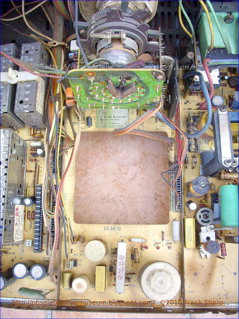


VIDOM DIAGNOSE SYSTEM OVERVIEW:


The ITT CHASSIS PIL ST. M. KABT. UFB9 58616606 is a semi modular chassis. The
VIDOM Diagnosesystem which stays for Voll Integriete Diagnose Optische Messpunkte wich is a Completely Optical Integrated measurements Diagnose Sytstem introduces new technolgy approach in fault diagnosing.
The system has the target to help the specialized and trained technician to evaluate faults in logical way.
The diagnosing system is based on led lamps which are informing realtively to the functional status of some main points, even derived, around the chassis, giving further information during diagnosing faults.
ITT IDEAL COLOR 1960 ST OSCAR 8 VIDOM CHASSIS PIL ST. M. KABT. UFB9 58616606 CIRCUIT ARRANGEMENT IN A PICTURE DISPLAY DEVICE UTILIZING A STABILIZED SUPPLY VOLTAGE CIRCUIT: (TDA3060)
Line synchronized switch mode power supply:
A
stabilized supply voltage circuit for a picture display device
comprising a chopper wherein the switching signal has the line frequency
and is duration-modulated. The coil of the chopper constitutes the
primary winding of a transformer a secondary winding of which drives the
line output transistor so that the switching transistor of the
chopper also functions as a driver for the line output stage. The
oscillator generating the switching signal may be the line oscillator.
In a special embodiment the driver and line output transistor conduct
simultaneously and in order to limit the base current of the line
output transistor a coil shunted by a diode is incorporated in the
drive line of the line output transistor. Other secondary windings of
the transformer drive diodes which conduct simultaneously with the
efficiency diode of the chopper so as to generate further stabilized
supply voltages.
 The
invention relates to a circuit arrangement in a picture display
device wherein the input direct voltage between two input terminals,
which is obtained be rectifying the mains alternating voltage, is
converted into a stabilized output direct voltage by means of a
switching transistor and a coil and wherein the transistor is connected
to a first input terminal and an efficiency diode is connected to the
junction of the transistor and the coil. The switching transistor is
driven by a pulsatory voltage of line frequency which pulses are
duration-modulated in order to saturate the switching transistor during
part of the period dependent on the direct voltage to be stabilized
and to cut off this transistor during the remaining part of the
period. The pulse duration modulation is effected by means of a
comparison circuit which compares the direct voltage to be stabilized
with a substantially constant voltage, the coil constituting the
primary winding of a transformer.
The
invention relates to a circuit arrangement in a picture display
device wherein the input direct voltage between two input terminals,
which is obtained be rectifying the mains alternating voltage, is
converted into a stabilized output direct voltage by means of a
switching transistor and a coil and wherein the transistor is connected
to a first input terminal and an efficiency diode is connected to the
junction of the transistor and the coil. The switching transistor is
driven by a pulsatory voltage of line frequency which pulses are
duration-modulated in order to saturate the switching transistor during
part of the period dependent on the direct voltage to be stabilized
and to cut off this transistor during the remaining part of the
period. The pulse duration modulation is effected by means of a
comparison circuit which compares the direct voltage to be stabilized
with a substantially constant voltage, the coil constituting the
primary winding of a transformer.Such a circuit arrangement is known from German "Auslegeschrift" 1.293.304. wherein a circuit arrangement is described which has for its object to convert an input direct voltage which is generated between two terminals into a different direct voltage. The circuit employs a switch connected to the first terminal of the input voltage and periodically opens and closes so that the input voltage is converted into a pulsatory voltage. This pulsatory voltage is then applied to a coil. A diode is arranged between the junction of the switch and the coil and the second terminal of the input voltage whilst a load and a charge capacitor in parallel thereto are arranged between the other end of the coil and the second terminal of the input voltage. The assembly operates in accordance with the known efficiency principle i.e., the current supplied to the load flows alternately through the switch and through the diode. The function of the switch is performed by a switching transistor which is driven by a periodical pulsatory voltage which saturates this transistor for a given part of the period. Such a configuration is known under different names in the literature; it will be referred to herein as a "chopper." A known advantage thereof, is that the switching transistor must be able to stand a high voltage or provide a great current but it need not dissipate a great power. The output voltage of the chopper is compared with a constant reference voltage. If the output voltage attempts to vary because the input voltage and/or the load varies, a voltage causing a duration modulation of the pulses is produced at the output of the comparison arrangement. As a result the quantity of the energy stored in the coil varies and the output voltage is maintained constant. In the German "Auslegeschrift" referred to it is therefore an object to provide a stabilized supply voltage device.
In
the circuit arrangement according to the mentioned German
"Auslegeschrift" the frequency of the load variations or a harmonic
thereof is chosen as the frequency for the switching voltage.
Particularly when the load fed by the chopper is the line deflection
circuit of a picture display device, wherein thus the impedance of the
load varies in the rhythm of the line frequency, the frequency of the
switching voltage is equal to or is a multiple of the line frequency.It
is to be noted that the chopper need not necessarily be formed as
that in the mentioned German "Auslegeschrift." In fact, it is known
from literature that the efficiency diode and the coil may be
exchanged. It is alternatively possible for the coil to be provided at
the first terminal of the input voltage whilst the switching
transistor is arranged between the other end and the second terminal
of the input voltage. The efficiency diode is then provided between
the junction of said end and the switching transistor and the load. It
may be recognized that for all these modifications a voltage is
present across the connections of the coil which voltage has the same
frequency and the same shape as the pulsatory switching voltage. The
control voltage of a line deflection circuit is a pulsatory voltage
which causes the line output transistor to be saturates and cut off
alternately. The invention is based on the recognition that the
voltage present across the connections of the coil is suitable to
function as such a control voltage and that the coil constitutes the
primary of a transformer. To this end the circuit arrangement
according to the invention is characterized in that a secondary
winding of the transformer drives the switching element which applies a
line deflection current to line deflection coils and by which the
voltage for the final anode of a picture display tube which forms part
of the picture display device is generated, and that the ratio
between the period during which the switching transistor is saturated
and the entire period, i.e., the switching transistor duty cycle is
between 0.3 and 0.7 during normal operation.The invention is also based on the recognition that the duration modulation which is necessary to stabilize the supply voltage with the switching transistor does not exert influence on the driving of the line output transistor. This resides in the fact that in case of a longer or shorter cut-off period of the line output transistor the current flowing through the line deflection coils thereof is not influenced because of the efficiency diode current and transistor current are taken over or, in case of a special kind of transistor, the collector-emitter current is taken over by the base collector current and conversely. However, in that case the above-mentioned ratios of 0.3 : 0.7 should be taken into account since otherwise this take-over principle is jeopardized.
 As
will be further explained the use of the switching transistor as a
driver for the line output transistor in an embodiment to be especially
described hereinafter has the further advantage that the line output
transistor automatically becomes non-conductive when this switching
transistor is short circuited so that the deflection and the EHT for
the display tube drop out and thus avoid damage thereof.
As
will be further explained the use of the switching transistor as a
driver for the line output transistor in an embodiment to be especially
described hereinafter has the further advantage that the line output
transistor automatically becomes non-conductive when this switching
transistor is short circuited so that the deflection and the EHT for
the display tube drop out and thus avoid damage thereof.Due to the step according to the invention the switching transistor in the stabilized supply functions as a driver for the line deflection circuit. The circuit arrangement according to the invention may in addition be equipped with a very efficient safety circuit so that the reliability is considerably enhanced, which is described in the U.S. Pat. No. 3,629,686. The invention is furthermore based on the recognition of the fact that the pulsatory voltage present across the connections of the coil is furthermore used and to this end the circuit arrangement according to the invention is characterized in that secondary windings of the transformer drive diodes which conduct simultaneously with the efficiency diode so as to generate further stabilized direct voltages, one end of said diodes being connected to ground.
In order that the invention may be readily carried into effect, a few embodiments thereof will now be described in detail by way of example with reference to the accompanying diagrammatic drawings in which:
FIG. 1 shows a principle circuit diagram wherein the chopper and the line deflection circuit are further shown but other circuits are not further shown.
FIGS. 2a, 2b and 2c show the variation as a function of time of two currents and of a voltage occurring in the circuit arrangement according to FIG. 1.
FIGS. 3a 3b, 3c and 3d show other embodiments of the chopper.
FIGS. 4a and 4b show modifications of part of the circuit arrangement of FIG. 1.
 In
FIG. 1 the reference numeral 1 denotes a rectifier circuit which
converts the mains voltage supplied thereto into a non-stabilized direct
voltage. The collector of a switching transistor 2 is connected to
one of the two terminals between which this direct voltage is
obtained, said transistor being of the npn-type in this embodiment and
the base of which receives a pulsatory voltage which originates
through a control stage 4 from a modulator 5 and causes transistor 2
to be saturated and cut off alternately. The voltage waveform 3 is
produced at the emitter of transistor 2. In order to maintain the
output voltage of the circuit arrangement constant, the duration of
the pulses provided is varied in modulator 5. A pulse oscillator 6
supplies the pulsatory voltage to modulator 5 and is synchronized by a
signal of line frequency which originates from the line oscillator 6'
present in the picture display device. This line oscillator 6' is in
turn directly synchronized in known manner by pulses 7' of line
frequency which are present in the device and originate for example
from a received television signal if the picture display device is a
television receiver. Pulse oscillator 6 thus generates a pulsatory
voltage the repetition frequency of which is the line frequency.The
emitter of switching transistor 2 is connected at one end to the
cathode of an efficiency diode 7 whose other end is connected to the
second input voltage terminal and at the other end to primary winding 8
of a transformer 9. Pulsatory voltage 3 which is produced at the
cathode of efficiency diode 7 is clamped against the potential of said
second terminal during the intervals when this diode conducts. During
the other intervals the pulsatory voltage 3 assumes the value V i .
A charge capacitor 10 and a load 11 are arranged between the other
end of winding 8 and the second input voltage terminal. The elements
2,7,8,10 and 11 constitute a so-called chopper producing a direct
voltage across charge capacitor 10, provided that capacitor 10 has a
sufficiently great value for the line frequency and the current applied
to load 11 flowing alternately through switching transistor 2 or
through efficiency diode 7. The output voltage V o which is
the direct voltage produced across charge capacitor 10 is applied to a
comparison circuit 12 which compares the voltage V o with
a reference voltage. Comparison circuit 12 generates a direct voltage
which is applied to modulator 5 so that the duration of the effective
period δ T of switching transistor 2 relative to the period T of
pulses 3 varies as a function of the variations of output voltage V 0 . In fact, it is readily evident that output voltage V o is proportional to the ratio δ :
In
FIG. 1 the reference numeral 1 denotes a rectifier circuit which
converts the mains voltage supplied thereto into a non-stabilized direct
voltage. The collector of a switching transistor 2 is connected to
one of the two terminals between which this direct voltage is
obtained, said transistor being of the npn-type in this embodiment and
the base of which receives a pulsatory voltage which originates
through a control stage 4 from a modulator 5 and causes transistor 2
to be saturated and cut off alternately. The voltage waveform 3 is
produced at the emitter of transistor 2. In order to maintain the
output voltage of the circuit arrangement constant, the duration of
the pulses provided is varied in modulator 5. A pulse oscillator 6
supplies the pulsatory voltage to modulator 5 and is synchronized by a
signal of line frequency which originates from the line oscillator 6'
present in the picture display device. This line oscillator 6' is in
turn directly synchronized in known manner by pulses 7' of line
frequency which are present in the device and originate for example
from a received television signal if the picture display device is a
television receiver. Pulse oscillator 6 thus generates a pulsatory
voltage the repetition frequency of which is the line frequency.The
emitter of switching transistor 2 is connected at one end to the
cathode of an efficiency diode 7 whose other end is connected to the
second input voltage terminal and at the other end to primary winding 8
of a transformer 9. Pulsatory voltage 3 which is produced at the
cathode of efficiency diode 7 is clamped against the potential of said
second terminal during the intervals when this diode conducts. During
the other intervals the pulsatory voltage 3 assumes the value V i .
A charge capacitor 10 and a load 11 are arranged between the other
end of winding 8 and the second input voltage terminal. The elements
2,7,8,10 and 11 constitute a so-called chopper producing a direct
voltage across charge capacitor 10, provided that capacitor 10 has a
sufficiently great value for the line frequency and the current applied
to load 11 flowing alternately through switching transistor 2 or
through efficiency diode 7. The output voltage V o which is
the direct voltage produced across charge capacitor 10 is applied to a
comparison circuit 12 which compares the voltage V o with
a reference voltage. Comparison circuit 12 generates a direct voltage
which is applied to modulator 5 so that the duration of the effective
period δ T of switching transistor 2 relative to the period T of
pulses 3 varies as a function of the variations of output voltage V 0 . In fact, it is readily evident that output voltage V o is proportional to the ratio δ :V o = V i . δ
However,
variations in the line amplitude and the EHT may occur as a result of
an insufficiently small internal impedance of the EHT generator.
Compensation means are known for this purpose. A possibility within the
scope of the present invention is to use comparison circuit 12 for
this purpose. In fact, if the beam current passes through an element
having a substantially quadratic characteristic, for example, a
voltage-dependent resistor, then a variation for voltage V o
may be obtained through comparison circuit 12 which variation is
proportional to the root of the variation in the EHT which is a known
condition for the line amplitude to remain constant.In addition this facilitates smoothing of voltage V o since the repetition frequency of pulsatory voltage 3 is many times higher than that of the mains and a comparatively small value may be sufficient for charge capacitor 10. If charge capacitor 10 has a sufficiently high value for the line frequency, voltage V o is indeed a direct voltage so that a voltage having the same form as pulsatory voltage 3 is produced across the terminals of primary winding 8. Thus voltages which have the same shape as pulsatory voltage 3 but have a greater or smaller amplitude are produced across secondary windings 13, 14 of transformer 9 (FIG. 1 shows only 2 secondary windings but there may be more). The invention is based on the recognition that one end of each secondary winding is connected to earth while the other end thereof drives a diode, the winding sense of each winding and the direction of conductance of each diode being chosen to be such that these diodes conduct during the same period as does efficiency diode 7. After smoothing, stabilized supply voltages, for example, at terminal 15 are generated in this manner at the amplitudes and polarities required for the circuit arrangements present in the picture display device. In FIG. 1 the voltage generated at terminal 15 is, for example, positive relative to earth. It is to be noted that the load currents of the supply voltages obtained in this manner cause a reduction of the switching power which is economized by efficiency diode 7. The sum of all diode currents including that of diode 7 is in fact equal to the current which would flow through diode 7 if no secondary winding were wound on transformer 9 and if no simultaneous diode were used. This reduction may be considered an additional advantage of the circuit arrangement according to the invention, for a diode suitable for smaller powers may then be used. However, it will be evident that the overall secondary load must not exceed the primary load since otherwise there is the risk of efficiency diode 7 being blocked so that stabilization of the secondary supply voltages would be out of the question.
It is to be noted that a parabola voltage of line frequency as shown at 28 is produced across the charge capacitor 10 if this capacitor is given a smaller capacitance so that consequently the so-called S-correction is established.
In FIG. 1 charge capacitors are arranged between terminals 15 etc. and earth so as to ensure that the voltages on these points are stabilized direct voltages. If in addition the mean value of the voltage on one of these terminals has been made equal to the effective value of the alternating voltage which is required for heating the filament of the picture display tube present in the picture display device, this voltage is suitable for this heating. This is a further advantage of the invention since the cheap generation of a stabilized filament voltage for the picture display tube has always been a difficult problem in transistorized arrangements.
A
further advantage of the picture display device according to the
invention is that transformer 9 can function as a separation
transformer so that the different secondary windings can be separated
from the mains and their lower ends can be connected to ground of the
picture display device. The latter step makes it possible to connect a
different apparatus such as, for example, a magnetic recording and/or
playback apparatus to the picture display device without earth
connection problems occurring.In FIG. 1 the reference numeral 14 denotes a secondary winding of transformer 9 which in accordance with the previously mentioned recognition of the invention can drive line output transistor 16 of the line deflection circuit 17. Line deflection circuit 17 which is shown in a simplified form in FIG. 1 includes inter alia line deflection coils 18 and an EHT transformer 19 a secondary winding 20 of which serves for generating the EHT required for the acceleration anode of the picture display tube. Line deflection circuit 17 is fed by the output voltage V o of the chopper which voltage is stabilized due to the pulse duration modulation with all previously mentioned advantages. Line deflection circuit 17 corresponds, for example, to similar arrangements which have been described in U.S. Pat. No. 3,504,224 issued Mar. 31, 1970 to J.J. Reichgelt et al., U.S. patent application Ser. No. 737,009 filed June 14, 1968 by W. H. Hetterscheid and U.S. application Ser. No. 26,497 filed April 8, 1970 by W. Hetterscheid et al. It will be evident that differently formed lined deflection circuits are alternatively possible.
It
will now be shown that secondary winding 14 can indeed drive a line
deflection circuit so that switching transistor 2 can function as a
driver for the line deflection. FIGS. 2a and b show the variation as a
function of time of the current i C which flows in the collector of transistor 16 and of the drive voltage v 14 across the terminals of secondary winding 14. During the flyback period (0, t 1 ) transistor 16 must be fully cut off because a high voltage peak is then produced at its collector; voltage v 14 must then be absolutely negative. During the scan period (t 1 , t 4 ) a sawtooth current i C
flows through the collector electrode of transistor 16 which current
is first negative and then changes its direction. As the circuit
arrangement is not free from loss, the instant t 3 when current i C becomes zero lies, as is known, before the middle of the scan period. At the end t 4
of the scan period transistor 16 must be switched off again. However,
since transistor 16 is saturated during the scan period and since
this transistor must be suitable for high voltages and great powers so
that its collector layer is thick, this transistor has a very great
excess of charge carriers in both its base and collector layers. The
removal of these charge carriers takes a period t s which
is not negligible whereafter the transistor is indeed switched off.
Thus the fraction δ T of the line period T at which v 14 is positive must end at the latest at the instant (t 4 - t s ) located after the commencement (t = 0) of the previous flyback.The time δ T may be initiated at any instant t 2 which is located between the end t 1 of the flyback period and the instant t 3 when collector current i C reverses its direction. It is true that emitter current flows through transistor 16 at the instant t 2 , but collector current i C is not influenced thereby, at least not when the supply voltage (= V o )
for line deflection circuit 17 is high enough. All this has been
described in the U.S. Pat. No. 3,504,224. The same applies to line
deflection circuits wherein the collector base diode does not function
as an efficiency diode as is the case in the described circuit 17, but
wherein an efficiency diode is arranged between collector and emitter
of the line output transistor. In such a case the negative part of the
current i C of FIG. 2a represents the current flowing through the said efficiency diode.After the instant t 3 voltage v 14 must be positive. In other words, the minimum duration of the period T when voltage v 14 must be positive is (t 4 - t s ) - t 3 whilst the maximum duration thereof is (t 4 - t s ) - t 1 . In a television system employing 625 lines per raster the line period t 4 is approximately 64 μus and the flyback period is approximately 12 μus. Without losses in the circuit arrangement instant t 3 would be located approximately 26 μus after the instant t 1 , and with losses a reasonable value is 22 μus which is 34 μus after the commencement of the period. If for safety's sake it is assumed that t s lasts approximately 10 μus, the extreme values of δ T are approximately 20 and 42 μus and consequently the values for δ are approximately 0.31 and 0.66 at a mean value which is equal to approximately 0.49. It was previously stated that a mean value of δ = 0.5 was suitable. Line deflection circuit 17 can therefore indeed be used in combination with the chopper in the manner described, and the relative variation of δ may be (0.66 - 0.31) : 0.49 = 71.5 percent. This is more than necessary to obviate the variations in the mains voltage or in the various loads and to establish the East-West modulation and ripple compensation to be described hereinafter. In fact, if it is assumed that the mains voltage varies between -15 and +10 percent of the nominal value of 220 V, while the 50 Hz ripple voltage which is superimposed on the input voltage V i has a peak-to-peak value of 40 V and V i is nominally 270 V, then the lowest occurring V i is:
0.85 × 270 V - 20 V = 210 V and the highest occurring V i is
1.1 × 270 V + 20 V = 320 V. For an output voltage V o of 135 V the ratio must thus vary between
δ = 135 : 210 = 0.64 and δ = 135 : 320 = 0.42.
A
considerable problem presenting itself is that of the simultaneous or
non-simultaneous drive of line output transistor 16 with switching
transistor 2, it being understood that in case of simultaneous drive
both transistors are simultaneously bottomed, that is during the period δ
T. This depends on the winding sense of secondary winding 14 relative
to that of primary winding 8. In FIG. 1 it has been assumed that the
drive takes place simultaneously so that the voltage present across
winding 14 has the shape shown in FIG. 2b. This voltage assumes the
value n(V i - V o ) in the period δ T and the
value -nVo in the period (1 - δ )T, wherein n is the ratio of the number
of turns on windings 14 and 8 and wherein V o is maintained constant at nominal mains voltage V o = δ V inom . However, if as a result of an increase or a decrease of the mains voltage V i increases or decreases proportionally therewith, i.e., V i = V i nom + Δ V, the positive portion of V 14 becomes equal to n(V i nom - V o +Δ V) = n [(1 -δ)V i nom +ΔV] = n(0.5 V inom +ΔV) if δ = 0.5 for V i = V i nom. Relatively, this is a variation which is twice as great. For example, if V i nom = 270 V and V o = 135 V, a variation in the mains voltage of from -15 to +10 percent causes a variation of V i
of from -40.5 V to +27 V which ranges from -30 to +20 percent of 135 V
which is present across winding 8 during the period δ T. The result
is that transistor 16 can always be bottomed over a large range of
variation. If the signal of FIG. 2b would be applied through a resistor
to the base of transistor 16, the base current thereof would have to
undergo the same variation while the transistor would already be
saturated in case of too low a voltage. In this case it is assumed that
transformer 9 is ideal (without loss) and that coil 21 has a small
inductance as is explained in the U.S. patent application Ser. No.
737,009 above mentioned. It is therefore found to be desirable to limit
the base current of transistor 16.This
may be effected by providing a coil 22 having a large value
inductance, approximately 100 μH, between winding 14 and the small coil
21. The variation of said base current i b is shown in
FIG. 2c but not to the same scale as the collector current of FIG. 2a.
During the conducting interval δ T current i b varies as a
linear function of time having a final value of wherein L represents
the inductance of coil 22. This not only provides the advantage that
this final value is not immediately reached, but it can be shown that
variation of this final value as a function of the mains voltage has
been reduced, for there applies at nominal mains voltage that: If the
mains voltage V i = V i nom +Δ V, then ##SPC1## because V i nom = 2 V o . Thus this variation is equal to that of the mains voltage and is not twice as great. During switching off, t 2 ,
of transistor 16 coil 22 must exert no influence and coil 21 must
exert influence which is achieved by arranging a diode 23 parallel to
coil 22. Furthermore the control circuit of transistor 16 in this
example comprises the two diodes 24 and 25 as described in U.S.
application Ser. No. 26,497 above referred to, wherein one of these
diodes, diode 25 in FIG. 1, must be shunted by a resistor.
During switching off, t 2 ,
of transistor 16 coil 22 must exert no influence and coil 21 must
exert influence which is achieved by arranging a diode 23 parallel to
coil 22. Furthermore the control circuit of transistor 16 in this
example comprises the two diodes 24 and 25 as described in U.S.
application Ser. No. 26,497 above referred to, wherein one of these
diodes, diode 25 in FIG. 1, must be shunted by a resistor.The control circuit of transistor 16 may alternatively be formed as is shown in FIG. 4. In fact, it is known that coil 21 may be replaced by the parallel arrangement of a diode 21' and a resistor 21" by which the inverse current can be limited. To separate the path of the inverse current from that of the forward current the parallel arrangement of a the diode 29' and a resistor 29" must then be present. This leads to the circuit arrangement shown in the upper part of FIG. 4. This circuit arrangement may now be simplified if it is noted that diodes 25 and 21' on the one hand and diodes 23 and 29' on the other hand are series-arranged. The result is shown in the lower part of FIG. 4 which, as compared with the circuit arrangement of FIG. 1, employs one coil less and an additional resistor.
FIG. 3 shows possible modifications of the chopper. FIG. 3a shown in a simplified form the circuit arrangement according to FIG. 1 wherein the pulsatory voltage present across the connections of windings 8 has a peak-to-peak amplitude of V i - V o = 0.5 V i for δ = 0.5, As has been stated, the provision of coil 22 gives a relative variation for the base current of transistor 16 which is equal to that of the mains voltage. In the cases according to FIG. 3b, 3c and 3d the peak-to-peak amplitude of the voltage across winding 8 is equal to V i so that the provision of coil 22 results in a relative variation which is equal to half that of the mains voltage which is still more favorable than in the first case.
Transistors
of the npn type are used in FIG. 3. If transistors of the pnp type
are used, the relevant efficiency diodes must of course be reversed.In this connection it is to be noted that it is possible to obtain an output voltage V o with the aid of the modifications according to FIGS. 3b, c and d, which voltage is higher than input voltage V i . These modifications may be used in countries such as, for example, the United of America or France where the nominal mains voltage is 117 or 110 V without having to modify the rest of the circuit arrangement.
The above-mentioned remark regarding the sum of the diode currents only applies, however, for the modifications shown in FIGS. 3a and d.
If line output transistor 16 is not simultaneously driven with switching transistor 2, efficiency diodes 7 conducts simultaneously with transistor 16 i.e., during the period which is denoted by δ T in FIGS. 1 and 2b. During that period the output voltage V o of the chopper is stabilized so that the base current of transistor 16 is stabilized without further difficulty. However, a considerable drawback occurs. In FIG. 1 the reference numeral 26 denotes a safety circuit the purpose of which is to safeguard switching transistor 2 when the current supplied to load 11 and/or line deflection circuit 17 becomes to high, which happens because the chopper stops. After a given period output voltage V o is built up again, but gradually which means that the ratio δ is initially small in the order of 0.1. All this is described in U.S. patent No. 3,629,686. The same phenomenon occurs when the display device is switched on. Since δ = 0.1 corresponds to approximately 6 μs when T = 64 μs, efficiency diode 7 conducts in that case for 64 - 6 = 58 μus so that transistor 16 is already switched on at the end of the scan or at a slightly greater ratio δ during the flyback. This would cause an inadmissibly high dissipation. For this reason the simultaneous drive is therefore to be preferred.
 Pulse
oscillator 6 applies pulses of line frequency to modulator 5. It may
be advantageous to have two line frequency generators as already
described, to wit pulse oscillator 6 and line oscillator 6' which is
present in the picture display device and which is directly synchronized
in known manner by line synchronizing pulses 7'. In fact, in this
case line oscillator 6' applies a signal of great amplitude and free
from interference to pulse oscillator 6. However, it is alternatively
possible to combine pulse oscillator 6 and line oscillator 6' in one
single oscillator 6" (see FIG. 1) which results in an economy of
components. It will be evident that line oscillator 6' and oscillator 6"
may alternatively be synchronized indirectly, for example, by means
of a phase discriminator. It is to be noted neither pulse oscillator
6, line oscillator 6' and oscillator 6" nor modulator 5 can be fed by
the supply described since output voltage V o is still not
present when the mains voltage is switched on. Said circuit
arrangements must therefore be fed directly from the input terminals.
If as described above these circuit arrangements are to be separated
from the mains, a small separation transformer can be used whose
primary winding is connected between the mains voltage terminals and
whose secondary winding is connected to ground at one end and controls
a rectifier at the other end.
Pulse
oscillator 6 applies pulses of line frequency to modulator 5. It may
be advantageous to have two line frequency generators as already
described, to wit pulse oscillator 6 and line oscillator 6' which is
present in the picture display device and which is directly synchronized
in known manner by line synchronizing pulses 7'. In fact, in this
case line oscillator 6' applies a signal of great amplitude and free
from interference to pulse oscillator 6. However, it is alternatively
possible to combine pulse oscillator 6 and line oscillator 6' in one
single oscillator 6" (see FIG. 1) which results in an economy of
components. It will be evident that line oscillator 6' and oscillator 6"
may alternatively be synchronized indirectly, for example, by means
of a phase discriminator. It is to be noted neither pulse oscillator
6, line oscillator 6' and oscillator 6" nor modulator 5 can be fed by
the supply described since output voltage V o is still not
present when the mains voltage is switched on. Said circuit
arrangements must therefore be fed directly from the input terminals.
If as described above these circuit arrangements are to be separated
from the mains, a small separation transformer can be used whose
primary winding is connected between the mains voltage terminals and
whose secondary winding is connected to ground at one end and controls
a rectifier at the other end.Capacitor 27 is arranged parallel to efficiency diode 7 so as to reduce the dissipation in switching transistor 2. In fact, if transistor 2 is switched off by the pulsatory control voltage, its collector current decreases and its collector-emitter voltage increases simultaneously so that the dissipated power is not negligible before the collector current has becomes zero. If efficiency diode 7 is shunted by capacitor 27 the increase of the collector-emitter voltage is delayed i.e., this voltage does not assume high values until the collector current has already been reduced. It is true that in that case the dissipation in transistor 2 slightly increases when it is switched on by the pulsatory control voltage but on the other hand since the current flowing through diode 7 has decreased due to the presence of the secondary windings, its inverse current is also reduced when transistor 2 is switched on and hence its dissipation has become smaller. In addition it is advantageous to delay these switching-on and switching-off periods to a slight extent because the switching pulses then contain fewer Fourier components of high frequency which may cause interferences in the picture display device and which may give rise to visible interferences on the screen of the display tube. These interferences occupy a fixed position on the displayed image because the switching frequency is the line frequency which is less disturbing to the viewer. In a practical circuit wherein the line frequency is 15,625 Hz and wherein switching transistor 2 is an experimental type suitable for a maximum of 350 V collector-emitter voltage or 1 A collector current and wherein efficiency diode 7 is of the Philips type BA 148 the capacitance of capacitor 27 is approximately 680 pF whilst the load is 70 W on the primary and 20 W on the secondary side of transformer 9. The collector dissipation upon switching off is 0.3 W (2.5 times smaller than without capacitor 27) and 0.7 W upon switching on.
As is known the so-called pincushion distortion is produced in the picture display tubes having a substantially flat screen and large deflection angles which are currently used. This distortion is especially a problem in color television wherein a raster correction cannot be brought about by magnetic means. The correction of the so-called East-West pincushion distortion i.e., in the horizontal direction on the screen of the picture display tube can be established in an elegant manner with the aid of the circuit arrangement according to the invention. In fact, if the voltage generated by comparison circuit 12 and being applied to modulator 5 for duration-modulating pulsatory voltage 3 is modulated by a parabola voltage 28 of field frequency, pulsatory voltage 3 is also modulated thereby. If the power consumption of the line deflection circuit forms part of the load on the output voltage of the chopper, the signal applied to the line deflection coils is likewise modulated in the same manner. Conditions therefore are that the parabola voltage 28 of field frequency has a polarity such that the envelope of the sawtooth current of line frequency flowing through the line deflection coils has a maximum in the middle of the scan of the field period and that charge capacitor 10 has not too small an impedance for the field frequency. On the other hand the other supply voltages which are generated by the circuit arrangement according to the invention and which might be hampered by this component of field frequency must be smoothed satisfactorily.
A practical embodiment of the described example with the reference numerals given provides an output for the supply of approximately 85 percent at a total load of 90 W, the internal resistance for direct current loads being 1.5 ohms and for pulsatory currents being approximately 10 ohms. In case of a variation of ± 10 percent of the mains voltage, output voltage V o is stable within 0.4 V. Under the nominal circumstances the collector dissipation of switching transistor 2 is approximately 2.5 W.
Since the internal resistance of the supply is so small, it can
be
used advantageously, for example, at terminal 15 for supplying a
class-B audio amplifier which forms part of the display device. Such
an amplifier has the known advantages that its dissipation is directly
proportional to the amplitude of the sound to be reproduced and that
its output is higher than that of a class-A amplifier. On the other
hand a class-A amplifier consumes a substantially constant power so
that the internal resistance of the supply voltage source is of little
importance. However, if this source is highly resistive, the supply
voltage is modulated in the case of a class-B amplifier by the audio
information when the sound intensity is great which may detrimentally
influence other parts of the display device. This drawback is prevented
by means of the supply according to the invention.The 50 Hz ripple voltage which is superimposed on the rectified input voltage V i is compensated by comparison circuit 12 and modulator 5 since this ripple voltage may be considered to be a variation of input voltage V i . A further compensation is obtained by applying a portion of this ripple voltage with suitable polarity to comparison circuit 12. It is then sufficient to have a lower value for the smoothing capacitor which forms part of rectifier circuit 1 (see FIG. 3). The parabola voltage 28 of field frequency originating from the field time base is applied to the same circuit 12 so as to correct the East-West pincushion distortion.
ULTRASONIC REMOTE CONTROL RECEIVER ITT IDEAL COLOR 1960 ST OSCAR 8 VIDOM CHASSIS PIL ST. M. KABT. UFB9 58616606
An ultrasonic remote control receiver wherein an incoming ultrasonic signal is converted to square wave pulses of the same frequency by a Schmitt trigger circuit; digital circuits are thereafter used to count pulses resulting from the incoming signal over a predetermined period of time; a decoder activates one of a plurality of outputs in dependance to the number of pulses counted, provision is made to prevent interference signals from producing undesired control outputs.

1. An ultrasonic remote control receiver for applying a control signal to a selected one of a plurality of control channels in response to and dependent on the frequency of a received ultrasonic signal comprising:
2. An ultrasonic remote control receiver comprising:
3. An ultrasonic remote control receiver comprising:
4. The ultrasonic remote control receiver as defined in claim 3, wherein said means producing square pulses is a Schmitt trigger circuit and said means providing a signal input to said sequence controller is a retriggerable monostable multivibrator.
5. An ultrasonic remote control receiver comprising:
6. An ultrasonic remote control receiver comprising:
7. An ultrasonic remote control receiver as defined in claim 6 further comprising a monostable multivibrator between the output of said Schmitt trigger circuit and the remaining elements of said receiver.
8. An ultrasonic remote control receiver as defined in claim 6 further comprising a bistable multivibrator between the output of said Schmitt trigger circuit and the remaing elements of said receiver.
9. The ultrasonic remote control receiver as defined in claim 7 wherein the hold period of said monostable multivibrator is slightly less than one half the period of said square wave pulses from said Schmitt trigger circuit.
To obtain the simplest possible transmitter construction in ultrasonic remote control, modulation of the emitted ultrasonic frequencies is not employed; to control different operations different frequencies are emitted which must be recognized in the receiver and evaluated for carrying out the different functions associated therewith. Presently, to recognize the different frequencies, use is made of resonant circuits, each of which contains one or more coils tuned in each case together with a capacitor to one of the useful frequencies.
These hitherto known receivers have numerous disadvantages. Thus, for example, before starting operation of the receiver a time-consuming alignment procedure must be carried out with which the resonant frequencies of the individual resonant circuits are set. Since it is inevitable that with time the resonant circuits become detuned, it may be necessary to repeat the alignment procedure.
A further disadvantage is that the known receivers cannot be made by integrated techniques because the coils used therein are not suitable for such techniques.
The problem underlying the invention is thus to provide an ultrasonic remote control receiver of the type mentioned at above which is extremely simple to set and in addition can be made by integrated techniques.
To solve this problem, according to the invention an ultrasonic remote control receiver of the type mentioned above contains a counter for counting the useful frequency oscillations received during a fixed measuring time, a sequence control device which determines the measuring time and which is started on receipt of a useful frequency, and a decoder comprising several outputs which is connected to the outputs of the counter, said decoder emitting a control signal at the output associated with the count reached at the end of the measuring time.
In the receiver constructed according to the invention the frequency emitted by the transmitter is identified by counting the oscillations received during a measuring time. The evaluation of the count reached at the end of the measuring time takes place in a decoder which emits a control signal at a certain output according to the count. The measuring time is fixed by a sequence control device which is set in operation on receipt of useful frequency signals.
In such a receiver the only quantity which has to be exactly fixed is the measuring time; it is therefore no longer necessary to align components to certain frequencies. Since no coils are required, the novel receiver can also be made up of integrated circuits.
A further development of the invention resides in that an interference identifying device is provided which on receipt of interference frequencies differing from the useful frequencies interrupts the operation of the sequence control device.
Hitherto known ultrasonic remote control receivers respond to any oscillation received if the frequency thereof has a value which excites a resonant circuit in the receiver. There is no way of distinguishing between oscillations received from the remote control transmitter and from interference sources.
Interfering ultrasonic oscillations may be due to many different causes. For example, noises such as hand clapping, rattling of short keys such as safety keys, operating cigarette lighters, rattling of crockery and the like cover a frequency spectrum reaching from the audio frequency range far into the ultrasonic region. The ultrasonic components may have the effect of simulating a useful frequency and cause an erroneous function in the receiver.
The interference identifying device according to the further development is constructed in such a manner that it recognizes oscillations having frequencies deviating from the useful frequencies and as a result of this recognition switches off the sequence control device. This switching off prevents the counter state reached from being passed to the decoder and consequently the latter cannot emit an erroneous control signal.
With this further development of the ultrasonic remote control receiver the operation of equipment such as radio and television sets is made extremely reliable and interference-free. During the operation of such a set it is no longer possible for the remote control to become operative, triggered by interference noises, eliminating for example the possibility of unintentional program or volume changes.
Examples of embodiment of the invention are illustrated in the drawings, wherein:
FIG. 1 shows a block circuit diagram of a remote control receiver according to the invention;
FIG. 2 is a diagram explaining the mode of operation of the circuit according to FIG. 1;
FIG. 3 shows another embodiment of the invention;
FIG. 4 is a diagram explaining the mode of operation of the circuit according to FIG. 3;
FIG. 5 is a diagram illustrating interference frequency identification in the circuit according to FIG. 3;
FIG. 6 shows a block circuit diagram of another embodiment of part of the circuit according to FIG. 3;
FIG. 7 is a diagram explaining the mode of operation of the embodiment according to FIG. 6;
FIG. 8 is a block circuit diagram of a further embodiment of a part of the circuit according to FIG. and, an
FIG. 9 is a diagram explaining the mode of operation of the embodiment according to FIG. 8.
 The
ultrasonic remote control receiver shown in FIG. 1 comprises an
input 1 which is connected to an ultrasonic microphone intended to
receive ultrasonic signals coming from a remote control transmitter.
For each function to be performed by the receiver the remote control
transmitter emits one of several unmodulated different useful
frequencies which are spaced from each other a constant channel
spacing Δ f and which all lie within a useful frequency band.
The
ultrasonic remote control receiver shown in FIG. 1 comprises an
input 1 which is connected to an ultrasonic microphone intended to
receive ultrasonic signals coming from a remote control transmitter.
For each function to be performed by the receiver the remote control
transmitter emits one of several unmodulated different useful
frequencies which are spaced from each other a constant channel
spacing Δ f and which all lie within a useful frequency band.To obtain a signal which is as free as possible from noise at the input 1, a band filter and a limiting amplifier are preferably incorporated between the ultrasonic microphone and the input 1. The band filter may be made up of two active filters whose resonant frequencies are offset with respect to each other so that a pass band curve in the useful frequency band is obtained which is as flat as possible.
The input 1 leads to a Schmitt trigger 2 which converts the electrical signal applied thereto with the frequency of the ultrasonic signal to a sequence of rectangular pulses. The output 3 of the Schmitt trigger 2 is connected to the input 6 of a frequency divider 7 which is in operation for the duration of a control pulse applied to its control input 8 and divides the recurrence frequency of the pulses supplied thereto at the input 6 thereof in a constant division ratio. The output 9 of the frequency divider 7 is connected to the input 10 of a counter 11 which counts the pulses coming from the frequency divider 7. The counter 11 is a four-stage binary counter whose stage outputs are connected to the inputs of a store (register) 12 which is so constructed that on application of a control pulse to the input 12 thereof it takes on the counter state in the counter 11 and stores said counter state until the next pulse at the input 13. The stage outputs of the store 12 are fed to the inputs of a decoder 14 which decodes the counter state contained in the store 12 in such a manner that a control signal is emitted at that one of its outputs D0 to D9 which is associated with the decoded counter state.
The output 3 of the Schmitt trigger 2 is also connected to the input 4 of a monoflop 5 which is brought into its operating state by each pulse at the output 3 of the Schmitt trigger. It returns from this operating state to its quiescent state after expiration of a hold time depending on its intrinsic time constant if it does not receive a new pulse prior to expiration of this hold time. It is held in the operating state by each pulse received during the hold time until it finally flops back into the quiescent state when the interval between two successive pulses is greater than its hold time.
The output 15 of the monoflop circuit 5 is connected to the input 16 of a sequence control device 17 which is set in operation by the signal emitted in the operating state of the monoflop 5. Supplied
to the sequence control device by 17 via a Schmitt trigger 18 at a control input 19 are pulses having a recurrence frequency derived from oscillations of the same frequency, for example, twice the mains frequency of 100 c/s, applied to the input 20. The sequence control device 17 is so constructed that in a cyclically recurring sequence in time with the pulses supplied to it at the input 19 it emits pulses at the outputs 21, 22 and 23 whose duration is equal to the period of the oscillation applied to the input 20. The output 21 of the sequence control device 17 is connected to the control input 8 of the frequency divider 7, the output 22 is connected to the control input 13 of the store 12 and the output 23 thereof is connected to the reset input 24 of the counter 11.
The mode of operation of the circuit of FIG. 1 will now be explained with the aid of the diagram of FIG. 2
 which
shows the variation with time of the signals at the output 3 of the
Schmitt trigger 2 and at the inputs 16 and 19 as well as the outputs
21, 22 and 23 of the sequence control device 17.
which
shows the variation with time of the signals at the output 3 of the
Schmitt trigger 2 and at the inputs 16 and 19 as well as the outputs
21, 22 and 23 of the sequence control device 17.It will be assumed that a useful frequency oscillation is being received at the input 1. The Schmitt trigger 2 then emits at the output 3 rectangular pulses whose recurrence frequency is equal to the frequency of said useful frequency oscillation. The first pulse emitted by the Schmitt trigger 2 puts the monoflop 5 into its operating state. The hold time of the monoflop 5 is so dimensioned that for all useful frequencies occurring it is longer than the recurrence period of the rectangular pulses emitted at the output 3. The monoflop 5 therefore remains in its operating state for as long as the useful frequency oscillation is applied to the input 1 and supplies to the control input 16 of the sequence control device 17 a control signal throughout this time.
Due to the control signal applied to the input 16 the sequence control device 17 emits at its outputs 21, 22 and 23 in time with the pulses supplied to it via the Schmitt trigger 18 at the input 19 mutually offset control pulse sequences, the duration of the control pulses being equal to the time interval of the leading edges of the pulses supplied at the input 19 and thus equal to the period of the oscillation applied to the input 20 and the pulse sequences being offset with respect to each other by one pulse duration. The control pulses emitted by the sequence control device 17 perform the following functions:
a. The first control pulse appearing at the output 21 sets in operation for its duration via the input 8 the frequency divider 7 so that the latter divides the recurrence frequency of the pulses supplied thereto from the Schmitt trigger 2 and thus the frequency of the useful frequency oscillations received in a constant ratio and passes counting pulses to the input 10 of the counter 11 with a correspondingly reduced recurrence frequency.
b. Via the input 13 the second pulse occurring at the output 22 causes the store 12 to take on and to store the count of the counter 11 reached at the end of the first control pulse.
c. The third control pulse appearing at the output 23 resets the counter 11 via the reset input 24.
COntrol pulse sequences continue to be emitted for as long as the monoflop 5 remains in its operating state.
Since the stage outputs of the store 12 are permanently connected to the inputs of the decoder 14, the store content is continuously being decoded. The decoder 14 therefore emits a control signal at the output which is associated with the count contained in the store.
During each group of three offset control pulses of the three control pulse sequences emitted by the sequence control device 17, the counter 11 receives counting pulses from the frequency divider 8 only for the duration of the control pulse of the first control pulse sequence emitted at the output 21. The duration of this control pulse thus determines the measuring time during which the oscillations of the useful frequency signal received are counted. Since the duration of the control pulses emitted by the sequence control device 17 is however equal to the period of the oscillation applied to the input 20, the measuring time is fixed by the period of said oscillation.
The frequency divider 7 is connected in front of the counter 11 so that a small capacity of the counter 11 is sufficient to obtain a clear indication of the received frequency even when the measuring time is so long that a large number of periods of the useful frequency oscillation is received during the measuring time. This is for example, the case when the oscillation supplied to the input 20 has twice the mains frequency. Since the frequency divider 7 divides the frequency of the useful frequency oscillations received in the constant ratio k, the counter 11 need count only the oscillations having a correspondingly reduced frequency. If the division ratio k of the divider 7 is so set that it is equal to the product of the measuring time t and channel spacing Δ f, only a frequency which differs by at least the channel spacing Δ f from a previously received frequency will change the count of the counter 11.
The purpose of the monoflop 5 is to prevent interference frequencies supplied to the input 1 from producing at one of the outputs D0 to D9 of the decoder 14 a control signal which could lead to an erroneous function of the equipment being controlled. The interference sources usually encountered emit a frequency spectrum whose components lie predominantly in the audio region, i.e., below the ultrasonic region. If the hold time of the monoflop 5 is set to a value slightly greater than the period of the smallest useful frequency but smaller than the period of the highest interference frequency occurring, the monoflop 5 returns to its quiescent state before the end of the period of an interference frequency. Since in this state no signal is supplied to the control input 16 of the sequence control device 17, the latter is put out of operation and consequently the received signal cannot be evaluated because the count of the counter 11 is not transferred to the store 12 and thus no decoding takes place.
To facilitate understanding of the invention, the function of the circuit of FIG. 1 will now be explained numerically by way of example. The channel spacing Δ f will be taken as 1,200 c/s so that for a frequency of 100 c/s of the oscillation applied to the input 20 and thus a measuring time of 10 ms a division ratio of the frequency divider 7 of k = t . Δf = 12 results. It will further be assumed that ten different channel frequencies are to be evaluated; the counter 11 is therefore so connected that it has a capacity of 10. With these values, during the measuring time the counter 11 runs through several count cycles. This means that for the received frequency during the measuring time the counter 11 reaches its maximum count several times and then starts counting again from the beginning. The count reached at the end of the measuring time is however still a clear indication of the received useful frequency provided the number of useful frequencies having a channel spacing Δf is at the most equal to the counter capacity Z. The relationship between the useful frequency f received and the count reached at the end of each measuring time t while this useful frequency is being received is expressed by the following equation:
f = (k/t) . (n . Z + m + 0.5)
wherein
f = useful frequency received in c/s
t = measuring time in seconds
k = division ratio of the frequency divider 7
Z = capacity of the counter 11
n = number of count cycles passed through (integral)
m = count
The term 0.5 in brackets is a correction factor which ensures that a new count is reached whenever the received frequency differs at least by half the channel spacing Δf from the channel center frequency of the neighboring channel. With a channel spacing Δ of 1,200 c/s, a measuring time t of 10 ms, a division ratio k of the frequency divider 7 of 12, a capacity Z of the counter 11 of 10 and an input frequency f of 33 k c/s, the count 7 is for example reached after two complete count cycles. This is because the input frequency of 33 k c/s is first divided by 12 by the frequency divider 7 so that pulses having a recurrence frequency of 2.750 k c/s reach the input 10 of the counter 11. Since the frequency divider 7 emits counting pulses only during the measuring time of 10 ms, during said time only 27.5 pulses reach the input 10 of the counter 11. For this number of pulses the counter thus runs through two complete cycles and finally stops at the count 7. Similarly, for an input frequency of 39 k c/s the counter stops at the count 2 after passing through three complete counter cycles. With the numerical values given up to 10 different frequencies may be received without any ambiguity occurring in the evaluation.
FIG. 3 illustrates a further embodiment of an ultrasonic remote control receiver which differs from the embodiment described above primarily in that to fix the measuring time it is not necessary to supply a reference frequency.
 In
the illustration of FIG. 3 the same reference numerals as in FIG. 1
are used for identical circuit components. The part of the circuit
enclosed in the dashed line represents the sequence control device 17'
which emits at its outputs 21', 22', 23' control signals which have
substantially the same functions as the control signals emitted at the
outputs 21, 22 and 23 of the sequence control device 17 of FIG. 1.
In
the illustration of FIG. 3 the same reference numerals as in FIG. 1
are used for identical circuit components. The part of the circuit
enclosed in the dashed line represents the sequence control device 17'
which emits at its outputs 21', 22', 23' control signals which have
substantially the same functions as the control signals emitted at the
outputs 21, 22 and 23 of the sequence control device 17 of FIG. 1.The useful frequency signal received is again supplied to the input 1. The input 1 is connected to the input of the Schmitt trigger 2 which again converts the input useful frequency oscillations into a sequence of pulses whose recurrence frequency is equal to the input useful frequency. The output 3 of the Schmitt trigger 2 is connected to the input B1 of a monoflop 25 which is contained in the sequence control device 17' and which is so constructed that it is switched to its operating state by a pulse received at the input B1 but during its hold time cannot be tripped again by any further pulse. The output 3 of the Schmitt trigger 2 is also connected to the input 26 of an AND gate 27 whose other input 28 is connected to that output 21' of the sequence control device 17' which is directly connected to the output Q1 of the monoflop 25. The output Q1 of the monoflop 25 which emits the signal complementary to the signal at the output Q1 is connected to the input B2 of a further monoflop 29 whose output Q2 is connected to the input A1 of the monoflop 25. The input 10 of the counter 11 is connected to the output of the AND gate 27. The stage outputs of the counter 11 are connected to the inputs of a gate circuit 30 which on receipt of a control pulse at its input 31 transfers the count contained in the counter 11 to the decoder 14 connected to its outputs. In the decoder 14 the count is then decoded in the manner already explained in conjunction with FIG. 1 so that a control signal is emitted at the output corresponding to the transferred count.
The output 3 of the Schmitt trigger 2 is further connected to the input 32 of an AND gate 33 which is contained in the sequence control circuit 17' and the other input 34 of which is connected to the output of a NOR gate 35. The output Q1 of the monoflop 25 is directly connected to one input 36 of the NOR gate 35 and is connected to the other input 37 via a delay member 38 and an inverter 39.
The output of the AND gate 33 represents the output 22' of the sequence control circuit 17' which is directly connected to the control input 31 of the gate circuit 30. In addition, the output of the AND gate 33 is directly connected to one input 40 of a NOR gate 41 and to the other input 42 thereof via a delay member 43 and an inverter 44. The output of the NOR gate 41 represents the output 23' of the sequence control circuit 17', to which output the reset input 24 of the counter 11 is connected.
The mode of operation of the circuit of FIG. 3 is explained in FIG. 4. Since the measuring time in the arrangement of FIG. 3 is substantially shorter than in the arrangement of FIG. 1, the time scale in FIG. 4
 has been enlarged compared with FIG. 2 in order to clarify the
illustration. When useful frequency oscillations are supplied to the
input 1 of the receiver, pulses whose recurrence frequency is equal to
the useful frequency appear at the output 3 of the Schmitt trigger 2.
It will be assumed that the presence of a pulse corresponds to the
logical signal value 1 whereas a pulse space represents the logical
signal value 0. The leading edge of the first pulse at the output 3
puts the monoflop 25 into its operating state in which it emits the
signal value 1 for the duration of its hold time at its output Q1,
resulting in the control pulse at the output 21', which passes to the
input 28 of the AND gate 27. Since the other input 26 of the AND gate
27 is directly connected to the output 3 of the Schmitt trigger 2,
for the duration of each pulse at the output 3 the signal value 1 is
also applied to the input 26 of the AND gate 27. Thus, the pulses
occurring at the output 3 of the Schmitt trigger 2 are transferred
for the duration of the control pulse at the output 21', i.e. during
the hold time of the monoflop 25, as count pulses to the counter 11
and counted by the latter. The hold time of the monoflop 25 thus
determines the measuring time; the capacity of the counter 11 must be
greater than the number of pulses received during the measuring time
for the greatest useful frequency. The count of the counter 11
reached at the end of the measuring time is then a clear indication
of the received useful frequency.
has been enlarged compared with FIG. 2 in order to clarify the
illustration. When useful frequency oscillations are supplied to the
input 1 of the receiver, pulses whose recurrence frequency is equal to
the useful frequency appear at the output 3 of the Schmitt trigger 2.
It will be assumed that the presence of a pulse corresponds to the
logical signal value 1 whereas a pulse space represents the logical
signal value 0. The leading edge of the first pulse at the output 3
puts the monoflop 25 into its operating state in which it emits the
signal value 1 for the duration of its hold time at its output Q1,
resulting in the control pulse at the output 21', which passes to the
input 28 of the AND gate 27. Since the other input 26 of the AND gate
27 is directly connected to the output 3 of the Schmitt trigger 2,
for the duration of each pulse at the output 3 the signal value 1 is
also applied to the input 26 of the AND gate 27. Thus, the pulses
occurring at the output 3 of the Schmitt trigger 2 are transferred
for the duration of the control pulse at the output 21', i.e. during
the hold time of the monoflop 25, as count pulses to the counter 11
and counted by the latter. The hold time of the monoflop 25 thus
determines the measuring time; the capacity of the counter 11 must be
greater than the number of pulses received during the measuring time
for the greatest useful frequency. The count of the counter 11
reached at the end of the measuring time is then a clear indication
of the received useful frequency.When the monoflop 25 flops back into the quiescent state at the end of its hold time, it applies the signal value 0 via its output Q1 to the input 28 of the AND gate 27 so that no further count pulses can enter the counter 11. At the same time there appears at the output Q1 of the monoflop 25 the signal value 1 which at the input B2 puts the monoflop 29 into the operating state. In this state the monoflop 29 emits at its output Q2 the signal value 1 which blocks the monoflop 25 via the input A1 for the duration of the hold time of the monoflop 29 in such a manner that it cannot be switched into the operating state by pulses at the input B1. This is necessary to enable the sequence control device 17' to have sufficient time to generate the control pulses appearing at the outputs 22' and 23' for the transfer of the count or resetting of the counter.
With the return of the monoflop 25 to its quiescent state, the signal value 0 passes to the input 26 of the NOR gate 35 directly connected to the output Q1. During the operating state of the monoflop 25 the signal value 0 is applied with a delay determined by the delay member 38 via the inverter 39 to the input 37 of the NOR gate 35, said signal value 0 being replaced by the signal value 1 only after the delay time of the delay member 38 and not simultaneously with the flop back of the monoflop 25. Thus, for the duration of this delay time the signal value 0 is applied to both inputs 36 and 37 of the NOR gate 35 and consequently for this period of time the signal value 1 appears at the output of the NOR gate 35. The circuits 35, 38, 39 thus effect the generation of a short pulse which immediately follows the return of the monoflop 25 and the duration of which is determined by the delay of the delay member 38. This pulse is applied to the input 34 of the AND gate 33 (FIG. 4). The same effect could obviously alternatively be obtained with a monoflop which is tripped by the signal at the output Q1 changing from the value 1 to the value 0.
Now, if during this time a pulse is emitted at the output 3 of the Schmitt trigger 2, i.e., a signal value 1 is at the input 32 of the AND gate 33, said gate supplies to the control input 31 of the gate circuit 30 a control pulse for the duration of the delay of the delay member 38. This control pulse opens the gate circuit so that it allows the count reached at the end of the hold time of the monoflop 25 to pass to the decoder 14. The latter then emits a control signal at the output associated with this count. The signal value 1 present at the output of the AND gate 33 during the delay of the delay member 38 also passes directly to the input 40 of the NOR gate 41, at the other input 42 of which the signal value 0 is applied for the duration of the same pulse but with a delay determined by the delay member 43. Thus, in a manner similar to the circuits 35, 38, 39 the circuits 41, 43, 44 produce a short pulse which immediately follows the end of the output pulse of the AND gate 33 and appears at the output 23' of the sequence control circuit and is applied to the reset input 24 of the counter 11 (FIG. 4). This pulse resets the counter 11.
The hold time of the monoflop 29 is so set that it flops back into its quiescent state again only when the transfer process from the counter to the decoder via the gate circuit and the resetting of the counter has been effected. When the monoflop 29 returns to its quiescent state, it emits at its output Q2 the signal value 0 which brings the monoflop 25 via the input A1 thereof into such a condition that it can again be brought into its operating state by a pulse at the output 3 of the Schmitt trigger 2. In this manner the measuring and evaluating periods can be repeated for as long as useful frequency oscillations are supplied to the input 1.
In the circuit according to FIG. 3, interference frequencies are suppressed by setting a certain hold time of the monoflop 25. It is apparent from the above description of the function that the transfer of the count of the counter 11 to the decoder 14 takes place immediately following the end of the hold time of the monoflop 25, i.e., immediately following the end of the measuring time. However, a control signal initiating the transfer can be applied by the AND gate 33 to the control input 31 of the gate circuit 30 only when simultaneously with the end of the measuring time a pulse, i.e., the signal value 1, is present at the output 3 of the Schmitt trigger 2. Now, if the hold time of the monoflop 25 is made equal to the reciprocal of the channel spacing Δf, this coincidence at the AND gate 33 at the end of the measuring time occurs only when quite definite frequencies are applied to the input 1; these frequencies lie only within frequency bands which in the example described here, in which the output pulses of the Schmitt trigger 2 have a pulse duty factor of 1:2, have the width of half a channel spacing. These frequency bands each contain one of the useful frequencies. Between these frequency bands there are gaps having the width of half the channel frequency and frequencies falling in these gaps do not produce coincidence at the AND gate 33 and consequently cannot be evaluated by transfer of the count of the counter 11 to the decoder 14. Thus, frequency windows are formed over the entire frequency range which can occur at the input 1 and only frequencies lying within these windows are treated by the circuit according to FIG. 3 as useful frequencies. All intermediate frequencies are recognized as interference frequencies and excluded from evaluation.
If the measuring time is made exactly equal to the reciprocal of the channel spacing the frequency bands in which evaluation takes place are such that the rated frequencies of the signals transmitted by the transmitter are disposed at the lower end of the frequency bands. Thus, in this case only frequencies starting from a rated frequency in each case and extending up to the frequency in the center between two channels would be evaluated as useful frequencies. Since the frequency of the signals emitted by the transmitter can however also fluctuate below the rated frequency, it is desirable to place the frequency bands in which evaluation takes place so that the rated frequencies lie substantially in the center of the bands. To achieve this, the hold time of the monoflop 25 and thus the measuring time is lengthened by a quarter of the reciprocal of the maximum rated frequency. Although with this setting only the maximum rated frequency lies exactly in the center of the corresponding frequency band, the other rated frequencies still lie within the corresponding frequency bands and consequently the frequencies of the useful signals can also deviate from the rated frequency downwardly without preventing evaluation. The frequency gaps including the frequencies treated as interference frequencies then lie in each case substantially in the center between two rated frequencies.
To facilitate understanding of the type of interference identification just outlined attention is drawn to FIG. 5;
 the
latter shows at Q1 the output signal of the monoflop 25 determining
the measuring time, at 3-F1, 3-F2, 3-F3 the pulse sequences appearing
at the output 3 of the Schmitt trigger 2 for three different useful
frequencies F1, F2, F3 and at 3-FS the pulse sequence which appears
at the output 3 when an interference frequency FS is received which
lies between the useful frequencies F2 and F3. It is apparent from
this diagram that at the end of the measuring time a pulse is present
at the output 3 of the Schmitt trigger only when useful frequencies
are being received and that when an interference frequency is applied
there is a pulse space at the end of the measuring time. Thus, at
the AND gate 33 the presence of a pulse at the end of the measuring
time is employed as criterion for the receipt of a useful frequency.
It is also apparent from FIG. 5 that with the useful frequency F1 the
counter 11 counts 4 pulses, with the useful frequency F2 up to 5
pulses and with the useful frequency F3 6 pulses.
the
latter shows at Q1 the output signal of the monoflop 25 determining
the measuring time, at 3-F1, 3-F2, 3-F3 the pulse sequences appearing
at the output 3 of the Schmitt trigger 2 for three different useful
frequencies F1, F2, F3 and at 3-FS the pulse sequence which appears
at the output 3 when an interference frequency FS is received which
lies between the useful frequencies F2 and F3. It is apparent from
this diagram that at the end of the measuring time a pulse is present
at the output 3 of the Schmitt trigger only when useful frequencies
are being received and that when an interference frequency is applied
there is a pulse space at the end of the measuring time. Thus, at
the AND gate 33 the presence of a pulse at the end of the measuring
time is employed as criterion for the receipt of a useful frequency.
It is also apparent from FIG. 5 that with the useful frequency F1 the
counter 11 counts 4 pulses, with the useful frequency F2 up to 5
pulses and with the useful frequency F3 6 pulses.Isolated short interference pulses which could reach the input 1 of the circuit of FIG. 3 between two useful pulses and undesirably increase the count may be made ineffective by inserting a flip-flop circuit 45 between the output 3 of the Schmitt trigger 2 and the rest of the circuit as illustrated in FIG. 6.
 The mode of operation of this flip-flop circuit 45 will be explained
with the aid of FIG. 7, which shows the signals at the output 3 of
the Schmitt trigger 2 and at the output 3a of the flip-flop circuit
45 firstly without interference and secondly with interference. The
flip-flop circuit 45 is tripped by the leading edge of each output
pulse of the Schmitt trigger 2. If a short interference pulse is
received, the flip-flop circuit 45 supplies at its output 3a the
signal value 0 for example on receipt of the useful pulse preceding
the interference pulse, the signal value 1 on receipt of the
interference pulse and the signal value 0 on receipt of the next
useful pulse. If no interference pulse had occurred, the flip-flop
circuit would not have been switched to the signal value 1 at the
output until receipt of the next useful pulse. The flip-flop circuit
thus effects on receipt of an interference pulse (and in general on
receipt of an odd number of interference pulses) between two useful
pulses a reversal of the signal values so that at the end of the
measuring time coincidence is not reached at the gate 33 although a
useful frequency was received. Without the flip-flop circuit 45 the
count would be transferred, although because of the interference
pulse received it would not correspond to the useful frequency
received.
The mode of operation of this flip-flop circuit 45 will be explained
with the aid of FIG. 7, which shows the signals at the output 3 of
the Schmitt trigger 2 and at the output 3a of the flip-flop circuit
45 firstly without interference and secondly with interference. The
flip-flop circuit 45 is tripped by the leading edge of each output
pulse of the Schmitt trigger 2. If a short interference pulse is
received, the flip-flop circuit 45 supplies at its output 3a the
signal value 0 for example on receipt of the useful pulse preceding
the interference pulse, the signal value 1 on receipt of the
interference pulse and the signal value 0 on receipt of the next
useful pulse. If no interference pulse had occurred, the flip-flop
circuit would not have been switched to the signal value 1 at the
output until receipt of the next useful pulse. The flip-flop circuit
thus effects on receipt of an interference pulse (and in general on
receipt of an odd number of interference pulses) between two useful
pulses a reversal of the signal values so that at the end of the
measuring time coincidence is not reached at the gate 33 although a
useful frequency was received. Without the flip-flop circuit 45 the
count would be transferred, although because of the interference
pulse received it would not correspond to the useful frequency
received.The embodiment of FIG. 3 differs from the embodiment of FIG. 1 also in that instead of the store (register) 12 the gate circuit 30 is used that allow the count to be evaluated to pass briefly only once in a measuring and evaluating time. Thus, at the output of the decoder 14, instead of a uniform signal as in the case of the embodiment of FIG. 1, a series of pulses appears with the spacing of the control signals at the input 31 of the gate circuit 30. The use of a gate circuit instead of a store is suitable in applications where the equipment to be controlled must be actuated with control pulses and not with a uniform signal.
The immunity to interference may be further increased if in accordance with FIG. 8
 a further monoflop 46 which cannot be triggered again during its
hold time is inserted between the output 3 of the Schmitt trigger 2
(or the output 3a of the flip-flop circuit 45 of FIG. 6) and the
remainder of the circuit. This hold time is set to half the period of
the highest useful frequency. This modification is effective against
a particular type of interferences, i.e., cases where an amplitude
break occurs within an oscillation at the input 1 of the Schmitt
trigger 2; this break would lead at the output 3 of the Schmitt
trigger to the emission of two pulses instead of the single pulse per
oscillation emitted in the normal case. These two pulses give the
same effect as the receipt of a frequency which is twice as high and
consequently without the additional monoflop 46 erroneous evaluations
could arise. However, the monoflop 46 prevents the two pulses from
becoming separately effective because it always emits pulses having
the duration of its hold time; short double pulses which can arise
due to amplitude breaks in the received signal thus cannot have any
effect. FIG. 9 shows the action of the monoflop 46 when an amplitude
break occurs at the input 1 of the Schmitt trigger 2 which produces a
double pulse at the output 3 of the Schmitt trigger. As is apparent,
the pulses at the output 3b of the monoflop 46 are not affected by
this double pulse.
a further monoflop 46 which cannot be triggered again during its
hold time is inserted between the output 3 of the Schmitt trigger 2
(or the output 3a of the flip-flop circuit 45 of FIG. 6) and the
remainder of the circuit. This hold time is set to half the period of
the highest useful frequency. This modification is effective against
a particular type of interferences, i.e., cases where an amplitude
break occurs within an oscillation at the input 1 of the Schmitt
trigger 2; this break would lead at the output 3 of the Schmitt
trigger to the emission of two pulses instead of the single pulse per
oscillation emitted in the normal case. These two pulses give the
same effect as the receipt of a frequency which is twice as high and
consequently without the additional monoflop 46 erroneous evaluations
could arise. However, the monoflop 46 prevents the two pulses from
becoming separately effective because it always emits pulses having
the duration of its hold time; short double pulses which can arise
due to amplitude breaks in the received signal thus cannot have any
effect. FIG. 9 shows the action of the monoflop 46 when an amplitude
break occurs at the input 1 of the Schmitt trigger 2 which produces a
double pulse at the output 3 of the Schmitt trigger. As is apparent,
the pulses at the output 3b of the monoflop 46 are not affected by
this double pulse.One embodiment of the remote control receiver may also reside in that a sequence control counter fed by the pulses at the output of the Schmitt trigger 18 is used for the sequence control device 17 of FIG. 1; the stage outputs of said counter are connected to a decoder which is so designed that it activates one after the other one of its outputs for each count. Thus, for example, this decoder may have 10 outputs which are activated successively in each counting period of the sequence control counter. Since in accordance with the description of the example of embodiment of FIG. 1 a total of three control signals are required for the evaluation of the frequency received, the output signals at the fourth, fifth and seventh outputs may be used respectively for activating the frequency divider 7, opening the store 12 and resetting the counter 11. Since in this case the evaluation of the received frequency by the control pulses emitted from the output of the decoder of the sequence control device does not begin until the decoder emits a signal at its fourth output, there is an evaluation delay which has the advantage that short interference pulses produce no response in the receiver.
The advantageous formation of frequency band windows are used in the embodiment of FIG. 3 can also be applied in the embodiment of FIG. 1 if instead of the retriggerable monoflop 5 a monoflop is used which has no dead time and which is not retriggerable again during its hold time which as in the monoflop 35 of FIG. 3 is made equal to the reciprocal of the channel spacing Δ f. This monoflop thus always flops back into its quiescent state when there is a pulse pause at its input at the end of its hold time whereas it is returned to its operating state practically without dead time by a pulse applied to its input at the end of the hold time. Since a pulse at the input of the monoflop at the end of its hold time however occurs only for frequencies lying within the frequency bands mentioned in connection with the description of FIG. 3, only frequencies which lie within the frequency bands can be treated as useful frequencies. For all intermediate frequencies, the monoflop returns to its quiescent state in which it interrupts the sequence control device and thus prevents evaluation of said frequencies. For the same reasons as in the circuit of FIG. 3, in this case as well the hold time of the monoflop should be lengthened by a quarter of the reciprocal of the highest useful frequency.
The ultrasonic remote control receiver described above can be used not only to control television sets, radio sets and the like but is particularly suitable also for industrial use in which high immunity to interference is very important. It may, for example, be used for remote control of cranes on large building sites, where there are a great number of different interference sources. The ultrasonic remote control receiver according to the above description is so immune to interference that it operates satisfactorily even under the difficult conditions encountered in the aforementioned use.
The following table provides examples of integrated circuits from Texas Instruments Incorporated which may be used in the foregoing invention.
______________________________________ Schmitt-triggers 2 and 18 SNX 49713 Monoflops 25, 29 and 46 SN 74121 Monoflop 5 SN 74122 Frequency divider 7 SN 7492 Counter 11 SN 7490 Store 12 SN 7475 Control 17 SN 7476 Gate 30 SN 7432 Decoder 14 SN 7442 ______________________________________


- FRAME DEFLECTION UNIT 6911 1545 WITH TDA2651.
- SYNCH UNIT (SYNCHRON) 6911 1530 WITH TDA9503 (ITT)
Line Circuit for TV Receivers(16-Pin Plastic Package)
Integrated bipolar circuits for pulse separation and line synchronisation in TV receiver. The TDA9400/TDA94003 and TDA9500/TDA95003 are in the mian identical except the output stages and the shape of their output signal.
- LUMINANCE + CHROMINANCE + RGB UNIT WITH TDA2140 + TDA2151 + TDA2161
- POWER SUPPLY LINE SYNCHRONIZED 458522 WITH BU126
The TDA2530 is an integrated RGB -matrix preamplifier for colour television receivers,
incorporating a matrix preamplifier for RGB cathode drive of the picture tube with
clamping circuits.
 The three channels have the same layout to ensure identical frequency
behaviour.
This integrated circuit has been designed to be driven from the TDA2522 Synchronous
demodulator and oscillator IC.
TDA2522 PAL TV CHROMA DEMODULATOR COMBINATION
FAIRCHILD LINEAR INTEGRATED CIRCUIT
GENERAL DESCRIPTION- The TDA2522 is a monolithic integrated circuit designed as
a synchronous demodulator for PAL color television receivers. It includes an 8,8 MHz

oscillator and divider to generate two 4.4 MHz reference signals and provides color difference outputs.
PACKAGE OUTLINE 9B
The TDA2522 is Intended to Interface directly with the TDA2560 with a minimum oF external components. The TDA2530 may be added if RGB drive is required. The TDA2522
is constructed using the Fairchild Planar* process.
TDA2560 LUMINANCE AND CHROMINANCE CONTROL COMBINATION
The TDA2560 is a monolithic integrated circuit for use in decoding systems of COLOR
television receivers. The circuit consists of a luminance and chrominance amplifier.
The luminance amplifier has a low input impedance so that matching of the luminance
delay line is very easy.
It also incorporates the following functions:
- d.c. contrast control;

- d.c. brightness control;
- black level clamp;
- blanking;
- additional video output with positive-going sync.
The chrominance amplifier comprises:
- gain controlled amplifier;
- chrominance gain control tracked with contrast control;
- separate d.c. saturation control:
- combined chroma and burst output, burst signal amplitude not affected by contrast and
saturation control;
- the delay line can be driven directly ‘by the IC.
APPLICATION INFORMATION (continued)
The function is quoted against the corresponding pin number
Balanced chrominance input signal (in conjunction with pin 2)
This is derived from the chrominance signal bandpass filter, designed to provide a
push-pull input. A signal amplitude of at least 4 mV peak-to-peak is required
between pins l and 2. The chrominance amplifier is stabilized by an external feedback
loop from the output (pin 6) to the input (pins I and 2). The required level at pins l
and 2 will be 3 V.
All figures for the chrominance signals are based on a colour bar signal with 75%
saturation: i.e. burst-to-chrominance ratio of input signal is 1 1 2.
Chrominance signal input (see pin 1)
A. C.C. input
A negative-going potential, starting at +l,2 V, gives a 40 dB range of a. c. c.
Maximum gain reduction is achieved at an input voltage of 500 mV.
Chrominance saturation control
A control range of +6 dB to >-14 dB is provided over a range of d. c. potential on
pin 4 from +2 to +4 V. The saturation control is a linear function of the control
voltage.
Negative supply (earth)
Chro minance signal output
For nominal settings of saturation and contrast controls (max. -6 dB for saturation,
and max. -3 dB for contrast) both the chroma' and burst are available at this pin, and
in the same ratio as at the input pins 1 and 2. The burst signal is not affected by the
saturation and contrast controls. The a.c. c. circuit of the TDA2522 will hold
constant the colour burst amplitude at the input of the TDA2522. As the PAL delay
line is situated here between the TDA256O and TDA2522 there may be some variation
of the nominal 1 V peak-to-peak burst output of the TDA2560, according to the
tolerances of the delay line. An external network is required from pin 6 of the
TDA256O to provide d. c. negative feedback in the chroma channel via pins I and 2.
Burst gating and clamping pulse input
A two-level pulse is required at this pin to be used for burst gate and black level
clamping. The black level clamp is activated when the pulse level is greater than
7 V. The timing of this interval should be such that no appreciable encroachment
occurs into the sync pulse on picture line periods during normal operation of the
receiver. The burst gate, which switches the gain of the chroma amplifier to
maximum, requires that the input pulse at pin 7 should be sufficiently wide, at least
8 ps, at the actuating level of 2,3 V.
+12 V power supplyCorrect operation occurs within the range 10 to 14 V. All signal and control levels
have a linear dependency on supply voltage but, in any given receiver design, this
range may be restricted due to considerations of tracking between the power supply
variations and picture contrast and chroma levels.
Flyback blanking input waveform
This pin is used for blanking the luminance amplifier. When the input pulse exceeds
the +2, 5 Vlevel, the output signal is blanked to a level of about 0 V. When the input
exceeds a +6 V level, a fixed level of about 1, 5 V is inserted in the output. This
level can be used for clamping purposes.
Luminance sigal output
An emitter follower provides a low impedance output signal of 3 V black-to-white
amplitude at nominal contrast setting having a black level in the range 1 to 3 V. An
external emitter load resistor is not required.
The luminance amplitude available for nominal contrast may be modified accordingto the resistor value from pin 13 to the +12 V supply. At an input bias current
114 of 0,25 mA during black level the amplifier is compensated so that no black
level shift more than 10 mV occurs at contrast control. When the input current
deviates from the quoted value the black level shift amounts to 100 mV/rnA.
Brightness control
The black level at the luminance output (pin 10) is identical to the control voltage
required at this pin, A range of black level from l to 3 V may be obtained.
Black level clamp capacitor
Luminance gain setting resistor
The gain of the luminance amplifier may be adjusted by selection of the resistor
value from pin 13 to +12 V. Nominal luminance output amplitude is then 3 V
black-to-white at pin 10 when this resistor is 2, 7 l
ITT IDEAL COLOR 1960 ST OSCAR 8 VIDOM CHASSIS PIL ST. M. KABT. UFB9 58616606 CONTACTLESS TOUCH SENSOR PROGRAM CHANGE KEYBOARD CIRCUIT ARRANGEMENT FOR ESTABLISHING A CONSTANT POTENTIAL OF THE CHASSIS OF AN ELECTRICAL DEVICE WITH RELATION TO GROUND :
Circuit arrangement for establishing a reference potential of a chassis of an electrical device such as a radio and/or TV receiver, such device being provided with at least one contactless touching switch operating under the AC voltage principle. The device is switched by touching a unipole touching field in a contactless manner so as to establish connection to a grounded network pole. The circuit arrangement includes in combination an electronic blocking switch and a unidirectional rectifier which separates such switch from the network during the blocking phase.
 1.
A circuit arrangement for establishing, at the chassis of an
electrical device powered by a grounded AC supply network, a reference
potential with relation to ground, said device having at least one
contactless touching switch operating on the AC voltage principle,
the switch being operated by touching a unipole touching field in a
contactless manner, said arrangement comprising an electronic
switch for selectively blocking the circuit of the device from the
supply network, a half-wave rectifier including a pair of diodes
individually connected in series-aiding relation between the
terminals of the supply network and the terminals of the device for
separating the electronic blocking switch from the supply network
during a blocking phase defined by a prescribed half period of the
AC cycle, and a pair of condensers individually connected in
parallel with the respective diodes.
2. A circuit arrangement according to claim 1, wherein the
capacitances of the two condensers are of equal magnitude.
1.
A circuit arrangement for establishing, at the chassis of an
electrical device powered by a grounded AC supply network, a reference
potential with relation to ground, said device having at least one
contactless touching switch operating on the AC voltage principle,
the switch being operated by touching a unipole touching field in a
contactless manner, said arrangement comprising an electronic
switch for selectively blocking the circuit of the device from the
supply network, a half-wave rectifier including a pair of diodes
individually connected in series-aiding relation between the
terminals of the supply network and the terminals of the device for
separating the electronic blocking switch from the supply network
during a blocking phase defined by a prescribed half period of the
AC cycle, and a pair of condensers individually connected in
parallel with the respective diodes.
2. A circuit arrangement according to claim 1, wherein the
capacitances of the two condensers are of equal magnitude.
In electronic devices, for example TV and radio receivers, there are used in ever increasing numbers electronic touching switches for switching and adjusting the functions of the device. In one known embodiment of this type of touching switch, which operates on a DC voltage principle, the function of the electronic device, is contactlessly switched by touching a unipole touching field, the switching being carried out by means of an alternating current voltage. When using such a unipole touching electrode, one takes advantage of the fact that the AC current circuit is generally unipolarly grounded. In order to close the circuit by touching the touching surface via the body of the operator to ground, it is necessary to provide an
AC voltage on the touching field. In one special known embodiment there is employed a known bridge current rectifier for the current supply. This type of arrangement has the drawback that the chassis of the device changes its polarity relative to the grounded network pole with the network frequency. With such construction considerable difficulties appear when connecting measuring instruments to the device, such difficulties possibly eventually leading to the destruction of individual parts of the electronic device.
In order to avoid these drawbacks, the present invention provides a normal combination of a unidirectional rectifier with an electronic blocking switch that separates the chassis of the electronic device from the network during the blocking phase. In accordance with the present invention, the polarity of the chassis of the electronic device does not periodically change, because the electronic device is practically separated from the network during the blocking phase of the unidirectional rectifier by means of the electronic blocking switch.
In a further embodiment of the invention a further rectifier is connected in series with the unidirectional rectifier in the connection between the circuit and the negative pole of the chassis. Such further rectifier is preferably a diode which is switched in the transfer direction of the unidirectional rectifier. According to another feature of the invention there are provided condensers, a respective condenser being connected parallel with each of the rectifiers. Preferably the two condensers have equal capacitances. Because of the use of such condensers, which are required because of high frequency reasons, during the blocking phase there is conducted to the chassis of the electronic device an AC voltage proportional to the order of capacitances of the condensers. Thus there is placed upon the touching field in a desired manner an AC voltage, and there is thereby assured a secure functioning of the adjustment of the device when such touching occurs.
I
n
the embodiment of the invention employing two rectifiers there is
the further advantage that over a bridging over of the minus
conduit of the rectifier that is connected between the network and
the negative pole of the chassis connection, no injuries can be
caused by a measuring instrument in the electronic device itself
and in the circuit arrangement connected thereto.In the accompanying drawing:
The sole FIGURE of the drawing is a circuit diagram of a preferred embodiment of the invention.
In the illustrated embodiment the current supply part of the device, shown at the left, is connected via connecting terminals A and B to an AC voltage source, the terminal B being grounded at 8. The current supply part consists of a unidirectional rectifier in the form of a diode 1 with its anode connected to the terminal I, the cathode of diode 1 being connected to one input terminal 9 of an electronic device 2. In the device 2 there is also arranged a sensor circuit 3, shown here mainly as a block, circuit 3 being shown as including a pnp input transistor the emitter of which is connected to an output terminal 11 of the device 2. The collector of such transistor is connected to the other output terminal 12 of the device 2. The base of the transistor is connected by a wire 13 to a unipolar touching field 4 which may be in the form of a simple metal plate instead of the pnp transistor shown, the sensor circuit itself may consist of a standard integrating circuit which controls, among other things, the periodic sequential switching during the touching time of the touching field 4. All of the circuits of the electronic device 2 are isolated in a known manner from the chassis potential. Between the network terminal B and the negative pole 10 of the chassis there is arranged in the direction opposite that of diode 1 a further diode 5, the anode of diode 5 being connected to the terminal 10, and the cathode of diode 5 being connected to the terminal B of the current supply. To provide for HF type bridging of the diodes 1 and 5 there are arranged condensers 6 and 7 respectively, which are connected in parallel with such diodes.
The invention functions by reason of the fact that in an AC network separate devices radiate electromagnetic waves which produce freely traveling fields in the body of the person who is operating and/or adjusting the device, thereby producing an alternating current through his body to ground, as indicated by the - line at the right of the circuit diagram. If now the person operating the device touches the switching field 4, then the pnp type input transistor of the sensor circuit 3, which is placed on a definite reference potential (for example 12 Volts) and is connected with the negative halfwave of the AC voltage potential, is made conductive. There is thereby released a control command in the sequential switching, for example, for switching the electronic device to the next receiving channel. It is understood that the most suitable connection is formed between ground and the touching field 4 by means of a wire. By the use of such wires it would be assured that in all cases the base of the transistor in circuit 3 is connected to ground. This would, however, not permit anyone to operate the switch without the use of an auxiliary means such as a wire. It will be assumed that the touching almost always results directly via the almost isolated human body. For this reason the AC current fields are necessary, because otherwise there cannot always be provided a ground contact. Thus this connection is established via the body resistance of the person carrying out the touching of the switch.
The positive half wave of the alternating current travels to the terminal 9 of the electronic device 2 after such current has been rectified and smoothed by the devices 1, 6. Such positive halfwave is also conducted to the sensor circuit 3. The thus formed current circuit is closed by way of the chassis of the electronic device 3, the diode 5, and the terminal B. When there is a negative halfwave of the alternating current delivered by the current supply, both diodes 1 and 5 remain closed so that the chassis of the device 2 remains separated from the network during the blocking phase. Nevertheless, by means of condensers 6 and 7 the chassis is placed in a definite network potential, which depends on the relationship of the order of magnitude of the two condensers 6 and 7. When the capacitances of such condensers are equal, there is placed upon the chassis of the device 2 the constant reference potential, and simultaneously there is present via the sensor circuit 3 the required AC voltage at the touching field 4 for adjusting the function or functions of the device 2 upon the touching of the touching field 4.
The reference character 15 indicates a terminal or point at which the potential of the chassis of the device 2 may be measured. As above explained, the diode 5 causes the potential of the chassis at 15 to be separated from the network ground when a negative AC halfwave arrives. It will be noted that the return conduit of the circuit is held at a fixed chassis potential. The input transistor of the sensor circuit 3 remains, however, locked because it is subjected to a DC current of about 12 volts. If now, by means of touching the touching field 4, the chassis potential is connected to ground, then the transistor switches through and releases a switching function.
If the connecting terminals AB of the current source are exchanged, as by changing the plug, then there is still secured the condition that the chassis of the device is separated from the network ground via the diode, in this case the diode 1. The reference potential of the chassis consequently remains constant and the changing AC fields which are superimposed on the condensers can produce in the touching human body an AC current voltage due to the fields which are radiated by the device.
A suitable sensor which may be employed for the circuit 3 herein may be a sensor known as the "SAS 560 Tastatur IS," manufactured and sold by Siemens AG.
It is to be understood that the present invention is not limited to the illustrated environment. They can also be used in electronic blocking switch including a Thyristor circuit, which in the same manner separates the electronic device during the blocking phase from the network rectifier. With such Thyristor circuit the drawbacks described in the introductory portion of the specification of known circuit arrangements are also avoided.
Although the invention is illustrated and described with reference to a plurality of preferred embodiments thereof, it is to be expressly understood that it is in no way limited to the disclosure of such a plurality of preferred embodiments, but is capable of numerous modifications within the scope of the appended claims.
CRT TV EHT VOLTAGE MULTIPLIER - KASKADE COCKCROFT-WALTON CASCADE CIRCUIT FOR VOLTAGE MULTIPLICATION:

A Cockcroft-Walton cascade circuit comprises an input voltage source and a pumping and storage circuit with a series array of capacitors with pumping and storage portions of the circuit being interconnected by silicon rectifiers, constructed and arranged so that at least the capacitor nearest the voltage source, and preferably one or more of the next adjacent capacitors in the series array, have lower tendency to internally discharge than the capacitors in the array more remote from the voltage source.
1. An improved voltage multiplying circuit comprising,
2. An improved voltage multiplying circuit in accordance with claim 1 wherein said first pumping capacitor is a self-healing impregnated capacitor which is impregnated with a high voltage impregnant.
3. An improved voltage multiplying circuit in accordance with claim 1 wherein said first pumping capacitor comprises a foil capacitor.
Description:
BACKGROUND OF THE INVENTION
The invention relates in general to Cockcroft-Walton cascade circuits for voltage multiplication and more particularly to such circuits with a pumping circuit and a storage circuit composed of capacitors connected in series, said pumping circuits and storage circuit being linked with one another by a rectifier circuit whose rectifiers are preferably silicon rectifiers, especially for a switching arrangement sensitive to internal discharges of capacitors, and more especially a switching arrangement containing transistors, and especially an image tube switching arrangement.
Voltage multiplication cascades composed of capacitors and rectifiers are used to produce high D.C. voltages from sinusoidal or pulsed alternating voltages. All known voltage multiplication cascades and voltage multipliers are designed to be capacitance-symmetrical, i.e., all capacitors used have the same capacitance. If U for example is the maximum value of an applied alternating voltage, the input capacitor connected directly to the alternating voltage source is charged to a D.C. voltage with a value U, while all other capacitors are charged to the value of 2U. Therefore, a total voltage can be obtained from the series-connected capacitors of a capacitor array.
In voltage multipliers, internal resistance is highly significant. In order to obtain high load currents on the D.C. side, the emphasis in the prior art has been on constructing voltage multipliers with internal resistances that are as low as possible.
Internal resistance of voltage multipliers can be reduced by increasing the capacitances of the individual capacitors by equal amounts. However, the critical significance of size of the assembly in the practical application of a voltage multiplier, limits the extent to which capacitance of the individual capacitors can be increased as a practical matter.
In television sets, especially color television sets, voltage multiplication cascades are required whose internal resistance is generally 400 to 500 kOhms. Thus far, it has been possible to achieve this low internal resistance with small dimensions only by using silicon diodes as rectifiers and metallized film capacitors as the capacitors.
When silicon rectifiers are used to achieve low internal resistance, their low forward resistance produces high peak currents and therefore leads to problems involving the pulse resistance of the capacitors. Metallized film capacitors are used because of space requirements, i.e., in order to ensure that the assembly will have the smallest possible dimensions, and also for cost reasons. These film capacitors have a self-healing effect, in which the damage caused to the capacitor by partial evaporation of the metal coating around the point of puncture (pinhole), which develops as a result of internal spark-overs, is cured again. This selfhealing effect is highly desirable as far as the capacitors themselves are concerned, but is not without its disadvantages as far as the other cirucit components are concerned, especially the silicon rectifiers, the image tubes, and the components which conduct the image tube voltage.
It is therefore an important object of the invention to improve voltage multiplication cascades of the type described above.
It is a further object of the invention to keep the size of the entire assembly small and the internal resistance low.
It is a further object of the invention to increase pulse resistance of the entire circuit.
It is a further object of the invention to avoid the above-described disadvantageous effects on adjacent elements.
It is a further object of the invention to achieve multiples of the foregoing objects and preferably all of them consistent with each other.
SUMMARY OF THE INVENTION
In accordance with the invention, the foregoing objects are met by making at least one of the capacitors in the pumping circuit, preferably including the one which is adjacent to the input voltage source, one which is less prone to internal discharges than any of the individual capacitors in the storage circuit.
The Cockcroft-Walton cascade circuit is not provided with identical capacitors. Instead, the individual capacitors are arranged according to their loads and designed in such a way that a higher pulse resistance is attained only in certain capacitors. It can be shown that the load produced by the voltage in all the capacitors in the multiplication circuit is approximately the same. But the pulse currents of the capacitors as well as their forward flow angles are different. In particular, the capacitors of the pumping circuit are subjected to very high loads in a pulsed mode. In the voltage multiplication cascade according to the invention, these capacitors are arranged so that they exhibit fewer internal discharges than the capacitors in the storage circuit.
The external dimensions of the entire assembly would be unacceptably large if one constructed the entire switching arrangement using such capacitors.
The voltage multiplication cascade according to the invention also makes it possible to construct a reliably operating

arrangement which has no tendency toward spark-overs, consistent with satisfactory internal resistance of the voltage multiplication cascade and small dimensions of the entire assembly. This avoids the above cited disadvantages with respect to the particularly sensitive components in the rest of the circuit and makes it possible to design voltage multiplication cascades with silicon rectifiers, which are characterized by long lifetimes. Hence, a voltage multiplication cascade has been developed particularly for image tube circuits in television sets, especially color television sets, and this cascade satisfies the highest requirements in addition to having an average lifetime which in every case is greater than that of the television set.
A further aspect of the invention is that at least one of the capacitors that are less prone to internal discharges is a capacitor which is impregnated with a high-voltage impregnating substance, especially a high-voltage oil such as polybutene or silicone oil, or mixtures thereof. In contrast to capacitors made of metallized film which have not been impregnated, this allows the discharge frequency due to internal discharges or spark-overs to be reduced by a factor of 10 to 100.
According to a further important aspect of the invention, at least one of the capacitors that are less prone to internal discharges is either a foil capacitor or a self-healing capacitor. In addition, the capacitor in the pumping circuit which is adjacent to the voltage source input can be a foil capacitor which has been impregnated in the manner described above, while the next capacitor in the pumping circuit is a self-healing capacitor impregnated in the same fashion.
Other objects, features and advantages of the invention will be apparent from the following detailed description of preferred embodiments, taken in connection with the accompanying drawing, the single FIGURE of which:
BRIEF DESCRIPTION OF THE DRAWING
is a schematic diagram of a circuit made according to a preferred embodiment of the invention.
DETAILED DESCRIPTION OF PREFERRED EMBODIMENTS
The voltage multiplier comprises capacitors C1 to C5 and rectifiers D1 to D5 connected in a cascade. An alternating voltage source UE is connected to terminals 1 and 2, said voltage source supplying for example a pulsed alternating voltage. Capacitors C1 and C2 form the pumping circuit while capacitors C3, C4 and C5 form the storage circuit.
In the steady state, capacitor C1 is charged to the maximum value of the alternating voltage UE as are the other capacitors C2 to C5. The desired high D.C. voltage UA is picked off at terminals 3 and 4, said D.C. voltage being composed of the D.C. voltages from capacitors C3 to C5. Terminal 3 and terminal 2 are connected to one pole of the alternating voltage source UE feeding the circuit, which can be at ground potential. In the circuit described here, a D.C. voltage UA can be picked off whose voltage value is approximately 3 times the maximum value of the pulsed alternating voltage UE. By using more than five capacitors, a correspondingly higher D.C. voltage can be obtained.

The individual capacitors are discharged by disconnecting D.C. voltage UA. However, they are constantly being recharged by the electrical energy supplied by the alternating voltage source UE, so that the voltage multiplier can be continuously charged on the output side.
According to the invention, in this preferred embodiment, capacitor C1 and/or C2 in the pumping circuit are designed so that they have a lower tendency toward internal discharges than any of the individual capacitors C3, C4 and C5 in the storage circuit.
It is evident that those skilled in the art, once given the benefit of the foregoing disclosure, may now make numerous other uses and modifications of, and departures from the specific embodiments described herein without departing from the inventive concepts. Consequently, the invention is to be construed as embracing each and every novel feature and novel combination of features present in, or possessed by, the apparatus and techniques herein disclosed and limited solely by the scope and spirit of the appended claims.
Inventors:Petrick, Paul (Landshut, DT)
Schwedler, Hans-peter (Landshut, DT)
Holzer, Alfred (Schonbrunn, DT)
ERNST ROEDERSTEIN SPEZIALFABRIK
US Patent References:
3714528 ELECTRICAL CAPACITOR WITH FILM-PAPER DIELECTRIC 1973-01-30 Vail
3699410 SELF-HEALING ELECTRICAL CONDENSER 1972-10-17 Maylandt
3463992 ELECTRICAL CAPACITOR SYSTEMS HAVING LONG-TERM STORAGE CHARACTERISTICS 1969-08-26 Solberg
3457478 WOUND FILM CAPACITORS 1969-07-22 Lehrer
3363156 Capacitor with a polyolefin dielectric 1968-01-09 Cox
2213199 Voltage multiplier 1940-09-03 Bouwers et al.
No comments:
Post a Comment
The most important thing to remember about the Comment Rules is this:
The determination of whether any comment is in compliance is at the sole discretion of this blog’s owner.
Comments on this blog may be blocked or deleted at any time.
Fair people are getting fair reply. Spam and useless crap and filthy comments / scrapers / observations goes all directly to My Private HELL without even appearing in public !!!
The fact that a comment is permitted in no way constitutes an endorsement of any view expressed, fact alleged, or link provided in that comment by the administrator of this site.
This means that there may be a delay between the submission and the eventual appearance of your comment.
Requiring blog comments to obey well-defined rules does not infringe on the free speech of commenters.
Resisting the tide of post-modernity may be difficult, but I will attempt it anyway.
Your choice.........Live or DIE.
That indeed is where your liberty lies.
Note: Only a member of this blog may post a comment.