


The SCHNEIDER CHASSIS DTV1 is the first digital TV chassis developed by Schneider using the DIGIVISION ITT technology.
All previous types were analog chassis technology and since SCHNEIDER have had a very brief TV manufacturing history these are even quite rare.
SCHNEIDER has started production of TV in 1982 and ceased the production in the 2002.
The SCHNEIDER CHASSIS DTV1 is developed on a 2 board basis:
- ALL Digital signal processing board and control (Left)
- Power supply and all deflection board (Right)
All Interconnected and fitted on the floor of the cabinet which can be any format of screen from 21 to 33 inches color screen model.
This chassis was also used in models:
DUAL TVM4055
FISHER FTS767/2, FTS768
HANSEATIC DTV6714, FT67
KUBA 863KM100S, 870KM100S, DTV7025
SCHNEIDER CTV2703, CTV2803, CTV2820, DTV6321, ST6714, STV1063VT, STV2803T, STV5614, STV6150, STV6200, STV6325, STV6550, STV7021CKD, STV7022CKD, STV7055, STV7060, STV7150, STV7200, STV7201, STV7226, STV7300M, STV8070
UNIVERSUM FT885, FT886


Description:This invention relates generally to digital television receivers and, particularly, to digital television receivers arranged for economical interfacing with a plurality of auxiliary devices.
With the proliferation of low cost microprocessors and microprocessor controlled devices, television (TV) receivers are being designed to utilize digitized signals and controls. There are many advantages associated with digital TV receivers, including uniformity of product, pr
ecise control of signal parameters and operating conditions, elimination of mechanical switches and a potential for reliability that has been heretofore unknown. Digital television receivers include a high speed communication bus for interconnecting a central control unit microprocessor (CCU) with various TV function modules for processing a TV signal. These modules include a deflection processing unit (DPU), a video processing unit (VPU), an automatic phase control (APC), a video codec unit (VCU), an audio analog to digital converter (ADC) and an audio processing unit (APU). The CCU has associated with it a non-volatile memory, a hardware-generated clock signal source and a suitable interface circuit for enabling the CCU to control processing of the TV signal throughout the various TV function modules. The received TV signal is in analog form and suitable analog to digital (A/D) converters and digital to analog (D/A) converters are provided for converting the digital and analog signals for signal processing and for reconverting them after processing for driving a cathode ray tube (CRT) and suitable speakers. The CCU microprocessor is heavily burdened because of the high speed timing required to control the various TV function modules. To further complicate matters, modern TV receivers are increasingly being used with auxiliary devices for other than simple processing of TV signals. For example, the video cassette recorder (VCR) has enabled so-called "time-shifting" of program material by recording TV signals for later, more convenient viewing. The VCR is also extensively used with prerecorded material and with programs produced by users having access to a video camera. Other auxiliary devices providing features such as "Space Phone" whereby the user is enabled to make and receive telephone calls through his TV receiver, are desirable options. Additionally, a source selector auxiliary device enables a host of different signal sources, such as cable, over-the-air antenna, video disk, video games, etc. to be connected for use with the signal processing circuitry of the TV. In addition, all of these many auxiliary devices are preferably controllable from a remote position. A great deal of flexibility is available since each of the above auxiliary devices includes a microprocessor for internally controlling functioning of the device.
In the digital TV system described, the CCU microprocessor and the microprocessors in the auxiliary devices may be conventionally arranged to communicate over the main communication bus. Such a system would entail a specialized microprocessor with a hardware-generated clock signal in each auxiliary device in order to communicate at the high speeds used on the main communication bus. A specialized microprocessor, that is, one that is hardware configured, is significantly more expensive than an off-the-shelf microprocessor. Also, the auxiliary devices may not be required, or even desired, by all users and their low volume production cost becomes very important. It would therefore be desirable to provide a digital TV in which such auxiliary devices utilized off-the-shelf microprocessors for their control.
A digital TV system includes a CCU that is interconnected by a three-wire, high speed bus to a plurality of TV signal function modules for controlling operation thereof by means of a high speed hardware generated clock signal. A software generated clock signal in the CCU is supplied on a low speed two-wire auxiliary device bus which is connected to microprocessors in a plurality of auxiliary devices for performing functions ancillary to TV signal processing. The microprocessor in each auxiliary device is an off-the-shelf type that does not require any special hardware because the timing on the auxiliary device bus is sufficiently slow to enable software monitoring of the line and data transfer.
As mentioned, the three-wire IM bus 21 is a high speed bidirectional bus in which CCU 20 functions as the master and all of the interconnected TV signal processing function modules are slaves that communicate with the CCU in accordance with the protocol established for the system. CCU 20 is also indicated as including a software generated clock which supplies a two-wire auxiliary device bus 50. Two-wire bus 50 includes a clock lead 51 and a data lead 52 coupled to a plurality of auxiliary devices. A VCR 54, including an off-the-shelf microprocessor 55, is coupled to bus 50. A Source Selector 56, including an off-the-shelf microprocessor 57, is also coupled to bus 50. Source Selector 56 has access to four RF inputs, two baseband video and audio inputs and one separate baseband audio input. It will be appreciated that Source Selector 56 may have a greater or lesser number of signal sources to which it has access. Source Selector 56 outputs are coupled to VCR 54 and also to tuner 10 and supply, under control of CCU 20 and keyboard 44, the signal from the signal source selected by keyboard 44 or IR transmitter 46 for use with the digital TV. Auxiliary device bus 50 is also coupled to a Space Phone 58 which includes an off-the-shelf microprocessor 59 and a modem 60 that is connectable to a conventional telephone terminal.
Two-wire auxiliary device bus 50 is a relatively low speed bus and there is no need for separate hardware generated clock signals to be developed by the auxiliary de
vice microprocessors. As mentioned above, this feature involves a significant savings in the cost and complexity of the auxiliary devices. The protocol used on the two-wire auxiliary device bus consists of a 16 bit sequence, the first eight bits of which are used for bus address commands for the auxiliary devices. Each auxiliary device may respond to 16 addresses which allows the CCU to write into or read from various storage registers in the devices which are used for control or data storage. Thus, with this low cost system, as many as 16 auxiliary devices may be connected to the auxiliary device bus. The second eight bits of the 16 bit sequence contain data which is either transferred from the CCU to the auxiliary device addressed, or transferred from the auxiliary device to the CCU, based upon the bus address used. Thus, the various bus addresses to which a given auxiliary device will respond determine whether the auxiliary device will receive data from the CCU or send data to the CCU. The clock line timing, generated by software in CCU 20, is slow enough to permit software monitoring of the line and data reception by simple auxiliary device microprocessors that are not equipped with an external interrupt feature. The timing on the auxiliary device bus is made sufficiently fast to avoid too many instruction steps or the need for special registers in CCU 20. In the system described, data is clocked every 82.5 microseconds, thus permitting a 16 bit word to be clocked in 1.32 milliseconds. A pause of 277.5 microseconds between the first 8 bits and the second 8 bits permits the slave auxiliary device to process the bus address data contained in the first 8 bits. This timing fits into the 2 millisecond timing block structure used for the CCU in controlling the DIGIT 2000 digital TV. Two-2 millisecond timing blocks have been established in the CCU, which has a 20 millisecond timing loop divided into ten-2 millisecond timing blocks. Thus, two control words may be sent to an auxiliary device every 20 milliseconds, or a request by the CCU to receive data and the actual receipt of that data may take place in that time period.

Referring to the drawing, a digital TV includes a tuner 10 coupled to an IF/Detector 12 which has a pair of outputs 13 and 14 supplying video and audio signals, respectively. Control signals for tuner 10 are supplied through an interface circuit 16 from a CCU microprocessor 20 which functions as a single master control unit for the system. Microprocessor 20 is interconnected by means of a bidirectional three-wire IM (Intermetal) bus 21 to a DPU 22, a VPU 26, an APC 30, a TTX (teletext processor) 38, an APU 36, an ADC 32 and a non-volatile memory 24. A serial control line 29 interconnects a hardware generated clock 28, VPU 26 and VCU 34. VPU 26 and VCU 34 are also interconnected by a seven wire cable and TTX 38 is interconnected with a DRAM 42. DRAM 42 is a dynamic RAM in which TTX information is stored for display. VCU 34 is supplied with video signal and supplies a digitized 7 bit grey coded video signal to VPU 24 for processing and RGB color signals to a Video Drive 40 which, in turn, supplies a cathode ray tube (not shown). A keyboard 44 is coupled to CCU 20 and includes an IR detector that is responsive to coded IR signals supplied from an IR transmitter (IRX) 46. A resident microprocessor in keyboard 44 decodes the received IR signals and generated control commands and supplies appropriate outputs to CCU 20. The diagram, as described, is substantially identical to that for a "DIGIT" 2000 VLSI Digital TV System developed by ITT Intermetal and published in Edition 1984/85 Order No. 6250-11-2E
SCHNEIDER DTV5535 DIGITAL PROFI CONCEPT 55 CHASSIS DTV1 TEA2164 /21
65 SWITCH MODE POWER SUPPLY PRIMARY CIRCUIT:.POSITIVE AND NEGATIVE OUTPUT CURRENT
UP TO 1.2AAND – 1.7A .A TWO LEVEL COLLECTOR CURRENT LIMITATION
.COMPLETE TURN OFF AFTER LONG DURATION
OVERLOADS .UNDER AND OVER VOLTAGELOCK-OUT .SOFT START BY PROGRESSIVE CURRENT
LIMITATION .DOUBLE PULSE SUPPRESSION .BURST MODE OPERATION UNDER STANDBY
CONDITIONS
DESCRIPTION

In amaster slave architecture, the TEA2164control
IC achieves the slave function. Primarily designed
for TV receivers and monitors applications, this
circuit provides an easy synchronizationand smart
solution for low power stand by operation.
Located at the primary side the TEA2164 Control
IC ensures :
- the power supply start-up
- the power supply control under stand-by conditions
- the process of the regulation signals sent by the
master circuit located at the secondary side
- directbasedrive of the bipolarswitching transistor
- the protection of the transistor and the power
supply under abnormal conditions.
II. GENERAL DESCRIPTION
In a master slave architecture, the TEA2164 Control
IC, located at the primary side of an off line
power supply achievesthe slave function ;whereas
the master circuit is located at the secondary side.
The link between both circuits is realized by a small
pulse transformer

In the operation of the master-slave architecture,
four majors cases must be considered :
- normal operating
- stand-bymode
- power supply start-up
- abnormal conditions : off load, short circuit, ...
II.1. Normal Operating (master slave mode)
In this configuration, the master circuit generatesa
pulse widthmodulatedsignal issued from themonitoring
of the output voltage which needs the best
accuracy (in TV applications : the horizontal deflection
stagesupplyvoltage).Themaster circuit power
supply can be supplied by another output.
The PWM signal are sent towards the primary side
through small differentiating transformer. For the
TEA2164 positive pulses are transistor switchingon
commands ; and negative pulses are transistor
switching-offcommands (Figure 4). In this configuration,
only by synchronizing the master oscillator,
the switching transistor may be synchronized with
an external signal.
II.2. Stand-by Mode
In this configuration the master circuit no longer
sends PWM signals, the structure is not synchronized
; and the TEA2164 operates in burst mode.
The
average power consumption at the secondaryside may be very low 1W 3 P 3 6W (as it is
consumed in TV set during stand by).
By action on the maximum duty cycle control, a
primary loop maintains a semi-regulation of the
output voltages.Voltage on feed-back is applied on
Pin 9.
Burst period is externally programmedby capacitor
C1.
II.3. Power Supply Start-up
After the mains have been switched-on, the VCC
storage capacitor of the TEA2164 is charged
through a high value resistor connected to the
rectified high voltage.When Vcc reaches VCC start
threshold (9V typ), the TEA2164 starts operatingin
burst mode. Since available output power is low in
burst mode the output power consumption must
remain low before complete setting-up of output
voltage. In TV application it can be achieved by
maintaining the TV in stand-by mode during startup.
Overvoltage Protection
When VCC exceeds VCC max, an internal flip-flop
stops output conduction signals. The circuit will
start again after the capacitor C1 discharge ; it
means : after loss of synchronization or after Vcc
stop crossing (Figure 7).
In flyback converters, this function protects the
power supply against output voltage runaway.
1. A chopped power supply control circuit intended to receive periodic
regulation control signals and to produce periodic square waves enabling
a main switch of the power supply, the square waves having a variable
width as a function of their regulation control signals, which circuit
comprises:
means for detecting the presence of regulation control signals,
a
very low frequency oscillator controlled by the detection means, this
oscillator producing, in the absence of regulation signals, a succession
of very low frequency periodic cycles, the oscillator being inhibited
by the regulation control signal detection means,
a high
frequency oscillator producing chopping signals palliating the absence
of regulation signals for producing enabling square waves,
an
inhibition means for allowing transmission of the chopping siganls to
the switch only during a first phase of each very low frequency periodic
cycle and for preventing such transmission during the rest of the
cycle, the first phase of each cycle having a duration which is long
compared with the period of the high frequency oscillator and short
compared with the period of the very low frequency oscillator.
2.
The control circuit as claimed in claim 1, wherein said high frequency
oscillator has a free oscillation period slightly greater than the
period of the regulation control signals and it is synchronized by these
signals when they are present.
3. The control circuit as claimed
in claim 1, wherein the regulation control signals comprise a positive
pulse followed by a negative pulse, one of them being used for
synchronizing the high frequency oscillator, the positive pulse being
transmitted through the inhibition means to a set input of a flip flop
for triggering off the beginning of conduction of the main switch, and
the negative pulse being transmitted to a reset input of the flip flop
for causing stopping of the conduction of the switch.
4. The control circuit according to claim 1 further comprising:
a
threshold comparator for receiving a signal measuring the current in
said switch and for outputting a signal stopping the conduction of said
switch when a threshold is exceeded;
means for varying the
threshold of said comparator including a means for producing a first
threshold value during normal operation of said circuit, a means for
producing a second threshold value at the beginning of said first phase
of said very low frequency cycle, said second threshold corresponding to
a current in said switch which is lower than during said normal
operation, and a means for producing a gradually decreasing threshold
during said first phase of said very low frequency cycle.
5.
The control circuit as claimed in claim 4, wherein said very low
frequency oscillator is a relaxation oscillator delivering a saw tooth
signal and the means for varying the threshold is driven by the output
of the very low frequency oscillator.
6. The control circuit as
claimed in one of claims 4 and 5, wherein another threshold converter is
provided receiving a signal of measurement of the current in the main
switch and delivering a signal for complete inhibition of enabling of
the switch when the current in the switch exceeds a third threshold
value higher than the first value.
7. The control circuit as
claimed in claim 6, wherein said inhibition signal delivered by the
other comparator is cancelled out when the circuit, after having
partially or totally ceased to be supplied with power, is again normally
supplied.
Description:
BACKGROUND OF THE INVENTION
1. Field of the Invention
The present invention relates to stabilized power supplies called chopped power supplies.
A
chopped power supply operates in the following way: a transformer
primary winding receives a current which comes for example from a
rectifier bridge receiving the power from the AC mains. The current in
the transformer is chopped by a switch (for example a power transistor)
placed in series with the primary winding.
A circuit controlling
the transistor establishes periodic square waves for enabling the
transistor. For the duration of the square wave the current is allowed
to pass; outside the square wave, the passage of the current is
prevented.
On one (or more) secondary windings of the transformer
an AC voltage is then collected. This voltage is rectified and filtered
so as to obtain a DC voltage which is the DC output voltage of the
chopped power supply.
To stabilize the value of this DC voltage,
the cyclic periodic conduction ratio of the switch is adjusted, that is
to say the ratio between the conduction time and the disablement time in
a chopping period.
2. Discussion of Background
In a
chopped power supply architecture proposed by the applicant and shown in
FIG. 1, two integrated circuits are used. One of the circuits, CI1,
serves for controlling the base of a power transistor Tp for applying
thereto periodic enabling and disabling control signals. The space
control circuit CI1 is placed on the primary winding side (EP) of the
transformer (TA) for reasons which will be better understood further on
in the description. The integrated circuit, regulation circuit CI2, is
on the contary placed on the secondary side (winding ES1) and its serves
for examining the output voltage Vs of the power supply for elaborating
regulation signals which it transmits to the first integrated circuit
through a small transformer TX. The first integrated circuit CI1 uses
these regulation signals for modifying the cyclic conduction ratio of
the switching transistor TP and thus for regulating the output voltage
Vs of the power supply.
We will come back in more detail hereafter to the circuit shown in FIG. 1.

Numerous problems arise during designing of a chopped power supply, and the problems with which we will be particulary concerned here are problems of starting up the power supply and problems of safety should over voltages or over currents occur at different points in the circuit. The first problem which is met with is that of starting up the power supply : on switching on, the regulation circuit CI2 will tend to cause the base control circuit CI1 to generate square waves of maximum cyclic ratio until the power supply has reached its nominal output voltage. This is all the more harmful since there is then a heavy current drain on the side of the secondary windings which are connected to initially discharged filtering capacitors. There is a risk of destruction of the power transistor through over-currents during the start-up phase.
Progressive start-up circuits have already been proposed which limit the duration of the enabling square waves during a start-up phase, on switching on the device; the U.S. Pat. No. 3,959,714 describes such a circuit in which charging of a capacitor from switch-on defines initially short square waves which gradually increase in duration until these square waves reach the duration which the regulation circuit normally assigns thereto. The short square waves have priority; but, since they become gradually longer during the start-up phase, after a certain time they cease to have priority; this time is defined by the charging time constant of the capacitor.
Another problem which arises is the risk of accidental overcurrents, or sometimes overvoltages which may occur in the circuit. These over-currents and over-voltages may cause damage and often result in the destruction of the power transistor if nothing is done to eliminate them. In particular, a short circuit at the output of the stabilized power supply rapidly destroys the power transistor. If the short circuit occurs on start-up of the power supply, it is not the gradual start-up system with short square waves which gradually increase which will allow the over-currents resulting from this short circuit to be efficiently accomodated.
Finally, another problem, particularly important in an architecture such as the one shown in FIG. 1, is the risk of disappearance of the regulation signals which should be emitted by the regulation circuit CI2 and received by the base control circuit CI1: these signals determine not only the width of the square waves for enabling the power transistor but also their periodicity; in other words, they serve for establishing the chopping frequency, possibly synchronized from a signal produced on the secondary side of the transformer. The disappearance of these signals causes a particular disturbance which must be taken into account.
Furthermore, the architecture of FIG. 1, in which the secondary circuits have been voluntarily separated galvanically from the primary circuits, is such that the base control circuit may function rapidly after switch on, as will be explained further on, whereas the regulation circuit CI2 can only function if the chopped power supply is in operation; consequently, at the beginning, the base control circuit CI1 does not receive any regulation signals and this difficulty must be taken into account.
SUMMARY OF THE INVENTION
In an attempt to resolve as well as possible the whole of these different problems which relate to safety against accidental disturbances in the operation of the power supply (initial start-up being able to be considered moreover as transitory disturbed operating phase), the present invention proposes an improved chopped power supply control circuit which accomplishes a function of gradual start-up of the power supply on switch-on and a function of passing to the safety mode should a malfunction occur such as a disappearance of appropriate regulation signals: the safety mode consists of a succession of very low frequency periodic cycles, each cycle consisting in a gradual start-up attempt during a first phase which is short compared with the period of the cycle and long compared with the chopping period of the chopped power supply, the first phase being followed by a pause at the end of the cycle, and periodic cycles succeeding each other until normal operation of the power supply is established or re-established; a very low frequency oscillator establishes these cycles when the power supply is not normal operating conditions (start up or malfunction); this oscillation is disabled when normal operation is ascertained; a high frequency oscillator generates a burst of chopping signals palliating the absence of regulation signals; these signals are transmitted solely during the first phase of each cycle; they are inhibited during the second phase.
According to a very important characteristic of the invention; gradual start-up operates not by limiting the duration of the square waves from the charging of a capacitor with a fixed time constant, but by limiting the current in the power transistor to a maximum value, this maximum value increasing gradually during the start-up phase, overshooting of this current value causing interruption of the power transistor.
Thus, even in the case of a quasi short circuit, the value of a current in the transistor is limited, which was not the case in gradual start-up circuits of the prior art.
More precisely, the chopped power supply control circuit, intended to receive periodic regulation control signals and to produce periodic square waves for enabling a main switch of the power supply, the square waves having a variable width depending on the regulation control signals; comprises:
a means for detecting the presence of regulation control signals,
a very low frequency oscillator controlled by the detection means, this oscillator establishing, in the case of absence of regulation signals, a succession of very low frequency periodic cycles, the oscillator being inhibited by the detection means when regulation control signals are present,
a high frequency oscillator producing chopping signals palliating the absence of regulation signals for producing enabling square waves,
an inhibition means only allowing chopping signals to be transmitted to the switch during a first phase of each very low frequency periodic cycle and for preventing such transmission during the rest of the cycle, the first phase of each cycle having a duration which is long compared with the period of the high frequency oscillator and short compared with the period of the very low frequency oscillator.
Preferably, the high frequency oscillator has a free oscillation period slightly greater than the period of the regulation control signals and it is synchronized by these signals when they are present.
The regulation control signals may comprise a positive pulse followed by a negative pulse, one of them serving for synchronizing the high frequency oscillator, the positive pulse being transmitted through the inhibition means to a set input of a flip flop for enabling the switch, whereas the negative pulse is transmitted to the reset input of this flip flop for disabling.
In so far as limiting the current to a gradually increasing value during the start-up cycles is concerned, a threshold comparator (92) is preferably provided receiving a signal for measuring the current in the switch in order to generate a signal for disabling the switch should the threshold be exceeded and a means (90) for causing the threshold of the comparator to vary in the following way:
under normal operating conditions the threshold is fixed at a first value;
at the beginning of the first phase of each very low frequency periodic cycle, the threshold passes suddenly from the first value to a second value corresponding to a lower current in the switch;
during the first phase of each cycle the threshold passes gradually back from the second value to the first one.
BRIEF DESCRIPTION OF THE DRAWINGS
Other features and advantages of the invention will be clear from the following detailed description made with reference to the accompanying drawings in which:
FIG. 1 shows a general chopped power supply diagram using two integrated circuits placed respectively on the primary side and on the secondary side of a transformer,
FIG. 2 shows a diagram of an integrated circuit for controlling the power transistor placed on the primary side,
FIGS. 3 to 6 show timing diagrams of signals at different points of the circuit, and
FIG. 7 shows a circuit detail for producing a variable threshold.
DESCRIPTION OF THE PREFERRED EMBODIMENTS
Referring
again to FIG. 1, which represents a chopped power supply architecture
given by way of example illustrating the utility of the invention, the
line of the public electric mains has been designated by the reference
10 (mains at 100 or 220 volts, 50 or 60 hertz). This line is connected
through a filter 12 to the input of a rectifier bridge 14 whose output
is connected on the one hand to a primary electric ground, shown
throughout by a black triangle pointing downward and, on the other hand,
to one end of the primary winding EP of the power transformer TA.A filtering capacitor 16 is placed in parallel across the outputs of the rectifier bridge 14. The other end of the primary winding is connected to the collector of a switching transistor TP whose emitter is connected to the primary ground through a small current measuring resistor 18.
The transformer has several secondary windings which are preferably isolated galvanically from the mains and connected for exmaple to a secondary electric ground isolated galvanically from the primary ground.
Here, each of the secondary windings has one end connected to the secondary ground. The other end feeds a respective low pass filtering capacitor through a respective rectifier diode.
The description hereafter will refer to a single secondary winding ES1, connected by a diode 20 to a capacitor 22. The DC output voltage of the chopped power supply is the voltage Vs at the terminals of the capacitor 22; but of course other DC output voltages may be obtained at the terminals of the other filtering capacitors connected to secondary windings. These output voltages forms stabilized power supply voltages for user circuits not shown. By way of example, a secondary winding ES2 supplies a stabilized voltage of a few volts for the integrated regulation circuit CI2, which has already been discussed. It can be verified therefore in this connection that this circuit is not fed with power and cannot therefore deliver signals as long as the chopped power supply is not operating.
The same goes a priori for the integrated circuit CI1 controlling the base of the power transistor TP, which circuit is supplied with a stabilized voltage delivered from a secondary winding ES3, a diode 24 and a capacitor 26 (it will be noted in passing that this winding, although a secondary winding, is connected to the primary ground and not to the secondary ground, for the very simple reason that the integrated circuit CI1 is necessarily coupled galvanically to the primary).
However, since start-up of the chopped power supply must be ensured, it is provided for the power supply terminal 28 of the integrated circuit CI1 to be also connected directly to the mains through a high resistor 30 and a diode 32; this is possible since the integrated circuit CI1 is connected to the primary gorund; this is not possible for the integrated circuit CI2 which must remain galvanically isolated from the mains. As soon as the chopped power supply is operating normally, the stabilized DC voltage delivered by winding ES3 and diode 24 take precedence over the voltage from the mains and diode 32; this diode 32 is disabled and the direct supply from the mains no longer occurs after the initial start-up phase.
The role of integrated circuits CI1 and CI2 will now be described.
The regulation circuit CI2 receives, from a divider bridge 34 placed at the terminals of the capacitor 22 that is to say at the output of the stabilized power supply, information concerning the value of the voltage to be stabilized Vs.
This information is compared with a reference value and applied to a pulse width modulator which produces periodic square waves of variable width depending on the value of the output voltage Vs; the lower Vs the wider the square waves.
The square waves are produced at the chopping frequency of the chopped power supply. This frequency is therefore established on the secondary side of the circuit; it is generated either inside circuit CI2, or outside in a circuit not shown, in the form of a saw tooth voltage at the chosen chopping frequency. This saw tooth voltage is used in a way known per se for obtaining width modulation.
The variable width square waves, at the chopping frequency, are applied to a primary winding 36 of a small transformer TX whose secondary winding 38, isolated galvanically from the primary, delivers positive and negative pulses at the rising and falling fronts respectively of the variable width square waves.
It is these pulses, whose position and frequency are determined by the regulation circuit CI2, which form regulation signals applied to an input 40 of the base control circuit CI1.
Transformer TX is formed by a few turns wound on a ferrite rod, the turns of the primary and the turns of the secondary being sufficiently spaced apart from each other for complying with the standards of galvanic isolation between primary circuits and secondary circuits in the chopped power supply.
The integrated base control circuit CI1 comprises different inputs among which have already been mentioned a power supply input 28 and a regulation signal input 40; a current measuring input 44 is connected to the current measuring resistor 18; an inhibition input monitors the magnetization condition of a transformer. Finally, inputs may be provided for connecting elements (resistors, capacitors) which should form part of the integrated circuit itself but which, for technological reasons (space) or for practical reasons (possiblities of adjustment by the user) are mounted on the outside.
The integrated circuit CI1 finally comprises an output 46 which is intended to be coupled by direct galvanic coupling to the base of the power transistor Tp. This output delivers square waves for enabling and disabling the transistor Tp.
FIG. 2 shows the general architecture of the integrated circuit CI1, limited to the elements which relate more particularly to the invention.

The output 46 of the circuit is the output of a push-pull amplification stage designated as a whole by the reference 48, this stage comprising preferably two separate amplifiers one of which receives enabling square waves and the other of which receives disabling signals formed by enabling square waves inverted and delayed by a few microseconds. Such amplifiers are now well known.
The enabling signals are delivered by a logic flip flop 50 having a set input 52 and a reset input 54. The set input causes the power transistor to be enabled. The reset input causes it to be disabled.
The set input 52 receives the pulses which pass through a logic AND gate 58, so that enabling only occurs if several conditions are simultaneously satisfied; one unsatisfied condition will be sufficient to inhibit enabling.
The reset input 54 receives the pulses which pass through a logic OR gate 60, so that disabling (after enabling) will occur as soon as a disabling signal is present at one of the inputs of this gate.
In the diagram of FIG. 2, the AND gate 58 has three inputs. One of these inputs receives periodic pulses from an output 62 of a high frequency oscillator 64; the other inputs serve for inhibiting the transmission of these pulses.
The oscillator defines the periodicity of the chopping of the power supply (20 kilohertz for example). Under normal operating conditions, the oscillator is synchronized by the regulation signals; under start-up conditions, it is self oscillating at a free frequency defined by the values of a resistor Ro and a capacitor Co external to the integrated circuit CI1 and connected respectively to an access terminal 66 and an access terminal 68. The free frequency fo is in theory slightly lower than the normal chopping frequency.
Oscillator 64 is a relaxation oscillator which produces at an output 70 a saw tooth whose zero return is caused by the appearance of a positive pulse arriving at terminal 40. This is why oscillator 64 is shown with one input connected to an output 72 of a separation and shaping circuit 74 which receives the regulation signals from terminal 40 and shapes them while separating the positive pulses from the negative pulses. The shaping circuit 74 has two outputs; 72 for the positive pulses, 76 for the negative pulses (the notation of positive pulses, negative pulse will be kept for distinguishing the enabling pulses and the disabling pulses even if the shaping circuit produces pulses of the same sign at both its outputs 72 and 76).
Oscillator 64 has two outputs: one output 70 delivering a saw tooth and one output 62 delivering a short pulse at the time of the zero return of the saw tooth.
A pulse width modulator 78 is connected on the one hand to the output 70 of the oscillator and on the other to a reference voltage adjustable by means of a resistor R1 external to the integrated circuit and connected to a terminal 80 giving access to the circuit. Modulator 78 delivers periodic square waves synchronized with the signals of the oscillator, these square waves defining a maximum conduction duration Tmax beyond which the power transistor must be disabled in any case for safety reasons. These square waves and modulator 78 are applied to an input of the OR gate 60. The duration Tmax is adjustable by means of the external resistor R1.
The elements which have just been described ensure the essential part of the operation under normal conditions of the integrated circuit CI1. The following elements are more specifically provided for controlling abnormal operation or start-up of the power supply.
A very low frequency oscillator 82 is connected to an external capacitor C2 through an access terminal 86. This external capacitor allows the very low frequency oscillation to be adjusted. The frequency may be 1 hertz for example.
Oscillator 82 is a relaxation oscillator delivering a saw tooth. This saw tooth is applied on the one hand to a threshold comparator 88 which causes periodic square waves to be produced synchronized with the very low frequency saw tooth of the oscillator. These square waves have a brief duration compared with the period of a saw tooth; this duration is fixed by the threshold of comparator 88; it may be for example be 10% of the period; it must be long compared with the free oscillation period of the high frequency oscillator 64 so that a burst of numerous pulses from the high frequency oscillator may be emitted and used during this 10% of the very low frequency period; this burst defines at start-up attempt during the first part of a start-up cycle; it is followed by a pause during the rest of the period, i.e. during the remaining 90%.
The oscillator only serves at start up; it is inhibited when regulation signals appear at terminal 40 and indicate that the chopped power supply is operating. This is why a control has been shown for inhibiting this oscillator, connected to the output 72 of the shaping circuit 74 through a flip flop 89. This flip flop switches under the action of the pulses appearing at the output 72. It is brought back to its initial state by the output 62 of oscillator 64 when there are no longer any pulses at output 71.
The saw teeth of the very low frequency oscillator are further transmitted to a circuit 90 producing a variable threshold whose purpose is to produce a threshold signal (current or voltage) having a first value Vs1 under normal operating conditions, and a threshold cyclically variable between a first value and a second value under start-up conditions. The method of varying this threshold will be described further on, but it may already be noted that the variation is driven by the very low frequency saw tooth.
The threshold signal produced by circuit 90 is applied to an input of a comparator 92 another input of which is connected to the terminal 44 already mentioned, for receiving at this input a signal representative of the amplitude of the current flowing through the power switch. The output of comparator 92 is applied to an input of the OR gate 60. It therefore acts for disabling the power transistor Tp, after it has been enabled, disabling occurring as soon as overshooting of the threshold (fixed or variable) defined by circuit 90 has been detected.
Another threshold comparator 94 has one input connected to the current measuring terminal 44 whereas another input receives a signal representing a third threshold value Vs3. The third value Vs3 corresponds to a current in the switch higher than the first value Vs1 defined by the circuit 90. The output of comparator 94 is connected through a storage flip flop 96 to an input of the AND gate 58 so that, if the current in the power switch exceeds the third threshold value Vs3, disabling of transistor Tp is not caused (such disabling being caused by the comparator 92) but any new enabling of the transistor is inhibited. Such inhibition lasts until the flip flop 96 is switched back to its initial state corresponding to normal operation.
In theory, this resetting will only take place when the integrated circuit CI1 has ceased to be supplied normally with power and is again switched on. For example, resetting of flip flop 96 is caused through a hysteresis threshold comparator 98 which compares a fraction of the power supply voltage Vcc of the circuit (taken from terminal 28) with a reference value and which resets the flip flop when Vcc first passes above this reference after dropping below another reference value lower than the first one (hysteresis).
Finally, it may be stated that the output of the flip flop 89 (which detects the presence of regulation signals at terminal 40 therefore normal operation of the power supply), is connected to an input of an OR gate 100 which receives at another input the output of comparator 88 so that the output of comparator 88 ceases to inhibit enabling of transistor Tp (inhibition during 90% of the very low frequency cycles) as soon as operation of the power supply has become normal.
OPERATION OF THE BASE CONTROL CIRCUIT
This operation will be described by illustrating it with voltage wave forms inside the chopped power supply and inside the integrated circuit CI1.
(a) Start-up on switching on
At the outset, the integrated circuit is not supplied with power at all.
The voltage at the power supply terminal 28 increases from 0 to a value Vaa which is not the nominal value Vcc but which is a lower value supplied by diode 32 and resistor 30 (cf. FIG. 1) as long as the chopped power supply does not deliver its nominal output voltage Vcc at terminal 28. Vaa is a voltage sufficient for ensuring practically normal operation of all the elements of the circuit CI1. Vaa is also sufficient for reinitializing the flip flop 96 which, as soon as that happens, no longer inhibits enabling of the power transistor Tp.
There are no regulation signals at the input 40. Consequently, the high frequency oscillator oscillates with its free frequency and the very low frequency oscillator also oscillates (it is not inhibited by the flip flop 89 since this latter does not receive any regulation signals from the output 72 of the shaper circuit 74).
The very low frequency oscillator 82 and comparator 88 define periodic cycles of start-up attempts repeated at a very low frequency.
Each cycle comprises a first part defined by the square waves of short duration at the output of comparator 88, and a second part formed by the end of the very low frequency period; the first part is an effective attempt at start-up. The second part is a pause if the effective attempt has failed. The pause lasts much longer than the effective attempt so as to limit power consumption.
During the first part of the cycle, the enabling signals delivered by the high frequency oscillator 64 are allowed to pass through the AND gate 58. They are then prevented from passing. Each pulse from the output 62 of the oscillator 64 enables the transistor Tp. There is therefore a burst of enabling pulses which is emitted for about 10% of the very low frequency period.
During start-up, the current intensities in the transistor tend to be very high. It is essentially comparator 92 which causes interruption of the conduction, after each enabling pulse delivered by oscillator 64, as soon as the current exceeds the threshold imposed by the variable threshold elaboration circuit 90. If comparator 92 does not cause enabling, modulator 78 will do so in any case at the end of the time Tmax.
The threshold elaboration circuit, which delivers to the comparator 90 a first fixed threshold value Vs1 under normal operating conditions (i.e. when the very low frequency oscillator 82 is disabled by the flip flop 89), delivers a variable threshold as a function of the saw tooth of the very low frequency oscillator in in the following way:
at the initial outset of a start-up attempt cycle (beginning of the saw tooth or zero return of the preceding saw tooth), the threshold passes suddenly from the first value Vs1 to a second value Vs2 corresponding to a lower current than the first value, then this threshold increases gradually (because driven by the very low frequency saw tooth) from the second value to the first. The growth time coincides preferably with the duration of a start-up attempt square wave (i.e. about 10% of the very low frequency period).
Then the threshold is stabilized at the first value Vs1 until the end of the period, but in any case if the circuit has not started up at that time, comparator 88 closes gate 58, through the OR gate 100 and inhibits any further enabling of the power transistor during the rest of the very low frequency period (90%). It is then the second part of the start-up attempt cycle which takes place: a pause during which the pulses of oscillator 64 are not transmitted through the AND gate 58.
Thus, the start-up cycles act from two points of view: on the one hand, a burst of enabling pulses is emitted (10% of the time) then stopped (90% of the time) until the next cycle; on the other hand, during this burst, the current limitation threshold passes gradually from its second relatively low value to its normal higher value.
Consequently, if the peak amplitude of the current in transistor Tp is observed during the start-up bursts, it can be seen that in practice it increases linearly from the second value to the first. Thus gradual start-up is obtained by a much more efficient action than that which consists simply for example in causing the duration Tmax to increase from a low value to a nominal value.
If start-up is not successful, a new burst of enabling pulses is transmitted during the first part of the next cycle (it will be recalled that this cycle is repeated about once per second and that the burst may last 100 milliseconds).
If start-up is successful, regulation signals appear at terminal 40. These signals are shaped by circuit 74. They cause the very low frequency oscillator 82 to be stopped by the flip flop 89 which prevents the zero return of the saw tooth. Furthermore, flip flop 89 sends through the OR gate 100 a signal for cancelling out the inhibition effect imposed by the comparator 88. Finally, as soon as start-up is successful, the regulation signals cause the high frequency oscillator 64 to be synchronized.
FIG. 3 illustrates the high frequency signals during the start-up period:

line a: saw tooth at the output 70 of the oscillator 64 (free oscillation at frequency fo, period To),
line b: pulses for enabling the transistor Tp : these pulses coincide with the zero return of the saw tooth signal (output 62 of oscillator 64);
line c: output square waves from modulator 78 defining the maximum cyclic conduction time of the transistor,
line d: pulses delivered comparator 92 when the current in the switch exceeds the threshold (gradually increasing during start up) defined by the circuit 90.
The conduction of transistor Tp, after being enabled by a pulse from line b, is stopped either by the square waves of line c if the current threshold is not exceeded, or by an output pulse from comparator 92.
FIG. 4 shows the very lwo frequency signals during the start-up cycles. The diagrams are not to the same time scale as in FIG. 3 since it will be recalled that an example of the frequency of the high frequency oscillator 64 is 20 kilohertz whereas an example of the very low frequency of oscillator 82 is 1 hertz. The high frequency pulses have however been shown symbolically in FIG. 4, in number more limited than in reality for facilitating the representation.
line e: saw tooth output of the very low frequency oscillator (frequency f2, period T2),
line f: output of comparator 88 showing the first phase (start-up attempt by allowing conduction of transistor Tp) and the second phase (pause by inhibiting the conduction of each very low frequency start up cycle,
line g: pulses delivered by the freely oscillating high frequency oscillator,
line h: bursts of enabling pulses at the output of the AND gate 58,
line i: diagram of the cyclic variation of the threshold produced by circuit 90 during the start-up cycles: fixed value Vs1 in theory, sudden drop to Vs2 at the beginning of the very low frequency saw tooth, and gradual rise from Vs2 to Vs1, driven by the linear growth of the saw tooth, during the start-up burst.
(b) Operation of the power supply under normal established operating
conditions
The very low frequency oscillator is not operating.
The high frequency oscillator is synchronized by the regulation signals.
The zero return of the high frequency saw tooth, coinciding with the positive pulses of the regulation signals, causes enabling of transistor Tp (no inhbition by the AND gate 58 during normal operating conditions). The negative pulses cause disabling, through the OR gate 64, except if such disabling has been caused:
either by overshooting of the first current threshold value, detected by the comparator 92,
or by the modulator 78 if the time interval between the positive pulse and the negative pulse which immediately follows it is greater than the maximum duration Tmax which is allowed.
FIG. 5 shows the high frequency signals under normal operating conditions,
line j: alternate positive and negative pulses received at the input 40 of the circuit (these are the regulation signals defining the times at the beginning and end of conduction of the power transistor Tp),
line k: shaped pulses at the output 72 of the separation and shaping circuit 74: they correspond to the positive pulses only of the regulation signals,
line l: saw tooth at the output 70 of oscillator 62; the saw tooth is synchronized with the regulation signals in that its zero return coincides with the pulses of line k,
line m: pulses at output 62 of oscillator 64; these pulses are emitted during zero returns of the saw tooth of line l,
line n: output square waves of modulator 78 further defining the maximum conduction time of the power transistor;
line o: pulses from the output 76 of the separation and shaping circuit 74: these pulses correspond to the negative pulses of the regulation signals,
line p: as a reminder, pulses have been shown at the output of comparator 92 in the case where the current in the power transistor exceeds the threshold corresponding to Vs1.
The conduction of transistor Tp, after being enabled by a pulse of line k, is normally stopped by the pulse from line o which immediately follows it, or, more exceptionally by the pulses from line p if the threshold Vs1 is exceeded before the apearance of the pulse of line o, or else, by the square waves of line n if the threshold is not exceeded and if the pulse of line o appears after the beginning of a square wave of line n.

FIG. 6 shows the very low frequency signals at the time of passing over from start-up conditions to normal operating conditions (same scale as FIG. 4).
line q: regulation signals at the input 40; these signals are initially absent and appear at a certain moment,
line r: output of the flip flop 89 indicating the absence then the presence of regulation signals,
line s: very low frequency saw tooth which rises to its high level and does not drop again if the output o the flip flop 89 is at the high level (indicating the presence of regulation signals)
line t: output of the OR gate 100 showing initially a square wave of short duration, delivered by comparator 88 and causing a start-up burst (cf. FIG. 4), then blocking at the high level which prevents subsequent inhibition of the AND gate 58 by the comparator 88.
(c) Safety mode in the case of a malfunction
The safety mode consists in fact in establishing start-up cycles as during switch on.
These cycles are triggered by start up of the very low frequency oscillator 82 when the regulation signals disappear at input 40.
Flip flop 89 returns to an intial state when it no longer receives pulses from the output 72 of the separation and shaping circuit 74. Thus, oscillator 82 will be able to oscillate again and the above described cycles are established.
(d) Serious incident: very high over current
Whatever the operating conditions, normal or start-up, over-currents in transistor Tp are detected by the comparator 92 and cause interruption of the conduction. But if there is for example a short circuit at the output of the power supply, an over-current may occur such that the current continues to increase before the conduction has time to be completely interrupted. In this case, it is provided for the threshold comparator 94 to deliver an order inhibiting the enabling when the current in transistor Tp exceeds a third threshold value which is for example greater by 30% than the first value. This inhibition order is stored by flip flop 96 which switches under the action of the comparator and disables the AND gate 58; flip flop 96 can only come back to its initial state when the integrated circuit, after having partially or totally ceased to be supplied with power, is again normally supplied. For example, the power supply must be switched off and switched on again to allow pulses to pass again for enabling the transistor Tp.

To
finish this description, there has been shown in FIG. 7 one example of
the circuit 90 which produces a variable threshold for the comparator
92: the very low frequency saw tooth deliveredy by the oscillator is
applied to a voltage/current converter 102 which produces a saw tooth
current increasing from 0 to a maximum value.
This current is
applied to a series assembly of a voltage source 104 (value Vs2) and a
resistor 106. A voltage clipper, represented by a Zener diode 108 (value
of the conduction threshold: Vs1) is connected in parallel across the
assembly 104, 106. The junction point between the output of the
converter 102, resistor 106 and the voltage clipper 108 forms the output
of circuit 90 and is connected to the input of comparator 92. Thus,
when the saw tooth returns to zero, the output voltage of circuit 90 is
Vs2. Then it increases as the current in the resistor 106 increases
(linearly). When the voltage at the terminals of resistor 106 reaches
and exceeds the value Vs1-Vs2, the voltage clipper conducts and diverts
the current surplus so that the output voltage remains limited to Vs1.
THOMSON TEA2162 / TEA2164 / TEA2165 WORKING OF CONTROL CIRCUIT FOR A CHOPPED POWER SUPPLY WITH PROGRESSIVE START UP :
A chopped power supply control circuit is provided intended
to receive regulation control signals and to produce square waves for
enabling a switch. A current comparator measures the current in the
switch and opens the switch when the threshold is exceeded. Under normal
operating conditions the threshold is fixed. Under start-up conditions
of should a malfunction occur a threshold variation circuit causes the
threshold to vary gradually from a low value to its normal value. Thus
the risk of over-current at start-up is reduced.
1.
A chopped power supply control circuit intended to receive regulation
control signals and to produce square waves for enabling a mains switch
of the power supply, wherein said square waves having a variable width
depending on the signals received, said circuit comprising:
a
current limiting circuit including a threshold comparator receiving at
one input a signal and at another input a threshold signal;
a
means for said comparator to generate a signal for disabling the switch
when the threshold is exceeded, in order to ensure gradual start-up of
the chopped power supply at the beginning of its operation and in the
case of a disturbance of operation;
a means for establishing a variable threshold signals in response to circuit means which
establish a first fixed threshold value under normal established operating conditions,
establish periodically a threshold variation cycle in the opposite case, this cycle comprising
means
to cause the threshold to pass to a second value at a time representing
the beginning of a periodic threshold variation cycle, the second
threshold value corresponding to a lower current in the switch,
means to bring the threshold gradually back from the second value to the first in a first part of the threshold variation cycle,
means for maintaining the threshold at the first value until the end of the current cycle,
means
to begin a second start-up cycle again at the end of the current cycle
if regulation control signals are still not received at the end of the
first cycle,
means for stopping the establishment of threshold variation cycles when regulation control signals are received.
2.
The control circuit as claimed in claim 1 wherein the first part of
each periodic cycle corresponds to a short time compared with the period
of the cycle and a long time compared with the switching period of the
chopped power supply.
3. The control circuit as claimed in claim
1, wherein a very low frequency oscillator is provided for defining the
periodic two phase threshold variation cycles, said oscillator being
inhibited by the reception of appropriate regulation control signals.
4.
The control circuit as claimed in claim 3, wherein said very low
frequency oscillator is a relaxation oscillator delivering a saw tooth
signal driving the threshold establishment means for establishing:
a sudden variation of the threshold at the time of the zero return of the saw tooth,
a slow linear increase of the threshold at the beginning of the saw tooth.
5.
The control circuit as claimed in claim 4, wherein a high frequency
oscillator is provided producing chopping signals palliating the absence
of regulation signals for the production of square waves enabling the
switch and an inhibition means for allowing transmission of these
signals only during the first phase of each periodic cycle.
6.
The control circuit as claimed in claim 5, wherein said high frequency
oscillator has a free oscillation period slightly greater than the
period of the regulation control signals and it is synchronized by these
signals when they are received.
7. The control circuit as
claimed in claim 1, wherein a second threshold comparator is provided
for receiving a signal representative of the current in the switch and
delivering a signal completely inhibiting enabling of the switch in the
case where the current in the switch exceeds a third threshold value
greater than the first value, the signal only ceasing when the circuit,
after having partially or totally ceased to be supplied with power, is
again normally supplied.
Description:
BACKGROUND OF THE INVENTION
The present invention relates to stabilized power supplies called chopped supplies.
A
chopped power supply operates in the following way: a primary transfer
winding receives a current which is for example delivered by a rectifier
bridge receiving the power of the AC mains. The current in the
transformer is chopped by a switch (for example a power transistor)
placed in series with the primary winding.
A circuit for
controlling the transistor produces periodic square waves for enabling
the transistor. A current is allowed to pass for the duration of the
square waves; outside the square wave, the current cannot pass.
On
one (or more) secondary windings of the transformer, an AC voltage is
collected. This is rectified and filtered so as to obtain a DC voltage
which is the output DC voltage of the chopped power supply.
For
stabilizing the value of this DC voltage, the cyclic period conduction
ratio of the switch is adjusted, that is to say the ratio between the
duration of conduction and the duration of non conduction in a chopping
period.
In
chopped power supply architecture proposed by the applicant and shown
in FIG. 1, two integrated circuits are used. One of the circuits CI1,
serves for controlling the base of a power transistor Tp for applying
thereto periodic enabling and disabling control signals. The base
control circuit CI1 is placed on the primary winding side (EP) of the
transformer (TA) for reasons which will be better understood in the rest
of the description. The other integrated circuit, regulation circuit
CI2, is on the contrary placed on the secondary side (winding ES1) and
it serves for examining the output voltage Vs of the power supply for
forming regulation signals which it transmits to the first integrated
circuit through a small transformer TX. The first integrated circuit CI1
uses these regulation signals for modifying the cyclic conduction ratio
of the switching transistor Tp and thus regulating the output voltage
Vs of the power supply.

We will come back further on in more detail to the circuit of FIG. 1.
Numerous problems arise during the design of a chopped power supply, and here we will consider more particularly the problems of starting up the supply and the problems of safety in the case of over voltages or over currents at different points in the circuit.
The first problem which is met with is that of starting up the power supply: at switch on, the regulation circuit CI2 will tend to cause the base control circuit CI1 to generate maximum cyclic ratio square waves until the power supply has reached its nominal output voltage. This is all the more harmful since there is a high current drain on the side of the secondary windings which are connected to initially discharged filtering capacitors. There is a risk of destruction of the power transistor through an overcurrent during the start up phase.
Circuits for gradual start up have already been proposed which limit the duration of the enabling square waves during a start up phase, on switching on the device; the U.S. Pat. No. 3,959,714 describes such a circuit in which charging of a capacitor from switch-on defines initially short square waves of gradually increasing duration until these square waves reach the duration which the regulation circuit normally assigns to them. The short square waves have priority; but, since they become gradually longer during the start up phase, they cease to have priority after a certain time; this time is defined by the charging time constant of the capacitor.
Another problem to be reckoned with is the risk of accidental over-currents, or sometimes over-voltages which may occur in the circuit. These overcurrents and over-voltages may be very detrimental and often result in the destruction of a power transistor if nothing is done to eliminate them. In particular, a short circuit at the output of the stabilized power supply rapidly destroys the power transistor. If this short circuit occurs on switching-on of the supply, it is not the gradual start up system with short and progressively increasing square waves which can efficiently accomodate the over-currents which result from this short circuit.
Finally, another problem particularly important in an architecture such as the one shown in FIG. 1, is the risk of disappearance of the regulation signal which should be emitted by the regulation circuit CI2 and received by the base control circuit CI1: these signals determine not only the width of the square waves enabling the power transistor but also their periodicity; in other words, they serve for establishing the chopping frequency, possibly synchronized from a signal produced on the secondary side of the transformer. The appearance of these signals causes a particular disturbance which must be taken into account.
Furthermore, the architecture shown in FIG. 1, in which the secondary circuits have been voluntarily separated galvanically from the primary circuits, is such that the base control circuit may operate rapidly after switch-on, as will be explained further on, whereas the regulation circuit CI2 can only operate if the chopped power supply is operating; consequently, at the beginning, the base control circuit CI1 does not receive any regulation signals and this difficulty must be taken into account.
SUMMARY OF THE INVENTION
To try and overcome as well as possible all these different problems which relate to security against accidental disturbances in the operation of the power supply (the initial start up being more-over considered as a transitory disturbed operating phase), the present invention provides an improved chopped power supply control circuit which provides a function of gradual start-up power supply on switch on and a function of passing to a safety mode in the case of an operating defect such as a disappearance of appropriate regulation signals; the safety mode consists of a succession of periodic cycles at a very low frequency, each cycle consisting of a gradual start-up attempt during a first phase which is short in comparison with the period of the cycle and long compared with the chopping period of the chopped power supply, the first phase being followed by a pause until the end of the cycle, and periodic cycles succeeding each other until normal operation of the power supply is established or re-established; a very low frequency oscillator establishes these cycles when the power supply is not operating under normal conditions (start-up or operating defect); this oscillator is disabled should normal operation be ascertained; a high frequency oscillator generates a burst of chopping signals palliating the absence of regulation signals; these signals are transmitted solely during the first phase of each cycle; they are inhibited during a second phase.
According to a very important characteristic of the invention, the gradual start up operates not by limiting the duration of the square waves from the charging of a capacitor with a fixed time constant, but by limiting the current in the power transistor to a maximum value, this maximum value increasing progressively during the start up phase, over-shooting of this current value causing interruption in the conduction of the power transistor.
Thus, even in the case of a quasi short circuit, the value of the current in the transistor is limited, which was not the case in the gradual start up circuits of the prior art.
More precisely, the chopped power supply control circuit of the invention is intended to receive regulation control signals and to produce square waves for enabling a main switch of the power supply, the square waves having a variable width depending on the signals received, and this circuit comprises a current limiting circuit including a threshold comparator receiving at one input a signal representative of the current flowing through the switch and at another input a threshold signal, the comparator generating a signal for stopping the switch from conducting should over shooting of the threshold occur; furthermore, in order to ensure gradual start-up of the chopped power supply at the beginning of its operation and should this operation be disturbed, the control circuit comprises a means for producing a variable threshold signal for the comparator, this means being adapted for:
establishing a first fixed threshold value under normal operating conditions,
establishing a periodic threshold variation cycle outside normal operating conditions, this cycle consisting in:
causing the threshold to pass suddenly from the first value to a second value, at a time representing the beginning of the cycle, the second value corresponding to a lower current in the switch,
bringing the threshold gradually back from the second value to the first in a first part of the threshold variation cycle,
holding the threshold at the first value until the end of the current cycle,
beginning again a second threshold variation cycle at the end of the current cycle,
stopping the production of threshold variation cycles when normal operating conditions have again been established.
Normal operating conditions will in general be defined by the presence of appropriate regulation signals and by the absence of an over-current in the switch.
The periodic cycle is at very low frequency (for example 1 hz), and the duration of a first part of the cycle is preferably small with respect to the period of the cycle (for example a tenth of this period, followed by a pause during the nine remaining tenths); it is long with respect to the chopping period of the power supply.
In order to provide even more complete safety, a second threshold comparator is preferably provided receiving at one input a signal respresentative of the measurement of the current in the switch and at another input a third threshold value corresponding to a current greater than that of the first threshold value, the comparator delivering a signal for complete inhibition of the switching of the power switch should over-shooting of this third value occur, the inhibition only ceasing when the circuit, after having partially or completely ceased to be supplied with power, is again normally supplied.
BRIEF DESCRIPTION OF THE DRAWINGS
Other features and advantages of the invention will be clear from reading the following detailed description made with reference to the accompanying drawings in which:
FIG. 1 shows a general chopped power supply diagram using two integrated circuits placed respectively on the primary side and on the secondary side of a transformer,
FIG. 2 shows a diagram of the integrated control circuit of the power transistor placed on the primary side,
FIGS. 3 to 6 show timing diagrams of signals at different points on the circuit, and
FIG. 7 shows a detail of a circuit for elaborating a variable threshold.
DESCRIPTION OF THE PREFERRED EMBODIMENT
Referri
ng
to FIG. 1 which shows a chopped power supply architecture given by way
of example and well illustrating the utility of the invention, the
electric mains line has been designated by the reference 10 (mains at
110 to 220 volts, 50 or 60 hertz). This line is connected through a
filter 12 to the input of a rectifier bridge 40 whose output is
connected on the one hand to a primary electric ground, represented
everywhere by a downward pointing black triangle, and on the other hand
to one end of the primary winding EP of the power supply transformer TA.A filtering capacitor 16 is placed in parallel across the outputs of the rectifier bridge 14. The other end of the primary winding is connected to the collector of a switching transistor TP whose emitter is connected to the primary ground through a small current measuring resistor 18.
The transformer has several secondary windings which are preferably isolated galvanically from the mains and connected for example to a secondary electric ground isolated galvanically from the primary ground.
Here, each of the secondary windings has one end connected to the secondary ground. The other end feeds a respective low-pass filtering capacitor through a respective rectifier diode.
We will be concerned in what follows with a single secondary winding ES1, connected by a diode 20 to a capacitor 22. The DC output voltage of the chopped power supply is the voltage Vs at the terminals of the capacitor 22; but of course, other DC output voltages may be obtained at the terminals of the other filtering capacitors connected to the secondary windings. These output voltages form stabilized power supply voltages for user circuits not shown. By way of example, a secondary winding ES2 supplies a stabilized power supply voltage of a few volts for the integrated regulation circuit CI2 already mentioned. It can therefore be seen in this connection that this circuit is not supplied with power and cannot therefore supply signals as long as the chopped power supply is not operating.
The same goes a priori for the integrated circuit CI1 controlling the base of the power transistor TP, which circuit is supplied with a stabilized voltage delivered by a secondary winding ES3, a diode 24 and a capacitor 26 (it will be noted in passing that this winding, although being a secondary winding, is connected to the primary ground and not to the secondary ground, for the very simple reason that the integrated circuit CI1 is necessarily coupled galvanically to the primary).
However, since start up of the chopped power supply must be provided, the power supply terminal 28 of the integrated circuit CI1 is also connected directly to the mains through a high resistor 30 and a diode 32; this is possible since the integrated circuit CI1 is connected to the primary ground; it is not possible for the integrated circuit CI2 which must remain galvanically isolated from the mains. As soon as the chopped power supply is operating normally, the stabilized DC voltage from winding ES3 and diode 24 takes precedence over the voltage coming from the mains and from diode 32; this diode 32 is disabled and the direct supply by the mains only takes place after the initial start up phase.
The role of the integrated circuits CI1 and CI2 will now be described.
The regulation circuit CI2 receives from a divider bridge 34, placed at the terminals of capacitor 22, i.e. at the output of the stabilized power supply, information concerning the value of the voltage to be stabilized Vs.
This information is compared with a reference value and applied to a pulse width modulator which forms periodic square waves of variable width depending on the value of the output voltage Vs: the lower Vs the wider the square waves will be.
The square waves are established at the chopping frequency of the chopped power supply. This frequency is therefore established on the secondary side of the circuit; it is generated either inside the circuit CI2, or outside in a circuit not shown, in the form of a saw tooth voltage at the chosen chopping frequency. This saw tooth voltage is used in a way known per se for providing width modulation.
The variable width square waves, at the chopping frequency, are applied to a primary winding 36 of a small transformer TX whose secondary winding 38, isolated galvanically from the primary, delivers positive and negative pulses at the rising and falling fronts respectively of the variable width square waves.
It is these pulses, whose position and frequency are determined by the regulation circuits CI2, which form regulation signals applied to an input 40 of the base control circuit CI1.
The transformer TX is formed by a few turns wound on a ferrite rod, the turns of the primary and the turns of the secondary being sufficiently spaced apart from each other for complying with standards of galvanic isolation between primary circuits and secondary circuits of the chopped power supply.
The integrated base control circuit CI1 comprises different inputs among which have already been mentioned a power supply input 28 and a regulation signal input 40; a current measuring input 44 is connected to the current measuring resistor 18; an inhibition input for monitoring the magnetization condition of a transformer. Finally, inputs may be provided for connecting elements (resistors, capacities) which should form part of the integrated circuit itself but which for technological reasons (space limitation) or for practical reasons (possibilities of adjustment by the user) are mounted outside.
The integrated circuit CI1 finally comprises an output 46 which is intended to be connected by direct galvanic coupling to the base of the power transistor Tp. This output delivers square waves for enabling and disabling the transistor Tp.
FIG. 2 shows the general architecture of the integrated circuit CI1, limited to the elements which more especially concern the invention.
The output 46 of the circuit is the output of a push-pull amplification stage designated as a whole by the reference 48, this stage comprising preferably two separate amplifiers one of which receives enabling square waves and the other receives disabling signals formed by the inverted enabling signals delayed by a few microseconds. Such amplifiers are now well known.
The enabling signals are provided by a logic flip flop 50 having a set input 52 and a reset input 54. The set input causes enabling of the power transistor. The reset input causes disabling.
The set input 52 receives the pulses which pass through a logic AND gate 58, so that conduction only occurs if several conditions are satisfied simultaneously; one unsatisfied condition, will be sufficient to inhibit enabling of the conduction.
The reset input 54 receives the pulses which pass through a logic OR gate 60, so that stopping of the conduction (after enabling) will occur as soon as a stop signal is present at one of the inputs of this gate.

In the diagram of FIG. 2, the AND gate 58 has three inputs. One of these inputs receives periodic pulses from an output 62 of a high frequency oscillator 64; the other inputs serve for inhibiting the transmission of these pulses.
The oscillator defines the periodicity of the chopping of the power supply (20 kilohertz for example). Under normal operating conditions, the oscillator is synchronized by the regulation signals; under start-up conditions it is self-oscillating at a free frequency defined by the values of a resistor Ro and a capacitor Co external to the integrated circuit CI1 and connected respectively to an access terminal 66 and an access terminal 68. The free frequency fo is generally slightly lower than the normal chopping frequency.
Oscillator 64 is a relaxation oscillator which produces at an output 70 a saw tooth whose return to zero is caused by the appearance of a positive pulse at terminal 40. This is why oscillator 64 is shown with one input connected to an output 72 of a shaping and separation circuit 74 which receives the regulation signals from terminal 40 and shapes them while separating the positive pulses from the negative pulses. The shaping circuit. 74 has two outputs: 72 for the positive pulses, 76 for the negative pulses (the notation positive pulse and negative pulse will be kept for distinguishing the pulses causing conduction and the pulses stopping conduction even if the shaping circuit establishes pulses of the same sign at both its outputs 72 and 76).
The oscillator 64 has two outputs: one output 70 delivering a saw tooth and one output 62 delivering a short pulse during the zero return of the saw tooth.
A pulse width modulator 78 is connected on the one hand to the output 70 of the oscillator and on the other to a reference voltage adjustable by means of a resistor R1 external to the integrated circuit and connected to a terminal 80 giving access to the circuit. Modulator 78 supplies periodic square waves synchronized with the signals of the oscillator, these square waves defining a maximum conduction time Tmax beyond which the power transistor must be disabled in any case for safety's sake. These square waves of modulator 78 are applied to one input of the OR gate 60. The time Tmax is adjustable by means of the external resistor R1.
The elements which have just been described ensure the essential part of the operation under normal conditions of the integrated circuit CI1. The following elements are more specifically provided for controlling the abnormal operation or start-up of the power supply.
A very low frequency oscillator 82 is connected to an external capacitor C2 through an access terminal 86. This external capacitor allows the very low oscillation frequency to be adjusted. The frequency may be 1 hertz for example.
Oscillator 82 is a relaxation oscillator delivering a saw tooth. This saw tooth is applied on the one hand to a threshold comparator 88 which allows periodic square waves to be established synchronized with the very low frequency saw tooth of the oscillator. These square waves have a very short duration compared with the period of the saw tooth; this duration is set by the threshold of the comparator 88; it may for example be 10% of the period; it must be long compared with the free oscillation period of the high frequency oscillator 64 so that a burst of numerous pulses from the high frequency oscillator may be emitted and used during this 10% of this very low frequency period; this burst defines a start-up attempt during the first part of a start-up cycle; it is followed by a pause for the rest of the period, i.e. during the remaining 90%.
The oscillator only serves at start-up; it is inhibited when regulation signals appear at terminal 40 and indicate that the chopped power supply is operating. This is why an inhibition control of this oscillator has been shown connected to the output 72 of the shaping circuit 74 through a flip flop 89. This flip flop changes state under the action of the pulses appearing at output 72. It is brought back to its initial state by the output 62 of oscillator 64 when there are no longer any pulses at output 72.
The saw teeth of the very low frequency oscillator are further fed to a variable threshold elaboration circuit 90 whose purpose is to establish a threshold signal (current or voltage) having a first value Vsl under normal operating conditions, and a cyclically variable threshold between the first value and a second value under start-up conditions. The mode of variation of this threshold will be described further on, but it may already be noted that the variation is driven by the very low frequency saw tooth.
The threshold signal produced by circuit 90 is applied to one input of a comparator 92, another input of which is connected to the terminal 44 already mentioned, for receiving at this input a signal representative of the amplitude of the current flowing through the power switch. The output of comparator 92 is applied to an input of the OR gate 60. It operates then for causing the power transistor Tp to be disabled, after being enabled, disablement occurring as soon as overshooting of the threshold (fixed or variable) defined by circuit 9 has been detected.
Another threshold comparator 94 has one input connected to the current measuring terminal 44 whereas another input receives a signal representing a third threshold value Vs3. The third value Vs3 corresponds to a current in the switch higher than the first value Vsl defined by circuit 90. The output of comparator 94 is connected through a storage flip flop 96 to one input of the AND gate 58 so that, if the current in the power switch exceeds the third threshold value Vs3, transistor Tp is not disabled (such disablement is caused by comparator 92) but the transistor is inhibited from being enabled again. This inhibition lasts until the flip flop 96 is brought back to its initial state corresponding to normal operation.
In theory, such re-setting will only take place when the integrated circuit CI1 has ceased to be normally supplied with power and has again power applied thereto.
For example, re-setting of flip flop 96 takes place through a hysteresis threshold comparator 98 which compares a fraction of the supply voltage Vcc of the circuit (taken from terminal 28) with a reference value and which re-sets the flip flop the first time that Vcc passes above this reference after a drop of Vcc below another reference value lower than the first one (hysteresis). Finally, it should be mentioned that the output of the flip flop 89 (which detects the presence of regulation signals at terminal 40 so normal operation of the power supply), is connected to one input of an OR gate 100 which receives at another input the output of the comparator 88 so that the output of comparator 88 ceases to inhibit the re-enabling of transistor Tp (inhibition during 90% of the very low frequency cycles) as soon as the operation of the power supply has become normal.
OPERATION OF THE BASE CONTROL CIRCUIT
This operation will be described by illustrating it with voltage wave forms within the chopped power supply and within the integrated circuit CI1.
(a) Start-up on switching on
At the beginning the integrated circuit is not at all supplied with power.
The voltage at the power supply terminal 28 increases from 0 to a value Vaa which is not the nominal value Vcc but which is a lower value supplied by diode 32 and resistor 30 (compare FIG. 1) as long as the chopped power supply does not deliver its nominal output voltage Vcc at terminal 28. Vaa is a sufficient voltage for ensuring practically normal operation of all the elements of the circuit CI1. Vaa is also sufficient for reinitializing the flip flop 96 which, from then on, no longer inhibits the enabling of the power transistor Tp.
There are no regulation signals at the input 40. Consequently, the high frequency oscillator oscillates at its free frequency and the very low frequency oscillator also oscillates (it is not inhibited by the flip flop 89 since this latter does not receive any regulation signals from the output 72 of the shaping circuit 74).
The very low frequency oscillator 82 and the comparator 88 define periodic cycles of start-up attempts repeated at very low frequency.
Each cycle comprises a first part defined by the square waves of short duration at the output of the comparator 88, and a second part formed by the end of the very low frequency period; the first part is an effective attempt at start-up. The second part is a pause if the effective attempt has failed. The pause lasts much longer than the effective attempt so as to limit power consumption. During the first part of the cycle, passage of the enabling signals from the high frequency oscillator 64 is allowed through the AND gate 48. Then it is prohibited. Each pulse from the output 62 of the oscillator 64 triggers off the enabling of transistor Tp. There is then a burst of triggering pulses which is emitted for about 10% of the verylow frequency period.
During start up, the current intensities in the transistor tend to be high. It is essentially the comparator 92 which causes interruption of the conduction, after each enabling pulse supplied by oscillator 64, as soon as the current exceeds the threshold imposed by the variable threshold elaboration circuit 90. If the comparator 92 does not trigger off interruption of the conduction, the modulator 78 will do it in any case at the end of the duration Tmax.
The threshold elaboration circuit which supplies the comparator 90 with a first fixed threshold value Vs1 under normal operating conditions (i.e. when the very low frequency oscillator 82 is disabled by the flip flop 89), delivers a variable threshold as a function of the saw tooth of the very low frequency oscillator in the following way:
at the initial time of a start-up attempt cycle (start of the saw tooth or return to zero of the preceding saw tooth), the threshold passes suddenly from the first value Vs1 to a second value Vs2 corresponding to a smaller current than for the first value, then this threshold increases progressively (because driven by the very low frequency saw tooth) from the second value to the first one. The duration of the increase coincides preferably with the duration of a start-up attempt square wave (namely about 10% of the very low frequency period).
Then the threshold stabilizes at the first value Vs1 until the end of the period but, in any case, if the circuit has not started up at that time, the comparator 88 closes gate 58 through the OR gate 100 and inhibits any subsequent enabling of the power transistor for the rest of the very low frequency period (90%). It is in this case the second part of the start up attempt cycle which takes place: a pause during which the pulses of the oscillator 64 are not transmitted through the AND gate 58.
Thus the start up cycles act on two levels: on the one hand a burst of enabling pulses is emitted (10% of the time) then stopped (90% of the time) until the next cycle; on the other hand, during this burst, the current limitation threshold passes progressively from its second relatively low value to its normal higher value.
Consequently, if we observe the peak amplitude of the current in transistor Tp during the start-up bursts, it can be seen that it increases practically linearly from the second value to the first value. Therefore gradual start-up is obtained by a much more efficient action than that which consists simply for example in causing the time Tmax to increase from a low value to a nominal value. If start up is not successful, a new burst of enabling pulses is transmitted during the first part of the next cycle (it will be recalled that this cycle is repeated about once per second and that the burst may last 100 milliseconds).
If start-up is successful, regulation signals appear at terminal 40. These signals are shaped by circuit 74. They cause the very low frequency oscillator 82 to stop through the flip flop 89 which prevents the zero return of the saw tooth. Moreover, flip flop 89 sends through the OR gate 100 a signal for cancelling out the inhibition effect imposed by the comparator 88. Finally, as soon as start-up is successful, the regulation signals synchronize the high frequency oscillator 64.
FIG. 3 illustrates the high frequency signals during the start-up period:

line a: saw tooth at the output 70 of the oscillator 64 (free oscillation at frequency fo, period To),
line b: pulses for enabling the transistor Tp : these pulses coincide with the zero return of the saw tooth signal (output 62 of oscillator 64),
line c: output square waves from modulator 78 defining the maximum cyclic conduction time of the transistor,
line d: pulses delivered by the comparator 92 when the current in the switch exceeds the threshold (gradually increasing during start-up) defined by circuit 90.
Conduction of transistor Tp, after being triggered by a pulse from line b, is stopped either by square waves of line c if the current threshold is not exceeded, or by an output pulse from comparator 92.
FIG. 4 shows the very low frequency signals during the start up cycles. The diagrams are not to the same time scale as in FIG. 3 since it will be recalled that an example of the frequency of the high frequency oscillator 64 is 20 kilohertz whereas an example of the very low frequency of oscillator 82 is 1 hertz. The high frequency pulses have however been shown symbolically in FIG. 4, in a more limited number than in reality for facilitating the representation.
line e: saw tooth output of the very low frequency oscillator (frequency f2, period T2),
line f: output of the comparator 88 representing the first phase (start-up attempt by causing transistor Tp to be enabled) and the second phase (pause through inhibiting such enabling) during each very low frequency start-up cycle,
line g: pulses from the freely oscillating high frequency oscillator,
line h: bursts of enabling pulses at the output of the AND gate 58,
line i: diagram of the cyclic variation of the threshold elaborated by circuit 90 during the start up cycles: fixed value Vs1 in theory, sudden drop to Vs2 at the beginning of the very low frequency saw tooth, and gradual rise of Vs2 to Vs1, driven by the linear growth of the saw tooth, during the start-up burst.
(b) Operation of the power supply under normal established operating conditions
The very low frequency oscillator is not operating.
The high frequency oscillator is synchronized by the regulation signals.
The zero return of the high frequency saw tooth, coinciding with the positive pulse of the regulation signals, causes transistor Tp to be enabled (no inhibition by the AND gate under normal operating conditions). The negative pulses cause disablement, through the OR gate 64, unless such disablement has been caused:
either by an overshoot of the first current threshold value, detected by comparator 92,
or by the modulator 78 if the time interval between the positive pulse and the negative pulse which immediately follows it is greater than the maximum duration Tmax which is permitted.
FIG. 5 shows the high frequency signals under normal operating conditions.

line j: alternate positive and negative pulses received at the input 40 of the circuit (these are the regulation signals defining the times at which the power transistor Tp is enabled and disabled),
line k: shaped pulses at the output 72 of the separation and shaping circuit 74: they correspond to the positive pulses only of the regulation signals,
line l: saw tooth at the output 70 of oscillator 64; the saw tooth is synchronized with the regulation signals n so that its zero return coincides with the pulses of line k,
line m: pulses at the output 62 of oscillator 64; these pulses are emitted during zero returns of the saw tooth of line 1,
line n: output square waves of modulator 78, again defining the maximum duration of conduction of the power transistor,
line o: pulses coming from the output 70 of the separation and shaping circuit 74: these pulses correspond to the negative pulses of the regulation signals,
line p: as a reminder, pulses have been shown at the output of comparator 92 in the case where the current in the power transistor overshoots the threshold corresponding to Vs1.
Transistor Tp after being enabled by a pulse from line k is normally disabled by the pulse from line o which immediately follows it, or, more exceptionally by the pulses from line p if the threshold Vs1 has been exceeded before the appearance of the pulse from line o, or else, by the square waves of line n if the threshold has not been exceeded and if the pulse from line o appears after the beginning of a square wave of line n.
FIG. 6 shows the very low frequency signals at the time of going over from start-up conditions to normal operating conditions (same scale as in FIG. 4).
line q: regulation signals at the input 40; these signals are initially absent and appear at a certain moment,
line r: output of the flip flop 89 indicating the absence or the presence of regulation signals,
line s: very low frequency saw tooth which rises to its high level and does not drop again if the output of the flip flop 89 is at the high level (indicating the presence of regulation signals),
line t: output of the OR gate 100 showing initially a square wave of short duration, coming from comparator 88 and allowing a start-up burst (cf. FIG. 4), then blocking at the high level which prevents subsequent inhibition of the AND gate 58 by the comparator 88.
(c) Safety mode in the case of a malfunction
The safety mode consists in fact in establishing start-up cycles as for switching on.
These cycles are triggered off by starting up the very low frequency oscillator 82 when the regulation signals disappear at input 40.
The flip flop 89 goes back to an initial state when it no longer receives pulses from the output 72 of the separation and shaping circuits 74. Thus oscillator 82 will be able to oscillate again and the above described cycles are established.
(d) Serious malfunction: very high over current.
Whatever the operating conditions, normal or start-up, the over-currents in the transistor Tp are detected by the comparator 92 and cause interruption of the conduction.
But if there is for example a short circuit at the output of the power supply, an over-current may occur such that the current continues to increase before the conduction can be completely interrupted. In this case, it is provided for the threshold comparator 94 to supply an enabling inhibition order when the current in transistor Tp exceeds a third threshold value which is for example higher by 30% than the first value. This inhibition order is stored by the flip flop 96 which switches under the action of the comparator and disables the AND gate 58; the flip flop 96 can only come back to its initial state when the integrated circuit, after having partially or totally ceased to be supplied with power, is again normally supplied with power. For example, the power supply must be switched off and switched on again to again allow the passage of pulses for enabling the transistor Tp.

To finish this description, there has been shown in FIG. 7 an example of circuit 90 which elaborates a variable threshold for the comparator 92: the very low frequency saw tooth delivered by the oscillator is applied to a voltage/current converter 102 which produces a current increasing in saw tooth fashion from zero to a maximum value.
This current is applied to a series assembly of a voltage source 104 (value Vs2) and a resistor 106. A voltage clipper, shown by a Zener diode 108 (value of the conduction threshold: Vs1) is placed in parallel across the assembly 104, 106. The junction point between the output of the converter 102, the resistor 106 and the voltage clipper 108 forms the output of circuit 90 and is connected to the input of comparator 92. Thus, at zero return of the saw tooth, the output voltage of circuit 90 is Vs2. Then it increases as the current in resistor 106 increases (linearly). When the voltage at the terminals of resistor 106 reaches and exceeds the value Vs1-Vs2, the voltage clipper conducts and diverts the current surplus so that the output voltage remains limited to Vs1.
SCHNEIDER DTV5535 DIGITAL PROFI CONCEPT 55 CHASSIS DTV1 Synchronized switch-mode power supply:
In a switch mode power supply, a first switching transistor is coupled to a primary winding of an isolation transformer. A second switching transistor periodically applies a low impedance across a second winding of the transformer that is coupled to an oscillator for synchronizing the oscillator to the horizontal frequency. A third winding of the transformer is coupled via a switching diode to a capacitor of a control circuit for developing a DC control voltage in the capacitor that varies in accordance with a supply voltage B+. The control voltage is applied via the transformer to a pulse width modulator that is responsive to the oscillator output signal for producing a pulse-width modulated control signal. The control signal is applied to a mains coupled chopper transistor for generating and regulating the supply voltage B+ in accordance with the pulse width modulation of the control signal.
Description:The invention relates to switch-mode power supplies.
Some television receivers have signal terminals for receiving, for example, external video input signals such as R, G and B input signals, that are to be developed relative to the common conductor of the receiver. Such signal terminals and the receiver common conductor may be coupled to corresponding signal terminals and common conductors of external devices, such as, for example, a VCR or a teletext decoder.
To simplify the coupling of signals between the external devices and the television receiver, the common conductors of the receiver and of the external devices are connected together so that all are at the same potential. The signal lines of each external device are coupled to the corresponding signal terminals of the receiver. In such an arrangement, the common conductor of each device, such as of the television receiver, may be held "floating", or conductively isolated, relative to the corresponding AC mains supply source that energizes the device. When the common conductor is held floating, a user touching a terminal that is at the potential of the common conductor will not suffer an electrical shock.
Therefore, it may be desirable to isolate the common conductor, or ground, of, for example, the television receiver from the potentials of the terminals of the AC mains supply source that provide power to the television receiver. Such isolation is typically achieved by a transformer. The isolated common conductor is sometimes referred to as a "cold" ground conductor.In a typical switch mode power supply (SMPS) of a television receiver the AC mains supply voltage is coupled, for example, directly, and without using transformer coupling, to a bridge rectifier. An unregulated direct current (DC) input supply voltage is produced that is, for example, referenced to a common conductor, referred to as "hot" ground, and that is conductively isolated from the cold ground conductor. A pulse width modulator controls the duty cycle of a chopper transistor switch that applies the unregulated supply voltage across a primary winding of an isolating flyback transformer. A flyback voltage at a frequency that is determined by the modulator is developed at a secondary winding of the transformer and is rectified to produce a DC output supply voltage such as a voltage B+ that energizes a horizontal deflection circuit of the television receiver. The primary winding of the flyback transformer is, for example, conductively coupled to the hot ground conductor. The secondary winding of the flyback transformer and voltage B+ may be conductively isolated from the hot ground conductor by the hot-cold barrier formed by the transformer.
It may be desirable to synchronize the operation of the chopper transistor to horizontal scanning frequency for preventing the occurrence of an objectionable visual pattern in an image displayed in a display of the television receiver.
It may be further desirable to couple a horizontal synchronizing signal that is referenced to the cold ground to the pulse-width modulator that is referenced to the hot ground such that isolation is maintained.
A synchronized switch mode power supply, embodying an aspect of the invention, includes a transfromer having first and second windings. A first switching arrangement is coupled to the first winding for generating a first switching current in the first winding to periodically energize the second winding. A source of a synchronizing input signal at a frequency that is related to a deflection frequency is provided. A second switching arrangement responsive to the input signal and coupled to the second winding periodically applies a low impedance across the energized second winding that by transformer action produces a substantial increase in the first switching current. A periodic first control signal is generated. The increase in the first switching current is sensed to synchronize the first control signal to the input signal. An output supply voltage is generated from an input supply voltage in accordance with the first control signal.
SCHNEIDER DTV5535 DIGITAL PROFI CONCEPT 55 CHASSIS DTV1 Switch-mode power supply with burst mode standby operation:
In a switch mode power supply, a first switching transistor is coupled to a primary winding of a transformer for generating pulses of a switching current. A secondary winding of the transformer is coupled via a switching diode to a capacitor of a control circuit for developing a control signal in the capacitor. The control signal is applied to a mains coupled chopper second transistor for generating and regulating supply voltages in accordance with pulse width modulation of the control signal. During standby operation, the first and second transistors operate in a burst mode that is repetitive at a frequency of the AC mains supply voltage such as 50 Hz. In the burst mode operation, during intervals in which pulses of the switching current occur, the pulse width and peak amplitude of the switching current pulses progressively increase in accordance with the waveform of the mains supply voltage to provide a soft start operation in the standby mode of operation within each burst group.Description:
The invention relates to switch-mode power supplies.
In a typical switch mode power supply (SMPS)
of a television receiver the AC mains supply voltage is coupled to a bridge rectifier. An unregulated direct current (DC) input supply voltage is produced. A pulse width modulator controls the duty cycle of a chopper transistor switch that applies the unregulated supply voltage across a primary winding of a flyback transformer. A flyback voltage at a frequency that is determined by the modulator is developed at a secondary winding of the transformer and is rectified to produce DC output supply voltages such as a voltage B+ that energizes a horizontal deflection circuit of the television receiver and a voltage that energizes a remote control unit.During normal operation, the DC output supply voltages are regulated by the pulse width modulator in a negative feedback manner. During standby operation, the SMPS is required to generate the DC output supply voltage that energizes the remote control unit. However, most other stages of the television receiver are inoperative and do not draw supply currents. Consequently, the average value of the duty cycle of the chopper transistor may have to be substantially lower during standby than during normal operation.
Because of, for example, storage time limitation in the chopper transistor, it may not be possible to reduce the length of the conduction interval in a given cycle below a minimum level. Thus, in order to maintain the average value of the duty cycle low, it may be desirable to operate the chopper transistor in an intermittent or burst mode, during standby. During standby, a long dead time interval occurs between consecutively occurring burst mode operation intervals. Only during the burst mode operation interval switching
operation occurs in the chopper transistor. The result is that each of the conduction intervals is of a sufficient length.In accordance with an aspect of the invention, burst mode operation intervals are initiated and occur at a rate that is determined by a repetitive signal at the frequency of the AC mains supply voltage. For example, when the mains supply voltage is at 50 Hz, each burst mode operation interval, when switching cycles occur, may last 5 milliseconds and the dead time interval when no switching cycles occur, may last during the remainder portion or 15 milliseconds. Such arrangement that is triggered by a signal at the frequency of the mains supply voltage simplifies the design of the SMPS.
The burst mode operation intervals that occur in standby operation are synchronized to the 50 Hz signal. During each such interval, pulses of current are produced in transformers and inductances of the SMPS. The pulses of current occur in clusters that are repetitive at 50 Hz. The pulses of current occur at a frequency that is equal to the switching frequency of the chopper transistor within each burst mode operation interval. Such qurrent pulses might produce an objectionable sound during power-off or standby operation. The objectionable sound might be produced due to possible parasitic mechanical vibrations as a result of the pulse currents in, for example, the inductances and transformers of the SMPS.
In accordance with another aspect of the invention, the change in the AC mains supply voltage during each period causes the length of the conduction interval in consecutively occurring switching cycle during the burst mode operation interval to increase progressively. Such operation that occurs during each burst mode operation interval may be referred to as soft start operation. The soft start operation causes, for example, gradual charging of capacitors in the SMPS. Consequently, the parasitic mechanical vibrations are substantially reduced. Also, the frequency of the switching cycles within each burst mode operation interval is maintained above the audible range for further reducing the level of such audible noise during standby operation.
A switch mode power supply, embodying an aspect of the invention, for generating an output supply voltage during both a standby-mode of operation and during a run-mode of operation includes a source of AC mains input supply voltage. A control signal at a given frequency is generated. A switching arrangement energized by the input supply voltage and responsive to the first control signal produces a switching current during both the standby-mode of operation and the run-mode operation. The output supply voltage is generated from the switching current. An arrangement coupled to the switching arrangement and responsive to a standby-mode/run-mode control signal and to a signal at a frequency that is determined by a frequency of the AC mains input supply voltage controls the switching arrangement in a burst mode manner during the standby-mode of operation. During a burst interval, a plurality of switching cycles are performed and during an alternating dead time interval no switching cycles are performed. The two intervals alternate at a frequency that is determined by the frequency of the AC mains input supply voltage.SCHNEIDER DTV5535 DIGITAL PROFI CONCEPT 55 CHASSIS DTV1 Switched vertical deflection circuit with bidirectional power supply SCHNEIDER CHASSIS DTV1 :
A switched vertical deflection circuit derives vertical deflection current from horizontal deflection energy. A single switching element operates during both horizontal trace and retrace intervals. Conduction of the switching element is controlled by a vertical control circuit to provide the desired vertical deflection current. Feedback to the control circuit is referenced to ground potential to eliminate nonlinearity caused by voltage supply variations. The vertical circuit voltage supply is adapted to sink as well as supply current, thereby stabilizing the supply.1. A field deflection circuit for a video display apparatus, comprising:
a source of voltage;
a field deflection winding coupled to said source of voltage;
a source of line deflection rate energy incorporating a switching transistor;
means for applying a predetermined amount of said line deflection rate energy from said line deflection rate energy source to said energy storage means during a first portion of each line deflection interval and for removing a predetermined amount of energy from said energy storage means during a second portion of each line deflection interval; and
unidirectional current control means for completing a current path from said field deflection winding to a source of reference potential during a portion of a field deflection interval in response to switching of said transistor, said current path including said switching transistor.
2. The arrangement defined in claim 1 wherein said means for applying and removing line rate energy comprises a field effect transistor and an antiparallel diode.
3. The arrangement defined in claim 1, wherein said unidirectional current control means comprises a diode.
4. The arrangement defined in claim 1, wherein said source of voltage comprises a transformer winding and a capacitor and wherein said source of line deflection rate energy comprises a diode for providing dam
per action for said source of line deflection rate energy.5. A field deflection circuit for a video display apparatus, comprising:
a source of direct voltage;
a field deflection winding coupled to said source of direct voltage;
energy storage means coupled to said field deflection winding for providing field deflection current in said field deflection winding;
a source of line deflection rate energy;
means for applying a predetermined amount of said line deflection rate energy from said line deflection rate energy source to said energy storage means during a first portion of each line deflection interval and for removing a predetermined amount of energy from said energy storage means during a second portion of each line deflection interval; and
first and second unidirectional current control means coupled to said source of direct voltage for clamping the level of said direct voltage within a predetermined range independent of said field deflection current.
6. A field deflection circuit for a video display apparatus, comprising:
a source of voltag
e; a field deflection winding coupled to said source of voltage;
energy storage means coupled to said field deflection winding for providing field deflection current in said field deflection winding;
a source of line deflection rate energy;
means for applying a predetermined amount of said line deflection rate energy from said line deflection rate energy source to said energy storage means during a first portion of each line deflection interval and for removing a predetermined amount of energy from said energy storage means during a second portion of each line deflection interval; and
first unidirectional current control means for completing a current path from said source of voltage to said field deflection winding for supplying current to said field deflection winding and second unidirectional current control means for completing a current path from said field deflection winding to said source of voltage for sinking current from said field deflection winding.
7. A field deflection circuit for a video display apparatus, comprising:
a source of direct voltage;
a capacitor;
a field deflection winding coupled to said source of direct voltage and to said capacitor;
energy storage means coupled to said field deflection winding for providing field deflection current in said field deflection winding, said deflection current generating an ac ripple component on said capacitor;
a source of line deflection rate energy;
means for applying a predetermined amount of said line deflection rate energy from said line deflection rate energy source to said energy storage means during a first portion of each line deflection interval and for removing a predetermined amount of energy from said energy storage means during a second portion of
each line deflection interval; and unidirectional current control means coupled to said source of direct voltage for reducing the magnitude of said ac ripple component.
Synchronous switched vertical deflection circuits operate by storing a portion of the horizontal trace or retrace energy each horizontal deflection cycle. This energy is applied to the vertical deflection winding in order to provide the desired vertical deflection current in the deflection windings. The amount of horizontal rate energy that is stored each horizontal interval is carefully controlled in order to provide the correct amount of vertical deflection current.
U.S. Pat. No. 4,048,544 discloses a switched vertical deflection circuit in which a pair of SCRs are selectively rendered conductive in order to permit portions of positive and negative polarity horizontal retrace pulses to charge a capacitor. The capacitor is connected to the vertical deflection windings and discharges through the winding to provide the desired vertical deflection current. The gating signals for the SCRs are provided by pulse width modulating circuits.
 FIG. 1 illustrates a prior art circuit which utilizes a single switch comprising a thyristor and diode combination, such as an ITR, and a single storage coil L s to effect horizontal-rate charge and discharge of a storage capacitor C y which supplies vertical deflection current. In the circuit shown in FIG. 1, the supply capacitor 15 charges through the vertical deflection winding V y . This causes a large amount of vertical parabola voltage to be superimposed on the 23 volt supply. This may disrupt the operation of other receiver circuits operating from the 23 volt supply. Also, if a circuit malfunction should cause the thyristor to fail to turn on, capacitor 15 will charge via the ITR diode to a level greater than the 23 volt power supply, which may damage the vertical control circuit or other receiver circuits. This requires the use of a protection circuit 16 to disable the receiver if the level of the 23 volt supply increases.
 The present invention is directed to a switched vertical deflection circuit that advantageously incorporates only one switching element yet provides more economy and greater reliability as compared to the single element switched vertical deflection circuit of FIG. 1.
In accordance with an aspect of the present invention, a vertical deflection circuit for a video display apparatus comprises a vertical deflection winding and a capacitor connected to the vertical deflection winding for providing vertical deflection current to the winding. A source of horizontal deflection rate energy incorporates a switching transistor. A switch applies a predetermined amount of horizontal rate energy to the capacitor during a first portion of each horizontal deflection interval and removes a predetermined amount of energy from the capacitor during a second portion of each horizontal deflection interval. Unidirectional current control means completes a current path from the vertical deflection winding to a source of reference potential by way of the transistor in response to switching of the transistor.
In the accompanying drawing, FIG. 1 is a schematic and block diagram of a switched vertical deflection circuit of the prior art;
FIG. 2 is a schematic and block diagram of a switched vertical deflection circuit in accordance with an aspect of the present invention;
FIGS. 3 and 4 illustrate waveforms associated with the circuit of FIG. 2; and
FIG. 5 is a schematic diagram of a practical embodiment of the switched vertical deflection circuit of the present invention.
The prior art switched vertical deflection circuit shown in FIG. 1 incorporates a single switching element, such as an ITR, which has its conduction controlled by a vertical control circuit 10. During the horizontal retrace interval, current flows from ground, through the diode of the ITR, winding 11 of a high voltage transformer 12, storage coil L s and charges capacitor C y . The charge on capacitor C y then causes a deflection current to flow from C y through the vertical deflection winding V Y and the sampling resistor R s . The voltage developed across sampling resistor R s is sensed by vertical control circuit 10 which in turn controls the conduction of the SCR element of the ITR.
The SCR is conductive during a portion of the horizontal trace interval. During conduction of the SCR, current flows from the +23 volt supply through deflection winding V y , coil L s , winding 11 and the SCR to ground. Controlling the conduction of the SCR by shifting the occurrence of the SCR trigger pulses during the horizontal trace interval provides the desired sawtooth vertical deflection current in deflection winding V y .
In the prior art circuit of FIG. 1 the voltage across sampling resistor R s is determined by the deflection winding voltage and the level of the +23 volt supply. The +23 volt supply is generated via a winding 17 of a high voltage transformer 12. Load variations of other receiver circuits may cause variations or modulation of the +23 volt supply via the flyback transformer 12. This may in turn alter the voltage developed across s
ampling resistor R s , causing nonlinearity distortion in the vertical deflection current. A possible solution would require a common mode rejection input circuit for the feedback input 13 and power input 14 of the vertical control circuit 10, which would compensate for variations in the +23 volt supply level. Vertical parabola voltage (ripple) developed across the storage capacitor 15 may be superimposed on the +23 volt supply, thereby disrupting the operation of other circuits connected to this supply. Also, in the prior art circuit of FIG. 1, failure of the SCR to trigger causes capacitor 15 to charge to a level much higher than the +23 volt supply via the diode of the SCR. This increased voltage may damage the vertical control circuit or other receiver circuits, thereby necessitating protection circuit 16, which illustratively disables the receiver if the voltage across capacitor 15 increases beyond a predetermined level.
 FIG. 2 illustrates a power supply and vertical or field deflection circuit in accordance with an aspect of the present invention. A vertical control circuit 20 provides width modulated horizontal or line rate switching signals to a switching element 21, illustratively shown as comprising a Darlington transistor 18 and an integrated antiparallel diode 19. Transistor 18 may comprise a power field effect transistor which is advantageous when multiple horizontal rate deflection circuits are provided, such as are used with computer monitor or video display terminals. Switching element 21 is coupled via a winding 23 of high voltage transformer 24 and storage coil 25 to a capacitor 26. Capacitor 26 is coupled to one terminal of a vertical deflection winding 27. The other terminal of vertical deflection winding 27 is coupled to a voltage supply designated +V 1 . The +V 1 supply is generated via a winding 30 of transformer 24, rectifying diode 31 and filter capacitor 32. The +V 1 supply may also be used to power other receiver circuits.
 A horizontal output transistor 33 is switched at the horizontal deflection rate by signals applied to its base from horizontal oscillator and driver circuits 34. The collector of transistor 33 is coupled to a voltage supply designated +V 2 via a winding 35 of transformer 24. Transistor 33 is also coupled to a horizontal deflection winding 36, an S-shaping capacitor 38, and a resonant retrace capacitor 37. A diode 40 is coupled in series with diode 31 between winding 30 and the collector of transistor 33.
During the horizontal retrace interval, transistor 33 is cut off by horizontal oscillator and driver circuit 34, causing a resonant retrace pulse to be formed across winding 35, as shown in FIG. 3A. This in turn causes a similar pulse to be formed across windings 30 and 23. With transistor 18 of switching element 21 turned off by vertical control circuit 20, a horizontal rate current will circulate from winding 23 through energy storage coil 25, capacitor 26 and diode 19 back to winding 23. As a result, capacitor 26 charges to a level greater than the +V 1 level, causing a negative deflection current component of i 27 to flow through winding 27 and resistor 22. When transistor 18 is rendered conductive by signals from vertical control circuit 20, shown in FIG. 3B, a horizontal rate current component circulates from winding 23 through transistor 18, capacitor 26 and energy storage coil 25. As a result, a positive current component of i 27 flows from the +V 1 source through winding 27 and resistor 22 to ground. The deflection current i 27 is shown in FIG. 4C. The current through winding 23 and switching element 21 is shown in FIG. 3C at the horizontal deflection rate and in FIG. 4A at the vertical deflection rate. The positive current represents current flow through transistor 18, while the negative current represents current flow through diode 19.
Conductor 28, carrying drive signals for transistor 18, and feedback conductor 29 are of high impedance, as is deflection winding 27, so that horizontal rate current circulates only through winding 23, coil 25, capacitor 26 and switching element 21. Deflection winding 27 represents too high an impedance for horizontal rate currents. The horizontal rate current loop is controlled by vertical control circuit 20 and forms a variable voltage battery having terminals across capacitor 26. The horizontal rate voltage across capacitor 26 is such that the desired vertical deflection current i 27 passes through capacitor 32, deflection winding 27, the circulating horizontal rate current loop and sampling resistor 22. The horizontal rate components are integrated by the large inductance of winding 27. It can be further seen that the current through resistor 22 is equal to the deflection current i 27 . The voltage developed across resistor 22 is proportional to i 27 , the vertical deflection current.  FIGS. 3A, 3B and 3C illustrate the dynamic operation of the circuit. The switching of Darlington transistor 18 is controlled by width modulated base drive current pulses shown in FIG. 3B. The turn-on time is modulated between times t 1 and t 3 . The turn-off time is common at time t 4 , the end of the horizontal trace interval. Turn-off of transistor 18 is not only provided by the base drive signal but also by the inverting retrace voltage across winding 23. At the beginning of the vertical trace interval at the top of the screen, transistor 18 is rendered conductive between times t 3 and t 4 . The positive portion of current i 23 is much smaller than the negative one resulting in a positive voltage across capacitor 26, as shown in FIG. 3D and in a negative deflection current i 27 , as shown in FIG. 4C. Vertical control circuit 20 advances the turn-on time of transistor 18. At time t 2 , the center of the vertical trace interval, the positive and negative portions of i 23 are equal, the voltage across capacitor 26 equals +V 1 , and the deflection current i 27 is zero. A further advance of the turn-on time of transistor 18 toward t 1 , near the bottom of the screen, results in increasing positive portions and decreasing negative portions of current i 23 . The voltage across capacitor 26 decreases and deflection current i 27 increases in a positive direction. During the vertical retrace interval, transistor 18 is cut off. Deflection winding 27 and capacitor 26 resonate for one half cycle via resistor 22 and capacitor 32. This produces a large vertical retrace voltage pulse, as shown in FIG. 4B, and reverses the deflection current i 27 . At the beginning of the vertical trace interval, the voltage across capacitor 26 and the deflection current i 27 are of the proper magnitude and polarity and must only be maintained by current i 23 . The amplitude of the positive current component of i 23 through transistor 18 also modulates the negative current component of i 23 through diode 19. This occurs because the di/dt of current i 23 during the interval t 4 - t 5 is determined by the storage coil 25. Therefore, a high transistor current causes a low diode current (bottom) and conversely a low transistor current permits a high diode current (top).
  At the beginning of the vertical trace interval, transistor 18 is conductive for only a short period of time, so that the voltage across capacitor 26, shown at the horizontal deflection rate in FIG. 3D and at the vertical deflection rate in FIG. 4B, will be of such a polarity that deflection current, shown in FIG. 4C, flows from capacitor 26 through deflection winding 27 in the +V 1 supply. The vertical rate current path is completed through capacitor 32. The additional charge on capacitor 32 from deflection current i 27 is fed back to the high voltage transformer 24 via winding 30 and diode 40. Diode 40 is rendered conductive by horizontal output transistor 33. Diodes 31 and 40 act also as damper diodes for the horizontal deflection output circuit. The presence of diode 40 therefore allows the +V 1 supply to sink current, thereby eliminating the need for a protection circuit as shown in the prior art arrangement illustrated in FIG. 1. The level of the +V 1 supply is clamped bidirectionally by diodes 40 and 31 to the horizontal trace voltage across winding 30, thereby stabilizing the +V 1 supply. This arrangement also reduces the amount of voltage ripple that appears across capacitor 32, as shown in FIG. 4D. The current flow in winding 30 is shown at the horizontal and vertical deflection rates in FIGS. 3E and 4E, respectively. The positive current represents current flow in diode 31 while the negative current represents current flow in diode 40. The unequal current amplitudes occur because of other load circuits coupled to the +V 1 supply. The presence of these load circuits increases current through diode 31 and decreases current through diode 40.
 As previously described and as shown in FIG. 3B, at the beginning of the vertical trace interval transistor 18 is conductive for only a short time. This results in capacitor 26 being charged above the level of the +V 1 supply, as shown in FIG. 4B, causing deflection current to flow from capacitor 26 through vertical deflection winding 27 to the +V 1 supply. During the vertical trace interval, vertical control circuit 20 progressively advances the conduction of transistor 18 each horizontal trace interval, as shown in FIG. 3B, so that transistor 18 conducts for a progressively greater length of time. This causes the net charge on capacitor 26 to progressively decrease through the vertical trace interval, thereby resulting in the desired vertical deflection current through winding 27, as shown in FIG. 4C.
 The voltage developed across deflection current sampling resistor 22, as shown in FIG. 4F, is produced by deflection current i 27 and provides feedback to vertical control circuit 20. This feedback provides information to vertical control circuit 20 to enable the driving of transistor 18 into conduction at the appropriate time each horizontal interval to generate the desired vertical deflection current. The feedback resistor 22 is referenced to ground potential so that supply loading variations by other receiver circuits will not adversely affect the feedback voltage. A common mode rejection circuit in vertical control circuit 20 is therefore not required. This reduces the cost and simplifies the construction of vertical control circuit 20.
  FIG. 5 illustrates a particular embodiment of a power supply and switched vertical deflection circuit in accordance with the present invention, illustratively for use with a kinescope having a 110° deflection angle. Components corresponding to those in FIG. 2 are designated with the same reference numerals. Representative component values are also given. A CA339 quad comparator is used as the basis for the vertical control circuit, which operates in the following manner. Resistor 50, along with capacitors 51 and 52, and emitter follower transistor 53 form a conventional vertical sawtooth generator. Comparators 54 and 55, incorporated within integrated circuit 56, combine with the sawtooth generator to form a vertical rate oscillator. During the vertical trace interval, capacitors 51 and 52 are charged positively via resistor 50 until the emitter voltage of transistor 53 applied to pin 8 of integrated circuit 56 reaches the voltage present at pin 9. When this occurs, comparator 54 switches low and causes the voltage levels at pin 9 and pin 11 to go low. Comparator 55 then switches low and discharges capacitors 51 and 52 to the low voltage level at pin 9. The output collectors of comparators 54 and 55 then open and a new charge (trace) cycle begins. Hold control resistor 60 determines the high voltage level at pin 9 and therefore determines the length of the charge cycle. Vertical sync pulses are integrated by capacitor 61 and differentiated by capacitor 62. The positive transient of the processed vertical sync pulse sits on the vertical ramp and switches comparators 54 and 55 prior to switching by the emitter voltage of transistor 53.
 Comparator 63 serves as a vertical blanking pulse generator. During the vertical trace interval the voltage across capacitor 64 at pin 4 is higher than the voltage at pin 5 because of the voltage drop across resistor 65. Switching of comparator 54 discharges capacitor 64, causing comparator 63 to open. Comparator 63 remains open until capacitor 64 becomes charged to a voltage level higher than the voltage at pin 5. Blanking time is adjustable by varying the value of capacitor 64. Comparator 66 serves as a pulse width modulator. The vertical sawtooth ramp is fed via the height control resistor 67, coupling capacitor 70 and resistor 71 to pin 7 of comparator 66. Resistors 72 and 73 determine the dc bias on pin 7. Resistor 71 determines the amplitude of the vertical ramp voltage applied to pin 7. Capacitor 70 provides the deflection current S-shaping at the beginning of vertical trace.
Horizontal retrace pulses via resistor 74 charge capacitor 75 to obtain a horizontal ramp which is compared with the vertical sawtooth. The output of comparator 66 at pin 1 short circuits to ground the voltage at the junctions of resistors 76 and 77 to provide base drive to transistor 21. Capacitor 80 is required to switch the base voltage below ground because the emitter of transistor 21 is floating on the sampling resistor 22 and swings between ±1 volt. Centering control resistor 81 adjusts the dc bias on pin 6. Illustratively, vertical deflection winding 27 has an inductance of 25 mH, and a resistance of 9.5 ohms. The previously described switched vertical deflection circuit is desirably utilized at vertical deflection rates of 100 Hz or greater, such as could be provided by progressive scan systems or in digital deflection circuits.
ITT DIGIVISION CHIPSET FUNCTIONS SCHNEIDER CHASSIS DTV1.
2. Features of the CCU 2030, CCU 2050 and CCU 2070
With the proliferation of low cost microprocessors and microprocessor controlled devices, television (TV) receivers are being designed to utilize digitized signals and controls. There are many advantages associated with digital TV receivers, including uniformity of product, precise control of signal parameters and operating conditions, elimination of mechanical switches and a potential for reliability that has been heretofore unknown. Digital television receivers include a high speed communication bus for interconnecting a central control unit microprocessor (CCU) with various TV function modules for processing a TV signal. These modules include a deflection processing unit (DPU), a video processing unit (VPU), an automatic phase control (APC), a video codec unit (VCU), an audio analog to digital converter (ADC) and an audio processing unit (APU). The CCU has associated with it a non-volatile memory, a hardware-generated clock signal source and a suitable interface circuit for enabling the CCU to control processing of the TV signal throughout the various TV function modules. The received TV signal is in analog form and suitable analog to digital (A/D) converters and digital to analog (D/A) converters are provided for converting the digital and analog signals for signal processing and for reconverting them after processing for driving a cathode ray tube (CRT) and suitable speakers. The CCU microprocessor is heavily burdened because of the high speed timing required to control the various TV function modules.
Central
Control Units All three types, differing only in their ROM and RAM
capacity, are the unprogrammed versions and are programmed during
production according to the customer's specifications. For programming,
an emulator board is available. The programmed versions have the type
designations CCU2031, CCU 2032 and so on. Combined with peripheral
hardware, CCU 2030, CCU 2050 and CCU 2070 offer the following features:
infrared remote control ~ front-panel control with up to 32 commands —
tuning by frequency synthesis (PLL) and band switching non-volatile
program storage LED display for channel indication, max. 4 digits,
directly driven storage of alignment information during production
generation and recognition of various signals control of the digital
signal processors for video, audio, teletext and deflection via a serial
bus (IM bus) The CCUs are produced in N-channel HMOS technology, are
housed in a 40-pin Dil plastic package, and contain on one chip the
following functions (Fig. 4): 8049 8-bit

microcomputer
remote-control decoder Ports P2 and P3 for connecting a maximum of 32
keys and 4-digit seven-segment LED channel indication PLL tuner circuit
for VHF and UHF IM bus interface for inputting and outputting control
signals and for inputting alignment instructions crystal-controlled
clock oscillator which also serves as reference for the PLL circuit
mains flip-flop and reset circuit This specification is restricted to
the hardware aspects of the CCU 20.0 Central Control Unit. Many
functions are defined in detail by the microcomputer’s ROM code and are
thus described in the program specifications of the individual
applications. For understanding the operation of the CCU, the following
texts are useful: IM bus specification (section 11.) and the manual of
the 48-series microprocessor family (see sections 12. and 13.).
3. Functional Description
The
CCU 20.0 Central Control Unit provides an efficient interface between
user and TV set. Their programmability enables different set makers to
design receivers according to their own specs. The CCU has the main
functions: — processing of user’s settings — control of the digital
signal processors for video, audio, Teletext and deflection By means of
the MDA 2062 non-volatile memory (EE-PROM) which has a capacity of 128 x
8 bits, the CCU controls storage and output of factory alignment values
that have been programmed during production of the TV set.
10. Description of the Connections and Signals
Pin
1 — XTAL: Oscillator Crystal The internal configuration of this
in/output is shown in Fig. 8. For normal use, a 4 MHz crystal is
connected to this oscillator pin and to GND. The input is self-biasing
to ap- prox. 3.5 V, input DC resistance is approx. 350 kQ. The output
signal is the 4 MHz clock signal of the CCU. It may be fed to other
circuits, but maximum load configurations have to be observed as loading
affects oscillation start-up after power-on of the ST.BY supply (see
section 8.).

Pin 2 — S: Single-Step Input
The internal configuration of this input is shown in Fig. 9. Via this input, the CCU can be put into the single-step mode (see section 12.2.2.). The inactive low level is 0 to +5 V and the required, active high level is +12 V. The input contains a pull-down device (about 30 pA to GND) which allows to leave the input unconnected for normal operation.
Pin 3 - Osc Out: fos./4096 Output
‘The
internal configuration of this output is shown in Fig. 10. This output
provides the memory clock signal for the MDA 2062 EEPROM (1 kHz). The
drive capability of pin 3 is one TTL gate. The frequency is selected by a
mask option (see section 14.).

Pin 4 — Reset: Reset Input The internal configuration of this input is shown in Fig. 11. An active low level at this pin provides normalization for uC and peripheral circuits. An inactive high level is fed to the uC and peripheral circuits depending on the state of the mains flip-flop and the setting of the reset options (cf. sec- tions 4.6. and 14.). The input circuit is of a Schmitt trigger configuration and provides some noise immunity. In critical applications, however, an additional ceramic capacitor, connected between this pin and GND, may be necessary to increase noise immunity.
Pin 5 — Mains: Mains Switch Input/Output The internal configuration of this in/output is shown in Fig. 12.
Pin 5 represents the output of the mains flip-flop with a resistive pull-up. The output is active low (mains on). By shorting this pin to GND momentarily, the mains flip-flop is set to the active, low state via the input circuitry of this pin. The resistive pull-up provides drive for a PNP transistor connected emitter to ST.BY, base via a resistor to pin 5, and collector to the mains relay. A detailed functional de- scription of the mains flip-flop and reset circuit is given in section 4.6.
Pin 6 — EA: Test Enable Input The internal configuration of this input is shown in Fig. 9. Pin 6 is a test input providing external access to the uC (cf. sections 5. and 12.2.4.). For normal operation, an inactive low level is required at this pin (GND). Pin 7 to 9 — Data, Ident, Clock: IM Bus Connections The internal configurations of these pins are shown in Figs. 12 and 13. By means of these pins, the CCU links with peri- pheral devices. The IM bus is described in detail in section 11. Please note that the resistive pull-ups for all open-drain outputs connected to the IM bus are situated within the CCU.
Pins 10 and 11 — Up and Down: Tuning Voltage Outputs The internal configuration of these pins is shown in Fig. 13. Active high levels on these outputs indicate whether the tuner frequency should be increased (Up) or reduced (Down) and represent the output signals of the phase- locked loop circuit of the CCU (cf. section 4.4.). The out- puts contain resistive pull-ups.
Pin 12 — IR: Remote-Control Input The internal configuration of this pin is shown in Fig. 14. Via an external coupling capacitor of 10 nF, the remote-control signal, amplified by the TBA 2800 preamplifier IC, is fed to the remote-control decoder contained in the CCU (cf. sec- tion 4.2.). The input is self-biasing to approx. 1.4 V, and the input DC resistance is approx. 150 kQ. For highest input sensitivity, this pin must not be loaded resistively.

Pin 13 — LO: Local Oscillator Input The internal configuration of this input is shown in Fig. 14. Via an external coupling capacitor of at least 1 nF, the tuner oscillator frequency (signal), divided by 64 by a prescaler device, is fed to the PLL circuit contained in the CCU, thereby providing feedback from the tuner oscillator (cf. section 4.4.). The input is self-biasing to approx. 1.7 V, and the input DC resistance is approx. 200 kQ. For highest in- put sensitivity, this pin must not be loaded resistively.
Pin 14 to 19, 21 and 22 — Port P3, Bits 0 to 7 The internal configuration of these outputs or test in/out- puts is shown in Fig. 15. During normal use, these open- drain outputs provide multiplexed drive for LED display and keyboard (cf. section 4.3.). The voltage handling capability is limited to Vpp. During test operations (EA at or above 5 V, cf. section 5.), these pins give access to the nC bus port DBp to DB7 which also connects to peripheral circuits as PLL, IM bus interface, remote-control decoder etc. Drive capability of the bus port via P3 is very limited (external CMOS bidirectional buffers required).
Pin 20 — GND: Ground, 0 This pin must be connected to the negative of the supply. It may also be designated Vsgg. Please note that current on this pin is total Vpp and ST.BY supply current plus currents flowing into outputs (Port P3) and may amount to more than 300 mA.
Pins 23 to 26 and 36 to 39 — Port P2, Bits 0 to 7
The internal configuration of these in/outputs or test out- puts is shown in Fig. 16. Direct data transfer with the uC can be executed via this port (cf. sections 12.2.12. and 4.3.). The outputs drive one TTL gate. Open-drain outputs with a 5 V rating may be specified on each single pin of this port as an option (cf. section 14.). During test operations (EA at or above 5 V, cf. section 5.), P24, to P27 give access to the C output signals RD, WR, ALE and PSEN which al- so connect to peripheral circuits as PLL, IM bus interface, remote-control! decoder etc. Drive capability of the uC con- trol signals via connections P2, to P27 is very limited (exter- nal CMOS buffers required). Pin 27 — ST.BY: Standby Supply Voltage This pin must be connected to the positive of the 5 V standby supply. it powers the crystal oscillator, the mains flip-flop and reset circuits, the remote-control decoder and a specific portion of the 1.C-resident RAM. From standby operation, an infrared signal may activate the mains flip-flop and thus awake the system to full operation.
Pins 28 to 35 — Port P1, Bits 0 to 7
The internal configuration of these in/outputs is shown in Fig. 17. Direct data transfer with the 4C can be executed via this port (cf. section 12.2.12.). The outputs are open- drain with a 12 V rating. Pin 40 —- Vpp: Supply Voltage This pin must be connected to the positive of the 5 V supply.
11. Description of the IM Bus
The
INTERMETALL Bus (IM Bus for short) has been designed to control the
DIGIT 2000 ICs by the CCU Central Control Unit. Via this bus the CCU can
write data to the ICs or read data from them. This means the CCU acts
as a master whereas all controlled ICs are slaves. The IM Bus consists
of three lines for the signals Ident (ID), Clock (CL) and Data (D). The
clock frequency range is 50 Hz to 170 kHz. Ident and clock are
unidirectional from the CCU to the slave ICs, Data is bidirectional. Bi
directionality is achieved by using open-drain outputs with
On-resistances of 150 Q maximum. The 2.5 kQ. pull-up resistor common to
all outputs is incorporated in the CCU. The timing of a complete IM Bus
transaction is shown in Fig. 18 and Table 1.

In the non-operative state the signals of all three bus lines are High. To start a transaction the CCU sets the ID signal to Low level, indicating an address transmission, and sets the CL signal to Low level as well to switch the first bit on the Data line.

Thereafter
eight address bits are transmitted beginning with the LSB. Data
takeover in the slave ICs occurs at the High levels of the clock signal.
At the end of the address byte the ID signal goes High, initiating the
address comparison in the slave circuits. In the addressed slave the IM
bus interface switches over to Data read or write, because these
functions are correlated to the address. Also controlled by the address
the CCU now transmits eight or sixteen clock pulses, and accordingly one
or two bytes of data are written into the addressed IC or read out from
it, beginning with the LSB. The Low clock level after the last clock
pulse switches the Data line to High level. After this the completion of
the bus transaction is signalled by a short Low-state pulse of the ID
signal. This initiates the storing of the transferred data. It is
permissible to interrupt a bus transaction for up to 10 ms. For future
software compatibility, the CCU must write a zero into all bits not used
at present. When reading undefined or unused bits, the CCU must adopt
“don’t care” behaviour.
VCU 2134 Video Codec
High-speed
coder/decoder IC for analog - to-digital and digital-to- analog
conversion of the video signal in digital TV receivers based on the
DIGIT 2000 concept and having double-scan horizontal deflection. The VCU
2134 is a VLSI circuit in Cl technology, housed in a 40-pin Dil plastic
package. One single silicon chip combines the following functions and
circuit details (see Fig. 1):

— two input video amplifiers
— one A/D converter for the composite video signal
— the noise inverter
— one D/A converter for the luminance signal
— two D/A converters for the color difference signals
~ one RGB matrix for converting the color difference signals and the luminance signal into RGB signals
— three RGB output amplifiers
— programmable auxiliary circuits for blanking, brightness
adjustment and picture tube alignment
~ additional clamped
RGB inputs for text and other analog RGB signals
— programmable beam current limiting
1. Functional Description
The
VCU 2134 Video Codec Unit is intended for converting the analog
composite video signal from the video demodulator into a digital
signal. The latter is further processed digitally in the CVPU 2235 Video
Processor, in the PSP 2210 Progressive Scan Processor, and in the DPU
2554 Deflection Processor. After processing in the CVPU and the PSP
(color demodulation, comb filtering, line storage for double scanning
etc.), the PSP’s output signals (luminance and color difference) are
reconverted into analog signals in the VCU 2134. From these analog
signals are de- rived the RGB signals by means of the RGB matrix, and,
af- ter amplification in the internal RGB amplifiers, the RGB signals
drive the RGB output amplifiers of the color TV re- ceiver. In addition,
the VCU 2134 carries out the following functions:
— brightness adjustment
— automatic CRT spot-cutoff contro! (black level)
- white balance control and beam current limiting
Further,
the VCU 2134 offers direct inputs for text or other analog RGB signals
including adjustment of brightness and contrast for these signals. The
RGB matrix and RGB amplifier circuits integrated in the VCU 2134 are
analog. The CRT spot-cutoff control is carried out via the RGB
amplifiers’ bias, and the white balance control is accomplished by
varying the gain of these amplifiers. The VCU 2134 is clocked both by a
14 to 20.5 MHz clock signal and a 28 to 41 MHz clock signal supplied by
the MCU 2632 Clock Generator IC.
1.1. The A/D Converter with Input Amplifiers and Bit Enlargement The video signal is input to the VCU 2134 via pin 37 which is intended for normal TV video signal and for VCR or SCART video signal respectively. The video amplifier whose action is required, is activated by the CCU 2030, CCU 2050 or CCU 2070, via the IM bus by software (see Fig. 9). Video Amp | has the low gain (2 V video amplitude required), and Video Amp Il has the high gain (1 V video amplitude required). The amplification of both video amplifiers is doubled during the undelayed horizontal blanking pulse (at pin 36) in order to obtain a higher digital resolution of the color synchronization signal (burst). The A/D converter is of the flash type, a circuit of 2" comparators connected in parallel. This means that the number of comparators must be doubled if one additional bit is needed. Thus it is important to have as few bits as possible. For a slowly varying video signal, 8 bits are required. In order to achieve an 8-bit picture resolution

using a 7-bit converter, a trick is used: during every other line the reference voltage of the A/D converter is changed by an
amount corresponding to one half of the least significant bit. In this procedure, a grey value located between two 7-bit steps is converted to the next lower value during one line and to the next higher value during the next line. The two grey values on the screen are averaged by the viewer’s eye, thus producing the impression of grey values with 8-bit resolution. The A/D converter’s sampling frequency is 14 to 20.5 MHz, the clock being supplied by the MCU 2632 Clock Generator IC which is common to all circuits for the digital TV system. The converter’s resolution is 1/2 LSB of 8 bits. Its output signal is Gray-coded to eliminate spikes and glitches resulting from different comparator speeds or from the coder itself. The output is fed to the CVPU 2235 and to the DPU 2554 in parallel form.
1.2. The Noise Inverter
The
digitized composite video signal passes the noise inverter circuit
before it is put out to the CVPU and to the DPU 2554. The noise inverter
serves for suppressing bright spots on the screen which can be
generated by noise pulses, p. ex. produced by ignition sparks of cars
etc. The function of the noise inverter can be seen in Fig. 2.

The maximum white level corresponds with step 126 of the A/D converter’s output signal (that means a voltage of 7 V at pin 37 in the case Video Amp | being selected). If, due to an unwanted pulse on the composite video signal, the voltage reaches 7.5 V (what means step 127 in digital) or more, the signal level is reduced by such an amount, that a medium grey is obtained on the screen (about 40 IRE). The noise inverter circuit can be switched off by software (address 16 in the CVPU, see there). The luminance D/A converter is designed as an R-2R ladder network. It is clocked with the 28.6 MHz clock signal applied to pin 23. The cutoff frequency of the luminance signal is determined by the clock frequency.
1.3. The Luminance D/A Converter (Y)
After
having been processed in the CVPU 2235 (color demodulation, comb
filtering, etc.) and in the PSP 2210, the different parts of the
digitized video signal are fed back to the VCU 2134 for further
processing to drive the RGB out- put amplifiers. The luminance signal
(Y) is routed to the Y D/A converter in the VCU 2134 in the form of a
parallel 8- bit signal with a resolution of 1/2 LSB of 9 bits. This bit
range provides a sufficient signal range for contrast as well as
positive and negative overshoot caused by the peaking filter (see Data
Sheet CVPU).
1.4. The D/A Converters for the Color Difference Signals
R-Y
and B-Y In order to save input and output pins at the VCU 2134, CVPU
and PSP as well as connection lines, the two digital color difference
signals R-Y and B-Y are transferred in time muitiplex operation. This is
possible because these signals’ bandwidth is only 2 MHz and the clock
is a 28 to 41 MHz signal. The two 8-bit D/A converters R-Y and B-Y are
also built as R-2R ladder networks. They are clocked with % clock fre-
quency, but the clock for the multiplex data transfer is 28 to 41 MHz.
Four times 4 bits are transferred sequentially, giving a total of 16
bits. A sync signal coordinates the multi- plex operations in the VCU
2134, CVPU and PSP. Thus, only four lines are needed for 16 bits.

Fig. 4 shows the timing diagram of the data transfer described. To switch the CO input the VCU 2134 from chroma signal reception to sync signal reception, the information to do this is given by the PSP to pins 10 to 17 of the VCU in the shape of “zero luminance” during horizontal blanking time. To avoid mistakes, a limiter in the PSP ensures that no zero luminance is put out at other times.
1.5. The RGB
Matrix
and the RGB Output Amplifiers In the RGB matrix, the signals Y, R-Y and
B-Y are dematrixed, the reduction coefficients of 0.88 and 0.49 being
tak- en into account. In addition, the matrix is supplied with a signal
produced by an 8-bit D/A converter for setting the brightness of the
picture. The brightness adjustment range corresponds to ‘2 of the
luminance signal range. It can be covered in 255 steps. The brightness
is set by commands fed from the CCU 2030, CCU 2050 or CCU 2070 Central
Control Unit to the CVPU via the IM bus. There is available one matrix,
called matrix 1, based on the formula: R = 1, + (RY) + 2° (BY) + Y G =
g,- (RY) + go: (BY) + Y B = b, - (R-Y) + bp - (BY) + Y
The three RGB
output amplifiers are impedance converters having a low output
impedance, an output voltage swing of 6 V (p-p), thereof 3 V for the
video part and 3 V for bright- ness and dark signal. The output current
is 4 mA.

Fig. 5 shows the recommended video output stage configuration. For the purpose of white-balance control, the amplification factor of each output amplifier can be varied stepwise in 127 steps (7 bits) by a factor of 1 to 2. Further, the CRT spot-cutoff control is accomplished via these amplifiers’ bi- as by adding the output signal of an 8-bit D/A converter to the intelligence signal. The amplitude of the output signal corresponds to one half of the luminance range. The eight bits make it possible to adjust the dark voltage in 0.5% steps. By means of this circuit, the factory-set values for the dark currents can be maintained and aging of the picture tube compensated.
1.6. The Beam Current and Peak Beam Current Limiter The principle of this circuitry may be explained by means of

Fig. 6. Both facilities are carried out via pin 38 of the VCU 2134. For beam current limiting and peak beam current limiting, contrast and brightness are reduced by reducing the reference voltages for the D/A converters Y, R-Y and B-Y. At a voltage of more than +4 V at pin 38, contrast and brightness are not affected. In the range of +4 Vto +3V, the contrast is continuously reduced. At +3 V, the original contrast is reduced to a programmable level, which is set by the bits of address 16 of the CVPU as shown in Table 2. A further decrease of the voltage merely reduces brightness, the contrast remains unchanged. At 2.5 V, the brightness is reduced to zero. At voltages lower than 2 V, the output goes to ultra black. This is provided for security purposes. The beam current limiting is sensed at the ground end of the EHT circuit, where the average value of the beam cur- rent produces a certain voltage
drop across a resistor inserted between EHT circuit and ground. The peak beam current limiting can be provided additionally to avoid “blooming” of white spots or letters on the screen. For this, a fast peak current limitation is needed which is sensed by three sensing transistors inserted between the RGB amplifiers and the cathodes of the picture tube. One of these three transistors is shown in Fig. 6. The sum of the picture tube’s three cathode currents produces a voltage drop across resistor R1. If this voltage exceeds that generated by the divider R2, R3 plus the base emitter voltage of T2, this transistor will be turned on and the voltage at pin 38 of the VCU 2134 sharply reduced. Time constants for both beam current limiting and peak beam current limiting can be set by the capacitors C1 and C2.
1.7. The Blanking
Circuit
The blanking circuit coordinates blanking during vertical and
horizontal flyback. During the latter, the VCU 2134's output amplifiers
are switched to “ultra black”. Such switching is different during
vertical flyback, however, be- cause at this time the measurements for
picture tube alignment are carried out. During vertical flyback, only
the cathode to be measured is switched to “black” during measuring time,
the other two are at ultra black so that only the dark current of one
cathode is measured at the same time. For measuring the leakage current,
all three cathodes are switched to ultra black. The sequence described
is controlled by three code bits contained in a train of 72 bits which
is transferred from the CVPU through PSP to the VCU 2134 during each
vertical blanking interval. This transfer starts with the vertical
blanking pulse. During the transfer all three cathodes of the picture
tube are biased to ultra black. In the same manner, the white-balance
control is done. The blanking circuit is controlled by two pulse
combinations supplied by the DPU 2554 Deflection Processor (“sandcastle
pulses”).

Pin 34 of the VCU 2134 receives the combined vertical blanking and delayed horizontal blanking pulse from pin 22 of the DPU (Fig. 7b), and pin 36 of the VCU gets the combined undelayed horizontal blanking and color key pulse from pin 19 of the DPU (Fig. 7a). The two outputs of the DPU are tristate controlled, supplying the output levels max. 0.4 V (low), min. 4.0 V (high), or high impedance, whereby the signal level in the high-impedance mode is determined by the VCU's input configuration, a voltage divider of 3.6 kQ and 4.7 kQ between the +5 V supply and ground, to 2.8 V. The VCU’s input amplifier has two thresholds of 2.0 V and 3.4 V for detecting the three levels of the combined pulses. In this way, two times two pulses are transferred via only two lines.
1.8. The Circuitry for Picture Tube Alignment
During
vertical flyback, a number of measurements are taken and data is
exchanged between the VCU 2134, the CVPU via PSP and the CCU. This
measurements deal with picture tube alignment, as white level and dark
current adjustment, and with the photo current supplied by a photo
resistor which serves for adapting the contrast of the picture to the
light in the room where the TV set is operated (the latter feature only
in connection with the CVPU 2235, see Fig. 5). The circuitry for
transferring the picture tube alignment data, the sensed beam currents
and the photo current is clocked in compliance with the PSP 2210 by the
vertical blanking pulse and the color key pulse.

To carry out the measurements, a quadruple cycle is provided (see Table 3). The timing of the data transfer during the vertical flyback is shown in Fig. 8, and Fig. 9 shows the data sequence during that data transfer.

A) Video signal during vertical flyback, lines No. 1 to 22.
B) Vertical blanking pulse supplied by pin 22 of the DPU 2554 to pin 34 of the VCU 2134 (tgp), duration is 13 lines and delay with respect to the start of line 4 is tyg = 23 us. With this pulse starts the 72-bit data transfer described in section 1.7., and with the end of pulse starts the picture tube’s cathode current measurement.
C) Internal control pulse for CRT current measurement, generated simultaneously in VCU 2134 and CVPU. The cathode under test is set to black by code bits.
D) Internal control pulse generated in VCU 2134 (pulse B + pulse C). During this pulse the cathodes of the CRT are at ultra black, the D/A converters for chroma and brightness are set to zero output, and Teletext fast blanking is off.
E) Control pulse generated in CVPU and VCU 2134 for CRT spot-cutoff current sensing. During this time, the measured output is set to black level. E’) Control pulse generated in VCU 2134. During this pulse, the output of the Y D/A converter delivers the white- current measuring level. This is achieved by switchi ng off the clock for the D/A converter.
F) Control pulse generated in VPU and VCU for white cur- rent sensing. During this time, the measured output is set to white current measuring level. F’) Control pulse generated in VCU 2134 which sets the Y D/A converter to zero output by setting its reference voltage to zero.
G) Window pulse for 72-bit data transfer from CVPU to VCU as described in section 1.7., duration 4 lines, generated in VCU 2134. The end of this pulse starts the clock hold-off time for the Y D/A converter (diagram E’).
H) Signal at the CO/Msync output of the PSP supplied to the CO/Msync input of the VCU 2134 (pin 21). Normally, via this connection are transferred chroma data and the sync signal. With the begin of the vertical blanking, chroma data transfer is interrupted to enable the trans- fer of 72 clock pulses for 72-bit data transfer.
1) Window pulse for 72-bit data transfer, generated in CVPU, duration 6 lines. The end of this pulse enables Y and chroma data output from CVPU to VCU.
J) Signals at the LO to L7 outputs of the PSP supplied to the LO to L7 inputs (pins 10 to 17) of the VCU 2134. With the begin of vertical blanking, luma data transfer is interrupted and the luminance output of the CVPU supplies white-current measuring level during lines 19 and 20 (see diagram F).
Fig. 9:
Data sequence during the transfer of test results from the CVPU to the VCU 2134. Nine Bytes are transferred, in each case the MSB first. These 9 Bytes, 8 bits each, coincide with the 72 pulses of 4.4 MHz that are transferred during vertical flyback from pin 8 of the PSP to pin 21 of the VCU 2134 (see Fig. 8). ! and m: beam current limiter range k: noise inverter on/off n: video input amplifier switching bit n=0 means Video Amp | selected (input amplitude 2 V) n= 1 means Video Amp II selected (input amplitude 1 V) : clamping mode: S=0 means clamping by color key pulse at pin 36 S=1 means clamping by additional pulse (Fig. 10) R, G, B: code bits p= 1: no doubled gain in the input amplifier during horizon- tal blanking (see section 1.1.) q=1: no changing of the A/D converter’s reference voltage during every other line (see section 1.1.)

1.9. The Analog RGB Inputs
The
three additional analog RGB inputs are provided for inputting text or
other analog RGB signals. They are connected to fast voltage-to-current
converters whose output current can be altered in 64 steps (6 bits) for
contrast set- ting between 100 % and 30 %. The three inputs are clamped
to a DC black level which corresponds to the level of 31 steps in the
luminance channel, by means of either the color key pulse or an
additional pulse provided by a modified fast switching input. The mode
is selected by the shift register (Fig. 9). So, the same brightness
level is achieved for normal and for external RGB signals. The output
currents of the converters are then fed to the three RGB output
amplifiers. Switchover to the external video signal is also fast.
The present invention relates to a set of three or more integrated circuits for digital video signal processing in color-television receivers as is set forth in the preamble of claim 1. An IC set of this kind is described in a publication by INTERMETALL entitled "Eine neue Dimension-VLSI-Digital-TV-System", Freiburg im Breisgau, September 1981, on pages 6 to 11 (see also the corresponding English edition entitled "A new dimension-VLSI Digital TV System", also dated September 1981).
The first integrated circuit, designated in the above-mentioned publications by "MAA 2200" and called "Video Processor Unit" (VPU), includes an analog-to-digital converter followed by a first serial-data-bus interface circuit which, in turn, is followed by a first multiplexer. During the vertical blanking interval, the analog-to-digital converter is fed, via a second multiplexer, with measured data corresponding to the cathode currents of the picture tube flowing at "black" (="dark current") and "white" ("white level") in each of the three electron guns, and with the signal of an ambient-light detector. The processed digital chrominance signals are applied to the first multiplexer.
The second integrated circuit, designated by "MAA 2000" and called "central control unit" (CCU) in the above publications, contains a microprocessor, an electrically reprogrammable memory, and a second serial-data-bus interface circuit. The memory holds alignment data and nominal dark-current/white-level data entered by the manufacturer of the color-television receiver. From these data and the measured data, the microprocessor derives video-signal-independent operating data for the picture tube.
The third integrated circuit, designated by "MAA 2100" and called "video-codec unit" (VCU) in the above publications, includes a demultiplexer, an analog RGB matrix, and three analog amplifiers each designed to drive one of the electron guns via an external video output stage. After digital-to-analog conversion, the dark current of the picture tube is adjusted via the operating point of the respective analog amplifier, and the white level of the picture tube is adjusted by adjusting the gain of the respective analog amplifier. The demultiplexer is connected to the first multiplexer of the first integrated circuit via a chroma bus.
As to the prior art concerning such digital color-television receiver systems, reference is also made to the journal "Elektronik", Aug. 14, 1981 (No. 16), pages 27 to 35, and the journal "Electronics", Aug. 11, 1981, pages 97 to 103.
During the further development of the prior art system following the above-mentioned publication dates, the developers were faced with the problem of how to accomplish the dark-current/white-level control of the picture tube within the existing system, particularly with respect to measured-data acquisition and transfer and to the transfer of the operating data to the picture tube.
Another requirement imposed during the further development of the prior art system was that the leakage currents of the electron guns of the picture tube be measured and processed within the existing system. The solution of these problems is to take into account the requirement that the number of external terminals of the individual integrated circuits be kept to a minimum.
The object of the invention as claimed is to solve the problems pointed out. The essential principles of the solution, which directly give the advantages of the invention, are, on the one hand, the division of the measurement to four successive vertical blanking intervals and, on the other hand, the utilization of one wire of the chroma bus at the beginning of the next vertical blanking interval as well as the measurement of the ambient light by means of the light detector and the measurement of the leakage currents during a single vertical blanking interval.
The invention will now be explained in more detail with reference to the accompanying drawing, which is a block diagram of one embodiment of the IC set in accordance with the invention. It shows the first, second, and third integrated circuits ic1, ic2, and ic3, which are drawn as rectangles bordered by heavy lines. The first integrated circuit ic1 includes the analog-to-digital converter ad, which converts the measured dark-current, white-level, ambient-light, and leakage-current data into digital signals, which are fed to the first bus interface circuit if1. The latter is connected via the line db to the first multiplexer mx1, which interleaves data from the first bus interface circuit if1 with digital chrominance signals cs produced in the first integrated circuit ic1, and places the interleaved signals on the chroma bus cb. The generation of the digital chrominance signals cs is outside the scope of the present invention and is disclosed in the references cited above.
The first integrated circuit ic1 further includes the second multiplexer mx2, which consists of the three electronic switches s1, s2, s3, and represents a subcircuit which is essential for the invention. The input of the first switch s1 is grounded through the first resistor r1, and connected to the collectors of the external transistors tr, tg, tb, each of which is associated with one of the electron guns. Via the base-emitter paths of these transistors, the cathodes of the three electron guns are driven by the video output stages ve. The final letters r, g, and b in the reference characters tr, tg, and tb and in the reference characters explained later indicate the assignment to the electron gun for RED (r), GREEN (g), and BLUE (b), respectively. The output of the first switch s1 is connected to the input of the analog-to-digital converter ad.
The input of the second switch s2 is connected to the light detector ls, which has its other terminal connected to a fixed voltage u and combines with the grounded resistor r3 to form a voltage divider. The input of the second switch s2 is thus connected to the tap of this voltage divider, while the output of this switch, too, is coupled to the input of the analog-to-digital converter ad.
The input of the third switch s3 is connected to the input of the first switch s1 via the second resistor r2, while the output of the third switch s3 is grounded. The value of the resistor r1 is about one order of magnitude greater than that of the resistor r2.
For the whole duration of the picture shown on the screen of the picture tube b, and throughout the vertical sweep, the first switch s1 and the third switch s3 are closed, and the second switch s2 is open. During the vertical retrace interval, for the white-level measurement, the switches s1, s3 are closed, and the switch s2 is open; for the dark-current measurement and the leakage-current measurement, the switch s1 is closed, and the switches s2, s3 are open, and for the light-detector-current measurement, the switches s2, s3 are closed, and the switch s1 is open.
The measurements of the dark current and the white level of each electron gun and the measurements of the light-detector current and the leakage currents are made in four successive vertical blanking intervals. One end of the respective cathode is connected to a voltage us for blacker-than-black, and the other end is connected to a voltage ud for black and then to a voltage uw for white, in accordance with the following table:
| ______________________________________ |
| Measurement in the first at about the Vertical half of the end of the blanking vertical vertical interval blanking blanking Cathode No. interval interval red green blue |
| ______________________________________ |
1 Leakage cur- Light-detect- us us us rents of the or current cathodes 2 Dark current White level ud/uw us us red red 3 Dark current White level us ud/uw us green green 4 Dark current White level us us ud/uw blue blue |
| ______________________________________ |
The voltage ud for black is, as usual, a voltage which just causes no brightness on the screen of the picture tube b, i.e., a voltage just below the dark threshold of the picture tube. The voltage us for blacker-than-block is then a cathode voltage lying further in the black direction than the voltage for black. The voltage for white is the voltage for the screen brightness to be measured; the brightness of the screen is generally below the maximum permissible value.
Thus, two measurements are made during each vertical blanking interval, namely one in the first half, preferably at one-third of the pulse duration of the vertical blanking interval, and the other at about the end of the first half. During the four successive vertical blanking intervals, the first measurement determines the leakage currents of the cathodes and the dark currents for red, green, and blue. The second measurements determine the light-detector current and the white levels for red, green, and blue. During the measurement of the cathode leakage currents and the light-detector current, all three cathodes are at the voltage us. During the measurements of the dark current and the white level of the respective cathode, the latter is connected to the respective dark-current cathode voltage ud and white-level cathode voltage uw, respectively, while the cathodes of the two other electron guns, which are not being measured, are at the voltage us.
The second integrated circuit circuit ic2 contains the microprocessor mp, the electrically reprogrammable memory ps, and the second bus interface circuit if2, which is associated with the serial data bus sb in this integrated circuit and also connects the microprocessor mp and the memory ps with one another and with itself. The memory ps holds alignment data and nominal dark-current/white-value data of the picture tube used, which were entered by the manufacturer. From this alignment and nominal data and from the measured data obtained via the second multiplexer mx2 and the analog-to-digital converter ad of the first integrated circuit ic1, the microprocessor mp derives video-signal-independent operating data for the picture tube.
The derivation of these operating data is also outside the scope of the invention; it should only be mentioned that with respect to the operating data of the picture tube, the microprocessor performs a control function in accordance with a predetermined control characteristic.
The third integrated circuit ic3 includes the demultiplexer dx, which is connected to the first multiplexer mx1 of the first integrated circuit ic1 via the chroma bus cb and separates the chrominance signals cs and the operating data of the picture tube from the interleaved signals transferred over the chroma bus. While the transfer of measured data from the analog-to-digital converter ad to the microprocessor mp of the second integrated circuit ic2 takes place via the two interface circuits if1, if2 and the data bus sb at an appropriate instant, the video-signal-independent operating data for the picture tube b, which are derived by the microprocessor mp, are transferred from the second integrated circuit ic2 via the two interface circuits if1, if2 and the line db to the first multiplexer mx1 at an appropriate instant, and from the first multiplexer mx1 over a wire of the chroma bus cb into the shift register sr of the third integrated circuit ic3 shortly after the beginning of the next vertical blanking interval. To accomplish this, the first interface circuit if1 also includes a shift register from which the operating data are read serially.
During this data transfer into the shift register sr, the cathodes of the picture tube b are preferably at the voltage us in order that this data transfer does not become visible on the screen.
The appropriate instant for the transfer of measured data to the microprocessor mp is determined by the latter itself, i.e., depending on the program being executed in the microprocessor, and on the time needed therefor, the measured data are called for from the interface circuits not at the time of measurement but at a selectable instant within the working program of the microprocessor mp. If the measurement currently being performed should not yet be finished at the instant at which the measured data are called for, in a preferred embodiment of the invention, the stored data of the previous measurement will be transferred to the microprocessor mp.
As mentioned previously, the operating data for the picture tube b are transferred into the shift register sr at the beginning of a vertical blanking interval. The parallel outputs of this shift register are combined in groups each assigned to one operating value, and each group has one of the digital-to-analog converters dh, ddr, ddg, ddb, dwr, dwg, dwb associated with it. In the figure, the division of the shift register into groups is indicated by broken lines. The shift register sr performs a serial-to-parallel conversion in the usual manner, and the operating data are entered by the demultiplexer dx into the shift register in serial form and are then available at the parallel outputs of the shift register.
The digital-to-analog converter dh provides the analog brightness control signal, which is applied to the RGB matrix m in the integrated circuit ic3. Also applied to the RGB matrix m are the analog color-difference signals r-y, b-y and the luminance signal y. The formation of these signals is outside the scope of the invention and is known per se from the publications cited at the beginning.
The three analog-to-digital converters ddr, ddg, ddb provide the dark-current-adjusting signals for the three cathodes, which are currents and are applied to the inverting inputs--of the analog amplifiers vr, vg, vb. Also connected to these inputs is a resistor network which is adjustable in steps in response to the digital white-level-adjusting signals at the respective group outputs of the shift register sr. The resistors serve as digital-to-analog converters dwr, dwg, dwb and establish the connection between the inverting inputs--and the outputs of the analog amplifiers vr, vg, vb.
In an arrangement according to the invention which has proved good in practice, each of the three dark-current-adjusting signals is a seven-digit signal, and each of the three white-level-adjusting signals and the brightness control signal are five-digit signals. The voltages us and ud/uw of the three cathodes are assigned a three-digit identification signal in accordance with the above table, which signal is also fed into the shift register sr in the implemented circuit. Finally, a three-digit contrast control signal is provided in the implemented circuit for the Teletext mode of the color-television receiver. These nine data blocks are transferred in the implemented circuit from the demultiplexer dx to the shift register sr in the following order, with the least significant bit transmitted first, and with the specified number of blanks: identification signal, white-level signal blue, three blanks, white-level signal green, three blanks, white-level signal red, one blank, dark-current signal blue, one blank, dark-current signal green, one blank, dark-current signal red, contrast signal Teletext, and brightness control signal. These are seven eight-digit data blocks which are assigned to 56 pulses of a 4.4-MHz clock frequency, which is the frequency of the shift clock signal of the shift register sr.
It should be noted that the data sequence just described does not correspond to the order of the groups of the shift register sr in the figure. The order in the figure was chosen only for the sake of clarity.
The outputs of the three analog amplifiers vr, vg, vb are coupled to the inputs of the video output stage ve, whose outputs, as explained previously, are connected to the bases of the transistors pr, tg, td, so that the cathodes of the picture tube b are driven via the base-emitter paths of these transistors.
In another preferred embodiment of the invention, the measurement performed during a vertical blanking interval is not enabled until the data of the previous measurement has been transferred into the microprocessor mp. In this manner, no measurement will be left out.
It is also possible to omit the digital-to-analog converter dh if the analog RGB matrix m is replaced with a digital one.
One advantage of the invention is that the use of the chroma bus for the transfer of operating data facilitates the implementation of the third integrated circuit ic3 using bipolar technology, because an additional bus interface circuit, which could be used there, would occupy too much chip area.
VCU 2136


The VCU 2136 and VPU 2204 represent further developments of the VCU 2133 and VPU 2203 that are suitable for S-VHS. This application note describes the modifications that were necessitated for these ICs by the S-VHS. lt should be read as an addendum to data sheets VCU 2133/5E and VPU 2203/1E. Some improvements have been made in the luminance filters to get better frequency response and therefore better picture quality. See the part "New filters” in VPU 2204. With S-VHS the luma and chroma information is transmitted in parallel channels. The luma and chroma data are converted by the VCU 2136 A/D converter and are transmitted in the time multiplex via the digital bus. It is important that a corresponding demultiplex takes place in the PVPU and that the SPU 2223 is able to separate the chroma information from the multiplexed data. Furthermore, the DTI 2223 is able to compensate group delay difference between the luma and chroma data.
Fig. 1 illustrates the timing
of the data: the analog signals at the inputs V1 at pin 35 and V2 at pin 37 of the VCU 2136 are taken over in time multiplex and an A/D conversion is performed. As the timing diagram (fig. 1) shows, the data 1 (luma in S-VHS operation) are taken over with the rising edge and the data 2 with the falling edge of the clock signal. The data rate is doubled in comparison to the VCU 2133 (Double Data Stream DDS).
Changes from the VCU 2133 to the VCU 2136: With the help of two control bits, three possible VCU operation modes "Composite Video”, "VHS” and "S-VHS” can be set. First, these two bits are entered into register 16 of the VPU 2204 by the CCU. During the vertical blanking interval this information is passed on from the VPU to the VCU inside the 72 bit data stream. Composite Video, VHS and S-VHS operation mode of the VCU only differ in the setting of the input operation multipliers 1 and 2 (see fig. 2). The function of the input multiplexer remains unchanged. The following constellations are possible. Refer to the VPU 2203/1E data sheet, table 3: "Data transfer between Address no. 16, high byte, bit 6=1, Address no. 16, high byte, bit 5=0 "S-VHS mode” Pin 35: Analog Luma, 2.0V max. 1 V input is also possible if high byte bit 5 = 1 in address 16 Pin 37: Analog Chroma, 0.3V max. for burst. Address no. 16, high byte, bit 6=0, Address no. 16, high byte, bit 5=0: "Composite Video” mode Amplification during color
burst key x 2 Pin 35: Analog Composite Video, 2.0V max. Pin 37: Analog Composite Video, 2.0V max. only the data on pin 35 is processed in this mode.
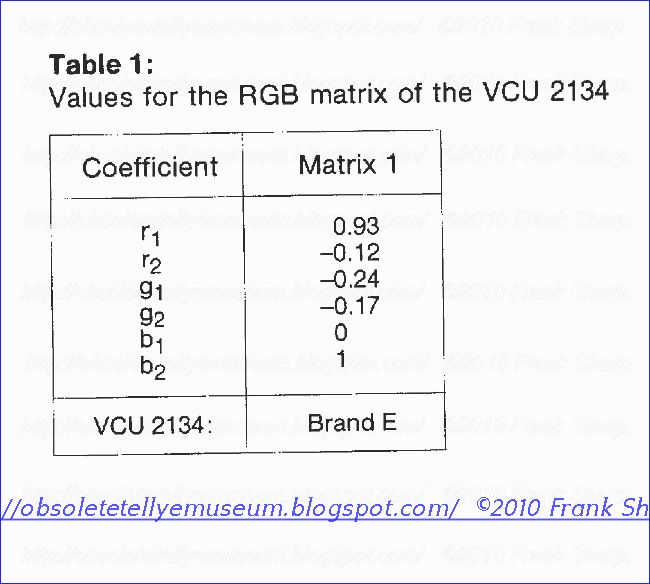
Address no. 16, high byte, bit 6=0 Address no. 16, high byte, bit 5=1: "VHS" mode. Amplification during color burst key x 2 Pin 35: Analog Composite Video, 1.0V max. Pin 37: Analog Composite Video, 1.0V max. Only the data on pin 37 is processed in this mode. Note: The VCU 2136 does not contain the noise inverter that was incorporated in the VCU 2133 any longer. Address no. 16, high byte bit 6 is the former bit "noise inverter”. Changes from the VPU 2203 to the VPU 2204: - on the input side, a demultiplexer was inserted to separate the luma and chroma data in the double data stream and to distribute them into the luma and chroma channels of the VPU (see fig. 3). — the colour trap was conceived to be switched off for the S-VHS operation mode. — Two additional control bits were introduced (refer to the VPU 2203/1E data sheet table 3: "Data transfer between ...”), that is: Address no. 15, low byte, bit 2 "S-VHS on” (see fig. 2): bit 2=0: S-VHS off VPU works on the V1 data only. Luma and chroma data are
separated with the help of chroma trap and chroma filter. bit 2=1: S-VHS on demultiplex of the sequential luma and chroma data, no chroma x 2 during color burst. Address no. 15., low byte, bit 1 (see fig. 3): bit 1=0: chroma trap on. bit 1=1: chroma trap off. New filters in the VPU 2204 To improve frequency response and picture quality some changes in the luminance- and peaking filter part of the VPU have been made. The old filter characteristics are still available. New features are: the S-VHS characteristics without chroma trap the “enhanced” Munakami filter without ringing the “broad” version. For SECAM the broader chroma trap can be switched off to the same chroma trap as for PAL.
DPU 2553, DPU 2554, DPU 2555 Deflection Processors.
During the past few years, digital circuit technology has come into se in television receivers, including color television receivers, for processing the received signal and for generating the deflection signal required to control the movement of the electron beam. During the research for and the development and implementation of these digital circuit systems, the course traced ou by conventional analog signal processing was followed, and the known individual problems were solved by means of digital rather than analog circuits.
By contrast, the present invention is predicated on the realization that, against the background of digital signal processing in television receivers, the constraints resulting from conventional analog technology, particularly with respect to predetermined signal waveforms, can be eliminated, thus making it possible to cope with difficult problems better than with conventional analog and/or digital technology. One of those difficult problems is still the geometric distortions introducted by the nonspherical curvature of the tube screen during reproduction. To eliminate these distortions, a considerable amount of circuitry is required both with conventional analog technology and more recent digital technology; an example is the great number of pincushion-correcting circuits.The fundamental idea of the invention as claimed is to abandon the rigid dependence on the commonly used sawtooth signal for ohorizontal deflection and vertical deflection, which both have a very short retrace period in comparison with the trace period, and to make the individual pixels of the video signal visible on the screen when the two deflection signals have moved the electron beam to the point intended on the transmitter side.
In the present invention, therefore, the deflection signals are no longer generated by a sawtooth generator of long-known analog or more recent digital design, but a deflection processor is provided which generates horizontal and vertical deflection signals with freely selectable waveforms.
The video signal, after being digitized by means of a clock signal, is written into a random-access memory and is read ou in such a way that the individual pixels occupy the intended positions on the screen. The memory has a suitable controller associated therewith, of course. The digital signals read out of the memory must be applied to a compensating stage for correcting picture tube errors before they drive the picture tube via digital-to-analog converters.
Deflection Processors
1.
Introduction These programmable VLSI circuits in N-channel MOS
technology carry out the deflection functions in digital color TV
receivers based on the DIGIT 2000 system and are also suitable for text
and D2-MAC application. The three types are basically identical, but are
modified according to the in- tended application: DPU 2553 —
normal-scan horizontal deflection, standard CTV receivers, also equipped
with Teletext and D2-MAC facility

DPU 2554 -— double-scan horizontal deflection, for CTV receivers equipped with double-frequency horizontal deflection and double-frequency vertical deflection for improved picture quality. At pow- er-up, this version starts with double horizontal frequency.
DPU 2555 — normal scan horizontal deflection as DPU 2553, but with an extra flag for the IM bus, so that one DPU 2553 and one DPU 2555 may be operated simultaneously in one CTV receiver as is required for Teletext or Viewdata operation if increased deflection frequency is intended for high-quality text display. In this case, the DPU 2553 acts as sync separator for the received Teletext or Viewdata signal, whereas the DPU 2555 is used as deflection processor for the displayed page, or viceversa.
1.1.
General Description The DPU 2553/54/55 Deflection Processors contain
the following circuit functions on one single silicon chip: video
clamping horizontal and vertical sync separation horizontal
synchronization normal horizontal deflection east-west correction, also
for flat-screen picture tubes vertical synchronization normal vertical
deflection sawtooth generation text display mode with increased
deflection frequencies (18.7 kHz horizontal and 60 Hz vertical) — D2-MAC
operation mode and for DPU 2554 only: -— double-scan horizontal
deflection - normal and double-scan vertical deflection In this data
sheet, all information given for double-scan mode is available with the
DPU 2554 only.
Types DPU 2553 and DPU 2555 start the horizontal
deflection with 15.5 kHz according to the normal TV standard, whereas
type DPU 2554 starts with 31 KHz according to the double-scan sys- tem.
The
only difference between types DPU 2553 and DPU 2555 is in the function
of the flag IMS which enables and disables the IM bus interface of the
respective deflection processor. With this, it is possible to operate
both types in parallel on the same IM bus, as is required for the
Teletext or Viewdata display mode with increased deflection frequencies.
The following characteristics are programmable: ~ selection of the TV
standard (PAL, D2-MAC or NTSC) - selection of the deflection standard
(Teletext, horizontal and vertical double -scan, and normal scan) —
filter time-constant for horizontal synchronization — vertical
amplitude, S correction, and vertical position for in-line, flat-screen
and Trinitron picture tubes — east-west parabola, horizontal width, and
trapezoidal correction for in-line, flat-screen and Trinitron picture
tubes — switch over characteristics between the different
synchronization modes — characteristic of the synchronism detector for
PLL switching and muting.
1.2. Environment
Fig. 1-1 shows the
simplified block diagram of the video and deflection section of a
digital TV receiver based on the DIGIT 2000 system. The analog video
signal derived from the video detector is digitized in the VCU 2133
Video Codec and supplied in a parallel 7 bit Gray code. This digital
video signal is fed to the video section (VPU, CVPU, SPU and DMA) and to
the DPU 2553/54/55 Deflection Processor which carries out all functions
required in conjunction with deflection, from sync separation to the
control of the deflection power stages, as described in this data sheet.
. Pin Connections

- Ground
- @TMM Main Clock Input
- Output for Single-Scan Vertical Blanking Pulse
- Clamping Output 2
- Reset Input
- Input for the D2-MAC Composite Sync Signal and Output for the Separated Composite Sync Signal
- 1H and 2H Skew Data Output
- Vsup Supply Voltage
- V6 Video Input (MSB)
- V5 Video Input
- V4 Video Input
- V3 Video Input
- V2 Video Input
- V1 Video Input
- VO Video Input (LSB)
- IM Bus Clock Input
- IM Bus Ident Input
- IM Bus Data Input/Output
- Combined Output for the Color Key Pulse and the Undelayed Horizontal Blanking Pulse
- Ground
- Clamping Output 1
- Combined Output for the Delayed Horizontal Blanking Pulse and the Vertical Blanking Pulse
- Horizontal Flyback Input
- Undelayed Horizontal Blanking Output
- Vertical Flyback Safety Input
- Vertical Flyback Output
- Vertical Sawtooth Output
- East-West Parabola Output
- Horizontal Output Polarity Select Input and Start Oscillator Pulsewidth Select Input
- Ground
- Horizontal Output
- Vsup Supply Voltage
- External Standard Selection Input
- Start Oscillator Clock Input
- Start Oscillator Supply Voltage
- Start Oscillator Select Input
- Control Switch Output for the Horizontal Power Stage
- Test Pin, leave vacant
- Interlace Control Output
- Vsup Supply Voltage

2.3. Pin Descriptions
Pins 1, 20 and 30 — Ground These pins must be connected to the negative of the supply.
Pins 2— @M Main Clock Input (Fig. 2-4) By means of this input, the DPU receives the required main clock signal from the MCU 2600 or MCU 2632 Clock Gen- erator IC.
Pin 3 — Single-Scan Vertical Blanking Output (Fig. 2-11) In vertical double-scan mode, this pulse is also required by the CVPU 2235 Comb Filter Video Processor.
Pins 4 and 21 — Clamping Outputs 2 and 1 (Fig. 2-10) These pins supply pulses for clamping the video signal at the VCU 2133 or VCU 2134 during the back porch.
Pin 5 — Reset Input (Fig. 2-2) This pin is used for hardware reset. At low level, reset is actuated, and at high level the DPU is ready for communication with the CCU via the IM bus.
Pin 6 — Input for the D2-MAC Composite Sync Signal and Output for the Separated Composite Sync Signal This pin (Fig. 2-9) is the input for the D2-MAC composite sine signal and the output for the separated composite sync signal.
Pin 7 — Skew Data Output (Fig. 2-10) This pin delivers the 1H and 2H skew data stream required by the PSP 2210 or PSP 2032 Progressive Scan Processor and the TPU 2732 or TPU 2733 or TPU 2740 Teletext Processor or others for adjusting the phase of the double- scan video signal and for information about vertical sync.
Pins 8, 32 and 40 — Vsyp Supply Voltage These pins must be connected to the positive of the supply.
Pins 9 to 15 — V6 to VO Video Inputs (Fig. 2-3) Via these pins, the DPU receives the digitized composite video signal from the VCU 2133 or VCU 2134 Video Codec in a parallel 7-bit Gray code. With a standard signal, the sync pulse resolution is 6 bits.
Pins 16 to 18 — IM Bus Connections These pins connect the DPU to the IM bus. It is via the IM bus that the DPU communicates with the CCU. Pins 16 (IM Bus Clock Input) and 17 (IM Bus Ident Input) have the con- figuration shown in Fig. 2-2. Pin 18 (IM Bus Data Input/Out- put) is shown in Fig. 2-9.
Pin 19 — Combined Output for the Color Key Pulse and the Undelayed Horizontal Blanking Pulse (Fig. 2-11) his output is tristate-controlled. In conjunction with the in- put load represented by the VCU, the three-level key and blanking pulse is produced which is also needed by the other DIGIT 2000 processors.
Pin 22 - Combined Output for the Delayed Horizontal Blanking Pulse and the Vertical Blanking Pulse (Fig. 2-11) This pin is a tristate-controlled output. In conjunction with the input load represented by the VCU, the three-level combined blanking pulse is produced which is also needed by the other DIGIT 2000 processors. Pin 23 — Horizontal Flyback Input (Fig. 2-5) Pin 23 requires horizontal flyback pulses which must be clamped by a diode to the +5 V supply.
Pin 24 — Undelayed Horizontal Blanking Output (Fig. 2-11) This output supplies undelayed horizontal blanking pulses. These pulses are for keying of the IF amplifier and are key- ing pulses for the VCU.
Pin 25 — Vertical Flyback Safety Input (Fig. 2-5) To protect the picture tube from damage by burn-in in the event of a malfunction of the vertical deflection, an ac- knowledge pulse derived from the vertical deflection yoke is fed to pin 25. If this pulse exceeds the 2.5 V threshold during vertical blanking, the blanking pulse will be terminated. If it is planned to operate without this picture tube protection, pin 25 must be connected to +5V.
Pin 26 — Vertical Flyback Output (Fig. 2-12) This pin supplies the same pulse width-modulated sawtooth signal as pin 27, but only for 350 us from the start of the vertical flyback. During the remaining time, pin 26 is at high impedance. The signal supplied by pin 26 is used for fast charge-reversal of the integration capacitor.
Pin 27 ~ Vertical Sawtooth Output (Fig. 2-12) This pin supplies the signal, in pulse width-modulated form, for driving the vertical output stage. To produce the analog sawtooth signal, this signal must be integrated externally, e. g. by an RC network. By way of the IM bus interface and the HSP processor, it is possible for this sawtooth to be varied by the CCU.
Pin 28 — East-West Parabola Output (Fig. 2-12) This pin supplies the vertical-frequency parabola signal for the east-west correction in pulse width-modulated form. Via the IM bus and the HSP processor, the east-west parabola can be adjusted by the CCU.
Pin 29 — Horizontal Output Polarity and Pulse width Select Input (Fig. 2-6) This pin serves for selecting the polarity and the pulse width of the output pulses of pin 31 as described in section 3.4. This pin must be connected to ground or to +5 V.
Pin 31 — Horizontal Output (Fig. 2-10) This output supplies the driving pulses for the horizontal output stage. The output pulse polarity can be selected by means of pin 29.
Pin 33 — External Standard Selection Input (Fig. 2-7) This input is used for selecting the horizontal frequency standard, as shown in Table 3-2. If pin 33 is +5 V, the DPU operates only with the NTSC standard. If it is connected to ground, however, the DPU is set for the PAL or SECAM standard, and the horizontal standard can only be changed by the CCU command between PAL/SECAM and Text dis- play mode. If pin 33 is unconnected, all standards can be selected by the CCU via the IM bus. Furthermore, when pin 33 is unconnected, the horizontal protection circuit is in ef- fect, and for this a 4 MHz signal is required at pin 34. In this case, the output pulse at pin 31 is limited to a maximum du- ration of 30 us for all standards. The phase resolution of the trailing edge of this pulse is reduced to 250 ns, if the output pulse is set to more than 30 ys pulse width.
Pin 34 — Protection Circuit Clock Input (Fig. 2-8) When pin 33 is left unconnected, a 4 MHz clock signal is required at pin 34 for the horizontal protection circuit. The 4 MHz clock can be fed to pin 34 via a capacitor, and is available, e. g., at pin 1 of the CCU at no added cost. If the 4 MHz signal is not present and pin 33 is not connected, the horizontal output pin 31 is undefined.
Pin 35 — Start Oscillator Supply
Via this pin it is possible with minimum current consumption to operate the horizontal protection circuit as a starting oscillator. For this purpose only the 4 MHz signal at pin 34 is required. Pin 36 must be connected to pin 35.
Pin 36 — Start Oscillator Select Input (Fig. 2-6) if the start oscillator function is required (see Table 3-2), pin 36 must be connected to pin 35. If the start oscillator function is not used, pin 36 has to be connected to ground. In this mode, the horizontal output pin 31 is switched off (at high level) as long as the Reset input pin 5 is Low.
Pin 37 — Control Switch Output for the Horizontal Power Stage (Fig. 2-11) This pin serves for switching over the horizontal output
stage to another frequency.
Pin 38 — Test pin This pin is an input/output of the type shown in Fig. 2-9. It is used for testing the DPU during production and should be left unconnected in normal operation.
Pin 39 — Interlace Control Output (Fig. 2-10) This pin is for controlling an AC coupled vertical power stage for interlace-free mode.
3. Functional Description
3.1. Block Diagram
 The
DPU 2553, DPU 2554 and DPU 2555 Deflection Processors perform all tasks
associated with deflection in TV sets: — sync separation — generation
and synchronization of the horizontal and the vertical deflection
frequencies — the various east-west corrections, - vertical sawtooth
generation including S correction as described hereafter. The DPU
communicates, via the bidirectional serial IM bus, with the CCU 2030,
CCU 2050 or CCU 2070 Central Control Unit and, via this bus, is supplied
with the picture-correction alignment information stored in the MDA
2062 EEPROM during set production, when the set is turned on. The DPU is
normally clocked with a trapezoidal 17.734 MHz (PAL or SECAM), or 14.3
MHz (NTSC) or 20.25 MHz (D2-MAC) clock signal supplied by the MCU 2600
or MCU 2632 Clock Generator IC. The functional diagram of the DPU is
shown in Fig. 3-1. 3.2.
The Video Clamping Circuit and the Sync Pulse Separation Circuit The
digitized composite video signal delivered as a 7-bit parallel signal by
the VCU 2133 or
The
DPU 2553, DPU 2554 and DPU 2555 Deflection Processors perform all tasks
associated with deflection in TV sets: — sync separation — generation
and synchronization of the horizontal and the vertical deflection
frequencies — the various east-west corrections, - vertical sawtooth
generation including S correction as described hereafter. The DPU
communicates, via the bidirectional serial IM bus, with the CCU 2030,
CCU 2050 or CCU 2070 Central Control Unit and, via this bus, is supplied
with the picture-correction alignment information stored in the MDA
2062 EEPROM during set production, when the set is turned on. The DPU is
normally clocked with a trapezoidal 17.734 MHz (PAL or SECAM), or 14.3
MHz (NTSC) or 20.25 MHz (D2-MAC) clock signal supplied by the MCU 2600
or MCU 2632 Clock Generator IC. The functional diagram of the DPU is
shown in Fig. 3-1. 3.2.
The Video Clamping Circuit and the Sync Pulse Separation Circuit The
digitized composite video signal delivered as a 7-bit parallel signal by
the VCU 2133 or The DPU has two different clamping outputs, No. 1 and No. 2, one of which supplies the required clamping pulses to the video input of the VCU as shown in Fig. 3-1. The following values for the clamping circuit apply for Video Amp. I. Since the gain of Video Amp. Il is twice that of Video Amp I, all clamping and signal levels of Video Amp II are half those of Video Amp | referred to +5 V. After the TV set is switched on, the video clamping circuit first of all ensures by means of horizontal-frequency cur- rent pulses from the clamping output of the DPU to the coupling capacitor of the analog composite video signal, that the video signal at the VCU’s input is optimally biased for the operation range of the A/D converter of 5 to 7 V. For this, the sync top level is digitally measured and set to a constant level of 5.125 V by these current pulses. The horizontal and vertical sync pulses are now separated by a fixed separation level of 5.250 V so that the horizontal synchronization can lock to the correct phase (
see section 3.3. and Figs. 2-17 and 3-2). With the color key pulse which is now present in synchro with the composite video signal, the video clamping circuit measures the DC voltage level of the porch and by means of the pulses from pin 21 (or pin 4), sets the DC level of the porch at a constant 5.5 V (5.25 V for Video Amp ll). This level is also the reference black level for the VPU 2203, CVPU 2233 or CVPU 2235 Video Processors. When horizontal synchronization is achieved, the slice level for the sync pulses is set to 50 % of the sync pulse amplitude by averaging sync top and black level. This ensures optimum pulse separation, even with small sync pulse amplitudes (see application notes, section 4.).


SPU 2220 SECAM Chroma Processor
SECAM
Chroma Processor Digital real time signal processor for processing
SECAM video chroma signals in combination with the VPU 2203 Video
Processor which processes the luminance information at the same time.
The SPU 2220 is an N-channel VLSI MOS circuit, housed in a 40-pin Dil
plastic package and contains on a single silicon chip the following
functions: — a code converter — a digital SECAM bell filter — a
switchable IF spectrum compensation filter ~ a digital FM de modulator
with DC offset correction, de emphasis and de multiplexer — a digital
Red-/Blue-line identification - a digital standard recognition circuit —
a color saturation multiplier with multiplexer for the color difference
signals — the IM bus interface circuit which provides the communication
with the CCU 2030, CCU 2050 or CCU 2070 Central Control Unit via the
bidirectional IM bus — chroma outputs (pins 23 to 26) can be disabled by
means of pin 22

1. Functional Description
The SPU 2220 digitally processes the SECAM color signals supplied in digital form as a parallel 7-bit Gray-coded signal by the VCU 2133 Video Codec. Acting in parallel with the VPU 2203 Video Processor (Fig. 2),


the SPU 2220 separates the color information from the digital video signal, performs the bell filter function and the IF spectral compensation before submitting the 17.734 MHz sampled signal to the digital algebraic demodulator. The demodulator produces an 8-bit signal, sampled at 4.43 MHz, whose amplitude is proportional to the frequency of the incoming frequency-modulated color difference signal. After demodulation, the color difference signals undergo digital deemphasis before being demultiplexed using a 64 us delay line. After passing the saturation multiplier the co- lor difference signals are multiplexed in a form compatible to that used in the VPU 2203. The SPU 2220 also includes automatic SECAM identification logic as well as Red-/Blue-Line detection and synchronization. Since the signal-
processing delay in the performance of SECAM decoding is greater than that experienced during PAL or NTSC decoding, the SPU 2220 compensates for this delay by delaying the digital video signal supplied to the VPU 2203 by a corresponding amount (5.5 us) in SECAM operation.
1.1. The Code Converter The 7-bit digital video signal supplied by the VCU 2133 Video Codec in the Gray code is initially converted into 7-bit two’s complement binary code for further processing.
1.2. The 5.5 us Delay Line This part of the SPU 2220 delays the digital video signal supplied by the VCU 2133 to be delivered to the VPU 2203. In this way the difference in processing time between the VPU 2203 (luminance channel) and the SPU 2220 (chrominance channel) in SECAM operation is compensated. The color key pulse for the VPU 2203 passes the Aux Delay block of the SPU 2220 in order to provide the same delay as for the video signal delayed in the 5.5 us delay line.
1.3. The SECAM Bell Filter This filter which has the same function as the conventional LC bell filter hitherto used, removes the luminance information and compensates the anti-bell response of the transmitter. Center frequency and frequency response of the bell filter are fixed and cannot be altered externally. The response of the SECAM bell filter is shown in Figs. 3 and 4.
1.4. The IF Spectrum Compensation Filter Since the FM color information in the SECAM system covers a range of frequencies from 3.9 to 4.75 MHz (unlike the single frequency with its AM color information in the PAL and NTSC systems), the slight spectral distortion resulting from the tuner and IF section of the TV set should be compensated. For this, the 14-bit output of the bell filter passes the IF spectrum compensation filter which gives a compensating frequency response of about 4 dB/MHz. This filter can be switched on and off by the CCU via the IM bus using address 107 (see Table 2). Fig. 4 shows the various filter responses of the bell and IF compensation filter with the latter switched on and off.
CVPU 2233 NTSC Comb Filter Video Processor
Article "Color Decoding a PCM NTSC Television Signal" by J. P. Rossi,
Jun., 1974, Journal of the SMPTE, vol. 83, No. 6, pp. 489-495.
Article "Digital Television Image
Enhancement" by J. P. Rossi, 1975, Journal of the SMPTE, vol. 84, at pp.
545-551.
Text "Theory and Application of Digital
Signal Processing" by Rabiner and Gold, (Prentice-Hall, 1975), p. 550.
Paper "Nonrecursive Digital Filters with
Coefficients of Powers of Two" by A. Tomozawa, in the IEEE Int'l. Conf.
on Comm., pp. 18D-1 through 18D-5.
Paper "Colour Demodulation of an NTSC
Television Signal Using Digital Filtering Techniques" by A. G. Deczky,
1975 IEEE Int'l. Conf. on Comm., vol. II, pp. 23-6 through 23-11.
U.S. patent application filed Aug. 31, 1981
in the name of H. G. Lewis, Jr., Digital Color Television Signal
Demodulator, Ser. No.: 297,556.
An Approach to the Implementation of Digital
Filters by L. R. Jackson, reprinted from IEEE Trans. Audio
Electroacoust., vol. AU-16, pp. 413-421, Sep. 1968.
W. Weltersbach et al., "Digitale
Videosignalverarbeitung im Farbfernsehempfanger", Fernseh und
Kino-Technik, 35 Jahrgang, Nr. 9, Sep. 1981, pp. 317-323, (with
translation).
T. Fischer, "Digital VLSI Breeds
Next-Generation TV Receivers", Electronics, Aug. 11, 1981, pp. 97-103.
T. Fischer, "Fernsehen Wird Digital",
Elektronik, No. 16, 1981, pp. 27-35, (with translation of pp. 30-31).
ITT Intermetall, A New Dimension-VLSI Digital TV System, Sep. 1981, pp. 1-23.
In a conventional television receiver, all signals are analog-processed. Analog signal processing, however, has the problems at the video stage and thereafter. These problems stem from the general drawbacks of analog signal processing with regard to time-base operation, specifically, incomplete Y/C separation (which causes cross color and dot interference), various types of problems resulting in low picture quality, and low precision of synchronization. Furthermore, from the viewpoints of cost and ease of manufacturing the analog circuit, a hybrid configuration must be employed even if the main circuit comprises an IC. In addition to these disadvantages, many adjustments must be performed.
In order to solve the above problems, it is proposed to process all signals in a digital form from the video stage to the chrominance signal demodulation stage. In such a digital television receiver, various improvements in picture quality should result due to the advantages of digital signal processing.
NTSC Comb Filter Video Processor Digital real-time signal processor for processing the video signals digitized by the VCU 2133 Video Codec Unit in digital color TV receivers according to the NTSC standard.
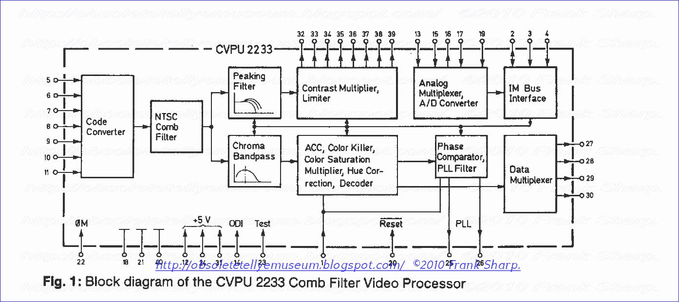
The CVPU 2233 is an N-channel MOS circuit, is housed in a 40- pin Dil plastic package and contains on a single silicon chip the following functions:
— a code converter
— an NTSC comb filter
— the chroma band pass filter
— the luminance filter with peaking facility
— a contrast multiplier with limiter for the luminance signal
~- all color signal processing circuits such as automatic color control (ACC), color killer, identification, decoder and hue correction
~ a color saturation multiplier with multiplexer for the color difference signals
— the IM bus interface circuit for communicating with the CCU 2030 or CCU 2050 Central Control Unit ~ circuitry for measuring dark current (CRT spot-cutoff), white level and photo current, and for transferring this data to the CCU.
1. Functional Description The CVPU 2233 Comb Filter Video Processor digitally processes the digital video signal supplied by the VCU 2133 Video Codec in the various circuit parts just mentioned.


The resulting digital signals are then reconverted to analog signals in the VCU 2133 and used to drive the cathodes of the picture tube, via the external RGB output amplifiers. Further, in conjunction with the VCU 2133, the CVPU 2233 performs a number of measurements and control operations relating to picture tube alignment such as spot-cutoff current adjustment, white level controi, beam current limiting, etc. To understand the signal processing in the two integrated circuits VCU 2133 and CVPU 2233, Fig. 2 may prove useful because it shows the signal flow and the several functional blocks in their logical sequence regardless of whether these blocks are in the VCU 2133 or CVPU 2233.
1.1. The Code Converter This circuit is shown only in Fig. 1. It serves to convert the digitized video signal, delivered by the VCU 2133 in a parallel Gray code, into a simple binary-coded signal for the comb filter.
1.2. The Comb Filter With the NTSC system, a comb filtering for separation of chrominance and luminance signals is easy to realize by a delay line that has the delay of one horizontal period (64 us). In the case of the CVPU 2233, this delay is realized by a RAM. When a comb filter is used, it is no longer necessary to have a chroma trap in the luminance signal path.
1.3. The Luminance Channel The luminance filter has two different values for its band- with, 4 MHz in the case an IF filtered video signal is processed, and 7 MHz if the video signal originates from a camera, a video signal disc player etc. Additionally, the filter handles peaking whereby the high-frequency components of the luminance signal in the range of 3 MHz are raised to improve picture sharpness. The amount of peaking is set by the CCU 2030 or CCU 2050 via the IM bus. Us- ing a fixed subtrahend of —0.25, the sync signal component not required in the luminance channel is suppressed. Peaking at 3 MHz is provided in the range from —3 dB to + 10 dB. It can be set by the user in eight steps. The peaking has a dead-data zone as shown in Fig. 14
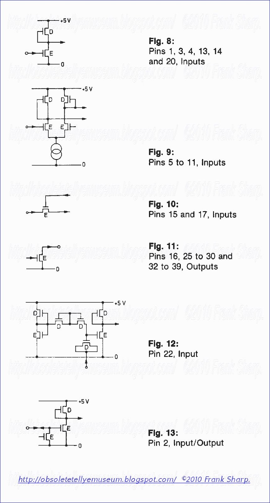
in the description of the VCU 2133. The luminance filter has a DC gain of 1.0 (see Fig. 4). Behind the luminance filter, 9 bits are used to carry the luminance signal, so that the overshoots caused by the peaking filter can be transmitted to the Y D/A converter in
the VCU 2133.
The peaking curves are shown in Fig. 5.
Following the peaking circuit (Fig. 2) is the contrast multiplier which, combined with a limiter, limits the luminance signal if its amplitude becomes too high. The contrast setting, too, is controlled by the CCU via the IM bus, depending on the user’s instructions. Further, the contrast is adapted to the room lighting by means of a photo sensor connected to pin 17 of the CVPU 2233. In this process, the signal generated by the photo sensor is first digitized in the CVPU 2233 and then, during vertical flyback, transferred in multiplex operation to the CCU. The CCU calculates the contrast needed and finally sends the corresponding control signal to the CVPU 2233's contrast multiplier via the IM bus. After the contrast multiplier are added 31 steps as a constant DC signal, so that the system can transmit the negative undershoots-caused by peaking, to the D/A converter (see Fig. 3). From the contrast multiplier, the digital luminance signal is back to 2133 form of a 8-bit signal. In fed the VCU in the VCU 2133,
the signal enters the Y D/A converter. The converter feeds the analog luminance signal to the RGB matrix.
The setting range of the contrast multiplier comprises 6 bits (63 steps) and a gain of 1. If the product of the multiplication at the multiplier’s output is higher than the working range, the largest possible number (1 111 1 1 1 1) is put out. This means the limiting mentioned above is achieved.
4. Inner Configuration of the Connection Pins The following figures schematically show the circuitry at the various pins. The integrated protection structures are not shown. The letter “E” means enhancement, the letter “D” depletion.
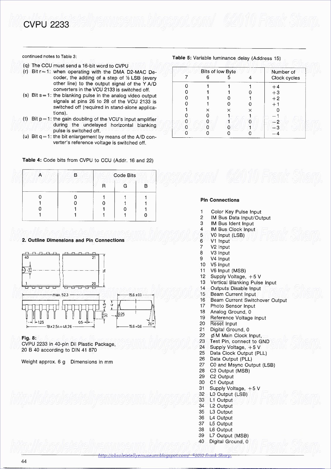

5. Description of the Connections and the Signals
Pin 1 - Color Key Pulse Input This input’s configuration is shown in Fig. 8. Via this pin, the CVPU 2233 gets the color key pulse from pin 19 of the DPU 2543. In the quiescent state high level must be applied, and during pulse a low level.
Pins 2 to 4 - IM Bus Connections By means of these pins, the CVPU 2233 is linked with the CCU 2030 or CCU 2050.
Pins 3 (Ident Input) and 4 (Clock Input) are configured as shown in Fig. 8. Pin 2 (Data Input/ Output) is shown in Fig. 13.
Pins 5 to 11 — Inputs VO to V6 The circuit of these inputs is shown in Fig. 9. Via these in- puts, the CVPU 2233 receives the digitized composite video signal from the VCU 2133 in a 7-bit parallel Gray code. Input VO gets the least significant bit (LSB) and input V6 the most significant bit (MSB).
Pins 12, 24 and 31 — Supply Voltage, +5 V These pins must be connected to the positive of the 5 V supply. Pin 13 — Vertical Blanking Pulse Input Fig. 8 shows the diagram of this input. Via this pin the CVPU 2233 receives the vertical blanking pulse from the DPU 2543. In the steady state, high level must be applied, and during pulse a low level. The vertical blanking pulse is required for controlling the tests described in section 1.5., which are carried out during vertical flyback.
Pin 14 - Outputs Disable Input This input (Fig. 8) serves for fast switch over of the luma and chroma outputs (Pin 27 to 30 and 32 to 39) to the high- impedance state. Pin 14 low means outputs active, and Pin 14 high means outputs disabled.
Pin 15 —- Beam Current Input By means of this pin, whose circuit is shown in Fig. 10, the CVPU 2233 receives the common analog signal which is supplied by three current sensing transistors inserted in the cathode lines of the picture tube. Via the internal switch $1 (Fig. 5) the analog signal is fed to the internal A/D converter. Input voltage range is 0 V to Vig.
Pin 16 — Beam Current Switch over Output This pin serves for selecting the sensitivity of the beam cur- rent input pin 15 by connecting an additional 10 kQ resistor parallel to pin 15 and ground, thus reducing this input’s sensitivity. By this means, the current supplied by the three sensor transistors mentioned is the spot-cutoff current on the one hand (high sensitivity) and the white level current on the other (low sensitivity).
The circuit of pin 16 is shown in Fig. 11.
Pin 17 — Photo Sensor Input This input has the same properties as pin 15. It serves for measuring the current supplied by the photo sensor and is activated by switch S2 (Fig. 5). Its input voltage range is al- so 0 V to Vig.
Pin 18 — Analog Ground, 0 This pin is used as a ground connection in conjunction with pins 15 to 17.
Pin 19 — Reference Voltage Input This pin gets the externally-produced reference voltage of half the supply voltage, that is required by the circuitry shown in Fig. 5 and must be filtered by a capacitor of sufficient capacity.
Pin 20 — Reset Input This pin’s circuit is shown in Fig. 8. In the steady state, high level is required. A low level normalizes the CVPU 2233.
Pins 21 and 40 — Digital Ground, 0 These pins are used as ground connection in all cases where digital signals are invoived.
Pins 22 — gM Main Clock Input Via this pin the CVPU 2233 is supplied with the required main clock signal by the MCU 2600 or MCU 2632 Clock Generator IC. Fig. 12 shows the diagram of Pin 22.
Pin 23 — Test Pin During normal operation, this pin must be connected to ground.
Pin 25 — Data Clock Output (PLL) This pin whose diagram is shown in Fig. 11 supplies the data clock signal needed for the serial data transfer of the PLL information from the phase comparator contained in the CVPU 2233 to the voltage-controlled oscillator (VCO) contained in the MCU 2600 or MCU 2632 Clock Generator IC. The frequency of the data clock signal is one fourth of the main clock’s frequency.
Pin 26 — Data Output (PLL)
This pin whose diagram is shown in Fig. 11 supplies the 12- bit data word explained in section 1.6., which serves for closing the PLL circuit which determines the main clock signal used in the DIGIT 2000 TV receiver.
Pins 27 to 30 — Outputs C3 to CO These outputs’ configuration is shown in Fig. 11. Via these pins, the R-Y, B-Y, and picture tube alignment data is transferred in multiplex operation to the VCU 2133.
Pins 32 to 39 — Outputs LO to L7
These outputs are identical to pin 27, too. Via these pins, the CVPU 2233 delivers the digital luminance signal (Y) to the VCU 2133, where it is reconverted to an analog signal.
VPU 2204
VPU 2204 ,


DTI 2222 2223.
This invention relates generally to digital television systems and specifically to an arrangement for improving the luminance signal transient response characteristics and peaking of a digital television receiver.
A digital television receiver described in the ITT publication entitled "Digit 2000-DSLI Digital TV System," which is incorporated by reference herein, describes a digital color television receiver arrangement having a microprocessor that controls a plurality of function control modules over a so-called IM (Intermetall) bus. The luminance signal processing system of the present invention may be utilized with a television receiver constructed in accordance with the above-mentioned publication.
The art has circuits illustrating transient improvement of video signals to compensate for the effects of limited band-width and the like. In U.S. Pat. No. 4,030,121, issued Jun. 14, 1977, a "video crispener" is disclosed for improving the transient response of vide signals. That system developed first and second differentials of an analog input video signal and processing the first differential through a full wave rectifier and the second differential through a limiting amplifier. The products of the rectifier and limiting amplifier were multiplied and added back to the suitably delayed input video signal. Other variants on the above method were also disclosed. The inventive arrangement of the patent, to Applicants' knowledge has never been implemented in video apparatus.
Peaking of video signals has long been done in television receivers in an attempt to enhance the video display by emphasizing certain frequencies of the video signal. Peaking is arbitrary and is based upon subjective criteria as to what constitutes an optimized display. Conventional analog signal peaking techniques are not useful with digital signals however.
The present invention describes apparatus for processing a digitized luminance signal to accentuate or improve transients in the signal and to selectively and variably peak the signal to emphasize low and high frequencies while controlling undershoot and overshoot of the signal. In accordance with the preferred form of the invention, the various parameters for controlling the amount of peaking and transient improvement are factory settings which may be accomplished in software.
Functional Description 3.1. Block Diagram The DTI 2222 is an N-channel MOS circuit which contains on one silicon chip mainly the following functional blocks (see Fig. 3-1):

- chroma nibble demultiplexer and R-Y/B-Y demultiplexer - R-Y and B-Y interpolation filters - R-Y and B-Y rise time detectors - hold pulse generator - chroma nibble multiplexer - clock generator and MUX/DEMUX control - luminance delay circuit - IM bus interface The normal risetime of Luminance transients is about 150 ns, how- ever, for chrominance transients the rise time is between 800 and 1000 ns. The picture impression, especially of color bars in the standard test pattern, is considerably improved if the chrominance transients are given the same short rise time as the luminance transients.
TPU 2732
Teletext
Processor for Level 1 Teletext The TPU 2732 is specified to handle
Level-1-Teletext information (in Germany: Video text) as it is
transmitted today by the TV broadcast stations in Great Britain, Germany
and other European countries. In this function, the TPU 2732 is part of
the DIGIT 2000 digital TV system and works in con- junction with the
other VLSI circuits and processors of this system. The Teletext adapter
designed with the TPU 2732 is very simple and economic (Fig. 1), so that
this new fea- ture may now become common as it was not possible due to
the high cost of former multi-chip solutions up to now.

The TPU 2732 is an N-channel VLSI MOS circuit, housed in a 40-pin Dil plastic package and contains on a single silicon chip the following functions:
— one-chip solution of the Teletext processing (except for external RAM)
— ghost compensation to eliminate the effects of ghost pictures due to reflections
— as input signal is used the 7-bit digitized composite video signal delivered in a parallel Gray code by the VCU 2133 or VCU 2134 Video Codec
— reduced access time is provided for the Teletext pages by receiving and storing up to eight pages in one go
— up to eight stored pages
— function extended by automatic language-dependent character selection
~ switchover facility PAL/NTSC TPY 2732 H for Hebrew Characters Using the type designation TPU 2732 H, a mask option of the TPU 2732 can be supplied which, instead of the automatic language-dependent character selection described in sections 9.7. and 10.3., only displays the Hebrew character set.
With this device, the language-selecting control bits Cy to C14 or LSO to LS2 have no effect. 1. Short Functional Description The TPU 2732 whose block diagram is shown in Fig. 2, op- erates according to a rigid timing determined by the vertical cycle of the TV receiver. The data acquisition period starts at line 7 with PAL or line 10 with NTSC and ends at line 22 with PAL or line 21 with NTSC. During this period, the input data is processed by a ghost filter which is able to compensate reflections with short delay time of 0 to 0.8 us for PAL or 0 to 1 us for NTSC. Teletext information is synchronized and identified. A comparator pre selects the pages with page numbers that are requested by the CCU 2030, CCU 2050 or CCU 2070 Central Control Unit and loads them into the RAM. To eliminate speed problems of the external RAMs, the data is buffered in an internal RAM buffer (Fig. 2). The comparator contained in the data acquisition unit decides into which sector of the RAM the data is stored. The display period
starts at line 48 with PAL or line 50 with NTSC and ends at line 286 with PAL or line 242 with NTSC. The display control unit selects one of the stored eight pages for display. The 8-bit character words are trans- formed into a 6 x 10 dot matrix with PAL or 6 x 8 dot matrix with NTSC by a character generator (ROM) of 96 programmed characters and are displayed in 24 rows of 40 characters each. Different character sets are available for eight languages under CCU or transmitter control, the required character set being selected automatically by the control bits C1 to C14 of row O of the Teletext page display- ed. Every tenth line with PAL or every eighth line with NTSC a new Teletext row is loaded from the RAM into the RAM buffer. When the RAM is not.accessed by the TPU 2732, the memory control refreshes the memory and handles CCU requests for RAM access. Via the IM bus the CCU can read from and write into ail RAM locations and controls the TPU 2732 by loading the appropriate registers in the RAM, so that the
TPU 2732 can be used to display text from other sources. The TPU 2732 can display a list of contents of the stored eight pages (me- nu) all by itself. As external RAM can be used either one 64 K x 1 bit Dynamic RAM or one 16 K x 1 bit Dynamic RAM. So, the RAM capacity is flexible to store 2 or 8 pages. The RAMs can be standard types (see section 3.).
 MCU 2600 Clock Generator IC
Clock
Generator IC Integrated circuit in Cl technology for generating the
main clock @M for digital TV receivers according to the DIGIT 2000
concept.
1.
Introduction The MCU 2600 Clock Generator IC supplies the digital
signal processors, decoders, converters etc. of the DIGIT 2000 digital
TV system with the required main clock signal, which is of trapezoidal
shape, with rounded corners, in order to avoid interference.
For PAL
and SECAM, the clock frequency is four times the PAL color subcarrier
frequency, and for NTSC, the clock frequency is four times the NTSC
color subcarrier frequency: for PAL and SECAM: fom=4 x 4.4383 618 75
MHz= 17.734475 MHz for NTSC: fom=4 x 3.579545 MHz= 14.318 180 MHz for
D2-MAC: fg. =20.25 MHz
2. Functional Description As can be seen from the block diagram Fig. 2-1,


three VCOs (voltage-controlled oscillators) integrated in the MCU 2600 Clock Generator IC (one for PAL and SECAM, one for NTSC, and one for D2-MAC operation) form part of a PLL (phase-locked loop) circuit, the other parts of which, the phase comparator and the digital PLL filter are placed in the VPU 2203 or the CVPU 2233 or the CVPU 2235 or the DMA 2270. The filtered phase difference signal Ag is sup- plied in digital serial form (Fig. 2-2) to pin 6 of the MCU 2600. This data transfer is controlled by means of the data clock signal which is fed to pin 5 of the MCU 2600 and whose frequency is % of the main clock signal @M. With the negative transition of the data clock signal, the data is written into the shift register, and with the positive transition, the content of the shift register is shifted by 1 bit. After 12 bit have been written into the shift register and the data clock signal has attained again the stable high level (Fig. 2-2), an internal delay of about one data clock period occurs.
This following, the data are taken over into the parallel register. From there, the information is fed to the oscillator control circuit and to the 9-stage D/A converter that produces the tuning voltage for the three voltage-controlled oscillators. The write-and-store cycle is initiated at the begin of each horizontal sweep. The closed control loop ensures a phase-true locking be- tween the oscillator signal (from which is produced the @M main clock) and the color subcarrier burst or the digital data burst contained in the received signal. The signal produced by the VCO in action, is transferred to the filter via the oscillator control circuit. The filter forms the required main clock @M and is followed by the output buffer that provides a low-impedance output signal suited for clocking the DIGIT 2000 signal processors. The timing of the data transfer from the VPU 2203, CVPU 2233 or CVPU 2235 Video Processor or the DMA 2270 D2-- MAC Decoder to the MCU 2600 Clock Generator IC is illustrated in Fig. 2-2. The
first three bits serve for selecting the required VCO, depending on whether PAL/SECAM, NTSC, or D2-MAC operation is chosen. The following nine bits (LSB first) provide the tuning signal for the VCO in the shape of two’s complement. These nine bits are composed of the filtered sign-containing phase deviation Aq (7 bits) and the sign-containing alignment value for the oscillator (8 bits). If the MCU 2600 Clock Generator IC is employed in a multi- standard TV set, the required VCO is selected in the way al- ready described. For use in a single-standard receiver, the selection of the operating VCO is free and independent of the data signal. The not-used oscillators can be blocked externally by applying ground to pins 9, 10 or 12. In the case of a multi-standard TV set with up to three operated VCOs, the priority level for operation is internally fixed with the highest level for VCO 1 and the lowest level for VCO 3. This means, when switching on and also in the case of data faults the oscillator control circuit
will select the oscillator with the highest level, if the input of this oscillator is not externally grounded. It should be noted that all connection rails on the PC board must be designed under the point of view of HF signals. An inductance of 10 nH/cm can be assumed at a 0.5 to 1 mm wide rail. This makes an inductive impedance of several Ohms per cm length for the important 3°¢ harmonic of f gy. Best performance is given by ground plane layout of the PC board. All ground and signal lines should be as wide as possible, inductance-free and without loops in the neighbourhood of high HF currents. All supply pins of the clock generator IC must be equipped with ceramic bypass capacitors directly at the IC to ground pins on the shortest possible way.
6. Description of the Connections and Signals
Pin 1 — Ground of Output Buffer This pin serves as separate ground pin for the output buffer and must be carefully decoupled from the crystal oscillators and the input signals.
Pin 3 —- @M Main Clock Output (Fig. 5-1) This pin supplies the clock signal for the DIGIT 2000 TV receiver for clocking all signal processors used in this system.
Pin 4 — Vsyp Output Buffer Supply A positive supply voltage of 5 V is required which powers the output buffer and must be well decoupled with respect to the other supply pin. For this, a bypass capacitor is required between pins 4 and 1.
Pin 5 — PLL Clock Input (Fig. 5-2) Via this pin the MCU 2600 Clock Generator receives the PLL clock for transferring the tuning signal from the VPU, the CVPU or the DMA to the VCO integrated in the MCU 2600.
Pin 6 — PLL Data Input (Fig. 5-2) The desired oscillator is selected by the signal fed to pin 6 as described in Table 4-1. Additionally, pin 6 receives the digital PLL information supplied by the VPU, the CVPU or the DMA, to control the VCO included in the MCU 2600 Clock Generator.
Pin 7 — Ground This pin serves as ground pin for the whole circuit except the output buffer. Its connection should be separated care- fully from the pin 1 ground connection.
Pins 8 to 13 — Crystal Connections (Fig. 5-3) In addition to the oscillator function, the respective input pin serves also for switching off the not-used oscillators by connecting their input pins to ground (pin 7).
Pin 14 — Vgyp Supply Voltage This pin is the supply pin for the whole IC except the output buffer. It must be decoupled carefully with respect to the output buffer supply pin 4. For this, a bypass capacitor between pins 14 and 7 is required.
MDA 2062 1024-Bit EEPROM
1024-Bit EEPROM
Electrically erasable programmable read-only memory (EEPROM) in N-channel floating-gate technology with a capacity of 128 words, 8 bits each. The MDA 2062 is intended for use as a re programmable non-volatile memory in conjunction with the CCU 2030/2050/2070 series Central Control Units of the DIGIT 2000 Digital TV System, the MAA 4000 Remote-Control and PLL-Tuning Microcomputers for TV receivers or the SAA 1280, SAA 1290 and SAA 1293 Remote-Control and Tuning ICs. It serves for storing the tuning information as well as several analog settings, further alignment information given in the factory when producing the TV set. The stored information remains stored even with the supply voltages switched off. Reading and programming operations are executed via the IM bus (see section 7.). Input and output signals are TTL level. An address option input provides the possibility to operate two memories in parallel, to obtain a total storage capacity of 2048 bits.

1. Functional Description
1.1. Memory Operation
The internal memory address space ranges from address 128 to address 255. Addresses 4 and 14 provide special functions. To read a stored data word, the desired memory address has to be entered to the memory address register first. This is done by serially entering the IM bus address 128 (optionally 132) (during Ident = L), followed by the memo- ry address (during Ident = H) in a single IM bus operation. With the memory address register set, the memory data may be read. This, in turn, is done by entering the IM bus address 129 (optionally 133) to the device (during Ident = L). Immediately after this, within the same IM bus operation (during Ident = H) the open-drain Data output will conduct to serially transmit the respective 8-bit memory data. Reprogramming a memory location is done in two steps, a) and b), that are identical except for the data word to be entered. Step a) resets all bits to “1”, and step b) programs the desired data into the selected memory location. a) First, the desired memory address is
entered in the way described above. Second, the actual programming is initiated by serially entering the IM bus address 131 (optional- ly 135) followed by the data word to be stored, which is 255 for step a). The device will now internally time its program- ming sequence of approx. 16 periods of the 1 kHz memory clock. During this “busy” time all inputs are blocked from affecting the programming except for the Reset input. A Reset = L signal will immediately cancel any programming operation as well as any bus operation in progress. The busy state may be interrogated by reading bit 1 of ad- dress location 14. A high level of this “busy-bit” indicates that programming is still under way. The IM bus operation for entering address 14 should always directly precede reading the busy-bit. Reading any other address location during the busy state will produce erroneous data at the Data output. An address change operation during the busy state will not change the memory address register content. The intended start of another programming operation during the busy time will not be executed. b) After time-out, normal operation may be resumed, e. g. by performing the second step of a programming sequence, i. e. by programming the desired 8-bit data word into the respective memory address location. This is done by restoring the proper memory address first, if necessary, and then by serially entering the IM bus address 131 (optionally 135) followed by the desired 8-bit data word. The device will again time its own programming sequence as described under a). After time-out the new data may be verified.
1.2. Redundancy
The MDA 2062 EEPROM contains circuitry that allows to replace up to two rows of the memory matrix, each containing 4 bytes of memory, by redundant rows SR 1 and SR 2. This substitution can be done in the field, by the user. To prepare for activation of SR 1, memory address location 192 must contain the 5 LSB of the memory address containing the defect, which identifies the row to be substituted. Furthermore, bit 5 has to be set to “0”, which identifies the data to be redundancy relevant (see Fig. 2). To prepare for activation of SR 2, memory address location 160 must contain the equivalent data.
The activation itself of the redundant rows is done by reading the content of memory address locations 192 and 160. This transfers the repair information stored nonvolately in the memory array to volatile repair registers. It is important to note that the repair registers are cleared (bit 5 set to “1”) by any Reset = L signal. Thus, any LH transition of the Reset signal must immediately be followed by reading the memory address locations 192 and 160, which restores the repair information to the repair registers. SR 2 may be substituted by SR 1, whereas SR 1 cannot be substituted. As well, row 0 which contains the memory address locations 192 and 160 cannot be substituted. SR 1 and SR 2 are part of the memory matrix portion that is not protectable by the S signal. Memory address locations 192 and 160 are part of the protectable portion.
1.3. Testing The MDA 2062 EEPROM contains circuitry designed to facilitate testing of the various functions. By programming data into address location 4, the device is switched to one or more of a number of test modes. A detailed description is given in section 6.
1.4. Protected Matrix The programming matrix contains a protectable portion. Addresses 128 to 134, 160 to 166, 192 to 198 and 224 to 230 can only be programmed if the “Safe” input S (pin 6) is at high potential. In that way, this portion of the memory is protected against inadvertent reprogramming even if such false information were received via the IM bus. The second part of the programming matrix is not protected.
1.5. Shipment Parts are shipped with all bits set to “1”, except for ad- dresses 192 and 160 which may contain repair information. The content of memory address locations 192 and 160, if different from 255, should not be altered, as this will result in defective rows appearing within the memory address space.
5. Description of the Connections and the Signals
Pin 1 — Option Input Fig. 5 shows the internal configuration of this input. With Pin 1 at ground potential (low) or floating, the MDA 2062 reacts upon the IM bus addresses 128, 129 and 131. With pin 1 continuously at Vpp potential (high), the MDA 2062 reacts upon this IM bus addresses 132, 133 and 135 (see Fig. 8). In this way, parallel operation of two MDA 2062 is permitted, to obtain 2048 bits of non-volatile storage direct- ly accessible via the IM bus. Pin 1 is internally tied to ground via a transistor equivalent to a 40 kQ resistor.


Pins 2, 4, 5 and 11 — NC These pins are not connected internally.
Pin 3 — Programming Voltage Vp A programming voltage of + 20 V (+ 5%) is required. The current consumption during programming is approximately 1 mA. During non-programming operations, pin 3 may be held at any level between (Vpp — 0.7 V) and + 21 V. It may also be left floating. The MDA 2062 EEPROM must not be inserted or removed from a socket with Vp > 6 V. During power on/off sequences, current from the Vp supply should be limited to Ip max = 5 MA.
Pin 6 ~ Safe Input S Fig. 5 shows the internal configuration of this input. Normally, with pin 6 at ground potential (low), one portion of the programming matrix is protected so that this part of the memory cannot be reprogrammed inadvertently. Only when pin 6 receives high potential continuously, the protected portion of the memory matrix can be programmed. Pin 6 is internally tied to ground via a transistor equivalent to a 40 kQ. resistor.
Pin 7 — Ground, 0 This pin must be connected to the negative of the supplies.
Pins 8 to 10 — IM Bus Connections These pins serve to connect the MDA 2062 EEPROM to the IM bus (see section 7.), via which it communicates with the CCU 2030/2050/2070 or MAA 4030 series pC or the SAA 1280/SAA 1290/SAA 1293.
Pins 8 (IM Bus Clock In- put) and 9 (IM Bus Ident Input) are inputs as shown in Fig. 6 and pin 10 (IM Bus Data) is an input/output as shown in Fig. 7. The signal diagram for the IM bus is illustrated in Figs. 8 and 11. The required addresses which the MDA 2062 EEPROM receives from the microcomputer, are also shown in Fig. 8.

Pin 12 — Reset Input This input has a configuration as shown in Fig. 6. Via this in- put, the MDA 2062, together with the other circuits belong- ing to the system, receives the Reset signal which is derived from Vpp via an external RC circuit. A low level is required during power-up and power-down procedures. Low level at pin 12 (max. 1.3 V) cancels a programming procedure and an IM bus operation in progress.
The memory address register is not, the repair register is erased.
During operation, pin 12 requires high level (min. 2.4 V). Pin 13 — Memory Clock Input Via this input (Fig. 6) the MDA 2062 receives a 1 kHz clock signal from pin 3 of the CCU 2030, CCU 2050, CCU 2070 or MAA 4030 microcomputer or the SAA 1280/SAA 1290/SAA 1293.
Pin 14 — Supply Voltage Vpp
The supply voltage required is + 5 V (+ 5 %), and the current
consumption in active operation is approx. 30 mA.
6. Test Functions
This description of the test byte is not part of the specification. It contains no information necessary for normal (intended) use of the MDA 2062 memory. It is only intended as a description of the various functions of the test byte that are designed for factory use, but it does not specify such properties. The description is subject to change. Address location 4 contains a test byte which governs test mode operation of the MDA 2062. The test byte is set by performing the IM bus operation for entering address 4, followed by an IM bus programming operation with the desired test data word.
The test byte is valid during all following IM bus operations until changed or set to 0 by a Reset = L signal. The test byte shall not be changed during the busy time of a programming operation. Fig. 9 shows the bit arrangement of the test byte. Set bit 5 for activation of the test byte!
Block Programming Three block program modes can be activated by the test byte, in conjunction with the memory address loaded into the memory address register: 1) all bytes are selected (including 8 bytes in redundant rows): 2) all even-numbered bytes are selected (redundant bytes are not predetermined, they have to be defined as even bytes): 3) all odd-numbered bytes are selected (redundant bytes are not predetermined): memory address 76543210 1xxxxxOx (e.g. 128) 1xxxxx10 = (e.g. 130) 1xxxxx11~= (e.g. 131)
Thus, programming all selected bytes with the same de- sired data is done within one programming sequence. The complete sequence is: Enter Address 4 Program Test byte (e. g. 160) Enter Address 128, 130 or 131 Program Data A checker board pattern is programmed with two program- ming operations after loading the test byte: Enter Address 130 Program Data 85 Enter Address 131 Program Data 170 Read Reference Shifting
During read operations the memory cell threshold voltage is compared with a reference voltage. The comparator out- put then produces the logic one level for a cell threshold higher than the reference and the logic zero level for a cell threshold lower than the reference. The test byte provides means to shift the reference voltage in positive or negative direction in three steps: +0.3V, +06Vand + 09V.
During a read operation a positive-shifted reference voltage establishes a margin test for logic ones, whereas a negative-shifted reference does so for logic zeroes. This margin test is performed digitally by IM bus operations on- ly, without the need to switch analog power supplies. +0.9V: +0.6V: +0.3V: -—-03V: —06V: —~0O9V: 76543210 ~x010x1x1 x010x0x1 x010x1x0 *x110x0x0 x011x0x0 ‘%~111x0x0
Redundancy Disable
With bit one of the test byte set, the redundant rows can be accessed neither during byte program operations nor during any read operation, even if the redundancy registers are properly loaded. This test byte function has no effect on block programming operations.
Ramp Disable
The MDA 2062 contains circuitry to shape the internal program supply voltage to be a ramp function during programming operations. This feature is considered to be essential to a high erase/write endurance of the memory cells. Bit 3 of the test byte disables this ramp function so that the internal program supply, according to the timing diagram Fig. 10, is immediately disconnected from the Vop supply and connected to the Vp supply at the 4th falling edge of the 1 kHz memory clock, and is immediately disconnected from the Vp supply and re-connected to the Vpp supply at the 14th falling edge of the 1 kHz clock after the last rising Ident signal edge of the IM bus operation starting the program cycle. By this feature other than the built-in ramp function (approx. 100 ts/V) can be applied via the Vp supply pin.
7. Description of the IM Bus
The INTERMETALL Bus (IM Bus for short) has been designed to control the DIGIT 2000 ICs by the CCU Central Control Unit. Via this bus the CCU can write data to the ICs or read data from them. This means the CCU acts as a master whereas all controlled ICs are slaves. The IM Bus consists of three lines for the signals Ident (ID), Clock (CL) and Data (D). The clock frequency range is 50 Hz to 170 KHz. Ident and clock are unidirectional from the CCU to the slave ICs, Data is bidirectional. Bidirectionality is achieved by using open-drain outputs with On-resistances of 150 2 maximum. The 2.5 kQ pull-up resistor common to all outputs is incorporated in the CCU. The timing of a complete IM Bus transaction is shown in Fig. 11 and Table 1. In the non-operative state the signals of all three bus lines are High. To start a transaction the CCU sets the ID signal to Low level, indicating an address transmission, and sets the CL signal to Low level as well to switch the first bit on the Data line. Thereafter eight address

bits are transmitted beginning with the LSB. Data takeover in the slave ICs occurs at the High levels of the clock signal. At the end of the address byte the ID signal goes High, initiating the address comparison in the slave circuits. In the addressed slave the IM bus interface switches over to Data read or write, because these functions are correlated to the address. Also controlled by the address the CCU now transmits eight or sixteen clock pulses, and accordingly one or two bytes of data are written into the addressed IC or read out from it, beginning with the LSB. The Low clock level after the last clock pulse switches the Data line to High level. After this the completion of the bus transaction is signalled by a short Low state pulse of the ID signal. This initiates the storing of the transferred data. It is permissible to interrupt a bus transaction for up to 10 ms.
ADC 2310 E Audio A/D Converter
Audio A/D Converter
1. Introduction
Analog-to-digital
converter for digitizing the analog stereo sound signals in digital TV
receivers based on the DIGIT 2000 system, intended for working together
with the APU 2400 T or the APU 2470 Audio Processor, being controlled by
the CCU 2030, CCU 2050 or CCU 2070 Central Control Unit and being
clocked by the MCU 2632 Clock Generator. The ADC 2310 E is an integrated
circuit in Cl technology, housed in a 24-pin Dil plastic package, and
contains on one silicon chip the following functions (see Fig. 1-1):

— several analog input and output amplifiers
— five analog switches (S1 to $5) for selecting different
signal sources
— an analog stereo dematrix circuit
— alevel control facility
- two pulse-density modulators (PDM | and PDM Il)
— an IM bus interface
2. Functional Description Fig. 2-1 shows the block diagram of a digital stereo sound channel intended for a DIGIT 2000 TV receiver, equipped with additional audio inputs and outputs which can be used with the so-called Euro connector or SCART connector, e. g. for connecting a video recorder.
The analog sound signals selected for conversion by the analog switch S1 firstly pass through the level control section where the desired level control is carried out. Thereafter, they are fed to the first processing stage of the A/D conversion, the pulse-density modulators PDM | and PDM Il, whose output signals are 1-bit data streams with a data rate of 4.7 MHz maximum. This data is then transferred to the APU Audio Processor where the digital decimation filters are the input, performing the second step of the con- version process. Due to the very high sampling rate of the pulse-density modulators, no steep anti-aliasing filters are needed at the input. The digital output data of the whole converting system has a signal-to-noise ratio which can be compared to that of a conventional 13-bit A/D converter.
The TV Audio inputs get their analog signal (_+R and 2 R) from the stereo decoder of the TV set, whereas the Aux. Analog inputs are intended to receive an audio signal from a video recorder or another external source, e.g. via the SCART connector. The Analog Out | and II pins supply the selected audio signal, e.g., to the SCART connector for connection to a video recorder or other equipment.
2.1. The Analog Switches The five analog switches S1 to S5 (S1 and S3 are two-pole switches) are controlled via the IM bus (see section 2.6.) to select the required connections between the four analog inputs and the two digital outputs and the two additional analog outputs.
2.2. The Dematrix When switched on via the IM bus (switch 2, see Table 2-2),


the dematrix provides the 2 R and 2L stereo signals at the analog outputs. These signals are extracted form the L+R and 2R input signals according to the German TV stereo sound system (see Table 2-1 ).
2.3. The Pulse-Density Modulators The two pulse-density modulators, PDM | and PDM Il, are sigma-delta modulators equipped with two feedback loops each. At the outputs they supply pulse trains whose pulse density is proportional to the amplitude of the input signal. The maximum sampling rate, and thus the maximum pulse rate, is 4.7 MHz. possibilities are switched off, the capacitor at pin 9 is discharged rapidly to 2.8 V, and the level control goes to full level. The level control is under IM Bus control as shown in Table 2-2.
2.4. The Level Control Section This part of the ADC 2310 E serves to reduce the level of the input signal to be converted if the input signal exceeds the level for full drive of the PDM pulse-density modulators. Controlled by the IM bus, the audio level is sensed either in channel | or in channel fl or in both channels. If all three possibilities are switched off, the capacitor at pin 9 is discharged rapidly to 2.8 V, and the level control goes to full level. The level control is under IM Bus control as shown in Table 2-2.
2.5. The Clock Divider This part of the ADC 2310 E is provided for adapting the digital stereo sound channel to different TV standards. With bit 7 = Low (see Table 2-2 ), the divider ratio is set to 4:1, whereas bit 7 = High gives 3:1. This allows operation of the ADC 2310 E with almost the same sampling frequency at a main clock frequency OM of 17.7 MHz (PAL) or 14.3 MHz (NTSC), both supplied by the MCU 2632 Clock Generator.
2.6. The IM Bus Interface This circuit section is provided for controlling the ADC 2310 E by the CCU 2030, CCU 2050 or CCU 2070 Central Control Unit via the IM bus (see section 7.). In the case of ADC 2310 E, the IM bus is unidirectional from the CCU to the ADC. That means that information is only transferred from the CCU to the ADC 2310 E. The bit arrangement is shown in Fig. 2-2, and the actions performed can be de- rived from Table 2-2.
2.7. The Preemphasis and Deemphasis
The audio signal supplied by the stereo decoder or video demodulator of the TV set has a preemphasis determined.
5. Description of the Connections and Signals
Pin 1 — Ground
(Analog) This pin serves as ground connection for the analog input signals at pins 4, 5, 8, 21 and 24 and as ground connection for the supply of the analog part of the ADC 2310 E.
Pins 2, 3, 6 and 7 — Capacitor Pins (Fig. 4-8) The filter capacitors for the inner and the outer feedback loop of the pulse-density modulators PDM | and PDM II must be connected to these pins.
Pins 4 and 5 — Analog (TV) Audio Inputs | and I! (Fig. 4-1)


These two inputs get their input signal from the stereo decoder or sound demodulator of the TV set, coupled via capacitors. The input signal range can be increased by adding series resistors.
Pin 8 — Analog (TV) Pilot Input (Fig. 4-2) It is possible to supply the ADC 2310 E with the pilot regardless of the position of switch S1 via this pin. The signal must be coupled capacitively.
Pin 9 ~ Level Control RC Pin (Fig. 4-9) The RC element connected to this pin determines the response time of the level control circuit.
Pins 10 and 11 — PDM Digital Sound Outputs (Fig. 4-5) These pins are the outputs of the pulse-density modulators PDM | and II which supply the PDM data to the APU Audio Processor.
Pin 12 —Vgyp; Supply Voltage (Analog) The analog circuitry of the ADC 2310 E is supplied via this pin.
Pin 13 —- Vgype Supply Voltage The supply at this pin powers the analog switches.
Pin 14 — Ground (Digital)
This pin is the ground connection for the digital output signals supplied by pins 10 and 11 and for the supply of the digital part of the ADC 2310 E.
Pin 15 — @M Clock Input (Fig. 4-3) This pin receives the required clock signal from the MCU 2632 Clock Generator.
Pin 16 — Bit 6 Data Output (Fig. 4-6) This output provides the status of bit 6 (see Table 2-2).
Pins 17 to 19 ~ IM Bus Inputs (Fig. 4-4) The ADC 2310 E is connected to the IM Bus and receives commands issued by the CCU via these pins.
Pin 20 — Vgyp; Supply Voltage (Digital) Pin 20 supplies the digital part of the ADC 2310 E.
Pins 21 and 24 — Analog (Aux) Audio Inputs | and Il (Fig. 4-2) These inputs can be used as playback inputs from a video recorder or other external sources, e. g. connected via the Euro or SCART connector. The input signal must be coupled via capacitors. The input signal range can be in- creased by adding series resistors.
Pins 22 and 23 —- Analog Audio Outputs | and II (Fig. 4-7)
These two analog outputs provide either the signals of the TV inputs (pins 4 and 5) or the signals of the Aux inputs pins 21 and 24, depending on the state of the analog switches which are set by the CCU via the IM bus according to Table 2-2.
APU2470 Audio Processor
digital Audio Processor
1. Introduction
The APU 2470 Audio Processor is an N-channel MOS circuit, housed in a 24 pin Dil plastic package. It is designed to perform digital processing of TV audio information. The architecture of the APU 2
 470 combines two main blocks:
1/0 blocks DSP block The I/O blocks are used to manage the input and output of audio information. The DSP block consists of a mask-programmable digital signal processor, whose software can be controlled by a microprocessor (CCU) via the IM bus. So parameters like coefficients can be modified during performance. By means of the DSP software, audio functions like dematrixing, bilingual mode, tone manipulation and volume control are performed. To allow bilingual performance two audio processing channels are available: MAIN channel, provided for the loudspeaker system AUX channel, provided for headphones Fig. 1-1 gives an overview of the APU functions.
1.1. Application of the APU 2470 The APU2470 is designed to interface with ITT’s ADC 2310E Audio A/D Converter as well as with the DMA 2270 D2-MAC Decoder or the NIP 2400 NICAM Demodulator/Decoder and the AMU 2485 Audio Mixer. It can receive digital data in two different formats:
a) The ADC 2310E receives analog audio information either from the SCART Interface, also called Euro connector (for example: video recorder) or from any terrestrial TV transmission and converts it into two 1-bit PDM streams. For this input format, decimation filters are provided in the APU 2470, converting each PDM stream into a 16-bit word at a sampling rate of approximately 35 kHz.
b) Digital serial audio data, provided for example by the DMA 2270 D2-MAC Decoder or the NIP 2400 NICAM Demodulator/Decoder and mixed in the AMU 2485 Audio Mixer, can be received via the S bus by means of the S bus interface.
ITT’s CCU 2030, CCU 2050, CCU 2070 or CCU 3000 Central Control Units of the DIGIT 2000 family are well suited for interfacing with the APU 2470 Audio Processor. Fig. 1-2 shows how the APU 2470 can be used together with the mentioned ITT ICs to realize multistandard audio processing with PAL and D2-MAC or NICAM signals. In the follow- ing descriptions data coming from the ADC will be called “PDM-Data’”, and data from the AMU will be called “S-Data”. Two different audio configurations are possible with the APU 2470 (Fig. 1-2). The dashed line version uses the AMU 2485 as a pre processing unit both for PDM-Data and S-Da- ta and allows mixing between both kinds of inputs. Another advantage of this version is the digital 50 us deemphasis included in the AMU 2485 applied to the PDM inputs. This gives the flexibility to switch between the D2-MAC/NICAM J17 deemphasis and the FM 50 us deemphasis without using analog means. This version is recommended for new TV concepts. The other application needs an analog 50 us
deemphasis in case of S-Data input in the AMU 2485. For that reason a switchable 50 us preemphasis is included in the AMU 2485. This version can be used in conjunction with the old ADC-APU concept.

5.3. Pin Descriptions
Pins 1 and 21 — Reference Current Inputs (Fig. 5-2) These inputs require a current of 150 uA called reference current Ine- and serving for volume adjustment in the DAC interfaces.
Pins 2 and 12 — Digital Ground, 0 These pins must be connected to the negative of the supply. They have to be used for ground connections in con- junction with digital signals.
Pins 3, 4 and 5 — IM Bus Connections
Via these pins, the APU 2470 is connected to the IM bus and communicates with the CCU. Pins 4 (IM bus Ident input) and 5 (IM bus Clock input) have the configuration shown in Fig. 5-3. Pin 3 (IM bus Data input/output) is shown in Fig. 5-7. The IM bus is described in section 2.1.3.
Pins 6, 8, 9 and 15 — Serial Audio Interface (S Bus)
Pin 9 is the S-Data input (Fig. 5-6) and pin 6 the S-Data out- put (Fig. 5-9). Pins 8 and 15 are S-Clock and S-Ident inputs/outputs (Fig. 5-8), the status depending on bit 4 in co- efficient k33 (see sections 2.1.2. and 4.13.). Pins 7, 14 and 18 — Vsyp Supply Voltage These pins must be connected to the positive of the supply. The clock buffer supply pin 14 must be decoupled carefully from the other supply pins.
Pin 10 — Vigg internal Substrate Bias Voltage
The APU 2470 has an on-chip substrate bias generator which produces a negative bias voltage of about 3.4 V. Pin 10 should have a 0.1 uF capacitor to ground.
Pin 11 — Reset Input (Fig. 5-3)
In the steady state, high level is required at pin 11. A low level normalizes the APU 2470. Initialization of the APU 2470 is described in section 4.12.
Pin 13 — @M
Main Clock Input (Fig. 5-4) This pin receives the required main clock signal from the MCU 2600 or MCU 2632 Clock Generator IC or from the DMA 2270 D2-MAC Decoder or the NIP 2400 NICAM Demodulator/Decoder.
Pins 16 and 17 —- PDM Il and PDM | Digital Inputs (Fig. 5-5) These pins receive the pulse-density modulated output signals of the ADC 2300 E or ADC 2310 E.
Pins 19 and 20 - AUX DAC Outputs 2L and 2R (Fig. 5-9) These pins supply the audio output signals as output cur- rents whose amplitude is determined by the reference cur- rent Inco fed to pin 1. The output signal of pins 19 and 20 is not influenced by the VOL 1 and VOL 2 volume controls and is intended for headphones, for example.
Pins 22 and 23 — MAIN DAC Outputs 1L
and 1R (Fig. 5-9) These pins supply the audio output signals as output cur- rents whose amplitude is determined by the reference cur- rent Iger, fed to pin 21. The output signal of pins 22 and 23 is influenced by the VOL 1 and VOL 2 volume control facilities.
Pin 24 — Analog Ground 0 This pin must be connected to the negative of the supply. It serves as ground connection for analog signals.
----------------------------------
DIGITAL CRT TUBE Cathode RAY CURRENT CONTROL / Cut OFF / Drive and processing.
In this IC set, the dark currents and the white levels of the three electron guns, the leakage currents of the cathodes, and a light-detector current are measured during four successive vertical blanking intervals. The cathode leakage currents and the dark currents are measured in the first half of the vertical blanking interval, and the light-detector current and the white level currents are measured at the end of this interval. From these measured data and alignment data stored in a reprogrammable memory (ps), a microprocessor (mp) contained together with the memory (ps) in an integrated circuit (ic2) derives operating data for the picture tube (b) as well as further data. These operating data are transferred over a wire of a chroma bus (cb), over which chroma signals are transferred during the vertical sweep, into a shift register (sr) of a further integrated circuit (ic3) at the beginning of each vertical blanking interval, from where they are passed on to the picture tube (b) in groups via digital-to-analog converters and analog amplifiers. By the use of the chroma bus for a dual purpose, and the successive measurements of the above-mentioned picture-tube data, a saving of external terminals of the integrated circuits (ic1, ic2, ic3) is achieved.1. Set of three integrated circuits(ic1, ic2, ic3) for digital video-signal processing in color-television receivers,
wherein the first integrated circuit (ic1) contains an analog-to-digital converter (ad) followed by a first bus interface circuit (if1) for a serial data bus (sb), and a first multiplexer (mx1) following the first bus interface circuit (if1), the analog-to-digital converter (ad) being fed with measured data corresponding to the cathode currents of the picture tube (b) flowing at "black" (="dark current") and "white" (="white level") in each of the three electron guns, and with the signal of an ambient-light detector (ls) via a second multiplexer (mx) in the vertical blanking interval, and the first multiplexer (mx1) being fed with the processed digital chrominance signals (cs),
 wherein the second integrated circuit (ic2) contains a microprocessor (mp), an electrically reprogrammable memory (ps), and a second serial-data-bus interface circuit (if2) corresponding to the first bus interface circuit (if1), the memory (ps) holding alignment data and nominal dark-current/white-level data of the picture tube used (b) which were entered by the manufacturer of the color-television receiver and, together with the measured data, are used by the microprocessor (mp) to generate video-signal-independent operating data for the picture tube (b), and
 wherein the third integrated circuit (ic3) contains a demultiplexer (dx), an analog RGB matrix (m), and three analog amplifiers (vr, vg, vb) each designed to drive one of the electron guns via an external video output stage (ve), the dark current of the picture tube (b) being adjusted via the operating point of the respective analog amplifier, and the white level of the picture tube (b) being adjusted by adjusting the gain of the respective amplifier after digital-to-analog conversion, and with the demultiplexer (dx) connected to the first multiplexer (mx1)of the first integrated circuit (ic1) via a chroma bus (cb),
Characteriz
ed by the Following Features: The first multiplexer (mx1) consists of three electronic switches (s1, s2, s3),
the first of which (s1) has its input grounded through a first resistor (r1) and connected to the collectors of external transistors (tr, tg, tb) which are each associated with one of the electron guns and the base of each of which is driven by the associated video output stage, while the emitter is connected to the associated electron gun system, and the output of the first switch (s1) is connected to the input of the analog-to-digital converter (ad);
the second of which (s2) has its input connected to the light detector (ls), while its output is coupled with the input of the analog-to-digital converter (ad), and
the third of which (s3) has its input connected to the input of the first electronic switch (s1) via a second resistor (r2), and its output is grounded, the value of the second resistor (r2) being about one order of magnitude smaller than that of the first resistor (r1);
the three electronic switches (s1, s2, s3) have the following positions:
| ______________________________________ |
| s1 s2 s3 |
| ______________________________________ |
during vertical closed open closed sweep during vertical closed/open open/closed open/closed retrace: for leakage/light- det. current meas. for white level closed open closed measurement for dark current closed open open measurement |
| ______________________________________ |
to this end, the cathodes are connected at one end to a voltage for blacker than black (us), and at the other end to a voltage for black (ud) and then to a voltage for white (uw) in accordance with the following table:
| ______________________________________ |
| Measurement in the first at about the Vertical half of the end of the blanking vertical vertical interval blanking blanking Cathode No. interval interval red green blue |
| ______________________________________ |
1 Leakage cur- Light-detect- us us us rents of the or current cathodes 2 Dark current White level ud/uw us us red red 3 Dark current White level us ud/uw us green green 4 Dark current White level us us ud/uw blue blue |
| ______________________________________ |
the measured data are transferred from the analog-to-digital converter (ad) to the microprocessor (mp) of the second integrated circuit (ic2) via the two interface circuits (if1, if2) and the data bus (sb) at an appropriate instant, and the video-signal-independent operating data for the picture tube (b), which are generated by the microprocessor (mp), are transferred from the second integrated circuit (ic2) via the two interface circuits (if1, if2) and a line (db) to the first multiplexer (mx1) of the first integrated circuit (ic1) at an appropriate instant, and from there over a wire of the chroma bus (cb) into a shift register (sr) of the third integrated circuit (ic3) shortly after the beginning of the next vertical blanking interval, the parallel outputs of which shift register (sr) are combined in groups each assigned to one type of operating value, and each of the groups is connected to one digital-to-analog converter (dh, ddr, ddg, ddd, dwr, dwg, dwb) which drives the RGB matrix (m) or the respective analog amplifier (vr, vg, vb).
. 2. An integrated-circuit set as claimed in claim 1, characterized in that the voltage for blacker than black (us) is applied to the cathodes of the picture tube (b) during the data transfer to the shift register (sr). 3. An integrated-circuit set
as claimed in claim 2, characterized in that the microprocessor (mp) determines the appropriate instant for the measured-data transfer, and that, if a measurement has not yet been finished at that instant, the measured data of the corresponding earlier measurement are transferred. 4. An integrated-circuit set as claimed in claim 3, characterized in that the measurement performed in a vertical blanking interval is not enabled until the data of the preceding measurement have been transferred to the microprocessor (mp). 5. An integrated-circuit set as claimed in claim 2, characterized in that the measurement performed in a vertical blanking interval is not enabled until the data of the preceding measurement have been transferred to the microprocessor (mp). 6. An integrated-circuit set as claimed in claim 1, characterized in that the microprocessor (mp) determines the appropriate instant for the measured-data transfer, and that, if a measurement has not yet been finished at that instant, the measured data of the corresponding earlier measurement are transferred. 7. An integrated-circuit set as claimed in claim 6, characterized in that the measurement performed in a vertical blanking interval is not enabled until the data of the preceding measurement have been transferred to the microprocessor (mp). 8. An integrated-circuit set as claimed in claim 1, characterized in that the measurement performed in a vertical blanking interval is not enabled until the data of the preceding measurement have been transferred to the microprocessor (mp). The first integrated circuit, designated in the above-mentioned publications by "MAA 2200" and called "Video Processor Unit" (VPU), includes an analog-to-digital converter followed by a first serial-data-bus interface circuit which, in turn, is followed by a first multiplexer. During the vertical blanking interval, the analog-to-digital converter is fed, via a second multiplexer, with measured data corresponding to the cathode currents of the picture tube flowing at "black" (="dark current") and "white" ("white level") in each of the three electron guns, and with the signal of an ambient-light detector. The processed digital chrominance signals are applied to the first multiplexer. The second integrated circuit, designated by "MAA 2000" and called "central control unit" (CCU) in the above publications, contains a microprocessor, an electrically reprogrammable memory, and a second serial-data-bus interface circuit. The memory holds alignment data and nominal dark-current/white-level data entered by the manufacturer of the color-television receiver. From these data and the measured data, the microprocessor derives video-signal-independent operating data for the picture tube.
The third integrated circuit, designated by "MAA 2100" and called "video-codec unit" (VCU) in the above publications, includes a demultiplexer, an analog RGB matrix, and three analog amplifiers each designed to drive one of the electron guns via an external video output stage. After digital-to-analog conversion, the dark current of the picture tube is adjusted via the operating point of the respective analog amplifier, and the white level of the picture tube is adjusted by adjusting the gain of the respective analog amplifier. The demultiplexer is connected to the first multiplexer of the first integrated circuit via a chroma bus.
As to the prior art concerning such digital color-television receiver systems, reference is also made to the journal "Elektronik", Aug. 14, 1981 (No. 16), pages 27 to 35, and the journal "Electronics", Aug. 11, 1981, pages 97 to 103.
During the further development of the prior art system following
the above-mentioned publication dates, the developers were faced with the problem of how to accomplish the dark-current/white-level control of the picture tube within the existing system, particularly with respect to measured-data acquisition and transfer and to the transfer of the operating data to the picture tube. Another requirement imposed during the further development of the prior art system was that the leakage currents of the electron guns of the picture tube be measured and processed within the existing system. The solution of these problems is to take into account the requirement that the number of external terminals of the individual integrated circuits be kept to a minimum.
The object of the invention as claimed is to solve the problems pointed out. The essential principles of the solution, which directly give the advantages of the invention, are, on the one hand, the division of the measurement to four successive vertical blanking intervals and, on the other hand, the utilization of one wire of the chroma bus at the beginning of the next vertical blanking interval as well as the measurement of the ambient light by means of the light detector and the measurement of the leakage currents during a single vertical blanking interval.
The invention will now be explained in more detail with reference to the accompanying drawing, which is a block diagram of one embodiment of the IC set in accordance with the invention. It shows the first, second, and third integrated circuits ic1, ic2, and ic3, which are drawn as rectangles bordered by heavy lines. The first integrated circuit ic1 includes the analog-to-digital converter ad, which converts the measured dark-current, white-level, ambient-light, and leakage-current data into digital signals, which are fed to the first bus interface circuit if1. The latter is connected via the line db to the first multiplexer mx1, which interleaves data from the first bus interface circuit if1 with digital chrominance signals cs produced in the first integrated circuit ic1, and places the interleaved signals on the chroma bus cb. The generation of the digital chrominance signals cs is outside the scope of the present invention and is disclosed in the references c
ited above. The first integrated circuit ic1 further includes the second multiplexer mx2, which consists of the three electronic switches s1, s2, s3, and represents a subcircuit which is essential for the invention. The input of the first switch s1 is grounded through the first resistor r1, and connected to the collectors of the external transistors tr, tg, tb, each of which is associated with one of the electron guns. Via the base-emitter paths of these transistors, the cathodes of the three electron guns are driven by the video output stages ve. The final letters r, g, and b in the reference characters tr, tg, and tb and in the reference characters explained later indicate the assignment to the electron gun for RED (r), GREEN (g), and BLUE (b), respectively. The output of the first switch s1 is connected to the input of the analog-to-digital converter ad.
The input of the second switch s2 is connected to the light detector ls, which has its other terminal connected to a fixed voltage u and combines with the grounded resistor r3 to form a voltage divider. The input of the second switch s2 is thus connected to the tap of this voltage divider, while the output of this switch, too, is coupled to the input of the analog-to-digital converter ad.
The input of the third switch s3 is connected to the input of the first switch s1 via the second resistor r2, while the output of the third switch s3 is grounded. The value of the resistor r1 is about one order of magnitude greater than that of the resistor r2.
For the whole duration of the picture shown on the screen of the picture tube b, and throughout the vertical sweep, the first switch s1 and the third switch s3 are closed, and the second switch s2 is open. During the vertical retrace interval, for the white-level measurement, the switches s1, s3 are closed, and the switch s2 is open; for the dark-current measurement and the leakage-current measurement, the switch s1 is closed, and the switches s2, s3 are open, and for the light-detector-current measurement, the switches s2, s3 are closed, and the switch s1 is open. The measurements of the dark current and the white level of each electron gun and the measurements of the light-detector current and the leakage currents are made in four successive vertical blanking intervals. One end of the respective cathode is connected to a voltage us for blacker-than-black, and the other end is connected to a voltage ud for black and then to a voltage uw for white, in accordance with the following table:
| ______________________________________ |
| Measurement in the first at about the Vertical half of the end of the blanking vertical vertical interval blanking blanking Cathode No. interval interval red green blue |
| ______________________________________ |
1 Leakage cur- Light-detect- us us us rents of the or current cathodes 2 Dark current White level ud/uw us us red red 3 Dark current White level us ud/uw us green green 4 Dark current White level us us ud/uw blue blue |
| ______________________________________ |
Thus, two measurements are made during each vertical blanking interval, namely one in the first half, preferably at one-third of the pulse duration of the vertical blanking interval, and the other at about the end of the first half. During the four successive vertical blanking intervals, the first measurement determines the leakage currents of the cathodes and the dark currents for red, green, and blue. The second measurements determine the light-detector current and the white levels for red, green, and blue. During the measurement of the cathode leakage currents and the light-detector current, all three cathodes are at the voltage us. During the measurements of the dark current and the white level of the respective cathode, the latter is connected to the respective dark-current cathode voltage ud and white-level cathode voltage uw, respectively, while the cathodes of the two other electron guns, which are not being measured, are at the voltag
e us. The second integrated circuit circuit ic2 contains the microprocessor mp, the electrically reprogrammable memory ps, and the second bus interface circuit if2, which is associated with the serial data bus sb in this integrated circuit and also connects the microprocessor mp and the memory ps with one another and with itself. The memory ps holds alignment data and nominal dark-current/white-value data of the picture tube used, which were entered by the manufacturer. From this alignment and nominal data and from the measured data obtained via the second multiplexer mx2 and the analog-to-digital converter ad of the first integrated circuit ic1, the microprocessor mp derives video-signal-independent operating data for the picture tube.
The derivation of these operating data is also outside the scope of the invention; it should only be mentioned that with respect to the operating data of the picture tube, the microprocessor performs a control function in accordance with a predetermined control characteristic.
The third integrated circuit ic3 includes the demultiplexer dx, which is connected to the first multiplexer mx1 of the first integrated circuit ic1 via the chroma bus cb and separates the chrominance signals cs and the operating data of the picture tube from the interleaved signals transferred over the chroma bus. While the transfer of measured data from the analog-to-digital converter ad to the microprocessor mp of the second integrated circuit ic2 takes place via the two interface circuits if1, if2 and the data bus sb at an appropriate instant, the video-signal-independent operating data for the picture tube b, which are derived by the microprocessor mp, are transferred from the second integrated circuit ic2 via the two interface circuits if1, if2 and the line db to the first multiplexer mx1 at an appropriate instant, and from the first multiplexer mx1 over a wire of the chroma bus cb into the shift register sr of the third integrated circuit ic3 shortly after the beginning of the next vertical blanking interval. To accomplish this, the first interface circuit if1 also includes a shift register from which the operating data are read serially.
During this data transfer into the shift register sr, the cathodes of the picture tube b are preferably at the voltage us in order that this data transfer does not become visible on the screen.
The appropriate instant for the transfer of measured data to the microprocessor mp is determined by the latter itself, i.e., depending on the program being executed in the microprocessor, and on the time needed therefor, the measured data are called for from the interface circuits not at the time of measurement but at a selectable instant within t
he working program of the microprocessor mp. If the measurement currently being performed should not yet be finished at the instant at which the measured data are called for, in a preferred embodiment of the invention, the stored data of the previous measurement will be transferred to the microprocessor mp. As mentioned previously, the operating data for the picture tube b are transferred into the shift register sr at the beginning of a vertical blanking interval. The parallel outputs of this shift register are combined in groups each assigned to one operating value, and each group has one of the digital-to-analog converters dh, ddr, ddg, ddb, dwr, dwg, dwb associated with it. In the figure, the division of the shift register into groups is indicated by broken lines. The shift register sr performs a serial-to-parallel conversion in the usual manner, and the operating data are entered by the demultiplexer dx into the shift register in serial form and are then available at the parallel outputs of the shift register.
The digital-to-analog converter dh provides the analog brightness control signal, which is applied to the RGB matrix m in the integrated circuit ic3. Also applied to the RGB matrix m are the analog color-difference signals r-y, b-y and the luminance signal y. The formation of these signals is outside the scope of the invention and is known per se from the publications cited at the beginning.
The three analog-to-digital converters ddr, ddg, ddb provide the dark-current-adjusting signals for the three cathod
es, which are currents and are applied to the inverting inputs--of the analog amplifiers vr, vg, vb. Also connected to these inputs is a resistor network which is adjustable in steps in response to the digital white-level-adjusting signals at the respective group outputs of the shift register sr. The resistors serve as digital-to-analog converters dwr, dwg, dwb and establish the connection between the inverting inputs--and the outputs of the analog amplifiers vr, vg, vb. In an arrangement according to the invention which has proved good in practice, each of the three dark-current-adjusting signals is a seven-digit signal, and each of the three white-level-adjusting signals and the brightness control signal are five-digit signals. The voltages us and ud/uw of the three cathodes are assigned a three-digit identification signal in accordance with the above table, which signal is also fed into the shift register sr in the implemented circuit. Finally, a three-digit contrast control signal is provided in the implemented circuit for the Teletext mode of the color-television receiver. These nine data blocks are transferred in the implemented circuit from the demultiplexer dx to the shift register sr in the following order, with the least significant bit transmitted first, and with the specified number of blanks: identification signal, white-level signal blue, three blanks, white-level signal green, three blanks, white-level signal red, one blank, dark-current signal blue, one blank, dark-current signal green, one blank, dark-current signal red, contrast signal Teletext, and brightness control signal. These are seven eight-digit data blocks which are assigned to 56 pulses of a 4.4-MHz clock frequency, which is the frequency of the shift clock signal of the shift register sr.
It should be noted that the data sequence just described does not correspond to the order of the groups of the shift register sr in the figure. The order in the figure was chosen only for the sake of clarity.
The outputs of the three analog amplifiers vr, vg, vb are coupled to the inputs of the video output stage ve, whose outputs, as explained previously, are connected to the bases of the transistors pr, tg, td, so that the cathodes of the picture tube b are driven via the base-emitter paths of these transistors.
In another preferred embodiment of the invention, the measurement performed during a vertical blanking interval is not enabled until the data of the previous measurement has been transferred into the microprocessor mp. In this manner, no measurement will be left out.
It is also possible to omit the digital-to-analog converter dh if the analog RGB matrix m is replaced with a digital one.
One advantage of the invention is that the use of the chroma bus for the transfer of operating data facilitates the implementation of the third integrated circuit ic3 using bipolar technology, because an additional bus interface circuit, which could be used there, would occupy too much chip area.
SCHNEIDER DTV5535 DIGITAL PROFI CONCEPT 55 CHASSIS DTV1 Color-television receiver having integrated circuit for the luminance signal and the chrominance signals:
VIDEO CODEC UNIT (VCU).
 The invention permits an n bit resolution to be achieved with an n-1 bit converter. In a color television receiver the analog-to-digital converter is a parallel analog-to-digital converter with p=2r -1 differential amplifiers as comparators, where r is the number of binary digits of the output signal of the analog-to-digital converter minus one. The composite color signal is then applied as the input signal to the noninverting (or inverting) inputs of all p differential amplifiers and the inverting (noninverting) inputs of the differential amplifiers being connected successively to the taps of a resistive voltage divider which contains equal-value resistors and is fed with a reference voltage (Ur).
For the duration of every second line, either the reference voltage or the input signal is shifted by ΔU=0.5 Ur/2r.
 1. A color-television receiver comprising at least one integrated circuit for separating and conditioning the luminance signal and the chrominance signals from the composite color signal, said integrated circuit containing:
 a chrominance-subcarrier oscillator,
a chrominance-subcarrier band-pass filter,
a synchronous demodulator,
a PAL switch,
a color matrix, and, if necessary,
an R--G--B matrix, and being characterized by the following subcircuits for conditioning digital signals:
the chrominance-subcarrier oscillator is a squarewave clock generator providing four clock signals the first of which has four times the chrominance-subcarrier frequency and the second to fourth of which have the chrominance-subcarrier frequency, with the first and second clock signals having a pulse duty factor of 0.5, and the third and fourth clock signals each consisting of two consecutive, T/2-long pulses separated by T/2 within each 4T-long period (T=period of the first clock signal);
an analog-to-digital converter clocked by the first clock signal, whose analog input is presented with the composite color signal, and which forms as its output signal a parallel binary word from the amplitude of the composite color signal (F) at the instants the respective amplitudes of the undemodulated chrominance signal are equal to the amplitudes of the respective color-difference signal;
a first binary arithmetic stage which multiplies the output signal of the analog-to-digital converter by a binary overall-contrast control signal;
a two-stage delay line which delays the output signal of the first binary arithmetic stage by T/2;
a second binary arithmetic stage which forms the arithmetic mean of the delayed and undelayed output signals of the first binary arithmetic stage;
a third binary arithmetic stage which subtracts the output signal of the second binary arithmetic stage from the output signal of the first delay stage;
a buffer-memory arrangement which temporarily stores the output signal of the third binary arithmetic stage, and whose enable input is fed with the third clock signal;
a shift-register arrangement consisting of n parallel shift registers (n=number of bits at the output of the third binary arithmetic stage) each of which provides a delay of one line period and whose serial inputs are connected to the parallel outputs of the buffer-memory arrangement, while their clock inputs are fed with the fourth clock signal;
a fourth binary arithmetic stage which forms the arithmetic mean of the input and output signals of the shift-register arrangement;
a fifth binary arithmetic stage which subtracts the input signal of the shift-register arrangement from the output signal of this arrangement and then divides the difference by two;
a sixth binary arithmetic stage which, controlled by the PAL switch, either leaves the output signal of the fifth binary arithmetic stage unchanged or forms its absolute value;
a seventh binary arithmetic stage which forms the green color-difference signal from the output signals of the fourth and sixth binary arithm
etic stages; the outputs of the second, fourth, sixth and seventh binary arithmetic stages are connected to the binary R-G-B matrix each of whose outputs is coupled to one of three digital-to-analog converters for deriving the analog signals for controlling the R-G-B values of the picture tube, or
the outputs of the second, fourth, sixth and seventh binary arithmetic stages are each connected to one of four digital-to-analog converters for deriving the analog signals for controlling the color-difference value of the picture tube;
the improvement wherein
the analog-to-digital converter is a parallel analog-to-digital converter with p=2r -1 differential amplifiers as comparators, where r is the number of binary digits of the output signal of the analog-to-digital converter minus one, the composite color signal being applied as the input signal to one of the noninverting or inverting inputs of all p differential amplifiers and the other of the inverting or noninverting inputs of the differential amplifiers being connected successively to the taps of a resistive voltage divider which contains equal-value resistors and is fed with a reference voltage (Ur), and
for the duration of every second line, either the reference voltage (Ur) or the input signal (F) is shifted by ΔU=0.5 Ur/2r.
Color-television receivers comprising at least one integrated circuit for separating and conditioning the luminance signal and the chrominance signals from the composite color signal are known in the art. The particular color-television receiver of such a known type comprises at least one integrated circuit for separating and conditioning the luminance signal and the chrominance signals from the composite color signal. This integrated circuit contains a chrominance-subcarrier oscillator, a chrominance-subcarrier band-pass filter, a synchronous demodulator, a PAL switch, a color matrix, and, if necessary, an R-G-B matrix. Additionally, such a color-television receiver contains the following subcircuits for conditioning digital signals; (1) the chrominance-subcarrier oscillator is a square-wave clock generator providing four clock signals the first of which has four times the chrominance-subcarrier frequency and the second to fourth of which have the chrominance-subcarrier frequency, with the first and second clock signals having a pulse duty factor of 0.5, and the third and fourth clock signals each consisting of two consecutive, T/2-long pulses separated by T/2 within each 4T-long period (T=period of the first clock signal); (2) an analog-to-digital converter clocked by the first clock signal, whose analog input is presented with the composite color signal, and which forms as its output signal a parallel binary word from the amplitude of the composite color signal (F) at the instants the respective amplitudes of the undemodulated chrominance signal are equal to the amplitudes of the respective color-difference signal; (3) a first binary arithmetic stage which multiplies the output signal of the analog-to-digital converter by a binary overall-contrast control signal; (4) a two stage delay line which delays the output signal of the first binary arithmetic stage by T/2; (5) a second binary arithmetic stage which forms the arithmetic means of the delayed and undelayed output signals of the first binary arithmetic stage; (6) a third binary arithmetic stage, which subtracts the output signal of the second binary arithmetic stage from the output signal of the first delay stage; (7) a buffer-memory arrangement which temporarily stores the output signal of the third binary arithmetic stage, and whose enable input is fed with the third clock signal; (8) a shift-register arrangement consisting of n parallel shift registers (n=number of bits at the output of the third binary arithmetic stage) each of which provides a delay of one line period and whose serial inputs are connected to the parallel outputs of the buffer-memory arrangement, while their clock inputs are fed with the fourth clock signal; (9) a fourth binary arithmetic stage which forms the arithmetic mean of the input and output signals of the shift-register arrangement; (10) a fifth binary arithmetic stage which subtracts the input signal of the shift-register arrangement from the output signal of this arrangement and then divides the difference by two; (11) a sixth binary arithmetic stage which, controlled by the PAL switch, either leaves the output signal of the fifth binary arithmetic stage unchanged or forms its absolute value; (12) a seventh binary arithmetic stage which forms the green color-difference signal from the output signals of the fourth and sixth binary arithmetic stages; (13) the outputs of the second, fourth, sixth and seventh binary arithmetic stages are connected to the binary R-G-B matrix each of whose outputs is coupled to one of three digital-to-analog converters for deriving the analog signals for controlling the R-G-B values of the picture tube, or (14) the outputs of the second, fourth, sixth and seventh binary arithmetic stages are each connected to one of four digital-to-analog converters for deriving the analog signals for controlling the color-difference values of the picture tube. An essential feature of such a receiver is the use of an analog-to-digital converter whose analog input is presented with the composite color signal and which is clocked by a clock signal at four times the chrominance-subcarrier frequency, so that a parallel binary word is obtained from the amplitudes of the composite color signal at the instants the respective amplitudes of the undemodulated chrominance signal are equal to the amplitudes of the respective color-difference signal. Thus, because of the high frequencies to be be processed, a parallel analog-to-digital converter is needed. Such fast parallel analog-to-digital converters are well known (cf. D. F. Hoeschele, "Analog-to-Digital/Digital-to-Analog Conversion Techniques", New York, 1968, p. 10) and contain 2 s -1 differential amplifiers as comparators, where s is the number of binary digits of the digital converter output signal. The noninverting (or inverting) inputs of all differential amplifiers are presented with the composite color signal, while the inverting (or noninverting) inputs are connected successively to the taps of a resistive voltage divider inserted between a constant reference voltage and ground and consisting of 2 s or 2 s -1 equal-value resistors. A 6-bit parallel analog-to-digital converter thus has 63 comparators and 63 resistors. A 7-bit converter has 127 comparators and resistors, and an 8-bit converter even has 255 comparators and resistors. It is readily apparent that as the number of digits increases, the implementation of such converters using integrated circuit techniques quickly becomes uneconomical. In particular, a reduction by one digit would result in the component count being halved.
Accordingly, the objec
t of the invention is to reduce the number of comparators and resistors in an arrangement as set forth hereinbefore to one half without adversely affecting the digital resolution. In other words, the invention is to permit a 6-bit resolution, for example, to be achieved with a 5-bit converter. This is done by using the means set forth above recourse being had to the principle described in the above-cited book on pp. 413 to 415 as follows: In color-television receiver described above, the analog-to-digital converter is a parallel analog-to-digital converter with p=2 r -1 differential amplifiers as comparators, where r is the number of binary digits of the output signal of the analog-to-digital converter minus one. The composite color signal is then applied as the input signal to the noninverting (or inverting) inputs of all p differential amplifiers and the inverting (noninverting) inputs of the differential amplifiers being connected successively to the taps of a resistive voltage divider which contains equal-value resistors and is fed with a reference voltage (Ur). For the duration of every second line, either the reference voltage or the input signal is shifted by ΔU=0.5 Ur/2 r . The invention will now be explained in more detail with reference to the accompanying drawings, in which:
FIG. 1 shows the block diagram of a color-television receiver of a known type.
FIGS. 2a-h, k, l, and p-t show various waveforms occurring in the arrangement of FIG. 1, and, in tabular form, signals occurring at given points of the circuit at given times, and
FIG. 3 is a block diagram of a preferred embodiment of the invention.
At the outset, FIG. 1, will be explained to permit a better understanding of the invention.
In the block diagrams shown in FIGS. 1 to 3, like parts are designated by like reference characters. In addition to interconnections indicated by solid lines as is usual in circuit diagrams, these figures contain interconnections indicated by stripes. These stripes mark connections between digital parallel outputs of the delivering portion of the circuit and digital parallel inputs of the receiving portion. The interconnections indicated by stripes, therefore, consist of at least as many wires as there are bits in the binary word to be transferred. Thus, the signals transferred over the lines indicated by stripes in FIGS. 1 to 3 are all binary signals whose instantaneous binary value corresponds to the instantaneous analog value of the composite color signal and of other signals.  Like in conventional color-television receivers, the composite color signal F, derived in the usual manner controls the chrominance-subcarrier oscillator, which, according to the invention, is designed as a squarewave clock generator 1. By means of the so-called burst contained in the composite color signal F, the clock generator 1 is synchronized to the transmitted chrominance-subcarrier frequency. The clock generator 1 generates the clock signal F1, whose frequency is four times the chrominance-subcarrier frequency, i.e. about 17.73 MHz (precisely 17.734475 MHz) in the case of the CCIR standard.
 The clock generator 1 also generates the square-wave clock signal F2 having the frequency of the chrominance subcarrier. The first and second clock signals F1, F2 have a pulse duty factor of 0.5 (cf. FIGS. 2a and 2b). In addition, the clock generator 1 generates the third clock signal F3 and the fourth clock signal F4, each of which consists of two consecutive, T/2-long pulses separated by T/2 within each 4T-long period, where T is the period of the first clock signal F1. The third and fourth clock signals F3, F4 are shown in FIGS. 2b and 2g.
The individual clock signals are generated within the clock generator 1 in the usual manner using conventional digital techniques. The clock signal F1, for instance, may be generated by means of a suitable 17.73--MHz crystal, and the clock signals F2, F3, F4 may be derived therefrom by frequency division and suitable elimination of pulses. Like in conventional color-television receivers, the clock generator 1 is also fed with a pulse Z from the horizontal output stage during which the clock generator 1 is sychronized by the burst.
 The composite color signal F is also applied to the analog input of the analog-to-digital converter 2, which is clocked by the first clock signal F1 and, (at the beginning of each pulse of the first clock signal F1) forms from the amplitude of this pulse a parallel binary word and delivers it as an output signal. These leading edges of the pulses of the first clock signal F1 thus occur at the instants the respective amplitudes of the undemodulated chrominance signal contained in the composite color signal are equal to the amplitudes of the respective color-difference signal.
 These parallel binary words then remain unchanged for the respective period T of the first clock signal F1, i.e., they are held like in a sample-and-hold circuit. The signals appearing at the output of the analog-to-digital converter 2 are given in tabular form in FIG. 2c, where the vertical lines symbolize the respective clock periods of the first clock signal F1. The letter c of FIG. 2 is also shown in FIG. 1 (encircled).
According to FIG. 2c, successive signals Y+V, Y-U, Y-V, and Y+U are obtained in a line m during one period of the second clock signal F2, where U, V and Y have the formal meanings given in the above-mentioned book, namely U=B-Y, V=R-Y, B=blue chrominance signal, R=red chrominance signal, and Y=luminance signal, but designate here the corresponding digitized signals, i.e., the corresponding binary words. The second line in the Table of FIG. 2c gives the corresponding binary signals in the line m+1, namely the signals Y-V, Y-U and Y+U, occurring during that period of the clock signal F2 which is under consideration.
This output signal of the analog-to-digital converter 2 is applied to one of the two inputs of the first binary arithmetic stage 10, which multiplies this output signal by a binary overall-contrast control signal GK. This overall contrast control signal thus corresponds to the analog overall-contrast control signal present in conventional color-television receivers. In present day color-television receivers, the binary overall contrast control signal GK, just as the binary color-saturation control signal FK and the binary brightness control signal H to be explained below, is available in digital form, because remote-control units and digital controls are usually present which provide these signals.
An advantage of the present application is, therefore, seen in the fact that these signals need no longer be conditioned in analog form in their place of action.
The output signal of the first
binary arithmetic stage 10 is fed to the second binary arithmetic stage 20 and to the two-stage delay line 3, which delays this output signal by T/2. The second binary arithmetic stage 20 forms the arithmetic mean of the delayed and undelayed signals. The underlying idea is that if a sinusoidal signal, namely the chrominance subcarrier, is sampled at double frequency, the mean of two successive sample values will always be zero. Thus, by forming the arithmetic means in the second binary arithmetic stage 20, the chrominance subcarrier is suppressed and the luminance signal Y is obtained in digital form. The output signal of the first binary arithmetic stage 10, delayed in the first stage 31 of the delay line 3 by half the delay provided by this stage, i.e., by T/4, and the output signal of the second binary arithmetic stage 20 are then fed to the third binary arithmetic stage 30, which subtracts the latter signal, i.e., the Y signal, from the former signal. As a result, the output of the third binary arithmetic stage 30 provides the color-difference signal, made up of the successive components B-Y, R-Y, -(B-Y) and -(R-Y), as shown in FIG. 2d in tabular form for the lines m and m+1.
These signals are fed to the buffer-memory arrangement 4, whose enable input is fed with the third clock signal F3, which is shown in FIG. 2e. This buffer memory operates in such a manner that the binary word fed to the input at the beginning of each pulse of the third clock signal F3 appears at the output when the next clock pulse occurs. Thus, the instantaneous output signals given in FIG. 2f in tabular form for the lines m and m+1 are obtained. The individual stages of the buffer-memory arrangement may be so-called D flip-flops, for example.
The output signal of the buffer-memory arrangement 4 is applied to the shift-register arrangement 5, which consists of n parallel shift registers, where n is the number of bits at the ouput of the third binary arithmetic stage 30. The delay provided by the n parallel shift registers is equal to the duration of one line, i.e., 64 μs in the case of PAL television sets. The clock inputs of the n parallel shift registers are fed with the fourth clock signal F4, which is shown in FIG. 2g. The output signal of the shift-register arrangement is given in tabular form in FIG. 2h for the lines m and m+1.
This output signal, together with the input signal of the shift-register arrangement 5 is fed to the fourth binary arithmetic stage 40, which forms the arithmetic means of the two signals, so that its output provides the signal B-Y in digital form, which is given in tabular form in FIG. 2k. The input and output signals of the shift-register arrangement 5 are also fed to the fifth binary arithmetic stage 50, which subtracts the input signal from the output signal and divides the difference by two. By the division, a sort of averaging is performed as well.
The output signal of the fifth binary arithmetic stage 50 is given in tabular form in FIG. 21, again for the lines m and m+1. This output signal is fed to the sixth binary arithmetic stage 60, which, in response to the output signal of the PAL switch 1
2, leaves it unchanged in one line and forms its absolute value in the other. "To form the absolute value" is used here first of all in the mathematical sense i.e., the negative sign of a negative number is suppressed and only the positive value of this negative number is taken into account. Within the scope of the present invention, however, "absolute value" also means "value with respect to a constant number". By this it is meant that for a number A below the constant X, the "absolute value with respect to X" is 2X-A. Thus, for the number 30, the "absolute value with respect to 50" is 70. The output of the sixth binary arithmetic stage 60 thus provides the PAL compensated signal R-Y in digital form, i.e., the red color-difference signal, which is given in tabular form in FIG. 2p for the lines m and m+1. The output signals of the fourth binary arithmetic stage 40 and of the sixth binary arithmetic stage 60 are fed to the seventh binary arithmetic stage 70, which forms the green color-difference signal G-Y by the well-known formula Y=0.3R+0.59G+0.11B.
The subcircuits 5, 40, 50, 60 and 70, together with the PAL switch 12, represent the portion for correcting the phase of the received signal by the PAL method.
The output signals of the second, fourth, sixth and seventh binary arithmetic stages 20, 40, 60, 70, i.e., the luminance signal Y and the color-difference signals B-Y, R-Y, and G-Y, are then fed to the binary R-G-B matrix 6, which forms therefrom the binary chrominance signals R, G, B by the above formula. Each of these binary chrominance signals is then fed to one of the three digital-to-analog converters 7, 8, 9, which convert the binary chrominance signals to the analog chrominance signals R', G', B' necessary for R-G-B control of the picture tube.
In the embodiment of FIG. 1, each of thes digital-to-analog converters is also fed with the color-saturation control signal FK and the brightness control signal H, both in binary form. The PAL switch 12 is fed with the second clock signal F2, i.e., a signal having the chrominance-subcarrier frequency locked to the burst, with the composite color signal F, and with the reference pulse Z from the horizontal output stage.
FIG. 3 shows the block diagram of an embodiment of the invention. The analog-to-digital converter 2 is designed as a parallel analog-to-digital converter 2' and contains the differential amplifiers D1, D2, D3, Dp-1, Dp which are used as comparators, the resistors R1, R2, R3, Rp-1, Rp, RO, connected in series to form a voltage divider, and the decoder 21, which changes the output signals of the comparators into corresponding binary words. That portion of FIG. 3 located on the right-hand side of the decoder 21 is a greatly simplified representation of the units designated by like reference characters in FIG. 1.
The parallel analog-to-digital converter 2' contains p=2 r -1 differential amplifiers and a corresponding number of resistors, where r is the number of binary digits of the output signal of the analog-to-digital converter 2 of FIG. 1 minus one. If the analog-to-digital converter is to provide 8 bits, for example, then r is 7. The resistors R2 to Rp are alike and have a value of R, while the resistors RO, R1 have a value of 0.5 R.
According to the invention, the reference voltage applied to the comparators, in the embodiment of FIG. 3 to all inverting inputs, is shifted by ΔU=0.5 Ur/2 r during every second line as electronic switches S1 and S2 in parallel with resistors R1 and RO, respectively, are opened and closed alternately. Their control signal comes from one of the outputs Q, Q of the binary divider BT, which is fed with the horizontal synchronizing or horizontal flyback pulses Z.
Instead of shifting the reference voltage Ur as described, the amount of change ΔU may be added to the composite color signal in an analog adding stage during every second line. The reference voltage UR then remains constant.
By influencing the reference voltage Ur during every second line, and with the fourth or fifth binary arithmetic stage 40, 50 and the shift-register arrangement 5, which acts as a delay stage providing a delay of exactly one line period, the intended effect is produced, i.e., the number of comparators required is reduced to one half, while the resolution corresponds to that achieved with an additional binary digit since the average of the signals of two successive lines is taken at the output of the fourth or fifth binary arithmetic stage 40,50.
The principle explained with the aid of FIG. 3 can also be applied to the luminance channel if a comb filter and a delay arrangement providing a delay of one line period are provided in this channel.
Digital integrated chrominance-channel circuit with gain control:
(Pal) Video Processing Unit (VPU - PVPU)
An improved digital integrated chrominance-channel circuit having gain control for color-television receivers includes at least one integrated circuit for digitally processing the composite color signal. The circuit includes a first limiter inserted between a parallel multiplier and a burst-amplitude-measuring stage, and a control stage including a parallel subtracter whose minuend input is fed with a reference signal, and whose subtrahend input is connected to the output of the burst-amplitude-measuring stage. A digital accumulator whose enable input is presented with a signal derived from the trailing edge of a burst gating signal is used as an integrator.1. A digital integrated chrominance-channel circuit with gain control for color-television receivers, comprising:
at least one integrated circuit for digitally processing the composite color signal, wherein a digital chrominance signal appearing at an output of a digital chroma filter is applied to a first input of a parallel multiplier, and a digital gain control signal is applied to a second input of the parallel multiplier, the output of the parallel multiplier is connected to an input of a digital chroma demodulator with a color killer stage and to an input of a burst-amplitude-measuring stage whose output signal is compared with a reference signal in a control stage, the output signal of the control stage passes through an integrator whose output signal is the gain control signal;
a square-wave clock generator used as a chrominance subcarrier oscillator generates at least a first clock signal, whose frequency is four times that of the chrominance subcarrier, and a second clock signal, whose frequency is equal to that of the chrominance subcarrier; and
a first limiter is inserted between the parallel multiplier and the burst-amplitude-measuring stage, the control stage is a parallel subtracter whose minuend input is presented with the reference signal, and whose subtrahend input is connected to the output of the burst-amplitude-measuring stage and the integrator is a digital accumulator whose enable input is fed with a signal derived from the trailing edge of a burst gating signal.
2. A chrominance-channel circuit as claimed in claim 1, wherein the output signal from the first limiter is applied to the input of a first buffer memory and, through a delay element which provides a delay equal to the period of the first clock signal, to the input of a second buffer memory, the second clock signal being applied to the enable inputs of the first and second buffer memories during the burst gating signal, the output signals from the first buffer memory and the second buffer memory are fed, respectively, to a first absolute-value former and a seco
nd absolute-value former which have their outputs connected to the first and the second input, respectively, of a first parallel adder, the output of the first parallel adder is connected via a second limiter to the input of a third buffer memory and to the minuend input of a parallel comparator whose minuend-greater-than-subtrahend output is coupled to the enable input of the third buffer memory through the first input-output path of an AND gate whose second input is fed with the second clock signal, and the output of the third buffer memory is coupled to the subtrahend input of the parallel comparator, the output of the third buffer memory is connected to the input of a fourth buffer memory whose output is coupled to the subtrahend input of the parallel subtracter, and whose enable input is fed with a signal derived from the leading edges of horizontal-frequency pulses not coinciding with the burst gating signal, and the clear input of the third buffer memory is fed with a signal derived from the trailing edges of the pulses not coinciding with the burst gating signal. 3. A chrominance-channel circuit as claimed in claim 1, wherein the output signal from the parallel subtracter is applied to the first input of a second parallel adder having its output connected via a third limiter to the input of a fifth buffer memory whose output is coupled to the second input of the second parallel adder, and which has normalizing-data inputs and the enable input of the accumulator. 4. A chrominance-channel circuit as claimed in claim 2, wherein the output signal from the parallel subtracter is applied to the first input of a second parallel adder having its output connected via a third limiter to the input of a fifth buffer memory whose output is coupled to the second input of the second parallel adder, and which has normalizing-data inputs and the enable input of the accumulator. 5. A chrominance-channel circuit as claimed in claim 1, additionally comprising: a first bus switch having its path from the break-contact input to the output inserted between the output of the chroma filter and the associated input of the parallel multiplier and its make-contact input connected to the input of the chroma filter;
a second bus switch having its path from the break-contact input to the output inserted between the output of the first limiter and the input of the chroma demodulator and its make-contact input connected to the input of the chroma filter;
a first test enable signal and a second test enable signal, which does not overlap the first test enable signal, being applied to the control input of the first bus switch and to the control input of the second bus switch, respectively;
an actuating signal being applied to the input of the color killer stage during the second test enable signal;
a normalizing signal being applied to the enable input of the fifth buffer memory during a third test enable signal; and
in addition to the usual contact pads, there is a contact pad via which the test-result signals of the individual subcircuits are accessible.
6. A chrominance-channel circuit as claimed in claim 2, additionally comprising:
a first bus switch having its path from the break-contact input to the output inserted between the output of the chroma filter and
the associated input of the parallel multiplier and its make-contact input connected to the input of the chroma filter; a second bus switch having its path from the break-contact input to the output inserted between the output of the first limiter and the input of the chroma demodulator and its make-contact input connected to the input of the chroma filter;
a first test enable signal and a second test enable signal, which does not overlap the first test enable signal, being applied to the control input of the first bus switch and to the control input of the second bus switch, respectively;
an actuating signal being applied to the input of the color killer stage during the second test enable signal;
a normalizing signal being applied to the enable input of the fifth buffer memory during a third test enable signal; and
in addition to the usual contact pads, there is a contact pad via which the test-result signals of the individual subcircuits are accessible.
7. A chrominance-channel circuit as claimed in claim 3, additionally comprising:
a first bus switch having its path from the break-contact input to the output inserted between the output of the chroma filter and the associated input of the parallel multiplier and its make-contact input connected to the input of the chroma filter;
a second bus switch having its path from the break-contact input to the output inserted between the output of the first limiter and the input of the chroma demodulator and its make-contact input conne
cted to the input of the chroma filter; a first test enable signal and a second test enable signal, which does not overlap the first test enable signal, being applied to the control input of the first bus switch and to the control input of the second bus switch, respectively;
an actuating signal being applied to the input of the color killer stage during the second test enable signal;
a normalizing signal being applied to the enable input of the fifth buffer memory during a third test enable signal; and
in addition to the usual contact pads, there is a contact pad via which the test-result signals of the individual subcircuits are accessible.
8. A chrominance-channel circuit as claimed in claim 4, additionally comprising:
a first bus switch having its path from the break-contact input to the output inserted between the output of the chroma filter and the associated input of the parallel multiplier and its make-contact input connected to the input of the chroma filter;
a second bus switch having its path from the break-contact input to the output inserted between the output of the first limiter and the input of the chroma demodulator and its make-contact input connected to the input of the chroma filter;
a first test enable signa
l and a second test enable signal, which does not overlap the first test enable signal, being applied to the control input of the first bus switch, respectively; an actuating signal being applied to the input of the color killer stage during the second test enable signal;
a normalizing signal being applied to the enable input of the fifth buffer memory during a third test enable signal; and
in addition to the usual contact pads, there is a contact pad via which the test-result signals of the individual subcircuits are accessible.
9. A method of testing a chrominance-channel circuit as claimed in claim 5, characterized by the following features:
in a first step, the chroma demodulator is tested by applying the second test enable signal to the control input of the second bus switch, the actuating signal to the input of the color killer stage, and a known data sequence to the input of the chroma filter;
in a second step, the parallel multiplier is tested by applying the first test enable signal to the control input of the first bus switch, the third test enable signal and the normalizing signal to the enable input of the accumulator, the normalizing data to the normalizing-data input of the accumulator, and a known data sequence to the input of the chroma filter;
in further steps, the absolute-value formers the first adder, and the parallel comparator are tested by applying the first test enable signal to the control input of the first bus switch, and known data sequences to the input of the chroma filter, and
in the last step, the accumulator is tested by applying the first test enable signal to the control input of the first bus switch, the third test enable signal and the normalizing signal to the enable input of the accumulator, the normalizing data to the normalizing data to the normalizing-data input of the accumulator, a trigger signal to the second limiter, and known data sequences to the minuend input of the parallel sub- tracter.
10. A method of testing a chrominance-channel circuit as claimed in claim 6, characterized by the following features:
in a first step, the chroma demodulator is tested by applying the second test enable signal to the control input of the second bus switch, the actuating signal to the input of the color killer stage, and a known data sequence to the input of the chroma filter;
in a second step, the parallel multiplier is tested by applying the first test enable signal to the control input of the first bus switch, the third test enable signal and the normalizing signal to the enable input of the accumulator, the normalizing data to the normalizing-data input of the accumulator, and a known data sequence to the input of the chroma filter;
in further steps, the absolute-value formers the first adder, and the parallel comparator are tested by applying the fir
st test enable signal to the control input of the first bus switch, and known data sequences to the input of the chroma filter, and in the last step, the accumulator is tested by applying the first test enable signal to the control input of the first bus switch, the third test enable signal and the normalizing signal to the enable input of the accumulator, the normalizing data to the normalizing-data input of the accumulator, a trigger signal to the second limiter, and known data sequences to the minuend input of the parallel subtracter.
11. A method of testing a chrominance-channel circuit as claimed in claim 7, characterized by the following features:
in a first step, the chroma demodulator is tested by applying the second test enable signal to the control input of the second bus switch, the actuating signal to the input of the color killer stage, and a known data sequence to the input of the chroma filter;
in a second step, the parallel multiplier is tested by applying the first test enable signal to the control input of the first bus switch, the third test enable signal and the normalizing signal to the enable input of the accumulator, the normalizing data to the normalizing-data input of the accumulator, and a known data sequence to the input of the chroma filter;
in further steps, the absolute-value formers the first adder, and the parallel comparator are tested by applying the first test enable signal to the control input of the first bus switch, and known data sequences to the input of the chroma filter, and
in the last step, the accumulator is tested by applying the first test enable signal to the control input of the first bus switch, the third test enable signal and the normalizing signal to the enable input of the accumulator, the normalizing data to the normalizing-data input of the accumulator, a trigger signal to the second limiter, and known data sequences to the minuend input of the parallel subtracter.
12. A method of testing a chrominance-channel circuit as claimed in claim 8, characterized by the following features:
in a first step, the chroma demodulator is tested by applying the second test enable signal to the control input of the second bus switch, the actuating signal to the input of the color killer stage, and a known data sequence to the input of the chroma filter;
in a second step, the parallel multiplier is tested by applying the first test enable signal to the control input of the first bus switch, the third test enable signal and the normalizing signal to the enable input of the accumulator, the normalizing data to the normalizing-data input of the accumulator, and a known data sequence to the input of the chroma filter;
in further steps, the absolute-value formers the first adder, and the parallel comparator are tested by applying the first test enable signal to the control input of the first bus switch, and known data sequences to the input of the chroma filter, and
in the last step, the accumulator is tested by applying the first test enable signal to the control input of the first bus switch, the third test enable signal and the normalizing signal to the enable input of the accumulator, the normalizing data to the normalizing-data input of the accumulator, a trigger signal to the second limiter, and known data sequences to the minuend input of the parallel subtracter.
1. Field of the Invention
The present invention relates to a digital integrated chrominance-channel circuit with gain control for color-television receivers containing at least one integrated circuit for digitally processing the composite color signal.
2. Description of the Prior Art
A chrominance-channel circuit is disclosed in the published patent application EP 51075 Al. (U.S. application Ser. No. 311,218, Oct. 11, 1981).
Practical tests of color-television receivers with digital signal processing circuitry have shown that the prior art chrominance-channel circuit still has a few disadvantages. For example, the burst-amplitude-measuring circuit is not yet optimal because it is possible in the prior art arrangement that the burst signals are sampled, i.e., measured, near or at the zero crossing. As these measured values are small, so that the digitized values formed therefrom are small numbers, the measurement error is large.
Another disadvantage of the prior art arrangement is that it has two set points for the gain control, namely a lower and an upper threshold level in the form of corresponding numbers entered into two read-only memories. Finally, the integration of the control signal is implemented with two counters, so that the time constant of this "integrator" is determined only by the clock signals for the counters and by the count lengths of these counters. As to the prior art, reference is also made to the journal "Fernseh- und Kino-Technik", 1981, pages 317 to 323, particularly FIG. 9 on page 321. However, the digital chrominance-channel circuit shown there works on the principle of feed-forward control, while both the invention and the above-mentioned prior art use a feedback control system, so that the arrangement disclosed in that journal lies further away from the present invention, the more so since in that prior art arrangement, the set point is implemented only with the concrete circuit (hardware).
The invention as claimed eliminates the above disadvantages and, thus, has for its object to improve the prior art digital integrated chrominance-channel circuit with gain control in such a way that error-free burst amplitude measurement is ensured, that a single set point can be generated, and that the integration of the control signal is implemented in optimum fashion. Another object of the invention is to modify the chrominance-channel circuit so that the automatic control system can be opened for measuring purposes.
FIG. 1 is a block diagram of the chrominance channel in accordance with the invention.
FIG. 2 is a block diagram of a preferred embodiment of the burst-amplitude-measuring stage and the digital accumulator.
FIG. 3 is a block diagram of another embodiment of the invention with the aforementioned measuring facility.
 The block diagram of FIG. 1 includes a digital chroma filter cf, which derives a digital chrominance signal cs from a digitized composite color signal. The digital chrominance signal cs is applied to a first input of a parallel multiplier m, whose second input is fed with a digital gain control signal st. The output of the parallel multiplier m is connected to an input of a first limiter b1, which limits the output signals from the parallel multiplier m to a predetermined value. This can be done by arranging, for example, that at least one of the high-order digits of the output signal from the parallel multiplier is indicated by the interconnecting lead between these two subcircuits in FIG. 1.
 In the figures of the accompanying drawing, the lines interconnecting the signal inputs and outputs of the individual subcircuits are shown as stripelike connections (buses), while the solid lines commonly used to indicate interconnections in discrete-component circuits are used for interconnections over which only individual bits or clock and/or noise signals are transferred. The stripelike lines thus interconnect parallel inputs and parallel outputs, i.e., inputs to which complete binary words are applied, which are transferred in parallel into the subcircuit at a given time, and outputs which provide complete binary words.
An output signal bs of the first limiter b1 is applied to the input of a burst-amplitude-measuring stage bm, which has its output coupled to a subtrahend input (-) of a parallel subtracter sb, while its minuend input (+) is fed with the reference signal rs, i.e., the set point. The output of the parallel subtracter sb is connected to the input of a digital accumulator ak, which provides the digital gain control signal st, which is applied to the second input of the parallel multiplier m, as mentioned above. A signal rb derived from the trailing edge of the burst gating signal (keying pulse) is applied to an enable input eu of the accumulator ak.
It is also indicated in FIG. 1 that a square-wave clock generator os, used as a chrominance-subcarrier oscillator, forms part of the invention. It provides at least the first clock signal f1, whose frequency is four times that of the chrominance subcarrier, and a second clock signal f2, having the same frequency as the chrominance subcarrier.
 FIG. 2 is a block diagram of a preferred embodiment of the burst-amplitude-measuring stage bm and the digital accumulator ak of FIG. 1. The burst-amplitude-measuring stage in FIG. 2 comprises all subcircuits ahead of the subtrahend input (-) of the parallel subtracter sb, while the accumulator consists of the subcircuits following the output of the parallel subtracter sb.
 The output signal bs from the first limiter b1 of FIG. 1 is applied in FIG. 2 to the input of a first buffer memory p1 and, through a delay element v, which provides a delay equal to the period of the first clock signal f1, i.e., to one quarter or 90° of the chrominance-subcarrier frequency, to an input of a second buffer memory p2.
The second clock signal f2 is applied to the enable inputs eu of these two buffer memories p1, p2 during the burst gating signal ki, which is indicated in FIG. 2 by the logical term f2.ki. During the keying pulse ki, whose duration usually equals about 10 periods of the chrominance-subcarrier frequency, a corresponding number of digital values are thus transferred successively from the first limiter b1 into the two buffer memories p1, p2, the values transferred into the second buffer memory p2 differing in phase from those transferred into the first buffer memory p1 by the aforementioned 90°; thus, two zero-crossing values are never evaluated at the same time.
The outputs of the two buffer memories p1, p2 are connected to the inputs of a first absolute-value former bb1 and a second absolute-value former bb2, respectively, whose outputs are coupled to a first and a second input, respectively, of a first adder a1. The absolute-value formers bb1, bb2 provide digital values without the sign of the input value, i.e., without the sign bit, for example. They thus contain a subcircuit which converts negative numbers in one's or two's complement notation into the corresponding positive number, i.e., they include complement reconverters.
The first adder a1 is followed by the second limiter b2, whose limiting action is controlled by at least one of the high-order digits of the first adder a1.
The output signal from the second limiter b2 is applied to the input of a third buffer memory p3 and to a minuend input a of a parallel comparator k, which has its subtrahend input b connected to the output of the third buffer memory p3.
In the present description, the two inputs of the parallel comparator k, too, are referred to as "minuend input" and "subtrahend input", respectively, which is considered justifiable in view of the fact that, purely formally, the arithmetic operation performed by comparators is more closely related to subtraction than to addition by means of an adder, even though the internal circuit of a comparator resembles that of an adder more than that of a subtracter, cf. the corresponding mathematical operations a-b and a b as opposed to a+b.
The minuend-greater-than-subtrahend outpu
t a>b of the parallel comparator k is connected to the enable input eu of the third buffer memory p3 via the first input-output path of the AND gate u, while the second clock signal f2 is applied to the second input of the AND gate u. The output of the third buffer memory p3 is also connected to an input of a fourth buffer memory p4, which has its output coupled to the subtrahend input (-) of the parallel subtracter sb. The enable input eu of the fourth buffer memory p4 is presented with a signal vz derived from the trailing edges of horizontal-frequency pulses zf, which, however, do not coincide with the burst gating signal ki, while a signal rz derived from the trailing edges of the horizontal-frequency pulses zf not coinciding with the burst gating signal ki is applied to the clear input el of the third buffer memory p3. The derivation of the two signals rz, vz from the horizontal-frequency pulses zf is indicated in FIG. 2 by a pulse-shaper stage if. The section consisting of the two buffer memories p3, p4, the parallel comparator k, the AND gate u, and the pulse shaper if determines, for each line of the television picture, the maximum value of the burst amplitude from the--possibly limited--output signal of the first adder a1, and feeds this maximum value to the subtrahend input (-) of the parallel subtracter sb. This is achieved essentially by transferring only those words of the output signal of the second limiter b2 into the third buffer memory p3 which are greater than any word already stored in the third buffer memory p3. This is done line by line during the keying pulse ki.
As mentione
d, a preferred embodiment of the accumulator ak of FIG. 1 is shown in the lower portion of FIG. 2. The output signal from the parallel subtracter sb is applied to a first input of a second parallel adder a2, which has its output connected to an input of a fifth buffer memory p5 through the third limiter b3. To realize the adding function, the output of the fifth buffer memory p5 is connected to the second input of the second adder a2. The buffer memory p5 has, in addition to the enable input eu, which is the enable input of the accumulator ak of FIG. 1, the normalizing-data inputs ne, through which normalizing data nd, i.e., known data, can be entered if necessary. The enable input eu is presented with the signal rb derived from the trailing edge of the burst gating signal ki. With the trailing edge of the keying pulse, the output signal from the third limiter b3 is thus transferred into the fifth buffer memory p5 and simultaneously transferred to the output. With the trailing edge of each keying pulse, the sum of the value from the preceding line and the set-point deviation calculated in the measured line by the parallel subtracter sb is thus produced line by line as the control signal st. Thus, the essential advantages of the invention follow directly from the solution of the problem, namely particularly the line-by-line subtraction of the maximum burst amplitude, which is integrated in the accumulator ak to form the control signal st for the automatic control system, from the reference signal rs.
 FIG. 3, a block diagram like FIGS. 1 and 2, shows a preferred embodiment of the invention which makes it possible to test the digital automatic control system after the fabrication of the integrated circuit, and to make the test-result signals accessible. The testing is necessary because the automatic control system contains several subcircuits each of which may be faulty. The test procedure and the design of the overall circuit must therefore be adapted to one another in such a way that all subcircuits of the automatic control system can be tested with little additional circuitry.
 To this end, the path from a break-contact input to an output of a first bus switch bu1, whose make-contact input is connected to the input of the chroma filter cf, is interposed between the output of this chroma filter and the associated input of the parallel multiplier m, as shown in the block diagram of FIG. 3. For the graphic representation of the bus switch bu1, the symbol of a mechanical transfer switch has been chosen, with the above mentioned stripelike interconnecting lines, i.e., buses, connected to the signal inputs and the output of the switch. It is thus clear that the bus switch consists of as many individual electronic switches as there are wires in the buses.
Inserted between the output of the first limiter b1 and the input of the chroma demodulator cd, which is also present in FIG. 1, where it "demodulates" the output signal bs of the first limiter b1 into the chroma signal cs, is a path from a break-contact input to an output of a second bus switch bu2, which has its make-contact input am connected to the input of the chroma filter cf. Viewed in the direction of signal flow, the second bus switch bu2 lies behind the junction point where the signal bs for the burst-amplitude-measuring circuit is taken off. What was said on the circuit design and the graphic representation of the first bus switch bu1 applies analogously to the second bus switch bu2.
The first test enable signal t1 and the second test enable signal t2, which does not overlap the first test enable signal t1, are applied to the control input of the first bus switch bu1 and to the control input of the second bus switch bu2, respectively. Thus, when the second bus switch bu2 is in its "make" position, the first bus switch bu2 is in its "break" position, and vice versa.
During the first test enable signal t1, an actuating signal db is applied to the input ec of the color killer stage ck of the chroma demodulator cd, so that the latter is active during the testing of the automatic control system although the circuit is not in its normal mode of operation but only in a test mode.
The enable input eu of the accumulator ak, i.e., the enable input eu of the fifth buffer memory p5 in FIG. 3, may be fed with a normalizing signal ns during the third test enable signal t3. During testing and measurement, instead of the signal rb, derived from the trailing edge of the keying pulse and applied in the normal mode of operation, the normalizing signal ns is applied to the enable input eu of the fifth buffer memory p5 and causes the normalizing data nd to be transferred into this buffer.
In addition to the usual contact pads of the integrated circuit, through part of which the output signal cs of the chroma demodulator cd is coupled out, a contact pad is provided via which test-result signals of individual subcircuits are accessible, i.e., transferred out of the integrated circuit. These test-result signals are advantageously coupled to this additional contact pad through transfer transistors which, in turn, are driven by the above-mentioned test enable signals or corresponding additional signals of this kind or by signals derived by performing simple logic operations on the signals just mentioned. In this manner, only the respective subcircuit to be tested is connected to the additional contact pad.
An advantageous method of testing the chrominance-channel circuit according to the invention consists in the following time sequence of test steps. In the first step, the chroma demodulator cd is tested. This is necessary because, throughout the testing of the chrominance-channel circuit, signals are transferred out through the chroma demodulator cd and must not be falsified by the latter.
This first test step is performed by applying the second test enable signal t2 to the control input of the second bus switch bu2, the actuating signal db to the input ec of the color killer stage ck, and a known data sequence, i.e., a test-data sequence, to the input of the chroma filter cf. The application of the actuating signal db to the input ec of the color killer stage ck is necessary because an actual actuating signal coming from other stages of the chrominance-channel circuit is applied to the color killer only during normal operation of the ch
rominance-channel circuit, cf. the above-mentioned printed publication EP 0 051 075 Al. In response to the application of the second test enable signal t2 to the second bus switch bu2, the input signals of the chroma filter cf are transferred directly to the input of the chroma demodulator cd, so that, if a known test-data sequence is used, the performance of the chroma demodulator cd can be checked by means of the output signals.
In the second step, the parallel multiplier m is tested. This is done by applying the first test enable signal t1 to the control input of the first bus switch bu1, the third test enable signal t3 and the normalizing signal ns to the enable input of the accumulator ak, i.e., to the enable input of the fifth buffer memory p5, for example; the normalizing data nd are applied to the normalizing-data input ne of the fifth buffer memory p5, and a known data sequence, i.e., a test-data sequence, is applied to the input of the chroma filter cf.
As in the first test, the first test enable signal t1 causes the test-data sequence to bypass the chroma filter cf, so that the test data are applied directly to one input of the parallel multiplier m. This bypassing of the chroma filter cf is necessary because the chroma filter is generally a dynamic subcircuit, which is not suitable for being included in the individual tests for this reason alone.
As a result of the entry of normalizing data into the accumulator ak or into the fifth buffer memory p5 as a subcircuit of the accumulator, known data are also applied to the second input of the parallel multiplier m, so that the output signal of the latter is predeterminable, which makes it possible to check the correct functioning of the multiplier. Since the chroma demodulator cd was tested already in the first test step, the data appearing at its outpu
t during the second test step are the unchanged output data of the parallel multiplier m if the chroma demodulator cd was found to operate correctly. Further tests may now be performed on the absolute-value formers bb1, bb2, the first adder a1, and the parallel comparator k. To do this, the first test enable signal t1 is applied to the control input of the first bus switch bu1, and known data sequences are applied to the input of the chroma filter cf, the individual test results being accessible via the above-mentioned additional contact pad and being generally present in the form of a go/no-go decision.
The last test to be performed is that of the accumulator ak. To this end, the first test enable signal t1 is applied to the control input of the first bus switch bu1; the third test enable signal t3 and the normalizing signal ns are applied to the enable input of the accumulator ak, i.e., to the corresponding input of the fifth buffer memory p5, for example; a trigger signal is applied to the second limiter b2, and known data sequences are fed to the minuend input (+) of the parallel subtracter sb. With the second limiter sb2 triggered, one of the input signals of the accumulator is predetermined and, thus, known because the output data of the subtracter sb are known as well. The accumulator ak can thus be tested by varying the reference data rs.
The reference data rs, the above-mentioned various test-data sequences, and the normalizing data nd may come from a microprocessor.
SCHNEIDER DTV5535 DIGITAL PROFI CONCEPT 55 CHASSIS DTV1 Digital horizontal-deflection circuit:
Digital deflection Processor (DPU)
Instead of fine-controlling the horizontal deflection signal in a digital television receiver by means of two phase-locked loops and gate-delay stages as is done in prior art arrangements, in the horizontal-deflection circuit according to the invention, a first digital word delivered by a first phase-locked loop and representative of the horizontal frequency is added in an adder to a suitably amplified third digital word delivered by a phase comparator of a second phase-locked loop. The output of the adder is fed to the control input of a digital sine-wave generator which drives a frequency divider. The latter delivers the horizontal deflection signal, which drives the horizontal output stage. The phase comparator is fed with the horizontal flyback signal, which is derived from the horizontal deflection signal, and a second digital word generated by the first phase-locked loop and representative of the desired phase position of the flyback signal.a first digital phase-locked loop which synchronizes the horizontal deflection signal with the horizontal synchronizing signal separated from the composite color signal and delivers for each line of video signal a first digital word representative of the horizontal frequency and a second digital word representative of the desired phase position of the horizontal flyback signal;
a second phase-locked loop which uses a digital phase comparator to generate a third digital word representative of the phase deviation of the horizontal flyback signal from the desired position and shifts the horizontal deflection signal in time so that the horizontal flyback signal takes up the desired phase position;
an adder having a first input to which said first digital word is fed and a second input to which said third digital word is fed via a multiplier serving as an amplifier;
a digital sine-wave generator having a control input to which the output of said adder is fed; and
a frequency divider to which the output of said digital sine-wave generator is supplied, the output of said frequency divider providing the horizontal deflection signal.
2. A horizontal-deflection circuit as defined in claim wherein said first digital word is representative of the period of the horizontal deflection sign
al, and additionally comprising a digital period-to-frequency converter connected between said first phase-locked loop and said first input of said adder. 3. A horizontal-deflection circuit as defined in claims 1 or 2, additionally comprising a protection circuit coupled between the output of said digital sine-wave generator and the input of said frequency divider, said protection circuit providing a sine-wave signal of a desired frequency if the frequency of said sine-wave generator departs from a desired-value range. 4. A horizontal-deflection circuit as defined in claim 3, wherein said protection circuit is an analog phase-locked loop. The present invention relates to a digital horizontal-deflection circuit for generating an analog horizontal deflection signal driving the horizontal output stage of a digital television receiver clocked with a system clock. A digital horizontal-deflection circuit of this kind is described in a data book of Intermetall, "DIGIT 2000 VLSI Digital TV System," 1984/5, pages 112 to 114, which deal with the integrated circuit DPU 2500.
In the prior art arrangement, the phase variation which is necessary for the digital generation of the horizontal deflection signal and must be stepped in fractions of the period of the system clock is achieved essentially by the use of gate-delay stages or chains as are described, for example, in the European Patent Applications EP-A Nos. 0,059,802; 0,080,970; and 0,116,669, which essentially utilize the inherent delay of inverters. It turned out, however, that with these arrangements, it is not possible to completely control all operating conditions which may occur.
It is, therefore, the object of the invention to modify and improve the digital horizontal-deflection circuit described in the above prior art in such a way that the gate-delay stages can be dispensed with.
 The invention will now be explained in more detail with reference to the single FIGURE of the accompanying drawing, which is a block diagram of an embodiment of the invention. The block diagram shows that portion of a digital television receiver, i.e., of a television receiver in which the analog signal received via the antenna is processed digitally, which is of interest in connection with the invention. Thus, all subcircuits for digital-to-analog conversion, sync separation, chrominance-signal and luminance-signal processing or sound-signal processing have been omitted; the overall circuit concept of digital television receivers has been well known for some time.
 The first digital phase-locked loop (PLL) p1 is supplied with the (digital) horizontal synchronizing signal hs, which was separated from the composite color signal, and the system clock st, and derives therefrom, in the manner described in the prior art, the first digital word d1, which is representative of the horizontal frequency, and the second digital word d2, which is representative of the desired phase position of the horizontal flyback signal fy. The signal fy comes from the receiver's horizontal output stage ps, which supplies the necessary sawtooth current to the deflection coil 1. The phase position of the flyback signal fy relative to the horizontal deflection signal ps is dependent on the switching properties of the horizontal output stage ps and is also influenced by the video signal applied to the picture tube.
By means of the second PLL p2, indicated in the FIGURE by the large rectangle bounded by a broken line, these dependences are compensated in the manner described in the prior art. The phase comparator pv generates the third digital word d3, which is representative of the phase deviation of the flyback signal fy from its desired position, and the second PLL p2 shifts the horizontal deflection signal ds in time so that the flyback signal fy takes up the desired phase position.
The first digital word d1 is fed to the first input of the adder ad, and the third digital word d3 is fed to the second input of this adder via the m
ultiplier m, which serves as an amplifier. The second input of the multiplier m is fed with the signal k determining the gain of the second PLL p2, so that the transient response of the latter can be optimally adjusted by the manufacturer of the television receiver. The output of the adder ad is fed to the control input of the digital sine-wave generator s, which may be designed as an accumulator followed by a sine looker table (ROM). If an n-bit word d4 is applied to its control input, this arrangement, which is known in principle, delivers a sine-wave of frequency (d4)fs/2 n , where fs is the frequency of the system clock st.
The output of the digital sine-wave generator sg is fed to the frequency divider ft, which provides the horizontal deflection signal ds, a square-wave signal as usual. The frequency divider ft thus not only divides the frequency of the signal delivered by the sine-wave generator sg, but also converts the sine-wave signal into the above-mentioned square-wave signal; this can be done in a suitable sine-to-square wave converter stage at the input of the frequency divider ft.
Two stages which can be added to the arrangement singly or in combination are indicated in the FIGURE by rectangles bounded by broken lines. The period-to-frequency converter fw between the output of the first PLL pl for the first digital word d1 and the corresponding input of the adder ad is necessary if the first digital word d1, generated by the first PLL p1, represents the period of the horizontal deflection signal ds (if this word represents the frequency of the horizontal deflection signal, the stage fw is not necessary).
Between the output of the digital sine-wave generator sg and the input of the frequency divider ft, the protection circuit sc may be inserted. It is preferably an analog phase-locked loop which provides a sine-wave signal of the desired frequency if the frequency of the sine-wave generator sg departs from a predetermined desired-value range. This may be to advantage during the start-up phase after the turning on of the television receiver or may serve to afford protection in the event of a failure of one or both of the PLL's p1, p2.
In the FIGURE, the stripe-like connecting leads represent signal paths over which digital signals are transferred in parallel, i.e., on these buses, the individual (parallel) digital words follow one after the other at the pulse repetition rate of the system clock st. The fact that the individual stages of the second PLL p2--where necessary and appropriate--and the period-to-frequency converter fw are clocked with the system clock st, too, is indicated by the respective clock input lines. The digital horizontal-deflection circuit in accordance with the invention is preferably realized using monolithic integrated circuit techniques, particularly MOS technology. It may form part of a larger integrated circuit but can also be implemented as a separate integrated circuit.
SCHNEIDER DTV5535 DIGITAL PROFI CONCEPT 55 CHASSIS DTV1 Digital circuit for steepening color-signal transitions:
Digital Transient Improvement Processor (DTI)
This circuit arrangement is designed for use in digital color-television receivers or the like and contains for each of the two digital color-difference signals a slope detector to which both a digital signal defining an amplitude threshold value and a digital signal defining a time threshold value are applied. At least one intermediate value occurring during an edge to be steepened is stored, and at the same time value of the steepened edge, it is "inserted" into the latter. This is done by means of memories switches, output registers, and a sequence controller.first and second circuit branches, said first branch receiving a first color difference digital signal from a first color difference channel and said second branch receiving a second color difference digital signal from a second color difference channel, each of said branches comprising:
a digital slope detector for generating a control signal at an output when the respective one of said first or second color difference digital signals has a predetermined relationship to predetermined amplitude and time thresholds;
a first delay element receiving and delaying said respective one color difference digital signal by a time equal to the delay of said digital slope detector;
at least one memory having its input connected to the output of said first delay element;
a switch having first and second inputs connected to the outputs of said delay element and said at least one memory, respectively; and
an output register having its input connected to the output of said switch;
and
a sequence controller coupled to the outputs of said digital slope detectors in said first and second circuit branches, and receiving a clock signal having a predetermined frequency relationship to a chrominance subcarrier frequency, and receiving a digital signal determining the hold time equal to the known system rise time of said first and second color difference channels, said sequence controller providing sequence control signals for controlling said at least one memory, said switch and said output register in both of said first and second circuit branches such that:
a color difference signal value occurring at an intermediate value of said hold time is read into said memory, said color difference signal value stored in said memory is read via said switch into said output rergister at the corresponding intermediate value of the steepened leading edge of said color-signal, the input of said output register being connected to the output of said delay element at all times except at said intermediate value of said steepened leading edge.
2. A circuit arrangement in accordance with claim 1, wherein each said slope detector comprises:
a first digital differentiator receiving
the respective color difference digital signal; a digital absolute value stage coupled to said first digital differentiator output;
a first digital comparator having a minuend input coupled to said digital absolute value stage output, a subtrahend input supplied with a digital signal corresponding to said amplitude threshold value, and an output;
a second digital differentiator having an input coupled to said comparator output;
a counter for counting pulses of said clock signal, said counter having an enable input coupled to said comparator output, and having a reset input coupled to the output of said second digital differentiator;
a fifth memory having its inputs coupled to the count outputs of said counter and an enable input coupled to said second digital differentiator output;
a second digital comparator having a minuend input coupled to the output of said fifth memory, a subtrahend input supplied with a digital signal corresponding to said time threshold value; and
gate means for combining the output of said comparator and the output of said second digital differentiator to provide said control signal when the output of said comparator and the output of said second digital differentiator are both active.
3. A circuit arrangement in accordance with claim 2,
wherein each of said first and second circuit branches further comprises a second memory having its input connected to said first delay element output, said switch having a third input coupled to said second memory output; and
wherein said sequence controller comprises:
a counter for counting pulses of said clock signal; and
a decoder for decoding the count output of said counter to provide said sequence control signals, said sequence control signals also controlling each said second memory,
said sequence controller operating such that color difference signal values occurring at the end of the first third of said hold time are written into said at least one memory, and color difference signal values occurring at the end of the second third of said hold time are written into said second memory; and
wherein:
in said first circuit branch the contents of said at least one memory and said second memory are written via said switch into said output register at the end of the first third and at the end of the second third, respectively,
of said steepened leading edge; in said second circuit branch the contents of said at least one memory and said second memory are written via said switch into said output register at the end of the first third and the second third, respectively, of said steepened leading edge; and
the input of the respective output register of each of said first and second circuit branches is connected to the output of the respective first delay element at all times except at the end of said first third and said second third or said steepened leading edge.
4. A circuit arrangement in accordance with claim 1,
wherein each of said first and second circuit branches further comprises a second memory having its input connected to said first delay element output, said switch having a third input coupled to said second memory output;
wherein said sequence controller comprises:
a counter for counting pulses of said clock signal; and
a decoder for decoding the count output of said counter to provide said sequence control signals, said sequence control signals also controlling each said second memory,
said sequence controller operating such that color difference signal values occurring at the end of the first third of said hold time are written into said at least one memory, and color difference signal values occurring at the end of the second third of said hold time are written into said second memory; and
wherein:
in said first circuit branch the contents of said at least one memory and said second memory are written via said switch into said output register at the end of the first third and at the end of said second third, respectively, of said steepened leading edge;
in said second circuit branch the contents of said at least one memory and said second memory are written via said switch into said output register at the end of the first third and the second third, respectively, of said steepened leading edge; and
the input of the respective output register of each of said first and second circuit branches is connected to the output of the respective first delay element at all times except at the end of said first third and said second third of said steepened leading edge.
The invention pertai
ns to a circuit for steepening color-signal transitions in color television receivers or the like. A circuit arrangement of this kind includes a slope detector which, when a predetermined amplitude threshold value is exceeded, delivers a switching signal which causes a substitute signal to appear at the respective output of the two color-difference channels for the duration of the system rise time of said channels. One circuit arrangement of this kind, which provides a chroma transient improvement, is described in a publication by VALVO entitled "Technische Information 840228 (Feb. 28, 1984): Versteilerung von Farbsignalsprungen and Leuchtdichtesignal-Verzogerung mit der Schaltung TDA 4560".
The bandwidth of the color-difference channel is very small compared with the bandwidth of the luminance channel, namely only about 1/5 that of the luminance channel in the television standards now in use. This narrow bandwidth leads to blurred color transitions ("color edging") in case of sudden color-signal changes, e.g., at the edges of the usual color-bar test signal, because, compared with the associated luminance-signal transition, an approximately fivefold duration of the color-signal transition results from the narrow transmission bandwidth.
In the prior circuit arrangement, the relatively slowly rising color-signal edges are steepened by suitably delaying the color-difference signals and the luminance signal and steepening the edges of the color-difference signals at the end of the delay by suitable analog circuits. The color-difference signals and the luminance signal are present and processed in analog form as usual.
The problem to be solved by the invention is to modify the principle of the prior art analog circuits in such a way that it can be used in known color-television receivers with digital signal-processing circuitry (cf. "Electronics", Aug. 11, 1981, pages 97 to 103), with the slope detector responding not only to one criterion, namely a predeterminable amplitude threshold value as in the prior art arrangement, but to an additional criterion.
In
accordance with the invention a circuit arrangement provides a fully digital solution for chroma transient improvement. The circuit arrangement contains a slope detector, a memory, a switch-over switch and a timing control stage for the processing of each color difference signal. A time period threshold signal and an amplitude threshold signal are fed to the slope detector. If the amplitude threshold is exceeded and the time threshold is not being reached, the slope is improved. This circuit arrangement is designed for use in digital color-television receivers or the like and contains for each of the two digital color-difference signals a slope detector to which both a digital signal defining an amplitude threshold value and a digital signal defining a time threshold value are applied. At least one intermediate value occurring during an edge to be steepened is stored, and at the same time value of the steepened edge, it is "inserted" into the latter. This is done by means of memories, switches, output registers, and a sequence controller.
The invention will be better understood from a reading of the following detailed description in conjunction with the drawing in which:
FIG. 1 is a block diagram of a first embodiment of the invention;
FIG. 2 is a block diagram of a second form of the arrangement of FIG. 1;
FIG. 3 is a block diagram of an embodiment of the slope detectors of FIGS. 1 and 2;
FIGS. 4a-c shows various waveforms to explain the basic operation of the invention; and
FIGS. 5a and 5b shows waveforms to explain the operation of the improved arrangement of FIG. 2.
 In the block diagram of FIG. 1, the digital color-difference signals yr, yb are present in the baseband at the frequency of the clock signal f, which is four times the chrominance-subcarrier frequency, i.e., the individual data words appear one after the other at this frequency. If a subharmonic of the clock signal f, i.e., the chrominance-subcarrier frequency itself, for example, is chosen for the color-difference-signal demodulation as may be the case in known digital color-television receivers, these digital signals must be brought to the aforementioned repetition frequency of the clock signal f by digital interpolation.
 In FIG. 1, there are two branches for the two color-difference signal yr and yb, respectively. They are of the same design, with the branch z1 assigned to the red-minus-luminance channel, and the branch z2 to the blue-minus-luminance channel. In the branch z1, the red-minus-luminance signal yr is applied to the inputs of the first delay element v1 and the first digital slope detector fs1. The output of the first delay element v1 is fed to the input of the first memory s1 and to one of the inputs of the first switch us1, whereas the output of the first memory s1 is connected to the other input of the first switch us1, whose output is coupled to the input of the first output register r1.
The second branch z2, to which the blue-minus-luminance signals yb are applied, is of the same design as the first branch z1 as far as the individual circuits and their interconnections are concerned, and contains the second digital slope detector fs2, the second delay element v2, the second memory s2, the second switch us2, and the second output register r2.
The output signals of the two slope detectors fs1, fs2 are applied, respectively, to the first and second inputs of the OR gate og, whose output is connected to the first input of the sequence controller ab. The second input of the latter is presented with the clock signal f, and the third input with the digital signal hz, by which the hold time equal to the system rise time of the color-difference channels can be preset. The outputs of the sequence controller ab are connected to the enable inputs en of the first and second memories s1, s2 and of the first and second output registers r1, r2 and to the control inputs of the two switches us1, us2.
The sequence controller ab controls these subcircuits as follows. A red-minus-luminance signal value yr1 and a blue-minus-luminance signal value yb1 occurring at an intermediate value of the hold time are read into the memories s1 and s2, respectively. This intermediate value of the hold time lies preferably in the middle of the hold time. Furthermore, the sequence controller causes the contents of the memories s1 and s2 to be transferred via the associated switches us1 and us2 into the associated output registers r1 and r2, respectively, at the corresponding intermediate value, preferably one-half, of the steepened leading edge, while at all times other than the instant of the intermediate value of the steepened leading edge, the inputs of the associated output registers are connected to the outputs of the delay elements v1 and v2, respectively.
 The block diagram of FIG. 2 shows an improved version of the arrangement of FIG. 1. The improvement is that the first and second memories s1 and s2 of FIG. 1 have been supplemented with the third and fourth memories s3 and s4, respectively, each of which is connected in parallel with the associated memory, and that the two switches us1 and us2 of FIG. 1 have been expanded into multiposition switches us1' and us2' each having one additional input connected to the output of the third memory s3 and the output of the fourth memory s4, respectively.
 This improved portion of FIG. 2 concerns the sequence controller ab of FIG. 1. In FIG. 2, the latter consists of the counter c2, which counts the pulses of the clock signal s, the decoder dc, and the AND gate u2. The start input st of the counter c2 is connected to the output of the OR gate og, whereas the stop input sp is controlled by the decoder dc. The digital signal hz is fed to the decoder dc, cf. FIG. 1.
The counts of the counter c2 are decoded by reading the red- and blue-minus-luminance signal values occurring at the end of the first third of the hold time, i.e., the values yr1' and yb1', into the first memory s1 and the second memory s2, respectively, and the red- and blue-minus-luminance signal values occurring at the end of the second third of the hold time, i.e., the values yr2 and yb2, into the third memory s3 and the fourth memory s4, respectively. At the end of the first third and second third, respectively, of the steepened leading edge, the contents of the memories s1 and s3, respectively, are transferred through the switch us1' into the output register r1, and at the end of the first third and second third, respectively of that edge, the contents of the memories s2 and s4, respectively, are transferred through the switch us2' into the output register r2. The inputs of the two outputs registers are connected to the outputs of the first and second delay elements v1 and v2, respectively, except at the end of the first and second thirds, respectively, of the steepened leading edge.
The clock signal f is applied to one of the inputs of the AND gate u2, whose other input is connected to one of the outputs of the decoder dc, and whose output is coupled to the enable inputs en of the first and second output registers r1, r2.
 The block diagram of FIG. 3 shows a preferred embodiment of the circuit of the slope detectors fs1, fs2. The input for the color-difference signal yr, yb is followed by the series combination of the first digital differentiator d1, the digital absolute-value stage bb, and the minuend input m of the first digital comparator k1. The subtrahend input s of the latter is presented with the digital signal corresponding to the amplitude threshold value, the signal ta.
 The absolute-value stage bb delivers digital values which are unsigned, i.e., which have no sign bit, for example.
Accordingly, the absolute-value stage bb contains a subcircuit which changes negative binary numbers in, e.g., one's or two's complement representation into the corresponding positive binary number, i.e., a recomplementer.
The term "comparator" as used herein means a digital circuit which compares the two digital signals appearing at the two inputs to determine which of the two signals is greater. Since, purely formally, such a comparison is clos
er to the arithmetic operation of subtraction than to that of addition although the concrete internal circuitry of such comparators is more similar to that of adders than to that of subtracters, the two inputs of the comparator are called "minuend input" and "subtrahend input" as in the case of a subtracter. The three logic output signals are "minuend greater than subtrahend", "subtrahend greater than minuend", and "minuend equal to subtrahend". Thus, in positive logic, the more positive logic level will appear at the minuend-greater-than-subtrahend output of a comparator if and as long as the minuend is greater than the subtrahend. If needed, the more negative logic level appearing at this output may serve to signal the "minuend-smaller-than-subtrahend" function, i.e., it is also possible to use negative logic. In the slope detector of FIG. 3, the enable input eb of the first clock-pulse counter c1 and one of the inputs of the second digital differentiator d2 are connected to the minuend-greater-than-subtrahend output ms of the first comparator k1. The count outputs of the first counter c1 are coupled to the input of the fifth memory s5, which has its output connected to the minuend input m of the second digital comparator k2. The subtrahend input s of the latter is presented with a digital signal corresponding to the time threshold value, the signal tt.
The reset input re of the first counter c1, the enable input en of the fifth memory s5, and the first input of the first AND gate u1 are connected to the output of the second differentiator d2. The subtrahend-greater-than-minuend output sm of the second comparator k2 is connected to the second input of the second AND gate u2, whose output is fed to the OR gate of FIGS. 1 or 2. The subcircuits d1, bb, k1, d2, and, as mentioned above, c1 are clocked by the clock signal f.
 FIGS. 4a-c and 5a and b serve to illustrate the operation of the circuit arrangement in accordance with the invention. FIG. 4a shows the assumed shape of one of the two color-difference signals yr, yb; it should be noted that, in those figures, the representation commonly used for analog signals has been chosen for simplicity.
 FIG. 4b shows the output signal of the absolute-value stage bb and the amplitude threshold value corresponding to the digital signal ta. Also shown is the time threshold value corresponding to the digital signal tt. FIG. 4c shows the shape of the assumed color-difference signal of FIG. 4a as it appears at the output of the output register r1, r2 of FIG. 1 or FIG. 2. A comparison between FIGS. 4a and 4c shows that the last edge on the right has been steepened since, during this edge, both the amplitude threshold value is exceeded and the time threshold value is not reached (cf. the use of the subtrahend-greater-than-minuend output sm of the second comparator k2), the steepening function becomes effective. The first comparator k1 provides a signal at the minuend-greater-than-subtrahend output ms as long as the output signal of the absolute-value stage bb is greater than the amplitude threshold value. During that time, the first counter c1 can count the clock pulses until it is reset by a signal derived by the second differentiator d2 from the trailing edge of the output signal of the first comparator k1. The previous count of the counter c1 is transferred into the fifth memory s5 and compared with the time threshold value by the second comparator k2. If the time threshold value is greater than the period measured by the counter c1, the ab
ove-mentioned function will be initiated. FIGS. 5a and 5b serve to explain how the steepened edge is formed. Curve a of FIG. 5a shows a slowly rising edge used for the explanation. The distances between the points in curves a and b of FIG. 5a are to illustrate the period of the clock signal f. FIG. 5b shows the waveform at the enable inputs en of the output registers r1, r2. At the arrow shown on the left between curves a and b of FIG. 5a, the signal periodically applied to these inputs at the repetition rate of the clock signal f is stopped, so to speak, so that no signals are transferred to the output registers r1, r2 over several clock periods, but the signal read in at the "clocking" of the enable inputs en is retained in those registers. After the "clocking" of the enable inputs of the output registers r1, r2 has resumed at the beginning of the edge to be steepened, the signal values yr1', yb1' and yr2, yb2 read into the memories s1, s2 and s3, s4 at the end of the first third and the second third, respectively, of the slowly rising edge of curve a of FIG. 5a are transferred into the output registers r1, r2 at the end of the first third and the second third, respectively, of this edge. The arrow shown on the right between curves a and b of FIG. 5a is to indicate that, at the end of the slowly rising edge of curve a, the steepened edge of curve b has reached the desired signal value.
The period for which the "clocking" of the enable inputs en of the output registers r1, r2 is "interrupted" is equal to the duration of the digital signal hz fed to the sequence controller ab of FIG. 1 or to the decoder dc of FIG. 2.
The circuit arrangement in accordance with the invention can be readily implemented in monolithic integrated form. As it uses exclusively digital circuits, it is especially suited for integration using insulated-gate field-effect transistors, i.e., MOS technology.
SCHNEIDER DTV5535 DIGITAL PROFI CONCEPT 55 CHASSIS DTV1 VCU 2133 Video Codec UNIT
High-speed coder/decoder IC for analog-to-digital and di-
gital-to-analog conversion of the video signal in digital TV
receivers based on the DIGIT 2000 concept. The VCU2133
is a VLSI circuit in Cl technology, housed in a 40-pin Dil
plastic package. One single silicon chip combines the fol-
lowing functions and circuit details (Fig. 1):
- two input video amplifiers
- one A/D converter for the composite video signal
- the noise inverter
- one D/A converter for the luminance signal
- two D/A converters for the color difference signals
- one RGB matrix for converting the color difference sig-
nals and the luminance signal into RGB signals
- three RGB output amplifiers
- programmable auxiliary circuits for blanking, brightness
adjustment and picture tube alignment
- additional clamped RGB inputs for text and other analog
RGB signals
- programmable beam current limiting
1. Functional Description
The VCU 2133 Video Codec is intended for converting the
analog composite video signal from the video demodulator
into a digital signal. The latter is further processed
digitally
in the VPU 2203 Video Processor and in the DPU2553 De-
flection Processor. After processing in the VPU2203 (color
demodulation, PAL compensation, etc.), the VPU‘s digital
output signals (luminance and color difference) are recon-
verted into analog signals in the VCU 2133. From these an-
alog signals are derived the RGB signals by means of the
RGB matrix, and, after amplification in the integrated RGB
amplifiers, the RGB signals drive the RGB output amplifiers
of the color T\/ set.
For TV receivers using the NTSC standard the VPU2203
may be replaced by the CVPU 2233 Comb Filter Video Pro-
cessor which is pin-compatible with the VPU 2203, but of-
fers better video performance. In the case of SECAM, the
SPU 2220 SECAM Chroma Processor must be connected
in parallel to the VPU 2203 for chroma processing, while
the luma processing remains inthe VPU 2203.
In a more sophisticated CTV receiver according to the Dl-
GIT 2000 concept, after the VPU Video Processor may be
placed the DTI 2223 Digital Transient Improvement Proces-
sor which serves for sharpening color transients on the
screen. The output signals of the DTI are fed to the VCU’s
luma and chroma inputs. To achieve the desired transient
improvement, the R-Y and B-Y D/A converters of the VCU
must be stopped for a certain time which is done by the
hold pulse supplied by the DTI and fed to the Reset pin 23
of the VCU. The pulse detector following this pin seperates
the (capacitively-coupled) hold pulse from the reset signal.
In addition, the VCU 2133 carries out the functions:
- brightness adjustment
- automatic CRT spot-cutoff control (black level)
- white balance control and beam current limiting
Further, the VCU 2133 offers direct inputs for text or other
analog RGB signals including adjustment of brightness and
contrast for these signals.
The RGB matrix and RGB amplifier circuits integrated in
the VCU 2133 are analog. The CRT s
pot-cutoff control iscarried out via the RGB amplifiers’ bias, and the white bal-
ance control is accomplished by varying the gain of these
amplifiers. The VCU 2133 is clocked by a 17.7 or 14.3 MHz
clock signal supplied by the MCU 2632 Clock Generator IC.
1.1. The A/D Converter with Input Amplifiers and Bit
Enlargement
The video signal is input to the VCU 2133 via pins 35 and 37
which are intended for normal TV video signal (pin 35) and
for VCR or SCART video signal (pin 37) respectively. The
video amplifier whose action is required, is activated by the
CCU 2030, CCU 2050 or CCU 2070 via the IM bus by soft-
ware. The amplification of both video amplifiers is doubled
during the undelayed horizontal blanking pulse (at pin 36)
in order to obtain a higher digital resolution of the color
synchronization signal (burst). At D 2-MAC reception, the
doubled gain is switched off by means of bit p = 1 (Fig. 8).
The A/D converter is of the flash type, a circuit of 2" com-
parators connected in parallel. This means that the number
of comparators must be doubled if one additional bit is
needed. Thus it is important to have as few bits as possi-
ble. For a slowly varying video signal, 8 bits are required.
ln
order to achieve an 8-bit picture resolution using a 7-bit
converter, a trick is used: during every other line the refer-
ence voltage of the A/D converter is changed by an
amount corresponding to one half of the least significant
bit. ln this procedure, a grey value located between two 7-
bit steps is converted to the next lower value during one
line and to the next higher value during the next line. The
two grey values on the screen are averaged by the viewer’s
eye, thus producing the impression of grey values with
8-bit resolution. Synchronously to the changing reference
voltage of the A/D converter, to the output signal of the Y
D/A converter is added a half-bit step every second line.
The bit enlargement just described must be switched off in
the case of using the D2-MAC standard (q = 1 and r = 1
in Fig. 8). ln the case of using the comb filter CVPU instead
of the VPU, the half-bit adding in the Y D/A converter must
be switched off (r = 1 in Fig. 8).
The A/D converter’s sampling frequency is 17.7 MHZ for
PAL and 14.3 MHz for NTSC, the clock being supplied by
the MCU 2632 Clock Generator IC which is common to all
circuits for the digital T\/ system. The converter’s resolu-
tion is 1/2 LSB of 8 bits. Its out
put signal is Gray-coded toeliminate spikes and glitches resulting from different com-
parator speeds or from the coder itself. The output is fed to
the VPU 2203 and to the DPU 2553 in parallel form.
1.2. The Noise Inverter
The digitized composite video signal passes the noise in-
verter circuit before it is put out to the VPU 2203 and to the
DPU 2553. The noise inverter serves for suppressing bright
spots on the screen which can be generated by noise
VCU 2133
pulses, p. ex. produced by ignition sparks of cars etc. The
function of the noise inverter can be seen in Fig. 2. The
maximum white level corresponds with step 126 of the A/D
converter’s output signal (that means a voltage of 7 V at
pin 35). lf, due to an unwanted pulse on the composite
video signal, the voltage reaches 7.5 V (what means step
127 in digital) or more, the signal level is reduced by such
an amount, that a medium grey is obtained on the screen
(about 40 lFiE). The noise inverter circuit can be switched
off by software (address 16 in the VPU 2203, see there).
1.3. The Luminance D/A Converter (Y)
After having been processed in the VPU 2203 (color de-
modulation, PAL compensation, etc.), the different parts of
the digitized video signal are fed back to the VCU 2133 for
further processing to drive the RGB output amplifiers. The
luminance signal (Y) is routed from the VPU’s contrast mul-
tiplier to the Y D/A converter in the VCU 2133 in the form of
a parallel 8-bit signal with a resolution of 1/2 LSB of 9
bits.
This bit range provides a sufficient signal range for contrast
as well as positive and negative overshoot caused by the
peaking filter (see Fig. 3 and Data Sheet VPU 2203).
The luminance D/A converter is designed as an R-2R lad-
der network. lt is clocked with the 17.7 or the 14.3 MHz
clock signal applied to pin 22. The cutoff frequency of the
luminance signal is determined by the clock frequency.
1.4. The D/A Converters for the Color Difference Signals
R-Y and B-Y
ln order to save output pins at the VPU 2203 and input pins
at the VCU 2133 as well as connection lines, the two digital
color difference signals R-Y and B-Y are transferred in time
multiplex operation. This is possible because these signals’
bandwidth is only 1 MHZ and the clock is a 17.7 or 14.3
MHz signal.
The two 8-bit D/A converters R-Y and B-Y are also built as
R-2R ladder networks. They are clocked with ‘A clock fre-
quency, but the clock for the multiplex data transfer is 17.7
or 14.3 MHz. Four times 4 bits are transferred sequentially,
giving a total of 16 bits. A sync signal coordinates the
multi-
plex operations in both the VCU 2133 and the VPU 2203.
Thus, only four lines are needed for 16 bits. Fig. 4 shows
the timing diagram of the data transfer described.
ln a CTV receiver with digital transient improvement (DTI
2223), the R-Y and B-Y D/A converters are stopped by the
hold pulse supplied by the DTI, and their output signal is
kept constant for the duration of the hold pulse. Thereafter,
the output signal jumps to the new value, as described in
the DTl’s data sheet.
Fig. 4:
Timing diagram of the multiplex data transfer of the chroma
channel between VPU 2203, VCU 2133 and SPU 2220
a) main clock signal QSM
b) valid data out of the VCU 2133’s video A/D converter.
AIAD is the delay time of this converter, about 40 ns.
c) valid data out of the VPU 2203.
d) MUX data transfer of the chroma signals from VPU 2203
to VCU 2133, upper line: sync pulse from pin 27 VPU to
pin 21 VCU during sync time in vertical blanking time,
see Fig. 8; lower line: valid data from pins 27 to 30
(VPU) to pins 18 to 21 (VCU)
1.5. The RGB Matrix and the RGB Output Amplifiers
ln the RGB matrix, the signals Y, R-Y and B-Y are dema-
trixed, the reduction coefficients of 0.88 and 0.49 being tak-
en into account. In addition, the matrix is supplied with a
signal produced by an 8-bit D/A converter for setting the
brightness of the picture. The brightness adjustment range
corresponds to 1/2 of the luminance signal range (see Fig.
3). It can be covered in 255 steps. The brightness is set by
commands fed from the CCU 2030, CCU 2050 or CCU 2070
Central Control Unit to the VPU 2203 via the IM bus.
There are available four different matrices: standard PAL,
matrix 2, 3 and 4, the latter for foreign markets. 'The re-
quired matrix must be mask-programmed during produc-
tion. The matrices are shown in Table 1, based on the for-
mulas:
R = r1~(R-Y)+ l'2~(B-Y) +Y
G = Q1-(Ft-Y)+ Q2 - (B-Y) +Y
B = b1-(Ft-Y)+ bg - (B-Y) +Y
The three RGB output amplifiers are impedance converters
having a low output impedance, an output voltage swing of
6 V (p-p), thereof 3 V for the video part and 3 V for bright-
ness and dark signal. The output current is 4 mA. Fig. 5
shows the recommended video output stage configuration.
For the purpose of white-balance control, the amplification
factor of each output amplifier can be varied stepwise in
127 steps (7 bits) by a factor of 1 to 2. Further, the CRT
spot-cutoff control is accomplished via these amplifiers’ bi-
as by adding the output signal of an 8-bit D/A converter to
the intelligence signal. The amplitude of the output signal
corresponds to one half of the luminance range. The eight
bits make it possible to adjust the dark voltage in 0.5 %
steps. By means of this circuit, the factory-set values for
the dark currents can be maintained and aging of the pic-
ture tube compensated.
1.6. The Beam Current and Peak Beam Current Limiter
The principle of this circuitry may be explained by means of
Fig. 6. Both facilities are carried out via pin 34 of the VCU
2133. For beam current limiting and peak beam current li-
miting, contrast and brightness are reduced by reducing
the reference voltages for the D/A converters Y, Ft-Y and
B-Y. At a voltage of more than +4 V at pin 34, contrast and
brightness are not affected. In the range of +4 V to +3 V,
the contrast is continuously reduced. At +3 V, the original
contrast is reduced to a programmable level, which is set
by the bits of address 16 of the VPU as shown in Table 2. A
further decrease of the voltage merely reduces brightness,
the contrast remains unchanged. At 2 V, the brightness is
reduced to zero. At voltages lower than 2 V, the output
goes to ultra black. This is provided for security purposes.
The beam current limiting is sensed at the ground end of
the EHT circuit, where the average value of the beam cur-
rent produces a certain voltage drop across a resistor in-
serted between EHT circuit and ground. The peak beam
current limiting can be provided additionally to avoid
“blooming” of white spots or letters on the screen. For
this, a fast peak current limitation is needed which is
sensed by three sensing transistors inserted between the
RGB amplifiers and the cathodes of the picture tube. One
of these three transistors is shown in Fig. 6. The sum of the
picture tube’s three cathode currents produces a voltage
drop across resistor R1. If this voltage exceeds that gen-
erated by the divider R2, B3 plus the base emitter voltage
of T2, this transistor will be turned on and the voltage at
pin
34 of the VCU 2133 sharply reduced. Time consta
nts forboth beam current limiting and peak beam current limiting
can be set by the capacitors C1 and C2.
1.7. The Blanking Circuit
The blanking circuit coordinates blanking during vertical
and horizontal flyback. During the latter, the VCU 2133's
output amplifiers are switched to “ultra black”. Such
switching is different during vertical flyback, however, be-
cause at this time the measurements for picture tube align-
ment are Carried out. During vertical flyback, only the ca-
thode to be measured is switched to “black” during mea-
suring time, the other two are at ultra black so that only the
dark current of one cathode is measured at the same time.
For measuring the leakage current, all three cathodes are
switched to ultra black.
The sequence described is controlled by three code bits
contained in a train of 72 bits which is transferred from the
VPU 2203 to the VCU 2133 during each vertical blanking in-
terval. This transfer starts with the vertical blanking pulse.
During the transfer all three cathodes of the picture tube
are biased to ultra black. In the same manner, the white-
balance control is done.
The blanking circuit is controlled by two pulse combina-
tions supplied by the DPU 2553 Deflection Processor
(“sandcastle pulses"). Pin 39 of the VCU 2133 receives the
combined vertical blanking and delayed horizontal blanking
pulse from pin 22 of the DPU (Fig. 7 b), and pin 36 of the
VCU gets the combined undelayed horizontal blanking and
color key pulse from pin 19 of the DPU (Fig. 7 a). The two
outputs of the DPU are tristate-controlled, supplying the
output levels max. 0.4 V (low), min. 4.0 V (high), or high-im-
pedance, whereby the signal level in the high-impedance
mode is determined by the VCU’s input configuration, a
voltage divider of 3.6 KS! and 5 KQ between the +5 V sup-
ply and ground, to 2_8 V. The VCU’s input amplifier has two
thresholds of 2.0 V and 3.4 V for detecting the three levels
of the combined pulses. ln this way, two times two pulses
are transferred via only two lines.
1.8. The Circuitry for Picture Tube Alignment
During vertical flyback, a number of measurements are tak-
en and data is exchanged between the VCU 2133, the VPU
2203 and the CCU 2030 or CCU 2050. These measure-
ments deal with picture tube alignment, as white level and
dark current adjustment, and with the photo current sup-
plied by a photo resistor (Fig. 5) which serves for adapting
Fig. 8:
Data sequence during the transfer of test results from the
VPU 2203 to the VCU 2133. Nine Bytes are transferred, in
each case the LSB first. These 9 Bytes, 8 bits each, coin-
cide with the 72 pulses of 4.4 MHz that are transferred dur-
ing vertical flyback from pin 27 of the VPU 2203 to pin 21 of
the VCU 2133 (see Fig. 9).
l and mi beam current limiter range
l<: noise inverter on/off
n: video input switching bit
S: SECAM chroma sync bit; S = 1 means that the chroma
demultiplexer is synchronized every line. The switch-over
time from C0 to demux counter begins with the end of the
undelayed horizontal blanking pulse and remains valid for a
time of 12 Q M clock periods.
6
the contrast of the picture to the light in the room where
the TV set is operated. The circuitry for transferring the
pic-
ture tube alignment data, the sensed beam currents and
the photo current is clocked in compliance with the VPU
2203 by the vertical blanking pulse and the color key pulse.
To carry out the measurements, a quadruple cycle is pro-
vided (see Table 3). The timing of the data transfer during
the vertical flyback is shown in Fig. 9, and Fig. 8 shows the
data sequence during that data transfer.
Ft, G, B: code bits
p=1; no doubled gain in the input amplifier during horizon-
tal blanking (see section 1.1.)
q=1: no changing of the A/D converter’s reference vol-
tage during every other line (see section 1.1.)
r=1: when operating with the DMA D2-MAC decoder or
the CVPU comb filter video processor, the adding of
a step of ‘/2 LSB to the output signal of the Y D/A
converter is switched off (see section 1.1.).
s=1; the blankirig pulse in the analog video output signal
at pins 26 to 28 is switched off, as is required in
stand-alone applications.
1.9. The Additional RGB Inputs
The three additional analog RGB inputs are provided for
inputting text or other analog RGB signals. They are con-
nected to fast voltage-to-current converters whose output
current can be altered in 64 steps (6 bits) for contrast set-
ting between 100 % and 30 %. The three inputs are
clamped to a DC black level which corresponds to the level
of 31 steps in the luminance channel, by means of the color
key pulse. So, the same brightness level is achieved for
normal and for external RGB signals. The output currents
ofthe converters are then fed to the three RGB output am-
plifiers. Switchover to the external video signal is also
fast.
1.10. The Reset Circuit and Pulse Detector
The reset pulse produced by the external reset RC network
in common for the whole DIGIT 2000 system, switches the
RGB outputs to ultra black during the power-on routine of
the TV set. At other times, high level must be applied to the
reset input pin 23.
There is an additional facility with pin 23 which is used only
in conjunction with the DTl 2223 Digital Transient Improve-
ment Processor. The hold pulse produced by the latter
which serves for stopping the R-Y and B-Y D/A converters,
is also fed to pin 23, capacitively-coupled. The pulse detec-
tor responds on positive pulses which exceed the 5 V sup-
ply by about 1 V. The two DACs are stopped as long as the
hold pulse lasts, and supply a constant output signal of the
amplitude at the begin of the hold pulse.
5. Description of the Connections and the Signals
Pins 1, 9, and 25 - Supply Voltage, +5 V
The supply voltage is +5 V. Pins 1 and 25 supply the ana-
log part and must be filtered separately.
Pins 2 to 8 - Outputs V0 to V6
Via these pins the VCU 2133 supplies the digitized video
signal in a parallel 7-bit Gray code to the VPU 2203 and the
DPU 2553. The output configuration is shown in Fig. 16.
Pins 10 to 17 - Inputs L7 to L0
Fig. 17 shows these inputs’ configuration. Via these pins,
the VCU 2133 receives the digital luminance signal from the
VPU 2203 in a paraliel 8-bit code.
Pins 18 to 21 - Inputs C0 to C3
Via these inputs, whose circuitry and data correspond to
those of pins 10 to 17, the VCU 2133 is fed with the digi-
tized color difference signals R-Y and B-Y and with the
control and alignment signals described in section 1.8., in
multiplex operation. Pin 21 is additionally used for the
multi-
plex sync signal.
Pin 22 - QSM Main Clock Input
Via this pin, whose circuitry is shown in Fig. 18, the VCU
2133 is supplied with the clock signal QSM produced by the
MCU 2600 or MCU 2632 Clock Generator IC. The clock fre-
quency is 17.7 MHz for PAL and SECAM and 14.3 MHz for
NTSC. The clock signal must be DC-coupled.
Pin 23 - Reset and Hold Pulse Input (Fig. 19)
Via this pin, the VCU 2133 is supplied with the reset and
hold signals which are supplied by pin 21 of the DTI 2223
Digital Transient Improvement Processor for stopping the
R-Y and B-Y D/A converters, and for Reset.
Pins 24 and 29 - Analog Ground, 0
These pins serve as ground connections for the supply and
for the analog signals (GND pin 24 for RGB).
Pins 26 to 28 - RGB Outputs
These three analog outputs deliver an analog signal suit-
able for driving the RGB output transistors. Their diagram
is shown in Fig. 20. The output voltage swing is 6 V total,
3 V for the black-to-white signal and 3 V for adjusting
the brightness and the black level.
Pins 30 to 32 - Additional Analog Inputs R, G and B
Fig. 21 shows the configuration of these inputs. They serve
to feed analog RGB signals, for example for Teletext or si-
milar applications, and they are clamped during the color
key pulse. At a 1 V input, full brightness is reached. The
bandwidth extends from 0 to 8 MHz.
Pin 33 - Fast Switching Input
This input is connected as shown in Fig. 22. It ser\/es for
fast switchover of the video channel between an internally-
produced video signal and an externally-applied video sig-
nal via pins 30 to 32. With 0 V at pin 33, the RGB outputs
will supply the internal video signal, and at a 1 V input
level,
the RGB outputs are switched to the external video signal.
Bandwidth is 0 to 4 MHz, and input impedance 1 KQ mini-
mum.
Pin 34 - Beam Current Limiter Input
The diagram of pin 34 is shown in Fig. 25. The input voltage
may be between +5 V and 0 V. The input impedance is 100
kQ. The function of pin 34 is described in section 1.6.
Pin 35 - Composite Video Signal Input 1
To fully drive the video A/D converter the following ampli-
tudes are required at pin 35: +5 V = sync pulse top level,
all bits low; +7 V = peak white, all bits high. Fig. 24 shows
the configuration of pin 35.
Pin 36 - Undelayed Horizontal Blanking and Color Key
Pulse Input
The circuitry of this pin is shown in Fig. 23. Pin 36 receives
the combined undelayed horizontal blanking and color key
pulse which are “sandcastled” and are supplied by pin 19
of the DPU 2553 Deflection Processor. During the undelay-
ed horizontal blanking pulse, the input amplifiers’ gain is
doubled, and the bit enlargement circuit is also switched
by this pulse, and the counter for the data transmission
gap started. The color key pulse is used for clamping the
RGB inputs pins 30 to 32.
Pin 37 - Composite Video Signal Input 2
This pin has the same function and properties as pin 35,
except the gain of the input amplifier which is twice the
gain as that of the amplifier at pin 35. This means an input
voltage range of +5 V to +6 V.
Pin 38 - Supply Voltage, +12 V »
The 12 V supply is needed for certain circuit parts to obtain
the required input or output voltage range, as the video in-
put and the RGB outputs (see Figs. 20 and 24).
Pin 39 - Vertical Blanking and Delayed Horizontal Blanking
Input
This pin receives the combined vertical blanking and delay-
ed horizontal blanking. pulse from pin 22 of the DPU 2553
Deflection Processor. Both pulses are “sandcastled” so
that only one connection is needed for the transfer of two
pulses. These two pulses are separated in the input circui-
try of the VCU 2133, and are used for blanking the picture
during vertical and horizontal flyback. Fig. 23 shows the cir-
cuitry of pin 39.
Pin 40 - Digital Ground, O
This pin is used as GND connection in conjunction with the
pins 2 to 8 and 10 to 21 which carry digital signals.
DPU 2553, DPU 2554 Deflection Processors UNIT
Note: lf not otherwise designated, the pin numbers
mentioned refer to the 40-pin Dil package.
1. Introduction
These programmable VLSI circuits in n-channel mOS
technology carry out the deflection functions in digital
colorTV receivers based onthe DiGiT 2000 system and
are also suitable for text and D2~mAC application. The
three types are basically identical, but are modified ac-
cording to the intended application:
DPU 2553
normal-scan horizontal deflection, standard CTV re-
ceivers, also equipped with Teletext and D2-mAC fa-
cility
DPU 2554
double-scan horizontal deflection, for CTV receivers
equipped with double-frequency horizontal deflection
and double-~frequency vertical deflection for improved
picture quality. At power-up, this version starts with
double horizontal frequency.
1.1. General Description
The DPU 2553/54 Deflection Processors contain the fol-
lowing circuit functions on one single silicon chip:
- video clamping
- horizontal and vertical sync separation
~ horizontal synchronization
- normal horizontal deflection
-east-west correction, also for flat-screen picture
tubes
- vertical synchronization
- normal vertical deflection
~ sawtooth generation
-text display mode with increased deflection frequen-
cies (18.7 kHz horizontal and 60 Hz vertical)
- D2-mAC operation mode
and for DPU 2554 only:
- double-scan horizontal deflection
- normal and double-scan vertical deflection
ln this data sheet, all information given for double~scan
mode is available with the DPU 2554 only. Type DPU
2553 starts the horizontal deflection with 15.5 kHz ac-
cording to the normal TV standard, whereas type DPU
2554 starts with 31 kHz according to the double-scan
system.
The following characteristics are programmable:
~ selection ofthe TV standard (PAL, D2-mAC or NTSC)
- selection ofthe deflection standard (Teletext, horizon-
tal and vertical double-scan, and normal scan)
- filter time»constant for horizontal synchronization
- vertical amplitude, S correction, and vertical position
for in-line, flat-screen and Trinitron picture tubes
- east-west parabola, horizontal width, and trapezoidal
correction for in-line, flat-screen and Trinitron picture
tubes
- switchover characteristics between the different syn-
chronization modes
~characteristic of the synchronism detector for PLL
switching and muting
1.2. Environment
Fig. 1-1 showsthe simplified block diagram ofthe video
and deflection section of a digital TV receiver based on
the DIGIT 2000 system. The analog video signal derived
from the video detector is digitized in the VCU 2133,
VCU 2134 or VCU 2136 Video Codec and supplied in a
parallel 7 bit Gray code. This digital video signal is fed to
the video section (PVPU, CVPU, SPU and DmA) and to
the DPU 2553/54 Deflection Processorwhich carries out
all functions required in conjunction with deflection, from
sync separation to the control of the deflection power
stages, as described in this data sheet.
3. Functional Description
3.1. Block Diagram
The DPU 2553 and DPU 2554 Deflection Processors
perform all tasks associated with deflection in TV sets;
- sync separation
- generation and synchronization of the horizontal and
the vertical deflection frequencies
-the various eastevvest corrections
- vertical savvtooth generation including S correction
as described hereafter. The DPU communicates, viathe
bidirectional serial lm bus, with the CCU 2050 or CCU
2070 Central Control Unit and, via this bus, is supplied
with the picture-correction alignment information stored
in the mDA 2062 EEPROM during set production, vvhen
the set is turned on. The DPU is normally clocked with
a trapezoidal 17.734 mHz (PAL or SECAm), or 14.3 mhz
(NTSC) or 20.25 mHz (D2-mAC) clock signal supplied
by the mCU 2600 or mCU 2632 Clock Generator IC.
The functional diagram of the DPU is shovvn in Fig. 3-1.
3.2. The Video Clamping Circuit and the Sync Pulse
Separation Circuit
The digitized composite video signal delivered as a 7»bit
parallel signal by the VCU 2133, VCU 2134 or VCU 2136
Video Codec is first noise-filtered by a 1 mHz digital lovv-
pass filter and, to improve the noise immunity ofthe
clamping circuit, is additionally filtered by a 0.2 mHz low-
pass filter before being routed to the minimum and back
porch level detectors (Fig. 3-3).
The DPU has tvvo different clamping outputs, no. 1 and
No. 2, one of vvhich supplies the required clamping
pulses to the video input of the VCU as shovvn in Fig.
3-1. The following values forthe clamping circuit apply
for Video Amp. l. since the gain of Video Amp. ll istwice
th at of Video Amp l, all clamping and signal levels of Vid-
eo Amp ll are halt those of Video Amp l referred to +5 V.
Afterthe TV set is switched on,thevideo clamping circuit
first of all ensures by means of horizontal-frequency
current pulses from the clamping output of the DPU to
the coupling capacitor of the analog composite video
signal, that the video signal atthe VCU’s input is optimal-
ly biased for the operation range of the A/D converter of
5 to 7 V. For this, the sync top level is digitally measured
and set to a constant level of 5.125 V by these current
pulses. The horizontal and vertical sync pulses are novv
separated by a fixed separation level of 5.250 V so that
the horizontal synchronization can lock to the correct
phase (see section 3.3. and Figs. 3-2 and 3-3).
vvith the color key pulse which is now present in syn-
chronism with the composite video signal, the video
clamping circuit measures the DC voltage level of the
porch and by means of the pulses from pin 21 (or pin4),
sets the DC level ofthe porch at a constant 5.5 V (5.25 V
for Video Amp ll). This level is also the reference black
to Video Processorffeletext Processor, D2-MAC Processor tc.
level for the PVPU 2204 or CvPU 2270 Video Proces-
sors.
When horizontal synchronization is achieved, the slice
level for the sync pulses is set to 50 % of the sync pulse
amplitude by averaging sync top and black level. This
ensures optimum pulse separation, even with small
sync pulse amplitudes (see application notes, section
4).
3.3. Ho
rizontal SynchronizationTwo operating modes are provided for in horizontal syn-
chronization. The choice of mode depends on whether
or not the Tv station is transmitting a standard PAL or
NTSC signal, in which there is a fixed ratio between color
subcarrier frequency and horizontal frequency. ln the
first case we speak of “color-locked” operation and in
the second case of “non-color-locked” operation (e.g.
black-and-white programs). Switching between thetwo
modes is performed automatically by the standard sig-
nal detector.
3.3.1. Non-Color-Locked Operation
ln the non»locked mode,which is needed in the situation
where there is no standard fixed ratio between the color
subcarrier frequency and the horizontal frequency ofthe
transmitter, the horizontal frequency is produced by subdemding the clock frequency (1 7.7 mHz for PAL and SECAM, 14.3
mHz for NTSC) in the programmable fre-
quency dmder (Fig. 3-4) until the correct horizontal
frequency is obtained. The correct adjustment of fre-
quency and phase is ensured by phase comparator l.
This determines the frequency and phase deviation by
means of a digital phase comparison between the sepa-
rated horizontal sync pulses and the output signal of the
programmable dmder and corrects the dmder accordingly. For
optimum adjustment of phase iitter, capture
behavior and transient response of the horizontal PLL
circuit, the measured phase deviation is filtered in a digi-
lowpass filter (PLL phase filter). ln the case of non-
OZMH synchronized horizontal PLL, this filter is set to
wideband PLL response with a pull-in range of 1800 Hz. if the
- sync sync PLL circuit is locked, the PLL filter is
automatically switched to narrow-band response by an internal
synchronism detector in order to limit the phase jitter to a
minimum, even in the case of weak and noisy signals.
A calculator circuit in phase comparator , which analyzes the
edges of the horizontal sync pulses, increases
the resolution of the phase measurement from 56 ns at
Fig. 3-3: Principle ofvideo clamping and pulse separa- 17.7
mHz clock frequency to approx. 6 ns, or from 70 ns
NON at 14.3 MHz clock frequency to approx. 2.2 ns.
The various key and gating pulses such as the color key
pulse (tKe(,), the normal-scan (1 H) and double-scan
(2H) horizontal blanking pulse (tAZ(/) and the 1 H hori-
zontal undelayed gating pulse (t/(Z) are derived from the
output signals ofthe programmable dmder and an addi-
tional counter forthe2H signals and the 1 H and 2H skew
data output. These pulses retain a fixed phase position
with respect to the 1 H inputvideo signal andthe double-
scan output video signal from the CvPU 2270 Video Pro-
cessor
Forthe purpose of equalizing phase changes in the hori-
zontal output stage due to switching response toler-
ances or video influence, a second phase control loop
is used which generates the horizontal output pulse at
pin 31 to drivethe horizontal output stage. ln phase com-
parator li (Fig. 3~4), the phase difference between the
output signal of the programmable dmder and the lead-
ing edge (or the center) of the horizontal flyback pulse
(pin 23) is measured by means of a balanced gate delay
line. The deviation from the desired phase difference is
used as an input to an adder. ln this, the information on
the horizontal frequency derived from phase com-
parator l is added to the phase deviation originating form
phase comparator ll. The result of this addition controls
a digital on-chip sinewave generator (about 1 mHz)
which acts as a phase shifter with a phase resolution of
1/128 of one main clock period
By means of control loop ll the horizontal output pulse
(pin 31) is shifted such that the horizontal flyback pulse
(pin 23) acquiresthe desired phase position with respect
to the output signal of the programmable dmder which,
in turn, due to phase comparator l, retains a fixed phase
position with respect to the video signal. The horizontal
output pulse itself is generated by dmding the frequency
ofthe 1 mHz sinewave oscillator by a fixed ratio of 64 in
the case of norm al scan and of 32 in the case of double-
scan operation.
3.3.2. Color-Locked Operation
When in the color~locked operating mode, after the
phase position has been set in the non-color-locked
mode, the programmable dmder is set to the standard
dmsion ratio (1135:1 for PAL, 91O:1 for NTSC) and
phase comparator is disconnected so that interfering
pulses and noise cannot influence the horizontal deflec-
tion. Because phase comparator ll is still connected,
phase errors ofthe horizontal output stage are also cor-
rected in the color»locKed operating mode. The stan-
dard signal detector is so designed that it only switches
to color-locked operation when the ratio between color
subcarrier frequency and horizontal frequency deviates
no more than 1O'7 from the standard dmsion ratio. To
ascertain this requires about 8 s (NTSC). Switching off
color-locked operation takes place automatically, in the
_ case of a change of program for example, within approx-
imately 67 ms (e.g. two NTSC fields, 60 Hz).
3.3.3. Skew Data Output and Field Number Informa-
tion
with non-standard input signals, the TPU 2735 or TPU
2740 Teletext Processor produce a phase error vvith re-
spect to the deflection phase.
The DPU generates a digital data stream (skevv data,
pin 7 ofthe DPU), which informs the PSP and TPU on
the amount of phase delay (given in 2.2 ns increments)
used in the DPU for the 1H and 2h output pulse com-
pared With the Fm main clock signal of 17.7 mHz (PAL
or SECAm) or 14.3 mhz (NTSC), see also Figs. 3-6 to
3-8. The skew data is used by the PSP and by the TPU
to adjust the double-scan video signal to the 1 H and 2H
phase of the horizontal deflection to correct these phase
errors.
For the vmC processor the skew data contains three additional
bits for information about frame number, 1 V
sync and 2 V sync start.
3.3.4. Synchronism Detector for PLL and Muting
Signal
To evaluate locking ofthe horizontal PLL and condition
of the signal, the DPU’s HSP high-speed processor
(Fig. 3~1) receives two items of information from the hor-
izontal PLL circuit (see Fig. 3-11).
a) the overall pulsevvidth of the separated sync pulses
during a 6.7 us phase window centered to the horizontal
sync pulse (value A in Fig. 3-11).
b) the overall pulsevvidth of the separated sync pulse
during one horizontal line but outside the phase window
(value B in Fig. 3-11).
Based on a) and b) and using the selectable coefficients
KS1 and KS2 and a digital lovi/pass filter, the HSP pro-
cessor evaluates an 8-bit item of information “SD” (see
Fig. 3-12). By means of a comparator and a selectable
level SLP, the switching threshold for the PLL signal
“UN” is generated. UN indicates Whether the PLL is in
the synchronous or in the asynchronous state.
To produce a muting signal in the CCU, the data SD can
be read by the CCU. The range ot SD extends from O
(asynchronous) to +127 (synchronous). Typical values
torthe comparator levels and their hysteresis B1 = 30/20
and for muting 40/30 (see also HSP Bam address Table
5-6).
DPU 2553, DPU 2554
3.4. Start Oscillator and Protection Circuit
To protect the horizontal output stage of the TV set dur-
ing changing the standard and for using the DPU as a
low power st
vided on-chip (Fig. 3-4), with the output connected to
pin 31. This oscillator is controlled by a 4 mHz signalin-
dependent trom the Fm main clock produced by the
MCU 2600 or mCU 2632 Clock Generator IC and is pow-
ered by a separate supply connected to pin 35. Thefunc-
tion ofthis circuitry depends on the external standard se-
lection input pin 33 and on the start oscillator select input
pin 36, as described in Table 3-3. Using the protection
circuit as a start oscillator, the following operation modes
are available (see Table 3-3).
With pin 33 open-circuit, pin 36 at high potential (con-
nected to pin 35) and a 4 mHz clock applied to pin 34,
the protection circuit acts as a start oscillator. This pro-
duces a constant-frequency horizontal output pulse of
15.5 kHz in the case of DPU 2553, and of 31 khz in the
case of DPU 2554 while the Beset input pin 5 is at low
potential. The pulsewidth is 30 us with DPU 2553, and
16 us with DPU 2554. main clock at pin 2 or main power
supplies at pins 8, 32 and 40 are not required for this start
oscillator After the main power supply is stabilized and
the main clock generator has started, the reset input pin
5 must be switched to the high state. As long as the start
values from the CCU are invalid, the start oscillator will
continuously supply the output pulses of constant fre-
quency to pin 31 _ By means of the start values given by
the CCU via the lm bus, the register FL must be set to
zero to enable the stan oscillator to be triggered by the
horizontal PLL circuit. After that, the output frequency
and phase are controlled by the horizontal PLL only.
It the external standard selection input pin 33 is con-
nected to ground or to +5 V, the start oscillator is
switched off as soon as it ls in phase with PLL circuit. Pin
33to ground selects PAL or SECAm standard (17.7 mHz
main clock), and pin 33 to +5 V selects NTSC standard
(14.3 MHz main clock). After the main power supplies to
pins 8, 32 and 40 are stabilized, the start oscillator can
be used as a separate horizontal oscillator with a con-
stant frequency of 15.525 khz. For this option, pin 33
must be unconnected. By means ofthe lm bus register
SC the start oscillator can be switched on (SC = 0) or oft
(SC = 1). Setting SC =1 is recommended.
By means of pin 29 (horizontal output polarity selectin-
put and start oscillator pulsewidth select input), the out-
put pulsewidth and polarity ofthe start oscillator and pro-
tection circuit can be hardware-selected. Pin 29 at low
potential gives 30 us for DPU 2553 and 16 us for DPU
2554,with positive output pulses. Pin 29 at high potential
gives 36 us for DPU 2553 and 18 its for DPU 2554, with
negative output pulses. Both apply forthetime period in
which no start values are valid from the CCU. If pin 29
is intended to be in the high state, it must be connected
to pin 35 (standby power). Pin 29 must be connected to
ground or to +5 V in both cases.
Table 3-3: Operation modes ofthe start oscillator and
protection circuit
Operation Mode Pins
33 34 35 36
Horizontal output stage protected not connected 4 mHz Clock at
+5 V at ground
during main clock frequency changing
(for PAL and NTSC)
Horizontal output stage protected not connected 4 MHz Clock +5
V with connected to
and start oscillator function start oscilla- pin 35
(for PAL and NTSC) tor supply
Only start oscillator function with at +5 V 4 mHz Clock +5 V
with connected to
NTSC standard after Beset start oscilla- pin 35
tor supply
Only start oscillator function with at ground 4 mHz Clock +5 V
with connected to
PAL or SECAM standard after Beset start oscilla~ pin 35
5 tor supply
_ with 17.7 mHz clock at ground at ground at +5 V at ground
without protection.
3.5. Blanking and Color Key Pulses
Pin 19 supplies a combination ofthe color key pulse and
the undelayed horizontal blanking pulse in the form of a
three-level pulse as shown in Fig. 3-13. The high level
(4 V min.) and the low level (0.4 V max.) are controlled
by the DPU. During the low time of the undelayed hori-
zontal blanking pulse, pin 19 of the DPU i sin the high--
impedance mode and the output level at pin 19 is set to
2.8 V by the VCU.
At pin 22, the delayed horizontal blanking pulse in com-
bination with the vertical blanking pulse is available as
athree-level pulse as shown in Fig. 3-13. Output pin 22
is in high-impedance mode during the delayed horizon-
tal blanking pulse.
ln double-scan operation mode (DPU 2554), pin 22 sup-
plies the double-scan (2H) horizontal blanking pulse in-
stead ofthe 1H blanking pulse (DPU 2553). ln text dis-
play mode with increased deflection frequencies (see
section 1.), pin 22 ofthe respective DPU (DPU 2553, as
defined by register ZN) delivers the horizontal blanking
pulse with 18.7 kHz and the vertical blanking pulse with
60 Hz according to the display. At pin 24 the undelayed
horizontal blanking pulse is output.
normally,pin3suppliesthe samevertical blanking pulse
as pin 22. However, with“DVS” = 1, pin 3 will be in the
single-scan mode also with double-scan operation of
the system. The pulsewidth of the single-scan vertical
blanking pulse at pin 3 will be the same as.that of the
double-scan vertical blanking pulse at pin 22. The out-
put pulse of pin 3 is only valid if the COU register “VBE”
is set to 1 . The default value is set to 0 (high-impedance
state of pin 3).
Fig. 3-13: Shape of the output pulses at pins 19 and 22
*) The output level is externally defined
3.6. Output for Switching the Horizontal Power
Stage Between 15.6 kHz (PAL/NTSC) and 18 kHz
(Text Display)
This output (pin 37) is designed as a tristate output. High
levels (4 V mln.) and low levels (0.4 V max.) are con-
trolled bythe DPU. During high-impedance state an ex-
ternal resistor network defines the output level,
For changing the horizontal frequency from 15 kHz to
18 kHz, the following sequence of output levels is
derived at pin 37 (see Fig. 3-14).
After register ZN is set from ZN = 2 (15 kHz) to ZN = 0
(18 kHz) by the CCU, pin 37 is switched from High level
to high-impedance state synchronously with the fre-
quency change at pin 31. Following a delay of 20ms, pin
37 is set to Low level and remains in this state forthetime
the horizontal frequency remains 18 kHz (with ZN == 0).
This 20 ms delay is required for switching-over the hori-
zontal power stage.
To change the horizontal frequency in the opposite di-
rection, from 18 kHz to 15.6 kHz, the sequence de-
scribed is reversed.
3.7. Text Display Mode with Increased Deflection
Frequencies
As already mentioned, the DPU 2553 provides the fea-
ture of increased deflection frequencies for text display
for improved picture quality in this mode of operation. To
achieve this, the processor acting as deflection proces-
sor has its register Zn set to 0. The horizontal output fre-
quency at pin 31 is then switched to a frequency of
18746.802 Hz which is generated by dmding the Fm
main clock frequency by 946 i 46. The horizontal PLL is
then able to synchronize to an external composite sync
signal offH = 18.746 kHzi 46. The horizontal PLL isthen
able to synchronizet
of fH = 18.746 kHzi 5 % and f\, = 60 Hz i 10 % and can
be set to an independent horizontal and vertical sync
generator by setting register VE = 1 and register VB = 0.
That means a constant dmder of 946 for horizontal fre-
quency and constant 312 lines per frame.
The DPU working in this mode supplies the TPU 2740
Teletext Processor or the respective Viewdata Proces-
sor with the 18.7 kHz horizontal blanking pulses form pin
24 and the 60 Hz vertical blanking pulses form pin 22
(see Fig. 3-8).
To be able to receive and store data from an IF video sig-
nal at the same time, the Teletext or Viewdata Processor
requires horizontal and vertical sync pulses from this IF
signal. Therefore, the second DPU provides video
clamping and sync separation forthe external signal and
supplies the horizontal sync pulses (pin 24) and the ver-
tical sync pulses (pin 22) to the Teletext or viewdata Pro-
cessor. For this, the second DPU is set to the PAL stan-
dard by register ZN = 2, and the clamping pulses of the
other DPU are disabled by CLD = 1.
To change the output frequency ofthe DPU acting as de-
flection processor from 18.7 kHz to 15.6 kHz, the control
switch output pin 37 prepares the horizontal output
stage for 15.6 khz operation (pin 37 is in the high-impe-
dance state) beforethe DPU changesthe horizontal out-
put frequencyto 15.6 kHz, after a minimum delay of one
vertical period. Switching the horizontal deflection fre-
quency from 15.6 kHzto 18.7 kHz is done in the reverse
sequence. Firstly, the horizontaloutput frequency of pin
31 is switched to 1 8.7 khz, and after a delay of one verti-
cal period, pin 37 is set low.
3.8. D2-MAC Operation Mode
When receiving Tv signals having the D2
dard (direct satellite reception), register ZN is set to 3.
The programmable dmder is set to a dmsion ratio of
1296 i48 to generate a horizontal frequency of 15.625
khz with the clock rate of 20.25 mHz used in the
D2-mAC standard. ln this operation mode, pin 6 acts as
input forthe composite sync signal supplied by the DmA
2271 D2-mAC Decoder. The DPU is synchronized to
this sync signal, and after locking-in (status register
UN = 0), the CCU switches the DPU to a clock-locked
mode between clock signal and horizontal frequency
(f
clock by 1024, during the vertical sync signal separated
from the received video signal. To use an 8-bit register,
the result of the count is dmded by 2 and given to the
DPU status register. ln the CCU, the vertical frequency
can be evaluated using the following equation:
fv I __lL1’_l\
1024- vP- 2
with
fm), = 17.734475 mHz with PAL and SECAm
fq,M =14.31818 mHz with NTSC
rw = 2o_25 MHZ with D2-mAc
VP = status value, read from DPU.
The interlace control output pin 39 supplies a 25 Hz (for
PAL and SECAm) or 80 Hz (for NTSC) signal for control-
ling an external interlace-off switch, which is required
with A.C.-coupled vertical output stages, becausethese
are not able to handle the internal interlace-off proce-
dure using register “ZS”.
For operation with the vmC Processor the DPU 2554
hasthree interlace control modes in double vertical scan
mode (DVS = 1). These options can be selected with the
register “IOP” and can be used together with the control
output pin 39 only. This output has to be connected to the
vertical output stage, so that the vertical phase can be
shifted by 16 us (or 32 us with DPU 2553).
SCHNEIDER DTV5535 DIGITAL PROFI CONCEPT 55 CHASSIS DTV1 ITT DIGIT2000 CATHODE RAY TUBE (Kinescope) driver with kinescope current sensing circuit:

A television receiver includes a kinescope and a current sensing transistor for conveying amplified video signals to the kinescope, and for providing at a sensing output terminal an output signal related to the magnitude of kinescope current conducted during given sensing intervals. A clamping circuit clamps the sensing output terminal during normal image intervals, and unclamps the sensing output terminal during the sensing intervals. The clamping circuit facilitates interfacing the sensing transistor with utilization circuits which process the sensed output signal, and assists to maintain a proper operating condition for the sensing transistor.
1. In a video signal processing system including an image reproducing device for displaying video information in response to a video signal applied thereto, apparatus comprising: a video output driver stage with a video signal input and a video signal output for providing an amplified video signal;
means for conveying said amplified video signal to said image reproducing display device, said conveying means having a sensing output for providing thereat a sensed signal representative of the current conducted by said image reproducing display device;
utilization means responsive to said sensed signal; and
cl
 amping means for selectively clamping said sensing output during normal image intervals, and for unclamping said sensing output during intervals when said sensed signal representative of current conducted by said image reproducing display device is subject to processing by said utilization means; wherein
 said clamping means comprises clamping transistor means with an output first electrode coupled to said sensing output, a second electrode coupled to an operating potential, and an input third electrode coupled to said sensing output, the conduction of said clamping transistor means being controlled in accordance with the magnitude of said sensed signal as received by said third electrode; and
said clamping transistor means is self-keyed to exhibit clamping and non-clamping states in response to said sensed representative signal.
2. Apparatus according to claim 1, wherein:
said video output stage comprises a video amplifier with a video signal input and a video signal output for providing said amplified video signal; and
said conveying means comprises an active current conducting device with an input first terminal for receiving said amplified video signal, an
output second terminal for conveying said amplified video signal to said image reproducing display device, and a third terminal for providing said sensed signal.3. Apparatus according to claim 2, wherein
said active current conducting device is a transistor with a base input for receiving said amplified video signal, an emitter output for providing said amplified video signal to said image reproducing display device, and a collector output for providing said sensed signal.
4. Apparatus according to claim 1, wherein
said first and second electrodes define a main current conduction path of said clamping transistor means.
5. Apparatus according to claim 4, wherein
said clamping means includes resistive means coupled to said sensing output for providing a voltage in accordance with the magnitude of said sensed signal; and
said third electrode of said clamping transistor means is coupled to said resistive means.
6. Apparatus according to claim 1, and further comprising
filter means for bypassing high frequency signal components at said sensing output.
7. In a video signal processing system including an image reproducing device for displaying video information in response to a video signal applied thereto, apparatus comprising:
a video output driver stage coupled to said image reproducing display device for providing an amplified video signal thereto, and having a sensing output for providing thereat a sensed signal representative of the current conducted by said image reproducing display device;
control means responsive to said sensed signal for developing a control signal;
means for coupling said control signal to said image reproducing display device to maintain a desired conduction characteristic of said image reproducing display device; and
clamping means for selectively clamping said sensing output during normal image intervals, and for unclamping said sensing output during intervals when said control means operates to monitor said sensed signal; wherein
said clamping means comprises clamping transistor means with an output first electrode coupled to said sensing output, a second electrode coupled to an operating potential, and an input third electrode coupled to said sensing output, the conduction of said clamping transistor means being controlled in accordance with the magn
itude of said sensed signal as received by said third electrode; and said clamping transistor means is self-keyed to exhibit clamping and non-clamping states in response to said sensed signal.
8. Apparatus according to claim 7, wherein
said control means includes digital signal processing circuits; and
said control means includes an input analog-to-digital signal converter network.
9. In a video signal processing system including an image reproducing device for displaying video information in response to a video signal applied thereto, apparatus comprising:
a video amplifier with a video signal input for receiving video signals, and a video signal output for providing an amplified video signal;
a signal coupling transistor with an input first electrode for receiving said amplified video signal from said video amplifier, an output second electrode for providing a further amplified video signal to said image reproducing display device, and a third electrode for providing a sensed signal representative of the magnitude of the current conducted by said image reproducing display device;
utilization means responsive to said sensed signal; and
clamping means for selectively clamping said third electrode of said coupling transistor during normal image intervals, and for un
clamping said third electrode during interval when said sensed representative signal is subject to processing by said utilization means, said clamping means comprising clamping transistor means with an output first electrode coupled to said third electrode of said signal coupling transistor, a second electrode coupled to an operating potential, and an input third electrode coupled to said third electrode of said signal coupling transistor, the conduction of said clamping transistor means being controlled in accordance with the magnitude of said sensed signal as received by said input third electrode of said clamping transistor means.10. Apparatus according to claim 9, wherein
said coupling transistor is an emitter follower transistor with a base input electrode, an emitter output electrode, and a collector output electrode corresponding to said third electrode.
Video signal processing and display systems such as television receivers commonly include a video output display driver stage for supplying a high level video signal to an intensity control electrode, e.g., a cathode electrode, of an image display device such as a kinescope. Television receivers sometimes employ an automatic black current (bias) control system or an automatic white current (drive) control system for maintaining desired kinescope operating current levels. Such control systems typically operate during image blanking intervals, at which time the kinescope is caused to conduct a black image or a white image representative current. Such current is sensed by the control system, which generates a correction signal representing the difference between the magnitude of the sensed representative current and a desired current level. The correction signal
is applied to video signal processing circuits for reducing the difference. Various techniques are known for sensing the magnitude of the black or white kinescope current. One often used approach employs a PNP emitter follower current sensing transistor connected to the kinescope cathode signal coupling path. Such sensing transistor couples video signals to the kinescope via its base-to-emitter junction, and provides at a collector electrode a sensed current representative of the magnitude of the kinescope cathode current. The representative current from the collector electrode of the sensing transistor is conveyed to the control system and processed to develop a suitable correction signal.
In accordance with the principles of the present invention, there is disclosed a kinescope current sensing arrangement wherein a current sensing device is coupled to a kinescope for providing at an output terminal a signal representative of the magnitude of the kinescope current. A clamping circuit clamps the output terminal to a given voltage during normal image trace intervals. During prescribed kinescope current sensing intervals, however, the clamping circuit is inoperative and the sensed signal representative of the kinescope current is developed at the output terminal. The clamping circuit advantageously facilitates interfacing the current sensing device with control circuits for processing the sensed signal, and assists to maintain a proper operating condition for the current sensing device which, in a disclosed embodiment, also conveys video signals to the display device. In accordance with a feature of the invention, the clamping circuit is self-keyed between clamping and non-clamping states in response to the representative signal at the output terminal.
In the drawing:
FIG. 1 shows a circuit diagram of a kinescope driver stage with associated kinescope current sensing and clamping apparatus in accordance with the present invention; and
FIG. 2 depicts, in block diagram form, a portion of a color television receiver incorporating the current sensing and clamping apparatus of FIG. 1.
In FIG. 1, low level color image representative video signals r, g, b are provided by a source 10. The r,
g and b color signals are coupled to similar kinescope driver stages. Only the red (r) color signal video driver stage is shown in schematic circuit diagram form. Red kinescope driver stage 15 comprises a driver amplifier including an input common emitter amplifier transistor 20 arranged in a cascode amplifier configuration with a common base amplifier transistor 21. Red color signal r is coupled to the base input of transistor 20 via a current determining resistor 22. Base bias for transistor 20 is provided by a resistor 24 in association with a source of negative DC voltage (-V). Base bias for transistor 21 is provided from a source of positive DC voltage (+V) through a resistor 25. Resistor 25 in the base circuit of transistor 21 assists to stabilize transistor 21 against oscillation.
The output circuit of driver stage 15 includes a load resistor 27 in the collector output circuit of transistor 21 and across which a high level amplified video signal is developed, and opposite conductivity type emitter follower transistors 30 and 31 with base inputs coupled to the collector of transistor 21. A high level amplified video signal R is developed at the emitter output of follower transistor 30 and is coupled to a cathode electrode of an image reproducing kinescope via a kinescope arc current limiting resistor 33. A resistor 34 in the collector circuit of transistor 31 also serves as a kinescope arc current limiting resistor. Degenerative feedback for driver stage 15 is provided by series resistors 36 and 38, coupled from the emitter of transistor 31 to the base of transistor 20.
A diode 39 connected between the emitters of transistors 30 and 31 as shown is normally reverse biased and therefore nonconductive by the voltage difference across it equalling the sum of the two base-emitter voltage drops of transistors 30 and 31, but is forward biased and therefore rendered conductive under certain conditions in response to positive-going transients at the emitter of transistor 30, corresponding to the output terminal of driver stage 15. The arrangement of transistor 31 prevents the amplifier feedback loop including transistors 20, 21 and 31 and resistors 36 and 38 from being disrupted, thereby preventing feedback transients and signal ringing from occurring. Additional details of the arrangement including transistors 30 and 31 and diode 39 are found in my copending U.S. patent application Ser. No. 758,954 titled "FEEDBACK DISPLAY DRIVER STAGE".
The emitter voltage of transistor 30 follows the voltage developed across load resistor 27, and transistor 30 conducts the kinescope cathode current. Substantially all of the kinescope cathode current flows as collector current of transistor 30, through a kinescope arc current limiting protection resistor 37a, to a clamping network 40. Transistor 30 acts as a current sensing device in conjunction with network 40 as will be explained. Clamping network 40 in this example is self-keyed to exhibit clamping and non-clamping states in response to the magnitude of the current conducted by transistor 30. Clamping network 40 is common to all three driver stages of the receiver, as will be seen subsequently in connection with FIG. 2, and is coupled to the green and blue signal driver stages via protection resistors 37b and 37c. Network 40 includes clamping transistors 41 and 42 arranged in a Darlington configuration, and series voltage divider resistors 43 and 44 which bias clamp transistors 41 and 42. A high frequency bypass capacitor 46 filters signals in the collector circuit of transistor 30 in a manner to be described below. The series combination of a mode control switch 49 and a scaling resistor 48 is coupled across resistors 43 and 44. A voltage related to the magnitude of kinescope current is developed at a terminal A and, as will be explained with reference to FIG. 2, the voltage at terminal A can be used in conjunction with a feedback control loop to maintain a desired kinescope operating current condition which is otherwise subject to deterioration due to kinescope aging and temperature effects, for example.
Assuming switch 49, the function of which will be explained below, is open, the kinescope cathode current flowing in the collector of transistor 30 is conducted to ground via resistors 43 and 44. When this current causes a voltage drop across resistor 44 to sufficiently forward bias the base-emitter junctions of transistors 41 and 42, transistor 42 will conduct in a linear region, and will clamp terminal A to a voltage VA according to the following expression, where V BE41 and V BE42 are the base-emitter junction voltage drops of transistors 41 and 42: VA=(V BE41 +V BE42 ) (R43+R44)/R44
During normal image intervals typically there are greater than approximately 25 microamperes of current conducted by transistor 30, which is sufficient to render transistors 41 and 42 conductive for developing clamping voltage VA at terminal A. At other times, as will be discussed, transistors 41 and 42 are rendered nonconductive whereby clamping action is inhibited and a (variable) voltage is developed at node A as a function of the magnitude of the kinescope cathode current, for processing by succeeding control circuits.
Illustratively, the arrangement of FIG. 1 can be used in connection with digital signal processing and control circuits in a color television receiver employing digital signal processing techniques, as will be seen in FIG. 2. Such control circuits include an input analog-to-digital converter (ADC) for converting analog voltages developed at terminal A to digital form for processing.
When the control circuits are to operate in an automatic kinescope black current (bias) control mode, wherein during i
mage blanking intervals the kinescope conducts very small cathode currents on the order of a few microamperes, approximating a kinescope black image condition, clamp transistors 41 and 42 are rendered nonconductive because such small currents flowing through resistors 43 and 44 from the collector of transistor 30 are unable to produce a large enough voltage drop across resistor 44 to forward bias transistors 41 and 42. Consequently terminal A exhibits voltage variations, as developed across resistors 43 and 44, related to the magnitude of kinescope black current. The voltage variations are processed by the control circuits coupled to terminal A to develop a correction signal, if necessary, to maintain a desired level of kinescope black current conduction by feedback action. In this operating mode switch 49, e.g., a controlled electronic switch, is maintained in an open position as shown in response to a timing signal VT developed by the control circuits. When the control circuits are to operate in an automatic kinescope white current (drive) control mode wherein during image blanking intervals the kinescope conducts much larger currents representing a white image condition, switch 49 closes in response to timing signal VT, thereby shunting resistor 48 across resistors 43 and 44. The value of resistor 48 is chosen relative to the combined values of resistors 43 and 44 so that the larger current conducted via the collector of transistor 30 divides between series resistors 43, 44 and resistor 48 such that the magnitude of current conducted by resistors 43 and 44 is insufficient to produce a large enough voltage drop across resistor 44 to render clamping transistors 43 and 44 conductive. Unclamped terminal A therefore exhibits voltage variations related to the magnitude of kinescope white current, which voltage variations are processed by the control circuits to develop a correction signal as required. As used herein, the expression "white current" refers to a high level of individual red, green or blue color image current, or to combined high level red, green and blue currents associated with a white image.
With the illustrated configuration of transistors 41 and 42 clamping voltage VA is relatively low, approximately +2.0 volts. The clamping voltage could be provided by a Zener diode rather than the disclosed arrangement of Darlington-connected transistors 41 and 42, but the disclosed clamping arrangement is preferred because Zener diodes with a voltage rating less than about 4 volts usually do not exhibit a predictable Zener threshold voltage characteristic, i.e., the "knee" transition region of the Zener voltage-vs-current characteristic is usually not very well defined. In addition, the disclosed transistor clamp operates with better linearity than a Zener diode clamp and radiates less radio frequency interference (RFI).
The relatively low clamping voltage is compatible with the analog input voltage requirements of the analog-to-digital converter (ADC) at the input of the control circuits which receive the sensed voltage at terminal A as will be explained in greater detail with respect to FIG. 2. In this example the ADC is intended to process analog voltages of from 0 volts to approximately +2.5 volts, and the clamping voltage assures that excessively high analog voltages are not presented to the ADC during normal video signal intervals.
The relatively l
ow clamping voltage also assists to prevent transistor 30 from saturating, which is necessary since transistor 30 is intended to operate in a linear region. To achieve this result and to maximize the cathode current conduction capability of transistor 30, the clamping voltage should be as low as possible to maintain a suitably low bias voltage at the collector of transistor 30. On the other hand, the value of arc current limiting resistor 37a should be large enough to provide adequate arc protection without compromising the objective of maintaining the collector bias voltage of transistor 30 as low as possible. Operation of transistor 30 in a saturated state renders transistor 30 ineffective for its intended purpose of properly conveying video drive signals to the kinescope cathode, and for conveying accurate representations of cathode current to clamping network 40 particularly in the white current control mode when relatively high cathode current levels are sensed. In addition, undesirable radio frequency interference (RFI) can be generated by transistor 30 switching into and out of saturation. Also, when saturation occurs transistor base storage effects can result in video image streaking due to the time required for a transistor to come out of a saturated state. Thus clamping network 40 advantageously limits the voltage at terminal A to a level tolerable by the analog-to-digital converter at the input of the control circuits coupled to terminal A, and protects the analog-to-digital converter input from damage due to signal overdrive. Network 40 also provides a collector reference bias for transistor 30 to prevent transistor 30 from saturating on large negative-going signal amplitude transitions at its emitter electrode. The clamping voltage level is readily adjusted simply by tailoring the values of resistors 43 and 44.
Capacitor 46 bypasses high frequency video signals to ground to prevent transistor 30 from saturating in response to such signals. Capacitor 46 also serves to smooth out undesirable high frequency variations at terminal A to prevent potentially troublesome signal
components such as noise from interfering with the signal processing function of the input analog-to-digital converter of the control circuits, e.g., by smoothing the current sensed during the settling time of the analog-to-digital converter. The latter noise reducing effect is particularly desirable, for example, when the input ADC of the control circuits coupled to terminal A is of the relatively inexpensive and uncomplicated "iterative approximation" type ADC, compared to a "flash" type ADC. The operation of an iterative ADC, wherein successive approximations are made from the most significant bit to the least significant bit, requires a relatively constant or slowly varying analog signal to be sampled during sampling intervals, uncontaminated by noise and similar effects.
The value of capacitor 46 should not be excessively large because a certain rate of current variation should be permitted at terminal A with respect to kinescope cathode currents being sensed. If the value of capacitor 46 is too small, excessive voltage variations, particularly high frequency video signal variations, will appear at terminal A, increasing the likelihood of transistor 30 saturating. The speed of operation of the clamp circuit itself is restricted by an RC low pass filter effect produced by the base capacitance of transistor 41 and the equivalent resistance of resistors 43 and 44.
F
IG. 2 shows a portion of a color television receiver system employing digital video signal processing techniques. The FIG. 2 system utilizes kinescope driver amplifiers and a clamping network as disclosed in FIG. 1, wherein similar elements are identified by the same reference number. By way of example, the system of FIG. 2 includes a MAA 2100 VCU (Video Codec Unit) corresponding to video signal source 10 of FIG. 1, a MAA 2200 VPU (Video Processor Unit) 50, and a MAAA 2000 CCU (Central Control Unit) 60. The latter three units are associated with a digital television signal processing system offered by ITT Corporation as described in a technical bulletin titled "DIGIT 2000 VLSI DIGITAL TV SYSTEM" published by the Intermetall Semiconductors subsidiary of ITT Corporation. In unit 10, a luminance signal and color difference signals in digital form are respectively converted to analog form by means of digital-to-analog converters (DACs) 70 and 71. The analog luminance signal (Y) and analog color difference signals r-y and b-y are combined in a matrix amplifier 73 to produce r, g and b color image representative signals which are processed by preamplifiers 75, 76 and 77, respectively, before being coupled to kinescope driver stages 15, 16 and 17 of the type shown in FIG. 1. A network 78 in unit 10 includes circuits associated with the automatic white current and black current control functions.
The high level R, G and B color signals from driver stages 15, 16 and 17 are coupled via respective current limiting resistors (i.e., resistor 33) to cathode intensity control electrodes of a color kinescope 80. Currents conducted by the red, green and blue kinescope cathodes are conveyed to network 40 via resistors 37a-37c, for producing at terminal A a voltage representative of kinescope cathode current conducted during measuring intervals, as discussed previously.
VPU unit 50 includes input terminals 15 and 16 coupled to terminal A. Through terminal 15 the VPU receives the analog signal from terminal A and, via an internal multiplex switching network 51, the analog signal is supplied to an analog-to-digital-converter (ADC) 52. Terminal 16 is connected to an internal switching device (corresponding to switch 49 in FIG. 1) which, in conjunction with scaling resistor 48, controls the impedance and therefore the sensitivity at input terminal 15. High sensitivity for black current measurement is obtained with resistor 48 ungrounded by internal switch 49, and low sensitivity for white current measurement is obtained with resistor 48 grounded by internal switch 49.
The digital signal from ADC 52 is coupled to an IM BUS INTERFACE unit 53 which coacts with CCU unit 60
and provides signals to an output data multiplex (MPX) unit 55. Multiplexed output signal data from unit 55 is conveyed to VCU unit 10, and particularly to control network 78. Control network 78 provides output signals for controlling the signal gain of preamplifiers 75, 76 and 77 to achieve a correct white current condition, and also provides output signals for controlling the DC bias of the preamplifiers to achieve a correct black current condition. More specifically, during vertical image blanking intervals the three (red, green, blue) kinescope black currents subject to measurement and the three white currents subject to measurement are developed sequentially, sensed, and coupled to VPU 50 via terminal 15. The sensed values are sequenced, digitized and coupled to IM Bus Interface 53 which organizes the data communication with CCU 60. After being processed by CCU 60, control signals are routed back to interface 53 and from there to data multiplexer 55 which forwards the control signals to VCU 10.


IF VIDEO SOUND APMPLIFIER AND DETECTOR UNIT
33413-31620
- TDA4445A QUASI PARALLEL SOUND PROCESSING WITH QUADRATURE INTERCARRIER DEMODULATOR


- TDA4453
Video IF Amplifier for Multistandard TV Receiver and VTR
Appliances
Technology: Bipolar
Features
Interference suppression
Standard B/G-L suitable, processes negatively and
positively modulated IF-signals with equal polarity of
the output signal
Ultra white inverter and ultra black limiter for
reducing transmission interference
Internally noise protected gain control, no flyback
pulses required
Expanded video frequency response allows the
demodulation of amplitude modulated MAC signals
High input sensitivity
Minimal intermodulation interference
Fast AGC by controlled discharge of the
AGC capacitor
Standard L mode: AGC acting on peak white level,
capacitor discharge control by averaged video signal
Standard B/G: AGC acting on the sync. pulse peak
Small differential error
Constant input impedance
Video output voltage with narrow tolerance
Adapted output for insertion of ceramic transducers as
intrinsic sound trap
Connecting and basic circuitry compatible to the
TEMIC video IF type programme - permits building
block system for video IF module
- U2829B
No comments:
Post a Comment
The most important thing to remember about the Comment Rules is this:
The determination of whether any comment is in compliance is at the sole discretion of this blog’s owner.
Comments on this blog may be blocked or deleted at any time.
Fair people are getting fair reply. Spam and useless crap and filthy comments / scrapers / observations goes all directly to My Private HELL without even appearing in public !!!
The fact that a comment is permitted in no way constitutes an endorsement of any view expressed, fact alleged, or link provided in that comment by the administrator of this site.
This means that there may be a delay between the submission and the eventual appearance of your comment.
Requiring blog comments to obey well-defined rules does not infringe on the free speech of commenters.
Resisting the tide of post-modernity may be difficult, but I will attempt it anyway.
Your choice.........Live or DIE.
That indeed is where your liberty lies.
Note: Only a member of this blog may post a comment.