


This chassis is completely based on ITT DIGIVISION TECHNOLOGY exceptions are the power supply and other parts which are developed by Zanussi and anyway common base for their CHASSIS production and for the types of CRT employed in that era.
This version is featuring a PIP UNIT BS802 which is fitted in the right side of the cabinet in a bit complicated way and shielded with a flexible metallic paper coil.


This Chassis, the BS950, was very reliable and gave not big problems Even after long time use.
A frequent fault was the focusing unit, on the crt Socket which gave a poor focus voltage to CRT resulting in a complete defocused picture !!
Sometimes the Flyback Trafo (Orega Types) have had a poor EHT internal joint giving strange swimming pictures especially on the left and right borders.
The flyback transformer mounted in this set is an ELDOR type.
ELDOR Flyback transformer in the past were from discrete to good components (Indeed, see it's the original here) but after the end of 80 in the middle of 90 they're becomed crap.
Sooner or later I will bring up some argumentation about ELDOR Flyback Transformer.
(Eldor Corporation was founded in 1972 in Orsenigo (Como, in Italy) in the heart of Brianza,
one of the most economically dynamic and vital regions in Europe, by Pasquale Forte
an ambitious and focused entrepreneur. Eldor gained in a few years the trust of the
markets all over the world and became the worldwide leader in the production of wire
wound components, inspired by the enthusiasm, the competitive spirits and the search
for perfection of its founder.)
This chassis was equipping varyious formats of screen, inclusive PLANAR TUBE TYPE 30 Inches and 25 and even 20 Inches (51Cm) all of them with 110° degree of deflection.
This set, here in collection, is fully functional and it's giving after long age superb pictures.
(And was NEVER BEFORE SERVICED).


SELECO 25SS597P SIDERAL CHASSIS BS950 Supply is based on TDA4600 (SIEMENS).
Power supply Description based on TDA4601d (SIEMENS)
by internal protection components which limit the maximum voltage at this pin to 6.5v. Should a fault occur in either of the time constant components, then the chopper transistor will probably be destroyed. Pin 5 This pin can be used for remote control on/off switching of the power supply, it is normally held at about +7v and will cause the chip to enter standby mode if it falls below 2v. Pin 6 Ground. Pin 7 Chopper switch off pin. This pin clamps the chopper drive voltage to 1.6v in order to switch off the chopper. Pin 8 Chopper base current output drive pin. Pin 9 L.T. pin, approximately 9v under start-up conditions and 16v during normal running, Current consumption of the I.C. is typically 135mA. The voltage at this pin must reach 6.7v in order for the chip to start-up.The invention relates to a blocking oscillator type switching power supply for supplying power to electrical equipment, wherein the primary winding of a transformer, in series with the emitter-collector path of a first bipolar transistor, is connected to a d-c voltage obtained by rectification of a line a-c voltage fed-in via two external supply terminals, and a secondary winding of the transformer is provided for supplying power to the electrical equipment, wherein, furthermore, the first bipolar transistor has a base controlled by the output of a control circuit which is acted upon in turn by the rectified a-c line voltage as actual value and by a set-point transmitter, and wherein a starting circuit for further control of the base of the first bipolar transistor is provided.
Such a blocking oscillator switching power supply is described in the German periodical, "Funkschau" (1975) No. 5, pages 40 to 44. It is well known that the purpose of such a circuit is to supply electronic equipment, for example, a television set, with stabilized and controlled supply voltages. Essential for such switching power supply is a power switching transistor i.e. a bipolar transistor with high switching speed and high reverse voltage. This transistor therefore constitutes an important component of the control element of the control circuit. Furthermore, a high operating frequency and a transformer intended for a high operating frequency are provided, because generally, a thorough separation of the equipment to be supplied from the supply naturally is desired. Such switching power supplies may be constructed either for synchronized or externally controlled operation or for non-synchronized or free-running operation. A blocking converter is understood to be a switching power supply in which power is delivered to the equipment to be supplied only if the switching transistor establishing the connection between the primary coil of the transformer and the rectified a-c voltage is cut off. The power delivered by the line rectifier to the primary coil of the transformer while the switching transistor is open, is interim-stored in the transformer and then delivered to the consumer on the secondary side of the transformer with the switching transistor cut off. In the blocking converter described in the aforementioned reference in the literature, "Funkschau" (1975), No. 5, Pages 40 to 44, the power switching transistor is connected in the manner defined in the introduction to this application. In addition, a so-called starting circuit is provided. Because several diodes are generally provided in the overall circuit of a blocking oscillator according to the definition provided in the introduction hereto, it is necessary, in order not to damage these diodes, that due to the collector peak current in the case of a short circuit, no excessive stress of these diodes and possibly existing further sensitive circuit parts can occur.
Considering the operation of a blocking oscillator, this means that, in the event of a short circuit, the number of collector current pulses per unit time must be reduced. For this purpose, a control and regulating circuit is provided. Simultaneously, a starting circuit must bring the blocking converter back to normal operation when the equipment is switched on, and after disturbances, for example, in the event of a short circuit. The starting circuit shown in the literature reference "Funkschau" on Page 42 thereof, differs to some extent already from the conventional d-c starting circuits. It is commonly known for all heretofore known blocking oscillator circuits, however, that a thyristor or an equivalent circuit replacing the thyristor is essential for the operation of the control circuit.
It is accordingly an object of the invention to provide another starting circuit. It is a further object of the invention to provide a possible circuit for the control circuit which is particularly well suited for this purpose. It is yet another object of the invention to provide such a power supply which is assured of operation over the entire range of line voltages from 90 to 270 V a-c, while the secondary voltages and secondary load variations between no-load and short circuit ar
e largely constant. With the foregoing and other objects in view, there is provided, in accordance with the invention, a blocking oscillator-type switching power supply for supplying power to electrical equipment wherein a primary winding of a transformer, in series with an emitter-collector path of a first bipolar transistor, is connected to a d-c voltage obtained by rectification of a line a-c voltage fed-in via two external supply terminals, a secondary winding of the transformer being connectible to the electrical equipment for supplying power thereto, the first bipolar transistor having a base controlled by the output of a control circuit acted upon, in turn, by the rectified a-c line voltage as actual value and by a set-point transmitter, and including a starting circuit for further control of the base of the first bipolar transistor, including a first diode in the starting circuit having an anode directly connected to one of the supply terminals supplied by the a-c line voltage and a cathode connected via a resistor to an input serving to supply power to the control circuit, the input being directly connected to a cathode of a second diode, the second diode having an anode connected to one terminal of another secondary winding of the transformer, the other secondary winding having another terminal connected to the emitter of the first bipolar transmitter.
In accordance with another feature of the invention, there is provided a second bipolar transistor having the same conduction type as that of the first bipolar transistor and connected in the starting circuit with the base thereof connected to a cathode of a semiconductor diode, the semiconductor diode having an anode connected to the emitter of the first bipolar transistor, the second bipolar transistor having a collector connected via a resistor to a cathode of the first diode in the starting circuit, and having an emitter connected to the input serving to supply power to the control circuit and also connected to the cathode of the second diode which is connected to the other secondary winding of the transformer.
In accordance with a further feature of the invention, the base of the second bipolar transistor is connected to a resistor and via the latter to one pole of a first capacitor, the anode of the first diode being connected to the other pole of the first capacitor.
In accordance with an added feature of the invention, the input serving to supply power to the control circuit is connected via a second capacitor to an output of a line rectifier, the output of the line rectifier being directly connected to the emitter of the first bipolar transistor.
In accordance with an additional feature of the invention, the other secondary winding is connected at one end to the emitter of the first bipolar transistor and to a pole of a third capacitor, the third capacitor having another pole connected, on the one hand, via a resistor, to the other end of the other secondary winding and, on the other hand, to a cathode of a third diode, the third diode having an anode connected via a potentiometer to an actual value input of the control circuit and, via a fourth capacitor, to the emitter of the first bipolar transistor.
In accordance with yet another feature of the invention, the control circuit has a control output connected via a fifth capacitor to the base of the first bipolar transistor for conducting to the latter control pulses generated in the control circuit.
In accordance with a concomitant feature of the invention, there is provided a sixth capacitor shunting the emitter-collector path of the first transistor. Other features which are considered as characteristic for the invention are set forth in the appended claim.
Although the invention is illustrated and described herein as embodied in a blocking oscillator type switching power supply, it is nevertheless not intended to be limited to the details shown, since various modifications and structural changes may be made therein without departing from the spirit of the invention and within the scope and range of equivalents of the claims.
TDA8172 TV VERTICAL DEFLECTION OUTPUT CIRCUIT.
DESCRIPTION
The TDA8172 is a monolithic integrated circuit in
HEPTAWATTTM package. It is a high efficiency
power boo
ster for direct driving of vertical windingsof TV yokes. It is intended for use in Color and B &
W television as well as in monitors and displays.
.POWER AMPLIFIER
.FLYBACKGENERATOR
.THERMAL PROTECTION
The power dissipated in the circuit must be removed
by adding an external heatsink.
Thanks to the HEPTAWATTTM package attaching
the heatsink is very simple, a screw or a compression
spring (clip) being sufficient.
Between the heatsink and the package it is better
to insert a layer of silicon grease, to optimize the
thermal contact ; no electrical isolation is needed
between the two surfaces, since the tab is connected
to Pin 4 which is ground.
DIGITIZATION OF "TV FUNCTIONS"
The idea of digitization of TV functions is not new. The time some companies have started to work on it, silicon technology was not really adequate for the needed computing power so that the most effective solutions were full custom designs. This forced the block-oriented architecture where the digital functions introduced were the one to one replacement of an existing analog function. In Figure 2 there is a simplified representation of the general concept.

Fig.2: Block Diagram of first generation digital TV set
The natural separation of video and audio resulted in some incompatibilities and duplication of primary functions. The emitting principle is not changed, redundancy is a big handicap, for example the time a SECAM channel is running, the PAL functions are not in operation. New generations of digital TV systems should re-think the whole concept top down before VLSI system partitioning.
In today’s state-of-the-art solution one can recognize all the basic functions of the analog TV set with, however, a modularity in the concept, permitting additional features becomes possible, some special digital possibilities are exploited, e.g. storage and filtering techniques to improve signal reproduction (adaptive filtering, 100 Hz technology), to integrate special functions (picture-in-picture, zoom, still picture) or to receive digital broadcasting standards (MAC, NICAM). The Figure 3 shows the ITT Semiconductors solution which was the first on the market in 1983 !! !!

Fig.3: The DIGIT2000 TV receiver block diagram
Description:
This invention relates generally to digital television receivers and, particularly, to digital television receivers arranged for economical interfacing with a plurality of auxiliary devices.
With the proliferation of low cost microprocessors and microprocessor controlled devices, television (TV) receivers are being designed to utilize digitized signals and controls. There are many advantages associated with digital TV receivers, including uniformity of product, precise control of signal parameters and operating conditions, elimination of mechanical switches and a potential for reliability that has been heretofore unknown. Digital television receivers include a high speed communication bus for interconnecting a central control unit microprocessor (CCU) with various TV function modules for processing a TV signal. These modules include a deflection processing unit (DPU), a video processing unit (VPU), an automatic phase control (APC), a video codec unit (VCU), an audio analog to digital converter (ADC) and an audio processing unit (APU). The CCU has associated with it a non-volatile memory, a hardware-generated clock signal source and a suitable interface circuit for enabling the CCU to control processing of the TV signal through
out the various TV function modules. The received TV signal is in analog form and suitable analog to digital (A/D) converters and digital to analog (D/A) converters are provided for converting the digital and analog signals for signal processing and for reconverting them after processing for driving a cathode ray tube (CRT) and suitable speakers. The CCU microprocessor is heavily burdened because of the high speed timing required to control the various TV function modules. To further complicate matters, modern TV receivers are increasingly being used with auxiliary devices for other than simple processing of TV signals. For example, the video cassette recorder (VCR) has enabled so-called "time-shifting" of program material by recording TV signals for later, more convenient viewing. The VCR is also extensively used with prerecorded material and with programs produced by users having access to a video camera. Other auxiliary devices providing features such as "Space Phone" whereby the user is enabled to make and receive telephone calls through his TV receiver, are desirable options. Additionally, a source selector auxiliary device enables a host of different signal sources, such as cable, over-the-air antenna, video disk, video games, etc. to be connected for use with the signal processing circuitry of the TV. In addition, all of these many auxiliary devices are preferably controllable from a remote position. A great deal of flexibility is available since each of the above auxiliary devices includes a microprocessor for internally controlling functioning of the device.
In the digital TV system described, the CCU microprocessor and the microprocessors in the auxiliary devices may be conventionally arranged to communicate over the main communication bus. Such a system would entail a specialized microprocessor with a hardware-generated clock signal in each auxiliary device in order to communicate at the high speeds used on the main communication bus. A specialized microprocessor, that is, one that is hardware configured, is significantly more expensive than an off-the-shelf microprocessor. Also, the auxiliary devices may not be required, or even desired, by all users and their low volume production cost becomes very important. It would therefore be desirable to provide a digital TV in which such auxiliary devices utilized off-the-shelf microprocessors for their control.
A digital TV system includes a CCU that is inter
 connected by a three-wire, high speed bus to a plurality of TV signal function modules for controlling operation thereof by means of a high speed hardware generated clock signal. A software generated clock signal in the CCU is supplied on a low speed two-wire auxiliary device bus which is connected to microprocessors in a plurality of auxiliary devices for performing functions ancillary to TV signal processing. The microprocessor in each auxiliary device is an off-the-shelf type that does not require any special hardware because the timing on the auxiliary device bus is sufficiently slow to enable software monitoring of the line and data transfer.
As mentioned, the three-wire IM bus 21 is a high speed bidirectional bus in which CCU 20 functions as the master and all of the interconnected TV signal processing function modules are slaves that communicate with the CCU in accordance with the protocol established for the system. CCU 20 is also indicated as including a software generated clock which supplies a two-wire auxiliary device bus 50. Two-wire bus 50 includes a clock lead 51 and a data lead 52 coupled to a plurality of auxiliary devices. A VCR 54, including an off-the-shelf microprocessor 55, is coupled to bus 50. A Source Selector 56, including an off-the-shelf microprocessor 57, is also coupled to bus 50. Source Selector 56 has access to four RF inputs, two baseband video and audio inputs and one separate baseband audio input. It will be appreciated that Source Selector 56 may have a greater or lesser number of signal sources to which it has access. Source Selector 56 outputs are coupled to VCR 54 and also to tuner 10 and supply, under control of CCU 20 and keyboard 44, the signal from the signal source selected by keyboard 44 or IR transmitter 46 for use with the digital TV. Auxiliary device bus 50 is also coupled to a Space Phone 58 which includes an off-the-shelf microprocessor 59 and a modem 60 that is connectable to a conventional telephone terminal.
Two-wire auxiliary device bus 50 is a relatively low speed bus and there is no need for separate hardware generated clock signals to be developed by the auxiliary device microprocessors. As mentioned above, this feature involves a significant savings in the cost and complexity of the auxiliary devices.
The protocol used on the two-wire auxiliary device bus consists of a 16 bit sequence, the first eight bits of which are used for bus address commands for the auxiliary devices. Each auxiliary device may respond to 16 addresses which allows the CCU to write into or read from various storage registers in the devices which are used for control or data storage. Thus, with this low cost system, as many as 16 auxiliary devices may be connected to the auxiliary device bus. The second eight bits of the 16 bit sequence contain data which is either transferred from the CCU to the auxiliary device addressed, or transferred from the auxiliary device to the CCU, based upon the bus address used. Thus, the various bus addresses to which a given auxiliary device will respond determine whether the auxiliary device will receive data from the CCU or send data to the CCU. The clock line timing, generated by software in CCU 20, is slow enough to permit software monitoring of the line and data reception by simple auxiliary device microprocessors that are not equipped with an external interrupt feature. The timing on the auxiliary device bus is made sufficiently fast to avoid too many instruction steps or the need for special registers in CCU 20. In the system described, data is clocked every 82.5 microseconds, thus permitting a 16 bit word to be clocked in 1.32 milliseconds. A pause of 277.5 microseconds between the first 8 bits and the second 8 bits permits the slave auxiliary device to process the bus address data contained in the first 8 bits. This timing fits into the 2 millisecond timing block structure used for the CCU in controlling the DIGIT 2000 digital TV. Two-2 millisecond timing blocks have been established in the CCU, which has a 20 millisecond timing loop divided into ten-2 millisecond timing blocks. Thus, two control words may be sent to an auxiliary device every 20 milliseconds, or a request by the CCU to receive data and the actual receipt of that data may take place in that time period.

Referring to the drawing, a digital TV includes a tuner 10 coupled to an IF/Detector 12 which has a pair of outputs 13 and 14 supplying video and audio signals, respectively. Control signals for tuner 10 are supplied through an interface circuit 16 from a CCU microprocessor 20 which functions as a single master control unit for the system. Microprocessor 20 is interconnected by means of a bidirectional three-wire IM (Intermetal) bus 21 to a DPU 22, a VPU 26, an APC 30, a TTX (teletext processor) 38, an APU 36, an ADC 32 and a non-volatile memory 24. A serial control line 29 interconnects a hardware generated clock 28, VPU 26 and VCU 34. VPU 26 and VCU 34 are also interconnected by a seven wire cable and TTX 38 is interconnected with a DRAM 42. DRAM 42 is a dynamic RAM in which TTX information is stored for display. VCU 34 is supplied with video signal and supplies a digitized 7 bit grey coded video signal to VPU 24 for processing and RGB color signals to a Video Drive 40 which, in turn, supplies a cathode ray tube (not shown). A keyboard 44 is coupled to CCU 20 and includes an IR detector that is responsive to coded IR signals supplied from an IR transmitter (IRX) 46. A resident microprocessor in keyboard 44 decodes the received IR signals and generated control commands and supplies appropriate outputs to CCU 20. The diagram, as described, is substantially identical to that for a "DIGIT" 2000 VLSI Digital TV System developed by ITT Intermetal and published in Edition 1984/85 Order No. 6250-11-2E
--------------------------
SELECO 25SS597P SIDERAL CHASSIS BS950 IMPROVED TELEVISION RECEIVER:pip function
An improved television receiver is described, providing a screen for reproducing pictures and a device comprising first circuit means in order to insert into a first picture, reproduced on the screen, corresponding to a first television signal coming from a trasmitting station and/or from an auxiliary source, a second picture, having a size smaller than the first one, corresponding to a second television signal coming from a second transmitting station and/or from an auxiliary source, comprising second circuit means in order to enlarge the contents of said second picture and third circuit means in order to change the position of said second picture in respect of the first one.
2. Improved television receiver, according to claim 1, characterized by the fact that said second means (7,8,9,10) allow to enlarge the size of said second picture, while keeping the contents unchanged.
3. Improved television receiver, according to claim 1, characterized by the fact that said second means allow to vary the enlargement of the contents of said second picture, while keeping the size of it unchanged.
4. Improved television receiver, according to any one of the preceding claims, characterized by the fact that there are provided third circuit means (5,18) in order to vary the position of said second picture in respect of the first one.
5. Improved television receiver, according to any one of the preceding claims, characterized by the fact that there is provided a variable frequency clock oscillator (8).
6. Improved television receiver, according to any one of the preceding claims, characterized by the fact that it comprises a triplet of A. to D. converters (6), a digital memory (11) and a triplet of D. to A. converters (13), in order to digitalize, store and obtain again in analog form the second picture.
7. Improved television receiver, according to claim 6, characterized by the fact that it comprises a wired logic circuit (5) in order to combine, starting from sync, clock and position data, the enabling signals for the said digital memory (11).
8. Improved television receiver, according to claims 5 and 6, characterized by the fact that it comprises a fixed frequency clock generator (3) which is used to write in the memory (11), while the variable frequency clock (8) is used to read the data out of the memory (11).
9. Improved television receiver, according to claim 6, characterized by the fact that it comprises two counters (4,9) and a multiplexer (10) in order to generate the addresses for the memory (11).
10. Improved television receiver, according to claim 9, characterized by the fact that there is provided a device apt to vary the count of one (9) out of the two counters.
11. Improved television receiver, according to claim 6, characterized by the fact that there is provided a control device in order to stop the digitalization of the secondary picture, while keeping it displayed on the screen as a still picture.
12. Improved television receiver, according to claim 5, characterized by the fact that there is provided a terminal (7) on which there is available a variable control voltage apt to control the variable frequency oscillator (8) and, as a consequence, the enlargement of the second picture.
13. Improved television receiver, according to claim 6, characterized by the fact that to said digital memory (11) there is sent a digital signal obtained starting from a video signal, and dividing it in its luminance (U) and colour difference (R-Y, B-Y) components.
Description:
"Improved television receiver"
The present invention refers to an improved television receiver, providing a screen for reproducing pictures and a device comprising first circuit means in order to insert into a first picture, reproduced on the screen, corresponding to a first television signal coming from a trasmitting station and/or from an auxiliary source, a second picture, having a size smaller than the first one, corresponding to a second television signal coming from a second transmitting station and/or from an auxiliary source.
Owing to the fact that so many television programs are now available to the user, a problem is represented by the fact of waiting for the start of an interesting program of a transmitting station, that we shall call, for the sake of brevity, first station, while watching another program of another station, that we shall call second station, or a recorded program, said second program being for the moment more interesting of the program of the first station.
In order to solve the said problem one of the proposed solution is to insert in the first picture a second smaller picture so that it is possible to watch at the same time two programs; such an arrangement has been known with the english name of Picture in Picture (PIP) or, in Germany, Bild im Bild (BIB).
The proposed arrangement, nevertheless shows some drawbacks, for instance: - the smaller picture may cover an interesting part of the main picture; - the content of the smaller picture is too small to see, from a normal watching distance, what may be interesting, for instance to read an inscription.
It is evident that the two requirements are one the contrary of the other.
The aim of the present invention is that to indicate an improved television receiver allowing to avoid the drawbacks of the known devices, in particular the two abovesaid drawbacks.
With this aim in view the subject of the present invention is an improved television receiver, providing a screen for reproducing pictures and a device comprising first circuit means in order to insert into a first picture, reproduced on the screen, corresponding to a first television signal coming from a transmitting station and/or from an auxiliary source, a second picture, having a size smaller than the first one, corresponding to a second television signal coming from a second transmitting station and/or from an auxiliary source, characterized by second circuit means in order to enlarge the contents of said second picture.
With the same aim in view the subject of the present invention is also an improved television receiver providing third circuit means in order to change the position of said second picture in respect of the first one.
Other aims and advantages of the present invention shall become clearer after the detailed description which follows and from the attached drawings, given only as an informative non limiting example, where: in the single figure there is represented the block diagram of the essential part of the device according to the invention.
In the figure, which represents the block diagram of the essential part of the device according to the invention, the reference numeral 1 indicates an input terminal where there is available the video signal corresponding to the second picture, which is to be inserted into the first one.
Said signal is fed to a circuit block, indicated by the reference numeral 2, comprising for instance the signal processing integrated circuits TDA 3565 and TDA 2579.
 From block 2 the horizontal (H) and vertical (V) sync signals arrive to a circuit block, indicated by the reference numeral 3, which is a frequency generator at the frequency of 4.43 MHz (european colour subcarrier frequency) and represents the main clock of the system.
From block 3 the H and V sync signals arrive to a block 4, comprising a counter (main counter), and to a block 5, comprising a wired logic circuit (PROM), which will be described later on.
Form block 3 comes out also the main clock signal, which arrives to block 4, to block 5 and to a circuit block, indicated by the reference numeral 6, comprising three equal A. to D. signal converters.
On a signal input terminal, indicated by the reference numeral 7, there are available the horizontal (H) and vertical (V) sync signals of the main video signal, i.e. of the first television picture. Said sync signal arrive to a circuit block, indicated by the reference numeral 8, comprising a variable frequency generator (V.C.O. or Voltage Controlled Oscillator) which can range, for instance, from 8 to 18 MHz, and which represents the "Zoom effect" (i.e. the secondary picture enlargement) clock.
On terminal 7 there is also available the V.C.O. control voltage (for the enlargement control), which arrives to the block 8.
From block 8 comes out the frequency signal, or variable clock, which arrives to a circuit block, indicated by the reference numeral 9, comprising a counter (secondary picture counter). From said counter 8 address lines (A8-A15) come out, which, together with other 16 address lines (A0-A15), coming out from counter 4, arrive to a circuit block, indicated by the reference numeral 10, which comprises a multiplexer (MUX).
From block 10 come out 16 address lines for a circuit block, indicated by the reference numeral 11, which comprises a dynamic video memory (RAM) of 256x6 bits, column addressable, onto which the second picture is recorded in digitalized form.
In fact to memory 11 arrive also the data outputs (6 bits) of three A. to D. converters, contained in the block 6; said converters, in turn, receive from block 2 the second picture's R, G and B analog signals. To memory 11 arrive at last 4 auxiliary signals (RAS, i.e. Row Address, CAS, i.e. Column Address, W, i.e. Write, OE, i.e. Output Enable) from block 5. Said signals are also available at the output terminal indicated by the reference numeral 12, in order to allow the signal fast switching control of the two pictures.
At the output of memory 11 there are then available the digitalized R, G, B signals, which arrive to a circuit block, indicated by the reference numeral 13, comprising three D. to A. converters; the three analog signals obtained in this way are then sent, through three emitter-followers, to output terminals 14, 15 and 16.
At a signal input terminal, indicated by the reference numeral 17, there is available a consent signal, allowing the second picture reproduction (ON/OFF); at another signal input terminal, indicated by the reference numeral 18, there is available a signal which represents the position of the secondary picture in respect of the main one; said two signals, coming from terminals 17 and 18, arrive to block 5.
The operation of the described circuit is the following: the video signal corresponding to the second picture, digitalized by block 6, with 64 levels for each one of the primary colours, is stored in memory 11, at the addresses which are delivered by block 10, and coming from counter 4, driven by the "
The present invention refers to an improved television receiver, providing a screen for reproducing pictures and a device comprising first circuit means in order to insert into a first picture, reproduced on the screen, corresponding to a first television signal coming from a trasmitting station and/or from an auxiliary source, a second picture, having a size smaller than the first one, corresponding to a second television signal coming from a second transmitting station and/or from an auxiliary source.
Owing to the fact that so many television programs are now available to the user, a problem is represented by the fact of waiting for the start of an interesting program of a transmitting station, that we shall call, for the sake of brevity, first station, while watching another program of another station, that we shall call second station, or a recorded program, said second program being for the moment more interesting of the program of the first station.
In order to solve the said problem one of the proposed solution is to insert in the first picture a second smaller picture so that it is possible to watch at the same time two programs; such an arrangement has been known with the english name of Picture in Picture (PIP) or, in Germany, Bild im Bild (BIB).
The proposed arrangement, nevertheless shows some drawbacks, for instance: - the smaller picture may cover an interesting part of the main picture; - the content of the smaller picture is too small to see, from a normal watching distance, what may be
interesting, for instance to read an inscription.It is evident that the two requirements are one the contrary of the other.
The aim of the present invention is that to indicate an improved television receiver allowing to avoid the drawbacks of the known devices, in particular the two abovesaid drawbacks.
With this aim in view the subject of the present invention is an improved television receiver, providing a screen for reproducing pictures and a device comprising first circuit means in order to insert into a first picture, reproduced on the screen, corresponding to a first television signal coming from a transmitting station and/or from an auxiliary source, a second picture, having a size smaller than the first one, corresponding to a second television signal coming from a second transmitting station and/or from an auxiliary source, characterized by second circuit means in order to enlarge the contents of said second picture.
With the same aim in view the subject of the present invention is also an improved television receiver providing third circuit means in order to change the position of said second picture in respect of the first one.
Other aims and advantages of the present invention shall become clearer after the detailed description which follows and from the attached drawings, given only as an informative non limiting example, where: in the single figure there is represented the block diagram of the essential part of the device according to the invention.
In the figure, which represents the block diagram of the essential part of the device according to the invention, the reference numeral 1 indicates an input terminal where there is available the video signal corresponding to the second picture, which is to be inserted into the first one.
Said signal is fed to a circuit block, indicated by the reference numeral 2, comprising for instance the signal processing integrated circuits TDA 3565 and TDA 2579.
 From block 2 the horizontal (H) and vertical (V) sync signals arrive to a circuit block, indicated by the reference numeral 3, which is a frequency generator at the frequency of 4.43 MHz (european colour subcarrier frequency) and represents the main clock of the system.
From block 3 the H and V sync signals arrive to a block 4, comprising a counter (main counter), and to a block 5, comprising a wired logic circuit (PROM), which will be described later on.
Form block 3 comes out also the main clock signal, which arrives to block 4, to block 5 and to a circuit block, indicated by the reference numeral 6, comprising three equal A. to D. signal converters.
On a signal input terminal, indicated by the reference numeral 7, there are available the horizontal (H) and vertical (V) sync signals of the main video signal, i.e. of the first television picture. Said sync signal arrive to a circuit block, indicated by the reference numeral 8, comprising a variable frequency generator (V.C.O. or Voltage Controlled Oscillator) which can range, for instance, from 8 to 18 MHz, and which represents the "Zoom effect" (i.e. the secondary picture enlargement) clock.
On terminal 7 there is also available the V.C.O. control voltage (for the enlargement control), which arrives to the block 8.
From block 8 comes out the frequency signal, or variable clock, which arrives to a circuit block, indicated by the reference numeral 9, comprising a counter (secondary picture counter). From said counter 8 address lines (A8-A15) come out, which, together with other 16 address lines (A0-A15), coming out from counter 4, arrive to a circuit block, indicated by the reference numeral 10, which comprises a multiplexer (MUX).
From block 10 come out 16 address lines for a circuit block, indicated by the reference numeral 11, which comprises a dynamic video memory (RAM) of 256x6 bits, column addressable, onto which the second picture is recorded in digitalized form.
In fact to memory 11 arrive also the data outputs (6 bits) of three A. to D. converters, contained in the block 6; said converters, in turn, receive from block 2 the second picture's R, G and B analog signals. To memory 11 arrive at last 4 auxiliary signals (RAS, i.e. Row Address, CAS, i.e. Column Address, W, i.e. Write, OE, i.e. Output Enable) from block 5. Said signals are also available at the output terminal indicated by the reference numeral 12, in order to allow the signal fast switching control of the two pictures.
At the output of memory 11 there are then available the digitalized R, G, B signals, which arrive to a circuit block, indicated by the reference numeral 13, comprising three D. to A. converters; the three analog signals obtained in this way are then sent, through three emitter-followers, to output terminals 14, 15 and 16.
At a signal input terminal, indicated by the reference numeral 17, there is available a consent signal, allowing the second picture reproduction (ON/OFF); at another signal input terminal, indicated by the reference numeral 18, there is available a signal which represents the position of the secondary picture in respect of the main one; said two signals, coming from terminals 17 and 18, arrive to block 5.
The operation of the described circuit is the following: the video signal corresponding to the second picture, digitalized by block 6, with 64 levels for each one of the primary colours, is stored in memory 11, at the addresses which are delivered by block 10, and coming from counter 4, driven by the "
The wired logic circuit 5 combines, starting from clock, sync, on/off and position signals, the write and output enable signals and the address signals.
From the description made the advantages of the television receiver according to the invention shall now be clearer.
In particular they are represented by the fact that it is possible to enlarge the second picture in order to be able to see better the picture details, for instance to read an inscription contained in it; then it is possible to reduce again the size of the second picture, or to move it in a different position in order to free an interesting part of the main picture.
It is also clear that many variations are possible to the man skilled in the art, in respect of the described example, without departing from the scope of the present invention.
A first variation may be to add a control device allowing to stop the digitalization of the secondary picture, while leaving in operation the read and display processes. In this way a still secondary picture is created.
A second variation may be, for example, to create the "zoom effect" of the secondary picture, varying not the size of it, but only enlarging the central part of it, without changing the perimeter dimension. In order to achieve this result it is sufficient to make the reading count variable.
A third variation may consist in the use of other signal processing circuits inside block 2, so that at the output video signals may be available, in form of luminance (Y) signals and colour difference (R-Y and B-Y) signals. In this way the sampling of video signal may take place for the colour difference signals at a lower frequency and therefore it is possible to save memory cells in the video dinamic memory.
DIGITAL SOUND BOARD BS 781.0 (BS781) VIEW


Viewing of Digital Audio - Sound Processing: ADC 2300 (ITT ADC2300) and APU 2470 (ITT APU2470)
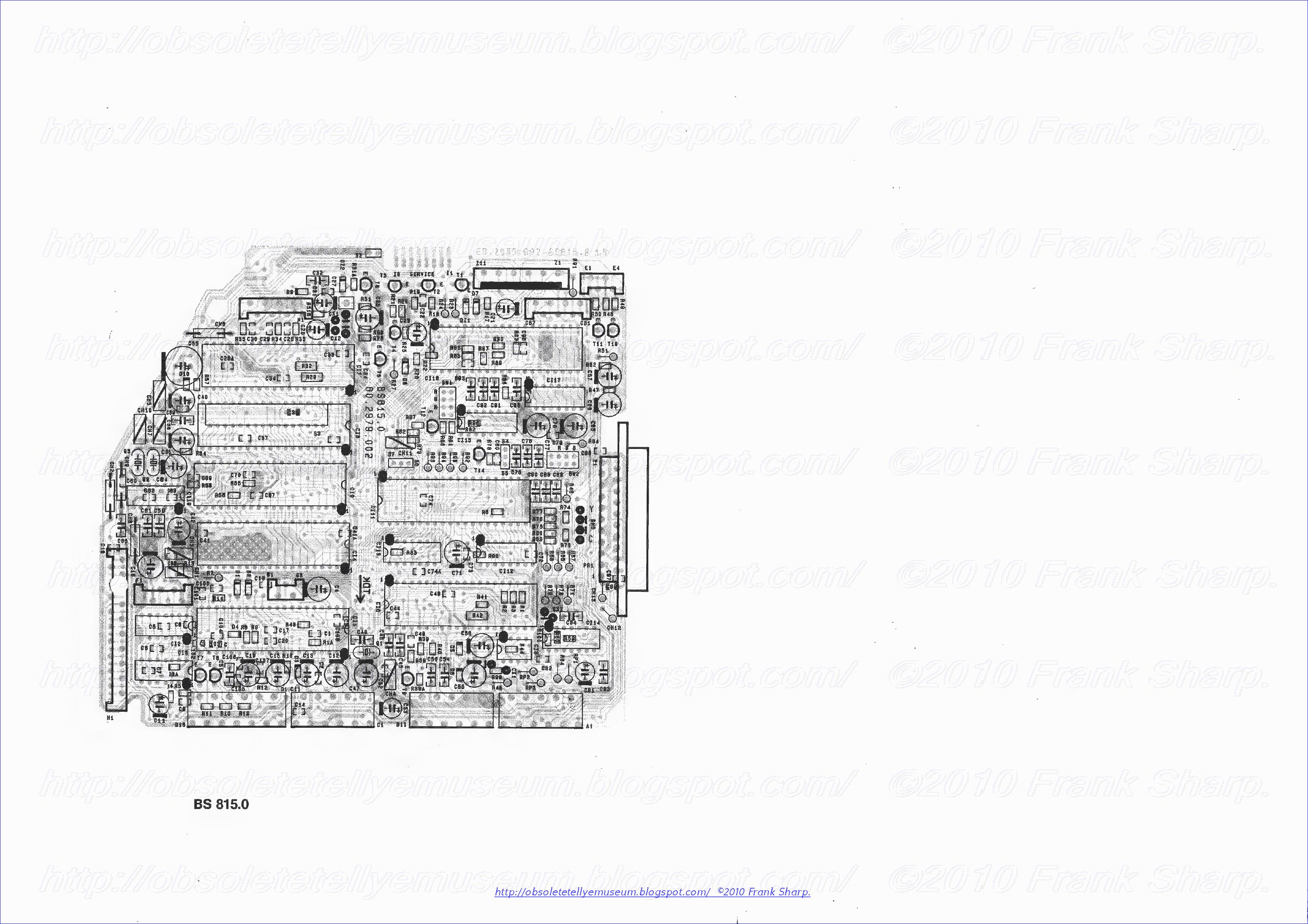
DIGITAL VIDEO BOARD BS 816.1 (BS815 BS816) VIEW


VCU 2133 A (ITT VCU2133 A) (Video Codec Decodec Unit)
DPU 2543 (ITT DPU2543) (Digital Deflection Processor Unit)
PVPU 2203 (ITT PVPU2203) (PAL and Video Processor Unit)
CCU-SECO-19 (CENTRAL CONTROL UNIT)
TPU 2732 (ITT TPU2732) (Teletext Processor Unit)
MCU 2600 (ITT MCU2600) (Main Clock Unit)
Contains DIGIT2000 Digital Video Processing ChipSet.
VCU 2133 A (ITT VCU2133 A) (Video Codec Decodec Unit)
DPU 2543 (ITT DPU2543) (Digital Deflection Processor Unit)
PVPU 2203 (ITT PVPU2203) (PAL and Video Processor Unit)
DTI 2222 (ITT DTI2222) (Digital Transient Improvement [Chroma])
TPU 2732 (ITT TPU2732) (Teletext Processor Unit)
MCU 2600 (ITT MCU2600) (Main Clock Unit)
ITT DIGIVISION CHIPSET FUNCTIONS.SELECO 25SS597P SIDERAL CHASSIS BS950
Set of 3 three integrated circuits for digital video signal processing in color-television receivers: ITT DIGIVISION.DIGITAL CRT TUBE Cathode RAY CURRENT CONTROL / Cut OFF / Drive and processing.
In
this IC set, the dark currents and the white levels of the three
electron guns, the leakage currents of the cathodes, and a
light-detector current are measured during four successive vertical
blanking intervals. The cathode leakage currents and the dark currents
are measured in the first half of the vertical blanking interval, and
the light-detector current and the white level currents are measured at
the end of this interval. From these measured data and alignment data
stored in a reprogrammable memory (ps), a microprocessor (mp) contained
together with the memory (ps) in an integrated circuit (ic2) derives
operating data for the picture tube (b) as well as further data. These
operating data are transferred over a wire of a chroma bus (cb), over
which chroma signals are transferred during the vertical sweep, into a
shift register (sr) of a further integrated circuit (ic3) at the
beginning of each vertical blanking interval, from where they are passed
on to the picture tube (b) in groups via digital-to-analog converters
and analog amplifiers. By the use of the chroma bus for a dual purpose,
and the successive measurements of the above-mentioned picture-tube
data, a saving of external terminals of the integrated circuits (ic1,
ic2, ic3) is achieved.
1. Set of three integrated circuits(ic1, ic2, ic3) for digital video-signal processing in color-television receivers,
wherein the first integrated circuit (ic1) contains an analog-to-digital converter (ad) followed by a first bus interface circuit (if1) for a serial data bus (sb), and a first multiplexer (mx1) following the first bus interface circuit (if1), the analog-to-digital converter (ad) being fed with measured data corresponding to the cathode currents of the picture tube (b) flowing at "black" (="dark current") and "white" (="white level") in each of the three electron guns, and with the signal of an ambient-light detector (ls) via a second multiplexer (mx) in the vertical blanking interval, and the first multiplexer (mx1) being fed with the processed digital chrominance signals (cs),
 wherein the second integrated circuit (ic2) contains a microprocessor
(mp), an electrically reprogrammable memory (ps), and a second
serial-data-bus interface circuit (if2) corresponding to the first bus
interface circuit (if1), the memory (ps) holding alignment data and
nominal dark-current/white-level data of the picture tube used (b) which
were entered by the manufacturer of the color-television receiver and,
together with the measured data, are used by the microprocessor (mp)
to generate video-signal-independent operating data for the picture
tube (b), and
wherein the second integrated circuit (ic2) contains a microprocessor
(mp), an electrically reprogrammable memory (ps), and a second
serial-data-bus interface circuit (if2) corresponding to the first bus
interface circuit (if1), the memory (ps) holding alignment data and
nominal dark-current/white-level data of the picture tube used (b) which
were entered by the manufacturer of the color-television receiver and,
together with the measured data, are used by the microprocessor (mp)
to generate video-signal-independent operating data for the picture
tube (b), and wherein the third integrated circuit (ic3) contains a demultiplexer (dx), an analog RGB matrix (m), and three analog amplifiers (vr, vg, vb) each designed to drive one of the electron guns via an external video output stage (ve), the dark current of the picture tube (b) being adjusted via the operating point of the respective analog amplifier, and the white level of the picture tube (b) being adjusted by adjusting the gain of the respective amplifier after digital-to-analog conversion, and with the demultiplexer (dx) connecte
d to the first multiplexer (mx1)of the first integrated circuit
(ic1) via a chroma bus (cb), 
Characterized by the Following Features:
The first multiplexer (mx1) consists of three electronic switches (s1, s2, s3),
the first of which (s1) has its input grounded through a first resistor (r1) and connected to the collectors of external transistors (tr, tg, tb) which are each associated with one of the electron guns and the base of each of which is driven by the associated video output stage, while the emitter is connected to the associated electron gun system, and the output of the first switch (s1) is connected to the input of the analog-to-digital converter (ad);
the second of which (s2) has its input connected to the light detector (ls), while its output is coupled with the input of the analog-to-digital converter (ad), and
the third of which (s3) has its input connected to the input of the first electronic switch (s1) via a second resistor (r2), and its output is grounded, the value of the second resistor (r2) being about one order of magnitude smaller than that of the first resistor (r1);
the three electronic switches (s1, s2, s3) have the following positions:
| ______________________________________ |
| s1 s2 s3 |
| ______________________________________ |
during vertical closed open closed sweep during vertical closed/open open/closed open/closed retrace: for leakage/light- det. current meas. for white level closed open closed measurement for dark current closed open open measurement |
| ______________________________________ |
to this end, the cathodes are connected at one end to a voltage for blacker than black (us), and at the other end to a voltage for black (ud) and then to a voltage for white (uw) in accordance with the following table:
| ______________________________________ |
| Measurement in the first at about the Vertical half of the end of the blanking vertical vertical interval blanking blanking Cathode No. interval interval red green blue |
| ______________________________________ |
1 Leakage cur- Light-detect- us us us rents of the or current cathodes 2 Dark current White level ud/uw us us red red 3 Dark current White level us ud/uw us green green 4 Dark current White level us us ud/uw blue blue |
| ______________________________________ |
the measured data are transferred from the analog-to-digital converter
(ad) to the microprocessor (mp) of the second integrated circuit (ic2)
via the two interface circuits (if1, if2) and the data bus (sb) at an
appropriate instant, and the video-signal-independent operating data for the picture tube (b), which are generated by the microprocessor (mp), are transferred from the second integrated circuit (ic2) via the two interface circuits (if1, if2) and a line (db) to the first multiplexer (mx1) of the first integrated circuit (ic1) at an appropriate instant, and from there over a wire of the chroma bus (cb) into a shift register (sr) of the third integrated circuit (ic3) shortly after the beginning of the next vertical blanking interval, the parallel outputs of which shift register (sr) are combined in groups each assigned to one type of operating value, and each of the groups is connected to one digital-to-analog converter (dh, ddr, ddg, ddd, dwr, dwg, dwb) which drives the RGB matrix (m) or the respective analog amplifier (vr, vg, vb).
. 2. An integrated-circuit set as claimed in claim 1, characterized in that the voltage for blacker than black (us) is applied to the cathodes of the picture tube (b) during the data transfer to the shift register (sr). 3. An integrated-circuit set as claimed in claim 2, characterized in that the microprocessor (mp) determines the appropriate instant for the measured-data transfer, and that, if a measurement has not yet been finished at that instant, the measured data of the corresponding earlier measurement are transferred. 4. An integrated-circuit set as claimed in claim 3, characterized in that the measurement performed in a vertical blanking interval is not enabled until the data of the preceding measurement have been transferred to the microprocessor (mp). 5. An integrated-circuit set as claimed in claim 2, characterized in that the measurement performed in a vertical blanking interval is not enabled until the data of the preceding measurement have been transferred to the microprocessor (mp). 6. An integrated-circuit set as claimed in claim 1, characterized in that the microprocessor (mp) determines the appropriate instant for the measured-data transfer, and that, if a measurement has not yet been finished at that instant, the measured data of the corresponding earlier measurement are transferred. 7. An integrated-circuit set as claimed in claim 6, characterized in that the measurement performed in a vertical blanking interval is not enabled until the data of the preceding measurement have been transferred to the microprocessor (mp). 8. An integrated-circuit set as claimed in claim 1, characterized in that the measurement performed in a vertical blanking interval is not enabled until the data of the preceding measurement have been transferred to the microprocessor (mp).
Description:
The
present invention relates to a set of three integrated circuits for
digital video signal processing in color-television receivers as is set
forth in the preamble of claim 1. An IC set of this kind is described
in a publication by INTERMETALL entitled "Eine neue
Dimension-VLSI-Digital-TV-System", Freiburg im Breisgau, September 1981,
on pages 6 to 11 (see also the corresponding English edition entitled
"A new dimension-VLSI Digital TV System", also dated September 1981).
 The
first integrated circuit, designated in the above-mentioned
publications by "MAA 2200" and called "Video Processor Unit" (VPU),
includes an analog-to-digital converter followed by a first
serial-data-bus interface circuit which, in turn, is followed by a first
multiplexer. During the vertical blanking interval, the
analog-to-digital converter is fed, via a second multiplexer, with
measured data corresponding to the cathode currents of the picture tube
flowing at "black" (="dark current") and "white" ("white level") in
each of the three electron guns, and with the signal of an
ambient-light detector. The processed digital chrominance signals are
applied to the first multiplexer.
The
first integrated circuit, designated in the above-mentioned
publications by "MAA 2200" and called "Video Processor Unit" (VPU),
includes an analog-to-digital converter followed by a first
serial-data-bus interface circuit which, in turn, is followed by a first
multiplexer. During the vertical blanking interval, the
analog-to-digital converter is fed, via a second multiplexer, with
measured data corresponding to the cathode currents of the picture tube
flowing at "black" (="dark current") and "white" ("white level") in
each of the three electron guns, and with the signal of an
ambient-light detector. The processed digital chrominance signals are
applied to the first multiplexer.
The second integrated circuit, designated by "MAA 2000" and called "central control unit" (CCU) in the above publications, contains a microprocessor, an electrically reprogrammable memory, and a second serial-data-bus interface circuit. The memory holds alignment data and nominal dark-current/white-level data entered by the manufacturer of the color-television receiver. From these data and the measured data, the microprocessor derives video-signal-independent operating data for the picture tube.
The third integrated circuit, designated by "MAA 21 00"
and called "video-codec unit" (VCU) in the above publications,
includes a demultiplexer, an analog RGB matrix, and three analog
amplifiers each designed to drive one of the electron guns via an
external video output stage. After digital-to-analog conversion, the
dark current of the picture tube is adjusted via the operating point of
the respective analog amplifier, and the white level of the picture
tube is adjusted by adjusting the gain of the respective analog
amplifier. The demultiplexer is connected to the first multiplexer of
the first integrated circuit via a chroma bus.
00"
and called "video-codec unit" (VCU) in the above publications,
includes a demultiplexer, an analog RGB matrix, and three analog
amplifiers each designed to drive one of the electron guns via an
external video output stage. After digital-to-analog conversion, the
dark current of the picture tube is adjusted via the operating point of
the respective analog amplifier, and the white level of the picture
tube is adjusted by adjusting the gain of the respective analog
amplifier. The demultiplexer is connected to the first multiplexer of
the first integrated circuit via a chroma bus.
As to the prior art concerning such digital color-television receiver systems, reference is also made to the journal "Elektronik", Aug. 14, 1981 (No. 16), pages 27 to 35, and the journal "Electronics", Aug. 11, 1981, pages 97 to 103.
During the further development of the prior art system following the above-mentioned publication dates, the developers were faced with the problem of how to accomplish the dark-current/white-level control of the picture tube within the existing system, particularly with respect to measured-data acquisition and transfer and to the transfer of the operating data to the picture tube.
Another requirement imposed during the further development of the prior art system was that the leakage currents of the electron guns of the picture tube be measured and processed within the existing system. The solution of these problems is to take into account the requirement that the number of external terminals of the individual integrated circuits be kept to a minimum.
The object of the invention as claimed is to solve the problems pointed out. The essential principles of the solution, which directly give the advantages of the invention, are, on the one hand, the division of the measurement to four successive vertical blanking intervals and, on the other hand, the utilization of one wire of the chroma bus at the beginning of the next vertical blanking interval as well as the measurement of the ambient light by means of the light detector and the measurement of the leakage currents during a single vertical blanking interval.
The invention will now be explained in more detail with reference to the accompanying drawing, which is a block diagram of one embodiment of the IC set in accordance with the invention. It shows the first, second, and third integrated circuits ic1, ic2, and ic3, which are drawn as rectangles bordered by heavy lines. The first integrated circuit ic1 includes the analog-to-digital converter ad, which converts the measured dark-current, white-level, ambient-light, and leakage-current data into digital signals, which are fed to the first bus interface circuit if1. The latter is connected via the line db to the first multiplexer mx1, which interleaves data from the first bus interface circuit if1 with digital chrominance signals cs produced in the first integrated circuit ic1, and places the interleaved signals on the chroma bus cb. The generation of the digital chrominance signals cs is outside the scope of the present invention and is disclosed in the references cited above.
The first integrated circuit ic1 further includes the second multiplexer mx2, which consists of the three electronic switches s1, s2, s3, and represents a subcircuit which is essential for the invention. The input of the first switch s1 is grounded through the first resistor r1, and connected to the collectors of the external transistors tr, tg, tb, each of which is associated with one of the electron guns. Via the base-emitter paths of these transistors, the cathodes of the three electron guns are driven by the video output stages ve. The final letters r, g, and b in the reference characters tr, tg, and tb and in the reference characters explained later indicate the assignment to the electron gun for RED (r), GREEN (g), and BLUE (b), respectively. The output of the first switch s1 is connected to the input of the analog-to-digital converter ad.
The input of the second switch s2 is connected to the light detector ls, which has its other terminal connected to a fixed voltage u and combines with the grounded resistor r3 to form a voltage divider. The input of the second switch s2 is thus connected to the tap of this voltage divider, while the output of this switch, too, is coupled to the input of the analog-to-digital converter ad.
The input of the third switch s3 is connected to the input of the first switch s1 via the second resistor r2, while the output of the third switch s3 is grounded. The value of the resistor r1 is about one order of magnitude greater than that of the resistor r2.
For
the whole duration of the picture shown on the screen of the picture
tube b, and throughout the vertical sweep, the first switch s1 and the
third switch s3 are closed, and the second switch s2 is open. During the
vertical retrace interval, for the white-level measurement, the
switches s1, s3 are closed, and the switch s2 is open; for the
dark-current measurement and the leakage-current measurement, the switch
s1 is closed, and the switches s2, s3 are open, and for the
light-detector-current measurement, the switches s2, s3 are closed, and
the switch s1 is open.
The measurements of the dark current and the white level of each electron gun and the measurements of the light-detector current and the leakage currents are made in four successive vertical blanking intervals. One end of the respective cathode is connected to a voltage us for blacker-than-black, and the other end is connected to a voltage ud for black and then to a voltage uw for white, in accordance with the following table:
The voltage ud for black is, as usual, a voltage
which just causes no brightness on the screen of the picture tube b,
i.e., a voltage just below the dark threshold of the picture tube. The
voltage us for blacker-than-block is then a cathode vol tage lying
further in the black direction than the voltage for black. The voltage
for white is the voltage for the screen brightness to be measured; the
brightness of the screen is generally below the maximum permissible
value.
tage lying
further in the black direction than the voltage for black. The voltage
for white is the voltage for the screen brightness to be measured; the
brightness of the screen is generally below the maximum permissible
value.
Thus, two measurements are made during each vertical blanking interval, namely one in the first half, preferably at one-third of the pulse duration of the vertical blanking interval, and the other at about the end of the first half. During the four successive vertical blanking intervals, the first measurement determines the leakage currents of the cathodes and the dark currents for red, green, and blue. The second measurements determine the light-detector current and the white levels for red, green, and blue. During the measurement of the cathode leakage currents and the light-detector current, all three cathodes are at the voltage us. During the measurements of the dark current and the white level of the respective cathode, the latter is connected to the respective dark-current cathode voltage ud and white-level cathode voltage uw, respectively, while the cathodes of the two other electron guns, which are not being measured, are at the voltage us.
The second integrated circuit circuit ic2 contains the microprocessor mp, the electrically reprogrammable memory ps, and the second bus interface circuit if2, which is associated with the serial data bus sb in this integrated circuit and also connects the microprocessor mp and the memory ps with one another and with itself. The memory ps holds alignment data and nominal dark-current/white-value data of the picture tube used, which were entered by the manufacturer. From this alignment and nominal data and from the measured data obtained via the second multiplexer mx2 and the analog-to-digital converter ad of the first integrated circuit ic1, the microprocessor mp derives video-signal-independent operating data for the picture tube.
The derivation of these operating data is also outside the scope of the invention; it should only be mentioned that with respect to the operating data of the picture tube, the microprocessor performs a control function in accordance with a predetermined control characteristic.
The third integrated circuit ic3 includes the demultiplexer dx, which is connected to the first multiplexer mx1 of the first integrated circuit ic1 via the chroma bus cb and separates the chrominance signals cs and the operating data of the picture tube from the interleaved signals
transferred over the chroma bus. While the transfer of measured data
from the analog-to-digital converter ad to the microprocessor mp of the
second integrated circuit ic2 takes place via the two interface
circuits if1, if2 and the data bus sb at an appropriate instant, the
video-signal-independent operating data for the picture tube b, which
are derived by the microprocessor mp, are transferred from the second
integrated circuit ic2 via the two interface circuits if1, if2 and the
line db to the first multiplexer mx1 at an appropriate instant, and
from the first multiplexer mx1 over a wire of the chroma bus cb into
the shift register sr of the third integrated circuit ic3 shortly after
the beginning of the next vertical blanking interval. To accomplish
this, the first interface circuit if1 also includes a shift register
from which the operating data are read serially.
During this data transfer into the shift register sr, the cathodes of the picture tube b are preferably at the voltage us in order that this data transfer does not become visible on the screen.
The appropriate instant for the transfer of measured data to the microprocessor mp is determined by the latter itself, i.e., depending on the program being executed in the microprocessor, and on the time needed therefor, the measured data are called for from the interface circuits not at the time of measurement but at a selectable instant within the working program of the microprocessor mp. If the measurement currently being performed should not yet be finished at the instant at which the measured data are called for, in a preferred embodiment of the invention, the stored data of the previous measurement will be transferred to the microprocessor mp.
As mentioned previously, the operating data for the picture tube b are transferred into the shift register sr at the beginning of a vertical blanking interval. The parallel outputs of this shift register are combined in groups each assigned to one operating value, and each group has one of the digital-to-analog converters dh, ddr, ddg, ddb, dwr, dwg, dwb associated with it. In the figure, the division of the shift register into groups is indicated by broken lines. The shift register sr performs a serial-to-parallel conversion in the usual manner, and the operating data are entered by the demultiplexer dx into the shift register in serial form and are then available at the parallel outputs of the shift register.
The digital-to-analog converter dh provides the analog brightness control signal, which is applied to the RGB matrix m in the integrated circuit ic3. Also applied to the RGB matrix m are the analog color-difference signals r-y, b-y and the luminance signal y. The formation of these signals is outside the scope of the invention and is known per se from the publications cited at the beginning.
The three analog-to-digital converters ddr, ddg, ddb provide the dark-current-adjusting signals for the three cathodes, which are currents and are applied to the inverting inputs--of the analog amplifiers vr, vg, vb. Also connected to these inputs is a resistor network which is adjustable in steps in response to the digital white-level-adjusting signals at the respective group outputs of the shift register sr. The resistors serve as digital-to-analog converters dwr, dwg, dwb and establish the connection between the inverting inputs--and the outputs of the analog amplifiers vr, vg, vb.
In an arrangement according to the invention which has proved good in practice, each of the three dark-current-adjusting signals is a seven-digit signal, and each of the
three white-level-adjusting signals and the brightness control signal
are five-digit signals. The voltages us and ud/uw of the three cathodes
are assigned a three-digit identification signal in accordance with
the above table, which signal is also fed into the shift register sr in
the implemented circuit. Finally, a three-digit contrast control
signal is provided in the implemented circuit for the Teletext mode of
the color-television receiver. These nine data blocks are transferred
in the implemented circuit from the demultiplexer dx to the shift
register sr in the following order, with the least significant bit
transmitted first, and with the specified number of blanks:
identification signal, white-level signal blue, three blanks,
white-level signal green, three blanks, white-level signal red, one
blank, dark-current signal blue, one blank, dark-current signal green,
one blank, dark-current signal red, contrast signal Teletext, and
brightness control signal. These are seven eight-digit data blocks
which are assigned to 56 pulses of a 4.4-MHz clock frequency, which is
the frequency of the shift clock signal of the shift register sr.
the
three white-level-adjusting signals and the brightness control signal
are five-digit signals. The voltages us and ud/uw of the three cathodes
are assigned a three-digit identification signal in accordance with
the above table, which signal is also fed into the shift register sr in
the implemented circuit. Finally, a three-digit contrast control
signal is provided in the implemented circuit for the Teletext mode of
the color-television receiver. These nine data blocks are transferred
in the implemented circuit from the demultiplexer dx to the shift
register sr in the following order, with the least significant bit
transmitted first, and with the specified number of blanks:
identification signal, white-level signal blue, three blanks,
white-level signal green, three blanks, white-level signal red, one
blank, dark-current signal blue, one blank, dark-current signal green,
one blank, dark-current signal red, contrast signal Teletext, and
brightness control signal. These are seven eight-digit data blocks
which are assigned to 56 pulses of a 4.4-MHz clock frequency, which is
the frequency of the shift clock signal of the shift register sr.
It should be noted that the data sequence just described does not correspond to the order of the groups of the shift register sr in the figure. The order in the figure was chosen only for the sake of clarity.
The outputs of the three analog amplifiers vr, vg, vb are coupled to the inputs of the video output stage ve, whose outputs, as explained previously, are connected to the bases of the transistors pr, tg, td, so that the cathodes of the picture tube b are driven via the base-emitter paths of these transistors.
In another preferred embodiment of the invention, the measurement performed during a vertical blanking interval is not enabled until the data of the previous measurement has been transferred into the microprocessor mp. In this manner, no measurement will be left out.
It is also possible to omit the digital-to-analog converter dh if the analog RGB matrix m is replaced with a digital one.
One advantage of the invention is that the use of the chroma bus for the transfer of operating data facilitates the implementation of the third integrated circuit ic3 using bipolar technology, because an additional bus interface circuit, which could be used there, would occupy too much chip area.
The
first integrated circuit, designated in the above-mentioned
publications by "MAA 2200" and called "Video Processor Unit" (VPU),
includes an analog-to-digital converter followed by a first
serial-data-bus interface circuit which, in turn, is followed by a first
multiplexer. During the vertical blanking interval, the
analog-to-digital converter is fed, via a second multiplexer, with
measured data corresponding to the cathode currents of the picture tube
flowing at "black" (="dark current") and "white" ("white level") in
each of the three electron guns, and with the signal of an
ambient-light detector. The processed digital chrominance signals are
applied to the first multiplexer. The second integrated circuit, designated by "MAA 2000" and called "central control unit" (CCU) in the above publications, contains a microprocessor, an electrically reprogrammable memory, and a second serial-data-bus interface circuit. The memory holds alignment data and nominal dark-current/white-level data entered by the manufacturer of the color-television receiver. From these data and the measured data, the microprocessor derives video-signal-independent operating data for the picture tube.
The third integrated circuit, designated by "MAA 21
00"
and called "video-codec unit" (VCU) in the above publications,
includes a demultiplexer, an analog RGB matrix, and three analog
amplifiers each designed to drive one of the electron guns via an
external video output stage. After digital-to-analog conversion, the
dark current of the picture tube is adjusted via the operating point of
the respective analog amplifier, and the white level of the picture
tube is adjusted by adjusting the gain of the respective analog
amplifier. The demultiplexer is connected to the first multiplexer of
the first integrated circuit via a chroma bus. As to the prior art concerning such digital color-television receiver systems, reference is also made to the journal "Elektronik", Aug. 14, 1981 (No. 16), pages 27 to 35, and the journal "Electronics", Aug. 11, 1981, pages 97 to 103.
During the further development of the prior art system following the above-mentioned publication dates, the developers were faced with the problem of how to accomplish the dark-current/white-level control of the picture tube within the existing system, particularly with respect to measured-data acquisition and transfer and to the transfer of the operating data to the picture tube.
Another requirement imposed during the further development of the prior art system was that the leakage currents of the electron guns of the picture tube be measured and processed within the existing system. The solution of these problems is to take into account the requirement that the number of external terminals of the individual integrated circuits be kept to a minimum.
The object of the invention as claimed is to solve the problems pointed out. The essential principles of the solution, which directly give the advantages of the invention, are, on the one hand, the division of the measurement to four successive vertical blanking intervals and, on the other hand, the utilization of one wire of the chroma bus at the beginning of the next vertical blanking interval as well as the measurement of the ambient light by means of the light detector and the measurement of the leakage currents during a single vertical blanking interval.
The invention will now be explained in more detail with reference to the accompanying drawing, which is a block diagram of one embodiment of the IC set in accordance with the invention. It shows the first, second, and third integrated circuits ic1, ic2, and ic3, which are drawn as rectangles bordered by heavy lines. The first integrated circuit ic1 includes the analog-to-digital converter ad, which converts the measured dark-current, white-level, ambient-light, and leakage-current data into digital signals, which are fed to the first bus interface circuit if1. The latter is connected via the line db to the first multiplexer mx1, which interleaves data from the first bus interface circuit if1 with digital chrominance signals cs produced in the first integrated circuit ic1, and places the interleaved signals on the chroma bus cb. The generation of the digital chrominance signals cs is outside the scope of the present invention and is disclosed in the references cited above.
The first integrated circuit ic1 further includes the second multiplexer mx2, which consists of the three electronic switches s1, s2, s3, and represents a subcircuit which is essential for the invention. The input of the first switch s1 is grounded through the first resistor r1, and connected to the collectors of the external transistors tr, tg, tb, each of which is associated with one of the electron guns. Via the base-emitter paths of these transistors, the cathodes of the three electron guns are driven by the video output stages ve. The final letters r, g, and b in the reference characters tr, tg, and tb and in the reference characters explained later indicate the assignment to the electron gun for RED (r), GREEN (g), and BLUE (b), respectively. The output of the first switch s1 is connected to the input of the analog-to-digital converter ad.
The input of the second switch s2 is connected to the light detector ls, which has its other terminal connected to a fixed voltage u and combines with the grounded resistor r3 to form a voltage divider. The input of the second switch s2 is thus connected to the tap of this voltage divider, while the output of this switch, too, is coupled to the input of the analog-to-digital converter ad.
The input of the third switch s3 is connected to the input of the first switch s1 via the second resistor r2, while the output of the third switch s3 is grounded. The value of the resistor r1 is about one order of magnitude greater than that of the resistor r2.
For
the whole duration of the picture shown on the screen of the picture
tube b, and throughout the vertical sweep, the first switch s1 and the
third switch s3 are closed, and the second switch s2 is open. During the
vertical retrace interval, for the white-level measurement, the
switches s1, s3 are closed, and the switch s2 is open; for the
dark-current measurement and the leakage-current measurement, the switch
s1 is closed, and the switches s2, s3 are open, and for the
light-detector-current measurement, the switches s2, s3 are closed, and
the switch s1 is open. The measurements of the dark current and the white level of each electron gun and the measurements of the light-detector current and the leakage currents are made in four successive vertical blanking intervals. One end of the respective cathode is connected to a voltage us for blacker-than-black, and the other end is connected to a voltage ud for black and then to a voltage uw for white, in accordance with the following table:
| ______________________________________ |
| Measurement in the first at about the Vertical half of the end of the blanking vertical vertical interval blanking blanking Cathode No. interval interval red green blue |
| ______________________________________ |
1 Leakage cur- Light-detect- us us us rents of the or current cathodes 2 Dark current White level ud/uw us us red red 3 Dark current White level us ud/uw us green green 4 Dark current White level us us ud/uw blue blue |
| ______________________________________ |
tage lying
further in the black direction than the voltage for black. The voltage
for white is the voltage for the screen brightness to be measured; the
brightness of the screen is generally below the maximum permissible
value. 
Thus, two measurements are made during each vertical blanking interval, namely one in the first half, preferably at one-third of the pulse duration of the vertical blanking interval, and the other at about the end of the first half. During the four successive vertical blanking intervals, the first measurement determines the leakage currents of the cathodes and the dark currents for red, green, and blue. The second measurements determine the light-detector current and the white levels for red, green, and blue. During the measurement of the cathode leakage currents and the light-detector current, all three cathodes are at the voltage us. During the measurements of the dark current and the white level of the respective cathode, the latter is connected to the respective dark-current cathode voltage ud and white-level cathode voltage uw, respectively, while the cathodes of the two other electron guns, which are not being measured, are at the voltage us.
The second integrated circuit circuit ic2 contains the microprocessor mp, the electrically reprogrammable memory ps, and the second bus interface circuit if2, which is associated with the serial data bus sb in this integrated circuit and also connects the microprocessor mp and the memory ps with one another and with itself. The memory ps holds alignment data and nominal dark-current/white-value data of the picture tube used, which were entered by the manufacturer. From this alignment and nominal data and from the measured data obtained via the second multiplexer mx2 and the analog-to-digital converter ad of the first integrated circuit ic1, the microprocessor mp derives video-signal-independent operating data for the picture tube.
The derivation of these operating data is also outside the scope of the invention; it should only be mentioned that with respect to the operating data of the picture tube, the microprocessor performs a control function in accordance with a predetermined control characteristic.
The third integrated circuit ic3 includes the demultiplexer dx, which is connected to the first multiplexer mx1 of the first integrated circuit ic1 via the chroma bus cb and separates the chrominance signals cs and the operating data of the picture tube from the interleaved sig
nals
transferred over the chroma bus. While the transfer of measured data
from the analog-to-digital converter ad to the microprocessor mp of the
second integrated circuit ic2 takes place via the two interface
circuits if1, if2 and the data bus sb at an appropriate instant, the
video-signal-independent operating data for the picture tube b, which
are derived by the microprocessor mp, are transferred from the second
integrated circuit ic2 via the two interface circuits if1, if2 and the
line db to the first multiplexer mx1 at an appropriate instant, and
from the first multiplexer mx1 over a wire of the chroma bus cb into
the shift register sr of the third integrated circuit ic3 shortly after
the beginning of the next vertical blanking interval. To accomplish
this, the first interface circuit if1 also includes a shift register
from which the operating data are read serially. During this data transfer into the shift register sr, the cathodes of the picture tube b are preferably at the voltage us in order that this data transfer does not become visible on the screen.
The appropriate instant for the transfer of measured data to the microprocessor mp is determined by the latter itself, i.e., depending on the program being executed in the microprocessor, and on the time needed therefor, the measured data are called for from the interface circuits not at the time of measurement but at a selectable instant within the working program of the microprocessor mp. If the measurement currently being performed should not yet be finished at the instant at which the measured data are called for, in a preferred embodiment of the invention, the stored data of the previous measurement will be transferred to the microprocessor mp.
As mentioned previously, the operating data for the picture tube b are transferred into the shift register sr at the beginning of a vertical blanking interval. The parallel outputs of this shift register are combined in groups each assigned to one operating value, and each group has one of the digital-to-analog converters dh, ddr, ddg, ddb, dwr, dwg, dwb associated with it. In the figure, the division of the shift register into groups is indicated by broken lines. The shift register sr performs a serial-to-parallel conversion in the usual manner, and the operating data are entered by the demultiplexer dx into the shift register in serial form and are then available at the parallel outputs of the shift register.
The digital-to-analog converter dh provides the analog brightness control signal, which is applied to the RGB matrix m in the integrated circuit ic3. Also applied to the RGB matrix m are the analog color-difference signals r-y, b-y and the luminance signal y. The formation of these signals is outside the scope of the invention and is known per se from the publications cited at the beginning.
The three analog-to-digital converters ddr, ddg, ddb provide the dark-current-adjusting signals for the three cathodes, which are currents and are applied to the inverting inputs--of the analog amplifiers vr, vg, vb. Also connected to these inputs is a resistor network which is adjustable in steps in response to the digital white-level-adjusting signals at the respective group outputs of the shift register sr. The resistors serve as digital-to-analog converters dwr, dwg, dwb and establish the connection between the inverting inputs--and the outputs of the analog amplifiers vr, vg, vb.
In an arrangement according to the invention which has proved good in practice, each of the three dark-current-adjusting signals is a seven-digit signal, and each of
the
three white-level-adjusting signals and the brightness control signal
are five-digit signals. The voltages us and ud/uw of the three cathodes
are assigned a three-digit identification signal in accordance with
the above table, which signal is also fed into the shift register sr in
the implemented circuit. Finally, a three-digit contrast control
signal is provided in the implemented circuit for the Teletext mode of
the color-television receiver. These nine data blocks are transferred
in the implemented circuit from the demultiplexer dx to the shift
register sr in the following order, with the least significant bit
transmitted first, and with the specified number of blanks:
identification signal, white-level signal blue, three blanks,
white-level signal green, three blanks, white-level signal red, one
blank, dark-current signal blue, one blank, dark-current signal green,
one blank, dark-current signal red, contrast signal Teletext, and
brightness control signal. These are seven eight-digit data blocks
which are assigned to 56 pulses of a 4.4-MHz clock frequency, which is
the frequency of the shift clock signal of the shift register sr. It should be noted that the data sequence just described does not correspond to the order of the groups of the shift register sr in the figure. The order in the figure was chosen only for the sake of clarity.
The outputs of the three analog amplifiers vr, vg, vb are coupled to the inputs of the video output stage ve, whose outputs, as explained previously, are connected to the bases of the transistors pr, tg, td, so that the cathodes of the picture tube b are driven via the base-emitter paths of these transistors.
In another preferred embodiment of the invention, the measurement performed during a vertical blanking interval is not enabled until the data of the previous measurement has been transferred into the microprocessor mp. In this manner, no measurement will be left out.
It is also possible to omit the digital-to-analog converter dh if the analog RGB matrix m is replaced with a digital one.
One advantage of the invention is that the use of the chroma bus for the transfer of operating data facilitates the implementation of the third integrated circuit ic3 using bipolar technology, because an additional bus interface circuit, which could be used there, would occupy too much chip area.
SELECO 25SS597P SIDERAL CHASSIS BS950 Color-television receiver having integrated circuit for the luminance signal and the chrominance signals:
VIDEO CODEC UNIT (VCU).
 The
invention permits an n bit resolution to be achieved with an n-1 bit
converter. In a color television receiver the analog-to-digital
converter is a parallel analog-to-digital converter with p=2r
-1 differential amplifiers as comparators, where r is the number of
binary digits of the output signal of the analog-to-digital converter
minus one. The composite color signal is then applied as the input
signal to the noninverting (or inverting) inputs of all p differential
amplifiers and the inverting (noninverting) inputs of the differential
amplifiers being connected successively to the taps of a resistive
voltage divider which contains equal-value resistors and is fed with a
reference voltage (Ur).
The
invention permits an n bit resolution to be achieved with an n-1 bit
converter. In a color television receiver the analog-to-digital
converter is a parallel analog-to-digital converter with p=2r
-1 differential amplifiers as comparators, where r is the number of
binary digits of the output signal of the analog-to-digital converter
minus one. The composite color signal is then applied as the input
signal to the noninverting (or inverting) inputs of all p differential
amplifiers and the inverting (noninverting) inputs of the differential
amplifiers being connected successively to the taps of a resistive
voltage divider which contains equal-value resistors and is fed with a
reference voltage (Ur).For the duration of every second line, either the reference voltage or the input signal is shifted by ΔU=0.5 Ur/2r.
1. A color-television receiver comprising at least one integrated circuit for separating and conditioning the luminance signal and the chrominance signals from the composite color signal, said integrated circuit containing:
a chrominance-subcarrier oscillator,
a chrominance-subcarrier band-pass filter,
a synchronous demodulator,
a PAL switch,
a color matrix, and, if necessary,
an R--G--B matrix, and being characterized by the following subcircuits for conditioning digital signals:
the chrominance-subcarrier oscillator is a squarewave clock generator providing four clock signals the first of which has four times the chrominance-subcarrier frequency and the second to fourth of which have the chrominance-subcarrier frequency, with the first and second clock signals having a pulse duty factor of 0.5, and the third and fourth clock signals each consisting of two consecutive, T/2-long pulses separated by T/2 within each 4T-long period (T=period of the first clock signal);
an analog-to-digital converter clocked by the first clock signal,
whose analog input is presented with the composite color signal, and
which forms as its output signal a parallel binary word from the
amplitude of the composite color signal (F) at the instants the
respective amplitudes of the undemodulated chrominance signal are equal
to the amplitudes of the respective color-difference signal; a first binary arithmetic stage which multiplies the output signal of the analog-to-digital converter by a binary overall-contrast control signal;
a two-stage delay line which delays the output signal of the first binary arithmetic stage by T/2;
a second binary arithmetic stage which forms the arithmetic mean of the delayed and undelayed output signals of the first binary arithmetic stage;
a third binary arithmetic stage which subtracts the output signal of the second binary arithmetic stage from the output signal of the first delay stage;
a buffer-memory arrangement which temporarily stores the output signal of the third binary arithmetic stage, and whose enable input is fed with the third clock signal;
a shift-register arrangement consisting of n parallel shift registers (n=number of bits at the output of the third binary arithmetic stage) each of which provides a delay of one line period and whose serial inputs are connected to the parallel outputs of the buffer-memory arrangement, while their clock inputs are fed with the fourth clock signal;
a fourth
binary arithmetic stage which
forms the arithmetic mean of the input and output signals of the
shift-register arrangement; a fifth binary arithmetic stage which subtracts the input signal of the shift-register arrangement from the output signal of this arrangement and then divides the difference by two;
a sixth binary arithmetic stage which, controlled by the PAL switch, either leaves the output signal of the fifth binary arithmetic stage unchanged or forms its absolute value;
a seventh binary arithmetic stage which forms the green color-difference signal from the output signals of the fourth and sixth binary arithmetic stages;
the outputs of the second, fourth, sixth and seventh binary arithmetic stages are connected to the binary R-G-B matrix each of whose outputs is coupled to one of three digital-to-analog converters for deriving the analog signals for controlling the R-G-B values of the picture tube, or
the outputs of the second, fourth, sixth and seventh binary arithmetic stages are each connected to one of four digital-to-analog converters for deriving the analog signals for controlling the color-difference value of the picture tube;
the improvement wherein
the analog-to-digital converter is a parallel analog-to-digital converter with p=2r -1 differential amplifiers as comparators, where r is the number of binary digits of the output signal of the analog-to-digital converter minus one, the composite color signal being applied as the input signal to one of the noninverting or inverting inputs of all p differential amplifiers and the other of the inverting or noninverting inputs of the differential amplifiers being connected successively to the taps of a resistive voltage divider which contains equal-value resistors and is fed with a reference voltage (Ur), and
for the duration of every second line, either the reference voltage (Ur) or the input signal (F) is shifted by ΔU=0.5 Ur/2r.
Description:
FIELD OF THE INVENTION
 Color-television
receivers comprising at least one integrated circuit for separating
and conditioning the luminance signal and the chrominance signals from
the composite color signal are known in the art. The particular
color-television receiver of such a known type comprises at least one
integrated circuit for separating and conditioning the luminance signal
and the chrominance signals from the composite color signal. This
integrated circuit contains a chrominance-subcarrier oscillator, a
chrominance-subcarrier band-pass filter, a synchronous demodulator, a
PAL switch, a color matrix, and, if necessary, an R-G-B matrix.
Additionally, such a color-television receiver contains the following
subcircuits for conditioning digital signals; (1) the
chrominance-subcarrier oscillator is a square-wave clock generator
providing four clock signals the first of which has four times the
chrominance-subcarrier frequency and the second to fourth of which have
the chrominance-subcarrier frequency, with the first and second clock
signals having a pulse duty factor of 0.5, and the third and fourth
clock signals each consisting of two consecutive, T/2-long pulses
separated by T/2 within each 4T-long period (T=period of the first clock
signal); (2) an analog-to-digital converter clocked by the first clock
signal, whose analog input is presented with the composite color
signal, and which forms as its output signal a parallel binary word
from the amplitude of the composite color signal (F) at the instants
the respective amplitudes of the undemodulated chrominance signal are
equal to the amplitudes of the respective color-difference signal; (3) a
first binary arithmetic stage which multiplies the output signal of
the analog-to-digital converter by a binary overall-contrast control
signal; (4) a two stage delay line which delays the output signal of
the first binary arithmetic stage by T/2; (5) a second binary
arithmetic stage which forms the arithmetic means of the delayed and
undelayed output signals of the first binary arithmetic stage; (6) a
third binary arithmetic stage, which subtracts the output signal of the
second binary arithmetic stage from the output signal of the first
delay stage; (7) a buffer-memory arrangement which temporarily stores
the output signal of the third binary arithmetic stage, and whose
enable input is fed with the third clock signal; (8) a shift-register
arrangement consisting of n parallel shift registers (n=number of bits
at the output of the third binary arithmetic stage) each of which
provides a delay of one line period and whose serial inputs are
connected to the parallel outputs of the buffer-memory arrangement,
while their clock inputs are fed with the fourth clock signal; (9) a
fourth binary arithmetic stage which forms the arithmetic mean of the
input and output signals of the shift-register arrangement; (10) a
fifth binary arithmetic stage which subtracts the input signal of the
shift-register arrangement from the output signal of this arrangement
and then divides the difference by two; (11) a sixth binary arithmetic
stage which, controlled by the PAL switch, either leaves the output
signal of the fifth binary arithmetic stage unchanged or forms its
absolute value; (12) a seventh binary arithmetic stage which forms the
green color-difference signal from the output signals of the fourth and
sixth binary arithmetic stages; (13) the outputs of the second,
fourth, sixth and seventh binary arithmetic stages are connected to the
binary R-G-B matrix each of whose outputs is coupled to one of three
digital-to-analog converters for deriving the analog signals for
controlling the R-G-B values of the picture tube, or (14) the outputs
of the second, fourth, sixth and seventh binary arithmetic stages are
each connected to one of four digital-to-analog converters for deriving
the analog signals for controlling the color-difference values of the
picture tube. An essential feature of such a receiver is the use of an
analog-to-digital converter whose analog input is presented with the
composite color signal and which is clocked by a clock signal at four
times the chrominance-subcarrier frequency, so that a parallel binary
word is obtained from the amplitudes of the composite color signal at
the instants the respective amplitudes of the undemodulated chrominance
signal are equal to the amplitudes of the respective color-difference
signal.
Color-television
receivers comprising at least one integrated circuit for separating
and conditioning the luminance signal and the chrominance signals from
the composite color signal are known in the art. The particular
color-television receiver of such a known type comprises at least one
integrated circuit for separating and conditioning the luminance signal
and the chrominance signals from the composite color signal. This
integrated circuit contains a chrominance-subcarrier oscillator, a
chrominance-subcarrier band-pass filter, a synchronous demodulator, a
PAL switch, a color matrix, and, if necessary, an R-G-B matrix.
Additionally, such a color-television receiver contains the following
subcircuits for conditioning digital signals; (1) the
chrominance-subcarrier oscillator is a square-wave clock generator
providing four clock signals the first of which has four times the
chrominance-subcarrier frequency and the second to fourth of which have
the chrominance-subcarrier frequency, with the first and second clock
signals having a pulse duty factor of 0.5, and the third and fourth
clock signals each consisting of two consecutive, T/2-long pulses
separated by T/2 within each 4T-long period (T=period of the first clock
signal); (2) an analog-to-digital converter clocked by the first clock
signal, whose analog input is presented with the composite color
signal, and which forms as its output signal a parallel binary word
from the amplitude of the composite color signal (F) at the instants
the respective amplitudes of the undemodulated chrominance signal are
equal to the amplitudes of the respective color-difference signal; (3) a
first binary arithmetic stage which multiplies the output signal of
the analog-to-digital converter by a binary overall-contrast control
signal; (4) a two stage delay line which delays the output signal of
the first binary arithmetic stage by T/2; (5) a second binary
arithmetic stage which forms the arithmetic means of the delayed and
undelayed output signals of the first binary arithmetic stage; (6) a
third binary arithmetic stage, which subtracts the output signal of the
second binary arithmetic stage from the output signal of the first
delay stage; (7) a buffer-memory arrangement which temporarily stores
the output signal of the third binary arithmetic stage, and whose
enable input is fed with the third clock signal; (8) a shift-register
arrangement consisting of n parallel shift registers (n=number of bits
at the output of the third binary arithmetic stage) each of which
provides a delay of one line period and whose serial inputs are
connected to the parallel outputs of the buffer-memory arrangement,
while their clock inputs are fed with the fourth clock signal; (9) a
fourth binary arithmetic stage which forms the arithmetic mean of the
input and output signals of the shift-register arrangement; (10) a
fifth binary arithmetic stage which subtracts the input signal of the
shift-register arrangement from the output signal of this arrangement
and then divides the difference by two; (11) a sixth binary arithmetic
stage which, controlled by the PAL switch, either leaves the output
signal of the fifth binary arithmetic stage unchanged or forms its
absolute value; (12) a seventh binary arithmetic stage which forms the
green color-difference signal from the output signals of the fourth and
sixth binary arithmetic stages; (13) the outputs of the second,
fourth, sixth and seventh binary arithmetic stages are connected to the
binary R-G-B matrix each of whose outputs is coupled to one of three
digital-to-analog converters for deriving the analog signals for
controlling the R-G-B values of the picture tube, or (14) the outputs
of the second, fourth, sixth and seventh binary arithmetic stages are
each connected to one of four digital-to-analog converters for deriving
the analog signals for controlling the color-difference values of the
picture tube. An essential feature of such a receiver is the use of an
analog-to-digital converter whose analog input is presented with the
composite color signal and which is clocked by a clock signal at four
times the chrominance-subcarrier frequency, so that a parallel binary
word is obtained from the amplitudes of the composite color signal at
the instants the respective amplitudes of the undemodulated chrominance
signal are equal to the amplitudes of the respective color-difference
signal.
Thus, because of the high frequencies to be be processed, a parallel analog-to-digital converter is needed. Such fast parallel analog-to-digital converters are well known (cf. D. F. Hoeschele, "Analog-to-Digital/Digital-to-Analog Conversion Techniques", New York, 1968, p. 10) and contain 2 s -1 differential amplifiers as comparators, where s is the number of binary digits of the digital converter output signal. The noninverting (or inverting) inputs of all differential amplifiers are presented with the composite color signal, while the inverting (or noninverting) inputs are connected successively to the taps of a resistive voltage divider inserted between a constant reference voltage and ground and consisting of 2 s or 2 s -1 equal-value resistors.
A
6-bit parallel analog-to-digital converter thus has 63 comparators and
63 resistors. A 7-bit converter has 127 comparators and resistors, and
an 8-bit converter even has 255 comparators and resistors. It is
readily apparent that as the number of digits increases, the
implementation of such converters using integrated circuit techniques
quickly becomes uneconomical. In particular, a reduction by one digit
would result in the component count being halved.
SUMMARY OF THE INVENTION
Accordingly, the object of the invention is to reduce the number of comparators and resistors in an arrangement as set forth hereinbefore to one half without adversely affecting the digital resolution. In other words, the invention is to permit a 6-bit resolution, for example, to be achieved with a 5-bit converter. This is done by using the means set forth above recourse being had to the principle described in the above-cited book on pp. 413 to 415 as follows: In color-television receiver described above, the analog-to-digital converter is a parallel analog-to-digital converter with p=2 r -1 differential amplifiers as comparators, where r is the number of binary digits of the output signal of the analog-to-digital converter minus one. The composite color signal is then applied as the input signal to the noninverting (or inverting) inputs of all p differential amplifiers and the inverting (noninverting) inputs of the differential amplifiers being connected successively to the taps of a resistive voltage divider which contains equal-value resistors and is fed with a reference voltage (Ur). For the duration of every second line, either the reference voltage or the input signal is shifted by ΔU=0.5 Ur/2 r .
BRIEF DESCRIPTION OF THE DRAWINGS
The invention will now be explained in more detail with reference to the accompanying drawings, in which:
FIG. 1 shows the block diagram of a color-television receiver of a known type.
FIGS. 2a-h, k, l, and p-t show various waveforms occurring in the arrangement of FIG. 1, and, in tabular form, signals occurring at given points of the circuit at given times, and
FIG. 3 is a block diagram of a preferred embodiment of the invention.
DESCRIPTION OF THE BEST MODE
At the outset, FIG. 1, will be explained to permit a better understanding of the invention.
In
the block diagrams shown in FIGS. 1 to 3, like parts are designated by
like reference characters. In addition to interconnections indicated
by solid lines as is usual in circuit diagrams, these figures contain
interconnections indicated by stripes. These stripes mark connections
between digital parallel outputs of the delivering portion of the
circuit and digital parallel inputs of the receiving portion. The
interconnections indicated by stripes, therefore, consist of at least as
many wires as there are bits in the binary word to be transferred.
Thus, the signals transferred over the lines indicated by stripes in
FIGS. 1 to 3 are all binary signals whose instantaneous binary value
corresponds to the instantaneous analog value of the composite color
signal and of other signals.
 Like
in conventional color-television receivers, the composite color signal
F, derived in the usual manner controls the chrominance-subcarrier
oscillator, which, according to the invention, is designed as a
squarewave clock generator 1. By means of the so-called burst contained
in the composite color signal F, the clock generator 1 is synchronized
to the transmitted chrominance-subcarrier frequency. The clock
generator 1 generates the clock signal F1, whose frequency is four
times the chrominance-subcarrier frequency, i.e. about 17.73 MHz
(precisely 17.734475 MHz) in the case of the CCIR standard.
Like
in conventional color-television receivers, the composite color signal
F, derived in the usual manner controls the chrominance-subcarrier
oscillator, which, according to the invention, is designed as a
squarewave clock generator 1. By means of the so-called burst contained
in the composite color signal F, the clock generator 1 is synchronized
to the transmitted chrominance-subcarrier frequency. The clock
generator 1 generates the clock signal F1, whose frequency is four
times the chrominance-subcarrier frequency, i.e. about 17.73 MHz
(precisely 17.734475 MHz) in the case of the CCIR standard.
The clock generator 1 also generates the square-wave clock signal F2 having the frequency of the chrominance subcarrier. The first and second clock signals F1, F2 have a pulse duty factor of 0.5 (cf. FIGS. 2a and 2b). In addition, the clock generator 1 generates the third clock signal F3 and the fourth clock signal F4, each of which consists of two consecutive, T/2-long pulses separated by T/2 within each 4T-long period, where T is the period of the first clock signal F1. The third and fourth clock signals F3, F4 are shown in FIGS. 2b and 2g.
The individual clock signals are generated within the clock generator 1 in the usual manner using conventional digital techniques. The clock signal F1, for instance, may be generated by means of a suitable 17.73--MHz crystal, and the clock signals F2, F3, F4 may be derived therefrom by frequency division and suitable elimination of pulses. Like in conventional color-television receivers, the clock generator 1 is also fed with a pulse Z from the horizontal output stage during which the clock generator 1 is sychronized by the burst.
 The
composite color signal F is also applied to the analog input of the
analog-to-digital converter 2, which is clocked by the first clock
signal F1 and, (at the beginning of each pulse of the first clock signal
F1) forms from the amplitude of this pulse a parallel binary word and
delivers it as an output signal. These leading edges of the pulses of
the first clock signal F1 thus occur at the instants the respective
amplitudes of the undemodulated chrominance signal contained in the
composite color signal are equal to the amplitudes of the respective
color-difference signal.
The
composite color signal F is also applied to the analog input of the
analog-to-digital converter 2, which is clocked by the first clock
signal F1 and, (at the beginning of each pulse of the first clock signal
F1) forms from the amplitude of this pulse a parallel binary word and
delivers it as an output signal. These leading edges of the pulses of
the first clock signal F1 thus occur at the instants the respective
amplitudes of the undemodulated chrominance signal contained in the
composite color signal are equal to the amplitudes of the respective
color-difference signal.
These parallel binary words then remain unchanged for the respective period T of the first clock signal F1, i.e., they are held like in a sample-and-hold circuit. The signals appearing at the output of the analog-to-digital converter 2 are given in tabular form in FIG. 2c, where the vertical lines symbolize the respective clock periods of the first clock signal F1. The letter c of FIG. 2 is also shown in FIG. 1 (encircled).
According to FIG. 2c, successive signals Y+V, Y-U, Y-V, and Y+U are obtained in a line m during one period of the second clock signal F2, where U, V and Y have the formal meanings given in the above-mentioned book, namely U=B-Y, V=R-Y, B=blue chrominance signal, R=red chrominance signal, and Y=luminance signal, but designate here the corresponding digitized signals, i.e., the corresponding binary words. The second line in the Table of FIG. 2c gives the corresponding binary signals in the line m+1, namely the signals Y-V, Y-U and Y+U, occurring during that period of the clock signal F2 which is under consideration.
This output signal of the analog-to-digital converter 2 is applied to one of the two inputs of the first binary arithmetic stage 10, which multiplies this
output signal by a binary overall-contrast control signal GK. This
overall contrast control signal thus corresponds to the analog
overall-contrast control signal present in conventional color-television
receivers. In present day color-television receivers, the binary
overall contrast control signal GK, just as the binary color-saturation
control signal FK and the binary brightness control signal H to be
explained below, is available in digital form, because remote-control
units and digital controls are usually present which provide these
signals.
An advantage of the present application is, therefore, seen in the fact that these signals need no longer be conditioned in analog form in their place of action.
The output signal of the first binary arithmetic stage 10 is fed to the second binary arithmetic stage 20 and to the two-stage delay line 3, which delays this output signal by T/2. The second binary arithmetic stage 20 forms the arithmetic mean of the delayed and undelayed signals. The underlying idea is that if a sinusoidal signal, namely the chrominance subcarrier, is sampled at double frequency, the mean of two successive sample values will always be zero. Thus, by forming the arithmetic means in the second binary arithmetic stage 20, the chrominance subcarrier is suppressed and the luminance signal Y is obtained in digital form.
The output signal of the first binary arithmetic stage 10, delayed in the first stage 31 of the delay line 3 by half the delay provided by this stage, i.e., by T/4, and the output signal of the second binary arithmetic stage 20 are then fed to the third binary arithmetic stage 30, which subtracts the latter signal, i.e., the Y signal, from the former signal. As a result, the output of the third binary arithmetic stage 30 provides the color-difference signal, made up of the successive components B-Y, R-Y, -(B-Y) and -(R-Y), as shown in FIG. 2d in tabular form for the lines m and m+1.
These signals are fed to the buffer-memory
arrangement 4, whose enable input is fed with the third clock signal
F3, which is shown in FIG. 2e. This buffer memory operates in such a
manner that the binary word fed to the input at the beginning of each
pulse of the third clock signal F3 appears at the output when the next
clock pulse occurs. Thus, the instantaneous output signals given in
FIG. 2f in tabular form for the lines m and m+1 are obtained. The
individual stages of the buffer-memory arrangement may be so-called D
flip-flops, for example.
The output signal of the buffer-memory arrangement 4 is applied to the shift-register arrangement 5, which consists of n parallel shift registers, where n is the number of bits at the ouput of the third binary arithmetic stage 30. The delay provided by the n parallel shift registers is equal to the duration of one line, i.e., 64 μs in the case of PAL television sets. The clock inputs of the n parallel shift registers are fed with the fourth clock signal F4, which is shown in FIG. 2g. The output signal of the shift-register arrangement is given in tabular form in FIG. 2h for the lines m and m+1.
This output signal, together with the input signal of the shift-register arrangement 5 is fed to the fourth binary arithmetic stage 40, which forms the arithmetic means of the two signals, so that its output provides the signal B-Y in digital form, which is given in tabular form in FIG. 2k. The input and output signals of the shift-register arrangement 5 are also fed to the fifth binary arithmetic stage 50, which subtracts the input signal from the output signal and divides the difference by two. By the division, a sort of averaging is performed as well.
The output signal of the fifth binary arithmetic stage 50 is given in tabular form in FIG. 21, again for the lines m and m+1. This output signal is fed to the sixth binary arithmetic stage 60, which, in response to the output signal of the PAL switch 12, leaves it unchanged in one line and forms its absolute value in the other. "To form the absolute value" is used here first of all in the mathematical sense i.e., the negative sign of a negative number is suppressed and only the positive value of this negative number is
taken into account. Within the scope of the present invention, however,
"absolute value" also means "value with respect to a constant number".
By this it is meant that for a number A below the constant X, the
"absolute value with respect to X" is 2X-A. Thus, for the number 30, the
"absolute value with respect to 50" is 70. The output of the sixth
binary arithmetic stage 60 thus provides the PAL compensated signal R-Y
in digital form, i.e., the red color-difference signal, which is given
in tabular form in FIG. 2p for the lines m and m+1.
The output signals of the fourth binary arithmetic stage 40 and of the sixth binary arithmetic stage 60 are fed to the seventh binary arithmetic stage 70, which forms the green color-difference signal G-Y by the well-known formula Y=0.3R+0.59G+0.11B.
The subcircuits 5, 40, 50, 60 and 70, together with the PAL switch 12, represent the portion for correcting the phase of the received signal by the PAL method.
The output signals of the second, fourth, sixth and seventh binary arithmetic stages 20, 40, 60, 70, i.e., the luminance signal Y and the
color-difference signals B-Y, R-Y, and G-Y, are then fed to the binary
R-G-B matrix 6, which forms therefrom the binary chrominance signals R,
G, B by the above formula. Each of these binary chrominance signals is
then fed to one of the three digital-to-analog converters 7, 8, 9,
which convert the binary chrominance signals to the analog chrominance
signals R', G', B' necessary for R-G-B control of the picture tube.
In the embodiment of FIG. 1, each of thes digital-to-analog converters is also fed with the color-saturation control signal FK and the brightness control signal H, both in binary form. The PAL switch 12 is fed with the second clock signal F2, i.e., a signal having the chrominance-subcarrier frequency locked to the burst, with the composite color signal F, and with the reference pulse Z from the horizontal output stage.
FIG. 3 shows the block diagram of an embodiment of the invention. The analog-to-digital converter 2 is designed as a parallel analog-to-digital converter 2' and contains the differential amplifiers D1, D2, D3, Dp-1, Dp which are used as comparators, the resistors R1, R2, R3, Rp-1, Rp, RO, connected in series to form a voltage divider, and the decoder 21, which changes the output signals of the comparators into corresponding binary words. That portion of FIG. 3 located on the right-hand side of the decoder 21 is a greatly simplified representation of the units designated by like reference characters in FIG. 1.
The parallel analog-to-digital converter 2' contains p=2 r -1 differential amplifiers and a corresponding number of resistors, where r is the number of binary digits of the output signal of the analog-to-digital converter 2 of FIG. 1 minus one. If the analog-to-digital converter is to provide 8 bits, for example, then r is 7. The resistors R2 to Rp are alike and have a value of R, while the resistors RO, R1 have a value of 0.5 R.
According to the invention, the reference voltage applied to the comparators, in the embodiment of FIG. 3 to all inverting inputs, is shifted by ΔU=0.5 Ur/2 r during every second line as electronic switches S1 and S2 in parallel with resistors R1 and RO, respectively, are opened and closed alternately. Their control signal comes from one of the outputs Q, Q of the binary divider BT, which is fed with the horizontal synchronizing or horizontal flyback pulses Z.
Instead of shifting the reference voltage Ur as described, the amount of change ΔU may be added to the composite color signal in an analog adding stage during every second line. The reference voltage UR then remains constant.
By influencing the reference voltage Ur during every second line, and with the fourth or fifth binary arithmetic stage 40, 50 and the shift-register arrangement 5, which acts as a delay stage providing a delay of exactly one line period, the intended effect is produced, i.e., the number of comparators required is reduced to one half, while the resolution corresponds to that achieved with an additional binary digit since the average of the signals of two successive lines is taken at the output of the fourth or fifth binary arithmetic stage 40,50.
The principle explained with the aid of FIG. 3 can also be applied to the luminance channel if a comb filter and a delay arrangement providing a delay of one line period are provided in this channel.
Color-television
receivers comprising at least one integrated circuit for separating
and conditioning the luminance signal and the chrominance signals from
the composite color signal are known in the art. The particular
color-television receiver of such a known type comprises at least one
integrated circuit for separating and conditioning the luminance signal
and the chrominance signals from the composite color signal. This
integrated circuit contains a chrominance-subcarrier oscillator, a
chrominance-subcarrier band-pass filter, a synchronous demodulator, a
PAL switch, a color matrix, and, if necessary, an R-G-B matrix.
Additionally, such a color-television receiver contains the following
subcircuits for conditioning digital signals; (1) the
chrominance-subcarrier oscillator is a square-wave clock generator
providing four clock signals the first of which has four times the
chrominance-subcarrier frequency and the second to fourth of which have
the chrominance-subcarrier frequency, with the first and second clock
signals having a pulse duty factor of 0.5, and the third and fourth
clock signals each consisting of two consecutive, T/2-long pulses
separated by T/2 within each 4T-long period (T=period of the first clock
signal); (2) an analog-to-digital converter clocked by the first clock
signal, whose analog input is presented with the composite color
signal, and which forms as its output signal a parallel binary word
from the amplitude of the composite color signal (F) at the instants
the respective amplitudes of the undemodulated chrominance signal are
equal to the amplitudes of the respective color-difference signal; (3) a
first binary arithmetic stage which multiplies the output signal of
the analog-to-digital converter by a binary overall-contrast control
signal; (4) a two stage delay line which delays the output signal of
the first binary arithmetic stage by T/2; (5) a second binary
arithmetic stage which forms the arithmetic means of the delayed and
undelayed output signals of the first binary arithmetic stage; (6) a
third binary arithmetic stage, which subtracts the output signal of the
second binary arithmetic stage from the output signal of the first
delay stage; (7) a buffer-memory arrangement which temporarily stores
the output signal of the third binary arithmetic stage, and whose
enable input is fed with the third clock signal; (8) a shift-register
arrangement consisting of n parallel shift registers (n=number of bits
at the output of the third binary arithmetic stage) each of which
provides a delay of one line period and whose serial inputs are
connected to the parallel outputs of the buffer-memory arrangement,
while their clock inputs are fed with the fourth clock signal; (9) a
fourth binary arithmetic stage which forms the arithmetic mean of the
input and output signals of the shift-register arrangement; (10) a
fifth binary arithmetic stage which subtracts the input signal of the
shift-register arrangement from the output signal of this arrangement
and then divides the difference by two; (11) a sixth binary arithmetic
stage which, controlled by the PAL switch, either leaves the output
signal of the fifth binary arithmetic stage unchanged or forms its
absolute value; (12) a seventh binary arithmetic stage which forms the
green color-difference signal from the output signals of the fourth and
sixth binary arithmetic stages; (13) the outputs of the second,
fourth, sixth and seventh binary arithmetic stages are connected to the
binary R-G-B matrix each of whose outputs is coupled to one of three
digital-to-analog converters for deriving the analog signals for
controlling the R-G-B values of the picture tube, or (14) the outputs
of the second, fourth, sixth and seventh binary arithmetic stages are
each connected to one of four digital-to-analog converters for deriving
the analog signals for controlling the color-difference values of the
picture tube. An essential feature of such a receiver is the use of an
analog-to-digital converter whose analog input is presented with the
composite color signal and which is clocked by a clock signal at four
times the chrominance-subcarrier frequency, so that a parallel binary
word is obtained from the amplitudes of the composite color signal at
the instants the respective amplitudes of the undemodulated chrominance
signal are equal to the amplitudes of the respective color-difference
signal. Thus, because of the high frequencies to be be processed, a parallel analog-to-digital converter is needed. Such fast parallel analog-to-digital converters are well known (cf. D. F. Hoeschele, "Analog-to-Digital/Digital-to-Analog Conversion Techniques", New York, 1968, p. 10) and contain 2 s -1 differential amplifiers as comparators, where s is the number of binary digits of the digital converter output signal. The noninverting (or inverting) inputs of all differential amplifiers are presented with the composite color signal, while the inverting (or noninverting) inputs are connected successively to the taps of a resistive voltage divider inserted between a constant reference voltage and ground and consisting of 2 s or 2 s -1 equal-value resistors.
A
6-bit parallel analog-to-digital converter thus has 63 comparators and
63 resistors. A 7-bit converter has 127 comparators and resistors, and
an 8-bit converter even has 255 comparators and resistors. It is
readily apparent that as the number of digits increases, the
implementation of such converters using integrated circuit techniques
quickly becomes uneconomical. In particular, a reduction by one digit
would result in the component count being halved. 
SUMMARY OF THE INVENTION
Accordingly, the object of the invention is to reduce the number of comparators and resistors in an arrangement as set forth hereinbefore to one half without adversely affecting the digital resolution. In other words, the invention is to permit a 6-bit resolution, for example, to be achieved with a 5-bit converter. This is done by using the means set forth above recourse being had to the principle described in the above-cited book on pp. 413 to 415 as follows: In color-television receiver described above, the analog-to-digital converter is a parallel analog-to-digital converter with p=2 r -1 differential amplifiers as comparators, where r is the number of binary digits of the output signal of the analog-to-digital converter minus one. The composite color signal is then applied as the input signal to the noninverting (or inverting) inputs of all p differential amplifiers and the inverting (noninverting) inputs of the differential amplifiers being connected successively to the taps of a resistive voltage divider which contains equal-value resistors and is fed with a reference voltage (Ur). For the duration of every second line, either the reference voltage or the input signal is shifted by ΔU=0.5 Ur/2 r .
BRIEF DESCRIPTION OF THE DRAWINGS
The invention will now be explained in more detail with reference to the accompanying drawings, in which:
FIG. 1 shows the block diagram of a color-television receiver of a known type.
FIGS. 2a-h, k, l, and p-t show various waveforms occurring in the arrangement of FIG. 1, and, in tabular form, signals occurring at given points of the circuit at given times, and
FIG. 3 is a block diagram of a preferred embodiment of the invention.
DESCRIPTION OF THE BEST MODE
At the outset, FIG. 1, will be explained to permit a better understanding of the invention.
In
the block diagrams shown in FIGS. 1 to 3, like parts are designated by
like reference characters. In addition to interconnections indicated
by solid lines as is usual in circuit diagrams, these figures contain
interconnections indicated by stripes. These stripes mark connections
between digital parallel outputs of the delivering portion of the
circuit and digital parallel inputs of the receiving portion. The
interconnections indicated by stripes, therefore, consist of at least as
many wires as there are bits in the binary word to be transferred.
Thus, the signals transferred over the lines indicated by stripes in
FIGS. 1 to 3 are all binary signals whose instantaneous binary value
corresponds to the instantaneous analog value of the composite color
signal and of other signals.  Like
in conventional color-television receivers, the composite color signal
F, derived in the usual manner controls the chrominance-subcarrier
oscillator, which, according to the invention, is designed as a
squarewave clock generator 1. By means of the so-called burst contained
in the composite color signal F, the clock generator 1 is synchronized
to the transmitted chrominance-subcarrier frequency. The clock
generator 1 generates the clock signal F1, whose frequency is four
times the chrominance-subcarrier frequency, i.e. about 17.73 MHz
(precisely 17.734475 MHz) in the case of the CCIR standard.
Like
in conventional color-television receivers, the composite color signal
F, derived in the usual manner controls the chrominance-subcarrier
oscillator, which, according to the invention, is designed as a
squarewave clock generator 1. By means of the so-called burst contained
in the composite color signal F, the clock generator 1 is synchronized
to the transmitted chrominance-subcarrier frequency. The clock
generator 1 generates the clock signal F1, whose frequency is four
times the chrominance-subcarrier frequency, i.e. about 17.73 MHz
(precisely 17.734475 MHz) in the case of the CCIR standard. The clock generator 1 also generates the square-wave clock signal F2 having the frequency of the chrominance subcarrier. The first and second clock signals F1, F2 have a pulse duty factor of 0.5 (cf. FIGS. 2a and 2b). In addition, the clock generator 1 generates the third clock signal F3 and the fourth clock signal F4, each of which consists of two consecutive, T/2-long pulses separated by T/2 within each 4T-long period, where T is the period of the first clock signal F1. The third and fourth clock signals F3, F4 are shown in FIGS. 2b and 2g.
The individual clock signals are generated within the clock generator 1 in the usual manner using conventional digital techniques. The clock signal F1, for instance, may be generated by means of a suitable 17.73--MHz crystal, and the clock signals F2, F3, F4 may be derived therefrom by frequency division and suitable elimination of pulses. Like in conventional color-television receivers, the clock generator 1 is also fed with a pulse Z from the horizontal output stage during which the clock generator 1 is sychronized by the burst.
 The
composite color signal F is also applied to the analog input of the
analog-to-digital converter 2, which is clocked by the first clock
signal F1 and, (at the beginning of each pulse of the first clock signal
F1) forms from the amplitude of this pulse a parallel binary word and
delivers it as an output signal. These leading edges of the pulses of
the first clock signal F1 thus occur at the instants the respective
amplitudes of the undemodulated chrominance signal contained in the
composite color signal are equal to the amplitudes of the respective
color-difference signal.
The
composite color signal F is also applied to the analog input of the
analog-to-digital converter 2, which is clocked by the first clock
signal F1 and, (at the beginning of each pulse of the first clock signal
F1) forms from the amplitude of this pulse a parallel binary word and
delivers it as an output signal. These leading edges of the pulses of
the first clock signal F1 thus occur at the instants the respective
amplitudes of the undemodulated chrominance signal contained in the
composite color signal are equal to the amplitudes of the respective
color-difference signal. These parallel binary words then remain unchanged for the respective period T of the first clock signal F1, i.e., they are held like in a sample-and-hold circuit. The signals appearing at the output of the analog-to-digital converter 2 are given in tabular form in FIG. 2c, where the vertical lines symbolize the respective clock periods of the first clock signal F1. The letter c of FIG. 2 is also shown in FIG. 1 (encircled).
According to FIG. 2c, successive signals Y+V, Y-U, Y-V, and Y+U are obtained in a line m during one period of the second clock signal F2, where U, V and Y have the formal meanings given in the above-mentioned book, namely U=B-Y, V=R-Y, B=blue chrominance signal, R=red chrominance signal, and Y=luminance signal, but designate here the corresponding digitized signals, i.e., the corresponding binary words. The second line in the Table of FIG. 2c gives the corresponding binary signals in the line m+1, namely the signals Y-V, Y-U and Y+U, occurring during that period of the clock signal F2 which is under consideration.
This output signal of the analog-to-digital converter 2 is applied to one of the two inputs of the first binary arithmetic stage 10, which multiplies th
is
output signal by a binary overall-contrast control signal GK. This
overall contrast control signal thus corresponds to the analog
overall-contrast control signal present in conventional color-television
receivers. In present day color-television receivers, the binary
overall contrast control signal GK, just as the binary color-saturation
control signal FK and the binary brightness control signal H to be
explained below, is available in digital form, because remote-control
units and digital controls are usually present which provide these
signals. An advantage of the present application is, therefore, seen in the fact that these signals need no longer be conditioned in analog form in their place of action.
The output signal of the first binary arithmetic stage 10 is fed to the second binary arithmetic stage 20 and to the two-stage delay line 3, which delays this output signal by T/2. The second binary arithmetic stage 20 forms the arithmetic mean of the delayed and undelayed signals. The underlying idea is that if a sinusoidal signal, namely the chrominance subcarrier, is sampled at double frequency, the mean of two successive sample values will always be zero. Thus, by forming the arithmetic means in the second binary arithmetic stage 20, the chrominance subcarrier is suppressed and the luminance signal Y is obtained in digital form.
The output signal of the first binary arithmetic stage 10, delayed in the first stage 31 of the delay line 3 by half the delay provided by this stage, i.e., by T/4, and the output signal of the second binary arithmetic stage 20 are then fed to the third binary arithmetic stage 30, which subtracts the latter signal, i.e., the Y signal, from the former signal. As a result, the output of the third binary arithmetic stage 30 provides the color-difference signal, made up of the successive components B-Y, R-Y, -(B-Y) and -(R-Y), as shown in FIG. 2d in tabular form for the lines m and m+1.
These signals are fed to the buffer-me
mory
arrangement 4, whose enable input is fed with the third clock signal
F3, which is shown in FIG. 2e. This buffer memory operates in such a
manner that the binary word fed to the input at the beginning of each
pulse of the third clock signal F3 appears at the output when the next
clock pulse occurs. Thus, the instantaneous output signals given in
FIG. 2f in tabular form for the lines m and m+1 are obtained. The
individual stages of the buffer-memory arrangement may be so-called D
flip-flops, for example. The output signal of the buffer-memory arrangement 4 is applied to the shift-register arrangement 5, which consists of n parallel shift registers, where n is the number of bits at the ouput of the third binary arithmetic stage 30. The delay provided by the n parallel shift registers is equal to the duration of one line, i.e., 64 μs in the case of PAL television sets. The clock inputs of the n parallel shift registers are fed with the fourth clock signal F4, which is shown in FIG. 2g. The output signal of the shift-register arrangement is given in tabular form in FIG. 2h for the lines m and m+1.
This output signal, together with the input signal of the shift-register arrangement 5 is fed to the fourth binary arithmetic stage 40, which forms the arithmetic means of the two signals, so that its output provides the signal B-Y in digital form, which is given in tabular form in FIG. 2k. The input and output signals of the shift-register arrangement 5 are also fed to the fifth binary arithmetic stage 50, which subtracts the input signal from the output signal and divides the difference by two. By the division, a sort of averaging is performed as well.
The output signal of the fifth binary arithmetic stage 50 is given in tabular form in FIG. 21, again for the lines m and m+1. This output signal is fed to the sixth binary arithmetic stage 60, which, in response to the output signal of the PAL switch 12, leaves it unchanged in one line and forms its absolute value in the other. "To form the absolute value" is used here first of all in the mathematical sense i.e., the negative sign of a negative number is suppressed an
d only the positive value of this negative number is
taken into account. Within the scope of the present invention, however,
"absolute value" also means "value with respect to a constant number".
By this it is meant that for a number A below the constant X, the
"absolute value with respect to X" is 2X-A. Thus, for the number 30, the
"absolute value with respect to 50" is 70. The output of the sixth
binary arithmetic stage 60 thus provides the PAL compensated signal R-Y
in digital form, i.e., the red color-difference signal, which is given
in tabular form in FIG. 2p for the lines m and m+1. The output signals of the fourth binary arithmetic stage 40 and of the sixth binary arithmetic stage 60 are fed to the seventh binary arithmetic stage 70, which forms the green color-difference signal G-Y by the well-known formula Y=0.3R+0.59G+0.11B.
The subcircuits 5, 40, 50, 60 and 70, together with the PAL switch 12, represent the portion for correcting the phase of the received signal by the PAL method.
The output signals of the second, fourth, sixth and seventh binary arithmetic stages 20, 40, 60, 70, i.e., the luminance sig
nal Y and the
color-difference signals B-Y, R-Y, and G-Y, are then fed to the binary
R-G-B matrix 6, which forms therefrom the binary chrominance signals R,
G, B by the above formula. Each of these binary chrominance signals is
then fed to one of the three digital-to-analog converters 7, 8, 9,
which convert the binary chrominance signals to the analog chrominance
signals R', G', B' necessary for R-G-B control of the picture tube. In the embodiment of FIG. 1, each of thes digital-to-analog converters is also fed with the color-saturation control signal FK and the brightness control signal H, both in binary form. The PAL switch 12 is fed with the second clock signal F2, i.e., a signal having the chrominance-subcarrier frequency locked to the burst, with the composite color signal F, and with the reference pulse Z from the horizontal output stage.
FIG. 3 shows the block diagram of an embodiment of the invention. The analog-to-digital converter 2 is designed as a parallel analog-to-digital converter 2' and contains the differential amplifiers D1, D2, D3, Dp-1, Dp which are used as comparators, the resistors R1, R2, R3, Rp-1, Rp, RO, connected in series to form a voltage divider, and the decoder 21, which changes the output signals of the comparators into corresponding binary words. That portion of FIG. 3 located on the right-hand side of the decoder 21 is a greatly simplified representation of the units designated by like reference characters in FIG. 1.
The parallel analog-to-digital converter 2' contains p=2 r -1 differential amplifiers and a corresponding number of resistors, where r is the number of binary digits of the output signal of the analog-to-digital converter 2 of FIG. 1 minus one. If the analog-to-digital converter is to provide 8 bits, for example, then r is 7. The resistors R2 to Rp are alike and have a value of R, while the resistors RO, R1 have a value of 0.5 R.
According to the invention, the reference voltage applied to the comparators, in the embodiment of FIG. 3 to all inverting inputs, is shifted by ΔU=0.5 Ur/2 r during every second line as electronic switches S1 and S2 in parallel with resistors R1 and RO, respectively, are opened and closed alternately. Their control signal comes from one of the outputs Q, Q of the binary divider BT, which is fed with the horizontal synchronizing or horizontal flyback pulses Z.
Instead of shifting the reference voltage Ur as described, the amount of change ΔU may be added to the composite color signal in an analog adding stage during every second line. The reference voltage UR then remains constant.
By influencing the reference voltage Ur during every second line, and with the fourth or fifth binary arithmetic stage 40, 50 and the shift-register arrangement 5, which acts as a delay stage providing a delay of exactly one line period, the intended effect is produced, i.e., the number of comparators required is reduced to one half, while the resolution corresponds to that achieved with an additional binary digit since the average of the signals of two successive lines is taken at the output of the fourth or fifth binary arithmetic stage 40,50.
The principle explained with the aid of FIG. 3 can also be applied to the luminance channel if a comb filter and a delay arrangement providing a delay of one line period are provided in this channel.
SELECO 25SS597P SIDERAL CHASSIS BS950 Digital integrated chrominance-channel circuit with gain control:
(Pal) Video Processing Unit (VPU - PVPU)
An
improved digital integrated chrominance-channel circuit having gain
control for color-television receivers includes at least one integrated
circuit for digitally processing the composite color signal. The
circuit includes a first limiter inserted between a parallel multiplier
and a burst-amplitude-measuring stage, and a control stage including a
parallel subtracter whose minuend input is fed with a reference
signal, and whose subtrahend input is connected to the output of the
burst-amplitude-measuring stage. A digital accumulator whose enable
input is presented with a signal derived from the trailing edge of a
burst gating signal is used as an integrator.1. A digital integrated chrominance-channel circuit with gain control for color-television receivers, comprising:
at least one integrated circuit for digitally processing the composite color signal, wherein a digital chrominance signal appearing at an output of a digital chroma filter is applied to a first input of a parallel multiplier, and a digital gain control signal is applied to a second input of the parallel multiplier, the output of the parallel multiplier is connected to an input of a digital chroma demodulator with a color killer stage and to an input of a burst-amplitude-measuring stage whose output signal is compared with a reference signal in a control stage, the output signal of the control stage passes through an integrator whose output signal is the gain control signal;
a square-wave clock generator used as a chrominance subcarrier oscillator generates at least a first clock signal, whose frequency is four times that of the chrominance subcarrier, and a second clock signal, whose frequency is equal to that of the chrominance subcarrier; and
a first limiter is inserted between the parallel multiplier and the burst-amplitude-measuring stage, the control stage is a parallel subtracter whose minuend input is presented with the reference signal, and whose subtrahend input is connected to the output of the burst-amplitude-measuring stage and the integrator is a digital accumulator whose enable input is fed with a signal derived from the trailing edge of a burst gating signal.
2. A chrominance-channel circuit as claimed in claim 1, wherein the output signal from the first limiter is applied to the input of a first buffer memory and, through a delay element which provides a delay equal to the period of the first clock signal, to the input of a second buffer memory, the second clock signa
l being applied to the enable inputs of the first and second
buffer memories during the burst gating signal, the output signals from
the first buffer memory and the second buffer memory are fed,
respectively, to a first absolute-value former and a second
absolute-value former which have their outputs connected to the first
and the second input, respectively, of a first parallel adder, the
output of the first parallel adder is connected via a second limiter to
the input of a third buffer memory and to the minuend input of a
parallel comparator whose minuend-greater-than-subtrahend output is
coupled to the enable input of the third buffer memory through the
first input-output path of an AND gate whose second input is fed with
the second clock signal, and the output of the third buffer memory is
coupled to the subtrahend input of the parallel comparator, the output
of the third buffer memory is connected to the input of a fourth buffer
memory whose output is coupled to the subtrahend input of the parallel
subtracter, and whose enable input is fed with a signal derived from
the leading edges of horizontal-frequency pulses not coinciding with
the burst gating signal, and the clear input of the third buffer memory
is fed with a signal derived from the trailing edges of the pulses not
coinciding with the burst gating signal. 3. A chrominance-channel
circuit as claimed in claim 1, wherein the output signal from the
parallel subtracter is applied to the first input of a second parallel
adder having its output connected via a third limiter to the input of a
fifth buffer memory whose output is coupled to the second input of the
second parallel adder, and which has normalizing-data inputs and the
enable input of the accumulator. 4. A chrominance-channel circuit as
claimed in claim 2, wherein the output signal from the parallel
subtracter is applied to the first input of a second parallel adder
having its output connected via a third limiter to the input of a fifth
buffer memory whose output is coupled to the second input of the
second parallel adder, and which has normalizing-data inputs and the
enable input of the accumulator. 5. A chrominance-channel circuit as
claimed in claim 1, additionally comprising: a first bus switch having its path from the break-contact input to the output inserted between the output of the chroma filter and the associated input of the parallel multiplier and its make-contact input connected to the input of the chroma filter;
a second bus switch having its path from the break-contact input to the output inserted between the output of the first limiter and the input of the ch
roma demodulator and its make-contact input connected to the input of the chroma filter; a first test enable signal and a second test enable signal, which does not overlap the first test enable signal, being applied to the control input of the first bus switch and to the control input of the second bus switch, respectively;
an actuating signal being applied to the input of the color killer stage during the second test enable signal;
a normalizing signal being applied to the enable input of the fifth buffer memory during a third test enable signal; and
in addition to the usual contact pads, there is a contact pad via which the test-result signals of the individual subcircuits are accessible.
6. A chrominance-channel circuit as claimed in claim 2, additionally comprising:
a first bus switch having its path from the break-contact input to the output inserted between the output of the chroma filter and the associated input of the parallel multiplier and its make-contact input connected to the input of the chroma filter;
a second bus switch having its path from the break-contact input to the output inserted between the output of the first limiter and the input of the chroma demodulator and its make-contact input connected to the input of the chroma filter;
a first test enable signal and a second test enable signal, which does not overlap the first test enable signal, being applied to the control input of the first bus switch and to the control input of the second bus switch, respectively;
an actuating signal being applied to the input of the color killer stage during the second test enable signal;
a normalizing signal being applied to the enable input of the fifth buffer memory during a third test enable signal; and
in addition to the usual contact pads, there is a contact pad via which the test-result signals of the individual subcircuits are accessible.
7. A chrominance-channel circuit as claimed in claim 3, additionally comprising:
a first bus switch having its path from the break-contact input to the output inserted between the output of the chroma filter and the associated input of the parallel multiplier and its make-contact input connected to the input of the chroma filter;
a second bus switch having its path from the break-contact input to the output inserted between the output of the first limiter and the input of the chroma demodulator and its make-contact input connected to the input of the chroma filter;
a first test enable signal and a second test enable signal, which does not overlap the first test enable signal, being applied to the control input of the first bus switch and to the control input of the second bus switch, respectively;
an actuating signal being applied to the input of the color killer stage during the second test enable signal;
a normalizing signal being applied to the enable input of the fifth buffer memory during a third test enable signal; and
in addition to the usual contact pads, there is a contact pad via which the test-result signals of the individual subcircuits are accessible.
8. A chrominance-channel circuit as claimed in claim 4, additionally comprising:
a
first bus switch having its path from the break-contact input to the
output inserted between the output of the chroma filter and the
associated input of the parallel multiplier and its make-contact input
connected to the input of the chroma filter; a second bus switch having its path from the break-contact input to the output inserted between the output of the first limiter and the input of the chroma demodulator and its make-contact input connected to the input of the chroma filter;
a first test enable signal and a second test enable signal, which does not overlap the first test enable signal, being applied to the control input of the first bus switch, respectively;
an actuating signal being applied to the input of the color killer stage during the second test enable signal;
a normalizing signal being applied to the enable input of the fifth buffer memory during a third test enable signal; and
in addition to the usual contact pads, there is a contact pad via which the test-result signals of the individual subcircuits are accessible.
9. A method of testing a chrominance-channel circuit as claimed in claim 5, characterized by the following features:
in a first step, the chroma demodulator is tested by applying the second test enable signal to the control input of the second bus switch, the actuating signal to the input of the color killer stage, and a known data sequence to the input of the chroma filter;
in a second step, the parallel multiplier is tested by applying the first test enable signal to the control input of the first bus switch, the third test enable signal and the normalizing signal to the enable input of the accumulator, the normalizing data to the normalizing-data input of the accumulator, and a known data sequence to the input of the chroma filter;
in further steps, the absolute-value formers the first adder, and the parallel comparator are tested by applying the first test enable signal to the control input of the first bus switch, and known data sequences to the input of the chroma filter, and
in the last step, the accumulator is tested by applying the first test enable signal to the control input of the first bus switch, the third test enable signal and the normalizing signal to the enable input of the accumulator, the normalizing data to the normalizing data to the normalizing-data input of the accumulator, a trigger signal to the second limiter, and known data sequences to the minuend input of the parallel sub- tracter.
10. A method of testing a chrominance-channel circuit as claimed in claim 6, characterized by the following features:
in a first step, the chroma demodulator is tested by applying the second test enable signal to the control input of the second bus switch, the actuating signal to the input of the color killer stage, and a known data sequence to the input of the chroma filter;
in a second step, the parallel multiplier is tested by applying the first test enable signal to the control input of the first bus switch, the third test enable signal and the normalizing signal to the enable input of the accumulator, the normalizing data to the normalizing-data input of the accumulator, and a known data sequence to the input of the chroma filter;
in further steps, the absolute-value formers the first adder, and the parallel comparator are tested by applying the first test enable signal to the control input of the first bus switch, and known data sequences to the input of the chroma filter, and
in the last step, the accumulator is tested by applying the first test enable signal to the control input of the first bus switch, the third test enable signal and the normalizing signal to the enable input of the accumulator, the normalizing data to the normalizing-data input of the accumulator, a trigger signal to the second limiter, and known data sequences to the minuend input of the parallel subtracter.
11. A method of testing a chrominance-channel circuit as claimed in claim 7, characterized by the following features:
in a first step, the chroma demodulator is tested by applying the second test enable signal to the control input of the second bus switch, the actuating signal to the input of the color killer stage, and a known data sequence to the input of the chroma filter;
in a second step, the parallel multiplier is tested by applying the first test enable signal to the control input of the first bus switch, the third test enable signal and the normalizing signal to the enable input of the accumulator, the normalizing data to the normalizing-data input of the accumulator, and a known data sequence to the input of the chroma filter;
in further steps, the absolute-value formers the first adder, and the parallel comparator are tested by applying the first test enable signal to the control input of the first bus switch, and known data sequences to the input of the chroma filter, and
in the last step, the accumulator is tested by applying the first test enable signal to the control input of the first bus switch, the third test enable signal and the normalizing signal to the enable input of the accumulator, the normalizing data to the normalizing-data input of the accumulator, a trigger signal to the second limiter, and known data sequences to the minuend input of the parallel subtracter.
12. A method of testing a chrominance-channel circuit as claimed in claim 8, characterized by the following features:
in a first step, the chroma demodulator is tested by applying the second test enable signal to the control input of the second bus switch, the actuating signal to the input of the color killer stage, and a known data sequence to the input of the chroma filter;
in a second step, the parallel multiplier is tested by applying the first test enable signal to the control input of the first bus switch, the third test enable signal and the normalizing signal to the enable input of the accumulator, the normalizing data to the normalizing-data input of the accumulator, and a known data sequence to the input of the chroma filter;
in further steps, the absolute-value formers the first adder, and the parallel comparator are tested by applying the first test enable signal to the control input of the first bus switch, and known data sequences to the input of the chroma filter, and
in the last step, the accumulator is tested by applying the first test enable signal to the control input of the first bus switch, the third test enable signal and the normalizing signal to the enable input of the accumulator, the normalizing data to the normalizing-data input of the accumulator, a trigger signal to the second limiter, and known data sequences to the minuend input of the parallel subtracter.
Description:
BACKGROUND OF THE INVENTION
1. Field of the Invention
The present invention relates to a digital integrated chrominance-channel circuit with gain control for color-television receivers containing at least one integrated circuit for digitally processing the composite color signal.
2. Description of the Prior Art
A chrominance-channel circuit is disclosed in the published patent application EP 51075 Al. (U.S. application Ser. No. 311,218, Oct. 11, 1981).
Practical tests of color-television receivers with digital signal processing circuitry have shown that the prior art chrominance-channel circuit still has a few disadvantages. For example, the burst-amplitude-measuring circuit is not yet optimal because it is possible in the prior art arrangement that the burst signals are sampled, i.e., measured, near or at the zero crossing. As these measured values are small, so that the digitized values formed therefrom are small numbers, the measurement error is large.
Another disadvantage of the prior art arrangement is that it has two set points for the gain control, namely a lower and an upper threshold level in the form of corresponding numbers entered into two read-only memories. Finally, the integration of the control signal is implemented with two counters, so that the time constant of this "integrator" is determined only by the clock signals for the counters and by the count lengths of these counters. As to the prior art, reference is also made to the journal "Fernseh- und Kino-Technik", 1981, pages 317 to 323,
particularly FIG. 9 on page 321. However, the digital
chrominance-channel circuit shown there works on the principle of
feed-forward control, while both the invention and the above-mentioned
prior art use a feedback control system, so that the arrangement
disclosed in that journal lies further away from the present invention,
the more so since in that prior art arrangement, the set point is
implemented only with the concrete circuit (hardware).
SUMMARY OF THE INVENTION
The invention as claimed eliminates the above disadvantages and, thus, has for its object to improve the prior art digital integrated chrominance-channel circuit with gain control in such a way that error-free burst amplitude measurement is ensured, that a single set point can be generated, and that the integration of the control signal is implemented in optimum fashion. Another object of the invention is to modify the chrominance-channel circuit so that the automatic control system can be opened for measuring purposes.
DESCRIPTION OF THE DRAWINGS
FIG. 1 is a block diagram of the chrominance channel in accordance with the invention.
FIG. 2 is a block diagram of a preferred embodiment of the burst-amplitude-measuring stage and the digital accumulator.
FIG. 3 is a block diagram of another embodiment of the invention with the aforementioned measuring facility.
DESCRIPTION OF THE INVENTION
 The
block diagram of FIG. 1 includes a digital chroma filter cf, which
derives a digital chrominance signal cs from a digitized composite color
signal. The digital chrominance signal cs is applied to a first input
of a parallel multiplier m, whose second input is fed with a digital
gain control signal st. The output of the parallel multiplier m is
connected to an input of a first limiter b1, which limits the output
signals from the parallel multiplier m to a predetermined value. This
can be done by arranging, for example, that at least one of the
high-order digits of the output signal from the parallel multiplier is
indicated by the interconnecting lead between these two subcircuits in
FIG. 1.
The
block diagram of FIG. 1 includes a digital chroma filter cf, which
derives a digital chrominance signal cs from a digitized composite color
signal. The digital chrominance signal cs is applied to a first input
of a parallel multiplier m, whose second input is fed with a digital
gain control signal st. The output of the parallel multiplier m is
connected to an input of a first limiter b1, which limits the output
signals from the parallel multiplier m to a predetermined value. This
can be done by arranging, for example, that at least one of the
high-order digits of the output signal from the parallel multiplier is
indicated by the interconnecting lead between these two subcircuits in
FIG. 1.
In the figures of the accompanying drawing, the lines interconnecting the signal inputs and outputs of the individual subcircuits are shown as stripelike connections (buses), while the solid lines commonly used to indicate interconnections in discrete-component circuits are used for interconnections over which only individual bits or clock and/or noise signals are transferred. The stripelike lines thus interconnect parallel inputs and parallel outputs, i.e., inputs to which complete binary words are applied, which are transferred in parallel into the subcircuit at a given time, and outputs which provide complete binary words.
An output signal bs of the first limiter b1 is applied to the input of a burst-amplitude-measuring stage bm, which has its output coupled to a subtrahend input (-) of a parallel subtracter sb, while its minuend input (+) is fed with the reference signal rs, i.e., the set point. The output of the parallel subtracter sb is connected to the input of a digital accumulator ak, which provides the digital gain control signal st, which is applied to the second input of the parallel multiplier m, as mentioned above. A signal rb derived from the trailing edge of the burst gating signal (keying pulse) is applied to an enable input eu of the accumulator ak.
It is also indicated in FIG. 1 that a square-wave clock generator os, used as a chrominance-subcarrier oscillator, forms part of the invention. It provides at least the first clock signal f1, whose frequency is four times that of the chrominance subcarrier, and a second clock signal f2, having the same frequency as the chrominance subcarrier.
 FIG.
2 is a block diagram of a preferred embodiment of the
burst-amplitude-measuring stage bm and the digital accumulator ak of
FIG. 1. The burst-amplitude-measuring stage in FIG. 2 comprises all
subcircuits ahead of the subtrahend input (-) of the parallel subtracter
sb, while the accumulator consists of the subcircuits following the
output of the parallel subtracter sb.
FIG.
2 is a block diagram of a preferred embodiment of the
burst-amplitude-measuring stage bm and the digital accumulator ak of
FIG. 1. The burst-amplitude-measuring stage in FIG. 2 comprises all
subcircuits ahead of the subtrahend input (-) of the parallel subtracter
sb, while the accumulator consists of the subcircuits following the
output of the parallel subtracter sb.
The output signal bs from the first limiter b1 of FIG. 1 is applied in FIG. 2 to the input of a first buffer memory p1 and, through a delay element v, which provides a delay equal to the period of the first clock signal f1, i.e., to one quarter or 90° of the chrominance-subcarrier frequency, to an input of a second buffer memory p2.
The second clock signal f2 is applied to the enable inputs eu of these two buffer memories p1, p2 during the burst gating signal ki, which is indicated in FIG. 2 by the logical term f2.ki. During the keying pulse ki, whose duration usually equals about 10 periods of the chrominance-subcarrier frequency, a corresponding number of digital values are thus transferred successively from the first limiter b1 into the two buffer memories p1, p2, the values transferred into the second buffer memory p2 differing in phase from those transferred into the first buffer memory p1 by the aforementioned 90°; thus, two zero-crossing values are never evaluated at the same time.
The outputs of the two buffer memories p1, p2 are connected to the inputs of a first absolute-value former bb1 and a second absolute-value former bb2, respectively, whose outputs are coupled to a first and a second input, respectively, of a first adder a1. The absolute-value formers bb1, bb2 provide digital values without the sign of the input value, i.e., without the sign bit, for example. They thus contain a subcircuit which converts negative numbers in one's or two's complement notation into the corresponding positive number, i.e., they include complement reconverters.
The first adder a1 is followed by the second limiter b2, whose limiting action is controlled by at least one of the high-order digits of the first adder a1.
The output signal from the second limiter b2 is applied to the input of a third buffer memory p3 and to a minuend input a of a parallel comparator k, which has its subtrahend input b connected to the output of the third buffer memory p3.
In the present description, the two inputs of the parallel comparator k, too, are referred to as "minuend input" and "subtrahend input", respectively, which is considered justifiable in view of the fact that, purely formally, the arithmetic operation performed by comparators is more closely related to subtraction than to addition by means of an adder, even though the internal circuit of a comparator resembles that of an adder more than that of a subtracter, cf. the corresponding mathematical operations a-b and a b as opposed to a+b.
The minuend-greater-than-subtrahend output a>b of the parallel comparator k is connected to the enable input eu of the third buffer memory p3 via the first input-output path of the AND gate u, while the second clock signal f2 is applied to the second input of the AND gate u. The output of the third buffer memory p3 is also connected to an input of a fourth buffer memory p4, which has its output coupled to the subtrahend input (-) of the parallel subtracter sb. The enable input eu of the fourth buffer memory p4 is presented with a signal vz derived from the trailing edges of horizontal-frequency pulses zf, which, however, do not coincide with the burst gating signal ki, while a signal rz derived from the trailing edges of the horizontal-frequency pulses zf not coinciding with the burst gating signal ki is applied to the clear input el of the third buffer memory p3.
The derivation of the two signals rz, vz from the horizontal-frequency pulses zf is indicated in FIG. 2 by a pulse-shaper stage if. The section consisting of the two buffer memories p3, p4, the parallel comparator k, the AND gate u, and the pulse shaper if determines, for each line of the television picture, the maximum value of the burst amplitude from the--possibly limited--output signal of the first adder a1, and feeds this maximum value to the subtrahend input (-) of the parallel subtracter sb. This is achieved essentially by transferring only those words of the output signal of the second limiter b2 into the third buffer memory p3 which are greater than any word already stored in the third buffer memory p3. This is done line by line during the keying pulse ki.
As mentioned, a preferred embodiment of the accumulator ak ofFIG. 1 is
shown in the lower portion of FIG. 2. The output signal from the
parallel subtracter sb is applied to a first input of a second parallel
adder a2, which has its output connected to an input of a fifth buffer
memory p5 through the third limiter b3. To realize the adding
function, the output of the fifth buffer memory p5 is connected to the
second input of the second adder a2. The buffer memory p5 has, in
addition to the enable input eu, which is the enable input of the
accumulator ak of FIG. 1, the normalizing-data inputs ne, through which
normalizing data nd, i.e., known data, can be entered if necessary.
The enable input eu is presented with the signal rb derived from the
trailing edge of the burst gating signal ki. With the trailing edge of
the keying pulse, the output signal from the third limiter b3 is thus
transferred into the fifth buffer memory p5 and simultaneously
transferred to the output. With the trailing edge of each keying pulse,
the sum of the value from the preceding line and the set-point
deviation calculated in the measured line by the parallel subtracter sb
is thus produced line by line as the control signal st.
Thus, the essential advantages of the invention follow directly from the solution of the problem, namely particularly the line-by-line subtraction of the maximum burst amplitude, which is integrated in the accumulator ak to form the control signal st for the automatic control system, from the reference signal rs.
 FIG.
3, a block diagram like FIGS. 1 and 2, shows a preferred embodiment of
the invention which makes it possible to test the digital automatic
control system after the fabrication of the integrated circuit, and to
make the test-result signals accessible. The testing is necessary
because the automatic control system contains several subcircuits each
of which may be faulty. The test procedure and the design of the overall
circuit must therefore be adapted to one another in such a way that
all subcircuits of the automatic control system can be tested with
little additional circuitry.
FIG.
3, a block diagram like FIGS. 1 and 2, shows a preferred embodiment of
the invention which makes it possible to test the digital automatic
control system after the fabrication of the integrated circuit, and to
make the test-result signals accessible. The testing is necessary
because the automatic control system contains several subcircuits each
of which may be faulty. The test procedure and the design of the overall
circuit must therefore be adapted to one another in such a way that
all subcircuits of the automatic control system can be tested with
little additional circuitry.
To this end, the path from a break-contact input to an output of a first bus switch bu1, whose make-contact input is connected to the input of the chroma filter cf, is interposed between the output of this chroma filter and the associated input of the parallel multiplier m, as shown in the block diagram of FIG. 3. For the graphic representation of the bus switch bu1, the symbol of a mechanical transfer switch has been chosen, with the above mentioned stripelike interconnecting lines, i.e., buses, connected to the signal inputs and the output of the switch. It is thus clear that the bus switch consists of as many individual electronic switches as there are wires in the buses.
Inserted between the output of the first limiter b1 and the input of the chroma demodulator cd, which is also present in FIG. 1, where it "demodulates" the output signal bs of the first limiter b1 into the chroma signal cs, is a path from a break-contact input to an output of a second bus switch bu2, which has its make-contact input am connected to the input of the chroma filter cf. Viewed in the direction of signal flow, the second bus switch bu2 lies behind the junction point where the signal bs for the burst-amplitude-measuring circuit is taken off. What was said on the circuit design and the graphic representation of the first bus switch bu1 applies analogously to the second bus switch bu2.
The first test enable signal t1 and the second test enable signal t2, which does not overlap the first test enable signal t1, are applied to the control input of the first bus switch bu1 and to the control input of the second bus switch bu2, respectively. Thus, when the second bus switch bu2 is in its "make" position, the first bus switch bu2 is in its "break" position, and vice versa.
During the first test enable signal t1, an actuating signal db is applied to the input ec of the color killer stage ck of the chroma demodulator cd, so that the latter is active during the testing of the automatic control system although the circuit is not in its normal mode of operation but only in a test mode.
The enable input eu of the accumulator ak, i.e., the enable input eu of the fifth buffer memory p5 in FIG. 3, may be fed with a normalizing signal ns during the third test enable signal t3. During testing and measurement, instead of the signal rb, derived from the trailing edge of the keying pulse and applied in the normal mode of operation, the normalizing signal ns is applied to the enable input eu of the fifth buffer memory p5 and causes the normalizing data nd to be transferred into this buffer.
In addition to the usual contact pads of the integrated circuit, through part of which the output signal cs of the chroma demodulator cd is coupled out, a contact pad is provided via which test-result signals of individual subcircuits are accessible, i.e., transferred out of the integrated circuit. These test-result signals are advantageously coupled to this additional contact pad through transfer transistors which, in turn, are driven by the above-mentioned test enable signals or corresponding additional signals of this kind or by signals derived by performing simple logic operations on the signals just mentioned. In this manner, only the respective subcircuit to be tested is connected to the additional contact pad.
An advantageous method of testing the chrominance-channel circuit according to the invention consists in the following time sequence of test steps. In the first step, the chroma demodulator cd is tested. This is necessary because, throughout the testing of the chrominance-channel circuit, signals are transferred out through the chroma demodulator cd and must not be falsified by the latter.
This first test step is performed by applying the second test enable signal t2 to the control input of the second bus switch bu2, the actuating signal db to the input ec of the color killer stage ck, and a known data sequence, i.e., a test-data sequence, to the input of the chroma filter cf. The application of the actuating signal db to the input ec of the color killer stage ck is necessary because an actual actuating signal coming from other stages of the chrominance-channel circuit is applied to the color killer only during normal operation of the chrominance-channel circuit, cf. the above-mentioned printed publication EP 0 051 075 Al.
In response to the application of the second test enable signal t2 to the second bus switch bu2, the input signals of the chroma filter cf are transferred directly to the input of the chroma demodulator cd, so that, if a known test-data sequence is used, the performance of the chroma demodulator cd can be checked by means of the output signals.
In the second step, the parallel multiplier m is tested. This is done by applying the first test enable signal t1 to the control input of the first bus switch bu1, the third test enable signal t3 and the normalizing signal ns to the enable input of the accumulator ak, i.e., to the enable input of the fifth buffer memory p5, for example; the normalizing data nd are applied to the normalizing-data input ne of the fifth buffer memory p5, and a known data sequence, i.e., a test-data sequence, is applied to the input of the chroma filter cf.
As in the first test, the first test enable signal t1 causes the test-data sequence to bypass the chroma filter cf, so that the test data are applied directly to one input of the parallel multiplier m. This bypassing of the chroma filter cf is necessary because the chroma filter is generally a dynamic subcircuit, which is not suitable for being included in the individual tests for this reason alone.
As a result of the entry of normalizing data into the accumulator ak or into the fifth buffer memory p5 as a subcircuit of the accumulator, known data are also applied to the
second input of the parallel multiplier m, so that the output signal
of the latter is predeterminable, which makes it possible to check the
correct functioning of the multiplier. Since the chroma demodulator cd
was tested already in the first test step, the data appearing at its
output during the second test step are the unchanged output data of the
parallel multiplier m if the chroma demodulator cd was found to
operate correctly.
Further tests may now be performed on the absolute-value formers bb1, bb2, the first adder a1, and the parallel comparator k. To do this, the first test enable signal t1 is applied to the control input of the first bus switch bu1, and known data sequences are applied to the input of the chroma filter cf, the individual test results being accessible via the above-mentioned additional contact pad and being generally present in the form of a go/no-go decision.
The last test to be performed is that of the accumulator ak. To this end, the first test enable signal t1 is applied to the control input of the first bus switch bu1; the third test enable signal t3 and the normalizing signal ns are applied to the enable input of the accumulator ak, i.e., to the corresponding input of the fifth buffer memory p5, for example; a trigger signal is applied to the second limiter b2, and known data sequences are fed to the minuend input (+) of the parallel subtracter sb. With the second limiter sb2 triggered, one of the input signals of the accumulator is predetermined and, thus, known because the output data of the subtracter sb are known as well. The accumulator ak can thus be tested by varying the reference data rs.
The reference data rs, the above-mentioned various test-data sequences, and the normalizing data nd may come from a microprocessor.
1. Field of the Invention
The present invention relates to a digital integrated chrominance-channel circuit with gain control for color-television receivers containing at least one integrated circuit for digitally processing the composite color signal.
2. Description of the Prior Art
A chrominance-channel circuit is disclosed in the published patent application EP 51075 Al. (U.S. application Ser. No. 311,218, Oct. 11, 1981).
Practical tests of color-television receivers with digital signal processing circuitry have shown that the prior art chrominance-channel circuit still has a few disadvantages. For example, the burst-amplitude-measuring circuit is not yet optimal because it is possible in the prior art arrangement that the burst signals are sampled, i.e., measured, near or at the zero crossing. As these measured values are small, so that the digitized values formed therefrom are small numbers, the measurement error is large.
Another disadvantage of the prior art arrangement is that it has two set points for the gain control, namely a lower and an upper threshold level in the form of corresponding numbers entered into two read-only memories. Finally, the integration of the control signal is implemented with two counters, so that the time constant of this "integrator" is determined only by the clock signals for the counters and by the count lengths of these counters. As to the prior art, reference is also made to the journal "Fernseh- u
nd Kino-Technik", 1981, pages 317 to 323,
particularly FIG. 9 on page 321. However, the digital
chrominance-channel circuit shown there works on the principle of
feed-forward control, while both the invention and the above-mentioned
prior art use a feedback control system, so that the arrangement
disclosed in that journal lies further away from the present invention,
the more so since in that prior art arrangement, the set point is
implemented only with the concrete circuit (hardware). SUMMARY OF THE INVENTION
The invention as claimed eliminates the above disadvantages and, thus, has for its object to improve the prior art digital integrated chrominance-channel circuit with gain control in such a way that error-free burst amplitude measurement is ensured, that a single set point can be generated, and that the integration of the control signal is implemented in optimum fashion. Another object of the invention is to modify the chrominance-channel circuit so that the automatic control system can be opened for measuring purposes.
DESCRIPTION OF THE DRAWINGS
FIG. 1 is a block diagram of the chrominance channel in accordance with the invention.
FIG. 2 is a block diagram of a preferred embodiment of the burst-amplitude-measuring stage and the digital accumulator.
FIG. 3 is a block diagram of another embodiment of the invention with the aforementioned measuring facility.
DESCRIPTION OF THE INVENTION
 The
block diagram of FIG. 1 includes a digital chroma filter cf, which
derives a digital chrominance signal cs from a digitized composite color
signal. The digital chrominance signal cs is applied to a first input
of a parallel multiplier m, whose second input is fed with a digital
gain control signal st. The output of the parallel multiplier m is
connected to an input of a first limiter b1, which limits the output
signals from the parallel multiplier m to a predetermined value. This
can be done by arranging, for example, that at least one of the
high-order digits of the output signal from the parallel multiplier is
indicated by the interconnecting lead between these two subcircuits in
FIG. 1.
The
block diagram of FIG. 1 includes a digital chroma filter cf, which
derives a digital chrominance signal cs from a digitized composite color
signal. The digital chrominance signal cs is applied to a first input
of a parallel multiplier m, whose second input is fed with a digital
gain control signal st. The output of the parallel multiplier m is
connected to an input of a first limiter b1, which limits the output
signals from the parallel multiplier m to a predetermined value. This
can be done by arranging, for example, that at least one of the
high-order digits of the output signal from the parallel multiplier is
indicated by the interconnecting lead between these two subcircuits in
FIG. 1. In the figures of the accompanying drawing, the lines interconnecting the signal inputs and outputs of the individual subcircuits are shown as stripelike connections (buses), while the solid lines commonly used to indicate interconnections in discrete-component circuits are used for interconnections over which only individual bits or clock and/or noise signals are transferred. The stripelike lines thus interconnect parallel inputs and parallel outputs, i.e., inputs to which complete binary words are applied, which are transferred in parallel into the subcircuit at a given time, and outputs which provide complete binary words.
An output signal bs of the first limiter b1 is applied to the input of a burst-amplitude-measuring stage bm, which has its output coupled to a subtrahend input (-) of a parallel subtracter sb, while its minuend input (+) is fed with the reference signal rs, i.e., the set point. The output of the parallel subtracter sb is connected to the input of a digital accumulator ak, which provides the digital gain control signal st, which is applied to the second input of the parallel multiplier m, as mentioned above. A signal rb derived from the trailing edge of the burst gating signal (keying pulse) is applied to an enable input eu of the accumulator ak.
It is also indicated in FIG. 1 that a square-wave clock generator os, used as a chrominance-subcarrier oscillator, forms part of the invention. It provides at least the first clock signal f1, whose frequency is four times that of the chrominance subcarrier, and a second clock signal f2, having the same frequency as the chrominance subcarrier.
 FIG.
2 is a block diagram of a preferred embodiment of the
burst-amplitude-measuring stage bm and the digital accumulator ak of
FIG. 1. The burst-amplitude-measuring stage in FIG. 2 comprises all
subcircuits ahead of the subtrahend input (-) of the parallel subtracter
sb, while the accumulator consists of the subcircuits following the
output of the parallel subtracter sb.
FIG.
2 is a block diagram of a preferred embodiment of the
burst-amplitude-measuring stage bm and the digital accumulator ak of
FIG. 1. The burst-amplitude-measuring stage in FIG. 2 comprises all
subcircuits ahead of the subtrahend input (-) of the parallel subtracter
sb, while the accumulator consists of the subcircuits following the
output of the parallel subtracter sb. The output signal bs from the first limiter b1 of FIG. 1 is applied in FIG. 2 to the input of a first buffer memory p1 and, through a delay element v, which provides a delay equal to the period of the first clock signal f1, i.e., to one quarter or 90° of the chrominance-subcarrier frequency, to an input of a second buffer memory p2.
The second clock signal f2 is applied to the enable inputs eu of these two buffer memories p1, p2 during the burst gating signal ki, which is indicated in FIG. 2 by the logical term f2.ki. During the keying pulse ki, whose duration usually equals about 10 periods of the chrominance-subcarrier frequency, a corresponding number of digital values are thus transferred successively from the first limiter b1 into the two buffer memories p1, p2, the values transferred into the second buffer memory p2 differing in phase from those transferred into the first buffer memory p1 by the aforementioned 90°; thus, two zero-crossing values are never evaluated at the same time.
The outputs of the two buffer memories p1, p2 are connected to the inputs of a first absolute-value former bb1 and a second absolute-value former bb2, respectively, whose outputs are coupled to a first and a second input, respectively, of a first adder a1. The absolute-value formers bb1, bb2 provide digital values without the sign of the input value, i.e., without the sign bit, for example. They thus contain a subcircuit which converts negative numbers in one's or two's complement notation into the corresponding positive number, i.e., they include complement reconverters.
The first adder a1 is followed by the second limiter b2, whose limiting action is controlled by at least one of the high-order digits of the first adder a1
. The output signal from the second limiter b2 is applied to the input of a third buffer memory p3 and to a minuend input a of a parallel comparator k, which has its subtrahend input b connected to the output of the third buffer memory p3.
In the present description, the two inputs of the parallel comparator k, too, are referred to as "minuend input" and "subtrahend input", respectively, which is considered justifiable in view of the fact that, purely formally, the arithmetic operation performed by comparators is more closely related to subtraction than to addition by means of an adder, even though the internal circuit of a comparator resembles that of an adder more than that of a subtracter, cf. the corresponding mathematical operations a-b and a b as opposed to a+b.
The minuend-greater-than-subtrahend output a>b of the parallel comparator k is connected to the enable input eu of the third buffer memory p3 via the first input-output path of the AND gate u, while the second clock signal f2 is applied to the second input of the AND gate u. The output of the third buffer memory p3 is also connected to an input of a fourth buffer memory p4, which has its output coupled to the subtrahend input (-) of the parallel subtracter sb. The enable input eu of the fourth buffer memory p4 is presented with a signal vz derived from the trailing edges of horizontal-frequency pulses zf, which, however, do not coincide with the burst gating signal ki, while a signal rz derived from the trailing edges of the horizontal-frequency pulses zf not coinciding with the burst gating signal ki is applied to the clear input el of the third buffer memory p3.
The derivation of the two signals rz, vz from the horizontal-frequency pulses zf is indicated in FIG. 2 by a pulse-shaper stage if. The section consisting of the two buffer memories p3, p4, the parallel comparator k, the AND gate u, and the pulse shaper if determines, for each line of the television picture, the maximum value of the burst amplitude from the--possibly limited--output signal of the first adder a1, and feeds this maximum value to the subtrahend input (-) of the parallel subtracter sb. This is achieved essentially by transferring only those words of the output signal of the second limiter b2 into the third buffer memory p3 which are greater than any word already stored in the third buffer memory p3. This is done line by line during the keying pulse ki.
As mentioned, a preferred embodiment of the accumulator ak of
FIG. 1 is
shown in the lower portion of FIG. 2. The output signal from the
parallel subtracter sb is applied to a first input of a second parallel
adder a2, which has its output connected to an input of a fifth buffer
memory p5 through the third limiter b3. To realize the adding
function, the output of the fifth buffer memory p5 is connected to the
second input of the second adder a2. The buffer memory p5 has, in
addition to the enable input eu, which is the enable input of the
accumulator ak of FIG. 1, the normalizing-data inputs ne, through which
normalizing data nd, i.e., known data, can be entered if necessary.
The enable input eu is presented with the signal rb derived from the
trailing edge of the burst gating signal ki. With the trailing edge of
the keying pulse, the output signal from the third limiter b3 is thus
transferred into the fifth buffer memory p5 and simultaneously
transferred to the output. With the trailing edge of each keying pulse,
the sum of the value from the preceding line and the set-point
deviation calculated in the measured line by the parallel subtracter sb
is thus produced line by line as the control signal st. Thus, the essential advantages of the invention follow directly from the solution of the problem, namely particularly the line-by-line subtraction of the maximum burst amplitude, which is integrated in the accumulator ak to form the control signal st for the automatic control system, from the reference signal rs.
 FIG.
3, a block diagram like FIGS. 1 and 2, shows a preferred embodiment of
the invention which makes it possible to test the digital automatic
control system after the fabrication of the integrated circuit, and to
make the test-result signals accessible. The testing is necessary
because the automatic control system contains several subcircuits each
of which may be faulty. The test procedure and the design of the overall
circuit must therefore be adapted to one another in such a way that
all subcircuits of the automatic control system can be tested with
little additional circuitry.
FIG.
3, a block diagram like FIGS. 1 and 2, shows a preferred embodiment of
the invention which makes it possible to test the digital automatic
control system after the fabrication of the integrated circuit, and to
make the test-result signals accessible. The testing is necessary
because the automatic control system contains several subcircuits each
of which may be faulty. The test procedure and the design of the overall
circuit must therefore be adapted to one another in such a way that
all subcircuits of the automatic control system can be tested with
little additional circuitry. To this end, the path from a break-contact input to an output of a first bus switch bu1, whose make-contact input is connected to the input of the chroma filter cf, is interposed between the output of this chroma filter and the associated input of the parallel multiplier m, as shown in the block diagram of FIG. 3. For the graphic representation of the bus switch bu1, the symbol of a mechanical transfer switch has been chosen, with the above mentioned stripelike interconnecting lines, i.e., buses, connected to the signal inputs and the output of the switch. It is thus clear that the bus switch consists of as many individual electronic switches as there are wires in the buses.
Inserted between the output of the first limiter b1 and the input of the chroma demodulator cd, which is also present in FIG. 1, where it "demodulates" the output signal bs of the first limiter b1 into the chroma signal cs, is a path from a break-contact input to an output of a second bus switch bu2, which has its make-contact input am connected to the input of the chroma filter cf. Viewed in the direction of signal flow, the second bus switch bu2 lies behind the junction point where the signal bs for the burst-amplitude-measuring circuit is taken off. What was said on the circuit design and the graphic representation of the first bus switch bu1 applies analogously to the second bus switch bu2.
The first test enable signal t1 and the second test enable signal t2, which does not overlap the first test enable signal t1, are applied to the control input of the first bus switch bu1 and to the control input of the second bus switch bu2, respectively. Thus, when the second bus switch bu2 is in its "make" position, the first bus switch bu2 is in its "break" position, and vice versa.
During the first test enable signal t1, an actuating signal db is applied to the input ec of the color killer stage ck of the chroma demodulator cd, so that the latter is active during the testing of the automatic control system although the circuit is not in its normal mode of operation but only in a test mode.
The enable input eu of the accumulator ak, i.e., the enable input eu of the fifth buffer memory p5 in FIG. 3, may be fed with a normalizing signal ns during the third test enable signal t3. During testing and measurement, instead of the signal rb, derived from the trailing edge of the keying pulse and applied in the normal mode of operation, the normalizing signal ns is applied to the enable input eu of the fifth buffer memory p5 and causes the normalizing data nd to be transferred into this buffer.
In addition to the usual contact pads of the integrated circuit, through part of which the output signal cs of the chroma demodulator cd is coupled out, a contact pad is provided via which test-result signals of individual subcircuits are accessible, i.e., transferred out of the integrated circuit. These test-result signals are advantageously coupled to this additional contact pad through transfer transistors which, in turn, are driven by the above-mentioned test enable signals or corresponding additional signals of this kind or by signals derived by performing simple logic operations on the signals just mentioned. In this manner, only the respective subcircuit to be tested is connected to the additional contact pad.
An advantageous method of testing the chrominance-channel circuit according to the invention consists in the following time sequence of test steps. In the first step, the chroma demodulator cd is tested. This is necessary because, throughout the testing of the chrominance-channel circuit, signals are transferred out through the chroma demodulator cd and must not be falsified by the latter.
This first test step is performed by applying the second test enable signal t2 to the control input of the second bus switch bu2, the actuating signal db to the input ec of the color killer stage ck, and a known data sequence, i.e., a test-data sequence, to the input of the chroma filter cf. The application of the actuating signal db to the input ec of the color killer stage ck is necessary because an actual actuating signal coming from other stages of the chrominance-channel circuit is applied to the color killer only during normal operation of the chrominance-channel circuit, cf. the above-mentioned printed publication EP 0 051 075 Al.
In response to the application of the second test enable signal t2 to the second bus switch bu2, the input signals of the chroma filter cf are transferred directly to the input of the chroma demodulator cd, so that, if a known test-data sequence is used, the performance of the chroma demodulator cd can be checked by means of the output signals.
In the second step, the parallel multiplier m is tested. This is done by applying the first test enable signal t1 to the control input of the first bus switch bu1, the third test enable signal t3 and the normalizing signal ns to the enable input of the accumulator ak, i.e., to the enable input of the fifth buffer memory p5, for example; the normalizing data nd are applied to the normalizing-data input ne of the fifth buffer memory p5, and a known data sequence, i.e., a test-data sequence, is applied to the input of the chroma filter cf.
As in the first test, the first test enable signal t1 causes the test-data sequence to bypass the chroma filter cf, so that the test data are applied directly to one input of the parallel multiplier m. This bypassing of the chroma filter cf is necessary because the chroma filter is generally a dynamic subcircuit, which is not suitable for being included in the individual tests for this reason alone.
As a result of the entry of normalizing data into the accumulator ak or into the fifth buffer memory p5 as a subcircuit of the accumulator, known data are also applied to th
e
second input of the parallel multiplier m, so that the output signal
of the latter is predeterminable, which makes it possible to check the
correct functioning of the multiplier. Since the chroma demodulator cd
was tested already in the first test step, the data appearing at its
output during the second test step are the unchanged output data of the
parallel multiplier m if the chroma demodulator cd was found to
operate correctly. Further tests may now be performed on the absolute-value formers bb1, bb2, the first adder a1, and the parallel comparator k. To do this, the first test enable signal t1 is applied to the control input of the first bus switch bu1, and known data sequences are applied to the input of the chroma filter cf, the individual test results being accessible via the above-mentioned additional contact pad and being generally present in the form of a go/no-go decision.
The last test to be performed is that of the accumulator ak. To this end, the first test enable signal t1 is applied to the control input of the first bus switch bu1; the third test enable signal t3 and the normalizing signal ns are applied to the enable input of the accumulator ak, i.e., to the corresponding input of the fifth buffer memory p5, for example; a trigger signal is applied to the second limiter b2, and known data sequences are fed to the minuend input (+) of the parallel subtracter sb. With the second limiter sb2 triggered, one of the input signals of the accumulator is predetermined and, thus, known because the output data of the subtracter sb are known as well. The accumulator ak can thus be tested by varying the reference data rs.
The reference data rs, the above-mentioned various test-data sequences, and the normalizing data nd may come from a microprocessor.
SELECO 25SS597P SIDERAL CHASSIS BS950 Digital horizontal-deflection circuit:
Digital deflection Processor (DPU)
Instead
of fine-controlling the horizontal deflection signal in a digital
television receiver by means of two phase-locked loops and gate-delay
stages as is done in prior art arrangements, in the
horizontal-deflection circuit according to the invention, a first
digital word delivered by a first phase-locked loop and representative
of the horizontal frequency is added in an adder to a suitably amplified
third digital word delivered by a phase comparator of a second
phase-locked loop. The output of the adder is fed to the control input
of a digital sine-wave generator which drives a frequency divider. The
latter delivers the horizontal deflection signal, which drives the
horizontal output stage. The phase comparator is fed with the horizontal
flyback signal, which is derived from the horizontal deflection
signal, and a second digital word generated by the first phase-locked
loop and representative of the desired phase position of the flyback
signal.
What is claimed is:
1. A digital horizontal-deflection circuit for generating an analog
horizontal deflection signal driving the horizontal output stage of a
digital television receiver clocked with a system clock, comprising:
a first digital phase-locked loop which synchronizes the horizontal deflection signal with the horizontal synchronizing signal separated from the composite color signal and delivers for each line of video signal a first digital word representative of the horizontal frequency and a second digital word representative of the desired phase position of the horizontal flyback signal;
a second phase-locked loop which uses a digital phase comparator to generate a third digital word representative of the phase deviation of the horizontal flyback signal from the desired position and shifts the horizontal deflection signal in time so that the horizontal flyback signal takes up the desired phase position;
an adder having a first input to which said first digital word is fed and a second input to which said third digital word is fed via a multiplier serving as an amplifier;
a digital sine-wave generator having a control input to which the output of said adder is fed; and
a frequency divider to which the output of said digital sine-wave generator is supplied, the output of said frequency divider providing
the horizontal deflection signal.
2. A horizontal-deflection circuit as defined in claim wherein said first digital word is representative of the period of the horizontal deflection signal, and additionally comprising a digital period-to-frequency converter connected between said first phase-locked loop and said first input of said adder. 3. A horizontal-deflection circuit as defined in claims 1 or 2, additionally comprising a protection circuit coupled between the output of said digital sine-wave generator and the input of said frequency divider, said protection circuit providing a sine-wave signal of a desired frequency if the frequency of said sine-wave generator departs from a desired-value range. 4. A horizontal-deflection circuit as defined in claim 3, wherein said protection circuit is an analog phase-locked loop.
a first digital phase-locked loop which synchronizes the horizontal deflection signal with the horizontal synchronizing signal separated from the composite color signal and delivers for each line of video signal a first digital word representative of the horizontal frequency and a second digital word representative of the desired phase position of the horizontal flyback signal;
a second phase-locked loop which uses a digital phase comparator to generate a third digital word representative of the phase deviation of the horizontal flyback signal from the desired position and shifts the horizontal deflection signal in time so that the horizontal flyback signal takes up the desired phase position;
an adder having a first input to which said first digital word is fed and a second input to which said third digital word is fed via a multiplier serving as an amplifier;
a digital sine-wave generator having a control input to which the output of said adder is fed; and
a frequency divider to which the output of said digital sine-wave generator is su
pplied, the output of said frequency divider providing
the horizontal deflection signal.2. A horizontal-deflection circuit as defined in claim wherein said first digital word is representative of the period of the horizontal deflection signal, and additionally comprising a digital period-to-frequency converter connected between said first phase-locked loop and said first input of said adder. 3. A horizontal-deflection circuit as defined in claims 1 or 2, additionally comprising a protection circuit coupled between the output of said digital sine-wave generator and the input of said frequency divider, said protection circuit providing a sine-wave signal of a desired frequency if the frequency of said sine-wave generator departs from a desired-value range. 4. A horizontal-deflection circuit as defined in claim 3, wherein said protection circuit is an analog phase-locked loop.
Description:
BACKGROUND OF THE INVENTION
The present invention relates to a digital horizontal-deflection circuit for generating an analog horizontal deflection signal driving the horizontal output stage of a digital television receiver clocked with a system clock. A digital horizontal-deflection circuit of this kind is described in a data book of Intermetall, "DIGIT 2000 VLSI Digital TV System," 1984/5, pages 112 to 114, which deal with the integrated circuit DPU 2500.
In the prior art arrangement, the phase variation which is necessary for the digital generation of the horizontal deflection signal and must be stepped in fractions of the period of the system clock is achieved essentially by the use of gate-delay stages or chains as are described, for example, in the European Patent Applications EP-A Nos. 0,059,802; 0,080,970; and 0,116,669, which essentially utilize the inherent delay of inverters. It turned out, however, that with these arrangements, it is not possible to completely control all operating conditions which may occur.
SUMMARY OF THE INVENTION
It is, therefore, the object of the invention to modify and improve the digital horizontal-deflection circuit described in the above prior art in such a way that the gate-delay stages can be dispensed with.
DETAILED DESCRIPTION OF A PREFERRED EMBODIMENT
 The
invention will now be explained in more detail with reference to the
single FIGURE of the accompanying drawing, which is a block diagram of
an embodiment of the invention. The block diagram shows that portion of a
digital television receiver, i.e., of a television receiver in which
the analog signal received via the antenna is processed digitally, which
is of interest in connection with the invention. Thus, all subcircuits
for digital-to-analog conversion, sync separation, chrominance-signal
and luminance-signal processing or sound-signal processing have been
omitted; the overall circuit concept of digital television receivers has
been well known for some time.
The
invention will now be explained in more detail with reference to the
single FIGURE of the accompanying drawing, which is a block diagram of
an embodiment of the invention. The block diagram shows that portion of a
digital television receiver, i.e., of a television receiver in which
the analog signal received via the antenna is processed digitally, which
is of interest in connection with the invention. Thus, all subcircuits
for digital-to-analog conversion, sync separation, chrominance-signal
and luminance-signal processing or sound-signal processing have been
omitted; the overall circuit concept of digital television receivers has
been well known for some time.
The first digital phase-locked loop (PLL) p1 is supplied with the (digital) horizontal synchronizing signal hs, which was separated from the composite color signal, and the system clock st, and derives therefrom, in the manner described in the prior art, the first digital word d1, which is representative of the horizontal frequency, and the second digital word d2, which is representative of the desired phase position of the horizontal flyback signal fy. The signal fy comes from the receiver's horizontal output stage ps, which supplies the necessary sawtooth current to the deflection coil 1. The phase position of the flyback signal fy relative to the horizontal deflection signal ps is dependent on the switching properties of the horizontal output stage ps and is also influenced by the video signal applied to the picture tube.
By means of the second PLL p2, indicated in the FIGURE by the large rectangle bounded by a broken line, these dependences are compensated in the manner described in the prior art. The phase comparator pv generates the third digital word d3, which is representative of the phase deviation of the flyback signal fy from its desired position, and the second PLL p2 shifts the horizontal deflection signal ds in time so that the flyback signal fy takes up the desired phase position.
The first digital word d1 is fed to the first input of the adder ad, and the third digital word d3 is fed to the second input of this adder via the multiplier m, which serves as an amplifier. The second input of the multiplier m is fed with the signal k determining the gain of the second PLL p2, so that the transient response of the latter can be optimally adjusted by the manufacturer of the television receiver.
The output of the adder ad is fed to the control input of the digital sine-wave generator s, which may be designed as an accumulator followed by a sine looker table (ROM). If an n-bit word d4 is applied to its control input, this arrangement, which is known in principle, delivers a sine-wave of frequency (d4)fs/2 n , where fs is the frequency of the system clock st.
The output of the digital sine-wave generator sg is fed to the frequency divider ft, which provides the horizontal deflection signal ds, a square-wave signal as usual. The frequency divider ft thus not only divides the frequency of the signal delivered by the sine-wave generator sg, but also converts the sine-wave signal into the above-mentioned square-wave signal; this can be done in a suitable sine-to-square wave converter stage at the input of the frequency divider ft.
Two stages which can be added to the arrangement singly or in combination are indicated in the FIGURE by rectangles bounded by broken lines. The period-to-frequency converter fw between the output of the first PLL pl for the first digital word d1 and the corresponding input of the adder ad is necessary if the first digital word d1, generated by the first PLL p1, represents the period of the horizontal deflection signal ds (if this word represents the frequency of the horizontal deflection signal, the stage fw is not necessary).
Between the output of the digital sine-wave generator sg and the input of the frequency divider ft, the protection circuit sc may be inserted. It is preferably an analog phase-locked loop which provides a sine-wave signal of the desired frequency if the frequency of the sine-wave generator sg departs from a predetermined desired-value range. This may be to advantage during the start-up phase after the turning on of the television receiver or may serve to afford protection in the event of a failure of one or both of the PLL's p1, p2.
In
the FIGURE, the stripe-like connecting leads represent signal paths
over which digital signals are transferred in parallel, i.e., on these
buses, the individual (parallel) digital words follow one after the
other at the pulse repetition rate of the system clock st. The fact that
the individual stages of the second PLL p2--where necessary and
appropriate--and the period-to-frequency converter fw are clocked with
the system clock st, too, is indicated by the respective clock input
lines.
The digital horizontal-deflection circuit in accordance with the invention is preferably realized using monolithic integrated circuit techniques, particularly MOS technology. It may form part of a larger integrated circuit but can also be implemented as a separate integrated circuit.
The present invention relates to a digital horizontal-deflection circuit for generating an analog horizontal deflection signal driving the horizontal output stage of a digital television receiver clocked with a system clock. A digital horizontal-deflection circuit of this kind is described in a data book of Intermetall, "DIGIT 2000 VLSI Digital TV System," 1984/5, pages 112 to 114, which deal with the integrated circuit DPU 2500.
In the prior art arrangement, the phase variation which is necessary for the digital generation of the horizontal deflection signal and must be stepped in fractions of the period of the system clock is achieved essentially by the use of gate-delay stages or chains as are described, for example, in the European Patent Applications EP-A Nos. 0,059,802; 0,080,970; and 0,116,669, which essentially utilize the inherent delay of inverters. It turned out, however, that with these arrangements, it is not possible to completely control all operating conditions which may occur.
SUMMARY OF THE INVENTION
It is, therefore, the object of the invention to modify and improve the digital horizontal-deflection circuit described in the above prior art in such a way that the gate-delay stages can be dispensed with.
DETAILED DESCRIPTION OF A PREFERRED EMBODIMENT
 The
invention will now be explained in more detail with reference to the
single FIGURE of the accompanying drawing, which is a block diagram of
an embodiment of the invention. The block diagram shows that portion of a
digital television receiver, i.e., of a television receiver in which
the analog signal received via the antenna is processed digitally, which
is of interest in connection with the invention. Thus, all subcircuits
for digital-to-analog conversion, sync separation, chrominance-signal
and luminance-signal processing or sound-signal processing have been
omitted; the overall circuit concept of digital television receivers has
been well known for some time.
The
invention will now be explained in more detail with reference to the
single FIGURE of the accompanying drawing, which is a block diagram of
an embodiment of the invention. The block diagram shows that portion of a
digital television receiver, i.e., of a television receiver in which
the analog signal received via the antenna is processed digitally, which
is of interest in connection with the invention. Thus, all subcircuits
for digital-to-analog conversion, sync separation, chrominance-signal
and luminance-signal processing or sound-signal processing have been
omitted; the overall circuit concept of digital television receivers has
been well known for some time. The first digital phase-locked loop (PLL) p1 is supplied with the (digital) horizontal synchronizing signal hs, which was separated from the composite color signal, and the system clock st, and derives therefrom, in the manner described in the prior art, the first digital word d1, which is representative of the horizontal frequency, and the second digital word d2, which is representative of the desired phase position of the horizontal flyback signal fy. The signal fy comes from the receiver's horizontal output stage ps, which supplies the necessary sawtooth current to the deflection coil 1. The phase position of the flyback signal fy relative to the horizontal deflection signal ps is dependent on the switching properties of the horizontal output stage ps and is also influenced by the video signal applied to the picture tube.
By means of the second PLL p2, indicated in the FIGURE by the large rectangle bounded by a broken line, these dependences are compensated in the manner described in the prior art. The phase comparator pv generates the third digital word d3, which is representative of the phase deviation of the flyback signal fy from its desired position, and the second PLL p2 shifts the horizontal deflection signal ds in time so that the flyback signal fy takes up the desired phase position.
The first digital word d1 is fed to the first input of the adder ad, and the third digital word d3 is fed to the second input of this adder via the multiplier m, which serves as an amplifier. The second input of the multiplier m is fed with the signal k determining the gain of the second PLL p2, so that the transient response of the latter can be o
ptimally adjusted by the manufacturer of the television receiver. The output of the adder ad is fed to the control input of the digital sine-wave generator s, which may be designed as an accumulator followed by a sine looker table (ROM). If an n-bit word d4 is applied to its control input, this arrangement, which is known in principle, delivers a sine-wave of frequency (d4)fs/2 n , where fs is the frequency of the system clock st.
The output of the digital sine-wave generator sg is fed to the frequency divider ft, which provides the horizontal deflection signal ds, a square-wave signal as usual. The frequency divider ft thus not only divides the frequency of the signal delivered by the sine-wave generator sg, but also converts the sine-wave signal into the above-mentioned square-wave signal; this can be done in a suitable sine-to-square wave converter stage at the input of the frequency divider ft.
Two stages which can be added to the arrangement singly or in combination are indicated in the FIGURE by rectangles bounded by broken lines. The period-to-frequency converter fw between the output of the first PLL pl for the first digital word d1 and the corresponding input of the adder ad is necessary if the first digital word d1, generated by the first PLL p1, represents the period of the horizontal deflection signal ds (if this word represents the frequency of the horizontal deflection signal, the stage fw is not necessary).
Between the output of the digital sine-wave generator sg and the input of the frequency divider ft, the protection circuit sc may be inserted. It is preferably an analog phase-locked loop which provides a sine-wave signal of the desired frequency if the frequency of the sine-wave generator sg departs from a predetermined desired-value range. This may be to advantage during the start-up phase after the turning on of the television receiver or may serve to afford protection in the event of a failure of one or both of the PLL's p1, p2.
In
the FIGURE, the stripe-like connecting leads represent signal paths
over which digital signals are transferred in parallel, i.e., on these
buses, the individual (parallel) digital words follow one after the
other at the pulse repetition rate of the system clock st. The fact that
the individual stages of the second PLL p2--where necessary and
appropriate--and the period-to-frequency converter fw are clocked with
the system clock st, too, is indicated by the respective clock input
lines. The digital horizontal-deflection circuit in accordance with the invention is preferably realized using monolithic integrated circuit techniques, particularly MOS technology. It may form part of a larger integrated circuit but can also be implemented as a separate integrated circuit.
SELECO 25SS597P SIDERAL CHASSIS BS950 Digital circuit for steepening color-signal transitions:
Digital Transient Improvement Processor (DTI)
This circuit arrangement is designed for use in digital color-television receivers or the like and contains for each of the two digital color-difference signals a slope detector to which both a digital signal defining an amplitude threshold value and a digital signal defining a time threshold value are applied. At least one intermediate value occurring during an edge to be steepened is stored, and at the same time value of the steepened edge, it is "inserted" into the latter. This is done by means of memories switches, output registers, and a sequence controller.
What is claimed is: 1. A circuit arrangement for steepening color-signal transitions, comprising:
first and second circuit branches, said first branch receiving a first color difference digital signal from a first color difference channel and said second branch receiving a second color difference digital signal from a second color difference channel, each of said branches comprising:
a digital slope detector for generating a control signal at an output when the respective one of said first or second color difference digital signals has a predetermined relationship to predetermined amplitude and time thresholds;
a first delay element receiving and delaying said respective one color difference digital signal by a time equal to the delay of said digital slope detector;
at least one memory having its input connected to the output of said first delay element;
a switch having first and second inputs connected to the outputs of said delay element and said at least one memory, respectively; and
an output register having its input connected to the output of said switch;
and
a sequence controller coupled to the outputs of said digital slope detectors in said first and second circuit branches, and receiving a clock signal having a predetermined frequency relationship to a chrominance subcarrier frequency, and receiving a digital signal determining the hold time equal to the known system rise time of said first and second color difference
channels, said sequence controller providing sequence control signals
for controlling said at least one memory, said switch and said output
register in both of said first and second circuit branches such that:
a color difference signal value occurring at an intermediate value of said hold time is read into said memory, said color difference signal value stored in said memory is read via said switch into said output rergister at the corresponding intermediate value of the steepened leading edge of said color-signal, the input of said output register being connected to the output of said delay element at all times except at said intermediate value of said steepened leading edge.
2. A circuit arrangement in accordance with claim 1, wherein each said slope detector comprises:
a first digital differentiator receiving the respective color difference digital signal;
a digital absolute value stage coupled to said first digital differentiator output;
a first digital comparator having a minuend input coupled to said digital absolute value stage output, a subtrahend input supplied with a digital signal corresponding to said amplitude threshold value, and an output;
a second digital differentiator having an input coupled to said comparator output;
a counter for counting pulses of said clock signal, said counter having an enable input coupled to said comparator output, and having a reset input coupled to the output of said second digital differentiator;
a fifth memory having its inputs coupled to the count outputs of said
counter and an enable input coupled to said second digital
differentiator output;
a second digital comparator having a minuend input coupled to the output of said fifth memory, a subtrahend input supplied with a digital signal corresponding to said time threshold value; and
gate means for combining the output of said comparator and the output of said second digital differentiator to provide said control signal when the output of said comparator and the output of said second digital differentiator are both active.
3. A circuit arrangement in accordance with claim 2,
wherein each of said first and second circuit branches further comprises a second memory having its input connected to said first delay element output, said switch having a third input coupled to said second memory output; and
wherein said sequence controller comprises:
a counter for counting pulses of said clock signal; and
a decoder for decoding the count output of said counter to provide said sequence control signals, said sequence control signals also controlling each said second memory,
said sequence controller operating such that color difference signal values occurring at the end of the first third of said hold time are written into said at least one memory, and color difference signal values occurring at the end of the second third of said hold time are written into said second memory; and
wherein:
in said first circuit branch the contents of said at least one memory and said second memory are written via said switch into said output register at the end of the first third and at the end of the second third, respectively, of said steepened leading edge;
in said second circuit branch the contents of said at least one memory and said second memory are written via said switch into said output register at the end of the first third and the second third, respectively, of said steepened leading edge; and
the input of the respective output register of each of said first and second circuit branches is connected to the output of the respective first delay element at all times except at the end of said first third and said second third or said steepened leading edge.
4. A circuit arrangement in accordance with claim 1,
wherein each of said first and second circuit branches further comprises a second memory having its input connected to said first delay element output, said switch having a third input coupled to said second memory output;
wherein said sequence controller comprises:
a counter for counting pulses of said clock signal; and
a decoder for decoding the count output of said counter to provide said sequence control signals, said sequence control signals also controlling each said second memory,
said sequence controller operating such that color difference signal values occurring at the end of the first third of said hold time are written into said at least one memory, and color difference signal values occurring at the end of the second third of said hold time are written into said second memory; and
wherein:
in said first circuit branch the contents of said at least one memory and said second memory are written via said switch into said output register at the end of the first third and at the end of said second third, respectively, of said steepened leading edge;
in said second circuit branch the contents of said at least one memory and said second memory are written via said switch into said output register at the end of the first third and the second third, respectively, of said steepened leading edge; and
the input of the respective output register of each of said first and second circuit branches is connected to the output of the respective first delay element at all times except at the end of said first third and said second third of said steepened leading edge.
first and second circuit branches, said first branch receiving a first color difference digital signal from a first color difference channel and said second branch receiving a second color difference digital signal from a second color difference channel, each of said branches comprising:
a digital slope detector for generating a control signal at an output when the respective one of said first or second color difference digital signals has a predetermined relationship to predetermined amplitude and time thresholds;
a first delay element receiving and delaying said respective one color difference digital signal by a time equal to the delay of said digital slope detector;
at least one memory having its input connected to the output of said first delay element;
a switch having first and second inputs connected to the outputs of said delay element and said at least one memory, respectively; and
an output register having its input connected to the output of said switch;
and
a sequence controller coupled to the outputs of said digital slope detectors in said first and second circuit branches, and receiving a clock signal having a predetermined frequency relationship to a chrominance subcarrier frequency, and receiving a digital signal determining the hold time equal to the known system rise time of said first and second color differ
ence
channels, said sequence controller providing sequence control signals
for controlling said at least one memory, said switch and said output
register in both of said first and second circuit branches such that: a color difference signal value occurring at an intermediate value of said hold time is read into said memory, said color difference signal value stored in said memory is read via said switch into said output rergister at the corresponding intermediate value of the steepened leading edge of said color-signal, the input of said output register being connected to the output of said delay element at all times except at said intermediate value of said steepened leading edge.
2. A circuit arrangement in accordance with claim 1, wherein each said slope detector comprises:
a first digital differentiator receiving the respective color difference digital signal;
a digital absolute value stage coupled to said first digital differentiator output;
a first digital comparator having a minuend input coupled to said digital absolute value stage output, a subtrahend input supplied with a digital signal corresponding to said amplitude threshold value, and an output;
a second digital differentiator having an input coupled to said comparator output;
a counter for counting pulses of said clock signal, said counter having an enable input coupled to said comparator output, and having a reset input coupled to the output of said second digital differentiator;
a fifth memory having its inputs co
upled to the count outputs of said
counter and an enable input coupled to said second digital
differentiator output; a second digital comparator having a minuend input coupled to the output of said fifth memory, a subtrahend input supplied with a digital signal corresponding to said time threshold value; and
gate means for combining the output of said comparator and the output of said second digital differentiator to provide said control signal when the output of said comparator and the output of said second digital differentiator are both active.
3. A circuit arrangement in accordance with claim 2,
wherein each of said first and second circuit branches further comprises a second memory having its input connected to said first delay element output, said switch having a third input coupled to said second memory output; and
wherein said sequence controller comprises:
a counter for counting pulses of said clock signal; and
a decoder for decoding the count output of said counter to provide said sequence control signals, said sequence control signals also controlling each said second memory,
said sequence controller operating such that color difference signal values occurring at the end of the first third of said hold time are written into said at least one memory, and color difference signal values occurring at the end of the second third of said hold time are written into said second memory; and
wherein:
in said first circuit branch the contents of said at least one memory and said second memory are written via said switch into said output register at the end of the first third and at the end of the second third, respectively, of said steepened leading edge;
in said second circuit branch the contents of said at least one memory and said second memory are written via said switch into said output register at the end of the first third and the second third, respectively, of said steepened leading edge; and
the input of the respective output register of each of said first and second circuit branches is connected to the output of the respective first delay element at all times except at the end of said first third and said second third or said steepened leading edge.
4. A circuit arrangement in accordance with claim 1,
wherein each of said first and second circuit branches further comprises a second memory having its input connected to said first delay element output, said switch having a third input coupled to said second memory output;
wherein said sequence controller comprises:
a counter for counting pulses of said clock signal; and
a decoder for decoding the count output of said counter to provide said sequence control signals, said sequence control signals also controlling each said second memory,
said sequence controller operating such that color difference signal values occurring at the end of the first third of said hold time are written into said at least one memory, and color difference signal values occurring at the end of the second third of said hold time are written into said second memory; and
wherein:
in said first circuit branch the contents of said at least one memory and said second memory are written via said switch into said output register at the end of the first third and at the end of said second third, respectively, of said steepened leading edge;
in said second circuit branch the contents of said at least one memory and said second memory are written via said switch into said output register at the end of the first third and the second third, respectively, of said steepened leading edge; and
the input of the respective output register of each of said first and second circuit branches is connected to the output of the respective first delay element at all times except at the end of said first third and said second third of said steepened leading edge.
Description:
BACKGROUND OF THE INVENTION
The invention pertains to a circuit for steepening color-signal transitions in color television receivers or the like.
A circuit arrangement of this kind includes a slope detector which, when a predetermined amplitude threshold value is exceeded, delivers a switching signal which causes a substitute signal to appear at the respective output of the two color-difference channels for the duration of the system rise time of said channels. One circuit arrangement of this kind, which provides a chroma transient improvement, is described in a publication by VALVO entitled "Technische Information 840228 (Feb. 28, 1984): Versteilerung von Farbsignalsprungen and Leuchtdichtesignal-Verzogerung mit der Schaltung TDA 4560".
The bandwidth of the color-difference channel is very small compared with the bandwidth of the luminance channel, namely only about 1/5 that of the luminance channel in the television standards now in use. This narrow bandwidth leads to blurred color transitions ("color edging") in case of sudden color-signal changes, e.g., at the edges of the usual color-bar test signal, because, compared with the associated luminance-signal transition, an approximately fivefold duration of the color-signal transition results from the narrow transmission bandwidth.
In the prior circuit arrangement, the relatively slowly rising color-signal edges are steepened by suitably delaying the color-difference signals and the luminance signal and steepening the edges of the color-difference signals at the end of the delay by suitable analog circuits. The color-difference signals and the luminance signal are present and processed in analog form as usual.
The problem to be solved by the invention is to modify the principle of the prior art analog circuits in such a way that it can be used in known color-television receivers with digital signal-processing circuitry (cf. "Electronics", Aug. 11, 1981, pages 97 to 103), with the slope detector responding not only to one criterion, namely a predeterminable amplitude threshold value as in the prior art arrangement, but to an additional criterion.
SUMMARY OF THE INVENTION
In accordance with the invention a circuit arrangement provides a fully digital solution for chroma transient improvement. The circuit arrangement contains a slope detector, a memory, a switch-over switch and a timing control stage for the processing of each color difference signal. A time period threshold signal and an amplitude threshold signal are fed to the slope detector. If the amplitude threshold is exceeded and the time threshold is not being reached, the slope is improved.
This circuit arrangement is designed for use in digital color-television receivers or the like and contains for each of the two digital color-difference signals a slope detector to which both a digital signal defining an amplitude threshold value and a digital signal defining a time threshold value are applied. At least one intermediate value occurring during an edge to be steepened is stored, and at the same time value of the steepened edge, it is "inserted" into the latter. This is done by means of memories, switches, output registers, and a sequence controller.
BRIEF DESCRIPTION OF THE DRAWING
The invention will be better understood from a reading of the following detailed description in conjunction with the drawing in which:
FIG. 1 is a block diagram of a first embodiment of the invention;
FIG. 2 is a block diagram of a second form of the arrangement of FIG. 1;
FIG. 3 is a block diagram of an embodiment of the slope detectors of FIGS. 1 and 2;
FIGS. 4a-c shows various waveforms to explain the basic operation of the invention; and
FIGS. 5a and 5b shows waveforms to explain the operation of the improved arrangement of FIG. 2.
DETAILED DESCRIPTION
 In
the block diagram of FIG. 1, the digital color-difference signals yr,
yb are present in the baseband at the frequency of the clock signal f,
which is four times the chrominance-subcarrier frequency, i.e., the
individual data words appear one after the other at this frequency. If a
subharmonic of the clock signal f, i.e., the chrominance-subcarrier
frequency itself, for example, is chosen for the color-difference-signal
demodulation as may be the case in known digital color-television
receivers, these digital signals must be brought to the aforementioned
repetition frequency of the clock signal f by digital interpolation.
In
the block diagram of FIG. 1, the digital color-difference signals yr,
yb are present in the baseband at the frequency of the clock signal f,
which is four times the chrominance-subcarrier frequency, i.e., the
individual data words appear one after the other at this frequency. If a
subharmonic of the clock signal f, i.e., the chrominance-subcarrier
frequency itself, for example, is chosen for the color-difference-signal
demodulation as may be the case in known digital color-television
receivers, these digital signals must be brought to the aforementioned
repetition frequency of the clock signal f by digital interpolation.
In FIG. 1, there are two branches for the two color-difference signal yr and yb, respectively. They are of the same design, with the branch z1 assigned to the red-minus-luminance channel, and the branch z2 to the blue-minus-luminance channel. In the branch z1, the red-minus-luminance signal yr is applied to the inputs of the first delay element v1 and the first digital slope detector fs1. The output of the first delay element v1 is fed to the input of the first memory s1 and to one of the inputs of the first switch us1, whereas the output of the first memory s1 is connected to the other input of the first switch us1, whose output is coupled to the input of the first output register r1.
The second branch z2, to which the blue-minus-luminance signals yb are applied, is of the same design as the first branch z1 as far as the individual circuits and their interconnections are concerned, and contains the second digital slope detector fs2, the second delay element v2, the second memory s2, the second switch us2, and the second output register r2.
The output signals of the two slope detectors fs1, fs2 are applied, respectively, to the first and second inputs of the OR gate og, whose output is connected to the first input of the sequence controller ab. The second input of the latter is presented with the clock signal f, and the third input with the digital
signal hz, by which the hold time equal to the system rise time of the
color-difference channels can be preset. The outputs of the sequence
controller ab are connected to the enable inputs en of the first and
second memories s1, s2 and of the first and second output registers r1,
r2 and to the control inputs of the two switches us1, us2.
The sequence controller ab controls these subcircuits as follows. A red-minus-luminance signal value yr1 and a blue-minus-luminance signal value yb1 occurring at an intermediate value of the hold time are read into the memories s1 and s2, respectively. This intermediate value of the hold time lies preferably in the middle of the hold time. Furthermore, the sequence controller causes the contents of the memories s1 and s2 to be transferred via the associated switches us1 and us2 into the associated output registers r1 and r2, respectively, at the corresponding intermediate value, preferably one-half, of the steepened leading edge, while at all times other than the instant of the intermediate value of the steepened leading edge, the inputs of the associated output registers are connected to the outputs of the delay elements v1 and v2, respectively.
 The
block diagram of FIG. 2 shows an improved version of the arrangement
of FIG. 1. The improvement is that the first and second memories s1 and
s2 of FIG. 1 have been supplemented with the third and fourth memories
s3 and s4, respectively, each of which is connected in parallel with
the associated memory, and that the two switches us1 and us2 of FIG. 1
have been expanded into multiposition switches us1' and us2' each
having one additional input connected to the output of the third memory
s3 and the output of the fourth memory s4, respectively.
The
block diagram of FIG. 2 shows an improved version of the arrangement
of FIG. 1. The improvement is that the first and second memories s1 and
s2 of FIG. 1 have been supplemented with the third and fourth memories
s3 and s4, respectively, each of which is connected in parallel with
the associated memory, and that the two switches us1 and us2 of FIG. 1
have been expanded into multiposition switches us1' and us2' each
having one additional input connected to the output of the third memory
s3 and the output of the fourth memory s4, respectively.
This improved portion of FIG. 2 concerns the sequence controller ab of FIG. 1. In FIG. 2, the latter consists of the counter c2, which counts the pulses of the clock signal s, the decoder dc, and the AND gate u2. The start input st of the counter c2 is connected to the output of the OR gate og, whereas the stop input sp is controlled by the decoder dc. The digital signal hz is fed to the decoder dc, cf. FIG. 1.
The counts of the counter c2 are decoded by reading the red- and blue-minus-luminance signal values occurring at the end of the first third of the hold time, i.e., the values yr1' and yb1', into the first memory s1 and the second memory s2, respectively, and the red- and blue-minus-luminance signal values occurring at the end of the second third of the hold time, i.e., the values yr2 and yb2, into the third memory s3 and the fourth memory s4, respectively. At the end of the first third and second third, respectively, of the steepened leading edge, the contents of the memories s1 and s3, respectively, are transferred through the switch us1' into the output register r1, and at the end of the first third and second third, respectively of that edge, the contents of the memories s2 and s4, respectively, are transferred through the switch us2' into the output register r2. The inputs of the two outputs registers are connected to the outputs of the first and second delay elements v1 and v2, respectively, except at the end of the first and second thirds, respectively, of the steepened leading edge.
The clock signal f is applied to one of the inputs of the AND gate u2, whose other input is connected to one of the outputs of the decoder dc, and whose output is coupled to the enable inputs en of the first and second output registers r1, r2.
 The
block diagram of FIG. 3 shows a preferred embodiment of the circuit of
the slope detectors fs1, fs2. The input for the color-difference
signal yr, yb is followed by the series combination of the first
digital differentiator d1, the digital absolute-value stage bb, and the
minuend input m of the first digital comparator k1. The subtrahend
input s of the latter is presented with the digital signal
corresponding to the amplitude threshold value, the signal ta.
The
block diagram of FIG. 3 shows a preferred embodiment of the circuit of
the slope detectors fs1, fs2. The input for the color-difference
signal yr, yb is followed by the series combination of the first
digital differentiator d1, the digital absolute-value stage bb, and the
minuend input m of the first digital comparator k1. The subtrahend
input s of the latter is presented with the digital signal
corresponding to the amplitude threshold value, the signal ta.
The absolute-value stage bb delivers digital values which are unsigned, i.e., which have no sign bit, for example.
Accordingly, the absolute-value stage bb contains a subcircuit which changes negative binary numbers in, e.g., one's or two's complement representation into the corresponding positive binary number, i.e., a recomplementer.
The term "comparator" as used herein means a digital circuit which compares the two digital signals appearing at the two inputs to determine which of the two signals is greater. Since, purely formally, such a comparison is closer to the arithmetic operation of subtraction than to that of addition although the concrete internal circuitry of such comparators is more similar to that of adders than to that of subtracters, the two inputs of the comparator are called "minuend input" and "subtrahend input" as in the case of a subtracter. The three logic output signals are "minuend greater than subtrahend", "subtrahend greater than minuend", and "minuend equal to subtrahend". Thus, in positive logic, the more positive logic level will appear at the minuend-greater-than-subtrahend output of a comparator if and as
long as the minuend is greater than the subtrahend. If needed, the more
negative logic level appearing at this output may serve to signal the
"minuend-smaller-than-subtrahend" function, i.e., it is also possible to
use negative logic.
In the slope detector of FIG. 3, the enable input eb of the first clock-pulse counter c1 and one of the inputs of the second digital differentiator d2 are connected to the minuend-greater-than-subtrahend output ms of the first comparator k1. The count outputs of the first counter c1 are coupled to the input of the fifth memory s5, which has its output connected to the minuend input m of the second digital comparator k2. The subtrahend input s of the latter is presented with a digital signal corresponding to the time threshold value, the signal tt.
The reset input re of the first counter c1, the enable input en of the fifth memory s5, and the first input of the first AND gate u1 are connected to the output of the second differentiator d2. The subtrahend-greater-than-minuend output sm of the second comparator k2 is connected to the second input of the second AND gate u2, whose output is fed to the OR gate of FIGS. 1 or 2. The subcircuits d1, bb, k1, d2, and, as mentioned above, c1 are clocked by the clock signal f.
 FIGS.
4a-c and 5a and b serve to illustrate the operation of the circuit
arrangement in accordance with the invention. FIG. 4a shows the assumed
shape of one of the two color-difference signals yr, yb; it should be
noted that, in those figures, the representation commonly used for
analog signals has been chosen for simplicity.
FIGS.
4a-c and 5a and b serve to illustrate the operation of the circuit
arrangement in accordance with the invention. FIG. 4a shows the assumed
shape of one of the two color-difference signals yr, yb; it should be
noted that, in those figures, the representation commonly used for
analog signals has been chosen for simplicity.
FIG. 4b shows the output signal of the absolute-value stage bb and the amplitude threshold value corresponding to the digital signal ta. Also shown is the time threshold value corresponding to the digital signal tt. FIG. 4c shows the shape of the assumed color-difference signal of FIG. 4a as it appears at the output of the output register r1, r2 of FIG. 1 or FIG. 2. A comparison between FIGS. 4a and 4c shows that the last edge on the right has been steepened since, during this edge, both the amplitude threshold value is exceeded and the time threshold value is not reached (cf. the use of the subtrahend-greater-than-minuend output sm of the second comparator k2), the steepening function becomes effective. The first comparator k1 provides a signal at the minuend-greater-than-subtrahend output ms as long as the output signal of the absolute-value stage bb is greater than the amplitude threshold value. During that time, the first counter c1 can count the clock pulses until it is reset by a signal derived by the second differentiator d2 from the trailing edge of the output signal of the first comparator k1. The previous count of the counter c1 is transferred into the fifth memory s5 and compared with the time threshold value by the second comparator k2. If the time threshold value is greater than the period measured by the counter c1, the above-mentioned function will be initiated.
FIGS. 5a and 5b serve to explain how the
steepened edge is formed. Curve a of FIG. 5a shows a slowly rising
edge used for the explanation. The distances between the points in
curves a and b of FIG. 5a are to illustrate the period of the clock
signal f. FIG. 5b shows the waveform at the enable inputs en of the
output registers r1, r2. At the arrow shown on the left between curves a
and b of FIG. 5a, the signal periodically applied to these inputs at
the repetition rate of the clock signal f is stopped, so to speak, so
that no signals are transferred to the output registers r1, r2 over
several clock periods, but the signal read in at the "clocking" of the
enable inputs en is retained in those registers. After the "clocking"
of the enable inputs of the output registers r1, r2 has resumed at the
beginning of the edge to be steepened, the signal values yr1', yb1' and
yr2, yb2 read into the memories s1, s2 and s3, s4 at the end of the
first third and the second third, respectively, of the slowly rising
edge of curve a of FIG. 5a are transferred into the output registers
r1, r2 at the end of the first third and the second third,
respectively, of this edge. The arrow shown on the right between curves
a and b of FIG. 5a is to indicate that, at the end of the slowly
rising edge of curve a, the steepened edge of curve b has reached the
desired signal value.
The period for which the "clocking" of the enable inputs en of the output registers r1, r2 is "interrupted" is equal to the duration of the digital signal hz fed to the sequence controller ab of FIG. 1 or to the decoder dc of FIG. 2.
The circuit arrangement in accordance with the invention can be readily implemented in monolithic integrated form. As it uses exclusively digital circuits, it is especially suited for integration using insulated-gate field-effect transistors, i.e., MOS technology.
The invention pertains to a circuit for steepening color-signal transitions in color television receivers or the like.
A circuit arrangement of this kind includes a slope detector which, when a predetermined amplitude threshold value is exceeded, delivers a switching signal which causes a substitute signal to appear at the respective output of the two color-difference channels for the duration of the system rise time of said channels. One circuit arrangement of this kind, which provides a chroma transient improvement, is described in a publication by VALVO entitled "Technische Information 840228 (Feb. 28, 1984): Versteilerung von Farbsignalsprungen and Leuchtdichtesignal-Verzogerung mit der Schaltung TDA 4560".
The bandwidth of the color-difference channel is very small compared with the bandwidth of the luminance channel, namely only about 1/5 that of the luminance channel in the television standards now in use. This narrow bandwidth leads to blurred color transitions ("color edging") in case of sudden color-signal changes, e.g., at the edges of the usual color-bar test signal, because, compared with the associated luminance-signal transition, an approximately fivefold duration of the color-signal transition results from the narrow transmission bandwidth.
In the prior circuit arrangement, the relatively slowly rising color-signal edges are steepened by suitably delaying the color-difference signals and the luminance signal and steepening the edges of the color-difference signals at the end of the delay by suitable analog circuits. The color-difference signals and the luminance signal are present and processed in analog form as usual.
The problem to be solved by the invention is to modify the principle of the prior art analog circuits in such a way that it can be used in known color-television receivers with digital signal-processing circuitry (cf. "Electronics", Aug. 11, 1981, pages 97 to 103), with the slope detector responding not only to one criterion, namely a predeterminable amplitude threshold value as in the prior art arrangement, but to an additional criterion.
SUMMARY OF THE INVENTION
In accordance with the invention a circuit arrangement provides a fully digital solution for chroma transient improvement. The circuit arrangement contains a slope detector, a memory, a switch-over switch and a timing control stage for the processing of each color difference signal. A time period threshold signal and an amplitude threshold signal are fed to the slope detector. If the amplitude threshold is exceeded and the time threshold is not being reached, the slope is improved.
This circuit arrangement is designed for use in digital color-television receivers or the like and contains for each of the two digital color-difference signals a slope detector to which both a digital signal defining an amplitude threshold value and a digital signal defining a time threshold value are applied. At least one intermediate value occurring during an edge to be steepened is stored, and at the same time value of the steepened edge, it is "inserted" into the latter. This is done by means of memories, switches, output registers, and a sequence controller.
BRIEF DESCRIPTION OF THE DRAWING
The invention will be better understood from a reading of the following detailed description in conjunction with the drawing in which:
FIG. 1 is a block diagram of a first embodiment of the invention;
FIG. 2 is a block diagram of a second form of the arrangement of FIG. 1;
FIG. 3 is a block diagram of an embodiment of the slope detectors of FIGS. 1 and 2;
FIGS. 4a-c shows various waveforms to explain the basic operation of the invention; and
FIGS. 5a and 5b shows waveforms to explain the operation of the improved arrangement of FIG. 2.
DETAILED DESCRIPTION
 In
the block diagram of FIG. 1, the digital color-difference signals yr,
yb are present in the baseband at the frequency of the clock signal f,
which is four times the chrominance-subcarrier frequency, i.e., the
individual data words appear one after the other at this frequency. If a
subharmonic of the clock signal f, i.e., the chrominance-subcarrier
frequency itself, for example, is chosen for the color-difference-signal
demodulation as may be the case in known digital color-television
receivers, these digital signals must be brought to the aforementioned
repetition frequency of the clock signal f by digital interpolation.
In
the block diagram of FIG. 1, the digital color-difference signals yr,
yb are present in the baseband at the frequency of the clock signal f,
which is four times the chrominance-subcarrier frequency, i.e., the
individual data words appear one after the other at this frequency. If a
subharmonic of the clock signal f, i.e., the chrominance-subcarrier
frequency itself, for example, is chosen for the color-difference-signal
demodulation as may be the case in known digital color-television
receivers, these digital signals must be brought to the aforementioned
repetition frequency of the clock signal f by digital interpolation. In FIG. 1, there are two branches for the two color-difference signal yr and yb, respectively. They are of the same design, with the branch z1 assigned to the red-minus-luminance channel, and the branch z2 to the blue-minus-luminance channel. In the branch z1, the red-minus-luminance signal yr is applied to the inputs of the first delay element v1 and the first digital slope detector fs1. The output of the first delay element v1 is fed to the input of the first memory s1 and to one of the inputs of the first switch us1, whereas the output of the first memory s1 is connected to the other input of the first switch us1, whose output is coupled to the input of the first output register r1.
The second branch z2, to which the blue-minus-luminance signals yb are applied, is of the same design as the first branch z1 as far as the individual circuits and their interconnections are concerned, and contains the second digital slope detector fs2, the second delay element v2, the second memory s2, the second switch us2, and the second output register r2.
The output signals of the two slope detectors fs1, fs2 are applied, respectively, to the first and second inputs of the OR gate og, whose output is connected to the first input of the sequence controller ab. The second input of the latter is presented with the clock signal f, and the third
input with the digital
signal hz, by which the hold time equal to the system rise time of the
color-difference channels can be preset. The outputs of the sequence
controller ab are connected to the enable inputs en of the first and
second memories s1, s2 and of the first and second output registers r1,
r2 and to the control inputs of the two switches us1, us2. The sequence controller ab controls these subcircuits as follows. A red-minus-luminance signal value yr1 and a blue-minus-luminance signal value yb1 occurring at an intermediate value of the hold time are read into the memories s1 and s2, respectively. This intermediate value of the hold time lies preferably in the middle of the hold time. Furthermore, the sequence controller causes the contents of the memories s1 and s2 to be transferred via the associated switches us1 and us2 into the associated output registers r1 and r2, respectively, at the corresponding intermediate value, preferably one-half, of the steepened leading edge, while at all times other than the instant of the intermediate value of the steepened leading edge, the inputs of the associated output registers are connected to the outputs of the delay elements v1 and v2, respectively.
 The
block diagram of FIG. 2 shows an improved version of the arrangement
of FIG. 1. The improvement is that the first and second memories s1 and
s2 of FIG. 1 have been supplemented with the third and fourth memories
s3 and s4, respectively, each of which is connected in parallel with
the associated memory, and that the two switches us1 and us2 of FIG. 1
have been expanded into multiposition switches us1' and us2' each
having one additional input connected to the output of the third memory
s3 and the output of the fourth memory s4, respectively.
The
block diagram of FIG. 2 shows an improved version of the arrangement
of FIG. 1. The improvement is that the first and second memories s1 and
s2 of FIG. 1 have been supplemented with the third and fourth memories
s3 and s4, respectively, each of which is connected in parallel with
the associated memory, and that the two switches us1 and us2 of FIG. 1
have been expanded into multiposition switches us1' and us2' each
having one additional input connected to the output of the third memory
s3 and the output of the fourth memory s4, respectively. This improved portion of FIG. 2 concerns the sequence controller ab of FIG. 1. In FIG. 2, the latter consists of the counter c2, which counts the pulses of the clock signal s, the decoder dc, and the AND gate u2. The start input st of the counter c2 is connected to the output of the OR gate og, whereas the stop input sp is controlled by the decoder dc. The digital signal hz is fed to the decoder dc, cf. FIG. 1.
The counts of the counter c2 are decoded by reading the red- and blue-minus-luminance signal values occurring at the end of the first third of the hold time, i.e., the values yr1' and yb1', into the first memory s1 and the second memory s2, respectively, and the red- and blue-minus-luminance signal values occurring at the end of the second third of the hold time, i.e., the values yr2 and yb2, into the third memory s3 and the fourth memory s4, respectively. At the end of the first third and second third, respectively, of the steepened leading edge, the contents of the memories s1 and s3, respectively, are transferred through the switch us1' into the output register r1, and at the end of the first third and second third, respectively of that edge, the contents of the memories s2 and s4, respectively, are transferred through the switch us2' into the output register r2. The inputs of the two outputs registers are connected to the outputs of the first and second delay elements v1 and v2, respectively, except at the end of the first and second thirds, respectively, of the steepened leading edge.
The clock signal f is applied to one of the inputs of the AND gate u2, whose other input is connected to one of the outputs of the decoder dc, and whose output is coupled to the enable inputs en of the first and second output registers r1, r2.
 The
block diagram of FIG. 3 shows a preferred embodiment of the circuit of
the slope detectors fs1, fs2. The input for the color-difference
signal yr, yb is followed by the series combination of the first
digital differentiator d1, the digital absolute-value stage bb, and the
minuend input m of the first digital comparator k1. The subtrahend
input s of the latter is presented with the digital signal
corresponding to the amplitude threshold value, the signal ta.
The
block diagram of FIG. 3 shows a preferred embodiment of the circuit of
the slope detectors fs1, fs2. The input for the color-difference
signal yr, yb is followed by the series combination of the first
digital differentiator d1, the digital absolute-value stage bb, and the
minuend input m of the first digital comparator k1. The subtrahend
input s of the latter is presented with the digital signal
corresponding to the amplitude threshold value, the signal ta. The absolute-value stage bb delivers digital values which are unsigned, i.e., which have no sign bit, for example.
Accordingly, the absolute-value stage bb contains a subcircuit which changes negative binary numbers in, e.g., one's or two's complement representation into the corresponding positive binary number, i.e., a recomplementer.
The term "comparator" as used herein means a digital circuit which compares the two digital signals appearing at the two inputs to determine which of the two signals is greater. Since, purely formally, such a comparison is closer to the arithmetic operation of subtraction than to that of addition although the concrete internal circuitry of such comparators is more similar to that of adders than to that of subtracters, the two inputs of the comparator are called "minuend input" and "subtrahend input" as in the case of a subtracter. The three logic output signals are "minuend greater than subtrahend", "subtrahend greater than minuend", and "minuend equal to subtrahend". Thus, in positive logic, the more positive logic level will appear at the minuend-greate
r-than-subtrahend output of a comparator if and as
long as the minuend is greater than the subtrahend. If needed, the more
negative logic level appearing at this output may serve to signal the
"minuend-smaller-than-subtrahend" function, i.e., it is also possible to
use negative logic. In the slope detector of FIG. 3, the enable input eb of the first clock-pulse counter c1 and one of the inputs of the second digital differentiator d2 are connected to the minuend-greater-than-subtrahend output ms of the first comparator k1. The count outputs of the first counter c1 are coupled to the input of the fifth memory s5, which has its output connected to the minuend input m of the second digital comparator k2. The subtrahend input s of the latter is presented with a digital signal corresponding to the time threshold value, the signal tt.
The reset input re of the first counter c1, the enable input en of the fifth memory s5, and the first input of the first AND gate u1 are connected to the output of the second differentiator d2. The subtrahend-greater-than-minuend output sm of the second comparator k2 is connected to the second input of the second AND gate u2, whose output is fed to the OR gate of FIGS. 1 or 2. The subcircuits d1, bb, k1, d2, and, as mentioned above, c1 are clocked by the clock signal f.
 FIGS.
4a-c and 5a and b serve to illustrate the operation of the circuit
arrangement in accordance with the invention. FIG. 4a shows the assumed
shape of one of the two color-difference signals yr, yb; it should be
noted that, in those figures, the representation commonly used for
analog signals has been chosen for simplicity.
FIGS.
4a-c and 5a and b serve to illustrate the operation of the circuit
arrangement in accordance with the invention. FIG. 4a shows the assumed
shape of one of the two color-difference signals yr, yb; it should be
noted that, in those figures, the representation commonly used for
analog signals has been chosen for simplicity. FIG. 4b shows the output signal of the absolute-value stage bb and the amplitude threshold value corresponding to the digital signal ta. Also shown is the time threshold value corresponding to the digital signal tt. FIG. 4c shows the shape of the assumed color-difference signal of FIG. 4a as it appears at the output of the output register r1, r2 of FIG. 1 or FIG. 2. A comparison between FIGS. 4a and 4c shows that the last edge on the right has been steepened since, during this edge, both the amplitude threshold value is exceeded and the time threshold value is not reached (cf. the use of the subtrahend-greater-than-minuend output sm of the second comparator k2), the steepening function becomes effective. The first comparator k1 provides a signal at the minuend-greater-than-subtrahend output ms as long as the output signal of the absolute-value stage bb is greater than the amplitude threshold value. During that time, the first counter c1 can count the clock pulses until it is reset by a signal derived by the second differentiator d2 from the trailing edge of the output signal of the first comparator k1. The previous count of the counter c1 is transferred into the fifth memory s5 and compared with the time threshold value by the second comparator k2. If the time threshold value is greater than the period measured by the counter c1, the above-mentioned function will be initiated.
FIGS. 5a and 5b serve to explain how t
he
steepened edge is formed. Curve a of FIG. 5a shows a slowly rising
edge used for the explanation. The distances between the points in
curves a and b of FIG. 5a are to illustrate the period of the clock
signal f. FIG. 5b shows the waveform at the enable inputs en of the
output registers r1, r2. At the arrow shown on the left between curves a
and b of FIG. 5a, the signal periodically applied to these inputs at
the repetition rate of the clock signal f is stopped, so to speak, so
that no signals are transferred to the output registers r1, r2 over
several clock periods, but the signal read in at the "clocking" of the
enable inputs en is retained in those registers. After the "clocking"
of the enable inputs of the output registers r1, r2 has resumed at the
beginning of the edge to be steepened, the signal values yr1', yb1' and
yr2, yb2 read into the memories s1, s2 and s3, s4 at the end of the
first third and the second third, respectively, of the slowly rising
edge of curve a of FIG. 5a are transferred into the output registers
r1, r2 at the end of the first third and the second third,
respectively, of this edge. The arrow shown on the right between curves
a and b of FIG. 5a is to indicate that, at the end of the slowly
rising edge of curve a, the steepened edge of curve b has reached the
desired signal value. The period for which the "clocking" of the enable inputs en of the output registers r1, r2 is "interrupted" is equal to the duration of the digital signal hz fed to the sequence controller ab of FIG. 1 or to the decoder dc of FIG. 2.
The circuit arrangement in accordance with the invention can be readily implemented in monolithic integrated form. As it uses exclusively digital circuits, it is especially suited for integration using insulated-gate field-effect transistors, i.e., MOS technology.
SELECO 25SS597P SIDERAL CHASSIS BS950 VCU 2133 Video Codec UNIT
High-speed coder/decoder IC for analog-to-digital and di-
gital-to-analog conversion of the video signal in digital TV
receivers based on the DIGIT 2000 concept. The VCU 2133
is a VLSI circuit in Cl technology, housed in a 40-pin Dil
plastic package. One single silicon chip combines the fol-
lowing functions and circuit details (Fig. 1):
- two input video amplifiers
- one A/D converter for the composite video signal
- the noise inverter
- one D/A converter for the luminance signal
- two D/A converters for the color difference signals
- one RGB matrix for converting the color difference sig-
nals and the luminance signal into RGB signals
- three RGB output amplifiers
- programmable auxiliary circuits for blanking, brightness
adjustment and picture tube alignment
- additional clamped RGB inputs for text and other analog
RGB signals
- programmable beam current limiting
1. Functional Description
The VCU 2133 Video Codec is intended for converting the
analog composite video signal from the video demodulator
into a digital signal. The latter is further processed
digitally
in the VPU 2203 Video Processor and in the DPU 2553 De-
flection Processor. After processing in the VPU 2203 (color
demodulation, PAL compensation, etc.), the VPU‘s digital
output signals (luminance and color difference) are recon-
verted into analog signals in the VCU 2133. From these an-
alog signals are derived the RGB signals by means of the
RGB matrix, and, after amplification in the integrated RGB
amplifiers, the RGB signals drive the RGB output amplifiers
of the color T\/ set.
For TV receivers using the NTSC standard the VPU 2203
may be replaced by the CVPU 2233 Comb Filter Video Pro-
cessor which is pin-compatible with the VPU 2203, but of-
fers better video performance. In the case of SECAM, the
SPU 2220 SECAM Chroma Processor must be connected
in parallel to the VPU 2203 for chroma processing, while
the luma processing remains inthe VPU 2203.
In a more sophisticated CTV receiver according to the Dl-
GIT 2000 concept, after the VPU Video Processor may be
placed the DTI 2223 Digital Transient Improvement Proces-
sor which serves for sharpening color transients on the
screen. The output signals of the DTI are fed to the VCU’s
luma and chroma inputs. To achieve the desired transient
improvement, the R-Y and B-Y D/A converters of the VCU
must be stopped for a certain time which is done by the
hol
d pulse supplied by the DTI and fed to the Reset pin 23of the VCU. The pulse detector following this pin seperates
the (capacitively-coupled) hold pulse from the reset signal.
In addition, the VCU 2133 carries out the functions:
- brightness adjustment
- automatic CRT spot-cutoff control (black level)
- white balance control and beam current limiting
Further, the VCU 2133 offers direct inputs for text or other
analog RGB signals including adjustment of brightness and
contrast for these signals.
The RGB matrix and RGB amplifier circuits integrated in
the VCU 2133 are analog. The CRT spot-cutoff control is
carried out via the RGB amplifiers’ bias, and the white bal-
ance control is accomplished by varying the gain of these
amplifiers. The VCU 2133 is clocked by a 17.7 or 14.3 MHz
clock signal supplied by the MCU 2632 Clock Generator IC.
1.1. The A/D Converter with Input Amplifiers and Bit
Enlargement
The video signal is input to the VCU 2133 via pins 35 and 37
which are intended for normal TV video signal (pin 35) and
for VCR or SCART video signal (pin 37) respectively. The
video amplifier whose action is required, is activated by the
CCU 2030, CCU 2050 or CCU 2070 via the IM bus by soft-
ware. The amplification of both video amplifiers is doubled
during the undelayed horizontal blanking pulse (at pin 36)
in order to obtain a higher digital resolution of the color
synchronization signal (burst). At D 2-MAC reception, the
doubled gain is switched off by means of bit p = 1 (Fig. 8).
The A/D converter is of the flash type, a circuit of 2" com-
parators connected in parallel. This means that the number
of comparators must be doubled if one additional bit is
needed. Thus it is important to have as few bits as possi-
ble. For a slowly varying video signal, 8 bits are required.
ln
order to achieve an 8-bit picture resolution using a 7-bit
converter, a trick is used:
during every other line the refer-ence voltage of the A/D converter is changed by an
amount corresponding to one half of the least significant
bit. ln this procedure, a grey value located between two 7-
bit steps is converted to the next lower value during one
line and to the next higher value during the next line. The
two grey values on the screen are averaged by the viewer’s
eye, thus producing the impression of grey values with
8-bit resolution. Synchronously to the changing reference
voltage of the A/D converter, to the output signal of the Y
D/A converter is added a half-bit step every second line.
The bit enlargement just described must be switched off in
the case of using the D2-MAC standard (q = 1 and r = 1
in Fig. 8). ln the case of using the comb filter CVPU instead
of the VPU, the half-bit adding in the Y D/A converter must
be switched off (r = 1 in Fig. 8).
The A/D converter’s sampling frequency is 17.7 MHZ for
PAL and 14.3 MHz for NTSC, the clock being supplied by
the MCU 2632 Clock Generator IC which is common to all
circuits for the digital T\/ system. The converter’s resolu-
tion is 1/2 LSB of 8 bits. Its output signal is Gray-coded to
eliminate spikes and glitches resulting from different com-
parator speeds or from the coder itself. The output is fed to
the VPU 2203 and to the DPU 2553 in parallel form.
1.2. The Noise Inverter
The digitized composite video signal passes the noise in-
verter circuit before it is put out to the VPU 2203 and to the
DPU 2553. The noise inverter serves for suppressing bright
spots on the screen which can be generated by noise
VCU 2133
pulses, p. ex. produced by ignition sparks of cars etc. The
function of the noise inverter can be seen in Fig. 2. The
maximum white level corresponds with step 126 of the A/D
converter’s output signal (that means a voltage of 7 V at
pin 35). lf, due to an unwanted pulse on the composite
video signal, the voltage reaches 7.5 V (what means step
127 in digital) or more, the signal level is reduced by such
an amount, that a medium grey is obtained on the screen
(about 40 lFiE). The noise inverter circuit can be switched
off by software (address 16 in the VPU 2203, see there).
1.3. The Luminance D/A Converter (Y)
After having been processed in the VPU 2203 (color de-
modulation, PAL compensation, etc.), the different parts of
the digitized video signal are fed back to the VCU 2133 for
further processing to drive the RGB output amplifiers. The
luminance signal (Y) is routed from the VPU’s contrast mul-
tiplier to the Y D/A converter in the VCU 2133 in the form of
a parallel 8-bit signal with a resolution of 1/2 LSB of 9
bits.
This bit range provides a sufficient signal range for contrast
as well as positive and negative overshoot caused by the
peaking filter (see Fig. 3 and Data Sheet VPU 2203).
The luminance D/A converter is designed as an R-2R lad-
der network. lt is clocked with the 17.7 or the 14.3 MHz
clock signal applied to pin 22. The cutoff frequency of the
luminance signal is determined by the clock frequency.
1.4. The D/A Converters for the Color Difference Signals
R-Y and B-Y
ln order to save output pins at the VPU 2203 and input pins
at the VCU 2133 as well as connection lines, the two digital
color difference signals R-Y and B-Y are transferred in time
multiplex operation. This is possible because these signals’
bandwidth is only 1 MHZ and the clock is a 17.7 or 14.3
MHz signal.
The two 8-bit D/A converters R-Y and B-Y are also built as
R-2R ladder networks. They are clocked with ‘A clock fre-
quency, but the clock for the multiplex data transfer is 17.7
or 14.3 MHz. Four times 4 bits are transferred sequentially,
giving a total of 16 bits. A sync signal coordinates the
multi-
plex operations in both the VCU 2133 and the VPU 2203.
Thus, only four lines are needed for 16 bits. Fig. 4 shows
the timing diagram of the data transfer described.
ln a CTV receiver with digital transient improvement (DTI
2223), the R-Y and B-Y D/A converters are stopped by the
hold pulse supplied by the DTI, and their output signal is
kept constant for the duration of the hold pulse. Thereafter,
the output signal jumps to the new value, as described in
the DTl’s data sheet.
Fig. 4:
Timing diagram of the multiplex data transfer of the chroma
channel between VPU 2203, VCU 2133 and SPU 2220
a) main clock signal QSM
b) valid data out of the VCU 2133’s video A/D converter.
AIAD is the delay time of this converter, about 40 ns.
c) valid data out of the VPU 2203.
d) MUX data transfer of the chroma signals from VPU 2203
to VCU 2133, upper line: sync pulse from pin 27 VPU to
pin 21 VCU during sync time in vertical blanking time,
see Fig. 8; lower line: valid data from pins 27 to 30
(VPU) to pins 18 to 21 (VCU)
1.5. The RGB Matrix and the RGB Output Amplifiers
ln the RGB matrix, the signals Y, R-Y and B-Y are dema-
trixed, the reduction coefficients of 0.88 and 0.49 being tak-
en into account. In addition, the m
atrix is supplied with asignal produced by an 8-bit D/A converter for setting the
brightness of the picture. The brightness adjustment range
corresponds to 1/2 of the luminance signal range (see Fig.
3). It can be covered in 255 steps. The brightness is set by
commands fed from the CCU 2030, CCU 2050 or CCU 2070
Central Control Unit to the VPU 2203 via the IM bus.
There are available four different matrices: standard PAL,
matrix 2, 3 and 4, the latter for foreign markets. 'The re-
quired matrix must be mask-programmed during produc-
tion. The matrices are shown in Table 1, based on the for-
mulas:
R = r1~(R-Y)+ l'2~(B-Y) +Y
G = Q1-(Ft-Y)+ Q2 - (B-Y) +Y
B = b1-(Ft-Y)+ bg - (B-Y) +Y
The three RGB output amplifiers are impedance converters
having a low output impedance, an output voltage swing of
6 V (p-p), thereof 3 V for the video part and 3 V for bright-
ness and dark signal. The output current is 4 mA. Fig. 5
shows the recommended video output stage configuration.
For the purpose of white-balance control, the amplification
factor of each output amplifier can be varied stepwise in
127 steps (7 bits) by a factor of 1 to 2. Further, the CRT
spot-cutoff control is accomplished via these amplifiers’ bi-
as by adding the output signal of an 8-bit D/A converter to
the intelligence signal. The amplitude of the output signal
corresponds to one half of the luminance range. The eight
bits make it possible to adjust the dark voltage in 0.5 %
steps. By means of this circuit, the factory-set v
alues forthe dark currents can be maintained and aging of the pic-
ture tube compensated.
1.6. The Beam Current and Peak Beam Current Limiter
The principle of this circuitry may be explained by means of
Fig. 6. Both facilities are carried out via pin 34 of the VCU
2133. For beam current limiting and peak beam current li-
miting, contrast and brightness are reduced by reducing
the reference voltages for the D/A converters Y, Ft-Y and
B-Y. At a voltage of more than +4 V at pin 34, contrast and
brightness are not affected. In the range of +4 V to +3 V,
the contrast is continuously reduced. At +3 V, the original
contrast is reduced to a programmable level, which is set
by the bits of address 16 of the VPU as shown in Table 2. A
further decrease of the voltage merely reduces brightness,
the contrast remains unchanged. At 2 V, the brightness is
reduced to zero. At voltages lower than 2 V, the output
goes to ultra black. This is provided for security purposes.
The beam current limiting is sensed at the ground end of
the EHT circuit, where the average value of the beam cur-
rent produces a certain voltage drop across a resistor in-
serted between EHT circuit and ground. The peak beam
current limiting can be provided additionally to avoid
“blooming” of white spots or letters on the screen. For
this, a fast peak current limitation is needed which is
sensed by three sensing transistors inserted between the
RGB amplifiers and the cathodes of the picture tube. One
of these three transistors is shown in Fig. 6. The sum of the
picture tube’s three cathode currents produces a voltage
drop across resistor R1. If this voltage exceeds that gen-
erated by the divider R2, B3 plus the base emitter voltage
of T2, this transistor will be turned on and the voltage at
pin
34 of the VCU 2133 sharply reduced. Time constants for
both beam current limiting and peak beam current limiting
can be set by the capacitors C1 and C2.
1.7. The Blanking Circuit
The blanking circuit coordinates blanking during vertical
and horizontal flyback. During the latter, the VCU 2133's
output amplifiers are switched to “ultra black”. Such
switching is different during vertical flyback, however, be-
cause at this time the measurements for picture tube align-
ment are Carried out. During vertical flyback, only the ca-
thode to be measured is switched to “black” during mea-
suring time, the other two are at ultra black so that only the
dark current of one cathode is measured at the same time.
For measuring the leakage current, all three cathodes are
switched to ultra black.
The sequence described is controlled by three code bits
contained in a train of 72 bits which is transferred from the
VPU 2203 to the VCU 2133 during each vertical blanking in-
terval. This transfer starts with the vertical blanking pulse.
During the transfer all three cathodes of the picture tube
are biased to ultra black. In the same manner, the white-
balance control is done.
The blanking circuit is controlled by two pulse combina-
tions supplied by the DPU 2553 Deflection Processor
(“sandcastle pulses"). Pin 39 of the VCU 2133 receives the
combined vertical blanking and delayed horizontal blanking
pulse from pin 22 of the DPU (Fig. 7 b), and pin 36 of the
VCU gets the combined undelayed horizontal blanking and
color key pulse from pin 19 of the DPU (Fig. 7 a). The two
outputs of the DPU are tristate-controlled, supplying the
output levels max. 0.4 V (low), min. 4.0 V (high), or high-im-
pedance, whereby the signal level in the high-impedance
mode is determined by the VCU’s input configuration, a
voltage divider of 3.6 KS! and 5 KQ between the +5 V sup-
ply and ground, to 2_8 V. The VCU’s input amplifier has two
thresholds of 2.0 V and 3.4 V for detecting the three levels
of the combined pulses. ln this way, two times two pulses
are transferred via only two lines.
1.8. The Circuitry for Picture Tube Alignment
During vertical flyback, a number of measurements are tak-
en and data is exchanged between the VCU 2133, the VPU
2203 and the CCU 2030 or CCU 2050. These measure-
ments deal with picture tube alignment, as white level and
dark current adjustment, and with the photo current sup-
plied by a photo resistor (Fig. 5) which serves for adapting
Fig. 8:
Data sequence during the transfer of test results from the
VPU 2203 to the VCU 2133. Nine Bytes are transferred, in
each case the LSB first. These 9 Bytes, 8 bits each, coin-
cide with the 72 pulses of 4.4 MHz that are transferred dur-
ing vertical flyback from pin 27 of the VPU 2203 to pin 21 of
the VCU 2133 (see Fig. 9).
l and mi beam current limiter range
l<: noise inverter on/off
n: video input switching bit
S: SECAM chroma sync bit; S = 1 means that the chroma
demultiplexer is synchronized every line. The switch-over
time from C0 to demux counter begins with the end of the
undelayed horizontal blanking pulse and remains valid for a
time of 12 Q M clock periods.
6
the contrast of the picture to the light in the room where
the TV set is operated. The circuitry for transferring the
pic-
ture tube alignment data, the sensed beam currents and
the photo current is clocked in compliance with the V
PU2203 by the vertical blanking pulse and the color key pulse.
To carry out the measurements, a quadruple cycle is pro-
vided (see Table 3). The timing of the data transfer during
the vertical flyback is shown in Fig. 9, and Fig. 8 shows the
data sequence during that data transfer.
Ft, G, B: code bits
p=1; no doubled gain in the input amplifier during horizon-
tal blanking (see section 1.1.)
q=1: no changing of the A/D converter’s reference vol-
tage during every other line (see section 1.1.)
r=1: when operating with the DMA D2-MAC decoder or
the CVPU comb filter video processor, the adding of
a step of ‘/2 LSB to the output signal of the Y D/A
converter is switched off (see section 1.1.).
s=1; the blankirig pulse in the analog video output signal
at pins 26 to 28 is switched off, as is required in
stand-alone applications.
1.9. The Additional RGB Inputs
The three additional analog RGB inputs are provided for
inputting text or other analog RGB signals. They are con-
nected to fast voltage-to-current converters whose output
current can be altered in 64 steps (6 bits) for contrast set-
ting between 100 % and 30 %. The three inputs are
clamped to a DC black level which corresponds to the level
of 31 steps in the luminance channel, by means of the color
key pulse. So, the same brightness level is achieved for
normal and for external RGB signals. The output currents
ofthe converters are then fed to the three RGB output am-
plifiers. Switchover to the external video signal is also
fast.
1.10. The Reset Circuit and Pulse Detector
The reset pulse produced by the external reset RC network
in common for the whole DIGIT 2000 system, switches the
RGB outputs to ultra black during the power-on routine of
the TV set. At other times, high level must be applied to the
reset input pin 23.
There is an additional facility with pin 23 which is used only
in conjunction with the DTl 2223 Digital Transient Improve-
ment Processor. The hold pulse produced by the latter
which serves for stopping the R-Y and B-Y D/A converters,
is also fed to pin 23, capacitively-coupled. The pulse detec-
tor responds on positive pulses which exceed the 5 V sup-
ply by about 1 V. The two DACs are stopped as long as the
hold pulse lasts, and supply a constant output signal of the
amplitude at the begin of the hold pulse.
5. Description of the Connections and the Signals
Pins 1, 9, and 25 - Supply Voltage, +5 V
The supply voltage is +5 V. Pins 1 and 25 supply the ana-
log part and must be filtered separately.
Pins 2 to 8 - Outputs V0 to V6
Via these pins the VCU 2133 supplies the digitized video
signal in a parallel 7-bit Gray code to the VPU 2203 and the
DPU 2553. The output configuration is shown in Fig. 16.
Pins 10 to 17 - Inputs L7 to L0
Fig. 17 shows these inputs’ configuration. Via these pins,
the VCU 2133 receives the digital luminance signal from the
VPU 2203 in a paraliel 8-bit code.
Pins 18 to 21 - Inputs C0 to C3
Via these inputs, whose circuitry and data correspond to
those of pins 10 to 17, the VCU 2133 is fed with the digi-
tized color difference signals R-Y and B-Y and with the
control and alignment signals described in section 1.8., in
multiplex operation. Pin 21 is additionally used for the
multi-
plex sync signal.
Pin 22 - QSM Main Clock Input
Via this pin, whose circuitry is shown in Fig. 18, the VCU
2133 is supplied with the clock signal QSM produced by the
MCU 2600 or MCU 2632 Clock Generator IC. The clock fre-
quency is 17.7 MHz for PAL and SECAM and 14.3 MHz for
NTSC. The clock signal must be DC-coupled.
Pin 23 - Reset and Hold Pulse Input (Fig. 19)
Via this pin, the VCU 2133 is supplied with the reset and
hold signals which are supplied by pin 21 of the DTI 2223
Digital Transient Improvement Processor for stopping the
R-Y and B-Y D/A converters, and for Reset.
Pins 24 and 29 - Analog Ground, 0
These pins serve as ground connections for the supply and
for the analog signals (GND pin 24 for RGB).
Pins 26 to 28 - RGB Outputs
These three analog outputs deliver an analog signal suit-
able for driving the RGB output transistors. Their diagram
is shown in Fig. 20. The output voltage swing is 6 V total,
3 V for the black-to-white signal and 3 V for adjusting
the brightness and the black level.
Pins 30 to 32 - Additional Analog Inputs R, G and B
Fig. 21 shows the configuration of these inputs. They serve
to feed analog RGB signals, for example for Teletext or si-
milar applications, and they are clamped during the color
key pulse. At a 1 V input, full brightness is reached. The
bandwidth extends from 0 to 8 MHz.
Pin 33 - Fast Switching Input
This input is connected as shown in Fig. 22. It ser\/es for
fast switchover of the video channel between an internally-
produced video signal and an externally-applied video sig-
nal via pins 30 to 32. With 0 V at pin 33, the RGB outputs
will supply the internal video signal, and at a 1 V input
level,
the RGB outputs are switched to the external video signal.
Bandwidth is 0 to 4 MHz, and input impedance 1 KQ mini-
mum.
Pin 34 - Beam Current Limiter Input
The diagram of pin 34 is shown in Fig. 25. The input voltage
may be between +5 V and 0 V. The input impedance is 100
kQ. The function of pin 34 is described in section 1.6.
Pin 35 - Composite Video Signal Input 1
To fully drive the video A/D converter the following ampli-
tudes are required at pin 35: +5 V = sync pulse top level,
all bits low; +7 V = peak white, all bits high. Fig. 24 shows
the configuration of pin 35.
Pin 36 - Undelayed Horizontal Blanking and Color Key
Pulse Input
The circuitry of this pin is shown in Fig. 23. Pin 36 receives
the combined undelayed horizontal blanking and color key
pulse which are “sandcastled” and are supplied by pin 19
of the DPU 2553 Deflection Processor. During the undelay-
ed horizontal blanking pulse, the input amplifiers’ gain is
doubled, and the bit enlargement circuit is also switched
by this pulse, and the counter for the data transmission
gap started. The color key pulse is used for clamping the
RGB inputs pins 30 to 32.
Pin 37 - Composite Video Signal Input 2
This pin has the same function and properties as pin 35,
except the gain of the input amplifier which is twice the
gain as that of the amplifier at pin 35. This means an input
voltage range of +5 V to +6 V.
Pin 38 - Supply Voltage, +12 V »
The 12 V supply is needed for certain circuit parts
to obtainthe required input or output voltage range, as the video in-
put and the RGB outputs (see Figs. 20 and 24).
Pin 39 - Vertical Blanking and Delayed Horizontal Blanking
Input
This pin receives the combined vertical blanking and delay-
ed horizontal blanking. pulse from pin 22 of the DPU 2553
Deflection Processor. Both pulses are “sandcastled” so
that only one connection is needed for the transfer of two
pulses. These two pulses are separated in the input circui-
try of the VCU 2133, and are used for blanking the picture
during vertical and horizontal flyback. Fig. 23 shows the cir-
cuitry of pin 39.
Pin 40 - Digital Ground, O
This pin is used as GND connection in conjunction with the
pins 2 to 8 and 10 to 21 which carry digital signals.
DPU 2553, DPU 2554 Deflection Processors UNIT
Note: lf not otherwise designated, the pin numbers
mentioned refer to the 40-pin Dil package.
1. Introduction
These programmable VLSI circuits in n-channel mOS
technology carry out the deflection functions in digital
colorTV receivers based onthe DiGiT 2000 system and
are also suitable for text and D2~mAC application. The
three types are basically identical, but are modified ac-
cording to the intended application:
DPU 2553
normal-scan horizontal deflection, standard CTV re-
ceivers, also equipped with Teletext and D2-mAC fa-
cility
DPU 2554
double-scan horizontal deflection, for CTV receivers
equipped with double-frequency horizontal deflection
and double-~frequency vertical deflection for improved
picture quality. At power-up, this version starts with
double horizontal frequency.
1.1. General Description
The DPU 2553/54 Deflection Processors contain the fol-
lowing circuit functions on one single silicon chip:
- video clamping
- horizontal and vertical sync separation
~ horizontal synchronization
- normal horizontal deflection
-east-west correction, also for flat-screen picture
tubes
- vertical synchronization
- normal vertical deflection
~ sawtooth generation
-text display mode with increased deflection frequen-
cies (18.7 kHz horizontal and 60 Hz vertical)
- D2-mAC operation mode
and for DPU 2554 only:
- double-scan horizontal deflection
- normal and double-scan vertical deflection
ln this data sheet, all information given for double~scan
mode is available with the DPU 2554 only. Type DPU
2553 starts the horizontal deflection with 15.5 kHz ac-
cording to the normal TV standard, whereas type DPU
2554 starts with 31 kHz according to the double-scan
system.
The following characteristics are programmable:
~ selection ofthe TV standard (PAL, D2-mAC or NTSC)
- selection ofthe deflection standard (Teletext, horizon-
tal and vertical double-scan, and normal scan)
- filter time»constant for horizontal synchronization
- vertical amplitude, S correction, and vertical position
for in-line, flat-screen and Trinitron picture tubes
- east-west parabola, horizontal width, and trapezoidal
correction for in-line, flat-screen and Trinitron picture
tubes
- switchover characteristics between the different syn-
chronization modes
~characteristic of the synchronism detector for PLL
switching and muting
1.2. Environment
Fig. 1-1 showsthe simplified block diagram ofthe video
and deflection section of a digital TV receiver based on
the DIGIT 2000 system. The analog video signal derived
from the video detector is digitized in the VCU 2133,
VCU 2134 or VCU 2136 Video Codec and supplied in a
parallel 7 bit Gray code. This digital video signal is fed to
the video section (PVPU, CVPU, SPU and DmA) and to
the DPU 2553/54 Deflection Processorwhich carries out
all functions required in conjunction with deflection, from
sync separation to the control of the deflection power
stages, as described in this data sheet.
3. Functional Description
3.1. Block Diagram
The DPU 2553 and DPU 2554 Deflection Processors
perform all tasks associated with deflection in TV sets;
- sync separation
- generation and synchronization of the horizontal and
the vertical deflection frequencies
-the various eastevvest corrections
- vertical savvtooth generation including S correction
as described hereafter. The DPU communicates, viathe
bidirectional serial lm bus, with the CCU 2050 or CCU
2070 Central Control Unit and, via this bus, is supplied
with the picture-correction alignment information stored
in the mDA 2062 EEPROM during set p
roduction, vvhenthe set is turned on. The DPU is normally clocked with
a trapezoidal 17.734 mHz (PAL or SECAm), or 14.3 mhz
(NTSC) or 20.25 mHz (D2-mAC) clock signal supplied
by the mCU 2600 or mCU 2632 Clock Generator IC.
The functional diagram of the DPU is shovvn in Fig. 3-1.
3.2. The Video Clamping Circuit and the Sync Pulse
Separation Circuit
The digitized composite video signal delivered as a 7»bit
parallel signal by the VCU 2133, VCU 2134 or VCU 2136
Video Codec is first noise-filtered by a 1 mHz digital lovv-
pass filter and, to improve the noise immunity ofthe
clamping circuit, is additionally filtered by a 0.2 mHz low-
pass filter before being routed to the minimum and back
porch level detectors (Fig. 3-3).
The DPU has tvvo different clamping outputs, no. 1 and
No. 2, one of vvhich supplies the required clamping
pulses to the video input of the VCU as shovvn in Fig.
3-1. The following values forthe clamping circuit apply
for Video Amp. l. since the gain of Video Amp. ll istwice
th at of Video Amp l, all clamping and signal levels of Vid-
eo Amp ll are halt those of Video Amp l referred to +5 V.
Afterthe TV set is switched on,thevideo clamping circuit
first of all ensures by means of horizontal-frequency
current pulses from the clamping output of the DPU to
the coupling capacitor of the analog composite video
signal, that the video signal atthe VCU’s input is optimal-
ly biased for the operation range of the A/D converter of
5 to 7 V. For this, the sync top level is digitally measured
and set to a constant level of 5.125 V by these current
pulses. The horizontal and vertical sync pulses are novv
separated by a fixed separation level of 5.250 V so that
the horizontal synchronization can lock to the correct
phase (see section 3.3. and Figs. 3-2 and 3-3).
vvith the color key pulse which is now present in syn-
chronism with the composite video signal, the video
clamping circuit measures the DC voltage level of the
porch and by means of the pulses from pin 21 (or pin4),
sets the DC level ofthe porch at a constant 5.5 V (5.25 V
for Video Amp ll). This level is also the reference black
to Video Processorffeletext Processor, D2-MAC Processor tc.
level for the PVPU 2204 or CvPU 2270 Video Proces-
sors.
When horizontal synchronization is achieved, the slice
level for the sync pulses is set to 50 % of the sync pulse
amplitude by averaging sync top and black level. This
ensures optimum pulse separation, even with small
sync pulse amplitudes (see application notes, section
4).
3.3. Horizontal Synchronization
Two operating modes are provided for in horizontal syn-
chronization. The choice of mode depends on whether
or not the Tv station is transmitting a standard PAL or
NTSC signal, in which there is a fixed ratio between color
subcarrier frequency and horizontal frequency. ln the
first case we speak of “color-locked” operation and in
the second case of “non-color-locked” operation (e.g.
black-and-white programs). Switching between thetwo
modes is performed automatically by the standard sig-
nal detector.
3.3.1. Non-Color-Locked Operation
ln the non»locked mode,which is needed in the situation
where there is no standard fixed ratio between the color
subcarrier frequency and the horizontal frequency ofthe
transmitter, the horizontal frequency is produced by subdemding the clock frequency (1 7.7 mHz for PAL and SECAM, 14.3
mHz for NTSC) in the programmable fre-
quency dmder (Fig. 3-4) until the correct horizontal
frequency is obtained. The correct adjustment of fre-
quency and phase is ensured by phase comparator l.
This determines the frequency and phase deviation by
means of a digital phase comparison between the sepa-
rated horizontal sync pulses and the output signal of the
programmable dmder and corrects the dmder accordingly. For
optimum adjustment of phase iitter, capture
behavior and transient response of the horizontal PLL
circuit, the measured phase deviation is filtered in a digi-
lowpass filter (PLL phase filter). ln the case of non-
OZMH synchronized horizontal PLL, this filter is set to
wideband PLL response with a pull-in range of 1800 Hz. if the
- sync sync PLL circuit is locked, the PLL filter is
automatically switched to narrow-band response by an internal
synchronism detector in order to limit the phase jitter to a
minimum, even in the case of weak and noisy signals.
A calculator circuit in phase comparator , which analyzes the
edges of the horizontal sync pulses, increases
the resolution of the phase measurement from 56 ns at
Fig. 3-3: Principle ofvideo clamping and pulse separa- 17.7
mHz clock frequency to approx. 6 ns, or from 70 ns
NON at 14.3 MHz clock frequency to approx. 2.2 ns.
The various key and gating pulses such as the color key
pulse (tKe(,), the normal-scan (1 H) and double-scan
(2H) horizontal blanking pulse (tAZ(/) and the 1 H hori-
zontal undelayed gating pulse (t/(Z) are derived from the
output signals ofthe programmable dmder and an addi-
tional counter forthe2H signals and the 1 H and 2H skew
data output. These pulses retain a fixed phase position
with respect to the 1 H inputvideo signal andthe double-
scan output video signal from the CvPU 2270 Video Pro-
cessor
Forthe purpose of equalizing phase changes in the hori-
zontal output stage due to switching response toler-
ances or video influence, a second phase control loop
is used which generates the horizontal output pulse at
pin 31 to drivethe horizontal output stage. ln phase com-
parator li (Fig. 3~4), the phase difference between the
output signal of the programmable dmder and the lead-
ing edge (or the center) of the horizontal flyback pulse
(pin 23) is measured by means of a balanced gate delay
line. The deviation from the desired phase difference is
used as an input to an adder. ln this, the information on
the horizontal frequency derived from phase com-
parator l is added to the phase deviation originating form
phase comparator ll. The result of this addition controls
a digital on-chip sinewave generator (about 1 mHz)
which acts as a phase shifter with a phase resolution of
1/128 of one main clock period m_
By means of control loop ll the horizontal output pulse
(pin 31) is shifted such that the horizontal flyb
ack pulse(pin 23) acquiresthe desired phase position with respect
to the output signal of the programmable dmder which,
in turn, due to phase comparator l, retains a fixed phase
position with respect to the video signal. The horizontal
output pulse itself is generated by dmding the frequency
ofthe 1 mHz sinewave oscillator by a fixed ratio of 64 in
the case of norm al scan and of 32 in the case of double-
scan operation.
3.3.2. Color-Locked Operation
When in the color~locked operating mode, after the
phase position has been set in the non-color-locked
mode, the programmable dmder is set to the standard
dmsion ratio (1135:1 for PAL, 91O:1 for NTSC) and
phase comparator is disconnected so that interfering
pulses and noise cannot influence the horizontal deflec-
tion. Because phase comparator ll is still connected,
phase errors ofthe horizontal output stage are also cor-
rected in the color»locKed operating mode. The stan-
dard signal detector is so designed that it only switches
to color-locked operation when the ratio between color
subcarrier frequency and horizontal frequency deviates
no more than 1O'7 from the standard dmsion ratio. To
ascertain this requires about 8 s (NTSC). Switching off
color-locked operation takes place automatically, in the
_ case of a change of program for example, within approx-
imately 67 ms (e.g. two NTSC fields, 60 Hz).
3.3.3. Skew Data Output and Field Number Informa-
tion
with non-standard input signals, the TPU 2735 or TPU
2740 Teletext Processor produce a phase error vvith re-
spect to the deflection phase.
The DPU generates a digital data stream (skevv data,
pin 7 ofthe DPU), which informs the PSP and TPU on
the amount of phase delay (given in 2.2 ns increments)
used in the DPU for the 1H and 2h output pulse com-
pared With the Fm main clock signal of 17.7 mHz (PAL
or SECAm) or 14.3 mhz (NTSC), see also Figs. 3-6 to
3-8. The skew data is used by the PSP and by the TPU
to adjust the double-scan video signal to the 1 H and 2H
phase of the horizontal deflection to correct these phase
errors.
For the vmC processor the skew data contains three additional
bits for information about frame number, 1 V
sync and 2 V sync start.
3.3.4. Synchronism Detector for PLL and Muting
Signal
To evaluate locking ofthe horizontal PLL and condition
of the signal, the DPU’s HSP high-speed processor
(Fig. 3~1) receives two items of information from the hor-
izontal PLL circuit (see Fig. 3-11).
a) the overall pulsevvidth of the separated sync pulses
during a 6.7 us phase window centered to the horizontal
sync pulse (value A in Fig. 3-11).
b) the overall pulsevvidth of the separated sync pulse
during one horizontal line but outside the phase window
(value B in Fig. 3-11).
Based on a) and b) and using the selectable coefficients
KS1 and KS2 and a digital lovi/pass filter, the HSP pro-
cessor evaluates an 8-bit item of information “SD” (see
Fig. 3-12). By means of a comparator and a selectable
level SLP, the switching threshold for the PLL signal
“UN” is generated. UN indicates Whether the PLL is in
the synchronous or in the asynchronous state.
To produce a muting signal in the CCU, the data SD can
be read by the CCU. The range ot SD extends from O
(asynchronous) to +127 (synchronous). Typical values
torthe comparator levels and their hysteresis B1 = 30/20
and for muting 40/30 (see also HSP Bam address Table
5-6).
DPU 2553, DPU 2554
3.4. Start Oscillator and Protection Circuit
To protect the horizontal output stage of the TV set dur-
ing changing the standard and for using the DPU as a
low power start oscillator, an additional oscillator is pro-
vided on-chip (Fig. 3-4), with the output connected to
pin 31. This oscillator is controlled by a 4 mHz signalin-
dependent trom the Fm main clock produced by the
MCU 2600 or mCU 2632 Clock Generator IC and is pow-
ered by a separate supply connected to pin 35. Thefunc-
tion ofthis circuitry depends on the external standard se-
lection input pin 33 and on the start oscillator sele
ct inputpin 36, as described in Table 3-3. Using the protection
circuit as a start oscillator, the following operation modes
are available (see Table 3-3).
With pin 33 open-circuit, pin 36 at high potential (con-
nected to pin 35) and a 4 mHz clock applied to pin 34,
the protection circuit acts as a start oscillator. This pro-
duces a constant-frequency horizontal output pulse of
15.5 kHz in the case of DPU 2553, and of 31 khz in the
case of DPU 2554 while the Beset input pin 5 is at low
potential. The pulsewidth is 30 us with DPU 2553, and
16 us with DPU 2554. main clock at pin 2 or main power
supplies at pins 8, 32 and 40 are not required for this start
oscillator After the main power supply is stabilized and
the main clock generator has started, the reset input pin
5 must be switched to the high state. As long as the start
values from the CCU are invalid, the start oscillator will
continuously supply the output pulses of constant fre-
quency to pin 31 _ By means of the start values given by
the CCU via the lm bus, the register FL must be set to
zero to enable the stan oscillator to be triggered by the
horizontal PLL circuit. After that, the output frequency
and phase are controlled by the horizontal PLL only.
It the external standard selection input pin 33 is con-
nected to ground or to +5 V, the start oscillator is
switched off as soon as it ls in phase with PLL circuit. Pin
33to ground selects PAL or SECAm standard (17.7 mHz
main clock), and pin 33 to +5 V selects NTSC standard
(14.3 MHz main clock). After the main power supplies to
pins 8, 32 and 40 are stabilized, the start oscillator can
be used as a separate horizontal oscillator with a con-
stant frequency of 15.525 khz. For this option, pin 33
must be unconnected. By means ofthe lm bus register
SC the start oscillator can be switched on (SC = 0) or oft
(SC = 1). Setting SC =1 is recommended.
By means of pin 29 (horizontal output polarity selectin-
put and start oscillator pulsewidth select input), the out-
put pulsewidth and polarity ofthe start oscillator and pro-
tection circuit can be hardware-selected. Pin 29 at low
potential gives 30 us for DPU 2553 and 16 us f
or DPU2554,with positive output pulses. Pin 29 at high potential
gives 36 us for DPU 2553 and 18 its for DPU 2554, with
negative output pulses. Both apply forthetime period in
which no start values are valid from the CCU. If pin 29
is intended to be in the high state, it must be connected
to pin 35 (standby power). Pin 29 must be connected to
ground or to +5 V in both cases.
Table 3-3: Operation modes ofthe start oscillator and
protection circuit
Operation Mode Pins
33 34 35 36
Horizontal output stage protected not connected 4 mHz Clock at
+5 V at ground
during main clock frequency changing
(for PAL and NTSC)
Horizontal output stage protected not connected 4 MHz Clock +5
V with connected to
and start oscillator function start oscilla- pin 35
(for PAL and NTSC) tor supply
Only start oscillator function with at +5 V 4 mHz Clock +5 V
with connected to
NTSC standard after Beset start oscilla- pin 35
tor supply
Only start oscillator function with at ground 4 mHz Clock +5 V
with connected to
PAL or SECAM standard after Beset start oscilla~ pin 35
5 tor supply
_ with 17.7 mHz clock at ground at ground at +5 V at ground
without protection.
3.5. Blanking and Color Key Pulses
Pin 19 supplies a combination ofthe color key pulse and
the undelayed horizontal blanking pulse in the form of a
three-level pulse as shown in Fig. 3-13. The high level
(4 V min.) and the low level (0.4 V max.) are controlled
by the DPU. During the low time of the undelayed hori-
zontal blanking pulse, pin 19 of the DPU i sin the high--
impedance mode and the output level at pin 19 is set to
2.8 V by the VCU.
At pin 22, the delayed horizontal blanking pulse in com-
bination with the vertical blanking pulse is available as
athree-level pulse as shown in Fig. 3-13. Output pin 22
is in high-impedance mode during the delayed horizon-
tal blanking pulse.
ln double-scan operation mode (DPU 2554), pin 22 sup-
plies the double-scan (2H) horizontal blanking pulse in-
stead ofthe 1H blanking pulse (DPU 2553). ln text dis-
play mode with increased deflection frequencies (see
section 1.), pin 22 ofthe respective DPU (DPU 2553, as
defined by register ZN) delivers the horizontal blanking
pulse with 18.7 kHz and the vertical blanking pulse with
60 Hz according to the display. At pin 24 the undelayed
horizontal blanking pulse is output.
normally,pin3suppliesthe samevertical blanking pulse
as pin 22. However, with“DVS” = 1, pin 3 will be in the
single-scan mode also with double-scan operation of
the system. The pulsewidth of the single-scan vertical
blanking pulse at pin 3 will be the same as.that of the
double-scan vertical blanking pulse at pin 22. The out-
put pulse of pin 3 is only valid if the COU register “VBE”
is set to 1 . The default value is set to 0 (high-impedance
state of pin 3).
Fig. 3-13: Shape of the output pulses at pins 19 and 22
*) The output level is externally defined
3.6. Output for Switching the Horizontal Power
Stage Between 15.6 kHz (PAL/NTSC) and 18 kHz
(Text Display)
This output (pin 37) is designed as a tristate output. High
levels (4 V mln.) and low levels (0.4 V max.) are con-
trolled bythe DPU. During high-impedance state an ex-
ternal resistor network defines the output level,
For changing the horizontal frequency from 15 kHz to
18 kHz, the following sequence of output levels is
derived at pin 37 (see Fig. 3-14).
After register ZN is set from ZN = 2 (15 kHz) to ZN = 0
(18 kHz) by the CCU, pin 37 is switched from High level
to high-impedance state synchronously with the fre-
quency change at pin 31. Following a delay of 20ms, pin
37 is set to Low level and remains in this state forthetime
the horizontal frequency remains 18 kHz (with ZN == 0).
This 20 ms delay is required for switching-over the hori-
zontal power stage.
To change the horizontal frequency in the opposite di-
rection, from 18 kHz to 15.6 kHz, the sequence de-
scribed is reversed.
3.7. Text Display Mode with Increased Deflection
Frequencies
As already mentioned, the DPU 2553 provides the fea-
ture of increased deflection frequencies for text display
for improved picture quality in this mode of operation. To
achieve this, the processor acting as deflection proces-
sor has its register Zn set to 0. The horizontal output fre-
quency at pin 31 is then switched to a frequency of
18746.802 Hz which is generated by dmding the Fm
main clock frequency by 946 i 46. The horizontal PLL is
then able to synchronize to an external composite sync
signal offH = 18.746 kHzi 46. The horizontal PLL isthen
able to synchronizeto an external composite sync signal
of fH = 18.746 kHzi 5 % and f\, = 60 Hz i 10 % and can
be set to an independent horizontal and vertical sync
generator by setting register VE = 1 and register VB = 0.
That means a constant dmder of 946 for horizontal fre-
quency and constant 312 lines per frame.
The DPU working in this mode supplies the TPU 2740
Teletext Processor or the respective Viewdata Proces-
sor with the 18.7 kHz horizontal blanking pulses form pin
24 and the 60 Hz vertical blanking pulses form pin 22
(see Fig. 3-8).
To be able to receive and store data from an IF video sig-
nal at the same time, the Teletext or Viewdata Processor
requires horizontal and vertical sync pulses from this IF
signal. Therefore, the second DPU provides video
clamping and sync separation forthe external signal and
supplies the horizontal sync pulses (pin 24) and the ver-
tical sync pulses (pin 22) to the Teletext or viewdata Pro-
cessor. For this, the second DPU is set to the PAL stan-
dard by register ZN = 2, and the clamping pulses of the
other DPU are disabled by CLD = 1.
To change the output frequency ofthe DPU acting as de-
flection processor from 18.7 kHz to 15.6 kHz, the control
switch output pin 37 prepares the horizontal output
stage for 15.6 khz operation (pin 37 is in the high-impe-
dance state) beforethe DPU changesthe horizontal out-
put frequencyto 15.6 kHz, after a minimum delay of one
vertical period. Switching the horizontal deflection fre-
quency from 15.6 kHzto 18.7 kHz is done in the reverse
sequence. Firstly, the horizontaloutput frequency of pin
31 is switched to 1 8.7 khz, and after a delay of one verti-
cal period, pin 37 is set low.
3.8. D2-MAC Operation Mode
When receiving Tv signals having the D2-mAC stan-
dard (direct satellite reception), register ZN is set to 3.
The programmable dmder is set to a dmsion ratio of
1296 i48 to generate a horizontal frequency of 15.625
khz with the clock rate of 20.25 mHz used in the
D2-mAC standard. ln this operation mode, pin 6 acts as
input forthe composite sync signal supplied by the DmA
2271 D2-mAC Decoder. The DPU is synchronized to
this sync signal, and after locking-in (status register
UN = 0), the CCU switches the DPU to a clock-locked
mode between clock signal and horizontal frequency
(fm main
clock by 1024, during the vertical sync signal separated
from the received video signal. To use an 8-bit register,
the result of the count is dmded by 2 and given to the
DPU status register. ln the CCU, the vertical frequency
can be evaluated using the following equation:
fv I __lL1’_l\
1024- vP- 2
with
fm), = 17.734475 mHz with PAL and SECAm
fq,M =14.31818 mHz with NTSC
rw = 2o_25 MHZ with D2-mAc
VP = status value, read from DPU.
The interlace control output pin 39 supplies a 25 Hz (for
PAL and SECAm) or 80 Hz (for NTSC) signal for control-
ling an external interlace-off switch, which is required
with A.C.-coupled vertical output stages, becausethese
are not able to handle the internal interlace-off proce-
dure using register “ZS”.
For operation with the vmC Processor the DPU 2554
hasthree interlace control modes in double vertical scan
mode (DVS = 1). These options can be selected with the
register “IOP” and can be used together with the control
output pin 39 only. This output has to be connected to the
vertical output stage, so that the vertical phase can be
shifted by 16 us (or 32 us with DPU 2553).
SCHEMATIC DIAGRAM SELECO ZANUSSI CHASSIS BS950
This chassis was also used in models: FUJITSU CT282D LUMA LF53M89 SELECO 21/25/28SS564(9), 21SS564, 25SS369, 25SS564, 25SS569, 25SS668, 28SS369E, 28SS564, 28SS569, 29SS687, BS688, BS689, BS690, BS740, BS759, BS761, BS763, BS768, BS772, BS799 TEC 30PR/100, 5520DVS, 6320DVS, 7120DVS


Other References:
Chorafas, “Interactive Videotex:The Domesticated Computer,” 1981, Petrocelli Books, New York. Hinton, “Character rounding for the Wireless Word Teletex Decoder,” Wireless World, Nov. 1978, pp. 49-53, vol. 84 No. 1515, IPC Business Press, United Kingdom.
Kruger, “Speicherfernsehen, Das Digitale Kennungssystem ZPS,” Proceedings 9th International Congress Microelectroncis, pp. 39-45.
“Fernsehempfang rund um die Uhr” Funk Technik, Mar. 1981, vol. 36.
“Method for the Transmission of Additional Information,” German Patent Application submitted by Blaupunkt Werke GMBH, filed May 31, 1980.
“Eine Neue Generation Mikroprozessorgesteuerter Datensender Und -Empfänger Für Alle Varianten Der Datenübertragung in Der V-Lücke Des Fernsehisgnals”, A. Ebner and K. Schuster, Rundfunktechnische Mitteilungen, vol. 26, No. 5, pp. 215-220.
“A Novel Television Add-On Data Communication System”, Jan. 1974, Patrick T. King, Society of Motion Picture and Television Engineers Journal, vol. 83.
“Actual Two-Way Systems,” Ronald K. Jurgen, IEEE Spectrum, Nov. 1971.
“Additional Information Within the Television Signal”, Sep. 1970, R. A. O'Connor, Journal of the Society of Motion Picture and Television Engineers, vol. 79, No. 9, p. 824.
“Applications of Information Networks,” J.C.R. et al, Proceedings of the IEEE, vol. 66, No. 11, pp. 1330-1346, Nov. 1978.
“Automated Control Units for Advertising on Cable,” G. Morgan, Image Technology, vol. 68, No. 9, pp. 457, 460, Sep. 1986.
“Coded Information Within the Picture Area”, Feb.,1974, Wilton R. Holm, Society of Motion Picture and Television Engineers Journal, vol. 83.
“Color Decode a PCM NTSC Television Signal”, Jun. 1974, John P. Rossi, Society of Motion Picture and Television Engineers Journal, vol. 83.
“Comparison of Technology and Capital Costs of New Home Services,” Metin B. Akgun, IEEE Transactions on Cable Television, vol. CATV-5, No. 3, Jul. 1980.
“Codifica Numerica Del Segnale Sonoro—Interfaccia Per Gli Apparati Professionali”, Oct. 1985, M. Barbero and M. Occhiena, Elettronica e Telecomunicazi oni, vol. 34, No. 5, 9 pp. 209-216.
“Encryption-based security systems”, May 29, 1987-Jun. 1, 1987, Wechselberger, NCTA Convention Records pp. 148-152.
“Experiences with Piolot Projects in North America, Japan, and Europe”, 1977, Eds. W. Kaiser, H. Marko, and E. Witte, Two-Way Cable Television.
“Going for The Microcomputer Market with Commercial Telesoftware”, 1982, M. Shain, Viewdata 82.
“Hard encrypted video & audio television system”, Mar. 15, 1986-Mar. 18, 1986, Jeffers, Glaab 8&. Griffin, NCTA Convention Records pp. 232-234.
“Hybrid Addressability,” Stubbs & Holobinko, National Cable Television Association Convention, pp. 255-265, Jun. 3-6, 1984.
“Individualized Still-Picture Communication on a Two-Way Broad-Band CATV System,” Koji Maeda, IEEE Transactions on Communications, vol. Com-23, No. 1, Jan. 1975.
“Low Cost Interactive Home TV Terminal,” Stetten & Mason, National Cable Television Association Convention, pp. 49-53, Jul. 6-9, 1971.
“Measurement and Control of TV Transmitters,” Shelley and Smart, Society of Motion Picture and Television Engineers Journal, vol. 80, Nov. 1971.
“Off Premises Addressability,” Preschutti, National Cable Television Association Convention, pp. 48-57, Jun. 2-5, 1985.
“On Distributed Communications,” Paul Baran, The RAND Corporation, vols. 1-10.
“Operational Implementation of a Broadcast Television Frame Synchronizer”, Mar. 1975, Robert J. Butler , Society of Motion Picture and Television Engineers Journal, vol. 84.
“Pilot Two-Way CATV Systems,” Ernest K. Smith, IEEE Transactions on Communications, vol. COM-23, No. 1, Jan. 1975.
“Some Methods of Automatic Analysis of Television Test Signals”, Dec. 1971, R. H. Vivian, Society of Motion Picture and Television Engineers Journal, vol. 80.
“SRS El Segundo Interim Test Report,” Callais, National Cable Television Association Convention, pp. 384-407, May 14-17, 1972.
“Status Monitoring System,” Hale, National Cable Television Association Convention, . 153-158, 1974.
“Television Applications and Transmission of Digital Data in the Vertical Blanking Interval”, 1980, J. J. Lopinto ITC/USA/'80, International Telemetering Conference, p. 650, pp. 345-349.
“Television Central,” Society of Motion Picture and Television Engineers Journal, vol. 85, Oct. 1976.
“The Digital Video Effects System,” Patten, Society of Motion Picture and Television Engineers Journal, vol. 87, Apr. 1978.
“The Magnavox Premium TV System,” Forbes & Cooley, National Cable Television Association Convention, pp. 100-104, Jun. 17-20, 1973.
“The Subscriber Response System,” Durfee & Callais, National Cable Television Association Convention, pp. 28-48, Jul. 6-9, 1971.
“TV Frame Synchronizer,” Kano, et al., Society of Motion Picture and Television Engineers Journal, vol. 84, Mar. 1975.
“Two-Way Coax TV System Handles All Communication Needs,” George F. Benton, Communications News, Apr. 1975.
“Use of Low Frequency Bi-Directional Digital Transmission on Cable,” Ellis, National Cable Television Association Convention, pp. 38-45, Apr. 17-20, 1977.
“Videotex & Teletext,” Technical Panel, National Cable Television Association Convention, pp. 160-184, Jun. 12-15, 1983.
“Videotex Network,” J. Stynen and M. Keymolen, Revue HF, vol. 1, No. 12, pp. 413-424, 1981.
“Videotex Technologies,” Technical Panel, National Cable Television Association Convention, pp. 99-123, May 29-Jun. 1, 1981.
Das Digitales Fernsehkennungssystem ZPS, H. Eckhard Kruger, ntz Bd. 35 (1982) Helft 6 (“The Digital Television Identification System ZPS,” ntz, vol. 35, No. 6, 1982, pp. 368-376).
Digitales Kennungssystem ZPS, Dr. H. E. Krüger, Forderungsvorhaben TK 0054/3 (“Digital Identification System ZPS,” Dr. H. E. Krüger, Research Project TK 0054/3, Final Report, Oct. 1, 1978 to Oct. 31, 1979).
Hi-Ovis Development Project, M. Kawahata, Presented in Two-Way Cable Television, Experiences with Pilot Projects in North America, Japan and Europe, Proceedings of a Symposium Held in Munich, Apr. 27-29, 1977, pp. 135-142.
Kinghorn, J.R., 11/00/85, “Using Extensions to World System Teletext,” IEEE Transactions on Consumer Electronics, vol. CE-31, No. 4, pp. 661-666.
The Videotex and Teletext Handbook, Hurly et al., Harper and Row Publishers, Inc., 1985.
Two-Way Applications for Cable Television Systems in the '70s, Ronald K. Jurgen, Editor, IEEE Spectrum, Nov. 1971.
Vereinbarung ZVEI/ARD/ZDF ZUR ZRD/ZDF/ZVVEI—Tichtline “Video-Programm-System (VPS),” ARD/ZDF, Dec. 4, 1984 (Memorandum of Understanding ZVEI/ARD/ZDF on the ARD/ZDF/ZVEI Guideline for a ‘Video Programming System (VPS)’).
Videoprogrammsystem Der 2. Generation, Von Gunther Stacker, net 40 (1986), Heft 7/8 (“Second-Generation Video Programming Systems,” Von Gunther Stacker, net vol. 7/8 No. 40 (1986), pp. 311-315).
Videotext Programmiert Videoheimgerate (VPV), Gerhard Eitz, Karl-Ulrich Oberlies, Fundfunktechnische Mitteilungen, Jahrg. 30 (1986), H. 5 (“VCR Programming VIA Teletext”).
Videotext Programmiert Videorecorder, Von Gunther Hofmann, Andreas Neuman, Karl-Ulrich Oberlies and Eckhard Schadwinkel, Rundfunktech Mitteilunger, Jahrg. 26 (1982) H. 6 (“Videotext Programs Video Recorder”).
Videotext Und Bildschirmtext Mit Den LSI-Schaltungden SAA 5020, SAA 5030, SAA 5041 Und SAA 5051, Valvo, Technische Information fur die Industrie, Apr. 1980 (Videotext and Interactive Videotex With the LSI-Circuits SAA 5020, SAA 5030, SAA 5041 and SAA 5051).
Viewdata: A Public Information Utility, Second Edition, 1980, Dr. Adrian V. Stokes.
Wunschprogramm Aus Der Fernsehzeitschrift, Funkschau Dec. 1981, p. 6070 (“Recording Programs From the Program Guide,” Funkschau Dec. 1982, pp. 60-70).
James, A., “ORACLE—Broadcasting the Written Word,” Wireless Word, Jul. 1975.
Carne, E. Bryan, “The Wired Household,” IEEE Spectrum, Oct. 1979, p. 61-66.
McKenzie, G.A., “Oracle—an Information Broadcasting Service Using Data Transmission in the Vertical Interval,” Journal of the SMPTE, vol. 83, No. 1, Jan. 1974, pp. 6-10.
Edwardson, S.M., “CEEFAX: A Proposed New Broadcasting Service,” Journal of the SMPTE, Jan. 1974, p. 14-19.
J. Chiddix, “Automated Videotape Delay of Satellite Transmissions,” Satellite Communications Magazine, May 1978 (reprint—2 pages).
J. Chiddix, “Tape Speed errors in Line-Locked Videocassettes Machines For CATV Applications,” TVC, Nov. 1977 (reprint—2 pages).
CRC Electronics, Inc. Product Description, “Model TD-100—Time Delay Videotape Controller,” 2 pages.
CRC Electronics, Inc., Net Price List—Mar. 1, 1980 (TD-100 Time Delay Videotape Controller), 1 page.
CRC Electronics, Inc. Product Description, “Model P-1000 Videocassette Programmer,” 4 pages.
CRC Electronics, Inc., Net Price List—Jul. 31, 1981 (P-1000 Video Machine Programmer), 1 page.
Tunmann, E.O. et al. (Tele-Engineering Corp.), “Microprocessor for CATV Systems,” Cable 78— Technical Papers, National Cable Television Association 27th Annual Convention, New Orleans, LA, Apr. 30-May 3, 1978 (“Cable 78”), pp. 70-75.
Vega, Richard L. (Telecommunications Systems, Inc.), “From Satellite to Earth Station to Studio to S-T-L to MDS Transmitter to the Home; Pay Television Comes to Anchorage, Alaska,” Cable 78, pp. 76-80.
Wright, James B. et al. (Rockford Cablevision, Inc.), “The Rockford Two-Way Cable Project: Existing and Projected Technology,” Cable 78, pp. 20-28.
Fannetti, John D. et al. (City of Syracuse), “The Urban Market: Paving the Way for Two-Way Telecommunications,”Cable 78, pp. 29-33.
Schnee Rolf M. et al. (Heinrich-Hertz-Institut Berlin (West)), “Technical Aspects of Two-Way CATV Systems in Germany,” Cable 78, pp. 34-41.
Dickinson, Robert V.C. (E-Com Corporation), “A Versatile, Low Cost System for Implementing CATV Auxiliary Services,” Visions '79—Technical Papers, National Cable Television Association 28th Annual Convention, Las Vegas, NV, May 20-23, 1979, (“Vision '79”), pp. 65-72.
Evans, William E. et al. (Manitoba Telephone System), “An Intercity Coaxial Cable Electronic Highway,” Visions '79, pp. 73-79.
Schrock, Clifford B. (C.B. Schrock and Associates, Inc.), “Pay Per View, Security, and Energy Controls Via Cable: The Rippling River Project,” Visions '79, pp. 80-85.
Southworth, Glen (Colorado Video, Inc.), “Narrow-Band Video: The UPI ‘Newstime’ Technology,” Visions '79pp. 86-88.
Daly IV, Raymond E. (Computer Cablevision, Inc.), “Pontential Use of Microcomputers—The Threats to the Technical Personnel, Manufacturers And Owners,” Vision '79, pp. 124-126.
Grabenstein, James B. (Potomac Valley Television Co., Inc.), “System Design and Operation with ‘Basic’,” Visions '79 (Appendix B), p. 127.
Amell, Richard L. (Cox Cable Communications, Inc.), “Computer-Aided CATV System Design,” Visions '79, pp. 128-133.
Yoshino, Hirokazu et al. (Matsushita Electric Industrial Co., Ltd.), “Multi-Information System Using Fiber Optics,” Visions '79, pp. 134-137.
Albright, Thomas G. (Printer Terminal Communications Corporation), “Cable Service: A Data Distribution Link,” Visions of the 80's—Technical Papers, National Cable Television Association 29th Annual Convention, Dallas, TX, May 18-21, 1980 (“Visions of the 80's”), pp. 30-34.
Blineau, Joseph J. (Centre Commun d'Etudes de Télévision et Télécommunications), “Measuring Methods and Equipments for Data Packet Broadcasting,” Visions of the 80's, pp. 35-39.
Katz, Harold W. (Interactive Systems/3M), “Status Report on EIA Broadband Modem Standards,” Visions of the 80's, pp. 40-44.
Lopinto, John J. (Home Box Office), “Considerations for Implementing Teletext in the Cable System,” Visions of the 80's, pp. 45-48.
O'Brien, Jr., Thomas E. (General Instrument Corporation), “System Design Criteria of Addressable Terminals Optimized for the CATV Operator,” Visions of the 80's, pp. 89-91.
Ost, Clarence S. et al. (Electronic Mechanical Products Co.), “High-Security Cable Television Access System,” Visions of the 80's, pp. 92-94.
Bacon, John C. (Scientific-Atlanta, Inc.), “Is Scrambling the Only Way?,” Visions of the 80's, pp. 95-98.
Davis, Allen (Home Box Office), “Satellite Security,” Visions of the 80's, pp. 99-100.
Mannino, Joseph A. (Applied Date Research, Inc.), “Computer Applications in Cable Television,” Visions of the 80's, pp. 116-117.
Beck, Ann et al. (Manhattan Cable TV), “An Automated Programming Control System for Cable TV,” Visions of the 80's, pp. 122-127.
Schloss, Robert E. et al. (Omega Communications, Inc.), “Controlling Cable TV Head Ends and Generating Messages by Means of a Micro Computer,” Vision of the 80's, pp. 136-138.
Eissler, Charles O. (Oak Communications, Inc.), “Addressable Control,” Cable: '81 the Future of Communications—Technical Papers, National Cable Television Association 30th Annual Convention, Los Angeles, CA, May 29-Jun. 1, 1981 (“Cable: '81 ”), pp. 29-33.
Schoeneberger, Carl F. (TOCOM, Inc.), “Addressable Terminal Control Using the Vertical Interval,” Cable: '81, pp. 34-40.
Stern, Joseph L. (Stern Telecommunications Corporation), “Addressable Taps,” Cable: '81, p. 41.
Brown, Larry C. (Pioneer Communications of America), “Addressable Control—A Big First Step Toward the Marriage of Computer, Cable, and Consumer,” Cable: '81, pp. 42-46.
Grabowski, Ralph E. (VISIONtec), “The Link Between the Computer and Television,” Cable: '81, pp. 99-100.
Ciciora, Ph.D., W.S. (Zenith Radio Corporation), “Virtext & Virdata: Adventures in Vertical Interval Signaling,” Cable: '81, pp. 101-04.
Gilbert, Bill et al. (Texscan Corporation), “Automatic Status Monitoring for a CATV Plant,” Cable: '81 , pp. 124-128.
Ciciora, Walter et al., “An Introduction to Teletext and Viewdata with Comments on Compatibility,” IEEE Transactions on Consumer Electronics, vol. CE-25, No. 3, Jul. 1979, (“Consumer Electronics”), pp. 235-245.
Tanton, N. E. “UK Teletext— Evolution and Potential,” Consumer Electronics, pp. 246-250.
Bright, Roy D., “Prestel—The World's First Public Viewdata Service,” Consumer Electronics, pp. 251-255.
Bown, H.G. et al., “Telidon: A New Approach to Videotex System Design,” Consumer Electronics, pp. 256-268.
Chitnis, A.M. et al., “Videotex Services: Network and Terminal Alternatives,” Consumer Electronics, pp. 269-278.
Hedger, J. “Telesoftware: Home Computing Via Broadcast Teletext,” Consumer Electronics, pp. 279-287.
Crowther, G.O., “Teletext and Viewdata Systems and Their Possible Extension to Europe and USA,” Consumer Electronics,, pp. 288-294.
Gross, William S., “Info-Text, Newspaper of the Future,” Consumer Electronics, pp. 295-297.
Robinson, Gary et al., “‘Touch-Tone’ Teletext—A Combined Teletext-Viewdata System,” Consumer Electronics, pp. 298-303.
O'Connor, Robert A., “Teletext Field Tests,” Consumer Electronics, pp. 304-310.
Blank, John, “System and Hardware Considerations of Home Terminals With Telephone Computer Access,” Comsumer Electronics, pp. 311-317.
Plummer, Robert P. et al, “4004 Futures for Teletext and Videotex in the U.S.,” Consumer Electronics, pp. 318-326.
Marti, B. et al., The Antiope Videotex System, Consumer Electronics, pp. 327-333.
Frandon, P. et al, “Antiope LSI,” Consumer Electronics, pp. 334-338.
Crowther, G.O., “Teletext and Viewdata Costs As Applied to the U.S. Market,” Consumer Electronics, pp. 339-344.
Mothersole, Peter L., “Teletext Signal Generation Equipment and Systems,” Consumer Electronics pp. 345-352.
Harden, Brian, “Teletext/Viewdata LSI,” Consumer Electronics, pp. 353-358.
Swanson, E. et al., “An Integrated Serial to Parallel Converter for Teletext Application,” Consumer Electronics, pp. 359-361.
Neal, C. Bailey et al., “A Frequency-Domain Interpretation of Echoes and Their Effect on Teletext Data Reception,” Consumer Electronics, pp. 362-377.
Goyal, Shri K. et al., “Reception of Teletext Under Multipath Conditions,” Consumer Electronics, pp. 378-392.
Prosser, Howard F., “Set Top Adapter Considerations for Teletext,” Consumer Electronics, pp. 393-399.
Suzuki, Tadahiko et al., Television Receiver Design Aspects for Employing Teletext LSI, Consumer Electronics, pp. 400-405.
Baer, Ralph H., “Tele-Briefs—A Novel User-Selectable Real Time News Headline Service for Cable TV,” Consumer Electronics, pp. 406-408.
Sherry, L.A., “Teletext Field Trials in the United Kingdom,” Consumer Electronics, pp. 409-423.
Clifford, Colin, “A Universal Controller for Text Display Systems,” Consumer Electronics, pp. 424-429.
Barlow, “The Design of an Automatic Machine Assignment System”, Journal of the SMPTE, Jul. 1975, vol. 84, p. 532-537.
Barlow, “The Automation of Large Program Routing Switchers”, SMPTE Journal, Jul. 1979, Vol. 88, p. 493-497.
Barlow, “The Computer Control of Multiple-Bus Switchers”, SMPTE Journal, Sep. 1976, Vol. 85, p. 720-723.
Barlow, “The Assurance of Reliability”, SMPTE Journal, Feb. 1976, Vol. 85, p. 73-75.
Barlow, “Some Features of Computer-Controlled Television Station Switchers”,Journal of the SMPTE, Mar. 1972, vol. 81, p. 179-183.
Barlow et al., “A Universal Software for Automatic Switchers”, SMPTE Journal, Oct. 1978, vol. 87, p. 682-683.
Butler, “PCM-Multiplexed Audio in a Large Audio Routing Switcher”, SMPTE Journal, Nov. 1976, vol. 85, p. 875-877.
Dickson et al., “An Automated Network Center”, Journal of the SMPTE, Jul. 1975, Vol. 84, p. 529-532.
Edmondson et al., “Nbc Switching Central”, SMPTE Journal, Oct. 1976, Vol. 85, p. 795-805.
Flemming, “NBC Television Central—An Overview”, SMPTE Journal, Oct. 1976, Vol. 85, p. 792-795.
Horowitz, “CBS” New-Technology Station, WBBM-T, SMPTE Journal, Mar. 1978, vol. 87, p. 141-146.
Krochmal et al., “Television Transmission Audio Facilities at NBC New York”, SMPTE Journal, Oct. 1976, vol. 85, p. 814-816.
Kubota et al., “The Videomelter”, SMPTE Journal, Nov. 1978, Vol. 87, p. 753-754.
Mausler, “Video Transmission Video Facilities at NBC New York”, SMPTE Journal, Oct. 1976, vol. 85, p. 811-814.
Negri, “Hardware Interface Considerations for a Multi-Channel Television Automation System”, SMPTE Journal, Nov. 1976, vol. 85, p. 869-872.
Paganuzzi, “Communication in NBC Television Central”, SMPTE Journal, Nov. 1976, vol. 85, p. 866-869.
Roth et al., “Functional Capabilities of a Computer Control System for Television Switching”, SMPTE Journal, Oct. 1976, vol. 85, p. 806-811.
Rourke, “Television Studio Design—Signal Routing and Measurement”, SMPTE Journal, Sep. 1979, vol. 88, p. 607-609.
Yanney, Sixty-Device Remote-Control System for NBC's Television Central Project, SMPTE Journal, Nov. 1976, vol. 85, p. 873-877.
Young et al., “Developments in Computer-Controlled Television Switches”, Journal of the SMPTE, Aug. 1973, vol. 82, p. 658-661.
Young et al., “The Automation of Small Television Stations”, Journal of the SMPTE, Oct. 1971, vol. 80, p. 806-811.
Zborowski, “Automatic Transmission Systems for Television”, SMPTE Journal, Jun. 1978, vol. 87, p. 383-385.
“Landmark forms cable weather news network,” Editor & Publisher, (Aug. 8, 1981) p. 15.
“Broadcast Teletext Specification,” published jointly by British Broadcasting Corporation, Independent Broadcasting Authority, British Radio Equipment Manufacturers' Association (Sep. 1976), pp. 1-24.
“Colormax Cable captioning—16,000,000 Subs Need It!,” Colormax Electronic Corp. (advertisement), 3 pages.
“7609 Sat-A-Dat Decoder/Controller,” Group W Satellite Communications (advertisement) 2 pages.
“Teletext Timing Chain Circuit (SAA5020),” (Aug. 1978), pp. 109.
“Teletext Video Processor (SAA 5030),” Mullard (Dec. 1979), pp. 1-9.
“Video Text Decoder Systems (Signetics)”, Phillips IC Product Line Summary (May 1981), pp. 15-16.
“Teletext Acquisition and Control Circuit (SAA5040 Series),” Mullard (Jun. 1980), pp. 1-16.
“Asynchronous Data Transmission System Series 2100 Vidata,”Wagener Communications, Inc. (advertisement), 2 pages.
“Zenith VIRTEXTTM . . . Vertical Interval Region Text and Graphics,” Zenith Radio Corporation (flyer), 7 paged.
Anon, “Television Network Automated by Microcomputer-Controlled Channels,” Computer Design, vol. 15, No. 11, (Nov. 1976), pp. 50, 59, 62, 66 and 70.
Kinik, et al., “A Network Control System for Television Distribution by Satellite,” Journal of the SMPTE, Feb. 1975, vo. 84 No. 2, pp. 63-67.
Chiddix, “Videocassette Banks Automate Delayed Satellite Programming,” Aug. 1978, TV Comunications, pp. 38-39.
Curnal, et al., “Automating Television Operating Centers,” Bell Laboratories Record, Mar. 1978, pp. 65-70.
Baran, Paul (Packetcable Inc.), “Packetcable: A New Interactive Cable System Technology,” Cable '82—Technical Papers, National Cable Television Association 31st Annual Convention, Las Vegas, NV, May 3-5, 1982 (“CABLE '82”), pp. 1-6.
Tunmann, Ernest O. (Tele-Engineering Corporation), “Two-Way Cable TV Technologies,” Cable '82, pp. 7-15.
Dickinson, Robert V.C. (E-COM Corporation), “Carriage of Multiple One-Way and Interactive Service on CATV Networks,” Cable '82, pp. 16-21.
McNamara, R.P. et al. (Sytek, Incorporated), “MetroNet: an Overview of a CATV Regional Data Network,” Cable '82, pp. 22-31.
Eissler, Charles (Oak Communications Systems), “Addressable Control for the Small System,” Cable '82, pp. 32-36.
Mesiya, M.F. et al. (Times Fiber Communications, Inc.), “Mini-Hub Addressable Distribution System for Hi-Rise Application,” Cable '82, pp. 37-42.
Thomas, William L. (Zenith Radio Corporation), “Full Field Tiered Addressable Teletext,” Cable '82, pp. 44 46.
Langley, Don et al. (University of Cincinnati and Rice-Richter Associates), “Interactive Split Screen Teleconferencing,” Cable '82, pp. 47-50.
Klare, Stephen W. (Scientific—Atlanta), “Bandwidth-Efficient, High-Speed Modems for Cable Systems,” Cable '82, pp. 72-78.
Jubert, Jay (Wang Laboratories, Inc.), “Wangnet, a Cable-Based Localnet,” Cable '82, pp. 79-81.
Switzer, I. (Cable America, Inc.), “Cable TV Advances and TV Receiver Compatibility Problems,” Cable '82, pp. 114-118.
Skrobko, John (Scientific-Atlanta Incorporated), “Improving CATV System Reliability with Automatic Status Monitoring and Bridger Switching,” Cable '82, pp. 133-137.
Dahlquist, John (Jerrold Division, General Instrument Corporation), “Techniques for Improving Continuity of Service in a CATV Distribution System,” Abstract, Cable '82, p. 138.
Polishuk, Paul Dr. (Information Gatekeepers, Inc.) “Present Status of Fiber Optics Technology and its Impact on the CATV Industry,” Cable '82, pp. 142-147.
Dufresne, Michel (Videotron Communications LTEE), “New Services: an Integrated Cable Networks's Approach,” Cable '82, pp. 156-160.
Stanton, Gary W. (Southern Satellite Systems), “Downloading and Addressing via Teletext,” Cable '82, pp. 161-165.
Goldberg, Efrem I. (GTE Laboratories Incorporated), “Videotex on Two-Way Cable Television Systems—Some Technical Considerations,” Cable '82, pp. 166-174.
Noirel, Yves (CCETT/Rennes, France), “Abstract of paper entitled Data Broadcasting: “Didon” and “Diode” Protocols,” Cable '82, pp. 175-179.
von Meister, William F. (Digital Music Company), “The Home Music Store,” Cable '82, pp. 180-182.
Brown, Jr., Robert R. (Cima Telephone and Television), “Inter Bridger Trunking for Information Services,” Cable '82, pp. 183-189.
Alvord, Charles, Dr. (Communications Technology Management, Inc.), “Creating Standards for Interconnect Systems,” Cable '82, pp. 190-196.
Schrock, Clifford B. (Cable Bus Systems Corporation), “Can Noise and Ingress Coexist with Two-Way Services?,” Cable '82, pp. 205-209.
The Weather Channel, “The Weather Star Satellite Transponder Addressable Receiver,” Operation/Installation Manual, Rev. 01.5/82.
Lafayette, Jon, “TV ad monitor system starts tests here Mon.,” New York Post, Oct. 18, 1985, p. 63.
Jones, Stacy V., “Patents/Monitoring Display of TV Ads,” The New York Times, Oct. 19, p. 34.
Remley, F.M., “Television Technology,” SMPTE Journal, May 1982, pp. 458-462.
Proposed American National Standard, “Electrical and Mechanical Characteristics for Digital Control Interface,” SMPTE Journal, Sep. 1982, pp. 888-897.
Zaludek, Jerry P., “Videotape—Past, Present, and Future,” SMPTE Journal, Apr. 1982, pp. 356-360.
Kary, Michael Loran, “Video-Assisted Film Editing System,” SMPTE Journal, Jun. 1982, pp. 547-551.
Glover, S. “Automatic Switching at the Edmonton Television Studios,” SMPTE Journal, Nov. 1966, vol. 75, pp. 1089-1092.
Barlow, M.W.S., “The Remote Control of Multiplexed Telecine Chains,” SMPTE Journal, Apr. 1971, vol. 80, pp. 270-275.
Campbell, Keith D., “An Automated Video-Tape Editing System,” Journal of the SMPTE, Mar. 1970, vol. 79, pp. 191-194.
Bonney, R.B. et al., “A Proposed Standard Time and Control Code for Video-Tape Editing,” Journal of the SMPTE, Mar. 1970, vol. 79, pp. 186-190.
Barlow, M., Letter to the Editor, “Re: Coding and Packaging Film for Broadcasting,” Journal of the SMPTE, Oct. 1969, vol. 78, p. 889.
Barlow, M., Letter to the Editor, “Re: Automation of Telecine Equipment,” Journal of the SMPTE, Apr. 1970, vol. 79, pp. 345-346.
Matley, J. Brian, “A Digital Framestore Synchronizer,” SMPTE Journal, Jun. 1976, vol. 85, pp. 385-388.
Connolly, W.G. et al., “The Electronic Still Store: A Digital System for the Storage and Display of Still Pictures,” SMPTE Journal, Aug. 1976, vol. 85, pp. 609-613.
Sadashige, K., “Overview of Time-Base Correction Techniques and Their Applications,” SMPTE Journal, Oct. 1976, vol. 85, pp. 787-791.
Siocos, C.A., “Satellite Technical and Operational Committee—Television (STOC-TV) Guidelines for Waveform Graticules,” SMPTE Journal, Nov. 1976, vol. 85, pp. 878-879.
“Index to Subjects—Jan.-Dec. 1976 • vol. 85,” 1976 Index to SMPTE Journal, SMPTE Journal, vol. 85, pp. I-5 to I-13, I-15.
Rodgers, Richard W., “Design Considerations for a Transmission and Distribution System for SMPTE Time-Code Signals,” SMPTE Journal, Feb. 1977, vol. 86, pp. 69-70.
Allan, J.J., III, et al., “A Computer-Controlled Super-8 Projector,” SMPTE Journal, Jul. 1977, vol. 86, pp. 488-489.
“Index to Subjects—Jan.-Dec. 1977 • vol. 86,” 1977 Index to SMPTE Journal, SMPTE Journal, vol. 86, pp. I-5 to I-14.
Hamalainen, KJ., “Videotape Editing Systems Using Microprocessors,” SMPTE Journal, Jun. 1978, Vol. 87, pp. 379-382.
McCoy, Reginald F.H., “A New Digital Video Special-Effects Equipment,” SMPTE Journal, Jan. 1978, vol. 87, pp. 20-23.
Leonard, Eugene, “Considerations Regarding the Use of Digital Data to Generate Video Backgrounds,” SMPTE Journal, Aug. 1978, vol. 87, pp. 499-504.
Swetland, George R., “Applying the SMPTE Time and Control Code to Television Audio Post Production,” SMPTE Journal, Aug. 1978, vol. 87, pp. 508-512.
Moore, J.K., et al., “A Recent Innovation in Digital Special Effects, The CBS ‘Action Track’ System,” SMPTE Journal, Oct. 1978, vol. 87, pp. 673-676.
Connolly, William G., “Videotape Program Production at CBS Studio Center,” SMPTE Journal, Nov. 1978, vol. 87, pp. 761-763.
Nicholls, William C., “A New Edit Room Using One-
Inch Continuous-Field Helical VTRs,” SMPTE Journal, Nov. 1978, vol. 87, pp. 764-766. 
“Index to vol. 87 Jan.-Dec. 1978,” SMPTE Journal, Part II to Jan. 1979 SMPTE Journal, pp. I-1, I-4 to I-14.
Wetmore, R. Evans, “System Performance Objectives and Acceptance Testing of the Public Television Satellite Interconnection System,” SMPTE Journal, Feb. 1979, vol. 88, pp. 101-111.
Bates, George W., “Cut/Lap: A New Method for Programmable Fades and Soft Edit Transitions Using a Single Source VTR,” SMPTE Journal, Mar. 1979, vol. 88, pp. 160-161.
Douglas, W. Gordon, “PBS Satellite Interconnection Technical Operations and Maintenance,” SMPTE Journal, Mar. 1979, vol. 88, pp. 162-163.
Oliphant, Andrew et al., “A Digital Telecine Processing Channel,” SMPTE Journal, Jul. 1979, vol. 88, pp. 474-483.
Bates, George W. et al., “Time Code Error Correction Utilizing a Microprocessor,” SMPTE Journal, Oct. 1979, vol. 88, pp. 712-715.
Geise, Heinz-Dieter, “The Use of Microcomputers and Microprocessors in Modern VTR Control,” SMPTE Journal, Dec. 1979, vol. 88, pp. 831-834.
“Index to Subjects—Jan.-Dec. 1979 • vol. 88,” 1979 Index to SMPTE Journal, SMPTE Journal, vol. 88, pp. I-4 to I-10.
“Advanced Transmission Techniques,” SMPTE Journal, Report on the 121st Technical Conference, Jan. 1980, vol. 89, pp. 31-32.
“Anderson: Progress Committee Report for 1979—Television,” SMPTE Journal, May 1980, vol. 89, pp. 324-328.
SMPTE Journal, May 1980, vol. 89, p. 391, no title.
“The TCR-119 Reader,” Gray Engineering Laboratories, SMPTE Journal, May 1980, vol. 89, p. 438. (advertisement).
Hopkins, Robert S., Jr., “Report of the Committee on New Technology,” SMPTE Journal, Jun. 1980, vol. 89, pp. 449-450.
Limb, J.O. et al., “An Interframe Coding Technique for Broadcast Television,” SMPTE Journal, Jun. 1980, vol. 89, p. 451.
“Preliminary List of Papers,” SMPTE Journal, Sep. 1980, vol. 89, p. 677.
Davis, John T., “Automation of a Production Switching System,” SMPTE Journal, Oct. 1980, vol. 89, pp. 725-727.
“Video Tape Recording Glossary,” SMPTE Journal, Oct. 1980, vol. 89, p. 733.
Advertisement, “CTVM 3 series of Barco master control color monitors”, “Barco TV Modulator, Model VSBM 1/S”, “VICMACS Type 1724 Vertical Interval Machine Control System”, “Videotape Editing Controllers by US JVC Corp., RM-70U, RM-82U, RM-88U”, SMPTE Journal, Oct. 1980, Vol. 89, p. 820 et seq.
Ciciora, Walter, “Teletext Systems: Considering the Prospective User,” SMPTE Journal, Nov. 1980, vol. 89, pp. 846-849.
Hathaway, R.A. et al., “Development and Design of the Ampex Auto Scan Tracking (AST) System,” SMPTE Journal, Dec. 1980, vol. 89, p. 931.
Connor, Denis J., “Network Distribution of Digital Television Signals,” SMPTE Journal, Dec. 1980, vol. 89, pp. 935-938.
“Index to Subjects—Jan.-Dec. 1980 • vol. 89,” 1980 Index to SMPTE Journal, SMPTE Journal, pp. I-5 to I-11.
“Index to SMPTE-Sponsored American National Standards, Society Recommended Practices, and Engineering Committee Recommendations,” 1980 Index to SMPTE Journal, SMPTE Journal, pp. I-15 to I-20.
Table of Contents, SMPTE Journal, Feb. 1981, vol. 90, No. 2, 1 page.
Table of Contents, SMPTE Journal, Mar. 1981, vol. 90, No. 3, 1 page.
Table of Contents, SMPTE Journal, Apr. 1981, vol. 90, No. 4,1 page.
Table of Contents, SMPTE Journal, May 1981, vol. 90, No. 5, 1 page.
“Television,” SMPTE Journal, May 1981, pp. 375-379.
Table of Contents, SMPTE Journal, Jan. 1981, vol. 90, No. 1,1 page.
Table of Contents, SMPTE Journal, Jun. 1981, vol. 90, No. 6, 1 page.
Table of Contents, SMPTE Journal, Jul. 1981, vol. 90, No. 7,1 page.
Table of Contents, SMPTE Journal, Aug. 1981, vol. 90, No. 8, 1 page.
“American National Standard” “time and control code for video and audio tape for 525-line/ 60-field television systems,” SMPTE Journal, Aug. 1981, pp. 716-717.
Table of Contents, SMPTE Journal, Sep. 1981, vol. 90, No. 9, 1 page.
“Proposed SMPTE Recommended Practice” “Vertical Interval Time and Control Code Video Tape for 525-Line/ 60-Field Television Systems,” SMPTE Journal, Sep. 1981, pp. 800-801.
Table of Contents, SMPTE Journal, Oct. 1981, vol. 90, No. 10, 1 page.
Kaufman, Paul A. et al., “The Du Art Frame Count Cueing System,” SMPTE Journal, Oct. 1981, pp. 979-981.
“American National Standard” “dimensions of video, audio and tracking control records on 2-in video magnetic tape quadruplex recorded at 15 and 7.5 in/ s,” SMPTE Journal, Oct. 1981, pp. 988-989.
Table of Contents, SMPTE Journal, Nov. 1981, vol. 90, No. 11, 1 page.
Table of Contents, SMPTE Journal, Dec. 1981, vol. 90, No. 12, 1 page.
Powers, Kerns H., “A Hierarchy of Digital Standards for Teleproduction in the Year 2001,” SMPTE Journal, Dec. 1981, pp. 1150-1151.
“Application of Direct Broadcast Satellite Corporation for a Direct Broadcast Satellite System,” Before the Federal Communications Commission, Washington, D.C., Jul. 16, 1981.
Rice, Michael, “Toward Enhancing the Social Benefits of Electronic Publishing,” Report of an Aspen Institute Planning Meeting, Communications and Society Forum Report, Feb. 25-26, 1987.
Rice, Michael, “Toward Improved Computer Software for Education and Entertainment in the Home,” Report of an Aspen Institute Planning Meeting, Communications and Society Forum Report, Jun. 3-4, 1987.
Gano, Steve, “Teaching ‘real world’ systems,” 1 page, 1987.
Pollack, Andrew, “Putting 25,000 Pages on a CD,” New York Times, 1 page, Mar. 4, 1987.
Gano, Steve, “A Draft of a Request for Proposals Concerning the Adoption of Computer Technology in the Home,” Jan. 1988, Draft © 1987 Steve Gano.
COMSAT, “Communications Satellite Corporation Magazine,” No. 7, 1982.
COMSAT, “Satellite to Home Pay Television,” no date.
COMSAT, “Annual Report 1981.”
“Comsat's STC: Poised for blastoff into TV's space frontier,” Broadcasting, Feb. 22, 1982, pp. 38-45.
Taylor, John P., “Comsat bid to FCC for DBS authorization: Questions of finances, ‘localism,’ monopoly,” Television/Radio Age, May 4, 1981, pp. 42-44 and 80-81.
Taylor, John P., “Fourteen DBS authorization applications to FCC differ greatly in both structure and operations,” Television/Radio Age, Oct. 5, 1981, pp. 40-42 and 116-119.
Taylor, John P., “Comsat bid to FCC for DBS authorization: Is direct broadcasting the wave of the future?”, Television/Radio Age, Mar. 23, 1981, pp. A-22-24 and A-26 and A-28-31.
“At Sequent Computer, One Size Fits All,” Business Week, Sep. 17, 1984, 1 page.
Hayashi, Alden, M., “Can Logic Automation model its way to success?”, Electronic Business, Aug. 1, 1986, 1 page.
“Imager monitors the bloodstream,” High Technology, Mar. 1987, 1 page.
Merritt, Christopher R.B., M.D., “Doppler blood flow imaging: integrating flow with tissue data,” Diagnostic Imaging, Nov. 1986, pp. 146-155.
Eisenhammer, John, “Will Europe's Satellite TV Achieve Lift-Off?”, Business, Aug. 1986, pp. 56-60.
Hayes, Thomas C., “New M.C.C. Chief's Strategy: To Speed Payoff on Research,” The New York Times, Jun. 24, 1987, 2 pages.
Collins, Glenn, “For Many, a Vast Wasteland Has Become a Brave New World,” New York Times, no date, 2 pages.
Gleick, James, “U.S. Is Lagging on Forecasting World Weather,” The New York TimesFeb. 15, 1987, 2 pages.
Browning, E.S., “Sony's Perseverance Helped It Win Market for Mini-CD Players,” Wall Street Journal, Feb. 27, 1986, 2 pages.
Dragutsky, Paula, “Data in the bank is booming biz,” New York Post, Apr. 29, 1985, 1 page.
Wayne, Leslie, “Dismantling the Innovative D.R.I.,” The New York Times, Dec. 16, 1984, 2 pages.
Sanger, David E., “A Computer Full of Surprises,” The New York Times, May 8, 1987, 2 pages.
Hoffman, Paul, “The Next Leap in Computers,” The New York Times Magazine, Dec. 7, 1986, 6 pages.
Taylor, Thayer C., “Laptops and the Sales Force: New Stars in the Sky,” pp. 81-84.
Parker, Edwin B., “Satellite micro earth stations—a small investment with big returns,” Data Communications, Jan. 1983, 5 pages.
“Micro Key System,” Video Associates Labs, product description.
“SMPTE Journal Five-Year Index 1971-1975,” SMPTE Journal.
“SMPTE Journal Five-Year Index 1976-1980,” SMPTE Journal.
“SMPTE Journal Five-Year Index 1981-1985,” SMPTE Journal, vol. 95, No. 1, Jan. 1986.
“SMPTE Journal Five-Year Index 1986-1990,” SMPTE Journal, vol. 100, No. 1, Jan. 1991.
“Annual Index 1982,” SMPTE Journal, vol. 91, Jan.-Dec. 1982, pp. 1253-1263.
“Highlights, SMPTE, The 124th SMPTE Conference,” SMPTE Journal, Jan. 1983, p. 3.
SMPTE Journal, Jan. 1983, pp. 64, 69-70, 87-90, 92-98.
“Highlights, SMPTE,” SMPTE Journal, Feb. 1983, p. 163.
“Highlights, SMPTE,” SMPTE Journal, Mar. 1983, p. 267.
“Highlights, SMPTE,” SMPTE Journal, Apr. 1983, p. 355.
Thomas, L. Merle, “Television,” SMPTE Journal, Apr. 1983, pp. 407-410.
“Highlights, SMPTE,” SMPTE Journal, May 1983, p. 547.
“Highlights, SMPTE,” SMPTE Journal, Jun. 1983, p. 627.
“Highlights, SMPTE,” SMPTE Journal, Jul. 1983, p. 715.
“Highlights, SMPTE,” SMPTE Journal, Aug. 1983, p. 803.
Tooms, Michael S. et al., “The Evolution of a Comprehensive Computer Support System for the Television Operation,” SMPTE Journal, Aug. 1983, pp. 824-833.
“Highlights, SMPTE,” SMPTE Journal, Sep. 1983, p. 907.
“Highlights, SMPTE,” SMPTE Journal, Oct. 1983, p. 1027.
“Highlights, SMPTE,” SMPTE Journal, Nov. 1983, p. 1173.
“Highlights, SMPTE,” SMPTE Journal, Dec. 1983, p. 1269.
“Index to Subjects—Jan.-Dec. 1983 • vol. 92,” Annual Index 1983, SMPTE Journal, pp. 1385-1391.
“Highlights, SMPTE,” SMPTE Journal, Jan. 1984, p. 3.
“Index to Subjects—Jan.-Dec. 1984 • vol. 93,” Annual Index 1984, SMPTE Journal, pp. 1211-1217.
“Highlights, SMPTE,” SMPTE Journal, Jan. 1985, p. 3.
Barlow, Michael W.S., “Application of Personal Computers in Engineering,” SMPTE Journal, Jan. 1985, pp. 27-30.
“Television Systems and Broadcast Technology,” SMPTE Journal, Jan. 1985, pp. 172-175.
“Highlights, SMPTE,” SMPTE Journal, Feb. 1985, p. 181.
Day, Alexander G., “From Studio to Home—How Good is the Electronic Highway?”, SMPTE Journal, Feb. 1985, pp. 216-217.
“Highlights, SMPTE,” SMPTE Journal, Mar. 1985, p. 265.
“Proposed SMPTE Recommended Practice, Storage of Edit Decision Lists on 8-in. Flexible Diskette Media,” SMPTE Journal, Mar. 1985, pp. 353-354.
McCroskey, Donald C., “Television,” SMPTE Journal, Apr. 1985, pp. 382-395.
“Highlights, SMPTE,” SMPTE Journal, Apr. 1985, p. 361.
SMPTE Journal, Apr. 1985, pp. 366-368, 473-478.
“Highlightsd SMPTE,” SMPTE Journal, May 1985, p. 545.
Morii, Yutaka, et al., “A New Master Control System for NHK's Local Stations,” SMPTE Journal, May 1985, pp. 559-564.
Kuca, Jay, et al., “A Fifth-Generation Routing Switcher Control System,” SMPTE Journal, May 1985, pp. 566-571.
“Highlights, SMPTE,” SMPTE Journal, Jun. 1985, p. 641.
“Highlights, SMPTE,” SMPTE Journal, Jul. 1985, p. 721.
Busby, E.S., “Digital Component Television Made Simple,” SMPTE Journal, Jul. 1985, pp. 759-762.
“Highlights, SMPTE,” SMPTE Journal, Aug. 1985, p. 801.
Rayner, Bruce, “High-Level Switcher Interface Improves Editing Techniques,” , SMPTE Journal, Aug. 1985, pp. 810-813.
Hayes, Donald R., “Vertical-Interval Encoding for the Recordable Laser Videodisc,” SMPTE Journal, Aug. 1985, pp. 814-820.
“SMPTE Recommended Practice, Video Record Parameters for 1-in Type C Helical-Scan Video Tape Recording,” SMPTE Journal, Aug. 1985, pp. 872-873.
“Proposed SMPTE Recommended Practice, Time and Control Codes for 24, 25, or 30 Frame-Per-Second Motion-Picture Systems,” SMPTE Journal, Aug. 1985, pp. 874-876.
“Proposed SMPTE Recommended Practice, Data Tracks on Low-Dispersion Magnetic Coatings on 35-mm Motion-Picture Film,” SMPTE Journal, Aug. 1985, pp. 877-878.
“Highlights,” SMPTE Journal, Sep. 1985, p. 881.
“Proposed SMPTE Recommended Practice, Control Message Archtecture,” SMPTE Journal, Sep. 1985, pp. 990-991.
“Proposed SMPTE Recommended Practice, Tributary Interconnection,” SMPTE Journal, Sep. 1985, pp. 992-995.
“Highlights,” SMPTE Journal, Oct. 1985, p. 1001.
Zimmerman, Frank, “Hybrid Circuit Construction for Routing Switchers,” SMPTE Journal, Oct. 1985, pp. 1015-1019.
“Highlights,” SMPTE Journal, Nov. 1985, p. 1155.
Sabatier, J., et al., “The D2-MAC-Packet System for All Transmission Channels,”SMPTE Journal, Nov. 1985, pp. 1173-1179.
“Highlights,” SMPTE Journal, Dec. 1985, p. 1243.
Shiraishi, Yuma, “History of Home Videotape Recorder Development,” SMPTE Journal, Dec. 1985, pp. 1257-1263.
“Index to Subjects—Jan.-Dec. 1985 • vol. 94,” Annual Index 1985, SMPTE Journal, pp. 1351-1357.
“Highlights,” SMPTE Journal, Jan. 1986, p. 3.
“Proposed American National Standard for component digital video recording—19-mm type D-1 cassette— tape cassette,” SMPTE Journal, Mar. 1986, pp. 362-363.
“Index to SMPTE-Sponsored American National Standards and Society Recommended Practices and Engineering Guidelines,” Smpte Journal, Annual Index 1987, pp. 1258, 1260-1262.
Rice, Philip, et al., “Development of the First Optical Videodisc,” SMPTE Journal, Mar. 1982, pp. 277-284.
Kubota, Yasuo, “The Videomelter,” SMPTE Journal, vol. 87, Nov. 1978, pp. 753-754.
“USTV Direct Satellite to Home Television Service,” General Instrument News Release, Aug. 1982.
“Second Senior Executive Conference on Productivity Improvement,” SALT, Society for Applied Learning Technology, Dec. 4-6, 1986.
“New Publications for 1987 from The Videodisc Monitor,” advertisement, 2 pages.
“The Videodisc Monitor,” vol. IV: No. 10, Oct. 1986.
“The Videodisc Monitor,” vol. IV: No. 12, Dec. 1986.
Smith, Charles C., “Computer Update” “Program Notes,” TWA Ambassador, Sep. 1982, pp. 74-90.
Harrar, George, “Opening Information Floodgates,” American Way, Oct. 1982, pp. 53-56.
“Publishers Go Electronic,” Business Week, Jun. 11, 1984, pp. 84-97.
“Serious Software Helps the Home Computer Grow Up,” Business Week, Jun. 11, 1984, pp. 114-118.
“Videoconferencing: No Longer Just a Sideshow,” Business Week, Nov. 12, 1984, pp. 116-120.
“Ratings War,” Forbes, Aug. 1, 1983, 1 page.
Kindel, Stephen, “Pictures at an exhibition,” Forbes, Aug. 1, 1983, pp. 137-139.
“Merrill Lynch and IBM Form Joint Venture to Market Financial Data Systems and Services,” News Release, Mar. 1984, 2 pages.
Branch, Charles, “Text Over Video,” PC World, Dec. 1983, pp. 202-210.
“Window on the World” “The Home Information Revolution,” 1981, Business Week, Jun. 29, 1981, pp. 74-83.
“Correspondence School Via Computer Is Planned,” The New York Times, Sep. 13, 1983, 1 page.
“‘Smart’ Digital TV Sets May Replace The Boob Tube,” Business Week, Sep. 26, 1983, p. 160, 2 pages.
“Round Two for Home Computer Makers,” Business Week, Sep. 19, 1983, pp. 93-95.
“High Technology,” Business Week, Jan. 11, 1982, pp. 74-79.
Kneale, Dennis, “Stations That Show Only Ads Attract a Lot of TV Watchers,” The Wall Street Journal, Sep. 23, 1982, 1 page.
“Video Kitchen” “Commercial Prospects for Food Data-Base Management,” Prospectus for a Multiclient Study from American Information Exchange, 1982.
I/Net Corporation, Company Brochure.
Diamond, David, “Why Television's Business Programs Haven't Turned a Profit,”The New York Times, Jun. 16, 1985, pp. F10-F11.
Tagliabue, John, “ITT's Key. West German Unit,” The New York Times, Apr. 29, 1985, p. D8.
Tagliaferro, John, “Tag Lines,” 1982, 1 page.
“PBS Project With Merrill,” newsarticle, Apr. 4, 1983.
“Merrill Lynch sinks $4M into FNN's Data Cast service,” Cable Vision, Mar. 11, 1985, p. 23.
“Merrill Lynch bullish on new data service,” Electronic Media, Feb. 28, 1985, p. 4.
“Merrill Lynch Plans Stock-Quote Service Linked to IBM's PC,” The Wall Street Journal, Mar. 21, 1984, p. 60.
Sanger, David E., “Public TV Joins Venture to Send Finance Data to Computer Users,” The New York Times, Feb. 21, 1985, pp. 1 and D8.
Dolnick, Edward, “Inventing The Future,” The New York Times Magazine, Aug. 23, 1987.
“Everything you've always wanted to know about TV Ratings,” A.C. Nielsen Company, brochure, 1978.
“Management With The Nielsen Retail Index System,” A.C. Nielsen Company, 1980.
Pollack, Andrew, “Computer Programs as University Teachers,” The New York Times, 4 pages.
“Business Television” “Changing the Way America Does Business,” PSN, 1986.
Merrell, Richard G., “TAC-Timer,” 1986 NCTA Technical Papers, 1986, pp. 203-206.
“Universal Remote Control,” Radio Shack, Owner's Manual, 4 pages.
Long, Michael, E., “The VCR Interface,” 1986 NCTA Technical Papers, 1986, pp. 197-202.
“Flexible programmieren mit. VPS,” Funkschau, (German publication), 1985. (translation provided).
Chase, Scott, “Corporate Satellite Networks No Longer A Luxury But Rather A Necessity,” Via Statellite, Jul. 1987, pp. 18-21.
Diamond, Sam, “Turning Television Into A Business Tool,” High Technology, Apr. 1987, 2 pages.
“The Portable Plus Personal Computer,” Hewlett-Packard, advertisement, Mar. 1986.
“The Portable Plus for Professionals in Motion,” Hewlett-Packard, advertisement, Jul. 1985.
“KBTV Kodak Business TeleVision,” Kodak, brochure, Sep. 1987.
“Broadway Video,” Brochure, Feb. 1987.
“Digital TV set to burst on U.S. mart,” New York Post, 2 pages.
Prospectus, VIKONICS, Inc., Jul. 14, 1987.
Prospectus, DIGITEXT, Inc., Feb. 27, 1986.
Prospectus, Color Systems Technology, Inc., Aug. 13, 1986.
Prospectus, Cheyenne Software, Inc., Oct. 3, 1985.
1986 Annual Report, the Allen Group Inc.
Wilson, Donald H., “A Process for Creating a National Legal Computer Research Service in The United States,” remarks at the conference on World Peace Through World Law and World Assembly of Judges, Belgrade Yugoslavia, Jul. 23, 1971.
Pollack, Andrew, “Teletext is Ready for Debut,” The New York Times, Feb. 18, 1983, 2 pages.
“Sunny Outlook for Landmark's John Wynne; Landmark Communications Inc.,” Broadcasting, Lexis-Nexis, Jul. 27, 1987.
“Applications Information VCR-3001A Universal Videocassette Control Module,” Channelmatic, Inc., product description, 5 pages, Mar. 1984.
Killion, Bill, “Advertising,” SAT Guide, Jul. 1982.
“PL-5A Price List Typical Systems,” Channelmatic, Inc., Nov. 1984.
“Channelmatic SPOTMATIC Random Access Commercial Insert System,” Channelmatic, Inc., product description, Jul. 1983.
Killion, Bill, “Automatic Commercial Insertion Equipment for the Unattended Insertion of Local Advertising,” paper presented at 33rd Annual National Cable Television Association Convention, Jun. 1984.
“Channelmatic SDA-1A Sync Stripping Pulse Distribution Amplifier,” Channelmatic, Inc., product description, 1 page.
“Broadcast Quality Random Access Commercial Insert System Featuring the Channelmatic SPOTMATIC Z,” Channelmatic, Inc., product description, 1 page.
“Audio Level Detector ALD-3000A,” Channelmatic, Inc., product description, Mar. 1984, 1 page.
“CVS-3000A Commercial Verification System,” Channelmatic, Inc., product description, Mar. 1984, 1 page.
“Four-Channel Commercial Insert System Featuring the Channelmatic CIS-1A SPOTMATIC JR,” Channelmatic, Inc., product description, 1 page.
“Local Program Playback System Featuring the Channelmatic VCR-3005A-5 Videocassette Sequencer,” Channelmatic, Inc., product description, 1 page.
“Channelmatic BBX-1A Billibox Bypass and Test Switcher,” Channelmatic, Inc., product description, 2 pages.
“Channelmatic's Handimod I,” Channelmatic, Inc., product description, 2 pages.
“SPOTMATIC JR. Single VCR Commercial Insert System,” Channelmatic, Inc., product description, 4 pages.
“PL-1A Price List, 3000 Series Equipment,” Channelmatic, Inc., Feb. 1985, 2 pages.
“PL-2B 1000 Series Price List, 1.75× 19 Inch Rack Mounting,” Channelmatic, Inc., Jul. 1985.
“VPD-3001A Signal Presence Detector,” Channelmatic, Inc., product description, Mar. 1984, 1 page.
“Channelmatic CMG-3008A 8-page Color Message Generator Module,” Channelmatic, Inc., product description, 1 page.
“Tone Switching System Model TSS-3000A-1,” Channelmatic, Inc., product description, 1 page.
“Series 3000 Satellite Receiver Controllers,” Channelmatic, Inc., product description, 2 pages.
“Channelmatic UAA-6A Universal Audio Amplifier,” Channelmatic, Inc., product description, 1 page.
“Channelmatic ADA-3006A Audio Distribution Amplifier,” Channelmatic, Inc., product description, 1 page.
“Channelmatic ADA-1A, ADA-2A, ADA-3A Audio Distribution Amplifier,” Channelmatic, Inc., product description, 1 page.
“Channelmatic VDA-3006A Video Distribution Amplifier,” Channelmatic, Inc., product description, 1 page.
“Channelmatic VDA-1A, VDA-2A, VDA-3A Video Distribution Amplifier,” Channelmatic, Inc., product description, 1 page.
“Channelmatic AVS-10A Patchmaster,” Channelmatic, Inc., product description, 2 pages.
“Broadcast Break Sequencer Model BBS-3006A,” Channelmatic, Inc., product description, Mar. 1984, 1 page.
“Audio-Video Emergency Alert System,” Channelmatic, Inc., product description, Mar. 1984, 2 page.
“VCR Automation System LPS-3000A,” Channelmatic, Inc., product description, Mar. 1984, 2 pages.
“Clock Switching System Model CCS-3000A-1,” Channelmatic, Inc., product description, Mar. 1984, 1 page.
“Channelmatic PCM-3000A Superclock Programmable Controller Module,” Channelmatic, Inc., product description, 2 pages.
“PL-3A Price List Videocassette Changers,” Channelmatic, Inc., Nov. 1984, 1 page.
Channelmatic, Inc., advertisement, “Looking at Local Ad Sales?”, 1 page.
“Channelmatic Television Switching and Control Equipment 3000 Series,” Channelmatic, Inc., product descriptions, 1984.
“CIS-1A SPOTMATIC JR. & CIS-2A Li' l Moneymaker,” Channelmatic, Inc., Installation and Operations Guide, 950-0066-00, V1.0.
“1986 Annual Report to Shareowners, Customers and Employees,” The Dun & Bradstreet Corporation.
Landro, Laura, “CBS, AT&T May Start Videotex Business in '83 if 7-Month Home Test Is Successful,” The Wall Street Journal, Sep. 28, 1982, p. 8.
“Video Visionaries,” Review, Sep. 1982, pp. 95-103.
“Video-Game Boom Continues Despite Computer Price War,” Technology, The Wall Street Journal, Oct. 1, 1982, p. 33.
Dunn, Donald H., editor, “How to Pick Your Stocks by Computer,” Personal Business, Business Week, Sep. 12, 1983, pp. 121-122.
Sandberg-Diment, Erik, “Instruction Without Inspiration,” Personal Computers, The New York Times, Sep. 6, 1983, p. C4.
Pace, Eric, “Videotex: Luring Advertisers,” The New York Times, Oct. 14, 1982.
“Will Knight-Ridder Make News With Videotex?”, Media, Business Week, Aug. 8, 1983, pp. 59-60.
Kneale, Dennis, et al., “Merrill Lynch and IBM Unveil Venture To Deliver Stock-Quote Data to IBM PCs,” The Wall Street Journal, Mar. 22, 1984, p. 8.
“Merrill Lynch Joins I.B.M. in Venture, ” The New York Times, Mar. 22, 1984, 1 page.
Kneale, Dennis, “Merrill Lynch Plans Stock-Quote Service Linked to I.B.M.'s PC,” The Wall Street Journal, Mar. 21, 1984, 1 page.
“A Videotex Pioneer Pushes Into the U.S. Market,” Business Week, Apr. 16, 1984, p. 63.
Gregg, Gail, “The Boom In On-Line Information,” New Businesses, Venture, Mar. 1984, pp. 98-102.
Sanger, David E., “Trading Stock by Computer,” Technology, The New York Times, Mar. 29, 1984, 1 page.
Saddler, Jeanne et al., “COMSAT, Citing Risks, Ends Negotiations With Prudential on Satellite—TV Venture,” The Wall Street Journal, Dec. 3, 1984, p. 51.
Pollack, Andrew, “Electronic Almanacs Are There for the Asking,” The New York Times, Mar. 18, 1984, 1 page.
Connelly, Mike, “Knight-Ridder's Cutbacks at Viewtron Show Videotex Revolution Is Faltering,” The Wall Street Journal, Nov. 2, 1984, p. 42.
“Time Inc. May Drop Teletext,” newspaper article, 1 page.
Pollack, Andrew, “Time Inc. Drops Teletext Experiment,” newspaper article, 1 page.
Arenson, Karen W., “CBS, I.B.M., Sears Join in Videotex Venture,” newspaper article, 1 page.
“E.F. Hutton to Start A Videotex Service,” newspaper article, 1 page.
Dunn, Donald H., editor, “Devices That Let You Track Stocks Like A Floor Trader,” Personal Business, Business Week, Jul. 25, 1983, pp. 83-84.
“United Satellite Racing Competitors,” newspaper article, 1 page.
Fantel, Hans, “Videotex to Expand What a TV Can Do,” article, 1 page.
“Zenith and Taft Co. In Teletext Venture,” The New York Times, p. D3.
Pollack, Andrew, “Videodisk's Data Future,” The New York Times, Oct. 7, 1982, p. D2.
Pace, Eric, “Videotex in Years To Come,” The New York Times, Sep. 1, 1982, p. D15.
“Advanced Minicomputer-based Systems for Banking and Financial Institutions,” Money Management Systems, Incorporated, brochure, 1980, 9 pages.
Middleton, Teresa, “The Education Utility,” American Educator, Winter 1986, pp. 18-25.
Perlez, Jane, “Teachers Act to Increase Decision-Making Power,” The New York Times, Jul. 8, 1986, 1 page.
Couzens, Michael, “Invasion of the People Meters,” Channels, Jun. 1986, pp. 40-45.
Behrens, Steve, “People Meters vs. The Gold Standard,” Channels, p. 72, Sep. 1987.
Diamond, Edwin, “Attack of the People Meters,” New York, pp. 38-41, Aug. 24, 1987.
“Ratings Brawl (Is Nielsen losing its grip?)” Time, p. 57, Jul. 20, 1987.
Sheets, Kenneth R., “No go. TV networks nix new high-tech rating system,” U.S. News & World Report, p. 39, Jul. 20, 1987.
Lieberman, David, “The Networks' Big Headache,” Business Week, pp. 26-28, Jul. 6, 1987.
Barbieri, Rich, “Perfecting the Body Count,” Channels, p. 15, Jun. 1987.
Dumaine, Brian, “Who's Gypping Whom in TV Ads?”, Fortune, pp. 78-79, Jul. 6, 1987.
Behrens, Steve, “People Meters' Upside,” Channels, p. 19, May 1987.
“People Meters,” The New Yorker, pp. 24-25, Mar. 2, 1987.
Zoglin, Richard, “Peering Back at the Viewer,” Time, p. 84, Jun. 30, 1986.
Kanner, Bernice, “Now, People Meters,” New York, 3 pages, May 19, 1986.
Trachtenberg, Jeffrey A., “Anybody home out there?”, Forbes, pp. 169-170, May 19, 1986.
Waters, Harry F. et al., “Tuning In on the Viewer,” Newsweek, p. 68, Mar. 4, 1985.
Berss, Marcia, “Tune in,” Forbes, p. 227, Sep. 24, 1984.
“Financial News Network Eyeing Teletext Service Tied To Home Computers,” International Videotex Teletext News, Dec. 1983, 1 page.
Prospectus, Financial News Network, Inc., Jul. 13, 1982.
“ELRA Group Cablemark Reports vol. I,” SAT Guide, Feb. 1982, 1 page.
“DOWALERT,” Brochure, 1983, 6 pages.
New York Stock Exchange, Inc., Computer Input Services, Schedule of Monthly Charges, Aug. 1, 1981, 1 page.
New York Stock Exchange, Inc., Market Data Services, Schedule of Monthly Charges, Jan. 1, 1982, 1 page.
“Introducing DowAlert,” brochure, 1982, 8 pages.
“Dow Jones Cable Information Services,” Company Brochure, 1982.
“Personal Portfolio Button,” brochure, JS&A, 1982.
“Business news breakthrough from Dow Jones,” advertisement, The Wall Street Journal, Jun. 10, 1982, p. 47.
“Charting A More Profitable Course for Your Portfolio?”, advertisement, Dow Jones News/Retrieval, The Wall Street Journal, Jun. 24, 1982, p. 40.
“Now you can get the precise business and financial news you want . . . throughout the business day.” “Dow Alert,” brochure, 1982.
Promotional letter, “Dow Jones Cable News,” Dow Jones & Company, Inc., Jan. 1, 1982, 2 pages.
“1981 Annual Report,” Quotron Systems, Inc.
Prospectus, Quotron Systems, Inc., Nov. 1982.
“Threat to Quotron Discounted,” The New York Times, 1984, 2 pages.
“Quotron's Central Position in Statistics Service Is Facing Competition From Several Challengers,” The Wall Street Journal, Feb. 2, 1984, p. 59.
“European Security Prices Are Now Available As New Service From Quotron Systems,” News Release, Sep. 21, 1984, 1 page.
“1983 Annual Report,” Quotron Systems, Inc.
“How to increase training productivity through Videodisc and Microcomputer systems,” seminar brochure, 1981.
“The Revolution Continues . . . ”, Regency Systems, Inc., company brochure, 1984, 6 pages.
“How personal computers can backfire,” Business Week, Jul. 12, 1982, pp. 56-59.
“Taking control of computer spending,” Business Week, Jul. 12, 1982, pp. 59-60.
Meserve, Everett T., “A History of Rabbits,” Datamation, pp. 188-192.
Meserve, Everett T. (BILL), “The Future of Rabbits,” Datamation, Jan. 1982, pp. 130-136.
PC Ideas International Corp., product catalog, 7 pages, 1985.
UltiTech, Inc., “The Portable Interactive Videodisc System 3,” brochure, 1985.
Sony Video Communications, “LDP-1000A Laser Videodisc Player,” product description, 1983, 2 pages.
TMS Inc., Digital Laser Technology, product information, 1984, 16 pages.
Sony Video Communications, “Videodisc, Premastering and Formatting,” brochure, 1982.
Pioneer Video, Inc., “LD-V4000 Industrial Laserdisc Player,” product description, Feb. 1984, 2 pages.
Pioneer Video, Inc., “LD-V6000 Industrial Laserdisc Player,” product description, May 1985, 2 pages.
Pioneer Video, Inc., “LD-V6000 Industrial Laserdisc Player,” products price list, Apr. 1984, 1 page.
Pioneer Video, Inc., “Customer Support Publications,” 2 pages.
Pioneer Video, Inc., “Pioneer LD-V1000 Laserdisc Player,” price list, Feb. 1984, 1 page.
Pioneer Video, Inc., “LD-V1000 Laserdisc Player,” product description, Feb. 1985, 2 pages.
Pioneer Video, Inc., “LD-V4000 Laserdisc Player,” products price list, Dec. 1983, 1 page.
“Space-Age Navigation For The Family Car,” reprinted from Business Week, Jun. 18, 1984, 2 pages.
Held, Thomas et al., “Videodisc to Lure and to Learn,” reprinted from The Journal of the International Television Association, International Television, May 1984, 4 pages.
Sony, “SONY View System, The Intelligent Video System,” product description, 1985, 2 pages.
Sony, “LDP-2000 Series, VideoDisc Players,” brochure, 1985, 12 pages.
Digital, “Vax Producer, A System for Creating Interactive Applications,” product bulletin, May 1984, 8 pages.
“Laserdata Announces Trio Encoder at the SALT Show,” News release, Aug. 21, 1985, 3 pages.
“Laserdata Still Frame Audio Premastering Guide,” advertisement, 3 pages.
“Laserdata Trio Encoder Product Description,” product description, 4 pages.
“PC Trio,” Laserdata, product description, 2 pages.
Laserdata, price list, Aug. 1, 1985, 4 pages.
News Release, Industrial Training Corporation, Merger of IIAT with and into ITC, Jun. 11, 1985, 1 page.
“A Touch-Screen Disc (Devlin Interviews the Producer),” reprinted magazine, E&ITV magazine, vol. 16, No. 5, May 1984, 4 pages.
“Interactive Videodisc in Education and Training,” Seventh Annual Conference, Society for Applied Learning Technology, conference agenda, Aug. 1985.
“Inter Active Video from . . . . ” BCD Associates, brochure, 1985.
The Videodisc Monitor, vol. II: No. 8, Aug. 1984, 16 pages.
“Products From The VideoDisc Monitor,” order form, 2 pages.
“Interactive Video Served on a disc,” Scotch Laser Videodisc, 3M, brochure, 8 pages.
Scotch Laser Videodisc, Price List, May 1, 1984, 2 pages.
“How to find the pot of gold at the end of this rainbow,” Scotch Videodisc, 3M, brochure.
Scotch Laser Videodisc, Prices for Special Services, Feb. 15, 1984, 2 pages.
Scotch Laser Videodisc, Master Tape Specifications, May 1984, 2 pages.
“IEV Graphics and Interactive Video Products,” IEV Corporation, product information, 1 page.
“IEV-20 High-Resolution Color Graphics for The IBM-PC,” IEV Corporation, product description, 1 page.
“IEV-40 Graphics Overlay and Video Disc and Tape Control for the IBM-PC,” IEV Corporation, product description, 1 page.
“IEV-10 A Direct Replacement for the IBM Color/Graphics Adapter Card with Video Overlay Capability,” IEV Corporation, product description, 1 page.
“Model 60 Graphics Overlay and Disc or Tape Controller,” IEV Corporation, product description, 1 page.
“The IRIS System,” Silicon Graphics, Inc., product brochure, 1983.
“IRIS 1400, High Performance Geometry Computer,” Silicon Graphics, Inc., product specification, 2 pages.
“IRIS 1000/1200, High Performance Geometry Terminals,” Silicon Graphics, Inc., product specification, 2 pages.
“IRIS 1500, High Performance Geometry Computer,” Silicon Graphics, Inc., product specification, 2 pages.
“The IRIS Graphics System,” Silicon Graphics, Inc., system description, 1983, 6 pages.
“UNIX, Operating System for the IRIS Geometry Computer,” Silicon Graphics, Inc., product specification, 1 page.
“IRIS Graphics Library, Programming Support for IRIS Systems,” Silicon Graphics, Inc., product specification, 1 page.
“Ethernet, 10mbit per second Local Area Network,” Silicon Graphics, Inc., product specification, 2 pages.
Sony, Sony Video Communications, “PVM-1910/PVM-1911 19” Trinitron Color Video Monitors, product brochure, 1984, 8 pages.
“Computer Controls for Video Production,” EECO EECODER Still-Frame Decoder VAC-300, product brochure, 1984, 4 pages.
O'Donnell, John et al., “Videodisc Program Production Manual,” Sony, 1981.
“Still Frame Audio Encoder,” Laserdata, product description, 2 pages.
“TRIO 110,” Laserdata, product description, 2 pages.
“LD-V6000, Industrial Laserdisc Player,” A Technical Perspective, Pioneer Video, Inc., May 1984.
“SWSD System,” Stills With Sound and Data, Pioneer Video, Inc., product description, Aug. 1984, 2 pages.
Pioneer Video, Inc., Price List, Industrial Disc Replication and Program Development Services, May 1984, 4 pages.
“V: Link 1000,” Visage, Inc., product description, 1984, 2 pages.
“The University of Delaware Videodisc Music Series presents Interactive Videodisc Instruction in Music,” advertisement, 8 pages.
“Interactive Videodisc In Education and Training,” Sixth Annual Conference, Society for Applied Learning Technology, conference agenda, Aug. 1984, 2 pages.
“Sony engineering introduces to industry the new Sony Laser VideoDisc,” Sony Video Communications, product brochure, 12 pages.
“GraphOver 9500,” Hi-Res Graphics Overlays for NTSC Video, New Media Graphics, product description, 1983, 4 pages.
“New Horizons in Interactive Video,” Puffin product advertisement, IEV Corporation, 2 pages.
IEV Feb. 1985 Price List, 1 page.
“Fast Forth” “No Other Forth Comes Close,” IEV Corporation, product brochure.
“Pro 68 Advanced Technology 16/32 Bit Co-Processor for IBM PC, PC/XT, PC/AT and Capatibles,” Hallock Systems Company, Inc., product description, 7 pages.
“Pro 68 Software Facts,” Hallock Systems Company, Inc., product description, 6 pages.
“Pro CAD A Pro 68 Software Product,” Hallock Systems Company, Inc., product description, 4 pages.
“V: Station 2000 System,” Visage, Inc., product description, 2 pages.
“Upgrade Packages,” Visage, Inc., product description, 1 page.
“Development Software,” Visage, Inc., product description, 4 pages.
“V: Link Modules,” Visage, Inc., product description, 4 pages.
Visage, Price List, Visage, Inc., Apr. 1985, 4 pages.
Kalowski, Nathan, “Player, Monitor, Interface,” reprinted from Jan. 1985 issue of Data Training, 4 pages.
“Five Authoring Languages Now Available for Use With Visage Interactive Video Systems,” Visage News Release, Visage, Inc., Mar. 18, 1985, 5 pages.
“GraphOver 9500,” Hi-Res Hi-Speed Graphics Overlays for Videodisc, New Media Graphics, product description, 1985, 4 pages.
“PC-VideoGraph,” Hi-Res PC Graphics For Videotaping or Display, New Media Graphics, product description, 1985, 4 pages.
“PC-GraphOver,” Interactive Video With Graphics Overlays, New Media Graphics, product description, 1985, 4 pages.
“Off-the-shelf raster scan display generator creates composite video image,” reprinted by Defense Systems Review and Military Communications, Jan. 1985, p. 55.
“The NTN Entertainment Network,” NTN Entertainment Network, programming information sheet, 2 pages.
Dickey, Glenn, “A Game That's Better Than the Real Thing,” San Francisco Chronicle, Dec. 17, 1985, p. 63.
Connell, Steve, “Arm-Chair Quarterbacking (Computer football game makes fans the play-callers),” The Sacramento Union, Jan. 23, 1986, 3 pages.
Gunn, William, “Get Ready For Monday Night Football,” Night Club and Bar, Jul. 1986, pp. 20-22.
Brack, Fred, “QB1 Anyone?”, Alaska Airlines, Aug. 1986, 2 pages.
Dickey, Glenn, “QB1: Bringing The Game Into the Bar,” Sport Magazine, Oct. 1986, 1 page.
“The Most Exciting Customer and Revenue Building Program Since Sports were First Shown on T.V.”, NTN Communications, Inc., QB1 product brochure, 1986, 4 pages.
“NTN—The Company,” NTN Communications, Inc., company description, 1 page.
NTN Communications, Inc., “Trivia Countdown,” and “Trivia Showdown,” product descriptions, 1 page.
Pottle, Jack T. et al., “The Impact of Competitive Distribution Technologies on Cable Television,” Report, prepared for The National Cable Television Association, Mar. 1982.
“Consumer Electronics: A $40-Billion American Industry,” a report prepared by Arthur D. Little, Inc. for the Electronic Industries Association/Consumer Electronics Group, Apr. 1985.
“Camp,” Arbitron Cable, The Arbitron Company, product brochure, May 1980, 8 pages.
“Times Mirror Videotex/Infomart Joint Venture,” Times Mirror, Background, Jan. 8, 1982, 3 pages.
Cable Advertising Conference Feb. 9, 1982, conference agenda, Cabletelevision Advertising Bureau, Inc., 6 pages.
True Stereo Television, Series 1600 Warner-Amex Stereo Processers, Wegener Communications, Inc., product description, 1982, 3 pages.
“EUROM—a single-chip c.r.t. controller for videotex,” Mullard, Technical publication, 1984, 12 pages.
“EUROM” “A display IC for CEPT Videotex,” Mullard, product information, Feb. 1984, 6 pages.
“Satellite-Delivered Text Service Signs 4 Carriers,” Multichannel News, Jun. 18, 1984, p. 18.
Aarsteinsen, Barbara, “How the Chip Spurs TV Growth,” “The promise of digital televison has stirred the U.S. Industry,”The New York Times, May 20, 1984, 1 page.
Pollack, Andrew, “As Usual, Here Comes The Japanese,” The New York Times, May 20, 1984, 1 page.
“Unleashing IBM Could Help a Satellite Venture Blast Off,” Business Week, May 28, 1984, 2 pages.
Mayer, Martin, “Here comes Ku-band,” Forbes, May 21, 1984, pp. 65-72.
“The UCSD p-System Version IV,” SOFTECH Microsystems, product description, 2 pages.
“UCSD p-System Languages, Version IV UCSD Pascal, Fortran-77, Basic and Assembler,” SOFTECH Microsystems, product description, 2 pages.
“Add-On Features, UCSD p-System Version IV,” SOFTECH Microsystems, product description, 2 pages.
“USCD p-System, Version IV.1,” SOFTECH Microsystems, product description, 4 pages.
SOFTECH Microsystems, Product Order Form, Oct. 1982, 2 pages.
“Homecast, A Consumer Market Service from ICM Services,” Chase Econometrics, product brochure, 2 pages.
“Consumer Systems Industry Service,” research notes, Gartner Group, Inc., Jun. 22, 1983, 13 pages.
Download, Monthly Newsletter, vol. 1, No. 1, May 1984.
Nocera, Joseph, “Death of a Computer,” Texas Monthly, Apr. 1984.
Special Report, Business Week, Jul. 16, 1984, pp. 84-111.
Zenith, Video Hi-Tech Component TV, product brochure, Aug. 1982, 8 pages.
Ferretti, Fred, “For Major-League Times, Addicts, A Way to Win a Pennant,” The New York Times, Jul. 8, 1980, 1 page.
Friedman, Jack, “The Most Peppery Game Since The Hot Stove League? It's Rotisserie Baseball,” People weekly, Apr. 23, 1984, 2 pages.
“Information Package for MDS Applicants,” Department of Communications Radio Frequency Management Division, Oct. 1986.
Department of Transport and Communications Radio Frequency Management Division, Licensing Procedures for Ancillary Communications Services (ACS).
Minister for Communications Guidelines for Provision of Video and Audio Entertainment and Information Services, Oct. 13, 1986.
Christopher, Maurine, “BAR cable service set,” Advertising Age, Sep. 21, 1981, pp. 68 & 72.
“In this corner, Digisonics!”, Media Decisions, Jun. 1968, 5 pages.
“Did the ad run?”, Media Decisions, Jul. 1969, pp. 44 et seq.
“Digisonics TV Monitor System Finds Defenders,” Advertising Age, Dec. 8, 1969, 1 page.
“Merrill Lynch Advanced Applications Systems,” Advanced Automation Systems Department, system description, publication date unknown.
Dougherty, Philip, “Gathering Intelligence for Profit,” newspaper article, 1981, p. D7.
“Vidbits,” Advertising Age, Sep. 21, 1981, p. 70.
“Measuring The Cable Audience,” Ogilvy & Mather, Advertising, 1980, pp. H1-H8.
Cooney, John E., “Counting Cable's Gold Coins,” View, Sep. 1981, 4 pages.
“Cable TV Advertising,” Paul Kogan Associates, Inc., No. 22, Feb. 18, 1981, 6 pages,
“IDC begins monitoring,” At Deadline, Broadcasting, Sep. 14, 1970, p. 9.
“Contraband code,” Closed Circuit, Broadcasting, Sep. 28, 1970, 1 page.
“Listeners,” Closed Circuit, Broadcasting, 1 page.
“Digisonics violated standards, says BAR,” Broadcasting, Oct. 5, 1970, pp. 21-23.
“Talent pay code put off,” At Deadline, Broadcasting, Nov. 9, 1970, p. 9.
“Digisonics' Aim Is Info Bank, Not Just Proof of Performance,” Advertising Age, Nov. 9, 1970, 4 pages.
“Digisonics pushes its coding method,” Broadcasting, Dec. 7, 1970, p. 37.
“No. Digisonics friends show in comments,” Broadcasting, May 24, 1971, p. 62.
“Digisonics' dilemma,” Media Decisions, Jun. 1971, 6 pages.
“IDC encoding system still alive at FCC,” Broadcasting, Sep. 27, 1971, p. 31.
Howard, Niles A., “IDC drops tv monitoring; mulls revival,” reprint from Advertising Age, Feb. 3, 1975, 1 page.
“Teleproof I” “An Exciting New Development of International Digisonics Corporation,” product brochure, 13 pages.
“Teleproof 2,” IDC Services, Inc., product description, 6 pages.
“The Best Reason to Buy Odetics On-Air Automation Systems Today?” Advertisement, Odetics Broadcast, 1 page.
“Advertising on Cable” “Automatic Commercial Insertion-Plus-Automatic Print-Out Verification With the New Ad Machine and Ad Log,” Advertisement, Tele-Engineering Corporation, 4 pages.
“NTN Communications, Inc. Entertainment Network Program Schedule,” Advertisement, NTN Communications, Inc., 2 pages.
“Interactive Football for The Home,” Advertisement, U.S. Videotel, 2 pages.
“NTN Programming,” Advertisement, NTN Communications, Inc., 2 pages.
“Electronic Surveys, Inc. Signs NTN Contract,” News Release, NTN Communications, Inc. Carlsbad, CA, 2 pages.
Andrews, Edmund L., “AT&T Sees The Future in Games,” The New York Times, Business Day, 2 pages.
“Total Teleconferencing Solutions for Your Communication and Training Needs,” brochure, Parker Communications Corporation, Parker Associates.
“PSN Signs Fourth High Technology Customer As Amdahl Corporation Implements Business Television,” PSN News, News Release, Private Satellite Network, Inc., 2 pages.
PSN, Private Satellite Network, Inc., product information for MISTS, Mass Interactive Simultaneous Telecommunications System, 6 pages.
“Broadcasting Services,” brochure, PSN, Private Satellite Network, Inc., 6 pages.
Martin, Vivian B., “Companies use TV talk shows to inform workers,” The Hartford Journal, Business Weekly, 1 page.
Fisher, Lawrence M., “TV: Growing Corporate Tool,” The New York Times, 2 pages.
Vaughan, Kimithy, “Evolution of Corporate Television Networks,” Teleconference, The Business Communication Magazine, pp. 38-40.
“New in Teleconferencing Resources,” advertisement, Parker Associates, 4 pages.
“Business Television Services,” Irwin Communications, Inc., brochure, 1 page.
“Corporate Capabilities,” Irwin Communications, Inc., brochure, 1 page.
“Introducing RSVP: The latest breakthrough for cable!”, advertisement, Arbitron, 1 page.
“Viacom Unit Will Tap Into Pay Networks,” newspaper article, 1 page.
“Show or Tell?”, Advertising material, The Weather Star 4000, The Weather Channel, 8 pages.
“Video Hi-Tech Component TV,” CV 1950, CV 510, CV 540, CV 520, CV 150, advertisement, Zenith Radio Corporation, 4 pages.
“Point-To-Multipoint Data Communication Network Services,” product description, Equatorial Communications Company, 5 pages.
“C-100 Series Micro Earth Stations for Satellite Data Distribution,” product description, Equatorial Communications Company, 4 pages.
“C-200 Micro Earth Station for Satellite Data Communications,” product description, Equatorial Communications Company, 3 pages.
“Interactive Data Communication Network Services,” product description, Equatorial Communications Company, 3 pages.
“Data Communications Network Description,” product description, Equatorial Communications Company, 5 pages.
Landro, Laura, “Satellite Company Signs Merill Lynch For Its Video Service,” The Wall Street Journal, 1 page.
“Elite 2000 Creation System,” IBM Compatible Information Display System, advertisement, Display Systems International, Inc., 1 page.
“Video Database Management . . . When Words Are Not Enough,” advertisement, U.S. Video, 2 pages.
“U.S. Video presents . . . True Computer-Video Overlays,” The Raster Master RM-110, product description, U.S. Video, 2 pages.
“Now You Can Find Just the Right Image Every Time Quickly and Easily with Image Search and the IBM PC/XT,” advertisement, Online Computer Systems, Inc., 1 page.
“Touch the Future Today,” advertisement, MetaMedia Systems, Inc., 1 page.
“Training solutions for the 80's and beyond,” advertisement, Online Computer Systems, Inc., 2 pages.
“Experienced Educator/Trainers,” “Use the new Pilot plus Training System to develop highly interactive courseware on your IBM PC that will run on most microcomputers,” advertisement, Online Computer Systems, Inc., 2 pages.
“Technical Specifications for Hardware and Software Products,” Online Products Corporation, 9 pages.
“Museum Image Series,” product information, Online Products Corporation, 2 pages.
“Omega Vision,” product description, Omega Management Group Corp., 2 pages.
“Visage Visual Information Systems,” Interactive Video Products, brochure, Visage, Inc.
“Now the Future Is Clear,” Visage Visual Information Systems, brochure, Visage, Inc., 4 pages.
“Speak Through The Power of Today's Technology,” QUEST, product description, Allen Communication, 4 pages.
“Universal Video Controller,” product description, Allen Communication, 2 pages.
“Video-Microcomputer Interface,” product description, Allen Communication, 2 pages.
“The Leader in Interactive Video,” advertisement, Allen Communication, 2 pages.
“Allen Communication Price List,” Allen Communication, 1 page.
“Touché Interactive videodisc training by IIAT,” advertisement, IIAT, International Institute of Applied Technology, Inc., 1 page.
“Touché Interactive Videodisc System,” product description, IIAT, International Institute of Applied Technology, Inc., 2 pages.
“IIAT ST-1000A IIAT Training Station,” product description, IIAT, International Institute of Applied Technology, Inc., 2 pages.
“IIAT ST-1000B IIAT Training Station,” product description, IIAT, International Institute of Applied Technology, Inc., 2 pages.
“IIAT International Institute of Applied Technology, Inc.,” company description, 4 pages.
“Pilot plus Course Authoring Interpreter,” IIAT Products, product description, 1 page.
“Touch Monitor/ Videodisc Player Interface Card and Video Switch Box,” IIAT Products, product description, 1 page.
“Touch Sensitive Monitor Interface Card for Apple II,” IIAT Products, product description, 1 page.
“Touchpoint, A Total Eclipse of Existing Technology,” product description, Allen Communication, 2 pages.
“Totally Integrated Interactive System—TII-PC,” product description, Allen Communication, 2 pages.
“Most Valuable Peripheral,” product description, Allen Communication, 2 pages.
“Allen Communication Introduces Integrated Interactive Video Systems,” brochure, 2 pages.
“Automation, Control and Monitoring Systems,” brochure, Jasmin Electronics Limited.
“jasmin,” company brochure, Jasmin Electronics Limited, 4 pages.
“jasmin Teletext Systems,” advertisement, Jasmin Electronics Limited, 4 pages.
“jasmin Process Control Systems,” advertisement, Jasmin Electronics Limited, 4 pages.
“Teleprompter of Denver Channel Line Up,” 2 pages.
“City of Seal Beach Channel Utilization Guide,” 3 pages.
“V: Link 1910: The Single-Slot VGA Interactive Video Solution,” product description, Visage, Inc., 4 pages.
“The OASYS Authoring System,” advertisement, Online Computer Systems, Inc., 1 page.
“Advertisers Guide to Cable TV Terms,” brochure, Cable Ad Associates, Inc.
“Cable Audience Measurement Study,” A Prospectus based upon recommendations of the Ad Hoc Cable Measurement Committee, pamphlet.
Kane, Sharyn et al., “Technology in the First Person,” reprint from Delta Air Lines' SKY magazine, 4 pages.
“Training Systems,” brochure, WICAT systems, Training Systems Division, 4 pages.
“The Consultant,” advertisement, Co-Opportunities, Sales Development Information Systems, a division of Jefferson-Pilot Communications Company.
“Introducing Spot Data,” “Cable Ad Sales Just Got Better,” advertisement, TV Data Technologies, 4 pages.
“Do You Want to be Making $5-$10 a Subscriber—Right Now?” “Join Us in Our Success!”, advertisement, Multi-Image Systems, 1page.
“Mediastar,” “The message is clear,” brochure, Multi-Image Systems, 6 pages.
“Art to Go” “The Business Builder in a Box,” advertisement, Multi-Image Systems, 1 page.
“Few Things in Life Work As Well As TAPSCAN,” advertisement, Tapscan Incorporated, 6 pages.
“Dow Jones Cable News Service Daily Features Financial Markets,” product summary, 1 page.
“Financial News Network The Business Connection,” brochure, Financial News Network, 8 pages.
“The Financial News Network Means Business,” advertisement, The Financial News Network, 1 page.
“The Dawn of a New Era in Financial News Broadcasting,” advertisement, Financial News Network, 1 page.
“FNN Financial News Network,” advertisement, brief review of research from the Stanford Research Institute's VALS study, and research from ELRA Group Cablemark Reports vol. I, 4 pages.
“Industrial Skills Training With the Touch of a Finger . . . Introducing . . . Activ,” Advanced Concepts in Touch-Interactive Video, advertisement, Industrial Training Corporation, 4 pages.
“eca,” brochure, Effective Communication Arts, Inc., 4 pages.
“ODC 612 Encoder/Generator,” product description, Optical Disc Corporation, 2 pages.
“. . . the Recordable Laser Videodisc—RLV,” product description, Optical Disc Corporation, 2 pages.
“ODC 610 Videodisc Recording System,” product description, Optical Disc Corporation, 2 pages.
“Hitachi New CD-ROM Drive CDR-2500,” product description, Hitachi, Ltd., 2 pages.
“Hitachi CD-ROM Drive CDR-1502S,” product description, Hitachi, Ltd., 6 pages.
James, A., “Oracle—Broadcasting the Written Word,” Wireles Word, Jul. 1975.
Carne, E. Bryan, “The Wired Household,” IEEE Spectrum, Oct. 1979, p. 61-66.
McKenzie, G.A., “Oracle—An Information Broadcasting Service Using Data Transmission in the Vertical Interval ” Journal of the SMPTE, vol. 83, No. 1, Jan. 1974, pp. 6-10.
Edwardson, S.M., “Ceefax: A Proposed New Broadcasting Service,” Journal of the SMPTE, Jan. 1974, p. 14-19.
J. Chiddix, “Automated Videotape Delay of Satellite Transmissions,” Satellite Communications Magazine, May 1978 (reprint—2 pages).
J. Chiddix, “Tape Speed Errors in Line-Locked Videocassette Machines for CATV Applications,” TVC, Nov. 1977 (reprint—2 pages).
CRC Electronics, Inc. Product Description, “Model TD-100-Time Delay Videotape Controller,” 2 pages.
CRC Electronics, Inc., Net Price List—Mar. 1, 1980 (TD-100 Time Delay Videotape Controller), 1 page.
CRC Electronics, Inc. Product Description, “Model P-1000 Videocassette Programmer,” 4 pages.
CRC Electronics, Inc., Net Price List—Jul. 31, 1981 (P-1000 Video Machine Programmer), 1page.
Tunmann, E.O. et al. (Tele-Engineering Corp.), “Microprocessor for CATV Systems,” Cable 78— Technical Papers, National Cable Television Association 27th Annual Convention, New Orleans, LA, Apr. 30-May 3, 1978 (“Cable 78”), pp. 70-75.
Vega, Richard L. (Telecommunications Systems, Inc.), “From Satellite to Earth Station to Studio to S-T-L to MDS Transmitter to the Home; Pay Television Comes to Anchorage, Alaska,” Cable 78, pp. 76-80, 1978.
Wright, James B. et al. (Rockford Cablevision, Inc.), “The Rockford Two-Way Cable Project: Existing and Projected Technology,” Cable 78, pp. 20-28, 1978.
Fannetti, John D. et al. (City of Syracuse), “The Urban Market: Paving the Way for Two-Way Telecommunications,”Cable 78, pp. 29-33, 1978.
Schnee Rolf M. et al. (Heinrich-Hertz-Institut Berlin (West)), “Technical Aspects of Two-Way CATV Systems in Germany,” Cable 78, pp. 34-41, 1979.
Dickinson, Robert V.C. (E-Com Corporation), “A Versatile, Low Cost System for Implementing CATV Auxiliary Services,” Visions '79—Technical Papers, National Cable Television Association 28th Annual Convention, Las Vegas, NV, May 20-23, 1979, (“Vision '79”), pp. 65-72.
Evans, William E. et al. (Manitoba Telephone System), “An Intercity Coaxial Cable Electronic Highway,” Visions '79, pp. 73-79.
Schrock, Clifford B. (C.B. Schrock and Associates, Inc.), “Pay Per View, Security, and Energy Controls Via Cable: The Rippling River Project,” Visions '79, pp. 80-85.
Amell, Richard L. (Cox Cable Communications, Inc.), “Computer-Aided CATV System Design,” Visions '79, pp. 128-133.
Lopinto, John J. (Home Box Office), “Considerations for Implementing Teletext in the Cable System,” Visions of the 80's, pp. 45-48, 1980.
O'Brien, Jr., Thomas E. (General Instrument Corporation), “System Design Criteria of Addressable Terminals Optimized for the CATV Operator,” Visions of the 80's, pp. 89-91, 1980.
Ost, Clarence S. et al. (Electronic Mechanical Products Co.), “High-Security Cable Television Access System ” Visions of the 80's, pp. 92-94, 1980.
Bacon, John C. (Scientific-Atlanta, Inc.), “Is Scrambling the Only Way?,” Visions of the 80's, pp. 95-98, 1980.
Davis, Allen (Home Box Office), “Satellite Security,” Visions of the 80's, pp. 99-100, 1980.
Mannino, Joseph A. (Applied Date Research, Inc.), “Computer Applications in Cable Television,” Visions of the 80's, pp. 116-117, 1980.
Beck, Ann et al. (Manhattan Cable TV), “An Automated Programming Control System for Cable TV,” Visions of the 80's, pp. 122-127, 1980.
Schloss, Robert E. et al. (Omega Communications, Inc.), “Controlling Cable TV Head Ends and Generating Messages by Means of a Micro Computer, ” Visions of the 80's, pp. 136-138, 1980.
Eissler, Charles O. (Oak Communications, Inc.), “Addressable Control,” Cable: '81 The Future of Communications—Technical Papers, National Cable Television Association 30th Annual Convention, Los Angeles, CA, May 29-Jun. 1, 1981 (“Cable: '81”), pp. 29-33.
Schoeneberger, Carl F. (TOCOM, Inc.), “Addressable Terminal Control Using the Vertical Interval,” Cable: '81, pp. 34-40.
Stern, Joseph L. (Stem Telecommunications Corporation), “Addressable Taps,” Cable: '81, p. 41.
Brown, Larry C. (Pioneer Communications of America), “Addressable Control—A Big First Step Toward the Marriage of Computer, Cable, and Consumer,” Cable: '81, pp. 42-46.
Grabowski, Ralph E. (VISIONtec), “The Link Between the Computer and Television,” Cable: '81, pp. 99-100.
Ciciora, Ph.D., W.S. (Zenith Radio Corporation), “Virtext & Virdata: Adventures in Vertical Interval Signaling,” Cable: '81, pp. 101-104.
Gilbert, Bill et al. (TEXSCAN Corporation), “Automatic Status Monitoring for a CATV Plant,” Cable: '81, pp. 124-128.
Ciciora, Walter et al., “An Introduction to Teletext and Viewdata with Comments on Compatibility,” IEEE Transactions on Consumer Electronics, vol. CE-25, No. 3, Jul. 1979 (“Consumer Electronics”), pp. 235-245.
Tanton, N. E. “UK Teletext— Evolution and Potential,” Consumer Electronics, pp. 246-250, 1979.
Bown, H.G. et al., “Telidon: A New Approach to Videotex System Design,” Consumer Electronics, pp. 256-268, 1979.
Chitnis, A..M. et al., “Videotex Services: Network and Terminal Alternatives ” Consumer Electronics, pp. 269-278, 1979.
Hedger, J. “Telesoftware: Home Computing Via Broadcast Teletext,” Consumer Electronics, pp. 279-287, 1979.
Crowther, G.O., “Teletext and Viewdata Systems and Their Possible Extension to Europe and USA,” Consumer Electronics, pp. 288-294, 1979.
Gross, William S., “Info-Text, Newspaper of the Future ” Consumer Electronics, pp. 295-297, 1979.
Robinson, Gary et al., “‘Touch-Tone’ Teletext—A Combined Teletext-Viewdata System,” Consumer Electronics, pp. 298-303, 1979.
O'Connor, Robert A., “Teletext Field Tests,” Consumer Electronics, pp. 304-310, 1979.
Blank, John, “System and Hardware Considerations of Home Terminals With Telephone Computer Access,” Comsumer Electronics, pp. 311-317, 1979.
Plummer, Robert P. et al., “4004 Futures for Teletext and Videotex in the U.S.,” Consumer Electronics, pp. 318-326, 1979.
Marti, B. et al., The Antiope Videotex System, Consumer Electronics, pp. 327-333, 1979.
Frandon, P. et al., “Antiope LSI,” Consumer Electronics, pp. 334-338, 1979.
Crowther, G.O., “Teletext and Viewdata Costs As Applied to the U.S. Market,” Consumer Electronics, pp. 339-344, 1979.
Mothersole, Peter L., “Teletext Signal Generation Equipment and system,” Consumer Electronics, pp. 345-352, 1979.
Harden, Brian, “Teletext/Viewdata LSI,” Consumer Electronics, pp. 353-358, 1979.
Swanson, E. et al., “An Integrated Serial to Parallel Converter for Teletext Application,” Consumer Electronics, pp. 359-361, 1979.
Neal, C. Bailey et al., “A Frequency-Domain Interpretation of Echoes and Their Effect on Teletext Data Reception,” Consumer Electronics, pp. 362-377, 1979.
Goyal, Shri K. et al., “Reception of Teletext Under Multipath Conditions,” Consumer Electronics, pp. 378-392, 1979.
Prosser, Howard F., “Set Top Adapter Considerations for Teletext,” Consumer Electronics, pp. 393-399, 1979.
Suzuki, Tadahiko et al., Television Receiver Design Aspects for Employing Teletext LSI, Consumer Electronics, pp. 400-405, 1979.
Baer, Ralph H., “Tele-Briefs—A Novel User-Selectable Real Time News Headline Service for Cable TV,” Consumer Electronics, pp. 406-408, 1979.
Sherry, L.A., “Teletext Field Trials in the United Kingdom,” Consumer Electronics, pp. 409-423, 1979.
Clifford, Colin, “A Universal Controller for Text Display Systems,” Consumer Electronics, pp. 424-429, 1979.
Barlow, “The Design of an Automatic Machine Assignment System”, Journal of the SMPTE, Jul. 1975, vol. 84, p. 532-537.
Barlow, “The Automation of Large Program Routing Switchers”, SMPTE Journal, Jul. 1979, vol. 88, p. 493-497.
Barlow, “The Computer Control of Multiple-Bus Switchers”, SMPTE Journal, Sep. 1976, vol. 85, p. 720-723.
Barlow, “The Assurance of Reliability”, SMPTE Journal, Feb. 1976, vol. 85, p. 73-75.
Barlow, “Some Features of Computer-Controlled Television Station Switchers”, Journal of the SMPTE, Mar. 1972, vol. 81, p. 179-183.
Barlow et al., “A Universal Software for Automatic Switchers” SMPTE Journal, Oct. 1978, vol. 87, p. 682-683.
Butler, “PCM-Multiplexed Audio in a Large Audio Routing Switcher”, SMPTE Journal, Nov. 1976, vol. 85, p. 875-877.
Dickson et al., “An Automated Network Center”, Journal of the SMPTE, Jul. 1975, vol. 84, p. 529-532.
Edmondson et al., “NBC Switching Central”, SMPTE Journal, Oct. 1976, vol. 85, p. 795-805.
Flemming, “NBC Television Central—An Overview”, SMPTE Journal, Oct. 1976, vol. 85, p. 792-795.
Horowitz, “CBS” New-Technology Station, WBBM-T, SMPTE Journal, Mar. 1978, vol. 87, p. 141-146.
Krochmal et al., “Television Transmission Audio Facilities at NBC New York”, SMPTE Journal, Oct. 1976, vol. 85, p. 814-816.
Kubota et al., “The Videomelter”, SMPTE Journal, Nov. 1978, vol. 87, p. 753-754.
Mausler, “Video Transmission Video Facilities at NBC New York”, SMPTE Journal, Oct. 1976, vol. 85, p. 811-814.
Negri, “Hardware Interface Considerations for a Multi-Channel Television Automation System”, SMPTE Journal, Nov. 1976, vol. 85, p. 869-872.
Paganuzzi, “Communication in NBC Television Central”, SMPTE Journal, Nov. 1976, vol. 85, p. 866-869.
Roth et al., “Functional Capabilities of a Computer Control System for Television Switching”, SMPTE Journal, Oct. 1976, vol. 85, p. 806-811.
Rourke, “Television Studio Design—Signal Routing and Measurement”, SMPTE Journal, Sep. 1979, vol. 88, p. 607-609.
Yanney, Sixty-Device Remote-Control System for NBC's Television Central Project, SMPTE Journal, Nov. 1976, vol. 85, p. 873-877.
Young et al., “Developments in Computer-Controlled Television Switches”, Journal of the SMPTE, Aug. 1973, vol. 82, p. 658-661.
Young et al., “The Automation of Small Television Stations”, Journal of the SMPTE, Oct. 1971, vol. 80, p. 806-811.
Zborowski, “Automatic Transmission Systems for Television”, SMPTE Journal, Jun. 1978, vol. 87, p. 383-385.
“Landmark forms cable weather news network,” Editor & Publisher, (Aug. 8, 1981) p. 15.
“Broadcast Teletext Specification,” published jointly by British Broadcasting Corporartion, Independent Broadcasting Authority, British Radio Equipment Manufacturers' Association (Sep. 1976), pp. 1-24.
“Colormax Cable captioning—16,000,000 Subs NEED IT !,” Colormax Electronic Corp. (advertisement), 3 pages.
“7609 Sat-A-Dat Decoder/Controller,” Group W Satellite Communications (advertisement) 2 pages.
“Teletext Video Processor (SAA 5030),” Mullard (Dec. 1979), pp. 1-9.
“Video Text Decoder Systems (Signetics)”, Phillips IC Product Line Summary (May 1981), pp. 15-16.
“Teletext Acquisition and Control Circuit (SAA5040 Series),” Mullard (Jun. 1980), pp. 1-16.
“Asynchronous Data Transmission System Series 2100 VIDATA, ”Wagener Communications, Inc. (advertisement), 2 pages.
“Zenith Virtexttm . . . Vertical Interval Region Text and Graphics,” Zenith Radio Corporation (flyer), 7 pages.
Anon, “Television Network Automated by Microcomputer-Controlled Channels,” Computer Design, vol. 15, No. 11, (Nov. 1976), pp. 50, 59, 62, 66 and 70.
Kinik, et al., “A Network Control System for Television Distribution by Satellite,” Journal of the SMPTE, Feb. 1975, vo 84, No. 2, pp. 63-67.
Chiddix, “'Videocassette Banks Automate Delayed Satellite Programming,” Aug. 1978, TV Comunications, pp. 38-39.
Curnal, et al., “Automating Television Operating Centers,” Bell Laboratories Record, Mar. 1978, pp. 65-70.
Chorafas, “Interactive Videotex: The Domesticated Computer,” 1981, Petrocelli Books, New York.
Hinton, “Character rounding for the Wireless Word teletex decoder,” Wireless World, Nov. 1978, pp. 49-53, vol. 84 No. 1515, IPC Business Press, United Kingdom.
Kruger, “Speicherfernsehen, Das Digitale Kennungssystem ZPS,” Proceedings 9th International Congress Microelectronics, pp. 39-45.
“Fernsehempfang rund um die Uhr” Funk Technik, Mar. 1981, vol. 36.
Hanas et al.,“An Addressable Satellite Encryption System for Preventing Signal Piracy”, Nov. 1981, pp. 631-635.
National Cable Television Association Executive Seminar Series, Videotex Services, Oct. 1980, pp. 1-155.
Kokado et al.,“A Programmable TV Receiver”, Feb. 1976, pp. 69-82.
J. Hedger et al., “Telesoftware-Value Added Teletext”,Auqust 1980, pp. 555-567.
Marti , B., The Concept of a Universal “Teletext” Jun. 1979, pp. 1-11.
Article re: America's Talk-Back Television Experiment: Qube.
Article re: “Teletext-Applications in Electronic Publishing”.
Article re: A Description of the Broadcast Telidon System.
Article re: EPEOS—Automatic Program Recording System by G. Degoulet.
Article re: Teletext signals transmitted in Uk . . . .
Article re: New services offered by a packet data broadcasting system.
Article re: Philips TV set indicates station tunign and color settings on screen.
Vincent,A.et al., “Telidon Teletest System. Field Triasl” (Abstract).
Rzeszeewski, T.,“A New Telletex Channel”.
Numaguchi, Y. et al., “Compatibility and Transmision Characteristics of Digital Signals Inserted in the Field-Blanking Interval of the Television Signal” (Abstract).
Zimmerman, R. et al., Bildschirmtextesysteme (Abstract).
Pilz, F., “Digital Codierte Uebertragungen von Text and Graphik in den Vertikal-anstastintervallen des Fernsehsignas” (Abstract).
Pilz, F., “Uebertragung Insaitryliches Informationen, Insbesondere von Texten, In Ungenutryten Zeilen der Vertikal-Anstastlueke des Fernsehsignals” (Abstract).
Numaguchi, Y., Wie man Stillstehende Bilder Uebertraegt. Ueberlick Ueber Teletext-, Fernseheinzelbild-Und Faksimile-Uebertrragunsverfahren (Abstract).
Transcript, Videotex, Viewdata, and Teletext: Viewdata '801 Online Conference on Videotex, Viewdata and Teletext, London. Mar. 26k-28, 1980 (Abstract).
Graf, P.H., “Antiope-Uebertragung fuer Breitbandige Videotex-Verteildienste”, 1981.
Poubread, J.J., “Cryptage' du Son Pour la Televiser A Peague” 1981 (Abstract).
Graf, P.H., “Das Videotex-System Antiope” 1980 (Abstract).
Vardo, J.C., “Les Emetteurs de Television et la Diffusion de Donnees” 1980 (Abstract).
Noirel, Y., “Constructin D'un Reseau de Diffusion de Donnees Par Paquets” 1979 (Abstract).
Vardo, J.C., “ Effet de Distorsions en Diffusion de Donnes. II. Resultats Theoriques” 1979 (Abstract).
Baerfuss, C., “Experiences de Diffusion de Donnees dans un Canal de Television” 1979 (Abstract).
Blineau, J., “Liasons Telex a Support Video Sur Des Circuits de Television Internationaux” 1979 (Abstract) .
Dublet, G., “Methodes Utilisees et Principaux Resultats Obtenus Lors D'Une Campagne de esure ‘Didon’ Dans la Refion Centre-est” 1978 (Abstract).
Guinet, Y., “Etude Comparative des Systems de Teletexte en Radio-Diffusion. Quelques Avantages de la Diffusion des Donnees Par Paques Applique an Teletexte” 1977 (Abstract).
Goff, R., “A Review of Teletext” 1978 (Abstract).
Haplinsky, C.H., “The D**(2)B A One Logical Wire Bus for Consumer Applications” 1981.
Cazals, A., “cts Techniques du Teletexte Diffuse” 1981 (Abstract).
Sechet, C. et al., “Epees et la Viideomessagerie” 1981 (Abstract).
Cayet, A. “La Peritelevison Face a Son Public” 1981 (Abstract).
“La Telematique au Service Des Entreprises et des Particliers: Les Reseaux—Les Produits Noveaux—Les Aplication” 1980 (Abstract).
Sechet, C., “Antiope Teletext Captioning” 1980.
Lambert, O. et al., “Antiope and D.R.C.S.” 1980.
Broggini, P., “Antiope: La Bonne Information Au Bon Moment” 1980 (Abstract).
Strauch, D., “(Texte Sur Ecran An Nivenn International. Viewdata 80. Premeire Confirence Mendiale Sur Viewdata, Video text at Teletext, a Londres)” 1980.
Strauch, D., (Las Media De Telecommunication Devant la Rapture. Les Nonvellas Methodes Presentees a L'Exposition International 1979 de Radio (Et Television)) 1979.
Eymery, G., “Le Teletexte Antiope System D'Information a La Demande” 1979-1980 (Abstract).
Brasq , R., “Micro 8 Bits Dans Linite Gestion da Terminal de Videotex Antiope”.
Hughes, JW,“Videotex and Teletext Systems” 1979.
Marti, B., “Terminolegie Des Services de Communication De Texte” 1979.(Abstract).
Schreber, H., “Antiope et Tietae, La Tele-Informatique Sur L'ecran De Votre Televiscur” 1978 (Abstract).
Kulpok, A., “Videotext, Teletext, Bilschimzeiting” 1979 (Abstract).
Cochard, J.P. et al., “Antiope Prototype da Teletexte De Demain” 1979 (Abstract).
Messerschmid, U., “Videotext: Ein Nueur Informations dienst in Fernschrund funk” 1978 (Abstract).
D'Argoevves, T. et al, “La Chaine Vieo: Magnetoscopes, Videodisqhes, Andiodisques” 1979 (Abstract).
Klingler, R., “Les Systemes de Teletexte Unidirectionals” 1978 (Abstract).
Guillermin, J., “Dix Annees D'Antomatisation Au Service De la Radiodiffusion” 1977 (Abstract).
Brusq, R., “Le Terminal de Teletexte Antiope” 1977 (Abstract).
Guinet, Y., “Les Systemes des Teletextes Antiope” 1977 (Abstract).
Schwartz, C. et al., “Specification Preliminarie du Systeme Teletexte Antope” 1977 (Abstract).
United States International Trade Commission notice of decision not to review Admin. law judges initial dismissal of complaint (case involves certain recombinantly Produced Human Growth Hormones).
U.S. I.T.C.'s order granting Complainants Motion to Desqualify the Law Firm of Finnegan, Henderson et al. (Case involves Certain Cardiac Pacemakers and Components therof).
Decision in Ford Motor Company v. Jerome H. Lemelson.
General Counsel's recommendation to U.S.I.T.C. to refuse a patent-based section 337 investigation based on a complaint filed not by the owner of the patents in issue, but by nonexclusive licensees.
Portion of ITC's Industry and Trade Summary serial publication.
ITC Admin. Judges Order #9: Initial Determination Terminating Investigation (Investigation #337-TA-373) .
“LSI Circuits for Teletext and Viewdata—The Lucy Generation” published by Mullard Limited, Mullard House (1981).
2 page article by Nicholas Negroponte in SID 80 Digest titled, “17.4/10:25 a.m.: Soft Fonts”, pp. 184-185.
IEEE Consumer Electronics Jul. 1979 issue from Spring Conference titled, “Consumer Text Display Systems”, pp. 235-429.
Videotext '81 published by Online Conferences Ltd., for the May 20-22, 1981 Confernece, pp. 1-470.
“Teletext and Viewdata Costs as Applied to the U.S. Market” Published by Mullard House (1979), pp. 1-8.
CCETT publication titled, “Didon Diffusion de donnees parpaquets”.
Dalton,C.J., “International Broadcasting Convention” (1968), Sponsors: E.E.A., I.E.E., I.E.E.E., I.E.R.E., etc.
Shorter, D.E.L., “The Distribution of Television Sound by Pulse-Code Modulation Signals Incorporated in the Video Waveform”.
Chorky, J.M., Shorter, D.E.L., “International Broadcasting Convention” (1970), pp. 166-169.
The Implementation of the Sound-in-Sync project for Eurovision (Feb. 1975), pp. 18-22.
Maegele, Manfred, “Digital Transmissions of Two Television Sound Channels in Horizontal Banking”, pp. 68-70.
Weston, J.D., “Digital TV Transmission for the European Communications Satellite” (1974), pp. 318-325.
Golding, L., “A 15 to 25 Mhz Digital Television System for Transmission of Commercial Color Television” (1967), pp. 1-26.
Huth, Gaylord K., Digital Television System Design Study: Final Report (Nov. 28, 1976), prepared for NASA Lyndon B. Johnson Space Center.
Weston, J.D., “Transmission of Television by Pulse Code modulation”, Electrical Communication (1967), pp. 165-172.
Golding, L, “F1-Ditec-A-Digital Television Communications System for Satellite Links,” Telecommunications Numeriques Par Satellite.
Haberle, H. et al.,“Digital TV Transmission via Satellite”, Electrical Communications (1974).
Dirks, H. et al., TV-PCM6 Integrated Sound and Vision Transmission System, Electrical Communication (1977), pp. 61-67.
Talygin, N. V. et al., The “Orbita” Ground Station for Receiving Television Programs Relayed by Satellites, Elecktrovinz, pp. 3-5.
1973 NAB Convention Program, Mar. 25-28, 1973.
Portions of Electonic Engineer's Reference Book (1989)—Multichannel sound systems, Teletext transmission, cable television, ISDN applications, etc.
Yoshido, Junko, teletext back in focus: VBI service revived as alternative delivery system, Electronic Engineering Times (1994) (Abstract).
Blankenhorn, Dana, “ Int'l Teletext expands market (International Teletext Communication Inc.),” NewsBytes (1993) (Abstract).
Collin, Simon, PC Text II (Hardware Review (Shortlist), PC User (1990).
Alfonzetti, Salvatore, “Interworking between teletext and OSI systems,” Computer Communications (1989).
Gabriel, Michael R., Videotex and teletex: Waiting for the 21st century?, Education Technology (1988).
Voorman, J.O. et al., A one-chip Automatic Equalizer for Echo Reduction in Teletext , IIEE Transactions on Consumer Electronics, pp. 512-529.
National Online Meeting: Proceedings—1982 sponsored by: Online Review, pp. 547-551.
MacKenzie, G.A., A Model for the UK Teletext Level 2 Specification (Ref: GTV2 242 Annex 6″ based on the ISO Layer model.
Chambers, J.P., A Domestic Television Program Delivery Services, British Broadcasting Corporation, pp. 1-5.
McKenzie, G.A., UK Teletext—The Engineering Choices, Independent Broadcasting Authority, pp. 1-8.
Adding a new dimension to British television, Electronic Engineering (1974).
Jones, Keith, The Development of Teletext, pp. 1-6.
Marti, B. et al., Discrete, service de television cryptee, Revue de radiodiffusion—television (1975), pp. 24-30.
Ando, Heiichero et al., Still-Picture Broadcasting—A new Informational and Instructional Broadcasting System, IEEE Transactions on Broadcasting (1973), pp. 68-76.
Sauter, Dietrich, “Intelligente Komponenten Fur Das Afra-Bus-Fernsteuersystem”, Rundfunk technischen Mittelungen, pp. 54-57.
Hogel, T. et al., “Afra-Bus-ein digitales Fersteuersysten fur Fernsehstudion Komplexe”, Fernseh-Und Kino-Technik (1974), pp. 13-14.
Hogel, G., “Das Afra-Bus System: 2. Technische Struktur des AFRA-Bus-Systems”, Fernseh-Und Kino-Technik (1975), pp. 395-400.
Krauss, G., “Das Afra-Bus-System: 4. Wirtschaftlich Keits-betrachtungen und Rationalisierung seifekte beim Einsatz des AFRA-Bus-Systems”, Fernseh-Und Kino-Technik (1976), pp. 40-49.
Wellhausen, H. “Das AFRA-Bus-System: 1. Grundsatzliche-Betrachtungen und Rationlisierung und Automatisierun in den Fernschbetreben”, Fernseh-Und Kino-Technik (1975), pp. 353-356.
Sauter, D., “Das AFRA-Bus-System: 3. Einsatz-moglich Keiten des Afra-Bus Systems in Fernsehbetrieben”, Fernseh-Und Kino-Technik (1976), pp. 9-13.
B.B.C.I.B.A., Specification of Standards for information transmission by digitally coded signals in the field—blanking interval of 625-line systems (1974), pp. 5-40.
Centre Commun Des De Television et Telecommunications, Specification du Systeme Di Teletext, Antiope.
Heller, Arthur, VPS—Ein Neues System Zuragsgesteurten Programmanfzeichnung, Rundfunk technisde Mitteilungen, pp. 162-169.
Institut fur Rundfunktechnik, ARD/SDF/ZXEI—Richlinie “Video Programm-System”, pp. 1-30.
Buro der Technischen Kommission, “Niederschrift uber die Besprechung zwischen Rundfunkanstalten (Techik, Sendeleiter) und ZVEI zur Einfuhrung des Video-Programm-Systems”, pp. 1-4.
Buro der Technischen Kommission, Ergebnisse und Festlegungen anda “Blich einer Besprechung zwishen Rundfunanstalten..”, pp. 1-4.
Koch, H. et al., “Bericht der ad hoc—Arbeitsgruppe ‘Videotext programmiert Videorecorder’ der TEKO”, pp. 1-40.
European Broadcasting Union, “Specification of the Domestic Video Programme Delivery Control System”, pp. 1-72.
ARD/ZDF/ZVEI-Richtlinie “Video Programme System”.
Reports on Developments in USA, Teletext, EIA Meeting.
Videotex '81: A Special Report.
Tarrant, D.R., “Teletext for the World”.
Clifford, Colin et al., “Microprocessor Based, Software Defined Television Controller”, IEEE Transaction on Consumer Electronics (1978), pp. 436-441.
Hughes, William L. et al., “Some Design Considerations for Home Interactive Terminals”, IEEE Transactions on Broadcasting (1971).
Mothersdale, Peter L. , “Teletext and viewdata: new information systems using the domestic television receiver”, Electronics Record (1979), pp. 1349-1354.
Betts, W.R., “Viewdata: the evolution of home and business terminals”, PROC.IEE (1979), pp. 1362-1366.
Hutt, P.R., “Thical and practical ruggedness of UK teletext transmission”, PROC.IEE (1979), pp. 1397-1403.
Rogers, B.J., “Methods of measurement on teletext receivers and decoders”, PROC.IEE (1979), pp. 1404-1407 .
Green, N., “Subtitling using teletext service—technical and editorial aspects”, PROC.IEE (1979), pp. 1408-1416.
Chambers, M.A., “Teletext—enhancing the basic system”, PROC.IEE (1979), pp. 1425-1428.
Crowther, G.O., “Adaptation of Uk Teletex System for 525/60 Operation”, IEEE Transactions on Consumer Electronics (1980), pp. 587-596.
Marti, B. et al., Discrete, service de television cryptee , Revue de radiodiffusion—television (1975), pp. 24-30.
Lopinto, John, “The Application of DRCS within the North American Broad cast Teletext Specification”, IEEE Transactions on Consumer Electronics (1982), pp. 612-617.
BBC, BBC Microcomputer: BBC Microcomputer with Added Processor and Teletex Adaptor (Manual).
Green, N.W., “Picture Oracle,” on Independent Television Companies Association Limited Letterhead.
National Captioning Institute, Comments on the Matter of Amendment of Part 73, Subpart E. of the Federal Communications Rules Government Television Stations to Authorize Teletext (before F.C.C.).
Balchin, C., “Videotext and the U.S.A.”, I.C. Product Marketing Memo.
Koteen and Burt, “British Teletext/Videotex”.
EIA Teletext SubCommittee Meetings, Report on USA Visit.
Brighton's Experience with Software for Broadcast (Draft).
The institution of Electronic and Radio Engineers, Conference on Electronic Delivery of Data and Software.
AT&T, “Videotex Standard Presentation Level Protocol”.
Various Commissioner statements on Authorization of Teletext Transmissions by TV Stations.
Report and Order of FCC on the Matter of Amendment of Parts 2,73, and 76 of the Commission's Rules to Authorize the Transmission of Teletext by TV Stations, pp. 1-37.
IBA Technical Review of Digital Television, pp. 1-64.
National Cable Television Association report, “Videotex Services” given at Executive Seminar.
Lexis Research results for Patent No. 4,145,717.
Web page—Company Overview of Norepack Corporation.
Coversheet titled, “Zing”.
Lemelson v. Apple Computer, Inc. patent case in the Bureau of National Affairs, 1996.
A computer printout from Library Search.
Electronic Industries Association—Teletext Subcommittee Rask Group A—Systems Minutes of Meeting Mar. 30, 1981 at Zenith plus attachments.
Electronic Industries Association—Teletext Subcommittee Task Group A Systems Interim Report, Mar. 30, 1981 by Stuart Lipoff, Arthur D. Little Inc.
Minutes of Eletronic Industries Association Teletext Subcommittee Task Force B —Laboratory & Field Tests Mar. 30, 1981.
National Captioning Institute Report, “The 1980 Closed-Captioned Television Audience”.
Electronic Industries Assoc.—Teletext Subcommittee— Steering Committee Minutes of Meeting on Mar. 31, 1981.
Aug. 6, 1990 letter from Herb Zucker to Walter Ciciora with attachment.
Articles, information sheets under cover sheet “QVP—Pay Per View” Nov. 29, 1982.
National Cable Television Association report, “Videotex Services”.
Scala Info Channel Advertisement, “The Art of Conveying A Message”.
Zenith Corporation's Z-Tac Systems information includes Z-tac specifications, access list, etc.
Report by Cablesystems Engineering Ltd. on, “Zenith Addressable System and Operating Procedures” and Advertising documents.
Memo from W. Thomas to G. Kelly on Jan. 21, 1982 Re: Modified ZTAC/Multi Channel.
Notations by Walt Ciciora dated Aug. 19, 1981 referring to Virtext figures.
Stamped Zenith Confidential, “Preliminay Specification for Basic Text”.
Report titled “The Necams Business Plan,” dated Mar. 18, 1994.
The Personalized Mass Media Corp. reported titled, “Portfolio of Programming Examples” by Harvey, Keil, & Parker 1991.
Petition to FCC dated Mar. 26, 1981 titled, “Petition for Rulemaking of Unighted Kingdom Teletext Industry Goup,” also 1 page of handwritten notes from Walter Ciciora.
“Enhanced Computer Controlled Teletext for 525 Line Systems (Usecct) SAA 5245 User Manual” report by J.R. Kinghorn.
“Questions and Answers about Pay TV” by Ira Kamen.
Oak Industries 1981 Annual Report.
Article, “50 Different Uses for At Home 2-Way Cable TV Systems” by Morton Dubin.
Derwent Info Ltd. search. Integrated broadcasting & Computer Processing system. Inventor J. Harvey/J. Cuddihy.
Telefax from Arjen Hooiveld to Jones, Day, Reavis & Pogue Re: European Patent Appl. No. 88908836.5 and abstract plus related correspondence and Derwent search.
Advertisement in royal TV Society Journal (1972) for PYE TVT.
Letter to Dean Russell listing “reference papers”, pp. 1-4.
Letter from George McKenzie to Dean Russell Re: PMM Corp., v. TWC Inc.
Reisebericht (German memo).
Blanpunk (German memo).
“Relevant papers for Weather Channel V PMMC”.
Letter to Peter Hatt Re: BVT: Advisory UK Industry Contact Group.
Incomplete report on Antiope.
Memo FCC: Next Moves.
Memo—Re: British Teletext—ABC.
Memo with FCC Report and Order Authorizing Teletext Transmission.
Manual.
Notes to Section 22.4: Simple Block Encipherment Algorithm.
Memos on Zenith and Teletext.
Memo to Bernie Kotten about National Cable TV Association meeting and efforst to encourage Sony to integrate teletext chip sets into its TV.
Memo's from Koteen & Naftalin.
Description of patents from Official Gazette.
Explanation of Collateral Estoppel.
DNA's Intellectual Property Library on CD's summary of Jamesbury Corporation v. United States.
BBA's Intellectual Property printouts of Lemelson v. Apple Computer, Inc.
ITC Judge Order denying Motion for Summary Judgment in the Matter of Certain Memory Devices with Increased Capacitance and Products Containing Same, Investigation #337-TA-371.
Decision in court case Corbett v. Chisolm and Schrenk invovling patent #3,557,265.
Matthew Beaden Printouts regarding interference practice and the Board Interference.
BNA's Intellectual Property Library on CD printouts about Corbett v. Chisolm.
Numerous Group W business cards including James Cuddihy.
The Broadcast Teloetext Specification, published by the BBC, The IBA and the British Radio Equipment Manufacturers' Association (1976).
Kahn, et al., “Advances in Packet Radio Technology,” . . . Proceedings of the IEEE, vol. 66, No. 11, Nov. (1978) pp. 1468-1495.
Clifford, C., “A Universal Controller for Text Display Systems,” IEEE Transactions on Consumer Electronics, (1979) pp. 424-429.
Harden, B., “Teletext/Viewdata LSI,” IEEE Transactions on Consumer Electronics, (1979), pp. 353-358.
Bown, H. et al., “Comparative Terminal Realizatins with Alpha-Geometric Coding,” IEEE Transaction on Consumer Electronics, (1980), pp. 605-614.
Crowther, “Dynamically Redefinable Character Sets—D.R.C.S.,” IEEE Transaction on Consumer Electronics, (1980), pp. 707-716.
Chambers, John et al., “The Development of a Coding Hierarchy for Enhanced UK Teletext,” IEEE Transaction on Consumer Electronics, (1981), pp. 536-540.
Reexamination of U.S. Patent No. 4,706,121.
U.S. Patent Application by T. Diepholz (Serial No. 266900).
List of relevant or searched patents.
88908836.5 and Amendments to John C. Harvey,. European Patent Office.
88908836.5 International Application to John C. Harvey.
Kruger, H.E., “Memory Television, the ZPS Digital Identification System,” pp. 1-9.
Gaines, B.R. and Sams, J., “Minicomputers in Security Dealing,” Computer, Sep. 1976, pp. 6-15.
Kazama et al., “Automatic storage and retreival of video taped programs”, Apr. 1979.
Transcript of Viewdata '80, first world conference on viewdata, videotex, and teletext, Mar. 26-28, 1980, London.
Benson, K. B. et al., “CBS New York Video Tape Facilities”.
Brown et al., Project Score, pp. 624-630, 1960.
Burkhardt et al., “Digitial Television Transmisson With 34 Mbit/s”.
Byloff, “Automatic Control of Video Tape Equipment at NBC, Burbank,” by the National Broadcasting Company, Inc. In 1959.
Charles Gerrish, “QUBE”—Interactive Video on the Move.
Crowther, et al. G.O., “Teletext Receiver LSI Data Acquisition and Control,” Jan. 13, 1976, pp. 911-915.
Davidoff, Frank, “The All-Digital Television Studio,” SMPTE Journal, vol. 89, No. 6.
Diederich, Werner DT, “Electronic Image and Tone Return Equipment With Switching System and Remote Control Receiver for Television Decoder”.
Gaucher, “Automatic Program Recording System”.
M.W.S.. Barlow, “Automatic Switching in the CBC—An Update”.
Marsden, “Master Control Techniques,” v 9 of the “Journal of the Television Society,” 1959.
McArthur, David, “The television as a receive only terminal”.
Millar et al., “Transmission of Alphanumeric Data by Television”.
Schober, “The WETA Teletext Filed Trial: Some Technical Concerns . . . ”.
Skilton, The Digitrol 2—Automatic VTR Programme Control.
Stern, “An Auotmated Programming Control Sysem for Cable TV”.
Yamane et al., “System and apparatus for automatic Monitoring control of Broadcast Circuits”.
Zettl, “Television Production Handbook”, second edition.
Schiller et al., “CATV Program Origination and Production”.
Hughes et al., Some Design Considerations for Home Interactive Terminals, IEEE Transaction on Broadcasting, vol. BC-17, No. 2, Jun. 1971.
Kaneko et al., “Digital Transmission of Broadcast Television with Reduced Bit Rate.”
Gautier, C., “Automatic Program Recording Systems”.
Kahn et al. “Advances in Packet Radio Technology,” Proceedings of IEEE, vol. 6.6, No. 11, Nov. 1975.
Marti, B., “The Concept of Universal Teletext,” CCETTt, Rennes 11th International Television Symposium Paper, V11 A-3A, pp. 1-11, May 27, 1979.
“Videotex Services,” National Cable Television Association Executive Seminar Series, NCTA Washington, Oct. 1980, pp. III-VII, 1-3, 23-27, Oct. 1980.
“Specification du service de classe A, TeleDiffusion de France,” Antiope, Feb. 1985.
Gautier, J.P. “Language Telediffuse de Messagerie du Projet Ecrans Hybrides,” Antiope/Didon system, Jun. 1981.
Auer, R., “Die Warteschlange Uberlistet,” Funkschau, pp. 53-56, Jun. 1985.
Grethlein, M., “Videotext und Bildschirmtext,” Funkschau, Heft 5, 1981, pp. 69-73, May 1981.
Heider, et al., “Videotext und Bildschirmtext,” Grundig Technische Informationen, Heft 4/5, 1980, pp. 171-195, Apr. 1980.
Kombinierer fur Videotextsignal, “Runfunktechnische Mitteilungen,” Jahrgang 28, (1984), Heft 6, pp. 273-289, Jun. 1984.
Art Kleiman, “Heathkit GR-2001—Programmable Color TV,” Radio Electronics, May 1977.
Gecsei, Jan. The Architecture of Videotex Systems (Englewood Cliffs, N.J.: Prentice-Hall, Inc., 1983 pp. 174-177, 233-238.
Sigel, Efrem et al. The Future of Videotext: Worldwide Prospects for Home/Office Electronic Information Services (White Plains, N.Y.: Knowledge Industry Publications, Inc., 1983), pp. 28, 119-126.
Raggett, Michael. “Broadcast Telesoftware,” Computer Graphics World, vol. 6, No. 9, Sep. 1983, table of contents, pp. 49, 50, 52 and letters.
Tydeman, John et al. Teletex and Videotex in the United States: Market Potential Technology, Public Policy Issues, Institute for the Future (New York: McGraw-Hill Publications, 1982), pp. 4, 89-99, 122-169.
“Telesoftware and Education Project: Summary of Report,” A Joint BBC/ITV & Brighton Research Project, Summer 1982, 111 p. and appendix.
Damouny, N. G. “Teletext Decoders—Keeping Up with the Latest Technology Advances,” Consumer Electronicsvol. CE-30, No. 3, Aug. 1984, pp. 429-436.
Nishimoto, Naomichi et al. “VHS VCR with Index and Address Search Systems,” Consumer Electronics, vol. CE-33, No. 3 Aug. 1987, pp. 220-225.
Weissman, Steven B. “Teletext in transactional videotex,” Electronic Publishing Review, vol. 2, No. 4, 1982, pp. 301-304.
Crowther, G.O. “Teletext Enhancements—Levels 1, 2 and 3,” IBA Technical Review, May 1983, pp. 11-16.
McIntyre, Colin, “Broadcast teletext—who says it isn't interactive?” pp. 1-12 in: Anon. Videotex -key to the information revolution (Online Publications Ltd., 1982).
Veith, Richard H., “Television's Teletext,” Elsevier Science Publishing, Inc., New York, 1983, pp. 9, 12, 17, 19, 32, 46-47, 136-137, 139.
Alber, Antone F., “Videotex/Teletext, Principles and Practices,” McGraw-Hill Book Company, pp. 37, 138-139, 142-147, 188-191.
Russell, R.T. “Teletext remote control,” part 1, Wireless World, Apr. 1979, 4 pages.
Russell, R.T. “Teletext remote control”, part 2, Wireless World, May 1979, pp. 83-86.
Pandey, K. “Second generation teletext and viewdata decoders,” Proceedings IEE, vol. 126, Dec. 1979, pp. 1367-1373.
Hedger, J. et al. “Telesoftware: adding intelligence to teletext,” Proceedings IEE, vol. 126, Dec. 1979, pp. 1412-1416.
Sigel, Efrem et al. Videotext: The Coming Revolution in Home/Office Information Retrieval, (White Plains, NY: Knowledge Industry Publications, Inc., 1980), pp. 6, 7, 13, 28, 33, 34, 36, 37.
Roizen, Joseph, “Teletext in the USA,” SMPTE Journal, vol. 90, Jul. 1981, pp. 602-610.
Money, Steve A. Teletext and Viewdata (London: Butterworth & Co., Ltd., 1981), preface, pp. 1-145, glossary and index.
Risher, Carol A. “Electronic Media and the Publishers, Part 1: Teletext,” Videodisc Videotex, vol. 1, No. 3, Summer 1981, pp. 162-167.
Chew, J.R. “CEEFAX: evolution and potential,” BBC Reseach Department Report No. BBC RD 1977/26, Aug. 1977, table of contents, pp. 1-14 and appendix.
Hedger, John. “Telesoftware: Home computing via teletext,” Wireless World, Nov. 1978, pp. 61-64.
Anon, Videotex '81, International Conference & Exhibition, May 20-22, 1981 Toronto, Canada (Northwood Hills, UK: Online Conference, Ltd; 1981), pp. 78-84.
Winsbury, Rex, ed. Viewdata in Action: A Comparative Study of Prestel (London: McGraw-Hill, Ltd., 1981), pp. 10-12, 31, 35, 36, 57-61, 102, 103, 109, 202-204, 211-219.
“Colloquium on Broadcast and Wired Teletext Systems—Ceefax, Oracle, Viewdata,” Tuesday, Jan. 13, 1976, IEE Electronics Division, Professional Groupm E14 (Television and Sound), Digest No. 1976/3.
Anon. “Updating databases by off-peak TV,” New Scientist, Oct. 21, 1976, p. 162.
Martin, Bernard. “New Ancillary Services Using a Televison Channel,” SMPTE Journal, vol. 86, Nov. 1977, pp. 815, 817, 818.
Biggs, A.J. et al., “Broadcast data in television,”GEC Journal of Science and Technology, vol. 41, No. 4, 1974, pp. 117-124.
Heuer, D.A. “A Microprocessor Controlled Memory Tuning System,” Consumer Electronics, vol. CE-25, No. 4, Aug. 1979, pp. 677-683.
Marti, Bernard et al. “Antiope, service de télétexte,” journal unk., pp. 17-22.
Lipoff, Stuart J. “Mass Market Potential for Home Terminals,” Consumer Electronics, vol. unk., pp. 169-184.
Crowther, G.O., “Adaptation of U.K. Teletext System for 525/60 Operations,” IEEE Transactions on Consumer Electronics, vol. CE-26, Aug. 1980, pp. 587-599.
Gosch, John, “Code accompanying TV program turns on video cassette recorder in proposed scheme,” Electronics, Feb. 10, 1981, pp. 80-82.
Somers, Eric, “Appropriate Technology for Text Broadcasting,” Viewdata and Videotext 1980-81: A Worldwide Report, Transcript of viewdata '80, first word conference on viewdata and Videotext, and teletext, Knowledge Industry Publications, Inc., White Plains, New York, Copyright 1980 by Online Conference, Ltd., pp. 499-514.
Dages, Charles L., “Playcable: A Technological Alternative for Information Services,” IEEE Transactions on Consumer Electronics, vol. CE-26, Aug. 1980, pp. 482-486.
Norris, Bryan L. et al., “Teletext Data Decoding,” IEEE Transactions on Consumer Electronics, Aug. 1976, pp. 248-253.
Kokado, N. et al., “A Programmable TV Receiver,” IEEE Transactions on Consumer Electronics, vol. 22, No. 1, Feb. 1976, pp. 69-83.
“Advanced Minicomputer-based Systems for Banking and Financial Institutions,” Money Management Systems, Incorporated, brochure, 1980, 9 pages.
“Advanced Transmission Techniques,” SMPTE Journal, Report on the 121st Technical Conference, Jan. 1980, vol. 89, pp. 31-32.
“American National Standard” “dimensions of video, audio and tracking control records on 2-in video magnetic tape quadruplex recorded at 15 and 7.5 in/s,” SMPTE Journal, Oct. 1981, pp. 988-989.
“American National Standard” “time and control code for video and audio tape for 525-line/60-field television systems,” SMPTE Journal, Aug. 1981, pp. 716-717.
“Anderson: Progress Committee Report for 1979—Television,” SMPTE Journal, May 1980, vol. 89, pp. 324-328.
“Application of Direct Broadcast Satellite Corporation for a Direct Broadcast Satellite System,” Before the Federal Communications Commission, Washington, D.C., Gen. Docket No. 80-603, Jul. 16, 1981.
“Cable TV Advertising,” Paul Kogan Associates, Inc., No. 22, Feb. 18, 1981, 6 pages.
“CAMP,” Arbitron Cable, The Arbitron Company, product brochure, May 1980, 8 pages.
“Contraband code,” Closed Circuit, Broadcasting, Sep. 28, 1970, 1 page.
“Did the ad run?”, Media Decisions, Jul. 1969, pp. 44 et seq.
“Digisonics pushes its coding method,” Broadcasting, Dec. 7, 1970, p. 37.
“Digisonics TV Monitor System Finds Defenders,” Advertising Age, Dec. 8, 1969, 1 page.
“Digisonics violated standards, says BAR,” Broadcasting, Oct. 5, 1970, pp. 21-23.
“Digisonics' Aim Is Info Bank, Not Just Proof of Performance,” Advertising Age, Nov. 9, 1970, 4 pages.
“Digisonics' dilemma,” Media Decisions, Jun. 1971, 6 pages.
“Everything you've always wanted to know about TV Ratings,” A.C. Nielsen Company, brochure, 1978.
“How to increase training productivity through Videodisc and Microcomputer systems,” seminar brochure, 1981.
“IDC begins monitoring,” At Deadline, Broadcasting, Sep. 14, 1970, p. 9.
“IDC encoding system still alive at FCC,” Broadcasting, Sep. 27, 1971, p. 31.
“In this corner, Digisonics!”, Media Decisions, Jun. 1968, 5 pages.
“Index to SMPTE-Sponsored American National Standards, Society Recommended Practices, and Engineering Committee Recommendations,” 1980 Index to SMPTE Journal, SMPTE Journal, pp. 1-15 to 1-20.
I“Index to Subjects—Jan.-Dec. 1976 • vol. 85,” 1976 Index to SMPTE Journal, SMPTE Journal, vol. 85, pp. I-5 to I-13, I-15.
“Index to Subjects—Jan.-Dec. 1977 • vol. 86,” 1977 Index to SMPTE Journal, SMPTE Journal, vol. 86, pp. I-5 to I-14.
“Index to Subjects—Jan.-Dec. 1979 • vol. 88,” 1979 Index to SMPTE Journal, SMPTE Journal, vol. 88, pp. I-4 to I-10.
“Index to Subjects—Jan.-Dec. 1980 • vol. 89,” 1980 Index to SMPTE Journal, SMPTE Journal, pp. I-5 to I-11.
“Index to vol. 87 Jan.-Dec. 1978,” SMPTE Journal, Part II to Jan. 1979 SMPTE Journal, pp. I-1, I-4 to I-14.
“Listeners,” Closed Circuit, Broadcasting, 1 page.
“Management With The Nielsen Retail Index System,” A.C. Nielsen Company, 1980.
“Measuring The Cable Audience,” Ogilvy & Mather, Advertising, 1980, pp. H1-H8.
“No Digisonics friends show in comments,” Broadcasting, May 24, 1971, p. 62.
“Preliminary List of Papers,” SMPTE Journal, Sep. 1980, vol. 89, p. 677.
“Proposed SMPTE Recommended Practice” “Vertical Interval Time and Control Code for Video Tape for 525-Line/60-Field Television Systems,” SMPTE Journal, Sep. 1981, pp. 800-801.
“SMPTE Journal Five-Year Index 1971-1975,” SMPTE Journal.
“SMPTE Journal Five-Year Index 1976-1980,” SMPTE Journal.
“Talent pay code put off,” At Deadline, Broadcasting, Nov. 9, 1970, p. 9.
“Television,” SMPTE Journal, May 1981, pp. 375-379.
“The TCR-119 Reader,” Gray Engineering Laboratories, SMPTE Journal, May 1980, vol. 89, p. 438, (advertisement ).
“Vidbits,” Advertising Age, Sep. 21, 1981, p. 70.
“Video Tape Recording Glossary,” SMPTE Journal, Oct. 1980, vol. 89, p. 733.
“Window on the World” “The Home Information Revolution,” Business Week, Jun. 29, 1981, pp. 74-83.
9 Digital Television Developments, Independent Broadcasting Authority (Iba) Technical Review, pp. 19-31.
A System of Data Transmission in the Field Blanking Period of the Television Signal, Iba Technical Review, Digital Television, pp. 37-44.
Adams, D.M., “The Place of Viewdata in Relation to Other Communications Techniques in the Travel Industry : A Personal View,” Viewdata & Videotext, 1980-81: A Worldwide Report, 1980, pp. 379-397.
Addressable Cable Television Control System with Vertical Interval Data Transmission, Campbell et al. abandoned app. No. 348,937, pp. 1-28, abstract, claims 1-42, Fig. 1-13 (Mar. 1980).
Addressable control—A big first step toward the marriage of computer, cable, & consumer, Larry C. Brown, (Pioneer Communications of America), Cable.
Ancillary Signals for Television, U.S. Dept. Of Commerce, Sep. 1975.
Anderson, The Vertical Interval: A General-Purpose Transmission Path, Sep. 1, 1971.
Appx. B of Petition to FCC, p. 72, filed Jul. 29, 1980.
Automated Videotape Delay of Satellite Transmission, Chiddix, “Satellite Communicatins Magazine”, 2 Pages.
Barlow, Automatic Switching in the CBC—A Update, Sep. 1, 1976.
Beakhurst, D.J., et al., “Teletext and Viewdata—A Comprehensive Component Solution,” Illustrations, Proceedings, IEE, vol. 126, Dec. 1979, pp. 1382-1385.
BS-14, Broadcast Specification, Television Broadcast Videotext, Telecommunication Regulatory Service, Jun. 19, 1981.
DeGoulet, et al., “Automatic Program Recording System” Radio diff. Et TV 11/75.
Diederich, Electronic Image and Tone Return Equipment With Switching System and Remote Control Receiver for Television Decoder, May 22, 1975.
Enhanced graphics for Teletext, R.H. Vivian, Aug. 1981, IEEE pp. 541-550.
Etkin, Vertical Interval Signal Applications, Broadcast Engineering, pp. 30-35, Apr. 1970.
Federal Register/vol. 64, No. 146/Friday, Jul. 30, 1999.
Ferre, “Goodbye, TV Snow”, Electronic Servicing, May 1977, pp. 14-22.
From Satellite to Earth Station to Studio to S-T-L to MDS Transmitter to Home; Pay Television Comes to Anchorage Alaska, Verga, “Telecommunications Systems, Inc.”, Baltimore, Md. pp. 76-80.
Gaucher, et al., Automatic Program Recording System, Nov. 1, 1975.
Howell, “A Primer on Digital Television” Journal of the SMPTE, Jul. 1975, 538-541.
Hutt, “A System of Data Transmission in the Field Blanking Period of the Television Signal”, SLICE pp. 37-44, Jun. 1973.
John Hedger, Oracle ( (TCA), U.K. 1980).
Kamishima, et al., A Monitor Device of a Switcher System, May 8, 1981.
Money, “CEEFAX/ORACLE: reception techniques (part 1)” Television, Jul. 1975, vol. 25, No. 9, pp. 398-398.
O'Donnell, John et al., “Videodisc Program Production Manual,” Sony, 1981.
O'Connor, Ad Hoc Committee on Television Broadcast Ancillary Signals, Journal of the SMPTE, vol. 82, Dec. 1973.
Petition for Rulemaking filed with the FCC by CB Inc. on Jul. 29, 1980, p. 72 of Appendix B.
Present Status of Still. Picture Television, Research & Development, Nhk.
Schubin, The First Nationwide Live Stereo Simulcast Network, SMPTE Journal, vol. 86, Jan. 1977.
SMPTE Journal, May 1980, vol. 89, p. 391, no. title.
Stagg, “An integrated Teletext and Viewdata Receiver” The SERT Journal vol. 11, Oct. 1977, pp. 210-213.
Stern, et al., An Automated Programming Control System for Cable TV.
Systems of VSA-Videographic (KCO26867).
Taylor, John P., “Comsat bid to FCC for DBS authorization: Is direct broadcasting the wave of the future?”, Television/Radio Age, Mar. 23, 1981, pp. A-22-24 and A-26 and A-28-31.
Taylor, John P., “Comsat bid to FCC for DBS authorization: Questions of finances, ‘localism,’ monopoly,” Television/Radio Age, May 4, 1981, pp. 42-44 and 80-81.
Taylor, John P., “Fourteen DBS authorization applications to FCC differ greatly in both structure and operations,” Television/Radio Age, Oct. 5, 1981, pp. 40-42 and 116-119.
Teletext Receiver LSI Data Acquisition and Copntrol, G.O. Growther, et al., Jan. 1976 pp. 9/1-9/5.
Television Network Automated by Mini Computer-Controlled Channels, “Computer Design”, vol. 15, No. 11, pp. 58,59,62,66,70.
The Specification of the Parent Application of Campbell et al., filed Mar. 1980 (WO 81/02961 PCT).
Viewdata, First World Conference on Viewdata, Videotext and Teletext, Mar. 26, 1980, pp. 431-445.
VSA's Teletext Products, Videographic Systems of America.
Zettl, Television Production Handbook, Jan. 1, 1969.
Powell, C., “Prestel: The Opportunity For Advertising,” Viewdata & Videotext, 1980-81 A Worldwide Report/Transcript of Viewdata '80 First World Conference On Viewdata, Videotex, and Teletext, Mar. 26-28, 1980, pp. 233-246.
Reuters, “Transmission Protocol for Reuters News-View,” Aug. 1978, 2 pages.
Bright, R., “The Telematique Programme in France,” Viewdata & Videotext, 1980-81 A Worldwide Report/Transcript of Viewdata '80 First World Conference On Viewdata, Videotex, and Teletext, Mar. 26-28, 1980, pp. 19-24.
Barlund, O., et al., “TELSET, the Finnish Viewdata System,” Viewdata & Videotext, 1980-81 A Wolrdwide Report/Transcript of Viewdata '80 First World Conference On Viewdata, Videotex, and Teletext, Mar. 26-28, 1980, pp. 139-148.
Hutt, P., “Oracle—A Fourth Dimension in Broadcasting,” IBM Technical Review, Sep. 1976/9 Digital Television Developments, pp. 3-9.
Hutt, P., “A System of Data Transmission in the Field Blanking Period of the Television Signal,” IBA Technical Review, Jun. 1973, Digital Television, pp. 37-44.
Allora-Abbondi, G., “Transmission System Evaluation for Two-Way Cable,” IEEE Transactions on Cable Television, vol. CATV-4, No. 3, Jul. 1979, pp. 111-118.
Chorafas, D., “Interactive Videotex—The Domesticated Computer,” 1981, pp. 171-183 & preface.
Baer, R., “Innovative Add-On TV Products,” IEEE Transactions on Consumer Electronics, vol. CE-25, Nov. 1979, pp. 765-771.
Henderson, Jr., D., et al., “Issue in Message Technology,” Proceedings, Fifth Data Communications Symposium, Sep. 27-29, 1977, pp. 6-1-6-9.
Schmodel, S., “TV Systems Enabling Viewers to Call Up Printed Data Catch Eye of Media Firms,” newspaper article The Wall Street Journal, Tuesday, Jul. 24, 1979, p. 46.
Braden, R., “A Server Host System on the Arpanet,” Proceedings, Fifth Data Communications Symposium, Sep. 27-29, 1977, p. 4-1-4-9.
Proceedings, Fifth Data Communications Symposium, Sep. 27-29, 1977, Table of Contents.
Greenberg, B., et al., “VIMACS—A Vertical Interval Machine Control System,” pp. 146-152.
Dynamic Technology Limited, Vimacs, Machine Control and Data Transmission Systems, product description, 6 pages.
Online Conference on Videotex, Viewdata, and Teletext, Conference Transcription, Table of Contents, 1980.
Viewdata 81, the second World Conference on viewdata, videotex and teletext, Table of Contents for written papers presented at the Conference, Oct. 1981.
Anderson, T., “The Vertical Interval: A General-Purpose Transmission Path,” IEEE Transactions On Broadcasting, vol. BC-17, No. 3, Sep. 1971, pp. 77-82.
“LSI circuits for teletext and viewdata, The Lucy Generation,” Mullard, Technical Publication M81-0001, Jun. 1981.
Hedger, J., et al., “Telesoftware—Value Added Teletext,” IEEE Transactions on Consumer Electronics, vol. CE-26, Aug. 1980, pp. 555-566.
Hedger, J., “Telesoftware: Using Teletext to Support a Home Computer,” Sep. 1978, pp. 273-276.
Zenith, “Virtext System, VI.6, Hardware and Software Reference Manual,” Zenith Radio Corporation, Apr. 1981.
Hedger, J., “Broadcast Telesoftware: Experience with Oracle,” 1980, pp. 413-429.
Aston, M.H., “Viewdata-Implications for Education,” 1980, pp. 467-476.
de Weger, M., “Virdata Decoder V-2,” circuit diagram, Jul. 1, 1981, 1 page.
“Virtext,” circuit diagram, 1980, 1 page.
“UK Teletext and Videotex—The world's first established electronic information services available to the public,” ORACLE—Ceefax, 12 pages.
Lucas, K., “The Numerical Basis for ORACLE Transmission,” IBA Technical Review, vol. 9, Sep. 1976, Digital Television Developments, pp. 10-16.
Green, N., et al, “ORACLE on Independent Television,” IBA Technical Review, vol. 9, Sep. 1976, Digital Television Developments, pp. 18-31.
Green, N. W., “Computer Aided Programme Presentation,” IBA Technical Review, vol. 1, Sep. 1972, pp. 55-64.
Chambers, J. P., “Enhanced UK Teletext Moves Towards Still Pictures,” IEEE Transactions on Consumer Electronics, vol. CE-26, Aug. 1980, pp. 527-554.
Crowther, G.O., “Dynamically Redefinable Character Sets—D.R.C.S.,” IEEE Transactions on Consumer Electronics, vol. CE-26, Nov. 1980, pp. 707-716.
Kaplinsky, C. H., “The D2B a One Logical Wire Bus for Consumer Applications,” IEEE Transactions on Consumer Electronics, vol. CE-27, Feb. 1981, pp. 102-109.
Vivian, R. H., et al., “Telesoftware Makes Broadcast Teletext Interactive,” pp. 277-280.
Numaguchi, Y., et al., “Experimental Studies of Transmission Bit-Rate for Teletext Signal in the 525-Lane Television System,” IEEE Transactions on Broadcasting, vol. BC-25, Dec. 1979, pp. 137-142.
Arnold, W. F., “Britons Mull ‘Magazine’ Via TV,” Electronics, Feb. 5, 1976, pp. 68-69.
“Telesoftware,” Systems International, Jun. 1980, p. 43.
Baldwin, J. L. E., et al., “A Standards Converter Using Digital Techniques,” IBA Technical Review, vol. 3, Jun. 1973, Digital Television, pp. 15-35.
Hawker, P., “An Introduction to Integrated Circuits and Digital Electronics,” IBA Technial Review, vol. 3, Jun. 1973, Digital Television, pp. 5-13.
Baldwin, J. L. E., “The Digital Future of Television Studio Centres,” IBA Technical Review, vol. 3, Jun. 1973, Digital Television, pp. 45-51.
Bown, H. G., et al., “Comparative Terminal Realizations with Alpha-Geometric Coding,”IEEE Transactions on Consumer Electronics, vol. CE-26, Aug. 1980, pp. 605-614.
Hanas, O. J., et al., “An Addressable Satellite Encryption for Preventing Signal Piracy,” IEEE Transactions on Consumer Electronics, vol. CE-27, Nov. 1981, pp. 631-635.
Breeze, E. G., “Television Line 21 Encoded Information and Its Impact on Receiver Design,” Aug. 20, 1972, pp. 234-237.
Lentz, J., et al., “Television Captioning for the Deaf Signal and Display Specifications,” Report No. E-7709-C, PBS Engineering and Technical Operations, May 1980.
“Pulses on a Television Signal Control Stations in Network,” Electronics, Feb. 6, 1967, pp. 101-102.
“Demonstration of the Principle of Data Transmission in the Vertical Interval of the Television Video Waveform,” Oct. 22, 1968, 4 pages.
King, P. T., “A Novel TV Add-On Data Communication System,” 5 pages.
Pierce, W. D., et al., “A Low Cost Terminal for the 1980's: Project Green Thumb,” IEEE Transactions on Consumer Electronics, vol. CE-26, Aug. 1980, pp. 487-495.
“CBS/ CCETT North American Broadcast Teletext Specification,” (Extended Antiope), May 20, 1981.
Baer, W. S., “Interactive Television: Prospects for Two-Way Services on Cable,” Rand Corporation, Nov. 1971, pp. 1-88.
Noirel, Y, et al., “Architecture of the French LSI Set for Antiope Teletext Decoders,” pp. 134-144.
Beakhust, D. J., et al., “Teletext and Viewdata—A Comprehensive Component Solution,” Proceedings, IEEE, vol. 126, Dec. 1979, pp. 1374-1396.
Money, S. A., et al., “Teletext. Decoder Update—Part 1,” Television, Jun. 1979, pp. 407-409.
Money, S. A., et al., “Teletext Decoder Update—Part 2,” Television, Jun. 1979, pp. 479-481.
Money, S.A., et al., “Teletext Decoder Update—Part 3,” Television, Aug. 1979, pp. 538-541.
Peters, H., “Teletext the Philips Way,” Television, Apr. 1980, pp. 298-301.
Crowther, G. O., “Teletext and Viewdata Systems and Their Possible Extension to the USA,” Proceedings, IEE, vol. 126, No. 12, Dec. 1979, pp. 1417-1424.
Shortland, D., “Teletext with Infra-Red Remote Control,” 1 Practical Electronics, Aug. 1980, pp. 39-44.
Mokhoff, N., “Consumer Electronics,” Technology '80, pp. 64-68.
Government of Canada, Department of Communications, “Broadcast Specification: T
elevision Broadcast Videotex,” Jun. 19, 1981. Insam, E., et al., “An Integrated Teletext and Viewdata Receiver,” The SERT Journal, vol. 11, Oct. 1977, pp. 210-213.
Thomas, H. B., et al., “Methods of Designing and Evaluating Videotex,” Online: A Transcript of the Online Conference on Videotex, Videodata and Teletext, 1980, pp. 203-216.
Wright, J. B., et al., “An Evolutionary Approach to the Development of Two-Way Cable Technology Communication,” IEEE Transactions on Cable Television, vol. CATV-2, No. 1, Jan. 1977, pp. 52-61.
Fedida, S., et al., “Viewdata—The Post Office's Textual Information Communications System,” Wireless World, Feb. 1977, and pp. 32-35.
Fedida, S., et al., Videodata Revolution, Halsted Press, New York, 1979, pp. 1-31 and 170-183.
Clarke, K. E., “The Application of Picture Coding Techniques to Viewdata,” IEEE Transactions on Consumer Electronics, vol. CE-26, Aug. 1980, pp. 568-577.
Blatt, J. et al., “The Promise of Teletext for Hearing Impaired Audiences,” IEEE Transactions on Consumer Electronics, vol. CE-26, Nov. 1980, pp. 717-722.
Rupp, C. R., “A Stand-Alone CAI System Based on Procedural Grammars,” EASCON '76 Record, Sep. 1976, pp. 1153-A through 1153-Z.
Vezza, A., et al., “An Electronic Message System: Where Does It Fit?,” Trends and Applications 1976: Computer Networks, Nov. 17, 1976, pp. 89-97.
Myer, T. H., et al., “Message Technology in the Arpanet,” NTC '77, 21: 2-1 through 2-8.
Kuo, F. F., “Message Services in Computer Networks,” Interlinking of Computer Networks, Reidel Publishing Co., 1978, pp. 387-395.
Hagan, R., “Interworking Between Different Text Communication Services and Between Different Text Communication Networks,” NTC 1980—Conference Record, Nov. 1980, pp. 28.5.1-28.5.6.
Rinde, J., “Packet Network Access in Electronic Mail System,” NTC 1980—Conference Record, Nov. 1980, pp. 60.4.1-60.4.4.
Wendlinger, F., et al., “Systems for Corporate Text Communication,” NTC 1980—Conference Record, Nov. 1980, pp. 65.5.1-65.5.4.
Naffah, N., “Communication Protocols for Integrated Office Systems,” Computer Networks, vol. 5, No. 6, 1981, pp. 445-454.
Treves, S.R., et al., “Text, Image, and Data Integration In a Distributed Control Digital Voice Switching System,” ISS '81, Sep. 1981.
Wiest, G., et al., “An Integrated Service Broadband Network for Voice, Text, Data and Video,” ISS '81, Sep. 1981.
Dickson, E.M. et al., The Video Telephone, Praeger Publishers, 1973, pp. v. and 9-78.
Rayner, B., “The Application of Switcher-Intelligent Interfaces to Video Tape Editing,” SMPTE Journal, vol. 88, Oct. 1979, pp. 715-717.
Everton, J.K., “A Hierarchical Basis for Encryption Key Management in a Computer Communications Network,” Conference Record—1978 International Conference on Communications, vol. 3, pp. 46.4.1. through 46.4.7.
Davies, D.W., et al., Computer Networks and Their Protocols, John Wiley & Sons, 1979, pp. v-viii and 390-417.
Popek, G.J., et al., Encryption and Secure Computer Networks, Computing Surveys, vol. 11, No. 4, Dec. 1979, pp. 331-356.
Everton, J.K., “Adaptation of the Basic Hierarchy for Encryption Key Management to Serve Applications with Conflicting Requirements,” Proceedings, Computer Networking Symposium, Dec. 1979, pp. 186-191.
Nelson, J., “Implementations of Encryption in an ‘Open Systems’ Architecture,” Proceedings, Computer Networking Symposium, Dec. 1979, pp. 198-205.
Lyons, R.E., “A Total Autodin System Architecture,” IEEE Transactions on Communications, vol. Com-28, No. 9, Sep. 1980, pp. 1467-1471.
Powers, S., et al., “Memo: An Application of Secret Key Cryptography and Public Key Distribution,” CompSac '80, Oct. 1980, pp. 821-827.
Allgaier, G.R., et al., “Navy Command and Control (c2) Using Local Networks,” NTC 1980—Conference Record, Nov. 1980 vol. 1, pp. Local 41.3.1 through 41.3.5.
Kowalchuk, J., et al., “Communications Privacy: Integration of Public and Secret Key Cryptography,” NTC 1980—Conference Record, Nov. 1980, pp. 49.1.1 through 49.1.5.
Denning, D.E., et al., “Timestamps In Key Distribution Protocols,” Communications of the ACM, vol. 24, No. 8, Aug. 1981, pp. 533-536.
Chambers, J.P., et al., “The Development of a Coding Hierarchy for Enhanced UK Teltext,” IEEE Transactions on Consumer Electronics, vol. CE-27, No. 3, Aug. 1981, pp. 536-540.
Takizawa, M., et al., “Resource Integration and Data Sharing on Heterogeneous Resource Sharing System,” Evolutions In Computer Communications, 1978, pp. 253-258.
Smith, R.G., et al., “Considerations for Microprocessor-based Terminal Design,” Conference Record—12th Asilomar Conference on Circuits, Systems and Computers, Nov. 1978, pp. 437-441.
Mowafi, O.A., et al., “Integrated Voice/Data Packet Switching Techniques for Future Military Networks,” Proceedings, Computer Networking Symposium, 1979, pp. 216-223.
Day, J.D., “Terminal Protocols,” IEEE Transactions on Communications, vol. COM-28, No. 4, Apr. 1980, pp. 585-593.
Rosen, E.C., “The Updating Protocol of ARPANET's New Routing Algorithm,” Computer Networks, vol. 4, 1980, pp. 11-19.
Hasuike, K., et al., “Text and Facsimile Integrated Terminal,” NTC 1980-Conference Record, 1980, p. 60.5.1 through 60.5.5.
Cerf, V.G., et al., “An Experimental Service for Adaptable Data Reconfiguration,” IEEE Transactions on Communications, vol. COM-20, No. 3, Jun. 1972, pp. 557-564.
Croll, R.H., et al., “A Distributed Data Acquisition and Processing System for Multiple Aerospace Test Facilities,” Proceedings of the 26th Int'l Instrumentation Symposium, May 1980, pp. 287-295.
Tsay, D.P., et al., “Design of a Robust Network Front-End for the Distributed Double-Loop Computer Network,” Distributed Data Acquisition,Computing, and Control Symposium, Dec. 1980, pp. 141-155.
Glorieux, A.M., et al., “Distributing a Line System into a Distributed Data Base Management System: Sirius-Delta Experience,” Proceedings—Computer Networking Symposium, Dec. 1980, pp. 19-25.
Chambers, J.P., “Potential of Extended Teletext,” Television: Journal of the Royal Television Society, Sep./Oct. 1980, pp. 43-45.
Chambers, J.P., “Teletext—The Potential of an Extended System,” pp. 114-117.
Pandey, K., “Advanced Teletext Systems,” pp. 262-265.
Hartung, R.L., et al., “Virtual I/O—An Experiment,” Sigmicro Newsletter, vol. 10, No. 4, Dec. 1979, pp. 109-113.
Daniels, J.F., “Wireless World Teletext Decoder,” Wireless World, Dec. 1975, pp. 563-566.
“Microprocessor Smartens Teletext,” Electronics, Sep. 28, 1978, pp. 74.
Sowter, B., “Vision of the Future,” International Broadcast Engineer, Dec. 1977/Jan. 1978, pp. 13-19.
VIMACS— Machine Control and Data Transmission System, Advertisement, 3 pages.
O'Connor, R.A., “Current Usage of Vertical Interval Test Signals in Television Broadcasting,” IEEE Transactions on Consumer Electronics, Aug. 1976, pp. 220-229.
Solomon, B., “New World of T.V. Reception,” Popular Electronics, May 1979.
Setos, A., “WASEC's Network Operations Center,” Cable: '81, May 1981, pp. 52-54.
Beakley, G.W., et al., “Cable and Earth Stations—A Business Connection,” Cable: '81, May 1981, pp. 108-113.
“Petition for Rulemaking of United Kingdom Teletext Industry Group,” Before the Federal Communications Commission, Mar. 26, 1981, 139 pages.
Conte, J.J., et al., “A NOAA/ National Weather Service Teletext Type Weather Experiment,” Nov. 1979.
Vivian, R.H., “Level 4 Enhanced UK Teletext Transmits Graphics Through Efficient Alpha-Geometric Coding,” IBA, pp. 1-6.
Bugg, R.E.F., “Microprocessor Peripheral for Viewdata,” Electronic Components & Applications, vol. 3, No. 2, Feb. 1981, pp. 2-11.
Chambers, J.P., “Enhanced UK Teletext Moves Towards Still Pictures,” BBC Research Report-BBC RD 1980/14, Jun. 1980, pp. 1-28.
VG Electronics—Short Form Catalogue, 4 pages.
Multitext—Technical Information 050, Signetics, pp. 3-51.
Presentation Level Protocol—Videotex Standard, Bell System, May 1981, pp. 1-105.
Crozier-Cole, P.A., “Regional Operations Centres—The next Generation,” pp. 7-9.
Crozier-Cole, P.A., “Regional Operations Centres for the IBA UK Transmitter Network,” pp. 197-204.
Lloyd, H.F., et al., “A Television-Network Switching Equipment to 625-Line Colour Standards.” pp. 199-201.
Griffiths, E., “Eurovision's Technical Facilities,” pp. 215-220.
Parker, F.G., “The Impact of Digital Techniques on Studio Equipment,” pp. 267-272.
“Family Functional Specification,” Norpak Limited, Aug. 7, 1981, 14 pages,
“Software Specification for Monitoring the Use of Teletext,” Norpak Limited, Nov. 1980, 4 pages.
Wegner, R., “The 1980's—A New Era for the Data Display System,” pp. 62-64.
“Vidata—2105/Interface,” 9 pages.
“Vidata—352/BNC Connectors,” Wegener Communications, Inc., 8 pages.
Taylor, E.L, “Teletext v. Videotext: Pros and Cons and What's Really Going on,” For TVC Magazine, 6 pages.
Service Bulletin, To All CableText Customers with Zenith Virtext Decoders, Nov. 14, 1980, 8 pages.
Thomas, W., “Zenith Videotex/Teletext Review,”3 pages.
Sullivan, W., “Cabletext: Into Second Year and Developing,” Satellite Communications Corp., 4 pages.
Vidata Interface Cable (Vidata 2105).
Gallagher, E.F., “Digital Time Division Switching for Military Communications,” IEEE Transactions on Communications, vol. COM-27, No. 7, Jul. 1979, pp. 1138-1143.
Roth, M., “Security Alert a Two-Way Digital Communications System,” Official Transcript—20th Annual NCTA Convention, Jul. 1971, pp. 500-506.
Zenith Text Products, Advertisement, 4 pages.
Gardner, T., “Viewers Given Equal Time to Talk Back to TV Sets,” Aug. 1977.
Campbell, S., “Step Ahead of Future TV Market,” The Register, Oct. 26, 1978.
Bown, H.G., et al., “Picture Description Instructions PDI for the Telidon Videotex System,” Department of Communications, Canada, Nov. 1979, pp. 1-71.
“An Example of Aggressive Subcarrier Loading,” Table, United Video Inc.
Livaditis, E., et al., “Optimizing Subcarriers for Satellite Transmission,” National Cable Television's 30th Annual Convention and Exposition, May 1981, 6 pages.
Gunn, H., et al., “A Public Broadcaster's View of Teletext in the United States.”
Fraser, J., “From ‘Pots’ to Pans'—Videotex Development in Canada,” OnLine Conference on Viewdata Service, Mar. 1980, pp. 1-10.
Parkhill, D.F., “An Overview of the Canadian Scene,” Viewdata '80, Mar. 1980, pp. 1-12.
Maguire, W.T., “Videotex and the Newspaper Business,” American Newspaper Publishers Association.
Wilson, L.G., “Vista: Leading to the Successful Implementation of Videotex in Canada,” OnLine Conference On Viewdata Services, Mar. 1980.
Guillermin, J., “Development & Applications of the Antiope-Didon Technology,” Viewdata '80, Mar. 1980, pp. 29-38.
Haimes, A.R., “IVS-3 as a Private Viewdata System,” Viewdata '80, Mar. 1980, pp. 323-336.
Haslam, G., “Information Provider Activities in Canada,” Viewdata '80, Mar. 1980, pp. 1-6.
Heys, E.A., et al., STC's Approach to In-House Viewdata Systems, Viewdata '80, Mar. 1980, pp. 313-322.
Inoue, R., “The Index System of the Captain System Experimental Service,” Viewdata '80, Mar. 1980, pp. 113-122.
Kumamoto, T., et al., “Captain System Features—Presentation Capability and Transmission Method,” Viewdata '80, Mar. 1980, pp. 93-105.
Kurushima, N., “The Cooperative Association of Captain Information Providers and Present State of Information Supply for the Experimental Service,” Viewdata '80, Mar. 1980, pp. 123-132.
Marti, B., “Broadcast Text Information in France,” Viewdata '80, Mar. 1980, pp. 359-370.
Maury, J.P., “Plans and Projection for the Electronic Directory Service,” Viewdata '80, Mar. 1980, pp. 39-50.
Messerschmid, U., “Teletext in the Federal Republic of Germany,” Viewdata '80, Mar. 1980, pp. 431-445.
Montague, P.M., “The Electronic Newspaper,” Viewdata '80, Mar. 1980, pp. 63-71.
Morgan, G., “Britains Teletext Services are a Commercial Success,” Viewdata '80, Mar. 1980, pp. 341-357.
Park, R.F., “The Role of Viewdata in Electronic Funds Transfer,” Viewdata '80, Mar. 1980, pp. 185-201.
Ruiten, P.J.G.M., “Viewdata in the Netherlands,” Viewdata '80, Mar. 1980, pp. 133-138.
Sedman, E.C., “The Use of MicroCobol for Telesoftware,” Viewdata '80, Mar. 1980, pp. 399-411.
Shrimpton, W., “International Business Applications of Viewdata,” Viewdata '80, Mar. 1980, pp. 147-158.
Smirle, J.C., et al., “International Videotex Standardization: A Canadian View of Progess Towards the Wired World,” Viewdata '80, Mar. 1980, pp. 271-280.
Smith, M.G., “Prestel—The Private System or Both?,” Viewdata '80 , Mar. 1980, pp. 337-339.
Tantawi, A.N., et al., “Workstations in the Electronic Office,” Viewdata '80, Mar. 1980, pp. 159-171.
Termens, M., “Teletel—The Planned French Videotex Service,” Viewdata '80, Mar. 1980, pp. 25-28.
Troughton, P., “Prestel Operational Strategy,” Viewdata '80, Mar. 1980, pp. 51-62.
Watson, K., “Prestel User Market Research,” Viewdata '80, Mar. 1980, pp. 281-284.
Winsbury, R., “Prestel as a publishing medium: the elements of success or failure,” Viewdata '80, Mar. 1980, pp. 285-293.
Woolfe, R., “The emerging markets for videotex,” Viewdata '80, Mar. 1980, pp. 217-231.
Yasuda, K., “Conception of Captain System— Background, Experiment and Future Plans,” Viewdata '80, Mar. 1980, pp. 107-111.
Zimmerman, R., “Future Utilization of Interactive and Broadcast Videotex in Germany and its Effects on Standardization,” Viewdata '80, Mar. 1980, pp. 263-269.
Adams, D.M., “The Place of Viewdata in Relation to Other Communications Techniques in the Travel Industry: A Personal View,” Viewdata & Videotext, 1980-81: A. Worldwide Report, 1980, pp. 379-397.
Barren, J., “Electronic Publishing and the Government,” Viewdata & Videotext, 1980-81: A Worldwide Report, 1980, pp. 295-300.
Berkman, S., “A Videotex Trial,”Viewdata & Videotext, 1980-81: A Worldwide Report, 1980, pp. 447-460.
Bochmann, G.V., et al., “Towards Videotex Standards,” Viewdata & Videotext, 1980-81: A Worldwide Report, 1980, pp. 253-262.
Botten, B., “Providing Business Information to Prestel,” Viewdata & Videotext, 1980-81: A Worlwide Report, 1980, pp. 73-81.
Bown, H.G., et al., “Telidon Technology Development in Canada,” Viewdata & Videotext, 1980-81: A Worldwide Report, 1980, pp. 547-558.
Ciciora, W.S., “The Role of the Television Receiver Manufacturer in the United States,” Viewdata & Videotext, 1980-81: A Worldwide Report, 1980 pp. 533-546.
Bowers, P.G., et al., “Telidon and Education in Canada,” Viewdata & Videotext, 1980-81: A Worldwide Report, 1980, pp. 7-17.
Camrass, R., “Viewdata: A Practical Medium for Electronic Mail,” Viewdata & Videotext, 1980-81: A Worldwide Report, 1980, pp. 173-184.
Castell, S., “Prestel and the Law,” Viewdata & Videotext, 1980-81: A Worldwide Report, 1980, pp. 301-312.
Clarke, K.E., “What Kind of Pictures for Videotex?,” Viewdata & Videotext, 1980-81: A Worldwide Report, 1980, pp. 83-92.
Courtney, J.F., “Videotel,” Viewdata & Videotext, 1980-81: A Worldwide Report, 1980, pp. 371-377.
Davis, M., “Prestel and the Travel Industry,” Viewdata & Videotext, 1980-81: A Worldwide Report, 1980, pp. 595-602.
Korda, A., “Private Viewdata Systems,” Viewdata & Videotext, 1980-81: A Worldwide Report, 1980, pp. 515-521.
Maslin, J.M., “An evaluation of viewdata for training in industry,” Viewdata & Videotext, 1980-81: A Worldwide Report, 1980, pp. 523-531.
Morioka, F.K., “An Experiment with Computer-Based Educational Services in a General Public Environment,” Viewdata & Videotext, 1980-81: A Worldwide Report, 1980, pp. 613-623.
Ciciora, W.S., “Twenty-Four Rows of Videotex in 525 Scan Lines,” IEEE Transactions on Consumer Electronics, vol. CE-27, No. 4, Nov. 1981, pp. 575-587.
Ciciora, W.S., “Virtext & Virdata—A Present U.S. Teletext Application,” Videotex '81, May 1981, pp. 77-84.
Johnson, G.A., et al., “The Networking of Oracle,” pp. 27-36.
Mullard Application Laboratory, “Integrated Circuits for Receivers,” pp. 43-56.
Lambourne, A.D., “NEWFOR—An Advanced Subtitle Preparation System,” pp. 57-63.
Keyfax—National Teletext Magazine, Advertisement, 4 pages.
Keyfax—National Teletext Magazine, Technical Bulletin, 1 page.
Keyfax, Keyfax by Satellite, Advertisement, 2 pages.
ORACLE, Advertisement Rate Card No. 1, Sep. 1, 1981, 8 pages.
“Multi-Level Teletext and Interactive Videotex,” Operational Systems Worldwide, Information Sheets.
“Brighton's Experience with Educational Software for Broadcast,” 10 pages.
CCITT, “Recommendation S.100—International Information Exchange for Interactive Videotex,” Geneva, 1980, pp. 165-205.
KSL-TV-Salt Lake City, Utah, Press Release About Telextext Signal, pp. 1-7d.
CBS/ CCETT, “North America Broadcast Teletext Specification,”Jun. 22, 1981, pp. 1-240.
Crudele, J., “TI Tests Home Information System,” Electronic News, Nov. 6, 1978, pp. 24-25.
“Systems—NABTS-NAPLPS,” VSA—Videographic, Advertisement, 5 pages.
“Now,” World System Teletext, Advertisement, 6 pages.
“Context” A Complete Teletext Origination System Developed by Logica and the BBC, Advertisement, 8 pages.
Dages, C.L., “Videotex Services via CATV—Hybrid Systems Approach,” pp. 14-25.
Rogers, B.J., “The Broadcasting Options for Data Transmission Methods in Public Service Broadcasting,” pp. 1-3.
Williams, D., “Oak, Micro TV in Talks for Teletext,” Electronic News, Nov. 13, 1978, pp. 25 & 88.
“U.S. TV Station to Write Viewdata Software Link,” newspaper article, Jan. 22, 1979, p. 81.
Barbetta, F., “CBS Joins EIA in Test of Foreign TV Data System,” newspaper article, 1979, p. 23.
Hershberger, S., “Form Mktg. Unit for Antiope System,” newspaper article, Apr. 2, 1979, p. 27.
Hershberger, S., “Say French in Talks on Teletext,” newspaper article, May 14, 1979, p. 48.
Kinghorn, J.R., “New Features in World System Teletext,” IEEE Transactions on Consumer Electronics, Aug. 1984, vol. CE-30, No. 3, pp. 437-440.
“Audio Service Packages May Shed Stepchild Status,” CableAge, Nov. 16, 1981, pp. 17, 18 & 23.
Technical Publications Department, Mullard Limited, “525 Line NTSC Teletext Decoder Module,” Advanced Development Sample Information, Jan. 1983, 8 pages.
Crowther, G.O., “Subscription T.V., A Concept for a Multi Satellite, Multi Programme Source Environment,” Apr. 27, 1987, 2 pages.
Sillman, David, “Television Captioning for the Deaf,” IEEE Transactions on Consumer Electronics, May 1984, vol. CE-30, No. 2, pp. 62-65.
Institution of Electronic and Radio Engineers, “Programme and Registration Form, International Conference on ‘Telesoftware,’0 Cavendish Conference Centre, London: Sep. 27-28, 1984,”4 pages.
Kruesi, William R., et al., “Residential Control Considerations,” IEEE Transactions on Consumer Electronics, Nov. 1982, vol. CE-28 No. 4, pp. 563-570.
McKenzie, G.A., “Teletext—The First Ten Years,” Developments in Teletext, Independent Broadcasting Authority, May 1983, pp. 4-10.
Vivian, R.H., “Level 4—Teletext Graphics using Alpha-geometric Coding,” Developments in Teletext, Independent Broadcasting Authority, May 1983, pp. 21-26.
Johnson, G.A., et al., “The Networking of ORACLE,” Developments in Teletext, Independent Broadcasting Authority, May 1983, pp. 27-36.
Staff at the Mullard Application Laboratory, “Integrated Circuits for Receivers,” Developments in Teletext, Independent Broadcasting Authority, May 1983, pp. 43-56.
Lambourne, A.D., “NEWFOR—An Advanced Subtitle Preparation System,” Developments in Teletext, Independent Broadcasting Authority, May 1983, pp. 57-63.
Harris, Dr. Thomas G., et al., “Development of the MILNET,” Conference Record, Eascon 82, 1982, pp. 77-80.
Veith, Richard H., “Teletext (Broadcast Videotex) Begins in the United States,” National ONLINE Meeting Proceedings—1982, pp. 547-551.
Beville, Hugh M. Jr., “The Audience Potential of the New Technologies: 1985-1990,” Journal of Advertising Research, Apr./May 1985, pp. RC-3-RC-10.
“Draft, North American Broadcast Teletext Specification (NABTS),” EIA/CVCC, Sep. 20, 1983, 85 pages.
Yamamoto, Toshiaki, et al., “An Experimental System of FM Data-Broadcasting,” NHK Laboratories Note, Dec. 1983, serial No. 293, 12 pages.
Numaguchi, Y, et al., “A Teletext System for Ideographs,” NHK Laboratories Note, Feb. 1982, serial No. 271, 14 pages.
International Telecommunications Union, “Recommendations and Reports of the CCIR, 1982,” XVth Plenary Assembly Geneva, 1982, 393 pages.
Murata, M., et al., “A Proposal for Standardization of Home Bus System for Home Automation,” IEEE Transactions on Consumer Electronics, Nov. 1983, vol. CE-29, No. 4, pp. 524-529.
Yamamoto, Kazuyuki, et al., A Home Terminal System Using the Home Area Information Network, IEEE Transactions on Consumer Electronics, Nov. 1983 vol. CE-30, No. 4, pp. 608-616.
Broadcast Teletext Telesoftware Specification, Apr. 1983, 31 pages.
Lukaart, A., “Dutch Telesoftware Standard,” Netherlands PTT, Sep. 1984, 24 pages.
Rayers, D.J., “The UK Teletext Standard for Telesoftware Transmission,” Telesoftware, Cavendish Conference Center, Sep. 27-28, 1984, IERE Publication No. 60, pp. 1-8.
Kinghorn, J.R., “Receiving Telesoftware with CCT,” Telesoftware, Cavendish Conference Center, Sep. 27-28, 1984, IERE Publication No. 60, pp. 9-14.
Sharpless, G.T., “Telesoftware: Adding Intelligence to Video,” Telesoftware, Cavendish Conference Center, Sep. 27-28, 1984, IERE Publication No. 60, pp. 15-19.
Blineau, J., et al., “How to Execute TeleSoftware within the Terminals,” Telesoftware, Cavendish Conference Center, Sep. 27-28, 1984, IERE Publication No. 60, pp. 21-24.
Brown, L., “Telesoftware: Experiences of Providing a Broadcast Service,” Telesoftware, Cavendish Conference Center, Sep. 27-28, 1984, IERE Publication No. 60, pp. 25-28.
White, M., “Educational Telesoftware,” Telesoftware, Cavendish Conference Center, Sep. 27-28, 1984, IERE Publication No. 60, pp. 29-33.
Yeates, N.J., “Monitoring and Evaluation of the Telesoftware and Primary Education Project,” Telesoftware, Cavendish Conference Center, Sep. 27-28, 1984, IERE Publication No. 60, pp. 35-37.
Stanton, G.W., “Implementation of Teletext on Cable Television System in the United States,” Telesoftware, Cavendish Conference Center, Sep. 27-28, 1984, IERE Publication No. 60, pp. 39-43.
Dowsett, C., “Telesoftware in the Development of Wideband Cable Systems and Services,” Telesoftware, Cavendish Conference Center, Sep. 27-28, 1984, IERE Publication No. 60, pp. 45-48.
Pim, D.N., “Telesoftware via Full Channel Teletext,” Telesoftware, Cavendish Conference Center, Sep. 27-28, 1984, IERE Publication No. 60, pp. 49-54.
Havelock, T.J., “Games Telesoftware on Cable,”Telesoftware, Cavendish Conference Center, Sep. 27-28, 1984, IERE Publication No. 60, pp. 55-58.
Shain, M., “Microcomputer Publishing,” Telesoftware, Cavendish Conference Center, Sep. 27-28, 1984, IERE Publication No. 60, pp. 59-69.
Sweet, A., “The Development of a Commercial Telesoftware Service,” Telesoftware, Cavendish Conference Center, Sep. 27-28, 1984, IERE Publication No. 60, pp. 71-74.
Maurer, H., et al., “Teleprograms—The Right Approach to Videotex . . . If You Do It Right,” Telesoftware, Cavendish Conference Center, Sep. 27-28, 1984, IERE Publication No. 60, pp. 75-76.
Harris, A., “A European Standard Protocol for Videotext Telesoftware,” Telesoftware, Cavendish Conference Center, Sep. 27-28, 1984, IERE Publication No. 60, pp. 79-82.
Griffith, Michael, “Text Services on Wideband Cable Networks,” Sep. 11, 1986, 12 pages.
Pim, D.N., “The World System Teletext Specification,” IERE Conference on Electronic Delivery of Data and Software, London, Sep. 16-17, 1986, Publication No. 69, pp. 3-8.
Dowsett, C., “Code of Practice for Second Generation Teletext,” IERE Conference on Electronic Delivery of Data and Software, London, Sep. 16-17, 1986 pp. 9-26.
Foster, R.A.L., et al., “The European Videotext Standard,” IERE Conference on Electronic Delivery of Data and Software, London, Sep. 16-17, 1986 pp. 27-32.
Brown, Lawson, J., “BBC Telesoftware—3 Years On,” IERE Conference on Electronic Delivery of Data and Software, London, Sep. 16-17, 1986 pp. 35-38.
Harris, Anthony, “A European Standard for Videotex Processable Data,” IERE Conference on Electronic Delivery of Data and Software, London, Sep. 16-17, 1986 pp. 39-42.
Waters, A.G., “The Use of Broadcast and Multicast Techniques on Computer Networks,” IERE Conference on Electronic Delivery of Data and Software, London, Sep. 16-17, 1986 pp. 45-50.
Conway, Paul A., “‘Acotuda’ An adaptive Technique for Optimum Channel Useage in Data Broadcasting,” IERE Conference on Electronic Delivery of Data and Software, London, Sep. 16-17, 1986 pp. 51-56.
Robinson, C.J., “Interactive Video Cable,” IERE Conference on Electronic Delivery of Data and Software, London, Sep. 16-17, 1986 pp. 59-66.
Boyd, R.T., “Interactive Service Development on the BT Switched-Star Network,” IERE Conference on Electronic Delivery of Data and Software, London, Sep. 16-17, 1986 pp. 67-73.
Mason, A., “The Principles of the Over-Air Addressed Pay-Per-View Encryption System for Direct Broadcasting by Satellite and for Teletext,” IERE Conference on Electronic Delivery of Data and Software, London, Sep. 16-17, 1986 pp. 77-85.
Stow, R.G., et al., “Privacy and Security in Broadcast Teletext Systems,” IERE Conference on Electronic Delivery of Data and Software, London, Sep. 16-17, 1986 pp. 87-91.
Chambers, J.P., “BBC Datacast—The Transmission System,” IERE Conference on Electronic Delivery of Data and Software, London, Sep. 16-17, 1986 pp. 93-98.
Bradshaw, D.J., et al., “BBC Datacast—Conditional Access Operation,” IERE Conference on Electronic Delivery of Data and Software, London, Sep. 16-17, 1986 pp. 99-105.
Brown, Lawson, J., “BBC Datacast—Implementing A Data Service,” IERE Conference on Electronic Delivery of Data and Software, London, Sep. 16-17, 1986 pp. 107-110.
Givertz, M.J., “Practical Implementation of an Information Provision Service Using Teletext,” IERE Conference on Electronic Delivery of Data and Software, London, Sep. 16-17, 1986 pp. 111-116.
Tarrant, D.R, “Data Link Using Page-Format Teletext Transmission,” IERE Conference on Electronic Delivery of Data and Software, London, Sep. 16-17, 1986 pp. 119-125.
Hinson, C.R., “A ‘Full Level One+’ World System Teletext Decoder,” IERE Conference on Electronic Delivery of Data and Software, London, Sep. 16-17, 1986 pp. 127-132.
Kinghorn, J.R., et al.,“Packet and Page Format Data Reception Using a Multistandard Acquisition Circuit,” IERE Conference on Electronic Delivery of Data and Software, London, Sep. 16-17, 1986 pp. 133-140.
Gill, B., “A New Teletext Data Acquisition Circuit in CMOS, The MV1812,” IERE Conference on Electronic Delivery of Data and Software, London, Sep. 16-17, 1986 pp. 141-145.
Martin, James, Viewdata and the Information Society, Prentice Hall, 1982, pp. 293+.
Alber, Antone F., Videotex/Teletext, McGraw-Hill, 1985 pp. 495+.
Veith, Richard H., Videotex/Teletext, North-Holland, 1983, pp. 180+.
Joint EIA/CVCC Recommended Practice for Teletext: North American Basic Teletext Specification (NABTS), IS-14, CVCC-TS100, Mar. 1984, pp. 76+.
Videotex/Teletext Presentation Level Protocol Syntax, North American PLPS, ANSI X3.110-1983, CSA T500-1983, ANSI & CSA, Dec. 1983, pp. 105+.
Fletcher, Carol, “Videotext: Return Engagement,” IEEE Spectrum, Oct. 1985, pp. 34-38.
Bortz, Paul I., et al., Great Expectations; A Television Manager's Guide to the Future, National Association of Broadcasters, Apr. 1986, pp. 101-103, 133-136.
Raag, Helmo, “International Electronic Mail,” NTC Record-1981, National Telecommunications Conference, Nov. 29, 1981-Dec. 3, 1981, pp. A9.1.1-A9.1.5.
Hagen, Rolf, “Teletex, A New Text Communication Service and Its Impact on Network Modules,” NTC Record-1981, National Telecommunications Conference, Nov. 29, 1981-Dec. 3, 1981, pp. F5.3.1-F5.3.5.
Holmes, Edith, “Electronic Mail Debuts,” ,ASIS Bulletin, Dec. 1981, pp. 40-42.
Bertsekas, Dimitri P., “Distributed Dynamic Programming,” Proceedings of the 20th IEEE Conference on Decision & Control, Dec. 16, 1981, vol. 1, pp. 774-779.
Herman, James C., “Application of Fiber Optics in CATV Distribution Systems,” Technical Papers. NCTA 31st Annual Convention & Exposition, May 3-5, 1982, pp. 148-152.
“SAT-Guide Tests Electronic Program Guide Unit at Facilities,” SAT Guide, May 1982, pp. 50-52.
Ciciora, Walter S., “Pixels and Bits—How Videotex Works,” The World Videotex Report, 1984, pp. 17-33.
Ciciora, Walter S., “Cable Videotex in the United States,” The World Videotex Report, 1984, pp. 559-573.
“Zenith Teletex Technology: A Backgrounder,” Zenith Radio Corporation, Summer 1983, 6 pages.
“KEYCOM, SSS Boards Approve Joint Venture for KEYFAX National Teletex Magazine,” KEYCOM News Release, Aug. 20, 1982, 3 pages.
“KEYCOM Completes Successful Nite-Owl Experiment,” KEYCOM News Release, Sep. 5, 1982, 3 pages.
“SSS, KEYCOM Formally Launch KEYFAX National Teletext Magazine,” SSS Press Release, Nov. 17, 1982, 2 pages.
“1983 Worldwide Census of Videotex and Cabletext Activities,” CSP International, Sep. 1983, pp. 24+.
“Diode Array Connection,” Virdata 2.1, 1982, 7 pages.
Gits, V., “Surprise a-Tac,” Cablevision, vol. 10, No. 5, Oct. 1984, pp. 30-33.
Rosenthal, E.M., “Keyfax: first nationally but only the beginning,” Cable Age, Jan. 31, 1982, 3 pages.
Mapp, L., et al., Telesoftware & Education Project—Final Report, BBC/ITV and Brighton Polytechnic, Jul. 1982, pp. 1-111.
Roussel, A.D., et al., T400 Teletext Terminal Operators Manual, Logica, Oct. 1985.
Guide to Context—The Logica Teletext Origination System, TV Systems Division—Logica Limited, Jul. 1983.
Hobbs, R., The Guide to Teletext, Logica, Jan. 1986.
LSM General Characteristics, Jun. 1982, 11 pages.
“Vidata Teletext and Vertical Interval Data Products,” Product Summary, Wegener Communications, Apr. 20, 1983.
Roizen, J., “New technologies Make Headlines at Videotex '82,” The International Journal of Broadcast Technology, Aug. 1982, 3 pages.
Weiss, M., et al., “How Teletext Can Deliver More Service and Profits,” The International Journal of Broadcast Technology, Aug. 1982, 4 pages.
Zenith Radio Corporation, News Release, “Teletext: The Newest Window To The Future As Science Fiction Becomes Reality,” Jun. 23, 1983.
Roberts, C., “Will Cable Television Revolutionize Campaigns?,” The Register, Feb. 21, 1982.
Yanagimachi, Akio, “An Experimental Second-Generation Japanese Teletext System,” NHK Laboratorie s Note, Oct. 1983, serial No. 291.
Mothersole, P.L., “Equipment for Network Distribution,” Developments in Teletext, Independent Broadcasting Authority, May 1983, pp. 37-42.
SELECO 25SS597P SIDERAL CHASSIS BS950 ITT DIGIT2000 CATHODE RAY TUBE (Kinescope) driver with kinescope current sensing circuit:CHASSIS BS950

A television receiver includes a kinescope and a current sensing transistor for conveying amplified video signals to the kinescope, and for providing at a sensing output terminal an output signal related to the magnitude of kinescope current conducted during given sensing intervals. A clamping circuit clamps the sensing output terminal during normal image intervals, and unclamps the sensing output terminal during the sensing intervals. The clamping circuit facilitates interfacing the sensing transistor with utilization circuits which process the sensed output signal, and assists to maintain a proper operating condition for the sensing transistor.
1. In a video signal processing system including an image reproducing device for displaying video information in response to a video signal applied thereto, apparatus comprising:
a video output driver stage with a video signal input and a video signal output for providing an amplified video signal;
means for conveying said amplified video signal to said image reproducing display device, said conveying means having a sensing output for providing thereat a sensed signal representative of the current conducted by said image reproducing display device;
utilization means responsive to said sensed signal; and
cl
 amping means for selectively clamping said sensing output during normal image intervals, and for unclamping said sensing output during intervals when said sensed signal representative of current conducted by said image reproducing display device is subject to processing by said utilization means; wherein
 said clamping means comprises clamping transistor means with an output first electrode coupled to said sensing output, a second electrode coupled to an operating potential, and an input third electrode coupled to said sensing output, the conduction of said clamping transistor means being controlled in accordance with the magnitude of said sensed signal as received by said third electrode; and
said clamping transistor means is self-keyed to exhibit clamping and non-clamping states in response to said sensed representative signal.
2. Apparatus according to claim 1, wherein:
said video output stage comprises a video amplifier with a video signal input and a video signal output for providing said amplified video signal; and
said conveying means comprises an active current conducting device with an input first terminal for receiving said amplified video signal, an output second terminal for conveying said amplified video signal to said image reproducing display device, and a third terminal for providing said sensed signal.
3. Apparatus according to claim 2, wherein
said active current conducting device is a transistor with a base input for receiving said amplified video signal, an emitter output for providing said amplified video signal to said image reproducing display device, and a collector output for providing said sensed signal.
4. Apparatus according to claim 1, wherein
said first and second electrodes define a main current conduction path of said clamping transistor means.
5. Apparatus according to claim 4, wherein
said clamping means includes resistive means coupled to said sensing output for providing a voltage in accordance with the magnitude of said sensed signal; and
said third electrode of said clamping transistor means is coupled to said resistive means.
6. Apparatus according to claim 1, and further comprising
filter means for bypassing high frequency signal components at said sensing output.
7. In a video signal processing system including an image reproducing device for displaying video information in response to a video signal applied thereto, apparatus comprising:
a video output driver stage coupled to said image reproducing display device for providing an amplified video signal thereto, and having a sensing output for providing thereat a sensed signal representative of the current conducted by said image reproducing display device;
control means responsive to said sensed signal for developing a control signal;
means for coupling said control signal to said image reproducing display device to maintain a desired conduction characteristic of said image reproducing display device; and
clamping means for selectively clamping said sensing output during normal image intervals, and for unclamping said sensing
output during intervals when said control means operates to monitor said sensed signal; wherein said clamping means comprises clamping transistor means with an output first electrode coupled to said sensing output, a second electrode coupled to an operating potential, and an input third electrode coupled to said sensing output, the conduction of said clamping transistor means being controlled in accordance with the magnitude of said sensed signal as received by said third electrode; and
said clamping transistor means is self-keyed to exhibit clamping and non-clamping states in response to said sensed signal.
8. Apparatus according to claim 7, wherein
said control means includes digital signal processing circuits; and
said control means includes an input analog-to-digital signal converter network.
9. In a video signal processing system including an image reproducing device for displaying video information in response to a video signal applied thereto, apparatus comprising:
a video amplifier with a video signal input for receiving video signals, and a video signal output for providing an amplified video signal;
a signal coupling transistor with an input first electrode for receiving said amplified video signal from said video amplifier, an output second electrode for providing a further amplified video signal to said image reproducing display device, and a third electrode for providing a sensed signal representative of the magnitude of the current conducted by said image reproducing display device;
utilization means responsive to said sensed signal; and
clamping means for selectively clamping said third electrode of said coupling transistor during normal image intervals, and for unclamping said third electrode during interval when said sensed representative signal is subject to processing by said utilization means, said clamping means comprising clamping transistor means with an output first electrode coupled to said third electrode of said signal coupling transistor, a second electrode coupled to an operating potential, and an input third electrode coupled to said third electrode of said signal coupling transistor, the conduction of said clamping transistor means being controlled in accordance with the magnitude of said sensed signal as received by said input third electrode of said clamping transistor means.
10. Apparatus according to claim 9, wherein
said coupling transistor is an emitter follower transistor with a base input electrode, an emitter output electrode, and a collector output electrode corresponding to said third electrode.
Description:
This invention concerns a video output display driver amplifier for supplying high level video output signals to an image display device such as a kinescope in a television receiver. In particular, this invention concerns a display driver stage associated with a sensing circuit for providing a signal representative of the magnitude of current conducted by the kinescope during prescribed intervals.
Video signal processing and display systems such as television receivers commonly include a video output display driver stage for supplying a high level video signal to an intensity control electrode, e.g., a cathode electrode, of an image display device such as a kinescope. Television receivers sometimes employ an automatic black current (bias) control system or an automatic white current (drive) control system for maintaining desired kinescope operating current levels. Such control systems typically operate during image blanking intervals, at which time the kinescope is caused to conduct a black image or a white image representative current. Such current is sensed by the control system, which generates a correction signal representing the difference between the magnitude of the sensed representative current and a desired current level. The correction signal is applied to video signal processing circuits for reducing the difference.
Various techniques are known for sensing the magnitude of the black or white kinescope current. One often used approach employs a PNP emitter follower current sensing transistor connected to the kinescope cathode signal coupling path. Such sensing transistor couples video signals to the kinescope via its base-to-emitter junction, and provides at a collector electrode a sensed current representative of the magnitude of the kinescope cathode current. The representative current from the collector electrode of the sensing transistor is conveyed to the control system and processed to develop a suitable correction signal.
In accordance with the principles of the present invention, there is disclosed a kinescope current sensing arrangement wherein a current sensing device is coupled to a kinescope for providing at an output terminal a signal representative of the magnitude of the kinescope current. A clamping circuit clamps the output terminal to a given voltage during normal image trace intervals. During prescribed kinescope current sensing intervals, however, the clamping circuit is inoperative and the sensed signal representative of the kinescope current is developed at the output terminal. The clamping circuit advantageously facilitates interfacing the current sensing device with control circuits for processing the sensed signal, and assists to maintain a proper operating condition for the current sensing device which, in a disclosed embodiment, also conveys video signals to the display device. In accordance with a feature of the invention, the clamping circuit is self-keyed between clamping and non-clamping states in response to the representative signal at the output terminal.
In the drawing:
FIG. 1 shows a circuit diagram of a kinescope driver stage with associated kinescope current sensing and clamping apparatus in accordance with the present invention; and
FIG. 2 depicts, in block diagram form, a portion of a color television receiver incorporating the current sensing and clamping apparatus of FIG. 1.
In FIG. 1, low level color image representative video signals r, g, b are provided by a source 10. The r, g and b color signals are coupled to similar kinescope driver stages. Only the red (r) color signal video driver stage is shown in schematic circuit diagram form.
Red kinescope driver stage 15 comprises a driver amplifier including an input common emitter amplifier transistor 20 arranged in a cascode amplifier configuration with a common base amplifier transistor 21. Red color signal r is coupled to the base input of transistor 20 via a current determining resistor 22. Base bias for transistor 20 is provided by a resistor 24 in association with a source of negative DC voltage (-V). Base bias for transistor 21 is provided from a source of positive DC voltage (+V) through a resistor 25. Resistor 25 in the base circuit of transistor 21 assists to stabilize transistor 21 against oscillation.
The output circuit of driver stage 15 includes a load resistor 27 in the collector output circuit of transistor 21 and across which a high level amplified video signal is developed, and opposite conductivity type emitter follower transistors 30 and 31 with base inputs coupled to the collector of transistor 21. A high level amplified video signal R is developed at the emitter output of follower transistor 30 and is coupled to a cathode electrode of an image reproducing kinescope via a kinescope arc current limiting resistor 33. A resistor 34 in the collector circuit of transistor 31 also serves as a kinescope arc current limiting resistor. Degenerative feedback for driver stage 15 is provided by series resistors 36 and 38, coupled from the emitter of transistor 31 to the base of transistor 20.
A diode 39 connected between the emitters of transistors 30 and 31 as shown is normally reverse biased and therefore nonconductive by the voltage difference across it equalling the sum of the two base-emitter voltage drops of transistors 30 and 31, but is forward biased and therefore rendered conductive under certain conditions in response to positive-going transients at the emitter of transistor 30, corresponding to the output terminal of driver stage 15. The arrangement of transistor 31 prevents the amplifier feedback loop including transistors 20, 21 and 31 and resistors 36 and 38 from being disrupted, thereby preventing feedback transients and signal ringing from occurring. Additional details of the arrangement including transistors 30 and 31 and diode 39 are found in my copending U.S. patent application Ser. No. 758,954 titled "FEEDBACK DISPLAY DRIVER STAGE".
The emitter voltage of transistor 30 follows the voltage developed across load resistor 27, and transistor 30 conducts the kinescope cathode current. Substantially all of the kinescope cathode current flows as collector current of transistor 30, through a kinescope arc current limiting protection resistor 37a, to a clamping network 40. Transistor 30 acts as a current sensing device in conjunction with network 40 as will be explained. Clamping network 40 in this example is self-keyed to exhibit clamping and non-clamping states in response to the magnitude of the current conducted by transistor 30.
Clamping network 40 is common to all three driver stages of the receiver, as will be seen subsequently in connection with FIG. 2, and is coupled to the green and blue signal driver stages via protection resistors 37b and 37c. Network 40 includes clamping transistors 41 and 42 arranged in a Darlington configuration, and series voltage divider resistors 43 and 44 which bias clamp transistors 41 and 42. A high frequency bypass capacitor 46 filters signals in the collector circuit of transistor 30 in a manner to be described below. The series combination of a mode control switch 49 and a scaling resistor 48 is coupled across resistors 43 and 44. A voltage related to the magnitude of kinescope current is developed at a terminal A and, as will be explained with reference to FIG. 2, the voltage at terminal A can be used in conjunction with a feedback control loop to maintain a desired kinescope operating current condition which is otherwise subject to deterioration due to kinescope aging and temperature effects, for example.
Assuming switch 49, the function of which will be explained below, is open, the kinescope cathode current flowing in the collector of transistor 30 is conducted to ground via resistors 43 and 44. When this current causes a voltage drop across resistor 44 to sufficiently forward bias the base-emitter junctions of transistors 41 and 42, transistor 42 will conduct in a linear region, and will clamp terminal A to a voltage VA according to the following expression, where V BE41 and V BE42 are the base-emitter junction voltage drops of transistors 41 and 42: VA=(V BE41 +V BE42 ) (R43+R44)/R44
During normal image intervals typically there are greater than approximately 25 microamperes of current conducted by transistor 30, which is sufficient to render transistors 41 and 42 conductive for developing clamping voltage VA at terminal A. At other times, as will be discussed, transistors 41 and 42 are rendered nonconductive whereby clamping action is inhibited and a (variable) voltage is developed at node A as a function of the magnitude of the kinescope cathode current, for processing by succeeding control circuits.
Illustratively, the arrangement of FIG. 1 can be used in connection with digital signal processing and control circuits in a color television receiver employing digital signal processing techniques, as will be seen in FIG. 2. Such control circuits include an input analog-to-digital converter (ADC) for converting analog voltages developed at terminal A to digital form for processing.
When the control circuits are to operate in an automatic kinescope black current (bias) control mode, wherein during i mage blanking intervals the kinescope conducts very small cathode currents on the order of a few microamperes, approximating a kinescope black image condition, clamp transistors 41 and 42 are rendered nonconductive because such small currents flowing through resistors 43 and 44 from the collector of transistor 30 are unable to produce a large enough voltage drop across resistor 44 to forward bias transistors 41 and 42. Consequently terminal A exhibits voltage variations, as developed across resistors 43 and 44, related to the magnitude of kinescope black current. The voltage variations are processed by the control circuits coupled to terminal A to develop a correction signal, if necessary, to maintain a desired level of kinescope black current conduction by feedback action. In this operating mode switch 49, e.g., a controlled electronic switch, is maintained in an open position as shown in response to a timing signal VT developed by the control circuits.
When the control circuits are to operate in an automatic kinescope white current (drive) control mode wherein during image blanking intervals the kinescope conducts much larger currents representing a white image condition, switch 49 closes in response to timing signal VT, thereby shunting resistor 48 across resistors 43 and 44. The value of resistor 48 is chosen relative to the combined values of resistors 43 and 44 so that the larger current conducted via the collector of transistor 30 divides between series resistors 43, 44 and resistor 48
such that the magnitude of current conducted by resistors 43 and 44 is insufficient to produce a large enough voltage drop across resistor 44 to render clamping transistors 43 and 44 conductive. Unclamped terminal A therefore exhibits voltage variations related to the magnitude of kinescope white current, which voltage variations are processed by the control circuits to develop a correction signal as required. As used herein, the expression "white current" refers to a high level of individual red, green or blue color image current, or to combined high level red, green and blue currents associated with a white image.
With the illustrated configuration of transistors 41 and 42 clamping voltage VA is relatively low, approximately +2.0 volts. The clamping voltage could be provided by a Zener diode rather than the disclosed arrangement of Darlington-connected transistors 41 and 42, but the disclosed clamping arrangement is preferred because Zener diodes with a voltage rating less than about 4 volts usually do not exhibit a predictable Zener threshold voltage characteristic, i.e., the "knee" transition region of the Zener voltage-vs-current characteristic is usually not very well defined. In addition, the disclosed transistor clamp operates with better linearity than a Zener diode clamp and radiates less radio frequency interference (RFI).
The relatively low clamping voltage is compatible with the analog input voltage requirements of the analog-to-digital converter (ADC) at the input of the control circuits which receive the sensed voltage at terminal A as will be explained in greater detail with respect to FIG. 2. In this example the ADC is intended to process analog voltages of from 0 volts to approximately +2.5 volts, and the clamping voltage assures that excessively high analog voltages are not presented to the ADC during normal video signal intervals.
The relatively low clamping voltage also assists to prevent transistor 30 from saturating, which is necessary since transistor 30 is intended to operate in a linear region. To achieve this result and to maximize the cathode current conduction capability of transistor 30, the clamping voltage should be as low as possible to maintain a suitably low bias voltage at the collector of transistor 30. On the other hand, the value of arc current limiting resistor 37a should be large enough to provide adequate arc protection without compromising the objective of maintaining the collector bias voltage of transistor 30 as low as possible. Operation of transistor 30 in a saturated state renders transistor 30 ineffective for its intended purpose of properly conveying video drive signals to the kinescope cathode, and for conveying accurate representations of cathode current to clamping network 40 particularly in the white current control mode when relatively high cathode current levels are sensed. In addition, undesirable radio frequency interference (RFI) can be generated by transistor 30 switching into and out of saturation. Also, when saturation occurs transistor base storage effects can result in video image streaking due to the time required for a transistor to come out of a saturated state.
Thus clamping network 40 advantageously limits the voltage at terminal A to a level tolerable by the analog-to-digital converter at the input of the control circuits coupled to terminal A, and protects the analog-to-digital converter input from damage due to signal overdrive. Network 40 also provides a collector reference bias fortransistor 30 to prevent transistor 30 from saturating on large negative-going signal amplitude transitions at its emitter electrode. The clamping voltage level is readily adjusted simply by tailoring the values of resistors 43 and 44.
Capacitor 46 bypasses high frequency video signals to ground to prevent transistor 30 from saturating in response to such signals. Capacitor 46 also serves to smooth out undesirable high frequency variations at terminal A to prevent potentially troublesome signal components such as noise from interfering with the signal processing function of the input analog-to-digital converter of the control circuits, e.g., by smoothing the current sensed during the settling time of the analog-to-digital converter.
The latter noise reducing effect is particularly desirable, for example, when the input ADC of the control circuits coupled to terminal A is of the relatively inexpensive and uncomplicated "iterative approximation" type ADC, compared to a "flash" type ADC. The operation of an iterative ADC, wherein successive approximations are made from the most significant bit to the least significant bit, requires a relatively constant or slowly varying analog signal to be sampled during sampling intervals, uncontaminated by noise and similar effects.
The value of capacitor 46 should not be excessively large because a certain rate of current variation should be permitted at terminal A with respect to kinescope cathode currents being sensed. If the value of capacitor 46 is too small, excessive voltage variations, particularly high frequency video signal variations, will appear at terminal A, increasing the likelihood of transistor 30 saturating. The speed of operation of the clamp circuit itself is restricted by an RC low pass filter effect produced by the base capacitance of transistor 41 and the equivalent resistance of resistors 43 and 44.
FIG. 2 shows a portion of a color television receiver system employing digital video signal processing techniques. The FIG. 2 system utilizes kinescope driver amplifiers and a clamping network as disclosed in FIG. 1, wherein similar elements are identified by the same reference number. By way of example, the system of FIG. 2 includes a MAA 2100 VCU (Video Codec Unit) corresponding to video signal source 10 of FIG. 1, a MAA 2200 VPU (Video Processor Unit) 50, and a MAAA 2000 CCU (Central Control Unit) 60. The latter three units are associated with a digital television signal processing system offered by ITT Corporation as described in a technical bulletin titled "DIGIT 2000 VLSI DIGITAL TV SYSTEM" published by the Intermetall Semiconductors subsidiary of ITT Corporation.
In unit 10, a luminance signal and color difference signals in digital form are respectively converted to analog form by means of digital-to-analog converters (DACs) 70 and 71. The analog luminance signal (Y) and analog color difference signals r-y and b-y are combined in a matrix amplifier 73 to produce r, g and b color image representative signals which are processed by preamplifiers 75, 76 and 77, respectively, before being coupled to kinescope driver stages 15, 16 and 17 of the type shown in FIG. 1. A network 78 in unit 10 includes circuits associated with the automatic white current and black current control functions.
The high level R, G and B color signals from driver stages 15, 16 and 17 are coupled via respective current limiting resistors (i.e., resistor 33) to cathode intensity control electrodes of a color kinescope 80. Currents conducted by the red, green and blue kinescope cathodes are conveyed to network 40 via resistors 37a-37c, for producing at terminal A a voltage representative of kinescope cathode current conducted during measuring intervals, as discussed previously.
VPU unit 50 includes input terminals 15 and 16 coupled to terminal A. Through terminal 15 the VPU receives the analog signal from terminal A and, via an internal multiplex switching network 51, the analog signal is supplied to an analog-to-digital-converter (ADC) 52. Terminal 16 is connected to an internal switching device (corresponding to switch 49 in FIG. 1) which, in conjunction with scaling resistor 48, controls the impedance and therefore the sensitivity at input terminal 15. High sensitivity for black current measurement is obtained with resistor 48 ungrounded by internal switch 49, and low sensitivity for white current measurement is obtained with resistor 48 grounded by internal switch 49.
The digital signal from ADC 52 is coupled to an IM BUS INTERFACE unit 53 which coacts with CCU unit 60and provides signals to an output data multiplex (MPX) unit 55. Multiplexed output signal data from unit 55 is conveyed to VCU unit 10, and particularly to control network 78. Control network 78 provides output signals for controlling the signal gain of preamplifiers 75, 76 and 77 to achieve a correct white current condition, and also provides output signals for controlling the DC bias of the preamplifiers to achieve a correct black current condition.
More specifically, during vertical image blanking intervals the three (red, green, blue) kinescope black currents subject to measurement and the three white currents subject to measurement are developed sequentially, sensed, and coupled to VPU 50 via terminal 15. The sensed values are sequenced, digitized and coupled to IM Bus Interface 53 which organizes the data communication with CCU 60. After being processed by CCU 60, control signals are routed back to interface 53 and from there to data multiplexer 55 which forwards the control signals to VCU 10.
Video signal processing and display systems such as television receivers commonly include a video output display driver stage for supplying a high level video signal to an intensity control electrode, e.g., a cathode electrode, of an image display device such as a kinescope. Television receivers sometimes employ an automatic black current (bias) control system or an automatic white current (drive) contr
ol system for maintaining desired kinescope operating current levels. Such control systems typically operate during image blanking intervals, at which time the kinescope is caused to conduct a black image or a white image representative current. Such current is sensed by the control system, which generates a correction signal representing the difference between the magnitude of the sensed representative current and a desired current level. The correction signal is applied to video signal processing circuits for reducing the difference. Various techniques are known for sensing the magnitude of the black or white kinescope current. One often used approach employs a PNP emitter follower current sensing transistor connected to the kinescope cathode signal coupling path. Such sensing transistor couples video signals to the kinescope via its base-to-emitter junction, and provides at a collector electrode a sensed current representative of the magnitude of the kinescope cathode current. The representative current from the collector electrode of the sensing transistor is conveyed to the control system and processed to develop a suitable correction signal.
In accordance with the principles of the present invention, there is disclosed a kinescope current sensing arrangement wherein a current sensing device is coupled to a kinescope for providing at an output terminal a signal representative of the magnitude of the kinescope current. A clamping circuit clamps the output terminal to a given voltage during normal image trace intervals. During prescribed kinescope current sensing intervals, however, the clamping circuit is inoperative and the sensed signal representative of the kinescope current is developed at the output terminal. The clamping circuit advantageously facilitates interfacing the current sensing device with control circuits for processing the sensed signal, and assists to maintain a proper operating condition for the current sensing device which, in a disclosed embodiment, also conveys video signals to the display device. In accordance with a feature of the invention, the clamping circuit is self-keyed between clamping and non-clamping states in response to the representative signal at the output terminal.
In the drawing:
FIG. 1 shows a circuit diagram of a kinescope driver stage with associated kinescope current sensing and clamping apparatus in accordance with the present invention; and
FIG. 2 depicts, in block diagram form, a portion of a color television receiver incorporating the current sensing and clamping apparatus of FIG. 1.
In FIG. 1, low level color image representative video signals r, g, b are provided by a source 10. The r,
g and b color signals are coupled to similar kinescope driver stages. Only the red (r) color signal video driver stage is shown in schematic circuit diagram form. Red kinescope driver stage 15 comprises a driver amplifier including an input common emitter amplifier transistor 20 arranged in a cascode amplifier configuration with a common base amplifier transistor 21. Red color signal r is coupled to the base input of transistor 20 via a current determining resistor 22. Base bias for transistor 20 is provided by a resistor 24 in association with a source of negative DC voltage (-V). Base bias for transistor 21 is provided from a source of positive DC voltage (+V) through a resistor 25. Resistor 25 in the base circuit of transistor 21 assists to stabilize transistor 21 against oscillation.
The output circuit of driver stage 15 includes a load resistor 27 in the collector output circuit of transistor 21 and across which a high level amplified video signal is developed, and opposite conductivity type emitter follower transistors 30 and 31 with base inputs coupled to the collector of transistor 21. A high level amplified video signal R is developed at the emitter output of follower transistor 30 and is coupled to a cathode electrode of an image reproducing kinescope via a kinescope arc current limiting resistor 33. A resistor 34 in the collector circuit of transistor 31 also serves as a kinescope arc current limiting resistor. Degenerative feedback for driver stage 15 is provided by series resistors 36 and 38, coupled from the emitter of transistor 31 to the base of transistor 20.
A diode 39 connected between the emitters of transistors 30 and 31 as shown is normally reverse biased and therefore nonconductive by the voltage difference across it equalling the sum of the two base-emitter voltage drops of transistors 30 and 31, but is forward biased and therefore rendered conductive under certain conditions in response to positive-going transients at the emitter of transistor 30, corresponding to the output terminal of driver stage 15. The arrangement of transistor 31 prevents the amplifier feedback loop including transistors 20, 21 and 31 and resistors 36 and 38 from being disrupted, thereby preventing feedback transients and signal ringing from occurring. Additional details of the arrangement including transistors 30 and 31 and diode 39 are found in my copending U.S. patent application Ser. No. 758,954 titled "FEEDBACK DISPLAY DRIVER STAGE".
The emitter voltage of transistor 30 follows the voltage developed across load resistor 27, and transistor 30 conducts the kinescope cathode current. Substantially all of the kinescope cathode current flows as collector current of transistor 30, through a kinescope arc current limiting protection resistor 37a, to a clamping network 40. Transistor 30 acts as a current sensing device in conjunction with network 40 as will be explained. Clamping network 40 in this example is self-keyed to exhibit clamping and non-clamping states in response to the magnitude of the current conducted by transistor 30.
Clamping network 40 is common to all three driver stages of the receiver, as will be seen subsequently i
n connection with FIG. 2, and is coupled to the green and blue signal driver stages via protection resistors 37b and 37c. Network 40 includes clamping transistors 41 and 42 arranged in a Darlington configuration, and series voltage divider resistors 43 and 44 which bias clamp transistors 41 and 42. A high frequency bypass capacitor 46 filters signals in the collector circuit of transistor 30 in a manner to be described below. The series combination of a mode control switch 49 and a scaling resistor 48 is coupled across resistors 43 and 44. A voltage related to the magnitude of kinescope current is developed at a terminal A and, as will be explained with reference to FIG. 2, the voltage at terminal A can be used in conjunction with a feedback control loop to maintain a desired kinescope operating current condition which is otherwise subject to deterioration due to kinescope aging and temperature effects, for example. Assuming switch 49, the function of which will be explained below, is open, the kinescope cathode current flowing in the collector of transistor 30 is conducted to ground via resistors 43 and 44. When this current causes a voltage drop across resistor 44 to sufficiently forward bias the base-emitter junctions of transistors 41 and 42, transistor 42 will conduct in a linear region, and will clamp terminal A to a voltage VA according to the following expression, where V BE41 and V BE42 are the base-emitter junction voltage drops of transistors 41 and 42: VA=(V BE41 +V BE42 ) (R43+R44)/R44
During normal image intervals typically there are greater than approximately 25 microamperes of current conducted by transistor 30, which is sufficient to render transistors 41 and 42 conductive for developing clamping voltage VA at terminal A. At other times, as will be discussed, transistors 41 and 42 are rendered nonconductive whereby clamping action is inhibited and a (variable) voltage is developed at node A as a function of the magnitude of the kinescope cathode current, for processing by succeeding control circuits.
Illustratively, the arrangement of FIG. 1 can be used in connection with digital signal processing and control circuits in a color television receiver employing digital signal processing techniques, as will be seen in FIG. 2. Such control circuits include an input analog-to-digital converter (ADC) for converting analog voltages developed at terminal A to digital form for processing.
When the control circuits are to operate in an automatic kinescope black current (bias) control mode, wherein during i
mage blanking intervals the kinescope conducts very small cathode currents on the order of a few microamperes, approximating a kinescope black image condition, clamp transistors 41 and 42 are rendered nonconductive because such small currents flowing through resistors 43 and 44 from the collector of transistor 30 are unable to produce a large enough voltage drop across resistor 44 to forward bias transistors 41 and 42. Consequently terminal A exhibits voltage variations, as developed across resistors 43 and 44, related to the magnitude of kinescope black current. The voltage variations are processed by the control circuits coupled to terminal A to develop a correction signal, if necessary, to maintain a desired level of kinescope black current conduction by feedback action. In this operating mode switch 49, e.g., a controlled electronic switch, is maintained in an open position as shown in response to a timing signal VT developed by the control circuits. When the control circuits are to operate in an automatic kinescope white current (drive) control mode wherein during image blanking intervals the kinescope conducts much larger currents representing a white image condition, switch 49 closes in response to timing signal VT, thereby shunting resistor 48 across resistors 43 and 44. The value of resistor 48 is chosen relative to the combined values of resistors 43 and 44 so that the larger current conducted via the collector of transistor 30 divides between series resistors 43, 44 and resistor 48
such that the magnitude of current conducted by resistors 43 and 44 is insufficient to produce a large enough voltage drop across resistor 44 to render clamping transistors 43 and 44 conductive. Unclamped terminal A therefore exhibits voltage variations related to the magnitude of kinescope white current, which voltage variations are processed by the control circuits to develop a correction signal as required. As used herein, the expression "white current" refers to a high level of individual red, green or blue color image current, or to combined high level red, green and blue currents associated with a white image. With the illustrated configuration of transistors 41 and 42 clamping voltage VA is relatively low, approximately +2.0 volts. The clamping voltage could be provided by a Zener diode rather than the disclosed arrangement of Darlington-connected transistors 41 and 42, but the disclosed clamping arrangement is preferred because Zener diodes with a voltage rating less than about 4 volts usually do not exhibit a predictable Zener threshold voltage characteristic, i.e., the "knee" transition region of the Zener voltage-vs-current characteristic is usually not very well defined. In addition, the disclosed transistor clamp operates with better linearity than a Zener diode clamp and radiates less radio frequency interference (RFI).
The relatively low clamping voltage is compatible with the analog input voltage requirements of the analog-to-digital converter (ADC) at the input of the control circuits which receive the sensed voltage at terminal A as will be explained in greater detail with respect to FIG. 2. In this example the ADC is intended to process analog voltages of from 0 volts to approximately +2.5 volts, and the clamping voltage assures that excessively high analog voltages are not presented to the ADC during normal video signal intervals.
The relatively l
ow clamping voltage also assists to prevent transistor 30 from saturating, which is necessary since transistor 30 is intended to operate in a linear region. To achieve this result and to maximize the cathode current conduction capability of transistor 30, the clamping voltage should be as low as possible to maintain a suitably low bias voltage at the collector of transistor 30. On the other hand, the value of arc current limiting resistor 37a should be large enough to provide adequate arc protection without compromising the objective of maintaining the collector bias voltage of transistor 30 as low as possible. Operation of transistor 30 in a saturated state renders transistor 30 ineffective for its intended purpose of properly conveying video drive signals to the kinescope cathode, and for conveying accurate representations of cathode current to clamping network 40 particularly in the white current control mode when relatively high cathode current levels are sensed. In addition, undesirable radio frequency interference (RFI) can be generated by transistor 30 switching into and out of saturation. Also, when saturation occurs transistor base storage effects can result in video image streaking due to the time required for a transistor to come out of a saturated state. Thus clamping network 40 advantageously limits the voltage at terminal A to a level tolerable by the analog-to-digital converter at the input of the control circuits coupled to terminal A, and protects the analog-to-digital converter input from damage due to signal overdrive. Network 40 also provides a collector reference bias for
transistor 30 to prevent transistor 30 from saturating on large negative-going signal amplitude transitions at its emitter electrode. The clamping voltage level is readily adjusted simply by tailoring the values of resistors 43 and 44. Capacitor 46 bypasses high frequency video signals to ground to prevent transistor 30 from saturating in response to such signals. Capacitor 46 also serves to smooth out undesirable high frequency variations at terminal A to prevent potentially troublesome signal components such as noise from interfering with the signal processing function of the input analog-to-digital converter of the control circuits, e.g., by smoothing the current sensed during the settling time of the analog-to-digital converter.
The latter noise reducing effect is particularly desirable, for example, when the input ADC of the control circuits coupled to terminal A is of the relatively inexpensive and uncomplicated "iterative approximation" type ADC, compared to a "flash" type ADC. The operation of an iterative ADC, wherein successive approximations are made from the most significant bit to the least significant bit, requires a relatively constant or slowly varying analog signal to be sampled during sampling intervals, uncontaminated by noise and similar effects.
The value of capacitor 46 should not be excessively large because a certain rate of current variation should be permitted at terminal A with respect to kinescope cathode currents being sensed. If the value of capacitor 46 is too small, excessive voltage variations, particularly high frequency video signal variations, will appear at terminal A, increasing the likelihood of transistor 30 saturating. The speed of operation of the clamp circuit itself is restricted by an RC low pass filter effect produced by the base capacitance of transistor 41 and the equivalent resistance of resistors 43 and 44.
F
IG. 2 shows a portion of a color television receiver system employing digital video signal processing techniques. The FIG. 2 system utilizes kinescope driver amplifiers and a clamping network as disclosed in FIG. 1, wherein similar elements are identified by the same reference number. By way of example, the system of FIG. 2 includes a MAA 2100 VCU (Video Codec Unit) corresponding to video signal source 10 of FIG. 1, a MAA 2200 VPU (Video Processor Unit) 50, and a MAAA 2000 CCU (Central Control Unit) 60. The latter three units are associated with a digital television signal processing system offered by ITT Corporation as described in a technical bulletin titled "DIGIT 2000 VLSI DIGITAL TV SYSTEM" published by the Intermetall Semiconductors subsidiary of ITT Corporation. In unit 10, a luminance signal and color difference signals in digital form are respectively converted to analog form by means of digital-to-analog converters (DACs) 70 and 71. The analog luminance signal (Y) and analog color difference signals r-y and b-y are combined in a matrix amplifier 73 to produce r, g and b color image representative signals which are processed by preamplifiers 75, 76 and 77, respectively, before being coupled to kinescope driver stages 15, 16 and 17 of the type shown in FIG. 1. A network 78 in unit 10 includes circuits associated with the automatic white current and black current control functions.
The high level R, G and B color signals from driver stages 15, 16 and 17 are coupled via respective current limiting resistors (i.e., resistor 33) to cathode intensity control electrodes of a color kinescope 80. Currents conducted by the red, green and blue kinescope cathodes are conveyed to network 40 via resistors 37a-37c, for producing at terminal A a voltage representative of kinescope cathode current conducted during measuring intervals, as discussed previously.
VPU unit 50 includes input terminals 15 and 16 coupled to terminal A. Through terminal 15 the VPU receives the analog signal from terminal A and, via an internal multiplex switching network 51, the analog signal is supplied to an analog-to-digital-converter (ADC) 52. Terminal 16 is connected to an internal switching device (corresponding to switch 49 in FIG. 1) which, in conjunction with scaling resistor 48, controls the impedance and therefore the sensitivity at input terminal 15. High sensitivity for black current measurement is obtained with resistor 48 ungrounded by internal switch 49, and low sensitivity for white current measurement is obtained with resistor 48 grounded by internal switch 49.
The digital signal from ADC 52 is coupled to an IM BUS INTERFACE unit 53 which coacts with CCU unit 60
and provides signals to an output data multiplex (MPX) unit 55. Multiplexed output signal data from unit 55 is conveyed to VCU unit 10, and particularly to control network 78. Control network 78 provides output signals for controlling the signal gain of preamplifiers 75, 76 and 77 to achieve a correct white current condition, and also provides output signals for controlling the DC bias of the preamplifiers to achieve a correct black current condition. More specifically, during vertical image blanking intervals the three (red, green, blue) kinescope black currents subject to measurement and the three white currents subject to measurement are developed sequentially, sensed, and coupled to VPU 50 via terminal 15. The sensed values are sequenced, digitized and coupled to IM Bus Interface 53 which organizes the data communication with CCU 60. After being processed by CCU 60, control signals are routed back to interface 53 and from there to data multiplexer 55 which forwards the control signals to VCU 10.
SELECO 25SS597P SIDERAL CHASSIS BS950
ZANUSSI CHASSIS BS950 Digital signal peaking apparatus with controllable peaking level:
A digital signal peaking apparatus combines input digital signals with filtered and scaled representations thereof to produce controllably peaked digital signals. A digital filter produces the relatively higher frequency components of the input digital signals which are controllably scaled by a digital multiplier in accordance with a multiplier coefficient. A control arrangement develops the multiplier coefficient having a value determined in accordance with the peak magnitude of the higher frequency components of the input digital signals relative to the value of a peaking control level signal.
1. Digital signal processing apparatus comprising:
a source for providing digital input signals to be processed;
digital filtering means coupled to said source for developing filtered digital signals including relatively higher frequency components of said digital input signals;
scaling means coupled to said digital filtering means for scaling the magnitudes of said filtered digital signals in accordance with a scaling signal to develop scaled digital signals;
combining means, coupled to said source and to said scaling means, for combining said input digital signals and said scaled digital signals to produce processed digital signals; and
control means coupled to said digital filtering means for developing said scaling signal in response to said filtered digital signals and coupled to said scaling means for applying said scaling signal thereto.
2. The apparatus of claim 1 wherein said control means comprises comparing means for developing said scaling signal in response to the relative magnitudes of said filtered digital signals and of a control level signal.
3. The app
aratus of claim 2 wherein said control means further comprises means for developing signals representative of the peak magnitude of said filtered digital signals and for applying said peak-representative signals to said comparing means. 4. The apparatus of claim 2 wherein said comparing means comprises detecting means for developing said scaling signal having first and second predetermined values corresponding to first and second non-overlapping ranges of the ratio of the magnitude of said filtered digital signals to that of said control level signal.
5. The apparatus of claim 4 wherein said detecting means comprises a first comparator developing said first predetermined value scaling signal in response to said ratio not exceeding approximately unity, and a second comparator developing said second predetermined value scaling signal in response to said ratio exceeding a value substantially greater than unity.
6. The apparatus of claim 4 wherein said detecing means includes counting means for storing a count therein from which said scaling signal is developed, wheren said counting means is set to first and second predetermined counts corresponding to said first and second predetermined values, respectively.
7. The apparatus of claim 4 wherein said comparing means further comprises second detecting means for developing said scaling signal having values intermediate said first and second predetermined values in accordance with values of said ratio in a range intermediate said first and second ranges thereof.
8. The apparatus of claim 7 wherein said comparing means includes counting means for storing a count therein from which said scaling signal is developed, wherein said counting means is set by said detecting means to fiist and second predetermined counts corresponding to said first and second predetermined values, respectively, and is responsive to said second detecting means for storing counts intermediate said first and second predetermined values.
9. The apparatus of claim 1 further comprising digital coring means interposed between said digital filtering means and said scaling means for coring a range of magnitudes of said filtered digital signals coupled to said scaling means.
10. Digital signal processing apparatus comprising:
a source for providing digital input signals to be processed;
digital filtering means coupled to said source for developing filtered digital signals including relatively higher frequency components of said digital input signals;
multiplying means coupled to said digital filtering means for controllably scaling the magnitudes of said filtered digital signals in accordance with the value of a multiplier coefficient to develop scaled digital signais;
first detecting means coupled to said digital filtering means for developing a detected signal repres entative of the peak magnitude of said filtered digital signals;
second detecting means coupled to said first detecting means for developing first signals indicating that said detected signal exceeds a range of values in a first sense and developing second signals indicating that said detected signals exceed said range of values in a second sense;
control means
coupled to said second detection means for developing said multiplier coefficient having first and second values in response to said first and second signals, respectively, and developing said multiplier coefficient having values intermediate said first and second values in response to said detected signal; and combining means coupled to said source and to said multiplying means for combining said digital input signals and said scaled digital signals to produce processed digital signals.
11. The apparatus of claim 10 wherein said control means includes counting means for storing a count therein from which said multiplier coefficient is developed, wherein said counting means is set to first and second predetermined counts corresponding to said first and second values, respectively, in response to said first and second signals, respectively.
12. The apparatus of claim 10 wherein said second detecting means includes:
first comparator means for comparing said detecied signals to a first control level signal to develop said first signals, said first control level signal representing one boundary of said range of values, and
second comparator means for comparing said detected signals to a second control level signal to develop said second signals, said second control level signal representing a second boundary of said range of value.
13. The apparatus of claim 12 wherein said control means includes counting means for storing a count therein from which said multiplier coefficient is developed, wherein said counting means is set to first and second predetermined counts corresponding to said first and second values, respectively, in response to said first and second signals, respectively.
14. The apparatus of claim 13 wherein said control means includes third detecting means for developing counting signals representative of the difference between the value of said detected signals and one of said first and second control level signals, and means for applying said counting signals to said counting means to change the count stored therein in accordance with said difference.
15. The apparatus of claim 12 including means for developing said second control level signal having a magnitude responsive to that of said first control level signal.
16. The apparatus of claim 10 wherein said control means includes counting means for storing a count therein from which said multiplier coefficient is developed, wherein said counting means is set by said first and second signals to first and second predetermined counts corresponding to said first and second values, respectively, and is responsive to said detected signal for storing counts intermediate said first and second predetermined counts.
17. The apparatus of claim 10 further comprising digital coring means interposed between said digital filtering means and said multiplying means for coring a range of magnitudes of said filtered signals coupled to said multiplying means.
18. A digital signal peaking system for controllably peaking relatively higher frequency signal components of digital input signals comprising:
a digital filter means to which said digital input signals are applied for producing filtered digital signals including said relatively higher frequency signal components;
peak detector means coupled to said digital filter means for developing a peak-level signal representative of the peak magnitude of said filtered digital signals;
digital counter means for producing a multiplier coefficient factor in accordance with a digital count stored therein;
first detector means, coupled to said peak detector means and to said digital counter means, for setting the stored digital count to a first predetermined value in response to said peak-level signal being greater than a first control value;
second detector means, coupled to said peak detector means and to said digital counter means, for setting the stored digital cou
nt to a second predetermined value in response to said peak level signal being less than a second control value; third detector means, coupled to said peak detector means and to said digital counter means, for changing the stored digital count to a value intermediate said first and second predetermined values in accordance with the value of said peak-level signal intermediate said first and second control values;
digital multiplier means, coupled to said digital filter means and to said digital counter means, for scaling said filtered digital signals in accordance with said multiplier coefficient factor produced by said digital counter means;
delay means to which said digital input signals are applied for producing delayed digital signals in temporal alignment with corresponding scaled digital signals produced by said digital multiplier means; and
digital combining means, coupled to said digital multiplier means and to said delay means, for combining said delayed digital signals and said scaled digital signals to develop peaked digital signals.
19. The peaking system of claim 18 wherein said third detector means comprises means for developing counting signals representative of the difference between the values of said peak-level signal and of one of said first and second predetermined values, and means for applying said counting signals to said digital counting means to change the count stored therein in accordance with said difference.
Description:
The present invention relates to digital signal processing apparatus and, in particular, to a digital signal peaking apparatus providing peaking controllable in response to at least a portion of the digital signal to be peaked. The present invention is useful in processing digital television signals in a television receiver. Peaking is a sign
al processing operation in which higher frequency signal components are emphasized or deemphasized so as to adjust the overall signal frequency spectrum. It is useful where the higher frequency signal components have been undesirably attenuated by prior signal processing operations or apparatus. For television (TV) signals, for example, attenuation of higher frequency luminance signals causes undesirable loss of horizontal details in the reproduced picture. Such attenuation can be introduced by the RF tuner and amplifiers, the IF amplifiers or by the apparatus separating luminance and chrominance signal components. Fixed peaking arrangements are inadequate in a TV receiver because they cannot respond to changes in the received signals or the receiver performance and cannot be adjusted to suit viewer preference (which not only differs among viewers but which can differ for any one viewer in accordance with the program content). Thus, it is desirable to provide a controllable peaking arrangement which can adjust the degree to which signals are peaked in response to a viewer-controllable setting and in response to changes in the condition of the signals being processed. When such peaking arrangements are employed in TV receivers, they tend to enhance the horizontal detail content of the reproduced pictures. Analog circuit arrangements providing such characteristics for TV receivers having analog signal processing are described in U.S. Pat. No. 4,437,123 entitled DYNAMICALLY CONTROLLED HORIZONTAL PEAKING SYSTEM filed on Apr. 30, 1982 by W. E. Harlan and U.S. Pat. No. 4,509,080 entitled VIDEO SIGNAL PEAKING SYSTEM filed on July 2, 1982 by W. A. Lagoni and W. E. Harlan, which are assigned to the same assignee as is the present invention.
In digital sig
nal processing apparatus, however, a digital signal peaking apparatus must perform the peaking operation on signals which are digital numbers representing signal levels rather than directly upon the signal levels per se. Thus, digital circuitry must be employed to generate a peak-level representative digital signal, to develop a multiplier coefficient signal therefrom under certain digital signal conditions, and to develop peaked digital signals in response to the multiplier coefficient signal. The analog peaking systems described in the patent applications referred to above employ a feedback arrangement including a bandpass filter for controlling the peaking level. In digital signal peaking apparatus, however, the ability to scale digital signals with predictability and accuracy permits avoidance of a feedback arrangement and the complexity associated therewith. Further, the band pass filter just referred to is eliminated.
Accordingly, the digital signal processing apparatus of the present invention comprises a digital filter producing certain frequency components of input digital signals which are scaled by a scaling device in accordance with a scaling signal and are combined with the input digital signals. A control arrangement develops the scaling signal in accordance with the certain frequency components of the input digital signals and applies the scaling signal to the scaling device.
No comments:
Post a Comment
The most important thing to remember about the Comment Rules is this:
The determination of whether any comment is in compliance is at the sole discretion of this blog’s owner.
Comments on this blog may be blocked or deleted at any time.
Fair people are getting fair reply. Spam and useless crap and filthy comments / scrapers / observations goes all directly to My Private HELL without even appearing in public !!!
The fact that a comment is permitted in no way constitutes an endorsement of any view expressed, fact alleged, or link provided in that comment by the administrator of this site.
This means that there may be a delay between the submission and the eventual appearance of your comment.
Requiring blog comments to obey well-defined rules does not infringe on the free speech of commenters.
Resisting the tide of post-modernity may be difficult, but I will attempt it anyway.
Your choice.........Live or DIE.
That indeed is where your liberty lies.
Note: Only a member of this blog may post a comment.