


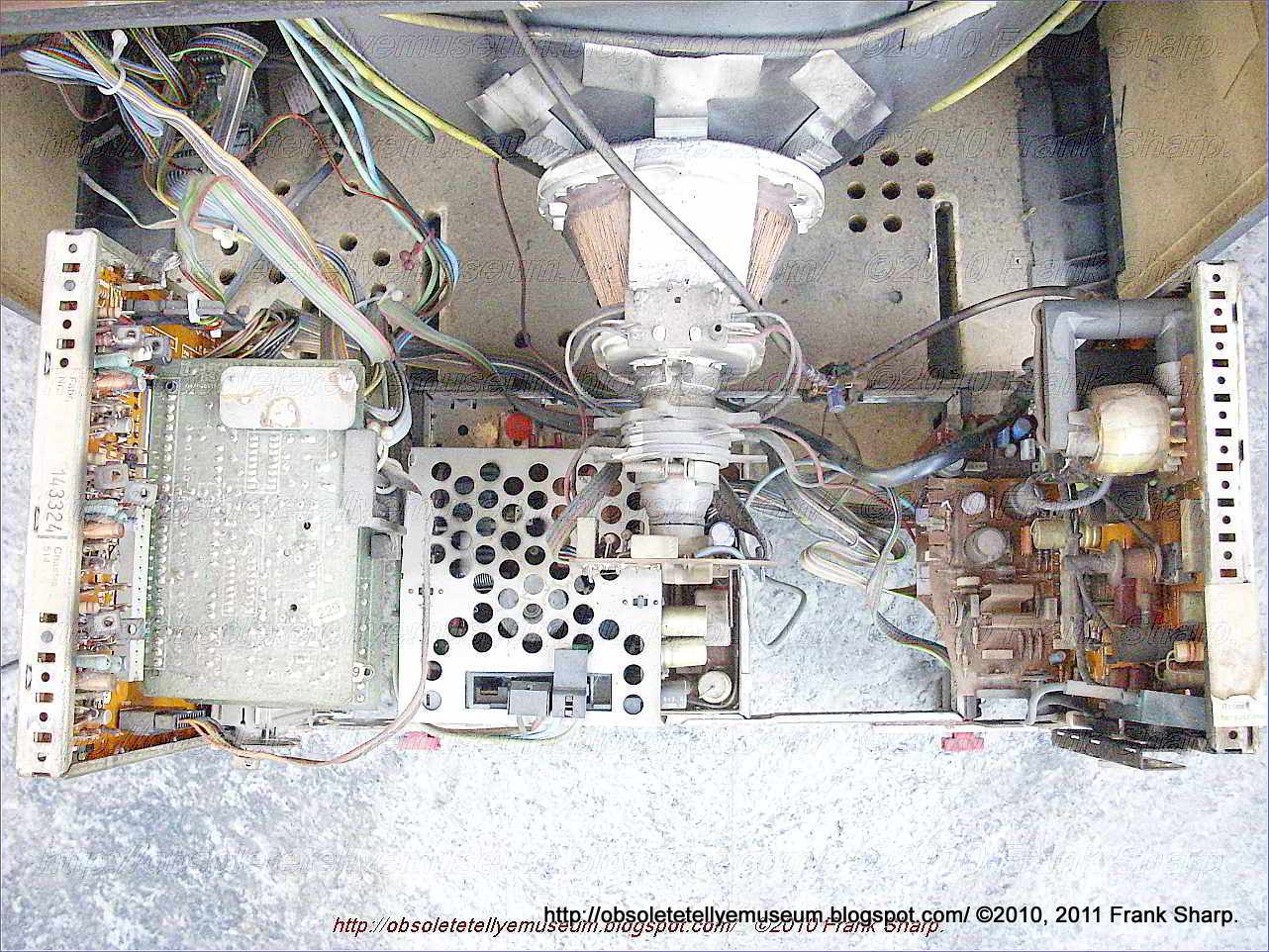


The Telefunken Chassis 514 Is the Telefunken chassis which uses the 90° degree toshiba Blackstripe crt tube and it's developed like a "book" in similar way as the Telefunken 712A and 712 and previous 711 and 714 and 714a.
Modularity is the main aspect of this chassis which was ultra reliable and gave very few problems during his very high lasting life.
It's slightly rare because of the format type.
- NETZ EINGANG BS422 MAINS INPUT ET309378996
- ANSTEUERUNG BS423 SMPS UNIT AT 349354067 WITH THOSHIBA BU208A
- SYNCHRONISIERUNG BS533 AT 349354133 WITH TDA1950
- VERTIKAL ENDSTUFE BS453 AT 349354096 WITH TDA1170
- SEC. SPANNUNGSERZEUGUNG BS426 AT349354095
- VIDEO BS 349354141 WITH TDA3560
-TON BS BS157 AT349354131
- BILD-ZF-VERST BS105 AT349354129


- ESS3 BS650 AT349354136 WITH U336M (REMOTE DECODER) +
AY-3-8210 Miscellaneous Digital Circuit - ECONOMEGA II,A digital tuning system
FEATURES
I 16/32 Program Options
I 4 Bands
I 14 Elit Tuning Resolution on B3
I Program Copying
I Non-Volatile Memory without Battery
I Manual Up/Down Tuning
I Manual Band Switching
I Mute Output at Program Selection
I Search Active Output
I Local Program Llp/Down Control
I Validate Circuitry
I Referenced Tuning Waveform Output
I Band Step Option 3/4 Select
DESCRIPTION
The Economega IIA Digital Tuning system is a voltage synthesizer
for both Ftadio and TV manual tuning applications.
The AY-3-8211 N-Channel control chip interfaces directly with an
ER140() non-volatile memory enabling storage of up to 32 programs.
Variable mark space ratio tuning information from the AY-3-8211
is amplified and filtered, and the resulting DC level used to con-
trol the TV or Radio tuner,
OPERATION
Tuning-Resolutions are as follows:
0 tlon1 Option 2
B1 (Band 1) 11 bits (16mV) 12 bits (8mV)
B2 (Band III), B4 12 bits tamv). 13 bits (4mv)
B3 (UHF) 14 bits (2rnVl 14 bits (2mV)
These are the tuning information incrementing resolutions con-
trolled bythe Tune Up/ Down, Band Inputs, and Fine Tune inputs.
Voltages relate to approximately 30 volt tuning range.
Fine Tune-The Fine Tune steps approximately 8 times per second
(related to system clock). The Fine Tune input is disabled when
searching (Band inputs pressed orTune Llp/Down active) and when
Mute is active. Tuning resolutions as above.
Scanning-The actual tuning rates, fixed bythe Tuning Clock, may
be adjusted over a wide limit. typical figures are quoted below.
Operation of a Band Input or Tune Up/Down initiates scanning on
the selected band, and the Search O/P goes low.
Typical Scan rates are as follows:
Scan 1'Ime
Band Opt|on1 Option 2
1 1.25 sec 2.5 sec
2, 4 2.5 sec 5 sec
3 10 sec 10 sec
This corresponds to a Tuning Clock of approximately 1.6KHz.
When the Tuning Output overflows, scanning pauses for 256ms to
allow time for the tuning voltage, and il in Band Step Mode, the
Band outputs to settle.
This pause occurs at the bottom ot the tuning range when tuning
up and at the top ofthe tuning range when tuning down.
Mutlng-When a program change is made, at Power ON, and
Standby to OFF, the mute output is activated for 256 msecs and
disables the Fine Tune inputsfor this time, Mute O/Pis also active
while scanning; i.e. when a Band l/P or Tune Up/Down I/P is
active.
Tuning Procedure-Three tuning procedures are available:
(a) 1. Select required program number (1 to 16 or 32).
2. Press required band button, scanning commences from
the station currently tuned, scanning stops immediately
upon release of button.
3. Fine tune if required.
4. Tuning information is stored automatically upon release
of band button or release of Fine Tune button.
5. Tuning information may be copied by pressing Copy
and selecting a new program number.
(b)With Tuning Option selected:
1. Select Band-this is latched on,
2. Tune Up or Down using Tune Up/Down Input.
3. Fine Tune if required.
4. Tuning information is stored automatically upon release
of Tune Up/Down or release of Fine Tune Up/Down.
5. A program location is selected by first pressing Copy and
then selecting the required Program number.
(c) With Band Step 3 or4 selected and Tuning Option Selected:
1. Select band-this is latched on.
2. Tune Up or Down (Tuning will now follow from band to
band).
3. Once a station is tuned, release Tu ne Up/Down and Fine
Tune, if required.
4. Tuning information is stored automatically upon release
of Tune Up/Down or release of Fine tune Up/Down.
5. A Program location is selected by first pressing copy and
then selecting required program number.
Output Signals-Tuning voltage and Band outputs are not dis-
turbed by internal sequences, for example; STORE and COPY
Only program change will disturb these outputs-program change
being either a change of band and/or tuning information.
- TUNER FOR VST SEARCH TYPE
TDA1170 vertical deflection
FRAME DEFLECTION INTEGRATED CIRCUITGENERAL DESCRIPTION f The TDA1170 and TDA1270 are monolithic integratedcircuits designed for use in TV vertical deflection systems. They are manufactured using
the Fairchild Planar* process.
Both devices are supplied in the 12-pin plastic power package with the heat sink fins bent
for insertion into the printed circuit board.
The TDA1170 is designed primarily for large and small screen black and white TV
receivers and industrial TV monitors. The TDA1270 is designed primarily for driving
complementary vertical deflection output stages in color TV receivers and industrial
monitors.
APPLICATION INFORMATION (TDA1170)
The vertical oscillator is directly synchronized by the sync pulses (positive or negative); therefore its free
running frequency must be lower than the sync frequency. The use of current feedback causes the yoke
current to be independent of yoke resistance variations due to thermal effects, Therefore no thermistor is
required in series with the yoke. The flyback generator applies a voltage, about twice the supply voltage, to
the yoke. This produces a short flyback time together with a high useful power to dissipated power ratio.
TDA1950 (itt), Line Circuits for TV Receivers (18-Pin Plastic Package)

These integrated circuits are advanced versions of the well-known types TDA1940, TDA1940F, TDA1950 and TDA1950F are identical
TBA940/950, TDA9400/9500 etc. integrated line oscillator circuits. except the following: at pin 2 the types having the suffix "F" supply ,
They comprise all stages for sync separation and line synchronisation horizontal output pulses of longer duration compared with the basic I
in TV receivers in one single silicon chip. Due to their high degree of types Integration, the number of external components is very small.
This integrated circuit contains the horizontal sweep generator (HO), the amplitude filter (AS), the sync-signal separating circuit (SA)
and the frequency/phase
comparator (FP). For the purpose of suppressing noise pulses which
are caused via the operating voltage during the upper and the
lower inversion point of the horizontal sweep generator (HO) which
contains a single capacitor (C) and a first threshold stage
circuit (SS1) with two fixed thresholds, there are provided a second
and a third threshold stage circuit (SS2, SS3), to the inputs of
which the sawtooth signal is applied, and with the thresholds
thereof, approximately 2 μs prior to reaching the upper or the
lower peak value of the sawtooth signal, are being passed through
thereby. The output signal of the second threshold circuit (SS2)
and the output signal of the third threshold stage circuit (SS3)
which is applied via the pulse shaper circuit (IF), are
superimposed linearly and, via the stopper circuit (blocking
stage) (SP) serve to control the application of the composite
video signal (BAS) to the amplitude filter (AS), or else they are
applied to a clamping circuit which serves to apply the operating
points of the amplitude filter (AS) and/or of the sync-signal
separating circuit (SA) to such a potential that these two stages,
for the time duration of these output pulses, are prevented from
operating.1. An integrated circuit for color television receivers, comprising a voltage- or current-controlled horizontal sweep generator (HO), an amplitude filter (AS), a synchronizing-signal separating circuit (SA) and a frequency/phase comparator (FP) which serves to synchronize the horizontal sweep generator (HO), with said generator being a sawtooth generator containing a single capacitor
(C) and a first threshold stage circuit (SS1) having two fixed thresholds, said integrated circuit further comprising:a second and a third threshold stage circuit (SS2, SS3) each being supplied with the sawtooth signal on the input side, comprising each time one threshold which, approximately 2μs prior to the reaching of the upper or the lower peak value of the sawtooth signal, is being passed thereby;
a pulse shaper circuit (IF) coupled to the output of said third threshold stage circuit (SS3) which pulse shaper circuit reduces the duration of the output pulse thereof to about the duration of the output pulse of said second threshold stage circuit (SS2), and
a stopper circuit (blocking stage) (SP) coupled to the outputs of both said pulse shaper circuit (IF) and said second threshold stage circuit (SS2), said stopper circuit having a signal input to which there is applied a composite video signal (BAS) and a signal output which is coupled to the input of said amplitude filter (AS).
2. The invention of claim 1 wherein the outputs of both said pulse shaper circuit (IF) and said second threshold stage circuit (SS2) are coupled to a clamping circuit which applies the operating points of said amplitude filter (AS) and said sync-separating signal (SA) to such a potential that they are prevented from operating.
3. An integrated horizontal sweep circuit comprising:
a generator for generating a sawtooth signal;
an amplitude filter having an input for receiving a composite video signal and having an output;
a sync-signal separating circuit having an input coupled to said amplitude filter output and having an output;
a frequency/phase comparator having a first input coupled to said separating circuit output,
a second input receiving said sawtooth signal and an output for controlling said generator; and
a control circuit responsive to said sawtooth signal for inhibiting said composite video signal when said sawtooth signal is within predetermined signal level ranges about the upper and lower inversion points of said sawtooth signal.
4. An integrated circuit in accordance with claim 3 wherein:
said generator comprises a capacitor, circuit means for charging and discharging said capacitor, and a first threshold circuit controlling said circuit means in response to said sawtooth signal reaching a first level corresponding to said first inversion point and a second level corresponding to said second inversion point.
5. An integrated horizontal sweep circuit comprising:
a sawtooth signal generator;
an amplitude filter having an input receiving a composite video signal and having an output;
a sync-signal separating circuit having an input coupled to said amplitude filter output and having an output;
a frequency/phase comparator having a first input coupled to said separating circuit output, a second input receiving said sawtooth signal and an output for controlling said generator; and
a control circuit responsive to said sawtooth signal for inhibiting operation of said amplitude filter and/or said sync-signal separating circuit when said sawtooth signal is within predetermined signal level ranges about the upper and lower inversion point of said sawtooth signal.
6. An integrated circuit in accordance with claim 5 wherein:
said generator comprises a capacitor, circuit means for charging and discharging said capacitor and a first threshold circuit controlling said circuit means in response to said sawtooth signal reaching a first level corresponding to said first inversion point and a second level corresponding to said second inversion point.
Description:
BACKGROUND OF THE INVENTIONThe invention relates to an integrated circuit for (color) television receivers, comprising a voltage- or current-controlled horizontal-sweep generator, an amplitude filter, a synchronizing signal separating circuit (sync-separator) and a frequency/phase comparator which serves to synchronize the horizontal sweep generator which is a sawtooth generator consisting of a single capacitor and of a first threshold stage having two fixed switching thresholds, cf. preamble of the patent claim. Such types of integrated circuits, for example, are known from th
e technical journal "Elektronik aktuell", 1976, No. 2, pp. 7 to 14 where they are referred to as TDA 9400 and TDA 9500.Especially on account of the fact that the amplitude filter as well as the horizontal sweep generator in the form of the aforementioned sawtooth generator, are integrated on a single semiconductor body, it is likely that noise interference pulses coming from the individual stages, and via the supply voltage line, may have a disturbing influence upon the horizontal sweep generator, i.e. upon the threshold stage thereof, in such a way that either the lower or the upper or successively both switching thresholds are exceeded before the time by the voltage at the capacitor, owing to the noise superposition, so that the generator will show to have a "wrong" frequency or phase position. This frequency/phase variation, of course, is compensated for by the circuit, with the aid of the synchronzing pulses, but only in such a way that the noise effect remains visible in the television picture.
SUMMARY OF THE INVENTION
The invention is characterized in the claim is aimed at overcoming this drawback by solving the problem of designing an integrated circuit of the type described in greater detail hereinbefore, in such a way that noise pulses acting upon the capacitor voltage or the internal reference voltages for the switching thresholds (see below) in the proximity of the two switching thresholds, are prevented from having the described disadvantageous effect. Accordingly, an advantage of the invention results directly from solving the given problem.
Other objects, features and advantages of the present invention will become more fully apparent from the following detailed description of the preferred embodiment, the appended claims and the accompanying drawing in which:
BRIEF DESCRIPTION OF THE INVENTION
The invention will now be described in greater detail with reference to the accompanying drawing. This drawing, in the form of a schematical circuit diagram, shows the construction of an integrated circuit according to the invention.
DETAILED DESCRIPTION OF THE INVENTION
T
he
horizontal sweep generator HO comprises the capacitor C as
connected to the zero point of the circuit, and which is charged and
discharged via the two shown constant current sources CS1 and
CS2, thus causing the intended sawtooth voltage to appear thereat.
Moreover, the horizontal sweep generator HO comprises the first
threshold stage circuit SS1, having an upper and a lower threshold.
As soon as the capacitor voltage exceeds one of the thresholds,
the first threshold stage circuit SS1 switches over to the other
threshold. The two thresholds are defined by the voltage divider P
as connected to the operating voltage U, and in which the
corresponding threshold inputs are connected to corresponding
tapping points. The output of the threshold stage circuit SS1
controls the electronic switch S, so that the constant current
source CS2 as connected thereto, is either disconnected from or
connected to the zero point of the circuit. Accordingly, in the
disconnected state, the capacitor C is charged via the constant
current source CS1 arranged in series therewith while in the
connected state the capacitor C is discharged across the
aforementioned constant current source CS2 arranged in parallel
therewith, if, as a matter of fact, the current of the constant
current source CS1 arranged in series with the capacitor C, is
smaller than that of the parallel-arranged constant current source
CS2.Now, for the purpose of avoiding the aforementioned drawbacks, there is provided a second and a third threshold stage circuit SS2 and SS3, respectively, as well as the pulse shaper circuit IF. To the respective input of the two threshold stage circuits SS2, SS3, there is applied the capacitor voltage, in the form of the sawtooth signal, and these stages have a threshold voltage which, approximately 2 μs prior to the reaching of the upper or the lower peak value of the sawtooth voltage, is being passed thereby. This means to imply that the threshold voltage of the second threshold stage circuit SS2 is somewhat lower than the voltage of the upper threshold of the first threshold stage circuit SS1, and that the threshold voltage of the third threshold stage circuit SS3 is somewhat higher than the voltage of the lower threshold of the first threshold stage circuit SS1. The two thresholds of the threshold stage circuits SS2, SS3 can thus be realized in a simple way by providing further tapping points at the voltage divider P, as is shown in the accompanying drawing. Thus, the second threshold stage circuit SS2 is provided for at a voltage divider tapping point below the tapping point chosen for the upper threshold, and the tapping point for the third threshold stage circuit SS3 is provided for above the tapping point which has been chosen for the lower threshold of the first threshold stage circuit SS1.
Since, within the area of the lower inversion point of the sawtooth signal there results an excessively wide output pulse of the third threshold stage circuit SS3, the pulse shaper circuit IF is arranged subsequently thereto, for reducing the duration of the output pulse as applied to its input, to about the duration of the output pulse of the second threshold stage circuit SS2. This pulse shaper circuit IF, for example, may be realized by a monoflop, in particular by a digital monoflop (=monostable circuit).
The output pulses of the second threshold stage circuit SS2 and of the pulse shaper circuit IF are then super-positioned linearly, with th
is being denoted in
the drawing by a simple interconnection of the two respective
lines. The combined signal is applied to the input of the stopper
circuit (blocking stage) SP, to the signal input of which there is
fed the composite video signal BAS, and the output thereof
controls both the amplitude filter AS and the synchronizing signal
separating circuit SA.The combined signal may also be used to control a clamping circuit applying the operating points of the amplitude filter AS and/or of the sync-signal-separating circuit SA to such a potential which prevents it from operating.
If now the sawtooth signal reaches the range of its upper or its lower inversion point, the composite video signal BAS is not applied to either the amplitude filter AS or the sync-signal separating circuit SA, so that shortly before and shortly after the inversion points, signals are prevented from being processed in the two stages AS, SA. This, in turn, has the consequence that during these times noise pulses are prevented from superimposing upon the operating voltage U, so that there is also prevented an unintended triggering of the first threshold stage circuit SS1.
Moreover, it is still shown in the drawing that the amplitude filter AS, the sync-signal separating circuit SA and the frequency/phase comparator FP are arranged in series in terms of signal flow, with the latter, in addition, receiving the sawtooth signal, and with the output signal thereof acting upon the two current sources in a regulating sense. In the drawing, this is indicated by the setting arrows at the two current sources.
While the present invention has been disclosed in connection with the preferred embodiment thereof, it should be understood that there may be other embodiments which fall within the spirit and scope of the invention as defined by the following claims.
BU208(A)
Silicon NPNnpn transistors,pnp transistors,transistors
Category: NPN Transistor, Transistor
MHz: <1 MHz
Amps: 5A
Volts: 1500V
HIGH VOLTAGE CAPABILITY
JEDEC TO-3 METAL CASE.
DESCRIPTION
Th
e BU208A, BU508A and BU508AFI aremanufactured using Multiepitaxial Mesa
technology for cost-effective high performance
and use a Hollow Emitter structure to enhance
switching speeds.
APPLICATIONS:
* HORIZONTAL DEFLECTION FOR COLOUR TV With 110° or even 90° degree of deflection angle.
ABSOLUTE MAXIMUM RATINGS
Symbol Parameter Value Unit
VCES Collector-Emit ter Voltage (VBE = 0) 1500 V
VCEO Collector-Emit ter Voltage (IB = 0) 700 V
VEBO Emitter-Base Voltage (IC = 0) 10 V
IC Collector Current 8 A
ICM Collector Peak Current (tp < 5 ms) 15 A
TO - 3 TO - 218 ISOWATT218
Ptot Total Dissipation at Tc = 25 oC 150 125 50 W
Tstg Storage Temperature -65 to 175 -65 to 150 -65 to 150 oC
Tj Max. Operating Junction Temperature 175 150 150 °C
TELEFUNKEN PALCOLOR 5808J Supercontrol CHASSIS 514 Drive circuit for an infrared remote control transmitter:
An infrared remote control transmitter includes at least one infrared light-emitting diode poled with respect to a point of reference potential so as to be conductive in response to voltages having the opposite polarity of a DC supply voltage and to be nonconductive in response to voltages having the same polarity as the DC supply voltage. A push-pull amplifier is responsive to a pulse signal encoded to represent a remote control message to selectively couple the DC supply voltage or the reference potential to a capacitor coupled in series between the push-pull amplifier and the light-emitting diode. The capacitor is charged and discharged and an alternating drive voltage for the light-emitting diode having portions with polarities both the same as and opposite to the polarity of the DC supply voltage is generated. The push-pull amplifier is arranged so that when a component failure occurs, the portions of the alternating drive voltage having the polarity opposite to the polarity of the DC supply voltage are at least inhibited to prevent the continuous (i.e., DC) emission of infrared radiation.
 1. In an infrared remote control transmitter for controlling a television system, apparatus comprising:
 a reference circuit point for receiving a reference potential;
a supply circuit point for receiving a DC supply voltage;
a battery connected with a predetermined polarity connected between said supply and reference circuit points;
at least one light-emitting diode for emitting infrared radiation when rendered conductive, said light emitting diode having a cathode and an anode, one of said cathode and anode being connected to said reference circuit point, said light-emitting diode being poled with respect to said reference circuit point so as to be conductive in response to the application of a voltage to the other one of said cathode and anode having the opposite polarity to said battery with respect to said reference circuit point and non-conductive in response to the application of a voltage to said other one of said cathode and anode having the same polarity as said battery with respect to said reference circuit point;
a source cir
a drive circuit point;
a capacitor directly connected between said drive circuit point and said other one of said cathode and anode;
a diode directly connected between said other one of said cathode and anode and said reference circuit point and poled in the opposite sense to said light-emitting diode with respect to said reference circuit point;
push-pull amplifier means for developing a drive voltage at said drive point including first and second bipolar transistors of opposite conduction types, each of said transistors having a collector-emitter path and a base electrode for controlling the conduction of said collector-emitter path, said collector-emitter path of said first transistor being directly connected between said supply circuit point and said drive circuit point, said collector-emitter path of said second transistor being connected between said drive circuit point and said reference point; and
input means coupled between said source circuit point and said bases of said first and second transistors for rendering said collector-emitter path of said first transistor conductive and said collector-emitter path of said second transistor non-conductive in response to a first portion of said pulses of said input signal and for rendering said collector-emitter path of said second transistor conductive and said collector-emitter path of said first transistor non-conductive in response to a second portion of said pulses of said input signal.
2. The apparatus recited in claim 1 wherein:
three light-emitting diodes poled in the same direction are connected in series between said capacitor means and said reference circuit point.
3. The apparatus recited in claim 1 wherein:
a second capacitor is directly connected between said drive point and said other one of said cathode and anode in parallel with said first mentioned capacitor directly connected between said drive point and said other one of said cathode and anode.
4. The apparatus recited in claim 1 wherein:
said input means includes a first capacitor connected between said source circuit point and said base of said first transistor; first means connected between said supply circuit point and said base of said first transistor for discharging said first capacitor; a second capacitor connected between said source circuit point and said base of said second transistor; and second means connected between said base of said second transistor and said reference circuit point for discharging said second capacitor.
5. The apparatus recited in claim 4 wherein:
said first means includes a further diode poled to be conductive when said collector-emitter path of said first transistor is non-conductive and non-conductive when said collector-emitter path of said first transistor is conductive; and
said second means includes a still further diode poled to be conductive when said collector-emitter path of said second transistor is non-conductive and non-conductive when said collector-emitter path of said second transistor is conductive.
6. In an infrared remote control transmitter for controlling a television system, apparatus comprising:
a reference circuit point for receiving a reference potential;
a supply circuit point for receiving a DC supply voltage;
a battery connected with a predetermined polarity connected between said supply and reference circuit points;
three light-emitting diodes which emit infrared radiation when rendered conductive directly connected in series between a voltage application circuit point and said reference circuit point, all of said light-emitting diodes being poled with respect to said reference circuit point so as to be conductive in response to the application of a voltage to said voltage application circuit point having the opposite polarity to said battery with respect to said reference circuit point and non-conductive in response to the application of a voltage to said voltage application circuit point having the same polarity as said battery with respect to said reference circuit point;
a source circuit point for receiving an input signal having pulses encoded to represent information for controlling a predetermined function of said television receiver;
a drive circuit point;
a first capacitor directly connected between said drive circuit point and said voltage application circuit point;
a second capacitor directly connected between said drive circuit point and said voltage application circuit point;
a diode directly connected between said voltage application circuit point and said reference circuit point and poled in the opposite sense to said light-emitting diode with respect to said reference circuit point;
input means coupled between said source circuit point and said bases of said first and second transistors for rendering said collector-emitter path of said first transistor conductive and said collector-emitter path of said second transistor non-conductive in response to a first portion of said pulses of said input signal and for rendering said collector-emitter path of said second transistor conductive and said collector-emitter path of said first transistor non-conductive in response to a second portion of said pulses of said input signal.
Description:
BACKGROUND OF THE PRESENT INVENTION
The present invention relates to drive circuits for infrared remote control transmitters.
Infrared remote control systems for television receivers and the like are known. The chief advantage of infrared remote control systems in comparison to ultrasonic remote control systems is that they are less susceptible to erroneously-generated interference signals. Unfortunately, the human eye may be harmed under conditions of prolonged, continuous and direct exposure to infrared radiation.
In order to reduce the possibility of harm to the eyes of users, infrared remote control systems utilize special pulse codes which minimize the duration of infrared radiation during the transmission of remote controlled messages. However, since in conventional drive circuits for infrared remote control transmitters the infrared light source, e.g., a light-emitting diode or diodes, is typically included in a direct current path from a supply voltage, infrared radiation may be continuously emitted should there be a component failure in the remote control transmitter. Therefore, there is a requirement for drive circuits for use in infrared remote control transmitters in which component failures do not result in the continuous emission of infrared radiation. The present invention concerns such a "fail-safe" drive circuit.
SUMMARY OF THE PRESENT INVENTION
In a remote control transmitter, at least one infrared light-emitting diode is coupled to a point of reference potential and poled so as to be substantially nonconductive in response to voltages having the same polarity as a DC supply voltage for the transmitter and substantially conductive in response to voltages having the polarity opposite to the polarity of the DC supply voltage. Driver means responsive to an input signal is coupled between the source of the DC supply voltage and the light-emitting diode. The driver means normally generates an alternating drive voltage for the light-emitting diode having portions with polarities both the same as and opposite to the polarity of the DC supply voltage. The driver means is arranged so that the portions of the drive signal having the polarity opposite to that of the DC supply voltage are at least inhibited when a component failure occurs.
BRIEF DESCRIPTION OF THE DRAWING
The sole FIGURE of the drawing shows, partially in block diagram form and partially in schematic diagram form, an infrared remote control system constructed in accordance with the present invention as it may be employed in a television receiver arrangement.
DETAILED DESCRIPTION OF THE DRAWING
A tele vision receiver 1 includes an antenna 3, a tuner 5, an IF signal processing unit 7, a picture signal processing unit 9, a sound signal processing unit 11, a picture tube 13 and a speaker 15 arranged in a conventional fashion to produce visual and audio responses. A power supply 17 is selectively energized to generate DC supply voltages for the portions of the receiver so far described from the AC line voltage in response to an ON/OFF control signal generated by a remote control receiver 19. Receiver 1 also includes a standby power supply 20 which continuously couples a DC supply voltage to remote control receiver 19 so that it is ready to accept messages from a remote control transmitter 21.
Remote control receiver 19 includes a photosensitive diode 23. The conduction of photo diode 23 is controlled in response to encoded optical signals having frequencies in the infrared range generated by remote control transmitter 21. A detector 25 senses the changes in the conduction of diode 23 and generates electrical signals corresponding to the encoded optical signals. The electrical signals are decoded by a decoder 27 to generate the ON/OFF control signal for tuning receiver 1 on and off, a CHANNEL SELECTION control signal for controlling the frequency to which a tuner 5 is tuned, and a VOLUME control signal for controlling the sound level of receiver 1.
Remote control transmitter 21 includes a keyboard 29 including push buttons (not shown) by which a user may control the various receiver functions enumerated above. When a push button is depressed a corresponding electrical signal is generated by keyboard 29. A pulse encoder 31 is responsive to these electrical signals to generate respective coded pulse signals. The coded pulse signals are processed by a driver 33 to cause infrared light-emitting diodes 35, 37 and 39 to generate corresponding optical signals in the infrared frequency range.
Various codes for infrared remote control systems and encoders and decoders for these codes are known. For example, encoder 31 and decoder 27 may comprise S2600 and S2601 integrated circuits manufactured by American Microsystems, Inc. of Santa Clara, Calif.
The exact nature of the codes is not directly germane to the present invention. However, it is desirable for the reasons of safety discussed earlier that the code formats are arranged so that the duration of infrared radiation during a transmission is minimized. Since the pulses of the pulse signals generated by pulse encoder 31 correspond to the intervals of infrared radiation, this may be accomplished by causing the electrical pulse signals generated by encoder 31 to have a relatively low duty cycle, e.g., less than 20 percent. In addition, for safety reasons, it is desirable that light-emitting diodes 35, 37 and 39 be physically separated on transmitter 21 from one another by a distance selected so that the power of the infrared radiation they generate is distributed rather than concentrated in a relatively small area.
While these safety precautions to some extent minimize the danger to users, they do not account for component failures which may cause the continuous, i.e., DC, emission of infrared radiation. Unfortunately, the human eye may be injured when directly exposed to continuous infrared radiation for prolonged periods. While such situations are extremely rare, since they would involve not only a component failure but the misuse of the transmitter, they may occur under extraordinary circumstances. For example, a curious child may point an infrared transmitter with a failed component directly into his eye.
Drive circuit 33 is arranged to prevent the continuous emission of infrared radiation under any foreseeable component failure mode. Driver 33 includes a push-pull amplifier 41 comprising a PNP transistor 43 and an NPN transistor 45 having their collector-emitter junctions coupled in series between a battery 47 and signal ground. Battery 47 is the source of DC supply voltage for transmitter 21. The output of pulse encoder 31 is coupled to the bases of transistors 43 and 45 through capacitors 49 and 51, respectively. Diodes 53 and 55 are coupled in shunt with the base-emitter junctions of transistors 43 and 45, respectively. The junction of the collectors of transistors 43 and 45 is coupled through parallel connected capacitors 57 and 58 to the cathode of light-emitting diode 35. Light-emitting diodes 35, 37 and 39 are connected in series with the same polarity between capacitors 57 and 58 and signal ground. The polarity of light-emitting diodes 35, 37 and 39 is selected so that they are rendered nonconductive in response to the application of voltages to the cathode of light-emitting diode 35 having the same polarity (i.e., positive) with respect to signal ground as the DC supply voltage provided by battery 47 and only rendered conductive in response to the application of voltages having the opposite polarity (i.e., negative) with respect to signal ground to the DC supply voltage. A diode 59 is connected in shunt with series connected light-emitting diodes 35, 37 and 39 and poled in the opposite direction.
In operation, pulse encoder 31 generates a pulse signal encoded as described above. The pulse signal includes positive-going pulses. In response to the leading edges of the positive-going pulses, transistor 45 is rendered conductive. In response to the trailing edges of the positive-going pulses, transistor 43 is rendered conductive. Diodes 53 and 55 serve as discharge paths for capacitors 49 and 51 during the intervals when transistors 43 and 45, respectively, are nonconductive. Diodes 53 and 55 also clamp the voltage at the bases of transistors 43 and 45 close to the battery voltage and the voltage at signal ground, respectively, in order to protect the base-emitter junctions of transistors 43 and 45 from reverse breakdown failure voltages. Desirably, capacitors 49 and 51 have relatively small values so that capacitors 49 and 51 are charged and discharged in response to each pulse. As a result, transistors 43 and 45 are alternately rendered conductive and nonconductive in response to each pulse of the pulse signal.
When transistor 43 is conductive (and transistor 45 is nonconductive) capacitors 57 and 58 are charged from battery 47. When transistor 45 is conductive (and transistor 43 is nonconductive) capacitors 57 and 58 are discharged to signal ground. As a result, an alternating drive voltage, i.e., one having polarity excursions above and below the potential at signal ground, are generated at the cathode of light-emitting diode 35. Light-emitting diodes are conductive in response to the negative portions of the drive voltage and are nonconductive in response to the positive portions of the drive voltage. Diodes 35, 37 and 39 only emit infrared radiation when they are conductive. Therefore, infrared radiation is only emitted by transmitter 21 when the drive voltage has a polarity (i.e., negative opposite to the polarity of the DC supply voltage.
Desirably, the capacitance of the combination of capacitors 57 and 58 is relatively large, e.g., 1 microfarad, so that sufficient drive current is provided to light-emitting diodes 35, 37 and 39 to cause them to emit infrared radiation. For the same reason, two capacitors rather than one are used, since the effective series resistance associated with the parallel combination is smaller than the series resistance of a single capacitor.
In the event that there is a component failure within drive circuit 33, drive voltage developed at the cathode of light-emitting diode 35 will be reduced and, in most cases, substantially inhibited. Under these conditions, since the amplitude of the negative portions of the drive signal will at least have a lower than normal amplitude, the infrared radiation will have a lower than normal energy.
Briefly, any failure of a component within driver 33 causing the component to open or short, substantially prevents the development of an alternating drive signal at the cathode of light-emitting diode 35. Since diodes 35, 37 and 39 are rendered conductive only in response to negative-going voltages, no infrared radiation is generated. Any component failure between the extremes of an open or short causes a reduction in the amplitude of the alternating drive signal. By way of example, consider the following failure modes. If either transistor 43 or 45 fails, e.g., by shorting from collector to emitter, capacitors 57 and 58 will be either permanently charged or discharged, thereby preventing the development of an alternating drive signal. If one of capacitors 57 and 58 shorts, only positive-going voltages are developed at the cathode of light-emitting diode 35. If the collector to emitter junction of transistor 43 and one of capacitors 57 and 58 short, a DC signal is coupled to the cathode of light-emitting diode 35, thereby rendering diode 59 conductive and preventing light-emitting diodes 35, 37 and 39 from being rendered conductive. If diode 59 opens, capacitors 57 and 58 will not be charged thereby preventing the development of an alternating voltage at the cathode of diode 35. If diode 59 fails so as to lose its unidirectional conductive characteristics, i.e., in essence becomes a passive element, an alternating drive signal will be developed but it will have a lower than normal amplitude. Furthermore, failures in pulse encoder 31 causing generation of a DC signal rather than a pulse signal will also cause the loss of an alternating drive signal.
Driver circuit 33 may be modified in some respects without causing the loss of its "fail-safe" nature. For example, any or all of diodes 53, 55 and 59 may be replaced with resistors. While this modification causes a reduction in efficiency of the normal operation of drive circuit 33, it does not alter its "fail-safe" nature. These and other modifications are intended to be within the scope of the present invention as set forth in the following claims.
TELEFUNKEN CHASSIS 514 (AT349354097) Switching power supply, especially for a T.V. receiving apparatus:
 1. Switch mode power supply means, especially for a television receiver,
having a working winding (5), a switching transistor (6), a
back-coupling winding (7) and a control switch (11) on the primary side
of a divided transformer (1), and also having rectifiers (15, 16, 20)
for the production of the drive voltages (U1, U2, U3) on the secondary
side of the transformer (1), characterized by the following features :
(a) Connected to a winding (19) there is a thyristor (24) which is poled
in the permitted direction for the voltage at the winding (19) arising
during the current conducting phase of the switching transistor (6). (b)
One of the drive voltages (U2) is applied to the control electrode of
the thyristor (24) with such magnitude that the thyristor (24) remains
blocked in the normal working state and fires on the occurrence of an
inadmissible rise of the drive voltage (U3).
1. Switch mode power supply means, especially for a television receiver,
having a working winding (5), a switching transistor (6), a
back-coupling winding (7) and a control switch (11) on the primary side
of a divided transformer (1), and also having rectifiers (15, 16, 20)
for the production of the drive voltages (U1, U2, U3) on the secondary
side of the transformer (1), characterized by the following features :
(a) Connected to a winding (19) there is a thyristor (24) which is poled
in the permitted direction for the voltage at the winding (19) arising
during the current conducting phase of the switching transistor (6). (b)
One of the drive voltages (U2) is applied to the control electrode of
the thyristor (24) with such magnitude that the thyristor (24) remains
blocked in the normal working state and fires on the occurrence of an
inadmissible rise of the drive voltage (U3).
TELEFUNKEN PALCOLOR CHASSIS 514 Schaltnetzteil AT349354097
(AT 349354097), IN GERMAN:
1. Schaltnetzteil,
insbesondere f·ur einen Fernsehempf·anger, mit einer Arbeitswicklung
(5), einem Schalttransistor (6), einer R·uckkopplungswicklung (7) und
einer Regelschaltung (ii) auf der Prim·arseite sowie mit Gleichrichtern
(15,16, 20) zur Erzeugung von Betriebsspannungen (U11U2#U3) auf der
Sekund·arseite eines Trenntransformators (1) gekenn zeichnet durch
folgende Merkmale: a) An eine Wicklung (19) ist ein Thyristor (24)
angeschlos sen, der f·ur die w·ahrend der siromf·uhrenden Phase der
Schalttransistoren (6) an der Wicklung (19) auftreten de Spannung in
Durchlassrichtung gepolt ist. b) An die Steuerelektrode des Thyristors
(24) ist eine der Betriebsspannungen (U2) in solcher H·ohe angelegt,
dass der Thyristor (24) im Normalbetrieb gesperrt bleibt und bei einem
unzul·assigen Anstieg der Betriebs spannung (U3) z·undet.

2. Netzteil nach Anspruch 1, dadurch gekennzeichnet, dass die Betriebsspannung (U3) ·uber einen Spannungsteiler (25,26) an die Steuerelektrode des Thyristors (24) angelegt ist.
3. Netzteil nach Anspruch 1, dadurch gekennzeichnet, dass die Wicklung (19) eine Sekund·arwicklung des Trenntransforma tors (1) ist.
 Schaltnetzteil, insbesondere f·ur einen Fernsehempf·anger
Bei Ger·aten der Nachrichtentechnik wie z.B. einem Fernsehempf·anger ist es bekannt, die f·ur die einzelnen Stufen notwendigen Betriebsspannungen mit einem Schaltnetzteil aus der Netzspannung zu erzeugen (Funkschau 1975, Heft 5, Seite 40-43). Ein Schaltnetzteil erm·oglicht die f·ur den Anschluss ·ausserer Ger·ate und f·ur die Massnahmen zur Schutzisolierung vorteilhafte galvanische Trennung der Empf·angerschaltung vom Netz. Da ein Schaltnetzteil mit einer gegen·uber der Netzfrequenz hohen Frequenz von ca. 30 kHz arbeitet, kann der zur galvanischen Trennung dienende Trenntransformator gegen·uber einem Netztrafo f·ur 50 Hz wesentlich kleiner und leichter ausgebildet sein. Durch mehrere Wicklungen oder Wicklungsabgriffe und angeschlossene Gleichrichter k·onnen auf der Sekund·arseite des Trenntransformators Betriebs~ spannungen unterschiedlicher Gr·osse und Polarit·at erzeugt werden.
 Ein
solches Schaltnetzteil enth·alt eine Regelschaltung zur Stabilisierung
der Amplitude der auf der Sekund·arseite erzeugten Betriebsspannungen.
In dieser Regelschaltung wird eine durch Gleichrichtung der
Impulsspannung am Trafo gewonnene Stellgr·osse erzeugt und mit einer
Bezugsspannung verglichen. In Abh·angigkeit von der Abweichung wird der
Schaltzeitpunkt des auf der Prim·arseite vorgesehenen elektronischen
Schalters so gesteuert, dass die Amplitude der erzeugten
Betriebsspannungen konstant bleibt.
Ein
solches Schaltnetzteil enth·alt eine Regelschaltung zur Stabilisierung
der Amplitude der auf der Sekund·arseite erzeugten Betriebsspannungen.
In dieser Regelschaltung wird eine durch Gleichrichtung der
Impulsspannung am Trafo gewonnene Stellgr·osse erzeugt und mit einer
Bezugsspannung verglichen. In Abh·angigkeit von der Abweichung wird der
Schaltzeitpunkt des auf der Prim·arseite vorgesehenen elektronischen
Schalters so gesteuert, dass die Amplitude der erzeugten
Betriebsspannungen konstant bleibt.
Bei einem solchen Schaltnetzteil kann die genannte Regelschaltung z.B. durch ein fehlerhaftes Bauteil ausfallen. Die Regelung der Amplitude der erzeugten Betriebsspannungen ist dann unkontrolliert. Die Betriebsspannungen k·onnen dann auf den doppelten oder dreifachen Wert ansteigen. Dadurch besteht die Gefahr, dass das Schaltnetzteil oder die an die Betriebsspannungen angeschlossenen Verbraucher wie z.B. der Heizfaden der Bildr·ohre oder der Zeilenendstufentransistor zerst·ort werden. Der Anstieg der Betriebsspannungen kann dar·uberhinaus einen Anstieg der im Fernsehempf·anger erzeugten Hochspannung und dadurch eine R·ontgenstrahlung ausl·osen.
Es ist auch ein Schaltnetzteil bekannt (DE-OS 27 27 332), bei dem zum Schutz gegen einen zu starken Anstieg der erzeugten Betriebsspannungen aus der Impulsspannung an der Prim·arseite des Trafos eine Stellgr·osse gewonnen wird, die beim ·Uberschreiten eines Schwellwertes den R·uckkopplungsweg unwirksam steuert. Durch die Unterbrechung des R·uckkopplungsweges kann das Schaltnetzteil nicht mehr schwingen, so dass in erw·unschter Weise auch keine Betriebsspannungen mehr erzeugt werden. Diese Schaltung erfordert jedoch eine Vielzahl von Bauteilen und ist daher relativ teuer.
Der Erfindung liegt die Aufgabe zugrunde, eine sicher wirkende Schutzschaltung mit verringertem Schaltungsaufwand gegendie oben
beschriebenen Gefahren zu schaffen.
Diese Aufgabe wird durch die im Anspruch 1 beschriebene Erfindung gel·ost. Vorteilhafte Weiterbildungen der Erfindung sind in den Unteranspr·uchen beschrieben.
Die Erfindung beruht auf folgender ·Uberlegung: Der Schalttransistor auf der Prim·arseite wird von der prim·arseitigen R·uckkopplungswicklung w·ahrend seiner stromleitenden Phase mit einem Basisstrom angesteuert. Wenn jetzt eine Sekund·arwicklung w·ahrend dieser stromleitenden Phase stark belastet, z.B. ·uber den Thyristor kurzgeschlossen wird, bricht auch die Spannung an der prim·arseitigen R·uckkopplungswicklung zusammen. Diese Wicklung kann dann f·ur den Schalttransistor nicht mehr einen f·ur den leitenden Betrieb ausreichenden Basis strom liefern. Das Schaltnetzteil schwingt dann nicht mehr, so dass die sekund·arseitigen Betriebsspannungen in erw·unschter Weise zusammenbrechen. Der schaltungstechni- sche Aufwand ist gering. Er besteht vorzugsweise aus einem Thyristor und zwei Widerst·anden.
Ein Ausf·uhrungsbeispiel der Erfindung wird anhand der Zeichnung erl·autert. Darin zeigen Figur 1 ein erfindungsgem·ass ausgebildetes Schaltnetzteil und Figur 2 Kurven zur Erl·auterung der Wirkungsweise. Dabei zeigen die kleinen Buchstaben, an welchen Punkten in Figur 1 die Spannungen gem·ass Figur 2 stehen.
 Das
Schaltnetzteil gem·ass Figur 1 enth·alt auf der Prim·arseite des
Trenntransformators 1 den Netzgleichrichter 2, den Ladekondensator 3,
den Strom-Messwiderstand 4, die Prim·arwicklung 5 den Schalttransistor
6, die zur Schwingungserzeugung dienende R·uckkopplungswicklung 7, den
zur Steuerung des Schalttransistors 6 dienenden Thyristor 8, die
Regelwicklung 9, den zur Erzeugung der Regelspannung dienenden
Gleichrichter 10 sowie die zur Stabilisierung der Betriebsspannungen
dienende Regelschaltung 11 mit dem Transistor 12 und der eine
Referenzspannung lieferndenZenerdiode 13. Die Sekund·arwicklung 14
liefert ·uber den Gleichrichter 15 eine erste Betriebsspannung U1 von
150 V. Ein Abgriff der Wicklung 14 liefert ·uber den Gleichrichter 16
eine zweite Betriebsspannung U2 von 12 V f·ur einen
Fernbedienungsempf·anger.
Das
Schaltnetzteil gem·ass Figur 1 enth·alt auf der Prim·arseite des
Trenntransformators 1 den Netzgleichrichter 2, den Ladekondensator 3,
den Strom-Messwiderstand 4, die Prim·arwicklung 5 den Schalttransistor
6, die zur Schwingungserzeugung dienende R·uckkopplungswicklung 7, den
zur Steuerung des Schalttransistors 6 dienenden Thyristor 8, die
Regelwicklung 9, den zur Erzeugung der Regelspannung dienenden
Gleichrichter 10 sowie die zur Stabilisierung der Betriebsspannungen
dienende Regelschaltung 11 mit dem Transistor 12 und der eine
Referenzspannung lieferndenZenerdiode 13. Die Sekund·arwicklung 14
liefert ·uber den Gleichrichter 15 eine erste Betriebsspannung U1 von
150 V. Ein Abgriff der Wicklung 14 liefert ·uber den Gleichrichter 16
eine zweite Betriebsspannung U2 von 12 V f·ur einen
Fernbedienungsempf·anger.
Eine weitere Sekund·arwicklung 19 liefert ·uber den Gleichrichter 20 eine dritte Betriebsspannung U3 von 12 V. Die Polung der Wicklungen 14,19 und der Gleichrichter 15,16,20 ist derart, dass die Gleichrichter 15,16,20 w·ahrend der Sperrphase des Schalttransistors 6 durch die sekund·arseitig auftretenden Impulsspannungen leitend gesteuert sind und die angeschlossenen Ladekondensatoren aufladen.
An das untere Ende der Wicklung 19 ist zus·atzlich der Thyristor 24 angeschlossen. An die Steuerelektrode b des Thyristors 24 ist die Betriebs spannung U2 ·uber den Spannungsteiler 25,26 angelegt.
Die Wirkungsweise der Schaltung wird anhand der Figur 2 erl·autert. Es sei angenommen, dass das Schaltnetzteil im Zeitpunkt tl in Betrieb genommen wird. Mit der Diode 21 wird aus der Netzspannung am Punkt d ein positiver Impuls erzeugt. Dieser gelangt ·uber den Kondensator 23 auf die Basis des Schalttransistors 6 und steuert diesen leitend. Dadurch beginnt das Schaltnetzteil zu schwingen, wobei die Schwingung durch die R·uckkopplungswicklung 7
aufrechterhalten wird. Am Punkt a entsteht dann eine m·aanderf·ormige
Wechselspannung mit einer Frequenz von etwa 25-30 kHz.
Die daraufhin in den Sekund·arwicklungen 14,19 erzeugten Impulse erzeugen in der beschriebenen Weise die Betriebsspannungen U1,U2,U3. Der Spannungsteiler 25,26 ist so bemessen, dass der Thyristor 24 gesperrt bleibt, d.h. die Spannung am Punkt 6 jst kleiner als 0,7 V. Der Thyristor 24 hat dann keine Wirkung. Dir Amplitude der Spannungen Ui,U2,U3 wird ·uber die Regelschaltung 11 stabilisiert.
Es sei jetzt angenommen, dass durch einen Fehler in der Regelschaltung 11, z.B. durch Ausfall eines Bauteiles, die Regelung zur Stabilisierung der Betriebsspannungen U1,U2,U3 nicht mehr wirkt und diese Betriebsspannungen stark ansteigen. Dadurch steigt auch die Spannung am Punkt b an.
Im Zeitpunkt t2 erreicht diese Spannung den Wert von 0,7 V, so dass der Thyristor 24 z·undet. Der untere Teil der Wicklung 19 ist jetzt praktisch kurzgeschlossen. Das Netzteil ist dadurch sekund·arseitig so stark belastet, dass die R·uck kopplungswicklung 7 keinen ausreichenden Basisstrom zur Steuerung des Schalttransistors 6 in seine stromleitende Phase mehr liefert. Im Zeitpunkt t2 bricht die Schwingung des Schaltnetzteiles ab, so dass auch die Wechselspannung am Punkt a auf null abf·allt. Den Ladekondensatoren der Gleichrichter 15,16,20 wird kein Strom mehr zugef·uhrt, so dass die Betriebspannungen U1,U2,U3 nicht weiter ansteigen k·onnen, sondern entsprechend den wirksamen Entladezeitkonstanten abfallen. Das Schaltnetzteil w·urde auf diese Weise an sich beliebig lange ausgeschaltet bleiben.
Im Zeitpunkt t3 erscheint am Punkt b der n·achste aus der Netzspannung gewonnene Startimpuls, der den Schalttransistor 6 wieder leitend steuert, so dass die Wechselspannung am Punkt a wieder auftritt. Das Schaltnetzteil geht also in einen getakteten Betrieb ·uber, bei dem die ·ubertragene Leistung entsprechend dem Zeitverh·altnis zwischen Einschaltphase und Ausschaltphase der Spannung am Punkt a betr·achtlich verringert ist. Die Betriebsspannungen U11U2,U3 k·onnen nicht mehr unzul·assig hohe Werte annehmen.
TELEFUNKEN CHASSIS 514 Switching Power supply voltage stabilizer:
A power supply voltage stabilizer comprising a transformer, of which the primary winding is connected to a switching means for controlling power supply to the primary winding. An oscillator circuit is associated with the switching means in order to control on/off operation of the switching means. An abnormal overvoltage and/or overcurrent detection circuit is provided for terminating the oscillation operation of the oscillator circuit when impending overvoltage and/or overcurrent is detected.
1. A power supply voltage stabilizer comprising:
a transformer including a primary winding connected to a power source and a secondary winding for output purposes;
switching means connected to said primary winding for controlling power supply to said primary winding;
an oscillator circuit for controlling on/off operation of said switching means; and
abnormal condition detection means for developing a control signal for terminating oscillation operation of said oscillator circuit when an abnormal condition is detected;
said oscillator circuit including an astable multivibrator, and variable impedance means for varying an oscillation frequency of said astable multivibrator.
 2. A power supply voltage stabilizer comprising:
a transformer including a primary winding connected to a power source and a secondary winding for output purposes;
switching means connected to said primary winding for controlling power supply to said primary winding;
an oscillator circuit for controlling on/off operation of said switching means; and
abnormal condition detection means for developing a control signal for terminating oscillation operation of said oscillator circuit when an abnormal condition is detected;
said transformer further including an auxiliary winding for developing a voltage proportional to that developed through said secondary winding, said voltage developed through said auxiliary winding being applied to said oscillator circuit for driving said oscillator circuit;
said abnormal condition detection means including an overvoltage detection circuit connected to said auxiliary winding for developing said control signal when an overvoltage is developed through said auxilliary winding;
said oscillator circuit comprising an astable multivibrator, and variable impedance means for varying an osci llation frequency of said astable multivibrator.
3. A power supply voltage stabilizer comprising:
a transformer including a primary winding connected to a power source and a secondary winding for output purposes;
switching means connected to said primary winding for controlling power supply to said primary winding;
an oscillator circuit for controlling on/off operation of said switching means; and
abnormal condition dete ction means for developing a control signal for terminating oscillation operation of said oscillator circuit when an abnormal condition is detected;
said transformer further including an auxiliary winding for developing a voltage proportional to that developed through said secondary winding, said voltage developed through said auxiliary winding being applied to said oscillator circuit for driving said oscillator circuit;
said abnormal condition detection means including an overvoltage detection circuit connected to said auxiliary winding for developing said control signal when an overvoltage is developed through said auxiliary winding;
said overvoltage detection circuit including a latching means for continuously developing said control signal.
4. A power supply voltage stabilizer comprising:
a transformer including a pr imary winding connected to a power source and a secondary winding for output purposes;
switching means connected to said primary winding for controlling power supply to said primary winding;
an oscillator circuit for controlling on/off operation of said switching means;
abnormal condition detection means for developing a control signal for terminating oscillation operation of said oscillator circuit when an abnormal condition is detected;
said transformer further including an auxiliary winding for developing a voltage proportional to that developed through said secondary winding, said voltage developed through said auxiliary winding being applied to said oscillator circuit for driving said oscillator circuit;
said abnormal condition detection means including an overvoltage detection circuit connected to said auxiliary winding for developing said control signal when an overvoltage is developed through said auxiliary winding;
said overvoltage detection circui t further includes,
a reference voltage generation means for developing a reference voltage proportional to a voltage applied from said power source; and
comparing means for comparing said voltage developed through said auxiliary winding with said reference voltage in order to develop said control signal when said voltage developed through said auxiliary winding exceeds said reference voltage.
5. A power supply voltage stabilizer comprising:
a transformer including a primary winding connected to a power source and a secondary winding for output purposes;
switching means connected to said primary winding for controlling power supply to said primary winding;
an oscillator circuit for controlling on/off operation of said switching means; and
abnormal condition detection means for developing a control signal for terminating oscillation operation of said oscillator circuit when an abnormal condition is detected;
said abnormal condition detection means including an overcurrent detection circuit connected to said primary winding for developing said control signal when an overcurrent flows through said primary winding;
wherein said oscillator circuit includes an astable multivibrator, and variable impedance means for varying an oscillation frequency of said astable multivibrator.
6. A power supply voltage stabilizer comprising:
a transformer including a primary winding connected to a power source and a secondary winding for output purposes;
switching means connected to said primary winding for controlling power supply to said primary winding;
an oscillator circuit for controlling on/off operation of said switching means; and
abnormal condition detection means for developing a control signal for terminating oscillation operation of said oscillator circuit when an abnormal condition is detected;
said abnormal condition detection means including an overcurrent detection circuit connected to said primary winding for developing said control signal when an overcurrent flows through said primary winding;
said overcurrent detection circuit including a latching means for continuously developing said control signal;
said oscillator circuit including an astable multivibrator, and variable impedance means for varying an oscillation frequency of said astable multivibrator.
7. The power supply voltage stabilizer of claim 1, 2, 5, or 6, wherein said variable impedance means comprise a photo transistor, and wherein a light emitting diode is connected to said secondary winding for emitting a light of which amount is proportional to a voltage developed through said secondary winding, said light emitted from said light emitting diode being applied to said photo transistor. 8. The power supply voltage stabilizer of claim 7, wherein said light emitting diode and said photo transistor are incorporated in a single photo coupler. 9. A power supply voltage stabilizer comprising:
a transformer including a primary winding connected to a power source and a secondary winding for output purposes;
switching means connected to said primary winding for controlling power supply to said primary winding;
an oscillator circuit for controlling on/off operation of said switching means; and
abnormal condition detection means for developing a control signal for terminating oscillation operation of said oscillator circuit when an abnormal condition is detected;
said transformer further including an auxiliary winding for developing a voltage proportional to that developed through said secondary winding, said voltage developed through said auxiliary winding being applied to said oscillator circuit for driving said oscillator circuit;
said abnormal condition detection means including an overvoltage detection circuit connected to said auxiliary winding for developing said control signal when an overvoltage is developed through said auxilliary winding;
said overvoltage detection circuit including a latching means for continuously developing said control signal;
said oscillator circuit including an astable multivibrator, and variable impedance means for varying an oscillation frequency of said astable multivibrator.
10. A power supply voltage stabilizer comprising:
a transformer including a primary winding connected to a power source and a secondary winding for output purposes;
switching means connected to said primary winding for controlling power supply to said primary winding;
an oscillator circuit for controlling on/off operation of said switching means;
abnormal condition detection means for developing a control signal for terminating oscillation operation of said oscillator circuit when an abnormal condition is detected;
said transformer further including an auxiliary winding for developing a voltage proportional to that developed th rough said secondary winding, said voltage developed through said auxiliary winding being applied to said oscillator circuit for driving said oscillator circuit;
said abnormal condition detection means including an overvoltage detection circuit connected to said auxiliary winding for developing said control signal when an overvoltage is developed through said auxiliary winding;
said overvoltage detection circuit including,
a reference voltage generation means for developing a reference voltage proportional to a voltage applied from said power source; and
comparing means for comparing said voltage developed through said auxiliary winding with said reference voltage in order to develop said control signal when said voltage developed through said auxiliary winding exceeds said reference voltage;
said oscillator circuit including an astable multivibrator, and a variable impedance means for varying an oscillation frequency of said astable multivibrator.
11. A power supply voltage stabilizer comprising:
transformer means including a primary winding connected to a power source, a secondary winding for producing an output voltage, and an auxiliary winding for developing a voltage proportional to said output voltage produced by said secondary winding;
switching means connected to said primary winding for controlling the power supply from said power source to said primary winding;
oscillator circuit means for controlling the on/off operation of said switching means;
overvoltage detection circuit means connected to said auxiliary winding for developing a control signal to terminate the oscillation operation of said oscillator circuit means when an overvoltage condition is detected, said overvoltage detection circuit means including,
means for developing a reference potential, and
comparing means responsive to said voltage developed at said auxiliary winding and to said reference potential for comparing said reference potential with said voltage developed at said auxiliary winding and for generating said control signal to terminate the oscillation operation of said oscillator circuit means when said voltage developed at said auxiliary winding exceeds said reference potential.
12. A power supply voltage stabilizer comprising:
transformer means including a primary winding connected to a power source and having a voltage supplied thereto, a secondary winding for producing an output voltage, and an auxiliary winding for developing a voltage proportional to said output voltage produced by said secondary winding;
switching means connected to said primary winding for controlling the power supply from said power source to said primary winding;
oscillator circuit means for controlling the on/off operation of said switching means;
overcurrent detection circuit means connected to said primary winding for developing a control signal to terminate the oscillation operation of said oscillator circuit means when an overcurrent condition is detected, said overcurrent detection circuit means including,
means for monitoring said voltage supplied to said primary winding of said transformer means,
means for measuring the amount of current passing through said primary winding of said transformer means by translating said amount of current into a corresponding amount of voltage potential,
switching means responsive to said corresponding amount of voltage potential for switching to a first switched condition when the corresponding voltage potential exceeds a predetermined voltage potential and for switching to a second switched condition when said voltage potential does not exceed said predetermined voltage potential, and
comparing means responsive to said voltage supplied to said primary winding and connected to an output of said switching means for generating said control signal to terminate oscillation operation of said oscillator circuit means when said switching means switches to said first switched condition in response to the exceeding of said predetermined voltage potential by said corresponding voltage potential.
13. A power supply voltage stabilizer in accordance with claim 11 or 12 wherein said comparing means comprises a double base diode.
The present invention relates to drive circuits for infrared remote control transmitters.
Infrared remote control systems for television receivers and the like are known. The chief advantage of infrared remote control systems in comparison to ultrasonic remote control systems is that they are less susceptible to erroneously-generated interference signals. Unfortunately, the human eye may be harmed under conditions of prolonged, continuous and direct exposure to infrared radiation.
In order to reduce the possibility of harm to the eyes of users, infrared remote control systems utilize special pulse codes which minimize the duration of infrared radiation during the transmission of remote controlled messages. However, since in conventional drive circuits for infrared remote control transmitters the infrared light source, e.g., a light-emitting diode or diodes, is typically included in a direct current path from a supply voltage, infrared radiation may be continuously emitted should there be a component failure in the remote control transmitter. Therefore, there is a requirement for drive circuits for use in infrared remote control transmitters in which component failures do not result in the continuous emission of infrared radiation. The present invention concerns such a "fail-safe" drive circuit.
SUMMARY OF THE PRESENT INVENTION
In a remote control transmitter, at least one infrared light-emitting diode is coupled to a point of reference potential and poled so as to be substantially nonconductive in response to voltages having the same polarity as a DC supply voltage for the transmitter and substantially conductive in response to voltages having the polarity opposite to the polarity of the DC supply voltage. Driver means responsive to an input signal is coupled between the source of the DC supply voltage and the light-emitting diode. The driver means normally generates an alternating drive voltage for the light-emitting diode having portions with polarities both the same as and opposite to the polarity of the DC supply voltage. The driver means is arranged so that the portions of the drive signal having the polarity opposite to that of the DC supply voltage are at least inhibited when a component failure occurs.
BRIEF DESCRIPTION OF THE DRAWING
The sole FIGURE of the drawing shows, partially in block diagram form and partially in schematic diagram form, an infrared remote control system constructed in accordance with the present invention as it may be employed in a television receiver arrangement.
DETAILED DESCRIPTION OF THE DRAWING
A tele
vision receiver 1 includes an antenna 3, a tuner 5, an IF signal processing unit 7, a picture signal processing unit 9, a sound signal processing unit 11, a picture tube 13 and a speaker 15 arranged in a conventional fashion to produce visual and audio responses. A power supply 17 is selectively energized to generate DC supply voltages for the portions of the receiver so far described from the AC line voltage in response to an ON/OFF control signal generated by a remote control receiver 19. Receiver 1 also includes a standby power supply 20 which continuously couples a DC supply voltage to remote control receiver 19 so that it is ready to accept messages from a remote control transmitter 21. Remote control receiver 19 includes a photosensitive diode 23. The conduction of photo diode 23 is controlled in response to encoded optical signals having frequencies in the infrared range generated by remote control transmitter 21. A detector 25 senses the changes in the conduction of diode 23 and generates electrical signals corresponding to the encoded optical signals. The electrical signals are decoded by a decoder 27 to generate the ON/OFF control signal for tuning receiver 1 on and off, a CHANNEL SELECTION control signal for controlling the frequency to which a tuner 5 is tuned, and a VOLUME control signal for controlling the sound level of receiver 1.
Remote control transmitter 21 includes a keyboard 29 including push buttons (not shown) by which a user may control the various receiver functions enumerated above. When a push button is depressed a corresponding electrical signal is generated by keyboard 29. A pulse encoder 31 is responsive to these electrical signals to generate respective coded pulse signals. The coded pulse signals are processed by a driver 33 to cause infrared light-emitting diodes 35, 37 and 39 to generate corresponding optical signals in the infrared frequency range.
Various codes for infrared remote control systems and encoders and decoders for these codes are known. For example, encoder 31 and decoder 27 may comprise S2600 and S2601 integrated circuits manufactured by American Microsystems, Inc. of Santa Clara, Calif.
The exact nature of the codes is not directly germane to the present invention. However, it is desirable for the reasons of safety discussed earlier that the code formats are arranged so that the duration of infrared radiation during a transmission is minimized. Since the pulses of the pulse signals generated by pulse encoder 31 correspond to the intervals of infrared radiation, this may be accomplished by causing the electrical pulse signals generated by encoder 31 to have a relatively low duty cycle, e.g., less than 20 percent. In addition, for safety reasons, it is desirable that light-emitting diodes 35, 37 and 39 be physically separated on transmitter 21 from one another by a distance selected so that the power of the infrared radiation they generate is distributed rather than concentrated in a relatively small area.
While these safety precautions to some extent minimize the danger to users, they do not account for component failures which may cause the continuous, i.e., DC, emission of infrared radiation. Unfortunately, the human eye may be injured when directly exposed to continuous infrared radiation for prolonged periods. While such situations are extremely rare, since they would involve not only a component failure but the misuse of the transmitter, they may occur under extraordinary circumstances. For example, a curious child may point an infrared transmitter with a failed component directly into his eye.
Drive circuit 33 is arranged to prevent the continuous emission of infrared radiation under any foreseeable component failure mode. Driver 33 includes a push-pull amplifier 41 comprising a PNP transistor 43 and an NPN transistor 45 having their collector-emitter junctions coupled in series between a battery 47 and signal ground. Battery 47 is the source of DC supply voltage for transmitter 21. The output of pulse encoder 31 is coupled to the bases of transistors 43 and 45 through capacitors 49 and 51, respectively. Diodes 53 and 55 are coupled in shunt with the base-emitter junctions of transistors 43 and 45, respectively. The junction of the collectors of transistors 43 and 45 is coupled through parallel connected capacitors 57 and 58 to the cathode of light-emitting diode 35. Light-emitting diodes 35, 37 and 39 are connected in series with the same polarity between capacitors 57 and 58 and signal ground. The polarity of light-emitting diodes 35, 37 and 39 is selected so that they are rendered nonconductive in response to the application of voltages to the cathode of light-emitting diode 35 having the same polarity (i.e., positive) with respect to signal ground as the DC supply voltage provided by battery 47 and only rendered conductive in response to the application of voltages having the opposite polarity (i.e., negative) with respect to signal ground to the DC supply voltage. A diode 59 is connected in shunt with series connected light-emitting diodes 35, 37 and 39 and poled in the opposite direction.
In operation, pulse encoder 31 generates a pulse signal encoded as described above. The pulse signal includes positive-going pulses. In response to the leading edges of the positive-going pulses, transistor 45 is rendered conductive. In response to the trailing edges of the positive-going pulses, transistor 43 is rendered conductive. Diodes 53 and 55 serve as discharge paths for capacitors 49 and 51 during the intervals when transistors 43 and 45, respectively, are nonconductive. Diodes 53 and 55 also clamp the voltage at the bases of transistors 43 and 45 close to the battery voltage and the voltage at signal ground, respectively, in order to protect the base-emitter junctions of transistors 43 and 45 from reverse breakdown failure voltages. Desirably, capacitors 49 and 51 have relatively small values so that capacitors 49 and 51 are charged and discharged in response to each pulse. As a result, transistors 43 and 45 are alternately rendered conductive and nonconductive in response to each pulse of the pulse signal.
When transistor 43 is conductive (and transistor 45 is nonconductive) capacitors 57 and 58 are charged from battery 47. When transistor 45 is conductive (and transistor 43 is nonconductive) capacitors 57 and 58 are discharged to signal ground. As a result, an alternating drive voltage, i.e., one having polarity excursions above and below the potential at signal ground, are generated at the cathode of light-emitting diode 35. Light-emitting diodes are conductive in response to the negative portions of the drive voltage and are nonconductive in response to the positive portions of the drive voltage. Diodes 35, 37 and 39 only emit infrared radiation when they are conductive. Therefore, infrared radiation is only emitted by transmitter 21 when the drive voltage has a polarity (i.e., negative opposite to the polarity of the DC supply voltage.
Desirably, the capacitance of the combination of capacitors 57 and 58 is relatively large, e.g., 1 microfarad, so that sufficient drive current is provided to light-emitting diodes 35, 37 and 39 to cause them to emit infrared radiation. For the same reason, two capacitors rather than one are used, since the effective series resistance associated with the parallel combination is smaller than the series resistance of a single capacitor.
In the event that there is a component failure within drive circuit 33, drive voltage developed at the cathode of light-emitting diode 35 will be reduced and, in most cases, substantially inhibited. Under these conditions, since the amplitude of the negative portions of the drive signal will at least have a lower than normal amplitude, the infrared radiation will have a lower than normal energy.
Briefly, any failure of a component within driver 33 causing the component to open or short, substantially prevents the development of an alternating drive signal at the cathode of light-emitting diode 35. Since diodes 35, 37 and 39 are rendered conductive only in response to negative-going voltages, no infrared radiation is generated. Any component failure between the extremes of an open or short causes a reduction in the amplitude of the alternating drive signal. By way of example, consider the following failure modes. If either transistor 43 or 45 fails, e.g., by shorting from collector to emitter, capacitors 57 and 58 will be either permanently charged or discharged, thereby preventing the development of an alternating drive signal. If one of capacitors 57 and 58 shorts, only
positive-going voltages are developed at the cathode of light-emitting diode 35. If the collector to emitter junction of transistor 43 and one of capacitors 57 and 58 short, a DC signal is coupled to the cathode of light-emitting diode 35, thereby rendering diode 59 conductive and preventing light-emitting diodes 35, 37 and 39 from being rendered conductive. If diode 59 opens, capacitors 57 and 58 will not be charged thereby preventing the development of an alternating voltage at the cathode of diode 35. If diode 59 fails so as to lose its unidirectional conductive characteristics, i.e., in essence becomes a passive element, an alternating drive signal will be developed but it will have a lower than normal amplitude. Furthermore, failures in pulse encoder 31 causing generation of a DC signal rather than a pulse signal will also cause the loss of an alternating drive signal. Driver circuit 33 may be modified in some respects without causing the loss of its "fail-safe" nature. For example, any or all of diodes 53, 55 and 59 may be replaced with resistors. While this modification causes a reduction in efficiency of the normal operation of drive circuit 33, it does not alter its "fail-safe" nature. These and other modifications are intended to be within the scope of the present invention as set forth in the following claims.
TELEFUNKEN CHASSIS 514 (AT349354097) Switching power supply, especially for a T.V. receiving apparatus:

TELEFUNKEN PALCOLOR CHASSIS 514 Schaltnetzteil AT349354097
(AT 349354097), IN GERMAN:
1. Schaltnetzteil,
insbesondere f·ur einen Fernsehempf·anger, mit einer Arbeitswicklung
(5), einem Schalttransistor (6), einer R·uckkopplungswicklung (7) und
einer Regelschaltung (ii) auf der Prim·arseite sowie mit Gleichrichtern
(15,16, 20) zur Erzeugung von Betriebsspannungen (U11U2#U3) auf der
Sekund·arseite eines Trenntransformators (1) gekenn zeichnet durch
folgende Merkmale: a) An eine Wicklung (19) ist ein Thyristor (24)
angeschlos sen, der f·ur die w·ahrend der siromf·uhrenden Phase der
Schalttransistoren (6) an der Wicklung (19) auftreten de Spannung in
Durchlassrichtung gepolt ist. b) An die Steuerelektrode des Thyristors
(24) ist eine der Betriebsspannungen (U2) in solcher H·ohe angelegt,
dass der Thyristor (24) im Normalbetrieb gesperrt bleibt und bei einem
unzul·assigen Anstieg der Betriebs spannung (U3) z·undet.

2. Netzteil nach Anspruch 1, dadurch gekennzeichnet, dass die Betriebsspannung (U3) ·uber einen Spannungsteiler (25,26) an die Steuerelektrode des Thyristors (24) angelegt ist.
3. Netzteil nach Anspruch 1, dadurch gekennzeichnet, dass die Wicklung (19) eine Sekund·arwicklung des Trenntransforma tors (1) ist.
Description:
 Schaltnetzteil, insbesondere f·ur einen Fernsehempf·anger
Bei Ger·aten der Nachrichtentechnik wie z.B. einem Fernsehempf·anger ist es bekannt, die f·ur die einzelnen Stufen notwendigen Betriebsspannungen mit einem Schaltnetzteil aus der Netzspannung zu erzeugen (Funkschau 1975, Heft 5, Seite 40-43). Ein Schaltnetzteil erm·oglicht die f·ur den Anschluss ·ausserer Ger·ate und f·ur die Massnahmen zur Schutzisolierung vorteilhafte galvanische Trennung der Empf·angerschaltung vom Netz. Da ein Schaltnetzteil mit einer gegen·uber der Netzfrequenz hohen Frequenz von ca. 30 kHz arbeitet, kann der zur galvanischen Trennung dienende Trenntransformator gegen·uber einem Netztrafo f·ur 50 Hz wesentlich kleiner und leichter ausgebildet sein. Durch mehrere Wicklungen oder Wicklungsabgriffe und angeschlossene Gleichrichter k·onnen auf der Sekund·arseite des Trenntransformators Betriebs~ spannungen unterschiedlicher Gr·osse und Polarit·at erzeugt werden.

Bei einem solchen Schaltnetzteil kann die genannte Regelschaltung z.B. durch ein fehlerhaftes Bauteil ausfallen. Die Regelung der Amplitude der erzeugten Betriebsspannungen ist dann unkontrolliert. Die Betriebsspannungen k·onnen dann auf den doppelten oder dreifachen Wert ansteigen. Dadurch besteht die Gefahr, dass das Schaltnetzteil oder die an die Betriebsspannungen angeschlossenen Verbraucher wie z.B. der Heizfaden der Bildr·ohre oder der Zeilenendstufentransistor zerst·ort werden. Der Anstieg der Betriebsspannungen kann dar·uberhinaus einen Anstieg der im Fernsehempf·anger erzeugten Hochspannung und dadurch eine R·ontgenstrahlung ausl·osen.
Es ist auch ein Schaltnetzteil bekannt (DE-OS 27 27 332), bei dem zum Schutz gegen einen zu starken Anstieg der erzeugten Betriebsspannungen aus der Impulsspannung an der Prim·arseite des Trafos eine Stellgr·osse gewonnen wird, die beim ·Uberschreiten eines Schwellwertes den R·uckkopplungsweg unwirksam steuert. Durch die Unterbrechung des R·uckkopplungsweges kann das Schaltnetzteil nicht mehr schwingen, so dass in erw·unschter Weise auch keine Betriebsspannungen mehr erzeugt werden. Diese Schaltung erfordert jedoch eine Vielzahl von Bauteilen und ist daher relativ teuer.
Der Erfindung liegt die Aufgabe zugrunde, eine sicher wirkende Schutzschaltung mit verringertem Schaltungsaufwand gegen
die oben
beschriebenen Gefahren zu schaffen.Diese Aufgabe wird durch die im Anspruch 1 beschriebene Erfindung gel·ost. Vorteilhafte Weiterbildungen der Erfindung sind in den Unteranspr·uchen beschrieben.
Die Erfindung beruht auf folgender ·Uberlegung: Der Schalttransistor auf der Prim·arseite wird von der prim·arseitigen R·uckkopplungswicklung w·ahrend seiner stromleitenden Phase mit einem Basisstrom angesteuert. Wenn jetzt eine Sekund·arwicklung w·ahrend dieser stromleitenden Phase stark belastet, z.B. ·uber den Thyristor kurzgeschlossen wird, bricht auch die Spannung an der prim·arseitigen R·uckkopplungswicklung zusammen. Diese Wicklung kann dann f·ur den Schalttransistor nicht mehr einen f·ur den leitenden Betrieb ausreichenden Basis strom liefern. Das Schaltnetzteil schwingt dann nicht mehr, so dass die sekund·arseitigen Betriebsspannungen in erw·unschter Weise zusammenbrechen. Der schaltungstechni- sche Aufwand ist gering. Er besteht vorzugsweise aus einem Thyristor und zwei Widerst·anden.
Ein Ausf·uhrungsbeispiel der Erfindung wird anhand der Zeichnung erl·autert. Darin zeigen Figur 1 ein erfindungsgem·ass ausgebildetes Schaltnetzteil und Figur 2 Kurven zur Erl·auterung der Wirkungsweise. Dabei zeigen die kleinen Buchstaben, an welchen Punkten in Figur 1 die Spannungen gem·ass Figur 2 stehen.

Eine weitere Sekund·arwicklung 19 liefert ·uber den Gleichrichter 20 eine dritte Betriebsspannung U3 von 12 V. Die Polung der Wicklungen 14,19 und der Gleichrichter 15,16,20 ist derart, dass die Gleichrichter 15,16,20 w·ahrend der Sperrphase des Schalttransistors 6 durch die sekund·arseitig auftretenden Impulsspannungen leitend gesteuert sind und die angeschlossenen Ladekondensatoren aufladen.
An das untere Ende der Wicklung 19 ist zus·atzlich der Thyristor 24 angeschlossen. An die Steuerelektrode b des Thyristors 24 ist die Betriebs spannung U2 ·uber den Spannungsteiler 25,26 angelegt.
Die Wirkungsweise der Schaltung wird anhand der Figur 2 erl·autert. Es sei angenommen, dass das Schaltnetzteil im Zeitpunkt tl in Betrieb genommen wird. Mit der Diode 21 wird aus der Netzspannung am Punkt d ein positiver Impuls erzeugt. Dieser gelangt ·uber den Kondensator 23 auf die Basis des Schalttransistors 6 und steuert diesen leitend. Dadurch beginnt das Schaltnetzteil zu schwingen, wobei die Schwingung durch die R·uckk
opplungswicklung 7
aufrechterhalten wird. Am Punkt a entsteht dann eine m·aanderf·ormige
Wechselspannung mit einer Frequenz von etwa 25-30 kHz.Die daraufhin in den Sekund·arwicklungen 14,19 erzeugten Impulse erzeugen in der beschriebenen Weise die Betriebsspannungen U1,U2,U3. Der Spannungsteiler 25,26 ist so bemessen, dass der Thyristor 24 gesperrt bleibt, d.h. die Spannung am Punkt 6 jst kleiner als 0,7 V. Der Thyristor 24 hat dann keine Wirkung. Dir Amplitude der Spannungen Ui,U2,U3 wird ·uber die Regelschaltung 11 stabilisiert.
Es sei jetzt angenommen, dass durch einen Fehler in der Regelschaltung 11, z.B. durch Ausfall eines Bauteiles, die Regelung zur Stabilisierung der Betriebsspannungen U1,U2,U3 nicht mehr wirkt und diese Betriebsspannungen stark ansteigen. Dadurch steigt auch die Spannung am Punkt b an.
Im Zeitpunkt t2 erreicht diese Spannung den Wert von 0,7 V, so dass der Thyristor 24 z·undet. Der untere Teil der Wicklung 19 ist jetzt praktisch kurzgeschlossen. Das Netzteil ist dadurch sekund·arseitig so stark belastet, dass die R·uck kopplungswicklung 7 keinen ausreichenden Basisstrom zur Steuerung des Schalttransistors 6 in seine stromleitende Phase mehr liefert. Im Zeitpunkt t2 bricht die Schwingung des Schaltnetzteiles ab, so dass auch die Wechselspannung am Punkt a auf null abf·allt. Den Ladekondensatoren der Gleichrichter 15,16,20 wird kein Strom mehr zugef·uhrt, so dass die Betriebspannungen U1,U2,U3 nicht weiter ansteigen k·onnen, sondern entsprechend den wirksamen Entladezeitkonstanten abfallen. Das Schaltnetzteil w·urde auf diese Weise an sich beliebig lange ausgeschaltet bleiben.
Im Zeitpunkt t3 erscheint am Punkt b der n·achste aus der Netzspannung gewonnene Startimpuls, der den Schalttransistor 6 wieder leitend steuert, so dass die Wechselspannung am Punkt a wieder auftritt. Das Schaltnetzteil geht also in einen getakteten Betrieb ·uber, bei dem die ·ubertragene Leistung entsprechend dem Zeitverh·altnis zwischen Einschaltphase und Ausschaltphase der Spannung am Punkt a betr·achtlich verringert ist. Die Betriebsspannungen U11U2,U3 k·onnen nicht mehr unzul·assig hohe Werte annehmen.
TELEFUNKEN CHASSIS 514 Switching Power supply voltage stabilizer:
A power supply voltage stabiliz
er comprising a transformer, of which the primary winding is connected to a switching means for controlling power supply to the primary winding. An oscillator circuit is associated with the switching means in order to control on/off operation of the switching means. An abnormal overvoltage and/or overcurrent detection circuit is provided for terminating the oscillation operation of the oscillator circuit when impending overvoltage and/or overcurrent is detected. 1. A power supply voltage stabilizer comprising:
a transformer including a primary winding connected to a power source and a secondary winding for output purposes;
switching means connected to said primary winding for controlling power supply to said primary winding;
an oscillator circuit for controlling on/off operation of said switching means; and
abnormal condition detection means for developing a control signal for terminating oscillation operation of said oscillator circuit when an abnormal condition is detected;
said oscillator circuit including an astable multivibrator, and variable impedance means for varying an oscillation frequency of said astable multivibrator.
 2. A power supply voltage stabilizer comprising:
 a transformer including a primary winding connected to a power source and a secondary winding for output purposes;
switching means connected to said primary winding for controlling power supply to said primary winding;
an oscillator circuit for controlling on/off operation of said switching means; and
abnormal condition detection means for developing a control signal for terminating oscillation operation of said oscillator circuit when an abnormal condition is detected;
said transformer further including an auxiliary winding for developing a voltage proportional to that developed through said secondary winding, said voltage developed through said auxiliary winding being applied to said oscillator circuit for driving said oscillator circuit;
said abnormal condition detection means including an overvoltage detection circuit connected to said auxiliary winding for developing said control signal when an overvoltage is developed through said auxilliary winding;
said oscillator circuit comprising an astable multivibrator, and variable impedance means for varying an osci
llation frequency of said astable multivibrator.3. A power supply voltage stabilizer comprising:
a transformer including a primary winding connected to a power source and a secondary winding for output purposes;
switching means connected to said primary winding for controlling power supply to said primary winding;
an oscillator circuit for controlling on/off operation of said switching means; and
abnormal condition dete
 ction means for developing a control signal for terminating oscillation operation of said oscillator circuit when an abnormal condition is detected;
 said transformer further including an auxiliary winding for developing a voltage proportional to that developed through said secondary winding, said voltage developed through said auxiliary winding being applied to said oscillator circuit for driving said oscillator circuit;
said abnormal condition detection means including an overvoltage detection circuit connected to said auxiliary winding for developing said control signal when an overvoltage is developed through said auxiliary winding;
said overvoltage detection circuit including a latching means for continuously developing said control signal.
4. A power supply voltage stabilizer comprising:
a transformer including a pr
imary winding connected to a power source and a secondary winding for output purposes; switching means connected to said primary winding for controlling power supply to said primary winding;
an oscillator circuit for controlling on/off operation of said switching means;
abnormal condition detection means for developing a control signal for terminating oscillation operation of said oscillator circuit when an abnormal condition is detected;
said transformer further including an auxiliary winding for developing a voltage proportional to that developed through said secondary winding, said voltage developed through said auxiliary winding being applied to said oscillator circuit for driving said oscillator circuit;
said abnormal condition detection means including an overvoltage detection circuit connected to said auxiliary winding for developing said control signal when an overvoltage is developed through said auxiliary winding;
said overvoltage detection circui
t further includes, a reference voltage generation means for developing a reference voltage proportional to a voltage applied from said power source; and
comparing means for comparing said voltage developed through said auxiliary winding with said reference voltage in order to develop said control signal when said voltage developed through said auxiliary winding exceeds said reference voltage.
5. A power supply voltage stabilizer comprising:
a transformer including a primary winding connected to a power source and a secondary winding for output purposes;
switching means connected to said primary winding for controlling power supply to said primary winding;
an oscillator circuit for controlling on/off operation of said switching means; and
abnormal condition detection means for developing a control signal for terminating oscillation operation of said oscillator circuit when an abnormal condition is detected;
said abnormal condition detection means including an overcurrent detection circuit connected to said primary winding for developing said control signal when an overcurrent flows through said primary winding;
wherein said oscillator circuit includes an astable multivibrator, and variable impedance means for varying an oscillation frequency of said astable multivibrator.
6. A power supply voltage stabilizer comprising:
a transformer including a primary winding connected to a power source and a secondary winding for output purposes;
switching means connected to said primary winding for controlling power supply to said primary winding;
an oscillator circuit for controlling on/off operation of said switching means; and
abnormal condition detection means for developing a control signal for terminating oscillation operation of said oscillator circuit when an abnormal condition is detected;
said abnormal condition detection means including an overcurrent detection circuit connected to said primary winding for developing said control signal when an overcurrent flows through said primary winding;
said overcurrent detection circuit including a latching means for continuously developing said control signal;
said oscillator circuit including an astable multivibrator, and variable impedance means for varying an oscillation frequency of said astable multivibrator.
7. The power supply voltage stabilizer of claim 1, 2, 5, or 6, wherein said variable impedance means comprise a photo transistor, and wherein a light emitting diode is connected to said secondary wind
ing for emitting a light of which amount is proportional to a voltage developed through said secondary winding, said light emitted from said light emitting diode being applied to said photo transistor. 8. The power supply voltage stabilizer of claim 7, wherein said light emitting diode and said photo transistor are incorporated in a single photo coupler. 9. A power supply voltage stabilizer comprising: a transformer including a primary winding connected to a power source and a secondary winding for output purposes;
switching means connected to said primary winding for controlling power supply to said primary winding;
an oscillator circuit for controlling on/off operation of said switching means; and
abnormal condition detection means for developing a control signal for terminating oscillation operation of said oscillator circuit when an abnormal condition is detected;
said transformer further including an auxiliary winding for developing a voltage proportional to that developed through said secondary winding, said voltage developed through said auxiliary winding being applied to said oscillator circuit for driving said oscillator circuit;
said abnormal condition detection means including an overvoltage detection circuit connected to said auxiliary winding for developing said control signal when an overvoltage is developed through said auxilliary winding;
said overvoltage detection circuit including a latching means for continuously developing said control signal;
said oscillator circuit including an astable multivibrator, and variable impedance means for varying an oscillation frequency of said astable multivibrator.
10. A power supply voltage stabilizer comprising:
a transformer including a primary winding connected to a power source and a secondary winding for output purposes;
switching means connected to said primary winding for controlling power supply to said primary winding;
an oscillator circuit for controlling on/off operation of said switching means;
abnormal condition detection means for developing a control signal for terminating oscillation operation of said oscillator circuit when an abnormal condition is detected;
said transformer further including an auxiliary winding for developing a voltage proportional to that developed th
 rough said secondary winding, said voltage developed through said auxiliary winding being applied to said oscillator circuit for driving said oscillator circuit;
 said abnormal condition detection means including an overvoltage detection circuit connected to said auxiliary winding for developing said control signal when an overvoltage is developed through said auxiliary winding;
said overvoltage detection circuit including,
a reference voltage generation means for developing a reference voltage proportional to a voltage applied from said power source; and
comparing means for comparing said voltage developed through said auxiliary winding with said reference voltage in order to develop said control signal when said voltage developed through said auxiliary winding exceeds said reference voltage;
said oscillator circuit including an astable multivibrator, and a variable impedance means for varying an oscillation frequency of said astable multivibrator.
11. A power supply voltage stabilizer comprising:
transformer means including a primary winding connected to a power source, a secondary winding for producing an output voltage, and an auxiliary winding for developing a voltage proportional to said output voltage produced by said secondary winding;
switching means connected to said primary winding for controlling the power supply from said power source to said primary winding;
oscillator circuit means for controlling the on/off operation of said switching means;
overvoltage detection circuit means connected to said auxiliary winding for developing a control signal to terminate the oscillation operation of said oscillator circuit means when an overvoltage condition is detected, said overvoltage detection circuit means including,
means for developing a reference potential, and
comparing means responsive to said voltage developed at said auxiliary winding and to said reference potential for comparing said reference potential with said voltage developed at said auxiliary winding and for generating said control signal to terminate the oscillation operation of said oscillator circuit means when said voltage developed at said auxiliary winding exceeds said reference potential.
12. A power supply voltage stabilizer comprising:
transformer means including a primary winding connected to a power source and having a voltage supplied thereto, a secondary winding for producing an output voltage, and an auxiliary winding for developing a voltage proportional to said output voltage produced by said secondary winding;
switching means connected to said primary winding for controlling the power supply from said power source to said primary winding;
oscillator circuit means for controlling the on/off operation of said switching means;
overcurrent detection circuit means connected to said primary winding for developing a control signal to terminate the oscillation operation of said oscillator circuit means when an overcurrent condition is detected, said overcurrent detection circuit means including,
means for monitoring said voltage supplied to said primary winding of said transformer means,
means for measuring the amount of current passing through said primary winding of said transformer means by translating said amount of current into a corresponding amount of voltage potential,
switching means responsive to said corresponding amount of voltage potential for switching to a first switched condition when the corresponding voltage potential exceeds a predetermined voltage potential and for switching to a second switched condition when said voltage potential does not exceed said predetermined voltage potential, and
comparing means responsive to said voltage supplied to said primary winding and connected to an output of said switching means for generating said control signal to terminate oscillation operation of said oscillator circuit means when said switching means switches to said first switched condition in response to the exceeding of said predetermined voltage potential by said corresponding voltage potential.
13. A power supply voltage stabilizer in accordance with claim 11 or 12 wherein said comparing means comprises a double base diode.
Description:
BACKGROUND AND SUMMARY OF THE INVENTION
The present invention relates to a power supply voltage stabilizer and, more particularly, to a power supply voltage stabilizer employing a switching system for controlling power supply to a transformer included in the power supply voltage stabilizer.
In the conventional power supply voltage stabilizer employing a switching system for controlling power supply to a transformer included in the power supply voltage stabilizer, there is a possibility that an abnormal overvoltage will be developed from an output terminal thereof and/or an abnormal overcurrent may flow through the primary winding of the transformer.
Accordingly, an object of the present invention is to provide a protection means for protecting the power supply voltage stabilizer from an abnormal overvoltage and/or overcurrent.
Another object of the present invention is to provide a detection means for detecting an impending overvoltage and/or overcurrent occurring within the power supply voltage stabilizer.
Other objects and further scope of applicability of the present invention will become apparent from the detailed description given hereinafter. It should be understood, however, that the detailed description and specific examples, while indicating preferred embodiments of the invention, are given by way of illustration only, since various changes and modifications within the spirit and scope of the invention will become apparent to those skilled in the art from this detailed description.
The power supply voltage stabilizer of the present invention mainly comprises a transformer including a primary winding connected to a commercial power source through a rectifying circuit, a secondary winding for output purposes, and an auxiliary winding. A driver circuit including a switching means is connected to the primary winding for controlling the power supply to the primary winding. An oscillator circuit is associated with the switching means to control ON/OFF operation of the switching means, thereby controlling the power supply to the primary winding.
To achieve the above objects, pursuant to an embodiment of the present invention, an overvoltage detection circuit is connected to the auxiliary winding. The overvoltage detection circuit functions to compare a voltage created in the auxiliary winding with the rectified power supply voltage, and develop a control signal, when an impending overvoltage is detected, for terminating operation of the oscillator circuit, thereby precluding power supply to the primary winding.
In another embodiment of the present invention, an overcurrent detection circuit is provided for detecting an impending overcurrent flowing through the primary winding to develop a control signal for terminating operation of the oscillator circuit.
BRIEF DESCRIPTION OF THE DRAWINGS
The present invention will become more fully understood from the detailed description given hereinbelow and the accompanying drawings, which are given by way of illustration only, and thus are not limitative of the present invention and wherein:
FIG. 1 is a circuit diagram of a basic construction of a power supply voltage stabilizer of the present invention;
FIG. 2 is a block diagram of an embodiment of a power supply voltage stabilizer of the present invention, which includes an oscillator circuit and an over voltage detection circuit;
FIG. 3 is a circuit diagram of an embodiment of the overvoltage detection circuit included in the power supply voltage stabilizer of FIG. 2;
FIG. 4 is a circuit diagram of an embodiment of the oscillator circuit included in the power supply voltage stabilizer of FIG. 2;
FIG. 5 is a waveform chart for explaining operation of the oscillator circuit of FIG. 4;
FIG. 6 is a block diagram of another embodiment of a power supply voltage stabilizer of the present invention, which includes an oscillator circuit and an overcurrent detection circuit; and
FIG. 7 is a circuit diagram of an embodiment of the overcurrent detection circuit included in the power supply voltage stabilizer of FIG. 6.
DESCRIPTION OF THE PREFERRED EMBODIMENTS
R eferring now in detail to the drawings, and to facilitate a more complete understanding of the present invention, a basic construction of a power supply voltage stabilizer of the present invention will be first described with reference to FIG. 1.
The power supply voltage stabillizer mainly comprises a transformer T including a primary winding N 1 connected to a commercial power source V, a secondary winding N 2 connected to an output terminal V 0 , and an auxiliary winding N 3 . An oscillator circuit OSC is associated with the primary winding N 1 and the auxiliary winding N 3 to control the power supply from the commercial power source V to the primary winding N 1 .
A rectifying circuit E is connected to the commercial power source V for applying a rectified voltage to a capacitor C 1 . A negative terminal of the capacitor C 1 is grounded, and a positive terminal of the capacitor C 1 is connected to the collector electrode of a switching transistor Q 5 through the primary winding N 1 of the transformer T. The oscillator circuit OSC performs the oscillating operation when receiving a predetermined voltage, and develops a control signal toward the base electrode of the switching transistor Q 5 to control the switching operation of the switching transistor Q 5 . The switching transistor Q 5 functions to control the power supply to the primary winding N 1 , thereby controlling the power transfer to the secondary winding N 2 and the auxiliary winding N 3 .
The auxiliary winding N 3 is connected to a capacitor C 3 in a parallel fashion via a diode D 1 . A positive terminal of the capacitor C 3 is connected to the oscillator circuit OSC to supply a drive voltage Vc 3 . A negative terminal of the capacitor C 3 is connected to the emitter electrode of the switching transistor Q 5 and grounded. The positive terminal of the capacitor C 3 is connected to the primary winding N 1 via a diode D 2 and a capacitor C 2 in order to stabilize the initial condition of the oscillator circuit OSC.
The secondary winding N 2 functions to develop a predetermined voltage through the output terminal V 0 . A smoothing capacitor C 0 is connected to the secondary winding N 2 via a diode D 0 , and a series circuit of a resistor R 0 and a light emitting diode D i is connected to the smoothing capacitor C 0 in a parallel fashion. The light emitted from the light emitting diode D i is applied to a photo transistor Q 8 employed in the oscillator circuit OSC. The light emitting diode D i and the photo transistor Q 8 are preferably incorporated in a single package as a photo coupler.
The light amount emitted from the light emitting diode D i is proportional to the output voltage developed from the output terminal V 0 . The photo transistor Q 8 exhibits the impedance corresponding to the applied light amount. The oscillator circuit OSC is so constructed that the oscillation frequency is varied in response to variation of the impedance of the photo transistor Q 8 . Accordingly, the ON/OFF operation of the switching transistor Q 5 is controlled in response to the output voltage level, thereby stabilizing the output voltage level.
In the above constructed power supply voltage stabilizer, there is a possibility that an abnormal overvoltage is developed through the secondary winding N 2 and the auxiliary winding N 3 when the oscillator circuit OSC or the light emitting diode D i is placed in the fault condition.
FIG. 2 show s an embodiment of the power supply voltage stabilizer of the present invention, which includes means for precluding occurrence of the above-mentioned overvoltage. Like elements corresponding to those of FIG. 1 are indicated by like numerals.
The power supply voltage stabilizer of FIG. 2 mainly comprises the transformer T, the oscillator circuit OSC, a driver circuit 1 including the switching transistor Q 5 , and an overvoltage detection circuit 3.
The positive terminal of the capacitor C 3 is connected to the driver circuit 1 and the oscillator circuit OSC to apply the driving voltage thereto. The positive terminal of the capacitor C 3 is also connected to the primary winding N 1 through the diode D 2 and a parallel circuit of the capacitor C 2 and a resistor R 2 in order to stabilize the initial start operation of the oscillator circuit OSC. The secondary winding N 2 is connected to an output level detector 2, which comprises the light emitting diode D i as shown in FIG. 1. The ON/OFF control of the switching transistor Q 5 is similar to that is achieved in the power supply voltage stabilizer of FIG. 1.
The secondary winding N 2 and the auxiliary winding N 3 are wound in the same polarity fashion and, therefore, the vol tage generated through the auxiliary winding N 3 is proportional to that voltage generated through the secondary winding N 2 . The overvoltage detection circuit 3 is connected to receive the voltage at a point a as a power source voltage, and the voltage at a point b which is connected to the positive terminal of the capacitor C 3 . When the voltage level at the point b exceeds a reference level, the overvoltage detection circuit 3 develops a control signal for terminating the operation of the oscillator circuit OSC.
FIG. 3 shows a typical construction of the overvoltage detection circuit 3.
The voltage at the point a is applied to a series circuit of resistors R 3 and R 4 , and grounded. The voltage at the point b is applied to the connection point of the resistors R 3 and R 4 via a diode D 3 . The connection point of the resistors R 3 and R 4 is grounded through resistors R 5 and R 6 and a Zener diode Z 1 . A double-base diode (Trade Name Programmable Unijunction Transistor) P 1 is provided for developing the control signal to be applied to the oscillator circuit OSC. The anode electrode of the programmable unijunction transistor P 1 is connected to the connection point of the resistors R 3 and R 4 , the gate electrode of the programmable unijunction transistor P 1 is connected to the connection point of the resistors R 5 and R 6 , and the cathode electrode is connected to the oscillator circuit OSC.
When the voltage level of the point b exceeds a reference level VZ 1 , the programmable unijunction transistor P 1 is turned on to develop the control signal for terminating the oscillation operation of the oscillator OSC. In this way, the impending abnormal overvoltage is detected to protect the circuit elements. The ON condition of the programmable unijunction transistor P 1 is maintained as long as the main power switch is closed, because the overvoltage detection circuit 3 is connected to receive the voltage from the point a.
The voltage detection circuit 3 does not necessarily employ the programmable unijunction transistor. Another element showing the latching characteristics such as a negative resistance element can be employed instead of the programmable unijunction transistor.
FIG. 4 shows a typical construction of the oscillator circuit OSC.
The oscillation circuit OSC mainly comprises an astable multivibrator including transistors Q 1 , Q 2 and Q 3 , and an output stage including a transistor Q 4 . The astable multivibrator is connected to receive the voltage appearing across the capacitor C 3 , and develops an output signal of which frequency is determined by the circuit condition as long as the multivibrator receives a voltage greater than a predetermined level.
The output signal of the output stage is applied to the base electrode of the switching transistor Q 5 included in the driver circuit 1 in order to switch the switching transistor Q 5 with a predetermined frequency. A transistor Q 9 is interposed between the base electrode of the transistor Q 3 and the grounded terminal. The transistor Q 9 is controlled by the control signal derived from the overvoltage detection circuit 3. Accordingly, the transistor Q 3 is turned off to terminate the oscillation operation when the abnormal overvoltage is detected by the overvoltage detection circuit 3.
Now assume that a voltage Vc 3 is developed across the capacitor C 3 . When main power supply switch is closed, the voltage Vc 3 varies in a manner shown by a curve X in FIG. 5. When the voltage Vc 3 reaches a predetermined level, the astable multivibrator begins the oscillation operation. More specifically, the transistor Q 1 is first turned on because the base electrode of the transistor Q 1 is connected to a capacitor C 4 of which the capacitance value is relatively small. At this moment, the transistor Q 2 is held off.
Because of turning on of the transistor Q 1 , the capacitor C 4 is gradually charged through a resistor R 4 and the transistor Q 1 . Accordingly, the base electrode voltage of the transistor Q 1 is gradually increased and, hence, the emitter electrode voltage of the transistor Q 1 is also increased to turn on the transistor Q 2 . When the transistor Q 2 is turned on, the transistor Q 3 is also turned on. The base electrode voltage of the transistor Q 2 which is bypassed by a resistor R 1 is reduced and, therefore, the transistor Q 2 is stably on. At this moment, the transistor Q 1 is turned off.
When the transistor Q 3 is turned on, the transistor Q 4 is turned on to develop a signal to turn on the switching transistor Q 5 . Upon turning on of the transistor Q 3 , the charge stored in the capacitor C 4 is gradually discharged through paths shown by arrows in FIG. 4. Therefore, the base electrode voltage of the transistor Q 1 is gradually reduced. When the base electrode voltage of the transistor Q 1 becomes less than a predetermined level, the transistor Q 1 is turned on, and the transistor Q 2 , Q 3 and Q 4 are turned off. Accordingly, the transistor Q 5 is turned off. After passing the initial start condition, the driving voltage Vc 3 is held at a predetermined level as shown by a curve Y in FIG. 5 to maintain the above-mentioned oscillation operation.
The photo transistor Q 8 is disposed in the discharge path of the capacitor C 4 in order to control the discharge period in response to the impedance of the photo transistor Q 8 . That is, the oscillation frequency is controlled in response to the light amount emitted from the light emitting diode included in the output level detector 2.
FIG. 6 shows another em bodiment of the power supply voltage stabilizer of the present invention, which includes means for precluding occurrence of an abnormal overcurrent. Like elements corresponding to those of FIG. 2 are indicated by like numerals.
In the power supply voltage stabilizer of FIG. 1, there is a possibility that an abnormally large current flows through the primary winding N 1 when the magnetic flux is saturated due to requirement of large current at the secondary winding side. The power supply voltage stabilizer of FIG. 6 includes an overcurrent detection circuit 4 for detecting an impending abnormally large current.
A resistor R 9 is interposed between the emitter electrode of the switching transistor Q 5 included in the driver circuit 1 and the grounded terminal. The overcurrent detection circuit 4 is connected to receive a signal from the connection point of the resistor R 9 and the emitter electrode of the switching transistor Q 5 , thereby developing a control signal for terminating the oscillation operation of the oscillation circuit OSC.
FIG. 7 shows a typical construction of the overcurrent detection circuit 4.
The voltage at the point a is applied to a series circuit of resistors R 10 and R 11 , and grounded. The collector electrode of a transistor Q 10 is connected to the connection point of the resistors R 10 and R 11 through resistors R 12 and R 13 . The emitter electrode of the transistor Q 10 is grounded. The base electrode of the transistor Q 10 is connected to the connection point of the resistor R 9 and the emitter electrode of the switching transistor Q 5 via a resistor R 14 .
When the switching transistor Q 5 is turned on, a current flows through the resistor R 9 . When the voltage drop across the resistor R 9 exceeds a predetermined value due to a large current, the transistor Q 10 is turned on to turn on the programmable unijunction transistor P 1 . That is, when a large current flows through the primary winding N 1 , the programmable unijunction transistor P 1 develops the control signal to terminate the oscillation operation of the oscillator circuit OSC.
The invention being thus described, it will be obvious that the same may be varied in many ways. Such variations are not to be regarded as a departure from the spirit and scope of the invention, and all such modifications are intended to be included within the scope of the following claims.
TELEFUNKEN CHASSIS 514 AMBIENT LIGHT RESPONSIVE CONTROL OF BRIGHTNESS, CONTRAST AND COLOR SATURATION
 1. In a color television apparatus, a circuit for varying color display characteristics in accordance with variations in ambient light comprising: 2. In a color picture display system having a display device comprising: 3. The display system of claim 2 with kinescope means having a first set of electrodes and a second set of electrodes, 4. The display system of claim 2 with said light sensing means being responsive to the intensity of the ambient light and said parameter varying in accordance with the intensity of ambient light. 5. The display system of claim 4 with said modifying means increasing the gain of said luminance amplifying means at a greater rate than the gain of said chroma amplifying means as said ambient light intensity is increased. 6. A color television apparatus comprising: 7. In a color television receiver: 8. The receiver of claim 7 with said modifying means comprising a light dependent resistor means, 9. The receiver of claim 8 with second impedance means coupling said light dependent resistor means to said luminance gain means to control the gain of said luminance gain means. 10. The receiver of claim 9 with said second impedance means comprising a parallel combination of capacitance and resistance. 11. The receiver of claim 7 with said modifying means varying the gain of the luminance gain means at a greater rate than the gain of the chroma gain means as ambient light is varied. 12. The receiver of claim 7 with said modifying means being responsive to the intensity of ambient light and said parameter being varied as the intensity of the ambient light is varied. 13. The receiver of claim 7 with said modifying means attenuating the gain of said luminance amplifying means approximately fifty percent more than the gain of said chroma amplifying means, when the attenuation is measured in decibels, as said ambient light intensity is decreased. 14. In a color television receiver:
TELEFUNKEN CHASSIS 514 AMBIENT LIGHT RESPONSIVE CONTROL OF BRIGHTNESS, CONTRAST AND COLOR SATURATION Gain control arrangement useful in a television signal processing system In a color television receiver, first and second amplifiers are respectively included in the luminance and chrominance channels to permit control of contrast and saturation. The amplifiers have gain versus control voltage characteristics including linear portions extrapolated to cut off at predetermined voltages which may or may not be the same. A first potentiometer is coupled between a source of fixed voltage equal to the extrapolated cut off voltage of the first amplifier and a gain controlling voltage source. The gain controlling voltage may be produced by a circuit including an element responsive to ambient light. The wiper of the first potentiometer is coupled to the first amplifier to couple a voltage developed at a predetermined point of the first potentiometer to the first amplifier to control its gain. A second potentiometer is coupled between a source of voltage equal to the extrapolated cut off voltage of the second amplifier and the gain controlling voltage source to receive a portion of the gain controlling voltage in accordance with the ratio of the extrapolated cut off voltages of the first and second amplifiers. The wiper of the second potentiometer is coupled to the second amplifier to couple a voltage developed at a predetermined point of the second potentiometer to the second amplifier to control its gain. In this manner, the contrast of the receiver may be varied over a relatively wide range while saturation is maintained substantially constant.
1. In a color television signal processing system of the type including luminance and chrominance signal processing channels, apparatus comprising:
first and second amplifiers respectively included in said luminance and chrominance channels, said amplifiers having gain versus control voltage characteristics including linear portions extrapolated to cut-off at predetermined voltages which may or may not be the same voltage;
a gain controlling voltage source;
means for coupling said gain controlling voltage to said first amplifier to control its gain;
potentiometer means coupled between a fixed voltage substantially equal to the extrapolated cut-off voltage of said second amplifier and to said gain controlling voltage source to recieve a portion of said gain controlling voltage in accordance with the ratio of the extrapolated cut-off voltages of said first and second amplifiers; and
means for coupling a voltage developed at a predetermined point on said potentiometer means to said second amplifier to control its gain.
2. The apparatus recited in claim 1 wherein said means for coupling said gain controlling voltage to said first amplifier includes another potentiometer coupled between a source of fixed voltage substantially equal to the extrapolated cut-off voltage of said first amplifier and said gain controlling voltage source. 3. In a color television signal processing system of the type including luminance and chrominance signal processing channels, apparatus comprising:
first and second amplifiers respectively included in said luminance and chrominance channels, said amplifiers having gain control voltage characteristics including linear portions extrapolated to cut-off at substantially the same predetermined voltage;
a source of gain controlling voltage; and
means for coupling said gain controlling v oltage to said first and second amplifiers.
4. Apparatus comprising:
first variable gain amplifying means for amplifying a first signal in response to a first DC control signal, said first amplifying means having a first gain versus DC control voltage characteristic including a linear region, said linear region having a gain substantially equal to 0 at a DC control voltage equal to VO ;
second variable gain amplifying means for amplifying a second signal in response to a second DC control signal, said second amplifying means having a second gain versus DC control voltage characteristic including a linear region, said linear region having a gain substantially equal to 0 at a DC control voltage equal to AVO, where A is a number greater than 0;
a first source of fixed voltage substantially equal to VO ;
a second source of fixed voltage substantially equal to AVO ;
means for developing a third DC control voltage v;
means for developing a portion Av of said third control voltage v;
first means for deriving said first control voltage including means for providing the difference between said third control voltage v and said fixed voltage VO and means for adding a predetermined portion of the difference between said third control voltage v and said fixed voltage VO to said DC control voltage v; and
 second means for deriving said second control voltage including means for providing the difference between a portion Av of said third control voltage v and said fixed voltage AVO and means for adding a predetermined portion of the difference between said portion Av and said fixed voltage AVO to said DC control voltage v.
5. The apparatus recited in claim 4 wherein A is equal to 1. 6. The apparatus recited in claim 4 wherein said first amplifying means is included in a luminance channel of a televeision signal processing system and said second amplifying means is included in a chrominance channel of said television signal processing system. 7. The apparatus recited in claim 6 wherein means for developing said third control voltage includes means responsive to ambient light. 8. The apparatus recited in claim 4 wherein said first means includes first voltage divider means coupled between said fixed voltage VO and said third DC control voltage v; and wherein said second means includes second voltage divider means coupled between said fixed voltage AVO and said portion Av. 9. The apparatus recited in claim 8 wherein said first voltage divider means includes a first potentiometer, said first potentiometer having a wiper coupled to said first amplifying means; and wherein said second voltage divider means includes a second potentiometer, said second potentiometer having a wiper coupled to said amplifying means. 10. The apparatus recited in claim 4 wherein said second gain versus DC control voltage characteristic includes a region between said voltage AVO and a voltage VB where the gain is greater than 0, said voltage VB being substantially equal to the voltage at which said second amplifying means has a gain substantially equal to 0; and wherein said second source of fixed voltage includes means for coupling said voltage VB to said second amplifying means. 11. The apparatus recited in claim 10 wherein said second source of said voltage AVO includes a third source of fixed voltage VB ; potentiometer means coupled between said third source of fixed voltage VB and said means for developing said third DC control voltage; and means coupled to said potentiometer means for developing said voltage AVO at a point along said potentiometer means; said potentiometer means including a wiper coupled to said second amplifier means, said wiper being adjustable to couple a DC voltage VFB and said third control voltage to said second amplifying means.


The present invention relates to a power supply voltage stabilizer and, more particularly, to a power supply voltage stabilizer employing a switching system for controlling power supply to a transformer included in the power supply voltage stabilizer.
In the conventional power supply voltage stabilizer employing a switching system for controlling power supply to a transformer included in the power supply voltage stabilizer, there is a possibility that an abnormal overvoltage will be developed from an output terminal thereof and/or an abnormal overcurrent may flow through the primary winding of the transformer.
Accordingly, an object of the present invention is to provide a protection means for protecting the power supply voltage stabilizer from an abnormal overvoltage and/or overcurrent.
Another object of the present invention is to provide a detection means for detecting an impending overvoltage and/or overcurrent occurring within the power supply voltage stabilizer.
Other objects and further scope of applicability of the present invention will become apparent from the detailed description given hereinafter. It should be understood, however, that the detailed description and specific examples, while indicating preferred embodiments of the invention, are given by way of illustration only, since various changes and modifications within the spirit and scope of the invention will become apparent to those skilled in the art from this detailed description.
The
power supply voltage stabilizer of the present invention mainly comprises a transformer including a primary winding connected to a commercial power source through a rectifying circuit, a secondary winding for output purposes, and an auxiliary winding. A driver circuit including a switching means is connected to the primary winding for controlling the power supply to the primary winding. An oscillator circuit is associated with the switching means to control ON/OFF operation of the switching means, thereby controlling the power supply to the primary winding. To achieve the above objects, pursuant to an embodiment of the present invention, an overvoltage detection circuit is connected to the auxiliary winding. The overvoltage detection circuit functions to compare a voltage created in the auxiliary winding with the rectified power supply voltage, and develop a control signal, when an impending overvoltage is detected, for terminating operation of the oscillator circuit, thereby precluding power supply to the primary winding.
In another embodiment of the present invention, an overcurrent detection circuit is provided for detecting an impending overcurrent flowing through the primary winding to develop a control signal for terminating operation of the oscillator circuit.
BRIEF DESCRIPTION OF THE DRAWINGS
The present invention will become more fully understood from the detailed description given hereinbelow and the accompanying drawings, which are given by way of illustration only, and thus are not limitative of the present invention and wherein:
FIG. 1 is a circuit diagram of a basic construction of a power supply voltage stabilizer of the present invention;
FIG. 2 is a block diagram of an embodiment of a power supply voltage stabilizer of the present invention, which includes an oscillator circuit and an over voltage detection circuit;
FIG. 3 is a circuit diagram of an embodiment of the overvoltage detection circuit included in the power supply voltage stabilizer of FIG. 2;
FIG. 4 is a circuit diagram of an embodiment of the oscillator circuit included in the power supply voltage stabilizer of FIG. 2;
FIG. 5 is a waveform chart for explaining operation of the oscillator circuit of FIG. 4;
FIG. 6 is a block diagram of another embodiment of a power supply voltage stabilizer of the present invention, which includes an oscillator circuit and an overcurrent detection circuit; and
FIG. 7 is a circuit diagram of an embodiment of the overcurrent detection circuit included in the power supply voltage stabilizer of FIG. 6.
DESCRIPTION OF THE PREFERRED EMBODIMENTS
R
 eferring now in detail to the drawings, and to facilitate a more complete understanding of the present invention, a basic construction of a power supply voltage stabilizer of the present invention will be first described with reference to FIG. 1.
 The power supply voltage stabillizer mainly comprises a transformer T including a primary winding N 1 connected to a commercial power source V, a secondary winding N 2 connected to an output terminal V 0 , and an auxiliary winding N 3 . An oscillator circuit OSC is associated with the primary winding N 1 and the auxiliary winding N 3 to control the power supply from the commercial power source V to the primary winding N 1 .
A rectifying circuit E is connected to the commercial power source V for applying a rectified voltage to a capacitor C 1 . A negative terminal of the capacitor C 1 is grounded, and a positive terminal of the capacitor C 1 is connected to the collector electrode of a switching transistor Q 5 through the primary winding N 1 of the transformer T. The oscillator circuit OSC performs the oscillating operation when receiving a predetermined voltage, and develops a control signal toward the base electrode of the switching transistor Q 5 to control the switching operation of the switching transistor Q 5 . The switching transistor Q 5 functions to control the power supply to the primary winding N 1 , thereby controlling the power transfer to the secondary winding N 2 and the auxiliary winding N 3 .
The auxiliary winding N 3 is connected to a capacitor C 3 in a parallel fashion via a diode D 1 . A positive terminal of the capacitor C 3 is connected to the oscillator circuit OSC to supply a drive voltage Vc 3 . A negative terminal of the capacitor C 3 is connected to the emitter electrode of the switching transistor Q 5 and grounded. The positive terminal of the capacitor C 3 is connected to the primary winding N 1 via a diode D 2 and a capacitor C 2 in order to stabilize the initial condition of the oscillator circuit OSC.
The secondary winding N 2 functions to develop a predetermined voltage through the output terminal V 0 . A smoothing capacitor C 0 is connected to the secondary winding N 2 via a diode D 0 , and a series circuit of a resistor R 0 and a light emitting diode D i is connected to the smoothing capacitor C 0 in a parallel fashion. The light emitted from the light emitting diode D i is applied to a photo transistor Q 8 employed in the oscillator circuit OSC. The light emitting diode D i and the photo transistor Q 8 are preferably incorporated in a single package as a photo coupler.
The light amount emitted from the light emitting diode D i is proportional to the output voltage developed from the output terminal V 0 . The photo transistor Q 8 exhibits the impedance corresponding to the applied light amount. The oscillator circuit OSC is so constructed that the oscillation frequency is varied in response to variation of the impedance of the photo transistor Q 8 . Accordingly, the ON/OFF operation of the switching transistor Q 5 is controlled in response to the output voltage level, thereby stabilizing the output voltage level.
In the above constructed power supply voltage stabilizer, there is a possibility that an abnormal overvoltage is developed through the secondary winding N 2 and the auxiliary winding N 3 when the oscillator circuit OSC or the light emitting diode D i is placed in the fault condition.
FIG. 2 show
 s an embodiment of the power supply voltage stabilizer of the present invention, which includes means for precluding occurrence of the above-mentioned overvoltage. Like elements corresponding to those of FIG. 1 are indicated by like numerals.
 The power supply voltage stabilizer of FIG. 2 mainly comprises the transformer T, the oscillator circuit OSC, a driver circuit 1 including the switching transistor Q 5 , and an overvoltage detection circuit 3.
The positive terminal of the capacitor C 3 is connected to the driver circuit 1 and the oscillator circuit OSC to apply the driving voltage thereto. The positive terminal of the capacitor C 3 is also connected to the primary winding N 1 through the diode D 2 and a parallel circuit of the capacitor C 2 and a resistor R 2 in order to stabilize the initial start operation of the oscillator circuit OSC. The secondary winding N 2 is connected to an output level detector 2, which comprises the light emitting diode D i as shown in FIG. 1. The ON/OFF control of the switching transistor Q 5 is similar to that is achieved in the power supply voltage stabilizer of FIG. 1.
The secondary winding N 2 and the auxiliary winding N 3 are wound in the same polarity fashion and, therefore, the vol
tage generated through the auxiliary winding N 3 is proportional to that voltage generated through the secondary winding N 2 . The overvoltage detection circuit 3 is connected to receive the voltage at a point a as a power source voltage, and the voltage at a point b which is connected to the positive terminal of the capacitor C 3 . When the voltage level at the point b exceeds a reference level, the overvoltage detection circuit 3 develops a control signal for terminating the operation of the oscillator circuit OSC. FIG. 3 shows a typical construction of the overvoltage detection circuit 3.
The voltage at the point a is applied to a series circuit of resistors R 3 and R 4 , and grounded. The voltage at the point b is applied to the connection point of the resistors R 3 and R 4 via a diode D 3 . The connection point of the resistors R 3 and R 4 is grounded through resistors R 5 and R 6 and a Zener diode Z 1 . A double-base diode (Trade Name Programmable Unijunction Transistor) P 1 is provided for developing the control signal to be applied to the oscillator circuit OSC. The anode electrode of the programmable unijunction transistor P 1 is connected to the connection point of the resistors R 3 and R 4 , the gate electrode of the programmable unijunction transistor P 1 is connected to the connection point of the resistors R 5 and R 6 , and the cathode electrode is connected to the oscillator circuit OSC.
When the voltage level of the point b exceeds a reference level VZ 1 , the programmable unijunction transistor P 1 is turned on to develop the control signal for terminating the oscillation operation of the oscillator OSC. In this way, the impending abnormal overvoltage is detected to protect the circuit elements. The ON condition of the programmable unijunction transistor P 1 is maintained as long as the main power switch is closed, because the overvoltage detection circuit 3 is connected to receive the voltage from the point a.
The voltage detection circuit 3 does not necessarily employ the programmable unijunction transistor. Another element showing the latching characteristics such as a negative resistance element can be employed instead of the programmable unijunction transistor.
FIG. 4 shows a typical construction of the oscillator circuit OSC.
The oscillation circuit OSC mainly comprises an astable multivibrator including transistors Q 1 , Q 2 and Q 3 , and an o
utput stage including a transistor Q 4 . The astable multivibrator is connected to receive the voltage appearing across the capacitor C 3 , and develops an output signal of which frequency is determined by the circuit condition as long as the multivibrator receives a voltage greater than a predetermined level. The output signal of the output stage is applied to the base electrode of the switching transistor Q 5 included in the driver circuit 1 in order to switch the switching transistor Q 5 with a predetermined frequency. A transistor Q 9 is interposed between the base electrode of the transistor Q 3 and the grounded terminal. The transistor Q 9 is controlled by the control signal derived from the overvoltage detection circuit 3. Accordingly, the transistor Q 3 is turned off to terminate the oscillation operation when the abnormal overvoltage is detected by the overvoltage detection circuit 3.
Now assume that a voltage Vc 3 is developed across the capacitor C 3 . When main power supply switch is closed, the voltage Vc 3 varies in a manner shown by a curve X in FIG. 5. When the voltage Vc 3 reaches a predetermined level, the astable multivibrator begins the oscillation operation. More specifically, the transistor Q 1 is first turned on because the base electrode of the transistor Q 1 is connected to a capacitor C 4 of which the capacitance value is relatively small. At this moment, the transistor Q 2 is held off.
Because of turning on of the transistor Q 1 , the capacitor C 4 is gradually charged through a resistor R 4 and the transistor Q 1 . Accordingly, the base electrode voltage of the transistor Q 1 is gradually increased and, hence, the emitter electrode voltage of the transistor Q 1 is also increased to turn on the transistor Q 2 . When the transistor Q 2 is turned on, the transistor Q 3 is also turned on. The base electrode voltage of the transistor Q 2 which is bypassed by a resistor R 1 is reduced and, therefore, the transistor Q 2 is stably on. At this moment, the transistor Q 1 is turned off.
When the transistor Q 3 is turned on, the transistor Q 4 is turned on to develop a signal to turn on the switching transistor Q 5 . Upon turning on of the transistor Q 3 , the charge stored in the capacitor C 4 is gradually discharged through paths shown by arrows in FIG. 4. Therefore, the base electrode voltage of the transistor Q 1 is gradually reduced. When the base electrode voltage of the transistor Q 1 becomes less than a predetermined level, the transistor Q 1 is turned on, and the transistor Q 2 , Q 3 and Q 4 are turned off. Accordingly, the transistor Q 5 is turned off. After passing the initial start condition, the driving voltage Vc 3 is held at a predetermined level as shown by a curve Y in FIG. 5 to maintain the above-mentioned oscillation operation.
The photo transistor Q 8 is disposed in the discharge path of the capacitor C 4 in order to control the discharge period in response to the impedance of the photo transistor Q 8 . That is, the oscillation frequency is controlled in response to the light amount emitted from the light emitting diode included in the output level detector 2.
FIG. 6 shows another em
 bodiment of the power supply voltage stabilizer of the present invention, which includes means for precluding occurrence of an abnormal overcurrent. Like elements corresponding to those of FIG. 2 are indicated by like numerals.
 In the power supply voltage stabilizer of FIG. 1, there is a possibility that an abnormally large current flows through the primary winding N 1 when the magnetic flux is saturated due to requirement of large current at the secondary winding side. The power supply voltage stabilizer of FIG. 6 includes an overcurrent detection circuit 4 for detecting an impending abnormally large current.
A resistor R 9 is interposed between the emitter electrode of the switching transistor Q 5 included in the driver circuit 1 and the grounded terminal. The overcurrent detection circuit 4 is connected to receive a signal from the connection point of the resistor R 9 and the emitter electrode of the switching transistor Q 5 , thereby developing a control signal for terminating the oscillation operation of the oscillation circuit OSC.
FIG. 7 shows a typical construction of the overcurrent detection circuit 4.
The voltage at the point a is applied to a series circuit of resistors R 10 and R 11 , and grounded. The collector electrode of a transistor Q 10 is connected to the connection point of the resistors R 10 and R 11 through resistors R 12 and R 13 . The emitter electrode of the transistor Q 10 is grounded. The base electrode of the transistor Q 10 is connected to the connection point of the resistor R 9 and the emitter electrode of the switching transistor Q 5 via a resistor R 14 .
When the switching transistor Q 5 is turned on, a current flows through the resistor R 9 . When the voltage drop across the resistor R 9 exceeds a predetermined value due to a large current, the transistor Q 10 is turned on to turn on the programmable unijunction transistor P 1 . That is, when a large current flows through the primary winding N 1 , the programmable unijunction transistor P 1 develops the control signal to terminate the oscillation operation of the oscillator circuit OSC.
The invention being thus described, it will be obvious that the same may be varied in many ways. Such variations are not to be regarded as a departure from the spirit and scope of the invention, and all such modifications are intended to be included within the scope of the following claims.
TELEFUNKEN CHASSIS 514 AMBIENT LIGHT RESPONSIVE CONTROL OF BRIGHTNESS, CONTRAST AND COLOR SATURATION
Description:
BACKGROUND OF THE INVENTION
 The present invention relates generally to a television receiver control system and more particularly to a control system for maintaining proper balance between room lighting conditions and the level of picture tube excitation in a color television receiver. More especially the present invention functions to increase contrast, intensity and chroma signal strength when the room lighting level increases to diminish these parameters when the level of room lighting decreases.
Conventional television receivers, of course, have manually operable controls by means of which a viewer may set the level of contrast, intensity, and chroma signal strength to what he feels to be an optimum level for given room lighting conditions. Under changed room lighting conditions, the viewer will obtain the optimum viewing situation by changing these manual controls to a new preferred level.
It is also known in the prior art to automate this process for a black and white television receiver, for example, as taught in the U.S. Pat. No. 3,165,582 to Korda, issued Jan. 12, 1965, and the French patent 1,223,058 issued in June of 1960.
It is accordingly an object of the present invention to provide an automatic color saturation control for a color television receiver by providing separate, predetermined gains for the luminance and chroma for a given change in ambient light. In the disclosed preferred embodiment, the luminance signal is attenuated 3.3 dB and the chroma signal is attenuated 2.1 dB for a change in ambient light from 100 footcandles to 0.1 footcandles, measured at the display face.
SUMMARY OF THE INVENTION
The foregoing as well as numerous other objects and advantages of the present invention are achieved by providing a light sensitive element in a television receiver exposed to ambient light in the vicinity of the receiver for separately controlling brightness, contrast and chroma signal strength of the displayed picture in accordance with the level of ambient light. The circuit of a preferred embodiment of the present invention, in response to an increase of ambient light level, functions to increase the gain of the luminance amplifier in a relatively greater ratio than the increase in the gain of the chrominance amplifier whereas when the ambient light level decreases the respective gains of these two amplifiers are decreased, again, with the change in the luminance signal being in a greater proportion than the change in the chroma signal strength signal. By using the teaching of this invention, other gain relationships between the luminance components and chroma signal, for a given change in ambient light, may be automatically attained to achieve a desired result of luminance and color saturation.
BRIEF DESCRIPTION OF THE DRAWINGS
The aforementioned and other objects, features and advantages of the present invention will become more apparent from the following detailed description thereof when considered in conjunction with the drawings wherein:
FIG. 1 is a partial block diagram of a color television receiver employing the present invention;
FIG. 2 is a detailed schematic diagram of those portions of FIG. 1 embodying the present invention;
FIG. 3 illustrates chroma gain control characteristic curves for the circuit of FIG. 2; and
FIG. 4 is a graph showing changes in luminance and chroma signal strength according to changes in ambient light.
DESCRIPTION OF THE PREFERRED EMBODIMENT
Considering first FIG. 1 which illustrates generally in block diagram form a color television receiver embodying the present invention, this receiver is seen to comprise a tuner and radio frequency amplifier 11 for detecting and amplifying incoming signals received on the antenna 13 and supplying those signals through an appropriate heterodyning process to an intermediate frequency amplifier 15. After detection in the detector 17, the luminance signals are passed through a delay 19 which compensates for the delays experienced by the chroma signal strength signals and then to the luminance amplifier 21, which, of course, corresponds to the video amplifier of a black and white receiver, to then be supplied to the cathode ray tube 23. The luminance or video amplifier may also be provided with gain control circuitry 25. An appropriate band pass amplifier 27 may be employed to separate out the chroma signal strength signals which are demodulated by the demodulator 29 in well known fashion to provide the three color difference signals to grids in the color cathode ray tube 23. While the present invention will be described with respect to such color difference signals, it is equally applicable to direct RGB color separation systems. An ambient light level detector 31 such as a light dependent resistor of the cadmium sulphide variety is physically located on the front of the television receiver in such a position as to be exposed to the light levels in the vicinity of the receiver so that its resistance varies inversely in accordance with variations in the ambient light levels around the receiver. These resistance variations are then employed to control the gain of the luminance amplifier 21 by way of gain control 25 and to control the gain of the chroma signal strength amplifier circuitry.
The entire color demodulation process is only generally depicted in the block diagram of FIG. 1 and is illustrated as a closed loop burst gain controlled chroma amplifier system with auxiliary chroma gain control introduced by way of the detector 33 from the ambient light level detector 31. A burst gain controlled chroma amplifier circuit is somewhat analogous to a black and white keyed AGC circuit and functions to set the gain level of the amplifier 27 in accordance with the color sync burst rather than the chroma signal level associated with a particular picture. While the present invention is being described with respect to this preferred type of gain control, it would, of course, be possible, in television circuits employing DC gain controls for chroma and/or contrast, to connect the ambient light tracking means to these direct current control circuits. The gain controlled chroma band pass amplifier, of course, supplies an output to a burst amplifier 35 which in turn drives an automatic phase control system 37 for synchronizing the 3.58 megacycle oscillator 39 the output of which is used in the color demodulation process.
C onsidering now FIG. 2 which illustrates schematically in detail those portions of the receiver of FIG. 1 necessary for a complete understanding of the present invention, the light dependent resistor 41 is mounted near the front of the television receiver in such a position as to adequately receive the ambient lighting conditions in the vicinity of the receiver. The resistance of this device is inversely proportional to the intensity of light incident thereon. If the room ambient light experiences an increase in level, the resistance of light dependent resistor 41 will decrease which decrease in turn lowers the voltage at the base of transistor 43 which in turn lowers the voltage at the emitter due to increased conduction through that transistor. This in turn increases the gain of the chroma amplifier transistor stage 45. More precisely the lowering the voltage at the emitter of transistor 43 raises a threshold in the automatic chroma control detector 33 so that the chroma signal strength signal, and hence the color saturation level, to the picture tube is increased. In the absence of a chroma signal with its synchronizing burst, the gain of the chroma amplifier is set at a maximum by the voltage divider comprising resistors 47 and 49. At this time there is no output from the automatic chroma control detector to the base of transistor 51 and that transistor is non-conducting.
When a color signal is received, the detector provides an output signal proportional to the color sync burst level which turns on the transistor 51 to control the gain of the chroma amplifier stage 45 so as to maintain the desired output level. The turn on level of transistor 51 represents a fairly well defined knee in the chroma gain control characteristic curves illustrated in FIG. 3. Operation beyond the knee or threshold of such a curve operates to maintain a nearly constant chroma output level while operation below the knee of the curve and its extension as the almost vertical dotted line represents the open loop characteristic wherein there is no automatic gain control to the chroma amplifier. Since transistor 51 is non-conducting below the knee of this curve, gain control is delayed until the output signal reaches this threshold point. Since variations in the potential at the emitter of transistor 43 cause corresponding variations in the potential at the base of transistor 51, it is clear that a variation in the resistance of the light dependent resistor 41 will, for example, cause the gain control characteristic curve to shift from that depicted by curve A to that depicted by curve B and that for a given burst level input as represented by the vertical dotted line, two different levels of chroma output which, in turn, cause two different levels of color saturation will be achieved by a change in the light intensity incident on the resistor 41.
To better understand the operation of detector 33, assume that the burst voltage induced across the top half of the secondary of transformer 34 is in phase with the 3.58 megacycle reference signal and that the burst voltage induced across the bottom half of the secondary of transformer 34 is 180° out of phase with this reference signal. Assuming further that the diodes 36 and 38 have equal characteristics, that the resistors 40 and 42 are equal, that the capacitors 44 and 46 are equal, and that the two portions of the secondary winding on transformer 34 are equal when no burst is being received, diodes 36 and 38 will conduct equally but during opposite portions of a cycle. Diode 36 conducts during negative excursions of the reference signal whereas diode 38 conducts during positive portions of that reference wave form. Thus during the negative portions of the reference wave form diode 36 conducts to charge capacitor 44 so that its right hand plate is negative and its left hand plate is positive. During the positive excursions, diode 38 conducts to charge capacitor 46 with its right hand plate positive and its left hand plate negative. Under this assumed no burst input condition the net charge on these capacitors yields a voltage on line 48 which is zero. If noise is introduced into the system, it will be of equal amplitude but opposite phase across the two diodes and both diodes will be affected to an equal extent resulting in no change in the voltage on line 48. When during a color telecast a burst signal is present, we may assume that the burst voltage induced across the two portions of the secondary of transformer 34 are of equal amplitude to the 3.58 megacycle reference signal. With this situation the diode 36 will not conduct since the burst voltage is equal in phase and amplitude to the reference signal and its anode and cathode remain at the same potential. The diode 38 will, however, conduct readily since the burst and reference signals have an additive rather than a cancelling effect on it resulting in the diode 38 conducting twice as much as in the previous no burst example and resulting in the capacitor 46 charging to about twice its previous voltage which voltage is presented on line 48 as a control signal.
Suppose now that the burst signal amplitude is reduced to one half that of the foregoing example. With this new assumption the phase relationships remain as before but now diode 36 will conduct about one half its previous amount while diode 38 conducts about one and one half times its previous amount resulting in a voltage on line 48 which is about one half the previous voltage.
The voltage on line 48 which is approximately proportional to the burst voltage is applied to the base of transistor 51 which biases the base of the chroma amplifier transistor 45 thereby controlling the gain of that chroma amplifier stage.
A variation in threshold can be achieved by altering the conduction points of the diodes 36 and 38. This is accomplished by applying a bias voltage to the junction of these two diodes to alter their respective points of conduction thereby changing the output voltage on line 48. For example, if a positive 2-volt direct current bias is applied to the junction of the two diodes, under a no burst input condition, diode 38 will conduct sooner and turn off later than with no bias applied, while diode 36 will turn on later and off sooner than under the no bias condition. This results in a control voltage on line 48 under the no burst condition. In other words, a bias voltage applied to the junction of the two diodes acts as an additional bias on the chroma amplifier stage thereby affecting its gain.
The control of brightness (intensity) and contrast is achieved in the present invention by a second light dependent resistor 53 which is optically coupled to a light emitting diode 55. LIght emitting diode 55 and light dependent resistor 53 are encapsulated in a light impervious housing illustrated by the dotted line 57. As the room ambient light changes, the change in the resistance of light dependent resistor 41 causes a change in the current through light emitting diode 55. Variations in the current through the light emitting diode cause corresponding variations in the light emitted thereby which in turn cause variations in the resistance of the light dependent resistor 53. The luminance or video amplifier is here illustrated as a three transistor amplifier with the output of the first amplifier stage being across resistor 59. A diminution in the resistance of light dependent resistor 53 causes a lowering of this output impedance and thus a diminution in the gain of the luminance amplifier. In other words, if the light intensity in the room increases, the resistance of resistor 41 will decrease causing a decrease in the current through light emitting diode 55 and, therefore, a decrease in its light output level and this decreased light will cause an increase in the resistance of light dependent resistor 53 thus increasing the effective output load resistor for the transistor 61 thus increasing the gain of the video amplifier as desired.
Variable resistor 63 being effectively in series with the light dependent resistor 41 may be varied to compensate for differences in specific light dependent resistors so as to establish a desired level of picture brightness, contrast and color saturation for a given level of ambient light. Variable resistance 65 which is in parallel with the light dependent resistor 41 may be varied so as to effectively change the range of variation in brightness, contrast and color saturation for a specific range of variations in the ambient light conditions. The entire automatic control circuit of the present invention may be bypassed by closing the defeat switch 67.
Looking now at FIGS. 2 and 4, the relative attenuation of the chroma channel and luminance channel will become apparent. Looking first at FIG. 4, the abscissa is the measure of ambient illumination in foot candles on a log scale, and the ordinate is the measure of attenuation of signal amplitude in dB. At 100 footcandles there is 0 dB attenuation of luminance and chroma signals and as the ambient illumination decreases to 0.1 foot candles, it is seen that the chroma signal line 72 is down 2.1 dB while the luminance signal line 72 is down 3.3 dB. This ratio has been found to be a highly satisfactory ratio giving a very pleasing picture at all ambient light levels between 0.1 footcandles and 100 footcandles of ambient light.
The manner in which this variation in luminance attenuation is achieved may be seen by looking at FIG. 2. As mentioned, the chroma channel signal is varied by the conduction level of transistor 43. As light dependent resistor 41 changes in resistance, the conduction level of transistor 43 will also change with the degree of change being determined by divider resistances 75 and 76. Further the luminance channel gain is determined by resistor 77 since it is this resistor which will control the signal level of light emitting diode 55 which in turn will control the gain to luminance transistor 61. It is these resistors which determine the relative amount of attenuation of gain in the chroma and luminance channels as the ambient light is changed. In this embodiment, resistance 75 is 5.6 k ohms, resistance 76 is 4.3 k ohms, resistance 77 is 3.9 k ohms, resistance 78 is 7.5 k ohms, the voltage applied to the upper terminal of resistance 78 is 35 volts, resistance 63 is 500 ohms, resistance 65 is 25 k ohms, resistance 69 is 4.7 k ohms, capacitance 71 is 47 microfarads, resistance 59 is 1 k ohm, resistance 59a is 6.8 k ohms, resistance 62a is 1 k ohms, resistance 64a is 100 ohms, resistance 64b is 6.8 k ohms. Light dependent resistor 41 is a Clariex CL-11360, photocoupler unit 57 is Magnavox Part Number 701482. Transistors 43, 61, 62, and 64 are 2N3962, 2N4916, MPSA20 and 25C685A, respectively. This invention has been incorporated in a Magnavox Company T979 color television chassis.
The effective load resistance for the transistor 61 under direct current conditions is the parallel combination of the resistor 59 and the series pair of resistors 53 and 69 whereas due to the presence of capacitor 71 this effective load resistance under alternating current conditions is the parallel combination of resistors 59 and 53. Thus the ratio of AC to DC gain for this video amplifier stage may be selected by proper selection of these parameters so as to maintain the black level of the picture essentially constant.
Thus while the present invention has been described with respect to a specific embodiment, numerous modifications will suggest themselves to those of ordinary skill in the art. Since the luminance and chroma gains are individually controlled for a given change in ambient light, the gain ratios between the luminance and chroma channels may be selected as desired to achieve a desired effect for a given change in ambient light. Also, while the present invention has been described in the environment of a television receiver, the invention could equally well be used in television monitors as well as many other types of display devices. Accordingly the scope of the present invention is to be measured only by that of the appended claims.
Conventional television receivers, of course, have manually operable controls by means of which a viewer may set the level of contrast, intensity, and chroma signal strength to what he feels to be an optimum level for given room lighting conditions. Under changed room lighting conditions, the viewer will obtain the optimum viewing situation by changing these manual controls to a new preferred level.
It is also known in the prior art to automate this process for a black and white television receiver, for example, as taught in the U.S. Pat. No. 3,165,582 to Korda, issued Jan. 12, 1965, and the French patent 1,223,058 issued in June of 1960.
It is accordingly an object of the present invention to provide an automatic color saturation control for a color television receiver by providing separate, predetermined gains for the luminance and chroma for a given change in ambient light. In the disclosed preferred embodiment, the luminance signal is attenuated 3.3 dB and the chroma signal is attenuated 2.1 dB for a change in ambient light from 100 footcandles to 0.1 footcandles, measured at the display face.
SUMMARY OF THE INVENTION
The foregoing as well as numerous other objects and advantages of the present invention are achieved by providing a light sensitive element in a television receiver exposed to ambient light in the vicinity of the receiver for separately controlling brightness, contrast and chroma signal strength of the displayed picture in accordance with the level of ambient light. The circuit of a preferred embodiment of the present invention, in response to an increase of ambient light level, functions to increase the gain of the luminance amplifier in a relatively greater ratio than the increase in the gain of the chrominance amplifier whereas when the ambient light level decreases the respective gains of these two amplifiers are decreased, again, with the change in the luminance signal being in a greater proportion than the change in the chroma signal strength signal. By using the teaching of this invention, other gain relationships between the luminance components and chroma signal, for a given change in ambient light, may be automatically attained to achieve a desired result of luminance and color saturation.
BRIEF DESCRIPTION OF THE DRAWINGS
The aforementioned and other objects, features and advantages of the present invention will become more apparent from the following detailed description thereof when considered in conjunction with the drawings wherein:
FIG. 1 is a partial block diagram of a color television receiver employing the present invention;
FIG. 2 is a detailed schematic diagram of those portions of FIG. 1 embodying the present invention;
FIG. 3 illustrates chroma gain control characteristic curves for the circuit of FIG. 2; and
FIG. 4 is a graph showing changes in luminance and chroma signal strength according to changes in ambient light.
DESCRIPTION OF THE PREFERRED EMBODIMENT
Considering first FIG. 1 which
 illustrates generally in block diagram form a color television receiver embodying the present invention, this receiver is seen to comprise a tuner and radio frequency amplifier 11 for detecting and amplifying incoming signals received on the antenna 13 and supplying those signals through an appropriate heterodyning process to an intermediate frequency amplifier 15. After detection in the detector 17, the luminance signals are passed through a delay 19 which compensates for the delays experienced by the chroma signal strength signals and then to the luminance amplifier 21, which, of course, corresponds to the video amplifier of a black and white receiver, to then be supplied to the cathode ray tube 23. The luminance or video amplifier may also be provided with gain control circuitry 25. An appropriate band pass amplifier 27 may be employed to separate out the chroma signal strength signals which are demodulated by the demodulator 29 in well known fashion to provide the three color difference signals to grids in the color cathode ray tube 23. While the present invention will be described with respect to such color difference signals, it is equally applicable to direct RGB color separation systems. An ambient light level detector 31 such as a light dependent resistor of the cadmium sulphide variety is physically located on the front of the television receiver in such a position as to be exposed to the light levels in the vicinity of the receiver so that its resistance varies inversely in accordance with variations in the ambient light levels around the receiver. These resistance variations are then employed to control the gain of the luminance amplifier 21 by way of gain control 25 and to control the gain of the chroma signal strength amplifier circuitry.
The entire color demodulation process is only generally depicted in the block diagram of FIG. 1 and is illustrated as a closed loop burst gain controlled chroma amplifier system with auxiliary chroma gain control introduced by way of the detector 33 from the ambient light level detector 31. A burst gain controlled chroma amplifier circuit is somewhat analogous to a black and white keyed AGC circuit and functions to set the gain level of the amplifier 27 in accordance with the color sync burst rather than the chroma signal level associated with a particular picture. While the present invention is being described with respect to this preferred type of gain control, it would, of course, be possible, in television circuits employing DC gain controls for chroma and/or contrast, to connect the ambient light tracking means to these direct current control circuits. The gain controlled chroma band pass amplifier, of course, supplies an output to a burst amplifier 35 which in turn drives an automatic phase control system 37 for synchronizing the 3.58 megacycle oscillator 39 the output of which is used in the color demodulation process.
C
 onsidering now FIG. 2 which illustrates schematically in detail those portions of the receiver of FIG. 1 necessary for a complete understanding of the present invention, the light dependent resistor 41 is mounted near the front of the television receiver in such a position as to adequately receive the ambient lighting conditions in the vicinity of the receiver. The resistance of this device is inversely proportional to the intensity of light incident thereon. If the room ambient light experiences an increase in level, the resistance of light dependent resistor 41 will decrease which decrease in turn lowers the voltage at the base of transistor 43 which in turn lowers the voltage at the emitter due to increased conduction through that transistor. This in turn increases the gain of the chroma amplifier transistor stage 45. More precisely the lowering the voltage at the emitter of transistor 43 raises a threshold in the automatic chroma control detector 33 so that the chroma signal strength signal, and hence the color saturation level, to the picture tube is increased. In the absence of a chroma signal with its synchronizing burst, the gain of the chroma amplifier is set at a maximum by the voltage divider comprising resistors 47 and 49. At this time there is no output from the automatic chroma control detector to the base of transistor 51 and that transistor is non-conducting.
When a color signal is received, the detector provides an output signal proportional to the color sync burst level which turns on the transistor 51 to control the gain of the chroma amplifier stage 45 so as to maintain the desired output level. The turn on level of transistor 51 represents a fairly well defined knee in the chroma gain control characteristic curves illustrated in FIG. 3. Operation beyond the knee or threshold of such a curve operates to maintain a nearly constant chroma output level while operation below the knee of the curve and its extension as the almost vertical dotted line represents the open loop characteristic wherein there is no automatic gain control to the chroma amplifier. Since transistor 51 is non-conducting below the knee of this curve, gain control is d
elayed until the output signal reaches this threshold point. Since variations in the potential at the emitter of transistor 43 cause corresponding variations in the potential at the base of transistor 51, it is clear that a variation in the resistance of the light dependent resistor 41 will, for example, cause the gain control characteristic curve to shift from that depicted by curve A to that depicted by curve B and that for a given burst level input as represented by the vertical dotted line, two different levels of chroma output which, in turn, cause two different levels of color saturation will be achieved by a change in the light intensity incident on the resistor 41.To better understand the operation of detector 33, assume that the burst voltage induced across the top half of the secondary of transformer 34 is in phase with the 3.58 megacycle reference signal and that the burst voltage induced across the bottom half of the secondary of transformer 34 is 180° out of phase with this reference signal. Assuming further that the diodes 36 and 38 have equal characteristics, that the resistors 40 and 42 are equal, that the capacitors 44 and 46 are equal, and that the two portions of the secondary winding on transformer 34 are equal when no burst is being received, diodes 36 and 38 will conduct equally but during opposite portions of a cycle. Diode 36 conducts during negative excursions of the reference signal whereas diode 38 conducts during positive portions of that reference wave form. Thus during the negative portions of the reference wave form diode 36 conducts to charge capacitor 44 so that its right hand plate is negative and its left hand plate is positive. During the positive excursions, diode 38 conducts to charge capacitor 46 with its right hand plate positive and its left hand plate negative. Under this assumed no burst input condition the net charge on these capacitors yields a voltage on line 48 which is zero. If noise is introduced into the system, it will be of equal amplitude but opposite phase across the two diodes and both diodes will be affected to an equal extent resulting in no change in the voltage on line 48. When during a color telecast a burst signal is present, we may assume that the burst voltage induced across the two portions of the secondary of transformer 34 are of equal amplitude to the 3.58 megacycle reference signal. With this situation the diode 36 will not conduct since the burst voltage is equal in phase and amplitude to the reference signal and its anode and cathode remain at the same potential. The diode 38 will, however, conduct readily since the burst and reference signals have an additive rather than a cancelling effect on it resulting in the diode 38 conducting twice as much as in the previous no burst example and resulting in the capacitor 46 charging to about twice its previous voltage which voltage is presented on line 48 as a control signal.
Suppose now that the burst signal amplitude is reduced to one half that of the foregoing example. With this new assumption the phase relationships remain as before but now diode 36 will conduct about one half its previous amount while diode 38 conducts about one and one half times its previous amount resulting in a voltage on line 48 which is about one half the previous voltage.
The voltage on line 48 which is approximately proportional to the burst voltage is applied to the base of transistor 51 which biases the base of the chroma amplifier transistor 45 thereby controlling the gain of that chroma amplifier stage.
A variation in threshold can be achieved by altering the conduction points of the diodes 36 and 38. This is accomplished by applying a bias voltage to the junction of these two diodes to alter their respective points of conduction thereby changing the output voltage on line 48. For example, if a positive 2-volt direct current bias is applied to the junction of the two diodes, under a no burst input condition, diode 38 will conduct sooner and turn off later than with no bias applied, while diode 36 will turn on later and off sooner than under the no bias condition. This results in a control voltage on line 48 under the no burst condition. In other words, a bias voltage applied to the junction of the two diodes acts as an additional bias on the chroma amplifier stage thereby affecting its gain.
The control of brightness (intensity) and contrast is achieved in the present invention by a second light dependent resistor 53 which is optically coupled to a light emitting diode 55. LIght emitting diode 55 and light dependent resistor 53 are encapsulated in a light impervious housing illustrated by the dotted line 57. As the room ambient light changes, the change in the resistance of light dependent resistor 41 causes a change in the current through light emitting diode 55. Variations in the current through the light emitting diode cause corresponding variations in the light emitted thereby which in turn cause variations in the resistance of the light dependent resistor 53. The luminance or video amplifier is here illustrated as a three transistor amplifier with the output of the first amplifier stage being across resistor 59. A diminution in the resistance of light dependent resistor 53 causes a lowering of this output impedance and thus a diminution in the gain of the luminance amplifier. In other words, if the light intensity in the room increases, the resistance of resistor 41 will decrease causing a decrease in the current through light emitting diode 55 and, therefore, a decrease in its light output level and this decreased light will cause an increase in the resistance of light dependent resistor 53 thus increasing the effective output load resistor for the transistor 61 thus increasing the gain of the video amplifier as desired.
Variable resistor 63 being effectively in series with the light dependent resistor 41 may be varied to compensate for differences in specific light dependent resistors so as to establish a desired level of picture brightness, contrast and color saturation for a given level of ambient light. Variable resistance 65 which is in parallel with the light dependent resistor 41 may be varied so as to effectively change the range of variation in brightness, contrast and color saturation for a specific range of variations in the ambient light conditions. The entire automatic control circuit of the present invention may be bypassed by closing the defeat switch 67.
Looking now at FIGS. 2 and
 4, the relative attenuation of the chroma channel and luminance channel will become apparent. Looking first at FIG. 4, the abscissa is the measure of ambient illumination in foot candles on a log scale, and the ordinate is the measure of attenuation of signal amplitude in dB. At 100 footcandles there is 0 dB attenuation of luminance and chroma signals and as the ambient illumination decreases to 0.1 foot candles, it is seen that the chroma signal line 72 is down 2.1 dB while the luminance signal line 72 is down 3.3 dB. This ratio has been found to be a highly satisfactory ratio giving a very pleasing picture at all ambient light levels between 0.1 footcandles and 100 footcandles of ambient light.
The manner in which this variation in luminance attenuation is achieved may be seen by looking at FIG. 2. As mentioned, the chroma channel signal is varied by the conduction level of transistor 43. As light dependent resistor 41 changes in resistance, the conduction level of transistor 43 will also change with the degree of change being determined by divider resistances 75 and 76. Further the luminance channel gain is determined by resistor 77 since it is this resistor which will control the signal level of light emitting diode 55 which in turn will control the gain to luminance transistor 61. It is these resistors which determine the relative amount of attenuation of gain in the chroma and luminance channels as the ambient light is changed. In this embodiment, resistance 75 is 5.6 k ohms, resistance 76 is 4.3 k ohms, resistance 77 is 3.9 k ohms, resistance 78 is 7.5 k ohms, the voltage applied to the upper terminal of resistance 78 is 35 volts, resistance 63 is 500 ohms, resistance 65 is 25 k ohms, resistance 69 is 4.7 k ohms, capacitance 71 is 47 microfarads, resistance 59 is 1 k ohm, resistance 59a is 6.8 k ohms, resistance 62a is 1 k ohms, resistance 64a is 100 ohms, resistance 64b is 6.8 k ohms. Light dependent resistor 41 is a Clariex CL-11360, photocoupler unit 57 is Magnavox Part Number 701482. Transistors 43, 61, 62, and 64 are 2N3962, 2N4916, MPSA20 and 25C685A, respectively. This invention has been incorporated in a Magnavox Company T979 color television chassis.
The effective load resistance for the transistor 61 under direct current conditions is the parallel combination of the resistor 59 and the series pair of resistors 53 and 69 whereas due to the presence of capacitor 71 this effective load resistance under alternating current conditions is the parallel combination of resistors 59 and 53. Thus the ratio of AC to DC gain for this video amplifier stage may be selected by proper selection of these parameters so as to maintain the black level of the picture essentially constant.
Thus while the present invention has been described with respect to a specific embodiment, numerous modifications will suggest themselves to those of ordinary skill in the art. Since the luminance and chroma gains are individually controlled for a given change in ambient light, the gain ratios between the luminance and chroma channels may be selected as desired to achieve a desired effect for a given change in ambient light. Also, while the present invention has been described in the environment of a television receiver, the invention could equally well be used in television monitors as well as many other types of display devices. Accordingly the scope of the present invention is to be measured only by that of the appended claims.
TELEFUNKEN CHASSIS 514 AMBIENT LIGHT RESPONSIVE CONTROL OF BRIGHTNESS, CONTRAST AND COLOR SATURATION Gain control arrangement useful in a television signal processing system
In a color television receiver, first and second amplifiers are respectively included in the luminance and chrominance channels to permit control of contrast and saturation. The amplifiers have gain versus control voltage characteristics including linear portions extrapolated to cut off at predetermined voltages which may or may not be the same. A first potentiometer is coupled between a source of fixed voltage equal to the extrapolated cut off voltage of the first amplifier and a gain controlling voltage source. The gain controlling voltage may be produced by a circuit including an element responsive to ambient light. The wiper of the first potentiometer is coupled to the first amplifier to couple a voltage developed at a predetermined point of the first potentiometer to the first amplifier to control its gain. A second potentiometer is coupled between a source of voltage equal to the extrapolated cut off voltage of the second amplifier and the gain controlling voltage source to receive a portion of the gain controlling voltage in accordance with the ratio of the extrapolated cut off voltages of the first and second amplifiers. The wiper of the second potentiometer is coupled to the second amplifier to couple a voltage developed at a predetermined point of the second potentiometer to the second amplifier to control its gain. In this manner, the contrast of the receiver may be varied over a relatively wide range while saturation is maintained substantially constant. 1. In a color television signal processing system of the type including luminance and chrominance signal processing channels, apparatus comprising:
first and second amplifiers respectively included in said luminance and chrominance channels, said amplifiers having gain versus control voltage characteristics including linear portions extrapolated to cut-off at predetermined voltages which may or may not be the same voltage;
a gain controlling voltage source;
means for coupling said gain controlling voltage to said first amplifier to control its gain;
potentiometer means coupled between a fixed voltage substantially equal to the extrapolated cut-off voltage of said second amplifier and to said gain controlling voltage source to recieve a portion of said gain controlling voltage in accordance with the ratio of the extrapolated cut-off voltages of said first and second amplifiers; and
means for coupling a voltage developed at a predetermined point on said potentiometer means to said second amplifier to control its gain.
2. The apparatus recited in claim 1 wherein said means for coupling said gain controlling voltage to said first amplifier includes another potentiometer coupled between a source of fixed voltage substantially equal to the extrapolated cut-off voltage of said first amplifier and said gain controlling voltage source. 3. In a color television signal processing system of the type including luminance and chrominance signal processing channels, apparatus comprising:
first and second amplifiers respectively included in said luminance and chrominance channels, said amplifiers having gain control voltage characteristics including linear portions extrapolated to cut-off at substantially the same predetermined voltage;
a source of gain controlling voltage; and
means for coupling said gain controlling v
oltage to said first and second amplifiers.4. Apparatus comprising:
first variable gain amplifying means for amplifying a first signal in response to a first DC control signal, said first amplifying means having a first gain versus DC control voltage characteristic including a linear region, said linear region having a gain substantially equal to 0 at a DC control voltage equal to VO ;
second variable gain amplifying means for amplifying a second signal in response to a second DC control signal, said second amplifying means having a second gain versus DC control voltage characteristic including a linear region, said linear region having a gain substantially equal to 0 at a DC control voltage equal to AVO, where A is a number greater than 0;
a first source of fixed voltage substantially equal to VO ;
a second source of fixed voltage substantially equal to AVO ;
means for developing a third DC control voltage v;
means for developing a portion Av of said third control voltage v;
first means for deriving said first control voltage including means for providing the difference between said third control voltage v and said fixed voltage VO and means for adding a predetermined portion of the difference between said third control voltage v and said fixed voltage VO to said DC control voltage v; and
second means for deriving said second control voltage including means for providing the difference between a portion Av of said third control voltage v and said fixed voltage AVO and means for adding a predetermined portion of the difference between said portion Av and said fixed voltage AVO to said DC control voltage v.5. The apparatus recited in claim 4 wherein A is equal to 1. 6. The apparatus recited in claim 4 wherein said first amplifying means is included in a luminance channel of a televeision signal processing system and said second amplifying means is included in a chrominance channel of said television signal processing system. 7. The apparatus recited in claim 6 wherein means for developing said third control voltage includes means responsive to ambient light. 8. The apparatus recited in claim 4 wherein said first means includes first voltage divider means coupled between said fixed voltage VO and said third DC control voltage v; and wherein said second means includes second voltage divider means coupled between said fixed voltage AVO and said portion Av. 9. The apparatus recited in claim 8 wherein said first voltage divider means includes a first potentiometer, said first potentiometer having a wiper coupled to said first amplifying means; and wherein said second voltage divider means includes a second potentiometer, said second potentiometer having a wiper coupled to said amplifying means. 10. The apparatus recited in claim 4 wherein said second gain versus DC control voltage characteristic includes a region between said voltage AVO and a voltage VB where the gain is greater than 0, said voltage VB being substantially equal to the voltage at which said second amplifying means has a gain substantially equal to 0; and wherein said second source of fixed voltage includes means for coupling said voltage VB to said second amplifying means. 11. The apparatus recited in claim 10 wherein said second source of said voltage AVO includes a third source of fixed voltage VB ; potentiometer means coupled between said third source of fixed voltage VB and said means for developing said third DC control voltage; and means coupled to said potentiometer means for developing said voltage AVO at a point along said potentiometer means; said potentiometer means including a wiper coupled to said second amplifier means, said wiper being adjustable to couple a DC voltage VFB and said third control voltage to said second amplifying means.
Description:
The present invention pertains to gain controlling apparatus and particularly to apparatus for controlling the gains of amplifiers included in the luminance and chrominance channels of a television signal processing system.
Recently, the maximum brightness available from television receivers has increased sufficiently so that a pleasing image may be reproduced under conditions of high ambient light as well as under conditions of low ambient light. Apparatus is known for automatically controlling the contrast and brightness properties of a television receiver in response to ambient light to provide a pleasing image over a range of ambient light conditions. Such apparatus is described in U.S. Pat. Nos. 3,027,421, entitled "Circuit Arrangements For Automatically Adjusting The Brightness And The Contrast In A Television Receiver," issued to H. Heijligers on Mar. 27, 1962 and 3,025,345, entitled "Circuit Arrangement For Automatic Readjustment Of The Background Brightness And The Contrast In A Television Receiver," issued to R. Suhrmann on Mar. 13, 1962.
Apparatus is also known for automatically controlling the contrast and saturation properties of a color television receiver by controlling the gains of luminance and chrominance channel amplifiers, respectively, in response to ambient light. Such apparatus is described in U.S. Pat. Nos. 3,813,686 entitled "Ambient Light Responsive Control Of Brightness, Contrast And Color Saturation," issued to Eugene Peter Mierzwinski, on May 28, 1974 and 3,814,852 entitled "Ambient Light Responsive Control Of Brightness, Contrast and Color Saturation," issued to Eugene P. Mierzwinski on June 4, 1974.
Also of interest is apparatus for manually controlling the gains of luminance and chrominance channel amplifiers. Such apparatus is described in U.S. Pat. Nos. 3,374,310, entitled "Color Television Receiver with Simultaneous Brightness and Color Saturation Controls," issued to G.L. Beers on Mar. 19, 1968; 3,467,770, entitled "Dual Channel Automatic Control Circuit," issued to DuMonte O. Voigt on June 7, 1966; and 3,715,463, entitled "Tracking Control Circuits Using a Common Potentiometer," issued to Lester Tucker Matzek, on Feb. 6, 1973.
When the gain of luminance channel is adjusted to control the contrast of an image, either manually or automatically, in response to ambient light, it is desirable to simultaneously control the gain of the chrominance channel in such a manner that the ratio of the gains of the luminance and chrominance channels is substantially constant over a wide range of contrast control to maintain constant saturation. If the proper ratio between the amplitudes of the chrominance and luminance signals is not maintained incorrect color reproduction may result. For instance, if the amplitude of the luminance signals are increased without correspondingly increasing the amplitude of the chrominance signals, colors may become desaturated, i.e., they will appear washed out or pastel in shade. Furthermore, it may be desirable to provide controls for presetting the gains of the luminance and chrominance channels to compensate for tolerance variations in other portions of the television signal processing apparatus.
In accordance with the present invention, apparatus is provided which may be utilized in a color television receiver to control contrast over a relatively wide range while maintaining constant saturation. The apparatus includes first and second amplifiers having gain versus control voltage characteristics including linear portions extrapolated to cut off at predetermined voltages which may or may not be the same. Means couple a gain controlling voltage source to the first amplifier to control its gain. Potentiometer means are coupled between a source of fixed voltage substantially equal to the extrapolated cut off voltage of the second amplifier and the source of gain controlling voltage to receive a portion of said gain controlling voltage in accordance with the ratio of the extrapolated cut off voltages of the amplifiers. A voltage developed at a predetermined point along the potentiometer means is coupled to the second amplifier to control its gain.
In accordance with another feature of the present invention, the means for coupling said gain controlling voltage to said first amplifier includes another potentiometer coupled between a source of fixed voltage substantially equal to the extrapolated cut off voltage of said first amplifier and said gain controlling voltage source.
In accordance with still another feature of the present invention the gain controlling voltage source includes an element responsive to ambient light .
These and other aspects of the present invention may best be understood by references to the following detailed description and accompanying drawing in which:
FIG. 1 shows the general arrangement, partly in block diagram form and partly in schematic diagram form, of a color television receiver employing an embodiment of the present invention;
FIG. 1A shows, in schematic form, a modification to the embodiment shown in FIG. 1;
FIG. 2 shows graphical representation of gain versus control voltage characteristics of amplifiers utilized in the embodiment shown in FIG. 1;
FIG. 3 shows graphical representations of gain versus control voltage characteristics of amplifiers which may be utilized in the receiver shown in FIG. 1;
FIG. 4 shows, in schematic form, another embodiment of the present invention which may be utilized to control the amplifiers whose gain versus control voltage characteristics are shown in FIG. 3;
FIG. 5 shows, in schematic form, an amplifier which may be utilized in the receiver shown in FIG. 1; and
FIG. 6 shows, in schematic form, another amplifier which may be utilized in the receiver shown in FIG. 1.
Referring now to FIG. 1, the general arrangement of a color television receiver employing the present invention includes a video signal processing unit 112 responsive to radio frequency (RF) television signals for generating, by means of suitable intermediate frequency (IF) circuits (not shown) and detection circuits (not shown), a composite video signal comprising chrominance, luminance, sound and synchronizing signals. The output of signal processing unit 112 is coupled to chrominance channel 114, luminance channel 116, a channel 118 for processing the synchronizing signals and a channel (not shown) for processing sound signals.
Chrominance processing channel 114 includes chrominance processing unit 120 which serves to remove chrominance signals from the composite video signal and otherwise process chrominance signals. Chrominance signal processing unit 120 may include, for example, automatic color control (ACC) circuits for adjusting the amplitude of the chrominance channels in response to amplitude variations of a reference signals, such as a color burst signal, included in the commposite video signal. Chrominance signal processing circuits of the type described in the U.S. Pat. No. 3,740,462, entitled "Automatic Chroma Gain Control System," issued to L.A. Harwood, on June 19, 1973 and assigned to the same assignee as the present invention are suitable for use as chrominance processing unit 120.
The output of the chrominance signal processing unit 120 is coupled to chrominance amplifier 122 which serves to amplify chrominance signals in response to a DC signal vC generated by gain control network 142. As illustrated, chrominance amplifier 122 provides chrominance signals to a chroma demodulator 124. An amplifier suitable for use as chrominance amplifier 122 will subsequently be described with reference to FIG. 6.
Chroma demodulator 124 derives color difference signals representing, for example, R-Y, B-Y and G-Y information from the chrominance signals. Demodulator circuits of the general type illustrated by the chrominance amplifier CA 3067 integrated circuit manufactured by RCA Corporation are suitable for use as chrominance demodulator 124.
The color difference signals are applied to a video driver 126 where they are combined with the output signals -Y of luminance channel 116 to produce color signals of the appropriate polarity, representing for example, red (R), green (G) and blue (B) information. The color signals are coupled to kinescope 128.
Luminance channel 116 includes a first luminance signal processing unit 129 which relatively attenuates undesirable signals, such as chrominance or sound signals or both, present in luminance channel 116 and otherwise processes the luminance signals. The output of first luminance processing unit 129 is coupled to luminance amplifier 130 which serves to amplify the luminance signals in response to a DC control signal vL generated by gain control unit 142 to thereby determine the contrast of a reproduced image. An amplifier suitable for use as luminance amplifier 130 will subsequently be described with reference to FIG. 5. The output of luminance amplifier 130 is coupled to second luminance signal processing unit 132 which serves to further process luminance signals. A brightness control unit 131 is coupled to luminance signal processing unit 132 to control the DC content of the luminance signals. The output -Y of luminance processing unit 132 is coupled to kinescope driver 126.
Channel 118 includes a sync separator 134 which separates horizontal and vertical synchronizing pulses from the composite video signal. The synchronizing pulses are coupled to horizontal deflection circuit 136 and vertical deflection circuit 138. Horizontal deflection circuit 136 and vertical deflection circuit 138 are coupled to kinescope 128 and to a high voltage unit 140 to control the generation and deflection of one or more electron beams generated by kinescope 128 in the conventional manner. Deflection circuits 136 and 138 also generate horizontal and vertical blanking signals which are coupled to luminance signal processing unit 132 to inhibit its operation during the horizontal and vertical retrace intervals.
Gain control unit 142 is coupled to luminance amplifier 130 and to chrominance amplifier 122 to control their gains. Gain control unit 142 includes a PNP transistor 152 arranged as an emitter-follower amplifier. The collector of transistor 152 is coupled to ground while its emitter is coupled through a series connection of a potentiometer 156 and fixed resistor 154 to a source of positive supply voltage VO. The wiper of potentiometer 156 is coupled to luminance amplifier 130. The series connection of a potentiometer 158 and a variable resistor 159 is coupled between the source of positive supply voltage VO and the emitter of transistor 152. The wiper of potentiometer 158 is coupled to chrominance amplifier 122.
The base of transistor 152 is coupled to the wiper of a potentiometer 146. One end of potentiometer 146 is coupled to the source of positive supply voltage VO through a fixed resistor 144. The other end of potentionmeter 146 is coupled to ground through a light dependent resistor (LDR) 148. LDR 148 is a resistance element whose impedance varies in inverse relationship with light which impinges on it. LDR 148 may comprise a simple cadmium sulfide type of light dependent element or other suitable light dependent device. LDR 148 is desirably mounted to receive ambient light in the vicinity of the screen of kinescope 128.
A single pole double-throw switch 150 has a pole coupled to the junction of potentiometer 146 and LDR 148. A resistor 151 is coupled between the wiper of potentiometer 146 and the other pole of switch 150. The arm of switch 150 is coupled to ground.
The general arrangement shown in FIG. 1 is suitable for use in a color television receiver of the type shown, for example, in RCA Color Television Service Data 1973 No. C -8 for a CTC-68 type receiver, published by RCA Corporation, Indianapolis, Indiana.
In operation, gain control circuit 142 maintains the ratio of the gain of chrominance amplifier 122 to the gain of amplifier 130 constant in order to maintain constant saturation while providing for contrast adjustment either manually by means of potentiometer 146 or automatically by means of LDR 148. If the gain of luminance were adjusted to control the contrast of an image without a corresponding change in the gain of chrominance amplifier 122, the amplitudes of luminance signals -Y and color difference signals R-Y, B-Y and G-Y would not, in general, be in the correct ratio when combined by divider 126 to provide the desired color.
When switch 140 is in the MANUAL position, the gains of chrominance amplifier 122 and luminance amplifier 130 are controlled by adjustment of the position of potentiometer 146. When switch 150 is in the AUTO position the gain of the chrominance amplifier 122 and luminance amplifier is automatically controlled by the response of LDR 148 to ambient light conditions. The voltage developed at the wiper of potentiometer 146 (base of transistor 152) when switch 150 is in the AUTO position is inversely related to the ambient light recieved by LDR 148. It is noted that the values of resistors 114, potentiometer 146, LDR 148 and resistor 151 are desirably selected such that the adjustment of the wiper arm of potentiometer 146 when switch 150 is in the MANUAL position does not substantially affect the voltage developed at the base of transister 152 when switch 150 is placed in the AUTO position.
The control voltage v developed at the wiper arm of potentiometer 146 is coupled through emitter-follower transistor 152 to the common junction of potentiometer 156 and variable resistor 159. A control voltage vL comprising v plus a predetermined portion of the difference VO -v developed across the series connection of fixed resistor 154 and potentiometer 156, depending on the setting of potentiometer 156, is coupled to luminance amplifier 130 to control its gain. Similarly, a control voltage vC comprising v plus a predetermined portion of the difference voltage VO -v developed across the series connection of potentiometer resistor 158 and variable resistor 159, depending on the setting of the wiper of potentiometer 158, is coupled to chrominance amplifier 122 to control its gain.
The gain of luminance amplifier 130 may be pre-set to a desired value by the factory adjustment of potentiometer 156. Similarly, variable resistor 159 is provided to allow factory pre-set of the gain of the chrominance amplifier 122. Potentiometer 158 is provided to allow customer control of saturation.
R eferring to FIG. 2, the gain versus voltage characteristics of chroma amplifier 122 (gC) and luminance amplifier 130 (gL) are shown. The characteristic gC has a reversed S-shape including a linear portion 214. Extrapolated linear portion 214 of gC intersects the GAIN axis at GC and intersects the CONTROL VOLTAGE axis at VO. Similarly, the characteristics gL has a reverse S-shape characteristic including a linear portion 212. Extrapolated linear portion 214 of gL intersects the GAIN axis at GL and intersects the CONTROL VOLTAGE axis at VO.
From FIG. 2, the expression for linear portion 212 of gL is ##EQU1## The expression for linear portion 214 of gC is ##EQU2## From FIG. 1, the expression for vL is vL = v + (VO -v) K1 [3]
where K1 is determined by the voltage division of fixed resistor 154 and potentiometer 156 at the wiper of potentiometer 156. When the wiper of potentiometer 156 is at the emitter of transistor 152, K1 =0. The expression for vC is vC = v + (VO -v)K2 [4]
where K2 is determined by the voltage division of potentiometer 158 and fixed resistor 159 at the wiper of potentiometer 158. By combining equations [1] and [3], the equation for gL becomes ##EQU3## By combining equations [2] and [4], the equation for gC becomes ##EQU4## The ratio of gL to gC is thus ##EQU5## It is noted that this ratio is independent of DC control voltage v. Thus, although DC control voltage v may be varied either manually or in response to ambient light to control the contrast of an image reproduced by kinescope 128, the saturation remains constant.
With re ference to FIG. 2, it is noted that although the linear portion 214 of gC has an extrapolated gain equal to 0 at a control voltage equal to VO, the non-linear portion of gC does not attain a gain equal to 0 until a control voltage equal to VB. That is, a control voltage of VO will not cut-off chrominance amplifier 122.
In FIG. 1A there is shown, in schematic form, a modification to the arrangement of gain control network 142 of FIG. 1 with provisions which allow a viewer to cut off chrominance amplifier 122 to produce a more pleasing image under conditions of poor color reception due, for example, to noise or interference. The modifications to gain control unit 142 shown in FIG. 1A include coupling potentiometer resistor 158 between a source of positive supply voltage VB, the value of VB being greater than the value of VO, and coupling a resistor 160 from a tap-off point 162 along potentiometer 158 to ground. The value of potentiometer 158 and resistor 160 and the location of tap 162 are selected so that voltage VO is developed at tap 162.
The arrangement shown in FIG. 1A allows for the adjustment of contrast while constant saturation is maintained and additionally allows a viewer, by adjusting the wiper of potentiometer 158 to voltage VB, to cut off chrominance amplifier 122.
Referring to FIG. 3 there are shown gain versus DC control voltage characteristics of chrominance and luminance amplifiers which do not have the same extrapolated linear cut off control voltage. The gain versus control voltage characteristic gL ' of the luminance amplifier has a reverse S-shape characteristic including a linear portion 312. Extrapolated linear portion 312 of gL ' intersects the GAIN axis at a gain GL ' and intersects the CONTROL VOLTAGE axis at a voltage VO '. The gain versus control voltage characteristic gC ' of the chrominance amplifier has a reverse S-shape characteristic having a linear portion 314. Extrapolated linear portion 314 of gC ' intersects the GAIN axis at a gain GC ' and intersects the CONTROL VOLTAGE axis at a voltage AVO ', where A is a number greater than zero.
From FIG. 3, the expression for linear portion 312 of gL ' is ##EQU6## where vL ' is the DC conrol voltage coupled to the luminance amplifier. The expression for linear portion 314 of gC ' is ##EQU7## where vC ' is the DC control voltage coupled to the chrominance amplifier.
A modified form of the control network 142 of FIG. 1 suitable for controlling the gain of a chrominance and a luminance amplifier having characteristics such as shown in FIG. 3 is shown in FIG. 4. Similar portions of FIGS. 1 and 4 are identified by reference numbers having the same last two significant digits and primed (') designations. The modified portions of FIG. 1 shown in FIG. 4 include the series connection resistors 460 and 462 coupled between the emitter of transistor 452 to ground. The values of resistors 460 and 462 are selected so that a portion Av' of the DC control voltage v' developed at the emitter of transistor 452 is developed at the junction of resistors 460 and 462. Furthermore, the series connection of potentiometer 458 and variable resistor 459 is coupled between the junction of resistor 460 and 462 and a source of positive supply voltage AVO '.
 From FIG. 4, the expression for control voltage vL ' developed at the wiper of potentiometer 456 is vL ' = v' + (vO '-v')K1 ' [10]
where K1 ' is determined by the voltage division at the wiper of potentiometer 456. The expression for control voltage vC ' developed at the wiper of potentiometer 458 is VC ' = Av' + (AVO ' - Av')K 2 ' [11]
where K2 ' is determined by the voltage division at the wiper of potentiometer 458. By combining equations [8] and [10], ##EQU8## By combining equations [9] and [11], ##EQU9## The ratio of gL ' to gC ' is given by the expression ##EQU10## It is noted that this ratio is independent of DC control voltage v'. Therefore, gain control network 442 of FIG. 4 also allows for the adjustment of contrast while maintaining constant saturation.
It is noted that if A were made equal to 1, the arrangement gain control unit 442 would be suitable to control the gains of chrominance and luminance amplifiers having the characteristics shown in FIG. 2.
In FIG. 5, there is shown an amplifier suitable for use as luminance amplifier 130 of FIG. 1. The amplifier includes a differential amplifier comprising NPN transistors 532 and 534. The commonly coupled emitters of transistors 532 and 534 are coupled to the collector of an NPN transistor 528. The emitter of transistor 528 is coupled via a resistor 530 to ground. The collector of transistor 532 and the collector of transistor 534, via load resistor 536, is coupled to a bias voltage provided by bias supply 546, illustrated as a series connection of batteries. The bases of transistors 532 and 534 are respectively coupled to a lower bias voltage through resistors 533 and 535 respectively.
An input signal, such as, for example, the output signal provided by first luminance processing circuit 129 of FIG. 1 is coupled to the base of transistor 532 via terminal 542. The output signal of the amplifier is developed at the collector of transistor 534 and coupled to output terminal 544.
A DC control voltage, such as vL provided by gain control unit 142 of FIG. 1, is coupled to the base of an NPN transistor 514, arranged as an emitter-follower, via terminal 512. The collector of transistor 514 is coupled to bias supply 546. The emitter of transistor 514 is coupled to ground through the series connection of resistor 516, a diode connected transistor 518 and resistor 520.
The anode of diode 520 is coupled to the base of an NPN transistor 538. The collector of transistor 538 is coupled to the collector of transistor 534 while its emitter is coupled to ground through resistor 540. Transistor 538, resistor 540, diode 518 and resistor 520 are arranged in a current mirror configuration.
The emitter of transistor 514 is coupled to the base of a PNP transistor 522. The emitter of transistor 522 is coupled to bias supply 546 while its collector is coupled to the base of transistor 528 and to ground through the series connection of a diode connected transistor 524 and resistor 526. Transistor 528, resistor 530, diode 524 and resistor 526 are arranged in a current mirror configuration
In operation, the DC control voltage coupled to terminal 512 is coupled in inverted fashion to the anode of diode 524 by transistor 522. As a result, current directly related to the voltage developed at the anode of diode 524 flows through diode 524 and resistor 526. Due to the operation of the current mirror arrangement of diode 524, resistor 526, transistor 528 and resistor 530, a similar current flows through the emitter circuit of transistor 528. The gain of the differential amplifier comprising transistors 532 and 534 is directly related to this current flowing in the emitter circuit of transistor 528, and therefore is inversely related to the DC control voltage at terminal 512. The gain versus DC control voltage characteristics of the differential is similar to gL shown in FIG. 2.
Further, a current is developed through the series connection of resistor 516, diode 518 and resistor 520 in direct relationship to the DC control coupled to terminal 512. A similar current is developed through resistor 540 due to the operation of the current mirror comprising diode 518, resistor 520, transistor 538 and resistor 540. This current is of the opposite sense to that provided by the current mirror arrangement of diode 524, resistor 526, transistor 528 and resistor 530 and is coupled to the collector of transistor 534 so that the DC voltage at output terminal 544 does not substantially vary with the DC control voltage.
In FIG. 6, there is shown an amplifier suitable for use as chroma amplifier 120 of FIG. 1. The amplifier shown in FIG. 6 is of the type described in U.S. patent application Ser. No. 530,405 entitled "Controllable Gain Signal Amplifier," fled by L.A. Harwood et al. on Dec. 6, 1974.
The amplifier comprises a differential amplifier including NPN transistors 624 and 625 having their bases coupled to terminal 603 via a resistor 626. Chrominance signals, provided by a source of chrominance signals such as chrominance processing unit 120 of FIG. 1, are coupled to terminal 603. The current conduction paths between the collectors and emitters of transistors 624 and 625 are respectively coupled to ground via resistors 628, 629 and 630.
A current splitter circuit comprising an NPN transistor 632 and a diode 634 is coupled to the collector of transistor 624. Diode 634 and the base-emitter junction of transistor 632 are poled in the same direction with respect to the flow of collector current in transistor 624. It desirable that conduction characteristics of transistor 632 and diode 635 be substantially matched. Similarly, the collector of transistor 625 is coupled to a second current splitter comprising a transistor 633 and a diode 635.
An output load circuit comprising series connected resistors 636 and 638 is coupled between the collector of transistor 632 and a source of operating voltage provided by bias supply 610. Amplified chrominance signals are provided at output terminal 640 for coupling, for example, to a chroma demodulator such as chroma demodulator 124 of FIG. 1. Similarly, series connected load resistors 637 and 639 are coupled between the collector of transistor 633 and bias supply 610. An output terminal 641 at the junction of resistors 637 ad 639 provides oppositely phased chrominance signals to those provided at terminal 640. The gain associated with the cascode combination of transistors 624 and 632 is controlled in response to a DC control voltage, such as, for example, vC provided by gain control unit 142 of FIG. 1, coupled to the base of an NPN transistor 646 via terminal 602. Direct control current is supplied from the emitter of transistor 646 to diode 634 and 635 via a series resistor 652. A signal by-pass circuit comprising a series resonant combination 654 of inductance and capacitance is coupled from the anode of diode 634 to ground. Resonant circuit 654 is tuned, for example, to 3.58 MHz to provide a low impedance path to ground for color subcarrier signals.
Bias voltages and currents are supplied to the amplifier arrangement by bias supply 610, illustrated as a series connection of batterys. A voltage B+ is coupled to the collector of transistor 646. A lower bias voltage is coupled to the load circuits of transistors 632 and 633. The bases of transistors 632 and 633 are coupled in common to a still lower bias voltage. The bases of transistors 624 and 625 are coupled to a still lower bias voltage via substantially equal in value resistors 658 and 659. A resistor 694 is coupled from the common junction of resistors 658 and 659 to ground.
In operation, a quiescent operating current is provided through resistor 630. In the absence of an input signal at terminal 603, this current will divide substantially equally between the similarly biased transistors 624 and 625. If the DC control voltage at terminal 602 is near ground potential, transistor 646 will be effectively cut off and no current will flow in resistor 652 and diodes 634 and 635. In that case, neglecting the normally small difference betweeen collector and emitter currents of NPN transistors, the collector currents of transistors 624 and 625 will flow, respectively, in transistors 632 and 633. The transistors 632 and 633 are operated in common base mode and form cascode signal amplifiers with respective transistors 624 and 625. With the DC control voltage near ground potential, one-half of the quiescent current from resistor 630 flows in each of the load circuits and maximum gain for chrominance signals supplied from terminal 603 is provided.
Transistor 646 will conduct when the DC control voltage approaches the bias voltage supplied to the bases of transistors 632 and 633 of the current splitters. By selection of the circuit parameters, diodes 634 and 635 may be arranged to operate in a range between cut off to the conduction of all of the quiescent operating current supplied via resistor 630, thereby cutting off transistors 632 and 633 to provide no output signals at terminals 640 and 641.
At a DC control voltage intermediate to that corresponding to cut off of transistors 632 and 633 on the one hand and cut off of diodes 634 and 635 on the other hand, the voltage gain of the illustrated amplifier will vary in a substantially linear manner with the DC control voltage.
It is noted that although the characteristics shown in FIGS. 2 and 3 were reversed S-shaped characteristics, the characteristics could have other shapes including linear portions. For example, the characteristics could be substantially linear. Furthermore, with reference to FIG. 3, although gC ' was shown as having a linear portion that had a cut off control voltage lower than the cut off control voltage of the linear portion of gL ', the cut off control voltage of the linear portion of gC ' could be greater than the cut off voltage for the linear region of gL '. In addition, the gain control units and associate amplifiers could be arranged to utilize voltages opposite in polarity to those shown. These and other modifications are intended to be within the scope of the invention.
Recently, the maximum brightness available from television receivers has increased sufficiently so that a pleasing image may be reproduced under conditions of high ambient light as well as under conditions of low ambient light. Apparatus is known for automatically controlling the contrast and brightness properties of a television receiver in response to ambient light to provide a pleasing image over a range of ambient light conditions. Such apparatus is described in U.S. Pat. Nos. 3,027,421, entitled "Circuit Arrangements For Automatically Adjusting The Brightness And The Contrast In A Television Receiver," issued to H. Heijligers on Mar. 27, 1962 and 3,025,345, entitled "Circuit Arrangement For Automatic Readjustment Of The Background Brightness And The Contrast In A Television Receiver," issued to R. Suhrmann on Mar. 13, 1962.
Apparatus is also known for automatically controlling the contrast and saturation properties of a color television receiver by controlling the gains of luminance and chrominance channel amplifiers, respectively, in response to ambient light. Such apparatus is described in U.S. Pat. Nos. 3,813,686 entitled "Ambient Light Responsive Control Of Brightness, Contrast And Color Saturation," issued to Eugene Peter Mierzwinski, on May 28, 1974 and 3,814,852 entitled "Ambient Light Responsive Control Of Brightness, Contrast and Color Saturation," issued to Eugene P. Mierzwinski on June 4, 1974. Also of interest is apparatus for manually controlling the gains of luminance and chrominance channel amplifiers. Such apparatus is described in U.S. Pat. Nos. 3,374,310, entitled "Color Television Receiver with Simultaneous Brightness and Color Saturation Controls," issued to G.L. Beers on Mar. 19, 1968; 3,467,770, entitled "Dual Channel Automatic Control Circuit," issued to DuMonte O. Voigt on June 7, 1966; and 3,715,463, entitled "Tracking Control Circuits Using a Common Potentiometer," issued to Lester Tucker Matzek, on Feb. 6, 1973.
When the gain of luminance channel is adjusted to control the contrast of an image, either manually or automatically, in response to ambient light, it is desirable to simultaneously control the gain of the chrominance channel in such a manner that the ratio of the gains of the luminance and chrominance channels is substantially constant over a wide range of contrast control to maintain constant saturation. If the proper ratio between the amplitudes of the chrominance and luminance signals is not maintained incorrect color reproduction may result. For instance, if the amplitude of the luminance signals are increased without correspondingly increasing the amplitude of the chrominance signals, colors may become desaturated, i.e., they will appear washed out or pastel in shade. Furthermore, it may be desirable to provide controls for presetting the gains of the luminance and chrominance channels to compensate for tolerance variations in other portions of the television signal processing apparatus.
In accordance with the present invention, apparatus is provided which may be utilized in a color television receiver to control contrast over a relatively wide range while maintaining constant saturation. The apparatus includes first and second amplifiers having gain versus control voltage characteristics including linear portions extrapolated to cut off at predetermined voltages which may or may not be the same. Means couple a gain controlling voltage source to the first amplifier to control its gain. Potentiometer means are coupled between a source of fixed voltage substantially equal to the extrapolated cut off voltage of the second amplifier and the source of gain controlling voltage to receive a portion of said gain controlling voltage in accordance with the ratio of the extrapolated cut off voltages of the amplifiers. A voltage developed at a predetermined point along the potentiometer means is coupled to the second amplifier to control its gain.
In accordance with another feature of the present invention, the means for coupling said gain controlling voltage to said first amplifier includes another potentiometer coupled between a source of fixed voltage substantially equal to the extrapolated cut off voltage of said first amplifier and said gain controlling voltage source.
In accordance with still another feature of the present invention the gain controlling voltage source includes an element responsive to ambient light .
These and other aspects of the present invention may best be understood by references to the following detailed description and accompanying drawing in which:
FIG. 1 shows the general arrangement, partly in block diagram form and partly in schematic diagram form, of a color television receiver employing an embodiment of the present invention;
FIG. 1A shows, in schematic form, a modification to the embodiment shown in FIG. 1;
FIG. 2 shows graphical representation of gain versus control voltage characteristics of amplifiers utilized in the embodiment shown in FIG. 1;
FIG. 3 shows graphical representations of gain versus control voltage characteristics of amplifiers which may be utilized in the receiver shown in FIG. 1;
FIG. 4 shows, in schematic form, another embodiment of the present invention which may be utilized to control the amplifiers whose gain versus control voltage characteristics are shown in FIG. 3;
FIG. 5 shows, in schematic form, an amplifier which may be utilized in the receiver shown in FIG. 1; and
FIG. 6 shows, in schematic form, another amplifier which may be utilized in the receiver shown in FIG. 1.
Referring now
 to FIG. 1, the general arrangement of a color television receiver employing the present invention includes a video signal processing unit 112 responsive to radio frequency (RF) television signals for generating, by means of suitable intermediate frequency (IF) circuits (not shown) and detection circuits (not shown), a composite video signal comprising chrominance, luminance, sound and synchronizing signals. The output of signal processing unit 112 is coupled to chrominance channel 114, luminance channel 116, a channel 118 for processing the synchronizing signals and a channel (not shown) for processing sound signals.
 Chrominance processing channel 114 includes chrominance processing unit 120 which serves to remove chrominance signals from the composite video signal and otherwise process chrominance signals. Chrominance signal processing unit 120 may include, for example, automatic color control (ACC) circuits for adjusting the amplitude of the chrominance channels in response to amplitude variations of a reference signals, such as a color burst signal, included in the commposite video signal. Chrominance signal processing circuits of the type described in the U.S. Pat. No. 3,740,462, entitled "Automatic Chroma Gain Control System," issued to L.A. Harwood, on June 19, 1973 and assigned to the same assignee as the present invention are suitable for use as chrominance processing unit 120.
The output of the chrominance signal processing unit 120 is coupled to chrominance amplifier 122 which serves to amplify chrominance signals in response to a DC signal vC generated by gain control network 142. As illustrated, chrominance amplifier 122 provides chrominance signals to a chroma demodulator 124. An amplifier suitable for use as chrominance amplifier 122 will subsequently be described with reference to FIG. 6.
Chroma demodulator 124 derives color difference signals representing, for example, R-Y, B-Y and G-Y information from the chrominance signals. Demodulator circuits of the general type illustrated by the chrominance amplifier CA 3067 integrated circuit manufactured by RCA Corporation are suitable for use as chrominance demodulator 124. The color difference signals are applied to a video driver 126 where they are combined with the output signals -Y of luminance channel 116 to produce color signals of the appropriate polarity, representing for example, red (R), green (G) and blue (B) information. The color signals are coupled to kinescope 128.
Luminance channel 116 includes a first luminance signal processing unit 129 which relatively attenuates undesirable signals, such as chrominance or sound signals or both, present in luminance channel 116 and otherwise processes the luminance signals. The output of first luminance processing unit 129 is coupled to luminance amplifier 130 which serves to amplify the luminance signals in response to a DC control signal vL generated by gain control unit 142 to thereby determine the contrast of a reproduced image. An amplifier suitable for use as luminance amplifier 130 will subsequently be described with reference to FIG. 5. The output of luminance amplifier 130 is coupled to second luminance signal processing unit 132 which serves to further process luminance signals. A brightness control unit 131 is coupled to luminance signal processing unit 132 to control the DC content of the luminance signals. The output -Y of luminance processing unit 132 is coupled to kinescope driver 126.
Channel 118 includes a sync separator 134 which separates horizontal and vertical synchronizing pulses from the composite video signal. The synchronizing pulses are coupled to horizontal deflection circuit 136 and vertical deflection circuit 138. Horizontal deflection circuit 136 and vertical deflection circuit 138 are coupled to kinescope 128 and to a high voltage unit 140 to control the generation and deflection of one or more electron beams generated by kinescope 128 in the conventional manner. Deflection circuits 136 and 138 also generate horizontal and vertical blanking signals which are coupled to luminance signal processing unit 132 to inhibit its operation during the horizontal and vertical retrace intervals. Gain control unit 142 is coupled to luminance amplifier 130 and to chrominance amplifier 122 to control their gains. Gain control unit 142 includes a PNP transistor 152 arranged as an emitter-follower amplifier. The collector of transistor 152 is coupled to ground while its emitter is coupled through a series connection of a potentiometer 156 and fixed resistor 154 to a source of positive supply voltage VO. The wiper of potentiometer 156 is coupled to luminance amplifier 130. The series connection of a potentiometer 158 and a variable resistor 159 is coupled between the source of positive supply voltage VO and the emitter of transistor 152. The wiper of potentiometer 158 is coupled to chrominance amplifier 122.
The base of transistor 152 is coupled to the wiper of a potentiometer 146. One end of potentiometer 146 is coupled to the source of positive supply voltage VO through a fixed resistor 144. The other end of potentionmeter 146 is coupled to groun
d through a light dependent resistor (LDR) 148. LDR 148 is a resistance element whose impedance varies in inverse relationship with light which impinges on it. LDR 148 may comprise a simple cadmium sulfide type of light dependent element or other suitable light dependent device. LDR 148 is desirably mounted to receive ambient light in the vicinity of the screen of kinescope 128. A single pole double-throw switch 150 has a pole coupled to the junction of potentiometer 146 and LDR 148. A resistor 151 is coupled between the wiper of potentiometer 146 and the other pole of switch 150. The arm of switch 150 is coupled to ground.
The general arrangement shown in FIG. 1 is suitable for use in a color television receiver of the type shown, for example, in RCA Color Television Service Data 1973 No. C -8 for a CTC-68 type receiver, published by RCA Corporation, Indianapolis, Indiana.
In operation, gain control circuit 142 maintains the ratio of the gain of chrominance amplifier 122 to the gain of amplifier 130 constant in order to maintain constant saturation while providing for contrast adjustment either manually by means of potentiometer 146 or automatically by means of LDR 148. If the gain of luminance were adjusted to control the contrast of an image without a corresponding change in the gain of chrominance amplifier 122, the amplitudes of luminance signals -Y and color difference signals R-Y, B-Y and G-Y would not, in general, be in the correct ratio when combined by divider 126 to provide the desired color.
When switch 140 is in the MANUAL position, the gains of chrominance amplifier 122 and luminance amplifier 130 are controlled by adjustment of the position of potentiometer 146. When switch 150 is in the AUTO position the gain of the chrominance amplifier 122 and luminance amplifier is automatically controlled by the response of LDR 148 to ambient light conditions. The voltage developed at the wiper of potentiometer 146 (base of transistor 152) when switch 150 is in the AUTO position is inversely related to the ambient light recieved by LDR 148. It is noted that the values of resistors 114, potentiometer 146, LDR 148 and resistor 151 are desirably selected such that the adjustment of the wiper arm of potentiometer 146 when switch 150 is in the MANUAL position does not substantially affect the voltage developed at the base of transister 152 when switch 150 is placed in the AUTO position. The control voltage v developed at the wiper arm of potentiometer 146 is coupled through emitter-follower transistor 152 to the common junction of potentiometer 156 and variable resistor 159. A control voltage vL comprising v plus a predetermined portion of the difference VO -v developed across the series connection of fixed resistor 154 and potentiometer 156, depending on the setting of potentiometer 156, is coupled to luminance amplifier 130 to control its gain. Similarly, a control voltage vC comprising v plus a predetermined portion of the difference voltage VO -v developed across the series connection of potentiometer resistor 158 and variable resistor 159, depending on the setting of the wiper of potentiometer 158, is coupled to chrominance amplifier 122 to control its gain.
The gain of luminance amplifier 130 may be pre-set to a desired value by the factory adjustment of potentiometer 156. Similarly, variable resistor 159 is provided to allow factory pre-set of the gain of the chrominance amplifier 122. Potentiometer 158 is provided to allow customer control of saturation.
R
 eferring to FIG. 2, the gain versus voltage characteristics of chroma amplifier 122 (gC) and luminance amplifier 130 (gL) are shown. The characteristic gC has a reversed S-shape including a linear portion 214. Extrapolated linear portion 214 of gC intersects the GAIN axis at GC and intersects the CONTROL VOLTAGE axis at VO. Similarly, the characteristics gL has a reverse S-shape characteristic including a linear portion 212. Extrapolated linear portion 214 of gL intersects the GAIN axis at GL and intersects the CONTROL VOLTAGE axis at VO.
 From FIG. 2, the expression for linear portion 212 of gL is ##EQU1## The expression for linear portion 214 of gC is ##EQU2## From FIG. 1, the expression for vL is vL = v + (VO -v) K1 [3]
where K1 is determined by the voltage division of fixed resistor 154 and potentiometer 156 at the wiper of potentiometer 156. When the wiper of potentiometer 156 is at the emitter of transistor 152, K1 =0. The expression for vC is vC = v + (VO -v)K2 [4]
where K2 is determined by the voltage division of potentiometer 158 and fixed resistor 159 at the wiper of potentiometer 158. By combining equations [1] and [3], the equation for gL becomes ##EQU3## By combining equations [2] and [4], the equation for gC becomes ##EQU4## The ratio of gL to gC is thus ##EQU5## It is noted that this ratio is independent of DC control voltage v. Thus, although DC control voltage v may be varied either manually or in response to ambient light to control the contrast of an image reproduced by kinescope 128, the saturation remains constant.
With re
 ference to FIG. 2, it is noted that although the linear portion 214 of gC has an extrapolated gain equal to 0 at a control voltage equal to VO, the non-linear portion of gC does not attain a gain equal to 0 until a control voltage equal to VB. That is, a control voltage of VO will not cut-off chrominance amplifier 122.
 In FIG. 1A there is shown, in schematic form, a modification to the arrangement of gain control network 142 of FIG. 1 with provisions which allow a viewer to cut off chrominance amplifier 122 to produce a more pleasing image under conditions of poor color reception due, for example, to noise or interference. The modifications to gain control unit 142 shown in FIG. 1A include coupling potentiometer resistor 158 between a source of positive supply voltage VB, the value of VB being greater than the value of VO, and coupling a resistor 160 from a tap-off point 162 along potentiometer 158 to ground. The value of potentiometer 158 and resistor 160 and the location of tap 162 are selected so that voltage VO is developed at tap 162.
The arrangement shown in FIG. 1A allows for the adjustment of contrast while constant saturation is maintained and additionally allows a viewer, by adjusting the wiper of potentiometer 158 to voltage VB, to cut off chrominance amplifier 122.
Referring to FIG. 3 there are shown gain versus DC control voltage characteristics of chrominance and luminance amplifiers which do not have the same extrapolated linear cut off control voltage. The gain versus control voltage characteristic gL ' of the luminance amplifier has a reverse S-shape characteristic including a linear portion 312. Extrapolated linear portion 312 of gL ' intersects the GAIN axis at a gain GL ' and intersects the CONTROL VOLTAGE axis at a voltage VO '. The gain versus control voltage characteristic gC ' of the chrominance amplifier has a reverse S-shape characteristic having a linear portion 314. Extrapolated linear portion 314 of gC ' intersects the GAIN axis at a gain GC ' and intersects the CONTROL VOLTAGE axis at a voltage AVO ', where A is a number greater than zero.
From FIG. 3, the expression for linear portion 312 of gL ' is ##EQU6## where vL ' is the DC conrol voltage coupled to the luminance amplifier. The expression for linear portion 314 of gC ' is ##EQU7## where vC ' is the DC control voltage coupled to the chrominance amplifier.
A modified form of the control network 142 of FIG. 1 suitable for controlling the gain of a chrominance and a luminance amplifier having characteristics such as shown in FIG. 3 is shown in FIG. 4. Similar portions of FIGS. 1 and 4 are identified by reference numbers having the same last two significant digits and primed (') designations. The modified portions of FIG. 1 shown in FIG. 4 include the series connection resistors 460 and 462 coupled between the emitter of transistor 452 to ground. The values of resistors 460 and 462 are selected so that a portion Av' of the DC control voltage v' developed at the emitter of transistor 452 is developed at the junction of resistors 460 and 462. Furthermore, the series connection of potentiometer 458 and variable resistor 459 is coupled between the junction of resistor 460 and 462 and a source of positive supply voltage AVO '.
 From FIG. 4, the expression for control voltage vL ' developed at the wiper of potentiometer 456 is vL ' = v' + (vO '-v')K1 ' [10]
where K1 ' is determined by the voltage division at the wiper of potentiometer 456. The expression for control voltage vC ' developed at the wiper of potentiometer 458 is VC ' = Av' + (AVO ' - Av')K 2 ' [11]
where K2 ' is determined by the voltage division at the wiper of potentiometer 458. By combining equations [8] and [10], ##EQU8## By combining equations [9] and [11], ##EQU9## The ratio of gL ' to gC ' is given by the expression ##EQU10## It is noted that this ratio is independent of DC control voltage v'. Therefore, gain control network 442 of FIG. 4 also allows for the adjustment of contrast while maintaining constant saturation.
It is noted that if A were made equal to 1, the arrangement gain control unit 442 would be suitable to control the gains of chrominance and luminance amplifiers having the characteristics shown in FIG. 2.
In FIG. 5, there is shown an amplifier suitable for use as luminance amplifier 130 of FIG. 1. The amplifier includes a differential amplifier comprising NPN transistors 532 and 534. The commonly coupled emitters of transistors 532 and 534 are coupled to the collector of an NPN transistor 528. The emitter of transistor 528 is coupled via a resistor 530 to ground. The collector of transistor 532 and the collector of transistor 534, via load resistor 536, is coupled to a bias voltage provided by bias supply 546, illustrated as a series connection of batteries. The bases of transistors 532 and 534 are respectively coupled to a lower bias voltage through resistors 533 and 535 respectively.
An input signal, such as, for example, the output signal provided by first luminance processing circuit 129 of FIG. 1 is coupled to the base of transistor 532 via terminal 542. The output signal of the amplifier is developed at the collector of transistor 534 and coupled to output terminal 544.
A DC control voltage, such as vL provided by gain control unit 142 of FIG. 1, is coupled to the base of an NPN transistor 514, arranged as an emitter-follower, via terminal 512. The collector of transistor 514 is coupled to bias supply 546. The emitter of transistor 514 is coupled to ground through the series connection of resistor 516, a diode connected transistor 518 and resistor 520.
The anode of diode 520 is coupled to the base of an NPN transistor 538. The collector of transistor 538 is coupled to the collector of transistor 534 while its emitter is coupled to ground through resistor 540. Transistor 538, resistor 540, diode 518 and resistor 520 are arranged in a current mirror configuration.
The emitter of transistor 514 is coupled to the base of a PNP transistor 522. The emitter of transistor 522 is coupled to bias supply 546 while its collector is coupled to the base of transistor 528 and to ground through the series connection of a diode connected transistor 524 and resistor 526. Transistor 528, resistor 530, diode 524 and resistor 526 are arranged in a current mirror configuration
In operation, the DC control voltage coupled to terminal 512 is coupled in inverted fashion to the anode of diode 524 by transistor 522. As a result, current directly related to the voltage developed at the anode of diode 524 flows through diode 524 and resistor 526. Due to the operation of the current mirror arrangement of diode 524, resistor 526, transistor 528 and resistor 530, a similar current flows through the emitter circuit of transistor 528. The gain of the differential amplifier comprising transistors 532 and 534 is directly related to this current flowing in the emitter circuit of transistor 528, and therefore is inversely related to the DC control voltage at terminal 512. The gain versus DC control voltage characteristics of the differential is similar to gL shown in FIG. 2.
Further, a current is developed through the series connection of resistor 516, diode 518 and resistor 520 in direct relationship to the DC control coupled to terminal 512. A similar current is developed through resistor 540 due to the operation of the current mirror comprising diode 518, resistor 520, transistor 538 and resistor 540. This current is of the opposite sense to that provided by the current mirror arrangement of diode 524, resistor 526, transistor 528 and resistor 530 and is coupled to the collector of transistor 534 so that the DC voltage at output terminal 544 does not substantially vary with the DC control voltage.
In FIG. 6, ther
e is shown an amplifier suitable for use as chroma amplifier 120 of FIG. 1. The amplifier shown in FIG. 6 is of the type described in U.S. patent application Ser. No. 530,405 entitled "Controllable Gain Signal Amplifier," fled by L.A. Harwood et al. on Dec. 6, 1974. The amplifier comprises a differential amplifier including NPN transistors 624 and 625 having their bases coupled to terminal 603 via a resistor 626. Chrominance signals, provided by a source of chrominance signals such as chrominance processing unit 120 of FIG. 1, are coupled to terminal 603. The current conduction paths between the collectors and emitters of transistors 624 and 625 are respectively coupled to ground via resistors 628, 629 and 630.
A current splitter circuit comprising an NPN transistor 632 and a diode 634 is coupled to the collector of transistor 624. Diode 634 and the base-emitter junction of transistor 632 are poled in the same direction with respect to the flow of collector current in transistor 624. It desirable that conduction characteristics of transistor 632 and diode 635 be substantially matched. Similarly, the collector of transistor 625 is coupled to a second current splitter comprising a transistor 633 and a diode 635.
An output load circuit comprising series connected resistors 636 and 638 is coupled between the collector of transistor 632 and a source of operating voltage provided by bias supply 610. Amplified chrominance signals are provided at output terminal 640 for coupling, for example, to a chroma demodulator such as chroma demodulator 124 of FIG. 1. Similarly, series connected load resistors 637 and 639 are coupled between the collector of transistor 633 and bias supply 610. An output terminal 641 at the junction of resistors 637 ad 639 provides oppositely phased chrominance signals to those provided at terminal 640. The gain associated with the cascode combination of transistors 624 and 632 is controlled in response to a DC control voltage, such as, for example, vC provided by gain control unit 142 of FIG. 1, coupled to the base of an NPN transistor 646 via terminal 602. Direct control current is supplied from the emitter of transistor 646 to diode 634 and 635 via a series resistor 652. A signal by-pass circuit comprising a series resonant combination 654 of inductance and capacitance is coupled from the anode of diode 634 to ground. Resonant circuit 654 is tuned, for example, to 3.58 MHz to provide a low impedance path to ground for color subcarrier signals.
Bias voltages and currents are supplied to the amplifier arrangement by bias supply 610, illustrated as a series connection of batterys. A voltage B+ is coupled to the collector of transistor 646. A lower bias voltage is coupled to the load circuits of transistors 632 and 633. The bases of transistors 632 and 633 are coupled in common to a still lower bias voltage. The bases of transistors 624 and 625 are coupled to a still lower bias voltage via substantially equal in value resistors 658 and 659. A resistor 694 is coupled from the common junction of resistors 658 and 659 to ground. In operation, a quiescent operating current is provided through resistor 630. In the absence of an input signal at terminal 603, this current will divide substantially equally between the similarly biased transistors 624 and 625. If the DC control voltage at terminal 602 is near ground potential, transistor 646 will be effectively cut off and no current will flow in resistor 652 and diodes 634 and 635. In that case, neglecting the normally small difference betweeen collector and emitter currents of NPN transistors, the collector currents of transistors 624 and 625 will flow, respectively, in transistors 632 and 633. The transistors 632 and 633 are operated in common base mode and form cascode signal amplifiers with respective transistors 624 and 625. With the DC control voltage near ground potential, one-half of the quiescent current from resistor 630 flows in each of the load circuits and maximum gain for chrominance signals supplied from terminal 603 is provided.
Transistor 646 will conduct when the DC control voltage approaches the bias voltage supplied to the bases of transistors 632 and 633 of the current splitters. By selection of the circuit parameters, diodes 634 and 635 may be arranged to operate in a range between cut off to the conduction of all of the quiescent operating current supplied via resistor 630, thereby cutting off transistors 632 and 633 to provide no output signals at terminals 640 and 641.
At a DC control voltage intermediate to that corresponding to cut off of transistors 632 and 633 on the one hand and cut off of diodes 634 and 635 on the other hand, the voltage gain of the illustrated amplifier will vary in a substantially linear manner with the DC control voltage.
It is noted that although the characteristics shown in FIGS. 2 and 3 were reversed S-shaped characteristics, the characteristics could have other shapes including linear portions. For example, the characteristics could be substantially linear. Furthermore, with reference to FIG. 3, although gC ' was shown as having a linear portion that had a cut off control voltage lower than the cut off control voltage of the linear portion of gL ', the cut off control voltage of the linear portion of gC ' could be greater than the cut off voltage for the linear region of gL '. In addition, the gain control units and associate amplifiers could be arranged to utilize voltages opposite in polarity to those shown. These and other modifications are intended to be within the scope of the invention.
No comments:
Post a Comment
The most important thing to remember about the Comment Rules is this:
The determination of whether any comment is in compliance is at the sole discretion of this blog’s owner.
Comments on this blog may be blocked or deleted at any time.
Fair people are getting fair reply. Spam and useless crap and filthy comments / scrapers / observations goes all directly to My Private HELL without even appearing in public !!!
The fact that a comment is permitted in no way constitutes an endorsement of any view expressed, fact alleged, or link provided in that comment by the administrator of this site.
This means that there may be a delay between the submission and the eventual appearance of your comment.
Requiring blog comments to obey well-defined rules does not infringe on the free speech of commenters.
Resisting the tide of post-modernity may be difficult, but I will attempt it anyway.
Your choice.........Live or DIE.
That indeed is where your liberty lies.
Note: Only a member of this blog may post a comment.