


PHILIPS 22C545 /38Z (PHILIPS K11)
CHASSIS PHILIPS K11 VIEWING OF ALL UNITS.
- DEMOD 4822 212 20062 TDA2661
- CROM LUM 4822 212 20079 TBA560B
- REF COMB 4822 212 20081
- LINE CONTR 4822 212 20084 TBA240B TBA720A
- IF SOUND 4822 212 20252 TBA750A
- IF AMPL 4822 212 20083
- FRAME CONTR 4822 212 20085 TBA730 TBA760
PHILIPS CHASSIS K11 COLOR BURST CIRCUIT WITH A.G.C.
A color television receiver has at least partially separate color information and burst signal paths. A passive burst subcarrier regenerator is located within said burst signal path. In order to supply a constant amplitude regenerated subcarrier without effecting the amplitude of the color information signal, an amplitude detector is coupled to the output of the regenerator. The detected signal goes through a high-pass filter and is used to control the gain of an amplifier located exclusively within the burst signal path.1. A circuit comprising: means for receiving a color television signal having amplitude varying color information and burst signal components, means coupled to said receiving means for separating said components from said television signal, a burst signal path coupled to s
aid separating means for receiving only said burst signal, said path comprising the serial coupling of means for passively regenerating a subcarrier reference signal from said burst signal, means having a control terminal for controlling the amplitude of said subcarrier reference signal within said burst signal path without effecting the amplitude of said color information signals, means for detecting the amplitude of the output of said amplitude controlling means and a high pass filter coupled between said detecting means and said control terminal; whereby said reference signal is kept at a substantially constant amplitude regardless of the rapidity of said variations. 2. A circuit as claimed in claim 1 further comprising a chrominance amplifying means for amplifying both said color information and burst signal components and means for controlling the gain of said chrominance amplifier coupled to the output of said detecting means. 3. A circuit as claimed in claim 2 where in said chrominance signal amplifier-controlling means comprises a low-pass filter having a higher cutoff frequency than said high-pass filter.
 Description:
The invention relates to a color television receiver having a color information signal path and a burst signal path, which burst signal path includes a color subcarrier regenerator of a passive type (passive integrator) so that a burst signal obtained from a received color television signal can be converted into a color subcarrier reference signal, the burst signal path including a detection circuit for obtaining at an output thereof an automatic gain control signal from the color subcarrier reference signal.
In known receivers of the above-mentioned type the drawback occurs that particularly upon reception of weak signals the color subcarrier reference signal may show great fluctuations as a result of the burst signal decreasing in amplitude sometimes during a number of successive line periods. This reference signal is used for synchronously demodulating the color difference signals which are passed through the color information signal. Upon variation in the amplitude of the reference signal this may give rise to color errors upon this demodulation. Consequently, to prevent this phenomenon a limiter stage is generally included after the passive integrator. However, this limiter does not operate at a slight amplitude of the integrated burst signal. The operation of this limiter may be rendered more effective by using more amplification stage for this limiter. From an economic point of view this is, however, not particularly interesting. An object of the invention is to avoid as must as possible the occurrence of color errors upon reception of weak signals.
According to the invention a color television receiver of the type described in the preamble is characterized in that the said output of the detection circuit is connected through a low cutoff filter to a gain-control input of an amplifier included in the burst signal path outside the color information signal path.
As a result an automatic gain control is obtained which acts upon comparatively rapid variation in the amplitude of the regenerated color subcarrier reference signal and which tends to maintain the amplitude of this reference signal constant. By the step according to the invention this rapid automatic gain control is not effective in the color information signal path. This is based on the recognition of the fact that due to the short duration of the burst signals amplitude variation often occur in the individual bursts, which variation are not representative of the amplitude variations which occur in the associated line periods in the color information signal. Any automatic gain control for the color information signal path obtained from the burst signal path must therefore not be influenced by accidental fluctuations of the burst signal amplitude, such as occur particularly upon reception of weak signals.
In order that the invention may be readily carried into effect it will now be described in detail, by way of example, with reference to the accompanying diagrammatic drawing which shows a color television receiver according to the invention in a block diagram.
Details which are not important for the understanding of the invention have been omitted as much as possible for the sake of clarity.
In the Figure, a section of the receiver is indicated by 1 in which a color television signal receiver through an input 3 is amplified and converted into a brightness signal Y, a chrominance signal 1 Chr and a synchronization signal S. These signals occur at the outputs 5, 7 and 9, respectively, of the section 1.
The output 5 of the section 1 is connected to an input 11 of a picture display section 13. The brightness signal Y is applied through this line to the picture display section 13.
The output 7 of the section 1 is connected to an input 15 of a chrominance amplifier 17. An output 19 of the chrominance amplifier 17 is connected to an input 21 of a separator stage 23. The separator stage 23 further has an input 25 which is connected to an output 27 of a time base state 29, through which line it is possible to apply a switching signal to the separator stage 23.
The time base stage 29 receives a synchronization signal S from an input 31 connected to the output 9 of the section 1 and supplies time base currents to the picture display section 13 through an output 33 which is connected to an input 35 of the picture display section 13.
The chrominance signal Chr becoming available at the output 7 of the section 1 comprises a color information signal and a burst signal. The color information signal is applied from the output 7 through the chrominance amplifier 17 and the separator stage 23 to an output 37 thereof and the burst signal is applied from the output 7 through the chrominance amplifier 17 and the separator stage 23 to an output 39 of this stage. To this end a time selection is applied on the chrominance signal in the separator stage 23 with the aid of a switching signal applied to the input 25.
The output 37 is connected to an input 41 of a color information signal amplifier 43. An output 45 thereof is connected to an input 47 of a demodulator and matrix circuit 49. The demodulator and matrix circuit 49 has three outputs 51, 53 and 55 which are connected to inputs 57, 59 and 61, respectively, of the picture display section 13.
The signal path leading from the output 7 of the section 1 through the chrominance amplifier 17, the separator stage 23, the output 37 of this separator stage, the color information amplifier 43 to the input 47 of the demodulator and matrix circuit 49 belongs to the color information signal path. The color information signal is applied through this path to the demodulator and matrix circuit 49.
The output 39 of the separator stage 23 is connected to an input 63 of a burst signal amplifier 65. An output 67 of the burst signal amplifier 65 is connected to an input 69 of a passive integrator circuit 71 and to an input 73 of a phase detection circuit 75. The passive regenerator is a high-Q crystal circuit. This circuit along with the phase detector and their operation are described in "Proceedings of the I.R.E.," Jan. 1954, vol. 42, pp. 111--112.
 The color subcarrier burst are integrated to form a continuous reference signal with the aid of the passive integrator circuit 71. This reference signal becomes available at the output 77. The output 77 is connected to an input 79 of a reference signal amplifier 81. A reference signal which is applied to an input 85 of the demodulator and matrix circuit 49 becomes available at an output 83 of this amplifier.
The reference signal is further applied to an input 87 of the phase detection circuit 75. The phase of the burst signal applied through the input 73 is compared in the phase detection circuit 75 with that of the integrated burst signal (reference signal) applied through the input 87. A voltage which is a measure of the phase deviation between these two signals is obtained at an output 89. The output 89 is connected to the input 91 of the passive integrator circuit 71. A phase deviation possibly produced in the integrator circuit 71 is corrected with the aid of the voltage applied through this line, so that the phase of the reference signal obtained at the output 83 is maintained as much as possible the same as that of the burst signal applied to the input 69.
The reference signal obtained at the output 83 is further applied to a detection circuit having a diode 92, a capacitor 93 and a resistor 95. A voltage dependent on the amplitude of the reference signal is obtained from an output 97 of the detection circuit 92, 93, 95. This voltage is applied through a low-pass filter serving as a high cutoff filter including a resistor 99 and a capacitor 101 to a gain control input 103 of the chrominance amplifier 17. The gain of the chrominance amplifier 17 is thus dependent on the average amplitude of the burst signal. This average amplitude is thus maintained substantially constant. The average amplitude of the burst signal is a measure of the amplitude of the color information signal. Hence the color information signal appears with a automatically corrected amplitude at the output 19 of the chrominance amplifier 17. The saturation of a picture obtained with the aid of the color information signal will thus be substantially independent of variations in the transmission of the transmission path of the color television signal.
The above described trajectory from the output 7 of the section 1 through the chrominance amplifier 17, the output 39 of the separator stage, the burst signal amplifier 65, the passive integrator circuit 71, the reference signal amplifier 81 and the detection circuit 92, 93 95 belongs to the burst signal path. Part of the burst signal path, namely the chrominance amplifier 17, coincides with part of the color information signal path.
According to the invention the output 97 of the detection circuit 92, 93, 95 provided in the burst signal path is connected through a high-pass filter serving as a low cutoff filter, including a capacitor 105 and a resistor 107, to a gain control input 109 of an amplifier 81 included outside the color information signal path. Rapid variations in the output signal of the reference signal amplifier 81 will be readjusted by the automatic gain control circuit thus formed without exerting influence on the color information signal path.
According to the invention this rapid automatic gain control, which is effected outside the color information signal path, is based on the recognition of the fact that rapid variations in the amplitude of the burst signal such as occur, for example, upon reception of weak signals or during the frame flyback period, are no measure of the variations in the color information signal and hence must not exert influence on a possible automatic gain control in the color information signal path.
By the step according to the invention a very constant reference signal voltage amplitude is obtained at the input 85 of the demodulator and matrix circuit 49 so that it will substantially be impossible for color errors to occur due to the demodulation of the color information signal, even with unfavorable conditions of reception.
The lower limit frequency of the high-pass filter 105, 107 is preferably chosen to be such that it is higher than the upper limit frequency of the low-pass filter 99--101.
It will be evident that the rapid automatic gain control according to the invention can be used in color television receivers for both the NTSC-system and the PAL-system.
Although the described embodiment includes a control voltage from the output 97 of the detection circuit 92, 93, 95 to the input 103 of the chrominance amplifier 17. It is readily evident that this voltage is not essential for using the step according to the invention. However, to ensure a satisfactory operation of the color difference signal demodulators it is generally desirable to apply this control voltage to the input 103.
In the embodiment described the feedback of the rapid automatic gain control is effected in the reference signal amplifier 81 following the passive integrator circuit 71. The feedback may in principle also be effected in an amplifier, for example, preceding the passive integrator circuit or, at will, preceding as following it.
In known receivers of the above-mentioned type the drawback occurs that particularly upon reception of weak signals the color subcarrier reference signal may show great fluctuations as a result of the burst signal decreasing in amplitude sometimes during a number of successive line periods. This reference signal is used for synchronously demodulating the color difference signals which are passed through the color information signal. Upon variation in the amplitude of the reference signal this may give rise to color errors upon this demodulation. Consequently, to prevent this phenomenon a limiter stage is generally included after the passive integrator. However, this limiter does not operate at a slight amplitude of the integrated burst signal. The operation of this limiter may be rendered more effective by using more amplification stage for this limiter. From an economic point of view this is, however, not particularly interesting. An object of the invention is to avoid as must as possible the occurrence of color errors upon reception of weak signals.
According to the invention a color television receiver of the type described in the preamble is characterized in that the said output of the detection circuit is connected through a low cutoff filter to a gain-control input of an amplifier included in the burst signal path outside the color information signal path.
As a result an automatic gain control is obtained which acts upon comparatively rapid variation in the amplitude of the regenerated color subcarrier reference signal and which tends to maintain the amplitude of this reference signal constant. By the step according to the invention this rapid automatic gain control is not effective in the color information signal path. This is based on the recognition of the fact that due to the short duration of the burst signals amplitude variation often occur in the individual bursts, which variation are not representative of the amplitude variations which occur in the associated line periods in the color information signal. Any automatic gain control for the color information signal path obtained from the burst signal path must therefore not be influenced by accidental fluctuations of the burst signal amplitude, such as occur particularly upon reception of weak signals.
In order that the invention may be readily carried into effect it will now be described in detail, by way of example, with reference to the accompanying diagrammatic drawing which shows a color television receiver according to the invention in a block diagram.
Details which are not important for the understanding of the invention have been omitted as much as possible for the sake of clarity.
In the Figure, a section of the receiver is indicated by 1 in which a color television signal receiver through an input 3 is amplified and converted into a brightness signal Y, a chrominance signal 1 Chr and a synchronization signal S. These signals occur at the outputs 5, 7 and 9, respectively, of the section 1.
The output 5 of the section 1 is connected to an input 11 of a picture display section 13. The brightness signal Y is applied through this line to the picture display section 13.
The output 7 of the section 1 is connected to an input 15 of a chrominance amplifier 17. An output 19 of the chrominance amplifier 17 is connected to an input 21 of a separator stage 23. The separator stage 23 further has an input 25 which is connected to an output 27 of a time base state 29, through which line it is possible to apply a switching signal to the separator stage 23.
The time base stage 29 receives a synchronization signal S from an input 31 connected to the output 9 of the section 1 and supplies time base currents to the picture display section 13 through an output 33 which is connected to an input 35 of the picture display section 13.
The chrominance signal Chr becoming available at the output 7 of the section 1 comprises a color information signal and a burst signal. The color information signal is applied from the output 7 through the chrominance amplifier 17 and the separator stage 23 to an output 37 thereof and the burst signal is applied from the output 7 through the chrominance amplifier 17 and the separator stage 23 to an output 39 of this stage. To this end a time selection is applied on the chrominance signal in the separator stage 23 with the aid of a switching signal applied to the input 25.
The output 37 is connected to an input 41 of a color information signal amplifier 43. An output 45 thereof is connected to an input 47 of a demodulator and matrix circuit 49. The demodulator and matrix circuit 49 has three outputs 51, 53 and 55 which are connected to inputs 57, 59 and 61, respectively, of the picture display section 13.
The signal path leading from the output 7 of the section 1 through the chrominance amplifier 17, the separator stage 23, the output 37 of this separator stage, the color information amplifier 43 to the input 47 of the demodulator and matrix circuit 49 belongs to the color information signal path. The color information signal is applied through this path to the demodulator and matrix circuit 49.
The output 39 of the separator stage 23 is connected to an input 63 of a burst signal amplifier 65. An output 67 of the burst signal amplifier 65 is connected to an input 69 of a passive integrator circuit 71 and to an input 73 of a phase detection circuit 75. The passive regenerator is a high-Q crystal circuit. This circuit along with the phase detector and their operation are described in "Proceedings of the I.R.E.," Jan. 1954, vol. 42, pp. 111--112.
The color subcarrier burst are integrated to form a continuous reference signal with the aid of the passive integrator circuit 71. This reference signal becomes available at the output 77. The output 77 is connected to an input 79 of a reference signal amplifier 81. A reference signal which is applied to an input 85 of the demodulator and matrix circuit 49 becomes available at an output 83 of this amplifier.The reference signal is further applied to an input 87 of the phase detection circuit 75. The phase of the burst signal applied through the input 73 is compared in the phase detection circuit 75 with that of the integrated burst signal (reference signal) applied through the input 87. A voltage which is a measure of the phase deviation between these two signals is obtained at an output 89. The output 89 is connected to the input 91 of the passive integrator circuit 71. A phase deviation possibly produced in the integrator circuit 71 is corrected with the aid of the voltage applied through this line, so that the phase of the reference signal obtained at the output 83 is maintained as much as possible the same as that of the burst signal applied to the input 69.
The reference signal obtained at the output 83 is further applied to a detection circuit having a diode 92, a capacitor 93 and a resistor 95. A voltage dependent on the amplitude of the reference signal is obtained from an output 97 of the detection circuit 92, 93, 95. This voltage is applied through a low-pass filter serving as a high cutoff filter including a resistor 99 and a capacitor 101 to a gain control input 103 of the chrominance amplifier 17. The gain of the chrominance amplifier 17 is thus dependent on the average amplitude of the burst signal. This average amplitude is thus maintained substantially constant. The average amplitude of the burst signal is a measure of the amplitude of the color information signal. Hence the color information signal appears with a automatically corrected amplitude at the output 19 of the chrominance amplifier 17. The saturation of a picture obtained with the aid of the color information signal will thus be substantially independent of variations in the transmission of the transmission path of the color television signal.
The above described trajectory from the output 7 of the section 1 through the chrominance amplifier 17, the output 39 of the separator stage, the burst signal amplifier 65, the passive integrator circuit 71, the reference signal amplifier 81 and the detection circuit 92, 93 95 belongs to the burst signal path. Part of the burst signal path, namely the chrominance amplifier 17, coincides with part of the color information signal path.
According to the invention the output 97 of the detection circuit 92, 93, 95 provided in the burst signal path is connected through a high-pass filter serving as a low cutoff filter, including a capacitor 105 and a resistor 107, to a gain control input 109 of an amplifier 81 included outside the color information signal path. Rapid variations in the output signal of the reference signal amplifier 81 will be readjusted by the automatic gain control circuit thus formed without exerting influence on the color information signal path.
According to the invention this rapid automatic gain control, which is effected outside the color information signal path, is based on the recognition of the fact that rapid variations in the amplitude of the burst signal such as occur, for example, upon reception of weak signals or during the frame flyback period, are no measure of the variations in the color information signal and hence must not exert influence on a possible automatic gain control in the color information signal path.
By the step according to the invention a very constant reference signal voltage amplitude is obtained at the input 85 of the demodulator and matrix circuit 49 so that it will substantially be impossible for color errors to occur due to the demodulation of the color information signal, even with unfavorable conditions of reception.
The lower limit frequency of the high-pass filter 105, 107 is preferably chosen to be such that it is higher than the upper limit frequency of the low-pass filter 99--101.
It will be evident that the rapid automatic gain control according to the invention can be used in color television receivers for both the NTSC-system and the PAL-system.
Although the described embodiment includes a control voltage from the output 97 of the detection circuit 92, 93, 95 to the input 103 of the chrominance amplifier 17. It is readily evident that this voltage is not essential for using the step according to the invention. However, to ensure a satisfactory operation of the color difference signal demodulators it is generally desirable to apply this control voltage to the input 103.
In the embodiment described the feedback of the rapid automatic gain control is effected in the reference signal amplifier 81 following the passive integrator circuit 71. The feedback may in principle also be effected in an amplifier, for example, preceding the passive integrator circuit or, at will, preceding as following it.
THE Philips TBA SERIES
The TBA series of i.c.s developed by Philips for use in TV receivers comprises the TBA500Q, TBA510Q, TBA520Q, TBA530Q, TBA540Q, TBA550Q, TBA560Q, TBA750Q and TBA990Q, the Q signifying that the lead out pins are in zig-zag form as illustrated in other posts here at Obsolete Technology Tellye !
The operations the various i.c.s in this series perform are as follows:
TBA500Q: Luminance Combination. Luminance amplifier for colour receivers incorporating luminance delay line matching stages, gated black level clamp and a d.c. contrast control which maintains a constant black level over its range of operation. A c.r.t. beam limiter facility is incorporated, first reducing the picture contrast and then the brightness. Line and field flyback blanking can also be applied.
TBA510Q: Chrominance Combination. Chrominance amplifier for colour receivers incorporating a gain controlled stage, a d.c. control for saturation which can be ganged to the receiver's contrast control, burst gating and blanking, a colour killer, and burst output and PAL delay line driver stages.
TBA520Q: Chrominance Demodulator. Incorporates U and V synchronous demodulators, G-Y matrix and PAL V switch. This type will be superseded by
the TBA990Q (development of which was nearing completion in 1972) listed later.
TBA530Q: RGB Matrix. Luminance and colour difference signal matrix incorporating preamplifiers.
TBA540Q: Reference Combination. Decoder reference oscillator (with external crystal) and a.p.c. loop. Also provides a.c.c., colour killer and ident outputs. TBA550Q: Video signal processor for colour or monochrome receivers. This i.c. is the successor to the TAA700. It is very similar electrically to the TAA700. TBA560Q: Luminance and Chrominance Combination. Provides luminance and chrominance signal channels for a colour receiver. Although not equivalent to the TBA500Q and TBA510Q it performs similar functions to those i.c.s.
TBA750Q: Intercarrier Sound Channel. Incorporates five stage intercarrier sound limiter/amplifier plus quadrature detector and audio preamplifier. External
TBA990Q: Chrominance Demodulator. Incorporates U and V synchronous demodulators, G -Y matrix and PAL V switch. This is at the time in the final stages of development and was been available from March 1972 onwards. As I have given information previously on the TBA550Q and TBA750Q we may concentrate in this and the concluding post in the series on the colour receiver i.c.s. such as multistandard sets or bistandard color decoders here at Obsolete Technology Tellye !
Fig. 1 shows in block diagram form their application for luminance and chrominance signal processing. We will look first at the TBA520Q an
 d TBA530Q which are in use for example in the Philips G8 single standard colour chassis.
TBA530Q RGB Matrix Preamplifier:
The internal circuitry of this i.c. is shown in Fig. 2 while Fig. 3 shows the immediate external connections as used in the Philips G8 chassis. The chip layout is designed to ensure tight thermal coupling between all transistors to minimise thermal drift between channels and each channel has an identical layout to the others to ensure equal frequency response characteristics. The colour -difference signals are fed in at pins 2, 3 and 4 and the luminance input is at pin 5. Trl and Tr2 form the matrix in each channel, driving the differential amplifiers Tr3, Tr4, Tr5. The operating conditions are set by Tr5 and Tr7, using an external current -determining resistor connected to pin 7. Pin 6 is the chassis connection and pin 8 the 12V supply line connection (maximum voltage permitted 13.2V, approximate current consumption 30mA). External load resistors are connected to pins 1, 14 and 11 from a 200V line and the outputs are taken from pins 16, 13 and 10. The output pins are internally connected to the load resistor pins via Tr6
 which provides a zener-type junction giving a level shift appropriate
for driving the bases of the external output transistors directly.
External l0kpF capacitors are required between the output and load
resistor pins to bypass these zener junctions at h.f. Feedback from the
external output stages is fed in at pins 15, 12 and 9. A common supply
line should be used for this and any other i.c.s in the series used in
the decoder, to ensure that any changes in the black level caused by
variations in the supply voltage occur in a predictable way : the
stability of the supply should be not worse than ±3% due to operational
variations to limit changes in picture black level during receiver
operation. To reduce the possibility of patterning on the picture due to
radiation of the harmonics of the demodulation
which provides a zener-type junction giving a level shift appropriate
for driving the bases of the external output transistors directly.
External l0kpF capacitors are required between the output and load
resistor pins to bypass these zener junctions at h.f. Feedback from the
external output stages is fed in at pins 15, 12 and 9. A common supply
line should be used for this and any other i.c.s in the series used in
the decoder, to ensure that any changes in the black level caused by
variations in the supply voltage occur in a predictable way : the
stability of the supply should be not worse than ±3% due to operational
variations to limit changes in picture black level during receiver
operation. To reduce the possibility of patterning on the picture due to
radiation of the harmonics of the demodulation process the leads carrying the drive signals to the tube should be kept
as short as possible : resistors (typically 1.51J) connected in series
with the leads and mounted close to the collectors of the out- put
transistors provide useful additional filtering of these harmonics.
process the leads carrying the drive signals to the tube should be kept
as short as possible : resistors (typically 1.51J) connected in series
with the leads and mounted close to the collectors of the out- put
transistors provide useful additional filtering of these harmonics. TBA520Q Chrominance Demodulator:
 In addition to U and V balanced synchronous detectors this i.c. incorporates a PAL switch which inverts on alternate lines the V reference signal fed to the V synchronous detector. The PAL switch is controlled by an integrated flip-flop circuit which is driven by line frequency pulses and is under the control of an ident input to synchronise the V switching. Outputs from the U and V demodulators are matrixed within the i.c. to obtain the G-Y signal so that all three colour difference signals are available at pins 4, 5 and 7. The internal circuit of this i.c. is shown in Fig. 4 while Fig. 5 shows the immediate external circuitry as used in the Philips G8 chassis. The separated U and ±V chrominance signals from the PAL delay line/matrix circuit are fed in at pins 9 and 13 respectively. The U and V reference signals, in phase quadrature, are fed in at pins 8 and 2. Taking the U channel first we see that the U chrominance signal is fed to Tr18 base. This transistor with Tr19 forms a differential pair which drives the emitters of the transistors-Tr4, Try, Tr6 and Tr7-which comprise the U synchronous demodulator. The U reference signal is fed to Tr12 base, this transistor with Tr13 forming a further differential pair which drive the bases of the synchronous demodulator transistors. The B -Y signal is developed across R3 and appears at output pin 7. A similar arrangement is followed in the V channel except that here the V reference signal fed in at pin 2 to the base of Tr22 is routed to the V synchronous demodulator (Tr8-Tr11) via the PAL switch Tr14-Tr17. This switch is controlled by the integrated flip-flop (bistable) Tr24 and Tr25 (with diodes DI and D2). The bases of the transistors in the flip-flop circuit are driven by negative goin
 g
line frequency pulses fed in at pins 14 and 15. As a result half line
frequency antiphase squarewaves are developed across R13 and R14 and fed
to the PAL switch via R57 and R58. The ident signal is fed into the
base of Tr32 at pin 1. A positive -going input to pin 1 drives Tr32 on
so that the base of Tr24 is shorted and the flip-flop rendered inactive
until the positive input is removed. In the Philips circuit a 4V peak
-to -peak 7.8kHz sinewave ident signal is fed in at pin 1 to synchronise
the flip-flop. The squarewave signal is externally available at pin 3
from the emitter -follower Tr39 which requires an external load
resistor. The R-Y signal developed across R9 is fed via R10 to output
pin 4. The G-Y signal appears at the output of the matrix network R4, R5
and R6 and is fed via R7 to pin 5. The d.c. voltages applied to pins 11
and 12 establish the correct G -Y and R-Y signal levels relative to the
B -Y signal. Pin 10 is internally connected and no external connection
should be made to this pin. The U and V reference carrier inputs should
be about IV p -p, via a d.c. blocking capacitor in each feed. These
inputs must not be less than 0-5V. The flip-flop starts when the voltage
at pin 1 is reduced The amplitudes of the pulses fed in at pins 14 and
15 below 0.4V : it should not be allowed to exceed -5V. to drive the
flip-flop should be between 2.5 and 5V p-p.
g
line frequency pulses fed in at pins 14 and 15. As a result half line
frequency antiphase squarewaves are developed across R13 and R14 and fed
to the PAL switch via R57 and R58. The ident signal is fed into the
base of Tr32 at pin 1. A positive -going input to pin 1 drives Tr32 on
so that the base of Tr24 is shorted and the flip-flop rendered inactive
until the positive input is removed. In the Philips circuit a 4V peak
-to -peak 7.8kHz sinewave ident signal is fed in at pin 1 to synchronise
the flip-flop. The squarewave signal is externally available at pin 3
from the emitter -follower Tr39 which requires an external load
resistor. The R-Y signal developed across R9 is fed via R10 to output
pin 4. The G-Y signal appears at the output of the matrix network R4, R5
and R6 and is fed via R7 to pin 5. The d.c. voltages applied to pins 11
and 12 establish the correct G -Y and R-Y signal levels relative to the
B -Y signal. Pin 10 is internally connected and no external connection
should be made to this pin. The U and V reference carrier inputs should
be about IV p -p, via a d.c. blocking capacitor in each feed. These
inputs must not be less than 0-5V. The flip-flop starts when the voltage
at pin 1 is reduced The amplitudes of the pulses fed in at pins 14 and
15 below 0.4V : it should not be allowed to exceed -5V. to drive the
flip-flop should be between 2.5 and 5V p-p. For a colou bar signal a U input of approximately 360mV is required at pin 9 and a V input of approximately 500mV is required at pin 13. The supply is fed in at pin 6 and this also sets the d.c. level of the B-Y output signal. The maximum voltage allowed at this pin is 13.2V. In early versions of the Philips G8 chassis a TAA630 i.c. was used in place of the TBA520Q.
Philips TBA SERIES SINCE the last part in this series Philips have released details of a PAL -D decoder developed in their laboratories in which most of the circuitry has been integrated into four i.c.s a TBA560Q which undertakes the luminance and chrominance signal processing, a TBA540Q which provides the reference signal channel, a TBA990Q which provides synchronous demodulation of the colour -difference signals, G -Y signal matrixing and PAL V switching, and a TBA530Q which matrixes the colour -difference signals and the luminance signal to obtain the R, G and B signals which after amplification by single -transistor output stages drive the cathodes of the shadowmask tube.
The TBA540Q and TBA560Q and also the TBA500Q and TBA510Q which provide an alternative luminance and chrominance signal processing arrangement will be covered this time.
The internal circuits of the TBA530Q and TBA520Q (predecessor to the TBA990Q which shows how fast things are moving at present) were shown in Part 6 in order to give an idea of the type of circuitry used in these linear colour receiver i.c.s. The internal circuitry is not however of great importance to the user or service engineer: all we need to know about a particular i.c. are the functions it performs, the inputs and outputs it requires and provides and the external connections necessary. The i.c.s we shall deal with in this instalment are highly complex internally the TBA560Q for example contains some 67 integrated transistor elements alone. This time therefore we shall just show the immediate external circuitry in conjunction with a block diagram to indicate the functions performed within the i.c.
TBA540Q Reference Signal Channel:

A block diagram with external connections for this i.c. is shown in Fig. 1. In addition to providing the reference signal required for synchronous demodulation of the colour difference signals this i.c. incorporates automatic phase and amplitude control of the reference oscillator and a half line frequency synchronous demodulator which compares the phases and amplitudes of the burst ripple and the square waveform from the PAL V switch circuit in order to generate a.c.c., colour killer and ident outputs. The use of a synchronous demodulator for these functions provides a high standard of noise immunity in the decoder. The internal reference oscillator operates in conjunction with an external 4.43MHz crystal connected between pins 1 and 15. The nominal load capacitance of the crystal is 20pF. The reference oscillator output, in correct phase for feeding to the V signal synchronous demodulator, is taken from pin 4 at a nominal amplitude of 1.5V peak -to -peak. This is a low -impedance output and no d.c. load to earth is required here. The bifilar inductor Ll provides the antiphase signal necessary for push-pull reference signal drive to the burst detector circuit, the antiphase input being at pin 6. The U subcarrier is obtained from the junction of a 900 phase shift network (R1, C1) connected across Ll. The oscillator is controlled by the output at pin 2. This pin is fed internally with a sinewave derived from the reference signal and controlled in amplitude by the internal reactance control circuit. The phase of the feedback from pin 2 to the crystal via C2 is such that the value of C2 is effectively increased. Pin 2 is held internally at a very low impedance. Thus the tuning of the crystal is automatically controlled by the amplitude of the feedback waveform and its influence on the effective value of C2. The burst signal is fed in at pin 5. A burst waveform amplitude of 1V peak -to -peak is required (the minimum threshold is 0.7V) and this is a.c. coupled. The a.p.c. loop phase detector (burst detector) loads and filter (R2, C4, C5 and C6) are connected to pins 13 and 14. A synchronously -generated a.c.c. potential is produced at pin 9. The voltage at this pin is set by R3 to 4V with zero burst input. The synchronous demodu- lator producing this output is fed with the burst signal and the PAL half line frequency squarewave which is a.c. coupled at pin 8 at 2.5V peak -to -peak. If the phase of the squarewave is correct the potential at pin 9 will fall and normal a.c.c. action will commence. If the phase of the squarewave is incorrect the voltage at pin 9 will rise, providing the ident action as this rise will make the PAL switch miss a count thereby correcting its phase. A colour -killer output is provided at pin 7 from an internal switching transistor. If the ident conditions are incorrect this transistor is saturated and the output at pin 7 is about 250mV. When the ident conditions are correct (voltage at pin 9 below 2.5V) the transistor is cut off providing a positive -going turn -on bias at pin 7. The network between pins 10 and 12 provides filtering and a.c.c. level (R3) setting. The control connected to pin 11 is set so that in conjunction with the rest of the decoder circuitry the level of the burst signal at pin 5 under a.c.c. control is correct. The positive d.c. supply required is applied to pin 3 and the chassis connection is pin 16.
TBA560Q Chroma-Luminance IC:

A block diagram with external connections for this i.c. is shown in Fig. 2. The i.c. incorporates the circuits required to process the luminance and chrominance signals, providing a luminance output for the RGB matrix and a chrominance output for the PAL delay line circuit.
The luminance input is a.c. coupled from the luminance delay line terminating resistor at pin 3. This pin also requires a d.c. bias current which is obtained via the 22kI resistor shown. The brightness control is connected to pin 6: variation from OV to 1 2V at this pin gives a variation in the black level of the luminance output at pin 5 of from OV to 3V, which is a greater range than is needed in practice. The contrast control is connected to pin 2 and the potential applied here controls the gain of both the luminance and the chrominance channels so that the two signals track together correctly. Picture tube beam current limiting can be applied at either pin 6 or pin 2 (by taking the earthy side of one of the controls to a beam limiter network). To maintain correct picture black level it is preferable to apply the beam limiting facility to reduce the contrast. A positive going pulse timed to coincide with the back porch period is fed in at pin 10 to provide burst gating and to operate the black -level clamp in the luminance channel: the black -level clamp requires a charge storage capacitor which is connected to pin 4. The luminance output is obtained from an internal emitter follower at pin 5, an external load resistor of not less than 2kS2 being required here. The output has a nominal black level of 1.6V and 1V black -to -white amplitude. The chrominance signal is applied in push-pull to pins 1 and 15. A.c.c. is applied at pin 14, a negative going potential giving a 26dB control range starting at 1V and giving maximum gain reduction at 200mV. The saturation control is connected to pin 13 and the colour -killer potential is also applied to this pin : the chrominance channel is muted when the voltage at this pin falls below IV. The chrominance output, at an amplitude of about 2V peak -to -peak, is obtained at pin 9: an external network is required which provides d.c. negative feedback in the chrominance channel via pin 12. The burst output, at about 1V peak -to -peak, is obtained at pin 7. A network connected to this pin also provides d.c. feedback to the chrominance input transformer (connected between pins 1 and 15) to give good d.c. stability. Line and field blanking pulses are fed in at pin 8 to the luminance and chrominance channels : these negative -going pulses should not exceed -5V in amplitude. The d.c. supply is applied to pin 11 and pin 16 is the chassis connection.
TBA500Q Luminance IC:
A block diagram with external connections for this i.c. is shown in Fig. 3. This i.c. provides a colour receiver luminance channel incorporating luminance delay -line matching stages, a black -level clamp and a d.c. contrast control which maintains a constant black level over its range of operation. A beam current limiting facility which first reduces picture ,contrast and then picture brightness is provided and line and field flyback blanking can be applied. A video input signal of 2V peak -to -peak with negative -going sync pulses is required at pin 2, a.c. coupled. A clamp potential obtained from pin 13 via a smoothing circuit is fed to pin 2 to regulate the black level of the signal at pin 2 to about 10-4V. The smoothing network for the black -level control potential should have a time -constant which is less than the time constant of the video signal coupling network. The 3V peak -to -peak composite video output with positive -going sync pulses obtained at pin 3 from an emitter -follower can be used as a source of chroma signal: in Fig. 3 it is used as a source of sync pulses for the black -level clamp, fed in at pin 15. This pin requires positive -going sync pulses of 2V amplitude or greater for sync -cancelling the black -level clamp. The other input to the clamp consists of negative going back porch pulses fed in at pin 1 to operate th
 e
clamp. The timing of these pulses is not critical provided the pulse
does not encroach on the sync pulse period and that it dwells for at
least Zus on any part of the back porch-clamp pulse overlap into the
picture line period is unimportant. A low-pass filter capacitor for the
clamp is connected at pin 14 to prevent the operation of the clamp being
affected by the bursts or h.f. noise. The contrast control is connected
to pin 5 and is linked to the saturation control so that the two track
together. A variation of from 2 to 4V at pin 5 gives a control range of
at least 40dB, the relationship between the video at pin 4 and the
potential at pin 5 being linear. An output to drive the luminance delay
line is provided at pin 4. This is a low -impedance source and a
luminance delay line with a characteristic impedance of 1-2.7161 can be
used. The delayed luminance signal is fed back into the i.c. at pin 8.
Line and field flyback banking pulses and the brightness control are
also connected to this pin. The gain of the luminance channel is
determined by the value of the resistor connected to pin 9. The
luminance output is taken from an emitter -follower at pin 10, an
external load resistor being required. The voltage output range
available is from 0.7V to 5-5V. The potential of the black level of the
output signal is normally set to 1.5V by appropriate setting of the
potential at pin 8. A luminance signal output amplitude of 2.8V black to
white at maximum contrast is produced : superimposed on this is the
blanking waveform which remains of constant amplitude independently of
the contrast and brightness control settings. A beam current limiting
input is provided at pin 6. A rising positive potential at this pin will
start to reduce the contrast at about 2V. Further increase in the
voltage at this pin will continue to reduce the contrast until a
threshold is reached, determined by the potential applied to pin 7, when
the d.c. level of the video signal is reduced giving reduction in
picture brightness. The d.c. supply is connected to pin 12 and pin 16 is
the chassis connection.
e
clamp. The timing of these pulses is not critical provided the pulse
does not encroach on the sync pulse period and that it dwells for at
least Zus on any part of the back porch-clamp pulse overlap into the
picture line period is unimportant. A low-pass filter capacitor for the
clamp is connected at pin 14 to prevent the operation of the clamp being
affected by the bursts or h.f. noise. The contrast control is connected
to pin 5 and is linked to the saturation control so that the two track
together. A variation of from 2 to 4V at pin 5 gives a control range of
at least 40dB, the relationship between the video at pin 4 and the
potential at pin 5 being linear. An output to drive the luminance delay
line is provided at pin 4. This is a low -impedance source and a
luminance delay line with a characteristic impedance of 1-2.7161 can be
used. The delayed luminance signal is fed back into the i.c. at pin 8.
Line and field flyback banking pulses and the brightness control are
also connected to this pin. The gain of the luminance channel is
determined by the value of the resistor connected to pin 9. The
luminance output is taken from an emitter -follower at pin 10, an
external load resistor being required. The voltage output range
available is from 0.7V to 5-5V. The potential of the black level of the
output signal is normally set to 1.5V by appropriate setting of the
potential at pin 8. A luminance signal output amplitude of 2.8V black to
white at maximum contrast is produced : superimposed on this is the
blanking waveform which remains of constant amplitude independently of
the contrast and brightness control settings. A beam current limiting
input is provided at pin 6. A rising positive potential at this pin will
start to reduce the contrast at about 2V. Further increase in the
voltage at this pin will continue to reduce the contrast until a
threshold is reached, determined by the potential applied to pin 7, when
the d.c. level of the video signal is reduced giving reduction in
picture brightness. The d.c. supply is connected to pin 12 and pin 16 is
the chassis connection.TBA510Q Chrominance IC:

A block diagram with external connections for this i.c. is shown in Fig. 4. It provides a colour receiver chrominance signal processing channel with a variable gain a.c.c. chroma amplifier circuit, d.c. control of chroma saturation which can be ganged to the opera- tion of the contrast control, chroma blanking and burst gating, a burst output stage, colour -killer circuit and PAL delay line driver stage. The chroma signal is a.c. coupled to pin 4, the a.c.c. control potential being applied at pin 2. The non - signal side of the differential amplifier used for the a.c.c. system is taken to pin 3 where a decoupling capacitor should be connected. A resistor can be connected between pins 2 and 3 to reduce the control sensitivity of the a.c.c. system to any desired level. The saturation control is connected to pin 15, the d.c. control voltage range required here being 1.5-4-5V. For chrominance blanking a negative -going line flyback pulse of amplitude not greater than 5V is fed in at pin 14. A series network is connected to pin 6 to decouple the emitter of one of the amplifying stages in the i.c.: the value of the resistor in this network influences the gain of both the burst and the chroma channels in the i.c. The chrominance signal outputs are obtained at pin 8 (collector) to drive the chroma delay line and pin 9 (emitter) to feed the chrominance signal matrix (undelayed signal). A resistive path to earth is essen- tial at pin 9. The colour -killer turn -on bias is applied to pin 5 : colour is "on" at 2.3V, "off" at 1.9V. Chroma signal suppression when killed is greater than 50dB. The burst signal output is at pin 11 (collector) or 12 (emitter). If a low -impedance output is required pin 11 is connected direct to the 12V supply rail and the output is taken from pin 12. An external load of 2kn connected to chassis is required here. The burst gating pulse is fed in at pin 13, a negative -going pulse of not greater than 5V amplitude being required. Pins 7 and 10 are connected to an internal screen whose purpose is to prevent unwanted burst and chroma outputs : the pins must be linked together and taken via a direct path to earth. Pin 1 is the d.c.
supply pin and pin 16 the chassis connection.
A TBA510 as example is used in the Grundig 1500/3010 series and also the YR 1972 Grundig colour chassis (5010 / 5050 series) introduced in the70's. Grundig continue in these models to favour colour -difference tube drive. The 5010 series uses a TBA510 together with a TAA630 colour demodulator i.c. in the chrominance section and a TBA970 luminance i.c. which drives a single BF458 luminance output transistor operated from a 280V rail. As this series has been appearing more and more i.c.s have come to be used in television receivers, both monochrome and colour, and more and more i.c.s designed for television set use have been announced. Some of these have been mentioned in recent argumentations here in this Web Museum. There seems little doubt that a major increase in the use of integrated circuits in television receivers is about to occur in the future. Fully integrated i.f. and vision detector sections are already in use (PHILIPS K9-K11) and this is the likely area, together with the decoder in colour sets, in which integration will most rapidly spread. Elsewhere integrated line and field oscillators using circuits without inductors have been developed and a field output stage in integrated form is now feasible. Line output stages consisting of hybrid i.c. and thick film circuits (PHILIPS K12) have been built and there is a programme of work directed to the integration of the r.f. tuner, using digital frequency synthesisers to provide local oscillator action controlled by signals from a remote point.
We seem to have reached the position where the only part of the set which does not attract the i.c. manufacturers is the picture tube itself !
Circuit arrangement for generating a control signal for the field output stage in a television receiver CHASSIS K11 (20AX) FRAME CONTROL / LINE CONTROL RELATION THEORY
A circuit arrangement for generating a control signal for the field output stage in a television receiver provided with a frequency divider circuit with which the double line frequency is divided either by a number which is equal to the number of lines per image or by a number which deviates from this number. The choice between the two divisors is made by a storage element dependent on the on-phase state or the off-phase state of the received field synchronizing pulses and the divider pulses. Resetting of the frequency divider circuit is therefore realised by the store and not by the received pulses, which results in less sensitivity to interference. Since there are two states, a small brightly lit image no longer occurs. In the case of the nominal divisor, the divider pulse is extended. When receiving non-standard signals (for example, from video recorders) direct synchronisation is used with the divisor being larger than the nominal divisor.
with a frequency divider circuit with which the double line frequency is divided either by a number which is equal to the number of lines per image or by a number which deviates from this number. The choice between the two divisors is made by a storage element dependent on the on-phase state or the off-phase state of the received field synchronizing pulses and the divider pulses. Resetting of the frequency divider circuit is therefore realised by the store and not by the received pulses, which results in less sensitivity to interference. Since there are two states, a small brightly lit image no longer occurs. In the case of the nominal divisor, the divider pulse is extended. When receiving non-standard signals (for example, from video recorders) direct synchronisation is used with the divisor being larger than the nominal divisor. 1. A circuit arrangement for generating a control signal for the field output stage in a television receiver, said circuit comprising means for the reception of line and field synchronising pulses in which a number of fields constitutes an image raster, a generator means coupled to said reception means for generating a signal of the line frequency or an integer multiple thereof, a frequency div
 ider circuit coupled to said generator means and having a first state wherein the divisor equals the number of lines per image and a second state wherein the divisor deviates from said number, a comparator stage means for continuously comparing said received field synchronization pulses with an output signal from said frequency divider having a first input means coupled to said reception means for receiving said field synchronization pulses, a second input coupled to said divider, and an output means for supplying a signal which is dependent on the phase difference between the compared pulses, a memory element means coupled to said output means for bringing and maintaining the frequency divider circuit in its first state when the compared pulses at least partly coincide and brings it to the second state when the compared pulses have not coincided for a given period, and a gate coupled between said memory and divider. 2. A circuit arrangement as claimed in claim 1, further comprising an adjusting gate means coupled to said divider and said memory element for adjusting the frequency divider circuit every time at the commencement of each raster, said adjusting gate having an input means for adjusting the frequency divider circuit by means of the memory element. 3. A circuit arrangement as claimed in claim 1, wherein the memory element comprises a bistable element means for receiving reset pulses when the compared pulses coincide at least partly and and for receiving set pulses when the compared pulses have not coincided for a given period. 4. A circuit arrangement as claimed in claim 3, wherein the divisor in the divider in the second state is larger than that in the first state, and further comprising means coupled to the bistable element in the memory element for preventing reset pulses from being received by said bistable element while the frequency divider circuit is being adjusted by means of received field synchronizing pulses. 5. A circuit arrangement as claimed in claim 1, further comprising a pulse shaper having an input coupled to said memory and an output means for applying a pulsatory output signal to the comparator stage, the memory element bringing the pulse shaper to a first state when it brings the frequency divider circuit to its first state, the duration of the output pulse from the pulse shaper in its first state being longer than in a second state to which the pulse shaper is brought by the memory element when it brings the frequency divider circuit to its second state. 6. A circuit arrangement as claimed in claim 5, wherein the frequency divider circuit comprises a plurality of serially coupled bistable elements and the pulse shaper includes a keyed gate having a first state in which it receives the output signal from a divider bistable element and a second state in which it receives the output signal from another divider bistable element, the period of the former output signal being longer than the period of the latter, the output signal from the keyed gate being the first half period of the relevant output signal after the instant of resetting the frequency divider circuit. 7. A circuit arrangement as claimed in claim 1 wherein the frequency divider circuit comprises a plurality of serially coupled bistable elements, and further comprising an adjusting gate having a plurality of inputs, the outputs of a plurality of the divider bistable elements being coupled to inputs of said adjusting gate for adjusting the frequency divider circuit at the commencement of each raster, and a controllable switch coupled between one of said plurality of inputs and one of said plurality of outputs. 8. A circuit arrangement as claimed in claim 7, wherein the difference between the two divisors is a combination of powers of 2. 9. A circuit arrangement as claimed in claim 7 wherein said memory element is coupled to said controllable switch. 10. A method comprising generating a television line frequency signal or an integral multiple thereof from a received line synchronization signal, said method comprising obtaining a field synchronization signal by frequency dividing said generated signal by a first divisor, continuously detecting lack of synchronization between said obtained field frequency signal and a received field frequency signal, changing said divisor in said dividing step to a second divisor upon detecting said lack of synchronization, and changing said divisor back to said first divisor upon detecting synchronization between said signals.
 Description:
The invention relates to a circuit arrangement for generating a control signal for the field output stage in a television receiver suitable for the reception of line and field synchronising pulses in which a number of fields constitutes a picture, provided with a generator for generating a signal of the double line frequency, a frequency divider circuit and means for applying received field synchronising pulses to a comparator stage for comparing the phase between these pulses and the pulses generated by the frequency divider circuit, the comparator stage being capable of applying a signal to a gate which signal is dependent on the phase difference between the compared pulses.
A circuit arrangement of this kind is described in U.S. Pat. No. 3,708,621. Since in this known circuit arrangement the control signal is derived by frequency division from the line synchronising signal, its frequency is correct as soon as the line synchronising circuit has pulled in in frequency which is usually effected at a comparatively fast rate. The comparator stage which may be formed as a coincidence stage and an integrator ensure the correct phase of the received field control signal relative to the field synchronising pulses originating from the transmitter and received by the television receiver. In the off-phase condition the comparator stage provides a pulse during the occurrence of a pulse originating from the frequency divider circuit. When the integrator, which may be a counter, has received a given number of these pulses, it in turn applies a signal which enables the gate. The frequency divider circuit, which consists of a plurality of bistable elements, is then reset in that one of the received field synchronising pulses is passed by the gate. The phase is then correct, the comparator stage no longer supplies any pulse and the received synchronising pulses can in principle no longer reach the divider circuit, at least not as long as the signal generated by the circuit arrangement maintains the same frequency and the same phase as the received pulses.
The known circuit arrangement has the following drawbacks. Firstly, at the instant when the frequency divider circuit is reset, the vertical deflection discontinues and subsequently commences again which means that one vertically directed deflection lasts shorter than the others. When this deflection is very short or when, in contrast, is almost as long as a normal deflection, i.e. 20 ms in a television system using 50 fields per second, this is not a very great drawback. When, however, the shorter deflection lasts, for example, 10 ms, the mean level of the sawtooth current flowing through the field deflection coil is shifted considerably which may result in the transistors of the field output stage providing the said current being cut off for a given period. A brightly lit horizontal line then appears on the display screen of the receiver which is disturbing for the observer and which may be harmful for the screen.
Secondly, in the case when the received signal is weak, the coincidence stage not only receives the useful field synchronising pulses originating from the transmitter but also noise and interferences. It may then occur that the coincidence stage receives too little information during the occurrence of the synchronising pulses which may be observed as the off-phase condition. The gate may therefore be enabled at any arbitrary instant so that interferences can directly influence the frequency divider circuit and cause a wrong phase. Also the divider circuit may at any instant be reset so that the vertical deflection can commence and end at any instant. The height of the image displayed then continuously varies and may be very small if interferences succeed each other at a fast rate. This has the same disturbing effect as that described above.
An object of the invention is to obviate the said drawbacks and, to this end, the circuit arrangement according to the invention is characterized in that the frequency divider circuit, dependent on the output signal from the gate is switchable under the control of a memory element between two states having different divisors, to wit a first state whereby the divisor is equal to the number of lines per image and a second state whereby the divisor deviates from said number, whereby the memory element brings and maintains the frequency divider circuit in its first state when the compared pulses at least partly coincide and brings it to the second state when the compared pulses have not coincided for a given period.
The invention is based on the recognition of the fact that the said drawbacks of the known circuit arrangement are caused in that the received field synchronising pulses can be directly applied to the frequency divider circuit. According to the invention, no received signal and hence no interference can directly reach the divider circuit. This may be compared with the known circuit arrangements in which a field oscillator to be synchronised is used instead of a divider circuit (or a counter). In these circuit arrangements, the oscillator initially receives the received field synchronising pulses (direct synchronisation) until the frequency and the phase of the generated signal are correct. Subsequently, the direct path is completely or partly cut off while the frequency and the phase are always recontrolled (indirect synchronisation) unless the off-phase condition occurs again for some reason or other. In the known circuit arrangement referred to in the U.S. patent mentioned hereinbefore a direct synchronisation is used only once for resetting for the case where the off-phase condition (= non-coincidence) has taken longer than a given period whereafter the frequency divider circuit operating as a field generator does not receive anything anymore unless, as has been explained, the received signal is weak. In the circuit arrangement according to the invention which is also provided with a frequency divider circuit, this divider circuit is not adjusted by an external signal. This again is an indirect synchronisation, but one which is only active in the off-phase condition and is thereafter no longer active. The circuit arrangement according to the invention therefore has the advantage of the circuit arrangements employing indirect synchronisation, i.e. the greater insensitivity to interference, as well as the advantage of generating the field frequency by means of frequency division, i.e. obtaining substantially immediately the exact frequency of the control signal applied to the field output stage.
Moreover, since the frequency divider circuit in the circuit arrangement according to the invention has two states with different dividers which are dependent on the output voltage of the gate, that is to say, on the fact whether the received and generated signals of field frequency are either in phase or not in phase (= coincidence), the above described interfering phenomena cannot occur. In fact, it is obvious that the second divider will in practice be chosen sufficiently closely to the first one in order that switching over from one to the other divider cannot result in an image having a small height and a strong brightness.
A further aspect of the invention is that the relevant circuit arrangement is alternatively suitable for the reception of "non-standard signals", i.e. signals in which the number of lines per image deviates from the number prescribed for the relevant television system. Such signals are generated by some test signal generators or may be produced when using video recorders. An embodiment of the circuit arrangement according to the invention makes synchronisation in such a case possible as well, whereby the direct synchronisation is used. To this end, the circuit arrangement according to the invention is characterized in that the memory element comprises a bistable element receiving reset pulses when the compared pulses at least partly coincide and receiving set pulses when the compared pulses have not coincided for a given period, while the divider in its second state is larger than that in its first state, means being provided by which the bistable element in the memory element cannot receive reset pulses, while the frequency divider circuit is adjustable by means of received field synchronising pulses.
The invention will be described in greater detail by way of example with reference to the accompanying Figures, in which,
FIG. 1 shows a block schematic diagram of a television receiver provided with a circuit arrangement according to the invention,
FIG. 2 shows part of the circuit arrangement according to the invention,
FIGS. 3, 4, 5, 6 and 7 show waveforms which occur in the circuit arrangement according to the invention,
FIG. 8 shows a further part of the circuit arrangement according to the invention and
FIG. 9 shows part of a second embodiment of the circuit arrangement according to the invention.
 In FIG. 1, 1 denotes an aerial with which a television signal can be received. This signal is applied to an RF and detection section 2. The detected signal subsequently reaches at one end the sound section 3 of the television receiver and at the other end a video amplifier 4 at whose output a complete video signal, possibly with a chrominance signal in the case of colour television, is available. This signal is applied to a section 5 in which it is processed whereafter a picture display tube 6 is driven as well as a synchronising separator 7. The output voltage thereof comprises line synchronising pulses which are applied to a phase detector 8 whose output voltage can influence an oscillator 11 through a fly-wheel filter 9 and a reactance circuit 10. Oscillator 11 generates a voltage of double the line frequency 2f H , i.e. 31250 Hz in case of reception of a signal in accordance with a television system employing 625 lines per complete image, 2 interlaced rasters per image and 50 fields per second. Another possibility is that oscillator 11 generates a voltage of the line frequency f H whose frequency is subsequently doubled. The voltage of the frequency 2f H controls a frequency divider circuit 12 in which its frequency is divided by two and the signal thus obtained is applied through a pulse shaper 13 to the line output stage 14 which provides the line deflection current for the deflection coil (not shown) for the horizontal deflection of the electron beam(s) in tube 6.
The voltage available at the output of oscillator 11 also controls a frequency divider circuit 15 in which its frequency is divided by the divisor 625 in a first state and by another divisor in the second state. When oscillator 11 has the correct frequency, i.e. after frequency pull-in of the circuit 8, 9, 10, 11 for the indirect line synchronisation, the frequency of the signal generated by the divider circuit 15 is correct, that is to say, it is equal to the field frequency, in case of the given standard of 50 Hz, if the divider circuit is in its first state. An adjusting gate 16 ensures that the divider has the correct value. A pulse shaper 17 receives the signal generated by the divider circuit 15 and controls the field output stage 18 which applies the field deflection current to the deflection coil (not shown) for the vertical deflection of the electron beam(s) in tube 6. The two pulse shapers 13 and 17 ensure that the line and the field control signal acquire the waveform for stages 14 and 18, respectively.
The output voltage from synchronising separator 7 also comprises field synchronising pulses which are separately obtained by means of a field synchronising separator 19 whereafter they are applied to an input of a coincidence stage 20. The divider pulses originating from the output of pulse shaper 17 are present at a second input of said stage. In the on-phase state, that is to say, in the case where a field synchronising pulse originating from the separator 19 and a divider pulse at least partly coincide, stage 20 does not provide a signal. In the offphase state, it provides a signal, namely the divider pulse to an integrator 21 which is followed by a level detector 22. When this state lasts at least approximately 0.4 s, which corresponds to approximately 20 pulses, the detected level exceeds a given threshold level so that a gate 23 formed as control switch starts to conduct. The field synchronising pulses at the output of separator 19 are also applied to a trigger 24 which, for example, by means of differentiation, generates pulses whose leading edges coincide with those of the synchronising pulses. When switch 23 conducts, some of these pulses are passed and they reach according to the invention a memory element 25. Memory element 25 influences adjusting gate 16 through a gate 26 in a manner which will be described hereinafter with the result that the on-phase state occurs. Coincidence stage 20 then does not provide a pulse so that switch 23 is cut off. Element 25 influences also pulse shaper 17 as will be described hereinafter.
 FIG. 2 shows in greater detail the parts 15, 16, 25 and 26 of the circuit arrangement according to the invention. In this embodiment, frequency divider circuit 15 consists of ten bistable elements, in this case flipflops 15 1 , 15 2 , . . . 15 10 which are formed in known manner and each of which divides by two. In order that divider circuit 15 is reset after the 625th period of the signal with the frequency 2f H to the initial position, i.e. the position at the commencement of the first period, the outputs of oscillator 11 and of flipflops 15 5 , 15 6 , 15 7 and 15 10 are connected to five inputs of the adjusting gate 16 formed as a NAND gate, while gate 26 is connected to a sixth input 27 thereof.
 FIG. 3 shows the operation of divider circuit 15 and adjusting gate 16 in which input 27 is initially left out of consideration, FIG. 3 shows the output signal S11 from oscillator 11 as well as the output signals Q15 1 , Q15 2 , . . . Q15 10 from flipflops 15 1 , 15 2 , . . . 15 10 and the signal S28 at the reset line 28 of the flipflops, which line connects the reset terminals (S 2 ) of all flipflops of divider circuit 15 and which is connected to the output of gate 16. The numbers T 1 , T 2 , . . . T 623 , T 624 , T 625 indicate the periods of signal S11, while H 1 , H 2 , . . . H 311 , H 312 indicate the corresponding line periods. For the raster commencing after period T 625 the notations T' 1 , T' 2 , . . . and H' 1 apply. Each flipflop reverses when a leading edge occurs in the output signal from the previous flipflop or from signal S11.
At the commencement of period T 1 , signals S11, Q15 1 , Q15 2 , . . . Q15 10 are "high" which may be indicated by the binary number 0. At the commencement of period T 2 , flipflop 15 1 reverses, signal Q15 1 becomes "low" which corresponds to the number 1. FIG. 3 shows that for the first six periods the flipflops indicate the following:
T 1 : 0000000000
t 2 : 0000000001
t 3 : 0000000010
t 4 : 0000000011
t 5 : 0000000100
and
T 6 : 0000000101
in which signals Q15 1 Q15 2 , . . . Q15 10 are written from the right to the left. These are the numbers 0, 1, 2, 3, 4 and 5 in the decimal system, that is to say, the number of the corresponding period reduced by 1. For the periods T 622 , T 623 , T 624 and T 625 the flipflops indicate the following:
T 622 : 1001101101
t 623 : 1001101110
t 624 : 1001101111
and
T 625 : 1001110000.
these are the numbers 621, 622, 623 and 624.
It is evident that gate 16 has received at least one 0 at one of its input up to the first half of period T 625 . FIG. 3 shows that during the second half of period T 625 signals S11, Q15 5 Q15 6 , Q15 7 and Q15 10 are simultaneously equal to 1 so that signal S28 becomes equal to 0. The pulse thus generated is applied as a reset pulse through line 28 to all flipflops of divider circuit 15. The flipflops which were not in the high state, i.e. flipflops 15 5 , 15 6 , 15 7 and 15 10 are brought to that state while the other flipflops do not change their state. At the commencement of the next period, period T' 1 , all flipflops indicate 0 and a new raster commences.
Memory element 25 includes a flipflop 29, an output 30 of which is connected to an input of gate 26 while another input of gate 26 is connected to the output of flipflop 15 4 . The outputs of an OR gate 32 and of an OR gate 33 are connected to the set (S 1 ) and the reset terminal (S 2 ), respectively, of flipflop 29. The output signal Q from flipflop 29 is present at output 30 and the other output signal Q is present at the other output 31 thereof. The output signals from switch 23 and pulse shaper 17 are applied to gate 33 while the output signals from switch 23 and an inverter stage 34 are applied to gate 32, while stage 34 reverses the output signal from pulse shaper 17 in its polarity.
 In the off-phase state, received pulses are passed by switch 23 (FIG. 4a) which do not coincide with the divider pulses (FIG. 4b) originating from pulse shaper 17. Consequently, gate 33 does not provide a signal (FIG. 4d). However, gate 32 receives the pulses of FIG. 4b and the pulses of FIG. 4c which are inverted relative thereto so that this gate is enabled. The first of the output pulses from gate 32 (FIG. 4e) sets flipflop 29 whose output signals consequently become Q = 1 and Q = 0. If flipflop 29 were already in this state, nothing would be changed.
When the on-phase state has been achieved after some time, one pulse from switch 23 (FIG. 5a) and one divider pulse (FIG. 5b) coincide for at least a part. Gate 33 is enabled (FIG. 5d) while gate 32 which receives the pulse of FIG. 5a and the pulse of FIG. 5c which is inverted relative to that of FIG. 5b does not provide a signal (FIG. 5e). Flipflop 29 is reset by the pulse of FIG. 5d, that is to say, the signals Q = 0 and Q = 1 are present at terminals 30 and 31, respectively. Gate 26 is a controlled switch and does not conduct under these circumstances. The operation of divider circuit 15 therefore remains the same as has been extensively described hereinbefore. If due to the inertia of integrator 21 other pulses might be passed by switch 23, the state will not change.
In the off-phase state for which Q = 1, gate 26 conducts so that the output signal Q15 4 from flipflop 15 4 is present at the input 27. FIG. 3 shows that Q15 4 = 0 during period T 625 . Signal S28 consequently remains equal to 1 and divider circuit 15 is not reset. FIG. 6 shows the further variation. This Figure shows that only during the second half of period T 633 , i.e. 8 periods later than in the on-phase state, the signals S11, Q15 4 , Q15 5 , Q15 6 , Q15 7 and Q15 10 applied to gate 16 are all equal to 1 so that a reset pulse S28 = 0 is generated. The next period is thus the first period T' i of a new raster.
The foregoing shows that memory element 25 ensures that, dependent on the fact whether the on-phase or off-phase state has occurred, the frequency divider circuit divides the frequency 2f H from signal S11 by the divisors 625 and 633 respectively. The following cases may occur:
1. on-phase state, with Q = 0 : the previous divisor was 625, Q remains 0, the on-phase state is maintained and neither the memory element nor the divider circuit are influenced;
2. on-phase state with Q = 1 : the previous divisor was 633, Q becomes 0 and the divisor becomes 625, which is the case as under 1;
3. off-phase state (longer than approximately 0.4 s) with Q = 0 : the previous divisor was 625, Q becomes 1 so that the divisor becomes 633; the pulses in FIGS. 5a and 5b have different repetition frequencies and are displaced relative to each other; after a given pull-in period, the on-phase state is reached which is the case as under 2;
4. off-phase state (longer than approximately 0.4 s) with Q = 1 : the previous divisor was 633 and remains so because Q remains equal to 1 which is the case as under 3.
The case under item 1 is thus always the final state in which neither any received signal nor any noise or interferences can reach the divider circuit. If the received field synchronising pulses drop out after this state has been reached the divider circuit continues to divide by 625 due to the action of the memory element so that the image displaced on the display screen of tube 6 remains in place. This is also the case with the known circuit arrangement which in fact has no other divisor than 625 but which, as already stated, is more sensitive to noise and interference with the attendant drawbacks. When the received signal is so weak that substantially no distinction can be made between interferences and field synchronising pulses or when these pulses drop out before the on-phase state is reached, the divisor 633 is used for division. The image "rolls over" in the vertical direction which is less disturbing to the observer and is less harmful for the screen than the brightly lit narrow images which can be displayed with the known circuit arrangement.
 FIG. 7 shows how the pull-in process is effected, i.e. when Q = 1. FIG. 7a shows the output pulses from pulse shaper 17 and FIG. 7b shows the pulses originating from trigger 24. Since the frequency of the latter pulses (=2f H /625) is higher than that of the former pulses (=2f H /633),
they are displaced relative thereto to the left until coincidence takes place in gates 32 and 33 : Q becomes 0; coincidence also takes place in the coincidence stage 20 and switch 23 is open. For each period of the frequency divider circuit the relative time difference Δ t between two received pulses 1 and 2 is equal to 8 times one period of signal S11, i.e. approximately 8 × 32 μs = 256 μs. One period of the frrquency divider circuit corresponds to 633 × 32/8 × 32 = 79 times Δ t. In the most unfavourable case in which the process commences with the pulse in the position 3 in FIG. 7b, this process will therefore take approximately 75 field periods, i.e. 1.5 s. In this extreme case, which is very improbable, it takes consequently approximately 0.4 + 1.5 = 1.9 s before the displayed image comes to a standstill.
It may occur that just before the end of the pull-in process the pulse of FIG. 7b occupies such a position, indicated by 4, that at the next position 5 after a period of time Δ t the leading edge of the pulse occurs just before the trailing edge of the pulse of FIG. 7a. As a result, the divider circuit is brought to the state with the divisor 625. Since the coincidence period is then very short, it is however evident that this situation is very sensitive to interference. This drawback is obviated according to an aspect of the invention in that the duration of the pulse in FIG. 7a is made longer at the instant when the 625-state occurs. Information therefor may be obtained from memory element 25 which thus fulfils a second function, which information is applied to pulse shaper 17.
FIG. 8 shows pulse shaper 17 in greater detail. The outputs of flipflop 15 4 and flipflop 15 5 are connected to the inputs of controlled switches 35 and 36, respectively. The switches 35 and 36 are controlled by the signals at the outputs 30 and 31, respectively, of memory element 25. The outputs of switches 35 and 36 are connected to two inputs of an adder stage 37. The output signal thereof is applied to a keyed gate 38 which is keyed by the output signal Q15 10 from flipflop 15 10 .
A pulse shaper is required in any case. The output signal Q15 10 from the frequency divider circuit has a natural frequency of 2f H /2 10 which corresponds to a natural period of approximately 33 ms. Circuit 15 is reset approximately 20 ms after the commencement of the period, i.e. 20 - 33/2 ≉ 3.5 ms after reversal in the middle of the natural period. Signal Q15 10 therefore has a flyback period of approcimately 3.5 ms and is thus not usable as a field control signal. According to the invention, the pulse shaper has also two states. In the state with divisor 633 of the divider circuit for which Q = 1 and Q = 0, switch 35 conducts while switch 36 is cut off. The output signal Q15 4 from flipflop 15 4 whose natural period is equal to 2 4 /2f h ≉ 512 μs is applied to gate 38. This gate is keyed in such a manner that only the first positive half period of signal Q15 4 is passed, that is to say, its output signal lasts until the first trailing edge. This may be obtained in known manner with the aid of bistable elements. This is the pulse in FIG. 7a, it lasts approximately 256 μs from the instant of resetting divider circuit 15. Since Δt ≉ 256 μs, this is exactly the duration which is at least required. As soon as the state with divisor 625 is achieved, there applies that Q = 0 and Q = 1. Switch 36 then conducts while switch 35 is cut off so that the output signal from gate 38 is the first positive half period of signal Q15 5 . This is the pulse in FIG. 7c and it lasts approximately 512 μs from the instant of resetting divider circuit 15. As a result, it is insured that the pulse in FIG. 7b in any case completely coincides therewith while the output signal from gate 38, hence from pulse shaper 17, is always suitable for controlling the field output stage 18. The flyback period thereof is in fact shorter than approximately 1 ms.
FIG. 7b shows that the largest possible time difference between the leading edges of the pulses is slightly shorter than approximately 256 μs, i.e. 0.256/20 ≉ 1.3 percent of a field period. This slight deviation is maintained as long as the occurred on-phase state lasts and produces a deviation in the vertical position of the image. It may be noted that this value, as well as the maximum duration of the pull-in process, emanates from the difference between the two divisors 633 and 625, i.e. 8 = 2 3 . A value different from 633 for the divider in the off-phase state may, however, be chosen. Instead of applying signal Q15 4 to adjusting gate 16, the supply of signal Q15 5 to this gate may be interrupted so that the divisor becomes 625 - 2 4 = 609. In this case, the time difference Δt in FIG. 7b lasts approximately 16 × 32 μs = 512 μs, so that the pull-in time has been reduced by 50 percent relative to the described case with a divisor of 633 while the minimum duration of the pulse in FIG. 7a must also be 512 μs. The extended pulse of FIG. 7c then lasts at least approximately 700 μs which is still just suitable as a field control signal. The largest possible vertical deviation is then, however, doubled.
Divisors other than 633 and 609 may be obtained by applying or not applying one or more output signals from the flipflops of divider circuit 15 to adjusting gate 16. For 633 the difference from the nominal divisor 625 is equal to +2 3 and for 609 it is -2 4 . The divisor 613, for example, corresponds to -2 4 +2 2 = -12 and may be realised by connecting for Q = 1 the output of flipflop 15 3 to an input of gate 16 and by interrupting the connection between the output of flipflop 15 5 and the relevant input of gate 16. Divisors other than 625 are obtained in that the connection between at least one of the flip-flops 15 5 , 15 6 , 15 7 , 15 10 to gate 16 is interrupted and/or in that at least one of the other flipflops is connected to gate 16. The considerations regarding divisor 609 have, however, shown that the choice of the second divisor cannot be limited in practice, while it is evident that in practice the second divisor should not deviate too much from the nominal divisor 625. Moreover, divisors 633 and 609 can be obtained in the easiest manner.
It is to be noted that it may occur that coincidence takes place in stage 20 but not in memory element 25 due to the shorter duration of the pulse generated by trigger 24. However, in such a case the divisor deviates from the value 625 so that the process described with reference to FIG. 7 is effected.
 FIG. 9 shows another embodiment of the circuit arrangement according to the invention in which a higher value than the nominal value 625, namely 633, is chosen for the divisor in the off-phase state. This embodiment is based on the following recognition. There are some test signal generators in which the number of lines per image is not 625 but, for example, 624, so that the displayed image is not interlaced. They are used, for example, for adjusting the convergence in colour television receivers. When using video recorders, it may occur that, for example, when displaying a stationary image, the number of line synchronising pulses per image slightly deviates from 625. Field synchronisation with the known circuit arrangement is impossible when such "non-standard signals" are received. The object of the embodiment of FIG. 9 is to establish synchronisation in such a case and for this purpose the direct synchronisation is used while the frequency divider circuit is set to the state with divisor 633. Since this state corresponds to a lower frequency than the nominal one, the direct synchronisation is possible while the drawbacks thereof do not in most cases apply because the received signal often comprises little noise and interferences.
The embodiment of FIG. 9 comprises parts which also occur in those of the previous Figures and which have the same reference numerals. In FIG. 9, 39 denotes a switch which may be, for example, manually operated and which is closed when the above-mentioned non-standard signals are received. As a result, the delay introduced by integrator 21 is reduced, for example, by making a time constant associated with this integrator shorter or by switching off integrator 21 completely. Coincidence stage 20 thus does not have any effect any longer. Also, the closure of switch 39 renders the input voltage of an amplifier 40 "high" so that its output voltage likewise becomes high (= 0). Under these circumstances, a controlled switch 41 which is connected to the output of trigger 24 starts to conduct so that the pulses originating from the trigger are passed and reach an input of an AND gate 42. Another input thereof is connected to the output of gate 16 and the output thereof is connected to the reset line 28 of the ten flipflops of divider circuit 15. The output voltage from amplifier 40 is also applied to an inverter stage 43 whose output voltage is low (= 1) when switch 39 is closed and is applied to an input of an OR gate 44. Another input of gate 44 is connected to the output of integrator 21 and its output is connected to the input of level detector 22. Furthermore, the output of inverter stage 43 is also connected to an extra input of OR gate 33.
Under the circumstances described, gates 44 and 33 do not provide any signal (= 1). The output signal from level detector 22 becomes 0 so that the controlled switch 23 conducts. Synchronising pulses originating from trigger 24 are passed on to OR gate 32. If they do not already have the values Q = 1 and Q = 0 the output signals from flipflop 29 consequently become Q = 1 and Q = 0. This is the state as described with reference to FIG. 6 for which frequency divider circuit 15 should be reset after the 633rd period of oscillator 11. In fact, the output signal from gate 16 then is 0 so that signal S28 is likewise 0. Before the 633rd period, however, a received field synchronising pulse is present through switch 41 at the relevant input of gate 42 (= 0) so that S28 = 0. Divider circuit 15 is thereby reset.
When standard signals are received (that is to say with 625 lines per image) switch 39 is open so that integrator 21 has the original time constant whilst switch 41 is cut off. Received field synchronising pulses can no longer reach gate 42. The output signal from inverter stage 43 is 0 so that those from OR gates 44 and 33 only depend on the signals from integrator 21 and switch 23, respectively. The circuit arrangement of FIG. 9 operates in the same way as those of FIGS. 1 and 2. It may be noted that the extension of the duration of the divider pulse after the occurrence of the on-phase state in case of reception of non-standard signals is not effected in the embodiment of FIG. 9 because signal Q remains equal to 1. This is no drawback because in the most cases little noise and interference are received.
The so-called negative logic is employed in the foregoing. It is evident that this choice is not important for the essence of the invention. For the positive logic only the denomination of the logical gates shown in the Fig. would have to be changed in known manner.
Elements 10 to 13, 15 to 17, 20 to 26 and 39 to 44 of the described circuit arrangements, with the exception of a capacitor possibly associated with integrator 21, may be advantageously integrated in a semi-conductor body. In view of the large number of components thereof, it is evident that a non-integrated embodiment would not be economical. It may be noted that the described frequency divider circuit and the memory element consist of binary elements. Embodiments of the same scope as described in the present patent application are, however, feasible, using elements of different types.
A television system employing 625 lines per image, two interlaced rasters per image and 50 fields per second has been taken as an example in the foregoing. It will be evident that modifications of the circuit arrangement according to the invention without an essential difference are possible for the reception of television signals in accordance with a different system.
A circuit arrangement of this kind is described in U.S. Pat. No. 3,708,621. Since in this known circuit arrangement the control signal is derived by frequency division from the line synchronising signal, its frequency is correct as soon as the line synchronising circuit has pulled in in frequency which is usually effected at a comparatively fast rate. The comparator stage which may be formed as a coincidence stage and an integrator ensure the correct phase of the received field control signal relative to the field synchronising pulses originating from the transmitter and received by the television receiver. In the off-phase condition the comparator stage provides a pulse during the occurrence of a pulse originating from the frequency divider circuit. When the integrator, which may be a counter, has received a given number of these pulses, it in turn applies a signal which enables the gate. The frequency divider circuit, which consists of a plurality of bistable elements, is then reset in that one of the received field synchronising pulses is passed by the gate. The phase is then correct, the comparator stage no longer supplies any pulse and the received synchronising pulses can in principle no longer reach the divider circuit, at least not as long as the signal generated by the circuit arrangement maintains the same frequency and the same phase as the received pulses.
The known circuit arrangement has the following drawbacks. Firstly, at the instant when the frequency divider circuit is reset, the vertical deflection discontinues and subsequently commences again which means that one vertically directed deflection lasts shorter than the others. When this deflection is very short or when, in contrast, is almost as long as a normal deflection, i.e. 20 ms in a television system using 50 fields per second, this is not a very great drawback. When, however, the shorter deflection lasts, for example, 10 ms, the mean level of the sawtooth current flowing through the field deflection coil is shifted considerably which may result in the transistors of the field output stage providing the said current being cut off for a given period. A brightly lit horizontal line then appears on the display screen of the receiver which is disturbing for the observer and which may be harmful for the screen.
Secondly, in the case when the received signal is weak, the coincidence stage not only receives the useful field synchronising pulses originating from the transmitter but also noise and interferences. It may then occur that the coincidence stage receives too little information during the occurrence of the synchronising pulses which may be observed as the off-phase condition. The gate may therefore be enabled at any arbitrary instant so that interferences can directly influence the frequency divider circuit and cause a wrong phase. Also the divider circuit may at any instant be reset so that the vertical deflection can commence and end at any instant. The height of the image displayed then continuously varies and may be very small if interferences succeed each other at a fast rate. This has the same disturbing effect as that described above.
An object of the invention is to obviate the said drawbacks and, to this end, the circuit arrangement according to the invention is characterized in that the frequency divider circuit, dependent on the output signal from the gate is switchable under the control of a memory element between two states having different divisors, to wit a first state whereby the divisor is equal to the number of lines per image and a second state whereby the divisor deviates from said number, whereby the memory element brings and maintains the frequency divider circuit in its first state when the compared pulses at least partly coincide and brings it to the second state when the compared pulses have not coincided for a given period.
The invention is based on the recognition of the fact that the said drawbacks of the known circuit arrangement are caused in that the received field synchronising pulses can be directly applied to the frequency divider circuit. According to the invention, no received signal and hence no interference can directly reach the divider circuit. This may be compared with the known circuit arrangements in which a field oscillator to be synchronised is used instead of a divider circuit (or a counter). In these circuit arrangements, the oscillator initially receives the received field synchronising pulses (direct synchronisation) until the frequency and the phase of the generated signal are correct. Subsequently, the direct path is completely or partly cut off while the frequency and the phase are always recontrolled (indirect synchronisation) unless the off-phase condition occurs again for some reason or other. In the known circuit arrangement referred to in the U.S. patent mentioned hereinbefore a direct synchronisation is used only once for resetting for the case where the off-phase condition (= non-coincidence) has taken longer than a given period whereafter the frequency divider circuit operating as a field generator does not receive anything anymore unless, as has been explained, the received signal is weak. In the circuit arrangement according to the invention which is also provided with a frequency divider circuit, this divider circuit is not adjusted by an external signal. This again is an indirect synchronisation, but one which is only active in the off-phase condition and is thereafter no longer active. The circuit arrangement according to the invention therefore has the advantage of the circuit arrangements employing indirect synchronisation, i.e. the greater insensitivity to interference, as well as the advantage of generating the field frequency by means of frequency division, i.e. obtaining substantially immediately the exact frequency of the control signal applied to the field output stage.
Moreover, since the frequency divider circuit in the circuit arrangement according to the invention has two states with different dividers which are dependent on the output voltage of the gate, that is to say, on the fact whether the received and generated signals of field frequency are either in phase or not in phase (= coincidence), the above described interfering phenomena cannot occur. In fact, it is obvious that the second divider will in practice be chosen sufficiently closely to the first one in order that switching over from one to the other divider cannot result in an image having a small height and a strong brightness.
A further aspect of the invention is that the relevant circuit arrangement is alternatively suitable for the reception of "non-standard signals", i.e. signals in which the number of lines per image deviates from the number prescribed for the relevant television system. Such signals are generated by some test signal generators or may be produced when using video recorders. An embodiment of the circuit arrangement according to the invention makes synchronisation in such a case possible as well, whereby the direct synchronisation is used. To this end, the circuit arrangement according to the invention is characterized in that the memory element comprises a bistable element receiving reset pulses when the compared pulses at least partly coincide and receiving set pulses when the compared pulses have not coincided for a given period, while the divider in its second state is larger than that in its first state, means being provided by which the bistable element in the memory element cannot receive reset pulses, while the frequency divider circuit is adjustable by means of received field synchronising pulses.
The invention will be described in greater detail by way of example with reference to the accompanying Figures, in which,
FIG. 1 shows a block schematic diagram of a television receiver provided with a circuit arrangement according to the invention,
FIG. 2 shows part of the circuit arrangement according to the invention,
FIGS. 3, 4, 5, 6 and 7 show waveforms which occur in the circuit arrangement according to the invention,
FIG. 8 shows a further part of the circuit arrangement according to the invention and
FIG. 9 shows part of a second embodiment of the circuit arrangement according to the invention.
In FIG. 1, 1 denotes an aerial with which a television signal can be received. This signal is applied to an RF and detection section 2. The detected signal subsequently reaches at one end the sound section 3 of the television receiver and at the other end a video amplifier 4 at whose output a complete video signal, possibly with a chrominance signal in the case of colour television, is available. This signal is applied to a section 5 in which it is processed whereafter a picture display tube 6 is driven as well as a synchronising separator 7. The output voltage thereof comprises line synchronising pulses which are applied to a phase detector 8 whose output voltage can influence an oscillator 11 through a fly-wheel filter 9 and a reactance circuit 10. Oscillator 11 generates a voltage of double the line frequency 2f H , i.e. 31250 Hz in case of reception of a signal in accordance with a television system employing 625 lines per complete image, 2 interlaced rasters per image and 50 fields per second. Another possibility is that oscillator 11 generates a voltage of the line frequency f H whose frequency is subsequently doubled. The voltage of the frequency 2f H controls a frequency divider circuit 12 in which its frequency is divided by two and the signal thus obtained is applied through a pulse shaper 13 to the line output stage 14 which provides the line deflection current for the deflection coil (not shown) for the horizontal deflection of the electron beam(s) in tube 6.The voltage available at the output of oscillator 11 also controls a frequency divider circuit 15 in which its frequency is divided by the divisor 625 in a first state and by another divisor in the second state. When oscillator 11 has the correct frequency, i.e. after frequency pull-in of the circuit 8, 9, 10, 11 for the indirect line synchronisation, the frequency of the signal generated by the divider circuit 15 is correct, that is to say, it is equal to the field frequency, in case of the given standard of 50 Hz, if the divider circuit is in its first state. An adjusting gate 16 ensures that the divider has the correct value. A pulse shaper 17 receives the signal generated by the divider circuit 15 and controls the field output stage 18 which applies the field deflection current to the deflection coil (not shown) for the vertical deflection of the electron beam(s) in tube 6. The two pulse shapers 13 and 17 ensure that the line and the field control signal acquire the waveform for stages 14 and 18, respectively.
The output voltage from synchronising separator 7 also comprises field synchronising pulses which are separately obtained by means of a field synchronising separator 19 whereafter they are applied to an input of a coincidence stage 20. The divider pulses originating from the output of pulse shaper 17 are present at a second input of said stage. In the on-phase state, that is to say, in the case where a field synchronising pulse originating from the separator 19 and a divider pulse at least partly coincide, stage 20 does not provide a signal. In the offphase state, it provides a signal, namely the divider pulse to an integrator 21 which is followed by a level detector 22. When this state lasts at least approximately 0.4 s, which corresponds to approximately 20 pulses, the detected level exceeds a given threshold level so that a gate 23 formed as control switch starts to conduct. The field synchronising pulses at the output of separator 19 are also applied to a trigger 24 which, for example, by means of differentiation, generates pulses whose leading edges coincide with those of the synchronising pulses. When switch 23 conducts, some of these pulses are passed and they reach according to the invention a memory element 25. Memory element 25 influences adjusting gate 16 through a gate 26 in a manner which will be described hereinafter with the result that the on-phase state occurs. Coincidence stage 20 then does not provide a pulse so that switch 23 is cut off. Element 25 influences also pulse shaper 17 as will be described hereinafter.
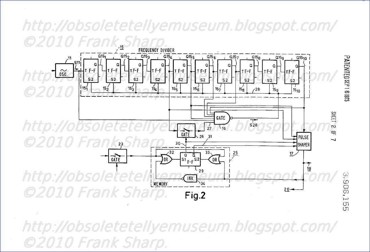 FIG. 2 shows in greater detail the parts 15, 16, 25 and 26 of the circuit arrangement according to the invention. In this embodiment, frequency divider circuit 15 consists of ten bistable elements, in this case flipflops 15 1 , 15 2 , . . . 15 10 which are formed in known manner and each of which divides by two. In order that divider circuit 15 is reset after the 625th period of the signal with the frequency 2f H to the initial position, i.e. the position at the commencement of the first period, the outputs of oscillator 11 and of flipflops 15 5 , 15 6 , 15 7 and 15 10 are connected to five inputs of the adjusting gate 16 formed as a NAND gate, while gate 26 is connected to a sixth input 27 thereof.
 FIG. 3 shows the operation of divider circuit 15 and adjusting gate 16 in which input 27 is initially left out of consideration, FIG. 3 shows the output signal S11 from oscillator 11 as well as the output signals Q15 1 , Q15 2 , . . . Q15 10 from flipflops 15 1 , 15 2 , . . . 15 10 and the signal S28 at the reset line 28 of the flipflops, which line connects the reset terminals (S 2 ) of all flipflops of divider circuit 15 and which is connected to the output of gate 16. The numbers T 1 , T 2 , . . . T 623 , T 624 , T 625 indicate the periods of signal S11, while H 1 , H 2 , . . . H 311 , H 312 indicate the corresponding line periods. For the raster commencing after period T 625 the notations T' 1 , T' 2 , . . . and H' 1 apply. Each flipflop reverses when a leading edge occurs in the output signal from the previous flipflop or from signal S11.
At the commencement of period T 1 , signals S11, Q15 1 , Q15 2 , . . . Q15 10 are "high" which may be indicated by the binary number 0. At the commencement of period T 2 , flipflop 15 1 reverses, signal Q15 1 becomes "low" which corresponds to the number 1. FIG. 3 shows that for the first six periods the flipflops indicate the following:
T 1 : 0000000000
t 2 : 0000000001
t 3 : 0000000010
t 4 : 0000000011
t 5 : 0000000100
and
T 6 : 0000000101
in which signals Q15 1 Q15 2 , . . . Q15 10 are written from the right to the left. These are the numbers 0, 1, 2, 3, 4 and 5 in the decimal system, that is to say, the number of the corresponding period reduced by 1. For the periods T 622 , T 623 , T 624 and T 625 the flipflops indicate the following:
T 622 : 1001101101
t 623 : 1001101110
t 624 : 1001101111
and
T 625 : 1001110000.
these are the numbers 621, 622, 623 and 624.
It is evident that gate 16 has received at least one 0 at one of its input up to the first half of period T 625 . FIG. 3 shows that during the second half of period T 625 signals S11, Q15 5 Q15 6 , Q15 7 and Q15 10 are simultaneously equal to 1 so that signal S28 becomes equal to 0. The pulse thus generated is applied as a reset pulse through line 28 to all flipflops of divider circuit 15. The flipflops which were not in the high state, i.e. flipflops 15 5 , 15 6 , 15 7 and 15 10 are brought to that state while the other flipflops do not change their state. At the commencement of the next period, period T' 1 , all flipflops indicate 0 and a new raster commences.
Memory element 25 includes a flipflop 29, an output 30 of which is connected to an input of gate 26 while another input of gate 26 is connected to the output of flipflop 15 4 . The outputs of an OR gate 32 and of an OR gate 33 are connected to the set (S 1 ) and the reset terminal (S 2 ), respectively, of flipflop 29. The output signal Q from flipflop 29 is present at output 30 and the other output signal Q is present at the other output 31 thereof. The output signals from switch 23 and pulse shaper 17 are applied to gate 33 while the output signals from switch 23 and an inverter stage 34 are applied to gate 32, while stage 34 reverses the output signal from pulse shaper 17 in its polarity.
 In the off-phase state, received pulses are passed by switch 23 (FIG. 4a) which do not coincide with the divider pulses (FIG. 4b) originating from pulse shaper 17. Consequently, gate 33 does not provide a signal (FIG. 4d). However, gate 32 receives the pulses of FIG. 4b and the pulses of FIG. 4c which are inverted relative thereto so that this gate is enabled. The first of the output pulses from gate 32 (FIG. 4e) sets flipflop 29 whose output signals consequently become Q = 1 and Q = 0. If flipflop 29 were already in this state, nothing would be changed.
When the on-phase state has been achieved after some time, one pulse from switch 23 (FIG. 5a) and one divider pulse (FIG. 5b) coincide for at least a part. Gate 33 is enabled (FIG. 5d) while gate 32 which receives the pulse of FIG. 5a and the pulse of FIG. 5c which is inverted relative to that of FIG. 5b does not provide a signal (FIG. 5e). Flipflop 29 is reset by the pulse of FIG. 5d, that is to say, the signals Q = 0 and Q = 1 are present at terminals 30 and 31, respectively. Gate 26 is a controlled switch and does not conduct under these circumstances. The operation of divider circuit 15 therefore remains the same as has been extensively described hereinbefore. If due to the inertia of integrator 21 other pulses might be passed by switch 23, the state will not change.
In the off-phase state for which Q = 1, gate 26 conducts so that the output signal Q15 4 from flipflop 15 4 is present at the input 27. FIG. 3 shows that Q15 4 = 0 during period T 625 . Signal S28 consequently remains equal to 1 and divider circuit 15 is not reset. FIG. 6 shows the further variation. This Figure shows that only during the second half of period T 633 , i.e. 8 periods later than in the
 on-phase state, the signals S11, Q15 4 , Q15 5 , Q15 6 , Q15 7 and Q15 10 applied to gate 16 are all equal to 1 so that a reset pulse S28 = 0 is generated. The next period is thus the first period T' i of a new raster.
The foregoing shows that memory element 25 ensures that, dependent on the fact whether the on-phase or off-phase state has occurred, the frequency divider circuit divides the frequency 2f H from signal S11 by the divisors 625 and 633 respectively. The following cases may occur:
1. on-phase state, with Q = 0 : the previous divisor was 625, Q remains 0, the on-phase state is maintained and neither the memory element nor the divider circuit are influenced;
2. on-phase state with Q = 1 : the previous divisor was 633, Q becomes 0 and the divisor becomes 625, which is the case as under 1;
3. off-phase state (longer than approximately 0.4 s) with Q = 0 : the previous divisor was 625, Q becomes 1 so that the divisor becomes 633; the pulses in FIGS. 5a and 5b have different repetition frequencies and are displaced relative to each other; after a given pull-in period, the on-phase state is reached which is the case as under 2;
4. off-phase state (longer than approximately 0.4 s) with Q = 1 : the previous divisor was 633 and remains so because Q remains equal to 1 which is the case as under 3.
The case under item 1 is thus always the final state in which neither any received signal nor any noise or interferences can reach the divider circuit. If the received field synchronising pulses drop out after this state has been reached the divider circuit continues to divide by 625 due to the action of the memory element so that the image displaced on the display screen of tube 6 remains in place. This is also the case with the known circuit arrangement which in fact has no other divisor than 625 but which, as already stated, is more sensitive to noise and interference with the attendant drawbacks. When the received signal is so weak that substantially no distinction can be made between interferences and field synchronising pulses or when these pulses drop out before the on-phase state is reached, the divisor 633 is used for division. The image "rolls over" in the vertical direction which is less disturbing to the observer and is less harmful for the screen than the brightly lit narrow images which can be displayed with the known circuit arrangement.
 FIG. 7 shows how the pull-in process is effected, i.e. when Q = 1. FIG. 7a shows the output pulses from pulse shaper 17 and FIG. 7b shows the pulses originating from trigger 24. Since the frequency of the latter pulses (=2f H /625) is higher than that of the former pulses (=2f H /633),
they are displaced relative thereto to the left until coincidence takes place in gates 32 and 33 : Q becomes 0; coincidence also takes place in the coincidence stage 20 and switch 23 is open. For each period of the frequency divider circuit the relative time difference Δ t between two received pulses 1 and 2 is equal to 8 times one period of signal S11, i.e. approximately 8 × 32 μs = 256 μs. One period of the frrquency divider circuit corresponds to 633 × 32/8 × 32 = 79 times Δ t. In the most unfavourable case in which the process commences with the pulse in the position 3 in FIG. 7b, this process will therefore take approximately 75 field periods, i.e. 1.5 s. In this extreme case, which is very improbable, it takes consequently approximately 0.4 + 1.5 = 1.9 s before the displayed image comes to a standstill.
It may occur that just before the end of the pull-in process the pulse of FIG. 7b occupies such a position, indicated by 4, that at the next position 5 after a period of time Δ t the leading edge of the pulse occurs just before the trailing edge of the pulse of FIG. 7a. As a result, the divider circuit is brought to the state with the divisor 625. Since the coincidence period is then very short, it is however evident that this situation is very sensitive to interference. This drawback is obviated according to an aspect of the invention in that the duration of the pulse in FIG. 7a is made longer at the instant when the 625-state occurs. Information therefor may be obtained from memory element 25 which thus fulfils a second function, which information is applied to pulse shaper 17.
FIG. 8 shows pulse shaper 17 in greater detail. The outputs of flipflop 15 4 and flipflop 15 5 are connected to the inputs of controlled switches 35 and 36, respectively. The switches 35 and 36 are controlled by the signals at the outputs 30 and 31, respectively, of memory element 25. The outputs of switches 35 and 36 are connected to two inputs of an adder stage 37. The output signal thereof is applied to a keyed gate 38 which is keyed by the output signal Q15 10 from flipflop 15 10 .
A pulse shaper is required in any case. The output signal Q15 10 from the frequency divider circuit has a natural frequency of 2f H /2 10 which corresponds to a natural period of approximately 33 ms. Circuit 15 is reset approximately 20 ms after the commencement of the period, i.e. 20 - 33/2 ≉ 3.5 ms after reversal in the middle of the natural period. Signal Q15 10 therefore has a flyback period of approcimately 3.5 ms and is thus not usable as a field control signal. According to the invention, the pulse shaper has also two states. In the state with divisor 633 of the divider circuit for which Q = 1 and Q = 0, switch 35 conducts while switch 36 is cut off. The output signal Q15 4 from flipflop 15 4 whose natural period is equal to 2 4 /2f h ≉ 512 μs is applied to gate 38. This gate is keyed in such a manner that only the first positive half period of signal Q15 4 is passed, that is to say, its output signal lasts until the first trailing edge. This may be obtained in known manner with the aid of bistable elements. This is the pulse in FIG. 7a, it lasts approximately 256 μs from the instant of resetting divider circuit 15. Since Δt ≉ 256 μs, this is exactly the duration which is at least required. As soon as the state with divisor 625 is achieved, there applies that Q = 0 and Q = 1. Switch 36 then conducts while switch 35 is cut off so that the output signal from gate 38 is the first positive half period of signal Q15 5 . This is the pulse in FIG. 7c and it lasts approximately 512 μs from the instant of resetting divider circuit 15. As a result, it is insured that the pulse in FIG. 7b in any case completely coincides therewith while the output signal from gate 38, hence from pulse shaper 17, is always suitable for controlling the field output stage 18. The flyback period thereof is in fact shorter than approximately 1 ms.
FIG. 7b shows that the largest possible time difference between the leading edges of the pulses is slightly shorter than approximately 256 μs, i.e. 0.256/20 ≉ 1.3 percent of a field period. This slight deviation is maintained as long as the occurred on-phase state lasts and produces a deviation in the vertical position of the image. It may be noted that this value, as well as the maximum duration of the pull-in process, emanates from the difference between the two divisors 633 and 625, i.e. 8 = 2 3 . A value different from 633 for the divider in the off-phase state may, however, be chosen. Instead of applying signal Q15 4 to adjusting gate 16, the supply of signal Q15 5 to this gate may be interrupted so that the divisor becomes 625 - 2 4 = 609. In this case, the time difference Δt in FIG. 7b lasts approximately 16 × 32 μs = 512 μs, so that the pull-in time has been reduced by 50 percent relative to the described case with a divisor of 633 while the minimum duration of the pulse in FIG. 7a must also be 512 μs. The extended pulse of FIG. 7c then lasts at least approximately 700 μs which is still just suitable as a field control signal. The largest possible vertical deviation is then, however, doubled.
Divisors other than 633 and 609 may be obtained by applying or not applying one or more output signals from the flipflops of divider circuit 15 to adjusting gate 16. For 633 the difference from the nominal divisor 625 is equal to +2 3 and for 609 it is -2 4 . The divisor 613, for example, corresponds to -2 4 +2 2 = -12 and may be realised by connecting for Q = 1 the output of flipflop 15 3 to an input of gate 16 and by interrupting the connection between the output of flipflop 15 5 and the relevant input of gate 16. Divisors other than 625 are obtained in that the connection between at least one of the flip-flops 15 5 , 15 6 , 15 7 , 15 10 to gate 16 is interrupted and/or in that at least one of the other flipflops is connected to gate 16. The considerations regarding divisor 609 have, however, shown that the choice of the second divisor cannot be limited in practice, while it is evident that in practice the second divisor should not deviate too much from the nominal divisor 625. Moreover, divisors 633 and 609 can be obtained in the easiest manner.
It is to be noted that it may occur that coincidence takes place in stage 20 but not in memory element 25 due to the shorter duration of the pulse generated by trigger 24. However, in such a case the divisor deviates from the value 625 so that the process described with reference to FIG. 7 is effected.
 FIG. 9 shows another embodiment of the circuit arrangement according to the invention in which a higher value than the nominal value 625, namely 633, is chosen for the divisor in the off-phase state. This embodiment is based on the following recognition. There are some test signal generators in which the number of lines per image is not 625 but, for example, 624, so that the displayed image is not interlaced. They are used, for example, for adjusting the convergence in colour television receivers. When using video recorders, it may occur that, for example, when displaying a stationary image, the number of line synchronising pulses per image slightly deviates from 625. Field synchronisation with the known circuit arrangement is impossible when such "non-standard signals" are received. The object of the embodiment of FIG. 9 is to establish synchronisation in such a case and for this purpose the direct synchronisation is used while the frequency divider circuit is set to the state with divisor 633. Since this state corresponds to a lower frequency than the nominal one, the direct synchronisation is possible while the drawbacks thereof do not in most cases apply because the received signal often comprises little noise and interferences.
The embodiment of FIG. 9 comprises parts which also occur in those of the previous Figures and which have the same reference numerals. In FIG. 9, 39 denotes a switch which may be, for example, manually operated and which is closed when the above-mentioned non-standard signals are received. As a result, the delay introduced by integrator 21 is reduced, for example, by making a time constant associated with this integrator shorter or by switching off integrator 21 completely. Coincidence stage 20 thus does not have any effect any longer. Also, the closure of switch 39 renders the input voltage of an amplifier 40 "high" so that its output voltage likewise becomes high (= 0). Under these circumstances, a controlled switch 41 which is connected to the output of trigger 24 starts to conduct so that the pulses originating from the trigger are passed and reach an input of an AND gate 42. Another input thereof is connected to the output of gate 16 and the output thereof is connected to the reset line 28 of the ten flipflops of divider circuit 15. The output voltage from amplifier 40 is also applied to an inverter stage 43 whose output voltage is low (= 1) when switch 39 is closed and is applied to an input of an OR gate 44. Another input of gate 44 is connected to the output of integrator 21 and its output is connected to the input of level detector 22. Furthermore, the output of inverter stage 43 is also connected to an extra input of OR gate 33.
Under the circumstances described, gates 44 and 33 do not provide any signal (= 1). The output signal from level detector 22 becomes 0 so that the controlled switch 23 conducts. Synchronising pulses originating from trigger 24 are passed on to OR gate 32. If they do not already have the values Q = 1 and Q = 0 the output signals from flipflop 29 consequently become Q = 1 and Q = 0. This is the state as described with reference to FIG. 6 for which frequency divider circuit 15 should be reset after the 633rd period of oscillator 11. In fact, the output signal from gate 16 then is 0 so that signal S28 is likewise 0. Before the 633rd period, however, a received field synchronising pulse is present through switch 41 at the relevant input of gate 42 (= 0) so that S28 = 0. Divider circuit 15 is thereby reset.
When standard signals are received (that is to say with 625 lines per image) switch 39 is open so that integrator 21 has the original time constant whilst switch 41 is cut off. Received field synchronising pulses can no longer reach gate 42. The output signal from inverter stage 43 is 0 so that those from OR gates 44 and 33 only depend on the signals from integrator 21 and switch 23, respectively. The circuit arrangement of FIG. 9 operates in the same way as those of FIGS. 1 and 2. It may be noted that the extension of the duration of the divider pulse after the occurrence of the on-phase state in case of reception of non-standard signals is not effected in the embodiment of FIG. 9 because signal Q remains equal to 1. This is no drawback because in the most cases little noise and interference are received.
The so-called negative logic is employed in the foregoing. It is evident that this choice is not important for the essence of the invention. For the positive logic only the denomination of the logical gates shown in the Fig. would have to be changed in known manner.
Elements 10 to 13, 15 to 17, 20 to 26 and 39 to 44 of the described circuit arrangements, with the exception of a capacitor possibly associated with integrator 21, may be advantageously integrated in a semi-conductor body. In view of the large number of components thereof, it is evident that a non-integrated embodiment would not be economical. It may be noted that the described frequency divider circuit and the memory element consist of binary elements. Embodiments of the same scope as described in the present patent application are, however, feasible, using elements of different types.
A television system employing 625 lines per image, two interlaced rasters per image and 50 fields per second has been taken as an example in the foregoing. It will be evident that modifications of the circuit arrangement according to the invention without an essential difference are possible for the reception of television signals in accordance with a different system.
Circuit arrangement for generating a control signal for the field output stage in a television receiver CHASSIS K11 (20AX) LINE CONTROL AND FRAME CONTROL UNITS
 A circuit arrangement for generating a control signal for the field output stage in a television receiver, provided with a frequency divider circuit by which the double line frequency is divided by a number equal to the number of lines per image. An automatic selection circuit insures that direct synchronization is used in the off-phase state and in case of reception of non-standard signals (for example, from video recorders).
A circuit arrangement for generating a control signal for the field output stage in a television receiver suitable for the reception of line and field synchronizing pulses, in which a plurality of fields constitutes an image
, said circuit arrangement comprising a generator for generating a signal of the line frequency or an integer multiple thereof, a field frequency generator coupled to said line frequency generator including a frequency divider circuit having an initial state, means for applying received field synchronizing pulses to a comparison stage for comparing the phase between these pulses and the pulses generated by the frequency divider circuit, the comparison stage applying a signal to a gate associated with said comparison stage, which signal is dependent on the phase difference between the compared pulses, the field generator having direct and indirect synchronization states, a gating pulse generator generating gating pulses, namely a first gating pulse during the occurrence of which the frequency divider circuit is reset to said initial state in the off-phase state of the compared pulses and a second gating pulse which is applied to an automatic selection circuit coupled to said field frequency generator, which selection circuit switches the field generator to the indirect synchronization state when a received field synchronizing pulse and a pulse generated by the frequency divider circuit at least partly occur simultaneously, and switches the field generator to the direct synchronization state when said pulses do not coincide during the occurrence of the second gating pulse. 2. A circuit arrangement as claimed in claim 1, wherein the gating pulses and the frequency divider pulses each have a repetition frequency, the repetition frequency of the gating pulses is equal to the repetition frequency of the pulses generated by the frequency divider circuit divided by an integer n and that each second gating pulse occurs a number of field periods after a first gating pulse. 3. A circuit arrangement as claimed in claim 2, wherein the pulse duration of the two gating pulses is at least approximately one field period. 4. A circuit arrangement as claimed in claim 1, wherein the automatic selection circuit includes a gating device and a bistable element, the field synchronizing pulses, the pulses generated by the frequency divider circuit and the second gating pulses being applied to said gating device, the output signal from the gating device being applied to the bistable element an output signal of which is a second input signal for the gate associated with the comparison stage. 5. A circuit arrangement as claimed in claim 4, wherein said bistable element has a state corresponding to direct synchronization and further comprising a second gating device receiving field synchronizing pulses through a controlled switch rendered conducting by the gate associated with the comparison stage during the off-phase state of the compared pulses, the output signal from the second gating device resetting the frequency divider circuit during the occurrence of the first gating pulse and bringing the bistable element into the state corresponding to the direct synchronization. 6. A circuit arrangement as claimed in claim 1, further comprising a free-running oscillator which is synchronized by the pulses originating from the frequency divider circuit in case of indirect synchronization and by the received field synchronizing pulses in case of direct synchronization. 7. A circuit arrangement as claimed in claim 1, wherein at least the frequency divider circuit, the gating pulse generator, the automatic selection circuit and the gating devices are integrated in a semiconductor body. 8. A circuit arrangement as claimed in claim 2, wherein the gating pulse generator includes an auxiliary frequency divider circuit for dividing the repetition frequency of the pulses generated by the frequency divider circuit. 9. A circuit arrangement as claimed in claim 8, wherein the integer n is determined by the condition ##EQU2## wherein N is the number of lines per image in the television system for which the television receiver is suitable and d is chosen as a function of the number of lines per image of the received television signal. 10. A circuit arrangement for generating a control signal for the field output stage in a television receiver suitable for the reception of line and field synchronizing pulses, in which a plurality of fields constitutes an image, said circuit comprising a generator means for generating a signal of the line frequency or an integer multiple thereof, a field frequency generator circuit coupled to said line frequency generator and having direct and indirect synchronization states and including a frequency divider circuit having an initial state, a comparison stage means coupled to said divider, means for applying received field synchronizing pulses to said comparison stage means for comparing the phase between these pulses and the pulses generated by the frequency divider circuit, a gate, the comparison stage means comprising means for applying a signal to said gate which signal is dependent on the phase difference between the compared pulses, an automatic selection circuit coupled to said gate, a gating pulse generator means coupled to said selection circuit for generating gating pulses, said pulses comprising a first gating pulse during the occurrence of which the frequency divider circuit is reset to said initial state in the off-phase state of the compared pulses and a second gating pulse which is applied to said automatic selection circuit which selection circuit switches the field generator circuit to indirect synchronization when a received field synchronizing pulse and a pulse generated by the frequency divider circuit at least partly occur simultaneously, and switches the field generator circuit to direct synchronization when said pulses do not coincide during the occurrence of the second gating pulse. Description:
The invention relates to a circuit arrangement for generating a control signal for the field output stage in a television receiver suitable for the reception of line and field synchronizing pulses, in which a number of fields constitutes an image, provided with a generator for generating a signal of the line frequency of an integer multiple thereof, a frequency divider circuit and means for applying received field synchronizing pulses to a comparison stage for comparing the phase between these pulses and the pulses generated by the frequency divider circuit, the comparison stage being capable of applying a signal to a gate which signal is dependent on the phase difference between the compared pulses, the circuit arrangement being switchable between direct and indirect synchronization.
Such a circuit arrangement is described in U.S. Pat. No. 3,708,621. Since in this known circuit arrangement the control signal is derived from the line synchronizing signal by means of frequency division, the frequency thereof is correct as soon as the line synchronizing circuit has synchronized in frequency with respect to the received line synchronization signal, which is generally effected fairly quickly. The correct phase of the field control signal obtained relative to the field synchronizing pulses originating from the transmitter and received by the television receiver is insured by the comparison stage which may be formed as a coincidence gate, and an integrator. In the off-phase state the comparison stage provides a plurality of pulses so that the integrator supplies a signal after a given period which enables the gate. The frequency divider circuit is then reset: this is direct synchronization in which the generated control signal is directly influenced by the received synchronizing pulses. The phase is then correct, the comparison stage no longer provides any pulse and the received synchronizing pulses can in principle no longer reach the divider circuit, at least not as long as the signal generated by the circuit arrangement maintains the same frequency and same phase as the received pulses: this is indirect synchronization in which the received synchronizing pulses cannot directly influence the generated control signal.
It is an object of the invention to provide a circuit arrangement which is also suitable for the reception of "non-standard signals" which are signals in which the number of lines per image deviates from the number prescribed in the relevant television syste m. Such signals are generated by some test signal generators in which the displayed image is not interlaced and which are used, for example, for adjusting the convergence in colour television receivers or may be produced when using video recorders, for example, for the display of still pictures. Field synchronization with the known circuit arrangement is impossible when such signals are received, for the frequency of the received field synchronizing pulses deviates from the frequency of the pulses obtained by division so that a vertical roll-over is obtained. Some received synchronizing pulses reset, however, the frequency divider circuit so that the image occasionally jumps in the vertical direction.
The circuit arrangement according to the invention is characterized in that it further comprises a gating pulse generator generating gating pulses, namely a first gating pulse during the occurrence of which the frequency divider circuit is reset in the off-phase state of the compared pulses and a second gating pulse which is applied to an automatic selection circuit which selection circuit switches the circuit arrangement to indirect synchronization when a received field synchronizing pulse and a pulse generated by the frequency divider circuit at least partly coincide, and switches the circuit arrangement to direct synchronization when said pulses do not coincide during the occurrence of the second gating pulse.
The invention will be described in greater detail by way of example with reference to the accompanying Figures in which
FIG. 1 shows a block-schematic diagram of a television receiver provided with the circuit arrangement according to the invention,
FIG. 2 shows details of the circuit arrangement according to the invention,
FIGS. 3, 4 and 5 show waveforms which occur in the circuit arrangement according to the invention.
I n FIG. 1, 1 is an aerial by which a television signal can be received. This signal is applied to an RF and detection section 2. The detected signal subsequently reaches the audio section 3 of the television receiver and a video amplifier 4 at the output of which a complete video signal, possibly with a chrominance signal in the case of colour television is available. This signal is applied to a section 5 in which it is processed whereafter a picture display tube 6 is controlled, and to a sync. separator 7. The output voltage thereof includes line synchronizing pulses which are applied to a phase detector 8 whose output voltage can influence an oscillator 11 through a flywheel filter 9 and a reactance circuit 10. Oscillator 11 generates a voltage of the double line frequency 2f H , i.e., 31250 Hz upon reception of a signal in accordance with the television system using 625 lines per complete image, 2 interlaced fields per image and 50 fields per second. Another possibility is that oscillator 11 generates a voltage of the line frequency f H whose frequency is subsequently doubled. The voltage of the frequency 2f H controls a frequency divider circuit 12 in which its frequency is divided by two and the signal thus obtained is applied through a pulse shaper 13 to the line output stage 14 which provides the line deflection current for the deflection coil (not shown) for the horizontal deflection of the electron beam(s) in tube 6.
The voltage available at the output of oscillator 11 is also applied to a generator 15 of field frequency signals in which its frequency is divided by the divisor 625 and is further processed. When oscillator 11 has the correct frequency after in frequency synchronization of the circuit 8, 9, 10, 11 for the indirect line synchronization, the frequency of the signal generated by generator 15 is also correct, that is to say, it is equal to the field frequency at the mentioned standard of 50 Hz. A pulse shaper 17 receives the signal generated by generator 15 and controls the field output stage 18 which applies the field deflection current to the deflection coil (not shown) for the vertical deflection of the electron beam(s) in tube 6. Both the line and the field control signals have the waveform required for stages 14 and 18 due to the two pulse shapers 13 and 17, respectively. If the output signal of divider circuit 12 or generator 15 has already this shape, pulse shapers 13 and 17, respectively, may be omitted.
The output voltage of sync. separator 7 also includes field synchronizing pulses which are separately obtained by means of a field sync. separator 19 and are subsequently applied to an input of a coincidence gate 20. The divider pulses originating from an output of generator 15 are present at a second input of gate 20. In the on-phase state that is to say, in the case where a field synchronizing pulse originating from separator 19 and a divider pulse coincide at least partly, stage 20 does not provide a signal. In the off-phase state it provides a signal namely the divider pulse for an integrator 21 which is followed by a level detector 22. When this state lasts at least approximately 0.4 s which corresponds to approximately 20 pulses, the detected level exceeds a given threshold value so that a signal is applied to an input of an AND gate 16. The field synchronizing pulses at the output of separator 19 reach an input of an OR-gate 25 through a controlled switch 23 which can be rendered conducting by the output signal from gate 16. The same output signal is also applied to generator 15.
A further input of gate 16 is connected to an output of an automatic selection circuit 26 while the output signal from gate 25 is applied in a manner to be described hereinafter to generator 15 and to circuit 26. The output signal from pulse shaper 17 is applied to a pulse generator 27 having two outputs one of which is connected to an input of gate 25 and one is connected to an input of circuit 26. The divider pulses which are applied to coincidence stage 20 are also applied to an input of selection circuit 26 while another input thereof as well as another input of generator 15 receive the pulses originating from separator 19.
 A control signal for the field output stage is generated by generator 15 with the aid of pulse generator 27 and selection circuit 26. This control signal always has the correct frequency and the correct phase after a short pull-in period irrespective of whether the field synchronizing pulses received from separator 19 are standard signals or not. This will be explained with reference to FIG. 2 in which elements 15, 26 and 27 of FIG. 1 are shown in greater detail.
Generator 15 includes a frequency divider circuit 29 which in known manner, for example, by means of bistable elements, divides the frequency 2f H of the signal generated by oscillator 11 by 625. As is known ten bistable elements must be present so that the output signal from circuit 29 has a natural frequency of (2f H /2 10 ) which corresponds to a natural period of approximately 33ms. Circuit 29 is internally reset after a field period i.e., approximately 20 ms after the commencement of the period, i.e., 20 - 33/2 ≉ 3.5 ms after reversal in the middle of the natural period. A pulse shaper 30 reduces this flyback pulse to approximately 300 μs which is slightly longer than the field synchronizing pulse provided by separator 19 and whose duration is approximately 200 μs. These pulses are compared in coincidence stage 20. The output signal from pulse shaper 30 also reaches through a first controlled switch 31 a NOR-gate 32. A further input of gate 32 receives through a second controlled switch 33 the output signal from separator 19. The output signal from gate 32 serves as a trigger signal for an oscillator 34 formed in known manner which provides the output signal of generator 15. Switch 33 can be rendered conducting by the output signal from gate 16 while the same signal can render switch 31 conducting through an inverter stage 35. Finally the reset terminal (S 2 ) of divider circuit 29 is connected to the output of gate 25.
Pulse generator 27 includes an auxiliary frequency divider circuit 36 which may be a counter and by which the repetition frequency in this example 50 Hz of its input signal (FIG. 3a) is divided by an integer n. In this example n is equal to 16, so that the output signal from circuit 36 has a period of n × 20 = 16 × 20 = 320 ms and has the shape as is shown in FIG. 3b. This signal is applied to a gating pulse shaper 37 which generates in known manner two series of gating pulses of the same repetition frequency as that of the signal in FIG. 3b. The first gating pulse (FIG. 3c) is applied to gate 25 and has a duration of approximately 20 ms, that is to say approximately one field period. It is generated for example by a monostable element which is responsive to a trailing edge of the signal in FIG. 3b. The second gating pulse (FIG. 3d) has approximately the same duration as the first and occurs a given number of field periods later, in this example n - 1 = 15, so that its final edge coincides with the leading edge of the next first gating pulse. The second gating pulse is applied to an input of an OR gate 38 forming part of the automatic selection circuit 26. In FIG. 3a the field frequency pulses are shown to be very narrow. In practice they have a given duration so that every time one of these pulses coincides with one of the pulses of FIG. 3c and FIG. 3d. The pulses of FIG. 3c and 3d may alternatively be shifted in such a manner that they commence and end in the period located between two pulses of FIG. 3a.
The divider pulses from pulse shaper 30 and the synchronizing pulses from separator 19 are applied to other inputs of gate 38. The outputs of gate 38 and of gate 25 are connected to the set (S 1 ) and reset terminals (S 2 ), respectively, of a flipflop 39 whose Q-output is connected to an output of gate 16.
Oscillator 34 is a free-running oscillator, for example an astable multivibrator, which receives trigger pulses through a gate 32. FIG. 2 shows that these pulses originate from either separator 19 (direct synchronization), or from frequency divider circuit 29 (indirect synchronization), which will now be described in greater detail.
In the on-phase state level detector 22 does not apply a signal to gate 16 which may be indicated by the binary digit 1. During the period of the second gate pulse all input signals from gate 38 coincide at least partly which corresponds to the digit 0 for each input. Under these circumstances the output signal from gate 38 is also 0, that is to say, a set pulse is applied to terminal S 1 of flipflop 39 so that the output signal Q thereof is 1. The output signal from gate 16 is therefore 1 with the result that switches 23 and 33 are cut off when switch 31 is conducting. The divider pulses are applied through gate 32 to oscillator 34. One of the inputs of gate 25 conveys the signal 1, the output signal thereof is consequently 1: neither divider circuit 29 nor flipflop 39 can be reset. As long as the on-phase state prevails, which means that coincidence occurs every second gating pulse at gate 38 and that level detector 22 provides the signal 1, the situation shown is maintained while the generated control signal cannot be influenced by the received synchronizing pulses.
When the off-phase state occurs, level detector 22 provides after approximately 0.4 s a signal which is equal to 0 for gate 16. The output signal thereof becomes 0 so that switches 23 and 33 conduct while switch 31 is cut off. The synchronizing pulses received from separator 19 are applied through gate 32 to oscillator 34 while the divider pulses cannot influence this oscillator (direct synchronization). The generated control signal is then synchronous with the received signal, but as is shown the duration of this state must be short due to the higher sensitivity to interference of the circuit at least when receiving broadcasting television signals. This is effected as follows. Since the first gating pulse from generator 27 takes approximately one field period a synchronizing pulse occurs fairly quickly simultaneously with a first gating pulse. Both inputs of gate 25 are therefore equal to 0 so that the output thereof is also 0. Frequency divider circuit 29 is reset. Since there is no coincidence in gate 38 the output signal thereof is equal to 1. This is the signal at the terminal S 1 of flipflop 39 while terminal S 2 receives a 0. Flipflop 39 is thus reset: Q becomes 0, but circuit 26 has no influence on the rest of the circuit because level detector 22 provides a signal which is equal to 0 for gate 16.
When the incoming signals are standard signals, the above-described situation remains while the divider pulses and the synchronizing pulses are always in phase, this until the occurrence of the next second gating pulse from pulse generator 27. During this occurrence the three input signals of gate 38 are equal to 0 so that a reset pulse 0 is applied to the terminal S 1 of flipflop 39: Q becomes 1. The input signals from coincidence stage 20 coincide since the beginning of the direct synchronization so that both input signals of gate 16 become equal to 1 at the instant when Q = 1. The output signal from gate 16 thus becomes 1 so that switches 23 and 33 are cut off and switch 31 conducts. Consequently the received signal does not reach the oscillator 34 while the divider pulses are applied to this oscillator (indirect synchronization). Nothing is changed in the state of divider circuit 29 because the output signal of switch 23 and consequently that of gate 25 becomes equal to 1 so that circuit 29 and flipflop 39 are not reset.
After the second gating pulse the output signal from gate 38 becomes equal to 0, but this does not change the state of flipflop 39. During the next second gating pulse a set pulse is applied to flipflop 39 but the output signal Q thereof was already 1 and thus does not change. The foregoing shows that the time elapsing until indirect synchronization occurs is as long as the time interval between both gating pulses, i.e., in the described example (n-1) × 20 = 15 × 20 = 300 ms after the off-phase state is established, i.e., approximately 0.4 s after its occurrence, increased by the time which is necessary for coincidence of a synchronizing pulse with a first gating pulse. Since the divisor corresponding to the incoming synchronizing pulses will not deviate in practice very much from 625 the latter period will last not more than a period of the first gating pulse, i.e., 320 ms. This is the reason why both gating pulses have a duration of approximately one field period. When this duration is shorter it is possible that no coincidence is effected even when receiving standard signals so that the circuit never pulls in. On the other hand a too long duration might render the circuit more sensitive to interference. FIG. 3 shows that a duration of approximately one field period can simply be realized.
When the incoming signals are not standard signals the circuit behaves in a different manner. Since divider circuit 29 is reset during the occurrence of the first gating pulse the two input signals from coincidence stage 20 coincide at least once. It is however uncertain whether this happens more than once and what is the output signal from level detector 22. This, however, has no influence on the manner of synchronization: in fact the divider pulse and the synchronizing pulse do not occur simultaneously during the occurrence of the second gating pulse so that the output signal Q from flipflop 39 remains equal to 0 and hence those of gates 16 and 25 also remain 0 independent of the situation in stage 20. As long as non-standard signals are received the synchronization of oscillator 34 thus remains direct which is no drawback because the signal generated by test signal generators and video recorders generally includes little noise and interference.
Divider circuit 29 is reset at each first gating pulse. When the incoming signal is a standard signal, the divider pulses and the synchronizing pulses are in phase. At the next second gating pulse coincidence is effected in gate 38 so that the circuit is immediately switched over to indirect synchronization. Otherwise a new cycle of n field periods will start. Another function of resetting divider switch 29 every time is the following. When receiving nonstandard signal the time difference between the divider and the synchronizing pulse would increase without this step, with the risk that coincidence might take place in gate 38 at an arbitrary instant so that an unwanted indirect synchronization might be the result.
After the divider pulse and the synchronizing pulse have coincided during the occurrence of the first gating pulse a time difference increasing each period is produced between these pulses upon reception of non-standard signals. Since the period of the signal generated by oscillator 11 is 1/2f H ≉ 32 μs, this difference after one field period is equal in μs to 32 × (625 - d) in which d is the divisor of the incoming signal deviating from 625. The number n must be chosen to be such that the time difference (n-1) × 32 × (625-d) can be observed by gate 38 after n-1 periods. FIG. 4a shows a synchronizing pulse and FIG. 4b shows a divider pulse which pulses have the stated duration of approximately 200 μs and in an extreme case of the on-phase state this is the state at which the two leading edges coincide. FIG. 4c shows the extreme case of the off-phase state which might occur subsequently and which is the state at which the leading edge of the synchronizing pulse coincides with the trailing edge of the divider pulse. FIG. 5a, 5b and 5c show the opposite situation. FIG. 4a, 4b, 4c, and 5a, 5b and 5c show that the above-mentioned time difference must be in the order of 300 μs. The number n is thus determined by the condition ##EQU1## which proves that the more the divisor d deviates from 625 the less n may be. When for the sake of security the smallest possible difference 625-d = ± 1 is chosen, i.e., d is 624 or 626, a value is found for n which is at least equal to 11. Auxiliary frequency divider circuit 36 might in principle divide the field frequency by 11, but it is simpler to divide by 16, for example, by means of four binary elements, for example, flipflops. As a result the pull-in time is slightly extended relative to the case where n = 11, namely 300 ms instead of 10 × 20 = 200 ms, but it is still acceptable while also the reliability and the insensitivity to interference are increased.
The foregoing shows that the output signal Q from automatic selection circuit 26 is equal to 0 in the off-phase state and becomes 1 after some time when standard signals are received so that synchronization is firstly effected directly and then indirectly. When receiving nonstandard signals Q remains equal to 0 so that direct synchronization is maintained.
It will be noted that the gating pulses in FIGS. 3c and 3d succeed each other after n-1 field periods so that the final edge of one pulse coincide with the leading edge of the other. It will be evident that this is not of essential importance, that is to say, a given time may elapse between these edges. Neither is it necessary for auxiliary frequency divider circuit 36 to divide the frequency of the signal from pulse shaper 17 and not, for example, that from oscillator 34 or from divider circuit 29. Oscillator 34 may be omitted in the case where the output signal from gate 32 has the correct waveform to control pulse shaper 17. In the embodiment of FIG. 2 the gating pulses are obtained by means of auxiliary frequency divider circuit 36. A different method is alternatively possible, namely the integration of the pulses of FIG. 3a. By means of suitable pulse shapers gating pulses can then be obtained whose repetition frequency is not necessarily equal to the field frequency divided by an integer such as is the case with circuit 36.
The so-called negative logic is used in the foregoing, that is to say, the logic in which 0 means "signal" and 1 means "not signal." It is obvious that this choice is not important for the essence of the invention. With the positive logic only the terms for the logical gates shown in FIGS. 1 and 2 would have to be changed in known manner.
Elements 10 to 13, 15 to 17 and 20 to 27 of the described circuit, except for a capacitor optionally associated with integrator 21 may advantageously be integrated in a semiconductor body. In view of the large number of components thereof it is obvious that a non-integrated embodiment would not be economical. It may be noted that the described embodiment includes binary elements. Embodiments of the same scope as in the present application are, however, feasible in which different elements may be used.
A television system using 625 lines per image, 2 interlaced fields per image and 50 fields per second has been used hereinbefore as an example. It will be evident that modifications of the circuit according to the invention are possible without essential difference for the reception of television signals in accordance with a different system.
PHILIPS PAL CHROMA DELAY LINE:
An improved ultrasonic delay line comprising a solid glass body having one or more slits in the side walls extending inwardly from the outer edge faces of the body. The slits are arranged in the path of the propagating ultrasonic energy so as to effectively increase the number of energy transmission paths in the body by acting as additional energy reflecting surfaces. The slits extend the effective length of the delay line. The slits also operate to reduce undesired cross-coupling between the input and output transducers.
GLASS TECHNOLOGY FOR PHILIPS PAL CHROMA DELAY LINE / ACOUSTIC DELAY LINE:
A glass for an acoustic delay line which consists of SiO2, Al2 O3, B2 O3 and an oxide of a bivalent metal and satisfies the requirement that -5×10⁻⁶ <Σi αi x1 < +5×10⁻⁶ where αi is the temperature coefficient of the rate of propagation in the range of 20°-70° C for the oxide component i and xi is the molar fraction of that component.
1. In an acoustic delay line of the type having signal converting elements on the surface of a glass body for converting an input electric signal into an acoustic signal and an output acoustic signal into an electrical signal, the improvement comprising that said body of glass consist of the following compositions in wt. percent: 2. In an acoustic delay line of the type having signal converting elements on the surface of a glass body for converting an input electric signal into an acoustic signal and an output acoustic signal into an electric signal, the improvement comprising that said body of glass consist of the following composition in wt. percent:
Such a circuit arrangement is described in U.S. Pat. No. 3,708,621. Since in this known circuit arrangement the control signal is derived from the line synchronizing signal by means of frequency division, the frequency thereof is correct as soon as the line synchronizing circuit has synchronized in frequency with respect to the received line synchronization signal, which is generally effected fairly quickly. The correct phase of the field control signal obtained relative to the field synchronizing pulses originating from the transmitter and received by the television receiver is insured by the comparison stage which may be formed as a coincidence gate, and an integrator. In the off-phase state the comparison stage provides a plurality of pulses so that the integrator supplies a signal after a given period which enables the gate. The frequency divider circuit is then reset: this is direct synchronization in which the generated control signal is directly influenced by the received synchronizing pulses. The phase is then correct, the comparison stage no longer provides any pulse and the received synchronizing pulses can in principle no longer reach the divider circuit, at least not as long as the signal generated by the circuit arrangement maintains the same frequency and same phase as the received pulses: this is indirect synchronization in which the received synchronizing pulses cannot directly influence the generated control signal.
It is an object of the invention to provide a circuit arrangement which is also suitable for the reception of "non-standard signals" which are signals in which the number of lines per image deviates from the number prescribed in the relevant television syste
m. Such signals are generated by some test signal generators in which the displayed image is not interlaced and which are used, for example, for adjusting the convergence in colour television receivers or may be produced when using video recorders, for example, for the display of still pictures. Field synchronization with the known circuit arrangement is impossible when such signals are received, for the frequency of the received field synchronizing pulses deviates from the frequency of the pulses obtained by division so that a vertical roll-over is obtained. Some received synchronizing pulses reset, however, the frequency divider circuit so that the image occasionally jumps in the vertical direction.The circuit arrangement according to the invention is characterized in that it further comprises a gating pulse generator generating gating pulses, namely a first gating pulse during the occurrence of which the frequency divider circuit is reset in the off-phase state of the compared pulses and a second gating pulse which is applied to an automatic selection circuit which selection circuit switches the circuit arrangement to indirect synchronization when a received field synchronizing pulse and a pulse generated by the frequency divider circuit at least partly coincide, and switches the circuit arrangement to direct synchronization when said pulses do not coincide during the occurrence of the second gating pulse.
The invention will be described in greater detail by way of example with reference to the accompanying Figures in which
FIG. 1 shows a block-schematic diagram of a television receiver provided with the circuit arrangement according to the invention,
FIG. 2 shows details of the circuit arrangement according to the invention,
FIGS. 3, 4 and 5 show waveforms which occur in the circuit arrangement according to the invention.
I
n FIG. 1, 1 is an aerial by which a television signal can be received. This signal is applied to an RF and detection section 2. The detected signal subsequently reaches the audio section 3 of the television receiver and a video amplifier 4 at the output of which a complete video signal, possibly with a chrominance signal in the case of colour television is available. This signal is applied to a section 5 in which it is processed whereafter a picture display tube 6 is controlled, and to a sync. separator 7. The output voltage thereof includes line synchronizing pulses which are applied to a phase detector 8 whose output voltage can influence an oscillator 11 through a flywheel filter 9 and a reactance circuit 10. Oscillator 11 generates a voltage of the double line frequency 2f H , i.e., 31250 Hz upon reception of a signal in accordance with the television system using 625 lines per complete image, 2 interlaced fields per image and 50 fields per second. Another possibility is that oscillator 11 generates a voltage of the line frequency f H whose frequency is subsequently doubled. The voltage of the frequency 2f H controls a frequency divider circuit 12 in which its frequency is divided by two and the signal thus obtained is applied through a pulse shaper 13 to the line output stage 14 which provides the line deflection current for the deflection coil (not shown) for the horizontal deflection of the electron beam(s) in tube 6.The voltage available at the output of oscillator 11 is also applied to a generator 15 of field frequency signals in which its frequency is divided by the divisor 625 and is further processed. When oscillator 11 has the correct frequency after in frequency synchronization of the circuit 8, 9, 10, 11 for the
indirect line synchronization, the frequency of the signal generated by generator 15 is also correct, that is to say, it is equal to the field frequency at the mentioned standard of 50 Hz. A pulse shaper 17 receives the signal generated by generator 15 and controls the field output stage 18 which applies the field deflection current to the deflection coil (not shown) for the vertical deflection of the electron beam(s) in tube 6. Both the line and the field control signals have the waveform required for stages 14 and 18 due to the two pulse shapers 13 and 17, respectively. If the output signal of divider circuit 12 or generator 15 has already this shape, pulse shapers 13 and 17, respectively, may be omitted.The output voltage of sync. separator 7 also includes field synchronizing pulses which are separately obtained by means of a field sync. separator 19 and are subsequently applied to an input of a coincidence gate 20. The divider pulses originating from an output of generator 15 are present at a second input of gate 20. In the on-phase state that is to say, in the case where a field synchronizing pulse originating from separator 19 and a divider pulse coincide at least partly, stage 20 does not provide a signal. In the off-phase state it provides a signal namely the divider pulse for an integrator 21 which is followed by a level detector 22. When this state lasts at least approximately 0.4 s which corresponds to approximately 20 pulses, the detected level exceeds a given threshold value so that a signal is applied to an input of an AND gate 16. The field synchronizing pulses at the output of separator 19 reach an input of an OR-gate 25 through a controlled switch 23 which can be rendered conducting by the output signal from gate 16. The same output signal is also applied to generator 15.
A further input of gate 16 is connected to an output of an automatic selection circuit 26 while the output signal from gate 25 is applied in a manner to be described hereinafter to generator 15 and to circuit 26. The output signal from pulse shaper 17 is applied to a pulse generator 27 having two outputs one of which is connected to an input of gate 25 and one is connected to an input of circuit 26. The divider pulses which are applied to coincidence stage 20 are also applied to an input of selection circuit 26 while another input thereof as well as another input of generator 15 receive the pulses originating from separator 19.
 A control signal for the field output stage is generated by generator 15 with the aid of pulse generator 27 and selection circuit 26. This control signal always has the correct frequency and the correct phase after a short pull-in period irrespective of whether the field synchronizing pulses received from separator 19 are standard signals or not. This will be explained with reference to FIG. 2 in which elements 15, 26 and 27 of FIG. 1 are shown in greater detail.
Generator 15 includes a frequency divider circuit 29 which in known manner, for example, by means of bistable elements, divides the frequency 2f H of the signal generated by oscillator 11 by 625. As is known ten bistable elements must be present so that the output signal from circuit 29 has a natural frequency of (2f H /2 10 ) which corresponds to a natural period of approximately 33ms. Circuit 29 is internally reset after a field period i.e., approximately 20 ms after the commencement of the period, i.e., 20 - 33/2 ≉ 3.5 ms after reversal in the middle of the natural period. A pulse shaper 30 reduces this flyback pulse to approximately 300 μs which is slightly longer than the field synchronizing pulse provided by separator 19 and whose duration is approximately 200 μs. These pulses are compared in coincidence stage 20. The output signal from pulse shaper 30 also reaches through a first controlled switch 31 a NOR-gate 32. A further input of gate 32 receives through a second controlled switch 33 the output signal from separator 19. The output signal from gate 32 serves as a trigger signal for an oscillator 34 formed in known manner which provides the output signal of generator 15. Switch 33 can be rendered conducting by the output signal from gate 16 while the same signal can render switch 31 conducting through an inverter stage 35. Finally the reset terminal (S 2 ) of divider circuit 29 is connected to the output of gate 25.
Pulse generator 27 includes an auxiliary frequency divider circuit 36 which may be a counter and by which the repetition frequency in this example 50 Hz of its input signal (FIG. 3a) is divided by an integer n. In this example n is equal to 16, so that the output signal from circuit 36 has a period of n × 20 = 16 × 20 = 320 ms and has the shape as is shown in FIG. 3b. This signal is applied to a
 gating pulse shaper 37 which generates in known manner two series of gating pulses of the same repetition frequency as that of the signal in FIG. 3b. The first gating pulse (FIG. 3c) is applied to gate 25 and has a duration of approximately 20 ms, that is to say approximately one field period. It is generated for example by a monostable element which is responsive to a trailing edge of the signal in FIG. 3b. The second gating pulse (FIG. 3d) has approximately the same duration as the first and occurs a given number of field periods later, in this example n - 1 = 15, so that its final edge coincides with the leading edge of the next first gating pulse. The second gating pulse is applied to an input of an OR gate 38 forming part of the automatic selection circuit 26. In FIG. 3a the field frequency pulses are shown to be very narrow. In practice they have a given duration so that every time one of these pulses coincides with one of the pulses of FIG. 3c and FIG. 3d. The pulses of FIG. 3c and 3d may alternatively be shifted in such a manner that they commence and end in the period located between two pulses of FIG. 3a.
The divider pulses from pulse shaper 30 and the synchronizing pulses from separator 19 are applied to other inputs of gate 38. The outputs of gate 38 and of gate 25 are connected to the set (S 1 ) and reset terminals (S 2 ), respectively, of a flipflop 39 whose Q-output is connected to an output of gate 16.
Oscillator 34 is a free-running oscillator, for example an astable multivibrator, which receives trigger pulses through a gate 32. FIG. 2 shows that these pulses originate from either separator 19 (direct synchronization), or from frequency divider circuit 29 (indirect synchronization), which will now be described in greater detail.
In the on-phase state level detector 22 does not apply a signal to gate 16 which may be indicated by the binary digit 1. During the period of the second gate pulse all input signals from gate 38 coincide at least partly which corresponds to the digit 0 for each input. Under these circumstances the output signal from gate 38 is also 0, that is to say, a set pulse is applied to terminal S 1 of flipflop 39 so that the output signal Q thereof is 1. The output signal from gate 16 is therefore 1 with the result that switches 23 and 33 are cut off when switch 31 is conducting. The divider pulses are applied through gate 32 to oscillator 34. One of the inputs of gate 25 conveys the signal 1, the output signal thereof is consequently 1: neither divider circuit 29 nor flipflop 39 can be reset. As long as the on-phase state prevails, which means that coincidence occurs every second gating pulse at gate 38 and that level detector 22 provides the signal 1, the situation shown is maintained while the generated control signal cannot be influenced by the received synchronizing pulses.
When the off-phase state occurs, level detector 22 provides after approximately 0.4 s a signal which is equal to 0 for gate 16. The output signal thereof becomes 0 so that switches 23 and 33 conduct while switch 31 is cut off. The synchronizing pulses received from separator 19 are applied through gate 32 to oscillator 34 while the divider pulses cannot influence this oscillator (direct synchronization). The generated control signal is then synchronous with the received signal, but as is shown the duration of this state must be short due to the higher sensitivity to interference of the circuit at least when receiving broadcasting television signals. This is effected as follows. Since the first gating pulse from generator 27 takes approximately one field period a synchronizing pulse occurs fairly quickly simultaneously with a first gating pulse. Both inputs of gate 25 are therefore equal to 0 so that the output thereof is also 0. Frequency divider circuit 29 is reset. Since there is no coincidence in gate 38 the output signal thereof is equal to 1. This is the signal at the terminal S 1 of flipflop 39 while terminal S 2 receives a 0. Flipflop 39 is thus reset: Q becomes 0, but circuit 26 has no influence on the rest of the circuit because level detector 22 provides a signal which is equal to 0 for gate 16.
When the incoming signals are standard signals, the above-described situation remains while the divider pulses and the synchronizing pulses are always in phase, this until the occurrence of the next second gating pulse from pulse generator 27. During this occurrence the three input signals of gate 38 are equal to 0 so that a reset pulse 0 is applied to the terminal S 1 of flipflop 39: Q becomes 1. The input signals from coincidence stage 20 coincide since the beginning of the direct synchronization so that both input signals of gate 16 become equal to 1 at the instant when Q = 1. The output signal from gate 16 thus becomes 1 so that switches 23 and 33 are cut off and switch 31 conducts. Consequently the received signal does not reach the oscillator 34 while the divider pulses are applied to this oscillator (indirect synchronization). Nothing is changed in the state of divider circuit 29 because the output signal of switch 23 and consequently that of gate 25 becomes equal to 1 so that circuit 29 and flipflop 39 are not reset.
After the second gating pulse the output signal from gate 38 becomes equal to 0, but this does not change the state of flipflop 39. During the next second gating pulse a set pulse is applied to flipflop 39 but the output signal Q thereof was already 1 and thus does not change. The foregoing shows that the time elapsing until indirect synchronization occurs is as long as the time interval between both gating pulses, i.e., in the described example (n-1) × 20 = 15 × 20 = 300 ms after the off-phase state is established, i.e., approximately 0.4 s after its occurrence, increased by the time which is necessary for coincidence of a synchronizing pulse with a first gating pulse. Since the divisor corresponding to the incoming synchronizing pulses will not deviate in practice very much from 625 the latter period will last not more than a period of the first gating pulse, i.e., 320 ms. This is the reason why both gating pulses have a duration of approximately one field period. When this duration is shorter it is possible that no coincidence is effected even when receiving standard signals so that the circuit never pulls in. On the other hand a too long duration might render the circuit more sensitive to interference. FIG. 3 shows that a duration of approximately one field period can simply be realized.
When the incoming signals are not standard signals the circuit behaves in a different manner. Since divider circuit 29 is reset during the occurrence of the first gating pulse the two input signals from coincidence stage 20 coincide at least once. It is however uncertain whether this happens more than once and what is the output signal from level detector 22. This, however, has no influence on the manner of synchronization: in fact the divider pulse and the synchronizing pulse do not occur simultaneously during the occurrence of the second gating pulse so that the output signal Q from flipflop 39 remains equal to 0 and hence those of gates 16 and 25 also remain 0 independent of the situation in stage 20. As long as non-standard signals are received the synchronization of oscillator 34 thus remains direct which is no drawback because the signal generated by test signal generators and video recorders generally includes little noise and interference.
Divider circuit 29 is reset at each first gating pulse. When the incoming signal is a standard signal, the divider pulses and the synchronizing pulses are in phase. At the next second gating pulse coincidence is effected in gate 38 so that the circuit is immediately switched over to indirect synchronization. Otherwise a new cycle of n field periods will start. Another function of resetting divider switch 29 every time is the following. When receiving nonstandard signal the time difference between the divider and the synchronizing pulse would increase without this step, with the risk that coincidence might take place in gate 38 at an arbitrary instant so that an unwanted indirect synchronization might be the result.
After the divider pulse and the synchronizing pulse have coincided during the occurrence of the first gating pulse a time difference increasing each period is produced between these pulses upon reception of non-standard signals. Since the period of the signal generated by oscillator 11 is 1/2f H ≉ 32 μs, this difference after one field period is equal in μs to 32 × (625 - d) in which d is the divisor of the incoming signal deviating from 625. The number n must be chosen to be such that the time difference (n-1) × 32 × (625-d) can be observed by gate 38 after n-1 periods. FIG. 4a shows a synchronizing pulse and FIG. 4b shows a divider pulse which pulses have the stated duration of approximately 200 μs and in an extreme case of the on-phase state this is the state at which the two leading edges coincide. FIG. 4c shows the extreme case of the off-phase state which might occur subsequently and which is the state at which the leading edge of the synchronizing pulse coincides with the trailing edge of the divider pulse. FIG. 5a, 5b and 5c show the opposite situation. FIG. 4a, 4b, 4c, and 5a, 5b and 5c show that the above-mentioned time difference must be in the order of 300 μs. The number n is thus determined by the condition ##EQU1## which proves that the more the divisor d deviates from 625 the less n may be. When for the sake of security the smallest possible difference 625-d = ± 1 is chosen, i.e., d is 624 or 626, a value is found for n which is at least equal to 11. Auxiliary frequency divider circuit 36 might in principle divide the field frequency by 11, but it is simpler to divide by 16, for example, by means of four binary elements, for example, flipflops. As a result the pull-in time is slightly extended relative to the case where n = 11, namely 300 ms instead of 10 × 20 = 200 ms, but it is still acceptable while also the reliability and the insensitivity to interference are increased.
The foregoing shows that the output signal Q from automatic selection circuit 26 is equal to 0 in the off-phase state and becomes 1 after some time when standard signals are received so that synchronization is firstly effected directly and then indirectly. When receiving nonstandard signals Q remains equal to 0 so that direct synchronization is maintained.
It will be noted that the gating pulses in FIGS. 3c and 3d succeed each other after n-1 field periods so that the final edge of one pulse coincide with the leading edge of the other. It will be evident that this is not of essential importance, that is to say, a given time may elapse between these edges. Neither is it necessary for auxiliary frequency divider circuit 36 to divide the frequency of the signal from pulse shaper 17 and not, for example, that from oscillator 34 or from divider circuit 29. Oscillator 34 may be omitted in the case where the output signal from gate 32 has the correct waveform to control pulse shaper 17. In the embodiment of FIG. 2 the gating pulses are obtained by means of auxiliary frequency divider circuit 36. A different method is alternatively possible, namely the integration of the pulses of FIG. 3a. By means of suitable pulse shapers gating pulses can then be obtained whose repetition frequency is not necessarily equal to the field frequency divided by an integer such as is the case with circuit 36.
The so-called negative logic is used in the foregoing, that is to say, the logic in which 0 means "signal" and 1 means "not signal." It is obvious that this choice is not important for the essence of the invention. With the positive logic only the terms for the logical gates shown in FIGS. 1 and 2 would have to be changed in known manner.
Elements 10 to 13, 15 to 17 and 20 to 27 of the described circuit, except for a capacitor optionally associated with integrator 21 may advantageously be integrated in a semiconductor body. In view of the large number of components thereof it is obvious that a non-integrated embodiment would not be economical. It may be noted that the described embodiment includes binary elements. Embodiments of the same scope as in the present application are, however, feasible in which different elements may be used.
A television system using 625 lines per image, 2 interlaced fields per image and 50 fields per second has been used hereinbefore as an example. It will be evident that modifications of the circuit according to the invention are possible without essential difference for the reception of television signals in accordance with a different system.
PHILIPS PAL CHROMA DELAY LINE:
An improved ultrasonic delay line comprising a solid glass body having one or more slits in the side walls extending inwardly from the outer edge faces of the body. The slits are arranged in the path of the propagating ultrasonic energy so as to effectively increase the number of energy transmission paths in the body by acting as additional energy reflecting surfaces. The slits extend the effective length of the delay line. The slits also operate to reduce undesired cross-coupling between the input and output transducers.
1. An ultrasonic delay line comprising a solid body having a plurality of energy reflecting edge walls and composed of ultrasonic wave energy transmitting material, said edge walls being arranged to provide a first point for introducing ultrasonic energy and a second point for extracting said energy from the body and further providing a plurality of multiply reflected internal transmission paths for delaying said ultrasonic energy, and an energy reflecting surface positioned in the desired energy transmission path and formed by a wall slit arranged to block the passage therethrough of impinging ultrasonic energy and extending inwards from an outer edge wall of the solid body and positioned so as to provide substantially complete reflection of the desired energy from opposite faces thereof to the edge walls thereby to redirect said energy through 2. A delay line as claimed in claim 1 wherein the wall slit is arranged relative to one or more reflecting edge walls of the body so as to produce an odd number of said paths between a reflection from one face of the slit and a subsequent reflection from the same or opposite face of said slit. 3. A delay line as claimed in claim 2 further comprising first and second electromechanical transducers coupled to said body at said first and 4. A delay line as claimed in claim 1 further comprising first and second electromechanical transducers coupled to said body at said first and 5. A delay line as claimed in claim 1 wherein the wall slit is located in the plane of symmetry of the body, said delay line further comprising first and second electromechanical transducers coupled to said body at 6. A delay line as claimed in claim 1 wherein said body includes a second wall slit extending inwards from an outer edge wall and positioned so that the ultrasonic energy is reflected off of opposite faces of the second 7. A delay line as claimed in claim 1 wherein the wall slit is arranged in the body relative to one or more reflecting edge walls thereof so as to multiply reflect the desired energy from said wall slit to produce an odd number of said paths between a first reflection from one face of the slit 8. An ultrasonic delay line comprising a solid body having a plurality of energy reflecting edge walls and composed of ultrasonic wave energy transmitting material, said edge walls being arranged to provide a first point for introducing ultrasonic energy and a second point for extracting said energy from the body and further providing a plurality of multiply reflected internal transmission paths for delaying said ultrasonic energy, and an energy reflecting surface positioned in the desired energy transmission path and formed by a wall slit arranged to block the passage therethrough of impinging ultrasonic energy and extending inwards from an outer edge wall of the solid body to reflect the desired energy to the edge walls thereby to redirect said energy through the body, said wall slit being arranged in the body so as to intercept ultrasonic energy propagating along given undesired transmission paths between said first and second energy points of the body thereby to reduce any direct coupling of scattered secondary ultrasonic energy between said first and second 9. An ultrasonic delay line comprising a solid body having at least five energy reflecting edge walls and composed of ultrasonic wave energy transmitting material, two of said edge walls being parallel to each other and orthogonal to a third edge wall, the fourth and fifth edge walls each being at an angle of approximately 135° to a respective one of said parallel edge walls, said edge walls being arranged to provide a first point for introducing ultrasonic energy and a second point for extracting said energy from the body and further providing a plurality of multiply reflected internal transmission paths for delaying said ultrasonic energy, and an energy reflecting surface positioned in the desired energy transmission path and formed by a wall slit extending centrally inwards into the body orthogonal to said third edge wall and arranged to block the passage therethrough of impinging ultrasonic energy thereby to redirect 10. A delay line as claimed in claim 9 wherein said wall slit extends 11. A delay line as claimed in claim 9 wherein said fourth and fifth edge walls intersect one another and said wall slit extends inwardly from the 12. A delay line is claimed in claim 1 wherein said body has a generally rectangular shape and a second wall slit extending inwards from an outer edge wall of the body so as to reflect the ultrasonic energy, the first and second wall slits extending inwards from opposite parallel edge walls 13. A delay line as claimed in claim 9 further comprising first and second electromechanical transducers coupled to said body at one or more edge 14. A delay line as claimed in claim 11 further comprising first and second electromechanical transducers coupled to said body at said fourth and fifth edge walls, respectively, thereby to reduce direct coupling of 15. An ultrasonic delay line comprising a solid body having a plurality of energy reflecting edge walls and composed of ultrasonic wave energy transmitting material, said edge walls being arranged to provide a first point for introducing ultrasonic energy and a second point for extracting said energy from the body and further providing a plurality of multiply reflected internal transmission paths for delaying said ultrasonic energy, an energy reflecting surface positioned in the desired energy transmission path and formed by a wall slit arranged to block the passage therethrough of impinging ultrasonic energy and extending inwards from an outer edge wall of the solid body thereby to redirect said energy through the body, and a second wall slit extending inwards from an outer edge wall of the body so as to reflect the ultrasonic energy, the first and second wall slits extending inwards from opposite parallel edge walls of the body, and wherein said body has a parallelogram cross-section and said first and second wall slits extend orthogonally inwards from the longer pair of 16. A delay line as claimed in claim 12 further comprising first and second electromechanical transducers coupled to said body at said first and second points which are located on edge walls other than the edge walls 17. An ultrasonic delay line comprising a solid body having at least five energy reflecting edge walls and composed of ultrasonic wave energy transmitting material, two of said edge walls being parallel to each other and two other edge walls being at right angles thereto, a fifth edge wall being at an angle of approximately 135° to each of two adjacent edge walls, said edge walls being arranged to provide a first point for introducing ultrasonic energy and a second point for extracting said energy from the body and further providing a plurality of multiply reflected internal transmission paths for delaying said ultrasonic energy, and an energy reflecting surface positioned in the desired energy transmission path and formed by a wall slit extending into the body centrally of and orthogonal to one of the edge walls located opposite to the fifth edge wall and arranged to block the passage therethrough of impinging ultrasonic energy thereby to redirect said energy through the 18. A delay line as claimed in claim 17 further comprising first and second electromechanical transducers coupled to said body at said first and 19. A delay line as claimed in claim 18 wherein said first and second energy points are located on the fifth edge wall.
es thereof to the edge walls thereby to redirect said energy through 2. A delay line as claimed in claim 1 wherein the wall slit is arranged relative to one or more reflecting edge walls of the body so as to produce an odd number of said paths between a reflection from one face of the slit and a subsequent reflection from the same or opposite face of said slit. 3. A delay line as claimed in claim 2 further comprising first and second electromechanical transducers coupled to said body at said first and 4. A delay line as claimed in claim 1 further comprising first and second electromechanical transducers coupled to said body at said first and 5. A delay line as claimed in claim 1 wherein the wall slit is located in the plane of symmetry of the body, said delay line further comprising first and second electromechanical transducers coupled to said body at 6. A delay line as claimed in claim 1 wherein said body includes a second wall slit extending inwards from an outer edge wall and positioned so that the ultrasonic energy is reflected off of opposite faces of the second 7. A delay line as claimed in claim 1 wherein the wall slit is arranged in the body relative to one or more reflecting edge walls thereof so as to multiply reflect the desired energy from said wall slit to produce an odd number of said paths between a first reflection from one face of the slit 8. An ultrasonic delay line comprising a solid body having a plurality of energy reflecting edge walls and composed of ultrasonic wave energy transmitting material, said edge walls being arranged to provide a first point for introducing ultrasonic energy and a second point for extracting said energy from the body and further providing a plurality of multiply reflected internal transmission paths for delaying said ultrasonic energy, and an energy reflecting surface positioned in the desired energy transmission path and formed by a wall slit arranged to block the passage therethrough of impinging ultrasonic energy and extending inwards from an outer edge wall of the solid body to reflect the desired energy to the edge walls thereby to redirect said energy through the body, said wall slit being arranged in the body so as to intercept ultrasonic energy propagating along given undesired transmission paths between said first and second energy points of the body thereby to reduce any direct coupling of scattered secondary ultrasonic energy between said first and second 9. An ultrasonic delay line comprising a solid body having at least five energy reflecting edge walls and composed of ultrasonic wave energy transmitting material, two of said edge walls being parallel to each other and orthogonal to a third edge wall, the fourth and fifth edge walls each being at an angle of approximately 135° to a respective one of said parallel edge walls, said edge walls being arranged to provide a first point for introducing ultrasonic energy and a second point for extracting said energy from the body and further providing a plurality of multiply reflected internal transmission paths for delaying said ultrasonic energy, and an energy reflecting surface positioned in the desired energy transmission path and formed by a wall slit extending centrally inwards into the body orthogonal to said third edge wall and arranged to block the passage therethrough of impinging ultrasonic energy thereby to redirect 10. A delay line as claimed in claim 9 wherein said wall slit extends 11. A delay line as claimed in claim 9 wherein said fourth and fifth edge walls intersect one another and said wall slit extends inwardly from the 12. A delay line is claimed in claim 1 wherein said body has a generally rectangular shape and a second wall slit extending inwards from an outer edge wall of the body so as to reflect the ultrasonic energy, the first and second wall slits extending inwards from opposite parallel edge walls 13. A delay line as claimed in claim 9 further comprising first and second electromechanical transducers coupled to said body at one or more edge 14. A delay line as claimed in claim 11 further comprising first and second electromechanical transducers coupled to said body at said fourth and fifth edge walls, respectively, thereby to reduce direct coupling of 15. An ultrasonic delay line comprising a solid body having a plurality of energy reflecting edge walls and composed of ultrasonic wave energy transmitting material, said edge walls being arranged to provide a first point for introducing ultrasonic energy and a second point for extracting said energy from the body and further providing a plurality of multiply reflected internal transmission paths for delaying said ultrasonic energy, an energy reflecting surface positioned in the desired energy transmission path and formed by a wall slit arranged to block the passage therethrough of impinging ultrasonic energy and extending inwards from an outer edge wall of the solid body thereby to redirect said energy through the body, and a second wall slit extending inwards from an outer edge wall of the body so as to reflect the ultrasonic energy, the first and second wall slits extending inwards from opposite parallel edge walls of the body, and wherein said body has a parallelogram cross-section and said first and second wall slits extend orthogonally inwards from the longer pair of 16. A delay line as claimed in claim 12 further comprising first and second electromechanical transducers coupled to said body at said first and second points which are located on edge walls other than the edge walls 17. An ultrasonic delay line comprising a solid body having at least five energy reflecting edge walls and composed of ultrasonic wave energy transmitting material, two of said edge walls being parallel to each other and two other edge walls being at right angles thereto, a fifth edge wall being at an angle of approximately 135° to each of two adjacent edge walls, said edge walls being arranged to provide a first point for introducing ultrasonic energy and a second point for extracting said energy from the body and further providing a plurality of multiply reflected internal transmission paths for delaying said ultrasonic energy, and an energy reflecting surface positioned in the desired energy transmission path and formed by a wall slit extending into the body centrally of and orthogonal to one of the edge walls located opposite to the fifth edge wall and arranged to block the passage therethrough of impinging ultrasonic energy thereby to redirect said energy through the 18. A delay line as claimed in claim 17 further comprising first and second electromechanical transducers coupled to said body at said first and 19. A delay line as claimed in claim 18 wherein said first and second energy points are located on the fifth edge wall. Description:
This invention relates to ultrasonic delay lines of the type using a solid medium such as quartz or glass through which an acoustic signal wave is made to travel to provide a time delay between the application of the wave and its extraction. In such delay lines it is known to shape the solid medium so as to provide internal peripheral reflective surfaces for the ultrasonic wave in order to fold the wave over a plurality of legs to increase the length of the transmission path through the medium and thus increase the wave delay with a minimum mass of solid medium.
It is also known to increase the length of the transmission path of an ultrasonic wave by including specially shaped openings in the solid medium to provide additional reflective surfaces. In this case such openings have to be very accurately positioned and dimensioned to ensure proper operation.
In connection with such delay lines there arises a number of problems. Some of these concern the solid medium itself and its thermal properties. Delay lines using wavelengths equivalent to several Megahertz require very accurate dimensioning to reduce internal energy scatter and give an accurate source of extraction. This requires a solid medium having a very low temperature coefficient. A special glass having such properties is available but it is relatively costly for use in mass production so that any design steps that will allow an overall reduction in the mass of the delay medium will not only in itself reduce thermal problems but will also reduce overall costs.
In certain color television receiver systems a prescribed signal delay is required so that the delay line has to provide stable operation and yet lend itself to mass production at a very low cost.
Another problem which confronts the designer of such delay lines is the prevention of direct signal coupling between the application and extraction points of the signal which can result in the desired delayed signal being masked by a strong undelayed signal arriving at the extraction point. A further problem is the suppression of alternative signal paths which contribute a train of secondary spurious signals each having a different delay and which make extraction of the wanted delayed signal difficult.
The purpose of this invention is to provide a simple delay line construction in which the overall mass of the delay line medium is reduced in a manner which will also allow greater freedom from expensive manufacturing processes as well as providing enhanced electro-acoustical performance.
According to this invention there is provided an ultrasonic delay line using a solid medium through which an ultrasonic signal wave is made to travel and which is reflected over a plurality of paths to increase the time delay between the application point of the ultrasonic signal and its point of extraction, wherein the path followed by the ultrasonic waves includes at least one reflecting surface constituted by the side wall or face of a slit extending inwards from an edge face of the solid medium.
In order to make maximum utilization of a given delay line mass, the delay line may include several slits arranged so that both side walls of the slits can be used as reflective surfaces. Furthermore, if the geometrical pattern of the reflected signal legs or path is so arranged that an odd number of legs exists between reflections on the same or associated slit wall, this gives the advantage that the angular orientation of the slit is non-critical and it displays self-cancelling properties for minor errors.
Furthermore, the use of slits to provide reflective walls also has the advantage of reducing spurious secondary signals in that a greater control can be exercised over the required signal path by the very high damping barrier provided by the absence of any delay line medium forming the slit. This reduces any signal transference across the slit to a value far below the minimum requirements.
It should be noted that the use of notches introduced in the edge surfaces of a solid medium for a delay line to reduce secondary waves from reaching the output transducer is known per se. However, these notches do not constitute reflecting walls for the desired signal.
Examples of this invention will now be described with reference to the accompanying drawings in which FIG. 1 is a plan view of a substantially rectangularly shaped delay line showing a simplified embodiment of applicant's invention.
FIG. 2 is a plan view of a substantially rectangularly shaped delay line showing two slits for further increasing the length of the delay line of FIG. 1.
FIG. 3 is a plan view of a delay line having five reflecting faces for further increasing the length of the delay line of FIG. 1.
FIG. 4 is a plan view of a delay line shaped as a parallelogram having four slits.
FIG. 5 is a plan view of a delay line having five edges and a central slit.
FIGS. 1 to 5 show five different embodiments of delay lines according to this invention. Each Figure has certain design features which will be discussed below.
 FIG. 1 shows a solid body 1 made, for example, of glass and having a substantially rectangular cross-section. Two corners of the body 1 are beveled and transducers A and B are arranged on the surfaces 14 and 15, respectively. The surfaces 14 and 15 are at respective angles of 135° to the surfaces 17, 18 and 18, 19 of the body 1. The input transducer A has an electric signal applied to it which is converted by the transducer into an acoustic ultrasonic signal. This acoustic signal propagates in the form of a wave through the body 1 and after a number of reflections it reaches the transducer B which reconverts it into an electric signal. The time required for the acoustic ultrasonic wave to cover the entire path (shown in dotted lines) from the transducer A to the transducer B determines the delay time between the application of the electric input signal at the transducer A and the electric output signal recovered at the transducer B. Use is preferably made of piezo-electric transducers which are so polarized that shear mode vibrations are produced so that the overall reflection at each of the reflective surfaces occurs without energy conversion of the shear vibrations into longitudinal vibrations.
According to this invention, a slit 2, in the form of a saw-cut having plane parallel walls, is provided at the plane of symmetry in the body 1 so that the waves originating from the transducer A first reflect at the left-hand wall of the slit 2 and then at the rectangular walls 16, 17, 18, 19, and 20 of the body 1, whereupon they are reflected from the right-hand wall of the slit 2 and finally strike the transducer B. The energy path from transducer A to transducer B is made up of eight reflected signal legs shown by dashed lines with arrowheads. It will be apparent from FIG. 1 that an increased path length for the ultrasonic wave is thus obtained in a simple manner. Moreover, secondary waves are suppressed by the slit 2. The angle at which the ultrasonic wave strikes the various reflective surfaces is always 45°. However, in this embodiment the angle 3 of 90° between the slit 2 and the surfaces 16 and 20 must be very accurately defined in order that the waves may follow the path indicated.
In the delay line of FIG. 2, the signal paths (shown in dotted lines) are obtained by providing two slits 2 and 4 at suitably chosen areas at right-angles to the long surfaces 21 and 22 of the delay line medium 1. In this embodiment the ultrasonic waves also strike the reflective surfaces at angles of 45°. However, after reflection at one wall of the slit 2, an odd number of signal legs (five) occurs before reflection at the other wall of the slit 2. As a result, the orientation of the angles 5 and 6 of 90° is not critical and the angular errors introduced into the reflected signals are cancelled automatically. In this construction, the slits 2 and 4 also cause a reduction of secondary (spurious) signals, and moreover the formation of any direct or secondary transmission path between the input transducer A and the output transducer B is prevented.
The delay line construction of FIG. 3 provides an increased length of the transmission path while retaining the advantages of the delay line constructions shown in FIGS. 1 and 2. In this case, the body 1 has a square cross-section (a corner of the square being denoted by x--x) and the opposite corner of the square is removed so that an additional wall 31 is formed on the body 1 which is at an angle of 135° to the walls 32 and 33. The transducers A and B are arranged side by side on the wall 31, while a slit 8 is provided at right angles to and approximately centrally of a wall 34 of the body 1 and extends approximately as far as half the length x into the body 1. The ultrasonic waves again follow the path indicated by dotted lines.
Either the transducer A or the transducer B may be used as input or output. Since the number of signal legs between the reflections at one wall and those at the other wall of the slit 8 is odd (five), the orientation of the angle 7 of 90° between the slit 8 and the surface 34 is not critical because the angular error introduced into the signal wave is automatically canceled. This self-canceling effect is illustrated in FIG. 3, in which the slit 8 is purposely slightly tilted. A practical embodiment of a glass delay line of this construction for use in a PAL color television receiver system has the following approximate dimensions:
x = 33 mm, y = 15 mm, and z = 6 mm.
The width of the slit 8 is approximately 1 mm and this slit extends over approximately 15 mm into the delay line 1. The electric characteristics give a delay of one line period, i.e., approximately 64 μ sec, at a band center frequency of 4.4 Mc/s.
FIG. 4 shows a body 1 in the form of a rectangular prism having a cross-section in the form of a parallelogram whose sides 41, 42 and 43, 44 respectively are at angles of 45° to each other. Slits 8, 10 and 9, 11, respectively, are provided at right angles to the side faces 42 and 44. In this delay line, only one side wall of each of the slits 8, 9, 10, and 11 is used at a time. An input transducer A is arranged for injecting an ultrasonic signal which follows the path shown in dotted lines and which is extracted by the output transducer B. In this construction, any angular displacements of the slits are not automatically canceled and the angles are therefore critical, but the remote positioning and interspersion of the slits between the input transducer A and the output transducer B provides a high degree of decoupling for spurious (secondary) signals when compared with known delay lines.
The surface of the delay line of FIG. 5 has a cross-section in the form of a pentagon having two parallel sides 51 and 52 and a third side 53 at right angles to the sides 51 and 52, while the fourth and fifth sides 54 and 55 are at angles of 135° to the sides 51 and 52, respectively. The latter sides 54 and 55 support the transducers A and B, respectively. According to the invention, a slit 56 is positioned at the intersection of the sides 54 and 55 and extends into the body 1 parallel to the sides 51 and 52 over a distance approximately equal to half the length of the sides 51 and 52. The path followed by the ultrasonic waves is shown in dotted lines. Small angular displacements of the surfaces 51 and 52 again substantially do not influence the overall delay time and the direction in which the waves strike the output transducer B. Also, the slit 56 prevents the direct coupling of scattered radiation from the input transducer A to the output transducer B.
It will be evident from the foregoing that delay lines constructed in accordance with this invention can be easily and economically mass produced. A comparatively long rod of delay line medium may be profiled, for example, in the desired shape, while the slits may be accurately arranged throughout its length. The method of manufacturing separate delay lines then merely resides in parting off portions of the rod to the desired thickness. This results in a high reproducibility of components of individual delay lines.
The invention is not limited to the delay line described consisting of a single layer, but the advantages of this invention may also be obtained in delay lines consisting of several layers, the path followed by the signal in one layer then being reflected at a suitable point to a further layer so that it can pass on through this further layer before it is extracted.
It is also known to increase the length of the transmission path of an ultrasonic wave by including specially shaped openings in the solid medium to provide additional reflective surfaces. In this case such openings have to be very accurately positioned and dimensioned to ensure proper operation.
In connection with such delay lines there arises a number of problems. Some of these concern the solid medium itself and its thermal properties. Delay lines using wavelengths equivalent to several Megahertz require very accurate dimensioning to reduce internal energy scatter and give an accurate source of extraction. This requires a solid medium having a very low temperature coefficient. A special glass having such properties is available but it is relatively costly for use in mass production so that any design steps that will allow an overall reduction in the mass of the delay medium will not only in itself reduce thermal problems but will also reduce overall costs.
In certain color television receiver systems a prescribed signal delay is required so that the delay line has to provide stable operation and yet lend itself to mass production at a very low cost.
Another problem which confronts the designer of such delay lines is the prevention of direct signal coupling between the application and extraction points of the signal which can result in the desired delayed signal being masked by a strong undelayed signal arriving at the extraction point. A further problem is the suppression of alternative signal paths which contribute a train of secondary spurious signals each having a different delay and which make extraction of the wanted delayed signal difficult.
The purpose of this invention is to provide a simple delay line construction in which the overall mass of the delay line medium is reduced in a manner which will also allow greater freedom from expensive manufacturing processes as well as providing enhanced electro-acoustical performance.
According to this invention there is provided an ultrasonic delay line using a solid medium through which an ultrasonic signal wave is made to travel and which is reflected over a plurality of paths to increase the time delay between the application point of the ultrasonic signal and its point of extraction, wherein the path followed by the ultrasonic waves includes at least one reflecting surface constituted by the side wall or face of a slit extending inwards from an edge face of the solid medium.
In order to make maximum utilization of a given delay line mass, the delay line may include several slits arranged so that both side walls of the slits can be used as reflective surfaces. Furthermore, if the geometrical pattern of the reflected signal legs or path is so arranged that an odd number of legs exists between reflections on the same or associated slit wall, this gives the advantage that the angular orientation of the slit is non-critical and it displays self-cancelling properties for minor errors.
Furthermore, the use of slits to provide reflective walls also has the advantage of reducing spurious secondary signals in that a greater control can be exercised over the required signal path by the very high damping barrier provided by the absence of any delay line medium forming the slit. This reduces any signal transference across the slit to a value far below the minimum requirements.
It should be noted that the use of notches introduced in the edge surfaces of a solid medium for a delay line to reduce secondary waves from reaching the output transducer is known per se. However, these notches do not constitute reflecting walls for the desired signal.
Examples of this invention will now be described with reference to the accompanying drawings in which FIG. 1 is a plan view of a substantially rectangularly shaped delay line showing a simplified embodiment of applicant's invention.
FIG. 2 is a plan view of a substantially rectangularly shaped delay line showing two slits for further increasing the length of the delay line of FIG. 1.
FIG. 3 is a plan view of a delay line having five reflecting faces for further increasing the length of the delay line of FIG. 1.
FIG. 4 is a plan view of a delay line shaped as a parallelogram having four slits.
FIG. 5 is a plan view of a delay line having five edges and a central slit.
FIGS. 1 to 5 show five different embodiments of delay lines according to this invention. Each Figure has certain design features which will be discussed below.
 FIG. 1 shows a solid body 1 made, for example, of glass and having a substantially rectangular cross-section. Two corners of the body 1 are beveled and transducers A and B are arranged on the surfaces 14 and 15, respectively. The surfaces 14 and 15 are at respective angles of 135° to the surfaces 17, 18 and 18, 19 of the body 1. The input transducer A has an electric signal applied to it which is converted by the transducer into an acoustic ultrasonic signal. This acoustic signal propagates in the form of a wave through the body 1 and after a number of reflections it reaches the transducer B which reconverts it into an electric signal. The time required for the acoustic ultrasonic wave to cover the entire path (shown in dotted lines) from the transducer A to the transducer B determines the delay time between the application of the electric input signal at the transducer A and the electric output signal recovered at the transducer B. Use is preferably made of piezo-electric transducers which are so polarized that shear mode vibrations are produced so that the overall reflection at each of the reflective surfaces occurs without energy conversion of the shear vibrations into longitudinal vibrations.
According to this invention, a slit 2, in the form of a saw-cut having plane parallel walls, is provided at the plane of symmetry in the body 1 so that the waves originating from the transducer A first reflect at the left-hand wall of the slit 2 and then at the rectangular walls 16, 17, 18, 19, and 20 of the body 1, whereupon they are reflected from the right-hand wall of the slit 2 and finally strike the transducer B. The energy path from transducer A to transducer B is made up of eight reflected signal legs shown by dashed lines with arrowheads. It will be apparent from FIG. 1 that an increased path length for the ultrasonic wave is thus obtained in a simple manner. Moreover, secondary waves are suppressed by the slit 2. The angle at which the ultrasonic wave strikes the various reflective surfaces is always 45°. However, in this embodiment the angle 3 of 90° between the slit 2 and the surfaces 16 and 20 must be very accurately defined in order that the waves may follow the path indicated.
In the delay line of FIG. 2, the signal paths (shown in dotted lines) are obtained by providing two slits 2 and 4 at suitably chosen areas at right-angles to the long surfaces 21 and 22 of the delay line medium 1. In this embodiment the ultrasonic waves also strike the reflective surfaces at angles of 45°. However, after reflection at one wall of the slit 2, an odd number of signal legs (five) occurs before reflection at the other wall of the slit 2. As a result, the orientation of the angles 5 and 6 of 90° is not critical and the angular errors introduced into the reflected signals are cancelled automatically. In this construction, the slits 2 and 4 also cause a reduction of secondary (spurious) signals, and moreover the formation of any direct or secondary transmission path between the input transducer A and the output transducer B is prevented.
The delay line construction of FIG. 3 provides an increased length of the transmission path while retaining the advantages of the delay line constructions shown in FIGS. 1 and 2. In this case, the body 1 has a square cross-section (a corner of the square being denoted by x--x) and the opposite corner of the square is removed so that an additional wall 31 is formed on the body 1 which is at an angle of 135° to the walls 32 and 33. The transducers A and B are arranged side by side on the wall 31, while a slit 8 is provided at right angles to and approximately centrally of a wall 34 of the body 1 and extends approximate
ly as far as half the length x into the body 1. The ultrasonic waves again follow the path indicated by dotted lines.Either the transducer A or the transducer B may be used as input or output. Since the number of signal legs between the reflections at one wall and those at the other wall of the slit 8 is odd (five), the orientation of the angle 7 of 90° between the slit 8 and the surface 34 is not critical because the angular error introduced into the signal wave is automatically canceled. This self-canceling effect is illustrated in FIG. 3, in which the slit 8 is purposely slightly tilted. A practical embodiment of a glass delay line of this construction for use in a PAL color television receiver system has the following approximate dimensions:
x = 33 mm, y = 15 mm, and z = 6 mm.
The width of the slit 8 is approximately 1 mm and this slit extends over approximately 15 mm into the delay line 1. The electric characteristics give a delay of one line period, i.e., approximately 64 μ sec, at a band center frequency of 4.4 Mc/s.
FIG. 4 shows a body 1 in the form of a rectangular prism having a cross-section in the form of a parallelogram whose sides 41, 42 and 43, 44 respectively are at angles of 45° to each other. Slits 8, 10 and 9, 11, respectively, are provided at right angles to the side faces 42 and 44. In this delay line, only one side wall of each of the slits 8, 9, 10, and 11 is used at a time. An input transducer A is arranged for injecting an ultrasonic signal which follows the path shown in dotted lines and which is extracted by the output transducer B. In this construction, any angular displacements of the slits are not automatically canceled and the angles are therefore critical, but the remote positioning and interspersion of the slits between the input transducer A and the output transducer B provides a high degree of decoupling for spurious (secondary) signals when compared with known delay lines.
The surface of the delay line of FIG. 5 has a cross-section in the form of a pentagon having two parallel sides 51 an
d 52 and a third side 53 at right angles to the sides 51 and 52, while the fourth and fifth sides 54 and 55 are at angles of 135° to the sides 51 and 52, respectively. The latter sides 54 and 55 support the transducers A and B, respectively. According to the invention, a slit 56 is positioned at the intersection of the sides 54 and 55 and extends into the body 1 parallel to the sides 51 and 52 over a distance approximately equal to half the length of the sides 51 and 52. The path followed by the ultrasonic waves is shown in dotted lines. Small angular displacements of the surfaces 51 and 52 again substantially do not influence the overall delay time and the direction in which the waves strike the output transducer B. Also, the slit 56 prevents the direct coupling of scattered radiation from the input transducer A to the output transducer B.It will be evident from the foregoing that delay lines constructed in accordance with this invention can be easily and economically mass produced. A comparatively long rod of delay line medium may be profiled, for example, in the desired shape, while the slits may be accurately arranged throughout its length. The method of manufacturing separate delay lines then merely resides in parting off portions of the rod to the desired thickness. This results in a high reproducibility of components of individual delay lines.
The invention is not limited to the delay line described consisting of a single layer, but the advantages of this invention may also be obtained in delay lines consisting of several layers, the path followed by the signal in one layer then being reflected at a suitable point to a further layer so that it can pass on through this further layer before it is extracted.
A glass for an acoustic delay line which consists of SiO2, Al2 O3, B2 O3 and an oxide of a bivalent metal and satisfies the requirement that -5×10⁻⁶ <Σi αi x1 < +5×10⁻⁶ where αi is the temperature coefficient of the rate of propagation in the range of 20°-70° C for the oxide component i and xi is the molar fraction of that component.
1. In an acoustic delay line of the type having signal converting elements on the surface of a glass body for converting an input electric signal into an acoustic signal and an output acoustic signal into an electrical signal, the improvement comprising that said body of glass consist of the following compositions in wt. percent: 2. In an acoustic delay line of the type having signal converting elements on the surface of a glass body for converting an input electric signal into an acoustic signal and an output acoustic signal into an electric signal, the improvement comprising that said body of glass consist of the following composition in wt. percent:
Description:
The invention relates to an acoustic delay line in which the delay medium is glass.
Such delay lines are known per se for electronic uses in which delays of electric signals in the order 0.01-1 millisecond are to be obtained with bandwidths of a few tens of mc/s. The delay is produced in that an electric signal is converted, by means of a piezo-electric element, into an ultrasonic mechanical vibration, preferably a shear vibration, and after said acoustic signal has traversed the delay medium this is likewise converted again into an electric signal by a piezo-electric element, said signal having experienced the desired delay with respect to the original signal. The rate of propagation of the acoustic shear waves in a solid is approximately 10 5 times smaller than that of electro-magnetic waves so that a comparatively large delay can be obtained over a comparatively small distance.
Delay lines are used inter alia in electronic computers, in radar technology and in television technology. In two color television systems delay lines are used for combining the color information of adjacent lines of a frame. The delay time required for this purpose is approximately 64 μsec. with 625 lines and a frequency of 50 c/s. At the frequency to be considered of 4.43 mc/s and the required bandwidth of approximately 2 mc/s, glass is a suitable delay medium.
A known glass which is excellency suitable for this purpose has the following composition in mol. percent:
SiO 2 70-78 PbO 15-30, of which maximally 5 mol. percent may be replaced by one or more of the oxides MgO, BaO, CaO and SrO, Na 2 O + K 2 O 0-7 Na 2 O ≤0.5 SB 2 O 3 + As 2 O 3 ≤ 0.5
this glass is distinguished by the quality of various properties which are of importance for the end in view. Taking into account the temperature variations of ±30° C occurring in practice, the delay times does not vary more than 0.02 μsec. This means that the temperature coefficient of the delay time dτ/(τdτ) of these glasses is smaller than 10 × 10 -6 per ° C and in some cases even smaller than 1 × 10 -6 per ° C.
The damping of the acoustic vibrations in delay lines of this class is not too large. The mechanical attenuation of said glass is not more than 9 × 10 -3 dB/μs. Mc/s which is amply sufficient for delay lines in television receivers.
A further advantage of this glass consists in that it is very slightly sensitive to the previous thermal history of the glass which means that it has substantially no influence on the temperature coefficient of the delay time, whether the glass has been cooled relatively rapidly or slowly from temperatures in the proximity of the annealing temperature. Large variations in the treatment which consists of a heating for approximately 10 minutes at a temperature which lies approximately 50° C above the annealing temperature succeeded by cooling at a rate of approximately 1.5° C per minute, do substantially not influence the reproducibility.
Finally, a hysteresis effect is not present in this glass to any inconvenient extent, in contrast with some other known glasses. This hysteresis effect manifests itself in the delay time when the glass is heated from room temperature to a temperature between 60° and 80° C, is kept at said temperature for more than 1 hour, and is then cooled to room temperature again. The delay time at room temperature may be increased 1 to 10 4 , said increase disappearing again gradually in the course of a few days. In the above-mentioned glasses said variation is at most 3 to 10 5 at the temperature cycle described.
The rate of propagation for shear waves in these glasses is comparatively low and varies only slightly with the composition (2,400-2,600 m/sec.).
A difficulty in manufacturing the glass compositions required for delay lines is associated with the fact that small variations in the composition of a chosen glass may cause variations in the acoustic properties, notably in the temperature coefficient of the delay time. This is most undesirable, particularly when used in delay lines for color television. So this involves the necessity of keeping the content of the components of the glass constant between narrow limits. The known glasses have a high content of lead monoxide. However, lead monoxide has the property of partly evaporating at the surface of the glass melt so that there the PbO-content is considerably reduced. If such a glass, originating from the surface layer of the melt, forms part of the delay body, the good operation as a delay medium may be disturbed.
Possibilities are known, it is true, to restrict said evaporation of PbO. However, these requires special precautionary measures.
The invention provides a class of glasses of which the drawback of evaporation of one or more of the components with the resulting adverse influence on the acoustic properties of the glass is considerably smaller while the above-mentioned advantageous properties of the known glass are maintained therein.
According to the invention the acoustic delay line, the delay body of which consists of glass which contains the components SiO 2 , K 2 O and oxide of bivalent metal, is characterized in that the glass has the following composition in percent by weight:
SiO 2 50-75 K 2 O + Na 2 O 0-8 Na 2 O ≤0.5 Sb 2 O 3 + As 2 O 3 ≤ 1.5 B 2 O 3 < 5 Al 2 O 3 < 15 PbO 0-10 CaO 0-20 BaO 0-40 MgO 0-10 ZnO 0-25 totally 20-50 CdO 0-35 SrO 0-30 Bi 2 O 3 0-30
on the understanding, however, that the requirement is also satisfied, that -5 × 10 -6 <Σ i α i x i < +5 × 10 -6 , where α i is the factor for the temperature coefficient of the rate of propagation in the range of 20° to 70° C for the oxidic component i and x i is the molar fraction in which said component is present in the glass.
During the experiments which led to the invention it was found that the temperature coefficient of the rate of propagation of acoustic shear waves is an additive quantity with respect to said quantity for the free oxidic components. In order that the temperature coefficient of the delay line be substantially zero, the above condition should be fulfilled. Within the above-mentioned range of compositions, only those glasses may be used as a delay medium in ultrasonic delay lines for the above-mentioned purposes in which the said condition is fulfilled without having to use additive ancillary means which have for their object to improve a delay line the temperature coefficient of which is not equal to zero, for example, by the combination with an electric transit time line the temperature coefficient of which is equal to but opposite to that of the glass delay line.
In the following Table I the values of the factors α i are listed for the oxides to be considered.
TABLE I
Oxide i α i + 10 6 SiO 2 - 100 B 2 O 3 - 90 Al 2 O 3 + 180 ZnO +165 PbO +285 CaO +340 BaO +350 MgO +325 CdO +210 Bi 2 O 3 + 350 SrO + 350 K 2 O +300
as 2 O 3 and Sb 2 O 3 may be neglected in the calculation. The accuracy of the value of the temperature coefficient calculated by means of the formula is such that for glasses which have been cooled at a rate of approximately 1° C per minute from the highest annealing temperature or 50° C above said temperature said value does not differ from the experimentally determined value of the temperature coefficient more than ±5 × 10 -6 /° C over the temperature range of 20° - 70° C. With a desired greater accuracy a quantity of one or more components, starting from a previously chosen composition, may be varied until the desired value of the temperature coefficient has been reached. As a rule the desired value for glasses which are used as an acoustic medium will be equal to or substantially equal to zero but in some cases a value differing slightly from zero is desirable in order to obtain an optimum action of the delay line in a temperature range other than the said range of 20° to 70° C or to compensate for the temperature coefficient of the transducers and/or other components of the associated electric circuit. Alternatively, a different manner of cooling may result in a slightly differing value of the temperature coefficient.
The glasses according to the invention for the present use and a good stability, that is to say that the above-mentioned hysteresis effects do not occur to any inconvenient extent also after prolonged use.
Whereas for most of the known glasses the delay time τ in accordance with temperature has an approximately parabolic variation:
(Δτ)/τ = c . (T - T o ) 2
in the temperature range in which │T-T o │ ≤50° C and in which c is approximately +0.04 × 10 -6 /(° C) 2 , the value of c for a large number of glasses according to the invention is only +0.02 × 10 -6 /(° C) 2 , so that the constancy of the delay time as a function of the temperature for these glasses is still larger than for the known types of glass.
The rate of propagation of acoustic shear waves varies for the glasses with compositions within the range according to the invention from 2,800 to 3,500 m/sec. These values are somewhat higher than the above-mentioned known glasses (2,400-2,600 m/sec.) which means that for the same delay time a proportionally larger length of the acoustic beam is necessary. For delay lines having a small delay time of, for example, 64 μsec., however, that is no objection.
A preferred range of compositions is determined by the following limits (also in percent by weight).
SiO 2 60-70 K 2 O+Na 2 O 2-6 Na 2 O ≤0.5 Sb 2 O 3 +As 2 O 3 ≤ 1.5 B 2 O 3 < 5 Al 2 O 3 < 15 PbO 0-5 CaO 0-10 BaO 0-25 MgO 0-5 together 25-38 i.e., the remainder not less than 25 ZnO 0-15 CdO 0-20 SrO 0-15 Bi 2 O 3 0-20
a few examples of glass types which are used according to the invention as a delay medium in an acoustic delay line are the following which are stated in mol. percent and in wt. percent. Stated are the following properties: the average temperature coefficient TC = (Δτ)/(TΔT) in the temperature range of 20° - 70° C in 10 -6 per ° C, the variation (ΔTC) at 20° C of the temperature coefficient in 10 -6 per ° C after a cooling treatment in which the glass is heated from room temperature to 50° C above the annealing temperature of the glass and is then cooled to room temperature at a rate of 1 1/2° C per minute compared with that of the glass in which it is cooled at a rate of approximately 100° C per minute and the value of the constant c from the above formula in 10 -8 per (° C) 2 . ------------------------------------------------------------ --------------- TABLE II
1 2 3 4 Mol Wt. Mol Wt. Mol Wt. Mol Wt. % % % % % % % % ____________________________________________________________ ______________ SiO 2 63.7 69.2 54.3 67.0 62.0 72.9 60.7 B 2 O 3 3.0 2.7 3.0 3.2 Al 2 O 3 5.0 6.7 5.0 7.9 K 2 O2.5 3.4 2.5 3.1 2.5 3.6 2.5 3.3 PbO CaO 7.9 6.4 5.0 4.3 5.0 3.9 BaO 7.7 16.9 12.1 24.2 6.5 13.8 ZnO 7.7 9.0 8.0 8.5 12.3 15.3 7.9 8.9 MgO 5.0 3.1 CdO 5.0 8.9 As 2 O 3 0.2 0.6 0.2 0.5 0.2 0.6 0.2 0.5 ____________________________________________________________ ______________ TC 0 ± 1 0 ± 1 0 ± 1 0 ± 1 ΔTC 4 3 6 6 c. 3 3 4 3 ____________________________________________________________ ______________ ____________________________________________________________ ______________ 5 6 7 8 Mol Wt. Mol Wt. Mol Wt. Mol Wt. % % % % % % % % ____________________________________________________________ ______________ SiO 2 53.9 73.3 58.5 70.1 60.7 72.6 62.5 B 2 O 5 5.0 5.1 Al 2 O 3 5.0 7.4 K 2 O2.5 2.8 2.5 3.1 2.5 3.4 2.5 3.4 PbO CaO 5.0 3.3 5.0 4.0 7.0 5.6 BaO 5.5 9.9 11.0 22.4 7.2 15.9 7.0 15.4 ZnO 8.0 8.6 10.7 12.5 MgO 5.0 2.3 5.0 2.9 SrO 5.0 6.9 Bi 2 O 3 5.0 27.3 As 2 O 3 0.2 0.5 0.2 0.5 0.2 0.6 0.2 0.6 ____________________________________________________________ ______________ TC 0 ± 1 0 ± 1 0 ± 1 0 ± 1 ΔTC 6 3 3 5 c. 2 3 2 3 ____________________________________________________________ ______________
Such delay lines are known per se for electronic uses in which delays of electric signals in the order 0.01-1 millisecond are to be obtained with bandwidths of a few tens of mc/s. The delay is pro
duced in that an electric signal is converted, by means of a piezo-electric element, into an ultrasonic mechanical vibration, preferably a shear vibration, and after said acoustic signal has traversed the delay medium this is likewise converted again into an electric signal by a piezo-electric element, said signal having experienced the desired delay with respect to the original signal. The rate of propagation of the acoustic shear waves in a solid is approximately 10 5 times smaller than that of electro-magnetic waves so that a comparatively large delay can be obtained over a comparatively small distance.Delay lines are used inter alia in electronic computers, in radar technology and in television technology. In two color television systems delay lines are used for combining the color information of adjacent lines of a frame. The delay time required for this purpose is approximately 64 μsec. with 625 lines and a frequency of 50 c/s. At the frequency to be considered of 4.43 mc/s and the required bandwidth of approximately 2 mc/s, glass is a suitable delay medium.
A known glass which is excellency suitable for this purpose has the following composition in mol. percent:
SiO 2 70-78 PbO 15-30, of which maximally 5 mol. percent may be replaced by one or more of the oxides MgO, BaO, CaO and SrO, Na 2 O + K 2 O 0-7 Na 2 O ≤0.5 SB 2 O 3 + As 2 O 3 ≤ 0.5
this glass is distinguished by the quality of various properties which are of importance for the end in view. Taking into account the temperature variations of ±30° C occurring in practice, the delay times does not vary more than 0.02 μsec. This means that the temperature coefficient of the delay time dτ/(τdτ) of these glasses is smaller than 10 × 10 -6 per ° C and in some cases even smaller than 1 × 10 -6 per ° C.
The damping of the acoustic vibrations in delay lines of this class is not too large. The mechanical attenuation of said glass is not more than 9 × 10 -3 dB/μs. Mc/s which is amply sufficient for delay lines in television receivers.
A further advantage of this glass consists in that it is very slightly sensitive to the previous thermal history of the glass which means that it has substantially no influence on the temperature coefficient of the delay time, whether the glass has been cooled relatively rapidly or slowly from temperatures in the proximity of the annealing temperature. Large variations in the treatment which consists of a heating for approximately 10 minutes at a temperature which lies approximately 50° C above the annealing temperature succeeded by cooling at a rate of approximately 1.5° C per minute, do substantially not influence the reproducibility.
Finally, a hysteresis effect is not present in this glass to any inconvenient extent, in contrast with some other known glasses. This hysteresis effect manifests itself in the delay time when the glass is heated from room temperature to a temperature between 60° and 80° C, is kept at said temperature for more than 1 hour, and is then cooled to room temperature again. The delay time at room temperature may be increased 1 to 10 4 , said increase disappearing again gradually in the course of a few days. In the above-mentioned glasses said variation is at most 3 to 10 5 at the temperature cycle described.
The rate of propagation for shear waves in these glasses is comparatively low and varies only slightly with the composition (2,400-2,600 m/sec.).
A difficulty in manufacturing the glass compositions required for delay lines is associated with the fact that small variations in the composition of a chosen glass may cause variations in the acoustic properties, notably in the temperature coefficient of the delay time. This is most undesirable, particularly when used in delay lines for color television. So this involves the necessity of keeping the content of the components of the glass constant between narrow limits. The known glasses have a high content of lead monoxide. However, lead monoxide has the property of partly evaporating at the surface of the glass melt so that there the PbO-content is considerably reduced. If such a glass, originating from the surface layer of the melt, forms part of the delay body, the good operation as a delay medium may be disturbed.
Possibilities are known, it is true, to restrict said evaporation of PbO. However, these requires special precautionary measures.
The invention provides a class of glasses of which the drawback of evaporation of one or more of the components with the resulting adverse influence on the acoustic properties of the glass is considerably smaller while the above-mentioned advantageous properties of the known glass are maintained therein.
According to the invention the acoustic delay line, the delay body of which consists of glass which contains the components SiO 2 , K 2 O and oxide of bivalent metal, is characterized in that the glass has the following composition in percent by weight:
SiO 2 50-75 K 2 O + Na 2 O 0-8 Na 2 O ≤0.5 Sb 2 O 3 + As 2 O 3 ≤ 1.5 B 2 O 3 < 5 Al 2 O 3 < 15 PbO 0-10 CaO 0-20 BaO 0-40 MgO 0-10 ZnO 0-25 totally 20-50 CdO 0-35 SrO 0-30 Bi 2 O 3 0-30
on the understanding, however, that the requirement is also satisfied, that -5 × 10 -6 <Σ i α i x i < +5 × 10 -6 , where α i is the factor for the temperature coefficient of the rate of propagation in the range of 20° to 70° C for the oxidic component i and x i is the molar fraction in which said component is present in the glass.
During the experiments which led to the invention it was found that the temperature coefficient of the rate of propagation of acoustic shear waves is an additive quantity with respect to said quantity for the free oxidic components. In order that the temperature coefficient of the delay line be substantially zero, the above condition should be fulfilled. Within the above-mentioned range of compositions, only those glasses may be used as a delay medium in ultrasonic delay lines for the above-mentioned purposes in which the said condition is fulfilled without having to use additive ancillary means which have for their object to improve a delay line the temperature coefficient of which is not equal to zero, for example, by the combination with an electric transit time line the temperature coefficient of which is equal to but opposite to that of the glass delay line.
In the following Table I the values of the factors α i are listed for the oxides to be considered.
TABLE I
Oxide i α i + 10 6 SiO 2 - 100 B 2 O 3 - 90 Al 2 O 3 + 180 ZnO +165 PbO +285 CaO +340 BaO +350 MgO +325 CdO +210 Bi 2 O 3 + 350 SrO + 350 K 2 O +300
as 2 O 3 and Sb 2 O 3 may be neglected in the calculation. The accuracy of the value of the temperature coefficient calculated by means of the formula is such that for glasses which have been cooled at a rate of approximately 1° C per minute from the highest annealing temperature or 50° C above said temperature said value does not differ from the experimentally determined value of the temperature coefficient more than ±5 × 10 -6 /° C over the temperature range of 20° - 70° C. With a desired greater accuracy a quantity of one or more components, starting from a previously chosen composition, may be varied until the desired value of the temperature coefficient has been reached. As a rule the desired value for glasses which are used as an acoustic medium will be equal to or substantially equal to zero but in some cases a value differing slightly from zero is desirable in order to obtain an optimum action of the delay line in a temperature range other than the said range of 20° to 70° C or to compensate for the temperature coefficient of the transducers and/or other components of the associated electric circuit. Alternatively, a different manner of cooling may result in a slightly differing value of the temperature coefficient.
The glasses according to the invention for the present use and a good stability, that is to say that the above-mentioned hysteresis effects do not occur to any inconvenient extent also after prolonged use.
Whereas for most of the known glasses the delay time τ in accordance with temperature has an approximately parabolic variation:
(Δτ)/τ = c . (T - T o ) 2
in the temperature range in which │T-T o │ ≤50° C and in which c is approximately +0.04 × 10 -6 /(° C) 2 , the value of c for a large number of glasses according to the invention is only +0.02 × 10 -6 /(° C) 2 , so that the constancy of the delay time as a function of the temperature for these glasses is still larger than for the known types of glass.
The rate of propagation of acoustic shear waves varies for the glasses with compositions within the range according to the invention from 2,800 to 3,500 m/sec. These values are somewhat higher than the above-mentioned known glasses (2,400-2,600 m/sec.) which means that for the same delay time a proportionally larger length of the acoustic beam is necessary. For delay lines having a small delay time of, for example, 64 μsec., however, that is no objection.
A preferred range of compositions is determined by the following limits (also in percent by weight).
SiO 2 60-70 K 2 O+Na 2 O 2-6 Na 2 O ≤0.5 Sb 2 O 3 +As 2 O 3 ≤ 1.5 B 2 O 3 < 5 Al 2 O 3 < 15 PbO 0-5 CaO 0-10 BaO 0-25 MgO 0-5 together 25-38 i.e., the remainder not less than 25 ZnO 0-15 CdO 0-20 SrO 0-15 Bi 2 O 3 0-20
a few examples of glass types which are used according to the invention as a delay medium in an acoustic delay line are the following which are stated in mol. percent and in wt. percent. Stated are the following properties: the average temperature coefficient TC = (Δτ)/(TΔT) in the temperature range of 20° - 70° C in 10 -6 per ° C, the variation (ΔTC) at 20° C of the temperature coefficient in 10 -6 per ° C after a cooling treatment in which the glass is heated from room temperature to 50° C above the annealing temperature of the glass and is then cooled to room temperature at a rate of 1 1/2° C per minute compared with that of the glass in which it is cooled at a rate of approximately 100° C per minute and the value of the constant c from the above formula in 10 -8 per (° C) 2 . ------------------------------------------------------------ --------------- TABLE II
1 2 3 4 Mol Wt. Mol Wt. Mol Wt. Mol Wt. % % % % % % % % ____________________________________________________________ ______________ SiO 2 63.7 69.2 54.3 67.0 62.0 72.9 60.7 B 2 O 3 3.0 2.7 3.0 3.2 Al 2 O 3 5.0 6.7 5.0 7.9 K 2 O2.5 3.4 2.5 3.1 2.5 3.6 2.5 3.3 PbO CaO 7.9 6.4 5.0 4.3 5.0 3.9 BaO 7.7 16.9 12.1 24.2 6.5 13.8 ZnO 7.7 9.0 8.0 8.5 12.3 15.3 7.9 8.9 MgO 5.0 3.1 CdO 5.0 8.9 As 2 O 3 0.2 0.6 0.2 0.5 0.2 0.6 0.2 0.5 ____________________________________________________________ ______________ TC 0 ± 1 0 ± 1 0 ± 1 0 ± 1 ΔTC 4 3 6 6 c. 3 3 4 3 ____________________________________________________________ ______________ ____________________________________________________________ ______________ 5 6 7 8 Mol Wt. Mol Wt. Mol Wt. Mol Wt. % % % % % % % % ____________________________________________________________ ______________ SiO 2 53.9 73.3 58.5 70.1 60.7 72.6 62.5 B 2 O 5 5.0 5.1 Al 2 O 3 5.0 7.4 K 2 O2.5 2.8 2.5 3.1 2.5 3.4 2.5 3.4 PbO CaO 5.0 3.3 5.0 4.0 7.0 5.6 BaO 5.5 9.9 11.0 22.4 7.2 15.9 7.0 15.4 ZnO 8.0 8.6 10.7 12.5 MgO 5.0 2.3 5.0 2.9 SrO 5.0 6.9 Bi 2 O 3 5.0 27.3 As 2 O 3 0.2 0.5 0.2 0.5 0.2 0.6 0.2 0.6 ____________________________________________________________ ______________ TC 0 ± 1 0 ± 1 0 ± 1 0 ± 1 ΔTC 6 3 3 5 c. 2 3 2 3 ____________________________________________________________ ______________
No comments:
Post a Comment
The most important thing to remember about the Comment Rules is this:
The determination of whether any comment is in compliance is at the sole discretion of this blog’s owner.
Comments on this blog may be blocked or deleted at any time.
Fair people are getting fair reply. Spam and useless crap and filthy comments / scrapers / observations goes all directly to My Private HELL without even appearing in public !!!
The fact that a comment is permitted in no way constitutes an endorsement of any view expressed, fact alleged, or link provided in that comment by the administrator of this site.
This means that there may be a delay between the submission and the eventual appearance of your comment.
Requiring blog comments to obey well-defined rules does not infringe on the free speech of commenters.
Resisting the tide of post-modernity may be difficult, but I will attempt it anyway.
Your choice.........Live or DIE.
That indeed is where your liberty lies.
Note: Only a member of this blog may post a comment.