


The CHASSIS 5143 23 01 is an amazing example of engineering a tellye chassis with discretes.
first color television chassis from GRAETZ ITT (SEL) completely based on semiconductors discretes and only 3 IC's for the remote control circuits array.
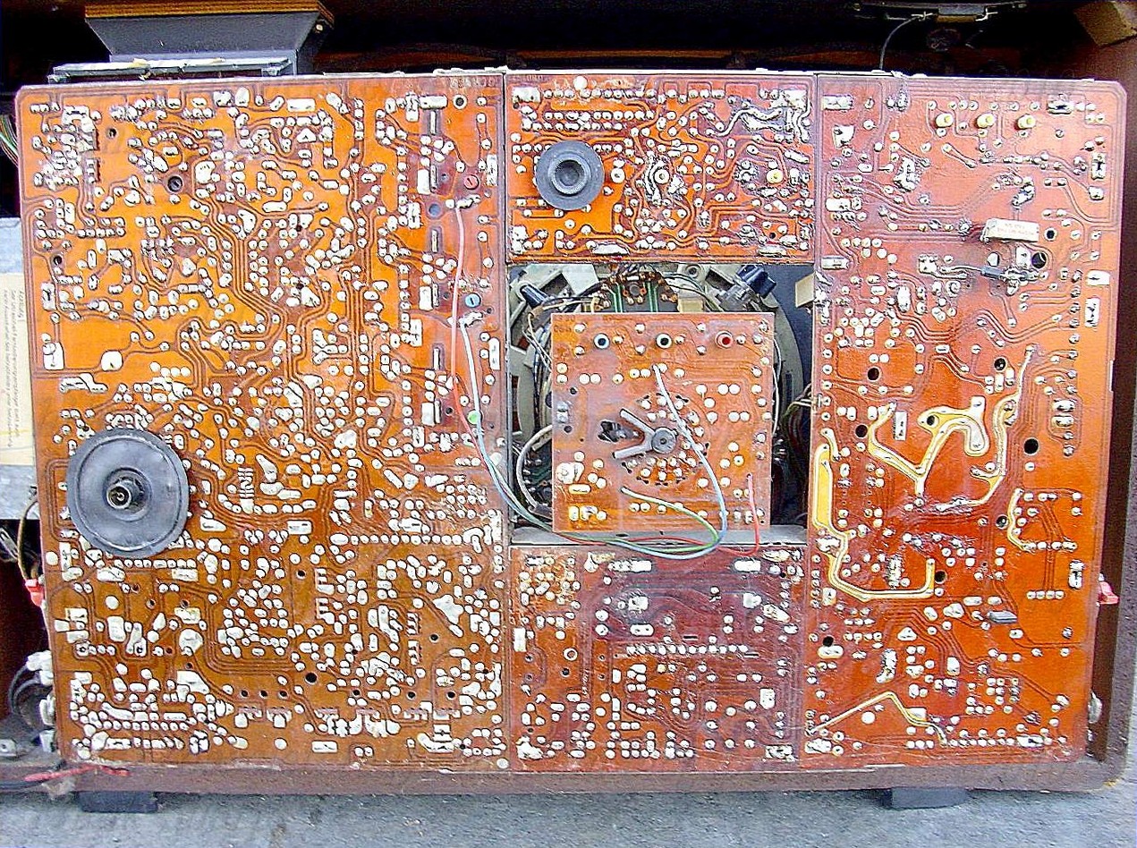
Note the PAL delay line ITT TAU50
first color television chassis from GRAETZ ITT (SEL) completely based on semiconductors discretes and only 3 IC's for the remote control circuits array.
Note the PAL delay line ITT TAU50
Showing even Units:
- convergence unit 455204c
- Remote control unit array 1 420502a itt saj110
- Remote control unit array 2 420503b
- Power supply drive control reg unit 435303
- convergence unit 455204c
- Remote control unit array 1 420502a itt saj110
- Remote control unit array 2 420503b
- Power supply drive control reg unit 435303
GRAETZ BURGGRAF COLOR 2549 ULTRASENSOR CHASSIS 5143 23 01Synchronized switch-mode power supply:
Line deflection EHT:In a switch mode power supply, a first switching transistor is coupled to a primary winding of an isolation transformer. A second switching transistor periodically applies a low impedance across a second winding of the transformer that is coupled to an oscillator for synchronizing the oscillator to the horizontal frequency. A third winding of the transformer is coupled via a switching diode to a capacitor of a control circuit for developing a DC control voltage in the capacitor that varies in accordance with a supply voltage B+. The control voltage is applied via the transformer to a pulse width modulator that is responsive to the oscillator output signal for producing a pulse-width modulated control signal. The control signal is applied to a mains coupled chopper transistor for generating and regulating the supply voltage B+ in accordance with the pulse width modulation of the control signal.
Description:
The invention relates to switch-mode power supplies.Some television receivers have signal terminals for receiving, for example, external video input signals such as R, G and B input signals, that are to be developed relative to the common conductor of the receiver. Such signal terminals and the receiver common conductor may be coupled to corresponding signal terminals and common conductors of external devices, such as, for example, a VCR or a teletext decoder.
To simplify the coupling of signals between the external devices and the television receiver, the common conductors of the receiver and of the external devices are connected together so that all are at the same potential. The signal lines of each external device are coupled to the corresponding signal terminals of the receiver. In such an arrangement, the common conductor of each device, such as of the television receiver, may be held "floating", or conductively isolated, relative to the corresponding AC mains supply source that energizes the device. When the common conductor is held floating, a user touching a terminal that is at the potential of the common conductor will not suffer an electrical shock.
Therefore, it may be desirable to isolate the common conductor, or ground, of, for example, the television receiver from the potentials of the terminals of the AC mains supply source that provide power to the television receiver. Such isolation is typically achieved by a transformer. The isolated common conductor is sometimes referred to as a "cold" ground conductor.
In a typical switch mode power supply (SMPS) of a television receiver the AC mains supply voltage is coupled, for example, directly, and without using transformer coupling, to a bridge rectifier. An unregulated direct current (DC) input supply voltage is produced that is, for example, referenced to a common conductor, referred to as "hot" ground, and that is conductively isolated from the cold ground conductor. A pulse width modulator controls the duty cycle of a chopper transistor switch that applies the unregulated supply voltage across a primary winding of an isolating flyback transformer. A flyback voltage at a frequency that is determined by the modulator is developed at a secondary winding of the transformer and is rectified to produce a DC output supply voltage such as a voltage B+ that energizes a horizontal deflection circuit of the televi
It may be desirable to synchronize the operation of the chopper transistor to horizontal scanning frequency for preventing the occurrence of an objectionable visual pattern in an image displayed in a display of the television receiver.
It may be further desirable to couple a horizontal synchronizing signal that is referenced to the cold ground to the pulse-width modulator that is referenced to the hot ground such that isolation is maintained.
CIRCUIT ARRANGEMENT IN A PICTURE DISPLAY DEVICE UTILIZING A STABILIZED SUPPLY VOLTAGE CIRCUIT:
Line synchronized switch mode power supply:GRAETZ BURGGRAF COLOR 2549 ULTRASENSOR CHASSIS 5143 23 01
A stabilized supply voltage circuit for a picture display device comprising a chopper wherein the switching signal has the line frequency and is duration-modulated. The coil of the chopper constitutes the primary winding of a transformer a secondary winding of which drives the line output transistor so that the switching transistor of the chopper also functions as a driver for the line output stage. The oscillator generating the switching signal may be the line oscillator. In a special embodiment the driver and line output transistor conduct simultaneously and in order to limit the base current of the line output transistor a coil shunted by a diode is incorporated in the drive line of the line output transistor. Other secondary windings of the transformer drive diodes which conduct simultaneously with the efficiency diode of the chopper so as to generate further stabilized supply voltages.

 1. An electrical circuit arrangement for a picture display device operating at a given line scanning frequency, comprising a source of unidirectional voltage, an inductor, first switching transistor means for periodically energizing said inductor at said scanning frequency with current from said source, an electrical load circuit coupled to said inductor and having applied thereto a voltage as determined by the ratio of the ON and OFF periods of said transistor, means for maintaining the voltage across said load circuit at a given value comprising means for comparing the voltage of said load circuit with a reference voltage, means responsive to departures of the value of the load circuit voltage from the value of said reference voltage for varying the conduction ratio of the ON and OFF periods of said transistor thereby to stabilize said load circuit voltage at the given value, a line deflection coil system for said picture display device, means for energizing said line deflection coil system from said load voltage circuit means, means for periodically interrupting the energization of said line deflection coil comprising second switching means and means coupled to said inductor for deriving therefrom a switching current in synchronism with the energization periods of said transistor and applying said switching current to said switching means thereby to actuate the same, and means coupled to said switching means and to said load voltage circuit for producing a voltage for energizing said 2. A circuit as claimed in claim 1 wherein the duty cycle of said switching 3. A circuit as claimed in claim 1 further comprising an efficiency first 4. A circuit as claimed in claim 3 further comprising at least a second diode coupled to said deriving means and to ground, and being poled to 5. A circuit as claimed in claim 1 wherein said second switching means comprises a second transistor coupled to said deriving means to conduct simultaneously with said first transistor, and further comprising a coil coupled between said driving means and said second transistor and a third diode shunt coupled to said coil and being poled to conduct when said 6. A circuit as claimed in claim 1 further comprising a horizontal oscillator coupled to said first transistor, said oscillator being the 7. A circuit as claimed in claim 1 further comprising means coupled to said inductor for deriving filament voltage for said display device.
Description:
The invention relates to a circuit arrangement in a picture display device wherein the input direct voltage between two input terminals, which is obtained be rectifying the mains alternating voltage, is converted into a stabilized output direct voltage by means of a switching transistor and a coil and wherein the transistor is connected to a first input terminal and an efficiency diode is connected to th
 e junction of the transistor and the coil. The switching transistor is driven by a pulsatory voltage of line frequency which pulses are duration-modulated in order to saturate the switching transistor during part of the period dependent on the direct voltage to be stabilized and to cut off this transistor during the remaining part of the period. The pulse duration modulation is effected by means of a comparison circuit which compares the direct voltage to be stabilized with a substantially constant voltage, the coil constituting the primary winding of a transformer.
 Such a circuit arrangement is known from German "Auslegeschrift" 1.293.304. wherein a circuit arrangement is described which has for its object to convert an input direct voltage which is generated between two terminals into a different direct voltage. The circuit employs a switch connected to the first terminal of the input voltage and periodically opens and closes so that the input voltage is converted into a pulsatory voltage. This pulsatory voltage is then applied to a coil. A diode is arranged between the junction of the switch and the coil and the second terminal of the input voltage whilst a load and a charge capacitor in parallel thereto are arranged between the other end of the coil and the second terminal of the input voltage. The assembly operates in accordance with the known efficiency principle i.e., the current supplied to the load flows alternately through the switch and through the diode. The function of the switch is performed by a switching transistor which is driven by a periodical pulsatory voltage which saturates this transistor for a given part of the period. Such a configuration is known under different names in the literature; it will be referred to herein as a "chopper." A known advantage thereof, is that the switching transistor must be able to stand a high voltage or provide a great current but it need not dissipate a great power. The output voltage of the chopper is compared with a constant reference voltage. If the output voltage attempts to vary because the input voltage and/or the load varies, a voltage causing a duration modulation of the pulses is produced at the output of the comparison arrangement. As a result the quantity of the energy stored in the coil varies and the output voltage is maintained constant. In the German "Auslegeschrift" referred to it is therefore an object to provide a stabilized supply voltage device.
In the circuit arrangement according to the mentioned German "Auslegeschrift" the frequency of the load variations or a harmonic thereof is chosen as the frequency for the switching voltage. Particularly when the load fed by the chopper is the line deflection circuit of a picture display device, wherein thus the impedance of the load varies in the rhythm of the line frequency, the frequency of the switching voltage is equal to or is a multiple of the line frequency.
 It is to be noted that the chopper need not necessarily be formed as that in the mentioned German "Auslegeschrift." In fact, it is known from literature that the efficiency diode and the coil may be exchanged. It is alternatively possible for the coil to be provided at the first terminal of the input voltage whilst the switching transistor is arranged between the other end and the second terminal of the input voltage. The efficiency diode is then provided between the junction of said end and the switching transistor and the load. It may be recognized that for all these modifications a voltage is present across the connections of the coil which voltage has the same frequency and the same shape as the pulsatory switching voltage. The control voltage of a line deflection circuit is a pulsatory voltage which causes the line output transistor to be saturates and cut off alternately. The invention is based on the recognition that the voltage present across the connections of the coil is suitable to function as such a control voltage and that the coil constitutes the primary of a transformer. To this end the circuit arrangement according to the invention is characterized in that a secondary winding of the transformer drives the switching element which applies a line deflection current to line deflection coils and by which the voltage for the final anode of a picture display tube which forms part of the picture display device is generated, and that the ratio between the period during which the switching transistor is saturated and the entire period, i.e., the switching transistor duty cycle is between 0.3 and 0.7 during normal operation.
The invention is also based on the recognition that the duration modulation which is necessary to stabilize the supply voltage with the switching transistor does not exert influence on the driving of the line output transistor. This resides in the fact that in case of a longer or shorter cut-off period of the line output transistor the current flowing through the line deflection coils thereof is not influenced because of the efficiency diode current and transistor current are taken over or, in case of a special kind of transistor, the collector-emitter current is taken over by the base collector current and conversely. However, in that case the above-mentioned ratios of 0.3 : 0.7 should be taken into account since otherwise this take-over principle is jeopardized.
As will be fu
 rther explained the use of the switching transistor as a driver for the line output transistor in an embodiment to be especially described hereinafter has the further advantage that the line output transistor automatically becomes non-conductive when this switching transistor is short circuited so that the deflection and the EHT for the display tube drop out and thus avoid damage thereof.
Due to the step according to the invention the switching transistor in the stabilized supply functions as a driver for the line deflection circuit. The circuit arrangement according to the invention may in addition be equipped with a very efficient safety circuit so that the reliability is considerably enhanced, which is described in the U.S. Pat. No. 3,629,686. The invention is furthermore based on the recognition of the fact that the pulsatory voltage present across the connections of the coil is furthermore used and to this end the circuit arrangement according to the invention is characterized in that secondary windings of the transformer drive diodes which conduct simultaneously with the efficiency diode so as to generate further stabilized direct voltages, one end of said diodes being connected to ground.
In order that the invention may be readily carried into effect, a few embodiments thereof will now be described in detail by way of example with reference to the accompanying diagrammatic drawings in which:
FIG. 1 shows a principle circuit diagram wherein the chopper and the line deflection circuit are further shown but other circuits are not further shown.
FIGS. 2a, 2b and 2c show the variation as a function of time of two currents and of a voltage occurring in the circuit arrangement according to FIG. 1.
FIGS. 3a 3b, 3c and 3d show other embodiments of the chopper.
FIGS. 4a and 4b show modifications of part of the circuit arrangement of FIG. 1.
 In FIG. 1 the reference numeral 1 denotes a rectifier circuit which converts the mains voltage supplied thereto into a non-stabilized direct voltage. The collector of a switching transistor 2 is connected to one of the two terminals between which this direct voltage is obtained, said transistor being of the npn-type in this embodiment and the base of which receives a pulsatory voltage which originates through a control stage 4 from a modulator 5 and causes transistor 2 to be saturated and cut off alternately. The voltage waveform 3 is produced at the emitter of transistor 2. In order to maintain the output voltage of the circuit arrangement constant, the duration of the pulses provided is varied in modulator 5. A pulse oscillator 6 supplies the pulsatory voltage to modulator 5 and is synchronized by a signal of line frequency which originates from the line oscillator 6' present in the picture display device. This line oscillator 6' is in turn directly synchronized in known manner by pulses 7' of line frequency which are present in the device and originate for example from a received television signal if the picture display device is a television receiver. Pulse oscillator 6 thus generates a pulsatory voltage the repetition frequency of which is the line frequency.
The emitter of switching transistor 2 is connected at one end to the cathode of an efficiency diode 7 whose other end is connected to the second input voltage terminal and at the other end to primary winding 8 of a transformer 9. Pulsatory voltage 3 which is produced at the cathode of efficiency diode 7 is clamped against the potential of said second terminal during the intervals when this diode conducts. During the other intervals the pulsatory voltage 3 assumes the value V i . A charge capacitor 10 and a load 11 are arranged between the other end of winding 8 and the second input voltage terminal. The elements 2,7,8,10 and 11 constitute a so-called chopper producing a direct voltage across charge capacitor 10, provided that capacitor 10 has a sufficiently great value for the line frequency and the current applied to load 11 flowing alternately through switching transistor 2 or through efficiency diode 7. The output voltage V o which is the direct voltage produced across charge capacitor 10 is applied to a comparison circuit 12 which compares the voltage V o with a reference voltage. Comparison circuit 12 generates a direct voltage which is applied to modulator 5 so that the duration of the effective period δ T of switching transistor 2 relative to the period T of pulses 3 varies as a function of the variations of output voltage V 0 . In fact, it is readily evident that output voltage V o is proportional to the ratio δ :
V o = V i . δ
Load 11 of the chopper consists in the consumption of parts of the picture display device which are fed by output voltage V 0 . In a practical embodiment of the circuit arrangement according to FIG. 1 wherein the mains alternating voltage has a nominal effective value of 220 V and the rectified voltage V i is approximately 270 V, output voltage V o for δ = 0.5 is approximately 135 V. This makes it also possible, for example, to feed a line deflection circuit as is shown in FIG. 1 wherein load 11 then represents different parts which are fed by the chopper. Since voltage V o is maintained constant due to pulse duration modulation, the supply voltage of this line deflection circuit remains constant with the favorable result that the line amplitude(= the width of the picture displayed on the screen of the picture display tube) likewise remains constant as well as the EHT required for the final anode of the picture display tube in the same circuit arrangement independent of the variations in the mains voltage and the load on the EHT generator (= variations in brightness).
However, variations in the line amplitude and the EHT may occur as a result of an insufficiently small internal impedance of the EHT generator. Compensation means are known for this purpose. A possibility within the scope of the present invention is to use comparison circuit 12 for this purpose. In fact, if the beam current passes through an element having a substantially quadratic characteristic, for example, a voltage-dependent resistor, then a variation for voltage V o may be obtained through comparison circuit 12 which variation is proportional to the root of the variation in the EHT which is a known condition for the line amplitude to remain constant.

 In addition this facilitates smoothing of voltage V o since the repetition frequency of pulsatory voltage 3 is many times higher than that of the mains and a comparatively small value may be sufficient for charge capacitor 10. If charge capacitor 10 has a sufficiently high value for the line frequency, voltage V o is indeed a direct voltage so that a voltage having the same form as pulsatory voltage 3 is produced across the terminals of primary winding 8. Thus voltages which have the same shape as pulsatory voltage 3 but have a greater or smaller amplitude are produced across secondary windings 13, 14 of transformer 9 (FIG. 1 shows only 2 secondary windings but there may be more). The invention is based on the recognition that one end of each secondary winding is connected to earth while the other end thereof drives a diode, the winding sense of each winding and the direction of conductance of each diode being chosen to be such that these diodes conduct during the same period as does efficiency diode 7. After smoothing, stabilized supply voltages, for example, at terminal 15 are generated in this manner at the amplitudes and polarities required for the circuit arrangements present in the picture display device. In FIG. 1 the voltage generated at terminal 15 is, for example, positive relative to earth. It is to be noted that the load currents of the supply voltages obtained in this manner cause a reduction of the switching power which is economized by efficiency diode 7. The sum of all diode currents including that of diode 7 is in fact equal to the current which would flow through diode 7 if no secondary winding were wound on transformer 9 and if no simultaneous diode were used. This reduction may be considered an additional advantage of the circuit arrangement according to the invention, for a diode suitable for smaller powers may then be used. However, it will be evident that the overall secondary load must not exceed the primary load since otherwise there is the risk of efficiency diode 7 being blocked so that stabilization of the secondary supply voltages would be out of the question.
I
t is to be noted that a parabola voltage of line frequency as shown at 28 is produced across the charge capacitor 10 if this capacitor is given a smaller capacitance so that consequently the so-called S-correction is established.
In FIG. 1 charge capacitors are arranged between terminals 15 etc. and earth so as to ensure that the voltages on these points are stabilized direct voltages. If in addition the mean value of the voltage on one of these terminals has been made equal to the effective value of the alternating voltage which is required for heating the filament of the picture display tube present in the picture display device, this voltage is suitable for this heating. This is a further advantage of the invention since the cheap generation of a stabilized filament voltage for the picture display tube has always been a difficult problem in transistorized arrangements.
A further advantage of the picture display device according to the invention is that transformer 9 can function as a separation transformer so that the different secondary windings can be separated from the mains and their lower ends can be connected to ground of the picture display device. The latter step makes it possible to connect a different apparatus such as, for example, a magnetic recording and/or playback apparatus to the picture display device without earth connection problems occurring.
In FIG. 1 the reference numeral 14 denotes a secondary winding of transformer 9 which in accordance with the previously mentioned recognition of the invention can drive line output transistor 16 of the line deflection circuit 17. Line deflection circuit 17 which is shown in a simplified form in FIG. 1 includes inter alia line deflection coils 18 and an EHT transformer 19 a secondary winding 20 of which serves for generating the EHT required for the acceleration anode of the picture display tube. Line deflection circuit 17 is fed by the output voltage V o of the chopper which voltage is stabilized due to the pulse duration modulation with all previously mentioned advantages. Line deflection circuit 17 corresponds, for example, to similar arrangements which have been described in U.S. Pat. No. 3,504,224 issued Mar. 31, 1970 to J.J. Reichgelt et al., U.S. patent application Ser. No. 737,009 filed June 14, 1968 by W. H. Hetterscheid and U.S. application Ser. No. 26,497 filed April 8, 1970 by W. Hetterscheid et al. It will be evident that differently formed lined deflection circuits are alternatively possible.
It will now be shown that secondary winding 14 can indeed drive a line deflection circuit so that switching transistor 2 can function as a driver for the line deflection. FIGS. 2a and b show the variation as a function of time of the current i C which flows in the collector of transistor 16 and of the drive voltage v 14 across the terminals of secondary winding 14. During the flyback period (0, t 1 ) transistor 16 must be fully cut off because a high voltage peak is then produced at its collector; voltage v 14 must then be absolutely negative. During the scan period (t 1 , t 4 ) a sawtooth current i C flows through the collector electrode of transistor 16 which current is first negative and then changes its direction. As the circuit arrangement is not free from loss, the instant t 3 when current i C becomes zero lies, as is known, before the middle of the scan period. At the end t 4 of the scan period transistor 16 must be switched off again. However, since transistor 16 is saturated during the scan period and since this transistor must be suitable for high voltages and great powers so that its collector layer is thick, this transistor has a very great excess of charge carriers in both its base and collector layers. The removal of these charge carriers takes a period t s which is not negligible whereafter the transistor is indeed switched off. Thus the fraction δ T of the line period T at which v 14 is positive must end at the latest at the instant (t 4 - t s ) located after the commencement (t = 0) of the previous flyback.
The time δ T may be initiated at any instant t 2 which is located between the end t 1 of the flyback period and the instant t 3 when collector current i C reverses its direction. It is true that emitter current flows through transistor 16 at the instant t 2 , but collector current i C is not influenced thereby, at least not when the supply voltage (= V o ) for line deflection circuit 17 is high enough. All this has been described in the U.S. Pat. No. 3,504,224. The same applies to line deflection
 circuits wherein the collector base diode does not function as an efficiency diode as is the case in the described circuit 17, but wherein an efficiency diode is arranged between collector and emitter of the line output transistor. In such a case the negative part of the current i C of FIG. 2a represents the current flowing through the said efficiency diode.
After the instant t 3 voltage v 14 must be positive. In other words, the minimum duration of the period T when voltage v 14 must be positive is (t 4 - t s ) - t 3 whilst the maximum duration thereof is (t 4 - t s ) - t 1 . In a television system employing 625 lines per raster the line period t 4 is approximately 64 μus and the flyback period is approximately 12 μus. Without losses in the circuit arrangement instant t 3 would be located approximately 26 μus after the instant t 1 , and with losses a reasonable value is 22 μus which is 34 μus after the commencement of the period. If for safety's sake it is assumed that t s lasts approximately 10 μus, the extreme values of δ T are approximately 20 and 42 μus and consequently the values for δ are approximately 0.31 and 0.66 at a mean value which is equal to approximately 0.49. It was previously stated that a mean value of δ = 0.5 was suitable. Line deflection circuit 17 can therefore indeed be used in combination with the chopper in the manner described, and the relative variation of δ may be (0.66 - 0.31) : 0.49 = 71.5 percent. This is more than necessary to obviate the variations in the mains voltage or in the various loads and to establish the East-West modulation and ripple compensation to be described hereinafter. In fact, if it is assumed that the mains voltage varies between -15 and +10 percent of the nominal value of 220 V, while the 50 Hz ripple voltage which is superimposed on the input voltage V i has a peak-to-peak value of 40 V and V i is nominally 270 V, then the lowest occurring V i is:
0.85 × 270 V - 20 V = 210 V and the highest occurring V i is
1.1 × 270 V + 20 V = 320 V. For an output voltage V o of 135 V the ratio must thus vary between
δ = 135 : 210 = 0.64 and δ = 135 : 320 = 0.42.
A considerable problem presenting itself is that of the simultaneous or non-simultaneous drive of line output transistor 16 with switching transistor 2, it being understood that in case of simultaneous drive both transistors are simultaneously bottomed, that is during the period δ T. This depends on the winding sense of secondary winding 14 relative to that of primary winding 8. In FIG. 1 it has been assumed that the drive takes place simultaneously so that the voltage present across winding 14 has the shape shown in FIG. 2b. This voltage assumes the value n(V i - V o ) in the period δ T and the value -nVo in the period (1 - δ )T, wherein n is the ratio of the number of turns on windings 14 and 8 and wherein V o is maintained constant at nominal mains voltage V o = δ V inom . However, if as a result of an increase or a decrease of the mains voltage V i increases or decreases proportionally therewith, i.e., V i = V i nom + Δ V, the positive portion of V 14 becomes equal to n(V i nom - V o +Δ V) = n [(1 -δ)V i nom +ΔV] = n(0.5 V inom +ΔV) if δ = 0.5 for V i = V i nom. Relatively, this is a variation which is twice as great. For example, if V i nom = 270 V and V o = 135 V, a variation in the mains voltage of from -15 to +10 percent causes a variation of V i of from -40.5 V to +27 V which ranges from -30 to +20 percent of 135 V which is present across winding 8 during the period δ T. The result is that transistor 16 can always be bottomed over a large range of variation. If the signal of FIG. 2b would be applied through a resistor to the base of transistor 16, the base current thereof would have to undergo the same variation while the transistor would already be saturated in case of too low a voltage. In this case it is assumed that transformer 9 is ideal (without loss) and that coil 21 has a small inductance as is explained in the U.S. patent application Ser. No. 737,009 above mentioned. It is therefore found to be desirable to limit the base current of transistor 16.
This may be effected by providing a coil 22 having a large value inductance, approximately 100 μH, between winding 14 and the small coil 21. The variation of said base current i b is shown in FIG. 2c but not to the same scale as the collector current of FIG. 2a. During the conducting interval δ T current i b varies as a linear function of time having a final value of wherein L represents the inductance of coil 22. This not only provides the advantage that this final value is not immediately reached, but it can be shown that variation of this final value as a function of the mains voltage has been reduced, for there applies at nominal mains voltage that: If the mains voltage V i = V i nom +Δ V, then ##SPC1## because V i nom = 2 V o . Thus this variation is equal to that of the mains voltage and is not twice as great.
 During switching off, t 2 , of transistor 16 coil 22 must exert no influence and coil 21 must exert influence which is achieved by arranging a diode 23 parallel to coil 22. Furthermore the control circuit of transistor 16 in this example comprises the two diodes 24 and 25 as described in U.S. application Ser. No. 26,497 above referred to, wherein one of these diodes, diode 25 in FIG. 1, must be shunted by a resistor.
The control circuit of transistor 16 may alternatively be formed as is shown in FIG. 4. In fact, it is known that coil 21 may be replaced by the parallel arrangement of a diode 21' and a resistor 21" by which the inverse current can be limited. To separate the path of the inverse current from that of the forward current the parallel arrangement of a the diode 29' and a resistor 29" must then be present. This leads to the circuit arrangement shown in the upper part of FIG. 4. This circuit arrangement may now be simplified if it is noted that diodes 25 and 21' on the one hand and diodes 23 and 29' on the other hand are series-arranged. The result is shown in the lower part of FIG. 4 which, as compared with the circuit arrangement of FIG. 1, employs one coil less and an additional resistor.
FIG. 3 shows possible modifications of the chopper. FIG. 3a shown in a simplified form the circuit arrangement according to FIG. 1 wherein the pulsatory voltage present across the connections of windings 8 has a peak-to-peak amplitude of V i - V o = 0.5 V i for δ = 0.5, As has been stated, the provision of coil 22 gives a relative variation for the base current of transistor 16 which is equal to that of the mains voltage. In the cases according to FIG. 3b, 3c and 3d the peak-to-peak amplitude of the voltage across winding 8 is equal to V i so that the provision of coil 22 results in a relative variation which is equal to half that of the mains voltage which is still more favorable than in the first case.
Transistors of the npn type are used in FIG. 3. If transistors of the pnp type are used, the relevant efficiency diodes must of course be reversed.
In this connection it is to be noted that it is possible to obtain an output voltage V o with the aid of the modifications according to FIGS. 3b, c and d, which voltage is higher than input voltage V i . These modifications may be used in countries such as, for example, the United of America or France where the nominal mains voltage is 117 or 110 V without having to modify the rest of the circuit arrangement.
The above-mentioned remark regarding the sum of the diode currents only applies, however, for the modifications shown in FIGS. 3a and d.
If line output transistor 16 is not simultaneously driven with switching transistor 2, efficiency diodes 7 conducts simultaneously with transistor 16 i.e., during the period which is denoted by δ T in FIGS. 1 and 2b. During that period the output voltage V o of the chopper is stabilized so that the base current of transistor 16 is stabilized without further difficulty. However, a considerable drawback occurs. In FIG. 1 the reference numeral 26 denotes a safety circuit the purpose of which is to safeguard switching transistor 2 when the current supplied to load 11 and/or line deflection circuit 17 becomes to high, which happens because the chopper stops. After a given period output voltage V o is built up again, but gradually which means that the ratio δ is initially small in the order of 0.1. All this is described in U.S. patent No. 3,629,686. The same phenomenon occurs when the display device is switched on. Since δ = 0.1 corresponds to approximately 6 μs when T = 64 μs, efficiency diode 7 c
 onducts in that case for 64 - 6 = 58 μus so that transistor 16 is already switched on at the end of the scan or at a slightly greater ratio δ during the flyback. This would cause an inadmissibly high dissipation. For this reason the simultaneous drive is therefore to be preferred.
The line deflection circuit itself is also safeguarded: in fact, if something goes wrong in the supply, the driver voltage of the line deflection circuit drops out because the switching voltage across the terminals of primary winding 8 is no longer present so that the deflection stops. This particularly happens when switching transistor 2 starts to constitute a short-circuit between emitter and collector with the result that the supply voltage V o for the line deflection circuit in the case of FIG. 1 becomes higher, namely equal to V i . However, the line output transformer is now cut off and is therefore also safe as well as the picture display tube and other parts of the display device which are fed by terminal 15 or the like. However, this only applies to the circuit arrangement according to FIG. 1 or 3a.
 Pulse oscillator 6 applies pulses of line frequency to modulator 5. It may be advantageous to have two line frequency generators as already described, to wit pulse oscillator 6 and line oscillator 6' which is present in the picture display device and which is directly synchronized in known manner by line synchronizing pulses 7'. In fact, in this case line oscillator 6' applies a signal of great amplitude and free from interference to pulse oscillator 6. However, it is alternatively possible to combine pulse oscillator 6 and line oscillator 6' in one single oscillator 6" (see FIG. 1) which results in an economy of components. It will be evident that line oscillator 6' and oscillator 6" may alternatively be synchronized indirectly, for example, by means of a phase discriminator. It is to be noted neither pulse oscillator 6, line oscillator 6' and oscillator 6" nor modulator 5 can be fed by the supply described since output voltage V o is still not present when the mains voltage is switched on. Said circuit arrangements must therefore be fed directly from the input terminals. If as described above these circuit arrangements are to be separated from the mains, a small separation transformer can be used whose primary winding is connected between the mains voltage terminals and whose secondary winding is connected to ground at one end and controls a rectifier at the other end.
Capacitor 27 is arranged parallel to efficiency diode 7 so as to reduce the dissipation in switching transistor 2. In fact, if transistor 2 is switched off by the pulsatory control voltage, its collector current decreases and its collector-emitter voltage increases simultaneously so that the dissipated power is not negligible before the collector current has becomes zero. If efficiency diode 7 is shunted by capacitor 27 the increase of the collector-emitter voltage is delayed i.e., this voltage does not assume high values until the collector current has already been reduced. It is true that in that case the dissipation in transistor 2 slightly increases when it is switched on by the pulsatory control voltage but on the other hand since the current flowing through diode 7 has decreased due to the presence of the secondary windings, its inverse current is also reduced when transistor 2 is switched on and hence its dissipation has become smaller. In addition it is advantageous to delay these switching-on and switching-off periods to a slight extent because the switching pulses then contain fewer Fourier components of high frequency which may cause interferences in the picture display device and which may give rise to visible interferences on the screen of the display tube. These interferences occupy a fixed position on the displayed image because the switching frequency is the line frequency which is less disturbing to the viewer. In a practical ci
rcuit wherein the line frequency is 15,625 Hz and wherein switching transistor 2 is an experimental type suitable for a maximum of 350 V collector-emitter voltage or 1 A collector current and wherein efficiency diode 7 is of the Philips type BA 148 the capacitance of capacitor 27 is approximately 680 pF whilst the load is 70 W on the primary and 20 W on the secondary side of transformer 9. The collector dissipation upon switching off is 0.3 W (2.5 times smaller than without capacitor 27) and 0.7 W upon switching on.
As is known the so-called pincushion distortion is produced in the picture display tubes having a substantially flat screen and large deflection angles which are currently used. This distortion is especially a problem in color television wherein a raster correction cannot be brought about by magnetic means. The correction of the so-called East-West pincushion distortion i.e., in the horizontal direction on the screen of the picture display tube can be established in an elegant manner with the aid of the circuit arrangement according to the invention. In fact, if the voltage generated by comparison circuit 12 and being applied to modulator 5 for duration-modulating pulsatory voltage 3 is modulated by a parabola voltage 28 of field frequency, pulsatory voltage 3 is also modulated thereby. If the power consumption of the line deflection circuit forms part of the load on the output voltage of the chopper, the signal applied to the line deflection coils is likewise modulated in the same manner. Conditions therefore are that the parabola voltage 28 of field frequency has a polarity such that the envelope of the sawtooth current of line frequency flowing through the line deflection coils has a maximum in the middle of the scan of the field period and that charge capacitor 10 has not too small an impedance for the field frequency. On the other hand the other supply voltages which are generated by the circuit arrangement according to the invention and which might be hampered by this component of field frequency must be smoothed satisfactorily.
A practical embodiment of the described example with the reference numerals given provides an output for the supply of approximately 85 percent at a total load of 90 W, the internal resistance for direct current loads being 1.5 ohms and for pulsatory currents being approximately 10 ohms. In case of a variation of ± 10 percent of the mains voltage, output voltage V o is stable within 0.4 V. Under the nominal circumstances the collector dissipation of switching transistor 2 is approximately 2.5 W.
Since the internal resistance of the supply is so small, it can be used advantageously, for example, at terminal 15 for supplying a class-B audio amplifier which forms part of the display device. Such an amplifier has the known advantages that its dissipation is directly proportional to the amplitude of the sound to be reproduced and that its output is higher than that of a class-A amplifier. On the other hand a class-A amplifier consumes a substantially constant power so that the internal resistance of the supply voltage source is of little importance. However, if this source is highly resistive, the supply voltage is modulated in the case of a class-B amplifier by the audio information when the sound intensity is great which may detrimentally influence other parts of the display device. This drawback is prevented by means of the supply according to the invention.
 The 50 Hz ripple voltage which is superimposed on the rectified input voltage V i is compensated by comparison circuit 12 and modulator 5 since this ripple voltage may be considered to be a variation of input voltage V i . A further compensation is obtained by applying a portion of this ripple voltage with suitable polarity to comparison circuit 12. It is then sufficient to have a lower value for the smoothing capacitor which forms part of rectifier circuit 1 (see FIG. 3). The parabola voltage 28 of field frequency originating from the field time base is applied to the same circuit 12 so as to correct the East-West pincushion distortion .
Switch-mode power supply generating a variable pulse-width modulating signal by digital control techniques synchronized with the horizontal line rate of the receiver. Logic circuits operating against fixed references provide overload and short-circuit protection by rapidly decreasing the variable pulse-width signal duration during various fault conditions.
Such a circuit arrangement is known from German "Auslegeschrift" 1.293.304. wherein a circuit arrangement is described which has for its object to convert an input direct voltage which is generated between two terminals into a different direct voltage. The circuit employs a switch connected to the first terminal of the input voltage and periodically opens and closes so that the input voltage is converted into a pulsatory voltage. This pulsatory voltage is then applied to a coil. A diode is arranged between the junction of the switch and the coil and the second terminal of the input voltage whilst a load and a charge capacitor in parallel thereto are arranged between the other end of the coil and the second terminal of the input voltage. The assembly operates in accordance with the known efficiency principle i.e., the current supplied to the load flows alternately through the switch and through the diode. The function of the switch is performed by a switching transistor which is driven by a periodical pulsatory voltage which saturates this transistor for a given part of the period. Such a configuration is known under different names in the literature; it will be referred to herein as a "chopper." A known advantage thereof, is that the switching transistor must be able to stand a high voltage or provide a great current but it need not dissipate a great power. The output voltage of the chopper is compared with a constant reference voltage. If the output voltage attempts to vary because the input voltage and/or the load varies, a voltage causing a duration modulation of the pulses is produced at the output of the comparison arrangement. As a result the quantity of the energy stored in the coil varies and the output voltage is maintained constant. In the German "Auslegeschrift" referred to it is therefore an object to provide a stabilized supply voltage device.In the circuit arrangement according to the mentioned German "Auslegeschrift" the frequency of the load variations or a harmonic thereof is chosen as the frequency for the switching voltage. Particularly when the load fed by the chopper is the line deflection circuit of a picture display device, wherein thus the impedance of the load varies in the rhythm of the line frequency, the frequency of the switching voltage is equal to or is a multiple of the line frequency.
It is to be noted that the chopper need not necessarily be formed as that in the mentioned German "Auslegeschrift." In fact, it is known from literature that the efficiency diode and the coil may be exchanged. It is alternatively possible for the coil to be provided at the first terminal of the input voltage whilst the switching transistor is arranged between the other end and the second terminal of the input voltage. The efficiency diode is then provided between the junction of said end and the switching transistor and the load. It may be recognized that for all these modifications a voltage is present across the connections of the coil which voltage has the same frequency and the same shape as the pulsatory switching voltage. The control voltage of a line deflection circuit is a pulsatory voltage which causes the line output transistor to be saturates and cut off alternately. The invention is based on the recognition that the voltage present across the connections of the coil is suitable to function as such a control voltage and that the coil constitutes the primary of a transformer. To this end the circuit arrangement according to the invention is characterized in that a secondary winding of the transformer drives the switching element which applies a line deflection current to line deflection coils and by which the voltage for the final anode of a picture display tube which forms part of the picture display device is generated, and that the ratio between the period during which the switching transistor is saturated and the entire period, i.e., the switching transistor duty cycle is between 0.3 and 0.7 during normal operation.The invention is also based on the recognition that the duration modulation which is necessary to stabilize the supply voltage with the switching transistor does not exert influence on the driving of the line output transistor. This resides in the fact that in case of a longer or shorter cut-off period of the line output transistor the current flowing through the line deflection coils thereof is not influenced because of the efficiency diode current and transistor current are taken over or, in case of a special kind of transistor, the collector-emitter current is taken over by the base collector current and conversely. However, in that case the above-mentioned ratios of 0.3 : 0.7 should be taken into account since otherwise this take-over principle is jeopardized.
As will be fu
Due to the step according to the invention the switching transistor in the stabilized supply functions as a driver for the line deflection circuit. The circuit arrangement according to the invention may in addition be equipped with a very efficient safety circuit so that the reliability is considerably enhanced, which is described in the U.S. Pat. No. 3,629,686. The invention is furthermore based on the recognition of the fact that the pulsatory voltage present across the connections of the coil is furthermore used and to this end the circuit arrangement according to the invention is characterized in that secondary windings of the transformer drive diodes which conduct simultaneously with the efficiency diode so as to generate further stabilized direct voltages, one end of said diodes being connected to ground.
In order that the invention may be readily carried into effect, a few embodiments thereof will now be described in detail by way of example with reference to the accompanying diagrammatic drawings in which:
FIG. 1 shows a principle circuit diagram wherein the chopper and the line deflection circuit are further shown but other circuits are not further shown.
FIGS. 2a, 2b and 2c show the variation as a function of time of two currents and of a voltage occurring in the circuit arrangement according to FIG. 1.
FIGS. 3a 3b, 3c and 3d show other embodiments of the chopper.
FIGS. 4a and 4b show modifications of part of the circuit arrangement of FIG. 1.
 In FIG. 1 the reference numeral 1 denotes a rectifier circuit which converts the mains voltage supplied thereto into a non-stabilized direct voltage. The collector of a switching transistor 2 is connected to one of the two terminals between which this direct voltage is obtained, said transistor being of the npn-type in this embodiment and the base of which receives a pulsatory voltage which originates through a control stage 4 from a modulator 5 and causes transistor 2 to be saturated and cut off alternately. The voltage waveform 3 is produced at the emitter of transistor 2. In order to maintain the output voltage of the circuit arrangement constant, the duration of the pulses provided is varied in modulator 5. A pulse oscillator 6 supplies the pulsatory voltage to modulator 5 and is synchronized by a signal of line frequency which originates from the line oscillator 6' present in the picture display device. This line oscillator 6' is in turn directly synchronized in known manner by pulses 7' of line frequency which are present in the device and originate for example from a received television signal if the picture display device is a television receiver. Pulse oscillator 6 thus generates a pulsatory voltage the repetition frequency of which is the line frequency.
 The emitter of switching transistor 2 is connected at one end to the cathode of an efficiency diode 7 whose other end is connected to the second input voltage terminal and at the other end to primary winding 8 of a transformer 9. Pulsatory voltage 3 which is produced at the cathode of efficiency diode 7 is clamped against the potential of said second terminal during the intervals when this diode conducts. During the other intervals the pulsatory voltage 3 assumes the value V i . A charge capacitor 10 and a load 11 are arranged between the other end of winding 8 and the second input voltage terminal. The elements 2,7,8,10 and 11 constitute a so-called chopper producing a direct voltage across charge capacitor 10, provided that capacitor 10 has a sufficiently great value for the line frequency and the current applied to load 11 flowing alternately through switching transistor 2 or through efficiency diode 7. The output voltage V o which is the direct voltage produced across charge capacitor 10 is applied to a comparison circuit 12 which compares the voltage V o with a reference voltage. Comparison circuit 12 generates a direct voltage which is applied to modulator 5 so that the duration of the effective period δ T of switching transistor 2 relative to the period T of pulses 3 varies as a function of the variations of output voltage V 0 . In fact, it is readily evident that output voltage V o is proportional to the ratio δ :
V o = V i . δ
Load 11 of the chopper consists in the consumption of parts of the picture display device which are fed by output voltage V 0 . In a practical embodiment of the circuit arrangement according to FIG. 1 wherein the mains alternating voltage has a nominal effective value of 220 V and the rectified voltage V i is approximately 270 V, output voltage V o for δ = 0.5 is approximately 135 V. This makes it also possible, for example, to feed a line deflection circuit as is shown in FIG. 1 wherein load 11 then represents different parts which are fed by the chopper. Since voltage V o is maintained constant due to pulse duration modulation, the supply voltage of this line deflection circuit remains constant with the favorable result that the line amplitude(= the width of the picture displayed on the screen of the picture display tube) likewise remains constant as well as the EHT required for the final anode of the picture display tube in the same circuit arrangement independent of the variations in the mains voltage and the load on the EHT generator (= variations in brightness).
However, variations in the line amplitude and the EHT may occur as a result of an insufficiently small internal impedance of the EHT generator. Compensation means are known for this purpose. A possibility within the scope of the present invention is to use comparison circuit 12 for this purpose. In fact, if the beam current passes through an element having a substantially quadratic characteristic, for example, a voltage-dependent resistor, then a variation for voltage V o may be obtained through comparison circuit 12 which variation is proportional to the root of the variation in the EHT which is a known condition for the line amplitude to remain constant.In addition this facilitates smoothing of voltage V o since the repetition frequency of pulsatory voltage 3 is many times higher than that of the mains and a comparatively small value may be sufficient for charge capacitor 10. If charge capacitor 10 has a sufficiently high value for the line frequency, voltage V o is indeed a direct voltage so that a voltage having the same form as pulsatory voltage 3 is produced across the terminals of primary winding 8. Thus voltages which have the same shape as pulsatory voltage 3 but have a greater or smaller amplitude are produced across secondary windings 13, 14 of transformer 9 (FIG. 1 shows only 2 secondary windings but there may be more). The invention is based on the recognition that one end of each secondary winding is connected to earth while the other end thereof drives a diode, the winding sense of each winding and the direction of conductance of each diode being chosen to be such that these diodes conduct during the same period as does efficiency diode 7. After smoothing, stabilized supply voltages, for example, at terminal 15 are generated in this manner at the amplitudes and polarities required for the circuit arrangements present in the picture display device. In FIG. 1 the voltage generated at terminal 15 is, for example, positive relative to earth. It is to be noted that the load currents of the supply voltages obtained in this manner cause a reduction of the switching power which is economized by efficiency diode 7. The sum of all diode currents including that of diode 7 is in fact equal to the current which would flow through diode 7 if no secondary winding were wound on transformer 9 and if no simultaneous diode were used. This reduction may be considered an additional advantage of the circuit arrangement according to the invention, for a diode suitable for smaller powers may then be used. However, it will be evident that the overall secondary load must not exceed the primary load since otherwise there is the risk of efficiency diode 7 being blocked so that stabilization of the secondary supply voltages would be out of the question.I
In FIG. 1 charge capacitors are arranged between terminals 15 etc. and earth so as to ensure that the voltages on these points are stabilized direct voltages. If in addition the mean value of the voltage on one of these terminals has been made equal to the effective value of the alternating voltage which is required for heating the filament of the picture display tube present in the picture display device, this voltage is suitable for this heating. This is a further advantage of the invention since the cheap generation of a stabilized filament voltage for the picture display tube has always been a difficult problem in transistorized arrangements.
A further advantage of the picture display device according to the invention is that transformer 9 can function as a separation transformer so that the different secondary windings can be separated from the mains and their lower ends can be connected to ground of the picture display device. The latter step makes it possible to connect a different apparatus such as, for example, a magnetic recording and/or playback apparatus to the picture display device without earth connection problems occurring.
In FIG. 1 the reference numeral 14 denotes a secondary winding of transformer 9 which in accordance with the previously mentioned recognition of the invention can drive line output transistor 16 of the line deflection circuit 17. Line deflection circuit 17 which is shown in a simplified form in FIG. 1 includes inter alia line deflection coils 18 and an EHT transformer 19 a secondary winding 20 of which serves for generating the EHT required for the acceleration anode of the picture display tube. Line deflection circuit 17 is fed by the output voltage V o of the chopper which voltage is stabilized due to the pulse duration modulation with all previously mentioned advantages. Line deflection circuit 17 corresponds, for example, to similar arrangements which have been described in U.S. Pat. No. 3,504,224 issued Mar. 31, 1970 to J.J. Reichgelt et al., U.S. patent application Ser. No. 737,009 filed June 14, 1968 by W. H. Hetterscheid and U.S. application Ser. No. 26,497 filed April 8, 1970 by W. Hetterscheid et al. It will be evident that differently formed lined deflection circuits are alternatively possible.
It will now be shown that secondary winding 14 can indeed drive a line deflection circuit so that switching transistor 2 can function as a driver for the line deflection. FIGS. 2a and b show the variation as a function of time of the current i C which flows in the collector of transistor 16 and of the drive voltage v 14 across the terminals of secondary winding 14. During the flyback period (0, t 1 ) transistor 16 must be fully cut off because a high voltage peak is then produced at its collector; voltage v 14 must then be absolutely negative. During the scan period (t 1 , t 4 ) a sawtooth current i C flows through the collector electrode of transistor 16 which current is first negative and then changes its direction. As the circuit arrangement is not free from loss, the instant t 3 when current i C becomes zero lies, as is known, before the middle of the scan period. At the end t 4 of the scan period transistor 16 must be switched off again. However, since transistor 16 is saturated during the scan period and since this transistor must be suitable for high voltages and great powers so that its collector layer is thick, this transistor has a very great excess of charge carriers in both its base and collector layers. The removal of these charge carriers takes a period t s which is not negligible whereafter the transistor is indeed switched off. Thus the fraction δ T of the line period T at which v 14 is positive must end at the latest at the instant (t 4 - t s ) located after the commencement (t = 0) of the previous flyback.
The time δ T may be initiated at any instant t 2 which is located between the end t 1 of the flyback period and the instant t 3 when collector current i C reverses its direction. It is true that emitter current flows through transistor 16 at the instant t 2 , but collector current i C is not influenced thereby, at least not when the supply voltage (= V o ) for line deflection circuit 17 is high enough. All this has been described in the U.S. Pat. No. 3,504,224. The same applies to line deflection
After the instant t 3 voltage v 14 must be positive. In other words, the minimum duration of the period T when voltage v 14 must be positive is (t 4 - t s ) - t 3 whilst the maximum duration thereof is (t 4 - t s ) - t 1 . In a television system employing 625 lines per raster the line period t 4 is approximately 64 μus and the flyback period is approximately 12 μus. Without losses in the circuit arrangement instant t 3 would be located approximately 26 μus after the instant t 1 , and with losses a reasonable value is 22 μus which is 34 μus after the commencement of the period. If for safety's sake it is assumed that t s lasts approximately 10 μus, the extreme values of δ T are approximately 20 and 42 μus and consequently the values for δ are approximately 0.31 and 0.66 at a mean value which is equal to approximately 0.49. It was previously stated that a mean value of δ = 0.5 was suitable. Line deflection circuit 17 can therefore indeed be used in combination with the chopper in the manner described, and the relative variation of δ may be (0.66 - 0.31) : 0.49 = 71.5 percent. This is more than necessary to obviate the variations in the mains voltage or in the various loads and to establish the East-West modulation and ripple compensation to be described hereinafter. In fact, if it is assumed that the mains voltage varies between -15 and +10 percent of the nominal value of 220 V, while the 50 Hz ripple voltage which is superimposed on the input voltage V i has a peak-to-peak value of 40 V and V i is nominally 270 V, then the lowest occurring V i is:
0.85 × 270 V - 20 V = 210 V and the highest occurring V i is
1.1 × 270 V + 20 V = 320 V. For an output voltage V o of 135 V the ratio must thus vary between
δ = 135 : 210 = 0.64 and δ = 135 : 320 = 0.42.
A considerable problem presenting itself is that of the simultaneous or non-simultaneous drive of line output transistor 16 with switching transistor 2, it being understood that in case of simultaneous drive both transistors are simultaneously bottomed, that is during the period δ T. This depends on the winding sense of secondary winding 14 relative to that of primary winding 8. In FIG. 1 it has been assumed that the drive takes place simultaneously so that the voltage present across winding 14 has the shape shown in FIG. 2b. This voltage assumes the value n(V i - V o ) in the period δ T and the value -nVo in the period (1 - δ )T, wherein n is the ratio of the number of turns on windings 14 and 8 and wherein V o is maintained constant at nominal mains voltage V o = δ V inom . However, if as a result of an increase or a decrease of the mains voltage V i increases or decreases proportionally therewith, i.e., V i = V i nom + Δ V, the positive portion of V 14 becomes equal to n(V i nom - V o +Δ V) = n [(1 -δ)V i nom +ΔV] = n(0.5 V inom +ΔV) if δ = 0.5 for V i = V i nom. Relatively, this is a variation which is twice as great. For example, if V i nom = 270 V and V o = 135 V, a variation in the mains voltage of from -15 to +10 percent causes a variation of V i of from -40.5 V to +27 V which ranges from -30 to +20 percent of 135 V which is present across winding 8 during the period δ T. The result is that transistor 16 can always be bottomed over a large range of variation. If the signal of FIG. 2b would be applied through a resistor to the base of transistor 16, the base current thereof would have to undergo the same variation while the transistor would already be saturated in case of too low a voltage. In this case it is assumed that transformer 9 is ideal (without loss) and that coil 21 has a small inductance as is explained in the U.S. patent application Ser. No. 737,009 above mentioned. It is therefore found to be desirable to limit the base current of transistor 16.This may be effected by providing a coil 22 having a large value inductance, approximately 100 μH, between winding 14 and the small coil 21. The variation of said base current i b is shown in FIG. 2c but not to the same scale as the collector current of FIG. 2a. During the conducting interval δ T current i b varies as a linear function of time having a final value of wherein L represents the inductance of coil 22. This not only provides the advantage that this final value is not immediately reached, but it can be shown that variation of this final value as a function of the mains voltage has been reduced, for there applies at nominal mains voltage that: If the mains voltage V i = V i nom +Δ V, then ##SPC1## because V i nom = 2 V o . Thus this variation is equal to that of the mains voltage and is not twice as great.
 During switching off, t 2 , of transistor 16 coil 22 must exert no influence and coil 21 must exert influence which is achieved by arranging a diode 23 parallel to coil 22. Furthermore the control circuit of transistor 16 in this example comprises the two diodes 24 and 25 as described in U.S. application Ser. No. 26,497 above referred to, wherein one of these diodes, diode 25 in FIG. 1, must be shunted by a resistor.
The control circuit of transistor 16 may alternatively be formed as is shown in FIG. 4. In fact, it is known that coil 21 may be replaced by the parallel arrangement of a diode 21' and a resistor 21" by which the inverse current can be limited. To separate the path of the inverse current from that of the forward current the parallel arrangement of a the diode 29' and a resistor 29" must then be present. This leads to the circuit arrangement shown in the upper part of FIG. 4. This circuit arrangement may now be simplified if it is noted that diodes 25 and 21' on the one hand and diodes 23 and 29' on the other hand are series-arranged. The result is shown in the lower part of FIG. 4 which, as compared with the circuit arrangement of FIG. 1, employs one coil less and an additional resistor.
FIG. 3 shows possible modifications of the chopper. FIG. 3a shown in a simplified form the circuit arrangement according to FIG. 1 wherein the pulsatory voltage present across the connections of windings 8 has a peak-to-peak amplitude of V i - V o = 0.5 V i for δ = 0.5, As has been stated, the provision of coil 22 gives a relative variation for the base current of transistor 16 which is equal to that of the mains voltage. In the cases according to FIG. 3b, 3c and 3d the peak-to-peak amplitude of the voltage across winding 8 is equal to V i so that the provision of coil 22 results in a relative variation which is equal to half that of the mains voltage which is still more favorable than in the first case.
Transistors of the npn type are used in FIG. 3. If transistors of the pnp type are used, the relevant efficiency diodes must of course be reversed.
The above-mentioned remark regarding the sum of the diode currents only applies, however, for the modifications shown in FIGS. 3a and d.
If line output transistor 16 is not simultaneously driven with switching transistor 2, efficiency diodes 7 conducts simultaneously with transistor 16 i.e., during the period which is denoted by δ T in FIGS. 1 and 2b. During that period the output voltage V o of the chopper is stabilized so that the base current of transistor 16 is stabilized without further difficulty. However, a considerable drawback occurs. In FIG. 1 the reference numeral 26 denotes a safety circuit the purpose of which is to safeguard switching transistor 2 when the current supplied to load 11 and/or line deflection circuit 17 becomes to high, which happens because the chopper stops. After a given period output voltage V o is built up again, but gradually which means that the ratio δ is initially small in the order of 0.1. All this is described in U.S. patent No. 3,629,686. The same phenomenon occurs when the display device is switched on. Since δ = 0.1 corresponds to approximately 6 μs when T = 64 μs, efficiency diode 7 c
The line deflection circuit itself is also safeguarded: in fact, if something goes wrong in the supply, the driver voltage of the line deflection circuit drops out because the switching voltage across the terminals of primary winding 8 is no longer present so that the deflection stops. This particularly happens when switching transistor 2 starts to constitute a short-circuit between emitter and collector with the result that the supply voltage V o for the line deflection circuit in the case of FIG. 1 becomes higher, namely equal to V i . However, the line output transformer is now cut off and is therefore also safe as well as the picture display tube and other parts of the display device which are fed by terminal 15 or the like. However, this only applies to the circuit arrangement according to FIG. 1 or 3a.
 Pulse oscillator 6 applies pulses of line frequency to modulator 5. It may be advantageous to have two line frequency generators as already described, to wit pulse oscillator 6 and line oscillator 6' which is present in the picture display device and which is directly synchronized in known manner by line synchronizing pulses 7'. In fact, in this case line oscillator 6' applies a signal of great amplitude and free from interference to pulse oscillator 6. However, it is alternatively possible to combine pulse oscillator 6 and line oscillator 6' in one single oscillator 6" (see FIG. 1) which results in an economy of components. It will be evident that line oscillator 6' and oscillator 6" may alternatively be synchronized indirectly, for example, by means of a phase discriminator. It is to be noted neither pulse oscillator 6, line oscillator 6' and oscillator 6" nor modulator 5 can be fed by the supply described since output voltage V o is still not present when the mains voltage is switched on. Said circuit arrangements must therefore be fed directly from the input terminals. If as described above these circuit arrangements are to be separated from the mains, a small separation transformer can be used whose primary winding is connected between the mains voltage terminals and whose secondary winding is connected to ground at one end and controls a rectifier at the other end.
Capacitor 27 is arranged parallel to efficiency diode 7 so as to reduce the dissipation in switching transistor 2. In fact, if transistor 2 is switched off by the pulsatory control voltage, its collector current decreases and its collector-emitter voltage increases simultaneously so that the dissipated power is not negligible before the collector current has becomes zero. If efficiency diode 7 is shunted by capacitor 27 the increase of the collector-emitter voltage is delayed i.e., this voltage does not assume high values until the collector current has already been reduced. It is true that in that case the dissipation in transistor 2 slightly increases when it is switched on by the pulsatory control voltage but on the other hand since the current flowing through diode 7 has decreased due to the presence of the secondary windings, its inverse current is also reduced when transistor 2 is switched on and hence its dissipation has become smaller. In addition it is advantageous to delay these switching-on and switching-off periods to a slight extent because the switching pulses then contain fewer Fourier components of high frequency which may cause interferences in the picture display device and which may give rise to visible interferences on the screen of the display tube. These interferences occupy a fixed position on the displayed image because the switching frequency is the line frequency which is less disturbing to the viewer. In a practical ci
As is known the so-called pincushion distortion is produced in the picture display tubes having a substantially flat screen and large deflection angles which are currently used. This distortion is especially a problem in color television wherein a raster correction cannot be brought about by magnetic means. The correction of the so-called East-West pincushion distortion i.e., in the horizontal direction on the screen of the picture display tube can be established in an elegant manner with the aid of the circuit arrangement according to the invention. In fact, if the voltage generated by comparison circuit 12 and being applied to modulator 5 for duration-modulating pulsatory voltage 3 is modulated by a parabola voltage 28 of field frequency, pulsatory voltage 3 is also modulated thereby. If the power consumption of the line deflection circuit forms part of the load on the output voltage of the chopper, the signal applied to the line deflection coils is likewise modulated in the same manner. Conditions therefore are that the parabola voltage 28 of field frequency has a polarity such that the envelope of the sawtooth current of line frequency flowing through the line deflection coils has a maximum in the middle of the scan of the field period and that charge capacitor 10 has not too small an impedance for the field frequency. On the other hand the other supply voltages which are generated by the circuit arrangement according to the invention and which might be hampered by this component of field frequency must be smoothed satisfactorily.
A practical embodiment of the described example with the reference numerals given provides an output for the supply of approximately 85 percent at a total load of 90 W, the internal resistance for direct current loads being 1.5 ohms and for pulsatory currents being approximately 10 ohms. In case of a variation of ± 10 percent of the mains voltage, output voltage V o is stable within 0.4 V. Under the nominal circumstances the collector dissipation of switching transistor 2 is approximately 2.5 W.
Since the internal resistance of the supply is so small, it can be used advantageously, for example, at terminal 15 for supplying a class-B audio amplifier which forms part of the display device. Such an amplifier has the known advantages that its dissipation is directly proportional to the amplitude of the sound to be reproduced and that its output is higher than that of a class-A amplifier. On the other hand a class-A amplifier consumes a substantially constant power so that the internal resistance of the supply voltage source is of little importance. However, if this source is highly resistive, the supply voltage is modulated in the case of a class-B amplifier by the audio information when the sound intensity is great which may detrimentally influence other parts of the display device. This drawback is prevented by means of the supply according to the invention.
Switch-mode power supply generating a variable pulse-width modulating signal by digital control techniques synchronized with the horizontal line rate of the receiver. Logic circuits operating against fixed references provide overload and short-circuit protection by rapidly decreasing the variable pulse-width signal duration during various fault conditions.GRAETZ BURGGRAF COLOR 2549 ULTRASENSOR CHASSIS 5143 23 01 CHROMA-BURST SEPARATOR AND AMPLIFIER CIRCUIT :
A combined separator/amplifier for deriving chroma and burst signals comprises a differential amplifier having a pair of differentially acting transistors coupled to a common current source. The current source is formed by a transistor driven by unseparated chro
 ma and burst information from a composite color television signal. Bias networks force one differential transistor to be normally conductive and the other differential transistor to be normally nonconductive. An amplified chroma signal is available at the collector of the normally conductive transistor. During retrace, a single flyback pulse drives the differential transistors into their opposite conduction states, causing an amplified burst signal to be available at the collector of the normally nonconductive transistor. The circuit includes automatic chroma control and color killer action.
 1. In a color television receiver for receiving a composite color television signal including a color reference burst signal and a chroma information signal, said burst signal and said chroma signal occurring at different points in time, a circuit for separating and amplifying both said burst signal and said chroma signal, comprising: 2. The circuit of claim 1 wherein said common means comprises a third amplifying means having a first electrode, a second electrode, and an output electrode, means coupling said output electrode of said third amplifying means to said commonly connected first electrodes of said first amplifying means and said second amplifying means, means coupling o
Description:
BACKGROUND OF THE INVENTION
This invention relates to a combined separator and amplifier circuit used in a color television receiver for deriving separate, amplified burst and chroma signals.
In a color television receiver, a separator and amplifier circuit is necessary to derive burst and chroma signals from a composite color television signal. Circuits are known which combine the function of a separator and an amplifier into a single stage. Typically, such circuits require a pair of flyback pulses to separately and alternately enable a burst channel and a chroma channel. For example, it has been known to drive a split-pentode vacuum tube with a pair of opposite going flyback pulses in order to alternately enable and disable chroma and burst channels connected to the pair of plates of the pentode.
Prior combined separator/amplifier circuits for deriving chroma and burst signals have a number of disadvantages. Some circuits require two flyback pulses of different polarity. Also such prior circuits have not been suitable for incorporation into linear integrated circuits. In addition, these circuits have been relatively complex, and not readily adapted for use with automatic chroma control and color killer action.
SUMMARY OF THE INVENTION
In accordance with the present invention, an improved separator/amplifier circuit uses a single differential amplifier to derive separate, amplified burst and chroma signals. Only a single flyback pulse is required to operate the circuit, and automatic chroma control and color killer action can easily be added with no increase in components or complexity. The circuit is readily adapted to linear integrated circuit techniques, and is of simple design and straightforward operation.
One object of this invention is to provide an improved chrominance and burst separating and amplifying circuit which operates as a differential amplifier.
Further objects and features of the invention will be apparent from the following description, and from the drawings.
BRIEF DESCRIPTION OF THE DRAWINGS
FIG. 1 is a block diagram of a color television receiver incorporating a novel chroma and burst separator and amplifier; and
FIG. 2 is a schematic diagram of the chroma and burst separator and amplifier shown in block form in FIG. 1.
DESCRIPTION OF THE PREFERRED EMBODIMENT
While an illustrative embodiment of the invention is shown in the drawings and will be described in detail herein, the invention is susceptible of embodiment in many different forms and it should be understood that the
present disclosure is to be considered as an exemplification of the principles of the invention and is not intended to limit the invention to the embodiment illustrated.
Turning to FIG. 1, a color television receiver is illustrated in which an incoming composite color television signal is received by an antenna 10 and coupled to conventional RF and IF amplifying stages 12. The amplified IF signal is coupled to a video detector 13 in order to reproduce the modulating video information which includes a luminance or Y signal, a chrominance or chroma signal modulated on a 3.58 megahertz carrier, and a 3.58 megahertz burst signal which is transmitted during the blanking interval for each scanning line.
A video amplifier 15 amplifies the luminance or Y signal and couples it to a tri-color cathode ray tube or CRT 17 through a delay line 18. A deflection and high voltage circuit 20, responsive to the output of video amplifier 15, derives the horizontal and vertical scanning signals for CRT 17. During the retrace time period, a flyback pulse for blanking the video display is generated from the horizontal output transformer in circuit 20, and appears on a line 21.
The chroma information signal modulated on the 3.58 megahertz carrier, and the 3.58 megahertz burst signal, is coupled through a chroma take-off circuit 22, such as a chroma bandpass filter, and via output line 23 to the applicant's novel combined chroma and burst separator/amplifier 25, shown in detail in FIG. 2. Circuit 25 provides, on a chroma output line 27, a separated and amplified chroma signal which is coupled to a color demodulator and matrix 30 in order to derive three color difference signals R-Y, B-Y, and G-Y for driving the CRT 17. Circuit 25 also has a burst output line 32 on which an amplified burst reference signal is coupled to a conventional injection locked oscillator 34 which generates oscillatory signals coupled to the color demodulator and matrix 30 for the purpose of demodulating the chroma signal.
The injection locked oscillator 34 also generates, during reception of a black-and-white transmission, a color killer signal which is coupled to a color killer amplifier 36. Amplifier 36 has an output line 37 which couples a color killer voltage to the circuit 25. In addition, oscillator 34 further generates an automatic chroma control or ACC voltage, on an output line 39, which is coupled to circuit 25. While the color killer and ACC signals have been illustrated as being derived from an injection locked oscillator, it will be appreciated that any c onventional circuit may be used to derive these signals. By way of reference, a suitable injection locked oscillator which derives color killer and ACC voltages is shown in U.S. Pat. No. 2,982,812, issued May 2, 1961 to R. N. Rhodes et al.
In the block diagram of the color television receiver, certain additional circuits of known construction have not been illustrated, as they are not necessary for an understanding of the present invention. Other conventional arrangements for a color television receiver can be utilized, as desired. For example, the chroma take-off circuit 22 may include cascaded video amplifiers having an output directly coupled to the circuit 25. In such an event, the necessary bandpass filters would be added to the circuit 25, rather than being located in block 22.
In FIG. 2, the novel combined chroma and burst separator/amplifier circuit 25 is illustrated in detail. The circuit comprises a single differential amplifier having a pair of NPN transistors 50 and 51 coupled to a common current source formed by a third NPN transistor 52. The emitter electrodes of both transistors 50 and 51 are tied together and are in common with the collector electrode of transistor 52. The collector electrode of transistor 50 is coupled through a tuned tank consisting in parallel of an inductor 55, a capacitor 56, and a resistor 57 located between the collector electrode and a source of B+ voltage, such as 35 volts DC. The junction between the tank and the collector electrode of transistor 50 forms the burst output line 32. The collector electrode of transistor 51 is connected to a similar tuned tank consisting in parallel of an inductor 60, capacitor 61, a resistor 62 located between the collector electrode and the same source of B+. The chroma output line 27 is located between the tank and the collector electrode of transistor 51.
In order to bias the pair of transistors 50 and 51 in a differential or alternate manner, the base electrode of transistor 50 is connected through a coupling capacitor 67 to the flyback pulse line 21 which has, during retrace time, a positive going flyback pulse 69 thereon having a peak amplitude of 10 volts. The base electrode of transistor 50 is also coupled through a resistor 70 to a source of reference potential or ground 72. The base electrode of transistor 51 is coupled to ground 72 through the parallel combination of a resistor 75 and a capacitor 76. The base electrode is also directly coupled to the color killer amplifier output line 37.
Common current source transistor 52 has its emitter electrode coupled to ground 72 through a parallel resistor 80 and capacitor 81. The base electrode of transistor 52 is similarly shunted to ground 72 through a resistor 83, and is coupled to the chroma and burst input line 23 through a coupling capacitor 85. The ACC output line 39 is directly connected to the base electrode of transistor 52.
In operation, the bias voltages are selected to cause transistor 51 to be normally conductive and thereby amplify the chroma information signal. When the positive going flyback pulse 69 is applied to the base of transistor 50, it drives transistor 50 into conduction. Since transistors 50 and 51 operate as a differential pair, the conduction of transistor 50 drives transistor 51 to cut-off, thereby terminating the chroma output signal on the chroma output line 27. At the same time, the signal from the current source 52, which now consists of burst information, is amplified by the conducting transistor 50 and appears on the burst output line 32.
The differential amplifier including current source 52 is very suitable for incorporation into a linear integrated circuit. By using a simple differential amplifier, the burst is separated from the chroma, and both signals are separately amplified. In one embodiment which was constructed, the gain of the chroma channel including transistor 51 was approximately 13, and the gain of the burst channel including transistor 50 was approximately 16.
The gains of transistors 50 and 51, and therefore the resulting collector currents, can be varied by controlling the base bias of transistor 52. Therefore, automatic chroma control (ACC) can readily be provided by applying to the base of transistor 52, via ACC output line 39, a voltage proportional to the burst amplitude. Since the burst amplitude is also varied, a closed loop ACC circuit is formed.
Color killer action is provided by coupling a negative cut-off or back bias to the base-emitter semiconductor junction of transistor 51, in the absence of burst. Such a negative cut-off voltage is available on the killer output line 37 from the color killer amplifier.
If closed loop ACC was not desired, the connection of output line 39 to the base of transistor 52 can be replaced with a resistor (not illustrated) coupled to a B+ source. If the B+ source had a DC voltage of 35 volts, for example, then the replacement resistor could have a value of 12 kilohms, and the resistor 83 could have a value of 560 ohms. If color killer action was not desired, the output line 37 coupled to the base of transistor 51 can be replaced with a resistor (not illustrated) coupled to the same B+ source. Again, if the B+ source had a DC value of 35 volts, then the replacement resistor could have a value of 220 kilohms, and the resistor 75 could have a value of 33 kilohms. The last named resistors form a voltage divider which biastransistor 51 normally into conduction. This in turn drives transistor 50, in which resistor 70 could have a value of 33 kilohms, into nonconduction in the absence of a flyback pulse. When color killer and ACC are to be incorporated in the circuit 25, then the color killer amplifier and the source of the ACC signal, respectively, should be construed to provide the same biasing as described above.
Circuit 25 can be modified in various ways without departing from the present invention. For example, the circuit could be connected so that the flyback pulse was coupled to transistor 51 in order to drive it nonconductive, rather than the illustrated circuit in which the flyback pulse is coupled to transistor 50 in order to drive it conductive. Similarly, the flyback pulse can be coupled to either the base or emitter of transistors 50 and 51, with a polarity to either forward bias or reverse bias, respectively, the base-emitter semiconductor junction in each transistor 50 and 51. Other changes will be apparent to those skilled in the art.
This invention relates to a combined separator and amplifier circuit used in a color television receiver for deriving separate, amplified burst and chroma signals.In a color television receiver, a separator and amplifier circuit is necessary to derive burst and chroma signals from a composite color television signal. Circuits are known which combine the function of a separator and an amplifier into a single stage. Typically, such circuits require a pair of flyback pulses to separately and alternately enable a burst channel and a chroma channel. For example, it has been known to drive a split-pentode vacuum tube with a pair of opposite going flyback pulses in order to alternately enable and disable chroma and burst channels connected to the pair of plates of the pentode.
Prior combined separator/amplifier circuits for deriving chroma and burst signals have a number of disadvantages. Some circuits require two flyback pulses of different polarity. Also such prior circuits have not been suitable for incorporation into linear integrated circuits. In addition, these circuits have been relatively complex, and not readily adapted for use with automatic chroma control and color killer action.
SUMMARY OF THE INVENTION
In accordance with the present invention, an improved separator/amplifier circuit uses a single differential amplifier to derive separate, amplified burst and chroma signals. Only a single flyback pulse is required to operate the circuit, and automatic chroma control and color killer action can easily be added with no increase in components or complexity. The circuit is readily adapted to linear integrated circuit techniques, and is of simple design and straightforward operation.
One object of this invention is to provide an improved chrominance and burst separating and amplifying circuit which operates as a differential amplifier.
Further objects and features of the invention will be apparent from the following description, and from the drawings.
BRIEF DESCRIPTION OF THE DRAWINGS
FIG. 1 is a block diagram of a color television receiver incorporating a novel chroma and burst separator and amplifier; and
FIG. 2 is a schematic diagram of the chroma and burst separator and amplifier shown in block form in FIG. 1.
DESCRIPTION OF THE PREFERRED EMBODIMENT
While an illustrative embodiment of the invention is shown in the drawings and will be described in detail herein, the invention is susceptible of embodiment in many different forms and it should be understood that the
Turning to FIG. 1, a color television receiver is illustrated in which an incoming composite color television signal is received by an antenna 10 and coupled to conventional RF and IF amplifying stages 12. The amplified IF signal is coupled to a video detector 13 in order to reproduce the modulating video information which includes a luminance or Y signal, a chrominance or chroma signal modulated on a 3.58 megahertz carrier, and a 3.58 megahertz burst signal which is transmitted during the blanking interval for each scanning line.
A video amplifier 15 amplifies the luminance or Y signal and couples it to a tri-color cathode ray tube or CRT 17 through a delay line 18. A deflection and high voltage circuit 20, responsive to the output of video amplifier 15, derives the horizontal and vertical scanning signals for CRT 17. During the retrace time period, a flyback pulse for blanking the video display is generated from the horizontal output transformer in circuit 20, and appears on a line 21.
The chroma information signal modulated on the 3.58 megahertz carrier, and the 3.58 megahertz burst signal, is coupled through a chroma take-off circuit 22, such as a chroma bandpass filter, and via output line 23 to the applicant's novel combined chroma and burst separator/amplifier 25, shown in detail in FIG. 2. Circuit 25 provides, on a chroma output line 27, a separated and amplified chroma signal which is coupled to a color demodulator and matrix 30 in order to derive three color difference signals R-Y, B-Y, and G-Y for driving the CRT 17. Circuit 25 also has a burst output line 32 on which an amplified burst reference signal is coupled to a conventional injection locked oscillator 34 which generates oscillatory signals coupled to the color demodulator and matrix 30 for the purpose of demodulating the chroma signal.
The injection locked oscillator 34 also generates, during reception of a black-and-white transmission, a color killer signal which is coupled to a color killer amplifier 36. Amplifier 36 has an output line 37 which couples a color killer voltage to the circuit 25. In addition, oscillator 34 further generates an automatic chroma control or ACC voltage, on an output line 39, which is coupled to circuit 25. While the color killer and ACC signals have been illustrated as being derived from an injection locked oscillator, it will be appreciated that any c
onventional circuit may be used to derive these signals. By way of reference, a suitable injection locked oscillator which derives color killer and ACC voltages is shown in U.S. Pat. No. 2,982,812, issued May 2, 1961 to R. N. Rhodes et al.In the block diagram of the color television receiver, certain additional circuits of known construction have not been illustrated, as they are not necessary for an understanding of the present invention. Other conventional arrangements for a color television receiver can be utilized, as desired. For example, the chroma take-off circuit 22 may include cascaded video amplifiers having an output directly coupled to the circuit 25. In such an event, the necessary bandpass filters would be added to the circuit 25, rather than being located in block 22.
In FIG. 2, the novel combined chroma and burst separator/amplifier circuit 25 is illustrated in detail. The circuit comprises a single differential amplifier having a pair of NPN transistors 50 and 51 coupled to a common current source formed by a third NPN transistor 52. The emitter electrodes of both transistors 50 and 51 are tied together and are in common with the collector electrode of transistor 52. The collector electrode of transistor 50 is coupled through a tuned tank consisting in parallel of an inductor 55, a capacitor 56, and a resistor 57 located between the collector electrode and a source of B+ voltage, such as 35 volts DC. The junction between the tank and the collector electrode of transistor 50 forms the burst output line 32. The collector electrode of transistor 51 is connected to a similar tuned tank consisting in parallel of an inductor 60, capacitor 61, a resistor 62 located between the collector electrode and the same source of B+. The chroma output line 27 is located between the tank and the collector electrode of transistor 51.
In order to bias the pair of transistors 50 and 51 in a differential or alternate manner, the base electrode of transistor 50 is connected through
a coupling capacitor 67 to the flyback pulse line 21 which has, during retrace time, a positive going flyback pulse 69 thereon having a peak amplitude of 10 volts. The base electrode of transistor 50 is also coupled through a resistor 70 to a source of reference potential or ground 72. The base electrode of transistor 51 is coupled to ground 72 through the parallel combination of a resistor 75 and a capacitor 76. The base electrode is also directly coupled to the color killer amplifier output line 37.Common current source transistor 52 has its emitter electrode coupled to ground 72 through a parallel resistor 80 and capacitor 81. The base electrode of transistor 52 is similarly shunted to ground 72 through a resistor 83, and is coupled to the chroma and burst input line 23 through a coupling capacitor 85. The ACC output line 39 is directly connected to the base electrode of transistor 52.
In operation, the bias voltages are selected to cause transistor 51 to be normally conductive and thereby amplify the chroma information signal. When the positive going flyback pulse 69 is applied to the base of transistor 50, it drives transistor 50 into conduction. Since transistors 50 and 51 operate as a differential pair, the conduction of transistor 50 drives transistor 51 to cut-off, thereby terminating the chroma output signal on the chroma output line 27. At the same time, the signal from the current source 52, which now consists of burst information, is amplified by the conducting transistor 50 and appears on the burst output line 32.
The differential amplifier including current source 52 is very suitable for incorporation into a linear integrated circuit. By using a simple differential amplifier, the burst is separated from the chroma, and both signals are separately amplified. In one embodiment which was constructed, the gain of the chroma channel including transistor 51 was approximately 13, and the gain of the burst channel including transistor 50 was approximately 16.
The gains of transistors 50 and 51, and therefore the resulting collector currents, can be varied by controlling the base bias of transistor 52. Therefore, automatic chroma control (ACC) can readily be provided by applying to the base of transistor 52, via ACC output line 39, a voltage proportional to the burst amplitude. Since the burst amplitude is also varied, a closed loop ACC circuit is formed.Color killer action is provided by coupling a negative cut-off or back bias to the base-emitter semiconductor junction of transistor 51, in the absence of burst. Such a negative cut-off voltage is available on the killer output line 37 from the color killer amplifier.
If closed loop ACC was not desired, the connection of output line 39 to the base of transistor 52 can be replaced with a resistor (not illustrated) coupled to a B+ source. If the B+ source had a DC voltage of 35 volts, for example, then the replacement resistor could have a value of 12 kilohms, and the resistor 83 could have a value of 560 ohms. If color killer action was not desired, the output line 37 coupled to the base of transistor 51 can be replaced with a resistor (not illustrated) coupled to the same B+ source. Again, if the B+ source had a DC value of 35 volts, then the replacement resistor could have a value of 220 kilohms, and the resistor 75 could have a value of 33 kilohms. The last named resistors form a voltage divider which bias
transistor 51 normally into conduction. This in turn drives transistor 50, in which resistor 70 could have a value of 33 kilohms, into nonconduction in the absence of a flyback pulse. When color killer and ACC are to be incorporated in the circuit 25, then the color killer amplifier and the source of the ACC signal, respectively, should be construed to provide the same biasing as described above.Circuit 25 can be modified in various ways without departing from the present invention. For example, the circuit could be connected so that the flyback pulse was coupled to transistor 51 in order to drive it nonconductive, rather than the illustrated circuit in which the flyback pulse is coupled to transistor 50 in order to drive it conductive. Similarly, the flyback pulse can be coupled to either the base or emitter of transistors 50 and 51, with a polarity to either forward bias or reverse bias, respectively, the base-emitter semiconductor junction in each transistor 50 and 51. Other changes will be apparent to those skilled in the art.
GRAETZ BURGGRAF COLOR 2549 ULTRASENSOR CHASSIS 5143 23 01 PAL-TYPE COLOR SIGNAL PROCESSING
1. In apparatus for processing PAL-type encoded color television signals, the combination comprising: 2. Apparatus in accordance with claim 1, also including: 3. Apparatus in accordance with claim 2, also including: 4. Apparatus in accordance with claim 2, also including 5. Apparatus in accordance with claim 2, wherein said second reference oscillation supplying means includes means for reversing the phase of the supplied reference oscillation in alternate line intervals, and wherein said apparatus also includes: 6. Apparatus in accordance with claim 5, also including a source of line rate triggering pulses; and 7. Apparatus in accordance with claim 6, also including:
Description:
This invention relates generally to color television signal processing systems, and, particularly, to novel and improved systems for processing color television signals of the PAL type.
 In a color television receiver responding to a PAL transmission, the video signal output of the receiver's video detector includes, in addition to a wideband luminance component, a chrominance component in the form of a modulated subcarrier, and representing the summation of (a) the sideband products of the modulation of a subcarrier wave of fixed frequency and a first given phase by blue color-difference (B-Y) signals, and (b) the sideband products of the modulation of a subcarrier wave of the same fixed frequency, but with a quadrature phase relation to the first given phase, by red color difference (R-Y) signals, the second phase, however, being shifted by 180° in successive line intervals. The video signal, moreover, includes a color synchronizing burst component occurring during the inter-line blanking interval, incorporated in the transmission with a fixed amplitude and fixed (subcarrier) frequency, but alternating in phase in successive blanking intervals ±45° about a -(B-Y) phase (thereby corresponding to the summation of a fixed amplitude, constant-phase -(B-Y) burst component and a line-by-line phase reversing R-Y burst component of comparable fixed amplitude).
In a widely used approach to the processing of such detector PAL signals, the following functions are performed: A bandpass chrominance channel provides frequency selective amplification of the subcarrier sideband components, to the exclusion of low frequency luminance signals. The selectively amplified signals are applied to a 1H delay line assembly to develop two outputs respectively corresponding to an additive combination of undelayed and delayed signals, and a subtractive combination of undelayed and delayed signals. One output (in which the B-Y components for successive line intervals reinforce, whereas the R-Y components for successive line intervals mutually cancel) is supplied to a B-Y demodulator, while the other output (in which the R-Y components for successive line intervals reinforce, whereas the B-Y components for successive line intervals mutually cancel) is supplied to a R-Y demodulator. Each demodulator functions as a synchronous detector, controlled by the application of the appropriate phase of subcarrier frequency oscillations of fixed amplitude from a local reference oscillator. The reference phase applied to the B-Y demodulator is constant line-to-line, whereas the reference phase applied to the R-Y demodulator is shifted by 180° in successive line intervals. A takeoff for the burst component of the received signal is provided at a point in the chrominance channel prior to the delay line assembly, with appropriately gated apparatus extracting the burst component alone for amplification and delivery to a phase detector for comparison with an output of the local reference oscillator. An AFPC control voltage derived from the phase detector serves to lock the oscillator in a fixed phase relationship to the average phase of the "swinging" burst. Information derived from the separated burst is also used in performance of color killer and automatic chroma control (ACC) functions (determining the enabling or disabling of the chrominace channel, and the relative gain thereof when enabled). The burst component is eliminated from the chrominance signal delivered to the delay line assembly.
In accordance with the principles of the present invention, novel approaches to PAL color signal processing are contemplated which depart, in many regards, from the above-described widely used approach. Pursuant to the principles of the present invention, burst separation prior to delay is not effected, a separate burst amplifying channel and separate AFPC phase detector are not employed, and burst suppression is not effected for the signal delivered to the 1H delay line assembly. Rather, the burst is retained in the signal delivered to the 1H delay line assembly, and the respective B-Y and R-Y components of the burst pass to the respective demodulators. The B-Y demodulator then serves a dual function: as the B-Y demodulator during line intervals, and as an AFPC Phase detector during interline burst intervals. The phase of reference oscillations supplied to the B-Y demodulator is switched from its normal B-Y phase to an R-Y phase between line intervals, so that the polarity of the demodulator output during a burst interval is indicative of the direction of departure from correct phase relationship between local oscillator and incoming signal. A gating circuit, coupled to the output of the B-Y demodulator, selects that portion of the B-Y demodulator output developed during the burst interval for passage to an integrating and amplifying means in order to develop an AFPC voltage to control the local reference oscillator.
In accordance with further aspects of the present invention, the R-Y demodulator also serves a dual function: as the R-Y demodulator during line intervals, and as a synchronous in-phase detector of burst amplitude during the inter-line burst intervals. A second gating circuit, coupled to the output of the R-Y demodulator, selects that portion of the R-Y demodulator output developed during the burst interval for passage to automatic chroma control (ACC) and color killer circuitry. During color operation (enabled state of bandpass chrominance amplifier) the ACC circuitry develops a control current from the second gating circuit output that adjusts the chrominance amplifier gain in a direction appropriate to maintaining burst amplitude substantially constant at a level set by a manual chroma control. The color killer enables the chrominance amplifier for color operation only when the gated R-Y output indicates by its amplitude the presence of a burst in the received signal and by its polarity the correct switching mode for the PAL switch (i.e., for the reference phase reversing switch associated with the R-Y demodulator). Unless such circumstances are present, the color killer disables the chrominance amplifier during each line interval; the killer is keyed, however, to enable the chrominance amplifier during each inter-line interval so that recovery from the disabled state may be effected when appropriate.
In accordance with still further aspects of the present invention, the color killer circuitry may serve several additional functions, viz.: (a) passing a reset pulse to the PAL switch apparatus, in the absence of a correct mode indication in the gated R-Y output (so that PAL switching mode synchronization may be realized; and (b) controlling the effectiveness of a subcarrier trap for the receiver's luminance channel, removing the trap during line intervals of monochrome operation.
An object of the present invention is to provide novel and improved signal processing apparatus for PAL-type color television signals.
Other objects and advantages of the present invention will be readily apparent to those skilled in the art upon a reading of the following detailed description and an inspection of the accompanying drawings in which:
FIG. 1 is a block diagram illustration of a portion of a color television receiver incorporating color signal processing apparatus embodying the principles of the present invention;
FIG. 2 depicts schematically illustrative apparatus for performing the AFPC function in the system of FIG. 1;
FIG. 3 depicts schematically illustrative apparatus for performing the ACC function in the system of FIG. 1; and
FIG. 4 depicts schematically illustrative apparatus for performing the color killer (and associated PAL switch resetting, and color subcarrier trap switching) functions in the system of FIG. 1.
I n FIG. 1, a portion of a PAL color television receiver, incorporating an embodiment of the present invention, is illustrated. The video detector 11 recovers a PAL encoded signal from the output of the receiver's intermediate frequency amplifier (not illustrated). The detector output is applied to a video amplifier 15 via a manual contrast control 13, which is bypassed by a burst circuit 14.
The manual contrast control 13 provides a facility for adjustment of the peak-to-peak magnitude of the video signals delivered to amplifier 15; however, the bypass circuit 14 permits the color synchronizing burst component to pass to amplifier 15 without being affected by contrast control adjustment. This arrangement ensures that contrast control adjustment does not introduce an undesired change in saturation of the image colors; i.e., the contrast control provides concomitant adjustments of the luminance and chrominance components, but does not disturb the burst component amplitude (to which subsequent ACC circuitry is responsive).
The output of video amplifier 15 is applied to a wideband luminance channel, including a luminance amplifier (not illustrated), and also, via chroma takeoff circuitry 17, to a chrominance channel, including a gain controlled bandpass amplifier 19. The chroma takeoff circuitry 17 provides a frequency selective input for the chrominance channel, passing the color subcarrier sideband components, to the substantial exclusion of low frequency luminance components; the chroma takeoff circuitry 17 also functions as a subcarrier trap for the luminance channel, significantly reducing the response of the luminance channel to signal frequencies in the vicinity of the color subcarrier. Desirably, the effectiveness of the trapping function is controlled as a function of whether the signal received is a monochrome or color transmission, with trapping eliminated in the former instance; the manner in which such trapping control is effected with be subsequently described.
The output of bandpass amplifier 19 is supplied to a 1H delay line assembly 21, which provides a pair of outputs representing additive and subtractive combinations of delayed and undelayed signals. At output terminal U of the delay line assembly 21, a combination is provided in which the B-Y components of succesive lines reinforce, whereas the shifting R-Y components tend to cancel; this output is supplied to an input terminal (35) of a B-Y demodulator 30. At a second output terminal (V) of the delay line assembly 21, a signal combination is provided in which the R-Y components of successive lines reinforce, whereas the B-Y components tend to cancel; this output is supplied to an input terminal (45) of an R-Y demodulator 40.
Each of the demodulators 30 and 40 function as a synchronous detector, heterodyning the respective delay line assembly output with unmodulated reference oscillations, of subcarrier frequency and respectively appropriate phase. Illustratively, each demodulator is of a type having (1) a pair of output terminals at which appear respective opposite polarity versions of the color-difference signal product of demodulation, and (2) a pair of reference oscillation input terminals with opposing effects on the polarity of the demodulator outputs.
The source of reference oscillations for the demodulators is reference oscillator 65, operating at the subcarrier frequency (e.g., 4.43 MHz.) and subject to phase control in a manner to be described. An output of oscillator 65 is applied to a quadrature switch 67, controlled by a horizontal blanking pulse input, the switch serving to alternately deliver (a) reference oscillations in a B-Y phase (during each line interval to reference input terminal 31 of demodulator 30, and (b) reference oscillations in a R-Y phase (during each inter-line blanking interval) to reference input terminal 33 of demodulator 30.
The B-Y component output of delay line assembly 21 is thus subject to in-phase synchronous detection during each line interval to a provide a B-Y color-difference signal output at terminal 37, and a -(B-Y) color-difference signal output at terminal 39.
At this point, it is appropriate to note that the color synchronizing burst portion of the video signal amplified in video amplifier 15 has been retained with the line interval subcarrier sideband components throughout the chrominance channel (17, 19, 21). The constant phase -(B-Y) component of the swinging burst thus appears in the signal output at delay line assembly terminal U. This component, accordingly, is subject to quadrature synchronous detection in demodulator 30, in view of the delivery by quadrature switch 67 of reference oscillations in the R-Y phase to the (inverting) reference input terminal 33.
B-Y demodulator 30 thereby conveniently serves as the equivalent of the burst phase detector employed in the usual AFPC arrangement. A B-Y burst interval gate 61, activated by an appropriately timed burst gate pulse, is coupled to output terminal 37, and serves to pass the portion of the demodulator output developed during the burst interval, i.e., the result of phase detection of the -(B-Y) burst component, to an AFPC amplifier 63. An integrated and amplified version of the gated output, with amplitude and polarity respectively indicative of degree and direction of departure from correct phase relationship between oscillator and received signal, is supplied by amplifier 63 to a suitable phase control element of oscillator
Reference oscillations in the R-Y phase are delivered in a linewise alternating fashion from the PAL switch apparatus 69, controlled by a horizontal blanking pulse input, to the respective reference input terminals (noninverting terminal 41 and inverting terminal 43) of R-Y demodulator 40. If the switching mode of the PAL switch 69 is the correct one, the alternating polarity line interval R-Y component at terminal V of delay line assembly 21 will be subject to in-phase detection by demodulator 40 in the desired fashion, developing a R-Y color-difference signal at output terminal 47, and a -(R-Y) color-difference signal at output terminal 49. The latter output signal is supplied, along with the -(B-Y) output of demodulator 30, to a matrix circuit 50, for development of a third (G-Y) color-difference signal.
An R-Y burst component also appears in the signal input to terminal 45 of the R-Y demodulator 40, and is subject to in-phase synchronous detection when the correct switching mode is in effect. An R-Y burst interval gate 71, coupled to output terminal 47 of demodulator 40, is gated by a suitably timed burst gate pulse to pass that portion of the R-Y demodulator output developed during the burst interval to a pair of circuits (ACC amplifier circuit 73 and keyed color killer circuit 77).
The ACC (automatic chroma control) circuitry 73 functions to integrate and amplify the gated R-Y demodulator output in order to develop a control current for controlling the gain of bandpass amplifier 19. The gain control is effected in a direction to oppose spurious variations in the amplitude of the R-Y burst component (which is transmitted with fixed amplitude), thereby to minimize spurious variations in the chrominance signal amplitude that may result in incorrect saturation (chroma) of the displayed image colors. A facility for manual adjustment of the saturation of the image colors is provided in the form of a manual chroma control 75, which supplies an adjustable reference potential to ACC amplifier 73 for comparison with the gated R-Y demodulator output from gate 71 to determine the control current magnitude.
The keyed color killer circuit 77 controls the enabling and disabling of the bandpass amplifier 19, responding to the amplitude and polarity of the gated R-Y demodulator output from gate 71. The amplifier 19 is enabled, permitting amplification thereby of the line interval subcarrier sideband components, when the gate 71 output amplitude indicates presence of a color transmission with a burst of adequate amplitude for synchronization, and when gate 71 output polarity indicates operation of the PAL switch in the correct switching mode. In the absence of such circumstances, the color killer circuit 77 holds the amplifier in a disabled state; the color killer circuit is, however, keyed in response to a horizontal blanking pulse input in a manner enabling operation of the amplifier 19 during the burst interval to ensure the ability of the system to recover from the disabled state when appropriate. Alteration of the PAL switch operation to a correct mode is also facilitated by the keyed color killer circuit 77, which permits passage of a reset pulse to the PAL switch apparatus, when circuit 77 holds amplifier 19 in a disabled state.
The keyed color killer circuit 77 also serves the previously mentioned trap switching function, causing circuit 17 to be effective as a subcarrier trap for the luminance channel when amplifier 19 is enabled, and to be ineffective as a subcarrier trap when amplifier 19 is disabled.
FIG. 2 provides, in schematic detail, an illustration of particular circuit arrangements that may advantageously be employed for portions of th e FIG. 1 system (and in particular, those portions associated with oscillator synchronization: B-Y demodulator 30, B-Y burst interval gate 61, AFPC amplifier 63, reference oscillator 65, and quadrature switch 67).
The B-Y demodulator 30 in FIG. 2 employs six transistors (301, 302, 303, 304, 305 and 306 conveniently realized in integrated form on a common monolithic integrated circuit chip 300) arranged in a cross-coupled differential amplifier pair configuration. In the circuit arrangement, the emitters of transistors 301 and 302 are joined directly and returned to a bias supply (e.g., - 15 volts) via the collector-emitter path of transistor 303 and emitter resistor 310; likewise, the emitters of transistors 304 and 305 are joined directly and returned to the bias supply via the collector-emitter path of transistor 306 and the common emitter resistor 310.
The base of transistor 301 serves as the non-inverting reference input terminal 31 of the demodulator; the base (terminal 31') of transistor 304 is directly linked thereto. The base of transistor 302 serves as the inverting reference input terminal 33 of the demodulator the base (terminal 33') of transistor 305 is directly linked thereto. The collector of transistor 301 serves as the B-Y color-difference signal output terminal 37 of the demodulator; the collector (terminal 37') of transistor 305 is directly linked thereto. The collector of transistor 302 serves as the -(B-Y) color-difference signal output terminal 39 of the demodulator; the collector (terminal 39') of transistor 304 is directly linked thereto.
The base of transistor 303 serves as the modulated subcarrier input terminal 35 of the demodulator, receiving the signals appearing at terminal U of the delay line assembly 21 (FIG. 1). The base of transistor 306 is effectively held at AC ground potential by suitable bypassing.
The signal output appearing at terminal 37, free of subcarrier frequency components due to cancellation effects from the contributing transistors (301, 305), is applied to emitter follower transistor 307. A B-Y color-difference signal output is available at the emitter of transistor 307 for combination with a luminance component in the matrix and display portion of the receiver (not illustrated).
The emitter of transistor 307 is also linked by a path including resistor 613 and capacitor 614 to the junction (J) of oppositely poled electrodes of a pair of diodes 611 and 612. The collector-emitter path of a gate transistor 610 short circuits junction J to ground throughout each line interval. During each burst interval, however, the short circuit is removed, as transistor 610 is cut off by the positive-going pulse portion b of a gating waveform applied to its base. The cutoff of transistor 610 during each burst interval permits conduction by one of the diodes (611 or 612, depending upon the polarity of the burst interval output of demodulator 30) to charge the respectively associated capacitor (615 or 616) to a level dependent upon the magnitude of the burst interval output of demodulator 30. Transistor 610 and associated circuitry thus performs the function of the B-Y burst interval gate 61 of the FIG. 1 system.
AFPC amplifier 63 includes a pair of transistors 631 and 633 disposed in a differential amplifier configuration, with the base of input transistor 631 coupled to respond to the potential across the charged capacitor (615 or 616). The integrated output of amplifier 63 appears across capacitor 635, coupled between the collector of output transistor 633 and ground.
Reference oscillator 65 employs a transistor 651 associated with reactive circuit elements in a Colpitts configuration, with the inductive circuit branch including a frequency determining crystal 653 in series with a variable capacitance diode 652. A resistor links the collector of AFPC amplifier output transistor 633 to the junction of crystal 653 and diode 652, whereby the reverse bias on diode (and hence its capacitance) is subject to variation in accordance with the integrated output of amplifier 63 in order to effect the desired frequency and phase synchronization.
The output of reference oscillator 65 is derived from the collector of transistor 651 and applied via an emitter follower transistor 655 to a reference oscillation feed point R. Quadrature switch apparatus 67 controls the application of reference oscillations from feed point R to respective reference input terminals of the B-Y demodulator 30.
Quadrature switch 67 employs a pair of switching transistors 675 and 676. Switching transistor 676 is normally conducting, but is cut off during each inter-line blanking interval by the neagive-going pulse portion n of a gating waveform applied to its base. In complementary fashion, switching transistor 675 is rendered conducting only during the inter-line blanking interval by the positive going pulse portion p of a gating waveform applied to its base.
The collector-emitter path of switching transistor 676 is connected between the demodulator reference input terminal 33 and ground, while the collector-emitter path of switching transistor 675 is connected between the demodulator reference input terminal 31 and ground. A resistor 674 links feed point R to reference input terminal 33. A resistor 671 in series with a coil 672 links feed point R to reference input terminal 31. A capacitor 673 is connected between reference input terminal 31 and ground, and is adjusted for series resonance with coil 672 at the reference oscillation frequency.
during each line interval, the conduction of switching transistor 676 short circuits reference input terminal 33 to ground, precluding the feeding of reference oscillations to that terminal. Switching transistor 675, however, is nonconducting each line interval, permitting the feeding of reference oscillations to terminal 31. Circuit elements 672 and 673 introduce a phase shift of 90° from the R-Y phase to which the oscillator output is held, so that the reference oscillations delivered during line intervals are at the B-Y phase.
During each inter-line blanking interval, the conduction of switching transistor 675 short circuits reference input terminal 31 to ground, precluding the feeding of reference oscillations to that terminal. Switching transistor 676, however, is nonconducting during each inter-line blanking interval, permitting the feeding of reference oscillations to terminal 33 in the R-Y phase.
F IG. 3 provides, in schematic detail, an illustration of particular circuit arrangements that may advantageously be employed for additional portions of the FIG. 1 system (particularly, those portions associated with automatic chroma control: R-Y demodulator 40, R-Y burst interval gate 71, ACC amplifier 73, manual chroma control 75, video amlifier 15, chroma takeoff 17, and bandpass amplifier 19).
The R-Y demodulator 40 employs six transistors (401, 402, 403, 404, 405 and 406) disposed on a monolithic integrated circuit chip 400, and arranged in a cross-coupled differential amplifier configuration identical to that previously explained for the B-Y demodulator 30.
The base of transistor 401 serves as the non-inverting reference input terminal 41 of the demodulator, the base (terminal 41') of transistor 404 is directly linked thereto. The base of transistor 402 serves as the inverting reference input terminal 43 of the demodulator; the base (terminal 43') of transistor 405 is directly linked thereto. The collector of transistor 401 serves as the R-Y color-difference signal output terminal 47 of the demodulator; the collector (terminal 47') of transistor 405 is directly linked thereto. The collector of transistor 402 serves as the -(B-Y) color-difference signal output terminal 49 of the demodulator; the collector (terminal 49') of transistor 404 is directly linked thereto.
The base of transistor 403 serves as the modulated subcarrier input terminal 45 of the demodulator, receiving the signals appearing at terminal V of delay line assembly 21 (FIG. 1). The base of transistor 406 is effectively held at AC ground potential by suitable bypassing.
The signal output appearing at terminal 47, free of subcarrier frequency components, is applied to emitter follower transistor 407. An R-Y color-difference signal output is derived from the emitter of transistor 407. A path, including, in series, a resistor 713, capacitor 714 and resistor 715 is also provided between the emitter of transistor 407 and the base of an additional emitter follower transistor 711. The emitter-collector path of a gating transistor 710 is connected between ground and the junction of capacitor 714 and resistor 715; the junction is short circuited to ground throughout each line interval by the conducting gate transistor 710. During each burst interval, however, the short circuit is removed, as transistor 710 is cut off by the positive-going pulse portion b of a gating waveform applied to its base. The cutoff of transistor 710 during each burst interval permits emitter follower transistor 711 to respond to the burst interval portion of the output of demodulator 40. Transistor 710 and associated circuitry thus performs the function of the R-Y burst interval gate 71 of the FIG. 1 system.
An output of emitter follower transistor 711 is applied to the keyed color killer circuit 77 (for which a detailed showing will appear in the subsequently described FIG. 4). ACC amplifier 73 responds to another output of emitter follower transistor 711 in a manner to be now described.
ACC amplifier 73 includes a pair of cascaded amplifier stages incorporating transistors 730 and 731. The emitter of the ACC input transistor is connected to the adjustable tap of a potentiometer 750, the end terminals of which are connected to respective bias supply terminals of opposite polarity (e.g., -15 volts and + 15 volts). The base of ACC input transistor 730 is connected to the emitter of emitter follower transistor 711 by an isolating diode 712, rendered conducting only during each burst interval by the positive-going pulse portion of a gating waveform applied to the transistor 730 base. The degree of conduction, if any, by transistor 730 during the gating interval (i.e., the burst interval) is dependent upon a comparison of the magnitude and polarity of the gated R-Y demodulator output with the magnitude and polarity of the emitter bias selected by adjustment of potentiometer 750 (which, as will be shown, performs the function of the manual chroma control 75 of the FIG. 1 system). Capacitive feedback between collector and base of transistor 730 reduces high frequency response, to prevent high frequency noise in the gated demodulator output from affecting the ACC voltage to be developed.
When the gated R-Y demodulator output is more positive than the selected emitter bias potential, conduction by ACC input transistor 730 in turn drives the (complementary type) ACC output transistor 731 into conduction, charging filter capacitor 732 in its collector circuit. The voltage developed across capacitor 732, representing an integration of successive output pulses of transistor 731, causes a current to flow via the series combination of resistor 735, diode 733, resistor 736 and diode 192 into the base of the amplifier transistor 190 of the bandpass amplifier 19 (to be described in detail subsequently).
When the difference between the gated demodulator output and the selected emitter bias potential is sufficiently small, the voltage across the filter capacitor 732 will be sufficiently small that diode 733 will be reverse biased, permitting no ACC control current flow into the transistor 190 base, leaving transistor 190 in its maximum gain condition determined by fixed biasing parameters. When the burst component delivered to the R-Y demodulator is large enough to increase the gated demodulator output above the aforementioned level at which diode 733 is cut off, a control current will flow into the base of transistor to reduce its gain appropriately.
The above-described ACC action requires the condition that the switching mode of the PAL switch 69 (FIG. 1) controlling the feeding of reference oscillations to demodulator 40 is the correct one, so that the polarity of the gated demodulator output is correct (positive). Also required is that the keyed color killer circuit 77 has placed amplifier 19 in its enabled state for color operation. While a more detailed explanation of keyed color killer circuit 77 will be presented subsequently in connection with FIG. 4, a portion of the killer circuit (comprising transistor 790, which is held cut off when conditions are correct for color operation, and which is conducting during line intervals when conditions are otherwise) has been illustrated in FIG. 3 to permit a full showing of bandpass amplifier 19.
Bandpass amplifier 19 receives signals from an output of video amplifier 15, the latter incorporating an amplifier transistor 150, disposed in grounded base configuration and receiving at its emitter video signals from contrast control 13 and burst bypass circuit 14 (FIG. 1). An output lead from the collector of transistor 150 couples signals therefrom to suitable luminance amplifier circuitry (not illustrated).
The collector of transistor 150 is also connected, by means of the series combination of capacitor 170, coil 171 and the previously mentioned diode 192, to the base of the bandpass amplifier transistor 190. Coil 171 is adjusted for series resonance with capacitor 170 at the subcarrier frequency. A pair of resistors 194 and 195 are connected in series across diode 192, and the emitter-collector path of color killer transistor 790 is connected between negative supply terminal (e.g., -15 volts) and the junction of resistors 194 and 195.
A diode 791 is shunted across the base-emitter path of bandpass amplifier transistor 190, with poling opposite to that of the base-emitter diode. A tuned load is provided for amplifier transistor 190, the primary winding of bandpass transformer 191 being connected in the collector circuit of transistor 190; the secondary winding of transformer 190 couples the amplfier output to the delay line assembly 21 of the FIG. 1 system. DC feedback resistor 193 is coupled between a point in the collector circuit of transistor 190 and the junction of coil 171 and diode 192.
During color operation (when killer transistor 790 is cut off), diode 192 and the base-emitter diode of transistor 190 are forward biased and provide a low impedance return to ground for the series resonant circuit 170, 171. The latter then functions as a frequency selective input circuit for amplifier 19, and also as a subcarrier trap for the circuitry feeding signals to the luminance amplifier (thereby performing the functions of the chroma takeoff and subcarrier trap apparatus 17 of FIG. 1 system). Under these color operation conditions, shunt diode 791 is biased off, and the conductive state of diode 192 permits the feeding of a variable control current from ACC amplifier 73 to the transistor 190 base when appropriate.
When color killer transistor 790 is conducting, however, a substantial change in the biasing conditions for transistor 190 and associated components is brought about. Conduction of killer transistor 790 brings the junction of resistors 194 and 195 to a negative potential. reverse biasing diode 192 and forward biasing shunt diode 791. The reverse biasing of diode 192 blocks the passage of signals to transistor 190, and the conduction of diode 791 holds transistor 190 in a cutoff condition. No low impedance return to AC ground is provided for the series resonant circuit 170, 171, whereby its effectiveness as a subcarrier trap for the luminance channel is eliminated. Diode 734 is rendered conducting under the altered biasing conditions to preclude the ACC filter capacitor 732 from changing to a negative potential.
FIG. 4 provides, in schematic detail, an illustration of particular circuit arrangements that may advantageously be employed for further portions of the FIG. 1 system, particularly including the keyed color killer circuit 77 and the PAL switch apparatus 69. Also repeated in FIG. 4 are illustrative circuit arrangements for system components 15, 19 and 71 to aid in an explanation of the color killer operation.
As previously explained, the keying of gate transistor 710 into cutoff during each burst interval permits emitter follower transistor 711 to respond only to the burst interval portion of the output of the R-Y demodulator 40 (FIGS. 1 and 3). The emitter of transistor 711 is linked not only to the previously described ACC amplifier circuitry (FIG. 3) but also, via a path including compensating diode 770, to the base of feedback amplifier transistor 771.
 The collector of amplifier transistor 771 is coupled by means of the series combination of storage capacitor 773 and diode 774 to the base of a succeeding amplifier transistor 776. The emitter-collector path of a gating transistor 772 is connected between ground and the junction of capacitor 773 and diode 774. Gating transistor 772 is rendered conducting during the burst interval only by the positive-going pulse portion b of the gating waveform applied to its base. The conduction of gating transistor short circuits one terminal of storage capacitor 773 to ground during the burst interval, so that the burst interval output of R-Y demodulator 40 is integrated by capacitor 773. During the succeeding line interval, when gating transistor 772 is cutoff, the voltage developed across capacitor 773 (charge reduction caused by the detected burst integration) is transferred via diode 774 to capacitor 775, connected between ground and the base of transistor 776.
Transistor 776 is disposed in a differential amplifier configuration with an additional amplifier transistor 777, the emitters of transistors 776 and 777 being returned to a negative bias supply terminal (e.g., -15 volts) via a common emitter resistor. The collector of transistor 776 is connected to a positive bias supply terminal (e.g., -15 volts) by means of a collector resistor 778. The collector of transistor 766 is also cross-coupled to the base of transistor 777 by means of resistor 779. Resistor 780 is connected between the base of transistor 777 and ground.
Due to the presence of cross coupling resistor 779, the differential amplifier has only two stable states. In the absence of a signal input to the base of transistor 776, transistor 777 is in saturation and transistor 776 is cutoff. However, when the gated R-Y demodulator output is such that a positive potential appears across capacitor 775 with adequate magnitude relative to a threshold determined by the divider 778, 779, 780, the differential amplifier switches to its other stable state in which transistor 776 is in saturation and transistor 777 is cutoff. The latter condition is established only when the received signal includes synchronizing bursts of adequate amplitude, reference oscillator 65 is properly synchronized in phase, and PAL switch 69 is operating in the correct mode.
A resistor 781 links the collector of transistor 777 to the base of transistor 783 (complementary in type to transistor 777); the base of the previously mentioned kiler transistor 790 (similar in type to transistor 777) is connected to a point in the collector circuit of transistor 783. When transistor 777 is cutoff (i.e., when conditions are correct for color operation, as indicated by the R-Y demodulator output during the burst interval). the other transistors of the complementary cascade chain (783, 790) are likewise driven to cutoff. As previously noted, the result of cutoff of transistor 790 is the forward biasing of diode 192 and the base-emitter path of band pass amplifier transistor 190, with the consequence that bandpass amplifier 19 is fully enabled and responds to signals selectively passed by chroma takeoff circuit elements 170, 171 and conducting diode 192; elements 170, 171 are also effective as a subcarrier trap for the luminance channel under these conditions.
When transistor 777 is in saturation, however, in the absence of an indication of correct operating conditions by the gated R-Y demodulator output, the other transistors of the complementary cascade chain (783,790) are also in saturation. The effects of conduction by killer transistor 790 have been previously described: cutoff of diode 192 to bar signal passage to the transistor 190 base and to eliminate the effectiveness of elements 170, 171 as a subcarrier trap, and forward biasing of diode 791 to hold transistor 190 in cutoff.
When killer transistor 790 is conducting to establish the disabled state for bandpass amplifier 19, thereby barring color operation, means must be provided to permit the system to recover from the disabled state when appropriate. For this purpose, a gating waveform, having a positive-going pulse portion p occurring during each inter-line blanking interval, is applied to the base of transistor 783 via a resistor 784, forward biasing the diode 782 (coupled across the base-emitter path of transistor 783 with opposite poling to that of base-emitter diode) during the blanking interval. The pulse application ensures that transistors 783 and 790 are cut off during each interline blanking interval, independent of the conducting state of transistor 777, whereby bandpass amplifier 19 is always in the enabled state for the burst component of a received signal (to be fed on to the demodulators to permit resumption of color operation when appropriate).
A negative-going blanking pulse waveform is developed in the collector circuit of transistor 783 (under color-off conditions) in response to the aforementioned pulse application. This waveform is passed by isolating diode 785 to the series combination of capacitor 786 and resistor 787, the junction of which elements is directly linked to the collector of transistor 776 (cut off during color-off conditions). A differentiated version of the negative-going pulse appears at the junction; the positive-going spike portion of the differentiated waveform, occurring at the end of the inter-line blanking interval, is passed via sterring diodes 696 and 697 to the PAL switch 69 as a reset pulse.
During color-on operation, the saturated state of transistor 783 precludes the inverted blanking pulse development. Additionally, the conduction of transistor 776 reverse biases the sterring diodes 696 and 697 to protect the PAL switch from spurious output variations in the collector circuit of transistor 783, should they occur.
The PAL switch apparatus 69 includes a bistable multivibrator, incorporating transistors 690 and 691 with conventional cross-coupling from collector to base. A triggering waveform, having a positive-going pulse portion p occurring during each inter-line blanking interval, is applied to a differentiating circuit formed by the series combination of capacitor 680 and resistor 681. The differentiated waveform appearing at the junction of elements 680, 681 includes positive-going spikes, occurring at the beginning of each inter-line blanking interval, which are passed by steering diodes 694 and 695 to the bases of the multivibrator transistors 690, 691 to effect triggering of the multivibrator between its stable states.
When the multivibrator is in one of its stable states, transistor 690 is heavily conducting while transistor 691 is cut off; in this state, switching transistor 692, complementary in type to transistor 690 and having its base coupled to a point in the collector circuit of transistor 690, is driven into conduction, while switching transistor 693, complementary in type to transistor 691 and having its base coupled to a point in the collector circuit of transistor 691, is driven into cutoff. The collector-emitter path of switching transistor 692 is directly connected between the noninverting reference input terminal 41 of R-Y demodulator 40 and ground, while the collector-emitter path of switching transistor 693 is directly connected between the inverting reference input terminal 43 of R-Y demodulator 40 and ground. Thus in the noted state of the multivibrator, conduction by switching transistor 692 precludes the feeding of R-Y phase reference oscillations in from feed point R to noninverting reference input terminal 41, whereas cutoff of switching transistor 693 permits the feeding of R-Y phase reference oscillations from feed point R to the inverting reference input terminal 43.
When the multivibrator is triggered to its other stable state, transistor 690 (and switching transistor 692) is dirven into cutoff, while transistor 691 (and switching transistor 693) is driven into conduction. In this state, R-Y phase reference oscillations are permitted to feed noninverting reference input terminal 41, but precluded from feeding inverting reference input terminal 43.
In the absence of reset pulse application from transistor 783, the trigger pulse application via diodes 694, 695 effects a line-by-line reversal of the effective angle of demodulation employed in the R-Y demodulator. When this line-by-line reversal is carried out in the incorrect mode, the reset pulse application permits alteration to the correct mode. It will be noted that when a monochrome signal, lacking a burst component, is received, continued reset pulse application ensures, with the consequence that the phase reversing effect will be overcome during successive line intervals to reduce the possibility of undesired "Hanover bar" type disturbances of the displayed monochrome image.
While specific circuit arrangements have been illustrated for the various components of the FIG. 1 system, it will be appreciated that these are given by way of example, and a variety of other specific circuit arrangements may be substituted therefor in carrying out the principles of the invention. It will also be appreciated that various portions of the system of FIG. 1 may be advantageously employed, with different techniques than those described employed in performing the remaining functions.
In a widely used approach to the processing of such detector PAL signals, the following functions are performed: A bandpass chrominance channel provides frequency selective amplification of the subcarrier sideband components, to the exclusion of low frequency luminance signals. The selectively amplified signals are applied to a 1H delay line assembly to develop two outputs respectively corresponding to an additive combination of undelayed and delayed signals, and a subtractive combination of undelayed and delayed signals. One output (in which the B-Y components for successive line intervals reinforce, whereas the R-Y components for successive line intervals mutually cancel) is supplied to a B-Y demodulator, while the other output (in which the R-Y components for successive line intervals reinforce, whereas the B-Y components for successive line intervals mutually cancel) is supplied to a R-Y demodulator. Each demodulator functions as a synchronous detector, controlled by the application of the appropriate phase of subcarrier frequency oscillations of fixed amplitude from a local reference oscillator. The reference phase applied to the B-Y demodulator is constant line-to-line, whereas the reference phase applied to the R-Y demodulator is shifted by 180° in successive line intervals. A takeoff for the burst component of the received signal is provided at a point in the chrominance channel prior to the delay line assembly, with appropriately gated apparatus extracting the burst component alone for amplification and delivery to a phase detector for comparison with an output of the local reference oscillator. An AFPC control voltage derived from the phase detector serves to lock the oscillator in a fixed phase relationship to the average phase of the "swinging" burst. Information derived from the separated burst is also used in performance of color killer and automatic chroma control (ACC) functions (determining the enabling or disabling of the chrominace channel, and the relative gain thereof when enabled). The burst component is eliminated from the chrominance signal delivered to the delay line assembly.
In accordance with the principles of the present invention, novel approaches to PAL color signal processing are contemplated which depart, in many regards, from the above-described widely used approach. Pursuant to the principles of the present invention, burst separation prior to delay is not effected, a separate burst amplifying channel and separate AFPC phase detector are not employed, and burst suppression is not effected for the signal delivered to the 1H delay line assembly. Rather, the burst is retained in the signal delivered to the 1H delay line assembly, and the respective B-Y and R-Y components of the burst pass to the respective demodulators. The B-Y demodulator then serves a dual function: as the B-Y demodulator during line intervals, and as an AFPC Phase detector during interline burst intervals. The phase of reference oscillations supplied to the B-Y demodulator is switched from its normal B-Y phase to an R-Y phase between line intervals, so that the polarity of the demodulator output during a burst interval is indicative of the direction of departure from correct phase relationship between local oscillator and incoming signal. A gating circuit, coupled to the output of the B-Y demodulator, selects that portion of the B-Y demodulator output developed during the burst interval for passage to an integrating and amplifying means in order to develop an AFPC voltage to control the local reference oscillator.In accordance with further aspects of the present invention, the R-Y demodulator also serves a dual function: as the R-Y demodulator during line intervals, and as a synchronous in-phase detector of burst amplitude during the inter-line burst intervals. A second gating circuit, coupled to the output of the R-Y demodulator, selects that portion of the R-Y demodulator output developed during the burst interval for passage to automatic chroma control (ACC) and color killer circuitry. During color operation (enabled state of bandpass chrominance amplifier) the ACC circuitry develops a control current from the second gating circuit output that adjusts the chrominance amplifier gain in a direction appropriate to maintaining burst amplitude substantially constant at a level set by a manual chroma control. The color killer enables the chrominance amplifier for color operation only when the gated R-Y output indicates by its amplitude the presence of a burst in the received signal and by its polarity the correct switching mode for the PAL switch (i.e., for the reference phase reversing switch associated with the R-Y demodulator). Unless such circumstances are present, the color killer disables the chrominance amplifier during each line interval; the killer is keyed, however, to enable the chrominance amplifier during each inter-line interval so that recovery from the disabled state may be effected when appropriate.
In accordance with still further aspects of the present invention, the color killer circuitry may serve several additional functions, viz.: (a) passing a reset pulse to the PAL switch apparatus, in the absence of a correct mode indication in the gated R-Y output (so that PAL switching mode synchronization may be realized; and (b) controlling the effectiveness of a subcarrier trap for the receiver's luminance channel, removing the trap during line intervals of monochrome operation.
Other objects and advantages of the present invention will be readily apparent to those skilled in the art upon a reading of the following detailed description and an inspection of the accompanying drawings in which:
FIG. 1 is a block diagram illustration of a portion of a color television receiver incorporating color signal processing apparatus embodying the principles of the present invention;
FIG. 2 depicts schematically illustrative apparatus for performing the AFPC function in the system of FIG. 1;
FIG. 3 depicts schematically illustrative apparatus for performing the ACC function in the system of FIG. 1; and
FIG. 4 depicts schematically illustrative apparatus for performing the color killer (and associated PAL switch resetting, and color subcarrier trap switching) functions in the system of FIG. 1.
I
 n FIG. 1, a portion of a PAL color television receiver, incorporating an embodiment of the present invention, is illustrated. The video detector 11 recovers a PAL encoded signal from the output of the receiver's intermediate frequency amplifier (not illustrated). The detector output is applied to a video amplifier 15 via a manual contrast control 13, which is bypassed by a burst circuit 14.
The manual contrast control 13 provides a facility for adjustment of the peak-to-peak magnitude of the video signals delivered to amplifier 15; however, the bypass circuit 14 permits the color synchronizing burst component to pass to amplifier 15 without being affected by contrast control adjustment. This arrangement ensures that contrast control adjustment does not introduce an undesired change in saturation of the image colors; i.e., the contrast control provides concomitant adjustments of the luminance and chrominance components, but does not disturb the burst component amplitude (to which subsequent ACC circuitry is responsive).
The output of video amplifier 15 is applied to a wideband luminance channel, including a luminance amplifier (not illustrated), and also, via chroma takeoff circuitry 17, to a chrominance channel, including a gain controlled bandpass amplifier 19. The chroma takeoff circuitry 17 provides a frequency selective input for the chrominance channel, passing the color subcarrier sideband components, to the substantial exclusion of low frequency luminance components; the chroma takeoff circuitry 17 also functions as a subcarrier trap for the luminance channel, significantly reducing the response of the luminance channel to signal frequencies in the vicinity of the color subcarrier. Desirably, the effectiveness of the trapping function is controlled as a function of whether the signal received is a monochrome or color transmission, with trapping eliminated in the former instance; the manner in which such trapping control is effected with be subsequently described.
The output of bandpass amplifier 19 is supplied to a 1H delay line assembly 21, which provides a pair of outputs representing additive and subtractive combinations of delayed and undelayed signals. At output terminal U of the delay line assembly 21, a combination is provided in which the B-Y components of succesive lines reinforce, whereas the shifting R-Y components tend to cancel; this output is supplied to an input terminal (35) of a B-Y demodulator 30. At a second output terminal (V) of the delay line assembly 21, a signal combination is provided in which the R-Y components of successive lines reinforce, whereas the B-Y components tend to cancel; this output is supplied to an input terminal (45) of an R-Y demodulator 40.
The source of reference oscillations for the demodulators is reference oscillator 65, operating at the subcarrier frequency (e.g., 4.43 MHz.) and subject to phase control in a manner to be described. An output of oscillator 65 is applied to a quadrature switch 67, controlled by a horizontal blanking pulse input, the switch serving to alternately deliver (a) reference oscillations in a B-Y phase (during each line interval to reference input terminal 31 of demodulator 30, and (b) reference oscillations in a R-Y phase (during each inter-line blanking interval) to reference input terminal 33 of demodulator 30.
The B-Y component output of delay line assembly 21 is thus subject to in-phase synchronous detection during each line interval to a provide a B-Y color-difference signal output at terminal 37, and a -(B-Y) color-difference signal output at terminal 39.
At this point, it is appropriate to note that the color synchronizing burst portion of the video signal amplified in video amplifier 15 has been retained with the line interval subcarrier sideband components throughout the chrominance channel (17, 19, 21). The constant phase -(B-Y) component of the swinging burst thus appears in the signal output at delay line assembly terminal U. This component, accordingly, is subject to quadrature synchronous detection in demodulator 30, in view of the delivery by quadrature switch 67 of reference oscillations in the R-Y phase to the (inverting) reference input terminal 33.
Reference oscillations in the R-Y phase are delivered in a linewise alternating fashion from the PAL switch apparatus 69, controlled by a horizontal blanking pulse input, to the respective reference input terminals (noninverting terminal 41 and inverting terminal 43) of R-Y demodulator 40. If the switching mode of the PAL switch 69 is the correct one, the alternating polarity line interval R-Y component at terminal V of delay line assembly 21 will be subject to in-phase detection by demodulator 40 in the desired fashion, developing a R-Y color-difference signal at output terminal 47, and a -(R-Y) color-difference signal at output terminal 49. The latter output signal is supplied, along with the -(B-Y) output of demodulator 30, to a matrix circuit 50, for development of a third (G-Y) color-difference signal.
An R-Y burst component also appears in the signal input to terminal 45 of the R-Y demodulator 40, and is subject to in-phase synchronous detection when the correct switching mode is in effect. An R-Y burst interval gate 71, coupled to output terminal 47 of demodulator 40, is gated by a suitably timed burst gate pulse to pass that portion of the R-Y demodulator output developed during the burst interval to a pair of circuits (ACC amplifier circuit 73 and keyed color killer circuit 77).
The ACC (automatic chroma control) circuitry 73 functions to integrate and amplify the gated R-Y demodulator output in order to develop a control current for controlling the gain of bandpass amplifier 19. The gain control is effected in a direction to oppose spurious variations in the amplitude of the R-Y burst component (which is transmitted with fixed amplitude), thereby to minimize spurious variations in the chrominance signal amplitude that may result in incorrect saturation (chroma) of the displayed image colors. A facility for manual adjustment of the saturation of the image colors is provided in the form of a manual chroma control 75, which supplies an adjustable reference potential to ACC amplifier 73 for comparison with the gated R-Y demodulator output from gate 71 to determine the control current magnitude.
The keyed color killer circuit 77 controls the enabling and disabling of the bandpass amplifier 19, responding to the amplitude and polarity of the gated R-Y demodulator output from gate 71. The amplifier 19 is enabled, permitting amplification thereby of the line interval subcarrier sideband components, when the gate 71 output amplitude indicates presence of a color transmission with a burst of adequate amplitude for synchronization, and when gate 71 output polarity indicates operation of the PAL switch in the correct switching mode. In the absence of such circumstances, the color killer circuit 77 holds the amplifier in a disabled state; the color killer circuit is, however, keyed in response to a horizontal blanking pulse input in a manner enabling operation of the amplifier 19 during the burst interval to ensure the ability of the system to recover from the disabled state when appropriate. Alteration of the PAL switch operation to a correct mode is also facilitated by the keyed color killer circuit 77, which permits passage of a reset pulse to the PAL switch apparatus, when circuit 77 holds amplifier 19 in a disabled state.
The keyed color killer circuit 77 also serves the previously mentioned trap switching function, causing circuit 17 to be effective as a subcarrier trap for the luminance channel when amplifier 19 is enabled, and to be ineffective as a subcarrier trap when amplifier 19 is disabled.
FIG. 2 provides, in schematic detail, an illustration of particular circuit arrangements that may advantageously be employed for portions of th
 e FIG. 1 system (and in particular, those portions associated with oscillator synchronization: B-Y demodulator 30, B-Y burst interval gate 61, AFPC amplifier 63, reference oscillator 65, and quadrature switch 67).
The B-Y demodulator 30 in FIG. 2 employs six transistors (301, 302, 303, 304, 305 and 306 conveniently realized in integrated form on a common monolithic integrated circuit chip 300) arranged in a cross-coupled differential amplifier pair configuration. In the circuit arrangement, the emitters of transistors 301 and 302 are joined directly and returned to a bias supply (e.g., - 15 volts) via the collector-emitter path of transistor 303 and emitter resistor 310; likewise, the emitters of transistors 304 and 305 are joined directly and returned to the bias supply via the collector-emitter path of transistor 306 and the common emitter resistor 310.
The base of transistor 301 serves as the non-inverting reference input terminal 31 of the demodulator; the base (terminal 31') of transistor 304 is directly linked thereto. The base of transistor 302 serves as the inverting reference input terminal 33 of the demodulator the base (terminal 33') of transistor 305 is directly linked thereto. The collector of transistor 301 serves as the B-Y color-difference signal output terminal 37 of the demodulator; the collector (terminal 37') of transistor 305 is directly linked thereto. The collector of transistor 302 serves as the -(B-Y) color-difference signal output terminal 39 of the demodulator; the collector (terminal 39') of transistor 304 is directly linked thereto.
The base of transistor 303 serves as the modulated subcarrier input terminal 35 of the demodulator, receiving the signals appearing at terminal U of the delay line assembly 21 (FIG. 1). The base of transistor 306 is effectively held at AC ground potential by suitable bypassing.
The signal output appearing at terminal 37, free of subcarrier frequency components due to cancellation effects from the contributing transistors (301, 305), is applied to emitter follower transistor 307. A B-Y color-difference signal output is available at the emitter of transistor 307 for combination with a luminance component in the matrix and display portion of the receiver (not illustrated).
The emitter of transistor 307 is also linked by a path including resistor 613 and capacitor 614 to the junction (J) of oppositely poled electrodes of a pair of diodes 611 and 612. The collector-emitter path of a gate transistor 610 short circuits junction J to ground throughout each line interval. During each burst interval, however, the short circuit is removed, as transistor 610 is cut off by the positive-going pulse portion b of a gating waveform applied to its base. The cutoff of transistor 610 during each burst interval permits conduction by one of the diodes (611 or 612, depending upon the polarity of the burst interval output of demodulator 30) to charge the respectively associated capacitor (615 or 616) to a level dependent upon the magnitude of the burst interval output of demodulator 30. Transisto
r 610 and associated circuitry thus performs the function of the B-Y burst interval gate 61 of the FIG. 1 system.AFPC amplifier 63 includes a pair of transistors 631 and 633 disposed in a differential amplifier configuration, with the base of input transistor 631 coupled to respond to the potential across the charged capacitor (615 or 616). The integrated output of amplifier 63 appears across capacitor 635, coupled between the collector of output transistor 633 and ground.
Reference oscillator 65 employs a transistor 651 associated with reactive circuit elements in a Colpitts configuration, with the inductive circuit branch including a frequency determining crystal 653 in series with a variable capacitance diode 652. A resistor links the collector of AFPC amplifier output transistor 633 to the junction of crystal 653 and diode 652, whereby the reverse bias on diode (and hence its capacitance) is subject to variation in accordance with the integrated output of amplifier 63 in order to effect the desired frequency and phase synchronization.
The output of reference oscillator 65 is derived from the collector of transistor 651 and applied via an emitter follower transistor 655 to a reference oscillation feed point R. Quadrature switch apparatus 67 controls the application of reference oscillations from feed point R to respective reference input terminals of the B-Y demodulator 30.Quadrature switch 67 employs a pair of switching transistors 675 and 676. Switching transistor 676 is normally conducting, but is cut off during each inter-line blanking interval by the neagive-going pulse portion n of a gating waveform applied to its base. In complementary fashion, switching transistor 675 is rendered conducting only during the inter-line blanking interval by the positive going pulse portion p of a gating waveform applied to its base.
The collector-emitter path of switching transistor 676 is connected between the demodulator reference input terminal 33 and ground, while the collector-emitter path of switching transistor 675 is connected between the demodulator reference input terminal 31 and ground. A resistor 674 links feed point R to reference input terminal 33. A resistor 671 in series with a coil 672 links feed point R to reference input terminal 31. A capacitor 673 is connected between reference input terminal 31 and ground, and is adjusted for series resonance with coil 672 at the reference oscillation frequency.
During each inter-line blanking interval, the conduction of switching transistor 675 short circuits reference input terminal 31 to ground, precluding the feeding of reference oscillations to that terminal. Switching transistor 676, however, is nonconducting during each inter-line blanking interval, permitting the feeding of reference oscillations to terminal 33 in the R-Y phase.
F
 IG. 3 provides, in schematic detail, an illustration of particular circuit arrangements that may advantageously be employed for additional portions of the FIG. 1 system (particularly, those portions associated with automatic chroma control: R-Y demodulator 40, R-Y burst interval gate 71, ACC amplifier 73, manual chroma control 75, video amlifier 15, chroma takeoff 17, and bandpass amplifier 19).
The R-Y demodulator 40 employs six transistors (401, 402, 403, 404, 405 and 406) disposed on a monolithic integrated circuit chip 400, and arranged in a cross-coupled differential amplifier configuration identical to that previously explained for the B-Y demodulator 30.
The base of transistor 401 serves as the non-inverting reference input terminal 41 of the demodulator, the base (terminal 41') of transistor 404 is directly linked thereto. The base of transistor 402 serves as the inverting reference input terminal 43 of the demodulator; the base (terminal 43') of transistor 405 is directly linked thereto. The collector of transistor 401 serves as the R-Y color-difference signal output terminal 47 of the demodulator; the collector (terminal 47') of transistor 405 is directly linked thereto. The collector of transistor 402 serves as the -(B-Y) color-difference signal output terminal 49 of the demodulator; the collector (terminal 49') of transistor 404 is directly linked thereto.The base of transistor 403 serves as the modulated subcarrier input terminal 45 of the demodulator, receiving the signals appearing at terminal V of delay line assembly 21 (FIG. 1). The base of transistor 406 is effectively held at AC ground potential by suitable bypassing.
The signal output appearing at terminal 47, free of subcarrier frequency components, is applied to emitter follower transistor 407. An R-Y color-difference signal output is derived from the emitter of transistor 407. A path, including, in series, a resistor 713, capacitor 714 and resistor 715 is also provided between the emitter of transistor 407 and the base of an additional emitter follower transistor 711. The emitter-collector path of a gating transistor 710 is connected between ground and the junction of capacitor 714 and resistor 715; the junction is short circuited to ground throughout each line interval by the conducting gate transistor 710. During each burst interval, however, the short circuit is removed, as transistor 710 is cut off by the positive-going pulse portion b of a gating waveform applied to its base. The cutoff of transistor 710 during each burst interval permits emitter follower transistor 711 to respond to the burst interval portion of the output of demodulator 40. Transistor 710 and associated circuitry thus performs the function of the R-Y burst interval gate 71 of the FIG. 1 system.
An output of emitter follower transistor 711 is applied to the
 keyed color killer circuit 77 (for which a detailed showing will appear in the subsequently described FIG. 4). ACC amplifier 73 responds to another output of emitter follower transistor 711 in a manner to be now described.
ACC amplifier 73 includes a pair of cascaded amplifier stages incorporating transistors 730 and 731. The emitter of the ACC input transistor is connected to the adjustable tap of a potentiometer 750, the end terminals of which are connected to respective bias supply terminals of opposite polarity (e.g., -15 volts and + 15 volts). The base of ACC input transistor 730 is connected to the emitter of emitter follower transistor 711 by an isolating diode 712, rendered conducting only during each burst interval by the positive-going pulse portion of a gating waveform applied to the transistor 730 base. The degree of conduction, if any, by transistor 730 during the gating interval (i.e., the burst interval) is dependent upon a comparison of the magnitude and polarity of the gated R-Y demodulator output with the magnitude and polarity of the emitter bias selected by adjustment of potentiometer 750 (which, as will be shown, performs the function of the manual chroma control 75 of the FIG. 1 system). Capacitive feedback between collector and base of transistor 730 reduces high frequency response, to prevent high frequency noise in the gated demodulator output from affecting the ACC voltage to be developed.
When the gated R-Y demodulator output is more positive than the selected emitter bias potential, conduction by ACC input transistor 730 in turn drives the (complementary type) ACC output transistor 731 into conduction, charging filter capacitor 732 in its collector circuit. The voltage developed across capacitor 732, representing an integration of successive output pulses of transistor 731, causes a current to flow via the series combination of resistor 735, diode 733, resistor 736 and diode 192 into the base of the amplifier transistor 190 of the bandpass amplifier 19 (to be described in detail subsequently).When the difference between the gated demodulator output and the selected emitter bias potential is sufficiently small, the voltage across the filter capacitor 732 will be sufficiently small that diode 733 will be reverse biased, permitting no ACC control current flow into the transistor 190 base, leaving transistor 190 in its maximum gain condition determined by fixed biasing parameters. When the burst component delivered to the R-Y demodulator is large enough to increase the gated demodulator output above the aforementioned level at which diode 733 is cut off, a control current will flow into the base of transistor to reduce its gain appropriately.
The above-described ACC action requires the condition that the switching mode of the PAL switch 69 (FIG. 1) controlling the feeding of reference oscillations to demodulator 40 is the correct one, so that the polarity of the gated demodulator output is correct (positive). Also required is that the keyed color killer circuit 77 has placed amplifier 19 in its enabled state for color operation. While a more detailed explanation of keyed color killer circuit 77 will be presented subsequently in connection with FIG. 4, a portion of the killer circuit (comprising transistor 790, which is held cut off when conditions are correct for color operation, and which is conducting durin
g line intervals when conditions are otherwise) has been illustrated in FIG. 3 to permit a full showing of bandpass amplifier 19.Bandpass amplifier 19 receives signals from an output of video amplifier 15, the latter incorporating an amplifier transistor 150, disposed in grounded base configuration and receiving at its emitter video signals from contrast control 13 and burst bypass circuit 14 (FIG. 1). An output lead from the collector of transistor 150 couples signals therefrom to suitable luminance amplifier circuitry (not illustrated).
The collector of transistor 150 is also connected, by means of the series combination of capacitor 170, coil 171 and the previously mentioned diode 192, to the base of the bandpass amplifier transistor 190. Coil 171 is adjusted for series resonance with capacitor 170 at the subcarrier frequency. A pair of resistors 194 and 195 are connected in series across diode 192, and the emitter-collector path of color killer transistor 790 is connected between negative supply terminal (e.g., -15 volts) and the junction of resistors 194 and 195.
A diode 791 is shunted across the base-emitter path of bandpass amplifier transistor 190, with poling opposite to that of the base-emitter diode. A tuned load is provided for amplifier transistor 190, the primary winding of bandpass transformer 191 being connected in the collector circuit of transistor 190; the secondary winding of transformer 190 couples the amplfier output to the delay line assembly 21 of the FIG. 1 system. DC feedback resistor 193 is coupled between a point in the collector circuit of transistor 190 and the junction of coil 171 and diode 192.
During color operation (when killer transistor 790 is cut off), diode 192 and the base-emitter diode of transistor 190 are forward biased and provide a low impedance return to ground for the series resonant circuit 170, 171. The latter then functions as a frequency selective input circuit for amplifier 19, and also as a subcarrier trap for the circuitry feeding signals to the luminance amplifier (thereby performing the functions of the chroma takeoff and subcarrier trap apparatus 17 of FIG. 1 system). Under these color operation conditions, shunt diode 791 is biased off, and the conductive state of diode 192 permits the feeding of a variable control current from ACC amplifier 73 to the transistor 190 base when appropriate.
When color killer transistor 790 is conducting, however, a substantial change in the biasing conditions for transistor 190 and associated components is brought about. Conduction of killer transistor 790 brings the junction of resistors 194 and 195 to a negative potential. reverse biasing diode 192 and forward biasing shunt diode 791. The reverse biasing of diode 192 blocks the passage of signals to transistor 190, and the conduction of diode 791 holds transistor 190 in a cutoff condition. No low impedance return to AC ground is provided for the series resonant circuit 170, 171, whereby its effectiveness as a subcarrier trap for the luminance channel is eliminated. Diode 734 is rendered conducting under the altered biasing conditions to preclude the ACC filter capacitor 732 from changing to a negative potential.FIG. 4 provides, in schematic detail, an illustration of particular circuit arrangements that may advantageously be employed for further portions of the FIG. 1 system, particularly including the keyed color killer circuit 77 and the PAL switch apparatus 69. Also repeated in FIG. 4 are illustrative circuit arrangements for system components 15, 19 and 71 to aid in an explanation of the color killer operation.
As previously explained, the keying of gate transistor 710 into cutoff during each burst interval permits emitter follower transistor 711 to respond only to the burst interval portion of the output of the R-Y demodulator 40 (FIGS. 1 and 3). The emitter of transistor 711 is linked not only to the previously described ACC amplifier circuitry (FIG. 3) but also, via a path including compensating diode 770, to the base of feedback amplifier transistor 771.
The collector of amplifier transistor 771 is coupled by means of the series combination of storage capacitor 773 and diode 774 to the base of a succeeding amplifier transistor 776. The emitter-collector path of a gating transistor 772 is connected between ground and the junction of capacitor 773 and diode 774. Gating transistor 772 is rendered conducting during the burst interval only by the positive-going pulse portion b of the gating waveform applied to its base. The conduction of gating transistor short circuits one terminal of storage capacitor 773 to ground during the burst interval, so that the burst interval output of R-Y demodulator 40 is integrated by capacitor 773. During the succeeding line interval, when gating transistor 772 is cutoff, the voltage developed across capacitor 773 (charge reduction caused by the detected burst integration) is transferred via diode 774 to capacitor 775, connected between ground and the base of transistor 776.Transistor 776 is disposed in a differential amplifier configuration with an additional amplifier transistor 777, the emitters of transistors 776 and 777 being returned to a negative bias supply terminal (e.g., -15 volts) via a common emitter resistor. The collector of transistor 776 is connected to a positive bias supply terminal (e.g., -15 volts) by means of a collector resistor 778. The collector of transistor 766 is also cross-coupled to the base of transistor 777 by means of resistor 779. Resistor 780 is connected between the base of transistor 777 and ground.
Due to the presence of cross coupling resistor 779, the differential amplifier has only two stable states. In the absence of a signal input to the base of transistor 776, transistor 777 is in saturation and transistor 776 is cutoff. However, when the gated R-Y demodulator output is such that a positive potential appears across capacitor 775 with adequate magnitude relative to a threshold determined by the divider 778, 779, 780, the differential amplifier switches to its other stable state in which transistor 776 is in saturation and transistor 777 is cutoff. The latter condition is established only when the received signal includes synchronizing bursts of adequate amplitude, reference oscillator 65 is properly synchronized in phase, and PAL switch 69 is operating in the correct mode.
A resistor 781 links the collector of transistor 777 to the base of transistor 783 (complementary in type to transistor 777); the base of the previously mentioned kiler transistor 790 (similar in type to transistor 777) is connected to a point in the collector circuit of transistor 783. When transistor 777 is cutoff (i.e., when conditions are correct for color operation, as indicated by the R-Y demodulator output during the burst interval). the other transistors of the complementary cascade chain (783, 790) are likewise driven to cutoff. As previously noted, the result of cutoff of transistor 790 is the forward biasing of diode 192 and the base-emitter path of band pass amplifier transistor 190, with the consequence that bandpass amplifier 19 is fully enabled and responds to signals selectively passed by chroma takeoff circuit elements 170, 171 and conducting diode 192; elements 170, 171 are also effective as a subcarrier trap for the luminance channel under these conditions.
When transistor 777 is in saturation, however, in the absence of an indication of correct operating conditions by the gated R-Y demodulator output, the other transistors of the complementary cascade chain (783,790) are also in saturation. The effects of conduction by killer transistor 790 have been previously described: cutoff of diode 192 to bar signal passage to the transistor 190 base and to eliminate the effectiveness of elements 170, 171 as a subcarrier trap, and forward biasing of diode 791 to hold transistor 190 in cutoff.
When killer transistor 790 is conducting to establish the disabled state for bandpass amplifier 19, thereby barring color operation, means must be provided to permit the system to recover from the disabled state when appropriate. For this purpose, a gating waveform, having a positive-going pulse portion p occurring during each inter-line blanking interval, is applied to the base of transistor 783 via a resistor 784, forward biasing the diode 782 (coupled across the base-emitter path of transistor 783 with opposite poling to that of base-emitter diode) during the blanking interval. The pulse application ensures that transistors 783 and 790 are cut off during each interline blanking interval, independent of the conducting state of transistor 777, whereby bandpass amplifier 19 is always in the enabled state for the burst component of a received signal (to be fed on to the demodulators to permit resumption of color operation when appropriate).
A negative-going blanking pulse waveform is developed in the collector circuit of transistor 783 (under color-off conditions) in response to the aforementioned pulse application. This waveform is passed by isolating diode 785 to the series combination of capacitor 786 and resistor 787, the junction of which elements is directly linked to the collector of transistor 776 (cut off during color-off conditions). A differentiated version of the negative-going pulse appears at the junction; the positive-going spike portion of the differentiated waveform, occurring at the end of the inter-line blanking interval, is passed via sterring diodes 696 and 697 to the PAL switch 69 as a reset pulse.
During color-on operation, the saturated state of transistor 783 precludes the inverted blanking pulse development. Additionally, the conduction of transistor 776 reverse biases the sterring diodes 696 and 697 to protect the PAL switch from spurious output variations in the collector circuit of transistor 783, should they occur.
The PAL switch apparatus 69 includes a bistable multivibrator, incorporating transistors 690 and 691 with conventional cross-coupling from collector to base. A triggering waveform, having a positive-going pulse portion p occurring during each inter-line blanking interval, is applied to a differentiating circuit formed by the series combination of capacitor 680 and resistor 681. The differentiated waveform appearing at the junction of elements 680, 681 includes positive-going spikes, occurring at the beginning of each inter-line blanking interval, which are passed by steering diodes 694 and 695 to the bases of the multivibrator transistors 690, 691 to effect triggering of the multivibrator between its stable states.
When the multivibrator is triggered to its other stable state, transistor 690 (and switching transistor 692) is dirven into cutoff, while transistor 691 (and switching transistor 693) is driven into conduction. In this state, R-Y phase reference oscillations are permitted to feed noninverting reference input terminal 41, but precluded from feeding inverting reference input terminal 43.
In the absence of reset pulse application from transistor 783, the trigger pulse application via diodes 694, 695 effects a line-by-line reversal of the effective angle of demodulation employed in the R-Y demodulator. When this line-by-line reversal is carried out in the incorrect mode, the reset pulse application permits alteration to the correct mode. It will be noted that when a monochrome signal, lacking a burst component, is received, continued reset pulse application ensures, with the consequence that the phase reversing effect will be overcome during successive line intervals to reduce the possibility of undesired "Hanover bar" type disturbances of the displayed monochrome image.
While specific circuit arrangements have been illustrated for the various components of the FIG. 1 system, it will be appreciated that these are given by way of example, and a variety of other specific circuit arrangements may be substituted therefor in carrying out the principles of the invention. It will also be appreciated that various portions of the system of FIG. 1 may be advantageously employed, with different techniques than those described employed in performing the remaining functions.
GRAETZ BURGGRAF COLOR 2549 ULTRASENSOR CHASSIS 5143 23 01 AUTOMATIC CHROMA GAIN CONTROL SYSTEM
Cascaded first and second gain-controlled amplifiers are used in the chrominance channel of a color television receiver. The gain of the first amplifier is controlled by an ACC loop employing a noise-immune detector to detect color burst information. The gain of the second amplifier is controlled by the output of a peak detector which detects picture-interval information at the output of the second amplifier. An ACC system with improved performance during the reception of noisy signals results.
Description:
The present invention relates to color television receivers and more particularly to circuitry for providing improved automatic chroma control (ACC).
Automatic chroma control (ACC) is an automatic gain control system applied to a chroma amplifier in a color television receiver. The control system is conventionally responsive to burst information appearing in the horizontal blanking intervals of the chroma signal and acts to maintain the amplitude of the burst information in the output circuit of the chroma amplifier more nearly constant than at its input circuit. If each television broadcaster adheres to system standards concerning the relative levels of picture-chroma and burst information in its signals, the chroma signals will be maintained at the same color saturation level despite the viewer switching from one channel to another.
Too high a level of color saturation causes "oversaturation" -- at least on peaks of the color signals kinescope -- a condition in which the kinescope "blooms". "Blooming" is wheree the beam current in the kinescope increases so much that defocusing of the electron beam occurs and the color spot on the phosphor screen responsive to the electron beam is undesirably enlarged.
The ACC system desirably should provide for reducing chroma amplifier gain as the chroma signals become noisier, so that peaks of the combined chroma and noise signals will not cause oversaturation to occur. In an ACC system in which the burst information is detected by a noise-immune detector, unresponsive to noise accompanying the chroma signal, the chroma amplifier gain will not be reduced as the chroma signals become noisier. So undesirable oversaturation on peaks of noise is probable.
The detection of burst information for developing ACC signal may be done using a synchronous detector timed in response to the local color subcarrier source. The local color subcarrier source is itself synchronized with the incoming burst information which system may comprise, for example, automatic phase and frequency control (AFPC) or injection-locking of a crystal oscillator. Detection of the burst information by a synchronous detector provides an ACC substantially immune to noise signals accompanying the chroma signals to be controlled and will give rise to the problem of oversaturation during noisy signals.
However, in other ways a noise-immune ACC detector is desirable. It can provide, in combination with a simple threshold detector responsive to signals below a certain threshold level, for a noise-immune color killer circuit to disable the chroma demodulation processes during black and white television signal transmissions.
 A noise-immune ACC detector is also advantageous when the local color subcarrier source is synchronized with burst information separated from chroma signal taken from the output circuit of the ACC'd chroma amplifier. This is because the burst information is not reduced in response to noisy signals, so synchronization of the local color subcarrier source is not consequently imparied. Further, a synchronous detector for developing ACC signal produces no gain reducing output until the local color source is brought into substantial synchronization with the burst information. This speeds the synchronization process.
Because of the advantages of using a synchronous detector for developing ACC signal, ways have been sought to augment its action with other circuitry to overcome its shortcomings. The picture-interval chroma information in the output signal of the ACC'd chroma amplifier may be detected to provide an ACC component signal to be added to the ACC component developed by the synchronous detector. This is disadvantageous to do when the local color subcarrier source is to be synchronized from the output signal of the ACC'd chroma amplifier, because the reduction of the signal during the reception of noisy signals impairs synchronization of the local color subcarrier source to the burst information contained therein.
Further, the detection of picture-interval chroma information to develop ACC information tends to produce control signals which are responsive to the chroma peaks of the broadcast scene, causing low-chroma scenes to have too high color saturation or high-chroma scenes to have too low color saturation. This is undesirable when strong, noise-free signals are being received.
An automatic chroma control system embodying the present invention includes a first chroma amplifier followed in cascade connection by a second chroma amplifier. The input circuit of the first amplifier is adapted to receive input chroma signals, having a burst information component and having a picture-interval information component, and provides in response thereto intermediate chroma signals at its output circuit. The second amplifier provides output chroma signals at its output circuit in response to intermediate chroma signals applied to its input circuit. A noise-immune detector means develops a control signal responsive to the amplitude of the burst information component of the input chroma signals. The control signal provided by the noise-immune detector means is applied to the first chroma amplifier to control its gain for chroma signals. A peak detector means develops a control signal responsive to peaks of the picture-interval component of the input chroma signals and accompanying noise. The control signal provided by the peak detector means is applied to the second chroma amplifier to control its gain for chroma signals.
When the noise level in the picture-interval component of the input chroma signals grows large enough to tend to cause peaks of the noisy output chroma signals to exceed the excursion permitted peaks of noise-free signals, the gain of the second amplifier is reduced by action of the peak detector means to maintain peaks of the noisy output chroma signals within the limits of excursion permitted peaks of noise-free signals. Accordingly, oversaturation during the reception of noisy signals is avoided. At the same time the noise immunity of the ACC of the first chroma amplifier is desirably unaffected.
The noise-immune detector is an amplitude detector in which the detector response for peaks of noise as compared to the response for the average level of burst information is less than that of a peak detector. Average detection, where the detector is responsive to the average energy of the signal peak detected rather than its peak energy, will provide for noise immunity since noise accompanying the burst information has a larger ratio of peak energy to average energy than the burst information itself does. Narrowing the bandwidth of the signals being admitted to an amplitude detector is an alternative or supplemental way to provide for noise immunity. Synchronous detection will afford additional noise immunity.
In a preferred embodiment of the present invention the peak detector means is provided with an offset threshold so that detection of peaks occurs only on peaks of the output chroma signals which exceed a certain threshold level, whereby the peak detection means is inoperative to reduce the gain of the second amplifier under conditions of reception by the television receiver of strong, noise-free television signals broadcast to proper standards.
In a further preferred embodiment of the present invention means are provided for manually controlling the gain of the second amplifier for chroma signals. The peak detector means operates to prevent oversaturation caused by setting the manual chroma gain control for too high gain.
The advantages of the present invention will be better understood from the detailed description of the drawings in which:
FIG. 1 is a block schematic of the present invention shown in a representative type of color TV receiver, and
FIG. 2 is a schematic of the cascaded first and second gain-controlled amplifiers and their associated circuitry as fabricated in integrated circuit form in a preferred embodiment.
Referring no w to FIG. 1, television broadcast signals intercepted by an antenna 101 are applied to a "front end" 103 of the color television receiver comprising a tuner, mixer, intermediate-frequency amplifiers and video detector. Composite video signals from the video detector portion of "front end" 103 are applied as input signals to luminance circuitry 105 typically comprising trapping filters, contrast and brightness controls, and video amplifier stages. Output video signals from the luminance circuitry 105 and output color-difference signals from chroma demodulators 107 are combined and amplified in a color matrix and kinescope-driver amplifiers section 109. The output signals from the kinescope-driver amplifiers of the section 109 are red, green and blue drive signals which are applied to electrodes of a color kinescope 111. The color kinescope 111 is shown to have vertical magnetic deflection coils 113 and horizontal magnetic deflection coils 115.
Composite video signals from the video detector portion of the "front end" 103 are applied as input signals to a sync separator 117, which provides separated sync signals to a vertical sweep generator 119 and a horizontal sweep generator 121. The vertical sweep generator provides sweep signals to the vertical deflection coils 113; the horizontal sweep generator 121 provides sweep signals to the horizontal deflection coils 115.
Composite video signals from the video detector portion of the "front end" 103 are also applied to a chroma sidebands filter 123. Components of the composite video signals which are in the frequency range of the chroma sidebands, including those chroma sidebands, are selected by the filter 123 and applied as input signals to the gain-controlled amplifier 125. Output signals from the amplifier 125 are applied as input signals to another gain-controlled amplifier 127. Output signals from the amplifier 127 are applied to the chroma demodulators 107 as input signals to be detected.
Output signals from the amplifier 125 are applied as input signals to a burst gate 129. The burst gate 129 provides an output signal responsive to these signals during time intervals determined by gating pulses. These gating pulses are supplied to the burst gate 129 from the horizontal sweep generator 121. When the generator 121 is synchronized with the broadcast television signal, these gating pulses occur at intervals corresponding to the intervals in which burst information is present in the output chroma signals of amplifier 125, as applied to the input of burst gate 129.
The burst gate 129 provides separated burst signals, accordingly, during normal receiver operation. Separated burst signals from the burst gate 129 are applied to a local color subcarrier source with synchronizing circuitry 131 which provides a regenerated color subcarrier output signal timed in response to the separated burst signals. The source 131 may comprise a crystal oscillator synchronized by means of automatic phase and frequency control (AFPC) or by injection lock means, for example. The regenerated color subcarrier output signal from the source 131 is supplied to a phase-shift network 133, which provides appropriately phased color subcarrier signal outputs to time the chroma demodulators 107.
The burst gate 129 also provides separated burst signals to a noise-immune detector 135, which develops ACC signals therefrom for application to the amplifier 125 to control its gain for chroma signals. As the level of burst information at the output of the first amplifier tends to increase, the gain of the amplifier is reduced by the ACC signals. The noise-immune detector 135 may, for example, be a synchronous detector provided color subcarrier signals to time its detection processes either from the phase-shift network 133 as shown by solid connection or, alternatively, directly from the source 131 as shown by dotted connection. The ACC signals from the detector 135 may be applied to a color killer threshold detector 137, which provides a color kill instruction signal when the ACC signals at its input are smaller than a threshold level. This color kill instruction signal may be coupled to the amplifier 127 to reduce its gain substantially to zero, as shown by solid connection, or alternatively coupled to the chroma demodulators 107 to disable their operation, as shown by dotted connection.
The ACC of the first gain-controlled amplifier 125 will not sufficiently reduce its gain for chroma signals in response to accompanying noise, because of the noise-immunity of the detector 135. During the reception of weak, noisy signals the gain of the amplifier 125 will be increased to maintain the level of burst information in its output signal the same as when strong, noise-free signals are being received. The signal excursions of noise accompanying the chroma signals at the output of amplifier 125, a part of which noise is generated in the "front end" 103 of the receiver and a part of which is intercepted by the antenna 101, will exceed normal chroma signal excursions. Were the gain of the amplifier 127 fixed in value, oversaturation conditions would therefore obtain in the television receiver.
The output chroma signals from the amplifier 127 are supplied to a peak detector 139. The amplifier 127 may have gating pulses applied to it from the horizontal sweep generator, as shown, to reduce its gain to zero during horizontal blanking intervals or, alternatively, it may not. In either case, chroma is available during picture intervals at the output circuit of amplifier 127. The peak detector 139 is sensitive to peaks in the picture-interval chroma signals provided to it by amplifier 127 and develops a gain control signal in response thereto which is applied to control the gain of the amplifier 127. As the peaks in the picture-interval chroma tend to increase their excursion, the control signal provided by the peak detector 139 reduces the gain of the amplifier 127. The excessive signal excursions of noise accompanying the chroma signals, mentioned in the previous paragraph, cause the peak detector 139 to reduce the gain of amplifier 127. Therefore, the signal excursions of noise accompanying the output chroma signals of amplifier 127 will not exceed the normal signal excursions of strong, noise-free output chroma signals. Consequently, "blooming" of the color kinescope on noise peaks will be forestalled.
Cascading the gain controlled chroma amplifiers 125 and 127 and operating their gain control loops separately obviates the problem of the peak detector 139 being sensitive to the average chroma level of the scene during the reception of strong, noise-free signals if: 1. the maximum gain of the chroma amplifier 127 is correctly set, and 2. the peak detector 139 is made insensitive to signal excursions which do not exceed a certain threshold value. When these criteria are met, the normal level of strong, noise-free chroma signals maintained at the input of the amplifier 127 by the ACC of the amplifier 125 will never cause large enough signal excursions of the output chroma signals provided by the amplifier 127 to the peak detector 139 to develop a control signal to reduce the gain of amplifier 127. When receiving strong, noise-free television signals, the amplifier 127 will then operate at its predetermined gain. No control signals dependent upon picture interval chroma will be introduced into the ACC system.
A manual chroma gain control 141 may be connected to control the gain of the gain-controlled amplifier 127. Manual chroma gain controls are often mis-set by the viewer and when set for too high chroma gain will tend to cause blooming of the kinescope on objects having high color saturation. Placement of the manual chroma gain control prior to the output circuit of the amplifier 127 and the input circuit of the peak detector 139 permits the gain of the amplifier 127 to be reduced by a control signal from the peak detector 139 responsive to the overly large chroma signals. This automatic adjustment of the gain of the amplifier 127 will prevent kinescope "blooming" caused by mis-setting of the manual chroma gain control 141.
The peak detector 139 also acts to reduce the gain of the amplifier 127 if signals are received which depart from good broadcasting practice by reason of having insufficient burst information or excessive chroma modulation. This gain reduction prevents oversaturation during the reception of such signals.
The elements 125-139 shown enclosed by the dotted-line 143 are suitable for fabrication in primarily monolithic silicon integrated circuitry form. The burst gate 129 and noise immune detector 135 may be of the type referred to in the concurrently filed U.S. Pat. application Ser. No. 242,322, entitled "Detector Circuit With Self-Referenced Bias", filed in the name of the present inventor and assigned to RCA Corporation. The color subcarrier source with synchronizing circuitry may comprise a voltage-controlled crystal oscillator and an AFPC detector providing voltage to control the frequency of oscillations from the oscillator in response to separated burst signals provided by the burst gate 129. The AFPC detector may be of the type described in the concurrently filed U.S. Pat. Application Ser. No. 242,321 entitled "Electronic Signal Processing Circuit", filed in the name of the present inventor and assigned to RCA Corporation. It is desirable to provide to an integrated circuit AFPC detector input chroma signals taken from the output of an amplifier 125 provided with ACC from a noise-immune detector 135. This is because the constraint on operating supply voltages in an integrated circuit and the infrequency of burst information tend to make the AFPC detector output small with respect to direct-current biasing errors. This undesirable condition can be better tolerated if the detector is supplied as much input signal as possible without overloading the detector when the oscillator is synchronized to incoming burst information. The chroma signals at the output of the ACC'd amplifier 125 are suitably regulated in amplitude to provide these input signals.
FIG. 2 is a schematic dia gram of integrated circuitry for performing the functions indicated by blocks 125, 127, 137, 139 and 141 of FIG. 1 in connection with the functions indicated by blocks 129, 131, 133, 135 as provided by the circuitry described in the previous paragraph. All elements shown except 230, 237-239 and 261 are considered within the confines of an integrated circuit, which is provided with terminals 229, 236 and 262 for connection to those external elements.
The first gain-controlled amplifier 200 is a differential amplifier employing emitter coupled NPN transistors 201 and 202. The second gain-controlled amplifier 220 is a differential amplifier employing emitter coupled NPN transistors 221 and 222. Resistive voltage dividers 203, 205 and 204,206 provide collector loads for the transistors 201 and 202, respectively, The base electrodes of transistor 221 and 222 are connected to respective ones of the resistive voltage dividers 203, 205 and 204, 206 to receive reduced output chroma voltages from the collector electrodes of transistors 201 and 202. This establishes a cascade connection for chroma signals of the amplifier 220 after the amplifier 200. The output chroma voltages at the collector electrodes of transistors 201 and 202, provided in response to composite chroma input signals applied to terminal 209 at the base electrode of transistor 201, are for application to the burst gate 129 and subsequently the noise-immune detector 135.
The resistive voltage divider formed by the series connection of resistors 219, 216, 217 and diode 218 between +5 volt operating supply and ground reference potential provides direct-current voltages intermediate therebetween for the biasing of the base electrodes of NPN transistors 212, 214. Direct-current bias for the base electrodes of transistors 201, 202 is provided via resistors 210, 211, respectively, from the emitter electrode of the common-collector transistor 212.
Emitter current is provided to the joined emitter electrodes of transistors 201, 202 from the collector electrode of an NPN transistor 214, which has its emitter electrode coupled to ground reference potential by a resistor 215. The collector current of the transistor 214 is varied, as explained below, to vary the gain of the gain-controlled amplifier 200.
Similarly, the gain of the second gain-controlled amplifier 220 is varied in response to the collector current variations of an NPN transistor 223, having its collector electrode connected to the joined emitter electrodes of NPN transistors 221, 222, 224 and 225. Transistors 224 and 225 have their base electrodes joined at a terminal 226 to which blanking signal input is applied. This blanking signal comprises positive-going pulses occurring during the horizontal blanking interval and swinging up from +2.5 volt to +5 volts. These positive-going pulses may be provided from the horizontal sweep generator 121 (shown in FIG. 1). When the base electrodes of the transistors 224 and 225 are at +2.5 volts, the more positive voltages at the base electrodes of transistors 221 and 222 cause the quiescent collector current of transistor 223 to flow in equal portions through themselves and they function as a gain-controlled differential amplifier. When the base electrodes of transistors 224 and 225 are at +5 volts, exceeding the voltages at the base electrodes of transistors 221 and 222, the quiescent collector current of transistor 223 is caused to flow in equal portions through the transistors 224 and 225. The diversion of current completely away from the transistors 221, 222 reduces their transconductance to zero and the gain of the emitter-coupled differential amplifier 220 they form to zero. This switching is unaccompanied by an appreciable direct potential shift at the base electrode of an NPN transistor 227 since the collector resistor connecting this point to the +11.2 volt operating supply conducts half the quiescent collector current flow of transistor 223, whether via the collector-to-emitter path of transistor 225 during the horizontal blanking interval or that of transistor 222 during the picture interval. The signal at the base electrode of transistor 227, is not composite chroma containing burst information then, but is picture-interval chroma signal, chroma signal from which the burst information has been removed. The transistor 227 is connected as an emitter-follower amplifier and so the picture-interval chroma signal appears at its emitter electrode which is connected to the output terminal 229.
The gain of the amplifier 220 for picture-interval chroma signals may be manually controlled by a potentiometer 238 labelled "MANUAL CHROMA GAIN CONTROL". The end terminals of potentiometer 238 are connected to the +11.2 volt operating supply and ground reference potential, respectively, and its slider arm terminal provides an adjustable potential therebetween coupled via resistor 237 to terminal 236 at the base electrode of NPN transistor 235. The potential at the emitter electrode of the emitter-follower transistor 235 is offset 0.7 volt approximately from the potential at its base electrode and is coupled via a resistive voltage divider comprising resistors 234, 232 and temperature-compensating diode 233 to the base electrode of the transistor 223. The emitter electrode of the transistor 223 is connected to ground reference potential by resistor 231, and the collector current of the transistor 223 is increased or decreased in response respectively to increase or decrease of the potential applied to its base electrode. Increasing the potential at the slider arm terminal of the potentiometer 238 increases the collector current of transistor 223 and consequently the gain of the amplifier 220 for picture-interval chroma signal. Decreasing the potential at the slider arm terminal decreases the gain of amplifier 220. The manual gain control system described in this paragraph provides the basic direct current biasing network to control the gain of the amplifier 220, the effects of which network are augmented to provide for color killer function and for gain control to avoid oversaturation. The capacitor 239 connected between terminal 236 and ground reference potential decouples any noise generated by slider arm movement of the potentiometer 238 from appearing at the base electrode of transistor 235 and affecting the gain of amplifier 220.
The gains of the gain-controlled amplifiers 200, 220 are affected by ACC and color killer delay circuitry 240 embodied in elements 241-251. The balanced chroma output provided from the terminals 207 and 208 is coupled to the input for signals to be detected of an in-phase keyed synchronous burst detector 131 (shown in FIG. 1), which provides ACC control signals which are coupled to the terminal 241 at the base electrode of a PNP transistor 242.
As the ACC signal supplied from the noise-immune synchronous detector 131 to terminal 241 approaches within approximately 600 millivolts of +11.2 volts, as will be the case when there is no detectable burst information the PNP transistor 242 is no longer biased into forward conduction. The collector electrode of the transistor 242 therefore no longer supplies base current to NPN transistor 245 through the resistor 244. Without base current, transistor 245 supplies no collector current to maintain a voltage drop across the resistor 246, which couples its collector electrode to a +1.6 volt potential. The base electrode of NPN transistor 247 connected to the collector electrode of transistor 245 seeks to rise to the +1.6 volt potential, which causes base current flow in transistor 247. Collector current flows in transistor 247 in response to its base current flow and causes a substantial voltage drop in resistor 237 and whatever resistance is offered by the potentiometer 238. The reduction of base voltage on transistor 235 is so substantial that it no longer supplies current to maintain transistor 223 in forward conduction. With no collector current from transistor 223, the gain of the differential amplifier 220 for chroma signals is reduced substantially to zero.
As detected ACC signal brings the potential at terminal 241 downward from +11.2 volts by more than the approximately 700 millivolts required to forward bias its base-emitter junction transistor 242 is biased into conduction. The consequent conduction of transistor 245 clamps the base electrode of grounded-emitter transistor 247 to ground reference potential. This prevents collector current flow in the transistor 247 and its modification of the potential at terminal 236, so the color killer circuitry exerts no influence on the gain of the amplifier 220.
The common-emitter amplifier transistors 242, 245, 247 thus function as a threshold detector providing output current from the collector electrode of transistor 247 only when the ACC signal developed by the noise-immune detector 131 exceeds a threshold amplitude of 700 millivolts, approximately, between terminal 241 and the +11.2 volt operating supply. Since the transistors 245 and 247 are grounded-emitter amplifiers with substantial forward gain, the switching into and out of color kill occurs over a small range of ACC signal potential. The capacitor 239 provides some additional noise immunity for the color killer, since sustained conduction of transistor 247 is required to discharge the capacitor 239 to kill the gain of the chroma amplifier 220. Sustained nonconduction of transistor 247 is required for capacitor 239 to charge when color is no longer killed.
The collector electrode of transistor 242 also is connected to the input terminal of a resistive voltage divider comprising resistors 249 and 250, the output terminal of which is connected to the base electrode of an NPN transistor 251. The emitter electrode of transistor 251 is coupled to ground reference potential by a resistor 252, and its collector electrode is connected to the base electrode of transistor 214.
The resistive divider 249, 250 prevents the application of sufficient voltage to the base electrode of transistor 251 to bias it into forward conduction to provide ACC control to the first gain-controlled amplifier 200 until the ACC signal applied to the input terminal 241 is more than large enough to bias transistor 245 into conduction, removing color kill from the amplifier 220. In the circuit shown in FIG. 2 color killer action is initiated when the output of the first gain-controlled amplifier 200 has fallen 6dB from the level maintained during operation of its ACC loop. The reason for doing this is best explained referring back to FIG. 1. If the amplitude of the burst information is in the composite chroma input signals to the amplifier 125 (corresponding to amplifier 200 in FIG. 2) is detected at a level below which ACC is exerted on the amplifier 125, the sensitivity of the burst detection process as carried out in the detectors 135, 137 is not reduced by that ACC action. This provides for better definition of the level of composite chroma input which will cause the threshold level of the threshold detector 137 (corresponding to transistor 245, resistor 246, transistor 247 in FIG. 2) to be exceeded by excursions of detected burst signal and which will subsequently cause color killer action to be inactivated. Accordingly, the need for a color killer threshold control is obviated.
The gain of the amplifier 220 is also controlled in response to peaks of the picture-interval chroma signal provided at the output terminal 229 which peaks are large enough to cause oversaturation in the television receiver and to result in blooming of the kinescope. A capacitor 261 having substantial capacitative reactance at color subcarrier frequency couples the picture-interval chroma from output terminal 229 to an input terminal 262 of the peak detector 260. The peak detector 260 comprises resistors 263 and 264 transistor 265, capacitor 239, and the resistance of resistor 237 and potentiometers 238.
The resistors 263, 264 provide the peak detector 260 with a threshold of response to input signals at terminal 262, so that it functions as a threshold peak detector. The terminal 262 is coupled by a resistor 263 to a 1 VBE (approximately 0.7 volt) supply, as conventionally may be provided across a forward-biased semi-conductor junction and is coupled by a resistor 264 to ground reference potential. The connection of resistors 263, 264 places a quiescent bias potential of approximately 450 or 500 millivolts on terminal 262 and the base electrode of the grounded-emitter NPN transistor 265 connected thereto. This quiescent bias potential is insufficient of itself by approximately 200 millivolts to bias transistor 265 into conduction. This provides a threshold of some 200 millivolts which peaks of signal at terminal 262 must overcome in order that transistor 265 be biased into substantial conduction. Peaks of the picture-interval chroma signal superimposed upon this quiescent bias potential, which correspond to peaks of picture-interval chroma signal at terminal 229 sufficiently large to cause oversaturation, will overcome this threshold and provide sufficient forward bias to the base-emitter junction of transistor 265 to bias it into conduction during the duration of these peaks.
The setting of the potentiometer 238 determines the quiescent control voltage on the capacitor 239 and therefore the quiescent charge upon the capacitor, which quiescent conditions obtain when the base electrode of transistor 265 is not supplied signals with peaks large enough to bias the transistor 265 into conduction. The conduction of the transistor 265 during larger peaks will remove charge from the capacitor 239, which charge is only slowly replenished through the bleeder resistance afforded by resistor 237 and potentiometer 238. Accordingly, the potential across the capacitor 239 is reduced. This reduces the potential at the base electrode of transistor 235, which as previously explained reduces the gain of the amplifier 220.
The peak detector 260 can be constructed so that rapid fluctuations of the gain of the amplifier 220 due to its control are avoided, which most viewers of a television receiver incorporating the circuitry shown in FIG. 2 prefer. The capacitance of the capacitor 239 is chosen to be large enough so that appreciably sustained conduction of transistor 265 over the period of a field of television signal (1/30 to 1/25 of a second) or a few fields on peaks of the picture-interval chroma signals is required to reduce the gain of the amplifier 220 substantially. That is, a period of time longer than the duration of a single short noise or chroma signal peak is required for the peak detector to charge to the level of recurring such peaks. As shown, the discharge of the capacitor 239 may be accomplished during a sustained interval of recurring overly large noise or chroma signal peaks more rapidly than the quiescent charge of the capacitor 239 will be replenished through the bleeder resistance afforded by resistor 237 and potentiometer 238. The replenishment of this charge will be over a period of several fields, as provided by choosing the bleeder resistance to be suitably large.
Automatic chroma control (ACC) is an automatic gain control system applied to a chroma amplifier in a color television receiver. The control system is conventionally responsive to burst information appearing in the horizontal blanking intervals of the chroma signal and acts to maintain the amplitude of the burst information in the output circuit of the chroma amplifier more nearly constant than at its input circuit. If each television broadcaster adheres to system standards concerning the relative levels of picture-chroma and burst information in its signals, the chroma signals will be maintained at the same color saturation level despite the viewer switching from one channel to another.The ACC system desirably should provide for reducing chroma amplifier gain as the chroma signals become noisier, so that peaks of the combined chroma and noise signals will not cause oversaturation to occur. In an ACC system in which the burst information is detected by a noise-immune detector, unresponsive to noise accompanying the chroma signal, the chroma amplifier gain will not be reduced as the chroma signals become noisier. So undesirable oversaturation on peaks of noise is probable.
The detection of burst information for developing ACC signal may be done using a synchronous detector timed in response to the local color subcarrier source. The local color subcarrier source is itself synchronized with the incoming burst information which system may comprise, for example, automatic phase and frequency control (AFPC) or injection-locking of a crystal oscillator. Detection of the burst information by a synchronous detector provides an ACC substantially immune to noise signals accompanying the chroma signals to be controlled and will give rise to the problem of oversaturation during noisy signals.
However, in other ways a noise-immune ACC detector is desirable. It can provide, in combination with a simple threshold detector responsive to signals below a certain threshold level, for a noise-immune color killer circuit to disable the chroma demodulation processes during black and white television signal transmissions.
Because of the advantages of using a synchronous detector for developing ACC signal, ways have been sought to augment its action with other circuitry to overcome its shortcomings. The picture-interval chroma information in the output signal of the ACC'd chroma amplifier may be detected to provide an ACC component signal to be added to the ACC component developed by the synchronous detector. This is disadvantageous to do when the local color subcarrier source is to be synchronized from the output signal of the ACC'd chroma amplifier, because the reduction of the signal during the reception of noisy signals impairs synchronization of the local color subcarrier source to the burst information contained therein.
Further, the detection of picture-interval chroma information to develop ACC information tends to produce control signals which are responsive to the chroma peaks of the broadcast scene, causing low-chroma scenes to have too high color saturation or high-chroma scenes to have too low color saturation. This is undesirable when strong, noise-free signals are being received.
An automatic chroma control system embodying the present invention includes a first chroma amplifier followed in cascade connection by a second chroma amplifier. The input circuit of the first amplifier is adapted to receive input chroma signals, having a burst information component and having a picture-interval information component, and provides in response thereto intermediate chroma signals at its output circuit. The second amplifier provides output chroma signals at its output circuit in response to intermediate chroma signals applied to its input circuit. A noise-immune detector means develops a control signal responsive to the amplitude of the burst information component of the input chroma signals. The control signal provided by the noise-immune detector means is applied to the first chroma amplifier to control its gain for chroma signals. A peak detector means develops a control signal responsive to peaks of the picture-interval component of the input chroma signals and accompanying noise. The control signal provided by the peak detector means is applied to the second chroma amplifier to control its gain for chroma signals.
When the noise level in the picture-interval component of the input chroma signals grows large enough to tend to cause peaks of the noisy output chroma signals to exceed the excursion permitted peaks of noise-free signals, the gain of the second amplifier is reduced by action of the peak detector means to maintain peaks of the noisy output chroma signals within the limits of excursion permitted peaks of noise-free signals. Accordingly, oversaturation during the reception of noisy signals is avoided. At the same time the noise immunity of the ACC of the first chroma amplifier is desirably unaffected.
The noise-immune detector is an amplitude detector in which the detector response for peaks of noise as compared to the response for the average level of burst information is less than that of a peak detector. Average detection, where the detector is responsive to the average energy of the signal peak detected rather than its peak energy, will provide for noise immunity since noise accompanying the burst information has a larger ratio of peak energy to average energy than the burst information itself does. Narrowing the bandwidth of the signals being admitted to an amplitude detector is an alternative or supplemental way to provide for noise immunity. Synchronous detection will afford additional noise immunity.
In a preferred embodiment of the present invention the peak detector means is provided with an offset threshold so that detection of peaks occurs only on peaks of the output chroma signals which exceed a certain threshold level, whereby the peak detection means is inoperative to reduce the gain of the second amplifier under conditions of reception by the television receiver of strong, noise-free television signals broadcast to proper standards.
In a further preferred embodiment of the present invention means are provided for manually controlling the gain of the second amplifier for chroma signals. The peak detector means operates to prevent oversaturation caused by setting the manual chroma gain control for too high gain.
The advantages of the present invention will be better understood from the detailed description of the drawings in which:
FIG. 1 is a block schematic of the present invention shown in a representative type of color TV receiver, and
FIG. 2 is a schematic of the cascaded first and second gain-controlled amplifiers and their associated circuitry as fabricated in integrated circuit form in a preferred embodiment.
Referring no
 w to FIG. 1, television broadcast signals intercepted by an antenna 101 are applied to a "front end" 103 of the color television receiver comprising a tuner, mixer, intermediate-frequency amplifiers and video detector. Composite video signals from the video detector portion of "front end" 103 are applied as input signals to luminance circuitry 105 typically comprising trapping filters, contrast and brightness controls, and video amplifier stages. Output video signals from the luminance circuitry 105 and output color-difference signals from chroma demodulators 107 are combined and amplified in a color matrix and kinescope-driver amplifiers section 109. The output signals from the kinescope-driver amplifiers of the section 109 are red, green and blue drive signals which are applied to electrodes of a color kinescope 111. The color kinescope 111 is shown to have vertical magnetic deflection coils 113 and horizontal magnetic deflection coils 115.
Composite video signals from the video detector portion of the "front end" 103 are applied as input signals to a sync separator 117, which provides separated sync signals to a vertical sweep generator 119 and a horizontal sweep generator 121. The vertical sweep generator provides sweep signals to the vertical deflection coils 113; the horizontal sweep generator 121 provides sweep signals to the horizontal deflection coils 115.
Composite video signals from the video detector portion of the "front end" 103 are also applied to a chroma sidebands filter 123. Components of the composite video signals which are in the frequency range of the chroma sidebands, including those chroma sidebands, are selected by the filter 123 and applied as input signals to the gain-controlled amplifier 125. Output signals from the amplifier 125 are applied as input signals to another gain-controlled amplifier 127. Output signals from the amplifier 127 are applied to the chroma demodulators 107 as input signals to be detected.
Output signals from the amplifier 125 are applied as input signals to a burst gate 129. The burst gate 129 provides an output signal responsive to these signals during time intervals determined by gating pulses. These gating pulses are supplied to the burst gate 129 from the horizontal sweep generator 121. When the generator 121 is synchronized with the broadcast television signal, these gating pulses occur at intervals corresponding to the intervals in which burst information is present in the output chroma signals of amplifier 125, as applied to the input of burst gate 129.
The burst gate 129 provides separated burst signals, accordingly, during normal receiver operation. Separated burst signals from the burst gate 129 are applied to a local color subcarrier source with synchronizing circuitry 131 which provides a regenerated color subcarrier output signal timed in response to the separated burst signals. The source 131 may comprise a crystal oscillator synchronized by means of automatic phase and frequency control (AFPC) or by injection lock means, for example. The regenerated color subcarrier output signal from the source 131 is supplied to a phase-shift network 133, which provides appropriately phased color subcarrier signal outputs to time the chroma demodulators 107.
The burst gate 129 also provides separated burst signals to a noise-immune detector 135, which develops ACC signals therefrom for application to the amplifier 125 to control its gain for chroma signals. As the level of burst information at the output of the first amplifier tends to increase, the gain of the amplifier is reduced by the ACC signals. The noise-immune detector 135 may, for example, be a synchronous detector provided color subcarrier signals to time its detection processes either from the phase-shift network 133 as shown by solid connection or, alternatively, directly from the source 131 as shown by dotted connection. The ACC signals from the detector 135 may be applied to a color killer threshold detector 137, which provides a color kill instruction signal when the ACC signals at its input are smaller than a threshold level. This color kill instruction signal may be coupled to the amplifier 127 to reduce its gain substantially to zero, as shown by solid connection, or alternatively coupled to the chroma demodulators 107 to disable their operation, as shown by dotted connection.
The ACC of the first gain-controlled amplifier 125 will not sufficiently reduce its gain for chroma signals in response to accompanying noise, because of the noise-immunity of the detector 135. During the reception of weak, noisy signals the gain of the amplifier 125 will be increased to maintain the level of burst information in its output signal the same as when strong, noise-free signals are being received. The signal excursions of noise accompanying the chroma signals at the output of amplifier 125, a part of which noise is generated in the "front end" 103 of the receiver and a part of which is intercepted by the antenna 101, will exceed normal chroma signal excursions. Were the gain of the amplifier 127 fixed in value, oversaturation conditions would therefore obtain in the television receiver.
Cascading the gain controlled chroma amplifiers 125 and 127 and operating their gain control loops separately obviates the problem of the peak detector 139 being sensitive to the average chroma level of the scene during the reception of strong, noise-free signals if: 1. the maximum gain of the chroma amplifier 127 is correctly set, and 2. the peak detector 139 is made insensitive to signal excursions which do not exceed a certain threshold value. When these criteria are met, the normal level of strong, noise-free chroma signals maintained at the input of the amplifier 127 by the ACC of the amplifier 125 will never cause large enough signal excursions of the output chroma signals provided by the amplifier 127 to the peak detector 139 to develop a control signal to reduce the gain of amplifier 127. When receiving strong, noise-free television signals, the amplifier 127 will then operate at its predetermined gain. No control signals dependent upon picture interval chroma will be introduced into the ACC system.
A manual chroma gain control 141 may be connected to control the gain of the gain-controlled amplifier 127. Manual chroma gain controls are often mis-set by the viewer and when set for too high chroma gain will tend to cause blooming of the kinescope on objects having high color saturation. Placement of the manual chroma gain control prior to the output circuit of the amplifier 127 and the input circuit of the peak detector 139 permits the gain of the amplifier 127 to be reduced by a control signal from the peak detector 139 responsive to the overly large chroma signals. This automatic adjustment of the gain of the amplifier 127 will prevent kinescope "blooming" caused by mis-setting of the manual chroma gain control 141.
The peak detector 139 also acts to reduce the gain of the amplifier 127 if signals are received which depart from good broadcasting practice by reason of having insufficient burst information or excessive chroma modulation. This gain reduction prevents oversaturation during the reception of such signals.The elements 125-139 shown enclosed by the dotted-line 143 are suitable for fabrication in primarily monolithic silicon integrated circuitry form. The burst gate 129 and noise immune detector 135 may be of the type referred to in the concurrently filed U.S. Pat. application Ser. No. 242,322, entitled "Detector Circuit With Self-Referenced Bias", filed in the name of the present inventor and assigned to RCA Corporation. The color subcarrier source with synchronizing circuitry may comprise a voltage-controlled crystal oscillator and an AFPC detector providing voltage to control the frequency of oscillations from the oscillator in response to separated burst signals provided by the burst gate 129. The AFPC detector may be of the type described in the concurrently filed U.S. Pat. Application Ser. No. 242,321 entitled "Electronic Signal Processing Circuit", filed in the name of the present inventor and assigned to RCA Corporation. It is desirable to provide to an integrated circuit AFPC detector input chroma signals taken from the output of an amplifier 125 provided with ACC from a noise-immune detector 135. This is because the constraint on operating supply voltages in an integrated circuit and the infrequency of burst information tend to make the AFPC detector output small with respect to direct-current biasing errors. This undesirable condition can be better tolerated if the detector is supplied as much input signal as possible without overloading the detector when the oscillator is synchronized to incoming burst information. The chroma signals at the output of the ACC'd amplifier 125 are suitably regulated in amplitude to provide these input signals.
FIG. 2 is a schematic dia
 gram of integrated circuitry for performing the functions indicated by blocks 125, 127, 137, 139 and 141 of FIG. 1 in connection with the functions indicated by blocks 129, 131, 133, 135 as provided by the circuitry described in the previous paragraph. All elements shown except 230, 237-239 and 261 are considered within the confines of an integrated circuit, which is provided with terminals 229, 236 and 262 for connection to those external elements.
The first gain-controlled amplifier 200 is a differential amplifier employing emitter coupled NPN transistors 201 and 202. The second gain-controlled amplifier 220 is a differential amplifier employing emitter coupled NPN transistors 221 and 222. Resistive voltage dividers 203, 205 and 204,206 provide collector loads for the transistors 201 and 202, respectively, The base electrodes of transistor 221 and 222 are connected to respective ones of the resistive voltage dividers 203, 205 and 204, 206 to receive reduced output chroma voltages from the collector electrodes of transistors 201 and 202. This establishes a cascade connection for chroma signals of the amplifier 220 after the amplifier 200. The output chroma voltages at the collector electrodes of transistors 201 and 202, provided in response to composite chroma input signals applied to terminal 209 at the base electrode of transistor 201, are for application to the burst gate 129 and subsequently the noise-immune detector 135.
The resistive voltage divider formed by the series connection of resistors 219, 216, 217 and diode 218 between +5 volt operating supply and ground reference potential provides direct-current voltages intermediate therebetween for the biasing of the base electrodes of NPN transistors 212, 214. Direct-current bias for the base electrodes of transistors 201, 202 is provided via resistors 210, 211, respectively, from the emitter electrode of the common-collector transistor 212.
Emitter current is provided to the joined emitter electrodes of transistors 201, 202 from the collector electrode of an NPN transistor 214, which has its emitter electrode coupled to ground reference potential by a resistor 215. The collector current of the transistor 214 is varied, as explained below, to vary the gain of the gain-controlled amplifier 200.
The gain of the amplifier 220 for picture-interval chroma signals may be manually controlled by a potentiometer 238 labelled "MANUAL CHROMA GAIN CONTROL". The end terminals of potentiometer 238 are connected to the +11.2 volt operating supply and ground reference potential, respectively, and its slider arm terminal provides an adjustable potential therebetween coupled via resistor 237 to terminal 236 at the base electrode of NPN transistor 235. The potential at the emitter electrode of the emitter-follower transistor 235 is offset 0.7 volt approximately from the potential at its base electrode and is coupled via a resistive voltage divider comprising resistors 234, 232 and temperature-compensating diode 233 to the base electrode of the transistor 223. The emitter electrode of the transistor 223 is connected to ground reference potential by resistor 231, and the collector current of the transistor 223 is increased or decreased in response respectively to increase or decrease of the potential applied to its base electrode. Increasing the potential at the slider arm terminal of the potentiometer 238 increases the collector current of transistor 223 and consequently the gain of the amplifier 220 for picture-interval chroma signal. Decreasing the potential at the slider arm terminal decreases the gain of amplifier 220. The manual gain control system described in this paragraph provides the basic direct current biasing network to control the gain of the amplifier 220, the effects of which network are augmented to provide for color killer function and for gain control to avoid oversaturation. The capacitor 239 connected between terminal 236 and ground reference potential decouples any noise generated by slider arm movement of the potentiometer 238 from appearing at the base electrode of transistor 235 and affecting the gain of amplifier 220.
The gains of the gain-controlled amplifiers 200, 220 are affected by ACC and color killer delay circuitry 240 embodied in elements 241-251. The balanced chroma output provided from the terminals 207 and 208 is coupled to the input for signals to be detected of an in-phase keyed synchronous burst detector 131 (shown in FIG. 1), which provides ACC control signals which are coupled to the terminal 241 at the base electrode of a PNP transistor 242.
As the ACC signal supplied from the noise-immune synchronous detector 131 to terminal 241 approaches within approximately 600 millivolts of +11.2 volts, as will be the case when there is no detectable burst information the PNP transistor 242 is no longer biased into forward conduction. The collector electrode of the transistor 242 therefore no longer supplies base current to NPN transistor 245 through the resistor 244. Without base current, transistor 245 supplies no collector current to maintain a voltage drop across the resistor 246, which couples its collector electrode to a +1.6 volt potential. The base electrode of NPN transistor 247 connected to the collector electrode of transistor 245 seeks to rise to the +1.6 volt potential, which causes base current flow in transistor 247. Collector current flows in transistor 247 in response to its base current flow and causes a substantial voltage drop in resistor 237 and whatever resistance is offered by the potentiometer 238. The reduction of base voltage on transistor 235 is so substantial that it no longer supplies current to maintain transistor 223 in forward conduction. With no collector current from transistor 223, the gain of the differential amplifier 220 for chroma signals is reduced substantially to zero.
As detected ACC signal brings the potential at terminal 241 downward from +11.2 volts by more than the approximately 700 millivolts required to forward bias its base-emitter junction transistor 242 is biased into conduction. The consequent conduction of transistor 245 clamps the base electrode of grounded-emitter transistor 247 to ground reference potential. This prevents collector current flow in the transistor 247 and its modification of the potential at terminal 236, so the color killer circuitry exerts no influence on the gain of the amplifier 220.
The common-emitter amplifier transistors 242, 245, 247 thus function as a threshold detector providing output current from the collector electrode of transistor 247 only when the ACC signal developed by the noise-immune detector 131 exceeds a threshold amplitude of 700 millivolts, approximately, between terminal 241 and the +11.2 volt operating supply. Since the transistors 245 and 247 are grounded-emitter amplifiers with substantial forward gain, the switching into and out of color kill occurs over a small range of ACC signal potential. The capacitor 239 provides some additional noise immunity for the color killer, since sustained conduction of transistor 247 is required to discharge the capacitor 239 to kill the gain of the chroma amplifier 220. Sustained nonconduction of transistor 247 is required for capacitor 239 to charge when color is no longer killed.
The collector electrode of transistor 242 also is connected to the input terminal of a resistive voltage divider comprising resistors 249 and 250, the output terminal of which is connected to the base electrode of an NPN transistor 251. The emitter electrode of transistor 251 is coupled to ground reference potential by a resistor 252, and its collector electrode is connected to the base electrode of transistor 214.
The resistive divider 249, 250 prevents the application of sufficient voltage to the base electrode of transistor 251 to bias it into forward conduction to provide ACC control to the first gain-controlled amplifier 200 until the ACC signal applied to the input terminal 241 is more than large enough to bias transistor 245 into conduction, removing color kill from the amplifier 220. In the circuit shown in FIG. 2 color killer action is initiated when the output of the first gain-controlled amplifier 200 has fallen 6dB from the level maintained during operation of its ACC loop. The reason for doing this is best explained referring back to FIG. 1. If the amplitude of the burst information is in the composite chroma input signals to the amplifier 125 (corresponding to amplifier 200 in FIG. 2) is detected at a level below which ACC is exerted on the amplifier 125, the sensitivity of the burst detection process as carried out in the detectors 135, 137 is not reduced by that ACC action. This provides for better definition of the level of composite chroma input which will cause the threshold level of the threshold detector 137 (corresponding to transistor 245, resistor 246, transistor 247 in FIG. 2) to be exceeded by excursions of detected burst signal and which will subsequently cause color killer action to be inactivated. Accordingly, the need for a color killer threshold control is obviated.The gain of the amplifier 220 is also controlled in response to peaks of the picture-interval chroma signal provided at the output terminal 229 which peaks are large enough to cause oversaturation in the television receiver and to result in blooming of the kinescope. A capacitor 261 having substantial capacitative reactance at color subcarrier frequency couples the picture-interval chroma from output terminal 229 to an input terminal 262 of the peak detector 260. The peak detector 260 comprises resistors 263 and 264 transistor 265, capacitor 239, and the resistance of resistor 237 and potentiometers 238.
The resistors 263, 264 provide the peak detector 260 with a threshold of response to input signals at terminal 262, so that it functions as a threshold peak detector. The terminal 262 is coupled by a resistor 263 to a 1 VBE (approximately 0.7 volt) supply, as conventionally may be provided across a forward-biased semi-conductor junction and is coupled by a resistor 264 to ground reference potential. The connection of resistors 263, 264 places a quiescent bias potential of approximately 450 or 500 millivolts on terminal 262 and the base electrode of the grounded-emitter NPN transistor 265 connected thereto. This quiescent bias potential is insufficient of itself by approximately 200 millivolts to bias transistor 265 into conduction. This provides a threshold of some 200 millivolts which peaks of signal at terminal 262 must overcome in order that transistor 265 be biased into substantial conduction. Peaks of the picture-interval chroma signal superimposed upon this quiescent bias potential, which correspond to peaks of picture-interval chroma signal at terminal 229 sufficiently large to cause oversaturation, will overcome this threshold and provide sufficient forward bias to the base-emitter junction of transistor 265 to bias it into conduction during the duration of these peaks.
The setting of the potentiometer 238 determines the quiescent control voltage on the capacitor 239 and therefore the quiescent charge upon the capacitor, which quiescent conditions obtain when the base electrode of transistor 265 is not supplied signals with peaks large enough to bias the transistor 265 into conduction. The conduction of the transistor 265 during larger peaks will remove charge from the capacitor 239, which charge is only slowly replenished through the bleeder resistance afforded by resistor 237 and potentiometer 238. Accordingly, the potential across the capacitor 239 is reduced. This reduces the potential at the base electrode of transistor 235, which as previously explained reduces the gain of the amplifier 220.
The peak detector 260 can be constructed so that rapid fluctuations of the gain of the amplifier 22
0 due to its control are avoided, which most viewers of a television receiver incorporating the circuitry shown in FIG. 2 prefer. The capacitance of the capacitor 239 is chosen to be large enough so that appreciably sustained conduction of transistor 265 over the period of a field of television signal (1/30 to 1/25 of a second) or a few fields on peaks of the picture-interval chroma signals is required to reduce the gain of the amplifier 220 substantially. That is, a period of time longer than the duration of a single short noise or chroma signal peak is required for the peak detector to charge to the level of recurring such peaks. As shown, the discharge of the capacitor 239 may be accomplished during a sustained interval of recurring overly large noise or chroma signal peaks more rapidly than the quiescent charge of the capacitor 239 will be replenished through the bleeder resistance afforded by resistor 237 and potentiometer 238. The replenishment of this charge will be over a period of several fields, as provided by choosing the bleeder resistance to be suitably large.

A Cockcroft-Walton cascade circuit comprises an input voltage source and a pumping and storage circuit with a series array of capacitors with pumping and storage portions of the circuit being interconnected by silicon rectifiers, constructed and arranged so that at least the capacitor nearest the voltage source, and preferably one or more of the next adjacent capacitors in the series array, have lower tendency to internally discharge than the capacitors in the array more remote from the voltage source.
1. An improved voltage multiplying circuit comprising,
2. An improved voltage multiplying circuit in accordance with claim 1 wherein said first pumping capacitor is a self-healing impregnated capacitor which is impregnated with a high voltage impregnant.
3. An improved voltage multiplying circuit in accordance with claim 1 wherein said first pumping capacitor comprises a foil capacitor.
Description:
BACKGROUND OF THE INVENTION
The invention relates in general to Cockcroft-Walton cascade circuits for voltage multiplication and more particularly to such circuits with a pumping circuit and a storage circuit composed of capacitors connected in series, said pumping circuits and storage circuit being linked with one another by a rectifier circuit whose rectifiers are preferably silicon rectifiers, especially for a switching arrangement sensitive to internal discharges of capacitors, and more especially a switching arrangement containing transistors, and especially an image tube switching arrangement.
Voltage multiplication cascades composed of capacitors and rectifiers are used to produce high D.C. voltages from sinusoidal or pulsed alternating voltages. All known voltage multiplication cascades and voltage multipliers are designed to be capacitance-symmetrical, i.e., all capacitors used have the same capacitance. If U for example is the maximum value of an applied alternating voltage, the input capacitor connected directly to the alternating voltage source is charged to a D.C. voltage with a value U, while all other capacitors are charged to the value of 2U. Therefore, a total voltage can be obtained from the series-connected capacitors of a capacitor array.
In voltage multipliers, internal resistance is highly significant. In order to obtain high load currents on the D.C. side, the emphasis in the prior art has been on constructing voltage multipliers with internal resistances that are as low as possible.
Internal resistance of voltage multipliers can be reduced by increasing the capacitances of the individual capacitors by equal amounts. However, the critical significance of size of the assembly in the practical application of a voltage multiplier, limits the extent to which capacitance of the individual capacitors can be increased as a practical matter.
In television sets, especially color television sets, voltage multiplication cascades are required whose internal resistance is generally 400 to 500 kOhms. Thus far, it has been possible to achieve this low internal resistance with small dimensions only by using silicon diodes as rectifiers and metallized film capacitors as the capacitors.
When silicon rectifiers are used to achieve low internal resistance, their low forward resistance produces high peak currents and therefore leads to problems involving the pulse resistance of the capacitors. Metallized film capacitors are used because of space requirements, i.e., in order to ensure that the assembly will have the smallest possible dimensions, and also for cost reasons. These film capacitors have a self-healing effect, in which the damage caused to the capacitor by partial evaporation of the metal coating around the point of puncture (pinhole), which develops as a result of internal spark-overs, is cured again. This selfhealing effect is highly desirable as far as the capacitors themselves are concerned, but is not without its disadvantages as far as the other cirucit components are concerned, especially the silicon rectifiers, the image tubes, and the components which conduct the image tube voltage.
It is therefore an important object of the invention to improve voltage multiplication cascades of the type described above.
It is a further object of the invention to keep the size of the entire assembly small and the internal resistance low.
It is a further object of the invention to increase pulse resistance of the entire circuit.
It is a further object of the invention to avoid the above-described disadvantageous effects on adjacent elements.
It is a further object of the invention to achieve multiples of the foregoing objects and preferably all of them consistent with each other.
SUMMARY OF THE INVENTION
In accordance with the invention, the foregoing objects are met by making at least one of the capacitors in the pumping circuit, preferably including the one which is adjacent to the input voltage source, one which is less prone to internal discharges than any of the individual capacitors in the storage circuit.
The Cockcroft-Walton cascade circuit is not provided with identical capacitors. Instead, the individual capacitors are arranged according to their loads and designed in such a way that a higher pulse resistance is attained only in certain capacitors. It can be shown that the load produced by the voltage in all the capacitors in the multiplication circuit is approximately the same. But the pulse currents of the capacitors as well as their forward flow angles are different. In particular, the capacitors of the pumping circuit are subjected to very high loads in a pulsed mode. In the voltage multiplication cascade according to the invention, these capacitors are arranged so that they exhibit fewer internal discharges than the capacitors in the storage circuit.
The external dimensions of the entire assembly would be unacceptably large if one constructed the entire switching arrangement using such capacitors.
The voltage multiplication cascade according to the invention also makes it possible to construct a reliably operating

arrangement which has no tendency toward spark-overs, consistent with satisfactory internal resistance of the voltage multiplication cascade and small dimensions of the entire assembly. This avoids the above cited disadvantages with respect to the particularly sensitive components in the rest of the circuit and makes it possible to design voltage multiplication cascades with silicon rectifiers, which are characterized by long lifetimes. Hence, a voltage multiplication cascade has been developed particularly for image tube circuits in television sets, especially color television sets, and this cascade satisfies the highest requirements in addition to having an average lifetime which in every case is greater than that of the television set.
A further aspect of the invention is that at least one of the capacitors that are less prone to internal discharges is a capacitor which is impregnated with a high-voltage impregnating substance, especially a high-voltage oil such as polybutene or silicone oil, or mixtures thereof. In contrast to capacitors made of metallized film which have not been impregnated, this allows the discharge frequency due to internal discharges or spark-overs to be reduced by a factor of 10 to 100.
According to a further important aspect of the invention, at least one of the capacitors that are less prone to internal discharges is either a foil capacitor or a self-healing capacitor. In addition, the capacitor in the pumping circuit which is adjacent to the voltage source input can be a foil capacitor which has been impregnated in the manner described above, while the next capacitor in the pumping circuit is a self-healing capacitor impregnated in the same fashion.
Other objects, features and advantages of the invention will be apparent from the following detailed description of preferred embodiments, taken in connection with the accompanying drawing, the single FIGURE of which:
BRIEF DESCRIPTION OF THE DRAWING
is a schematic diagram of a circuit made according to a preferred embodiment of the invention.
DETAILED DESCRIPTION OF PREFERRED EMBODIMENTS
The voltage multiplier comprises capacitors C1 to C5 and rectifiers D1 to D5 connected in a cascade. An alternating voltage source UE is connected to terminals 1 and 2, said voltage source supplying for example a pulsed alternating voltage. Capacitors C1 and C2 form the pumping circuit while capacitors C3, C4 and C5 form the storage circuit.
In the steady state, capacitor C1 is charged to the maximum value of the alternating voltage UE as are the other capacitors C2 to C5. The desired high D.C. voltage UA is picked off at terminals 3 and 4, said D.C. voltage being composed of the D.C. voltages from capacitors C3 to C5. Terminal 3 and terminal 2 are connected to one pole of the alternating voltage source UE feeding the circuit, which can be at ground potential. In the circuit described here, a D.C. voltage UA can be picked off whose voltage value is approximately 3 times the maximum value of the pulsed alternating voltage UE. By using more than five capacitors, a correspondingly higher D.C. voltage can be obtained.

The individual capacitors are discharged by disconnecting D.C. voltage UA. However, they are constantly being recharged by the electrical energy supplied by the alternating voltage source UE, so that the voltage multiplier can be continuously charged on the output side.
According to the invention, in this preferred embodiment, capacitor C1 and/or C2 in the pumping circuit are designed so that they have a lower tendency toward internal discharges than any of the individual capacitors C3, C4 and C5 in the storage circuit.
It is evident that those skilled in the art, once given the benefit of the foregoing disclosure, may now make numerous other uses and modifications of, and departures from the specific embodiments described herein without departing from the inventive concepts. Consequently, the invention is to be construed as embracing each and every novel feature and novel combination of features present in, or possessed by, the apparatus and techniques herein disclosed and limited solely by the scope and spirit of the appended claims.
Inventors:Petrick, Paul (Landshut, DT)
Schwedler, Hans-peter (Landshut, DT)
Holzer, Alfred (Schonbrunn, DT)
ERNST ROEDERSTEIN SPEZIALFABRIK
US Patent References:
3714528 ELECTRICAL CAPACITOR WITH FILM-PAPER DIELECTRIC 1973-01-30 Vail
3699410 SELF-HEALING ELECTRICAL CONDENSER 1972-10-17 Maylandt
3463992 ELECTRICAL CAPACITOR SYSTEMS HAVING LONG-TERM STORAGE CHARACTERISTICS 1969-08-26 Solberg
3457478 WOUND FILM CAPACITORS 1969-07-22 Lehrer
3363156 Capacitor with a polyolefin dielectric 1968-01-09 Cox
2213199 Voltage multiplier 1940-09-03 Bouwers et al.
ULTRASONIC REMOTE CONTROL RECEIVER ITT GRAETZ BURGGRAF COLOR 2549 ULTRASENSOR CHASSIS 5143 23 01:An ultrasonic remote control receiver wherein an incoming ultrasonic signal is converted to square wave pulses of the same frequency by a Schmitt trigger circuit; digital circuits are thereafter used to count pulses resulting from the incoming signal over a predetermined period of time; a decoder activates one of a plurality of outputs in dependance to the number of pulses counted, provision is made to prevent interference signals from producing undesired control
outputs.

1. An ultrasonic remote control receiver for applying a control signal to a selected one of a plurality of control channels in response to and dependent on the frequency of a received ultrasonic signal comprising:
2. An ultrasonic remote control receiver comprising:
3. An ultrasonic remote control receiver comprising:
4. The ultrasonic remote control receiver as defined in claim 3, wherein said means producing square pulses is a Schmitt trigger circuit and said means providing a signal input to said sequence controller is a retriggerable monostable multivibrator.
5. An ultrasonic remote control receiver comprising:
6. An ultrasonic remote control receiver comprising:
7. An ultrasonic remote control receiver as defined in claim 6 further comprising a monostable multivibrator between the output of said Schmitt trigger circuit and the remaining elements of said receiver.
8. An ultrasonic remote control receiver as defined in claim 6 further comprising a bistable multivibrator between the output of said Schmitt trigger circuit and the remaing elements of said receiver.
9. The ultrasonic remote control receiver as defined in claim 7 wherein the hold period of said monostable multivibrator is slightly less than one half the period of said square wave pulses from said Schmitt trigger circuit.
Description:
The invention relates to an ultrasonic remote control receiver for receiving signals having different useful frequencies each associated with a channel, comprising a plurality of outputs which are each associated with one of the channels and from which a control signal is emitted on receipt of a signal having the corresponding useful frequency.To obtain the simplest possible transmitter construction in ultrasonic remote control, modulation of the emitted ultrasonic frequencies is not employed; to control different operations different frequencies are emitted which must be recognized in the receiver and evaluated for carrying out the different functions associated therewith. Presently, to recognize the different frequencies, use is made of resonant circuits, each of which contains one or more coils tuned in each case together
with a capacitor to one of the useful frequencies.These hitherto known receivers have numerous disadvantages. Thus, for example, before starting operation of the receiver a time-consuming alignment procedure must be carried out with which the resonant frequencies of the individual resonant circuits are set. Since it is inevitable that with time the resonant circuits become detuned, it may be necessary to repeat the alignment procedure.
A further disadvantage is that the known receivers cannot be made by integrated techniques because the coils used therein are not suitable for such techniques.
The problem underlying the invention is thus to provide an ultrasonic remote control receiver of the type mentioned at above which is extremely simple to set and in addition can be made by integrated techniques.
To solve this problem, according to the invention an ultrasonic remote control receiver of the type mentioned above contains a counter for counting the useful frequency oscillations received during a fixed measuring time, a sequence control device which determines the measuring time and which is started on receipt of a useful frequency, and a decoder comprising several outputs which is connected to the outputs of the counter, said decoder emitting a control signal at the output associated with the count reached at the end of the measuring time.
In the receiver constructed according to the invention the frequency emitted by the transmitter is identified by counting the oscillations received during a measuring time. The evaluation of the count reached at the end of the measuring time takes place in a decoder which emits a control signal at a certain output according to the count. The measuring time is fixed by a sequence control device which is set in operation on receipt of useful frequency signals.
In such a receiver the only quantity which has to be exactly fixed is the measuring time; it is therefore no longer necessary to align components to certain frequencies. Since no coils are required, the novel receiver can also be made up of integrated circuits.
A further development of the invention resides in that an interference identifying device is provided which on receipt of interference frequencies differing from the useful frequencies interrupts the operation of the sequence control device.
Hitherto known ultrasonic remote control receivers respond to any oscillation received if the frequency thereof has a value which excites a resonant circuit in the receiver. There is no way of distinguishing between oscillations received from the remote control transmitter and from interference sources.
Interfering ultrasonic oscillations may be due to many different causes. For example, noises such as hand clapping, rattling of short keys such as safety keys, operating cigarette lighters, rattling of crockery and the like cover a frequency spectrum reaching from the audio frequency range far into the ultrasonic region. The ultrasonic components may have the effect of simulating a useful frequency and cause an erroneous function in the receiver.
The interference identifying device according to the further development is constructed in such a manner that it recognizes oscillations having frequencies deviating from the useful frequencies and as a result of this recognition switches off the sequence control device. This switching off prevents the counter state reached from being passed to the decoder and consequently the latter cannot emit an erroneous control signal.
With this further development of the ultrasonic remote control receiver the operation of equipment such as radio and television sets is made extremely reliable and interference-free. During the operation of such a set it is no longer possible for the remote control to become operative, triggered by interference noises, eliminating for example the possibility of unintentional program or volume changes.
Examples of embodiment of the invention are illustrated in the drawings, wherein:
FIG. 1 shows a block circuit diagram of a remote control receiver according to the invention;
FIG. 2 is a diagram explaining the mode of operation of the circuit according to FIG. 1;
FIG. 3 shows another embodiment of the invention;
FIG. 4 is a diagram explaining the mode of operation of the circuit according to FIG. 3;
FIG. 5 is a diagram illustrating interference frequency identification in the circuit according to FIG. 3;
FIG. 6 shows a block circuit diagram of another embodiment of part of the circuit according to FIG. 3;
FIG. 7 is a diagram explaining the mode of operation of the embodiment according to FIG. 6;
FIG. 8 is a block circuit diagram of a further embodiment of a part of the circuit according to FIG. and, an
FIG. 9 is a diagram explaining the mode of operation of the embodiment according to FIG. 8.
 The ultrasonic remote control receiver shown in FIG. 1 comprises an input 1 which is connected to an ultrasonic microphone intended to receive ultrasonic signals coming from a remote control transmitter. For each function to be performed by the receiver the remote control transmitter emits one of several unmodulated different useful frequencies which are spaced from each other a constant channel spacing Δ f and which all lie within a useful frequency band.
To obtain a signal which is as free as possible from noise at the input 1, a band filter and a limiting amplifier are preferably incorporated between the ultrasonic microphone and the input 1. The band filter may be made up of two active filters whose resonant frequencies are offset with respect to each other so that a pass band curve in the useful frequency band is obtained which is as flat as possible.
The output 3 of the Schmitt trigger 2 is also connected to the input 4 of a monoflop 5 which is brought into its operating state by each pulse at the output 3 of the Schmitt trigger. It returns from this operating state to its quiescent state after expiration of a hold time depending on its intrinsic time constant if it does not receive a new pulse prior to expiration of this hold time. It is held in the operating state by each pulse received during the hold time until it finally flops back into the quiescent state when the interval between two successive pulses is greater than its hold time.
The output 15 of the monoflop circuit 5 is connected to the input 16 of a sequence control device 17 which is set in operation by the signal emitted in the operating state of the monoflop 5. Supplied to the sequence control device by 17 via a Schmitt trigger 18 at a control input 19 are pulses having a recurrence frequency derived from oscillations of the same frequency, for example, twice the mains frequency of 100 c/s, applied to the input 20. The sequence control device 17 is so constructed that in a cyclically recurring sequence in time with the pulses supplied to it at the input 19 it emits pulses at the outputs 21, 22 and 23 whose duration is equal to the period of the oscillation applied to the input 20. The output 21 of the sequence control device 17 is connected to the control input 8 of the frequency divider 7, the output 22 is connected to the control input 13 of the store 12 and the output 23 thereof is connected to the reset input 24 of the counter 11.The mode of operation of the circuit of FIG. 1 will now be explained with the aid of the diagram of FIG. 2
 which shows the variation with time of the signals at the output 3 of the Schmitt trigger 2 and at the inputs 16 and 19 as well as the outputs 21, 22 and 23 of the sequence control device 17.
It will be assumed that a useful frequency oscillation is being received at the input 1. The Schmitt trigger 2 then emits at the output 3 rectangular pulses whose recurrence frequency is equal to the frequency of said useful frequency oscillation. The first pulse emitted by the Schmitt trigger 2 puts the monoflop 5 into its operating state. The hold time of the monoflop 5 is so dimensioned that for all useful frequencies occurring it is longer than the recurrence period of the rectangular pulses emitted at the output 3. The monoflop 5 therefore remains in its operating state for as long as the useful frequency oscillation is applied to the input 1 and supplies to the control input 16 of the sequence control device 17 a control signal throughout this time.
Due to the control signal applied to the input 16 the sequence control device 17 emits at its outputs 21, 22 and 23 in time with the pulses supplied to it via the Schmitt trigger 18 at the input 19 mutually offset control pulse sequences, the duration of the control pulses being equal to the time interval of the leading edges of the pulses supplied at the input 19 and thus equal to the period of the oscillation applied to the input 20 and the pulse sequences being offset with respect to each other by one pulse duration. The control pulses emitted by the sequence control device 17 perform the following functions:
b. Via the input 13 the second pulse occurring at the output 22 causes the store 12 to take on and to store the count of the counter 11 reached at the end of the first control pulse.
c. The third control pulse appearing at the output 23 resets the counter 11 via the reset input 24.
COntrol pulse sequences continue to be emitted for as long as the monoflop 5 remains in its operating state.
Since the stage outputs of the store 12 are permanently connected to the inputs of the decoder 14, the store content is continuously being decoded. The decoder 14 therefore emits a control signal at the output which is associated with the count contained in the store.
During each group of three offset control pulses of the three control pulse sequences emitted by the sequence control device 17, the counter 11 receives counting pulses from the frequency divider 8 only for the duration of the control pulse of the first control pulse sequence emitted at the output 21. The duration of this control pulse thus determines the measuring time during which the oscillations of the useful frequency signal received are counted. Since the duration of the control pulses emitted by the sequence control device 17 is however equal to the period of the oscillation applied to the input 20, the measuring time is fixed by the period of said oscillation.
The frequency divider 7 is connected in front of the counter 11 so that a small capacity of the counter 11 is sufficient to obtain a clear indication of the received frequency even when the measuring time is so long that a large number of periods of the useful frequency oscillation is received during the measuring time. This is for example, the case when the oscillation supplied to the input 20 has twice the mains frequency. Since the frequency divider 7 divides the frequency of the useful frequency oscillations received in the constant ratio k, the counter 11 need count only the oscillations having a correspondingly reduced frequency. If the division ratio k of the divider 7 is so set that it is equal to the product of the measuring time t and channel spacing Δ f, only a frequency which differs by at least the channel spacing Δ f from a previously received frequency will change the count of the counter 11.
The purpose of the monoflop 5 is to prevent interference frequencies supplied to the input 1 from producing at one of the outputs D0 to D9 of the decoder 14 a control signal which could lead to an erroneous function of the equipment being controlled. The interference sources usually encountered emit a frequency spectrum whose components lie predominantly in the audio region, i.e., below the ultrasonic region. If the hold time of the monoflop 5 is set to a value slightly greater than the period of the smallest useful frequency but smaller than the period of the highest interference frequency occurring, the monoflop 5 returns to its quiescent state before the end of the period of an interference frequency. Since in this state no signal is supplied to the control input 16 of the sequence control device 17, the latter is put out of operation and consequently the received signal cannot be evaluated because the count of the counter 11 is not transferred to the store 12 and thus no decoding takes place.To facilitate understanding of the invention, the function of the circuit of FIG. 1 will now be explained numerically by way of example. The channel spacing Δ f will be taken as 1,200 c/s so that for a frequency of 100 c/s of the oscillation applied to the input 20 and thus a measuring time of 10 ms a division ratio of the frequency divider 7 of k = t . Δf = 12 results. It will further be assumed that ten different channel frequencies are to be evaluated; the counter 11 is therefore so connected that it has a capacity of 10. With these values, during the measuring time the counter 11 runs through several count cycles. This means that for the received frequency during the measuring time the counter 11 reaches its maximum count several times and then starts counting again from the beginning. The count reached at the end of the measuring time is however still a clear indication of the received useful frequency provided the number of useful frequencies having a channel spacing Δf is at the most equal to the counter capacity Z. The relationship between the useful frequency f received and the count reached at the end of each measuring time t while this useful frequency is being received is expressed by the following equation:
f = (k/t) . (n . Z + m + 0.5)
wherein
f = useful frequency received in c/s
t = measuring time in seconds
k = division ratio of the frequency divider 7
Z = capacity of the counter 11
n = number of count cycles passed through (integral)
m = count
The term 0.5 in brackets is a correction factor which ensures that a new count is reached whenever the received frequency differs at least by half the channel spacing Δf from the channel center frequency of the neighboring channel. With a channel spacing Δ of 1,200 c/s, a measuring time t of 10 ms, a division ratio k of the frequency divider 7 of 12, a capacity Z of the counter 11 of 10 and an input frequency f of 33 k c/s, the count 7 is for example reached after two complete count cycles. This is because the input frequency of 33 k c/s is first divided by 12 by the frequency divider 7 so that pulses having a recurrence frequency of 2.750 k c/s reach the input 10 of the counter 11. Since the frequency divider 7 emits counting pulses only during the measuring time of 10 ms, during said time only 27.5 pulses reach the input 10 of the counter 11. For this number of pulses the counter thus runs through two complete cycles and finally stops at the count 7. Similarly, for an input frequency of 39 k c/s the counter stops at the count 2 after passing through three complete counter cycles. With the numerical values given up to 10 different frequencies may be received without any ambiguity occurring in the evaluation.
FIG. 3 illustrates a further embodiment of an ultrasonic remote control receiver which differs from the embodiment described above primarily in that to fix the measuring time it is not necessary to supply a reference frequency.
 In the illustration of FIG. 3 the same reference numerals as in FIG. 1 are used for identical circuit components. The part of the circuit enclosed in the dashed line represents the sequence control device 17' which emits at its outputs 21', 22', 23' control signals which have substantially the same functions as the control signals emitted at the outputs 21, 22 and 23 of the sequence control device 17 of FIG. 1.
The useful frequency signal received is again supplied to the input 1. The input 1 is connected to the input of the Schmitt trigger 2 which again converts the input useful frequency oscillations into a sequence of pulses whose recurrence frequency is equal to the input useful frequency. The output 3 of the Schmitt trigger 2 is connected to the input B1 of a monoflop 25 which is contained in the sequence control device 17' and which is so constructed that it is switched to its operating state by a pulse received at the input B1 but during its hold time cannot be tripped again by any further pulse. The output 3 of the Schmitt trigger 2 is also connected to the input 26 of an AND gate 27 whose other input 28 is connected to that output 21' of the sequence control device 17' which is directly connected to the output Q1 of the monoflop 25. The output Q1 of the monoflop 25 which emits the signal complementary to the signal at the output Q1 is connected to the input B2 of a further monoflop 29 whose output Q2 is connected to the input A1 of the monoflop 25. The input 10 of the counter 11 is connected to the output of the AND gate 27. The stage outputs of the counter 11 are connected to the inputs of a gate circuit 30 which on receipt of a control pulse at its input 31 transfers the count contained in the counter 11 to the decoder 14 connected to its outputs. In the decoder 14 the count is then decoded in the manner already explained in conjunction with FIG. 1 so that a control signal is emitted at the output corresponding to the transferred count.
The output of the AND gate 33 represents the output 22' of the sequence control circuit 17' which is directly connected to the control input 31 of the gate circuit 30. In addition, the output of the AND gate 33 is directly connected to one input 40 of a NOR gate 41 and to the other input 42 thereof via a delay member 43 and an inverter 44. The output of the NOR gate 41 represents the output 23' of the sequence control circuit 17', to which output the reset input 24 of the counter 11 is connected.
The mode of operation of the circuit of FIG. 3 is explained in FIG. 4. Since the measuring time in the arrangement of FIG. 3 is substantially shorter than in the arrangement of FIG. 1, the time scale in FIG. 4
 has been enlarged compared with FIG. 2 in order to clarify the illustration. When useful frequency oscillations are supplied to the input 1 of the receiver, pulses whose recurrence frequency is equal to the useful frequency appear at the output 3 of the Schmitt trigger 2. It will be assumed that the presence of a pulse corresponds to the logical signal value 1 whereas a pulse space represents the logical signal value 0. The leading edge of the first pulse at the output 3 puts the monoflop 25 into its operating state in which it emits the signal value 1 for the duration of its hold time at its output Q1, resulting in the control pulse at the output 21', which passes to the input 28 of the AND gate 27. Since the other input 26 of the AND gate 27 is directly connected to the output 3 of the Schmitt trigger 2, for the duration of each pulse at the output 3 the signal value 1 is also applied to the input 26 of the AND gate 27. Thus, the pulses occurring at the output 3 of the Schmitt trigger 2 are transferred for the duration of the control pulse at the output 21', i.e. during the hold time of the monoflop 25, as count pulses to the counter 11 and counted by the latter. The hold time of the monoflop 25 thus determines the measuring time; the capacity of the counter 11 must be greater than the number of pulses received during the measuring time for the greatest useful frequency. The count of the counter 11 reached at the end of the measuring time is then a clear indication of the received useful frequency.
When the monoflop 25 flops back into the quiescent state at the end of its hold time, it applies the signal value 0 via its output Q1 to the input 28 of the AND gate 27 so that no further count pulses can enter the counter 11. At the same time there appears at the output Q1 of the monoflop 25 the signal value 1 which at the input B2 puts the monoflop 29 into the operating state. In this state the monoflop 29 emits at its output Q2 the signal value 1 which blocks the monoflop 25 via the input A1 for the duration of the hold time of the monoflop 29 in such a manner that it cannot be switched into the operating state by pulses at the input B1. This is necessary to enable the sequence control device 17' to have sufficient time to generate the control pulses appearing at the outputs 22' and 23' for the transfer of the count or resetting of the counter.
With the return of the monoflop 25 to its quiescent state, the signal value 0 passes to the input 26 of the NOR gate 35 directly connected to the output Q1. During the operating state of the monoflop 25 the signal value 0 is applied with a delay determined by the delay member 38 via the inverter 39 to the input 37 of the NOR gate 35, said signal value 0 being replaced by the signal value 1 only after the delay time of the delay member 38 and not simultaneously with the flop back of the monoflop 25. Thus, for the duration of this delay time the signal value 0 is applied to both inputs 36 and 37 of the NOR gate 35 and consequently for this period of time the signal value 1 appears at the output of the NOR gate 35. The circuits 35, 38, 39 thus effect the generation of a short pulse which immediately follows the return of the monoflop 25 and the duration of which is determined by the delay of the delay member 38. This pulse is applied to the input 34 of the AND gate 33 (FIG. 4). The same effect could obviously alternatively be obtained with a monoflop which is tripped by the signal at the output Q1 changing from the value 1 to the value 0.
Now, if during this time a pulse is emitted at the output 3 of the Schmitt trigger 2, i.e., a signal value 1 is at the input 32 of the AND gate 33, said gate supplies to the control input 31 of the gate circuit 30 a control pulse for the duration of the delay of the delay member 38. This control pulse opens the gate circuit so that it allows the count reached at the end of the hold time of the monoflop 25 to pass to the decoder 14. The latter then emits a control signal at the output associated with this count. The signal value 1 present at the output of the AND gate 33 during the delay of the delay member 38 also passes directly to the input 40 of the NOR gate 41, at the other input 42 of which the signal value 0 is applied for the duration of the same pulse but with a delay determined by the delay member 43. Thus, in a manner similar to the circuits 35, 38, 39 the circuits 41, 43, 44 produce a short pulse which immediately follows the end of the output pulse of the AND gate 33 and appears at the output 23' of the sequence control circuit and is applied to the reset input 24 of the counter 11 (FIG. 4). This pulse resets the counter 11.
The hold time of the monoflop 29 is so set that it flops back into its quiescent state again only when the transfer process from the counter to the decoder via the gate circuit and the resetting of the counter has been effected. When the monoflop 29 returns to its quiescent state, it emits at its output Q2 the signal value 0 which brings the monoflop 25 via the input A1 thereof into such a condition that it can again be brought into its operating state by a pulse at the output 3 of the Schmitt trigger 2. In this manner the measuring and evaluating periods can be repeated for as long as useful frequency oscillations are supplied to the input 1.
In the circuit according to FIG. 3, interference frequencies are suppressed by setting a certain hold time of the monoflop 25. It is apparent from the above description of the function that the transfer of the count of the counter 11 to the decoder 14 takes place immediately following the end of the hold time of the monoflop 25, i.e., immediately following the end of the measuring time. However, a control signal initiating the transfer can be applied by the AND gate 33 to the control input 31 of the gate circuit 30 only when simultaneously with the end of the measuring time a pulse, i.e., the signal value 1, is present at the output 3 of the Schmitt trigger 2. Now, if the hold time of the monoflop 25 is made equal to the reciprocal of the channel spacing Δf, this coincidence at the AND gate 33 at the end of the measuring time occurs only when quite definite frequencies are applied to the input 1; these frequencies lie only within frequency bands which in the example described here, in which the output pulses of the Schmitt trigger 2 have a pulse duty factor of 1:2, have the width of half a channel spacing. These frequency bands each contain one of the useful frequencies. Between these frequency bands there are gaps having the width of half the channel frequency and frequencies falling in these gaps do not produce coincidence at the AND gate 33 and consequently cannot be evaluated by transfer of the count of the counter 11 to the decoder 14. Thus, frequency windows are formed over the entire frequency range which can occur at the input 1 and only frequencies lying within these windows are treated by the circuit according to FIG. 3 as useful frequencies. All intermediate frequencies are recognized as interference frequencies and excluded from evaluation.If the measuring time is made exactly equal to the reciprocal of the channel spacing the frequency bands in which evaluation takes place are such that the rated frequencies of the signals transmitted by the transmitter are disposed at the lower end of the frequency bands. Thus, in this case only frequencies starting from a rated frequency in each case and extending up to the frequency in the center between two channels would be evaluated as useful frequencies. Since the frequency of the signals emitted by the transmitter can however also fluctuate below the rated frequency, it is desirable to place the frequency bands in which evaluation takes place so that the rated frequencies lie substantially in the center of the bands. To achieve this, the hold time of the monoflop 25 and thus the measuring time is lengthened by a quarter of the reciprocal of the maximum rated frequency. Although with this setting only the maximum rated frequency lies exactly in the center of the corresponding frequency band, the other rated frequencies still lie within the corresponding frequency bands and consequently the frequencies of the useful signals can also deviate from the rated frequency downwardly without preventing evaluation. The frequency gaps including the frequencies treated as interference frequencies then lie in each case substantially in the center between two rated frequencies.
To facilitate understanding of the type of interference identification just outlined attention is drawn to FIG. 5;
 the latter shows at Q1 the output signal of the monoflop 25 determining the measuring time, at 3-F1, 3-F2, 3-F3 the pulse sequences appearing at the output 3 of the Schmitt trigger 2 for three different useful frequencies F1, F2, F3 and at 3-FS the pulse sequence which appears at the output 3 when an interference frequency FS is received which lies between the useful frequencies F2 and F3. It is apparent from this diagram that at the end of the measuring time a pulse is present at the output 3 of the Schmitt trigger only when useful frequencies are being received and that when an interference frequency is applied there is a pulse space at the end of the measuring time. Thus, at the AND gate 33 the presence of a pulse at the end of the measuring time is employed as criterion for the receipt of a useful frequency. It is also apparent from FIG. 5 that with the useful frequency F1 the counter 11 counts 4 pulses, with the useful frequency F2 up to 5 pulses and with the useful frequency F3 6 pulses.
Isolated short interference pulses which could reach the input 1 of the circuit of FIG. 3 between two useful pulses and undesirably increase the count may be made ineffective by inserting a flip-flop circuit 45 between the output 3 of the Schmitt trigger 2 and the rest of the circuit as illustrated in FIG. 6.
 The mode of operation of this flip-flop circuit 45 will be explained with the aid of FIG. 7, which shows the signals at the output 3 of the Schmitt trigger 2 and at the output 3a of the flip-flop circuit 45 firstly without interference and secondly with interference. The flip-flop circuit 45 is tripped by the leading edge of each output pulse of the Schmitt trigger 2. If a short interference pulse is received, the flip-flop circuit 45 supplies at its output 3a the signal value 0 for example on receipt of the useful pulse preceding the interference pulse, the signal value 1 on receipt of the interference pulse and the signal value 0 on receipt of the next useful pulse. If no interference pulse had occurred, the flip-flop circuit would not have been switched to the signal value 1 at the output until receipt of the next useful pulse. The flip-flop circuit thus effects on receipt of an interference pulse (and in general on receipt of an odd number of interference pulses) between two useful pulses a reversal of the signal values so that at the end of the measuring time coincidence is not reached at the gate 33 although a useful frequency was received. Without the flip-flop circuit 45 the count would be transferred, although because of the interference pulse received it would not correspond to the useful frequency received.
The embodiment of FIG. 3 differs from the embodiment of FIG. 1 also in that instead of the store (register) 12 the gate circuit 30 is used that allow the count to be evaluated to pass briefly only once in a measuring and evaluating time. Thus, at the output of the decoder 14, instead of a uniform signal as in the case of the embodiment of FIG. 1, a series of pulses appears with the spacing of the control signals at the input 31 of the gate circuit 30. The use of a gate circuit instead of a store is suitable in applications where the equipment to be controlled must be actuated with control pulses and not with a uniform signal.
The immunity to interference may be further increased if in accordance with FIG. 8
 a further monoflop 46 which cannot be triggered again during its hold time is inserted between the output 3 of the Schmitt trigger 2 (or the output 3a of the flip-flop circuit 45 of FIG. 6) and the remainder of the circuit. This hold time is set to half the period of the highest useful frequency. This modification is effective against a particular type of interferences, i.e., cases where an amplitude break occurs within an oscillation at the input 1 of the Schmitt trigger 2; this break would lead at the output 3 of the Schmitt trigger to the emission of two pulses instead of the single pulse per oscillation emitted in the normal case. These two pulses give the same effect as the receipt of a frequency which is twice as high and consequently without the additional monoflop 46 erroneous evaluations could arise. However, the monoflop 46 prevents the two pulses from becoming separately effective because it always emits pulses having the duration of its hold time; short double pulses which can arise due to amplitude breaks in the received signal thus cannot have any effect. FIG. 9 shows the action of the monoflop 46 when an amplitude break occurs at the input 1 of the Schmitt trigger 2 which produces a double pulse at the output 3 of the Schmitt trigger. As is apparent, the pulses at the output 3b of the monoflop 46 are not affected by this double pulse.
One embodiment of the remote control receiver may also reside in that a sequence control counter fed by the pulses at the output of the Schmitt trigger 18 is used for the sequence control device 17 of FIG. 1; the stage outputs of said counter are connected to a decoder which is so designed that it activates one after the other one of its outputs for each count. Thus, for example, this decoder may have 10 outputs which are activated successively in each counting period of the sequence control counter. Since in accordance with the description of the example of embodiment of FIG. 1 a total of three control signals are required for the evaluation of the frequency received, the output signals at the fourth, fifth and seventh outputs may be used respectively for activating the frequency divider 7, opening the store 12 and resetting the counter 11. Since in this case the evaluation of the received frequency by the control pulses emitted from the output of the decoder of the sequence control device does not begin until the decoder emits a signal at its fourth output, there is an evaluation delay which has the advantage that short interference pulses produce no response in the receiver.
The advantageous formation of frequency band windows are used in the embodiment of FIG. 3 can also be applied in the embodiment of FIG. 1 if instead of the retriggerable monoflop 5 a monoflop is used which has no dead time and which is not retriggerable again during its hold time which as in the monoflop 35 of FIG. 3 is made equal to the reciprocal of the channel spacing Δ f. This monoflop thus always flops back into its quiescent state when there is a pulse pause at its input at the end of its hold time whereas it is returned to its operating state practically without dead time by a pulse applied to its input at the end of the hold time. Since a pulse at the input of the monoflop at the end of its hold time however occurs only for frequencies lying within the frequency bands mentioned in connection with the description of FIG. 3, only frequencies which lie within the frequency bands can be treated as useful frequencies. For all intermediate frequencies, the monoflop returns to its quiescent state in which it interrupts the sequence control device and thus prevents evaluation of said frequencies. For the same reasons as in the circuit of FIG. 3, in this case as well the hold time of the monoflop should be lengthened by a quarter of the reciprocal of the highest useful frequency.
The ultrasonic remote control receiver described above can be used not only to control television sets, radio sets and the like but is particularly suitable also for industrial use in which high immunity to interference is very important. It may, for example, be used for remote control of cranes on large building sites, where there are a great number of different interference sources. The ultrasonic remote control receiver according to the above description is so immune to interference that it operates satisfactorily even under the difficult conditions encountered in the aforementioned use.
The following table provides examples of integrated circuits from Texas Instruments Incorporated which may be used in the foregoing invention.
______________________________________ Schmitt-triggers 2 and 18 SNX 49713 Monoflops 25, 29 and 46 SN 74121 Monoflop 5 SN 74122 Frequency divider 7 SN 7492 Counter 11 SN 7490 Store 12 SN 7475 Control 17 SN 7476 Gate 30 SN 7432 Decoder 14 SN 7442 ______________________________________
GRAETZ BURGGRAF COLOR 2549 ULTRASENSOR CHASSIS 5143 23 01 CONTACTLESS TOUCH SENSOR PROGRAM CHANGE KEYBOARD CIRCUIT ARRANGEMENT FOR ESTABLISHING A CONSTANT POTENTIAL OF THE CHASSIS OF AN ELECTRICAL DEVICE WITH RELATION TO GROUND :

Circuit arrangement for establishing a reference potential of a chassis of an electrical device such as a radio and/or TV receiver, such device being provided with at least one contactless touching switch operating under the AC voltage principle. The device is switched by touching a unipole touching field in a contactless manner so as to establish connection to a grounded network pole. The circuit arrangement includes in combination an electronic blocking switch and a unidirectional rectifier which separates such switch from the network during the blocking phase.
 1. A circuit arrangement for establishing, at the chassis of an electrical device powered by a grounded AC supply network, a reference potential with relation to ground, said device having at least one contactless touching switch operating on the AC voltage principle, the switch being operated by touching a unipole touching field in a contactless manner, said arrangement comprising an electronic switch for selectively blocking the circuit of the device from the supply network, a half-wave rectifier including a pair of diodes individually connected in series-aiding relation between the terminals of the supply network and the terminals of the device for separating the electronic blocking switch from the supply network during a blocking phase defined by a prescribed half period of the AC cycle, and a pair of condensers individually connected in parallel with the respective diodes. 2. A circuit arrangement according to claim 1, wherein the capacitances of the two condensers are of equal magnitude.
Description:
This invention relates to a circuit arrangement for establishing a constant reference potential on the chassis of an electrical instrument such as a radio and/or a TV receiver. Such instrument includes at least one contactless touching switch operating under the AC voltage principle, whereby by touching a single pole touching field the contactless switch is operated.
In electronic devices, for example TV and radio receivers, there are used in ever increasing numbers electronic touching switches for switching and adjusting the functions of the device. In one known embodiment of this type of touching switch, which operates on a DC voltage principle, the function of the electronic device, is contactlessly switched by touching a unipole touching field, the switching being carried out by means of an alternating current voltage. When using such a unipole touching electrode, one takes advantage of the fact that the AC current circuit is generally unipolarly grounded. In order to close the circuit by touching the touching surface via the body of the operator to ground, it is necessary to provide an AC voltage on the touching field. In one special known embodiment there is employed a known bridge current rectifier for the current supply. This type of arrangement has the drawback that the chassis of the device changes its polarity relative to the grounded network pole with the network frequency. With such construction considerable difficulties appear when connecting measuring instruments to the device, such difficulties possibly eventually leading to the destruction of individual parts of the electronic device.
In order to avoid these drawbacks, the present invention provides a normal combination of a unidirectional rectifier with an electronic blocking switch that separates the chassis of the electronic device from the network during the blocking phase. In accordance with the present invention, the polarity of the chassis of the electronic device does not periodically change, because the electronic device is practically separated from the network during the blocking phase of the unidirectional rectifier by means of the electronic blocking switch.
In a further embodiment of the invention a further rectifier is connected in series with the unidirectional rectifier in the connection between the circuit and the negative pole of the chassis. Such further rectifier is preferably a diode which is switched in the transfer direction of the unidirectional rectifier. According to another feature of the invention there are provided condensers, a respective condenser being connected parallel with each of the rectifiers. Preferably the two condensers have equal capacitances. Because of the use of such condensers, which are required because of high frequency reasons, during the blocking phase there is conducted to the chassis of the electronic device an AC voltage proportional to the order of capacitances of the condensers. Thus there is placed upon the touching field in a desired manner an AC voltage, and there is thereby assured a secure functioning of the adjustment of the device when such touching occurs.
I n the embodiment of the invention employing two rectifiers there is the further advantage that over a bridging over of the minus conduit of the rectifier that is connected between the network and the negative pole of the chassis connection, no injuries can be caused by a measuring instrument in the electronic device itself and in the circuit arrangement connected thereto.
In the accompanying drawing:
The sole FIGURE of the drawing is a circuit diagram of a preferred embodiment of the invention.
In the illustrated embodiment the current supply part of the device, shown at the left, is connected via connecting terminals A and B to an AC voltage source, the terminal B being grounded at 8. The current supply part consists of a unidirectional rectifier in the form of a diode 1 with its anode connected to the terminal I, the cathode of diode 1 being connected to one input terminal 9 of an electronic device 2. In the device 2 there is also arranged a sensor circuit 3, shown here mainly as a block, circuit 3 being shown as including a pnp input transistor the emitter of which is connected to an output terminal 11 of the device 2. The collector of such transistor is connected to the other output terminal 12 of the device 2. The base of the transistor is connected by a wire 13 to a unipolar touching field 4 which may be in the form of a simple metal plate instead of the pnp transistor shown, the sensor circuit itself may consist of a standard integrating circuit which controls, among other things, the periodic sequential switching during the touching time of the touching field 4. All of the circuits of the electronic device 2 are isolated in a known manner from the chassis potential. Between the network terminal B and the negative pole 10 of the chassis there is arranged in the direction opposite that of diode 1 a further diode 5, the anode of diode 5 being connected to the terminal 10, and the cathode of diode 5 being connected to the terminal B of the current supply. To provide for HF type bridging of the diodes 1 and 5 there are arranged condensers 6 and 7 respectively, which are connected in parallel with such diodes.
The invention functions by reason of the fact that in an AC network separate devices radiate electromagnetic waves which produce freely traveling fields in the body of the person who is operating and/or adjusting the device, thereby producing an alternating current through his body to ground, as indicated by the - line at the right of the circuit diagram. If now the person operating the device touches the switching field 4, then the pnp type input transistor of the sensor circuit 3, which is placed on a definite reference potential (for example 12 Volts) and is connected with the negative halfwave of the AC voltage potential, is made conductive. There is thereby released a control command in the sequential switching, for example, for switching the electronic device to the next receiving channel. It is understood that the most suitable connection is formed between ground and the touching field 4 by means of a wire. By the use of such wires it would be assured that in all cases the base of the transistor in circuit 3 is connected to ground. This would, however, not permit anyone to operate the switch without the use of an auxiliary means such as a wire. It will be assumed that the touching almost always results directly via the almost isolated human body. For this reason the AC current fields are necessary, because otherwise there cannot always be provided a ground contact. Thus this connection is established via the body resistance of the person carrying out the touching of the switch.
The positive half wave of the alternating current travels to the terminal 9 of the electronic device 2 after such current has been rectified and smoothed by the devices 1, 6. Such positive halfwave is also conducted to the sensor circuit 3. The thus formed current circuit is closed by way of the chassis of the electronic device 3, the diode 5, and the terminal B. When there is a negative halfwave of the alternating current delivered by the current supply, both diodes 1 and 5 remain closed so that the chassis of the device 2 remains separated from the network during the blocking phase. Nevertheless, by means of condensers 6 and 7 the chassis is placed in a definite network potential, which depends on the relationship of the order of magnitude of the two condensers 6 and 7. When the capacitances of such condensers are equal, there is placed upon the chassis of the device 2 the constant reference potential, and simultaneously there is present via the sensor circuit 3 the required AC voltage at the touching field 4 for adjusting the function or functions of the device 2 upon the touching of the touching field 4.
The reference character 15 indicates a terminal or point at which the potential of the chassis of the device 2 may be measured. As above explained, the diode 5 causes the potential of the chassis at 15 to be separated from the network ground when a negative AC halfwave arrives. It will be noted that the return conduit of the circuit is held at a fixed chassis potential. The input transistor of the sensor circuit 3 remains, however, locked because it is subjected to a DC current of about 12 volts. If now, by means of touching the touching field 4, the chassis potential is connected to ground, then the transistor switches through and releases a switching function.
 If the connecting terminals AB of the current source are exchanged, as by changing the plug, then there is still secured the condition that the chassis of the device is separated from the network ground via the diode, in this case the diode 1. The reference potential of the chassis consequently remains constant and the changing AC fields which are superimposed on the condensers can produce in the touching human body an AC current voltage due to the fields which are radiated by the device.
A suitable sensor which may be employed for the circuit 3 herein may be a sensor known as the "SAS 560 Tastatur IS," manufactured and sold by Siemens AG.
It is to be understood that the present invention is not limited to the illustrated environment. They can also be used in electronic blocking switch including a Thyristor circuit, which in the sa me manner separates the electronic device during the blocking phase from the network rectifier. With such Thyristor circuit the drawbacks described in the introductory portion of the specification of known circuit arrangements are also avoided.
Although the invention is illustrated and described with reference to a plurality of preferred embodiments thereof, it is to be expressly understood that it is in no way limited to the disclosure of such a plurality of preferred embodiments, but is capable of numerous modifications within the scope of the appended claims.
In electronic devices, for example TV and radio receivers, there are used in ever increasing numbers electronic touching switches for switching and adjusting the functions of the device. In one known embodiment of this type of touching switch, which operates on a DC voltage principle, the function of the electronic device, is contactlessly switched by touching a unipole touching field, the switching being carried out by means of an alternating current voltage. When using such a unipole touching electrode, one takes advantage of the fact that the AC current circuit is generally unipolarly grounded. In order to close the circuit by touching the touching surface via the body of the operator to ground, it is necessary to provide an AC voltage on the touching field. In one special known embodiment there is employed a known bridge current rectifier for the current supply. This type of arrangement has the drawback that the chassis of the device changes its polarity relative to the grounded network pole with the network frequency. With such construction considerable difficulties appear when connecting measuring instruments to the device, such difficulties possibly eventually leading to the destruction of individual parts of the electronic device.
In order to avoid these drawbacks, the present invention provides a normal combination of a unidirectional rectifier with an electronic blocking switch that separates the chassis of the electronic device from the network during the blocking phase. In accordance with the present invention, the polarity of the chassis of the electronic device does not periodically change, because the electronic device is practically separated from the network during the blocking phase of the unidirectional rectifier by means of the electronic blocking switch.
In a further embodiment of the invention a further rectifier is connected in series with the unidirectional rectifier in the connection between the circuit and the negative pole of the chassis. Such further rectifier is preferably a diode which is switched in the transfer direction of the unidirectional rectifier. According to another feature of the invention there are provided condensers, a respective condenser being connected parallel with each of the rectifiers. Preferably the two condensers have equal capacitances. Because of the use of such condensers, which are required because of high frequency reasons, during the blocking phase there is conducted to the chassis of the electronic device an AC voltage proportional to the order of capacitances of the condensers. Thus there is placed upon the touching field in a desired manner an AC voltage, and there is thereby assured a secure functioning of the adjustment of the device when such touching occurs.
I
n the embodiment of the invention employing two rectifiers there is the further advantage that over a bridging over of the minus conduit of the rectifier that is connected between the network and the negative pole of the chassis connection, no injuries can be caused by a measuring instrument in the electronic device itself and in the circuit arrangement connected thereto.In the accompanying drawing:
The sole FIGURE of the drawing is a circuit diagram of a preferred embodiment of the invention.
In the illustrated embodiment the current supply part of the device, shown at the left, is connected via connecting terminals A and B to an AC voltage source, the terminal B being grounded at 8. The current supply part consists of a unidirectional rectifier in the form of a diode 1 with its anode connected to the terminal I, the cathode of diode 1 being connected to one input terminal 9 of an electronic device 2. In the device 2 there is also arranged a sensor circuit 3, shown here mainly as a block, circuit 3 being shown as including a pnp input transistor the emitter of which is connected to an output terminal 11 of the device 2. The collector of such transistor is connected to the other output terminal 12 of the device 2. The base of the transistor is connected by a wire 13 to a unipolar touching field 4 which may be in the form of a simple metal plate instead of the pnp transistor shown, the sensor circuit itself may consist of a standard integrating circuit which controls, among other things, the periodic sequential switching during the touching time of the touching field 4. All of the circuits of the electronic device 2 are isolated in a known manner from the chassis potential. Between the network terminal B and the negative pole 10 of the chassis there is arranged in the direction opposite that of diode 1 a further diode 5, the anode of diode 5 being connected to the terminal 10, and the cathode of diode 5 being connected to the terminal B of the current supply. To provide for HF type bridging of the diodes 1 and 5 there are arranged condensers 6 and 7 respectively, which are connected in parallel with such diodes.
The invention functions by reason of the fact that in an AC network separate devices radiate electromagnetic waves which produce freely traveling fields in the body of the person who is operating and/or adjusting the device, thereby producing an alternating current through his body to ground, as indicated by the - line at the right of the circuit diagram. If now the person operating the device touches the switching field 4, then the pnp type input transistor of the sensor circuit 3, which is placed on a definite reference potential (for example 12 Volts) and is connected with the negative halfwave of the AC voltage potential, is made conductive. There is thereby released a control command in the sequential switching, for example, for switching the electronic device to the next receiving channel. It is understood that the most suitable connection is formed between ground and the touching field 4 by means of a wire. By the use of such wires it would be assured that in all cases the base of the transistor in circuit 3 is connected to ground. This would, however, not permit anyone to operate the switch without the use of an auxiliary means such as a wire. It will be assumed that the touching almost always results directly via the almost isolated human body. For this reason the AC current fields are necessary, because otherwise there cannot always be provided a ground contact. Thus this connection is established via the body resistance of the person carrying out the touching of the switch.
The positive half wave of the alternating current travels to the terminal 9 of the electronic device 2 after such current has been rectified and smoothed by the devices 1, 6. Such positive halfwave is also conducted to the sensor circuit 3. The thus formed current circuit is closed by way of the chassis of the electronic device 3, the diode 5, and the terminal B. When there is a negative halfwave of the alternating current delivered by the current supply, both diodes 1 and 5 remain closed so that the chassis of the device 2 remains separated from the network during the blocking phase. Nevertheless, by means of condensers 6 and 7 the chassis is placed in a definite network potential, which depends on the relationship of the order of magnitude of the two condensers 6 and 7. When the capacitances of such condensers are equal, there is placed upon the chassis of the device 2 the constant reference potential, and simultaneously there is present via the sensor circuit 3 the required AC voltage at the touching field 4 for adjusting the function or functions of the device 2 upon the touching of the touching field 4.
The reference character 15 indicates a terminal or point at which the potential of the chassis of the device 2 may be measured. As above explained, the diode 5 causes the potential of the chassis at 15 to be separated from the network ground when a negative AC halfwave arrives. It will be noted that the return conduit of the circuit is held at a fixed chassis potential. The input transistor of the sensor circuit 3 remains, however, locked because it is subjected to a DC current of about 12 volts. If now, by means of touching the touching field 4, the chassis potential is connected to ground, then the transistor switches through and releases a switching function.
A suitable sensor which may be employed for the circuit 3 herein may be a sensor known as the "SAS 560 Tastatur IS," manufactured and sold by Siemens AG.
It is to be understood that the present invention is not limited to the illustrated environment. They can also be used in electronic blocking switch including a Thyristor circuit, which in the sa me manner separates the electronic device during the blocking phase from the network rectifier. With such Thyristor circuit the drawbacks described in the introductory portion of the specification of known circuit arrangements are also avoided.
Although the invention is illustrated and described with reference to a plurality of preferred embodiments thereof, it is to be expressly understood that it is in no way limited to the disclosure of such a plurality of preferred embodiments, but is capable of numerous modifications within the scope of the appended claims.
GRAETZ BURGGRAF COLOR 2549 ULTRASENSOR CHASSIS 5143 23 01 Television receiver remote control :
A remote control receiver for a television receiver remote control system having a memory capacitor and a field-effect transistor readout to provide a direct control vo
 ltage is shown. Circuit means illustrated as a diode connected in series with the memory capacitor limits the magnitude of the charge stored by the memory capacitor to prevent the field-effect transistor from being driven beyond cut-off by an excessive amount.
 1. A remote control receiver for a television receiver comprising:
first and second frequency detectors;
first and second voltage sources of first and second polarities, respectively;
a capacitor for storing a charge representative of a desired operating point;
a relay with a winding, a first contact connected to said capacitor, and a second contact connected to said first voltage source of said first polarity;
a transistor connected to said second voltage source of said second polarity and to said second contact of said relay for connecting said second voltage source to said second contact;
means connecting said first and second frequency detectors to said winding for closing said first and second contacts in response to signals from either of said first and second frequency detectors and
connecting said second frequency detector to said transistor for reversing the polarity of the voltage at said second contact in response to a signal from said second frequency detector for charging and discharging said capacitor;
a field-effect transistor having gate and source electrodes with said capacitor effectively connected between said gate and source electrodes for sampling the charge stored by said capacitor; and
a diode connected in series with said capacitor for limiting the potential of said gate electrode during one of the charging and discharging operations for preventing said field-effect transistor from being driven beyond cut-off.
2. A remote control receiver for a television receiver comprising:
first and second frequency detectors;
first and second voltage sources of first and second polarities, respectively, with respect to circuit ground;
a capacitor for storing a charge representative of a desired operating point;
charging means connected to said first and second frequency detectors, to said first and second voltage sources, and to said capacitor for charging and discharging said capacitor by selectively connecting said first and second voltage sources to said capacitor in response to respective signals from said first and second frequency detectors;
a field-effect transistor having gate and source electrodes with said capacitor effectively connected therebetween; and
a diode connected between said capacitor and circuit ground for limiting the potential of said gate electrode by preventing discharge of said capacitor beyond circuit ground potential for preventing said field-effect transistor from being driven beyond cut-off.
Description:
BACKGROUND OF THE INVENTION
This invention relates to remote control systems for television receivers and more specifically to remote control systems having a charge storage means and means for sampling the charge to effect a control function.
 Remote control systems for television receivers typically include a remote ultrasonic transmitter for transmitting a plurality of ultrasonic signals of different frequencies and an ultrasonic receiver. The ultrasonic receiver typically includes a plurality of frequency discriminators or detectors each for detecting one of the plurality of transmitted signals. A control function is associated with each of the ultrasonic detectors and is initiated upon receipt of the corresponding signal. While prior are remote control systems typically included bi-directional motors mechanically coupled to a potentiometer or similar device, and such systems utilizing motors are still advantageously used in some applications, a preferred form of remote control system includes a circuit which stores a charge and provides a direct control voltage to a variable gain amplifier or the like. One such system is disclosed in U.S. Pat. No. 3,637,922 issued to G. K. Srivastava wherein first and second resonant circuits provide output signals to fire a neon bulb which charges and discharges, respectively, a memory capacitor. The charge on the memory capacitor is sampled by a field-effect transistor to provide a direct control voltge to control a phase shift circuit used as a tint control in a color television receiver. The direct control voltage can also be used to control other functions as well as tint. Also, it is known to use a relay circuit to charge and discharge the memory capacitor instead of a neon bulb.
In order for a television receiver to be fully controlled by a remote transmitter, it is necessary for the remote control system to be powered at all times including times when the tele vision receiver is off so that the television receiver can be turned on by the remote transmitter. It has been found, however, that in one prior art arrangement when the television receiver was off for an extended period, the charge on the memory capacitor undesirably changed in a direction to drive the field-effect transistor far beyond cut-off so that a remote transmission of a substantial length of time was required to return the charge on the memory capacitor to the proper operating point. For example, in a circuit to control the volume and on/off functions, a substantial length of time was required to turn the television receiver on. It was further found that the cause of the undesired discharging of the memory capacitor was extraneous ultrasonic noise which energized the remote control receiver to fire the neon bulb or close the relay momentarily. Such momentary charging periods when repeated over a period of time caused a substantial undesired discharging of the memory capacitor.
In other instances an operator may inadvertently or in some cases intentionally continue the remote transmission beyond the time necessary to accomplish the desired function. For example, where the volume and on/off functions are combined, a remote transmission that decreases the volume until the television receiver turns off may be continued so that the memory capacitor associated with those functions becomes undesirably charged requiring an excessively long transmission to turn the television receiver on again.
OBJECTS AND SUMMARY OF THE INVENTION
Accordingly, it is an object of this invention to provide a new and novel remote control system which obviates the above-noted and other disadvantges of the prior art.
It is a further object of this invention to provide a remote control system wherein undesired charging of a memory capacitor is prevented.
In one aspect of this invention the above and other objects and advantages are achieved in a remote control receiver for a television receiver having charge storage means, means for charging the charge storage means, means for sampling the charge stored by the charge storage means, and limiting means connected in series with the charge storage means for limiting the magnitude of the charge stored by the charge storage means.
BRIEF DESCRIPTION OF THE DRAWING
The single FIGURE is a schematic illustration of one embodiment of a remote control receiver in accordance with the invention.
DETAILED DESCRIPTION OF THE PREFERRED EMBODIMENT
For a better understanding of the present invention, together with other and further objects, advantages and capabilities thereof, reference is made to the following disclosure in conjunction with the accompanying drawings.
In the FIGURE an ultrasonic transducer 10 receives transmitted ultrasonic signals and couples them to an amplifier 12. Amplifier 12 provides an output signal to a plurality of frequency detector circuits each associated with a remotely controlled function of the television receiver. Two frequency detector circuits are illustrated as resonant circuits 14 and 16 tuned to respective ones of the plurality of ultrasonic signals. In the specific embodiment resonant circuit 14 is tuned to the ultrasonic signal corresponding to the volume down and receiver off functions while resonant circuit 16 is turned to the ultrasonic signal corresponding to the receiver on and volume up functions.
The output of resonant circuit 14 is connected to a base of a transistor 18 which has a collector connected to one end of a winding of a relay 20, the other end of which is connected to a source of energizing voltage illustrated as a terminal 22. The output of resonant circuit 16 is connected to a base of a transistor 24 which has a collector connected by a reverse poled diode 26 to the junction of the collector of transistor 18 and the winding of relay 20. The emitters of transistors 18 and 24 are connected by a resistor 28 to a common conductor illustrated as circuit ground. A manually operable switch illustrated as a single pole, double throw switch 30 has stationary contacts connected to the collectors of transistor 18 and 24 and a movable contact connected to a circuit ground. A transient suppression capacitor 32 is connected in parallel with the winding of relay 20. Another transient suppression capacitor 34 is connected from source 22 to the collector of transistor 24.
The collector of transistor 24 is further connected by a resistor 36 to a base of a transistor 38 illustrated as a PNP transistor. An emitter of transistor 38 is connected by a resistor 40 to circuit ground and by a resistor 42 to a source of energizing voltage illustrated as a terminal 44. A resistor 46 is connected from the base of transistor 38 to circuit ground. A resistor 48 is connected from source 22 to the junction of the collector of transistor 24 and resistor 36. A collector of transistor 38 is connected by a resistor 50 to circuit ground, by a resistor 52 to a source of energizing voltage illustrated as terminal 54 and by a resistor 56 to one contact of relay 20.
The other contact of relay 20 is connected to one side of a charge storage means illustrated as a memory or charge storage capacitor 58 and to an input of a sampling means illustrated as a gate of a field-effect transistor (FET) 60 having an insulated gate for sampling the charge stored by capacitor 58. A drain of FET 60 is connected to a source of energizing voltage illustrated as a terminal 62. A source of FET 60 is connected by a resistor 64 in series with a resistance element of a potentiometer 66 to the other side of capacitor 58 to effectively connect capacitor 58 between the gate and source of FET 60. The junction between capacitor 58 and the resistive element of potentiometer 66 is connected by a limiting means illustrated as a diode 68 to circuit ground so that diode 68 is in series with capacitor 58.
A tap of potentiometer 66 is connected to an input of a volume control amplifier 70 which has an output connected to the sound channel 72 of the television receiver for controlling the volume of the sound produced by the television receiver. The source of FET 60 is further connected by a resistor 74 to a base of a transistor 76 which has an emitter connected by a resistor 78 to circuit ground and a collector connected by a resistor 80 to a source of energizing voltge illustrated as a terminal 82. The collector of transistor 76 is further connected to an input of a Schmitt trigger 84 which has an output connected to an on/off relay 86 for turning the television receiver on and off.
In operation the received ultrasonic signal is coupled from amplifier 12 to frequency detectors 14 and 16. When the received ultrasonic signal is of a first frequency corresponding to volume down, frequency detector 14 causes transistor 18 to turn on thereby completing a current path from source 22 through the winding of relay 20 to close the contacts of relay 20. Source 22 holds transistor 38 off so that the negative voltage of source 54 is coupled through resistors 52 and 56 and the contacts of relay 20 to charge capacitor 58 in a first direction which for the purposes of this specification is defined as discharging capacitor 58. The discharging current path is from the source of FET 60 through resistor 64 and the resistive element of potentiometer 66. When capacitor 58 discharges sufficiently to cut FET 60 off, diode 68 becomes reverse biased thereby preventing any further discharge of capacitor 58 beyond the cutoff point of FET 60. Volume control amplifier 70 is arranged so that it will not supply current to discharge FET 60.
When an ultrasonic signal is received of the frequency to which frequency detector 16 is tuned corresponding to volume up, transistor 24 is turned on to complete a current path from source 22 through the winding of relay 20 and diode 26 to close the contacts of relay 20. Transistor 24, however, also lowers the voltage at the base of transistor 38 to turn transistor 38 on. Resistors 40 and 42 comprise a voltage divider which couples a positive voltage to the emitter of transistor 38 which, when transistor 38 is on, is coupled to the junction of resistors 52 and 56 thereby coupling a positive voltage via the contacts of relay 20 to charge capacitor 58. Accordingly, the components numbered 10 through 56 comprise a charging means for charging capacitor 58 to the desired operating point. Those skilled in the art will realize that a charging means using a neon bulb similar to that disclosed in U.S. Pat. No. 3,637,922 can be used as well. Switch 30 provides a means for manually energizing relay 20 and turning transistor 38 on to either charge or discharge capacitor 58.
Capacitor 58 controls the operating point of FET 60. FET 60 is preferably an insulated gate FET so that once the desired operating point is established, the charge in capacitor 58 remains constant or substantially constant for extended periods of time. Current flow from source 62 through FET 60, resistor 64, and the resistive element of potentiometer 66 establishes a direct control voltage at the tap of potentiometer 66 which is coupled by a volume control amplifier 70 to the sound channel 72. Sound channel 72 includes a variable gain stage or a similar circuit responsive to the direct control voltage to vary the sound amplitude in response to the direct control voltage from amplifier 70.
The voltage at the source of FET 60 is also coupled to the base of transistor 76. At a predetermined voltage level at the source of FET 60, Schmitt trigger 84 switches to turn the television receiver on via relay 86. As capacitor 58 discharges the voltge at the source of FET 60 also decreases, and at a predetermined voltage less than the turn on voltage, Schmitt trigger 84 switches in the opposite direction to turn the television receiver off via relay 86.
As was noted above, extraneous ultrasonic signals or noise can cause frequency detectors 14 and 16 to turn transistors 18 and 24 on thereby undesirably varying the charge on capacitor 58. In one prior art arrangement, it was found that capacitor 58 was discharged such that an extended ultrasonic transmission was required to sufficiently charge capacitor 58 to cause FET 60 to become conductive and turn the television receiver on. Diode 68 prevents such undesired discharging of capacitor 58 by becoming reversed biased when FET 60 is cut-off.
Accordingly, a novel remote control system has been illustrated and described. A remote control system in accordance with the invention provides numerous advantages over the prior art generally outlined above. While a specific embodiment has been illustrated and described in connection with the volume and on/off functions and which a specific means for charging and discharging the charge storage means, those skilled in the art will realize that the invention is usable with other remotely controlled functions and charging means as well.
While there has been shown and described what is at present considered the preferred embodiment of the invention it will be obvious to those skilled in the art that various changes and modifications may be made therein without departing from the invention as defined by the appended claims.
This invention relates to remote control systems for television receivers and more specifically to remote control systems having a charge storage means and means for sampling the charge to effect a control function.
Remote control systems for television receivers typically include a remote ultrasonic transmitter for transmitting a plurality of ultrasonic signals of different frequencies and an ultrasonic receiver. The ultrasonic receiver typically includes a plurality of frequency discriminators or detectors each for detecting one of the plurality of transmitted signals. A control function is associated with each of the ultrasonic detectors and is initiated upon receipt of the corresponding signal. While prior are remote control systems typically included bi-directional motors mechanically coupled to a potentiometer or similar device, and such systems utilizing motors are still advantageously used in some applications, a preferred form of remote control system includes a circuit which stores a charge and provides a direct control voltage to a variable gain amplifier or the like. One such system is disclosed in U.S. Pat. No. 3,637,922 issued to G. K. Srivastava wherein first and second resonant circuits provide output signals to fire a neon bulb which charges and discharges, respectively, a memory capacitor. The charge on the memory capacitor is sampled by a field-effect transistor to provide a direct control voltge to control a phase shift circuit used as a tint control in a color television receiver. The direct control voltage can also be used to control other functions as well as tint. Also, it is known to use a relay circuit to charge and discharge the memory capacitor instead of a neon bulb. In order for a television receiver to be fully controlled by a remote transmitter, it is necessary for the remote control system to be powered at all times including times when the tele
vision receiver is off so that the television receiver can be turned on by the remote transmitter. It has been found, however, that in one prior art arrangement when the television receiver was off for an extended period, the charge on the memory capacitor undesirably changed in a direction to drive the field-effect transistor far beyond cut-off so that a remote transmission of a substantial length of time was required to return the charge on the memory capacitor to the proper operating point. For example, in a circuit to control the volume and on/off functions, a substantial length of time was required to turn the television receiver on. It was further found that the cause of the undesired discharging of the memory capacitor was extraneous ultrasonic noise which energized the remote control receiver to fire the neon bulb or close the relay momentarily. Such momentary charging periods when repeated over a period of time caused a substantial undesired discharging of the memory capacitor. In other instances an operator may inadvertently or in some cases intentionally continue the remote transmission beyond the time necessary to accomplish the desired function. For example, where the volume and on/off functions are combined, a remote transmission that decreases the volume until the television receiver turns off may be continued so that the memory capacitor associated with those functions becomes undesirably charged requiring an excessively long transmission to turn the television receiver on again.
OBJECTS AND SUMMARY OF THE INVENTION
Accordingly, it is an object of this invention to provide a new and novel remote control system which obviates the above-noted and other disadvantges of the prior art.
It is a further object of this invention to provide a remote control system wherein undesired charging of a memory capacitor is prevented.
In one aspect of this invention the above and other objects and advantages are achieved in a remote control receiver for a television receiver having charge storage means, means for charging the charge storage means, means for sampling the charge stored by the charge storage means, and limiting means connected in series with the charge storage means for limiting the magnitude of the charge stored by the charge storage means.
BRIEF DESCRIPTION OF THE DRAWING
The single FIGURE is a schematic illustration of one embodiment of a remote control receiver in accordance with the invention.
DETAILED DESCRIPTION OF THE PREFERRED EMBODIMENT
For a better understanding of the present invention, together with other and further objects, advantages and capabilities thereof, reference is made to the following disclosure in conjunction with the accompanying drawings.
In the FIGURE an ultrasonic transducer 10 receives transmitted ultrasonic signals and couples them to an amplifier 12. Amplifier 12 provides an output signal to a plurality of frequency detector circuits each associated with a remotely controlled function of the television receiver. Two frequency detector circuits are illustrated as resonant circuits 14 and 16 tuned to respective ones of the plurality of ultrasonic signals. In the specific embodiment resonant circuit 14 is tuned to the ultrasonic signal corresponding to the volume down and receiver off functions while resonant circuit 16 is turned to the ultrasonic signal corresponding to the receiver on and volume up functions. The output of resonant circuit 14 is connected to a base of a transistor 18 which has a collector connected to one end of a winding of a relay 20, the other end of which is connected to a source of energizing voltage illustrated as a terminal 22. The output of resonant circuit 16 is connected to a base of a transistor 24 which has a collector connected by a reverse poled diode 26 to the junction of the collector of transistor 18 and the winding of relay 20. The emitters of transistors 18 and 24 are connected by a resistor 28 to a common conductor illustrated as circuit ground. A manually operable switch illustrated as a single pole, double throw switch 30 has stationary contacts connected to the collectors of transistor 18 and 24 and a movable contact connected to a circuit ground. A transient suppression capacitor 32 is connected in parallel with the winding of relay 20. Another transient suppression capacitor 34 is connected from source 22 to the collector of transistor 24.
The collector of transistor 24 is further connected by a resistor 36 to a base of a transistor 38 illustrated as a PNP transistor. An emitter of transistor 38 is connected by a resistor 40 to circuit ground and by a resistor 42 to a source of energizing voltage illustrated as a terminal 44. A resistor 46 is connected from the base of transistor 38 to circuit ground. A resistor 48 is connected from source 22 to the junction of the collector of transistor 24 and resistor 36. A collector of transistor 38 is connected by a resistor 50 to circuit ground, by a resistor 52 to a source of energizing voltage illustrated as terminal 54 and by a resistor 56 to one contact of relay 20.
The other contact of relay 20 is connected to one side of a charge storage means illustrated as a memory or charge storage capacitor 58 and to an input of a sampling means illustrated as a gate of a field-effect transistor (FET) 60 having an insulated gate for sampling the charge stored by capacitor 58. A drain of FET 60 is connected to a source of energizing voltage illustrated as a terminal 62. A source of FET 60 is connected by a resistor 64 in series with a resistance element of a potentiometer 66 to the other side of capacitor 58 to effectively connect capacitor 58 between the gate and source of FET 60. The junction between capacitor 58 and the resistive element of potentiometer 66 is connected by a limiting means illustrated as a diode 68 to circuit ground so that diode 68 is in series with capacitor 58.
A tap of potentiometer 66 is connected to an input of a volume control amplifier 70 which has an output connected to the sound channel 72 of the television receiver for controlling the volume of the sound produced by the television receiver. The source of FET 60 is further connected by a resistor 74 to a base of a transistor 76 which has an emitter connected by a resistor 78 to circuit ground and a collector connected by a resistor 80 to a source of energizing voltge illustrated as a terminal 82. The collector of transistor 76 is further connected to an input of a Schmitt trigger 84 which has an output connected to an on/off relay 86 for turning the television receiver on and off.
In operation the received ultrasonic signal is coupled from amplifier 12 to frequency detectors 14 and 16. When the received ultrasonic signal is of a first frequency corresponding to volume down, frequency detector 14 causes transistor 18 to turn on thereby completing a current path from source 22 through the winding of relay 20 to close the contacts of relay 20. Source 22 holds transistor 38 off so that the negative voltage of source 54 is coupled through resistors 52 and 56 and the contacts of relay 20 to charge capacitor 58 in a first direction which for the purposes of this specification is defined as discharging capacitor 58. The discharging current path is from the source of FET 60 through resistor 64 and the resistive element of potentiometer 66. When capacitor 58 discharges sufficiently to cut FET 60 off, diode 68 becomes reverse biased thereby preventing any further discharge of capacitor 58 beyond the cutoff point of FET 60. Volume control amplifier 70 is arranged so that it will not supply current to discharge FET 60.
When an ultrasonic signal is received of the frequency to which fr
equency detector 16 is tuned corresponding to volume up, transistor 24 is turned on to complete a current path from source 22 through the winding of relay 20 and diode 26 to close the contacts of relay 20. Transistor 24, however, also lowers the voltage at the base of transistor 38 to turn transistor 38 on. Resistors 40 and 42 comprise a voltage divider which couples a positive voltage to the emitter of transistor 38 which, when transistor 38 is on, is coupled to the junction of resistors 52 and 56 thereby coupling a positive voltage via the contacts of relay 20 to charge capacitor 58. Accordingly, the components numbered 10 through 56 comprise a charging means for charging capacitor 58 to the desired operating point. Those skilled in the art will realize that a charging means using a neon bulb similar to that disclosed in U.S. Pat. No. 3,637,922 can be used as well. Switch 30 provides a means for manually energizing relay 20 and turning transistor 38 on to either charge or discharge capacitor 58. Capacitor 58 controls the operating point of FET 60. FET 60 is preferably an insulated gate FET so that once the desired operating point is established, the charge in capacitor 58 remains constant or substantially constant for extended periods of time. Current flow from source 62 through FET 60, resistor 64, and the resistive element of potentiometer 66 establishes a direct control voltage at the tap of potentiometer 66 which is coupled by a volume control amplifier 70 to the sound channel 72. Sound channel 72 includes a variable gain stage or a similar circuit responsive to the direct control voltage to vary the sound amplitude in response to the direct control voltage from amplifier 70.
The voltage at the source of FET 60 is also coupled to the base of transistor 76. At a predetermined voltage level at the source of FET 60, Schmitt trigger 84 switches to turn the television receiver on via relay 86. As capacitor 58 discharges the voltge at the source of FET 60 also decreases, and at a predetermined voltage less than the turn on voltage, Schmitt trigger 84 switches in the opposite direction to turn the television receiver off via relay 86. As was noted above, extraneous ultrasonic signals or noise can cause frequency detectors 14 and 16 to turn transistors 18 and 24 on thereby undesirably varying the charge on capacitor 58. In one prior art arrangement, it was found that capacitor 58 was discharged such that an extended ultrasonic transmission was required to sufficiently charge capacitor 58 to cause FET 60 to become conductive and turn the television receiver on. Diode 68 prevents such undesired discharging of capacitor 58 by becoming reversed biased when FET 60 is cut-off.
Accordingly, a novel remote control system has been illustrated and described. A remote control system in accordance with the invention provides numerous advantages over the prior art generally outlined above. While a specific embodiment has been illustrated and described in connection with the volume and on/off functions and which a specific means for charging and discharging the charge storage means, those skilled in the art will realize that the invention is usable with other remotely controlled functions and charging means as well.
While there has been shown and described what is at present considered the preferred embodiment of the invention it will be obvious to those skilled in the art that various changes and modifications may be made therein without departing from the invention as defined by the appended claims.
No comments:
Post a Comment
The most important thing to remember about the Comment Rules is this:
The determination of whether any comment is in compliance is at the sole discretion of this blog’s owner.
Comments on this blog may be blocked or deleted at any time.
Fair people are getting fair reply. Spam and useless crap and filthy comments / scrapers / observations goes all directly to My Private HELL without even appearing in public !!!
The fact that a comment is permitted in no way constitutes an endorsement of any view expressed, fact alleged, or link provided in that comment by the administrator of this site.
This means that there may be a delay between the submission and the eventual appearance of your comment.
Requiring blog comments to obey well-defined rules does not infringe on the free speech of commenters.
Resisting the tide of post-modernity may be difficult, but I will attempt it anyway.
Your choice.........Live or DIE.
That indeed is where your liberty lies.
Note: Only a member of this blog may post a comment.