


The GRUNDIG GSC100/GSC200 chassis consists of a large, vertical main panel with a number of modules that take care of various circuit functions. The tubes are of the 90° in -line gun type while the line output stage is of the thyristor type. Unlike earlier Grundig colour chassis that employed a transductor for width/e.h.t. regulation, in this chassis a thyristor driven by a rather unusual circuit (more on this later) is used for the purpose. There are no less than six thyristors dotted around the chassis - e.h.t. regulator (Ty503), line scan and line flyback (Ty508 and Ty501), line generator start-up (Ty607), excess current trip (Ty615) and overvoltage trip (Ty2517).
Power Supply:
 Fig. 1 shows the basic power supply
arrangement (in addition, 200V and 18.6V supplies, fused by Si629 and
Si627 respectively, are derived from the line output stage).
Fig. 1 shows the basic power supply
arrangement (in addition, 200V and 18.6V supplies, fused by Si629 and
Si627 respectively, are derived from the line output stage).As soon as people see a thyristor they throw up their hands
in horror!
In normal operation, a supply (+B13.5V) derived from the combi coil is used to power the line generator and e.h.t. control modules. So a start-up supply is required. This is provided by Ty607 whose anode is fed via the fusible resistor R607. The output is limited by the 10V zener diode Di607. Once the line timebase has come into operation, Di511 rectifies pulses developed across a secondary winding on the combi coil, feeding the Darlington series regulator transistor Tr635 via fuse Si511 and the fusible resistor R632. Assuming that there's no fault condition, the regulator circuit produces a 15V supply and Tr608 switches on, shorting the gate of Ty607 to chassis to disable the start- up system.
One of the most common conditions is no results due to R607 having sprung open. In this event, check the following: Ty607 short-circuit; Tr608 open -circuit or low gain; R608 high in value; R633 high or open -circuit; no 311V h.t. supply; no output from the line generator module; no drive to Ty503 from the e.h.t. control module; Si511 or Di511 open -circuit; Ty503 open -circuit; Di636 low voltage. This covers 90 per cent of faults causing R607 to ping.
The cause of R621 in the h.t. supply being open -circuit is usually excess current trip operation due to a line output stage fault !
Excess Current Trip:
 The
excess current trip module gives relatively few problems. If Ty615 has
gone open -circuit there'll be no h.t. supply of course; if it's gone
short-circuit there'll be no protection until R621 pings. The operation
of this circuit is as follows. If a fault condition causing an increase
of 100 per cent in the h.t. current occurs, the voltage developed across
R621 will increase from approximately 9V to 13V plus. As a result zener
diode Di619 will conduct, turning on Tr618 to short Ty615's gate
-cathode junction so that it switches off. The time -constant of
C618/R618 is approxi- mately 120msec, so that the trip "oscillates"
until R621 pings. To check the operation of this module, connect a 10kfl
resistor from the junction of R619 and D619 to chassis: the module
should now oscillate at the trip frequency. EHT Control Module The
e.h.t. control module (see Fig. 2) may come as a surprise. TTL in a line
timebase! Very useful actually. Here's how it works. IC2511 is a
monostable multivibrator which is triggered at pin 5 by pulses from the
line generator module. The multivibrator's on time is set by the time
-constant network R2514/C2513. It's output at pin 1 is capacitively
coupled to Tr2506 which provides a transformer coupled drive to the
regulating thyristor Ty503. Pulses from the line output transformer
enter the module at pin 9 and are rectified by Di2521/C2522. The
resultant supply controls transistor Tr2516 which in turn controls the
supply to the monostable's time -constant network, thus providing
e.h.t./width regulation. The same line output transformer derived pulses
enter the module at pin 8. Under excess voltage conditions Di2517 and
in turn Ty2517 conduct, shutting the whole operation down. The usual
fault conditions are as follows. C2507 changes value, reducing the drive
to Tr2506 which gets hot and dies due to the slower turn-off time.
Ty2517 goes short-circuit, with the result that the monostable doesn't
trigger. Zener diode Di2502 goes low which upsets things because TTL
devices like a supply of 5V or thereabouts. If you can't adjust the set
e.h.t. control R2523, change the 9.1V zener diode Di2516. Then set the
control midway, reinsert the module, monitor tag b on the line output
transformer with an AVO 8 or 9 and adjust R2523 for 49V d.c. This will
give correct e.h.t. and width. If you wind the control too far Di2516
will snuff it, so be careful. Line Output Stage Thyristor line output
stages are not the easiest circuits for fault finding.
The
excess current trip module gives relatively few problems. If Ty615 has
gone open -circuit there'll be no h.t. supply of course; if it's gone
short-circuit there'll be no protection until R621 pings. The operation
of this circuit is as follows. If a fault condition causing an increase
of 100 per cent in the h.t. current occurs, the voltage developed across
R621 will increase from approximately 9V to 13V plus. As a result zener
diode Di619 will conduct, turning on Tr618 to short Ty615's gate
-cathode junction so that it switches off. The time -constant of
C618/R618 is approxi- mately 120msec, so that the trip "oscillates"
until R621 pings. To check the operation of this module, connect a 10kfl
resistor from the junction of R619 and D619 to chassis: the module
should now oscillate at the trip frequency. EHT Control Module The
e.h.t. control module (see Fig. 2) may come as a surprise. TTL in a line
timebase! Very useful actually. Here's how it works. IC2511 is a
monostable multivibrator which is triggered at pin 5 by pulses from the
line generator module. The multivibrator's on time is set by the time
-constant network R2514/C2513. It's output at pin 1 is capacitively
coupled to Tr2506 which provides a transformer coupled drive to the
regulating thyristor Ty503. Pulses from the line output transformer
enter the module at pin 9 and are rectified by Di2521/C2522. The
resultant supply controls transistor Tr2516 which in turn controls the
supply to the monostable's time -constant network, thus providing
e.h.t./width regulation. The same line output transformer derived pulses
enter the module at pin 8. Under excess voltage conditions Di2517 and
in turn Ty2517 conduct, shutting the whole operation down. The usual
fault conditions are as follows. C2507 changes value, reducing the drive
to Tr2506 which gets hot and dies due to the slower turn-off time.
Ty2517 goes short-circuit, with the result that the monostable doesn't
trigger. Zener diode Di2502 goes low which upsets things because TTL
devices like a supply of 5V or thereabouts. If you can't adjust the set
e.h.t. control R2523, change the 9.1V zener diode Di2516. Then set the
control midway, reinsert the module, monitor tag b on the line output
transformer with an AVO 8 or 9 and adjust R2523 for 49V d.c. This will
give correct e.h.t. and width. If you wind the control too far Di2516
will snuff it, so be careful. Line Output Stage Thyristor line output
stages are not the easiest circuits for fault finding. The
problem is
that it either works or it doesn't, no half ways. A very useful tool is
the transistor/ thyristor tester , since
this enables you to check the power devices in situ before substitution.
If you don't have a tester, the following checks and observations are
worth making. R621 and maybe R607 in the power supply will usually have
pinged. When resoldered, the trip module will "plop" repeatedly,
proving that excess current is flowing. If disconnecting the anode of
the flyback thyristor Ty501 stops the tripping, it's probably
short-circuit. If the set continues to trip, replace the scan thyristor
Ty508 as it may be open -circuit. Also check the efficiency diode Line
out put stage) Di508. Try disconnecting the tripler. Check the
continuity of the scan coils, and the scan -correction capacitor C526
(2.3µF).
The
problem is
that it either works or it doesn't, no half ways. A very useful tool is
the transistor/ thyristor tester , since
this enables you to check the power devices in situ before substitution.
If you don't have a tester, the following checks and observations are
worth making. R621 and maybe R607 in the power supply will usually have
pinged. When resoldered, the trip module will "plop" repeatedly,
proving that excess current is flowing. If disconnecting the anode of
the flyback thyristor Ty501 stops the tripping, it's probably
short-circuit. If the set continues to trip, replace the scan thyristor
Ty508 as it may be open -circuit. Also check the efficiency diode Line
out put stage) Di508. Try disconnecting the tripler. Check the
continuity of the scan coils, and the scan -correction capacitor C526
(2.3µF).It's also worth inspecting the solder around R502 (18012, 11W) in the scan thyristor's gate drive circuit - it gets a bit hot and tends to get dry -jointed. I always replaced devices in this area with exact Grundig replacements and not other types, though alternatives may be o.k.
The line output transformer and combi coil don't readily fail (Never changed one !), though I suppose some engineers will have found duff ones.
A useful tool, essential when running up a GSC100 line output stage, is a 2A variac. It saves on fuses and nerves.
Line Generator:
 The
only problems I've had with the line generator module concern the
TDA2591 chip. If the module fails to oscillate at start up the chip may
be faulty - some are a bit funny about the voltage when cold. The Field
Timebase The field time base module employs a TDA1170 i.c. There've been
some odd faults in this area. C441 (0.22µF) leaky causes poor field
sync. Tr467 leaky causes funny field flyback blanking - sometimes almost
anywhere dur- ing the field period. The field scan coupling capacitor
C473 is on the main panel: when it's leaky or short-circuit the result
is field collapse with the line shifting upwards to near the top of the
screen.
The
only problems I've had with the line generator module concern the
TDA2591 chip. If the module fails to oscillate at start up the chip may
be faulty - some are a bit funny about the voltage when cold. The Field
Timebase The field time base module employs a TDA1170 i.c. There've been
some odd faults in this area. C441 (0.22µF) leaky causes poor field
sync. Tr467 leaky causes funny field flyback blanking - sometimes almost
anywhere dur- ing the field period. The field scan coupling capacitor
C473 is on the main panel: when it's leaky or short-circuit the result
is field collapse with the line shifting upwards to near the top of the
screen.Audio Module:
 There's
little to report about the audio module apart from the TBA800 i.c.
occasionally dying. IF Module The smoothing capacitor C2321 (10µF) on
the i.f. module is a tantalum type and can go short-circuit, R607
eventually pinging. Don't forget that there are separate chroma and
luminance outputs, with the chroma signal inverted. If you suspect that
the SAWF is out of specification, if have access to a sweep generator
especially designed for use with this module should be used.
There's
little to report about the audio module apart from the TBA800 i.c.
occasionally dying. IF Module The smoothing capacitor C2321 (10µF) on
the i.f. module is a tantalum type and can go short-circuit, R607
eventually pinging. Don't forget that there are separate chroma and
luminance outputs, with the chroma signal inverted. If you suspect that
the SAWF is out of specification, if have access to a sweep generator
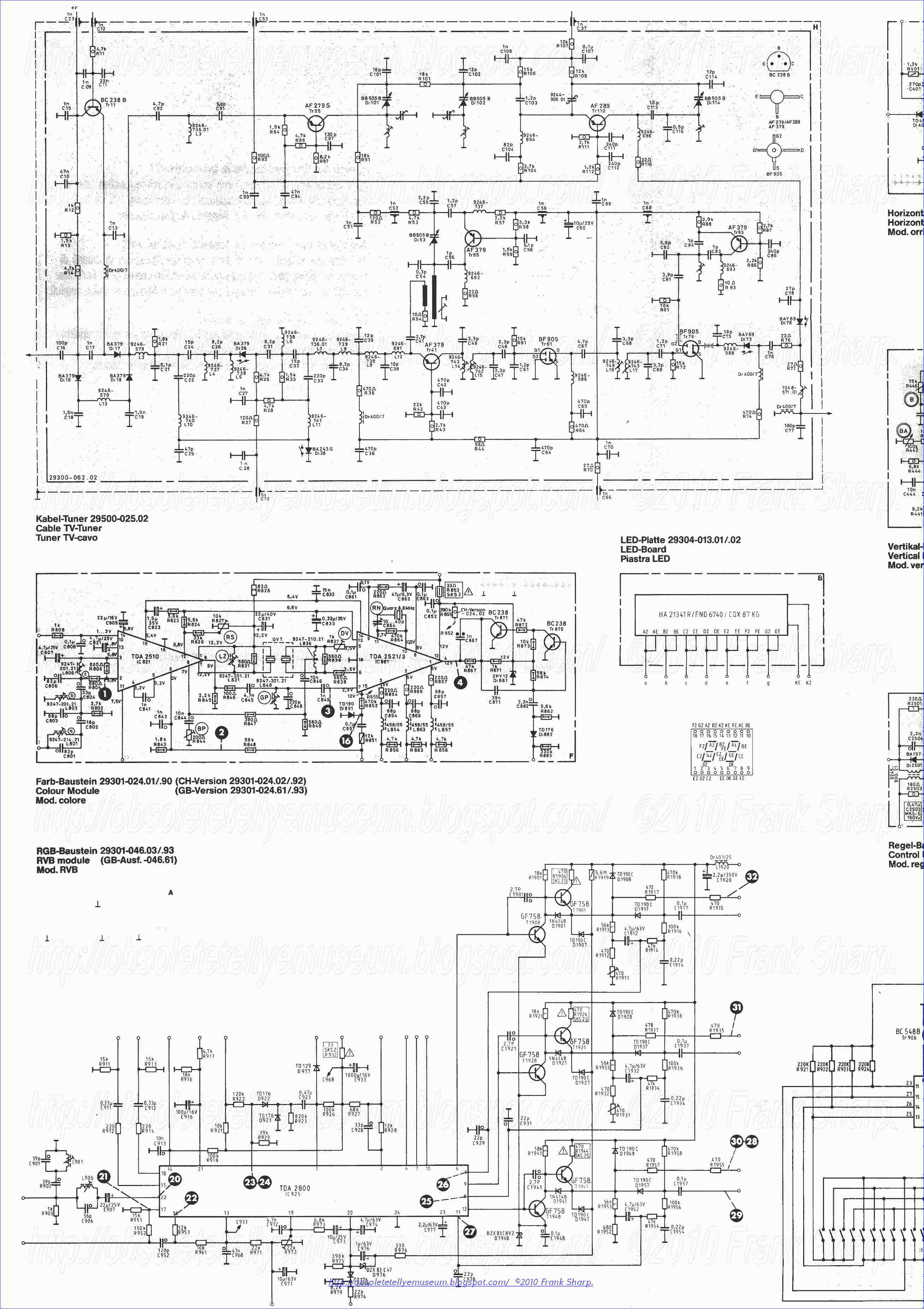
especially designed for use with this module should be used.The Tuner:
The tuner used is of the v.h.f./u.h.f. type, part no. 29500.
For many people, delving into tuners is taboo. If certain ground rules are observed however many common faults can be cleared. Tuning drift or failure to tune is caused by one of the varicap diodes going leaky. These diodes normally have a very high impedance and any leakage at all will cause drift. The best method of tracing this fault is to connect a sensitive d.c. meter, switched to 50µA, in series with the varicap control line, disconnecting each of the diodes in turn until the current returns to zero. Replace these diodes with the exact type - no substitutes.
The r.f. amplifier transistor Tr118 tends to go sick after a thunderstorm. To confirm this, inject a signal via a loop into the output tuning area - some sort of signal should then be evident.

RGB Module:
 The RGB module can present difficulties due to the feedback paths.
If a number of panels need repairing it's worth finding a good one and fitting a 24 -pin i.c. socket so that the TDA2800 i.c. can be proved before making further investigations. Most faults occur in the RGB output stages however.
Here are one or two odd faults: no luminance, C907 (22µF) or the delay line (on the main panel) open -circuit; no luminance and low brightness, C977 (2.2µF) leaky.
There are obviously many internal faults that could occur in the i.c., causing obscure symptoms. Some less common faults I've had on the module are as follows. R1919 open -circuit, no contrast control. Zener diode D1948 open -circuit or L1920 high -resistance, uncontrolla- ble brightness.
Other faults depend on which output stage is involved.
For the red output stage, R1904 open -circuit causes a tint of that colour on the background and loss of h.f. response; C1912 or C1914 leaky causes no red; R1911 open -circuit results in full beam current, as does T1908 going leaky or short-circuit; T1901 going short- circuit causes no colour. The relevant components in the blue and green output stages give analogoui faults.
Chroma Module:
Many chroma module
 faults
are due to the two i.c.s (TDA2510 and TDA2521). There seem to have been
difficulties with the TDA2521 as at least three versions were made, the
TDA2521/3 being the latest. If there's no colour, check the colour
burst level at pin 7 of IC861. It should be 0.5V peak -to -peak. Under
fault conditions it may rise to 2.5V p -p and not be controllable with
R827. Check C833 which could be leaky, IC861, and C823/832 which could
be open -circuit.
faults
are due to the two i.c.s (TDA2510 and TDA2521). There seem to have been
difficulties with the TDA2521 as at least three versions were made, the
TDA2521/3 being the latest. If there's no colour, check the colour
burst level at pin 7 of IC861. It should be 0.5V peak -to -peak. Under
fault conditions it may rise to 2.5V p -p and not be controllable with
R827. Check C833 which could be leaky, IC861, and C823/832 which could
be open -circuit.If there's still no colour, check the reference oscillator and its tuning.
As with the RGB module, if you've many panels to look after it's worth fitting i.c. sockets to a known good one for use as an i.c. test bed. If the R -Y or B -Y signals are missing, suspect IC861 and either L854 or L857 for being open - circuit. If R828 has burnt up, check whether C831 is short-circuit. Di881 (12V zener diode) leaky causes green flashing lines while C809 causes weak flashing colours.
As mentioned in a letter (June issue) C843 must be changed to 0.0047µF if you have a colour locking problem with the Sinclair Spectrum microcomputer. this post has shed light on the problems that can be encountered with the GSC100 chassis. Most of the comments also apply to the GSC200 chassis which differs in only minor respects from the GSC100 (vision i.f. module, tuning system and the inclusion of a relay board).
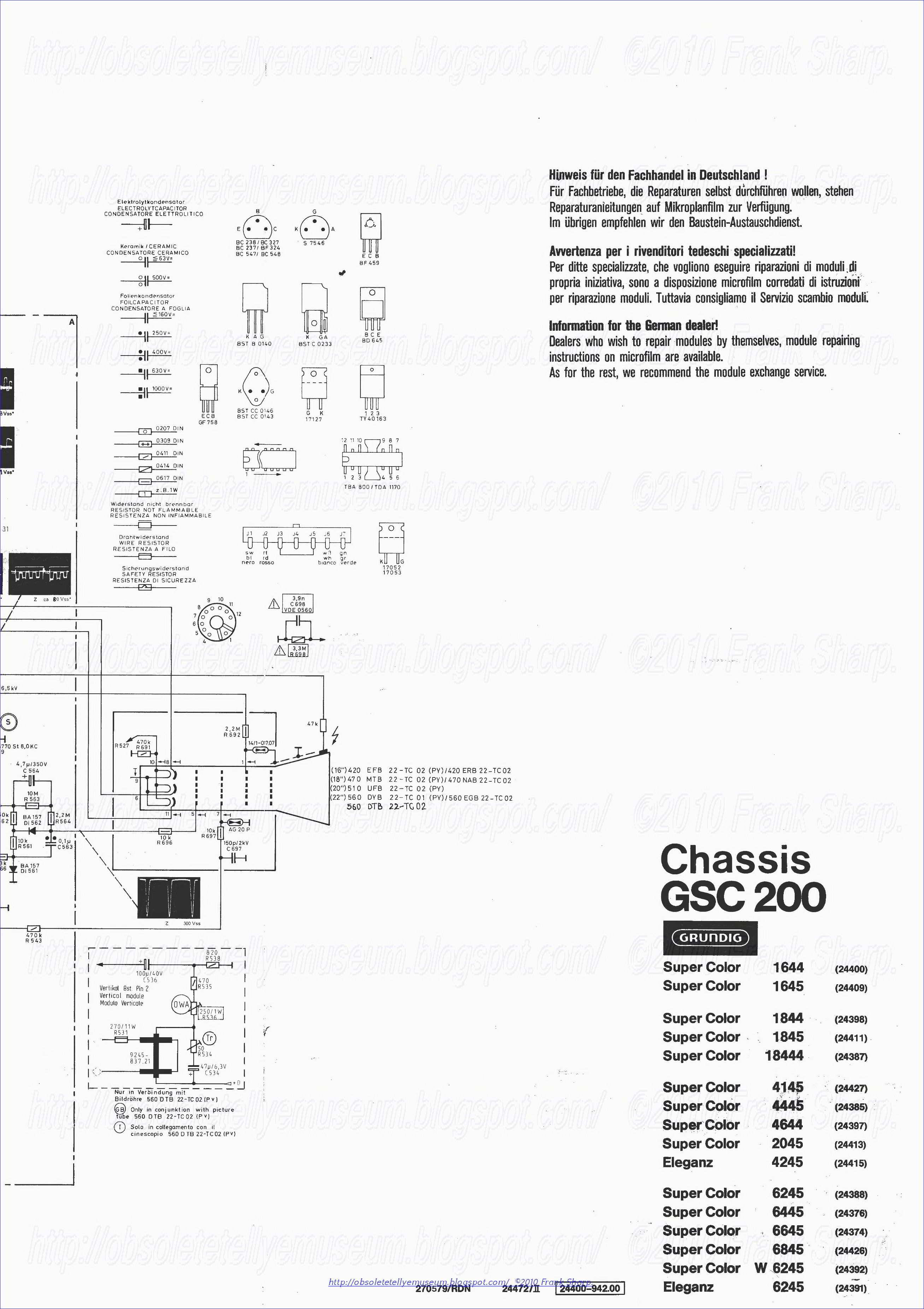
GRUNDIG SUPER COLOR 4644 SERIE 30F20 CHASSIS GSC200 (29304-178.01(12)) TUNING CONTROL SYSTEM (Abstimm Baustein 29502.003.22)


The Tuning system in this set is a voltage synthesized tuner controlled by a sophisticated
and complex unit called Abstimm Baustein 29502.003.22 (Tuning Unit) which features all the functions of the set
via ASIC ICs and a uC (Microcontroller) from Texas Instruments TMS1100. Additional ASICs TMS1100P1072B (Uc Masked) TMS 3755 . ICs SN29799N , 2x TMS3529nl (Channel Memory), TMS3731bnl SN29762N.

Tuning system in this set is a voltage synthesized tuner controlled by a sophisticated
and complex unit called Abstimm Baustein 29502.003.22 (Tuning Unit) which features all the functions of the set
via ASIC ICs and a uC (Microcontroller) from Texas Instruments TMS1100. Additional ASICs TMS1100P1072B (Uc Masked) TMS 3755 . ICs SN29799N , 2x TMS3529nl (Channel Memory), TMS3731bnl SN29762N.
TMS1000
General
General Information
Texas Instruments was locked in a race with Intel to create the first microprocessor. By most accounts Intel won with the 4004, but there are a few die hard TI fans who say the TMS1000 was first, because it was the first “computer on a chip” and that the 4004 was just a calculator chip.
Texas Instruments followed the Intel 8080 with the 4-bit TMS1000. So, while Intel was leading the industry in microprocessors, TI led with this industry unique design "a computer on a chip", specifically designed for control and automation purposes. The 1000 was the first MCU (MicroComputer Unit) , which is an MPU (MicroProcessor Unit) with other support chips (such as RAM, ROM, counters, timers, I/O interfaces) integrated on to the same silicon chip.
The original 1000 family consists of 6 chips the TMS1000 and TMS1200 are basic chips, the TMS1070 and TMS1270 are high voltage versions to interface to displays, the TMS1100 and TMS1300 provide twice the on-board ROM and RAM. The TMS1000, TMS1070, and TMS1100 are 28-lead packages, the TMS1200, TMS1270, and TMS1300 are 40-lead versions of the same chips (just 200 to the 28-lead chip numbers).
In the 80's TI added to the 1000 family. The 28-lead TMS1170 started with a TMS1100 base and added fluorescent display drive capability and expanded memory (2KB ROM). The TMS1370 was the same as the TMS1170 and added 27 I/O lines. An expanded memory group based on the original TMS1000 chips was also created. They were the TMS1400, TMS1470, and TMS1700 (64 Bytes RAM, 4KB ROM). There were 40-lead versions of the TMS1400 and TMS1470, which because the TMS1600 and TMS1670. CMOS versions were also added, denoted with a "C" suffix, such as TMS1200C.
The TMS1000 also had system evaluator chips. The original evaluator chips were the TMS1098 and TMS1099. These 64-lead evaluator chips were ROM-less versions of their corresponding standard chips. The TMS1099 supported the TMS1000/TMS1200 and the TMS1070/1270. The TMS1098 supported the TMS1100/1300. Later evaluators were introduced to support the entire TMS1000 family, they were the SE1000P (supports TMS1000,1070,1200,1700), SE2200P (supports TMS1100,1170,1300,1370), and the SE1400P (supports 1400, 1470, 1600, 1670).
The success of the the TMS1000 is demonstrated by its long lifecycle (over 20 years) and its expanded product line. The TMS1000 is found in many appliances, control systems, and games. Most of these chips were sourced by companies for direct use in their products and will have custom or house numbers on the chips (not the standard numbers listed above). Even TI used custom numbers in its products. The TMS1000 was used as a customized chip in the Texas Instruments "Speak and Spell" educational toy line (See Pictures at bottom).
Production
Early 1975.
GRUNDIG SUPER COLOR 4644 SERIE 30F20 CHASSIS GSC200 (29304-178.01(12)) Microcomputer processing approach for a non-volatile TV station memory tuning system:
A television tuning system having a non-volatile memory for storing
digital tune words is electrically updated by a microcomputer type
architecture control circuitry. A ROM memory matrix is provided for the
storage of VHF minimum and maximum binary tune words corresponding to
each of twelve VHF channels in addition to a UHF minimum and maximum
binary tune word encompassing all possible 72 UHF channels. Tuning of
individual VHF and UHF chanels is accomplished by incrementing or
decrementing a given tune word within the minimum and maximum limits
established in the ROM memory matrix by means of a microcomputer
processing approach.TMS1000 General
General Information:
Texas Instruments was locked in a race with Intel to create the first microprocessor. By most accounts Intel won with the 4004, but there are a few die hard TI fans who say the TMS1000 was first, because it was the first “computer on a chip” and that the 4004 was just a calculator chip.
Texas Instruments followed the Intel 8080 with the 4-bit TMS1000. So, while Intel was leading the industry in microprocessors, TI led with this industry unique design "a computer on a chip", specifically designed for control and automation purposes. The 1000 was the first MCU (MicroComputer Unit) , which is an MPU (MicroProcessor Unit) with other support chips (such as RAM, ROM, counters, timers, I/O interfaces) integrated on to the same silicon chip.
The original 1000 family consists of 6 chips the TMS1000 and TMS1200 are basic chips, the TMS1070 and TMS1270 are high voltage versions to interface to displays, the TMS1100 and TMS1300 provide twice the on-board ROM and RAM. The TMS1000, TMS1070, and TMS1100 are 28-lead packages, the TMS1200, TMS1270, and TMS1300 are 40-lead versions of the same chips (just 200 to the 28-lead chip numbers).
In the 80's TI added to the 1000 family. The 28-lead TMS1170 started with a TMS1100 base and added fluorescent display drive capability and expanded memory (2KB ROM). The TMS1370 was the same as the TMS1170 and added 27 I/O lines. An expanded memory group based on the original TMS1000 chips was also created. They were the TMS1400, TMS1470, and TMS1700 (64 Bytes RAM, 4KB ROM). There were 40-lead versions of the TMS1400 and TMS1470, which because the TMS1600 and TMS1670. CMOS versions were also added, denoted with a "C" suffix, such as TMS1200C.
The TMS1000 also had system evaluator chips. The original evaluator chips were the TMS1098 and TMS1099. These 64-lead evaluator chips were ROM-less versions of their corresponding standard chips. The TMS1099 supported the TMS1000/TMS1200 and the TMS1070/1270. The TMS1098 supported the TMS1100/1300. Later evaluators were introduced to support the entire TMS1000 family, they were the SE1000P (supports TMS1000,1070,1200,1700), SE2200P (supports TMS1100,1170,1300,1370), and the SE1400P (supports 1400, 1470, 1600, 1670).
The success of the the TMS1000 is demonstrated by its long lifecycle (over 20 years) and its expanded product line. The TMS1000 is found in many appliances, control systems, and games. Most of these chips were sourced by companies for direct use in their products and will have custom or house numbers on the chips (not the standard numbers listed above). Even TI used custom numbers in its products. The TMS1000 was used as a customized chip in the Texas Instruments "Speak and Spell" educational toy line (See Pictures at bottom).
1. A broadcast receiver tuning system for tuning said broadcast receiver to a selected frequency comprising:
first means for storing digital tune words responsive to a binary address for outputting a selected said digital tune word,
second means for storing said selected digital tune word and said binary address operably associated with said first means for storing,
a microcomputer operable for selectively changing said digital tune words in said first and second means for storing, and
means for converting said digital tune word stored in said second means for storing into an analog voltage operative to tune said broadcast receiver to said selected frequency.
2. A tuning system of claim 1 wher
ein said microcomputer comprises:
means for incrementing and decrementing said digital tune word stored
in said second means in updating said digital tune word, means for providing a plurality of operating instructions and logic functions operative of said microcomputer,
means for storing binary data responsive to said binary address and said instructions operative for incrementing and decrementing said digital tune word stored in said second means for storing, and
means for inputting control functions operably associated with said means for providing a plurality of operating instructions.
3. A tuning system of claim 1 wherein said means for converting comprises: a pulse width modulator generator for outputting a digital signal proportional to said digital tune word, and
a digital to analog converter for converting said digital signal into said analog voltage for tuning said broadcast receiver to said selected frequency.
4. A tuning system of claim 1 wherein said broadcast receiver comprises a television set.
5. A tuning system of claim 1 wherein said first means for storing digital tune words comprises a nonvolatile random access memory.
6. A tuning system of claim 1 wherein said second means for storing said digital tune word and said binary address comprises a shift register.
7. A tuning system of claim 2 wherein said means for incrementing and decrementing comprises an arithmetic logic unit.
8. A tuning system of claim 7 wherein said arit
hmetic logic unit comprises: a plurality of shift registers, a one bit full adder operably associated with said plurality of shift registers for adding and subtracting said digital tune words and said binary data stored in said plurality of shift registers, and
means for storing said digital tune words and said binary data operably associated with said plurality of shift registers and said one bit full adder.
9. A tuning system of claim 2 wherein said means for providing a plurality of operating instructions and logic functions comprises: a program counter,
an instruction memory responsive to said program counter for outputting binary instructions, and
a program logic array responsive to said binary instructions for outputting a plurality of said logic functions.
10. A tuning system of claim 9 further including a microprogram counter operably associated with said program counter.
11. A broadcast receiver tuning system for tuning said broadcast receiver to a selected frequency comprising: a first memory matrix
for storing digital tune words corresponding to said selected frequency, means for generating a binary address for addressing said digital tune word from said first memory,
means for storing said binary address and said addressed digital tune words operably associated with said first memory and said means for generating said binary address,
means connected to said address and tune word storing means for incrementing and decrementing said addressed digital tune word for updating said digital tune word,
means responsive to said binary address for outputting selected binary data from a second memory matrix, said binary data used for incrementing and decrementing said addressed digital tune word,
means connected to said incrementing and decrementing means for providing a plurality of operating instructions and logic functions operative for updating said digital tune word,
means for inputting control functions operably associated with said means for providing a plurality of operating instructions, and
means for converting said addressed digital tune word into an analog voltage operative to tune said broadcast receiver to said selected frequency.
12. A tuning system of claim 11 wherein said digital tune words further correspond to a plurality of VHF and UHF television channels.
13. A tuning system of claim 11 wherein said means for storing said binary address and said addressed digital tune word comprises a shift register.
14. A tuning system of claim 11 wherein said means for incrementing and decrementing comprises: a plurality of shift registers,
a one bit full adder operably associated with said plurality of shift registers for adding and subtracting said digital tune words and said binary data stored in said plurality of shift registers, and
means for storing said digital tune words and said binary data operably associated with said plurality of shift registers and said one bit full adder.
15. A tuning system of claim 11 wherein said means for providing a plurality of operating instructions and logic functions comprises: a program counter,
an instruction memory responsive to said program counter for outputting binary instructions, and
a program logic array responsive to said binary instructions for outputting a plurality of said logic functions.
16. A tuning system of claim 11 wherein said means for inputting logic control functions comprises an input logic
status
switch. 17. A tuning system of claim 11 wherein said means for converting comprises: a pulse width modulator generator for outputting a digital signal proportional to said digital tune word, and
a digital to analog converter for converting said digital signal into said analog voltage for tuning said broadcast receiver to said selected frequency.
18. A tuning system of claim 15 further including a microprogram counter operably associated with said program counter.
19. A tuning system of claim 14 further including an automatic channel shift encode for normalization of a binary VHF increment value comprising one of said binary data stored in said second memory matrix.
20. A television tuning system for tuning said television to a selected VHF and UHF channel comprising: a first memory matrix for storing digital tune words corresponding to said VHF and UHF channels,
means for generating a binary address on a multibus line for outputting said digital tune words from said first memory,
a shift register operably associated with said first memory and said
means for generating a binary address for storing said digital tune word
and said binary address, an arithmetic logic unit for incrementing and decrementing said digital tune word stored in said serial shift register in updating said digital tune word,
means for providing a plurality of operating instructions and logic functions operative in updating said digital tune word,
a second memory matrix for storing binary data used in incrementing and decrementing said digital tune word, said second memory matrix responsive to said binary address and said operating instructions, said second memory matrix also operably associated with said arithmetic logic unit,
an input logic status switch for inputting control functions operably associated with said means for providing a plurality of operating instructions,
a pulse width modulator responsive to said digital tune word stored in said shift register for outputting a digital signal proportional to said digital tune word, and
means for converting said digital signal to an analog voltage operative to tune said television to said selected UHF or VHF channel.
21. A tuning system of claim 20 further including an automatic channel shift encode for normalization of a binary VHF increment value comprising one of said binary data stored in said second memory matrix.
22. A tuning system of claim 20 wherein said means for providing a plurality of operating instructions and logic functions comprises: a program counter,
an instruction memory responsive to said program counter for outputting binary instructions, and
a program logic array responsive to said binary instructions for outputting a plurality of said logic functions.
23. A tuning system of claim 22 further including a microprogram counter operably associated with said program counter.
Description:
BACKGROUND OF THE INVENTION
This invention relates in general to the tuning of a broadcast receiver, and more particularly relates to the tuning of a television receiver using a non-volatile memory for storing binary tuning words that are electrically updated by a microcomputer type architecture control circuitry.
Previously developed electronic channel tuning systems have not been sufficiently flexible to enable wide-spread use for a variety of different types of television sets in applications. For example, certain previously developed systems have required extremely uniform varactor tuning diodes to enable channel tuning, thereby allowing insufficient tolerances for co nventional variances between
varactor diodes. Other previously developed systems have not been
sufficiently modular to enable a selection of various types of channel
access or displays. Moreover, previously developed electronic channel
tuning systems have not been sufficiently economical to fabricate and
have required uneconomical printed circuit boards or other uneconomical
fabrication techniques for construction. For example, certain prior
systems have required expensive potentiometers for each channel desired
to be tuned. In addition, previously developed electronic television
tuning systems have not satisfactorily satisfied recent regulatory
requirements which call for a television tuner to provide a comparable
capability and quality of tuning for both VHF and UHF stations.
Specifically, such prior tuning systems have not enabled selection of
precise UHF channels, nor have the prior systems provided means for
easily changing selected UHF channels.
nventional variances between
varactor diodes. Other previously developed systems have not been
sufficiently modular to enable a selection of various types of channel
access or displays. Moreover, previously developed electronic channel
tuning systems have not been sufficiently economical to fabricate and
have required uneconomical printed circuit boards or other uneconomical
fabrication techniques for construction. For example, certain prior
systems have required expensive potentiometers for each channel desired
to be tuned. In addition, previously developed electronic television
tuning systems have not satisfactorily satisfied recent regulatory
requirements which call for a television tuner to provide a comparable
capability and quality of tuning for both VHF and UHF stations.
Specifically, such prior tuning systems have not enabled selection of
precise UHF channels, nor have the prior systems provided means for
easily changing selected UHF channels.
A major disadvantage in the channel tuning sections of television receivers has been the inability to electronically program and store tune voltages under all operating and non-operating conditions without using an auxiliary power source or a mechanically programmed memory. Existing electronically operable tuners are dedicated electronic circuitry to program tune voltage information in volatile memories where the volatile memories require batteries to provide standby power when the main powe r source is
removed. The batteries are undesirable because they represent an
additional cost to the manufacturer and a present a long-term tune
voltage jeopardy if they fail when the main power source is removed.
Memory loss due to battery failure can occur if there are poor battery
connections, battery corrosion, or excessive battery drain. Other tuning
systems use potentiometers to retain the channel tune voltage, but are
also undesirable because they are not electronically alterable, and
require a potentiometer for each channel to be tuned.
r source is
removed. The batteries are undesirable because they represent an
additional cost to the manufacturer and a present a long-term tune
voltage jeopardy if they fail when the main power source is removed.
Memory loss due to battery failure can occur if there are poor battery
connections, battery corrosion, or excessive battery drain. Other tuning
systems use potentiometers to retain the channel tune voltage, but are
also undesirable because they are not electronically alterable, and
require a potentiometer for each channel to be tuned.
In accordance with the present invention, the undesirable characteristics are eliminated by using a non-volatile DIFMOS memory matrix to store the channel tune voltages. The DIFMOS memory (dual injection floating gate MOS technology) is electronically alterable and has a projected memory retention capability of over 100 years with power removed. The control circuitry for the system uses a microcomputer type architecture to integrate the user control inputs and to generate the signals needed to access and alter the DIFMOS memory matrix. A principal advantage of this type of control compared to the dedicated control circuit approach is the ease with which different manufacturers' system requirements can be satisfied by simply reprogramming the algorithm of the instruction memory.
Accordingly, an object of the present invention is to provide an electronically programmable television tuning system having a non-volatile memory matrix for the storage of binary tune words.
Another object of the present invention is to provide electronic alterable tuning means for a broadcast receiver using a microcomputer approach, thereby eliminating the need for dedicated control circuitry.
Yet another object of the present invention is to provide means for electronically updating binary tune words of a selected channel in the tuning of a television receiver and for storing the updated binary words in a non-volatile memory matrix.
Still a further object of the present invention is to provide a means for generating a binary tune word corresponding to a selected UHF or VHF channel within the limits of a binary minimum and maximum word stored in a memory matrix.
SUMMARY OF THE INVENTION
A television tuning system is taught having a non-volatile RAM memory for storing digital tune words that are electronically updated by a microcomputer type architecture control circuitry. A five-bit binary address word is provided for addressing a 15-bit binary word from a non-volatile memory matrix. The 15-bit binary word comprises 14 bits corresponding to a tune word for the channel selected and a 15th MSB as a skip toggle indicator. The 20 bits are stored in three shift registers in the data in/out circuit in a 5-bit address buffer, a 1-bit skip toggle buffer, and a 14-bit data buffer register. The 14-bit tune word is placed in a data latch comparator for the PWM generator. An analog circuit provides the voltage conversion of the digital output of the PWM generator proportional to the tune word for applying to the varactor tuner of the TV at a selected frequency.
The binary tune word is incremented or decremented to provide an updated tune word in tuning the system by means of a microcomputer approach. The binary tune word is written and read from the non-volatile memory by the same microcomputer system.
The 14-bit binary tune word is updated either by external user control or AFC tuning. In either mode of operation, the tune word is incremented or decremented within a minimum and maximum binary tune word that is stored in a ROM memory matrix. In addition, increment values and tuning time limits are also stored in the ROM memory matrix. An arithmetic logic unit comprising a temporary storage RAM file, two 14-bit working registers, anda 1-bit full adder provide the means for
performing the system's computations.
An 8-bit program counter provides the binary address of instructions in the 8 × 256 instruction ROM which addresses the PLA decode providing for an instruction generator. The PLA decode provides 26 "and" functions and 12 "or" functions. In addition, a 12 to 1 input logic status switch provides the necessary status indication for the 12 external controls. These input signals are detected by a 1-bit status latch.
The system is partitioned into two major functions: the non-volatile memory and the digital to analog converter and control circuits. The channel addressing and varactor diode band selection is generated with a rotary switch assembly. While a rotary switch assembly was used to implement the embodiment, non-volatile memory designs have been generated for addressing and band selection and could be easily implemented. The tune voltage interface between the digital to analog converter and the varactor diodes use standard oscillator and amplifier buffer circuits to provide the AFC summing and UHF tuning functions.
BRIEF DESCRIPTION OF THE DRAWINGS
The novel features believed characteristic of the invention are set forth in the appended claims. The invention itself, however, as well as further objects and advantages thereof, will best be understood by reference to the following detailed description of an illustrated embodiment taken in conjunction with the accompanying drawings, in which:
FIG. 1 is a functional block diagram employed to illustrate the present invention in a TV receiver.
FIGS. 2, 2A-2B are detailed circuit diagrams of the input buffer registers in the data in/out circuit.
FIGS. 3, 3A-3B are detailed circuit diagrams of the ROM constant file and its addressing circuitry.
FIG. 4 is a detailed circuit diagram of the automatic channel shift encode.
FIGS. 5, 5A-5D are detailed circuit diagrams of the instruction ROM, program counter, and microprogram counter.
FIGS. 6, 6A-6D are detailed circuit diagrams of the instruction PLA.
FIGS. 7, 7A-7B are detailed circuit diagrams of the input logic status switch.
FIGS. 8, 8A-8D are detailed circuit diagrams of the arithmetic logic unit.
FIGS. 9, 9A-9B are detailed circuit diagrams of the PWN generator.
FIGS. 10, 10A-10B are detailed circuit diagrams of the analog circuitry.
FIGS. 11A-11H are detailed architecture diagrams of the microcomputer system.
FIG. 12 represents the tune voltage amplifier diagram and related equations for calculating binary words corresponding to tune voltages.
FIGS. 13, 13A-13L are detailed drawings of the instruction set algorithm for the non-volatile stationary memory tuning system.
DETAILED DESCRIPTION
A more complete understanding of the detailed embodiment will be understood by a brief description of the requirements of the system. The fine tune up or down is accomplished by a rocker switch with center off position. A closed position on the switch will increment the tune voltage at the rate of 2 to 8 steps per second. The fine tune control is operative on VHF and UHF tuning modes.
UHF programming is accomplished by pushing a potentiometer control knob and turning the knob pointer to the desired channel number. When the knob is pushed, a contact is switched to ground. The knob is spring loaded in the out position and cannot be turned unless pushed in. The UHF programming potentiometer has approximately 30 turns. The user is able to fine tune a UHF station with this potentiometer and also with a fine tune rocker switch. The UHF fine tune limit is said to be plus or minus 128 steps from the binary word stored in the non-volatile memory RAM matrix only when the fine tune rocker switch is used. If the user continues to hold the rocker switch in the same mode after 128 steps, the tune voltage reverses direction and increments in the other direction for 256 steps until it hits the other limit where it reverses direction again.
Storage and memory requires approximately 240 milliseconds. The binary tune voltage word and skip signal is stored when the set is turned off. If any tuning control for the channel skip button has been engaged while addressing the channel, the tune voltage andskip will also be stored in
the memory when a channel change occurs.
An interchannel AFC defeat pulse occurs between each adjacent channel position. The pulse occurs when a switch contact is momentarily shorted to ground. The duty cycle of the pulse is approximately constant versus the rate of rotation of the channel select knob. The duty cycle is about 25% contact closed and 75% contact open. The binary input address is sampled and latched at the end of a write time or 48-68 milliseconds after receipt of the last interchannel pulse, whichever occurs last. A user programmable skip channel signal output is utilized. The operator uses a pushbutton to change the state of the signal.
The system has been designed for a 20 channel capacity. This includes 12 dedicated VHF channels plus 8 undedicated UHF channels. In VHF mode, a ROM plus non-volatile RAM approach is used to limit fine tuning. The ROM plus RAM make up a 14-bit tuning word plus a 1-bit skip flag. The RAM is 8-bits tuning word plus skip flag. The system is designed such that the LSB of the 8-bit tuning word can be reprogrammed for each VHF channel to occur anywhere from the LSB position to the 7th bit of the 14-bit tuning word. In the UHF mode the RAM shall be 14-bits for the tuning word plus 1 bit for skip flag.
 Referring
now to the block flow diagra
Referring
now to the block flow diagra
m of FIG. 1, the TV tuning microcomputer approach flow diagram is indicated. The television receiver 2 has a selector switch 26 for generating an address for the non-volatile memory matrix contained in the microprocessor circuitry 4. A more detailed block diagram of the non-volatile memory architecture and address architecture is indicated in FIG. 11A. In one embodiment the non-volatile memory comprises a DIFMOS memory matrix (dual injection floating gate metal oxide semiconductor). Data retention without power is achieved by storing charge on an array of floating gates. Any floating gate in the memory array can be charged or discharged by the injection of electrons or holes from an avalanche plasma formed in two special injector structures within each bit. Once a floating gate has been charged, it will stay charged almost forever, unless it is intentionally discharged by reprogramming. The decay rate of a charge from a floating gate has been measured at less than 1% of the initial value per decade of time at 85° C. In the embodiment described the Texas Instruments X-929A decoded 32 bit non-volatile RAM semiconductor memory is used. However, other non-volatile memories may additionally be used in the present invention.
 Digital tune words corresponding to the
UHF and VHF channels are read from the memory and written into the
memory by way of the data in/out circuitry. The data in/out circuitry
contains temporary storage registers for the 5 bit channel address, the 1
bit skip toggle indicator, and the 14 bit tune word. The tune word is
loaded into the PWM comparator where a PWM counter and PWM generator
produce digital output signals proportional to the binary tune word.
These digital output signals are fed to an analog circuit comprising an
op-amp for the conversion to the analog voltage required to be applied
to the varactor tuner of the television for tuning at the selected
channel.
Digital tune words corresponding to the
UHF and VHF channels are read from the memory and written into the
memory by way of the data in/out circuitry. The data in/out circuitry
contains temporary storage registers for the 5 bit channel address, the 1
bit skip toggle indicator, and the 14 bit tune word. The tune word is
loaded into the PWM comparator where a PWM counter and PWM generator
produce digital output signals proportional to the binary tune word.
These digital output signals are fed to an analog circuit comprising an
op-amp for the conversion to the analog voltage required to be applied
to the varactor tuner of the television for tuning at the selected
channel.
The channel shift encode is provided to normalize the bit weighting of the increment value for selected VHF channels. The normalized binary word is applied to the microprogram counter to provide shift controls to the various shift registers of the tuning circuitry in the VHF mode.
Input commands by the user is read into the system by means of the input logic and status latch. This provides a means of detecting a change of state on the input switches during a tuning function so that the system may be changed to the latest input command. The change of state is detected by a status latch which loads a new address of the instruction ROM into the program counter.
The program counter provides any one of 256 instruction addresses of the instruction ROM. The instruction ROM addresses the constant memory matrix which contains the upper and lower limits for the VHF and UHF channels, increment values for both VHF and UHF tuning, time increments, write time, and maximum times. In addition, the instruction ROM addresses the instruction PLA which contains decoding for 26 "and" functions and 12 "or" functions.
The ROM constant memory matrix transfers the data to the arithmetic logic unit which contains 2 working registers, a 1 bit full adder and a RAM temporary storage file. The arithmetic logic unit provides for the operation of incrementing and decrementing tune words, providing for write times, and time out functions. The new binary tune word from the arithmetic logic unit is loaded into the data in/out circuitry or read from it. In all aspects of the operation of the present invention, the binary tune word corresponding to the individually selected channel in both the VHF and UHF mode are stored in the non-volatile RAM memory matrix for addressing upon channel selection.


Referring now to FIGS. 2A-2B the data in/out circuitry comprising the input buffer registers is indicated in greater detail. A 5 bit address buffer serial register 230 is provided in addition to 2 D flip flops 232 and 254. A 3 to 1 encode 236 is provided for transmitting of data to the 14 bit input data buffer serial register 234A-234B. Data stored in the input data buffer is parallel loaded into the 14 bit data latch serial register 238A-238B the output of which is parallel loaded into a 14 bit pulse width modulated logic latch serial register. The D flip flop 232 provides as a 1 bit skip toggle buffer for the MSB of the tune word.
A more detailed circuit diagram of the address decode and ROM


constant file is indicated in FIGS. 3A-3B. Five bits from the address generator and 4 bits from the instruction ROM are decoded to address the 32 by 14 bit ROM constant file 264A-264B. The output of the ROM constant file is loaded into a 14 bit B working register.
 The automatic channel shift encode for
normalization in VHF tuning is indicated in greater detail by the
circuit diagram in FIG. 4. The 4 LSB's of output is applied to an encode
of the microprogram counter. Two serial shift registers 100 and 102 are
provided for transfer of data in the decode operation.
The automatic channel shift encode for
normalization in VHF tuning is indicated in greater detail by the
circuit diagram in FIG. 4. The 4 LSB's of output is applied to an encode
of the microprogram counter. Two serial shift registers 100 and 102 are
provided for transfer of data in the decode operation.
The instruction ROM, program counter, and microprogram counter circuitry are indicated in greater detail in FIGS. 5A-5D. The 8 by 256 bit instruction ROM 286A-286B is addressed by the 8 bit program counter 290A-290B. The 8 bit program counter is divided into two serial registers comprising 4 MSB's and 4 LSB's. The LSB's are loaded directly from the 8 bit instruction program word from the instruction ROM. The 4 MSB's are loaded into the program counter by means of the 4 bit page latch 294. In addition, 6 bits of the instruction program word are applied to a PLA decode and 4 LSB's of the instruction program word are applied to a 9 by 32 address decode of a ROM constant file. The 8 to 4 encode 302A and 302B is addressed by 4 LSB's from the 8 bit instruction word and 4 bits from an automatic channel shift encode. These 8 bits are encoded to 4 bits which addresses the 4 bit microprogram counter 400. Also, the 4 LSB's from the instruction ROM addresses a 4 to 12 decode for an input logic status switch. Two of the 4 LSB's addresses a 2 to 4 decode of a temporary storage RAM file in the arithmetic logic unit.

FIGS. 6A-6B is a more detailed circuit diagram of the instruction PLA. Six bits of address from the instruction ROM are used to address the 6 by 28 by 12 bit PLA decode. The output of the PLA comprise 26 "and" functions and 12 "or" functions.
 FIGS. 7A-7B is
a more detailed circuit diagram of the input logic status switch. The
12 inputs to the status switch are read by decoding 4 LSB's of
instruction word from an instruction ROM. An indication of a match
between the decode and the 1 of 12 inputs is indicated by the setting of
a status latch 282. This status latch is loaded to the one state in the
presence of any of the 12 input functions and a matching code.
FIGS. 7A-7B is
a more detailed circuit diagram of the input logic status switch. The
12 inputs to the status switch are read by decoding 4 LSB's of
instruction word from an instruction ROM. An indication of a match
between the decode and the 1 of 12 inputs is indicated by the setting of
a status latch 282. This status latch is loaded to the one state in the
presence of any of the 12 input functions and a matching code.

 FIGS.
8A-8D are a more detailed circuit diagram of the arithmetic logic unit
and temporary storage RAM file. The 14 bit word from a ROM constant file
is parallel loaded into the 14 bit B working serial register 274A-274B.
A 4 by 14 bit temporary storage RAM file 276A-276H is provided for
temporary storage of the data from the ROM constant file and working
registers. The temporary storage RAM file has four memory locations that
are selected by the 4 to 1 decode 308. Access to working register B is
by means of a 2 to 1 encode 304 and access to the 14 bit A working shift
register 266A-266B is by means of the 4 to 1 encode 270. The temporary
storage RAM file is accessed by means of the 3 to 1 encode 278. A 1 bit
full adder 288 is provided for addition and subtraction of the A and B
working registers. Two LSB's of instruction word are used to address the
temporary storage RAM file.
FIGS.
8A-8D are a more detailed circuit diagram of the arithmetic logic unit
and temporary storage RAM file. The 14 bit word from a ROM constant file
is parallel loaded into the 14 bit B working serial register 274A-274B.
A 4 by 14 bit temporary storage RAM file 276A-276H is provided for
temporary storage of the data from the ROM constant file and working
registers. The temporary storage RAM file has four memory locations that
are selected by the 4 to 1 decode 308. Access to working register B is
by means of a 2 to 1 encode 304 and access to the 14 bit A working shift
register 266A-266B is by means of the 4 to 1 encode 270. The temporary
storage RAM file is accessed by means of the 3 to 1 encode 278. A 1 bit
full adder 288 is provided for addition and subtraction of the A and B
working registers. Two LSB's of instruction word are used to address the
temporary storage RAM file.

 FIGS. 9A-9B is a more detailed circuit diagram of the pulse width modulator (PWM) generator. A 214
PWM counter 250A-250B is provided. The binary word output is parallel
loaded into a 14 bit PWM logic latch. When the 14 bit binary word from
the PWM counter matches the 14 bit tune word stored in the 14 bit data
latch the PWM logic latch is tripped and the PWM digital output is
generated.
FIGS. 9A-9B is a more detailed circuit diagram of the pulse width modulator (PWM) generator. A 214
PWM counter 250A-250B is provided. The binary word output is parallel
loaded into a 14 bit PWM logic latch. When the 14 bit binary word from
the PWM counter matches the 14 bit tune word stored in the 14 bit data
latch the PWM logic latch is tripped and the PWM digital output is
generated.


FIGS. 10A-10B are a more detailed circuit diagram of the analog circuit for converting the digital output of the PWM generator of an analog voltage to be applied to the varactor tuner of the television. In addition, circuits for PWM power up clear, AFC defeat, interchannel pulse, and UHF up/down circuitry are provided.
Referring now to the system diagram of FIGS. 11A-11H, the TV tuning
microprocessor architecture is indicated in greater detail than the
block diagram of FIG. 1. The 5 bit binary channel address is read off
the 20 position selector switch 202 by means of the address generator
204 in FIG. 11A. The binary address corresponds to any one of 20
channels, 12 of which are VHF channels and 8 of which are UHF channels.
In addition to the channel addressing the selector switch has means for
channel interrupt selection 224, means to select the varactor band of
the TV tuner 226, and means to program AFC bias on and off 228. The
channel address is read directly into the 5 bit address latch 206 in the
non-volatile RAM circuitry. Information in the 5 bit address latch 206
is used to address the 32 bit addressable non-volatile RAM matrix and
also provides a parallel input into a 5 bit address shift register 208.
The 5 bit address on a multibus line from the selector switch is used to
address one of the 20 locations in the non-volatile memory circuitry
used to retain the binary tune word. Provided in the memory circuitry
are 12 VHF binary tune words and 8 UHF binary tune words.

In series with the shift register 208 is a 15 bit data out shift register 210. These two shift registers 208 and 210 are in a read mode when not programmed to shift out. Therefore they are always looking at and reading the address latch 206 and the 15 bits of the memory matrix 212. Fourteen bits of the non-volatile RAM matrix are used for representing the binary tune word and the 15th MSB is used for a skip toggle indicator. The 20 bits comprising 5 from the address register and 15 bits from the data out register are serially shifted out when we read the non-volatile memory 212. As the bits are serially shifted out they are also fed back into the stack in a serial manner by loop 222 so that the 5 bit address and the 15 bit data tune word are restored into the registers.
The address and data tune word as they are shifted out of the registers into the control chip are fed into a 20 bit input data buffer comprising a 5 bit address buffer 230, a 1 bit skip toggle buffer 232, and a 14 bit input data buffer register 234 indicated
 in
FIG. 11B. The address buffer register 230 contains the last bits shifted
out of the non-volatile memory block which comprises the 5 address
bits. The 6th MSB is the skip toggle bit and resides in the skip toggle
buffer register 232 immediately following the address buffer. The 14 bit
data tune word is steered through a selector switch encode 236 into the
14 bit input data buffer register 234. The selector switch encode 236
has 3 select states comprising load input data buffer (LIDB), read
non-volatile memory (RNVM), and read input data buffer (RIDB). The 14
bit tune word is loaded into the data buffer register 234 by selecting
the read non-volatile memory mode of the selector switch encode 236.
in
FIG. 11B. The address buffer register 230 contains the last bits shifted
out of the non-volatile memory block which comprises the 5 address
bits. The 6th MSB is the skip toggle bit and resides in the skip toggle
buffer register 232 immediately following the address buffer. The 14 bit
data tune word is steered through a selector switch encode 236 into the
14 bit input data buffer register 234. The selector switch encode 236
has 3 select states comprising load input data buffer (LIDB), read
non-volatile memory (RNVM), and read input data buffer (RIDB). The 14
bit tune word is loaded into the data buffer register 234 by selecting
the read non-volatile memory mode of the selector switch encode 236.
The binary tune word in data buffer register 234 is loaded parallel into the 14 bit PWM logic latch 248 when there is a load PWM (LPWM) signal on the 14 bit data latch 238. The 14 bit tune word in the PWM logic latch 248 is used as a compare word for the 14 bit pulse width modulator counter 250. The pulse width modulator operates with a 1 MHz input clock from the PWM buffer and oscillator 252 that is fed into the 214 PWM counter 250 and runs continuously.
The
PWM counter 250 counts from binary 0 in a binary manner until it
reaches one of two conditions. First, if the binary word of the counter
250 compares with the 14 bit tune word in the PWM logic latch 248 then
the PWM logic latch which is performing a magnitude compare will provide
an output signal and trip a flipflop which will then remain in that
state until the counter completes its count-out cycle. The second
condition is when the PWM logic latch 248 is at an all 1 state whereby
the PWM counter would count up to an all 1 state that also corresponds
to the runover point of the counter. Therefore, the PWM counter will
always count up to 214 and then run over where 214 and a 1 MHz input corresponds to a writeout at 16 milliseconds.
In the PWM generator we therefore have a magnitude compare of the PWM counter with the 14 bit tune word stored in the 14 bit PWM logic latch 248 and when the first time there is a match of the counter and the binary magnitude we receive an output signal from the PWM logic latch 248 proportional to the tune word. To tune the television we alter the pulse width modulated signal from the PWM logic latch 248. We alter the pulse width modulated signal by changing the bit value of the binary tune word contained in the PWM logic latch thereby giving us a modulated pulse width at a duty cycle of 16 milliseconds.
The skip toggle bit in the skip toggle buffer register 232 may be altered by means of the skip toggle inputs through the MAND gate 256. In the program algorithm when the skip toggle is altered we read the information out and write it into memory once the function is complete. Altering of the skip toggle information is achieved by first reading the state of the skip toggle buffer 232 which contains an MSB that was read out of memory, loading that bit into a D register 254, and changing that information if we have a program input to change the state of the skip toggle. A skip toggle output 258 is provided to give an indication that the skip toggle has been altered and the present program condition of the skip toggle. The skip toggle is not applicable to a mechanical rotary type selector switch system as indicated in this embodiment whereas the selector switch 202 is of a rotary type. However, by replacing the rotary selector switch with an electronically addressable circuit as disclosed in U.S. Pat. No. 3,968,443 issued on July 16, 1976, assigned to Texas Instruments Incorporated, the same assignee of the present patent application, then a skip function would be applicable in the present tuning circuitry.
After loading the address buffer 230 with the 5 bits of address from the address generator 204 these 5 address bits are transferred in a parallel mode to the 9 by 32 address decode 260 and the 5 to 4

automatic channel shift encode (VHF only) 262 indicated in FIG. 11C. The automatic channel shift encode is used to determine whether the system is functioning in the UHF or VHF mode. If the system is functioning in the VHF mode the automatic channel shift encode provides one of four possible codes for incrementing the VHF tune word. The four codes corresponding to the particular incrementing bit value that applies to the VHF channel that has been selected by the address generator 204. Since there are only four increment rate values and 12 VHF tune words, the encode 262 selects depending upon which channel the system is on one of the four incrementing rate values to be applied to the given tune word.
The 5 bit address from the address buffer 230 is also parallel applied to the 9 by 32 address decoder 260 to select a 14 bit data word stored in the ROM constant file 264. The 5 bit address which determines the VHF or UHF channel is decoded by the 9 by 32 address decoder into a 32 bit address word to address the 32 by 14 ROM constant file. The four LSB's of the instruction code determines which of the 32 words we are addressing. These 32 fourteen bit words in the ROM constant file comprise upper and lower limits for the VHF channels, UHF channel limits, increment values for both VHF and UHF tuning, time increments, maximum times, and write time.
When we have read a tune word into the input data buffer 234 and want to perform a tuning function upon it, we transfer the 14 bits of data out of the input data buffer register and into the 14 bit A working register 266 by means of a read input data buffer (RIBD) command at the 4 to 1 encode switch 270. Also, the 14 bit word is serially transferred back into itself by means of loop 272. After loading register A with the 14 bit tune word, the tune limit and increment value is outputted from the 14 bit ROM constant file and loaded into the 14 bit B working register 274. These values are now loaded into the temporary storage RAM file 276 by selection of the LBMX command on the selector switch encode 278. The temporary storage file comprises a 4 by 14 bit RAM file. Tuning is now performed by adding an increment value which is stored in register B to the 14 bit tune word stored in register A if the system is in a tuned upmode and subtracting them if the system is in a tuned downmode.

The incremented or decremented tune word is restored into the A working register by means of the "A" normalize command on the selector switch encode 270 indicated in FIG. 11D.
After the restore operation the updated 14 bit tune word is transferred into the input data buffer 234 by performing a load input data buffer (LIDB) command on selector switch encode 236. The updated tune word is now stored into the input data buffer and also restored into register A. The updated tune word is now loaded into the 14 bit PWM logic latch 248 whereby the PWM counter 250 can compare its out to updated tune word.
Whenever a tuning function is performed the system goes through a sequence whereby it performs an addition and a time out routine in the arithmetic logic unit by decrementing our timing word until a negative number is reached. In each case information is read from the ROM constant file and stored into the temporary storage RAM file. This information is a function of the particular channel and whether the channel is a UHF or VHF channel. In the sequence the system always goes through reading the input switches so if there is a change of state on our input switches during a tuning function it will be detected and the system function will be changed to the latest input command.

These input control functions are read into the system by means of the 12 to 1 input logic status switch 280 having 12 inputs indicated in FIG. 11F. A 61 kilohertz slow clock is provided to perform the write function which in the case of the non-volatile memory comprising DIFMOS memory cells takes in the order of 100 milliseconds to write a 0 into the memory, therefore requiring a clock running at a slower rate then the control or processing clock that is normally used. The slow clock is also used to provide dampening when in the power up mode or after we have already completed a write command in writing into memory so that the system doesn't read the new word while it is still settling.
Another input is the UHF/VHF control line that is a function of the particular address that has been detected from our selector switch 202. A third and fourth input is an AFC high and an AFC low select. The function of the AFC high/low is to provide a digital AFC control function. The means of achieving the digital AFC control is not indicated in the figures or represented in the algorithm. However, the digital AFC control system could be incorporated into the architecture by means of a couple of comparator windows and the appropriate addition of control logic to the present algorithm.
A fifth input is a UHF up/down control that is a control from a comparator 282 that determines whether the tune voltage is above or below the corresponding potentiometer setting of the UHF channel coarse tune potentiometer 284. An additional input is a power on/off select. Upon a power down input the 14 bit tune word stored in the input data buffer register 234 is written into the addressable non-volatile memory.
The seventh input is a skip toggle input which is not incorporated into the present system. This skip function if made available would allow for the skipping over of selected channels but is not applicable to a mechanical rotary switch as noted above.
The eighth and ninth inputs comprise the rocker arm fine tuneup and fine tunedown for the control voltage. The UHF tune on/off control places the tuning function into a coarse UHF tuning mode. The AFC on/off switch is used to activate the
internal AFC tuning function or to allow for the external manual tuning
mode. The final switch on the input logic status switch is the
interchannel pulse that is inputted from the selector switch 202 by
means of the channel interrupt line 224. The interchannel pulse provides
an indication that the selector switch is in between channels in a
changing mode and also detects the completed change.
The twelve inputs are read into the input logic status switch. If one of the twelve logic status switches is activated it is compared with a particular select code and if there is any indication of a match on the read command of that given instruction to the particular switch being closed or opened as the case may be, the status latch flip-flop 282 is set. The status switch inputs are decoded by the 4 to 12 decoder 284 which is addressed by four LSB's of instruction from the instruction ROM 286. The status latch 282 provides an indication that the system has received an input corresponding to one that has been coded in the instruction table of the decoder 284.
The second input to the status latch 282 is the carry input from the one bit full adder when the system is in a subtract routine and if the subtract routine results in a negative number. The negative number indication is used to perform compare tests to determine whether an upper or lower tuning limit or timing limit has been reached. The setting of the status latch 282 provides an input to the instruction ROM 286 to load the program counter with a new page of instruction address.

The eight bit program counter 290 indicated in FIG. 11C receives its count clock input from the 250 kilohertz clock 292 which is a one quarter division of the one megahertz clock from the PWM counter 250. The program counter gives any one of 256 instruction addresses for the instruction ROM 286. The location of the program counter in its counting sequence may be altered by loading in a new eight bit word into the program counter. The four LSB's from the instruction ROM are parallel loaded into the four LSB positions of the eight bit program counter and parallel loaded into a four bit page batch 294. If the status latch is set by a subtract operation from reading an input from the logic status switch, then upon a load page command (LPD) applied to the NAND gate 296 the four LSB bits of address with be loaded from the page latch into the program counter in the MSB position.
The output of the instruction ROM 286 feeds into the instruction PLA circuitry 298 which outputs 26
 "and" functions and 12 "or"
functions indicated in FIG. 11E. The instruction PLA decode comprises
the 6 by 28 by 12 bit memory. These "and" and "or" functions correspond
to the instruction set that is used to program the system.
"and" functions and 12 "or"
functions indicated in FIG. 11E. The instruction PLA decode comprises
the 6 by 28 by 12 bit memory. These "and" and "or" functions correspond
to the instruction set that is used to program the system.
The four bit microprogram counter 300 is used to provide shift controls to the various shift registers of the tuning circuitry. And more particular, the microprogram counter allows for the shifting of the 14 bit data word in working register A into the input data buffer register. In addition it allows for the addition and subtraction of working registers A and B and also allows for the transfer of data to the non-volatile memory.
The maximum number of serial shifting by the microprogram counter is 14 bits. When the shifting produced by the microprogram counter is completed, the system operation is returned to the eight bit program counter where it is indexed to the next address in the program. The eight bit microprogram instruction is selected by the microprogram address select encode 302. Four bits from the automatic channel shift encode 262 and four LSB's from the instruction ROM are loaded parallel into the address select encode to provide four bits of instruction address for the microprogram counter 300.

Referring to FIG. 11D a switch encode 304 is provided to allow for a restore operation whereby the 14 bit word in the B working register is shifted back into itself. In addition the switch encode provides for a shifting of the 14 bit word from the temporary storage RAM file 276 into the working register. Switch encode 270 allows for the shifting of a 14 bit word into the A working register from the temporary storage RAM file, the input data buffer register 234, a sum product from the addition of working register A and register B by means of the one bit full adder 288, and finally the restore of the word in the A register into itself.
The temporary storage RAM file 276 is addressed by two bits from the instruction ROM through a 2 to 4 encode 306. The four bit word from the encode is used to select one of four 14 bit storage files in the RAM file 276 by means of the 4 to 1 selector encode 308.
The pulse width modulated output 310 from the PWM logic latch is fed into the PWM buffer 252.

The PWM signal from the PWM buffer is fed into a driver buffer 312 that is referenced to +5 volts in FIG. 11H. The PWM output continues through a three stage PWM filter to provide the IC filtering required for the resolution and ripple voltage needed for a pulse width modulated signal of the longest duration to an acceptable level in the UHF mode. The VHF mode would not need as much filtering to generate a PWM at an acceptable ripple level. However, at least three stages are required for UHF filtering.
The output of the three stage filter is a DC voltage that is proportional to the pulse width modulated signal, the pulse width modulated signal being proportional to the 14 bit tune word that has been loaded into the 14 bit input data buffer register and PWM logic latch. The tune voltage is amplified by inverting voltage amplifier 316 and subsequently filtered by an additional single stage filter 318. The final DC analog tune voltage is passed to the television varactor tuner for tuning to the selected channel.
A second comparator 282 comprises a UHF up/down comparator which receives its inputs from the three stage PWM filter and a UHF course tune potentiometer 284. The potentiometer is referenced to the same +5 volts as the driver buffer 212. The comparator 282 provides an indication as to whether or not the system is in the coarse tune mode of UHF, whether or not the system is above or below the desired tune voltage for the particular channel setting, and provides a coarse tuning signal for the controller.
FIG. 320 represents the power supply required for the operation of the tuning system. The +5 volts used to provide the upper
voltage for the tuning amplifier for the varactor tune voltage output.
The +17 volts is used for biasing of the MOS circuitry of the
non-volatile memory. The +10 volts is used for biasing the CMOS logic in
the system. The +5 volts is used for the TTL and I2 L logic
in the system. Finally, the 0 to -35 switch voltage is used for
programming the non-volatile memory when the system is in a write mode.
In performing a tuning function using the microcomputer approach in the VHF mode a binary tune word that is stored in the input data buffer register is incremented or decremented within the limits for the minimum and maximum tune voltages for the selected channel that is stored in the ROM constant file. The ROM constant file contains a binary word for the maximum tune voltage and minimum tune voltage for each of the 12 VHF channels. These limits establish the range of tuning permitted by the system. These values are individually selected for each of the VHF channels. In a similar manner minimum and maximum limits are established for the UHF channel. However, due to the large number of UHF channels the minimum and maximum limit are established so as to encompass all 72 UHF channels with tuning for the selected UHF channel falling therebetween.
Referring now to FIG. 12 the schematic diagram used for calculating the minimum and maximum tune voltages is indicated in addition to the equations used. Equation 3 is the input voltage as a function of the output tune voltage. Given the desired tune voltage EO the input voltage Ei may be calculated. In addition, by using equation 4 the bits corresponding to the input voltage is calculated thereby resulting in the binary tune word corresponding to the calculated input voltage.
In this regard, Table I indicates the VHF ROM constants for the minimum limits as established by equations 3 and 4. Each of the VHF channels have a unique binary word corresponding to the minimum voltage limit. In a similar manner Table II indicates the VHF ROM constant for the maximum tune voltage. As noted the nominal tune voltage for tuning the television will lie somewhere between these two established limits. The binary words comprise 14 data bits and are addressed by the 5 bit binary address from the selector switch.
The data including the VHF minimum and maximum limits are stored in the ROM constant file as indicated in Table III. As noted the ROM constant file has 32 separate data values stored therein. The VHF and UHF increment values are also stored in the ROM constant file. The maximum time for both VHF tuning and UHF tuning are also stored therein. In addition, the time increment value is also stored. Finally, the UHF minimum tune word and the UHF maximum tune word including the write time is stored in the ROM constant file.
Table IV indicates the PLA logic for automatic right shift addressing (VHF only) of the microprogram counter. As noted from Table III the VHF increment value has a 1 in the 7th bit position. During the incrementing or decrementing of the VHF word it is desired to increment or decrement at a particular bit weight value unique to each of the VHF channels. To accomplish this, the automatic channel shift encode provides for right shifting of the increments value so as to normalize it to provide a different bit weight for each of the 12 UHF channels. The number of right shift in the VHF mode for each of the selected channels is indicated in Table IV in addition to the encode word for the microprogram counter preset. Since the UHF tuning is performed by a process which provides for the increasing of the bit weight of the increment value, the normalization by right shifting the increment value is not needed.
The instructional logic from the PLA decode is indicated in Tables V and VI. In Table V the instruction ROM decode outputs comprising 12 NOR gate outputs is indicated. These 12 outputs provide the "OR" logic functions for the microcomputer program. Table VI indicates the 28 instruction ROM decode outputs of the PLA decode. These outputs comprise 28 "AND" logic functions for the microcomputer programming.
TABLE V
INSTRUCTION
ROM DECODE OUTPUTS
(NOR GATE OUTPUTS)
1. lpc = ubrn + brn s/l
2. μpc enable = rnvm + lnvm + rsax + rsbx + add + suba + subb + rmxa + rmxb + lamx + lbmx + nora + norb + resa + resb + ridb + lidb + wro + wri + 27 bit (of p.c.)
3. ld μpc = rnvm + lnvm + rsax + rsbx + nora + norb + resa + resb
4. data in sel idb = shift cont. in code = rnvm + lnvm
5. shift cont. idb = ridb + rnvm + lnvm + lidb
6. shift cont. ram = rmxa + rmxb + lamx + lbmx
7. ram data restore sel = rmxa + rmxb
8. shift cont. reg a = rmxa + lamx + rsax + add + suba + subb + nora + resa
9. reg a sel restore a = resa + lamx + lidb
10. reg a sel Σ = add + suba + subb
11. shift cont. reg b = rmxb + lbmx + rsbx + add + suba + subb + norb + resb
12. reg b sel restore b = resb + lbmx
table vi
instruction
rom decode outputs
(nand gate outputs)
0. unconditional branch (ubrn)
a. if s/l = 1 or 0 (i.e. DON'T CARE)
1. parallel loads program counter on clk with contents of page latch and 4 lsb's of ubrn code.
2. clears s/l on clk
1. branch (brn)
a. if s/l = 1
1. parallel loads program counter on clk with contents of page latch and 4 lsb's of brn code.
2. clears s/l on clk
b. if s/l = 0
1. do nothing
2. load page (ldp)
a. load 4 bit address code into page latch (4 msb's of address).
3. read rom (rrom)
a. parallel loads reg. b with contents of rom stored at location defined by 4 bit address code and/or channel select code (if vhf).
4. read inputs (rin)
a. enables input defined by 4 bit address to be gates thru to the s/l flip/flop. if input is "0" then s/l is loaded with a "1" on clk. if input is a "1" then s/l is loaded with a "0" on clk.
5. read channel code sw. (rccs)
a. sets input strobe to a "1" level so that the channel select switch can be parallel loaded into the nvm latch buffer on the memory ic.
6. load pwm (lpwm)
a. parallel loads the contents of the input data buffer register into the pwm data register during clk.
7. sense nvm (snvm)
a. sets sense line to "0" so that the contents of the nvm can be parallel loaded into the data buffer registers on the memory ic during clk.
***the following functions enable the μ program counter***
8. read nvm buffer (rnvm)
a. selects 4 bit address code to be loaded into μ program counter.
b. loads 4 bit address (0101) into μ program counter to reset it for 10 right shift functions. load occurs during clk.
c. on clk the program counter is disabled, and the μ program counter is enabled.
d. a right shift command is provided for the input buffer registers and the nvm buffer registers until the μ program counter reaches the 1111 state (10 shifts).
e. when the μpc is 1111 then on the next clock pulse (which sets the μpc to 0000) the clk input to the μpc is disabled, and the clk input to the program counter is restored.
f. note: this command sets the data select line to the memory ic to a logic "1" level, so that data can be sequenced out of the ic into the dac.
9. load nvm buffer (lnvm)
a. same as read nvm buffer except sequence (f) is: note: this command sets the data select line to the memory ic to a logic "0" level, so data can be sequenced into the memory ic from the dac ic.
10. right shift a (r.s.a. x)
11. right shift b (r.s.b. x)
a. selects 4 bit variable address code to be loaded into μ program counter.
b. loads μ program counter during clk.
c. disables program counter on clk.
d. enables μ program counter on clk.
e. enables data shift in (a) or (b) register. data in register (a) or (b) is with leading zero's during μ program count time then right shifted according to the following shift code.
f. when μpc is 1111 THEN ON NEXT CLK PULSE THE μPC CLK INPUT IS DISABLED AND THE PC CLK IS ENABLED.
12-1 add (a & b) (add)
a. program counter is disabled on clk.
b. μpc is enabled on clk.
c. shift controls to reg. a and reg. b are enabled.
d. reg. b restore sel. is enabled.
e. reg a Σ input select is enabled.
f. when μpc is 1111 THE μPC CLK IS DISABLED AND THE PC IS ENABLED.
12-2,3 subtract (b-a) (suba) subtract (a-b) (subb)
a. enables inverter input to adder (e) from reg. a or reg. b.
b. sets carry bit in e1 to "1".
c. pc is disabled on clk.
d. μpc is enabled on clk.
e. reg a and reg b shift control is enabled.
f. data is shifted serially from reg a and reg b into Σ.
g. data in reg b is restored into reg b without change.
h. Σ data out is stored in reg a.
i. when μpc is 1111 THEN PC IS ENABLED AND μPC IS DISABLED.
13-1 read ram ➝ a (rmxa)
read ram ➝ b (rmxb)
a. address bits (2 bits) select ram storage location.
b. control enables ram read storage gate.
c. control enabled ram ➝ a or ram ➝ b select.
d. pc is disabled on clk.
e. μpc is enables on clk.
f. ram & reg a or reg b shift gates are enabled.
g. data is shifted from ram to reg a or b until μpc is 1111 then μpc clk is disabled and pc clk is enabled.
13-3 load a ➝ ram (lamx) 1,2,3,4
load b ➝ ram (lbmx) 1,2,3,4
a. program counter is disabled on clk.
b. μpc is enabled on clk.
c. address bits (2 bits) select ram storage location.
d. shift controls for selected memory location are enabled.
e. reg a ➝ m sel. and REG A DATA RESTORE.
14-1 normalize a (nora)
14-2 normalize b (norb)
a. selects 4 bit channel encode address to be loaded into μpc (normalized code).
b. loads 4 bit channel encode address into μpc during clk.
c. pc is disabled on clk.
d. μpc is enabled on clk.
e. control enable shift gates of reg. a or b.
f. control sets reg. a and reg. b inputs (serial) to "0".
g. data is shifted in reg. a or b until μpc is 1111 then μpc clk is disabled & pc clk is enabled.
14-3 unused code
14-4 slow clock enable (sloc) switches the clock input to the μpc from t1 clock line to the slow clk line (16ms PERIOD).
15-1 read input data buffer (ridb)
a. enables buffer data select into reg a.
b. enables input buffer data restore select gate into data buffer.
c. enables input data buffer and reg. a data shift control.
d. pc is disabled on clk.
e. μpc is enabled on clk.
f. data is shifted from data buffer into reg. a until μpc is 1111, μpc is disabled and pc is enabled.
15-2 load input data buffer (lidb)
a. enables reg. a data select gate into data buffer reg.
b. enables restore select gate into reg. a.
c. control enables reg. a and INPUT DATA BUFFER SHIFT GATE.
D. pc is disabled on clk.
e. μpc is enabled on clk.
f. data is shifted from reg. a to data buffer until μpc is 1111, then μpc is disabled and pc is enabled.
15-3 clear write (cwro) resets the sense line to the memory ic to a "1"; switching the memory cells from a write mode to a read mode.
15-4 write (wro) sets the sense line to "0" on clk; thereby permitting data to be written into the memory ic cells.
15-5 dummy (unused) unused code used for dummy operations.
the op-codes for the single clock instructions including their address are indicated in Table VII.
The 4 bit and 6 bit op-codes for the microprogram control instructions including their addresses are indicated in Table VII.
The input control line read codes are indicated in Table IX. The input functions each have the same 4 MSB's (0100) and differ only in the 4 LSB's.
The ROM constant address codes are indicated in Table X. It is to be noted that the 12 VHF channels are encoded to 12 minimum limits and 12 maximum limits and use the first 24 ROM addresses (00000 to 10111). The remaining 8 words are located in the last 8 ROM addresses (11000 to 11111), thus using a 32 word by 14 bit ROM structure. A greater understanding of the tuning system and the information contained in Tables I-X is gained by referring to the instructions set algorithm.


 The
instruction set algorithm for the nonvolatile station memory tuning
system as indicated in FIGS. 13A-13L. The algorithm can be divided into a
series of four operating modes. The first operating mode comprises the
non-tuning mode, FIGS. 13A-13C, the second mode is the start of the AFC
off loop which comprises the tuning mode select and initialization FIGS.
13D-13F, the third mode comprises the start of the
The
instruction set algorithm for the nonvolatile station memory tuning
system as indicated in FIGS. 13A-13L. The algorithm can be divided into a
series of four operating modes. The first operating mode comprises the
non-tuning mode, FIGS. 13A-13C, the second mode is the start of the AFC
off loop which comprises the tuning mode select and initialization FIGS.
13D-13F, the third mode comprises the start of the

Rocker Tune loop that is the channel fine tuning mode FIGS. 13G-13H, and the fourth loop is the UHF Pot Tune loop comprising the UHF coarse tuning mode FIGS. 13I-13L.

The tuning system is activated by a power up entry 1 in FIG. 13A followed by a load page command (LDP) where a 4 bit address code is loaded into the page latch 294 to address one of the 16 pages in the instruction ROM 286. A clear write (SWRO) operation is performed to reset the sense line to the memory IC to switch the memory cells from a write mode to a read mode. A read channel interrupt loop is performed whereby the system reads the channel interrupt switch until the channel interrupt indication is no longer present.


A channel interrupt indication 224 from the selector switch 202 is applied to the input logic status switch 280. When the input signal matches a 12 bit binary decode 284 the status latch 282 is set. The read channel interrupt loop continuously reads the status latch to determine whether or not it has been set. As long as the status latch has been set from an indication of a channel interrupt the system will loop back into the read mode and will continue until the signal in the status latch is eliminated by the completion of a channel selection at the selector switch 202. The purpose of the channel interrupt read operation is to prevent the system from reading the channel tune word when the selector switch is being changed from one channel to another.
Upon jumping out of the read channel interrupt loop a read channel code switch (RCCS) is performed whereby the five bit address from the selector switch and address generator is parallel loaded into the nonvolatile memory address latch buffer 206 of the memory IC. A slow clock enable signal provides dampening to offset any electromechanical bouncing that may occur during the switching operation. Additional dampening is provided by right shift of the B working register 274 (RSB3) where at a slow clock rate the working register is right-shifted 14 times into itself followed by an unconditional branch command (UBRN) to the next address in the instruction ROM.
The next instruction is to sense the nonvolatile memory (SNVM) where the 15 bit word stored in the memory is parallel
loaded into the data out buffer register 210 during a clock pulse. At
the same time the 5 bit address from the address latch 206 is parallel
loaded into the 5 bit address register 208. Two successive 10 right
shift operations are performed by the registers 208 and 210 upon a read
nonvolatile memory buffer command (RNVM). Upon completion of the 20 bit
right shifts the 14 bit tune word is located in the 14 bit input data
buffer register 234, the 15th bit indicating the skip indication is
located in the skip toggle buffer 232, and the 5 bit select address code
is located in the address buffer 230. The load PWM command (LPWM)
parallel loads the 14 bit binary tune word from the 14 bit data latch
238 into the 14 bit PWM logic latch 248. This provides a binary word
which is proportional to the analog voltage and sets a binary compare
word for the PWM counter that is continuously counting. When the PWM
counter reaches the 14 bit binary word that matches it in the 14 bit PWM
logic latch, a signal trips the latch and sends the output to the PWM
buffer and oscillator 252.


The digital signal is converted to an analog voltage by means of the drive buffer 312, the three-stage PWM filter 314, the tune voltage amplifier 316, and the final PWM filter 318. The analog output comprising the channel tune voltage is sent to the varactor tuner of the television.
If the system power is turned off the 14 bit tune word in the input buffer data register 234 is written into the nonvolatile memory 212. After reading the on/off power switch a 4 bit page address is loaded into the page latch 294 that corresponds to the page of instruction that the system will branch to if the system detects a power off state. In the algorithm this is page 7. The power on/off indication is read into the input logic status switch 280 which if present in the status latch the system branches to the power off write routine 4 in the algorithm at address 70.
The branch statement loads a "0" into the first four bits resulting in a page 7 instruction 0 address. Two successive 10 bit shifts are required to load the 14 bit tune word, the 1 bit skip indication, and the 5 bit select address into the nonvolatile memory. Upon two successive right shift operations the 14 bit tune word and the 1 bit skip indication is loaded into the 15 bit data in register 216 and the 5 bit select address is loaded into the 5 bit shift register 218. A write 0 command (WRO) sets the voltages in the nonvolatile memory for the subsequent write operation. The nonvolatile memory will remain in a write mode until the system is commanded to change by a clear (CWRO) command. The system is programmed for the duration of time it is to remain in the right mode by a read ROM (RROM) command. Fourteen bits of data comprising the right time is read from the ROM constant file 264 and parallel loaded into the 14 bit B working register 274. In the next operation the 14 bit word comprising the write time is serially loaded from the B register into the temporary storage RAM file in the third memory file location by a LBM3 command. This command also restores the data into the working register. The 14 bit binary write time word is now read out of the temporary storage RAM file into the 14 bit A working register 226 by a RM3A command. The 14 bit binary right time word is now stored in working registers A and B.
The instruction ROM 264 is again read by a read ROM command (RROM) whereby a 14 bit word comprising the UHF/time increment is parallel loaded into the B working register 274 from the ROM file. In the next operation the increment value stored in the B working register is subtracted from the magnitude word that is stored in the A working register. In a loop routine the increment value of the B register is subtracted from the decremented magnitude word in the A register until a test condition is reached where the word in the B register is greater than the word in the A register. This condition is detected by reading the status latch 282 as when the condition is satisfied a 1 will be detected. When the 1 is detected in the status latch the system will jump out of the loop and perform a clear write operation (CWRO) which takes the system out of the write mode after the time out operation.
The system now performs a loop routine of reading the channel interrupt and upon either a 0 or 1 indication in the status latch the system will loop back into the read channel interrupt mode. This provides a fixed loop to prevent the system from jumping to another part o f the algorithm during a power down routine. When the
system is powered up again the algorithm will begin at the 1 power up
entry location beginning with a load page command at address 00.
f the algorithm during a power down routine. When the
system is powered up again the algorithm will begin at the 1 power up
entry location beginning with a load page command at address 00.
The write routine was entered into by an indication of a power off signal represented by a 1 in the status latch. If the power remains on the system will continue by a reading of the skip toggle input in the logic status switch 280. A load page (LDP) command will load a new page address into the page latch 294. If a skip toggle indication is detected a 1 state will be entered into the status latch in which it will trigger the page latch and enter the new address into the 8 bit program counter 290 that will perform a branch operation to the new page address. In the branch operation a slow clock enable is performed with a second read skip toggle and another load page. If the skip toggle indication has been removed the system will load a new page into the program counter and perform an unconditional branch (UBRN) to 6 of the algorithm at address 12. This branch operation tests the skip toggle to insure that it was not an accidental input. If the skip toggle indication is still present the system will read the skip toggle switch again and perform a looping operation until the skip toggle signal has been removed. When the skip toggle input is removed the program will jump to 3 at address 87 which is the skip toggle write routine. The write operation now performedis identical to the power off write
routine at 4 address 70. The nonvolatile memory is sensed by an SNVM
command followed by two 10 right shift commands in loading the
nonvolatile memory (LNVM). A write command (WRO) sets the voltages for a
write operation in the nonvolatile memory matrix. A 14 bit binary word
comprising the write time is read into the B working register 274 and is
then read out into the temporary storage RAM file in memory location 3.
It is then read into the 14 bit A working register 266. The ROM
constant file 264 is read again for the UHF/time increment value and is
loaded into the 14 bit B working register. In decrementing by
subtracting, a loop operation is performed until the contents of the
decremented A register is less than the stored increment value in the B
register. At this point the system jumps back to page 0 instruction 0 at
the power up entry level of the algorithm 1.
If no skip toggle input had been detected in instruction 0 F the program would perform a read channel interrupt command at instruction 12 and a load page operation to page 0. If the channel interrupt has been detected by a 1 in the status latch the algorithm will branch to 1 which is the power up entry position at the beginning of the algorithm at address 00. If no channel interrupt has been detected the system will read the AFC on/off switch at the input logic status switch 280 and branch to 5 at address 04 which comprises a read channel code switch if an AFC on/off indication has been detected. If there is no AFC on/off indication the system will branch to 7 at address 18 which is the start of the AFC loop for the tune mode select and initialization.
With the AFC switch in the off position, the television may be tuned in a manual mode. Since the system is programmed for and has memory storage for only 8 UHF channels and there area possible 72 UHF channels in existence, the
tuning minimum and maximum limits must be set so that they may be
utilized with any one of the possible 72 UHF channels. To accomplish
this, a UHF channel limit is read from ROM at instruction address 5B and
loads the contents into the B working register 274. In the UHF mode
fixed channel limits may be set up about any one of the 72 possible
channels because the varactor tuning curve has a linear transfer
characteristic. This allows for the setting of fixed limits around any
desired channel. The tune word from the input data buffer 234 is read
into the A working register 266. The UHF tune limit in the B working
register is added to the tune word in the A register and the result is
stored in the temporary storage RAM file 276 in memory location 1. The
original tune word is again read from the input data buffer 234 and
stored into the A working register. The UHF channel limit from the B
working register is now subtracted from the tune word in the A working
register and loaded into the temporary storage RAM file 276 in memory
location 0. This sequence of operations now stores in the temporary
storage RAM file a lower tune word limit and an upper tune word limit
for the particular UHF channel that has been selected.
The UHF/time increment value is read from the ROM at instruction address 62 and loaded into the B working register 274. This 14 bit binary word has a 1 in the LSB position and is used for incrementing the UHF as well as for incrementing time. This incrementor value is loaded into the temporary storage RAM file 276 in memory location 2. The temporary storage RAM file now has in its memory location 0, 1, and 2 the necessary information to perform UHF tuning if necessary. The system now reads whether the selector has been set for a UHF or a VHF channel by reading the input to the input logic status switch 280. The UHF/VHF input is directed from decoding of the 5 bit address at the address decode 260. The page latch 294 is loaded with page E and after the read operation if a UHF signal is detected by a 1 in the status latch the system will continue at address EB where the UHF on/off input is read. If a UHF tuning mode is detected the system after a load page operation will branch to 9 at address 94 which is the start of the UHF pot tune loop in the UHF coarse tune mode. If the UHF is in the off position, then the system will continue at address EE and branch to instruction 22.
This loop is applicable for both VHF and UHF tuning. If at instruction 64 a VHF mode was detected, the system would branch to page 1 instruction B where the VHF increment value would be read from the ROM constant file and loaded into the B working register 274. In the VHF mode each channel has one of four possible increment values. The increment value that has been read into the B working register is normalized by a NOR B command where a right shift operation serially shifts the VHF increment value until the weighted bit value is reached
for the VHF channel that has been selected. The VHF increment value is
loaded from the B working register into the temporary storage ramp file
276 in memory location 2. The ROM constant file 264 is read and the VHF
maximum tune word is loaded into the B working register 274 and then
loaded into the temporary storage ramp file in memory location 1. The
ROM constant file is read again for the VHF minimum tune word and is
read into the B working register and then read into the temporary
storage RAM file in memory location 0.
The temporary storage RAM file now has in memory location 1 the VHF maximum tune word, in memory location 2 the weighted VHF increment value, and in memory location 0 the VHF minimum tune word. Each of the twelve VHF channels has a unique minimum tune value and a maximum tune value in contrast to the UHF channel limit.
The system at address 22 now operates in either the UHF or VHF mode. The increment value is read from the memory 2 location of the RAM file into the B working register 274. The tune word in the input data buffer 234 is read into an A working register 266. Before updating the tune word a series of read operations is performed. First the AFC on/off switch is read. If the AFC is at an on state, the program will jump to 2 at address 88 where a normal write routine is performed to write the tune word from the input data buffer into the nonvolatile memory. If the AFC control is in the off state, the system will read the power on/off input. If the power is off, the system will jump to 4 at address 70 for a power off write routine to again write the word in the input data buffer into the nonvolatile memory location. If the power is in the on state, the system will read skip toggle, and if a skip toggle is present will go into a skip toggle loop similar to that previously discussed. If no skip toggle is indicated, the system will read the channel interrupt input and if present will go to 11 at address 30 which is a rocker tune loop. If there is a channel interrupt, the system will go to 2 at address 88 for a normal write routine to write the tune word from the input data buffer 234 into the nonvolatile memory 212.
Address 30 is the start of the rocker tune loop for fine tuning in either the UHF or VHF mode. A read tune-up command is used to determine whether the system is in a tune-up mode or a tune-down mode. In a tune-up mode the system branches to address 4B where the contents of working registers A and B are added together comprising the tune word and the increment value with the result being stored in the input data buffer 234. The maximum tune limit is read out of the temporary storage RAM file into the B working register. A subtract operation at address 4E subtracts the updated incremented tune word from the maximum tune
limits. If the resulting operation results in a positive number, the
system will branch to address 3E and will load the updated tune word
into the PWM logic latch 248. This address is additionally reached by
reading the tune-down indicator at address 33 and upon an indication of a
tune-down input checking the PWM tune word against the lower tune
limit. The PWM logic latch 248 will be loaded where upon subtracting the
lower tune limit from the tune word results in a positive number at
address 3D.
After loading the PWM, a timing routine is performed. This routine provides a fixed timing sequence for incrementing the tuned word. The present system is designed for eight pulses per second. However, other timing sequences may be employed; for example, 16 pulses per second or 32 pulses per second. The timing varies as a function of how fast it is desired to perform the updating of the tune word in the fine tuning mode.
The maximum time limit is read from the ROM constant file into the B working register 274 and additionally loaded into the temporary storage RAM file 276 in memory location 3. The ROM constant file is read again for the UHF/time incrementing value and loaded into the B working register. Memory location 3 containing the maximum time limit is read into the A working register 266. Subtracting the contents of the B working register from the A working register is performed in a loop routine until register A has been decremented to a negative number. At this point the system will jump to 8 at address 22 where the increment value is again read from the temporary storage RAM file into the B working register and reading the latest updated tune words from the input data buffer 234 into the A working register. The A working register now contains the latest incremented or decremented tune word. The system would also jump out of the loop during the timing cycle if a channel interrupt indication was present at address 4A where the system would jump to 2 at address 88 to perform a normal write routine of the updated tune word into the nonvolatile memory.
The program will continue through the incrementing or decrementing of the tune word. In addition in the tune-up mode at address 50 the updated tune word is compared with the upper limit and in the tune-down mode at address 3D the updated tune work is compared with the lower tune limit. At these addresses if the system has gone beyond the upper tune limit or gone beyond the lower tune limit, a branch operation will be performed to read the tune-up input at address 53 or the tune-down input at 57 depending upon whether the system has been operating in a tune-up or tune-down mode. In either case, the system will unconditionally branch to 8 at address 22.
During the sequence of operation the tune-up or tune-down indication is read twice. The purpose of the double read operation is to change the function of the input switch. Where the system was reading up we want the system to read down and where the system was reading down before we want the system to read up. This
provides for an automatic reversing of direction during the AFC/off
tuning of the TV. If during the AFC/off tuning in either the up mode or
down mode exceeds the upper or lower limits, the system will
automatically reverse direction and tune in the other direction.
If during a tuning mode the UHF tune switch is read in the on state at address EB, the system at address ED will branch to 9 which is the beginning of the UHF pot tune loop at address 94 at the beginning of the UHF coarse tuning mode. The ROM constant file is read for the UHF/time increment value and loaded into the B working register 274 and into the temporary storage RAM file 276 in the memory location 0. The ROM constant file is read again for the maximum time value which is loaded into the B working register and into the temporary storage RAM file at memory location 3. The ROM constant file is read again for the UHF/time increment value which is loaded into the B working register and into memory location 2 of the temporary storage RAM file.
In the UHF tuning mode a different rate of tuning is programmed into the system. The system starts off at a slow tuning rate then accelerates the tuning rate as a function of time to allow tuning from one end of the tuning band to the other end of the tuning band within a reasonable time yet allow for the contingency of tuning initially at a slow rate if the desired tune voltage is close to the starting point. The UHF/time increment value is read from memory location 2 of the temporary storage RAM file into the A working register and also the UHF/time increment value is additionally read from the ROM constant file into the B working register. These two UHF/time increment values in the A and B working register are added together and the results stored in memory location 2 of the temporary storage RAM file. The maximum time for UHF tuning is read from memory location 3 of the temporary storage RAM file into the B working register. After a subtract operation of the updated UHF/time increment value from the maximum tune time in the B working register, a test operation at address A 1 is performed. If the maximum time value is greater than the lapsed time, the system will read the input data buffer register 234 which contains the tune word that is going to be updated into the A working register. The input data buffer acts as a temporary storage file during the tuning operation. In addition, the UHF/time increment value is read out of memory location 0 of the temporary storage RAM file into the B working register. The UHF/time increment value has a 1 in the LSB position and zeros in all the other
bit positions. This is used to increment the tune word by 1 in the LSB
position. The UHF up/down control is read to determine the direction of
the UHF tuning.
The UHF up/down input is fed from a comparator 282. The output of the comparator is compared with the actual tune voltage in the system. If the system is tuning in an up mode at address 86, the system will perform an add function which will add the contents of the B working register with the A working register and load it into the input data buffer 234 which will now contain an incremented UHF tune word. The UHF maximum tune value is read from the ROM constant file into the B working register and the updated tune word in the A working register is subtracted from it to determine if the updated tuning word has exceeded the UHF tuning limit. At this point it would be desired to stop the tuning in the up mode and reverse direction. If at address BF the test condition indicates that the maximum UHF tuning limit has been reached, the system will branch to 5 at address 04 which is a non-tuning mode.
If the maximum UHF tuning limit has not been reached, the system at address C0 will load the updated UHF tune word into the PWM logic latch 248. The next operation performed is a time out for UHF tuning. The maximum time value is read from the ROM constant into the B working register and read into memory location 1 of the temporary storage RAM file. The UHF/time increment value is read from the ROM and stored in the B working register. The maximum time value is read from the memory 1 of the temporary storage RAM file into the A working register 266. The UHF/time increment value from the B working register
is subtracted from the maximum time value in the A working register. A
test loop routine is provided at address C5 to continue the subtract
operation of the UHF/time increment value from the maximum time until it
is decremented to a negative number.
During the loop operation of the time out the channel interrupt select switch is read for a positive input whereby the system would branch to 2 at address 88 which is a normal write routine. If no channel interrupt is detected, the system will continue looping until a negative value is reached during the subtract operation, and the system will branch to 14 at address E6 which is the start of the pot up loop.
In an identical routine the system will perform UHF tuning in the down mode at address A7. Here the system checks the PWM word against the minimum UHF tuning limit that has been read from ROM and stored in working register B at address A9.
A time out routine is provided at address AE identical to the time out routine performed during the uptuning in the UHF mode. At the completion of the time out for the UHF tuning in the down mode, the system will branch to 15 at address DB which is the start of the pot down loop.
At address E6 the system will read the UHF up/down switch to determine whether the system is tuning in the up mode or down mode. If the system
has detected that it is tuning in a down mode, it will branch to 7 at
address 18 which is the start of the AFC off loop. If the system is
continuing the UHF tuning in the up mode, the system will continue by
reading the AFC on/off switch and branch to 2 at address 8A for normal
write routine if the AFC is in the on position. If the AFC is in the off
position the system will read the power on/off switch and branch to 4
at address 70 for a power off write routine if the power has been turned
off. If the power has remained on, the system will branch to 13 at
address 9A which is the start of the lapse time counter.
In a similar manner at address DB for the pot down loop the system will read the UHF up/down switch and if an up tuning mode is detected, the system will branch to 7 at address 18. If the system is continuing to tune in the down mode, then the system will continue with the sequence at address DE.
On completion of this loop in branching back to address 9A a complete cycle of updating the tune word has been completed for either the UHF up tuning of UHF downtuning.
In continuing a second loop at address 9A the UHF/time increment value will be incremented by its own value to provide a new UHF/time increment value which is double the original value. This new UHF/time increment value will be added to the previously updated UHF tune word which is stored in the input data buffer 234. Prior to the addition a test condition will determine whether or not the updated UHF/time increment value has exceeded the UHF maximum time value. If the UHF maximum time value has not been reached, the system will continue updating the tune word in a closed loop routine starting at address 9A. The updated tune word will be incremented by an increasing UHF/time increment value during each loop until the maximum time value has been reached. When the UHF maximum time limit has been reached at the test operation at address A1, the system will branch to address CD. This new loop routine provides a continuous incrementing or decrementing of the UHF tune word first at a slow rate and then upon each successive loop at an increased rate by increasing the value of the UHF/time increment value in the ROM constant file.
Once the UHF maximum time limit has been reached, the system will change the UHF tuning rate beginning as address CD. The subsequent routine provides a high speed bit weight update of the UHF/time increment value for increasing the rate of tuning. In addition, the maximum tuning time value is also increased. The UHF/time increment value is read from memory location 0 of the temporary storage RAM file into the A working register. At address CD an RSA 14 operation is performed. This function performs a right shift operation of the A working register by 1 bit. The UHF/time increment value is read from memory location 0 of the temporary storage RAM file into the B working register and is also right shifted by 1 bit. The contents of the A and B working registers are added together, and the result stored in memory location 0 of the temporary storage RAM file. This additional operation increases the UHF/time increment value by a factor of 2. This operation now provides a high speed bit weight update by employing the increased UHF/time increment value.
The maximum time value is read from memory location 3 of the temporary storage RAM file into the A working register. Working registers A and working registers B are right shifted 14 bits with a restore operation. The content of the A and B working registers are added together and stored in memory location 3 of the temporary storage RAM file. This addition of the two working registers results in a doubling of the UHF maximum time limit. Upon completion of the doubling of the UHF/time increment value and the UHF maximum time value, the system branches back to 12 at address 98 of the program. At this point tuning will be at double the UHF/time increment value and for double the maximum tune time.
The system will continue tuning through the program by testing for an up or down tuning direction at address 86 and checking the PWM word against the maximum UHF tuning limit during an up tuning mode and checking the PWM word against the minimum UHF tuning limit in a down tuning mode. If neither limits have been exceeded, the system will load the PWM data latch with the updated tuning word and perform a time out operation followed by a branch to either the pot up loop for up tuning or pot down loop for down tuning. In either case the loop will detect a change in tuning direction and if detected branch to 7 at address 18. If the system has not received a change in direction indication, it will continue by reading the AFC on/off and power on/off controls with a branch to 13 at address 98 if neither of the controls have been activated.
At this point the system will continue the loop routine through the lapse time counter and incrementing or decrementing the updated tune word until the lapse time counter has been decremented to a negative number where the system will branch to address CD. In this new loop the UHF/time increment value and the maximum tune time value will again be doubled, that is quadruple the original values stored in the ROM, and the system will continue tuning by branching to 12 at address 98. The sequence will be as previously described where the lapsed time counter routine will be performed with a new UHF/time increment value and maximum time value which will be double the previous value. This provides for a high speed bit weight update in the tuning of the UHF channel.
A binary word corresponding to each of the individual VHF and UHF channels selected may be programmed into the nonvolatile memory matrix by the manufacturer of the system priorto sale. The binary tune word would correspond to
the nominal tune voltage of the corresponding channel. In the
alternative, however, the manufacturer may allow the ultimate user to
perform this function. In this instance the user would initially go
through the tuning mode for each channel selected until the tune voltage
is arrived at that satisfies the user's requirement. At this point the
tune word would be stored into the nonvolatile memory by one of the
write modes defined in the instruction set.
Whereas the present invention has been described with respect to a specific embodiment thereof, it will be understood that various changes and modifications will be suggested to one skilled in the art, and it is intended to encompass such changes and modifications as fall within the scope of the appended claims.
This invention relates in general to the tuning of a broadcast receiver, and more particularly relates to the tuning of a television receiver using a non-volatile memory for storing binary tuning words that are electrically updated by a microcomputer type architecture control circuitry.
Previously developed electronic channel tuning systems have not been sufficiently flexible to enable wide-spread use for a variety of different types of television sets in applications. For example, certain previously developed systems have required extremely uniform varactor tuning diodes to enable channel tuning, thereby allowing insufficient tolerances for co
nventional variances between
varactor diodes. Other previously developed systems have not been
sufficiently modular to enable a selection of various types of channel
access or displays. Moreover, previously developed electronic channel
tuning systems have not been sufficiently economical to fabricate and
have required uneconomical printed circuit boards or other uneconomical
fabrication techniques for construction. For example, certain prior
systems have required expensive potentiometers for each channel desired
to be tuned. In addition, previously developed electronic television
tuning systems have not satisfactorily satisfied recent regulatory
requirements which call for a television tuner to provide a comparable
capability and quality of tuning for both VHF and UHF stations.
Specifically, such prior tuning systems have not enabled selection of
precise UHF channels, nor have the prior systems provided means for
easily changing selected UHF channels. A major disadvantage in the channel tuning sections of television receivers has been the inability to electronically program and store tune voltages under all operating and non-operating conditions without using an auxiliary power source or a mechanically programmed memory. Existing electronically operable tuners are dedicated electronic circuitry to program tune voltage information in volatile memories where the volatile memories require batteries to provide standby power when the main powe
r source is
removed. The batteries are undesirable because they represent an
additional cost to the manufacturer and a present a long-term tune
voltage jeopardy if they fail when the main power source is removed.
Memory loss due to battery failure can occur if there are poor battery
connections, battery corrosion, or excessive battery drain. Other tuning
systems use potentiometers to retain the channel tune voltage, but are
also undesirable because they are not electronically alterable, and
require a potentiometer for each channel to be tuned.In accordance with the present invention, the undesirable characteristics are eliminated by using a non-volatile DIFMOS memory matrix to store the channel tune voltages. The DIFMOS memory (dual injection floating gate MOS technology) is electronically alterable and has a projected memory retention capability of over 100 years with power removed. The control circuitry for the system uses a microcomputer type architecture to integrate the user control inputs and to generate the signals needed to access and alter the DIFMOS memory matrix. A principal advantage of this type of control compared to the dedicated control circuit approach is the ease with which different manufacturers' system requirements can be satisfied by simply reprogramming the algorithm of the instruction memory.
Accordingly, an object of the present invention is to provide an electronically programmable television tuning system having a non-volatile memory matrix for the storage of binary tune words.
Another object of the present invention is to provide electronic alterable tuning means for a broadcast receiver using a microcomputer approach, thereby eliminating the need for dedicated control circuitry.
Yet another object of the present invention is to provide means for electronically updating binary tune words of a selected channel in the tuning of a television receiver and for storing the updated binary words in a non-volatile memory matrix.
Still a further object of the present invention is to provide a means for generating a binary tune word corresponding to a selected UHF or VHF channel within the limits of a binary minimum and maximum word stored in a memory matrix.
SUMMARY OF THE INVENTION
A television tuning system is taught having a non-volatile RAM memory for storing digital tune words that are electronically updated by a microcomputer type architecture control circuitry. A five-bit binary address word is provided for addressing a 15-bit binary word from a non-volatile memory matrix. The 15-bit binary word comprises 14 bits corresponding to a tune word for the channel selected and a 15th MSB as a skip toggle indicator. The 20 bits are stored in three shift registers in the data in/out circuit in a 5-bit address buffer, a 1-bit skip toggle buffer, and a 14-bit data buffer register. The 14-bit tune word is placed in a data latch comparator for the PWM generator. An analog circuit provides the voltage conversion of the digital output of the PWM generator proportional to the tune word for applying to the varactor tuner of the TV at a selected frequency.
The binary tune word is incremented or decremented to provide an updated tune word in tuning the system by means of a microcomputer approach. The binary tune word is written and read from the non-volatile memory by the same microcomputer system.
The 14-bit binary tune word is updated either by external user control or AFC tuning. In either mode of operation, the tune word is incremented or decremented within a minimum and maximum binary tune word that is stored in a ROM memory matrix. In addition, increment values and tuning time limits are also stored in the ROM memory matrix. An arithmetic logic unit comprising a temporary storage RAM file, two 14-bit working registers, and
a 1-bit full adder provide the means for
performing the system's computations. An 8-bit program counter provides the binary address of instructions in the 8 × 256 instruction ROM which addresses the PLA decode providing for an instruction generator. The PLA decode provides 26 "and" functions and 12 "or" functions. In addition, a 12 to 1 input logic status switch provides the necessary status indication for the 12 external controls. These input signals are detected by a 1-bit status latch.
The system is partitioned into two major functions: the non-volatile memory and the digital to analog converter and control circuits. The channel addressing and varactor diode band selection is generated with a rotary switch assembly. While a rotary switch assembly was used to implement the embodiment, non-volatile memory designs have been generated for addressing and band selection and could be easily implemented. The tune voltage interface between the digital to analog converter and the varactor diodes use standard oscillator and amplifier buffer circuits to provide the AFC summing and UHF tuning functions.
BRIEF DESCRIPTION OF THE DRAWINGS
The novel features believed characteristic of the invention are set forth in the appended claims. The invention itself, however, as well as further objects and advantages thereof, will best be understood by reference to the following detailed description of an illustrated embodiment taken in conjunction with the accompanying drawings, in which:
FIG. 1 is a functional block diagram employed to illustrate the present invention in a TV receiver.
FIGS. 2, 2A-2B are detailed circuit diagrams of the input buffer registers in the data in/out circuit.
FIGS. 3, 3A-3B are detailed circuit diagrams of the ROM constant file and its addressing circuitry.
FIG. 4 is a detailed circuit diagram of the automatic channel shift encode.
FIGS. 5, 5A-5D are detailed circuit diagrams of the instruction ROM, program counter, and microprogram counter.
FIGS. 6, 6A-6D are detailed circuit diagrams of the instruction PLA.
FIGS. 7, 7A-7B are detailed circuit diagrams of the input logic status switch.
FIGS. 8, 8A-8D are detailed circuit diagrams of the arithmetic logic unit.
FIGS. 9, 9A-9B are detailed circuit diagrams of the PWN generator.
FIGS. 10, 10A-10B are detailed circuit diagrams of the analog circuitry.
FIGS. 11A-11H are detailed architecture diagrams of the microcomputer system.
FIG. 12 represents the tune voltage amplifier diagram and related equations for calculating binary words corresponding to tune voltages.
FIGS. 13, 13A-13L are detailed drawings of the instruction set algorithm for the non-volatile stationary memory tuning system.
DETAILED DESCRIPTION
A more complete understanding of the detailed embodiment will be understood by a brief description of the requirements of the system. The fine tune up or down is accomplished by a rocker switch with center off position. A closed position on the switch will increment the tune voltage at the rate of 2 to 8 steps per second. The fine tune control is operative on VHF and UHF tuning modes.
UHF programming is accomplished by pushing a potentiometer control knob and turning the knob pointer to the desired channel number. When the knob is pushed, a contact is switched to ground. The knob is spring loaded in the out position and cannot be turned unless pushed in. The UHF programming potentiometer has approximately 30 turns. The user is able to fine tune a UHF station with this potentiometer and also with a fine tune rocker switch. The UHF fine tune limit is said to be plus or minus 128 steps from the binary word stored in the non-volatile memory RAM matrix only when the fine tune rocker switch is used. If the user continues to hold the rocker switch in the same mode after 128 steps, the tune voltage reverses direction and increments in the other direction for 256 steps until it hits the other limit where it reverses direction again.
Storage and memory requires approximately 240 milliseconds. The binary tune voltage word and skip signal is stored when the set is turned off. If any tuning control for the channel skip button has been engaged while addressing the channel, the tune voltage and
skip will also be stored in
the memory when a channel change occurs. An interchannel AFC defeat pulse occurs between each adjacent channel position. The pulse occurs when a switch contact is momentarily shorted to ground. The duty cycle of the pulse is approximately constant versus the rate of rotation of the channel select knob. The duty cycle is about 25% contact closed and 75% contact open. The binary input address is sampled and latched at the end of a write time or 48-68 milliseconds after receipt of the last interchannel pulse, whichever occurs last. A user programmable skip channel signal output is utilized. The operator uses a pushbutton to change the state of the signal.
The system has been designed for a 20 channel capacity. This includes 12 dedicated VHF channels plus 8 undedicated UHF channels. In VHF mode, a ROM plus non-volatile RAM approach is used to limit fine tuning. The ROM plus RAM make up a 14-bit tuning word plus a 1-bit skip flag. The RAM is 8-bits tuning word plus skip flag. The system is designed such that the LSB of the 8-bit tuning word can be reprogrammed for each VHF channel to occur anywhere from the LSB position to the 7th bit of the 14-bit tuning word. In the UHF mode the RAM shall be 14-bits for the tuning word plus 1 bit for skip flag.
 Referring
now to the block flow diagra
Referring
now to the block flow diagram of FIG. 1, the TV tuning microcomputer approach flow diagram is indicated. The television receiver 2 has a selector switch 26 for generating an address for the non-volatile memory matrix contained in the microprocessor circuitry 4. A more detailed block diagram of the non-volatile memory architecture and address architecture is indicated in FIG. 11A. In one embodiment the non-volatile memory comprises a DIFMOS memory matrix (dual injection floating gate metal oxide semiconductor). Data retention without power is achieved by storing charge on an array of floating gates. Any floating gate in the memory array can be charged or discharged by the injection of electrons or holes from an avalanche plasma formed in two special injector structures within each bit. Once a floating gate has been charged, it will stay charged almost forever, unless it is intentionally discharged by reprogramming. The decay rate of a charge from a floating gate has been measured at less than 1% of the initial value per decade of time at 85° C. In the embodiment described the Texas Instruments X-929A decoded 32 bit non-volatile RAM semiconductor memory is used. However, other non-volatile memories may additionally be used in the present invention.

The channel shift encode is provided to normalize the bit weighting of the increment value for selected VHF channels. The normalized binary word is applied to the microprogram counter to provide shift controls to the various shift registers of the tuning circuitry in the VHF mode.
Input commands by the user is read into the system by means of the input logic and status latch. This provides a means of detecting a change of state on the input switches during a tuning function so that the system may be changed to the latest input command. The change of state is detected by a status latch which loads a new address of the instruction ROM into the program counter.
The program counter provides any one of 256 instruction addresses of the instruction ROM. The instruction ROM addresses the constant memory matrix which contains the upper and lower limits for the VHF and UHF channels, increment values for both VHF and UHF tuning, time increments, write time, and maximum times. In addition, the instruction ROM addresses the instruction PLA which contains decoding for 26 "and" functions and 12 "or" functions.
The ROM constant memory matrix transfers the data to the arithmetic logic unit which contains 2 working registers, a 1 bit full adder and a RAM temporary storage file. The arithmetic logic unit provides for the operation of incrementing and decrementing tune words, providing for write times, and time out functions. The new binary tune word from the arithmetic logic unit is loaded into the data in/out circuitry or read from it. In all aspects of the operation of the present invention, the binary tune word corresponding to the individually selected channel in both the VHF and UHF mode are stored in the non-volatile RAM memory matrix for addressing upon channel selection.


Referring now to FIGS. 2A-2B the data in/out circuitry comprising the input buffer registers is indicated in greater detail. A 5 bit address buffer serial register 230 is provided in addition to 2 D flip flops 232 and 254. A 3 to 1 encode 236 is provided for transmitting of data to the 14 bit input data buffer serial register 234A-234B. Data stored in the input data buffer is parallel loaded into the 14 bit data latch serial register 238A-238B the output of which is parallel loaded into a 14 bit pulse width modulated logic latch serial register. The D flip flop 232 provides as a 1 bit skip toggle buffer for the MSB of the tune word.
A more detailed circuit diagram of the address decode and ROM


constant file is indicated in FIGS. 3A-3B. Five bits from the address generator and 4 bits from the instruction ROM are decoded to address the 32 by 14 bit ROM constant file 264A-264B. The output of the ROM constant file is loaded into a 14 bit B working register.

The instruction ROM, program counter, and microprogram counter circuitry are indicated in greater detail in FIGS. 5A-5D. The 8 by 256 bit instruction ROM 286A-286B is addressed by the 8 bit program counter 290A-290B. The 8 bit program counter is divided into two serial registers comprising 4 MSB's and 4 LSB's. The LSB's are loaded directly from the 8 bit instruction program word from the instruction ROM. The 4 MSB's are loaded into the program counter by means of the 4 bit page latch 294. In addition, 6 bits of the instruction program word are applied to a PLA decode and 4 LSB's of the instruction program word are applied to a 9 by 32 address decode of a ROM constant file. The 8 to 4 encode 302A and 302B is addressed by 4 LSB's from the 8 bit instruction word and 4 bits from an automatic channel shift encode. These 8 bits are encoded to 4 bits which addresses the 4 bit microprogram counter 400. Also, the 4 LSB's from the instruction ROM addresses a 4 to 12 decode for an input logic status switch. Two of the 4 LSB's addresses a 2 to 4 decode of a temporary storage RAM file in the arithmetic logic unit.

FIGS. 6A-6B is a more detailed circuit diagram of the instruction PLA. Six bits of address from the instruction ROM are used to address the 6 by 28 by 12 bit PLA decode. The output of the PLA comprise 26 "and" functions and 12 "or" functions.
 FIGS. 7A-7B is
a more detailed circuit diagram of the input logic status switch. The
12 inputs to the status switch are read by decoding 4 LSB's of
instruction word from an instruction ROM. An indication of a match
between the decode and the 1 of 12 inputs is indicated by the setting of
a status latch 282. This status latch is loaded to the one state in the
presence of any of the 12 input functions and a matching code.
FIGS. 7A-7B is
a more detailed circuit diagram of the input logic status switch. The
12 inputs to the status switch are read by decoding 4 LSB's of
instruction word from an instruction ROM. An indication of a match
between the decode and the 1 of 12 inputs is indicated by the setting of
a status latch 282. This status latch is loaded to the one state in the
presence of any of the 12 input functions and a matching code.


FIGS. 10A-10B are a more detailed circuit diagram of the analog circuit for converting the digital output of the PWM generator of an analog voltage to be applied to the varactor tuner of the television. In addition, circuits for PWM power up clear, AFC defeat, interchannel pulse, and UHF up/down circuitry are provided.
Referring now to the system diag
ram of FIGS. 11A-11H, the TV tuning
microprocessor architecture is indicated in greater detail than the
block diagram of FIG. 1. The 5 bit binary channel address is read off
the 20 position selector switch 202 by means of the address generator
204 in FIG. 11A. The binary address corresponds to any one of 20
channels, 12 of which are VHF channels and 8 of which are UHF channels.
In addition to the channel addressing the selector switch has means for
channel interrupt selection 224, means to select the varactor band of
the TV tuner 226, and means to program AFC bias on and off 228. The
channel address is read directly into the 5 bit address latch 206 in the
non-volatile RAM circuitry. Information in the 5 bit address latch 206
is used to address the 32 bit addressable non-volatile RAM matrix and
also provides a parallel input into a 5 bit address shift register 208.
The 5 bit address on a multibus line from the selector switch is used to
address one of the 20 locations in the non-volatile memory circuitry
used to retain the binary tune word. Provided in the memory circuitry
are 12 VHF binary tune words and 8 UHF binary tune words.
In series with the shift register 208 is a 15 bit data out shift register 210. These two shift registers 208 and 210 are in a read mode when not programmed to shift out. Therefore they are always looking at and reading the address latch 206 and the 15 bits of the memory matrix 212. Fourteen bits of the non-volatile RAM matrix are used for representing the binary tune word and the 15th MSB is used for a skip toggle indicator. The 20 bits comprising 5 from the address register and 15 bits from the data out register are serially shifted out when we read the non-volatile memory 212. As the bits are serially shifted out they are also fed back into the stack in a serial manner by loop 222 so that the 5 bit address and the 15 bit data tune word are restored into the registers.
The address and data tune word as they are shifted out of the registers into the control chip are fed into a 20 bit input data buffer comprising a 5 bit address buffer 230, a 1 bit skip toggle buffer 232, and a 14 bit input data buffer register 234 indicated

The binary tune word in data buffer register 234 is loaded parallel into the 14 bit PWM logic latch 248 when there is a load PWM (LPWM) signal on the 14 bit data latch 238. The 14 bit tune word in the PWM logic latch 248 is used as a compare word for the 14 bit pulse width modulator counter 250. The pulse width modulator operates with a 1 MHz input clock from the PWM buffer and oscillator 252 that is fed into the 214 PWM counter 250 and runs continuously.
The
PWM counter 250 counts from binary 0 in a binary manner until it
reaches one of two conditions. First, if the binary word of the counter
250 compares with the 14 bit tune word in the PWM logic latch 248 then
the PWM logic latch which is performing a magnitude compare will provide
an output signal and trip a flipflop which will then remain in that
state until the counter completes its count-out cycle. The second
condition is when the PWM logic latch 248 is at an all 1 state whereby
the PWM counter would count up to an all 1 state that also corresponds
to the runover point of the counter. Therefore, the PWM counter will
always count up to 214 and then run over where 214 and a 1 MHz input corresponds to a writeout at 16 milliseconds. In the PWM generator we therefore have a magnitude compare of the PWM counter with the 14 bit tune word stored in the 14 bit PWM logic latch 248 and when the first time there is a match of the counter and the binary magnitude we receive an output signal from the PWM logic latch 248 proportional to the tune word. To tune the television we alter the pulse width modulated signal from the PWM logic latch 248. We alter the pulse width modulated signal by changing the bit value of the binary tune word contained in the PWM logic latch thereby giving us a modulated pulse width at a duty cycle of 16 milliseconds.
The skip toggle bit in the skip toggle buffer register 232 may be altered by means of the skip toggle inputs through the MAND gate 256. In the program algorithm when the skip toggle is altered we read the information out and write it into memory once the function is complete. Altering of the skip toggle information is achieved by first reading the state of the skip toggle buffer 232 which contains an MSB that was read out of memory, loading that bit into a D register 254, and changing that information if we have a program input to change the state of the skip toggle. A skip toggle output 258 is provided to give an indication that the skip toggle has been altered and the present program condition of the skip toggle. The skip toggle is not applicable to a mechanical rotary type selector switch system as indicated in this embodiment whereas the selector switch 202 is of a rotary type. However, by replacing the rotary selector switch with an electronically addressable circuit as disclosed in U.S. Pat. No. 3,968,443 issued on July 16, 1976, assigned to Texas Instruments Incorporated, the same assignee of the present patent application, then a skip function would be applicable in the present tuning circuitry.
After loading the address buffer 230 with the 5 bits of address from the address generator 204 these 5 address bits are transferred in a parallel mode to the 9 by 32 address decode 260 and the 5 to 4

automatic channel shift encode (VHF only) 262 indicated in FIG. 11C. The automatic channel shift encode is used to determine whether the system is functioning in the UHF or VHF mode. If the system is functioning in the VHF mode the automatic channel shift encode provides one of four possible codes for incrementing the VHF tune word. The four codes corresponding to the particular incrementing bit value that applies to the VHF channel that has been selected by the address generator 204. Since there are only four increment rate values and 12 VHF tune words, the encode 262 selects depending upon which channel the system is on one of the four incrementing rate values to be applied to the given tune word.
The 5 bit address from the address buffer 230 is also parallel applied to the 9 by 32 address decoder 260 to select a 14 bit data word stored in the ROM constant file 264. The 5 bit address which determines the VHF or UHF channel is decoded by the 9 by 32 address decoder into a 32 bit address word to address the 32 by 14 ROM constant file. The four LSB's of the instruction code determines which of the 32 words we are addressing. These 32 fourteen bit words in the ROM constant file comprise upper and lower limits for the VHF channels, UHF channel limits, increment values for both VHF and UHF tuning, time increments, maximum times, and write time.
When we have read a tune word into the input data buffer 234 and want to perform a tuning function upon it, we transfer the 14 bits of data out of the input data buffer register and into the 14 bit A working register 266 by means of a read input data buffer (RIBD) command at the 4 to 1 encode switch 270. Also, the 14 bit word is serially transferred back into itself by means of loop 272. After loading register A with the 14 bit tune word, the tune limit and increment value is outputted from the 14 bit ROM constant file and loaded into the 14 bit B working register 274. These values are now loaded into the temporary storage RAM file 276 by selection of the LBMX command on the selector switch encode 278. The temporary storage file comprises a 4 by 14 bit RAM file. Tuning is now performed by adding an increment value which is stored in register B to the 14 bit tune word stored in register A if the system is in a tuned upmode and subtracting them if the system is in a tuned downmode.

The incremented or decremented tune word is restored into the A working register by means of the "A" normalize command on the selector switch encode 270 indicated in FIG. 11D.
After the restore operation the updated 14 bit tune word is transferred into the input data buffer 234 by performing a load input data buffer (LIDB) command on selector switch encode 236. The updated tune word is now stored into the input data buffer and also restored into register A. The updated tune word is now loaded into the 14 bit PWM logic latch 248 whereby the PWM counter 250 can compare its out to updated tune word.
Whenever a tuning function is performed the system goes through a sequence whereby it performs an addition and a time out routine in the arithmetic logic unit by decrementing our timing word until a negative number is reached. In each case information is read from the ROM constant file and stored into the temporary storage RAM file. This information is a function of the particular channel and whether the channel is a UHF or VHF channel. In the sequence the system always goes through reading the input switches so if there is a change of state on our input switches during a tuning function it will be detected and the system function will be changed to the latest input command.

These input control functions are read into the system by means of the 12 to 1 input logic status switch 280 having 12 inputs indicated in FIG. 11F. A 61 kilohertz slow clock is provided to perform the write function which in the case of the non-volatile memory comprising DIFMOS memory cells takes in the order of 100 milliseconds to write a 0 into the memory, therefore requiring a clock running at a slower rate then the control or processing clock that is normally used. The slow clock is also used to provide dampening when in the power up mode or after we have already completed a write command in writing into memory so that the system doesn't read the new word while it is still settling.
Another input is the UHF/VHF control line that is a function of the particular address that has been detected from our selector switch 202. A third and fourth input is an AFC high and an AFC low select. The function of the AFC high/low is to provide a digital AFC control function. The means of achieving the digital AFC control is not indicated in the figures or represented in the algorithm. However, the digital AFC control system could be incorporated into the architecture by means of a couple of comparator windows and the appropriate addition of control logic to the present algorithm.
A fifth input is a UHF up/down control that is a control from a comparator 282 that determines whether the tune voltage is above or below the corresponding potentiometer setting of the UHF channel coarse tune potentiometer 284. An additional input is a power on/off select. Upon a power down input the 14 bit tune word stored in the input data buffer register 234 is written into the addressable non-volatile memory.
The seventh input is a skip toggle input which is not incorporated into the present system. This skip function if made available would allow for the skipping over of selected channels but is not applicable to a mechanical rotary switch as noted above.
The eighth and ninth inputs comprise the rocker arm fine tuneup and fine tunedown for the control voltage. The UHF tune on/off control places the tuning function into a coarse U
HF tuning mode. The AFC on/off switch is used to activate the
internal AFC tuning function or to allow for the external manual tuning
mode. The final switch on the input logic status switch is the
interchannel pulse that is inputted from the selector switch 202 by
means of the channel interrupt line 224. The interchannel pulse provides
an indication that the selector switch is in between channels in a
changing mode and also detects the completed change. The twelve inputs are read into the input logic status switch. If one of the twelve logic status switches is activated it is compared with a particular select code and if there is any indication of a match on the read command of that given instruction to the particular switch being closed or opened as the case may be, the status latch flip-flop 282 is set. The status switch inputs are decoded by the 4 to 12 decoder 284 which is addressed by four LSB's of instruction from the instruction ROM 286. The status latch 282 provides an indication that the system has received an input corresponding to one that has been coded in the instruction table of the decoder 284.
The second input to the status latch 282 is the carry input from the one bit full adder when the system is in a subtract routine and if the subtract routine results in a negative number. The negative number indication is used to perform compare tests to determine whether an upper or lower tuning limit or timing limit has been reached. The setting of the status latch 282 provides an input to the instruction ROM 286 to load the program counter with a new page of instruction address.

The eight bit program counter 290 indicated in FIG. 11C receives its count clock input from the 250 kilohertz clock 292 which is a one quarter division of the one megahertz clock from the PWM counter 250. The program counter gives any one of 256 instruction addresses for the instruction ROM 286. The location of the program counter in its counting sequence may be altered by loading in a new eight bit word into the program counter. The four LSB's from the instruction ROM are parallel loaded into the four LSB positions of the eight bit program counter and parallel loaded into a four bit page batch 294. If the status latch is set by a subtract operation from reading an input from the logic status switch, then upon a load page command (LPD) applied to the NAND gate 296 the four LSB bits of address with be loaded from the page latch into the program counter in the MSB position.
The output of the instruction ROM 286 feeds into the instruction PLA circuitry 298 which outputs 26

The four bit microprogram counter 300 is used to provide shift controls to the various shift registers of the tuning circuitry. And more particular, the microprogram counter allows for the shifting of the 14 bit data word in working register A into the input data buffer register. In addition it allows for the addition and subtraction of working registers A and B and also allows for the transfer of data to the non-volatile memory.
The maximum number of serial shifting by the microprogram counter is 14 bits. When the shifting produced by the microprogram counter is completed, the system operation is returned to the eight bit program counter where it is indexed to the next address in the program. The eight bit microprogram instruction is selected by the microprogram address select encode 302. Four bits from the automatic channel shift encode 262 and four LSB's from the instruction ROM are loaded parallel into the address select encode to provide four bits of instruction address for the microprogram counter 300.

Referring to FIG. 11D a switch encode 304 is provided to allow for a restore operation whereby the 14 bit word in the B working register is shifted back into itself. In addition the switch encode provides for a shifting of the 14 bit word from the temporary storage RAM file 276 into the working register. Switch encode 270 allows for the shifting of a 14 bit word into the A working register from the temporary storage RAM file, the input data buffer register 234, a sum product from the addition of working register A and register B by means of the one bit full adder 288, and finally the restore of the word in the A register into itself.
The temporary storage RAM file 276 is addressed by two bits from the instruction ROM through a 2 to 4 encode 306. The four bit word from the encode is used to select one of four 14 bit storage files in the RAM file 276 by means of the 4 to 1 selector encode 308.
The pulse width modulated output 310 from the PWM logic latch is fed into the PWM buffer 252.

The PWM signal from the PWM buffer is fed into a driver buffer 312 that is referenced to +5 volts in FIG. 11H. The PWM output continues through a three stage PWM filter to provide the IC filtering required for the resolution and ripple voltage needed for a pulse width modulated signal of the longest duration to an acceptable level in the UHF mode. The VHF mode would not need as much filtering to generate a PWM at an acceptable ripple level. However, at least three stages are required for UHF filtering.
The output of the three stage filter is a DC voltage that is proportional to the pulse width modulated signal, the pulse width modulated signal being proportional to the 14 bit tune word that has been loaded into the 14 bit input data buffer register and PWM logic latch. The tune voltage is amplified by inverting voltage amplifier 316 and subsequently filtered by an additional single stage filter 318. The final DC analog tune voltage is passed to the television varactor tuner for tuning to the selected channel.
A second comparator 282 comprises a UHF up/down comparator which receives its inputs from the three stage PWM filter and a UHF course tune potentiometer 284. The potentiometer is referenced to the same +5 volts as the driver buffer 212. The comparator 282 provides an indication as to whether or not the system is in the coarse tune mode of UHF, whether or not the system is above or below the desired tune voltage for the particular channel setting, and provides a coarse tuning signal for the controller.
FIG. 320 represents the power supply required for the operation of the tuning syst
em. The +5 volts used to provide the upper
voltage for the tuning amplifier for the varactor tune voltage output.
The +17 volts is used for biasing of the MOS circuitry of the
non-volatile memory. The +10 volts is used for biasing the CMOS logic in
the system. The +5 volts is used for the TTL and I2 L logic
in the system. Finally, the 0 to -35 switch voltage is used for
programming the non-volatile memory when the system is in a write mode. In performing a tuning function using the microcomputer approach in the VHF mode a binary tune word that is stored in the input data buffer register is incremented or decremented within the limits for the minimum and maximum tune voltages for the selected channel that is stored in the ROM constant file. The ROM constant file contains a binary word for the maximum tune voltage and minimum tune voltage for each of the 12 VHF channels. These limits establish the range of tuning permitted by the system. These values are individually selected for each of the VHF channels. In a similar manner minimum and maximum limits are established for the UHF channel. However, due to the large number of UHF channels the minimum and maximum limit are established so as to encompass all 72 UHF channels with tuning for the selected UHF channel falling therebetween.
Referring now to FIG. 12 the schematic diagram used for calculating the minimum and maximum tune voltages is indicated in addition to the equations used. Equation 3 is the input voltage as a function of the output tune voltage. Given the desired tune voltage EO the input voltage Ei may be calculated. In addition, by using equation 4 the bits corresponding to the input voltage is calculated thereby resulting in the binary tune word corresponding to the calculated input voltage.
In this regard, Table I indicates the VHF ROM constants for the minimum limits as established by equations 3 and 4. Each of the VHF channels have a unique binary word corresponding to the minimum voltage limit. In a similar manner Table II indicates the VHF ROM constant for the maximum tune voltage. As noted the nominal tune voltage for tuning the television will lie somewhere between these two established limits. The binary words comprise 14 data bits and are addressed by the 5 bit binary address from the selector switch.
| TABLE I |
| __________________________________________________________________________ |
| VHF ROM CONSTANTS (MINIMUM) NOM MAX MIN CH# EAFC Eo Ei BITS 8192 4096 2048 1024 512 256 128 64 32 16 8 4 2 1 |
| __________________________________________________________________________ |
2 1.549 2.149 1.442 4725 0 1 0 0 1 0 0 1 1 1 0 1 0 1 3 1.814 4.320 1.367 4479 0 1 0 0 0 1 0 1 1 1 1 1 1 1 4 2.310 7.158 1.444 4731 0 1 0 0 1 0 0 1 1 1 1 0 1 1 5 4.589 23.000 1.301 4263 0 1 0 0 0 0 1 0 1 0 0 1 1 1 6 4.528 29.885 0- 0- 0 0 0 0 0 0 0 0 0 0 0 0 0 0 7 2.299 7.550 1.361 4459 0 1 0 0 0 1 0 1 1 0 1 0 1 1 8 2.490 9.440 1.249 4092 0 0 1 1 1 1 1 1 1 1 1 1 0 0 9 2.726 11.790 1.107 3627 0 0 1 1 1 0 0 0 1 0 1 0 1 1 10 3.021 14.710 0.934 3060 0 0 1 0 1 1 1 1 1 1 0 1 0 0 11 3.594 18.370 0.955 3129 0 0 1 1 0 0 0 0 1 1 1 0 0 1 12 4.049 23.000 0.665 2179 0 0 1 0 0 0 1 0 0 0 0 0 1 1 13 4.621 29.920 0.103 337 0 0 0 0 0 1 0 1 0 1 0 0 0 1 |
| __________________________________________________________________________ |
| TABLE II |
| __________________________________________________________________________ |
| VHF ROM CONSTANTS (MAXIMUM) NOM MIN MAX CH# EAFC Eo Ei BITS 8192 4096 2048 1024 512 256 128 64 32 16 8 4 2 1 |
| __________________________________________________________________________ |
2 1.549 0.400 1.754 5747 0 1 0 1 1 0 0 1 1 1 0 0 1 1 3 1.814 0.888 1.979 6484 0 1 1 0 0 1 0 1 0 1 0 1 0 0 4 2.310 2.149 2.339 7664 0 1 1 1 0 1 1 1 1 1 0 0 0 0 5 4.589 4.682 4.572 14,980 1 1 1 0 1 0 1 0 0 0 0 1 0 0 6 4.528 12.260 3.147 10,311 1 0 1 0 0 0 0 1 0 0 0 1 1 1 7 2.299 4.624 1.884 6173 0 1 1 0 0 0 0 0 0 1 1 1 0 1 8 2.490 6.010 1.861 6098 0 1 0 1 1 1 1 1 0 1 0 0 1 0 9 2.726 7.550 1.865 6111 0 1 0 1 1 1 1 1 0 1 1 1 1 1 10 3.021 9.440 1.875 6144 0 1 1 0 0 0 0 0 0 0 0 0 0 0 11 3.594 11.790 2.130 6979 0 1 1 0 1 1 0 1 0 0 0 0 1 1 12 4.049 14.710 2.145 7028 0 1 1 0 1 1 0 1 1 1 0 1 0 0 13 4.621 18.370 2.166 7097 0 1 1 0 1 1 1 0 1 1 1 0 0 1 |
| __________________________________________________________________________ |
The data including the VHF minimum and maximum limits are stored in the ROM constant file as indicated in Table III. As noted the ROM constant file has 32 separate data values stored therein. The VHF and UHF increment values are also stored in the ROM constant file. The maximum time for both VHF tuning and UHF tuning are also stored therein. In addition, the time increment value is also stored. Finally, the UHF minimum tune word and the UHF maximum tune word including the write time is stored in the ROM constant file.
| TABLE III |
| ______________________________________ |
| ROM CONSTANT FILE Add- Prom ress Code Instruction No. Binary Msb Lsb |
| ______________________________________ |
# 2 VHF MIN 0 00000 0 010 0100 0 111 0101 # 2 VHF MAX 1 00001 0 010 1100 0 111 0011 # 3 VHF MIN 2 00010 0 010 0010 0 111 1111 # 3 VHF MAX 3 00011 0 011 0010 0 101 0100 # 4 VHF MIN 4 00100 0 010 0100 0 111 1011 # 4 VHF MAX 5 00101 0 011 1011 0 111 0000 # 5 VHF MIN 6 00110 0 010 0001 0 010 0111 # 5 VHF MAX 7 00111 0 111 0101 0 000 0100 # 6 VHF MIN 8 01000 0 000 0000 0 000 0000 # 6 VHF MAX 9 01001 0 101 0000 0 100 0111 # 7 VHF MIN 10 01010 0 010 0010 0 110 1011 # 7 VHF MAX 11 01011 0 011 0000 0 001 1101 # 8 VHF MIN 12 01100 0 001 1111 0 111 1100 # 8 VHF MAX 13 01101 0 010 1111 0 101 0010 # 9 VHF MIN 14 01110 0 001 1100 0 010 1011 # 9 VHF MAX 15 01111 0 010 1111 0 101 1111 #10 VHF MIN 16 10000 0 001 0111 0 111 0100 #10 VHF MAX 17 10001 0 011 0000 0 000 0000 #11 VHF MIN 18 10010 0 001 1000 0 011 1001 #11 VHF MAX 19 10011 0 011 0110 0 100 0011 #12 VHF MIN 20 10100 0 001 0001 0 000 0011 #12 VHF MAX 21 10101 0 011 0110 0 111 0100 #13 VHF MIN 22 10110 0 000 0010 0 101 0001 #13 VHF MAX 23 10111 0 011 0111 0 011 1001 VHF INCRE- 24 11000 0 000 0000 0 100 0000 MENT TIME INCRE- 25 11001 0 000 0000 0 000 0001 MENT MAX TIME 26 11010 0 000 0101 0 000 1100 (ROCKER) UHF INCRE- 27 11011 0 000 0001 0 001 0101 MENT UHF MIN V 28 11100 0 000 0000 0 010 0000 UHF MAX V 29 11101 0 111 0100 0 101 0110 WRITE TIME 30 11110 0 000 1100 0 001 1011 MAX TIME 31 11111 0 000 0000 0 010 1000 (UHF) |
| ______________________________________ |
Table IV indicates the PLA logic for automatic right shift addressing (VHF only) of the microprogram counter. As noted from Table III the VHF increment value has a 1 in the 7th bit position. During the incrementing or decrementing of the VHF word it is desired to increment or decrement at a particular bit weight value unique to each of the VHF channels. To accomplish this, the automatic channel shift encode provides for right shifting of the increments value so as to normalize it to provide a different bit weight for each of the 12 UHF channels. The number of right shift in the VHF mode for each of the selected channels is indicated in Table IV in addition to the encode word for the microprogram counter preset. Since the UHF tuning is performed by a process which provides for the increasing of the bit weight of the increment value, the normalization by right shifting the increment value is not needed.
| TABLE IV |
| ______________________________________ |
| PLA LOGIC FOR AUTOMATIC RIGHT SHIFT ADDRESSING (VHF ONLY) OF μ PROGRAM COUNTER No. of Right Encode Word For VHF Channel Shifts For For μ Program No. Binary Word Normal Ration Counter Preset |
| ______________________________________ |
2 00000 4 1011 3 00001 3 1100 4 00010 2 1101 5 00011 1 1110 6 00100 0 1111 7 00101 3 1100 8 00110 3 1100 9 00111 3 1100 10 01000 3 1100 11 01001 2 1101 12 01010 2 1101 13 01011 2 1101 UHF 01100 10100 0 N.A. |
| ______________________________________ |
The instructional logic from the PLA decode is indicated in Tables V and VI. In Table V the instruction ROM decode outputs comprising 12 NOR gate outputs is indicated. These 12 outputs provide the "OR" logic functions for the microcomputer program. Table VI indicates the 28 instruction ROM decode outputs of the PLA decode. These outputs comprise 28 "AND" logic functions for the microcomputer programming.
TABLE V
INSTRUCTION
ROM DECODE OUTPUTS
(NOR GATE OUTPUTS)
1. lpc = ubrn + brn s/l
2. μpc enable = rnvm + lnvm + rsax + rsbx + add + suba + subb + rmxa + rmxb + lamx + lbmx + nora + norb + resa + resb + ridb + lidb + wro + wri + 27 bit (of p.c.)
3. ld μpc = rnvm + lnvm + rsax + rsbx + nora + norb + resa + resb
4. data in sel idb = shift cont. in code = rnvm + lnvm
5. shift cont. idb = ridb + rnvm + lnvm + lidb
6. shift cont. ram = rmxa + rmxb + lamx + lbmx
7. ram data restore sel = rmxa + rmxb
8. shift cont. reg a = rmxa + lamx + rsax + add + suba + subb + nora + resa
9. reg a sel restore a = resa + lamx + lidb
10. reg a sel Σ = add + suba + subb
11. shift cont. reg b = rmxb + lbmx + rsbx + add + suba + subb + norb + resb
12. reg b sel restore b = resb + lbmx
table vi
instruction
rom decode outputs
(nand gate outputs)
0. unconditional branch (ubrn)
a. if s/l = 1 or 0 (i.e. DON'T CARE)
1. parallel loads program counter on clk with contents of page latch and 4 lsb's of ubrn code.
2. clears s/l on clk
1. branch (brn)
a. if s/l = 1
1. parallel loads program counter on clk with contents of page latch and 4 lsb's of brn code.
2. clears s/l on clk
b. if s/l = 0
1. do nothing
2. load page (ldp)
a. load 4 bit address code into page latch (4 msb's of address).
3. read rom (rrom)
a. parallel loads reg. b with contents of rom stored at location defined by 4 bit address code and/or channel select code (if vhf).
4. read inputs (rin)
a. enables input defined by 4 bit address to be gates thru to the s/l flip/flop. if input is "0" then s/l is loaded with a "1" on clk. if input is a "1" then s/l is loaded with a "0" on clk.
5. read channel code sw. (rccs)
a. sets input strobe to a "1" level so that the channel select switch can be parallel loaded into the nvm latch buffer on the memory ic.
6. load pwm (lpwm)
a. parallel loads the contents of the input data buffer register into the pwm data register during clk.
7. sense nvm (snvm)
a. sets sense line to "0" so that the contents of the nvm can be parallel loaded into the data buffer registers on the memory ic during clk.
***the following functions enable the μ program counter***
8. read nvm buffer (rnvm)
a. selects 4 bit address code to be loaded into μ program counter.
b. loads 4 bit address (0101) into μ program counter to reset it for 10 right shift functions. load occurs during clk.
c. on clk the program counter is disabled, and the μ program counter is enabled.
d. a right shift command is provided for the input buffer registers and the nvm buffer registers until the μ program counter reaches the 1111 state (10 shifts).
e. when the μpc is 1111 then on the next clock pulse (which sets the μpc to 0000) the clk input to the μpc is disabled, and the clk input to the program counter is restored.
f. note: this command sets the data select line to the memory ic to a logic "1" level, so that data can be sequenced out of the ic into the dac.
9. load nvm buffer (lnvm)
a. same as read nvm buffer except sequence (f) is: note: this command sets the data select line to the memory ic to a logic "0" level, so data can be sequenced into the memory ic from the dac ic.
10. right shift a (r.s.a. x)
11. right shift b (r.s.b. x)
a. selects 4 bit variable address code to be loaded into μ program counter.
b. loads μ program counter during clk.
c. disables program counter on clk.
d. enables μ program counter on clk.
e. enables data shift in (a) or (b) register. data in register (a) or (b) is with leading zero's during μ program count time then right shifted according to the following shift code.
| ______________________________________ |
| code right shift operations |
| ______________________________________ |
0000 14 0001 14 0010 13 0011 12 0100 11 0101 10 0110 9 0111 8 1000 7 1001 6 1010 5 1011 4 1100 3 1101 2 1110 1 1111 0 |
| ______________________________________ |
f. when μpc is 1111 THEN ON NEXT CLK PULSE THE μPC CLK INPUT IS DISABLED AND THE PC CLK IS ENABLED.
12-1 add (a & b) (add)
a. program counter is disabled on clk.
b. μpc is enabled on clk.
c. shift controls to reg. a and reg. b are enabled.
d. reg. b restore sel. is enabled.
e. reg a Σ input select is enabled.
f. when μpc is 1111 THE μPC CLK IS DISABLED AND THE PC IS ENABLED.
12-2,3 subtract (b-a) (suba) subtract (a-b) (subb)
a. enables inverter input to adder (e) from reg. a or reg. b.
b. sets carry bit in e1 to "1".
c. pc is disabled on clk.
d. μpc is enabled on clk.
e. reg a and reg b shift control is enabled.
f. data is shifted serially from reg a and reg b into Σ.
g. data in reg b is restored into reg b without change.
h. Σ data out is stored in reg a.
i. when μpc is 1111 THEN PC IS ENABLED AND μPC IS DISABLED.
13-1 read ram ➝ a (rmxa)
read ram ➝ b (rmxb)
a. address bits (2 bits) select ram storage location.
b. control enables ram read storage gate.
c. control enabled ram ➝ a or ram ➝ b select.
d. pc is disabled on clk.
e. μpc is enables on clk.
f. ram & reg a or reg b shift gates are enabled.
g. data is shifted from ram to reg a or b until μpc is 1111 then μpc clk is disabled and pc clk is enabled.
13-3 load a ➝ ram (lamx) 1,2,3,4
load b ➝ ram (lbmx) 1,2,3,4
a. program counter is disabled on clk.
b. μpc is enabled on clk.
c. address bits (2 bits) select ram storage location.
d. shift controls for selected memory location are enabled.
e. reg a ➝ m sel. and REG A DATA RESTORE.
14-1 normalize a (nora)
14-2 normalize b (norb)
a. selects 4 bit channel encode address to be loaded into μpc (normalized code).
b. loads 4 bit channel encode address into μpc during clk.
c. pc is disabled on clk.
d. μpc is enabled on clk.
e. control enable shift gates of reg. a or b.
f. control sets reg. a and reg. b inputs (serial) to "0".
g. data is shifted in reg. a or b until μpc is 1111 then μpc clk is disabled & pc clk is enabled.
14-3 unused code
14-4 slow clock enable (sloc) switches the clock input to the μpc from t1 clock line to the slow clk line (16ms PERIOD).
15-1 read input data buffer (ridb)
a. enables buffer data select into reg a.
b. enables input buffer data restore select gate into data buffer.
c. enables input data buffer and reg. a data shift control.
d. pc is disabled on clk.
e. μpc is enabled on clk.
f. data is shifted from data buffer into reg. a until μpc is 1111, μpc is disabled and pc is enabled.
15-2 load input data buffer (lidb)
a. enables reg. a data select gate into data buffer reg.
b. enables restore select gate into reg. a.
c. control enables reg. a and INPUT DATA BUFFER SHIFT GATE.
D. pc is disabled on clk.
e. μpc is enabled on clk.
f. data is shifted from reg. a to data buffer until μpc is 1111, then μpc is disabled and pc is enabled.
15-3 clear write (cwro) resets the sense line to the memory ic to a "1"; switching the memory cells from a write mode to a read mode.
15-4 write (wro) sets the sense line to "0" on clk; thereby permitting data to be written into the memory ic cells.
15-5 dummy (unused) unused code used for dummy operations.
the op-codes for the single clock instructions including their address are indicated in Table VII.
| TABLE VII |
| ______________________________________ |
| OP-CODES SINGLE CLOCK INSTRUCTIONS FUNCTION OP-CODE ADDRESS |
| ______________________________________ |
UBRN 0000 1/0 1/0 1/0 1/0 BRN 0001 1/0 1/0 1/0 1/0 LDP 0010 1/0 1/0 1/0 1/0 RROM 0011 1/0 1/0 1/0 1/0 RIN 0100 1/0 1/0 1/0 1/0 RCCS 0101 X X X X LPWM 0110 X X X X SNVM 0111 X X X X |
| ______________________________________ |
The 4 bit and 6 bit op-codes for the microprogram control instructions including their addresses are indicated in Table VII.
| TABLE VIII |
| ______________________________________ |
| OP-CODES MICROPROGRAM CONTROL INSTRUCTIONS OP- FUNCTION CODE ADDRESS |
| ______________________________________ |
RNVM 1000 1/0 1/0 1/0 1/0 4 BIT LNVM 1001 1/0 1/0 1/0 1/0 OP-CODE RSAX 1010 1/0 1/0 1/0 1/0 RSBX 1011 1/0 1/0 1/0 1/0 LIDB 110000 -- -- 0 0 ADD 110001 -- -- X X SUBA (B-A) 110010 -- -- X X SUBB (A-B) 110011 -- -- X X RMXA 110100 -- -- 1/0 1/0 RMXB 110101 -- -- 1/0 1/0 6 BIT LAMX 110110 -- -- 1/0 1/0 OP-CODE LBMX 110111 -- -- 1/0 1/0 NORA 111000 -- -- X X NORB 111001 -- -- X X UNUSED 111010 -- -- X X SLOC 111011 -- -- 1 1 RIDB 111100 -- -- 0 0 CLR WRO 111101 -- -- 1 1 WRO 111110 -- -- X X DUMMY 111111 -- -- 1 1 |
| ______________________________________ |
The input control line read codes are indicated in Table IX. The input functions each have the same 4 MSB's (0100) and differ only in the 4 LSB's.
| TABLE IX |
| ______________________________________ |
| INPUT CONTROL LINE READ CODES RIN CODE INPUT FUNCTION 4 MSB'S 4 LSB'S |
| ______________________________________ |
UNUSED 0100 0000 CHANNEL INTERRUPT 0100 0001 AFC ON/OFF 0100 0010 UHF ON/OFF 0100 0011 FINE TUNE UP 0100 0100 FINE TUNE DWN 0100 0101 SKIP TOGGLE 0100 0110 UHF/VHF 0100 0111 POWER ON/OFF 0100 1000 UHF UP/DWN 0100 1001 AFC HI 0100 1010 AFC LO 0100 1011 SLOW CLOCK 0100 1100 UNUSED 0100 1101 UNUSED 0100 1110 UNUSED 0100 1111 |
| ______________________________________ |
The ROM constant address codes are indicated in Table X. It is to be noted that the 12 VHF channels are encoded to 12 minimum limits and 12 maximum limits and use the first 24 ROM addresses (00000 to 10111). The remaining 8 words are located in the last 8 ROM addresses (11000 to 11111), thus using a 32 word by 14 bit ROM structure. A greater understanding of the tuning system and the information contained in Tables I-X is gained by referring to the instructions set algorithm.
| TABLE X |
| ______________________________________ |
| ROM CONSTANT ADDRESS CODES RROM CODE STORED WORD (14 BITS) 4 MSB'S 4 LSB'S |
| ______________________________________ |
VHF MIN LIMIT 0011 00XX VHF MAX LIMIT 0011 01XX VHF INCREMENT 0011 1000 TIME/UHF INCREMENT 0011 1001 MAX FINE TUNE TIME 0011 1010 UHF CHANNEL LIMIT 0011 1011 UHF MIN BAND LIMIT 0011 1100 UHF MAX BAND LIMIT 0011 1101 WRITE TIME 0011 1110 MAX UHF COARSE TUNE TIME 0011 1111 |
| ______________________________________ |


Rocker Tune loop that is the channel fine tuning mode FIGS. 13G-13H, and the fourth loop is the UHF Pot Tune loop comprising the UHF coarse tuning mode FIGS. 13I-13L.

The tuning system is activated by a power up entry 1 in FIG. 13A followed by a load page command (LDP) where a 4 bit address code is loaded into the page latch 294 to address one of the 16 pages in the instruction ROM 286. A clear write (SWRO) operation is performed to reset the sense line to the memory IC to switch the memory cells from a write mode to a read mode. A read channel interrupt loop is performed whereby the system reads the channel interrupt switch until the channel interrupt indication is no longer present.


A channel interrupt indication 224 from the selector switch 202 is applied to the input logic status switch 280. When the input signal matches a 12 bit binary decode 284 the status latch 282 is set. The read channel interrupt loop continuously reads the status latch to determine whether or not it has been set. As long as the status latch has been set from an indication of a channel interrupt the system will loop back into the read mode and will continue until the signal in the status latch is eliminated by the completion of a channel selection at the selector switch 202. The purpose of the channel interrupt read operation is to prevent the system from reading the channel tune word when the selector switch is being changed from one channel to another.
Upon jumping out of the read channel interrupt loop a read channel code switch (RCCS) is performed whereby the five bit address from the selector switch and address generator is parallel loaded into the nonvolatile memory address latch buffer 206 of the memory IC. A slow clock enable signal provides dampening to offset any electromechanical bouncing that may occur during the switching operation. Additional dampening is provided by right shift of the B working register 274 (RSB3) where at a slow clock rate the working register is right-shifted 14 times into itself followed by an unconditional branch command (UBRN) to the next address in the instruction ROM.
The next instruction is to sense the nonvolatile memory (SNVM) where the 1
5 bit word stored in the memory is parallel
loaded into the data out buffer register 210 during a clock pulse. At
the same time the 5 bit address from the address latch 206 is parallel
loaded into the 5 bit address register 208. Two successive 10 right
shift operations are performed by the registers 208 and 210 upon a read
nonvolatile memory buffer command (RNVM). Upon completion of the 20 bit
right shifts the 14 bit tune word is located in the 14 bit input data
buffer register 234, the 15th bit indicating the skip indication is
located in the skip toggle buffer 232, and the 5 bit select address code
is located in the address buffer 230. The load PWM command (LPWM)
parallel loads the 14 bit binary tune word from the 14 bit data latch
238 into the 14 bit PWM logic latch 248. This provides a binary word
which is proportional to the analog voltage and sets a binary compare
word for the PWM counter that is continuously counting. When the PWM
counter reaches the 14 bit binary word that matches it in the 14 bit PWM
logic latch, a signal trips the latch and sends the output to the PWM
buffer and oscillator 252.

The digital signal is converted to an analog voltage by means of the drive buffer 312, the three-stage PWM filter 314, the tune voltage amplifier 316, and the final PWM filter 318. The analog output comprising the channel tune voltage is sent to the varactor tuner of the television.
If the system power is turned off the 14 bit tune word in the input buffer data register 234 is written into the nonvolatile memory 212. After reading the on/off power switch a 4 bit page address is loaded into the page latch 294 that corresponds to the page of instruction that the system will branch to if the system detects a power off state. In the algorithm this is page 7. The power on/off indication is read into the input logic status switch 280 which if present in the status latch the system branches to the power off write routine 4 in the algorithm at address 70.
The branch statement loads a "0" into the first four bits resulting in a page 7 instruction 0 address. Two successive 10 bit shifts are required to load the 14 bit tune word, the 1 bit skip indication, and the 5 bit select address into the nonvolatile memory. Upon two successive right shift operations the 14 bit tune word and the 1 bit skip indication is loaded into the 15 bit data in register 216 and the 5 bit select address is loaded into the 5 bit shift register 218. A write 0 command (WRO) sets the voltages in the nonvolatile memory for the subsequent write operation. The nonvolatile memory will remain in a write mode until the system is commanded to change by a clear (CWRO) command. The system is programmed for the duration of time it is to remain in the right mode by a read ROM (RROM) command. Fourteen bits of data comprising the right time is read from the ROM constant file 264 and parallel loaded into the 14 bit B working register 274. In the next operation the 14 bit word comprising the write time is serially loaded from the B register into the temporary storage RAM file in the third memory file location by a LBM3 command. This command also restores the data into the working register. The 14 bit binary write time word is now read out of the temporary storage RAM file into the 14 bit A working register 226 by a RM3A command. The 14 bit binary right time word is now stored in working registers A and B.
The instruction ROM 264 is again read by a read ROM command (RROM) whereby a 14 bit word comprising the UHF/time increment is parallel loaded into the B working register 274 from the ROM file. In the next operation the increment value stored in the B working register is subtracted from the magnitude word that is stored in the A working register. In a loop routine the increment value of the B register is subtracted from the decremented magnitude word in the A register until a test condition is reached where the word in the B register is greater than the word in the A register. This condition is detected by reading the status latch 282 as when the condition is satisfied a 1 will be detected. When the 1 is detected in the status latch the system will jump out of the loop and perform a clear write operation (CWRO) which takes the system out of the write mode after the time out operation.
The system now performs a loop routine of reading the channel interrupt and upon either a 0 or 1 indication in the status latch the system will loop back into the read channel interrupt mode. This provides a fixed loop to prevent the system from jumping to another part o
f the algorithm during a power down routine. When the
system is powered up again the algorithm will begin at the 1 power up
entry location beginning with a load page command at address 00. The write routine was entered into by an indication of a power off signal represented by a 1 in the status latch. If the power remains on the system will continue by a reading of the skip toggle input in the logic status switch 280. A load page (LDP) command will load a new page address into the page latch 294. If a skip toggle indication is detected a 1 state will be entered into the status latch in which it will trigger the page latch and enter the new address into the 8 bit program counter 290 that will perform a branch operation to the new page address. In the branch operation a slow clock enable is performed with a second read skip toggle and another load page. If the skip toggle indication has been removed the system will load a new page into the program counter and perform an unconditional branch (UBRN) to 6 of the algorithm at address 12. This branch operation tests the skip toggle to insure that it was not an accidental input. If the skip toggle indication is still present the system will read the skip toggle switch again and perform a looping operation until the skip toggle signal has been removed. When the skip toggle input is removed the program will jump to 3 at address 87 which is the skip toggle write routine. The write operation now performed
is identical to the power off write
routine at 4 address 70. The nonvolatile memory is sensed by an SNVM
command followed by two 10 right shift commands in loading the
nonvolatile memory (LNVM). A write command (WRO) sets the voltages for a
write operation in the nonvolatile memory matrix. A 14 bit binary word
comprising the write time is read into the B working register 274 and is
then read out into the temporary storage RAM file in memory location 3.
It is then read into the 14 bit A working register 266. The ROM
constant file 264 is read again for the UHF/time increment value and is
loaded into the 14 bit B working register. In decrementing by
subtracting, a loop operation is performed until the contents of the
decremented A register is less than the stored increment value in the B
register. At this point the system jumps back to page 0 instruction 0 at
the power up entry level of the algorithm 1. If no skip toggle input had been detected in instruction 0 F the program would perform a read channel interrupt command at instruction 12 and a load page operation to page 0. If the channel interrupt has been detected by a 1 in the status latch the algorithm will branch to 1 which is the power up entry position at the beginning of the algorithm at address 00. If no channel interrupt has been detected the system will read the AFC on/off switch at the input logic status switch 280 and branch to 5 at address 04 which comprises a read channel code switch if an AFC on/off indication has been detected. If there is no AFC on/off indication the system will branch to 7 at address 18 which is the start of the AFC loop for the tune mode select and initialization.
With the AFC switch in the off position, the television may be tuned in a manual mode. Since the system is programmed for and has memory storage for only 8 UHF channels and there are
a possible 72 UHF channels in existence, the
tuning minimum and maximum limits must be set so that they may be
utilized with any one of the possible 72 UHF channels. To accomplish
this, a UHF channel limit is read from ROM at instruction address 5B and
loads the contents into the B working register 274. In the UHF mode
fixed channel limits may be set up about any one of the 72 possible
channels because the varactor tuning curve has a linear transfer
characteristic. This allows for the setting of fixed limits around any
desired channel. The tune word from the input data buffer 234 is read
into the A working register 266. The UHF tune limit in the B working
register is added to the tune word in the A register and the result is
stored in the temporary storage RAM file 276 in memory location 1. The
original tune word is again read from the input data buffer 234 and
stored into the A working register. The UHF channel limit from the B
working register is now subtracted from the tune word in the A working
register and loaded into the temporary storage RAM file 276 in memory
location 0. This sequence of operations now stores in the temporary
storage RAM file a lower tune word limit and an upper tune word limit
for the particular UHF channel that has been selected. The UHF/time increment value is read from the ROM at instruction address 62 and loaded into the B working register 274. This 14 bit binary word has a 1 in the LSB position and is used for incrementing the UHF as well as for incrementing time. This incrementor value is loaded into the temporary storage RAM file 276 in memory location 2. The temporary storage RAM file now has in its memory location 0, 1, and 2 the necessary information to perform UHF tuning if necessary. The system now reads whether the selector has been set for a UHF or a VHF channel by reading the input to the input logic status switch 280. The UHF/VHF input is directed from decoding of the 5 bit address at the address decode 260. The page latch 294 is loaded with page E and after the read operation if a UHF signal is detected by a 1 in the status latch the system will continue at address EB where the UHF on/off input is read. If a UHF tuning mode is detected the system after a load page operation will branch to 9 at address 94 which is the start of the UHF pot tune loop in the UHF coarse tune mode. If the UHF is in the off position, then the system will continue at address EE and branch to instruction 22.
This loop is applicable for both VHF and UHF tuning. If at instruction 64 a VHF mode was detected, the system would branch to page 1 instruction B where the VHF increment value would be read from the ROM constant file and loaded into the B working register 274. In the VHF mode each channel has one of four possible increment values. The increment value that has been read into the B working register is normalized by a NOR B command where a right shift operation serially shifts the V
HF increment value until the weighted bit value is reached
for the VHF channel that has been selected. The VHF increment value is
loaded from the B working register into the temporary storage ramp file
276 in memory location 2. The ROM constant file 264 is read and the VHF
maximum tune word is loaded into the B working register 274 and then
loaded into the temporary storage ramp file in memory location 1. The
ROM constant file is read again for the VHF minimum tune word and is
read into the B working register and then read into the temporary
storage RAM file in memory location 0. The temporary storage RAM file now has in memory location 1 the VHF maximum tune word, in memory location 2 the weighted VHF increment value, and in memory location 0 the VHF minimum tune word. Each of the twelve VHF channels has a unique minimum tune value and a maximum tune value in contrast to the UHF channel limit.
The system at address 22 now operates in either the UHF or VHF mode. The increment value is read from the memory 2 location of the RAM file into the B working register 274. The tune word in the input data buffer 234 is read into an A working register 266. Before updating the tune word a series of read operations is performed. First the AFC on/off switch is read. If the AFC is at an on state, the program will jump to 2 at address 88 where a normal write routine is performed to write the tune word from the input data buffer into the nonvolatile memory. If the AFC control is in the off state, the system will read the power on/off input. If the power is off, the system will jump to 4 at address 70 for a power off write routine to again write the word in the input data buffer into the nonvolatile memory location. If the power is in the on state, the system will read skip toggle, and if a skip toggle is present will go into a skip toggle loop similar to that previously discussed. If no skip toggle is indicated, the system will read the channel interrupt input and if present will go to 11 at address 30 which is a rocker tune loop. If there is a channel interrupt, the system will go to 2 at address 88 for a normal write routine to write the tune word from the input data buffer 234 into the nonvolatile memory 212.
Address 30 is the start of the rocker tune loop for fine tuning in either the UHF or VHF mode. A read tune-up command is used to determine whether the system is in a tune-up mode or a tune-down mode. In a tune-up mode the system branches to address 4B where the contents of working registers A and B are added together comprising the tune word and the increment value with the result being stored in the input data buffer 234. The maximum tune limit is read out of the temporary storage RAM file into the B working register. A subtract operation at address 4E subtracts the updated incremented t
une word from the maximum tune
limits. If the resulting operation results in a positive number, the
system will branch to address 3E and will load the updated tune word
into the PWM logic latch 248. This address is additionally reached by
reading the tune-down indicator at address 33 and upon an indication of a
tune-down input checking the PWM tune word against the lower tune
limit. The PWM logic latch 248 will be loaded where upon subtracting the
lower tune limit from the tune word results in a positive number at
address 3D. After loading the PWM, a timing routine is performed. This routine provides a fixed timing sequence for incrementing the tuned word. The present system is designed for eight pulses per second. However, other timing sequences may be employed; for example, 16 pulses per second or 32 pulses per second. The timing varies as a function of how fast it is desired to perform the updating of the tune word in the fine tuning mode.
The maximum time limit is read from the ROM constant file into the B working register 274 and additionally loaded into the temporary storage RAM file 276 in memory location 3. The ROM constant file is read again for the UHF/time incrementing value and loaded into the B working register. Memory location 3 containing the maximum time limit is read into the A working register 266. Subtracting the contents of the B working register from the A working register is performed in a loop routine until register A has been decremented to a negative number. At this point the system will jump to 8 at address 22 where the increment value is again read from the temporary storage RAM file into the B working register and reading the latest updated tune words from the input data buffer 234 into the A working register. The A working register now contains the latest incremented or decremented tune word. The system would also jump out of the loop during the timing cycle if a channel interrupt indication was present at address 4A where the system would jump to 2 at address 88 to perform a normal write routine of the updated tune word into the nonvolatile memory.
The program will continue through the incrementing or decrementing of the tune word. In addition in the tune-up mode at address 50 the updated tune word is compared with the upper limit and in the tune-down mode at address 3D the updated tune work is compared with the lower tune limit. At these addresses if the system has gone beyond the upper tune limit or gone beyond the lower tune limit, a branch operation will be performed to read the tune-up input at address 53 or the tune-down input at 57 depending upon whether the system has been operating in a tune-up or tune-down mode. In either case, the system will unconditionally branch to 8 at address 22.
During the sequence of operation the tune-up or tune-down indication is read twice. The purpose of the double read operation is to change the function of the input switch. Where the system was reading up we want the system to read down and where the system was reading down before
we want the system to read up. This
provides for an automatic reversing of direction during the AFC/off
tuning of the TV. If during the AFC/off tuning in either the up mode or
down mode exceeds the upper or lower limits, the system will
automatically reverse direction and tune in the other direction. If during a tuning mode the UHF tune switch is read in the on state at address EB, the system at address ED will branch to 9 which is the beginning of the UHF pot tune loop at address 94 at the beginning of the UHF coarse tuning mode. The ROM constant file is read for the UHF/time increment value and loaded into the B working register 274 and into the temporary storage RAM file 276 in the memory location 0. The ROM constant file is read again for the maximum time value which is loaded into the B working register and into the temporary storage RAM file at memory location 3. The ROM constant file is read again for the UHF/time increment value which is loaded into the B working register and into memory location 2 of the temporary storage RAM file.
In the UHF tuning mode a different rate of tuning is programmed into the system. The system starts off at a slow tuning rate then accelerates the tuning rate as a function of time to allow tuning from one end of the tuning band to the other end of the tuning band within a reasonable time yet allow for the contingency of tuning initially at a slow rate if the desired tune voltage is close to the starting point. The UHF/time increment value is read from memory location 2 of the temporary storage RAM file into the A working register and also the UHF/time increment value is additionally read from the ROM constant file into the B working register. These two UHF/time increment values in the A and B working register are added together and the results stored in memory location 2 of the temporary storage RAM file. The maximum time for UHF tuning is read from memory location 3 of the temporary storage RAM file into the B working register. After a subtract operation of the updated UHF/time increment value from the maximum tune time in the B working register, a test operation at address A 1 is performed. If the maximum time value is greater than the lapsed time, the system will read the input data buffer register 234 which contains the tune word that is going to be updated into the A working register. The input data buffer acts as a temporary storage file during the tuning operation. In addition, the UHF/time increment value is read out of memory location 0 of the temporary storage RAM file into the B working register. The UHF/time increment value has a 1 in the LSB position and zeros in all the other
bit positions. This is used to increment the tune word by 1 in the LSB
position. The UHF up/down control is read to determine the direction of
the UHF tuning. The UHF up/down input is fed from a comparator 282. The output of the comparator is compared with the actual tune voltage in the system. If the system is tuning in an up mode at address 86, the system will perform an add function which will add the contents of the B working register with the A working register and load it into the input data buffer 234 which will now contain an incremented UHF tune word. The UHF maximum tune value is read from the ROM constant file into the B working register and the updated tune word in the A working register is subtracted from it to determine if the updated tuning word has exceeded the UHF tuning limit. At this point it would be desired to stop the tuning in the up mode and reverse direction. If at address BF the test condition indicates that the maximum UHF tuning limit has been reached, the system will branch to 5 at address 04 which is a non-tuning mode.
If the maximum UHF tuning limit has not been reached, the system at address C0 will load the updated UHF tune word into the PWM logic latch 248. The next operation performed is a time out for UHF tuning. The maximum time value is read from the ROM constant into the B working register and read into memory location 1 of the temporary storage RAM file. The UHF/time increment value is read from the ROM and stored in the B working register. The maximum time value is read from the memory 1 of the temporary storage RAM file into the A working register 266. The UHF/time increm
ent value from the B working register
is subtracted from the maximum time value in the A working register. A
test loop routine is provided at address C5 to continue the subtract
operation of the UHF/time increment value from the maximum time until it
is decremented to a negative number. During the loop operation of the time out the channel interrupt select switch is read for a positive input whereby the system would branch to 2 at address 88 which is a normal write routine. If no channel interrupt is detected, the system will continue looping until a negative value is reached during the subtract operation, and the system will branch to 14 at address E6 which is the start of the pot up loop.
In an identical routine the system will perform UHF tuning in the down mode at address A7. Here the system checks the PWM word against the minimum UHF tuning limit that has been read from ROM and stored in working register B at address A9.
A time out routine is provided at address AE identical to the time out routine performed during the uptuning in the UHF mode. At the completion of the time out for the UHF tuning in the down mode, the system will branch to 15 at address DB which is the start of the pot down loop.
At address E6 the system will read the UHF up/down switch to determine whe
ther the system is tuning in the up mode or down mode. If the system
has detected that it is tuning in a down mode, it will branch to 7 at
address 18 which is the start of the AFC off loop. If the system is
continuing the UHF tuning in the up mode, the system will continue by
reading the AFC on/off switch and branch to 2 at address 8A for normal
write routine if the AFC is in the on position. If the AFC is in the off
position the system will read the power on/off switch and branch to 4
at address 70 for a power off write routine if the power has been turned
off. If the power has remained on, the system will branch to 13 at
address 9A which is the start of the lapse time counter. In a similar manner at address DB for the pot down loop the system will read the UHF up/down switch and if an up tuning mode is detected, the system will branch to 7 at address 18. If the system is continuing to tune in the down mode, then the system will continue with the sequence at address DE.
On completion of this loop in branching back to address 9A a complete cycle of updating the tune word has been completed for either the UHF up tuning of UHF downtuning.
In continuing a second loop at address 9A the UHF/time increment value will be incremented by its own value to provide a new UHF/time increment value which is double the original value. This new UHF/time increment value will be added to the previously updated UHF tune word which is stored in the input data buffer 234. Prior to the addition a test condition will determine whether or not the updated UHF/time increment value has exceeded the UHF maximum time value. If the UHF maximum time value has not been reached, the system will continue updating the tune word in a closed loop routine starting at address 9A. The updated tune word will be incremented by an increasing UHF/time increment value during each loop until the maximum time value has been reached. When the UHF maximum time limit has been reached at the test operation at address A1, the system will branch to address CD. This new loop routine provides a continuous incrementing or decrementing of the UHF tune word first at a slow rate and then upon each successive loop at an increased rate by increasing the value of the UHF/time increment value in the ROM constant file.
Once the UHF maximum time limit has been reached, the system will change the UHF tuning rate beginning as address CD. The subsequent routine provides a high speed bit weight update of the UHF/time increment value for increasing the rate of tuning. In addition, the maximum tuning time value is also increased. The UHF/time increment value is read from memory location 0 of the temporary storage RAM file into the A working register. At address CD an RSA 14 operation is performed. This function performs a right shift operation of the A working register by 1 bit. The UHF/time increment value is read from memory location 0 of the temporary storage RAM file into the B working register and is also right shifted by 1 bit. The contents of the A and B working registers are added together, and the result stored in memory location 0 of the temporary storage RAM file. This additional operation increases the UHF/time increment value by a factor of 2. This operation now provides a high speed bit weight update by employing the increased UHF/time increment value.
The maximum time value is read from memory location 3 of the temporary storage RAM file into the A working register. Working registers A and working registers B are right shifted 14 bits with a restore operation. The content of the A and B working registers are added together and stored in memory location 3 of the temporary storage RAM file. This addition of the two working registers results in a doubling of the UHF maximum time limit. Upon completion of the doubling of the UHF/time increment value and the UHF maximum time value, the system branches back to 12 at address 98 of the program. At this point tuning will be at double the UHF/time increment value and for double the maximum tune time.
The system will continue tuning through the program by testing for an up or down tuning direction at address 86 and checking the PWM word against the maximum UHF tuning limit during an up tuning mode and checking the PWM word against the minimum UHF tuning limit in a down tuning mode. If neither limits have been exceeded, the system will load the PWM data latch with the updated tuning word and perform a time out operation followed by a branch to either the pot up loop for up tuning or pot down loop for down tuning. In either case the loop will detect a change in tuning direction and if detected branch to 7 at address 18. If the system has not received a change in direction indication, it will continue by reading the AFC on/off and power on/off controls with a branch to 13 at address 98 if neither of the controls have been activated.
At this point the system will continue the loop routine through the lapse time counter and incrementing or decrementing the updated tune word until the lapse time counter has been decremented to a negative number where the system will branch to address CD. In this new loop the UHF/time increment value and the maximum tune time value will again be doubled, that is quadruple the original values stored in the ROM, and the system will continue tuning by branching to 12 at address 98. The sequence will be as previously described where the lapsed time counter routine will be performed with a new UHF/time increment value and maximum time value which will be double the previous value. This provides for a high speed bit weight update in the tuning of the UHF channel.
A binary word corresponding to each of the individual VHF and UHF channels selected may be programmed into the nonvolatile memory matrix by the manufacturer of the system prior
to sale. The binary tune word would correspond to
the nominal tune voltage of the corresponding channel. In the
alternative, however, the manufacturer may allow the ultimate user to
perform this function. In this instance the user would initially go
through the tuning mode for each channel selected until the tune voltage
is arrived at that satisfies the user's requirement. At this point the
tune word would be stored into the nonvolatile memory by one of the
write modes defined in the instruction set. Whereas the present invention has been described with respect to a specific embodiment thereof, it will be understood that various changes and modifications will be suggested to one skilled in the art, and it is intended to encompass such changes and modifications as fall within the scope of the appended claims.


Horizontal Bst. 29301-008.05 (Horizontal oscillator + Synch sep. with TDA 2593)
Vertikal Bst. 29301-009.05 (Frame deflection with oscillator with TDA1170)
Nf Baustein 29301-004.4 (Audio sound amplifier with IC with TBA 800)
Sicherung Bst 29301-410.01 (Safety Unit)
Ton-ZF-Baustein (IF SOUND) (TBA 120)
Regel Baustein 29301-035.03 (Horizontal thyristor circuit regulator Stabiliser with SN74121N)
MATRIX + RGB AMPLIFIERS (TDA2800)


GRUNDIG SUPER COLOR 4644 SERIE 30F20 CHASSIS GSC200 (29304-178.01(12)) Automatic peak beam current limiter:
In a video signal processing system, apparatus for limiting excessive peak and average beam currents demanded by a kinescope in response to image representative video signals. A control signal derived by a sensing circuit in response to excessive beam current is applied to the kinescope in a manner to limit excessive beam currents above a threshold level. The sensing circuit includes a capacitor arranged with a conductive diode to form an average responding filter such that the sensing circuit derives a control voltage representative of excessive average beam current in a first beam current limiting mode. In a second beam limiting mode, when beam current exceeds a predetermined level, the diode is rendered nonconductive and the capacitor is decoupled for average detection purposes. In this mode, the control signal is free to vary in accordance with rapid variations in peak beam current.
 1. In a video signal processing system including a kinescope for reproducing an image in response to video signals, apparatus for limiting excessive kinescope current conduction comprising:
means for deriving a control signal indicative of variations in the magnitude of kinescope current above a selected threshold level; and
means for utilizing said control signal to limit kinescope current in accordance with the magnitude of said control signal; and wherein
said control signal deriving means includes filter means subject to alternative operation in a first state and a second state; said filter means, when in said first state, exhibiting a restricted pass band such that said control signal is indicative of only relatively long term variations in the magnitude of said kinescope current; said filter means, when in said second state, exhibiting a pass band significantly wider than said restricted pass band such that said control signal additionally follows relatively short term variations in said kinetic current; and said filter means being subject to switching from said first state to said second state when said kinescope current exceeds a predetermined level.
2. Apparatus according to claim 1, wherein said signal deriving means additionally comprises a controlled conduction device exhibiting first and second conductive states in the presence of excess kinescope current exhibiting said relatively long and short term variations, respectively. 3. Apparatus according to claim 2, wherein:
said control signal is developed across the series combination of a filter capacitor and said controlled conduction device, said controlled conduction device exhibiting a high impedance in said second conductive state.
4. Apparatus according to claim 2 and further comprising a source of supply current representative of the magnitude of current conducted by said kinescope, wherein
said signal deriving means is coupled to said current source for sensing the level of said supply current to thereby derive said control signal when said supply current exceeds the threshold level; and
a source of reference current is coupled to said controlled device for maintaining said device in said first conductive state, said device exhibiting said second conductive state when said supply current exhibits said relatively short term variations and exceeds a predetermined level.
5. Apparatus according to claim 4, wherein
the magnitude of said reference current exceeds said threshold level;
said controlled device exhibits said first conductive state when the magnitude of supply current exhibits said long term variations and exceeds the threshold level; and
said controlled device exhibits said second conductive state when the magnitude of supply current exhibits said short term variations and exceeds the magnitude of said reference current by a predetermined amount.
6. Apparatus according to claim 4 and further comprising high voltage supply means for providing an operating supply for said kinescope; and wherein
said current source is coupled to an input of said high voltage means and said supply current corresponds to the current drawn by said kinescope from said high voltage means in accordance with the level of kinescope current conduction.
7. Apparatus according to claim 6, wherein:
said current source provides a given current with a magnitude corresponding to said threshold level, said last-named current being supplied to said high voltage means as said supply current in accordance with the level of kinescope current conduction; and
said controlled device exhibits said second conductive state when said supply current exceeds the sum of said reference current and said given current.
8. Apparatus according to claim 7, wherein: the level of said reference current is substantially equal to or less than the level of said given current. 9. Apparatus according to claim 4, wherein:
said controlled device comprises a semiconductor PN junction device coupled between a first point and a point of reference potential, said semiconductor being rendered conductive in response to said reference current; and
said filter means comprises a capacitor coupled to said first point and to said current source at a second point remote from said first point, for sensing said supply current.
10. Apparatus according to claim 9, wherein:
said semiconductor device is rendered non-conductive and said capacitor is decoupled from said point of reference potential when supply current exhibiting said relatively short term variations exceeds the magnitude of the said reference current by a predetermined amount.
11. Apparatus according to claim 1 and further comprising:
a channel for processing said video signals;
means for coupling video signals processed by said channel to said kinescope; and wherein
said control signal is coupled to said channel for translating the video signal in a direction to limit excessive kinescope current conduction in accordance with the magnitude of said control signal.
12. Apparatus according to claim 11, wherein:
said control signal is utilized to vary the D.C. level of signals processed by said channel in a direction to limit excessive kinescope current conduction.
13. In a television signal processing system including a kinescope for reproducing an image in response to processed television signals, apparatus for limiting excessive kinescope beam currents exhibiting relatively long term and short term variations, comprising:
a source of supply current representative of the magnitude of beam current demanded by said kinescope;
means including a filter capacitor, coupled to said current source for sensing said supply current to thereby derive a control signal representative of the magnitude of excessive beam current above a given threshold level as manifested by the level of said supply current;
means for coupling said control signal to said kinescope for limiting beam current above the threshold level in accordance with the magnitude of said control signal; and wherein
said signal deriving means additionally includes:
a threshold conducting device coupled between a terminal of said capacitor remote from said current source and a point of reference potential; and
a source of reference current for biasing said device for conduction between said capacitor terminal and said point of reference potential, the level of said reference current being in predetermined relationship with said threshold current level.
14. Apparatus according to claim 13, wherein:
said control signal is utilized to vary a luminance signal component of said television signal in a direction to limit kinescope beam current conduction above the threshold level; and
said threshold device comprises a semiconductor PN junction device poled for forward current conduction from said capacitor terminal to said reference potential.
Description:
This invention relates to apparatus for automatically limiting excessive beam currents drawn by an image reproducing device in a video signal processing system such as a television receiver. In particular, the invention relates to such apparatus capable of limiting short duration peak beam currents as well as average beam currents of relatively longer duration.
Excessive peak or average beam currents can cause a television receiver to produce a degraded image. In this regard, excess beam currents can cause degradation of the performance of the receiver deflection system which is operatively associated with an image reproducing kinescope, electron beam spot defocussing, and picture blooming. High beam currents can also exceed the safe operating current capability of the kinescope, possibly damaging the kinescope and associated circuit components which may be sensitive to high beam current levels.
Various automatic beam current limiter circuits responsive to average beam current levels are known. These circuits typically respond to excessive beam current levels occurring at a rate not exceeding the vertical image scanning rate of the kinescope. The average responding circuits essentially ignore peak increases in beam current levels occurring only for a few horizontal image lines of a vertical scanning interval, for example. Because of the inherent insensitivity of average responding circuits to transient or peak increases in beam current of less than average duration (e.g., less than a vertical image scanning period), a special problem exists for video signal processing systems wherein it is desired to limit such peak currents for a variety of reasons. Excessive peak beam current levels can be attributable to the information content of a received image-representative video signal, such as a signal representative of black-to-white image transitions occurring in one or more succeeding vertical image scanning intervals. Excessive peak beam currents can also occur as a result of transients produced when switching from one channel of the receiver to another. In any case, excessive peak beam current levels can adversely affect receiver circuits (e.g., deflection circuits) which may be sensitive to high levels of peak beam current, even if the maximum allowable average beam current level has not been exceeded.
 Systems which provide for limiting both average and peak beam currents are known. For example, U.S. Pat. No. 3,980,822 (Suzuki et al.) discloses an arrangement wherein excess average beam currents are sensed and limited by means including a first limiter circuit with a first time constant. Peak or transient beam currents are sensed and limited by a second limiter circuit, distinct from the first circuit, exhibiting a short time constant relative to the first time constant. U.S. Pat. No. 4,017,681 (Smeulers et al.) also discloses an arrangement including a circuit for detecting excess peak beam currents, and a separate circuit for detecting excess average beam currents.
An analogous arrangement is disclosed in U.S. Pat. No. 3,914,545 (Engel). This patent describes a system wherein a derived control signal representative of the average level of a luminance signal varies the gain of a luminance signal amplifier inversely with changes in the average level. The control signal is modified by a peak limiter circuit whenever the instantaneous luminance signal exceeds a threshold level. The control signal is further modified by a signal from a beam current limiter network responsive to high levels of average beam current.
Because of the nature of a peak or transient excess beam current condition, a peak beam current limiter should exhibit a rapid response in order to provide appropriate compensation. It is also desirable in many instances for an automatic beam current limiter to be capable of limiting both excessive peak and average beam currents. Particularly in this instance, complex, uneconomical circuit arrangements should be avoided whenever possible.
Apparatus according to the present invention is included in a video signal processing system having a kinescope for reproducing an image in response to video signals, for limiting excessive kinescope current conduction. The apparatus includes a sensing circuit for deriving a control signal indicative of variations in the magnitude of kinescope current above a selected threshold level. The control signal is utilized to limit kinescope current in accordance with the magnitude of the control signal. The sensing circuit includes a filter network subject to alternative operation in first and second states. When in the first operating state, the filter exhibits a restricted pass band such that the control signal is indicative of only relatively long term variations in the magnitude of the kinescope current. When in the second operating state, the filter exhibits a significantly wider pass band such that the control signal additionally follows relatively short term variations in kinescope current. The filter network is subject to switching from the first to the second state when the kinescope current exceeds a predetermined level.
The single FIGURE of the drawing shows, partially in block diagram form and partially in schematic circuit diagram form, a general arrangement of a color television receiver employing apparatus constructed in accordance with the present invention.
The drawing depicts a color television receiver including a video signal processing unit 12 for receiving radio frequency signals from an antenna 10 and for translating these signals through intermediate frequency amplifying and detecting stages (not shown) to provide a composite video signal. The composite video signal contains luminance, chrominance, sound and synchronizing components.
A sync separator 15 serves to separate the synchronizing (sync) component from the composite video signal to provide periodic line sync pulses. These pulses are further processed by sync processing and deflection circuits 16 to provide horizontal flyback signals, and horizontal and vertical blanking and deflection signals as known.
A frequency selection unit 21 (e.g., a bandpass filter) selectively couples the chrominance component of the composite video signal to chrominance signal processing unit 24 (e.g., including amplifier and demodulator stages) to derive R-Y, B-Y and G-Y color difference signals. These signals are applied as inputs to a kinescope driver stage 60.
The luminance component of the composite video signal is amplified and otherwise processed by a luminance signal processing unit 35 in a luminance channel of the receiver. Luminance processing unit 35 includes a luminance signal clamping circuit for providing a clamped luminance output signal Y, as disclosed in a copending U.S. patent application Ser. No. 819,935 of R. P. Parker, now U.S. Pat. No. 4,110,787 entitled "Combined Blanking Level And Kinescope Bias Clamp For A Television Signal Processing System", assigned to the same assignee as the present invention. The periodic operation of the clamping circuit is controlled in response to periodic blanking pulses supplied during each image retrace blanking interval by a source of blanking pulses 54. Periodic auxiliary blanking pulses of predetermined magnitude supplied by an auxiliary blanking unit 45 are added to the luminance signal prior to clamping during each blanking interval. This and other aspects of unit 35 are described in greater detail in the last mentioned U.S. patent application.
The clamped luminance signal Y is supplied to an input of kinescope driver 60, where the luminance signal is combined with the color difference signals from unit 24 to form R, B and G color signals. These signals are then coupled to signal inputs (e.g., cathode electrodes) of a kinescope 66 for reproducing a color image.
High operating voltages for focus (not shown) and ultor electrodes of kinescope 66 are provided by a high voltage supply 68 (e.g., voltage tripler) in response to positive, periodic horizontal flyback pulses occurring during horizontal retrace scanning intervals. A current supply including a source of positive direct voltage (+27 volts) and a current determining resistor 72 provides a current I S and is coupled to a D.C. input of high voltage unit 68 via a resistor 73. Current flowing in resistor 72 includes a component I R representative of the beam current (i.e., ultor current) demand of the kinescope in response to the luminance and chrominance signals. This current flows into the D.C. input of high voltage unit 68 and is sometimes referred to as a "resupply" current (i.e., a current via the high voltage unit to recharge or resupply the ultor electrode voltage of the kinescope when depleted as a result of beam current conduction). The described current supply is typically associated with the high voltage supply in a television receiver for purposes of providing the resupply current. The resupply current typically consists of current pulses recurring at the horizontal line scanning rate. Some A.C. filtering of horizontal rate voltages which these current pulses tend to produce at the D.C. input terminal of high voltage unit 68 is provided by a filter capacitor 74.
Excessive levels of peak and average beam currents are sensed by a circuit 70. Sensing network 70 is operatively associated with the supply current source including resistor 72, and comprises a large value, average responding filter capacitor 75 and a normally conductive clamp diode 78. Network 70 also includes a normally conductive diode 77 for conductively coupling the negative plate of filter capacitor 75 to a point of reference potential (ground) when beam current demand does not exceed a predetermined level under normal operating conditions of the receiver, and also when a condition of excessive average beam current demand exists, as will be discussed. Diode 77 is forward biased into conduction by a reference current I B of predetermined value, as supplied by a current source including a resistor 76 and a source of positive direct voltage (+27 volts).
A voltage representative of the level of resupply current (i.e., ultor current) is developed on the positive terminal of capacitor 75 when the resupply current exceeds a predetermined threshold level indicating the presence of excessive peak or average beam current demand, as will be explained. This voltage is supplied to an input of a gated automatic beam limiter (ABL) control network 90, which can be of the type disclosed in a copending, concurrently filed U.S. patent application of R. P. Parker, entitled "Gated Automatic Beam Current Limiter In A Video Signal Processing System", and assigned to the present assignee. Unit 90 then develops an output control signal in accordance with the magnitude of the excessive peak or average beam currents. This control signal is applied to luminance processor 35 in such a manner as to translate the luminance signal in a direction to limit excess beam currents.
In accordance with this invention, the otherwise average responding operation of sensing circuit 70 is modified in the presence of high levels of peak or momentary beam current demand, as manifested by resupply current I R . This is accomplished by the coaction of filter capacitor 75 with diode 77 and reference bias current I B .
During normal operating conditions, diode 78 clamps the voltage at the positive terminal of capacitor 75 to +11 volts plus the voltage drop across diode 78 (approximately 0.6 volts), or +11.6 volts. A portion of current I S flows through clamp diode 78 when conducting. The control signal output from ABL network 90 is inhibited during this time, whereby the luminance signal is processed in normal fashion by unit 35.
The value of resistor 72 and the voltage drop thereacross (15.4 volts) determine a normal level of current I S (0.7 milliamperes), which corresponds to a first threshold current level of beam limiter operation. This current divides between diode 78 when conducting and the D.C. input of high voltage source 68 in accordance with the beam current demand of kinescope 66 as manifested by the level of resupply current I R .
Sensing circuit 70 exhibits dual mode operation for sensing both excessive average and peak beam current demand. Diode 77 and reference current I B are specifically employed for this purpose. The threshold level at which peak beam currents are sensed and limited is determined by the magnitude of current I B (approximately 2.25 milliamperes).
When the average resupply current exceeds the first threshold level determined by current I S , current drive for clamp diode 78 is depleted and diode 78 ceases conducting. Since the positive terminal of capacitor 75 is no longer clamped by diode 78, the voltage at this terminal decreases to a less positive level at a rate determined by the amount by which the first threshold current level is exceeded. The ABL control network 90 responds to this less positive voltage by providing a corresponding output control signal which serves, for example, to translate the D.C. level of the luminance signal in a direction to cause kinescope 68 to conduct proportionally less average beam current. Under this condition, diode 77 remains conductive and current I B flows to ground through diode 77, thereby preserving the role of capacitor 75 as a low pass, average responding filter.
The role of capacitor 75 as an average responding filter is altered when kinescope 66 momentarily demands high peak levels of resupply current. Specifically, as in the case of excessive average current demand, a sudden large increase in resupply current I R in response to beam current demand causes the positive terminal of capacitor 75 to become less positive when the first threshold current level is exceeded.
Diode 77 ceases conducting since the forward bias current for diode 77 otherwise provided by current I B now flows through capacitor 75 instead of through diode 77 to ground, in accordance with the rate of change of capacitor 75 voltage and the magnitude of the peak resupply current demand. This effect is produced since the current through a capacitor (e.g., capacitor 75) is determined by the product of the value of the capacitor and the rate of change of voltage across the capacitor. Thus for a given value of capacitance, the capacitor current increases as the rate of change of capacitor voltage increases. In this instance, the rapid rate of change of the voltage across capacitor 75 is produced in response to the sudden increase in peak resupply current. This rapid rate of voltage change is essentially unaffected by the small value of horizontal rate filter capacitor 74.
With capacitor 75 being decoupled in the presence of a rapid increase in peak resupply current demand as described, the current I B then flowing through capacitor 75 thereafter flows primarily in the resupply current path to the resupply current input of high voltage supply 68. The beam current representative control voltage appearing at the positive terminal of capacitor 75 decreases rapidly in accordance with any further rapid increase in the level of resupply current I R , since capacitor 75 no longer acts as a low pass, average responding filter during this condition. The described action permits the beam limiter control circuitry to respond quickly (i.e., track closely) and limit rapid or momentary increases in beam current demand, greater than the vertical scanning rate, in accordance with the magnitude of the control signal appearing at the positive terminal of capacitor 75.
It is noted that the level at which peak beam current limiting commences can be adjusted to suit the requirements of a particular system by tailoring the value of reference bias current I B . Specifically, peak beam current limiting can be activated sooner by reducing the value of reference current I B . When this rapidly increasing resupply current exhibits a magnitude equal to the sum of reference current I B and supply current I S , the current in capacitor 75 equals current I B . Therefore, diode 77 ceases conducting and capacitor 75 is decoupled from ground. The sum of currents flowing through resistor 76 and resistor 72 then increases in accordance with the amount by which current I R increases above the sum of currents I S and I B .
While the invention has been described in terms of a preferred embodiment, it should be recognized that various modifications can be made by persons skilled in the art without departing from the scope of the invention. Component values and other examples of operating parameters have been mentioned as an aid to understanding the invention and are not intended to be limiting.
Excessive peak or average beam currents can cause a television receiver to produce a degraded image. In this regard, excess beam currents can cause degradation of the performance of the receiver deflection system which is operatively associated with an image reproducing kinescope, electron beam spot defocussing, and picture blooming. High beam currents can also exceed the safe operating current capability of the kinescope, possibly damaging the kinescope and associated circuit components which may be sensitive to high beam current levels.
Various automatic beam current limiter circuits responsive to average beam current levels are known. These circuits typically respond to excessive beam current levels occurring at a rate not exceeding the vertical image scanning rate of the kinescope. The average responding circuits essentially ignore peak increases in beam current levels occurring only for a few horizontal image lines of a vertical scanning interval, for example. Because of the inherent insensitivity of average responding circuits to transient or peak increases in beam current of less than average duration (e.g., less than a vertical image scanning period), a special problem exists for video signal processing systems wherein it is desired to limit such peak currents for a variety of reasons. Excessive peak beam current levels can be attributable to the information content of a received image-representative video signal, such as a signal representative of black-to-white image transitions occurring in one or more succeeding vertical image scanning intervals. Excessive peak beam currents can also occur as a result of transients produced when switching from one channel of the receiver to another. In any case, excessive peak beam current levels can adversely affect receiver circuits (e.g., deflection circuits) which may be sensitive to high levels of peak beam current, even if the maximum allowable average beam current level has not been exceeded.
Systems which provide for limiting both average and peak beam currents are known. For example, U.S. Pat. No. 3,980,822 (Suzuki et al.) discloses an arrangement wherein excess average beam currents are sensed and limited by means including a first limiter circuit with a first time constant. Peak or transient beam currents are sensed and limited by a second limiter circuit, distinct from the first circuit, exhibiting a short time constant relative to the first time constant. U.S. Pat. No. 4,017,681 (Smeulers et al.) also discloses an arrangement including a circuit for detecting excess peak beam currents, and a separate circuit for detecting excess average beam currents. An analogous arrangement is disclosed in U.S. Pat. No. 3,914,545 (Engel). This patent describes a system wherein a derived control signal representative of the average level of a luminance signal varies the gain of a luminance signal amplifier inversely with changes in the average level. The control signal is modified by a peak limiter circuit whenever the instantaneous luminance signal exceeds a threshold level. The control signal is further modified by a signal from a beam current limiter network responsive to high levels of average beam current.
Because of the nature of a peak or transient excess beam current condition, a peak beam current limiter should exhibit a rapid response in order to provide appropriate compensation. It is also desirable in many instances for an automatic beam current limiter to be capable of limiting both excessive peak and average beam currents. Particularly in this instance, complex, uneconomical circuit arrangements should be avoided whenever possible.
Apparatus according to the present invention is included in a video signal processing system having a kinescope for reproducing an image in response to video signals, for limiting excessive kinescope current conduction. The apparatus includes a sensing circuit for deriving a control signal indicative of variations in the magnitude of kinescope current above a selected threshold level. The control signal is utilized to limit kinescope current in accordance with the magnitude of the control signal. The sensing circuit includes a filter network subject to alternative operation in first and second states. When in the first operating state, the filter exhibits a restricted pass band such that the control signal is indicative of only relatively long term variations in the magnitude of the kinescope current. When in the second operating state, the filter exhibits a significantly wider pass band such that the control signal additionally follows relatively short term variations in kinescope current. The filter network is subject to switching from the first to the second state when the kinescope current exceeds a predetermined level.
The single FIGURE of the drawing shows, partially in block diagram form and partially in schematic circuit diagram form, a general arrangement of a color television receiver employing apparatus constructed in accordance with the present invention.
The d
rawing depicts a color television receiver including a video signal processing unit 12 for receiving radio frequency signals from an antenna 10 and for translating these signals through intermediate frequency amplifying and detecting stages (not shown) to provide a composite video signal. The composite video signal contains luminance, chrominance, sound and synchronizing components. A sync separator 15 serves to separate the synchronizing (sync) component from the composite video signal to provide periodic line sync pulses. These pulses are further processed by sync processing and deflection circuits 16 to provide horizontal flyback signals, and horizontal and vertical blanking and deflection signals as known.
A frequency selection unit 21 (e.g., a bandpass filter) selectively couples the chrominance component of the composite video signal to chrominance signal processing unit 24 (e.g., including amplifier and demodulator stages) to derive R-Y, B-Y and G-Y color difference signals. These signals are applied as inputs to a kinescope driver stage 60.
The luminance component of the composite video signal is amplified and otherwise processed by a luminance signal processing unit 35 in a luminance channel of the receiver. Luminance processing unit 35 includes a luminance signal clamping circuit for providing a clamped luminance output signal Y, as disclosed in a copending U.S. patent application Ser. No. 819,935 of R. P. Parker, now U.S. Pat. No. 4,110,787 entitled "Combined Blanking Level And Kinescope Bias Clamp For A Television Signal Processing System", assigned to the same assignee as the present invention. The periodic operation of the clamping circuit is controlled in response to periodic blanking pulses supplied during each image retrace blanking interval by a source of blanking pulses 54. Periodic auxiliary blanking pulses of predetermined magnitude supplied by an auxiliary blanking unit 45 are added to the luminance signal prior to clamping during each blanking interval. This and other aspects of unit 35 are described in greater detail in the last mentioned U.S. patent application.
The clamped luminance signal Y is supplied to an input of kinescope driver 60, where the luminance signal is combined with the color difference signals from unit 24 to form R, B and G color signals. These signals are then coupled to signal inputs (e.g., cathode electrodes) of a kinescope 66 for reproducing a color image.
High operating voltages for focus (not shown) and ultor electrodes of kinescope 66 are provided by a high voltage
supply 68 (e.g., voltage tripler) in response to positive, periodic horizontal flyback pulses occurring during horizontal retrace scanning intervals. A current supply including a source of positive direct voltage (+27 volts) and a current determining resistor 72 provides a current I S and is coupled to a D.C. input of high voltage unit 68 via a resistor 73. Current flowing in resistor 72 includes a component I R representative of the beam current (i.e., ultor current) demand of the kinescope in response to the luminance and chrominance signals. This current flows into the D.C. input of high voltage unit 68 and is sometimes referred to as a "resupply" current (i.e., a current via the high voltage unit to recharge or resupply the ultor electrode voltage of the kinescope when depleted as a result of beam current conduction). The described current supply is typically associated with the high voltage supply in a television receiver for purposes of providing the resupply current. The resupply current typically consists of current pulses recurring at the horizontal line scanning rate. Some A.C. filtering of horizontal rate voltages which these current pulses tend to produce at the D.C. input terminal of high voltage unit 68 is provided by a filter capacitor 74. Excessive levels of peak and average beam currents are sensed by a circuit 70. Sensing network 70 is operatively associated with the supply current source including resistor 72, and comprises a large value, average responding filter capacitor 75 and a normally conductive clamp diode 78. Network 70 also includes a normally conductive diode 77 for conductively coupling the negative plate of filter capacitor 75 to a point of reference potential (ground) when beam current demand does not exceed a predetermined level under normal operating conditions of the receiver, and also when a condition of excessive average beam current demand exists, as will be discussed. Diode 77 is forward biased into conduction by a reference current I B of predetermined value, as supplied by a current source including a resistor 76 and a source of positive direct voltage (+27 volts).
A voltage representative of the level of resupply current (i.e., ultor current) is developed on the positive terminal of capacitor 75 when the resupply current exceeds a predetermined threshold level indicating the presence of excessive peak or average beam current demand, as will be explained. This voltage is supplied to an input of a gated automatic beam limiter (ABL) control network 90, which can be of the type disclosed in a copending, concurrently filed U.S. patent application of R. P. Parker, entitled "Gated Automatic Beam Current Limiter In A Video Signal Processing System", and assigned to the present assignee. Unit 90 then develops an output control signal in accordance with the magnitude of the excessive peak or average beam currents. This control signal is applied to luminance processor 35 in such a manner as to translate the luminance signal in a direction to limit excess beam currents.
In accordance with this invention, the otherwise average responding operation of sensing circuit 70 is modified in th
e presence of high levels of peak or momentary beam current demand, as manifested by resupply current I R . This is accomplished by the coaction of filter capacitor 75 with diode 77 and reference bias current I B . During normal operating conditions, diode 78 clamps the voltage at the positive terminal of capacitor 75 to +11 volts plus the voltage drop across diode 78 (approximately 0.6 volts), or +11.6 volts. A portion of current I S flows through clamp diode 78 when conducting. The control signal output from ABL network 90 is inhibited during this time, whereby the luminance signal is processed in normal fashion by unit 35.
The value of resistor 72 and the voltage drop thereacross (15.4 volts) determine a normal level of current I S (0.7 milliamperes), which corresponds to a first threshold current level of beam limiter operation. This current divides between diode 78 when conducting and the D.C. input of high voltage source 68 in accordance with the beam current demand of kinescope 66 as manifested by the level of resupply current I R .
Sensing circuit 70 exhibits dual mode operation for sensing both excessive average and peak beam current demand. Diode 77 and reference current I B are specifically employed for this purpose. The threshold level at which peak beam currents are sensed and limited is determined by the magnitude of current I B (approximately 2.25 milliamperes).
When the average resupply current exceeds the first threshold level determined by current I S , current drive for clamp diode 78 is depleted and diode 78 ceases conducting. Since the positive terminal of capacitor 75 is no longer clamped by diode 78, the voltage at this terminal decreases to a less positive level at a rate determined by the amount by which the first threshold current level is exceeded. The ABL control network 90 responds to this less positive voltage by providing a corresponding output control signal which serves, for example, to translate the D.C. level of the luminance signal in a direction to cause kinescope 68 to conduct proportionally less average beam current. Under this condition, diode 77 remains conductive and current I B flows to ground through diode 77, thereby preserving the role of capacitor 75 as a low pass, average responding filter.
The role of capacitor 75 as an average responding filter is altered when kinescope 66 momentarily demands high peak levels of resupply current. Specifically, as in the case of excessive average current demand, a sudden large increase in resupply current I R in response to beam current demand causes the positive terminal of capacitor 75 to become less positive when the first threshold current level is exceeded.
Diode 77 ceases conducting since the forward bias current for diode 77 otherwise provided by current I B now flows through capacitor 75 instead of through diode 77 to ground, in accordance with the rate of change of capacitor 75 voltage and the magnitude of the peak resupply current demand. This effect is produced since the current through a capacitor (e.g., capacitor 75) is determined by the product of the value of the capacitor and the rate of change of voltage across the capacitor. Thus for a given value of capacitance, the capacitor current increases as the rate of change of capacitor voltage increases. In this instance, the rapid rate of change of the voltage across capacitor 75 is produced in response to the sudden increase in peak resupply current. This rapid rate of voltage change is essentially unaffected by the small value of horizontal rate filter capacitor 74.
With capacitor 75 being decoupled in the presence of a rapid increase in peak resupply current demand as described, the current I B then flowing through capacitor 75 thereafter flows primarily in the resupply current path to the resupply current input of high voltage supply 68. The beam current representative control voltage appearing at the positive terminal of capacitor 75 decreases rapidly in accordance with any further rapid increase in the level of resupply current I R , since capacitor 75 no longer acts as a low pass, average responding filter during this condition. The described action permits the beam limiter control circuitry to respond quickly (i.e., track closely) and limit rapid or momentary increases in beam current demand, greater than the vertical scanning rate, in accordance with the magnitude of the control signal appearing at the positive terminal of capacitor 75.
I
t is noted that the level at which peak beam current limiting commences can be adjusted to suit the requirements of a particular system by tailoring the value of reference bias current I B . Specifically, peak beam current limiting can be activated sooner by reducing the value of reference current I B . When this rapidly increasing resupply current exhibits a magnitude equal to the sum of reference current I B and supply current I S , the current in capacitor 75 equals current I B . Therefore, diode 77 ceases conducting and capacitor 75 is decoupled from ground. The sum of currents flowing through resistor 76 and resistor 72 then increases in accordance with the amount by which current I R increases above the sum of currents I S and I B . While the invention has been described in terms of a preferred embodiment, it should be recognized that various modifications can be made by persons skilled in the art without departing from the scope of the invention. Component values and other examples of operating parameters have been mentioned as an aid to understanding the invention and are not intended to be limiting.

TBA
 120T (Siemens) SIF (Sound IF)
TDA1170 vertical deflection FRAME DEFLECTION INTEGRATED CIRCUIT
Vertikal Bst. 29301-009.05 (Frame deflection with oscillator with TDA1170)
GENERAL DESCRIPTION
The TDA1170 and TDA1270 are monolithic integrated
circuits designed for use in TV vertical deflection systems. They are manufactured using
the Fairchild Planar* process.
Both devices are supplied in the 12-pin plastic power package with the heat sink fins bent
for insertion into the printed circuit board.
The TDA1170 is designed primarily for large and small screen black and white TV
receivers and industrial TV monitors. The TDA1270 is designed primarily for driving
complementary vertical deflection output stages in color TV receivers and industrial
monitors.

APPLICATION INFORMATION (TDA1170)
The vertical oscillator is directly synchronized by the sync pulses (positive or negative); therefore its free
running frequency must be lower than the sync frequency. The use of current feedback causes the yoke
current to be independent of yoke resistance variations due to thermal effects, Therefore no thermistor is
required in series with the yoke. The flyback generator applies a voltage, about twice the supply voltage, to
the yoke. This produces a short flyback time together with a high useful power to dissipated power
ratio.
TDA2521 synchronous demodulator for PAL
GENERAL DESCRIPTION
The TDA2521 is a monolithic integrated circuit designed as a synchronous demodulator for PAL color television receivers. It includes an 8.8 MHz oscillator and divider, to generate two 4.4 MHz reference signals, and provides color difference output.

The TDA2521 is intended to interface directly with the TDA251O with a minimum of external components and is constructed on a single silicon chip using the Fairchild Planar
epitaxial process.
ABSOLUTE MAXIMUM RATINGS
Supply Voltage 14 V
Internal Power Dissipation 600 mW ORDER INFQRMATIQN
Operating Temperature Range —2O°C to +6O°C TYPE PART NO.
Storage Temperature Range —55°C to +125°C 2521 TDA2521
Pin Temperature iSo|dering 10 si 260°C
Planar is a patented Fairchild process
TDA2510 CHROMINANCE COMBINATION
GENERAL DESCRIPTION —

The TDA2510 is a monolithic integrated circuit designed for the function of a color television receiver. It Is designed to Interface directly with the TDA2521, using a minimum number of external components.
TDA251O is constructed on a single silicon chip using the Fairchild Planar‘ epitaxial process.
ABSOLUTE MAXIMUM RATINGS
supply Voltage 15 V
Collector voltage of chroma output transistor (pin 7) 20 V
(PD I 100 mW max)
Collector current of chroma output transistor (pin 7) 20 mA
Collector current of color killer output transistor (pin 11) 10 mA
Power dissipation 500 mW
Operating temperature range —25°C 10 +6O°
Storage temperature range *55°C to +12!-3°C
GRUNDIG SUPER COLOR 4644 SERIE 30F20 CHASSIS GSC200 (29304-178.01(12)) REGEL BAUSTEIN 29301-035.03 (Horizontal thyristor circuit regulator Stabiliser with SN74121N) LINE DEFL. REGULATION UNIT WITH SN74LS221N
The ’221 and ’LS221 devices are dual
multivibrators with performance characteristics
virtually identical to those of the ’121 devices.
Each multivibrator features a negative-transitiontriggered
input and a positive-transition-triggered
input, either of which can be used as an inhibit
input.

Pulse triggering occurs at a particular voltage level and is not directly related to the transition time of the input
pulse. Schmitt-trigger input circuitry (TTL hysteresis) for B input allows jitter-free triggering from inputs with
transition at rates as slow as 1 V/s, providing the circuit with excellent noise immunity, typically of 1.2 V. A high
immunity to VCC noise, typically of 1.5 V, also is provided by internal latching circuitry.
Once fired, the outputs are independent of further transitions of the A and B inputs and are a function of the timing
components, or the output pulses can be terminated by the overriding clear. Input pulses can be of any duration
relative to the output pulse. Output pulse length can be varied from 35 ns to the maximum by choosing
appropriate timing components. With Rext = 2 kΩ and Cext = 0, an output pulse typically of 30 ns is achieved
that can be used as a dc-triggered reset signal.
Output rise and fall times are TTL compatible and independentof pulse length. Typical triggering and clearing sequences are shown as a part of the switching characteristics
waveforms.
Pulse-width stability is achieved through internal compensation and is virtually independent of VCC and
temperature. In most applications, pulse stability is limited only by the accuracy of external timing components.
Jitter-free operation is maintained over the full temperature and VCC ranges for more than six decades of timing
capacitance (10 pF to 10 µF) and more than one decade of timing resistance (2 kΩ to 30 kΩ for the SN54221,
2 kΩ to 40 kΩ for the SN74221, 2 kΩ to 70 kΩ for the SN54LS221, and 2 kΩ to 100 kΩ for the SN74LS221).
Throughout these ranges, pulse width is defined by the relationship: tw(out) = CextRext In2 ≈ 0.7 CextRext. In
circuits where pulse cutoff is not critical, timing capacitance up to 1000 µF and timing resistance as low as 1.4 kΩ
can be used. Also, the range of jitter-free output pulse widths is extended if VCC is held to 5 V and free-air
temperature is 25°C. Duty cycles as high as 90% are achieved when using maximum recommended RT. Higher
duty cycles are available if a certain amount of pulse-width jitter is allowed.
The variance in output pulse width from device to device typically is less than ±0.5% for given external timing
components. An example of this distribution for the ’221 is shown in Figure 3. Variations in output pulse width
versus supply voltage and temperature for the ’221 are shown in Figures 4 and 5, respectively.
Pin assignments for these devices are identical to those of the SN54123/SN74123 or SN54LS123/SN74LS123
so that the ’221 or ’LS221 devices can be substituted for those products in systems not using the retrigger by
merely changing the value of Rext and/or Cext; however, the polarity of the capacitor must be changed.
FUNCTION TABLE
(each monostable multivibrator)
INPUTS OUTPUTS
CLR A B Q Q
L X X L H
X H X L H
X X L L H
H L ↑ † †
H ↓ H † †
↑‡ L H † †
† Pulsed-output patterns are tested during
AC switching at 25°C with Rext = 2 kΩ, and
Cext = 80 pF.
‡ This condition is true only if the output of
the latch formed by the two NAND gates
has been conditioned to the logic 1 state
prior to CLR going high. This latch is
conditioned by taking either A high or
B low while CLR is inactive (high).
absolute maximum ratings over operating free-air temperature range (unless otherwise noted)†
Supply voltage range, VCC 7 V . . . . . . . . . . . . . . . . . . . . . . . . . . . . . . . . . . . . . . . . . . . . . . . . . . . . . . . . . . . . . . . . . . .
Input voltage range, VI (see Note 1): ’LS221 7 V . . . . . . . . . . . . . . . . . . . . . . . . . . . . . . . . . . . . . . . . . . . . . . . . . . .
’221 5.5 V . . . . . . . . . . . . . . . . . . . . . . . . . . . . . . . . . . . . . . . . . . . . . . . . . . . .
Package thermal impedance, θJA (see Note 2): D package 73°C/W . . . . . . . . . . . . . . . . . . . . . . . . . . . . . . . . . . .
DB package 82°C/W . . . . . . . . . . . . . . . . . . . . . . . . . . . . . . . . .
N package 67°C/W . . . . . . . . . . . . . . . . . . . . . . . . . . . . . . . . . . .
NS package 64°C/W . . . . . . . . . . . . . . . . . . . . . . . . . . . . . . . . .
Storage temperature range, Tstg −65°C to 150°C.
TDA2591 SYNCHRO AND HORIZONTAL DEFLECTION CONTROL FOR COLOR TV SET
DESCRIPTION
The TDA2591 is a circuit intended for the horizontal
deflection of color TVsets, supplied with transistors
or SCR’S.
The TDA2591 and TDA2593 are integrated line
oscillator ‘_circuits for colour television receivers using
thyristor or transistor line deflection output stages.
The _circuits incorporate a line oscillator ‘which is
based on the threshold switching principle, a line de-
flection output stage capable of direct drive of thyristor
deflection circuits, phase comparison between the
oscillator voltage and both the sync pulse and line
flyback pulse. Also included on the chip is a switch for
changing the filter characteristic and the gate circuit
when used for VCR.
The TDA2593 generates a sandcastle pulse (at pin
7) suitable for use with the TDA.2532.
.LINE OSCILLATOR(two levels switching)
.PHASE COMPARISON BETWEEN SYNCHRO-
PULSE AND OSCILLATOR VOLTAGE Ø 1, ENABLED BY AN INTERNAL PULSE,
(better parasitic immunity)
PHASE COMPARISON BETWEEN THE FLYBACK
PULSES AND THE OSCILLATOR VOLTAGE Ø2
.COINCIDENCE DETECTOR PROVIDING A LARGE HOLD-IN-RANGE.
.FILTER CHARACTERISTICS AND GATE SWITCHING FOR VIDEO RECORDER APPLICATION.
.NOISE GATED SYNCHRO SEPARATOR
.FRAME PULSE SEPARATOR .BLANKING AND SAND CASTLE OUTPUT PULSES
.HORIZONTAL POWER STAGE PHASE LAGGING CIRCUIT
.SWITCHING OF CONTROL OUTPUT PULSE WIDTH
.SEPARATED SUPPLY VOLTAGE OUTPUT STAGE ALLOWING DIRECT DRIVE OF SCR’S CIRCUIT
.SECURITY CIRCUIT MAKES THE OUTPUT PULSE SUPPRESSED WHEN LOW SUPPLY
VOLTAGE.
Chassis GSC200 , Horizontal Thyristor deflection regulator Unit, (Regel Baustein 29301.035.03)
MATRIX + RGB amplifiers (with TDA 2800 , Philips)
View of Horizontal Thyristor deflection section including
Combined Commutating Coil - Transductor , Line + Eht transformer switching capacitor, various coils and bobbin.
Heatsink for Thyristors (Trace - return - regulation) Hinlauf - Ruecklauf - Regel Thyristor
( return/Ruecklauf thyristor RCA 17053 or BST CC 0146 R)
(Trace/Hinlauf thyristor RCA 17052 or BST CC 0143 H 21)
(Regulation thyristor / Regel Thyristor RCA 17127
GRUNDIG SUPER COLOR 4644 SERIE 30F20 CHASSIS GSC200 (29304-178.01(12)) E/W CORRECTION CIRCUIT WITH SATURABLE REACTOR FOR CORRECTING RASTER DISTORTION:
Saturable reactor apparatus in which primary and secondary windings, respectively coupled to horizontal and vertical deflection current sources, are wound on the shaft of a ferrite core at the opposite ends of which are permanent magnets. Flux generated in the core is controlled either by adjustment of the permanent magnets or by the use of a further permanent magnet.
1. Saturable reactor apparatus comprising a ferrite core including a central part and a shaft extending in opposite directions therefrom and flanges on the shaft defining spaces on opposite sides of the central part, primary and secondary windings on the shaft in each of said spaces and in close coupling relationship, the secondary windings being oppositely wound, permanent magnets at opposite ends of the shaft to generate flux in said core, and means to control the thusly generated flux. 2. Apparatus as claimed in claim 1 wherein said means includes means to vary the position of the permanent magnets relative to said shaft. 3. Apparatus as claimed in claim 1 wherein said means includes a further permanent magnet adjacent the core and rotatable about an axis perpendicular to said shaft. 4. Apparatus as claimed in claim 1 wherein said magnets are of plate-form. 5. Apparatus as claimed in claim 1 comprising horizontal and vertical deflection deflection television-receiver circuits generating horizontal and vertical deflection currents, and means for respectively coupling the currents to said primary and secondary windings. 6. Apparatus as claimed in claim 3 wherein said further magnet is of circular form and has peripheral magnetic poles therein. 7. Apparatus as claimed in claim 2 wherein the latter said means includes threaded rods.
A saturable reactor comprised of a cross-shaped core having a yoke on the center portion thereof and protrusions at right angles to the yoke and two coils wound on the yoke. Each coil of the said two coils is divided into two coil parts which are wound on the right and left yoke arms. The first pair of the said two coils is constituted so as to be identical as to the direction of the magnetic generation as is the pair of coils wound on the right and left yoke arms. The second pair of coils is constituted so as to be opposite to each other as to the direction of magnetic flux generation as is the pair of coils wound on the right and left yoke arms.
Description:
BACKGROUND OF THE INVENTIONThe present invention relates to a reactor for controlling or modifying "pincushion" type distortion in cathode ray tube displays. It is particularly well suited for use in conjunction with color display tubes.
Pincushion type distortion of cathode ray tube displays has long been recognized. In black-and-white displays, this type of distortion is corrected to a considerable extent through the use of permanent magnets, which are so shaped and fixed in positions relative to the cathode as to produce an appropriate magnetic biasing effect on the cathode ray beam. In the case of color display tubes, which are based on the use of shadow mask or similar principles, however, fixed correcting magnets cannot be used.
One approach, which has been adopted in connection with the correction of pincushion distortion in color displays involves modulation or variation of one of the sweep currents in such a manner as to produce the desired results.
In the arrangement for the correction of raster distortion occurring in the horizontal direction (e.g., side pincushion distortion), the cyclically varying horizontal scanning must be varied at a lower vertical rate, since the magnitude of a horizontal scanning must be varied at a lower vertical rate, since the magnitude of a horizontal scanning current is parabolical.
It has further been suggested in the prior art that this modulation be accomplished electromagnetically using a combination of magnetic and electrical circuitry which works on the principle of magnetic saturability.
In general, nominal correction can be produced by this means. There are many kinds of saturable reactor device and circuit connections for correcting pincushion distortion such as those described in U.S. Pats. No. 2,906,919, No. 3,346,765, and No. 3,444,422.
The existing reactor, as seen in the aforementioned U.S. patents, is composed of a core that mutually couples the two ends of three parallel yokes, a coil is shunt-wound on the two yokes on both sides of the said core in opposite winding direction and is connected in series, and another coil is wound on the center of the said core. Since the vertical deflection current has been applied to one of the above-mentioned coils and the horizontal deflection current has been applied to the other coil, the device has disadvantages as described herein.
In the manufacture of a reactor, coils are fitted to respective yokes of an E-shaped core, and I-shaped cores are coupled on the free ends of the yokes of the E-shaped core in order to magnetically couple the yokes. Using this process, the manufacturing process has been time-consuming, making it unsuited to mass-production. Magnetic flux leakage has been small, since the yokes formed a closed magnetic path. However, since current magnetic flux density in the closed magnetic path varied markedly depending on the infinitesimal differences in the gaps in the magnetic path, the characteristics of individual products lost uniformity because of disparity in the gap arising in the coupled part of the E-shaped core and the I-shaped core.
The present invention offers saturable reactors extremely easy to assemble and manufacture and with uniform quality of individual products.
SUMMARY
GRUNDIG SUPER COLOR 4644 SERIE 30F20 CHASSIS GSC200 (29304-178.01(12)) Electron beam deflection circuit including thyristors Further Discussion and deepening of knowledge, Thyristor horizontal output circuits:
 1. An electron beam deflection circuit for a cathode ray tube with electromagnetic deflection by means of a sawtooth current waveform having a trace portion and a retrace portion, said circuit comprising: a deflection winding; a first source of electrical energy formed by a first capacitor; first controllable switching means comprising a parallel combination of a first thyristor and a first diode connected together to conduct in opposite directions, for connecting said winding to said first source during said trace portion, while said first switching means is turned on; a second source of electrical energy including a first inductive energy storage means coupled to a voltage supply; reactive circuit means including a combination of inductive and capacitive reactances for storing the energy supplied by said second source; second controllable switching means, substantially similar to said first one, for completing a circuit including said reactive circuit means and said first switching means, when turned on before the end of said trace portion, so as to pass through said first switching means an oscillatory current in opposite direction to that which passes through said first thyristor from said first source and to turn said first thyristor off after these two currents cancel out, the oscillatory current flowing thereafter through said first diode for an interval termed the circuit turn-off time, which has to be greater than the turn-off time of said first thyristor; wherein the improvement comprises: means for drawing, during at least a part of said trace portion, a substantial amount of additional current through said first switching means, in the direction of conduction of said first diode, whereby to perceptibly shift the waveform of the current flowing through said first switching means towards the negative values by an amount equal to that of said substantial additional current and to lengthen, in proportion thereto, said circuit turn-off time, without altering the values of the reactances in the reactive circuit which intervene in the determination of both the circuit turn-off and retrace portion time intervals.
2. A deflection circuit as claimed in claim 1, wherein said amount of additional current is greater than or equal to 5 per cent of the peak-to-peak value of the current flowing through the deflection winding.
3. A deflection circuit as claimed in claim 1, wherein said means for drawing a substantial amount of additional current through said first switching means comprises a resistor connected in parallel to said first capacitor.
4. A deflection circuit as claimed in claim 1, wherein said means for drawing an additional current is formed by connecting said first and second energy sources in series so that the current charging said reactive circuit means forms the said additional current.
5. A deflection circuit as claimed in claim 1, further including a series combination of an autotransformer winding and a second high-value capacitor, said combination being connected in parallel to said first switching means, wherein said autotransformer comprises an intermediate tap located between its terminals respectively connected to said first switching means and to said second capacitor, said tap delivering, during said trace portion, a suitable DC supply voltage lower than the voltage across said second capacitor; and wherein said means for drawing a substantial amount of additional current comprises a load to be fed by said supply voltage and having one terminal connected to ground; and further controllable switching means controlled to conduct during at least part of said trace portion and to remain cut off during said retrace portion, said further switching means being connected between said tap and the other terminal of said load.
Description:
The present invention relates to electron beam deflection circuits including thyristors, such as silicon controlled rectifiers and relates, in particular, to horizontal deflection circuits for television receivers.
 The present invention constitutes an improvement in the circuit described in U.S. Pat. No. 3,449,623 filed on Sept. 6, 1966, this circuit being described in greater detail below with reference to FIGS. 1 and 2 of the accompanying drawings. A deflection circuit of this type comprises a first thyristor switch which allows the conenction of the horizontal deflection winding to a constant voltage source during the time interval used for the transmisstion of the picture signal and for applying this signal to the grid of the cathode ray tube (this interval will be termed the "trace portion" of the scan), and a second thyristor switch which provides the forced commutation of the first one by applying to it a reverse current of equal amplitude to that which passes through it from the said voltage source and thus to initiate the retrace during the horizontal blanking interval.
A undirectional reverse blocking triode type thyristor or silicon controlled rectifier (SCR), such as that used in the aformentioned circuit, requires a certain turn-off time between the instant at which the anode current ceases and the instant at which a positive bias may be applied to it without turning it on, due to the fact that there is still a high concentration of free carriers in the vicinity of the middle junction, this concentration being reduced by a process of recombination independently from the reverse polarity applied to the thyristor. This turn-off time of the thyristor is a function of a number of parameters such as the junction temperature, the DC current level, the decay time of the direct current, the peak level of the reverse current applied, the amplitude of the reverse anode to cathode voltage, the external impedance of the gate electrode, and so on, certain of these varying considerably from one thyristor to another.
 In horizontal deflection circuits for television receivers, the flyback or retrace time is limited to approximately 20 percent of the horizontal scan period, the retrace time being in the case of the CCIR standard of 625 lines, approximately 12 microseconds and, in the case of the French standard of 819 lines, approximately 9 microseconds. During this relatively short interval, the thyristor has to be rendered non-conducting and the electron beam has to be returned to the origin of the scan. The first thyristor is blocked by means of a series resonant LC circuit which is subject to a certain number of restrictions (limitations as to the component values employed) due to the fact that, inter alia, it simultaneously determines the turn-off time of the circuit which blocks the thyristor and it forms part of the series resonant circuit which is to carry out the retrace. To obtain proper operation of the deflection circuit of the aforementioned Patent, especially when used for the French standard of 819 lines per image, the values of the components used have to subject to very close tolerances (approximately 2%), which results in high costs.
 The improved deflection circuit, object of the present invention, allows the lengthening of the turn-off time of the circuit for turning the scan thyristor off, without altering the values of the LC circuit, which are determined by other criteria, and without impairing the operation of the circuit.
According to the invention, there is provided an electron beam deflection circuit for a cathode ray tube with electromagentic deflection by means of a sawtooth current waveform having a trace portion and a retrace portion, said circuit comprising: a deflection winding; a first source of electrical energy formed by a first capacitor; first controllable switching means comprising a parallel combination of a first thyristor and a first diode, connected together to conduct in opposite directions, for connecting said winding to said first source during said trace portion when said first switching means is turned on; a second source of electrical energy including a first inductive energy storage means coupled to a voltage supply; reactive circuit means including a combination of inductive and capacitive reactances for storing the energy supplied by the said second source; a second controllable switching means, substantially identical with the first one, for completing a circuit including said reactive circuit means and said first switching means, when turned on, so as to pass through said first thyristor an oscillatory current in the opposite direction to that which passes through it from said first source and to turn it off after these two currents cancel out, the oscillatory current then flowing through said first diode for an interval termed the circuit turn-off time which has to be greater than the turn-off time of said first thyristor; and means for drawing duing at least a part of said trace portion a substantial amount of additional current from said first switching means in the direction of conduction of said first diode, whereby said circuit turn-off time is lengthened in proportion to the amount of said additional current, without altering the values of the reactances in the reactive circuit by shifting the waveform of the current flowing through said first switching means towards the negative by an amount equal to that of said additional current.
A further object of the invention consists in using the supplementary current in the recovery diode of the first switching means to produce a DC voltage which may be used as a power supply for the vertical deflection circuit of the television receiver, for example.
The invention will be better understood and other features and advantages thereof will become apparent from the following description and the accompanying drawings, given by way of example, and in which:
FIG. 1 is a schematic circuit diagram partially in bloc diagram form of a prior art deflection circuit according to the aforementioned Patent;
FIG. 2 shows waveforms of currents and voltages generated at various points in the circuit of FIG. 1;
FIG. 3 is a schematic diagram of a deflection circuit according to the invention which allows the principle of the improvement to be explained;
FIG. 4 is a diagram of the waveforms of the current through the first switching means 4, 5 of the circuit of FIG. 3;
FIG. 5 is a circuit diagram of another embodiment of the circuit according to the invention;
FIG. 6 is a schematic representation of the preferred embodiment of the circuit according to the invention; and
FIG. 7 shows voltage waveforms at various points of the high voltage autotransformer 21 of FIG. 6.
In all these Figures the same reference numerals refer to the same components.
 FIG. 1 shows the horizontal deflection circuit described and claimed in the U.S. Pat. No. 3,449,623 mentioned above, which comprises a first source of electrical energy in the shape of a first capacitor 2 having a high capacitance C 2 for supplying a substantially constant voltage Uc 2 across its terminals. A first terminal of the first capacitor 2 is connected to ground, whilst its second terminal which supplies a positive voltage is connected to one of the terminals of a horizontal deflection winding shown as a first inductance 1. A first switching means 3, consisting of a first reverse blocking triode thyristor 4 (SCR) and a first recovery diode 5 in parallel, the two being interconnected to conduct current in opposite directions, is connected in parallel with the series combination formed by the deflection winding 1 and the first capacitor 2. The assembly of components 1, 2, 4 and 5 forms the final stage of the horizontal deflection circuit in a television receiver using electromagnetic delfection.
The deflection circuit also includes a drive stage for this final stage which here controls the turning off of the first thyristor 4 to produce the retrace or fly-back portion of the scan during the line-blanking intervals i.e. while the picture signal is not transmitted. This driver stage comprises a second voltage source in the shape of a DC power supply 6 which delivers a constant high voltage E. The negative terminal of the power supply 6 is connected to ground and its positive terminal to one of the terminals of a second inductance 7 of relatively high value, which draws a substantially lineraly varying current from the power supply 6 to avoid its overloading. The other terminal of the second inductance 7 is connected, on the one hand, to the junction of the deflection winding 1 and the first switching means 3 by means of a second inductance 8 and a second capacitor 9 in series and, on the other hand, to one of the terminals of a second controllable bi-directionally conducting switching means 10, similar to the first one 3, including a parallel combination of a second thyristor 11 and a second recovery diode 12 also arranged to conduct in opposite directions.
The respective values of the third inductance 8 (L 8 ) and of the second capacitor 9 (C 9 ) are principally selected so that, on the one hand, one half-cycle of oscillation of the first series resonant circuit L 8 - C 9 , (i.e. π √ L 8 . C 9 ) is longer than the turn-off time of the first thyristor 4, but still is as short as possible since this time interval determines the speed of the commutation of the thyristor 4, and, on the other hand, one half-cycle of oscillation of another series resonant circuit formed by L 1 , L 8 and C 9 , i.e. π √ (L 1 + L 8 ) . C 9 , is substantially equal to the required retrace time interval (i.e. shorter than the horizontal blanking interval).
The gate (control electrode) of the second thyristor 11 is coupled to the output of the horizontal oscillator 13 of the television receiver by means of a first pulse transformer 14 and a first pulse shaping circuit 15 so that it is fed short triggering pulses which are to turn it on.
The gate of the first thyristor 4 fed with signals of a substantially rectangular waveform which are negative during the horizontal blanking intervals, is coupled to a winding 16 by means of a second pulse shaping circuit 17, the winding 16 being magnetically coupled to the second inductance 7 to make up the secondary winding of a transformer of which the inductance 7 forms the primary winding. It will be noted here that it is also possible to couple the secondary winding 16 magnetically to a primary winding connected to a suitable output (not shown) of the horizontal oscillator 13.
The operation of a circuit of this type will be explained below with reference to FIG. 2 which shows the waveforms at various points in the circuit of FIG. 1 during approximately one line period.
FIG. 2 is not to scale since one line period (t 7 - t 0 ) is equal to 64 microseconds in the case of 625 lines and 49 microseconds in the case of 819 lines, while the durations of the respective horizontal blanking intervals are approximately 12 and 9.5 microseconds.
Waveform A shows the form of the current i L1 passing through deflection winding 1, this current having a sawtooth waveform substantially linear from t 0 to t 3 and from t 5 to t 7 , and crossing zero at time instants t 0 and t 7 , and reaching values of + I 1m and - I 1m , at time instants t 3 and t 5 respectively, these being its maximum positive and negative amplitudes.
During the second half of the trace portion of the horizontal deflection cycle, that is to say from t 0 to t 3 , the thyristor 4 of the first switching means 3 is conductive and makes the high value capacitor 2 discharge through the deflector winding 1, which has a high inductance, so that current i L1 increases linearly.
A few microseconds (5 to 8 μ s) before the end of the trace portion, i.e. at time instant t 1 , the trigger of the second thyristor 11 receives a short voltage pulse V G11 which causes it to turn on as its anode is at this instant at a positive potential with respect to ground, which is due to the charging of the second capacitor 9 through inductances 7 and 8 by the voltage E from the power supply 6.
When thyristor 11 is made conductive at time t 1 , on the one hand, inductance 7 is connected between ground and the voltage source 6 and a linearly increasing current flows through it and, on the other hand, the reactive circuit 8, 9 forms a loop through the second and first switching means 10 and 3, thus forming a resonant circuit which draws an oscillatory current i 8 ,9 of frequency ##EQU1##
This oscillatory current i 8 ,9 will pass through the first switching means 3, i.e. thyristor 4 and diode 5, in the opposite direction to that of current i L1 . Since the frequency f 1 is high, current i 8 ,9 will increase more rapidly than i L1 and will reach the same level at time t 2 , that is to say i 8 ,9 (t 2 ) = -i L1 (t 2 ) and these currents will cancel out in the thyristor 4 in accordance with the well known principle of forced commutation. After time instant t 2 , current i 8 ,9 continues to increase more rapidly than i L1 , but the difference between them (i 8 ,9 - i L1 ) passes the diode 5 (see wave form B) until it becomes zero at time instant t 3 which is the turn off time instant of the first switching means 3, at which the retrace begins.
The interval between the time instant t 2 and t 3 , i.e. (t 3 -t 2 ), during which diode 5 is conductive and the thyristor is reverse biased will be termed in what follows the circuit turn-off time and it should be greater than the turn-off time of the thyristor 4 itself since the latter will subsequently become foward biased (i.e. from t 3 to t 5 ) by the retrace or flyback pulse (see waveform E) which should not trigger it.
At time instant t 3 , the switching means 3 is opened (i 4 and i 5 are both zero -- see waveforms B and C) and the reactive circuit 8, 9 forms a loop through capacitor 2 and the deflection coil 1 and thus a series resonant circuit including (L 1 + L 8 ) and C 9 , C 2 being of high value and representing a short circuit for the flyback frequency ##EQU2## thus obtained.
The retrace which stated at time t 3 takes place during one half-cycle of the resonant circuit formed by reactances L 1 , L 8 and C 9 , i.e. during the interval between t 3 and t 5 . In the middle of this interval i.e. at time instant t 4 , both i L1 (waveform A) and i 8 ,9 (waveform D) pass through zero and change their sign, whereas the voltage at the terminals of the first switching means 3 (V 3 , waveform E) passes through a maximum. Thus, from t 4 onwards, thyristor 11 will be reverse biased and diode 12 will conduct the current from the resonant circuit 1, 8 and 9 in order to turn the second thyristor 11 off.
At time instant t 5 , when current i L1 has reached - I 1m and when voltage v 3 falls to zero, diode 5 of the first switching means 3 becomes conductive and the trace portion of scan begins.
Current i 8 ,9 nevertheless continues to flow in the resonant circuit 8, 9 through diodes 5 and 12, which causes a break to appear in waveform D at t 5 , and a negative peak to appear in waveform D and a positive one in waveform B in the interval between t 5 and t 6 , these being principally due to the distributed capacities of coil 1 or to an eventual capacitor (not shown) connected in parallel to the first switching means 3.
At time instant t 6 , diode 12 of the second switching means 10 ceases to conduct after having allowed thyristor 11 time to become turned off completely.
The level of current i 8 ,9 at time instant t 5 (i.e. I c ) as well as the negative peak I D12 in i 8 ,9 and the positive peak I D5 in i 5 depend on the values of L 8 and C 9 in the same way as does the turn-off time of the circuit (t 3 - t 2 ). If, for example, L 8 and C 9 , are increased I D5 increases towards zero and this could cause diode 5 to be cut off in an undesirable fashion. I c also increases towards zero, which is liable to cause diode 12 to be blocked and thyristor 11 to trigger prematurely.
From the foregoing it can be clearly seen that the choice of values for L 8 and C 9 is subject to four limitations which prevent the values from being increased to lengthen the turn-off time of the driver circuit of first switching thyristor 4 so as to forestall its spurious triggering.
Waveform F shows the voltage v G4 obtained at the gate of thyristor 4 from the secondary winding 16 coupled to the inductor 7. This voltage is positive from t 0 to t 1 and from t 6 to t 7 and is negative between t 2 and t 6 i.e. while the second switching means 10 is conducting.
The present invention makes the lengthening of the turn-off time of thyristor 4 possible without altering the parameters of the circuit such as inductance 8 and capacitor 9.
 In the circuit shown in FIG. 3, which illustrates the principle of the present invention, means are added to the circuit in FIG. 1 which enable the turn-off time to be lengthened by connecting a load to diode 5 so as to increase the current which flows through it during the time that it is conductive. These means are here formed by a resistor 18 connected in parallel with a capacitor 20 (which replaces capacitor 2) which is of a higher capacitance so that, in practice, it holds its charge during at least one half of the line period. FIG. 4, which shows the waveform of the current in the first switching means 3 for a circuit as shown in FIG. 3, makes it possible to explain how this lenthening of the turn-off time is achieved.
In FIG. 4, the broken lines show the waveform of the current in the first switch device 3 in the circuit of FIG. 1, this waveform being produced by adding waveforms B and C of FIG. 2. The current i 4 above the axis flows through thyristor 4 and current i 5 below the axis flows through diode 5. When the capacitance C 20 of the capacitor in series with the deflector coil is increased to some tens of microfarads (C 2 having been of the order of 1 μ F) and when there is connected in parallel with capacitor 20 a resistor 18 the value of which is calculated to draw a strong current I R18 from capacitor 20, that is to say a current at least equal to 0,1 I m (I m being of the order of some tens of amperes), current I R18 is added to that i 5 which flows through diode 5 without in any way altering the linearity of the trace portion nor the oscillatory commutation of thyristor 4 which is brought about by the resonant circuit L 8 , C 9 .
The fact of loading capacitor C 20 by means of a resistor 18 thus has the effect of permanently displacing the waveform of the current in the negative direction by I R18 . Thus, during the trace portion of the scan, the transfer of the current from the diode 5 to the thyristor 4 begins at time t 10 instead of t 0 , that is to say with a delay proportional to I R18 . The effect of the triggering pulse delivered by the horizontal oscillator (13 FIG. 1) to the second thyristor 11 at time instant t 1 , will be to start the commutation process of the first thyristor 4 when the current it draws is less by I R18 than that i 4 (t 1 ) which it would have been drawing had there been no resistor 18. Because of this, the turn-off time of the thyristor 4 proper, which as has been mentioned increases with the maximum current level passing throught it, is slightly reduced. Moreover, because the oscillatory current i 8 ,9 (FIG. 2) from circuit L 8 , C 9 which flows through thyristor 4 in the opposite direction is unchanged, it reaches a value equal to that of the current i L1 (FIG. 1) flowing in the coil 1 in a shorter time, that is to say at time t 12 . Diode 5 will thus take the oscillatory current i 8 ,9 (FIG. 2) over in advance with respect ro time instant t 2 and will conduct it until it reaches zero value at a time instant t 13 later than t 3 , the amounts of advance (t 2 - t 12 ) and delay (t 13 - t 3 ) being practically equal.
It can thus be seen in FIG. 4 that the circuit turn-off time T R of a circuit according to the invention and illustrated by FIG. 3 is distinctly longer than that T r of the circuit in FIG. 1. This increase in the turn-off time (T R - T r ) depends on the current I R18 and increases therewith.
It should be noted at this point that the current I R18 produces a voltage drop at the terminals of the resistor the only effect of which is to heat up the resistor since the level of this voltage (40 to 60 volts) does not necessarily have a suitable value to be used as a voltage supply for other circuits in an existing transistorised television receiver.
In accordance with one embodiment of the invention, illustrated in FIG. 5, an application is proposed for the additional current which is to be drawn through diode 5. In FIG. 5, the positive terminal of capacitor 20 is connected by a conductor 19 to the negative pole of the power supply 6 and the voltage at the terminals of capacitor 20 is thus added to that E from the source 6.
In the preferred embodiment of the present invention, which is shown in FIG. 6, it is possible to cause a supplementary current of a desired value to flow through the first diode 5 while obtaining a voltage which has a suitable value for use in another circuit in the television receiver.
If the voltage at the terminals of capacitor 20 in FIG. 3 is not a usable value, it is possible to connect in parallel with the series circuit comprising the deflector coil 1 and the capacitor 2 in FIG. 1, i.e. in parallel with the terminals of the first switching means 3, a series combination of an autotransformer 21 and a high value capacitor 22 (comparable with capacitor 20 in FIGS. 3 and 5). The autotransformer 21 has a tap 23 is suitably positioned between the terminal connected to capacitor 22 at the tap 24 connected to the first switching means 3. This autotransformer 21 may be formed by the one conventionally used for supplying a very high voltage to the cathode ray tube, as described for example in U.S. Pat. No. 3,452,244; such a transformer comprises a voltage step-up winding between taps 24 and 25, which latter is connected to a high voltage rectifier (not shown).
The waveform of the voltage at the various points in the autotransformer is shown in FIG. 7, in which waveform A shows the voltage at the terminals of capacitor 22, waveform B the voltage at tap 24 and waveform C the voltage at tap 23 of the autotransformer 21.
The voltage V c22 at the terminals of capacitor 22 varies slightly about a mean value V cm . It is increasing while diode 5 is conducting and decreasing during the conduction of the thyristor 4.
The voltage v 24 at tap 24 follows substantially the same curve as waveform E in FIG. 2, that is to say that during the retrace time interval from t 13 to t 5 to a positive pulse called the flyback pulse is produced and, during the time interval while the first switching means 3 is conducting, the voltage is zero. The mean valve of the voltage v 24 at tap 24 of the auto-transformer 21 is equal to the mean value V cm of the voltage at the terminals of capacitors 2 and 22.
Thus, there is obtained at tap 23 a waveform which is made up, during the retrace portion, of a positive pulse whose maximum amplitude is less than that of v 24 at tap 24 and, during the trace portion, of a substantially constant positive voltage, the level V of which is less than the mean value V cm of the voltage v c22 at the terminals of capacitor 22. By moving tap 23 towards terminals 24 the amplitude of the pulse during fly-back increases while voltage V falls and conversely by moving tap 23 towards capacitor 22 voltage V increases and the amplitude of the pulse drops.
In more exact terms, the voltage V at tap 23 is such that the means value of v 23 is equal to V cm . It has thus been shown that by choosing carefully the position of tape 23, a voltage V may be obtained during the trace portion of the scan, which may be of any value between V cm and zero.
This voltage V is thus obtained by periodically controlled rectification during the trace portion of the scan. For this purpose an electronic switch is used to periodically connect the tap 23 of trnasformer winding 21 to a load. This switch is made up of a power transistor 26 whose collector is connected to tap 23 and the emitter to a parallel combination formed by a high value filtering capacitor 27 and the load which it is desired to supply, which is represented by a resistor 28. The base of the transistor 26 receives a control voltage to block it during retrace and to unblock it during the whole or part of the trace period. A control voltage of this type may be obtained from a second winding 29 magnetically coupled to the inductance 7 of the deflection circuit and it may be transmitted to the base of transistor 26 by means of a coupling capacitor 30 and a resistor 31 connected between the base and the emitter of transistor 26.
It may easily be seen that the DC collector/emitter current in transistor 26 flows through the first diode 5 of the first switching means 3 via a resistor 28 and the part of the winding of auto-transformer 21 located between taps 23 and 24.
Experience has shown that a circuit as shown in FIG. 6 can supply 24 volts with a current of 2 amperes to the vertical deflection circuit of the same television set, the voltage at the terminals of capacitor 22 being from 50 to 60 volts.
It should be mentioned that, when the circuit which forms the load of the controlled rectifier 26, 27 does not draw enough current to sufficiently lengthen the circuit turn-off time T R , an additional resistor (not shown) may be connected between the emitter of transistor 26 and ground or in parallel to capacitor 22, which resistor will draw the additional current required.
 The present invention constitutes an improvement in the circuit described in U.S. Pat. No. 3,449,623 filed on Sept. 6, 1966, this circuit being described in greater detail below with reference to FIGS. 1 and 2 of the accompanying drawings. A deflection circuit of this type comprises a first thyristor switch which allows the conenction of the horizontal deflection winding to a constant voltage source during the time interval used for the transmisstion of the picture signal and for applying this signal to the grid of the cathode ray tube (this interval will be termed the "trace portion" of the scan), and a second thyristor switch which provides the forced commutation of the first one by applying to it a reverse current of equal amplitude to that which passes through it from the said voltage source and thus to initiate the retrace during the horizontal blanking interval.
A undirectional reverse blocking triode type thyristor or silicon controlled rectifier (SCR), such as that used in the aformentioned circuit, requires a certain turn-off time between the instant at which the anode current ceases and the instant at which a positive bias may be applied to it without turning it on, due to the fact that there is still a high concentration of free carriers in the vicinity of the middle junction, this concentration being reduced by a process of recombination independently from the reverse polarity applied to the thyristor. This turn-off time of the thyristor is a function of a number of parameters such as the junction temperature, the DC current level, the decay time of the direct current, the peak level of the reverse current applied, the amplitude of the reverse anode to cathode voltage, the external impedance of the gate electrode, and so on, certain of these varying considerably from one thyristor to another.
According to the invention, there is provided an electron beam deflection circuit for a cathode ray tube with electromagentic deflection by means of a sawtooth current waveform having a trace portion and a retrace portion, said circuit comprising: a deflection winding; a first source of electrical energy formed by a first capacitor; first controllable switching means comprising a parallel combination of a first thyristor and a first diode, connected together to conduct in opposite directions, for connecting said winding to said first source during said trace portion when said first switching means is turned on; a second source of electrical energy including a first inductive energy storage means coupled to a voltage supply; reactive circuit means including a combination of inductive and capacitive reactances for storing the energy supplied by the said second source; a second controllable switching means, substantially identical with the first one, for completing a circuit including said reactive circuit means and said first switching means, when turned on, so as to pass through said first thyristor an oscillatory current in the opposite direction to that which passes through it from said first source and to turn it off after these two currents cancel out, the oscillatory current then flowing through said first diode for an interval termed the circuit turn-off time which has to be greater than the turn-off time of said first thyristor; and means for drawing duing at least a part of said trace portion a substantial amount of additional current from said first switching means in the direction of conduction of said first diode, whereby said circuit turn-off time is lengthened in proportion to the amount of said additional current, without altering the values of the reactances in the reactive circuit by shifting the waveform of the current flowing through said first switching means towards the negative by an amount equal to that of said additional current.
A further object of the invention consists in using the supplementary current in the recovery diode of the first switching means to produce a DC voltage which may be used as a power supply for the vertical deflection circuit of the television receiver, for example.
The invention will be better understood and other features and advantages thereof will become apparent from the following description and the accompanying drawings, given by way of example, and in which:
FIG. 1 is a schematic circuit diagram partially in bloc diagram form of a prior art deflection circuit according to the aforementioned Patent;
FIG. 2 shows waveforms of currents and voltages generated at various points in the circuit of FIG. 1;FIG. 3 is a schematic diagram of a deflection circuit according to the invention which allows the principle of the improvement to be explained;
FIG. 4 is a diagram of the waveforms of the current through the first switching means 4, 5 of the circuit of FIG. 3;
FIG. 5 is a circuit diagram of another embodiment of the circuit according to the invention;
FIG. 6 is a schematic representation of the preferred embodiment of the circuit according to the invention; and
FIG. 7 shows voltage waveforms at various points of the high voltage autotransformer 21 of FIG. 6.
In all these Figures the same reference numerals refer to the same components.
FIG. 1 shows the horizontal deflection circuit described and claimed in the U.S. Pat. No. 3,449,623 mentioned above, which comprises a first source of electrical energy in the shape of a first capacitor 2 having a high capacitance C 2 for supplying a substantially constant voltage Uc 2 across its terminals. A first terminal of the first capacitor 2 is connected to ground, whilst its second terminal which supplies a positive voltage is connected to one of the terminals of a horizontal deflection winding shown as a first inductance 1. A first switching means 3, consisting of a first reverse blocking triode thyristor 4 (SCR) and a first recovery diode 5 in parallel, the two being interconnected to conduct current in opposite directions, is connected in parallel with the series combination formed by the deflection winding 1 and the first capacitor 2. The assembly of components 1, 2, 4 and 5 forms the final stage of the horizontal deflection circuit in a television receiver using electromagnetic delfection.The deflection circuit also includes a drive stage for this final stage which here controls the turning off of the first thyristor 4 to produce the retrace or fly-back portion of the scan during the line-blanking intervals i.e. while the picture signal is not transmitted. This driver stage comprises a second voltage source in the shape of a DC power supply 6 which delivers a constant high voltage E. The negative terminal of the power supply 6 is connected to ground and its positive terminal to one of the terminals of a second inductance 7 of relatively high value, which draws a substantially lineraly varying current from the power supply 6 to avoid its overloading. The other terminal of the second inductance 7 is connected, on the one hand, to the junction of the deflection winding 1 and the first switching means 3 by means of a second inductance 8 and a second capacitor 9 in series and, on the other hand, to one of the terminals of a second controllable bi-directionally conducting switching means 10, similar to the first one 3, including a parallel combination of a second thyristor 11 and a second recovery diode 12 also arranged to conduct in opposite directions.
The respective values of the third inductance 8 (L 8 ) and of the second capacitor 9 (C 9 ) are principally selected so that, on the one hand, one half-cycle of oscillation of the first series resonant circuit L 8 - C 9 , (i.e. π √ L 8 . C 9 ) is longer than the turn-off time of the first thyristor 4, but still is as short as possible since this time interval determines the speed of the commutation of the thyristor 4, and, on the other hand, one half-cycle of oscillation of another series resonant circuit formed by L 1 , L 8 and C 9 , i.e. π √ (L 1 + L 8 ) . C 9 , is substantially equal to the required retrace time interval (i.e. shorter than the horizontal blanking interval).
The gate (control electrode) of the second thyristor 11 is coupled to the output of the horizontal oscillator 13 of the television receiver by means of a first pulse transformer 14 and a first pulse shaping circuit 15 so that it is fed short triggering pulses which are to turn it on.
The gate of the first thyristor 4 fed with signals of a substantially rectangular waveform which are negative during the horizontal blanking intervals, is coupled to a winding 16 by means of a second pulse shaping circuit 17, the winding 16 being magnetically coupled to the second inductance 7 to make up the secondary winding of a transformer of which the inductance 7 forms the primary winding. It will be noted here that it is also possible to couple the secondary winding 16 magnetically to a primary winding connected to a suitable output (not shown) of the horizontal oscillator 13.
The operation of a circuit of this type will be explained below with reference to FIG. 2 which shows the waveforms at various points in the circuit of FIG. 1 during approximately one line period.
FIG. 2 is not to scale since one line period (t 7 - t 0 ) is equal to 64 microseconds in the case of 625 lines and 49 microseconds in the case of 819 lines, while the durations of the respective horizontal blanking intervals are approximately 12 and 9.5 microseconds.Waveform A shows the form of the current i L1 passing through deflection winding 1, this current having a sawtooth waveform substantially linear from t 0 to t 3 and from t 5 to t 7 , and crossing zero at time instants t 0 and t 7 , and reaching values of + I 1m and - I 1m , at time instants t 3 and t 5 respectively, these being its maximum positive and negative amplitudes.
During the second half of the trace portion of the horizontal deflection cycle, that is to say from t 0 to t 3 , the thyristor 4 of the first switching means 3 is conductive and makes the high value capacitor 2 discharge through the deflector winding 1, which has a high inductance, so that current i L1 increases linearly.
When thyristor 11 is made conductive at time t 1 , on the one hand, inductance 7 is connected between ground and the voltage source 6 and a linearly increasing current flows through it and, on the other hand, the reactive circuit 8, 9 forms a loop through the second and first switching means 10 and 3, thus forming a resonant circuit which draws an oscillatory current i 8 ,9 of frequency ##EQU1##
This oscillatory current i 8 ,9 will pass through the first switching means 3, i.e. thyristor 4 and diode 5, in the opposite direction to that of current i L1 . Since the frequency f 1 is high, current i 8 ,9 will increase more rapidly than i L1 and will reach the same level at time t 2 , that is to say i 8 ,9 (t 2 ) = -i L1 (t 2 ) and these currents will cancel out in the thyristor 4 in accordance with the well known principle of forced commutation. After time instant t 2 , current i 8 ,9 continues to increase more rapidly than i L1 , but the difference between them (i 8 ,9 - i L1 ) passes the diode 5 (see wave form B) until it becomes zero at time instant t 3 which is the turn off time instant of the first switching means 3, at which the retrace begins.
The interval between the time instant t 2 and t 3 , i.e. (t 3 -t 2 ), during which diode 5 is conductive and the thyristor is reverse biased will be termed in what follows the circuit turn-off time and it should be greater than the turn-off time of the thyristor 4 itself since the latter will subsequently become foward biased (i.e. from t 3 to t 5 ) by the retrace or flyback pulse (see waveform E) which should not trigger it.
At time instant t 3 , the switching means 3 is opened (i 4 and i 5 are both zero -- see waveforms B and C) and the reactive circuit 8, 9 forms a loop through capacitor 2 and the deflection coil 1 and thus a series resonant circuit including (L 1 + L 8 ) and C 9 , C 2 being of high value and representing a short circuit for the flyback frequency ##EQU2## thus obtained.
At time instant t 5 , when current i L1 has reached - I 1m and when voltage v 3 falls to zero, diode 5 of the first switching means 3 becomes conductive and the trace portion of scan begins.
Current i 8 ,9 nevertheless continues to flow in the resonant circuit 8, 9 through diodes 5 and 12, which causes a break to appear in waveform D at t 5 , and a negative peak to appear in waveform D and a positive one in waveform B in the interval between t 5 and t 6 , these being principally due to the distributed capacities of coil 1 or to an eventual capacitor (not shown) connected in parallel to the first switching means 3.
At time instant t 6 , diode 12 of the second switching means 10 ceases to conduct after having allowed thyristor 11 time to become turned off completely.
The level of current i 8 ,9 at time instant t 5 (i.e. I c ) as well as the negative peak I D12 in i 8 ,9 and the positive peak I D5 in i 5 depend on the values of L 8 and C 9 in the same way as does the turn-off time of the circuit (t 3 - t 2 ). If, for example, L 8 and C 9 , are increased I D5 increases towards zero and this could cause diode 5 to be cut off in an undesirable fashion. I c also increases towards zero, which is liable to cause diode 12 to be blocked and thyristor 11 to trigger prematurely.
From the foregoing it can be clearly seen that the choice of values for L 8 and C 9 is subject to four limitations which prevent the values from being increased to lengthen the turn-off time of the driver circuit of first switching thyristor 4 so as to forestall its spurious triggering.
Waveform F shows the voltage v G4 obtained at the gate of thyristor 4 from the secondary winding 16 coupled to the inductor 7. This voltage is positive from t 0 to t 1 and from t 6 to t 7 and is negative between t 2 and t 6 i.e. while the second switching means 10 is conducting.
The present invention makes the lengthening of the turn-off time of thyristor 4 possible without altering the parameters of the circuit such as inductance 8 and capacitor 9.
 In the circuit shown in FIG. 3, which illustrates the principle of the present invention, means are added to the circuit in FIG. 1 which enable the turn-off time to be lengthened by connecting a load to diode 5 so as to increase the current which flows through it during the time that it is conductive. These means are here formed by a resistor 18 connected in parallel with a capacitor 20 (which replaces capacitor 2) which is of a higher capacitance so that, in practice, it holds its charge during at least one half of the line period. FIG. 4, which shows the waveform of the current in the first switching means 3 for a circuit as shown in FIG. 3, makes it possible to explain how this lenthening of the turn-off time is achieved.
In FIG. 4, the broken lines show the waveform of the current in the first switch device 3 in the circuit of FIG. 1, this waveform being produced by adding waveforms B and C of FIG. 2. The current i 4 above the axis flows through thyristor 4 and current i 5 below the axis flows through diode 5. When the capacitance C 20 of the capacitor in series with the deflector coil is increased to some tens of microfarads (C 2 having been of the order of 1 μ F) and when there is connected in parallel with capacitor 20 a resistor 18 the value of which is calculated to draw a strong current I R18 from capacitor 20, that is to say a current at least equal to 0,1 I m (I m being of the order of some tens of amperes), current I R18 is added to that i 5 which flows through diode 5 without in any way altering the linearity of the trace portion nor the oscillatory commutation of thyristor 4 which is brought about by the resonant circuit L 8 , C 9 .
The fact of loading capacitor C 20 by means of a resistor 18 thus has the effect of permanently displacing the waveform of the current in the negative direction by I R18 . Thus, during the trace portion of the scan, the transfer of the current from the diode 5 to the thyristor 4 begins at time t 10 instead of t 0 , that is to say with a delay proportional to I R18 . The effect of the triggering pulse delivered by the horizontal oscillator (13 FIG. 1) to the second thyristor 11 at time instant t 1 , will be to start the commutation process of the first thyristor 4 when the current it draws is less by I R18 than that i 4 (t 1 ) which it would have been drawing had there been no resistor 18. Because of this, the turn-off time of the thyristor 4 proper, which as has been mentioned increases with the maximum current level passing throught it, is slightly reduced. Moreover, because the oscillatory current i 8 ,9 (FIG. 2) from circuit L 8 , C 9 which flows through thyristor 4 in the opposite direction is unchanged, it reaches a value equal to that of the current i L1 (FIG. 1) flowing in the coil 1 in a shorter time, that is to say at time t 12 . Diode 5 will thus take the oscillatory current i 8 ,9 (FIG. 2) over in advance with respect ro time instant t 2 and will conduct it until it reaches zero value at a time instant t 13 later than t 3 , the amounts of advance (t 2 - t 12 ) and delay (t 13 - t 3 ) being practically equal.
It can thus be seen in FIG. 4 that the circuit turn-off time T R of a circuit according to the invention and illustrated by FIG. 3 is distinctly longer than that T r of the circuit in FIG. 1. This increase in the turn-off time (T R - T r ) depends on the current I R18 and increases therewith.It should be noted at this point that the current I R18 produces a voltage drop at the terminals of the resistor the only effect of which is to heat up the resistor since the level of this voltage (40 to 60 volts) does not necessarily have a suitable value to be used as a voltage supply for other circuits in an existing transistorised television receiver.
In accordance with one embodiment of the invention, illustrated in FIG. 5, an application is proposed for the additional current which is to be drawn through diode 5. In FIG. 5, the positive terminal of capacitor 20 is connected by a conductor 19 to the negative pole of the power supply 6 and the voltage at the terminals of capacitor 20 is thus added to that E from the source 6.
In the preferred embodiment of the present invention, which is shown in FIG. 6, it is possible to cause a supplementary current of a desired value to flow through the first diode 5 while obtaining a voltage which has a suitable value for use in another circuit in the television receiver.
The waveform of the voltage at the various points in the autotransformer is shown in FIG. 7, in which waveform A shows the voltage at the terminals of capacitor 22, waveform B the voltage at tap 24 and waveform C the voltage at tap 23 of the autotransformer 21.
The voltage V c22 at the terminals of capacitor 22 varies slightly about a mean value V cm . It is increasing while diode 5 is conducting and decreasing during the conduction of the thyristor 4.
The voltage v 24 at tap 24 follows substantially the same curve as waveform E in FIG. 2, that is to say that during the retrace time interval from t 13 to t 5 to a positive pulse called the flyback pulse is produced and, during the time interval while the first switching means 3 is conducting, the voltage is zero. The mean valve of the voltage v 24 at tap 24 of the auto-transformer 21 is equal to the mean value V cm of the voltage at the terminals of capacitors 2 and 22.
Thus, there is obtained at tap 23 a waveform which is made up, during the retrace portion, of a positive pulse whose maximum amplitude is less than that of v 24 at tap 24 and, during the trace portion, of a substantially constant positive voltage, the level V of which is less than the mean value V cm of the voltage v c22 at the terminals of capacitor 22. By moving tap 23 towards terminals 24 the amplitude of the pulse during fly-back increases while voltage V falls and conversely by moving tap 23 towards capacitor 22 voltage V increases and the amplitude of the pulse drops.
In more exact terms, the voltage V at tap 23 is such that the means value of v 23 is equal to V cm . It has thus been shown that by choosing carefully the position of tape 23, a voltage V may be obtained during the trace portion of the scan, which may be of any value between V cm and zero.
This voltage V is thus obtained by periodically controlled rectification during the trace portion of the scan. For this purpose an electronic switch is used to periodically connect the tap 23 of trnasformer winding 21 to a load. This switch is made up of a power transistor 26 whose collector is connected to tap 23 and the emitter to a parallel combination formed by a high value filtering capacitor 27 and the load which it is desired to supply, which is represented by a resistor 28. The base of the transistor 26 receives a control voltage to block it during retrace and to unblock it during the whole or part of the trace period. A control voltage of this type may be obtained from a second winding 29 magnetically coupled to the inductance 7 of the deflection circuit and it may be transmitted to the base of transistor 26 by means of a coupling capacitor 30 and a resistor 31 connected between the base and the emitter of transistor 26.
It may easily be seen that the DC collector/emitter current in transistor 26 flows through the first diode 5 of the first switching means 3 via a resistor 28 and the part of the winding of auto-transformer 21 located between taps 23 and 24.
Experience has shown that a circuit as shown in FIG. 6 can supply 24 volts with a current of 2 amperes to the vertical deflection circuit of the same television set, the voltage at the terminals of capacitor 22 being from 50 to 60 volts.
It should be mentioned that, when the circuit which forms the load of the controlled rectifier 26, 27 does not draw enough current to sufficiently lengthen the circuit turn-off time T R , an additional resistor (not shown) may be connected between the emitter of transistor 26 and ground or in parallel to capacitor 22, which resistor will draw the additional current required.
GRUNDIG SUPER COLOR 4644 SERIE 30F20 CHASSIS GSC200 (29304-178.01(12)) INTEGRAL THYRISTOR-RECTIFIER DEVICE
A semiconductor switching device comprising a silicon controlled rectifier (SCR) and a diode rectifier integrally connected in parallel with the SCR in a single semiconductor body. The device is of the NPNP or PNPN type, having gate, cathode, and anode electrodes. A portion of each intermediate N and P region makes ohmic contact to the respective anode or cathode electrode of the SCR. In addition, each intermediate region includes a highly conductive edge portion. These portions are spaced from the adjacent external regions by relatively low conductive portions, and limit the conduction of the diode rectifier to the periphery of the device. A profile of gold recombination centers further electrically isolates the central SCR portion from the peripheral diode portion.
 That class of thyristors known as controlled rectifiers are semiconductor switches having four semiconducting regions of alternate conductivity and which employ anode, cathode, and gate electrodes. These devices are usually fabricated from silicon. In its normal state, the silicon controlled rectifier (SCR) is non-conductive until an appropriate voltage or current pulse is applied to the gate electrode, at which point current flows from the anode to the cathode and delivers power to a load circuit. If the SCR is reverse biased, it is non-conductive, and cannot be turned on by a gating signal. Once conduction starts, the gate loses control and current flows from the anode to the cathode until it drops below a certain value (called the holding current), at which point the SCR turns off and the gate electrode regains control. The SCR is thus a solid state device capable of performing the circuit function of a thyratron tube in many electronic applications. In some of these applications, such as in automobile ignition systems and horizontal deflection circuits in television receivers, it is necessary to connect a separate rectifier diode in parallel with the SCR. See, for example, W. Dietz, U. S. Pat. Nos. 3,452,244 and 3,449,623. In these applications, the anode of the rectifier diode is connected to the cathode of the SCR, and the cathode of the rectifier is connected to the SCR anode. Thus, the rectifier diode will be forward biased and current will flow through it when the SCR is reverse biased; i.e., when the SCR cathode is positive with respect to its anode. For reasons of economy and ease of handling, it would be preferable if the circuit function of the SCR and the associated diode rectifier could be combined in a single device, so that instead of requiring two devices and five electrical connections, one device and three electrical connections are all that would be necessary. In fact, because of the semiconductor profile employed, many SCR's of the shorted emitter variety inherently function as a diode rectifier when reverse biased. However, the diode rectifier function of such devices is not isolated from the controlled rectifier portion, thus preventing a rapid transition from one function to the other. Therefore, it would be desirable to physically and electrically isolate the diode rectifier portion from that portion of the device which functions as an SCR.
GRUNDIG SUPER COLOR 4644 SERIE 30F20 CHASSIS GSC200 (29304-178.01(12)) Gating circuit for television SCR deflection system AND REGULATION / stabilization of horizontal deflection NETWORK CIRCUIT with Transductor reactor / Reverse thyristor energy recovery circuit.
In a television deflection system employing a first SCR for coupling a deflection winding across a source of energy during a trace interval of each deflection cycle and a second SCR for replenishing energy to the source of energy during a commutation interval of each deflection cycle, a gating circuit for triggering the first SCR. The gating circuit employs a voltage divider coupled in parallel with the second SCR which develops gating signals proportional to the voltage across the second SCR.

1. In a television deflection system in which a first switching means couples a deflection winding across a source of energy during a trace interval of each deflection cycle and a second switching means replenishes energy to said source of energy during a commutation interval of each deflection cycle, a gating circuit for said first switching means, comprising:
capacitive voltage divider means coupled in parallel with said second switching means for developing gating signals proportional to the voltage across said second switching means; and
means for coupling said voltage divider means to said first switching means to provide for conduction of said first switching means in response to said gating signals.
2. A gating circuit according to claim 1 wherein said voltage divider includes first and second capacitors coupled in series and providing said gating signals at the common terminal of said capacitors. 3. A gating circuit according to claim 2 wherein said first and second capacitors are proportional in value to provide for the desired magnitude of gating signals. 4. A gating circuit according to claim 3 wherein said means for coupling said voltage divider means to said first switching means includes an inductor. 5. A gating circuit according to claim 4 wherein said inductor and said first and second capacitors comprise a resonant circuit having a resonant frequency chosen to shape said gating signal to improve switching of said first switching means.
Description:
BACKGROUND OF THE INVENTION
This invention relates to a gating circuit for controlling a switching device employed in a deflection circuit of a television receiver.


Various deflection system designs have been utilized in television receivers. One design employing two bidirectional conducting switches and utilizing SCR's (thyristors) as part of the switches is disclosed in U.S. Pat. No. 3,452,244. In this type deflection system, a first SCR is


employed for coupling a deflection winding across a source of energy during a trace interval of each deflection cycle, and a second SCR is employed for replenishing energy during a commutation interval of each deflection cycle. The first SCR is commonly provided with gating voltage by means of a separate winding or tap of an input reactor coupling a source of B+ to the second SCR.
Various regulator system designs have been utilized in conjunction with the afore described deflection system to provide for uniform high voltage production as well as uniform picture width with varying line voltage and kinescope beam current conditions.
One type regulator system design alters the amount of energy stored in a commutating capacitor coupled between the first and second SCR's during the commutating interval. A regulator design of this type may employ a regulating SCR and diode for coupling the input reactor to the source of B+. With this type regulator a notch, the width of which depends upon the regulation requirements, is created in the current supplied through the reactor and which notch shows up in the voltage waveform developed on the separate winding or tap of the input reactor which provides the gating voltage for the first SCR. The presence of the notch, even though de-emphasized by a waveshaping circuit coupling the gating voltage to the first SCR, causes erratic control of the first SCR.
SUMMARY OF THE INVENTION
In accordance with one embodiment of the invention, a gating circuit of a television deflection system employing a first switching means for coupling a deflection winding across a source of energy during a trace interval of each deflection cycle and a second switching means for replenishing energy to said source of energy during a commutation interval of each deflection cycle includes a voltage divider means coupled in parallel with the second switching means for developing gating signals proportional to the voltage across the second switching means. The voltage divider means are coupled to the first switching means to provide for conduction of the first switching means in response to the gating signals.
A more detailed description of a preferred embodiment of the invention is given in the following description and accompanying drawing of which:
FIG. 1 is a schematic diagram, partially in block form, of a prior art SCR deflection system;
FIG. 2 is a schematic diagram, partially in block form, of an SCR deflection system of the type shown in FIG. 1 including a gating circuit embodying the invention;
FIG. 3 is a schematic diagram, partially in block form, of one type of a regulator system which employs an SCR as a control device and which is suitable for use with the SCR deflection system of FIG.2;
FIG. 4 is a schematic diagram, partially in block form, of another type of a regulator system suitable for use with the deflection circuit of FIG. 2; and
FIG. 5 is a schematic diagram, partially in block form, of still another type of a regulator system suitable for use with the SCR deflection system of FIG. 2.
DESCRIPTION OF THE PREFERRED EMBODIMENT
FIG. 1 is a schematic diagram, partially in block form, of a prior art deflection system of the retrace driven type similar to that disclosed in U.S. Pat. No. 3,452,244. This system includes a commutating switch 12, comprising a silicon controlled rectifier (SCR) 14 and an oppositely poled damper diode 16. The commutating switch 12 is coupled between a winding 18a of an input choke 18 and ground. The other terminal of winding 18a is coupled to a source of direct current voltage (B+) by means of a regulator network 20 which controls the energy stored in the deflection circuit 10 when the commutating switch is off, during an interval T3 to T0' as shown in curve 21 which is a plot of the voltage level at the anode of SCR 14 during the deflection cycle. A damping network comprising a series combination of a resistor 22 and a capacitor 23 is coupled in parallel with commutating switch 12 and serves to reduce any ringing effects produced by the switching of commutating switch 12. Commutating switch 12 is coupled through a commutating coil 24, a commutating capacitor 25 and a trace switch 26 to ground. Trace switch 26 comprises an SCR 28 and an oppositely poled damper diode 30. An auxiliary capacitor 32 is coupled between the junction of coil 24 and capacitor 25 and ground. A series combination of a horizontal deflection winding 34 and an S-shaping capacitor 36 are coupled in parallel with trace switch 26. Also, a series combination of a primary winding 38a of a horizontal output transformer 38 and a DC blocking capacitor 40 are coupled in parallel with trace switch 26.
A secondary of high voltage winding 38b of transformer 38 produces relatively large amplitude flyback pulses during the retrace interval of each deflection cycle. This interval exists between T1 and T2 of curve 41 which is a plot of the current through windings 34 and 38a during the deflection cycle. These flyback pulses are applied to a high voltage multiplier (not shown) or other suitable means for producing direct current high voltage for use as the ultor voltage of a kinescope (not shown).
An auxiliary winding 38c of transformer 38 is coupled to a high voltage sensing and control circuit 42 which transforms the level of flyback pulses into a pulse width modulated signal. The control circuit 42 is coupled to the regulator network 20.
A horizontal oscillator 44 is coupled to the gate electrode of commutating SCR 14 and produces a pulse during each deflection cycle slightly before the end of the trace interval at T0 of curve 21 to turn on SCR 14 to initiate the commutating interval. The commutating interval occurs between T0 and T3 of curve 21. A resonant waveshaping network 46 comprising a series combination of a capacitor 48 and an inductor 50 coupled between a winding 18b of input choke 18 and the gate electrode of trace SCR 28 and a damping resistor 52 coupled between the junction of capacitor 48 and inductor 50 and ground shapes the signal developed at winding 18b (i.e. voltage waveform 53) to form a gating signal voltage waveform 55 to enable SCR 28 for conduction during the second half of the trace interval occurring between T2 and T1' of curve 41.
 The regulator network 20, when of a type to be described in conjunction with FIG. 3, operates in such a manner that current through winding 18a of input choke 18 during an interval between T4 and T5 (region A) of curves 21, 53 and 55 is interrupted for a period of time the duration of which is determined by the signal produced by the high voltage sensing and control circuit 42. During the interruption of current through winding 18a a zero voltage level is developed by winding 18b as shown in interval T4 to T5 of curve 53. The resonant waveshaping circuit 46 produces the shaped waveform 55 which undesirably retains a slump in region A corresponding to the notch A of waveform 53. The slump in waveform 55 applied to SCR 28 occurs in a region where the anode of SCR 28 becomes positive and where SCR 28 must be switched on to maintain a uniform production of the current waveshape in the horizontal deflection winding 34 as shown in curve 41. The less positive amplitude current occurring at region A of waveform 55 may result in insufficient gating current for SCR 28 and may cause erratic performance resulting in an unsatisfactory raster.
FIG. 2 is a schematic diagram, partially in block form, of a deflection system 60 embodying the invention. Those elements which perform the same function in FIG. 2 as in FIG. 1 are labeled with the same reference numerals. FIG. 2 differs from FIG. 1 essentially in that the signal to enable SCR 28 derived from sampling a portion of the voltage across commutating switch 12 rather than a voltage developed by winding 18b which is a function of the voltage across winding 18a of input choke 18 as in FIG. 1. This change eliminates the slump in the enabling signal during the interval T4 to T5 as shown in curve 64 since the voltage across the commutating switch 12 is not adversely effected by the regulator network 20 operation.
A series combination of resistor 22, capacitor 23 and a capacitor 62 is coupled in parallel with commutating switch 12, one terminal of capacitor 62 being coupled to ground. The junction of capacitors 23 and 62 is coupled to the gate electrode of SCR 28 by means of the inductor 50. The resistor 52 is coupled in parallel with capacitor 62.
Capacitors 23 and 62 form a capacitance voltage divider which provides a suitable portion of the voltage across commutating switch 12 for gating SCR 28 via inductor 50. The magnitude of the voltage at the junction of capacitors 23 and 62 is typically 25 to 35 volts. It can, therefore, be seen that the ratio of values of capacitors 23 and 62 will vary depending on the B+ voltage utilized to energize the deflection system. Capacitors 23 and 62 and inductor 50 form a resonant circuit tuned in a manner which provides for peaking of the curve 64 between T4 and T5. This peaking effect further enhances gating of SCR 28 between T4 and T5.
Since the waveshape of the voltage across commutating switch 12 (curve 21) is relatively independent of the type of regulator system employed in conjunction with the deflection system, the curve 64 also is independent of the type of regulator system.
When commutating switch 12 switches off during the interval T3 to T0' curve 21, the voltage across capacitor 62 increases and the voltage at the gate electrode of SCR 28 increases as shown in curve 64. As will be noted, no slump of curve 64 occurs between T3 and T5 because there is no interruption of the voltage across commutating switch 12.


FIG. 3 is a schematic diagram, partially in block form, of one type of a regulator system which may be used in conjunction with the invention. B+ is supplied through a regulator network 20 which comprises an SCR 66 and an oppositely poled diode 68. The diode is poled to provide for conduction of current from B+ to the horizontal deflection circuit 60 via winding 18a of input choke 18. Current flows through the diode during the period T3 to T4 of curve 21 FIG. 1 after which current tries to flow through the SCR 66 from the horizontal deflection circuit to B+ since the commutating capacitor 25 is charged to a voltage higher than B+.
The horizontal deflection circuit 60 produces a flyback pulse in winding 38a of the flyback transformer 38 which is coupled to winding 38c. The magnitude of the pulse on winding 38c determines how long the signal required to switch SCR 66 on is delayed after T4 curve 21 FIG. 1. If the flyback pulse is greater than desirable, the SCR 66 turns on sooner than if the flyback pulse is less than desirable and provides a discharge path for current in commutating capacitor 25 back to the B+ supply. In this manner a relatively constant amplitude flyback pulse is maintained.
FIG. 4 is a schematic diagram, partially in block form, of another well-known type of a regulator system which may be used in conjunction with the invention shown in FIG. 2. B+ is coupled through winding 18a of input choke 18 and through a series combination of windings 70a and 70b of a saturable reactor 70 and a parallel combination of a diode 72 and a resistor 74 to the horizontal deflection circuit 60. Diode 72 is poled to conduct current from the horizontal deflection circuit 60 to B+.
Flyback pulse variations are obtained from winding 38c of the horizontal output transformer 38 and applied to a voltage divider comprising resistors 76, 78 and 80 of the high voltage sensing and control circuit 42. A portion of the pulse produced by winding 38c is selected by the position of the wiper terminal on potentiometer 78 and coupled to the base electrode of a transistor 82 by means of a zener diode 84. The emitter electrode of transistor 82 is grounded and a DC stabilization resistor 85 is coupled in parallel with the base-emitter junction of transistor 82. When the pulse magnitude on winding 38c exceeds a level which results in forward biasing the base-emitter junction of transistor 82, current flows from B+ through a resistor 86, a winding 70c of saturable reactor 70 and transistor 82 to ground. Due to the exponential increase of current in winding 70c during the period of conduction of transistor 82, the duration of conduction of transistor 82 determines the magnitude of current flowing in winding 70c and thus the total inductance of windings 70a and 70b. The current in winding 70c is sustained during the remaining deflection period by means of a diode 88 coupled in parallel with winding 70c and poled not to conduct current from B+ to the collector electrode of transistor 82. A capacitor 90 coupled to the cathode of diode 88 provides a bypass for B+. Windings 70a and 70b are in parallel with input reactor 18a and thereby affect the total input inductance of the deflection circuit and thereby controls the transfer of energy to the deflection circuit. The dotted waveforms shown in conjunction with a curve 21' indicate variations from a nominal waveform provided at the input of horizontal deflection circuit 60 by the windings 70a and 70b.


FIG. 5 is a schematic diagram of yet another type of a regulator system which may be used in conjunction with the invention. B+ is coupled through a winding 92a and a winding 92b of a saturable reactor to the horizontal deflection circuit 60. Windings 92a and 92b are used to replace the input choke 18 shown in FIGS. 1 and 2 while also providing for a regulating function corresponding to that provided by regulating network 20.
Flyback pulse variations are obtained from winding 38c and applied to the high voltage sensing and control circuit 42 as in FIG. 4. Current flows from B+ through resistor 86, a winding 92c and transistor 82 to ground. As in FIG. 4 the duration of the conduction of transistor 82 determines the energy stored in winding 92c and thus the total inductance of windings 92a and 92b which control the amount of energy transferred to the deflection circuit during each horizontal deflection cycle. The variations in waveforms of curve 21', shown in conjunction with FIG. 4, are also provided at the input of horizontal deflection circuit 60 by windings 92a and 92b.
For various reasons including cost or performance, a manufacturer may wish to utilize a particular one of the regulators illustrated in FIGS. 3, 4 and 5. Regardless of the choice, the gating circuit according to the invention may be utilized therewith advantageously by providing improved performance and the possibility of cost savings by eliminating taps or extra windings on the wound components which heretofore normally provided a source of SCR gating waveforms.
This invention relates to a gating circuit for controlling a switching device employed in a deflection circuit of a television receiver. 


Various deflection system designs have been utilized in television receivers. One design employing two bidirectional conducting switches and utilizing SCR's (thyristors) as part of the switches is disclosed in U.S. Pat. No. 3,452,244. In this type deflection system, a first SCR is


employed for coupling a deflection winding across a source of energy during a trace interval of each deflection cycle, and a second SCR is employed for replenishing energy during a commutation interval of each deflection cycle. The first SCR is commonly provided with gating voltage by means of a separate winding or tap of an input reactor coupling a source of B+ to the second SCR.
Various regulator system designs have been utilized in conjunction with the afore described deflection system to provide for uniform high voltage production as well as uniform picture width with varying line voltage and kinescope beam current conditions.
SUMMARY OF THE INVENTION
In accordance with one embodiment of the invention, a gating circuit of a television deflection system employing a first switching means for coupling a deflection winding across a source of energy during a trace interval of each deflection cycle and a second switching means for replenishing energy to said source of energy during a commutation interval of each deflection cycle includes a voltage divider means coupled in parallel with the second switching means for developing gating signals proportional to the voltage across the second switching means. The voltage divider means are coupled to the first switching means to provide for conduction of the first switching means in response to the gating signals. A more detailed description of a preferred embodiment of the invention is given in the following description and accompanying drawing of which:
FIG. 1 is a schematic diagram, partially in block form, of a prior art SCR deflection system;
FIG. 2 is a schematic diagram, partially in block form, of an SCR deflection system of the type shown in FIG. 1 including a gating circuit embodying the invention;
FIG. 3 is a schematic diagram, partially in block form, of one type of a regulator system which employs an SCR as a control device and which is suitable for use with the SCR deflection system of FIG.2;
FIG. 4 is a schematic diagram, partially in block form, of another type of a regulator system suitable for use with the deflection circuit of FIG. 2; and
FIG. 5 is a schematic diagram, partially in block form, of still another type of a regulator system suitable for use with the SCR deflection system of FIG. 2.
DESCRIPTION OF THE PREFERRED EMBODIMENT
FIG. 1 is a schematic diagram, partially in block form, of a prior art deflection system of the retrace driven type similar to that disclosed in U.S. Pat. No. 3,452,244. This system includes a commutating switch 12, comprising a silicon controlled rectifier (SCR) 14 and an oppositely poled damper diode 16. The commutating switch 12 is coupled between a winding 18a of an input choke 18 and ground. The other terminal of winding 18a is coupled to a source of direct current voltage (B+) by means of a regulator network 20 which controls the energy stored in the deflection circuit 10 when the commutating switch is off, during an interval T3 to T0' as shown in curve 21 which is a plot of the voltage level at the anode of SCR 14 during the deflection cycle. A damping network comprising a series combination of a resistor 22 and a capacitor 23 is coupled in parallel with commutating switch 12 and serves to reduce any ringing effects produced by the switching of commutating switch 12. Commutating switch 12 is coupled through a commutating coil 24, a commutating capacitor 25 and a trace switch 26 to ground. Trace switch 26 comprises an SCR 28 and an oppositely poled damper diode 30. An auxiliary capacitor 32 is coupled between the junction of coil 24 and capacitor 25 and ground. A series combination of a horizontal deflection winding 34 and an S-shaping capacitor 36 are coupled in parallel with trace switch 26. Also, a series combination of a primary winding 38a of a horizontal output transformer 38 and a DC blocking capacitor 40 are coupled in parallel with trace switch 26. A secondary of high voltage winding 38b of transformer 38 produces relatively large amplitude flyback pulses during the retrace interval of each deflection cycle. This interval exists between T1 and T2 of curve 41 which is a plot of the current through windings 34 and 38a during the deflection cycle. These flyback pulses are applied to a high voltage multiplier (not shown) or other suitable means for producing direct current high voltage for use as the ultor voltage of a kinescope (not shown). An auxiliary winding 38c of transformer 38 is coupled to a high voltage sensing and control circuit 42 which transforms the level of flyback pulses into a pulse width modulated signal. The control circuit 42 is coupled to the regulator network 20.
A horizontal oscillator 44 is coupled to the gate electrode of commutating SCR 14 and produces a pulse during each deflection cycle slightly before the end of the trace interval at T0 of curve 21 to turn on SCR 14 to initiate the commutating interval. The commutating interval occurs between T0 and T3 of curve 21. A resonant waveshaping network 46 comprising a series combination of a capacitor 48 and an inductor 50 coupled between a winding 18b of input choke 18 and the gate electrode of trace SCR 28 and a damping resistor 52 coupled between the junction of capacitor 48 and inductor 50 and ground shapes the signal developed at winding 18b (i.e. voltage waveform 53) to form a gating signal voltage waveform 55 to enable SCR 28 for conduction during the second half of the trace interval occurring between T2 and T1' of curve 41.
 The regulator network 20, when of a type to be described in conjunction with FIG. 3, operates in such a manner that current through winding 18a of input choke 18 during an interval between T4 and T5 (region A) of curves 21, 53 and 55 is interrupted for a period of time the duration of which is determined by the signal produced by the high voltage sensing and control circuit 42. During the interruption of current through winding 18a a zero voltage level is developed by winding 18b as shown in interval T4 to T5 of curve 53. The resonant waveshaping circuit 46 produces the shaped waveform 55 which undesirably retains a slump in region A corresponding to the notch A of waveform 53. The slump in waveform 55 applied to SCR 28 occurs in a region where the anode of SCR 28 becomes positive and where SCR 28 must be switched on to maintain a uniform production of the current waveshape in the horizontal deflection winding 34 as shown in curve 41. The less positive amplitude current occurring at region A of waveform 55 may result in insufficient gating current for SCR 28 and may cause erratic performance resulting in an unsatisfactory raster. FIG. 2 is a schematic diagram, partially in block form, of a deflection system 60 embodying the invention. Those elements which perform the same function in FIG. 2 as in FIG. 1 are labeled with the same reference numerals. FIG. 2 differs from FIG. 1 essentially in that the signal to enable SCR 28 derived from sampling a portion of the voltage across commutating switch 12 rather than a voltage developed by winding 18b which is a function of the voltage across winding 18a of input choke 18 as in FIG. 1. This change eliminates the slump in the enabling signal during the interval T4 to T5 as shown in curve 64 since the voltage across the commutating switch 12 is not adversely effected by the regulator network 20 operation.
 A series combination of resistor 22, capacitor 23 and a capacitor 62 is coupled in parallel with commutating switch 12, one terminal of capacitor 62 being coupled to ground. The junction of capacitors 23 and 62 is coupled to the gate electrode of SCR 28 by means of the inductor 50. The resistor 52 is coupled in parallel with capacitor 62.
Capacitors 23 and 62 form a capacitance voltage divider which provides a suitable portion of the voltage across commutating switch 12 for gating SCR 28 via inductor 50. The magnitude of the voltage at the junction of capacitors 23 and 62 is typically 25 to 35 volts. It can, therefore, be seen that the ratio of values of capacitors 23 and 62 will vary depending on the B+ voltage utilized to energize the deflection system. Capacitors 23 and 62 and inductor 50 form a resonant circuit tuned in a manner which provides for peaking of the curve 64 between T4 and T5. This peaking effect further enhances gating of SCR 28 between T4 and T5.
Since the waveshape of the voltage across commutating switch 12 (curve 21) is relatively independent of the type of regulator system employed in conjunction with the deflection system, the curve 64 also is independent of the type of regulator system.
When commutating switch 12 switches off during the interval T3 to T0' curve 21, the voltage across capacitor 62 increases and the voltage at the gate electrode of SCR 28 increases as shown in curve 64. As will be noted, no slump of curve 64 occurs between T3 and T5 because there is no interruption of the voltage across commutating switch 12.


 FIG. 3 is a schematic diagram, partially in block form, of one type of a regulator system which may be used in conjunction with the invention. B+ is supplied through a regulator network 20 which comprises an SCR 66 and an oppositely poled diode 68. The diode is poled to provide for conduction of current from B+ to the horizontal deflection circuit 60 via winding 18a of input choke 18. Current flows through the diode during the period T3 to T4 of curve 21 FIG. 1 after which current tries to flow through the SCR 66 from the horizontal deflection circuit to B+ since the commutating capacitor 25 is charged to a voltage higher than B+.
 The horizontal deflection circuit 60 produces a flyback pulse in winding 38a of the flyback transformer 38 which is coupled to winding 38c. The magnitude of the pulse on winding 38c determines how long the signal required to switch SCR 66 on is delayed after T4 curve 21 FIG. 1. If the flyback pulse is greater than desirable, the SCR 66 turns on sooner than if the flyback pulse is less than desirable and provides a discharge path for current in commutating capacitor 25 back to the B+ supply. In this manner a relatively constant amplitude flyback pulse is maintained.
FIG. 4 is a schematic diagram, partially in block form, of another well-known type of a regulator system which may be used in conjunction with the invention shown in FIG. 2. B+ is coupled through winding 18a of input choke 18 and through a series combination of windings 70a and 70b of a saturable reactor 70 and a parallel combination of a diode 72 and a resistor 74 to the horizontal deflection circuit 60. Diode 72 is poled to conduct current from the horizontal deflection circuit 60 to B+. Flyback pulse variations are obtained from winding 38c of the horizontal output transformer 38 and applied to a voltage divider comprising resistors 76, 78 and 80 of the high voltage sensing and control circuit 42. A portion of the pulse produced by winding 38c is selected by the position of the wiper terminal on potentiometer 78 and coupled to the base electrode of a transistor 82 by means of a zener diode 84. The emitter electrode of transistor 82 is grounded and a DC stabilization resistor 85 is coupled in parallel with the base-emitter junction of transistor 82. When the pulse magnitude on winding 38c exceeds a level which results in forward biasing the base-emitter junction of transistor 82, current flows from B+ through a resistor 86, a winding 70c of saturable reactor 70 and transistor 82 to ground. Due to the exponential increase of current in winding 70c during the period of conduction of transistor 82, the duration of conduction of transistor 82 determines the magnitude of current flowing in winding 70c and thus the total inductance of windings 70a and 70b. The current in winding 70c is sustained during the remaining deflection period by means of a diode 88 coupled in parallel with winding 70c and poled not to conduct current from B+ to the collector electrode of transistor 82. A capacitor 90 coupled to the cathode of diode 88 provides a bypass for B+. Windings 70a and 70b are in parallel with input reactor 18a and thereby affect the total input inductance of the deflection circuit and thereby controls the transfer of energy to the deflection circuit. The dotted waveforms shown in conjunction with a curve 21' indicate variations from a nominal waveform provided at the input of horizontal deflection circuit 60 by the windings 70a and 70b.


FIG. 5 is a schematic diagram of yet another type of a regulator system which may be used in conjunction with the invention. B+ is coupled through a winding 92a and a winding 92b of a saturable reactor to the horizontal deflection circuit 60. Windings 92a and 92b are used to replace the input choke 18 shown in FIGS. 1 and 2 while also providing for a regulating function corresponding to that provided by regulating network 20.
Flyback pulse variations are obtained from winding 38c and applied to the high voltage sensing and control circuit 42 as in FIG. 4. Current flows from B+ through resistor 86, a winding 92c and transistor 82 to ground. As in FIG. 4 the duration of the conduction of transistor 82 determines the energy stored in winding 92c and thus the total inductance of windings 92a and 92b which control the amount of energy transferred to the deflection circuit during each horizontal deflection cycle. The variations in waveforms of curve 21', shown in conjunction with FIG. 4, are also provided at the input of horizontal deflection circuit 60 by windings 92a and 92b.
For various reasons including cost or performance, a manufacturer may wish to utilize a particular one of the regulators illustrated in FIGS. 3, 4 and 5. Regardless of the choice, the gating circuit according to the invention may be utilized therewith advantageously by providing improved performance and the possibility of cost savings by eliminating taps or extra windings on the wound components which heretofore normally provided a source of SCR gating waveforms.
No comments:
Post a Comment
The most important thing to remember about the Comment Rules is this:
The determination of whether any comment is in compliance is at the sole discretion of this blog’s owner.
Comments on this blog may be blocked or deleted at any time.
Fair people are getting fair reply. Spam and useless crap and filthy comments / scrapers / observations goes all directly to My Private HELL without even appearing in public !!!
The fact that a comment is permitted in no way constitutes an endorsement of any view expressed, fact alleged, or link provided in that comment by the administrator of this site.
This means that there may be a delay between the submission and the eventual appearance of your comment.
Requiring blog comments to obey well-defined rules does not infringe on the free speech of commenters.
Resisting the tide of post-modernity may be difficult, but I will attempt it anyway.
Your choice.........Live or DIE.
That indeed is where your liberty lies.
Note: Only a member of this blog may post a comment.