


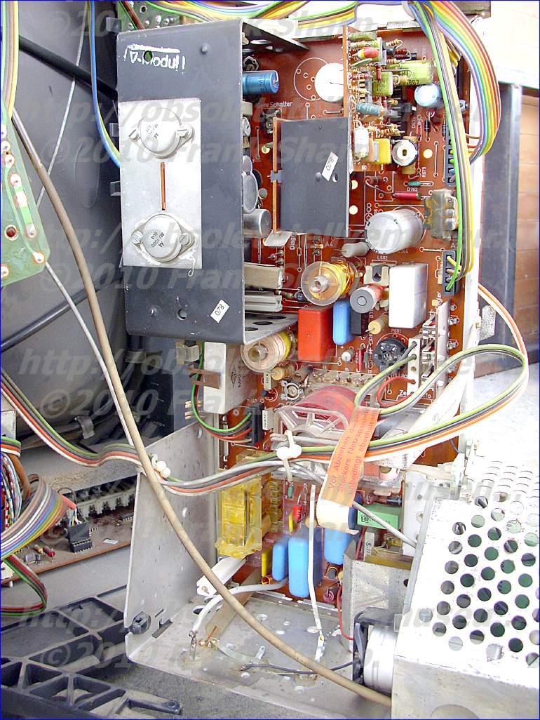
rgb amplifier video endstufen 7211506200 TBA 530 TBA990
CHROMA UNIT FARB BAUSTEIN 7211506000 TBA510 TBA540
LUMINANCE UNIT LUMINANZ FARB BAUSTEIN 7211506100 TBA970
SOUND AMPL UNIT TON ENDSTUFE 7211506300
LINE OSC + SYNCHRONIZATIONN COM ZEILEN OSC 7211521100 TBA920
E/W CORRECTION UNIT O/W KISSEN KORR 7325 321200
TBA920 line oscillator combination
 DESCRIPTION
The line oscillator combination TBA920 is a monolithic
integrated circuit intended for the horizontal deflection of the black and white
and colour TV sets
picture tube.
FEATURES:
SYNC-PULSE SEPARATION
OPTIONAL NOISE INVERSION
GENERATION OF A LINE FREQUENCY VOL-
TAGE BY MEANS OF AN OSCILLATOR
PHASE COMPARISON BETWEEN SYNC-
PULSE AND THE OSCILLATOR WAVEFORM
PHASE COMPARISON BETWEEN THE OS-
CILLATOR WAVEFORM AND THE MIDDLE OF
THE LINE FLY-BACK PULSE
AUTOMATIC SWITCHING OF THE VARIABLE
TRANSCONDUCTANCE AND THE VARIABLE
TIME CONSTANT TO ACHIEVE NOISE SUP-
PRESSION AND, BY SWITCHING OFF, POS-
SIBILITY OF TAPE-VIDEO-REGISTERED RE-
PRODUCTION
SHAPING AND AMPLIFICATION OF THE OS-
CILLATOR WAVEFORM TO OBTAIN PULSES
FOR THE CONTROL OF DRIVING STAGES IN
HORIZONTAL, DEFLECTION CIRCUITS
USING EITHER TRANSISTORS OR THYRISTORS,
THE Philips TBA SERIES
The TBA series of i.c.s developed by Philips for use in TV receivers comprises the TBA500Q, TBA510Q, TBA520Q, TBA530Q, TBA540Q, TBA550Q, TBA560Q, TBA750Q and TBA990Q, the Q signifying that the lead out pins are in zig-zag form as illustrated in other posts here at Obsolete Technology Tellye !
The operations the various i.c.s in this series perform are as follows:
TBA500Q: Luminance Combination. Luminance amplifier for colour receivers incorporating luminance delay line matching stages, gated black level clamp and a d.c. contrast control which maintains a constant black level over its range of operation. A c.r.t. beam limiter facility is incorporated, first reducing the picture contrast and then the brightness. Line and field flyback blanking can also be applied.
TBA510Q: Chrominance Combination. Chrominance amplifier for colour receivers incorporating a gain controlled stage, a d.c. control for saturation which can be ganged to the receiver's contrast control, burst gating and blanking, a colour killer, and burst output and PAL delay line driver stages.
TBA520Q: Chrominance Demodulator. Incorporates U and V synchronous demodulators, G-Y matrix and PAL V switch. This type will be superseded by
the TBA990Q (development of which was nearing completion in 1972) listed later.
TBA530Q: RGB Matrix. Luminance and colour difference signal matrix incorporating preamplifiers.
TBA540Q: Reference Combination. Decoder reference oscillator (with external crystal) and a.p.c. loop. Also provides a.c.c., colour killer and ident outputs. TBA550Q: Video signal processor for colour or monochrome receivers. This i.c. is the successor to the TAA700. It is very similar electrically to the TAA700. TBA560Q: Luminance and Chrominance Combination. Provides luminance and chrominance signal channels for a colour receiver. Although not equivalent to the TBA500Q and TBA510Q it performs similar functions to those i.c.s.
TBA750Q: Intercarrier Sound Channel. Incorporates five stage intercarrier sound limiter/amplifier plus quadrature detector and audio preamplifier. External
TBA990Q: Chrominance Demodulator. Incorporates U and V synchronous demodulators, G -Y matrix and PAL V switch. This is at the time in the final stages of development and was been available from March 1972 onwards. As I have given information previously on the TBA550Q and TBA750Q we may concentrate in this and the concluding post in the series on the colour receiver i.c.s. such as multistandard sets or bistandard color decoders here at Obsolete Technology Tellye !
Fig. 1 shows in block diagram form their application for luminance and chrominance signal processing. We will look first at the TBA520Q an
 d TBA530Q which are in use for example in the Philips G8 single standard colour chassis.
TBA530Q RGB Matrix Preamplifier:
The internal circuitry of this i.c. is shown in Fig. 2 while Fig. 3 shows the immediate external connections as used in the Philips G8 chassis. The chip layout is designed to ensure tight thermal coupling between all transistors to minimise thermal drift between channels and each channel has an identical layout to the others to ensure equal frequency response characteristics. The colour -difference signals are fed in at pins 2, 3 and 4 and the luminance input is at pin 5. Trl and Tr2 form the matrix in each channel, driving the differential amplifiers Tr3, Tr4, Tr5. The operating conditions are set by Tr5 and Tr7, using an external current -determining resistor connected to pin 7. Pin 6 is the chassis connection and pin 8 the 12V supply line connection (maximum voltage permitted 13.2V, approximate current consumption 30mA). External load resistors are connected to pins 1, 14 and 11 from a 200V line and the outputs are taken from pins 16, 13 and 10. The output pins are internally connected to the load resistor pins via Tr6
 which provides a zener-type junction giving a level shift appropriate
for driving the bases of the external output transistors directly.
External l0kpF capacitors are required between the output and load
resistor pins to bypass these zener junctions at h.f. Feedback from the
external output stages is fed in at pins 15, 12 and 9. A common supply
line should be used for this and any other i.c.s in the series used in
the decoder, to ensure that any changes in the black level caused by
variations in the supply voltage occur in a predictable way : the
stability of the supply should be not worse than ±3% due to operational
variations to limit changes in picture black level during receiver
operation. To reduce the possibility of patterning on the picture due to
radiation of the harmonics of the demodulation
which provides a zener-type junction giving a level shift appropriate
for driving the bases of the external output transistors directly.
External l0kpF capacitors are required between the output and load
resistor pins to bypass these zener junctions at h.f. Feedback from the
external output stages is fed in at pins 15, 12 and 9. A common supply
line should be used for this and any other i.c.s in the series used in
the decoder, to ensure that any changes in the black level caused by
variations in the supply voltage occur in a predictable way : the
stability of the supply should be not worse than ±3% due to operational
variations to limit changes in picture black level during receiver
operation. To reduce the possibility of patterning on the picture due to
radiation of the harmonics of the demodulation process the leads carrying the drive signals to the tube should be kept
as short as possible : resistors (typically 1.51J) connected in series
with the leads and mounted close to the collectors of the out- put
transistors provide useful additional filtering of these harmonics.
process the leads carrying the drive signals to the tube should be kept
as short as possible : resistors (typically 1.51J) connected in series
with the leads and mounted close to the collectors of the out- put
transistors provide useful additional filtering of these harmonics. TBA520Q Chrominance Demodulator:
 In addition to U and V balanced synchronous detectors this i.c. incorporates a PAL switch which inverts on alternate lines the V reference signal fed to the V synchronous detector. The PAL switch is controlled by an integrated flip-flop circuit which is driven by line frequency pulses and is under the control of an ident input to synchronise the V switching. Outputs from the U and V demodulators are matrixed within the i.c. to obtain the G-Y signal so that all three colour difference signals are available at pins 4, 5 and 7. The internal circuit of this i.c. is shown in Fig. 4 while Fig. 5 shows the immediate external circuitry as used in the Philips G8 chassis. The separated U and ±V chrominance signals from the PAL delay line/matrix circuit are fed in at pins 9 and 13 respectively. The U and V reference signals, in phase quadrature, are fed in at pins 8 and 2. Taking the U channel first we see that the U chrominance signal is fed to Tr18 base. This transistor with Tr19 forms a differential pair which drives the emitters of the transistors-Tr4, Try, Tr6 and Tr7-which comprise the U synchronous demodulator. The U reference signal is fed to Tr12 base, this transistor with Tr13 forming a further differential pair which drive the bases of the synchronous demodulator transistors. The B -Y signal is developed across R3 and appears at output pin 7. A similar arrangement is followed in the V channel except that here the V reference signal fed in at pin 2 to the base of Tr22 is routed to the V synchronous demodulator (Tr8-Tr11) via the PAL switch Tr14-Tr17. This switch is controlled by the integrated flip-flop (bistable) Tr24 and Tr25 (with diodes DI and D2). The bases of the transistors in the flip-flop circuit are driven by negative goin
 g
line frequency pulses fed in at pins 14 and 15. As a result half line
frequency antiphase squarewaves are developed across R13 and R14 and fed
to the PAL switch via R57 and R58. The ident signal is fed into the
base of Tr32 at pin 1. A positive -going input to pin 1 drives Tr32 on
so that the base of Tr24 is shorted and the flip-flop rendered inactive
until the positive input is removed. In the Philips circuit a 4V peak
-to -peak 7.8kHz sinewave ident signal is fed in at pin 1 to synchronise
the flip-flop. The squarewave signal is externally available at pin 3
from the emitter -follower Tr39 which requires an external load
resistor. The R-Y signal developed across R9 is fed via R10 to output
pin 4. The G-Y signal appears at the output of the matrix network R4, R5
and R6 and is fed via R7 to pin 5. The d.c. voltages applied to pins 11
and 12 establish the correct G -Y and R-Y signal levels relative to the
B -Y signal. Pin 10 is internally connected and no external connection
should be made to this pin. The U and V reference carrier inputs should
be about IV p -p, via a d.c. blocking capacitor in each feed. These
inputs must not be less than 0-5V. The flip-flop starts when the voltage
at pin 1 is reduced The amplitudes of the pulses fed in at pins 14 and
15 below 0.4V : it should not be allowed to exceed -5V. to drive the
flip-flop should be between 2.5 and 5V p-p.
g
line frequency pulses fed in at pins 14 and 15. As a result half line
frequency antiphase squarewaves are developed across R13 and R14 and fed
to the PAL switch via R57 and R58. The ident signal is fed into the
base of Tr32 at pin 1. A positive -going input to pin 1 drives Tr32 on
so that the base of Tr24 is shorted and the flip-flop rendered inactive
until the positive input is removed. In the Philips circuit a 4V peak
-to -peak 7.8kHz sinewave ident signal is fed in at pin 1 to synchronise
the flip-flop. The squarewave signal is externally available at pin 3
from the emitter -follower Tr39 which requires an external load
resistor. The R-Y signal developed across R9 is fed via R10 to output
pin 4. The G-Y signal appears at the output of the matrix network R4, R5
and R6 and is fed via R7 to pin 5. The d.c. voltages applied to pins 11
and 12 establish the correct G -Y and R-Y signal levels relative to the
B -Y signal. Pin 10 is internally connected and no external connection
should be made to this pin. The U and V reference carrier inputs should
be about IV p -p, via a d.c. blocking capacitor in each feed. These
inputs must not be less than 0-5V. The flip-flop starts when the voltage
at pin 1 is reduced The amplitudes of the pulses fed in at pins 14 and
15 below 0.4V : it should not be allowed to exceed -5V. to drive the
flip-flop should be between 2.5 and 5V p-p. For a colou bar signal a U input of approximately 360mV is required at pin 9 and a V input of approximately 500mV is required at pin 13. The supply is fed in at pin 6 and this also sets the d.c. level of the B-Y output signal. The maximum voltage allowed at this pin is 13.2V. In early versions of the Philips G8 chassis a TAA630 i.c. was used in place of the TBA520Q.
Philips TBA SERIES SINCE the last part in this series Philips have released details of a PAL -D decoder developed in their laboratories in which most of the circuitry has been integrated into four i.c.s a TBA560Q which undertakes the luminance and chrominance signal processing, a TBA540Q which provides the reference signal channel, a TBA990Q which provides synchronous demodulation of the colour -difference signals, G -Y signal matrixing and PAL V switching, and a TBA530Q which matrixes the colour -difference signals and the luminance signal to obtain the R, G and B signals which after amplification by single -transistor output stages drive the cathodes of the shadowmask tube.
The TBA540Q and TBA560Q and also the TBA500Q and TBA510Q which provide an alternative luminance and chrominance signal processing arrangement will be covered this time.
The internal circuits of the TBA530Q and TBA520Q (predecessor to the TBA990Q which shows how fast things are moving at present) were shown in Part 6 in order to give an idea of the type of circuitry used in these linear colour receiver i.c.s. The internal circuitry is not however of great importance to the user or service engineer: all we need to know about a particular i.c. are the functions it performs, the inputs and outputs it requires and provides and the external connections necessary. The i.c.s we shall deal with in this instalment are highly complex internally the TBA560Q for example contains some 67 integrated transistor elements alone. This time therefore we shall just show the immediate external circuitry in conjunction with a block diagram to indicate the functions performed within the i.c.
TBA540Q Reference Signal Channel:

A block diagram with external connections for this i.c. is shown in Fig. 1. In addition to providing the reference signal required for synchronous demodulation of the colour difference signals this i.c. incorporates automatic phase and amplitude control of the reference oscillator and a half line frequency synchronous demodulator which compares the phases and amplitudes of the burst ripple and the square waveform from the PAL V switch circuit in order to generate a.c.c., colour killer and ident outputs. The use of a synchronous demodulator for these functions provides a high standard of noise immunity in the decoder. The internal reference oscillator operates in conjunction with an external 4.43MHz crystal connected between pins 1 and 15. The nominal load capacitance of the crystal is 20pF. The reference oscillator output, in correct phase for feeding to the V signal synchronous demodulator, is taken from pin 4 at a nominal amplitude of 1.5V peak -to -peak. This is a low -impedance output and no d.c. load to earth is required here. The bifilar inductor Ll provides the antiphase signal necessary for push-pull reference signal drive to the burst detector circuit, the antiphase input being at pin 6. The U subcarrier is obtained from the junction of a 900 phase shift network (R1, C1) connected across Ll. The oscillator is controlled by the output at pin 2. This pin is fed internally with a sinewave derived from the reference signal and controlled in amplitude by the internal reactance control circuit. The phase of the feedback from pin 2 to the crystal via C2 is such that the value of C2 is effectively increased. Pin 2 is held internally at a very low impedance. Thus the tuning of the crystal is automatically controlled by the amplitude of the feedback waveform and its influence on the effective value of C2. The burst signal is fed in at pin 5. A burst waveform amplitude of 1V peak -to -peak is required (the minimum threshold is 0.7V) and this is a.c. coupled. The a.p.c. loop phase detector (burst detector) loads and filter (R2, C4, C5 and C6) are connected to pins 13 and 14. A synchronously -generated a.c.c. potential is produced at pin 9. The voltage at this pin is set by R3 to 4V with zero burst input. The synchronous demodu- lator producing this output is fed with the burst signal and the PAL half line frequency squarewave which is a.c. coupled at pin 8 at 2.5V peak -to -peak. If the phase of the squarewave is correct the potential at pin 9 will fall and normal a.c.c. action will commence. If the phase of the squarewave is incorrect the voltage at pin 9 will rise, providing the ident action as this rise will make the PAL switch miss a count thereby correcting its phase. A colour -killer output is provided at pin 7 from an internal switching transistor. If the ident conditions are incorrect this transistor is saturated and the output at pin 7 is about 250mV. When the ident conditions are correct (voltage at pin 9 below 2.5V) the transistor is cut off providing a positive -going turn -on bias at pin 7. The network between pins 10 and 12 provides filtering and a.c.c. level (R3) setting. The control connected to pin 11 is set so that in conjunction with the rest of the decoder circuitry the level of the burst signal at pin 5 under a.c.c. control is correct. The positive d.c. supply required is applied to pin 3 and the chassis connection is pin 16.
TBA560Q Chroma-Luminance IC:

A block diagram with external connections for this i.c. is shown in Fig. 2. The i.c. incorporates the circuits required to process the luminance and chrominance signals, providing a luminance output for the RGB matrix and a chrominance output for the PAL delay line circuit.
The luminance input is a.c. coupled from the luminance delay line terminating resistor at pin 3. This pin also requires a d.c. bias current which is obtained via the 22kI resistor shown. The brightness control is connected to pin 6: variation from OV to 1 2V at this pin gives a variation in the black level of the luminance output at pin 5 of from OV to 3V, which is a greater range than is needed in practice. The contrast control is connected to pin 2 and the potential applied here controls the gain of both the luminance and the chrominance channels so that the two signals track together correctly. Picture tube beam current limiting can be applied at either pin 6 or pin 2 (by taking the earthy side of one of the controls to a beam limiter network). To maintain correct picture black level it is preferable to apply the beam limiting facility to reduce the contrast. A positive going pulse timed to coincide with the back porch period is fed in at pin 10 to provide burst gating and to operate the black -level clamp in the luminance channel: the black -level clamp requires a charge storage capacitor which is connected to pin 4. The luminance output is obtained from an internal emitter follower at pin 5, an external load resistor of not less than 2kS2 being required here. The output has a nominal black level of 1.6V and 1V black -to -white amplitude. The chrominance signal is applied in push-pull to pins 1 and 15. A.c.c. is applied at pin 14, a negative going potential giving a 26dB control range starting at 1V and giving maximum gain reduction at 200mV. The saturation control is connected to pin 13 and the colour -killer potential is also applied to this pin : the chrominance channel is muted when the voltage at this pin falls below IV. The chrominance output, at an amplitude of about 2V peak -to -peak, is obtained at pin 9: an external network is required which provides d.c. negative feedback in the chrominance channel via pin 12. The burst output, at about 1V peak -to -peak, is obtained at pin 7. A network connected to this pin also provides d.c. feedback to the chrominance input transformer (connected between pins 1 and 15) to give good d.c. stability. Line and field blanking pulses are fed in at pin 8 to the luminance and chrominance channels : these negative -going pulses should not exceed -5V in amplitude. The d.c. supply is applied to pin 11 and pin 16 is the chassis connection.
TBA500Q Luminance IC:
A block diagram with external connections for this i.c. is shown in Fig. 3. This i.c. provides a colour receiver luminance channel incorporating luminance delay -line matching stages, a black -level clamp and a d.c. contrast control which maintains a constant black level over its range of operation. A beam current limiting facility which first reduces picture ,contrast and then picture brightness is provided and line and field flyback blanking can be applied. A video input signal of 2V peak -to -peak with negative -going sync pulses is required at pin 2, a.c. coupled. A clamp potential obtained from pin 13 via a smoothing circuit is fed to pin 2 to regulate the black level of the signal at pin 2 to about 10-4V. The smoothing network for the black -level control potential should have a time -constant which is less than the time constant of the video signal coupling network. The 3V peak -to -peak composite video output with positive -going sync pulses obtained at pin 3 from an emitter -follower can be used as a source of chroma signal: in Fig. 3 it is used as a source of sync pulses for the black -level clamp, fed in at pin 15. This pin requires positive -going sync pulses of 2V amplitude or greater for sync -cancelling the black -level clamp. The other input to the clamp consists of negative going back porch pulses fed in at pin 1 to operate th
 e
clamp. The timing of these pulses is not critical provided the pulse
does not encroach on the sync pulse period and that it dwells for at
least Zus on any part of the back porch-clamp pulse overlap into the
picture line period is unimportant. A low-pass filter capacitor for the
clamp is connected at pin 14 to prevent the operation of the clamp being
affected by the bursts or h.f. noise. The contrast control is connected
to pin 5 and is linked to the saturation control so that the two track
together. A variation of from 2 to 4V at pin 5 gives a control range of
at least 40dB, the relationship between the video at pin 4 and the
potential at pin 5 being linear. An output to drive the luminance delay
line is provided at pin 4. This is a low -impedance source and a
luminance delay line with a characteristic impedance of 1-2.7161 can be
used. The delayed luminance signal is fed back into the i.c. at pin 8.
Line and field flyback banking pulses and the brightness control are
also connected to this pin. The gain of the luminance channel is
determined by the value of the resistor connected to pin 9. The
luminance output is taken from an emitter -follower at pin 10, an
external load resistor being required. The voltage output range
available is from 0.7V to 5-5V. The potential of the black level of the
output signal is normally set to 1.5V by appropriate setting of the
potential at pin 8. A luminance signal output amplitude of 2.8V black to
white at maximum contrast is produced : superimposed on this is the
blanking waveform which remains of constant amplitude independently of
the contrast and brightness control settings. A beam current limiting
input is provided at pin 6. A rising positive potential at this pin will
start to reduce the contrast at about 2V. Further increase in the
voltage at this pin will continue to reduce the contrast until a
threshold is reached, determined by the potential applied to pin 7, when
the d.c. level of the video signal is reduced giving reduction in
picture brightness. The d.c. supply is connected to pin 12 and pin 16 is
the chassis connection.
e
clamp. The timing of these pulses is not critical provided the pulse
does not encroach on the sync pulse period and that it dwells for at
least Zus on any part of the back porch-clamp pulse overlap into the
picture line period is unimportant. A low-pass filter capacitor for the
clamp is connected at pin 14 to prevent the operation of the clamp being
affected by the bursts or h.f. noise. The contrast control is connected
to pin 5 and is linked to the saturation control so that the two track
together. A variation of from 2 to 4V at pin 5 gives a control range of
at least 40dB, the relationship between the video at pin 4 and the
potential at pin 5 being linear. An output to drive the luminance delay
line is provided at pin 4. This is a low -impedance source and a
luminance delay line with a characteristic impedance of 1-2.7161 can be
used. The delayed luminance signal is fed back into the i.c. at pin 8.
Line and field flyback banking pulses and the brightness control are
also connected to this pin. The gain of the luminance channel is
determined by the value of the resistor connected to pin 9. The
luminance output is taken from an emitter -follower at pin 10, an
external load resistor being required. The voltage output range
available is from 0.7V to 5-5V. The potential of the black level of the
output signal is normally set to 1.5V by appropriate setting of the
potential at pin 8. A luminance signal output amplitude of 2.8V black to
white at maximum contrast is produced : superimposed on this is the
blanking waveform which remains of constant amplitude independently of
the contrast and brightness control settings. A beam current limiting
input is provided at pin 6. A rising positive potential at this pin will
start to reduce the contrast at about 2V. Further increase in the
voltage at this pin will continue to reduce the contrast until a
threshold is reached, determined by the potential applied to pin 7, when
the d.c. level of the video signal is reduced giving reduction in
picture brightness. The d.c. supply is connected to pin 12 and pin 16 is
the chassis connection.TBA510Q Chrominance IC:

A block diagram with external connections for this i.c. is shown in Fig. 4. It provides a colour receiver chrominance signal processing channel with a variable gain a.c.c. chroma amplifier circuit, d.c. control of chroma saturation which can be ganged to the opera- tion of the contrast control, chroma blanking and burst gating, a burst output stage, colour -killer circuit and PAL delay line driver stage. The chroma signal is a.c. coupled to pin 4, the a.c.c. control potential being applied at pin 2. The non - signal side of the differential amplifier used for the a.c.c. system is taken to pin 3 where a decoupling capacitor should be connected. A resistor can be connected between pins 2 and 3 to reduce the control sensitivity of the a.c.c. system to any desired level. The saturation control is connected to pin 15, the d.c. control voltage range required here being 1.5-4-5V. For chrominance blanking a negative -going line flyback pulse of amplitude not greater than 5V is fed in at pin 14. A series network is connected to pin 6 to decouple the emitter of one of the amplifying stages in the i.c.: the value of the resistor in this network influences the gain of both the burst and the chroma channels in the i.c. The chrominance signal outputs are obtained at pin 8 (collector) to drive the chroma delay line and pin 9 (emitter) to feed the chrominance signal matrix (undelayed signal). A resistive path to earth is essen- tial at pin 9. The colour -killer turn -on bias is applied to pin 5 : colour is "on" at 2.3V, "off" at 1.9V. Chroma signal suppression when killed is greater than 50dB. The burst signal output is at pin 11 (collector) or 12 (emitter). If a low -impedance output is required pin 11 is connected direct to the 12V supply rail and the output is taken from pin 12. An external load of 2kn connected to chassis is required here. The burst gating pulse is fed in at pin 13, a negative -going pulse of not greater than 5V amplitude being required. Pins 7 and 10 are connected to an internal screen whose purpose is to prevent unwanted burst and chroma outputs : the pins must be linked together and taken via a direct path to earth. Pin 1 is the d.c.
supply pin and pin 16 the chassis connection.
A TBA510 as example is used in the Grundig 1500/3010 series and also the YR 1972 Grundig colour chassis (5010 / 5050 series) introduced in the70's. Grundig continue in these models to favour colour -difference tube drive. The 5010 series uses a TBA510 together with a TAA630 colour demodulator i.c. in the chrominance section and a TBA970 luminance i.c. which drives a single BF458 luminance output transistor operated from a 280V rail. As this series has been appearing more and more i.c.s have come to be used in television receivers, both monochrome and colour, and more and more i.c.s designed for television set use have been announced. Some of these have been mentioned in recent argumentations here in this Web Museum. There seems little doubt that a major increase in the use of integrated circuits in television receivers is about to occur in the future. Fully integrated i.f. and vision detector sections are already in use (PHILIPS K9-K11) and this is the likely area, together with the decoder in colour sets, in which integration will most rapidly spread. Elsewhere integrated line and field oscillators using circuits without inductors have been developed and a field output stage in integrated form is now feasible. Line output stages consisting of hybrid i.c. and thick film circuits (PHILIPS K12) have been built and there is a programme of work directed to the integration of the r.f. tuner, using digital frequency synthesisers to provide local oscillator action controlled by signals from a remote point.
We seem to have reached the position where the only part of the set which does not attract the i.c. manufacturers is the picture tube itself !
SABA ULTRACOLOR PRO 6773 TELECOMMANDER-L CHASSIS FF032 VIDEO Amplifier suitable for use as a color CRT TUBE / kinescope driver:
A color kinescope matrix amplifier has a first input coupled through a capacitor to a source of color difference signals. Another input is coupled to a source of luminance signals. The matrix amplifier includes a cascode output stage direct current coupled to a cathode of a kinescope. A portion of a direct voltage developed at the cascode output amplifier is coupled to one input of a comparator circuit. The other input of the comparator circuit is coupled to a temperature compensated direct voltage reference source. The comparator is rendered operative during horizontal retrace intervals to provide a current to either charge or discharge the input capacitor in accordance with the difference between the voltage at the output of the cascode output amplifier and the reference voltage to compensate for voltage variations at the output of the cascode amplifier due to power supply variations and the like. To compensate for droop caused by the discharge of the input capacitor during the scanning interval, one input of a differential amplifier is included between the input capacitor and the input of the cascode output stage. Negative signal feedback is provided from the output stage to the other input of the differential amplifier via a capacitor arranged to be charged during the horizontal retrace interval. The two capacitors discharge at substantially the same rates during the scanning interval. By virtue of the common mode operation of the differential amplifier droop effects are minimized.
1. In a tel
amplifying means for combining said chrominance signals and said luminance signals, said amplifying means including first and second input terminals and an output terminal, said output terminal being direct current coupled to said image reproducing device, said second input terminal being direct current coupled to said source of said luminance signals;
first capacitive means for coupling said chrominance signals to said first input terminal;
comparator means having first and second input terminals for comparing voltages applied thereto, said comparator means being normally inoperative;
a relatively low level stabilized reference voltage source coupled to said first input terminal of said comparator means;
means coupled to said second input terminal of said comparator means for providing a direct voltage proportional to the direct voltage developed at said output terminal;
means for selectively rendering said comparator operative in response to said horizontal blanking pulses; and
current converting means coupled to said comparator and to said first capacitive means for charging and discharging said capacitive means to a direct voltage level in relation to the difference in voltage between said first and second input terminals of said comparator means so as to counteract the changes of the voltage developed at said output terminal.
2. The apparatus recited in claim 1 wherein said amplifying means includes:
a differential amplifier having first and second input terminals and an output terminal, said first input terminal being coupled to sai
second capacitive means coupled to said second input terminal of said differential amplifier; and
means for selectively charging said second capacitive means during said horizontal retrace interval, said first and second capacitive means being selected to have substantially equal discharging rates during the time intervals between said horizontal retrace intervals.
3. The apparatus recited in claim 2 wherein said second capacitive means is coupled between said output terminal of said ampl
 ifying means and said second input terminal of said differential amplifier. 4. The apparatus recited in claim 3 wherein said amplifying means includes a cascode amplifier coupled between the output of said differential amplifier and said output terminal of said amplifying means. 5. The apparatus recited in claim 3 wherein said amplifying means includes first and second transistors, the emitter of said first transistor being direct current coupled to the collector of said second transistor, the base of said first transistor being coupled to said first input terminal of said amplifying means, the base of said second transistor being coupled to said second input terminal of said amplifying means, the emitter of said first transist
a differential amplifier having two input terminals and two output terminals, one of said input terminals being coupled to said reference voltage source, the other of said input terminals being coupled to said output terminal of said amplifier means; and
a current mirror circuit having an input and an output, one of said output terminals of said differential amplifier being coupled to said input terminal of said current mirror circuit, the other of said output terminals of said differential amplifier being coupled to the output of said current mirror circuit and to said first capacitor means.
10. The apparatus recited in claim 1 wherein said voltage reference source is temperature compensated. 11. In a television receiver including a color kinescope leaving a plurality of electron beam forming apparatus, a source of luminance signals, a source of a plurality of color difference signals, and a source of horizontal blanking pulses, said horizontal blanking pulses corresponding to the time interval during which said electron beams are horizontally retraced, the apparatus comprising:
a plurality of amplifiers, each of said amplifiers including
amplifying means for com
comparator means having first and second input terminals for comparing voltages applied thereto, said comparator means being normally inoperative,
means coupled to said second input terminal of said comparator means for providing a direct voltage proportional to the direct voltage developed at said output terminal,
means for selectively rendering said comparator operative in response to said horizontal blanking pulses, and
current converting means coupled to said comparator and to said capacitive means for charging and discharging said capacitive means to a direct voltage level in relation to the difference in voltage between said first and second input terminals of said comparator means so as to counteract the changes of the voltage developed at said output terminal; and a relatively low level stabilized reference
voltage source coupled to said first input terminals of each of said plurality of comparator means.
Description:
The present invention is directed to the field of amplifiers and is particularly directed to the field of amplifier arrangements utilized to drive color image reproducing devices such as kinescopes.
The electron guns of a color kinescope are typically driven by separate amplifier stages. Variations of the operating conditions of an amplifier stage, such as variations of the stage's supply voltage, tend to produce variations in the brightness of a reproduced image. Furthermore, because each of the stages tends to operate at different power dissipation levels the operating conditions of the stages vary with respect to each other and hence color imbalances may occur.
Athou
 gh supply voltage regulators and high level clamping circuits have been employed in conjunction with kinescope amplifier stages to inhibit the aformentioned problems, it is desirable to provide kinescope driver amplifier arrangements which maintain their operating point stability with variations in operating conditions such as power supply variations without the need of supply voltage regulators or high level clamping circuits.
Furthermore, it is desirable, because of the trend toward miniaturization in electronic art, that at least a portion of the kinescope amplifier driver should be able to be constructed in integrated circuit form.
It is also desirable to provide kinescope driver amplifier arrangements which include independent controls for adjusting the DC level and the AC amplitude of the signals coupled to the kinescope. This is particularly desirable where "precision-in-line" kinescopes or the like, in which the electron guns have common control electrodes, are employed since, in these types of kinescopes, it is difficult to independently adjust the operating conditions associated with the respective guns because of the commonality of control electrodes.
Furthermore, it is desirable that a kinescope driver amplifier which is to be utilized with a precision-in-line type of kinescope provide a relatively wide bandwidth without the requirement of high frequency peaking coils. Peaking coils tend to be bulky. In addition, undesirable voltages may be developed across a peaking coil due to the large magnetic fields which may be produced by the yokes associated with a precision-in-line kinescope. These undesirable voltages may produce disconcerting brightness and/or hue changes.
In accordance with the present invention, one input terminal of amplifying means is coupled to a source of chrominance signals through capacitive means. A second input of the amplifying means is direct current coupled to a source of luminance signals. The output terminal of the amplifying means is direct current coupled to a color image reproducing device such as a precision-in-line kinescope of the like. The amplifying means includes means for combining the luminance and chrominance signals to provide the image reproducing device with color signals. The amplifying means also includes comparator means for comparing the voltage developed at the output terminal to a reference voltage to generate a current to control the charging of the capacitive means in a manner so as to counter-act the changes of the voltage developed at the output due, for example, to changes in the power supply voltage. The comparator means is arranged to be normally inoperative and is selectively rendered operative during the horizontal retrace interval.
In accordance with another aspect of the present invention, the amplifying means includes a differential amplifier having first and second input terminals and an output terminal. The output terminal of the differential amplifier is coupled to the output terminal of the amplifying means. The first input terminal of the differential amplifier is coupled to the input terminal of the amplifying means. The second input terminal of the differential amplifying means is coupled to a second capacitive means. Means are provided for selectively charging the second capacitive means during the horizontal retrace interval. The first and second capacitive means are selected to have substantially equal discharging rates so as to compensate for any decrease in the DC content (i.e., droop) at the output terminal of the amplifying means during the scanning interval.
In accordance
 with still another feature of the present invention, the second capacitive means is coupled to the output terminal of the amplifying means in a manner so as to allow adjustment of the AC gain of the amplifying means. The DC conditions of the output of the amplifying means may be controlled by controlling the portion of the voltage developed at the output terminal coupled to the comparator means.
The present invention may best be understood by reference to the following detailed description and accompanying drawing which shows, partially in block diagram form and partially in schematic form, the general arrangement of a color television receiver employing a kinescope driver amplifier arrangement constructed in accordance with the present invention .
The color television receiver includes a video signal processing unit 141 responsive to radio frequency (RF) signals, received by an antenna, for receiving in a known manner, a composite video signal comprising chrominance, luminance, sound and synchronizing signal components.
The output of video processing unit 141 is coupled to a chrominance channel 142 including a chrominance processing unit 143 and a color demodulator 144. Chrominance processing unit 143 separates chrominance signals from the composite video signal. Color demodulator 144 derives signals of the appropriate polarity representing, for example, R-Y, G-Y and B-Y color difference signal informatio n from the chrominance signals. The TAA630 integrated circuit or similar circuit is suitable for use as color demodulator 144.
The output of video processing unit 141 is also coupled to a luminance channel 145 including a luminance processing unit 146 which amplifies and processes luminance components of the composite signal to form an output signal of the appropriate polarity representing luminance, Y, information. A brightness control unit 147 to control the DC content of luminance signal Y and a contrast control unit 148 to control the amplitude of luminance signal Y are coupled to processing unit 146.
The composite video signal is also coupled to a sync separator 149 which, in turn, is coupled to a horizontal deflection unit 151 and a vertical deflection unit 152. Horizontal deflection unit 151 is also coupled to a high voltage unit 154 which generates operating voltages for kinescope 153. Outputs from horizontal deflection unit 151 and vertical deflection unit 152 are coupled to luminance pr
 ocessing unit 146 to inhibit or blank luminance signal Y during the horizontal and vertical retrace intervals. Similarly, an output from horizontal deflection unit 151 may be coupled to chroma processing unit 143 or color demodulator 144 to inhibit the color difference signals during the horizontal retrace interval. Furthermore, first and second signals including positive going pulses, the pulses of each signal being coincident with the horizontal retrace or blanking interval, are coupled to matrix unit 100 to control its operation, as will appear below, via conductors 159 and 167, respectively.
The R-Y output signal and luminance signal Y are coupled to a matrix unit 100 where they are combined to form a color signal representing red (R) information. Similarly, the B-Y and G-Y color difference signals are respectively coupled to matrix-driver units 150 and 157, similar to the combination of matrix unit 100 and kinescope driver 199, where they are matrixed with luminance signal Y to produce color signals representing blue (B) and green (G) information. Since the matrix units for the various color difference signals are similar, only matrix unit 100 will be described in detail.
Matrix unit 100, enclosed within dotted line 160, is suitable for construction as an integrated circuit. The R-Y color difference signal is coupled through a capacitor 110 to the base of an NPN transistor 101 which is a
rranged as a common collector amplifier for color difference signals. Transistor 101, NPN transistor 102, resistors 178 and 184 form a summing circuit 161 for the color difference signal and luminance signal Y, the latter being direct current coupled to the base of transistor 102. The combined output of circuit 161, taken at the collector of transistor 102, is coupled to the base of an NPN transistor 105. Transistor 105 and an NPN transistor 106 form a differential amplifier 162 to which bias current is supplied from a current source including a suitably biased transistor 182. The output of differential amplifier 162, taken at the collector of transistor 105, is coupled through a level shifter, shown as the series connection of a zener diode 163, and a diode 165 to a kinescope 199. Bias current is provided for zener diode 163 and diode 165 through a resistor 183, which serves as the load resistor of transistor 105, and resistors 176 and 177.
Kinescope driver 199 comprises a cascode amplifier 164 including NPN transistors 120 and 119. The output of matrix unit 100 is coupled to the base of transistor 119 while a positive supply voltage (e.g. +12 volts) is coupled to the base of transistor 120. The output of kinescope driver 199, taken at the collector of transistor 120 is direct current coupled through a resistor 179 to the red (R) cathode of kinescope 153. The collector of transistor 120 is coupled to a source of supply voltage B+ through a load resistor 165. Supply voltage B+ is a relatively high voltage, typically, in the order of 200 to 300 vdc.
The collector of transistor 120 is also coupled to a series combination of a resistor 166 and a black level setting potentiometer 167, the latter being returned to ground. A direct voltage proportional to that at the collector of transistor 120 is developed at the wiper arm of potentiometer 167 and is coupled to one input of a voltage comparator circuit 168. Comparator 168 comprises NPN transistors 103 and 104 coupled as a differential amplifier. A second input of comparator 168, at the base of transistor 103, is coupled to a temperature compensated voltage reference (TCVR) unit 169. Voltage reference unit 169, which may, for example, be similar to that employed in the CA3085 integrated circuit manufactured by RCA Corporation, supplies a regulated reference voltage of approximately 1.6 vdc.
Voltage reference unit 169 is also coupled to the matrix portions of units 150 and 157 via conductor 155 so that a common reference voltage is coupled to the respective comparators of units 100, 150 and 157. It is noted that matrix unit 100 and the matrix portions of units 150 and 153 may be constructed as a single integrated circuit.
A current source including an NPN transistor 170 is coupled to the jointly connected emitters of transistors 103 and 104. The first horizontal blanking pulse signal generated by horizontal deflection unit 151 is coupled to the base of transistor 170 via conductor 159.
The output of differential amplifier 168 provided at the collector of NPN transistor 103 is converted to a bidirectional current by means of a current mirror circuit 180 comprising a diode-connected PNP transistor 172 and a PNP transistor 173. The collector of transistor 173 is coupled to the collector of transistor 104 and to the base of transistor 101.
The junction of resistors 166 and 167 is coupled to a signal feedback circuit comprising a series connection of a potentiometer 174 and a resistor 175. Feedback voltage developed at the wiper arm of potentiometer 174 is coupled through a capacitor 120 to the base of transistor 106 (i.e., one input of differential amplifier 162). The base of transistor 106 is returned to ground through resistor 181 and the collector-emitter junction of a transistor 108. The base of transistor 108 is coupled to horizontal deflection unit 151 to receive the first horizontal blanking pulse signal via conductor 159. An NPN transistor 107, the emitter of which is coupled to the base of transistor 106, is arranged together with resistor 181 and the collector-emitter junction of transistor 108 as an emitter follower. The base of transistor 107 is coupled to horizontal deflection unit 151 to receive the second horizontal blanking pulse signal via conductor 167. It is noted that this signal may also be generated within the IC device.
Kinescope 153 may be a precision-in-line kinescope such as the RCA type 15VADTCO1. As is described in U.S. Pat. No. 3,817,397, issued May 21, 1974, there is no provision for separate adjustment of red, green and blue gun screen and grid potentials and only the cathodes of the three guns of such a kinescope are available for separate adjustment of the cut off point of the guns. As will become apparent in the following description, matrix unit 100 and kinescope driver 199 are particularly suited to a kinescope of the precision-in-line type but it should be appreciated that they may be utilized for other types of kinescopes such as delta-gun, shadow mask or other slotted mask types.
In operation, the signal supplied to the base of transistor 107 during the scanning interval by horizontal deflection unit 151 is of sufficiently low amplitude (e.g., less than +4vdc) in relationship to the voltage at its emitter (controlled by the charge on capacitor 120 as will be explained) that it is non-conductive. Because of relatively low voltage applied to the bases of transistors 108 and 170 during the scanning interval, transistors 108, 170, 103 and 104 are also non-conductive and do not affect the operation of matrix circuit 100 during the scanning interval.
The signal -(R-Y), representing red color difference information, and the signal Y, representing luminance information, are coupled to amplifier 161 where they are combined in the emitter circuit of transistor 101 to form a signal -R, representing red information. The signal -R is further amplified and inverted twice by differential amplifier 162 and cascode amplifier 164 for application to kinescope 153.
It is noted that resistors 183, 176 and 177 should be selected so that zener diode 163 is biased well into its reverse breakdown region to inhibit noise.
The portion of the output signal of cascode amplifier 164 developed at the wiper arm of potentiometer 174, is capacitively fed back to one input of differential amplifier 162. This negative feedback arrangement, in conjunction with the use of cascode amplifier 199, provides for a relatively wide bandwidth, thereby eliminating the need for peaking coils or the like to improve high frequency response. The AC gain (or drive) of the matrix unit-kinescope driver arrangement may be adjusted by adjustment of the wiper arm of potentiometer 174 (normally a service or factory adjustment).
During the horizontal retrace interval, a relatively high voltage (e.g., approximately +6 vdc plus the base to emitter voltage of transistor 107 when transistor 107 is rendered conductive) is applied to the base of transistor 107 from horizontal deflection unit 151. Horizontal deflection unit 151 also applies a relatively high voltage to the bases of transistors 108 and 170. As a result transistors 107, 108, 170, 103 and 104 are rendered conductive and the base of transistor 106 is clamped to a voltage substantially equal to the voltage at the base of transistor 107 less the base emitter voltage of transistor 107 (e.g., +6 vdc). The voltage to which the base of transistor 106 is clamped is sufficiently lower than that at the base of transistor 105 so that transistor 106 will be rendered non-conductive and transistor 105 will be rendered fully conductive. Under these conditions, the voltage developed at the collector of transistor 120 will rise toward B+ to a voltage determined by t
he conduction of transistors 119 and 120 and the voltage division action of resistors 165, 166 and the impedance of potentiometer 167 in parallel combination with the series combination of potentiometer 174 and resistor 175.
While the base of transistor 106 is clamped to the voltage applied to the base of transistor 107 less the voltage developed between the base and emitter of transistor 107, the AC feedback provided by capacitor 120 is effectively disconnected and capacitor 120 is provided with a charging path including resistor 166 and a portion of potentiometer 174 by which it is rapidly charged to a voltage determined by the voltage at the emitter of transistor 107 and DC voltage developed at the collector of transistor 120.
The voltage developed at the wiper arm of potentiometer 167 is coupled to the base of transistor 104 and, during each horizontal retrace interval, is compared to the voltage developed at the base of transistor 103 by TCVR 169. A difference in voltage is converted by virtue of the current mirror configuration of transistors 172 and 173 into an error current at the junction of the collectors of transistors 104 and 173. The error current acts, depending on the relative levels at the bases of transistors 103 and 104, to charge or discharge capacitor 110.
Potentiometer 167 initially is adjusted to provide a voltage at the collector of transistor 120 sufficient to cut off the red gun of kinescope 153 when a black image signal is present. Therefore, it is desirable to select the values of resistors 165 and 166 and potentiometer 167 to ensure that the full range of black level control at the red cathode of kinescope 153 is available.
Matrix circuit 100 is arranged so that capacitor 110 will be charged or discharged in a manner to compensate for any change in B+. For example, if B+ decreases, the voltage developed at the base of transistor 104 will decrease relative to the stable reference voltage developed at the base of transistor 103. Therefore, the collector current of transistor 103 and the substantially equal currents flowing through the emitter-collector circuits of transistors 172 and 173 will increase, causing capacitor 110 to be charged. As a result, the voltage at the base of transistor 101 will increase, the voltage at the bas
e of transistor 105 will increase, the voltage at the collector of transistor 105 will decrease and the voltage at the collector of transistor 120 will increase.
It is noted that transistor 173 and transistor 104 operate in what may be termed a push-pull fashion in that the change in current flowing between the emitter and collector of transistor 173 is inversely related to the change in current flowing between the collector and the emitter of transistor 104. Thus, if the current flowing through the emitter-collector of transistor 104 increases, the current through the collector-emitter of transistor 173 decreases, so that capacitor 110 is discharged by the excess of current flowing through transistor 104 rather than being charged by current from transistor 173.
Thus, the feedback arrangement including TCVR 169 of matrix unit 100 adjusts the charge on capacitor 110 to compensate for, and therefore substantially eliminate, the effect on the direct voltage applied to the kinescope cathodes of variations in B+. Furthermore, it is noted that variations in other portions of the matrix amplifier driver arrangement (such as variations caused by temperature or component tolerance changes) affecting the DC conditions at the collector of transistor 120 will be compensated for by the arrangement in a similar manner.
The charge stored on capacitor 110 during the horizontal retrace interval serves to control the bias on cascode amplifier 164 during the succeeding scanning interval. It is noted that the charge on capacitor 110 is not affected by the color difference signals or luminance signals during the horizontal retrace interval, since these signals are arranged to be constant during the horizontal retrace interval.
After the horizontal retrace interval, transistors 103, 104, 170, 172, 173, 107 and 108 are rendered nonconductive (as previously described) and capacitors 110 and 120 begin to discharge. While capacitor 110 controls the bias voltage at the base of transistor 105, capacitor 120 controls the bias voltage at the base of transistor 106. Capacitors 110 and 120 and their associated discharging circuitry preferably are selected so that capacitors 110 and 120 discharge at substantially equal rates. The similar changes in voltage are applied to opposite sides of differential amplifier 162. The common mode rejection characteristics of differential amplifier 162 will prevent the discharging of capacitor 110 to be reflected in the DC conditions at the collector of transistor 120. This "droop" compensation feature provided by capacitor 120 in junction with differential amplifier 162 is desirable, since in its absence, capacitor 110 would have to be a relatively large value to prevent droop. This is especially undesirable if it is desired to construct matrix unit 100 as an integrated circuit because large currents, not compatible with integrated circuit technology, would be required to charge and discharge capacitor 110.
Typical values for the arrangement are shown on the accompanying drawing.
It should be noted that although the present invention has been described in terms of a particular configuration shown in the diagram, modifications may be made which are contemplated to be within the scope of the invention. For instance, cascode driver 199 may be placed with other driver stages well known in the art. Furthermore, the current mirror configuration comprising transistors 172 and 173 may be modified in accordance with other known current mirror configurations.
The electron guns of a color kinescope are typically driven by separate amplifier stages. Variations of the operating conditions of an amplifier stage, such as variations of the stage's supply voltage, tend to produce variations in the brightness of a reproduced image. Furthermore, because each of the stages tends to operate at different power dissipation levels the operating conditions of the stages vary with respect to each other and hence color imbalances may occur.
Athou
Furthermore, it is desirable, because of the trend toward miniaturization in electronic art, that at least a portion of the kinescope amplifier driver should be able to be constructed in integrated circuit form.
It is also desirable to provide kinescope driver amplifier arrangements which include independent controls for adjusting the DC level and the AC amplitude of the signals coupled to the kinescope. This is particularly desirable where "precision-in-line" kinescopes or the like, in which the electron guns have common control electrodes, are employed since, in these types of kinescopes, it is difficult to independently adjust the operating conditions associated with the respective guns because of the commonality of control electrodes.
Furthermore, it is desirable that a kinescope driver amplifier which is to be utilized with a precision-in-line type of kinescope provide a relatively wide bandwidth without the requirement of high frequency peaking coils. Peaking coils tend to be bulky. In addition, undesirable voltages may be developed across a peaking coil due to the large magnetic fields which may be produced by the yokes associated with a precision-in-line kinescope. These undesirable voltages may produce disconcerting brightness and/or hue changes.
In accordance with the present invention, one input terminal of amplifying means is coupled to a source of chrominance signals through capacitive means. A second input of the amplifying means is direct current coupled to a source of luminance signals. The output terminal of the amplifying means is direct current coupled to a color image reproducing device such as a precision-in-line kinescope of the like. The amplifying means includes means for combining the luminance and chrominance signals to provide the image reproducing device with color signals. The amplifying means also includes comparator means for comparing the voltage developed at the output terminal to a reference voltage to generate a current to control the charging of the capacitive means in a manner so as to counter-act the changes of the voltage developed at the output due, for example, to changes in the power supply voltage. The comparator means is arranged to be normally inoperative and is selectively rendered operative during the horizontal retrace interval.
In accordance with another aspect of the present invention, the amplifying means includes a differential amplifier having first and second input terminals and an output terminal. The output terminal of the differential amplifier is coupled to the output terminal of the amplifying means. The first input terminal of the differential amplifier is coupled to the input terminal of the amplifying means. The second input terminal of the differential amplifying means is coupled to a second capacitive means. Means are provided for selectively charging the second capacitive means during the horizontal retrace interval. The first and second capacitive means are selected to have substantially equal discharging rates so as to compensate for any decrease in the DC content (i.e., droop) at the output terminal of the amplifying means during the scanning interval.
In accordance
The present invention may best be understood by reference to the following detailed description and accompanying drawing which shows, partially in block diagram form and partially in schematic form, the general arrangement of a color television receiver employing a kinescope driver amplifier arrangement constructed in accordance with the present invention .
The color television receiver includes a video signal processing unit 141 responsive to radio frequency (RF) signals, received by an antenna, for receiving in a known manner, a composite video signal comprising chrominance, luminance, sound and synchronizing signal components.
The output of video processing unit 141 is coupled to a chrominance channel 142 including a chrominance processing unit 143 and a color demodulator 144. Chrominance processing unit 143 separates chrominance signals from the composite video signal. Color demodulator 144 derives signals of the appropriate polarity representing, for example, R-Y, G-Y and B-Y color difference signal informatio
n from the chrominance signals. The TAA630 integrated circuit or similar circuit is suitable for use as color demodulator 144. The output of video processing unit 141 is also coupled to a luminance channel 145 including a luminance processing unit 146 which amplifies and processes luminance components of the composite signal to form an output signal of the appropriate polarity representing luminance, Y, information. A brightness control unit 147 to control the DC content of luminance signal Y and a contrast control unit 148 to control the amplitude of luminance signal Y are coupled to processing unit 146.
The composite video signal is also coupled to a sync separator 149 which, in turn, is coupled to a horizontal deflection unit 151 and a vertical deflection unit 152. Horizontal deflection unit 151 is also coupled to a high voltage unit 154 which generates operating voltages for kinescope 153. Outputs from horizontal deflection unit 151 and vertical deflection unit 152 are coupled to luminance pr
The R-Y output signal and luminance signal Y are coupled to a matrix unit 100 where they are combined to form a color signal representing red (R) information. Similarly, the B-Y and G-Y color difference signals are respectively coupled to matrix-driver units 150 and 157, similar to the combination of matrix unit 100 and kinescope driver 199, where they are matrixed with luminance signal Y to produce color signals representing blue (B) and green (G) information. Since the matrix units for the various color difference signals are similar, only matrix unit 100 will be described in detail.
Matrix unit 100, enclosed within dotted line 160, is suitable for construction as an integrated circuit. The R-Y color difference signal is coupled through a capacitor 110 to the base of an NPN transistor 101 which is a
Kinescope driver 199 comprises a cascode amplifier 164 including NPN transistors 120 and 119. The output of matrix unit 100 is coupled to the base of transistor 119 while a positive supply voltage (e.g. +12 volts) is coupled to the base of transistor 120. The output of kinescope driver 199, taken at the collector of transistor 120 is direct current coupled through a resistor 179 to the red (R) cathode of kinescope 153. The collector of transistor 120 is coupled to a source of supply voltage B+ through a load resistor 165. Supply voltage B+ is a relatively high voltage, typically, in the order of 200 to 300 vdc.
The collector of transistor 120 is also coupled to a series combination of a resistor 166 and a black level setting potentiometer 167, the latter being returned to ground. A direct voltage proportional to that at the collector of transistor 120 is developed at the wiper arm of potentiometer 167 and is coupled to one input of a voltage comparator circuit 168. Comparator 168 comprises NPN transistors 103 and 104 coupled as a differential amplifier. A second input of comparator 168, at the base of transistor 103, is coupled to a temperature compensated voltage reference (TCVR) unit 169. Voltage reference unit 169, which may, for example, be similar to that employed in the CA3085 integrated circuit manufactured by RCA Corporation, supplies a regulated reference voltage of approximately 1.6 vdc.
Voltage reference unit 169 is also coupled to the matrix portions of units 150 and 157 via conductor 155 so that a common reference voltage is coupled to the respective comparators of units 100, 150 and 157. It is noted that matrix unit 100 and the matrix portions of units 150 and 153 may be constructed as a single integrated circuit.
A current source including an NPN transistor 170 is coupled to the jointly connected emitters of transistors 103 and 104. The first horizontal blanking pulse signal generated by horizontal deflection unit 151 is coupled to the base of transistor 170 via conductor 159.
The output of differential amplifier 168 provided at the collector of NPN transistor 103 is converted to a bidirectional current by means of a current mirror circuit 180 comprising a diode-connected PNP transistor 172 and a PNP transistor 173. The collector of transistor 173 is coupled to the collector of transistor 104 and to the base of transistor 101.
The junction of resistors 166 and 167 is coupled to a signal feedback circuit comprising a series connection of a potentiometer 174 and a resistor 175. Feedback voltage developed at the wiper arm of potentiometer 174 is coupled through a capacitor 120 to the base of transistor 106 (i.e., one input of differential amplifier 162). The base of transistor 106 is returned to ground through resistor 181 and the collector-emitter junction of a transistor 108. The base of transistor 108 is coupled to horizontal deflection unit 151 to receive the first horizontal blanking pulse signal via conductor 159. An NPN transistor 107, the emitter of which is coupled to the base of transistor 106, is arranged together with resistor 181 and the collector-emitter junction of transistor 108 as an emitter follower. The base of transistor 107 is coupled to horizontal deflection unit 151 to receive the second horizontal blanking pulse signal via conductor 167. It is noted that this signal may also be generated within the IC device.
Kinescope 153 may be a precision-in-line kinescope such as the RCA type 15VADTCO1. As is described in U.S. Pat. No. 3,817,397, issued May 21, 1974, there is no provision for separate adjustment of red, green and blue gun screen and grid potentials and only the cathodes of the three guns of such a kinescope are available for separate adjustment of the cut off point of the guns. As will become apparent in the following description, matrix unit 100 and kinescope driver 199 are particularly suited to a kinescope of the precision-in-line type but it should be appreciated that they may be utilized for other types of kinescopes such as delta-gun, shadow mask or other slotted mask types. In operation, the signal supplied to the base of transistor 107 during the scanning interval by horizontal deflection unit 151 is of sufficiently low amplitude (e.g., less than +4vdc) in relationship to the voltage at its emitter (controlled by the charge on capacitor 120 as will be explained) that it is non-conductive. Because of relatively low voltage applied to the bases of transistors 108 and 170 during the scanning interval, transistors 108, 170, 103 and 104 are also non-conductive and do not affect the operation of matrix circuit 100 during the scanning interval.
The signal -(R-Y), representing red color difference information, and the signal Y, representing luminance information, are coupled to amplifier 161 where they are combined in the emitter circuit of transistor 101 to form a signal -R, representing red information. The signal -R is further amplified and inverted twice by differential amplifier 162 and cascode amplifier 164 for application to kinescope 153.
It is noted that resistors 183, 176 and 177 should be selected so that zener diode 163 is biased well into its reverse breakdown region to inhibit noise.
The portion of the output signal of cascode amplifier 164 developed at the wiper arm of potentiometer 174, is capacitively fed back to one input of differential amplifier 162. This negative feedback arrangement, in conjunction with the use of cascode amplifier 199, provides for a relatively wide bandwidth, thereby eliminating the need for peaking coils or the like to improve high frequency response. The AC gain (or drive) of the matrix unit-kinescope driver arrangement may be adjusted by adjustment of the wiper arm of potentiometer 174 (normally a service or factory adjustment).
During the horizontal retrace interval, a relatively high voltage (e.g., approximately +6 vdc plus the base to emitter voltage of transistor 107 when transistor 107 is rendered conductive) is applied to the base of transistor 107 from horizontal deflection unit 151. Horizontal deflection unit 151 also applies a relatively high voltage to the bases of transistors 108 and 170. As a result transistors 107, 108, 170, 103 and 104 are rendered conductive and the base of transistor 106 is clamped to a voltage substantially equal to the voltage at the base of transistor 107 less the base emitter voltage of transistor 107 (e.g., +6 vdc). The voltage to which the base of transistor 106 is clamped is sufficiently lower than that at the base of transistor 105 so that transistor 106 will be rendered non-conductive and transistor 105 will be rendered fully conductive. Under these conditions, the voltage developed at the collector of transistor 120 will rise toward B+ to a voltage determined by t
While the base of transistor 106 is clamped to the voltage applied to the base of transistor 107 less the voltage developed between the base and emitter of transistor 107, the AC feedback provided by capacitor 120 is effectively disconnected and capacitor 120 is provided with a charging path including resistor 166 and a portion of potentiometer 174 by which it is rapidly charged to a voltage determined by the voltage at the emitter of transistor 107 and DC voltage developed at the collector of transistor 120.
The voltage developed at the wiper arm of potentiometer 167 is coupled to the base of transistor 104 and, during each horizontal retrace interval, is compared to the voltage developed at the base of transistor 103 by TCVR 169. A difference in voltage is converted by virtue of the current mirror configuration of transistors 172 and 173 into an error current at the junction of the collectors of transistors 104 and 173. The error current acts, depending on the relative levels at the bases of transistors 103 and 104, to charge or discharge capacitor 110.
Potentiometer 167 initially is adjusted to provide a voltage at the collector of transistor 120 sufficient to cut off the red gun of kinescope 153 when a black image signal is present. Therefore, it is desirable to select the values of resistors 165 and 166 and potentiometer 167 to ensure that the full range of black level control at the red cathode of kinescope 153 is available.
Matrix circuit 100 is arranged so that capacitor 110 will be charged or discharged in a manner to compensate for any change in B+. For example, if B+ decreases, the voltage developed at the base of transistor 104 will decrease relative to the stable reference voltage developed at the base of transistor 103. Therefore, the collector current of transistor 103 and the substantially equal currents flowing through the emitter-collector circuits of transistors 172 and 173 will increase, causing capacitor 110 to be charged. As a result, the voltage at the base of transistor 101 will increase, the voltage at the bas
It is noted that transistor 173 and transistor 104 operate in what may be termed a push-pull fashion in that the change in current flowing between the emitter and collector of transistor 173 is inversely related to the change in current flowing between the collector and the emitter of transistor 104. Thus, if the current flowing through the emitter-collector of transistor 104 increases, the current through the collector-emitter of transistor 173 decreases, so that capacitor 110 is discharged by the excess of current flowing through transistor 104 rather than being charged by current from transistor 173.
Thus, the feedback arrangement including TCVR 169 of matrix unit 100 adjusts the charge on capacitor 110 to compensate for, and therefore substantially eliminate, the effect on the direct voltage applied to the kinescope cathodes of variations in B+. Furthermore, it is noted that variations in other portions of the matrix amplifier driver arrangement (such as variations caused by temperature or component tolerance changes) affecting the DC conditions at the collector of transistor 120 will be compensated for by the arrangement in a similar manner.
The charge stored on capacitor 110 during the horizontal retrace interval serves to control the bias on cascode amplifier 164 during the succeeding scanning interval. It is noted that the charge on capacitor 110 is not affected by the color difference signals or luminance signals during the horizontal retrace interval, since these signals are arranged to be constant during the horizontal retrace interval.
After the horizontal retrace interval, transistors 103, 104, 170, 172, 173, 107 and 108 are rendered nonconductive (as previously described) and capacitors 110 and 120 begin to discharge. While capacitor 110 controls the bias voltage at the base of transistor 105, capacitor 120 controls the bias voltage at the base of transistor 106. Capacitors 110 and 120 and their associated discharging circuitry preferably are selected so that capacitors 110 and 120 discharge at substantially equal rates. The similar changes in voltage are applied to opposite sides of differential amplifier 162. The common mode rejection characteristics of differential amplifier 162 will prevent the discharging of capacitor 110 to be reflected in the DC conditions at the collector of transistor 120. This "droop" compensation feature provided by capacitor 120 in junction with differential amplifier 162 is desirable, since in its absence, capacitor 110 would have to be a relatively large value to prevent droop. This is especially undesirable if it is desired to construct matrix unit 100 as an integrated circuit because large currents, not compatible with integrated circuit technology, would be required to charge and discharge capacitor 110.
Typical values for the arrangement are shown on the accompanying drawing.
It should be noted that although the present invention has been described in terms of a particular configuration shown in the diagram, modifications may be made which are contemplated to be within the scope of the invention. For instance, cascode driver 199 may be placed with other driver stages well known in the art. Furthermore, the current mirror configuration comprising transistors 172 and 173 may be modified in accordance with other known current mirror configurations.
ULTRASONIC REMOTE CONTROL RECEIVER SABA ULTRACOLOR PRO 6773 TELECOMMANDER-L CHASSIS FF032 :An ultrasonic remote control receiver wherein an incoming ultrasonic signal is converted to square wave pulses of the same frequency by a Schmitt trigger circuit; digital circuits are thereafter used to count pulses resulting from the incoming signal over a predetermined period of time; a decoder activates one of a plurality of outputs in dependance to the number of pulses counted, provision is made to prevent interference signals from producing undesired control
outputs.

2. An ultrasonic remote control receiver comprising:
3. An ultrasonic remote control receiver comprising:
4. The ultrasonic remote control receiver as defined in claim 3, wherein said means producing square pulses is a Schmitt trigger circuit and said means providing a signal input to said sequence controller is a retriggerable monostable multivibrator.
5. An ultrasonic remote control receiver comprising:
6. An ultrasonic remote control receiver comprising:
7. An ultrasonic remote control receiver as defined in claim 6 further comprising a monostable multivibrator between the output of said Schmitt trigger circuit and the remaining elements of said receiver.
8. An ultrasonic remote control receiver as defined in claim 6 further comprising a bistable multivibrator between the output of said Schmitt trigger circuit and the remaing elements of said receiver.
9. The ultrasonic remote control receiver as defined in claim 7 wherein the hold period of said monostable multivibrator is slightly less than one half the period of said square wave pulses from said Schmitt trigger circuit.
Description:
The invention relates to an ultrasonic remote control receiver for receiving signals having different useful frequencies each associated with a channel, comprising a plurality of outputs which are each associated with one of the channels and from which a control signal is emitted on receipt of a signal having the corresponding useful frequency.To obtain the simplest possible transmitter construction in ultrasonic remote control, modulation of the emitted ultrasonic frequencies is not employed; to control different operations different frequencies are emitted which must be recognized in the receiver and evaluated for carrying out the different functions associated therewith. Presently, to recognize the different frequencies, use is made of resonant circuits, each of which contains one or more coils tuned in each case together
with a capacitor to one of the useful frequencies.
A further disadvantage is that the known receivers cannot be made by integrated techniques because the coils used therein are not suitable for such techniques.
The problem underlying the invention is thus to provide an ultrasonic remote control receiver of the type mentioned at above which is extremely simple to set and in addition can be made by integrated techniques.
To solve this problem, according to the invention an ultrasonic remote control receiver of the type mentioned above contains a counter for counting the useful frequency oscillations received during a fixed measuring time, a sequence control device which determines the measuring time and which is started on receipt of a useful frequency, and a decoder comprising several outputs which is connected to the outputs of the counter, said decoder emitting a control signal at the output associated with the count reached at the end of the measuring time.
In the receiver constructed according to the invention the frequency emitted by the transmitter is identified by counting the oscillations received during a measuring time. The evaluation of the count reached at the end of the measuring time takes place in a decoder which emits a control signal at a certain output according to the count. The measuring time is fixed by a sequence control device which is set in operation on receipt of useful frequency signals.
In such a receiver the only quantity which has to be exactly fixed is the measuring time; it is therefore no longer necessary to align components to certain frequencies. Since no coils are required, the novel receiver can also be made up of integrated circuits.
A further development of the invention resides in that an interference identifying device is provided which on receipt of interference frequencies differing from the useful frequencies interrupts the operation of the sequence control device.
Hitherto known ultrasonic remote control receivers respond to any oscillation received if the frequency thereof has a value which excites a resonant circuit in the receiver. There is no way of distinguishing between oscillations received from the remote control transmitter and from interference sources.
Interfering ultrasonic oscillations may be due to many different causes. For example, noises such as hand clapping, rattling of short keys such as safety keys, operating cigarette lighters, rattling of crockery and the like cover a frequency spectrum reaching from the audio frequency range far into the ultrasonic region. The ultrasonic components may have the effect of simulating a useful frequency and cause an erroneous function in the receiver.
The interference identifying device according to the further development is constructed in such a manner that it recognizes oscillations having frequencies deviating from the useful frequencies and as a result of this recognition switches off the sequence control device. This switching off prevents the counter state reached from being passed to the decoder and consequently the latter cannot emit an erroneous control signal.
With this further development of the ultrasonic remote control receiver the operation of equipment such as radio and television sets is made extremely reliable and interference-free. During the operation of such a set it is no longer possible for the remote control to become operative, triggered by interference noises, eliminating for example the possibility of unintentional program or volume changes.
Examples of embodiment of the invention are illustrated in the drawings, wherein:
FIG. 1 shows a block circuit diagram of a remote control receiver according to the invention;
FIG. 2 is a diagram explaining the mode of operation of the circuit according to FIG. 1;
FIG. 3 shows another embodiment of the invention;
FIG. 4 is a diagram explaining the mode of operation of the circuit according to FIG. 3;
FIG. 5 is a diagram illustrating interference frequency identification in the circuit according to FIG. 3;
FIG. 6 shows a block circuit diagram of another embodiment of part of the circuit according to FIG. 3;
FIG. 7 is a diagram explaining the mode of operation of the embodiment according to FIG. 6;
FIG. 8 is a block circuit diagram of a further embodiment of a part of the circuit according to FIG. and, an
FIG. 9 is a diagram explaining the mode of operation of the embodiment according to FIG. 8.
 The ultrasonic remote control receiver shown in FIG. 1 comprises an input 1 which is connected to an ultrasonic microphone intended to receive ultrasonic signals coming from a remote control transmitter. For each function to be performed by the receiver the remote control transmitter emits one of several unmodulated different useful frequencies which are spaced from each other a constant channel spacing Δ f and which all lie within a useful frequency band.
To obtain a signal which is as free as possible from noise at the input 1, a band filter and a limiting amplifier are preferably incorporated between the ultrasonic microphone and the input 1. The band filter may be made up of two active filters whose resonant frequencies are offset with respect to each other so that a pass band curve in the useful frequency band is obtained which is as flat as possible.
The output 3 of the Schmitt trigger 2 is also connected to the input 4 of a monoflop 5 which is brought into its operating state by each pulse at the output 3 of the Schmitt trigger. It returns from this operating state to its quiescent state after expiration of a hold time depending on its intrinsic time constant if it does not receive a new pulse prior to expiration of this hold time. It is held in the operating state by each pulse received during the hold time until it finally flops back into the quiescent state when the interval between two successive pulses is greater than its hold time.
The output 15 of the monoflop circuit 5 is connected to the input 16 of a sequence control device 17 which is set in operation by the signal emitted in the operating state of the monoflop 5. Supplied
The mode of operation of the circuit of FIG. 1 will now be explained with the aid of the diagram of FIG. 2
 which shows the variation with time of the signals at the output 3 of the Schmitt trigger 2 and at the inputs 16 and 19 as well as the outputs 21, 22 and 23 of the sequence control device 17.
It will be assumed that a useful frequency oscillation is being received at the input 1. The Schmitt trigger 2 then emits at the output 3 rectangular pulses whose recurrence frequency is equal to the frequency of said useful frequency oscillation. The first pulse emitted by the Schmitt trigger 2 puts the monoflop 5 into its operating state. The hold time of the monoflop 5 is so dimensioned that for all useful frequencies occurring it is longer than the recurrence period of the rectangular pulses emitted at the output 3. The monoflop 5 therefore remains in its operating state for as long as the useful frequency oscillation is applied to the input 1 and supplies to the control input 16 of the sequence control device 17 a control signal throughout this time.
Due to the control signal applied to the input 16 the sequence control device 17 emits at its outputs 21, 22 and 23 in time with the pulses supplied to it via the Schmitt trigger 18 at the input 19 mutually offset control pulse sequences, the duration of the control pulses being equal to the time interval of the leading edges of the pulses supplied at the input 19 and thus equal to the period of the oscillation applied to the input 20 and the pulse sequences being offset with respect to each other by one pulse duration. The control pulses emitted by the sequence control device 17 perform the following functions:
b. Via the input 13 the second pulse occurring at the output 22 causes the store 12 to take on and to store the count of the counter 11 reached at the end of the first control pulse.
c. The third control pulse appearing at the output 23 resets the counter 11 via the reset input 24.
COntrol pulse sequences continue to be emitted for as long as the monoflop 5 remains in its operating state.
Since the stage outputs of the store 12 are permanently connected to the inputs of the decoder 14, the store content is continuously being decoded. The decoder 14 therefore emits a control signal at the output which is associated with the count contained in the store.
During each group of three offset control pulses of the three control pulse sequences emitted by the sequence control device 17, the counter 11 receives counting pulses from the frequency divider 8 only for the duration of the control pulse of the first control pulse sequence emitted at the output 21. The duration of this control pulse thus determines the measuring time during which the oscillations of the useful frequency signal received are counted. Since the duration of the control pulses emitted by the sequence control device 17 is however equal to the period of the oscillation applied to the input 20, the measuring time is fixed by the period of said oscillation.
The purpose of the monoflop 5 is to prevent interference frequencies supplied to the input 1 from producing at one of the outputs D0 to D9 of the decoder 14 a control signal which could lead to an erroneous function of the equipment being controlled. The interference sources usually encountered emit a frequency spectrum whose components lie predominantly in the audio region, i.e., below the ultrasonic region. If the hold time of the monoflop 5 is set to a value slightly greater than the period of the smallest useful frequency but smaller than the period of the highest interference frequency occurring, the monoflop 5 returns to its quiescent state before the end of the period of an interference frequency. Since in this state no signal is supplied to the control input 16 of the sequence control device 17, the latter is put out of operation and consequently the received signal cannot be evaluated because the count of the counter 11 is not transferred to the store 12 and thus no decoding takes place.
To facilitate understanding of the invention, the function of the circuit of FIG. 1 will now be explained numerically by way of example. The channel spacing Δ f will be taken as 1,200 c/s so that for a frequency of 100 c/s of the oscillation applied to the input 20 and thus a measuring time of 10 ms a division ratio of the frequency divider 7 of k = t . Δf = 12 results. It will further be assumed that ten different channel frequencies are to be evaluated; the counter 11 is therefore so connected that it has a capacity of 10. With these values, during the measuring time the counter 11 runs through several count cycles. This means that for the received frequency during the measuring time the counter 11 reaches its maximum count several times and then starts counting again from the beginning. The count reached at the end of the measuring time is however still a clear indication of the received useful frequency provided the number of useful frequencies having a channel spacing Δf is at the most equal to the counter capacity Z. The relationship between the useful frequency f received and the count reached at the end of each measuring time t while this useful frequency is being received is expressed by the following equation:
f = (k/t) . (n . Z + m + 0.5)
wherein
f = useful frequency received in c/s
t = measuring time in seconds
k = division ratio of the frequency divider 7
Z = capacity of the counter 11
n = number of count cycles passed through (integral)
m = count
The term 0.5 in brackets is a correction factor which ensures that a new count is reached whenever the received frequency differs at least by half the channel spacing Δf from the channel center frequency of the neighboring channel. With a channel spacing Δ of 1,200 c/s, a measuring time t of 10 ms, a division ratio k of the frequency divider 7 of 12, a capacity Z of the counter 11 of 10 and an input frequency f of 33 k c/s, the count 7 is for example reached after two complete count cycles. This is because the input frequency of 33 k c/s is first divided by 12 by the frequency divider 7 so that pulses having a recurrence frequency of 2.750 k c/s reach the input 10 of the counter 11. Since the frequency divider 7 emits counting pulses only during the measuring time of 10 ms, during said time only 27.5 pulses reach the input 10 of the counter 11. For this number of pulses the counter thus runs through two complete cycles and finally stops at the count 7. Similarly, for an input frequency of 39 k c/s the counter stops at the count 2 after passing through three complete counter cycles. With the numerical values given up to 10 different frequencies may be received without any ambiguity occurring in the evaluation.
FIG. 3 illustrates a further embodiment of an ultrasonic remote control receiver which differs from the embodiment described above primarily in that to fix the measuring time it is not necessary to supply a reference frequency.
 In the illustration of FIG. 3 the same reference numerals as in FIG. 1 are used for identical circuit components. The part of the circuit enclosed in the dashed line represents the sequence control device 17' which emits at its outputs 21', 22', 23' control signals which have substantially the same functions as the control signals emitted at the outputs 21, 22 and 23 of the sequence control device 17 of FIG. 1.
The useful frequency signal received is again supplied to the input 1. The input 1 is connected to the input of the Schmitt trigger 2 which again converts the input useful frequency oscillations into a sequence of pulses whose recurrence frequency is equal to the input useful frequency. The output 3 of the Schmitt trigger 2 is connected to the input B1 of a monoflop 25 which is contained in the sequence control device 17' and which is so constructed that it is switched to its operating state by a pulse received at the input B1 but during its hold time cannot be tripped again by any further pulse. The output 3 of the Schmitt trigger 2 is also connected to the input 26 of an AND gate 27 whose other input 28 is connected to that output 21' of the sequence control device 17' which is directly connected to the output Q1 of the monoflop 25. The output Q1 of the monoflop 25 which emits the signal complementary to the signal at the output Q1 is connected to the input B2 of a further monoflop 29 whose output Q2 is connected to the input A1 of the monoflop 25. The input 10 of the counter 11 is connected to the output of the AND gate 27. The stage outputs of the counter 11 are connected to the inputs of a gate circuit 30 which on receipt of a control pulse at its input 31 transfers the count contained in the counter 11 to the decoder 14 connected to its outputs. In the decoder 14 the count is then decoded in the manner already explained in conjunction with FIG. 1 so that a control signal is emitted at the output corresponding to the transferred count.
The output of the AND gate 33 represents the output 22' of the sequence control circuit 17' which is directly connected to the control input 31 of the gate circuit 30. In addition, the output of the AND gate 33 is directly connected to one input 40 of a NOR gate 41 and to the other input 42 thereof via a delay member 43 and an inverter 44. The output of the NOR gate 41 represents the output 23' of the sequence control circuit 17', to which output the reset input 24 of the counter 11 is connected.
The mode of operation of the circuit of FIG. 3 is explained in FIG. 4. Since the measuring time in the arrangement of FIG. 3 is substantially shorter than in the arrangement of FIG. 1, the time scale in FIG. 4
 has been enlarged compared with FIG. 2 in order to clarify the illustration. When useful frequency oscillations are supplied to the input 1 of the receiver, pulses whose recurrence frequency is equal to the useful frequency appear at the output 3 of the Schmitt trigger 2. It will be assumed that the presence of a pulse corresponds to the logical signal value 1 whereas a pulse space represents the logical signal value 0. The leading edge of the first pulse at the output 3 puts the monoflop 25 into its operating state in which it emits the signal value 1 for the duration of its hold time at its output Q1, resulting in the control pulse at the output 21', which passes to the input 28 of the AND gate 27. Since the other input 26 of the AND gate 27 is directly connected to the output 3 of the Schmitt trigger 2, for the duration of each pulse at the output 3 the signal value 1 is also applied to the input 26 of the AND gate 27. Thus, the pulses occurring at the output 3 of the Schmitt trigger 2 are transferred for the duration of the control pulse at the output 21', i.e. during the hold time of the monoflop 25, as count pulses to the counter 11 and counted by the latter. The hold time of the monoflop 25 thus determines the measuring time; the capacity of the counter 11 must be greater than the number of pulses received during the measuring time for the greatest useful frequency. The count of the counter 11 reached at the end of the measuring time is then a clear indication of the received useful frequency.
When the monoflop 25 flops back into the quiescent state at the end of its hold time, it applies the signal value 0 via its output Q1 to the input 28 of the AND gate 27 so that no further count pulses can enter the counter 11. At the same time there appears at the output Q1 of the monoflop 25 the signal value 1 which at the input B2 puts the monoflop 29 into the operating state. In this state the monoflop 29 emits at its output Q2 the signal value 1 which blocks the monoflop 25 via the input A1 for the duration of the hold time of the monoflop 29 in such a manner that it cannot be switched into the operating state by pulses at the input B1. This is necessary to enable the sequence control device 17' to have sufficient time to generate the control pulses appearing at the outputs 22' and 23' for the transfer of the count or resetting of the counter.
With the return of the monoflop 25 to its quiescent state, the signal value 0 passes to the input 26 of the NOR gate 35 directly connected to the output Q1. During the operating state of the monoflop 25 the signal value 0 is applied with a delay determined by the delay member 38 via the inverter 39 to the input 37 of the NOR gate 35, said signal value 0 being replaced by the signal value 1 only after the delay time of the delay member 38 and not simultaneously with the flop back of the monoflop 25. Thus, for the duration of this delay time the signal value 0 is applied to both inputs 36 and 37 of the NOR gate 35 and consequently for this period of time the signal value 1 appears at the output of the NOR gate 35. The circuits 35, 38, 39 thus effect the generation of a short pulse which immediately follows the return of the monoflop 25 and the duration of which is determined by the delay of the delay member 38. This pulse is applied to the input 34 of the AND gate 33 (FIG. 4). The same effect could obviously alternatively be obtained with a monoflop which is tripped by the signal at the output Q1 changing from the value 1 to the value 0.
Now, if during this time a pulse is emitted at the output 3 of the Schmitt trigger 2, i.e., a signal value 1 is at the input 32 of the AND gate 33, said gate supplies to the control input 31 of the gate circuit 30 a control pulse for the duration of the delay of the delay member 38. This control pulse opens the gate circuit so that it allows the count reached at the end of the hold time of the monoflop 25 to pass to the decoder 14. The latter then emits a control signal at the output associated with this count. The signal value 1 present at the output of the AND gate 33 during the delay of the delay member 38 also passes directly to the input 40 of the NOR gate 41, at the other input 42 of which the signal value 0 is applied for the duration of the same pulse but with a delay determined by the delay member 43. Thus, in a manner similar to the circuits 35, 38, 39 the circuits 41, 43, 44 produce a short pulse which immediately follows the end of the output pulse of the AND gate 33 and appears at the output 23' of the sequence control circuit and is applied to the reset input 24 of the counter 11 (FIG. 4). This pulse resets the counter 11.
The hold time of the monoflop 29 is so set that it flops back into its quiescent state again only when the transfer process from the counter to the decoder via the gate circuit and the resetting of the counter has been effected. When the monoflop 29 returns to its quiescent state, it emits at its output Q2 the signal value 0 which brings the monoflop 25 via the input A1 thereof into such a condition that it can again be brought into its operating state by a pulse at the output 3 of the Schmitt trigger 2. In this manner the measuring and evaluating periods can be repeated for as long as useful frequency oscillations are supplied to the input 1.
In the circuit according to FIG. 3, interference frequencies are suppressed by setting a certain hold time of the monoflop 25. It is apparent from the above description of the function that the transfer of the count of the counter 11 to the decoder 14 takes place immediately following the end of the hold time of the monoflop 25, i.e., immediately following the end of the measuring time. However, a control signal initiating the transfer can be applied by the AND gate 33 to the control input 31 of the gate circuit 30 only when simultaneously with the end of the measuring time a pulse, i.e., the signal value 1, is present at the output 3 of the Schmitt trigger 2. Now, if the hold time of the monoflop 25 is made equal to the reciprocal of the channel spacing Δf, this coincidence at the AND gate 33 at the end of the measuring time occurs only when quite definite frequencies are applied to the input 1; these frequencies lie only within frequency bands which in the example described here, in which the output pulses of the Schmitt trigger 2 have a pulse duty factor of 1:2, have the width of half a channel spacing. These frequency bands each contain one of the useful frequencies. Between these frequency bands there are gaps having the width of half the channel frequency and frequencies falling in these gaps do not produce coincidence at the AND gate 33
If the measuring time is made exactly equal to the reciprocal of the channel spacing the frequency bands in which evaluation takes place are such that the rated frequencies of the signals transmitted by the transmitter are disposed at the lower end of the frequency bands. Thus, in this case only frequencies starting from a rated frequency in each case and extending up to the frequency in the center between two channels would be evaluated as useful frequencies. Since the frequency of the signals emitted by the transmitter can however also fluctuate below the rated frequency, it is desirable to place the frequency bands in which evaluation takes place so that the rated frequencies lie substantially in the center of the bands. To achieve this, the hold time of the monoflop 25 and thus the measuring time is lengthened by a quarter of the reciprocal of the maximum rated frequency. Although with this setting only the maximum rated frequency lies exactly in the center of the corresponding frequency band, the other rated frequencies still lie within the corresponding frequency bands and consequently the frequencies of the useful signals can also deviate from the rated frequency downwardly without preventing evaluation. The frequency gaps including the frequencies treated as interference frequencies then lie in each case substantially in the center between two rated frequencies.
To facilitate understanding of the type of interference identification just outlined attention is drawn to FIG. 5;
 the latter shows at Q1 the output signal of the monoflop 25 determining the measuring time, at 3-F1, 3-F2, 3-F3 the pulse sequences appearing at the output 3 of the Schmitt trigger 2 for three different useful frequencies F1, F2, F3 and at 3-FS the pulse sequence which appears at the output 3 when an interference frequency FS is received which lies between the useful frequencies F2 and F3. It is apparent from this diagram that at the end of the measuring time a pulse is present at the output 3 of the Schmitt trigger only when useful frequencies are being received and that when an interference frequency is applied there is a pulse space at the end of the measuring time. Thus, at the AND gate 33 the presence of a pulse at the end of the measuring time is employed as criterion for the receipt of a useful frequency. It is also apparent from FIG. 5 that with the useful frequency F1 the counter 11 counts 4 pulses, with the useful frequency F2 up to 5 pulses and with the useful frequency F3 6 pulses.
Isolated short interference pulses which could reach the input 1 of the circuit of FIG. 3 between two useful pulses and undesirably increase the count may be made ineffective by inserting a flip-flop circuit 45 between the output 3 of the Schmitt trigger 2 and the rest of the circuit as illustrated in FIG. 6.
 The mode of operation of this flip-flop circuit 45 will be explained with the aid of FIG. 7, which shows the signals at the output 3 of the Schmitt trigger 2 and at the output 3a of the flip-flop circuit 45 firstly without interference and secondly with interference. The flip-flop circuit 45 is tripped by the leading edge of each output pulse of the Schmitt trigger 2. If a short interference pulse is received, the flip-flop circuit 45 supplies at its output 3a the signal value 0 for example on receipt of the useful pulse preceding the interference pulse, the signal value 1 on receipt of the interference pulse and the signal value 0 on receipt of the next useful pulse. If no interference pulse had occurred, the flip-flop circuit would not have been switched to the signal value 1 at the output until receipt of the next useful pulse. The flip-flop circuit thus effects on receipt of an interference pulse (and in general on receipt of an odd number of interference pulses) between two useful pulses a reversal of the signal values so that at the end of the measuring time coincidence is not reached at the gate 33 although a useful frequency was received. Without the flip-flop circuit 45 the count would be transferred, although because of the interference pulse received it would not correspond to the useful frequency received.
The embodiment of FIG. 3 differs from the embodiment of FIG. 1 also in that instead of the store (register) 12 the gate circuit 30 is used that allow the count to be evaluated to pass briefly only once in a measuring and evaluating time. Thus, at the output of the decoder 14, instead of a uniform signal as in the case of the embodiment of FIG. 1, a series of pulses appears with the spacing of the control signals at the input 31 of the gate circuit 30. The use of a gate circuit instead of a store is suitable in applications where the equipment to be controlled must be actuated with control pulses and not with a uniform signal.
The immunity to interference may be further increased if in accordance with FIG. 8
 a further monoflop 46 which cannot be triggered again during its hold time is inserted between the output 3 of the Schmitt trigger 2 (or the output 3a of the flip-flop circuit 45 of FIG. 6) and the remainder of the circuit. This hold time is set to half the period of the highest useful frequency. This modification is effective against a particular type of interferences, i.e., cases where an amplitude break occurs within an oscillation at the input 1 of the Schmitt trigger 2; this break would lead at the output 3 of the Schmitt trigger to the emission of two pulses instead of the single pulse per oscillation emitted in the normal case. These two pulses give the same effect as the receipt of a frequency which is twice as high and consequently without the additional monoflop 46 erroneous evaluations could arise. However, the monoflop 46 prevents the two pulses from becoming separately effective because it always emits pulses having the duration of its hold time; short double pulses which can arise due to amplitude breaks in the received signal thus cannot have any effect. FIG. 9 shows the action of the monoflop 46 when an amplitude break occurs at the input 1 of the Schmitt trigger 2 which produces a double pulse at the output 3 of the Schmitt trigger. As is apparent, the pulses at the output 3b of the monoflop 46 are not affected by this double pulse.
One embodiment of the remote control receiver may also reside in that a sequence control counter fed by the pulses at the output of the Schmitt trigger 18 is used for the sequence control device 17 of FIG. 1; the stage outputs of said counter are connected to a decoder which is so designed that it activates one after the other one of its outputs for each count. Thus, for example, this decoder may have 10 outputs which are activated successively in each counting period of the sequence control counter. Since in accordance with the description of the example of embodiment of FIG. 1 a total of three control signals are required for the evaluation of the frequency received, the output signals at the fourth, fifth and seventh outputs may be used respectively for activating the frequency divider 7, opening the store 12 and resetting the counter 11. Since in this case the evaluation of the received frequency by the control pulses emitted from the output of the decoder of the sequence control device does not begin until the decoder emits a signal at its fourth output, there is an evaluation delay which has the advantage that short interference pulses produce no response in the receiver.
The advantageous formation of frequency band windows are used in the embodiment of FIG. 3 can also be applied in the embodiment of FIG. 1 if instead of the retriggerable monoflop 5 a monoflop is used which has no dead time and which is not retriggerable again during its hold time which as in the monoflop 35 of FIG. 3 is made equal to the reciprocal of the channel spacing Δ f. This monoflop thus always flops back into its quiescent state when there is a pulse pause at its input at the end of its hold time whereas it is returned to its operating state practically without dead time by a pulse applied to its input at the end of the hold time. Since a pulse at the input of
The ultrasonic remote control receiver described above can be used not only to control television sets, radio sets and the like but is particularly suitable also for industrial use in which high immunity to interference is very important. It may, for example, be used for remote control of cranes on large building sites, where there are a great number of different interference sources. The ultrasonic remote control receiver according to the above description is so immune to interference that it operates satisfactorily even under the difficult conditions encountered in the aforementioned use.
The following table provides examples of integrated circuits from Texas Instruments Incorporated which may be used in the foregoing invention.
______________________________________ Schmitt-triggers 2 and 18 SNX 49713 Monoflops 25, 29 and 46 SN 74121 Monoflop 5 SN 74122 Frequency divider 7 SN 7492 Counter 11 SN 7490 Store 12 SN 7475 Control 17 SN 7476 Gate 30 SN 7432 Decoder 14 SN 7442 ______________________________________
No comments:
Post a Comment
The most important thing to remember about the Comment Rules is this:
The determination of whether any comment is in compliance is at the sole discretion of this blog’s owner.
Comments on this blog may be blocked or deleted at any time.
Fair people are getting fair reply. Spam and useless crap and filthy comments / scrapers / observations goes all directly to My Private HELL without even appearing in public !!!
The fact that a comment is permitted in no way constitutes an endorsement of any view expressed, fact alleged, or link provided in that comment by the administrator of this site.
This means that there may be a delay between the submission and the eventual appearance of your comment.
Requiring blog comments to obey well-defined rules does not infringe on the free speech of commenters.
Resisting the tide of post-modernity may be difficult, but I will attempt it anyway.
Your choice.........Live or DIE.
That indeed is where your liberty lies.
Note: Only a member of this blog may post a comment.