


The chassis MG3.1E is particularly complex with various ASIC's interconnected via I2C bus and a sophisticated Microprocessor CCU.
There is even a sub Woofer integrated in the chassis.
It was not easy to service and to understand even because of the complexity toghether with the very high features level.
CIRCUITS DESCRIPTIONS:
TOP SUPPLY:
MOTO
ROLA MC34067 HIGH PERFORMANCE ZERO VOLTAGE SWITCH RESONANT MODE CONTROLLERThe MC34067/MC33067 are high performance zero voltage switch
resonant mode controllers designed for off–line and dc–to–dc converter
applications that utilize frequency modulated constant off–time or constant
deadtime control. These integrated circuits feature a variable frequency
oscillator, a precise retriggerable one–shot timer, temperature compensated
reference, high gain wide bandwidth error amplifier, steering flip–flop, and
dual high current totem pole outputs ideally suited for driving power
MOSFETs.
Also included are protective features consisting of a high speed fault
comparator and latch, programmable soft–start circuitry, input undervoltage
lockout with selectable thresholds, and reference undervoltage lockout.
These devices are available in dual–in–line and surface mount packages.
• Zero Voltage Switch Resonant Mode Operation
• Variable Frequency Oscillator with a Control Range Exceeding 1000:1
• Precision One–Shot Timer for Controlled Off–Time
• Internally Trimmed Bandgap Reference
• 4.0 MHz Error Amplifier
• Dual High Current Totem Pole Outputs
• Selectable Undervoltage Lockout Thresholds with Hysteresis
• Enable Input
• Programmable Soft–Start Circuitry
• Low Startup Current for Off–Line Operation
OPERATING DESCRIPTION
Introduction
As power supply designers have strived to increase power
conversion efficiency and reduce passive component size,
high frequency resonant mode power converters have
emerged as attractive alternatives to conventional
pulse–width modulated control. When compared to
pulse–width modulated converters, resonant mode control
offers several benefits including lower switching losses,
higher efficiency, lower EMI emission, and smaller size. A
new integrated circuit has been developed to support this
trend in power supply design. The MC34067 Resonant Mode
Controller is a high performance bipolar IC dedicated to
variable frequency power control at frequencies exceeding
1.0 MHz. This
integrated circuit provides the features andperformance specifically for zero voltage switching resonant
mode power supply applications.
The primary purpose of the control chip is to provide a
fixed off–time to the gates of external power MOSFETs at a
repetition rate regulated by a feedback control loop.
Additional features of the IC ensure that system startup and
fault conditions are administered in a safe, controlled manner.
A simplified block diagram of the IC is shown on the front
page, which identifies the main functional blocks and the
block–to–block interconnects. Figure 13 is a detailed
functional diagram which accurately represents the internal
circuitry. The various functions can be divided into two
sections. The first section includes the primary control path
which produces precise output pulses at the desired
frequency. Included in this section are a variable frequency
Oscillator, a One–Shot, a pulse Steering Flip–Flop, a pair of
power MOSFET Drivers, and a wide bandwidth Error
Amplifier. The second section provides several peripheral
support functions including a voltage reference, undervoltage
lockout, Soft–Start circuit, and a fault detector.
Primary Control Path
The output pulse width and repetition rate are regulated
through the interaction of the variable frequency Oscillator,
One–Shot timer and Error Amplifier. The Oscillator triggers
the One–Shot which generates a pulse that is alternately
steered to a pair of totem pole output drivers by a toggle
Flip–Flop. The Error Amplifier monitors the output of the
regulator and modulates the frequency of the Oscillator. High
speed Schottky logic is used throughout the primary
control channel to minimize delays and enhance high
frequency characteristics.
Oscillator
The characteristics of the variable frequency Oscillator are
crucial for precise controller performance at high operating
frequencies. In addition to triggering the One–Shot timer and
initiating the output deadtime, the oscillator also determines
the initial voltage for the one–shot capacitor. The Oscillator is
designed to operate at frequencies exceeding 1.0 MHz. The
Error Amplifier can control the oscillator frequency over a
1000:1 frequency range, and both the minimum and
maximum frequencies are easily and accurately
programmed by the proper selection of external components.
Output Section
The pulse(tOS), generated by the Oscillator and One–Shot
timer is gated to dual totem–pole output drives by the
Steering Flip–Flop shown in Figure 16. Positive transitions of
tOS toggle the Flip–Flop, which causes the pulses to alternate
between Output A and Output B. The flip–flop is reset by the
undervoltage lockout circuit during startup to guarantee that
the first pulse appears at Output A.
The totem–pole output drivers are ideally suited for driving
power MOSFETs and are capable of sourcing and sinking
1.5 A. Rise and fall times are typically 20 ns when driving a
1.0 nF load. High source/sink capability in a totem–pole
driver normally increases the risk of high cross conduction
current during output transitions. The MC34067 utilizes a
unique design that virtually eliminates cross conduction, thus
controlling the chip power dissipation at high frequencies. A
separate power ground pin is provided to isolate the sensitive
analog circuitry from large transient currents.
PERIPHERAL SUPPORT FUNCTIONS
The MC34067 Resonant Controller provides a number of
support and protection functions including a precision voltage
reference, undervoltage lockout comparators, soft–start
circuitry, and a fault detector. These peripheral circuits
ensure that the power supply can be turned on and off in a
controlled manner and that the system will be quickly
disabled when a fault condition occurs.
Undervoltage Lockout and Voltage Reference
Separate undervoltage lockout comparators sense the
input VCC voltage and the regulated reference voltage as
illustrated in Figure 17. When VCC increases to the upper
threshold voltage, the VCC UVLO comparator enables the
Reference Regulator. After the Vref output of the Reference
Regulator rises to 4.2 V, the Vref UVLO comparator switches
the UVLO signal to a logic zero state enabling the primary
control path. Reducing VCC to the lower threshold voltage
causes the VCC UVLO comparator to disable the Reference
Regulator. The Vref UVLO comparator then switches the
UVLO output to a logic one state disabling the controller.
The Enable/UVLO Adjust pin allows the power supply
designer to select the VCC UVLO threshold voltages. When
this pin is open, the comparator switches the controller on at
16 V and off at 9.0 V. If this pin is connected to the VCC
terminal, the upper and lower thresholds are reduced to
9.0 V and 8.6 V, respectively. Forcing the Enable/UVLO
Adjust pin low will pull the VCC UVLO comparator input low
(through an internal diode) turning off the controller.
The Reference Regulator provides a precise 5.1 V
reference to internal circuitry and can deliver up to 10 mA to
external loads. The reference is trimmed to better than 2%
initial accuracy and includes active short circuit protection.
Fault Detector
The high speed Fault Comparator and Latch illustrated in
Figure 18 can protect a power supply from destruction under
fault conditions. The Fault Input pin connects to the input of
the Fault Comparator. If this input exceeds the 1.0 V
threshold of the comparator, the Fault Latch is set and two
logic signals simultaneously disable the primary control path.
The signal labeled “Fault” at the output of the Fault
Comparator is connected directly to the output drivers. This
direct path reduces the propagation delay from the Fault
Input to the A and B outputs to typically 70 ns. The Fault
Latch output is OR’d with the UVLO output from the Vref
UVLO comparator to produce the logic output labeled
“UVLO+Fault”. This signal disables the Oscillator and
One–Shot by forcing bot
h the COSC and CT capacitors to becontinually charged.
The Fault Latch is reset during startup by a logic “1” at the
UVLO output of the Vref UVLO comparator. The latch can
also be reset after startup by pulling the Enable/UVLO Adjust
pin momentarily low to disable the Reference Regulator.
Soft–Start Circuit
The Soft–Start circuit shown in Figure 18 forces the
variable frequency Oscillator to start at the maximum
frequency and ramp downward until regulated by the
feedback control loop. The external capacitor at the
CSoft–Start terminal is initially discharged by the UVLO+Fault
signal. The low voltage on the capacitor passes through the
Soft–Start Buffer to hold the Error Amplifier output low. After
UVLO+Fault switches to a logic zero, the soft–start
capacitor is charged by a 9.0 mA current source. The buffer
allows the Error Amplifier output to follow the soft–start
capacitor until it is regulated by the Error Amplifier inputs. The
soft–start function is generally applicable to controllers
operating below resonance and can be disabled by simply
opening the CSoft–Start terminal.
APPLICATIONS INFORMATION
The MC34067 is specifically designed for zero voltage
switching (ZVS) quasi–resonant converter (QRC)
applications. The IC is optimized for double–ended push–pull
or bridge type converters operating in continuous conduction
mode. Operation of this type of ZVS with resonant properties
is similar to standard push–pull or bridge circuits in that the
energy is transferred during the transistor on–time. The
difference is that a series resonant tank is usually introduced
to shape the voltage across the power transistor prior to
turn–on. The resonant tank in this topology is not used to
deliver energy to the output as is the case with zero current
switch topologies. When the power transistor is enabled the
voltage across it should already be zero, yielding minimal
switching loss. Figure 19 shows a timing diagram for a
half–bridge ZVS QRC. An application circuit is shown in
Figure 20. The circuit built is a dc to dc half–bridge converter
delivering 75 W to the output from a 48 V source.
When building a zero voltage switch (ZVS) circuit, the
objective is to waveshape the power transistor’s voltage
waveform so that the voltage across the transistor is zero
when the device is turned on. The purpose of the control IC is
to allow a resonant tank to waveshape the voltage across the
power transistor while still maintaining regulation. This is
accomplished by maintaining a fixed deadtime and by
varying the frequency; thus the effective duty cycle is
changed.
Primary side resonance can be used with ZVS circuits. In
the application circuit, the elements that make the resonant
tank are the primary leakage inductance of the transformer
(LL) and the average output capacitance (COSS) of a power
MOSFET (CR). The desired resonant frequency for the
application circuit is calculated by Equation 6:
L L 2CR
(6)
1
=
p 2
ƒr
In the application circuit, the operating voltage is low and
the value of COSS versus Drain Voltage is known. Because
the COSS of a MOSFET changes with drain voltage, the value
of the CR is approximated as the average COSS of the
MOSFET. For the application circuit the average COSS can be
calculated by Equation 7:
measured at (7) CR
12
2 * COSS = in V
The MOSFET chosen fixes CR and that LL is adjusted to
achieve the desire
d resonant frequency.However, the desired resonant frequency is less critical
than the leakage inductance. Figure 19 shows the primary
current ramping toward its peak value during the resonant
transition. During this time, there is circulating current
flowing through the secondary inductance, which effectively
makes the primary inductance appear shorted. Therefore,
the current through the primary will ramp to its peak value at
a rate controlled by the leakage inductance and the applied
voltage. Energy is not transferred to the secondary during
this stage, because the primary current has not overcome the
circulating current in the secondary. The larger the leakage
inductance, the longer it takes for the primary current to slew.
The practical effect of this is to lower the duty cycle, thus
reducing the operating range.
The maximum duty cycle is controlled by the leakage
inductance, not by the MC34067. The One–Shot in the
MC34067 only assures that the power switch is turned on
under a zero voltage condition. Adjust the one–shot period so
that the output switch is activated while the primary current is
slewing but before the current changes polarity. The resonant
stage should then be designed to be as long as the time for
the primary current to go to zero amps.
The invention relates to an arrangement for converting an original picture signal representing a sequence of frames, each of which is composed of two interlaced fields, into a converted picture signal which has a double field frequency with respect to the original picture signal.TDA9321H I2C-bus controlled TV input processorGENERAL DESCRIPTION
When converting a picture signal into such a converted picture signal which, with respect to the original picture signal, has a double field frequency, there is the problem that every second field of the converted picture signal must be newly generated, because no corresponding field of the original picture signal is available with respect to time and also with respect to the picture information.
In simple arrangements for doubling the field frequency, every field is doubled. A moving object in the fields of the converted picture signal is imaged twice in the same position before it jumps to the next position in the two subsequent fields. Since the human eye cannot follow these jumps, it is incident on the average speed of motion and observes a moving object from field to field at different positions. This leads to a double structure and motion blurr.
In other arrangements for field doubling of a picture signal a motion compensation is therefore provided by means of which the motion between two fields of the original picture signal is determined so that the motion can be taken into account in fields of the converted picture signal to be generated therebetween as a function of time and a corresponding interpolation can be performed. However, such arrangements have the further problem that possibly present noise is also to be reduced and that the line flicker, which still occurs in spite of the doubling of the field frequency in picture signals generated by way of interlaced scanning, is to be reduced. In the state of the art arrangements are only known in which a motion compensation is combined either with a noise reduction or with a line flicker reduction.
The TDA9321H is an input processor for
‘High-end’ television receivers. It contains the following
functions:
· Multistandard IF amplifier with PLL demodulator
· QSS-IF amplifier and AM sound demodulator
· CVBS and Y/C switch with various inputs and outputs
· Multistandard colour decoder which can also decode the
PALplus helper signal
· Integrated baseband delay line (64 ms)
· Sync processor which generates the horizontal and
vertical drive pulses for the feature box
(100 Hz applications) or display processor
(50 Hz applications).
The supply voltage for the TDA9321H is 8 V.
FEATURES
· Multistandard Vision IF (VIF) circuit with Phase-Locked
Loop (PLL) de
modulator· Sound IF (SIF) amplifier with separate input for single
reference Quasi Split Sound (QSS) mode and separate
Automatic Gain Control (AGC) circuit
· AM demodulator without extra reference circuit
· Switchable group delay correction circuit which can be
used to compensate the group delay pre-correction of
the B/G TV standard in multistandard TV receivers
· Several (I2C-bus controlled) switch outputs which can
be used to switch external circuits such as sound traps,
etc.
· Flexible source selection circuit with 2 external
CVBS inputs, 2 Luminance (Y) and Chrominance (C)
(or additional CVBS) inputs and 2 independently
switchable outputs
· Comb filter interface with CVBS output and Y/C input
· Integrated chrominance trap circuit
· Integrated luminance delay line with adjustable delay
time
· Integrated chrominance band-pass filter with switchable
centre frequency
· Multistandard colour decoder with 4 separate pins for
crystal connection and automatic search system
· PALplus helper demodulator
· Possible blanking of the helper signals for PALplus and
EDTV-2
· Internal baseband delay line
· Two linear RGB inputs with fast blanking; the
RGB signals are converted to YUV signals before they
are supplied to the outputs; one of the RGB inputs can
also be used as YUV input
· Horizontal synchronization circuit with switchable time
constant for the PLL and Macrovision/subtitle gating
· Horizontal synchronization pulse output or clamping
pulse input/output
· Vertical count-down circuit
· Vertical synchronization pulse output
· Two-level sandcastle pulse output
· I2C-bus control of various functions
· Low dissipation.
FUNCTIONAL DESCRIPTION
Vision IF amplifier
The VIF amplifier contains 3 AC-coupled control stages
with a total gain control range which is higher than 66 dB.
The sensitivity of the circuit is comparable with that of
modern IF-ICs.
The video signal is demodulated by a PLL carrier
regenerator. This circuit contains a frequency detector and
a phase detector. During acquisition the frequency
detector will tune the VCO to the correct frequency.
The initial adjustment of the oscillator is realized via the
I2C-bus. The switching between SECAM L and L’ can also
be realized via the I2C-bus. After lock-in the phase
detector controls the VCO so that a stable phase
relationship between the VCO and the input signal is
achieved. The VCO operates at twice the IF frequency.
The reference signal for the demodulator is obtained by
means of a frequency divider circuit. To get a good
performance for phase modulated carrier signals the
control speed of the PLL can be increased by bit FFI.
The AFC output is obtained by using the VCO control
voltage of the PLL and can be read via the I2C-bus.
For fast search tuning systems the window of the AFC can
be increased with a factor 3. The setting is realized with
bit AFW.
The AGC detector operates on top-sync and
top-white-level. The demodulation polarity is switched via
the I2C-bus. The AGC detector time constant capacitor is
connected externally; this is mainly because of the
flexibility of the application. The time constant of the AGC
system during positive modulation is rather long, this is to
avoid visible variations of the signal amplitude. To improve
the speed of the AGC system a circuit has been included
which detects whether the AGC detector is activated every
frame period. When, during 3 field periods, no action is
detected the speed of the system is increased. For signals
without peak white information the system switches
automatically to a gated black level AGC. Because a black
level clamp pulse is required for this mode of operation the
circuit will only switch to black level AGC in the internal
mode.
The circuits contain a video identification (ident) circuit
which is independent of the synchronization circuit.
Therefore search tuning is possible when the display
section of the receiver is used as a monitor. However, this
ident circuit cannot be made as sensitive as the slower
sync ident circuit (bit SL). It is recommended to use both
ident outputs to obtain a reliable search system. The ident
output is supplied to the tuning system via the I2C-bus.
The input of the ident circuit is connected to pin 14
(see Fig.3). This has the advantage that the ident circuit
can also be made operative when a scrambled signal is
received (descrambler connected between pins 10
and 14). A second advantage is that the ident circuit can
be used when the VIF amplifier is not used (e.g. with
built-in satellite tuners). The video ident circuit can also be
used to identify the selected CBVS or Y/C signal.
The switching between the 2 modes can be realized with
bit VIM.
The TDA9321H contains a group delay correction circuit
which can be switched between the BG and a flat group
delay response characteristic. This has the advantage that
in multistandard receivers no compromise has to be made
for the choice of the SAW filter. Both the input and output
of the group delay correction circuit are externally
available so that the sound trap can be connected
between the VIF output and the group delay correction
input. The output signal of the correction circuit can be
supplied to the internal video processing circuit and to the
external SCART plug.
The IC has several (I2C-bus controlled) output ports which
can be used to switch sound traps or other external
components.
When th
e VIF amplifier is not used the complete VIFamplifier can be switched off with bit IFO.
Sound circuit
The SIF amplifier is similar to the VIF amplifier and has a
gain control range of approximately 66 dB. The AGC
circuit is related to the SIF carrier levels (average level of
AM or FM carriers) and ensures a constant signal
amplitude to the AM demodulator and the QSS mixer.
The single reference QSS mixer is realized by a multiplier.
In this multiplier the SIF signal is converted to the
intercarrier frequency by mixing it with the regenerated
picture carrier from the VCO. The mixer output signal is
supplied to the output via a high-pass filter for attenuation
of the residual video signals. With this system a high
performance hi-fi stereo sound processing can be
achieved.
The AM sound demodulator is realized by a multiplier.
The modulated SIF signal is multiplied in phase with the
limited SIF signal. The demodulator output signal is
supplied to the output via a low-pass filter for attenuation
of the carrier harmonics.
Video switches
The circuit has 3 CVBS inputs (1 internal and 2 externals)
and 2 Y/C inputs. The Y/C inputs can also be used as
additional CVBS inputs. The switch configuration is given
in Fig.3. The various sources can be selected via the
I2C-bus.
The circuit can be set in a mode in which it automatically
detects whether a CVBS or a Y/C signal is supplied to the
Y/C inputs. In this mode the TV-standard identification first
takes place on the added Y/CVBS and the C input signal.
Then both chrominance input signal amplitudes are
checked once and the input signal with the highest burst
signal amplitude is selected. The result of the detection
can be read via the I2C-bus.
The IC has 2 inputs (AV1 and AV2) which can be used to
read the status levels of pin 8 of the SCART plug.
The information is available in the output status byte 02 in
bits D0 to D3.
The 3 outputs of the video switches (CVBSCF, CVBSTXT
and CVBSPIP) can be independently switched to the
various input signals. The names are just arbitrary and it is,
for instance, possible to use the CVBSCF signal to drive
the comb filter and the teletext decoder in parallel and to
supply the CVBSTXT signal to the SCART plug (via an
emitter follower).
For
comb filter interfacing the circuit has the CVBSCFoutput, a 3rd Y/C input, a reference signal output REFO
and 2 control pins (SYS1 and SYS2) which switch the
comb filter to the standard of the incoming signal (as
detected by the ident circuit of the colour decoder). When
a signal is recognized which can be combed and the comb
filter is enabled by bit ECMB the Y/C signals coming from
the comb filter are automatically selected. This is indicated
via bit CMB in output status byte 02 (D5). For signals
which cannot be combed (such as SECAM or
black-to-white signals) the Y/C signals coming from the
comb filter are not selected.
Chrominance and luminance processing
The circuits contain a chrominance band-pass, a SECAM
cloche filter and a chrominance trap circuit. The filters are
realized by means of gyrator circuits and they are
automatically calibrated by comparing the tuning
frequency with the crystal frequency of the decoder.
The luminance delay line is also realized by means of
gyrator circuits. The centre frequency of the chrominance
band-pass filter is switchable via the I2C-bus so that the
performance can be optimized for ‘front-end’ signals and
external CVBS signals.
The luminance output signal which is derived from the
incoming CVBS or Y/C signal can be varied in amplitude
by means of a separate gain setting control via the I2C-bus
control bits GAI1 and GAI0. The gain variation which can
be realized with these bits is -1 to +2 dB.
Colour decoder
The colour decoder can decode PAL, NTSC and SECAM
signals. The PAL/NTSC decoder contains an
alignment-free crystal oscillator with 4 separate pins for
crystal connection, a killer circuit and two colour difference
demodulators. The 90° phase shift for the reference signal
is produced internally.
Because it is possible to connect 4 different crystals to the
colour decoder, all colour standards can be decoded
without external switching circuits. Which crystals are
connected to the decoder must be indicated via the
I2C-bus. The crystal connection pins which are not used
must be left open-circuit.
The horizontal oscillator is calibrated by means of the
crystal frequency of the colour PLL. For a reliable
calibration it is very important that the crystal indication
bits XA to XD are not corrupted. For this reason
bits XA to XD can be read in the output bytes so that the
software can check the I2C-bus transmission.
The IC contains an Automatic Colour Limiting (ACL) circuit
which is switchable via the I2C-bus and prevents
oversaturation occuring when signals with a high
chrominance-to-burst ratio are received. The ACL circuit is
designed such that it only reduces the chrominance signal
and not the burst signal. This has the advantage that the
colour sensitivity is not affected by this function. The ACL
function is mainly intended for NTSC signals but it can also
be used for PAL signals. For SECAM signals the ACL
function should be switched off.
The SECAM decoder contains an auto-calibrating PLL
demodulator which has two references: the 4.43 MHz
subcarrier frequency which is obtained from the crystal
oscillator which is used to tune the PLL to the desired
free-running frequency and the band gap reference to
obtain the correct absolute value of the output signal.
The VCO of the PLL is calibrated during each vertical
blanking period, when the IC is in search or SECAM mode.
The circuit can also decode the PALplus helper signal and
can insert the various reference signals: set-ups and
timing signals which are required for the PALplus decoder
ICs.
The baseband delay line (TDA4665 function) is integrated.
RGB switch and matrix
The IC has 2 RGB inputs with fast switching. The switching
of the various sourcing is controlled via the I2C-bus and the
condition of the switch inputs can be read from the I2C-bus
status bytes. If the RGB signals are not synchronous with
the selected decoder input signal, an external clamp pulse
has to be supplied to the HA/CLP input. The IC must be set
in this mode via the I2C-bus. In that case the vertical pulse
is suppressed by switching the VA output in a
high-impedance off-state.
When an external RGB signal is mixed with the internal
YUV signal it is necessary to switch-off the PALplus
demodulation. To detect the presence of a fast blanking a
circuit is added which forces bits MACP and HD to zero if
a blanking pulse is detected in 2 consecutive lines. This
system is chosen to prevent switching-off at every spike
which is detected on the fast blanking input.
The IC has the possibility to use the RGB1 input as YUV
input. This function can be enabled by means of bit YUV in
subaddress 0A (D3). When switched to the YUV input the
input signals must have the same amplitude and polarity
as the YUV output signals. The Y signal has to be supplied
to the GI1 input, the U signal to the BI1 input and the
V signal to the RI1 input.
Synchronization circuit
The sync separator is preceded by a controlled amplifier
which adjusts the sync pulse amplitude to a fixed level.
These pulses are fed to the slicing stage which operates at
50% of the amplitude. The separated sync pulses are fed
to the phase detector and to the coincidence detector. This
coincidence detector is used to detect whether the line
oscillator is synchronized and can also be used for
transmitter identification. This circuit can be made less
sensitive with bit STM. This mode can be used during
search tuning to avoid the tuning system stopping at very
weak input signals. The PLL has a very high statical
steepness so that the phase of the picture is independent
of the line frequency.
For the horizontal output pulse 2 conditions are possible:
· An HA pulse which has a phase and width which is
identical to the incoming horizontal sync pulse
· A clamp pulse (CLP) which has a phase and width which
is identical to the clamp pulse in the sandcastle pulse.
The HA/CLP signal is generated by means of an oscillator
which is running at a frequency of 440 ´ fhor. Its frequency
is divided by 440 to lock the first loop to the incoming
signal. The time constant of the loop can be forced by the
I2C-bus (fast or slow).
If required the IC can select the time constant depending
on the noise content of the incoming video signal.
The free-running frequency of the oscillator is determined
by a digital control circuit which is locked to the reference
signal of the colour decoder. When the IC is switched on
the HA/CLP is suppressed and the oscillator is calibrated
as soon as all subaddress bytes have been sent. When the
frequency of the oscillator is correct the HA/CLP signal is
switched on again. When the coincidence detector
indicates an out-of-lock situation the calibration procedure
is repeated.
The VA pulse is obtained via a vertical count-down circuit.
The count-down circuit has various windows depending on
the incoming signal (50 or 60 Hz standard or
non-standard). The count-down circuit can be forced in
various modes via the I2C-bus. To obtain short switching
times of the count-down circuit during a channel change
the divider can be forced in the search window by means
of bit NCIN.
SAA4961 Integrated multistandard comb filterGENERAL DESCRIPTION
The
SAA4961 is an adaptive alignment-free one chipcomb filter compatible with both PAL and NTSC systems
and provides high performance in Y/C separation.
FEATURES
· One chip adaptive multistandard comb filter
· Time discrete but continuous amplitude signal
processing with analog interfaces
· Internal delay lines, filters, clock processing and signal
switches
· Alignment-free
· No hanging dots or residual cross colour on vertical
transients
· Few external components.
FUNCTIONAL DESCRIPTION
Functional requirements
The multistandard comb filter processes the video
standards PAL B, G, H, M, N and NTSC M. PAL D and I
signals can also be processed but with the drawback of a
slightly reduced bandwidth.
For SECAM and SVHS signals the input signals can be
bypassed to the output without processing by selecting the
BYPASS-mode.
A sync separation circuit is incorporated to generate
control signals for the internal clock processing. With a
sync compression of up to 12 dB the sync separator works
properly (see Fig.4).
The IC is controlled via six pins:
1. BYP forces the IC into the BYPASS-mode (comb filter
function off)
2. SSYN defines whether the COMB-mode is entered
synchronously or not and defines the polarity of the
BYP pin
3. SYS1 selects the video standard
4. SYS2 selects the video standard
5. FSCSW selects the reference frequency fsc or 2 ´ fsc
6. LPFION enables the internal pre-filter.
It is possible to select the following modes of operation:
COMB-mode: luminance and chrominance comb filter
function active if BYPASS-mode not active.
BYPASS-mode: signal processing not active, all clocks
inactive, Cext (pin 10) is bypassed to CO (pin 12) and
Yext/CVBS (pin 17) is bypassed to YO (pin 14) and
CVBSO (pin 15). This mode is forced via BYP (pin 3).
If the stimulus of the mode is changed, the IC is following
the new mode after the stabilization time given in Table 1.
Table 1 Stabilization time after mode change
The mode change from BYPASS to COMB depends on
SSYN (pin 6) and can be asynchronous or synchronous
related to the vertical pulse. The mode change from
COMB to BYPASS is always performed asynchronously.
MODE CHANGE
MAXIMUM
STABILIZATION
TIME
COMB-mode to BYPASS-mode 1 line
BYPASS-mode to COMB-mode 1 field
Pin description
FSC (PIN 1)
Input for the reference frequency fsc (see note 2 of Chapter
“Characteristics”) or 2 ´ fsc. For SECAM standard signals
the best signal performance in BYPASS-mode is achieved
by switching the FSC input signal off externally.
BYP (PIN 3)
Input signal that controls the operation mode. A low-pass
filter is added to the input for suppression of subcarrier
frequencies. Thus applications are supported where the
operation mode (COMB or BYPASS) is controlled by the
DC-level of the FSC input signal at pin 1. For those
applications the BYP input can be externally connected to
FSC (pin 1).
Depending on SSYN (pin 6) the function of BYP can be
adapted to a certain application with respect to the polarity
of the logic level and with respect to the behaviour when
entering the COMB-mode.
Depending on SSYN the BYP input can be either inverted
or non-inverted
The PLL and the clock processing are always stopped if
the selected level for BYPASS is applied to BYP
(independent of the vertical pulse).
REFBP (PIN 5)
Decoupling capacitor for the band-pass filter reference
voltage.
SSYN (PIN 6)
Input signal that controls the function of BYP (pin 3).
VCCA, VCCO, VDDD AND VCCPLL (PINS 7, 8, 22 AND 27)
Supply voltages.
AGND, OGND, DGND AND PLLGND (PINS 9, 11,
21 AND 26)
Ground connection. AGND is used as signal reference for
all analog input and output signals.
Cext (PIN 10)
Input for an external chrominance signal which is
correlated to the external VBS signal.
CO (PIN 12)
Chrominance output signal. This output can be switched
between the comb filtered chrominance from the CVBS
signal and the external chrominance signal from the input
Cext if the IC is forced into BYPASS-mode.
FSCSW (PIN 13)
Input signal to select between fsc or 2 ´ fsc as reference at
the FSC input pin.
YO (PIN 14)
VBS output signal. This output can be switched between
the comb filtered luminance signal (including
synchronization) and the external (C)VBS signal from the
input Yext/CVBS. In COMB-mode the output signal is
delayed by 2 lines (1 line at NTSC) and by an additional
processing delay.
CVBSO (PIN 15)
CVBS output signal directly from the input in
BYPASS-mode or delayed by the signal processing time
of 2 lines (1 line at NTSC) and an additional processing
delay.
Yext/CVBS (PIN 17)
Input for the CVBS signal or for an external VBS signal.
LPFION (PIN 18)
Input signal to disable the internal pre-filter LPFI.
CSY (PIN 19)
Sync top capacitor for the sync separator.
SYS1 AND SYS2 (PINS 20 AND 23)
System switch input signals to adapt the signal processing
to the different CVBS standards.
Internal functional description
SWITCHED CAPACITOR DELAY LINE
Delays the CVBS input signal by 2 lines and 4 lines
(all PAL standards) or by 1 line and 2 lines (NTSC
standard). Input
signals for the delay lines are the CVBSsignal, the clock CL3 (3 ´ fsc), the control signal HSEL and
the standard selection signal SYSPAL.
Output signals are the non-delayed, the 2-line delayed and
the 4-line delayed CVBS signal (PAL) or the 1-line delayed
and the 2-line delayed CVBS signal (NTSC).
SWITCHED CAPACITOR BAND-PASS FILTERS (BPFS)
The comb filter input BPFs attenuate the low frequencies
to guarantee a correct signal processing within the logical
comb filter.
The comb filter output BPF reduces the alias components
that are the result of the non-linear signal processing within
the logical comb filter.
LOGICAL COMB FILTER
Separates the chrominance from the band-pass filtered
CVBS signal.
COMPENSATION DELAY
Compensates the internal processing time of the
band-pass filters and the logical comb filter section.
ADDER
The comb filtered luminance output signal is obtained by
adding the delayed CVBS signal and the inverted comb
filtered chrominance signal.
LOW-PASS FILTER INPUT (LPFI)
Analog input low-pass filter to reduce the outband
frequencies of EMC. The input low-pass filter is included in
the signal path but it can be switched off via the input
signal LPFION.
LOW-PASS FILTER OUTPUTS (LPFO1 AND LPFO2)
Two different types of output low-pass filters (LPFO1 and
LPFO2) are necessary to get equal signal delays within the
luminance path and the chrominance path (important for
good transient behaviour). The low-pass output filter type
LPFO1 is used for the luminance output while LPFO2 is
used for the chrominance output. The filters are analog 3rd
order elliptic low-pass filters that convert the output signals
from the time discrete to the time continuous domain
(reconstruction filter).
LPF CONTROL
Automatic tuning of the low-pass filters is achieved by
adjusting the filter delays. The control information for all
filters (CONT1 and CONT2) is derived from a built-in
reference filter (LPFO1-type) that is part of a control loop.
The control loop tunes the reference filter delay and thus
all other filter delays to a time constant derived from the
system clock CL3.
CONTROL AND CLOCK PROCESSING (CLOCK CONTROL)
The control and clock processing block (see Fig.9)
consists of the sub-blocks PLL, the clock processing and
the mode control. The PLL and the clock processing are
released for operation if the input level at BYP selects the
COMB-mode.
Main tasks of the control and clock processing are:
· Clock generation of system clock CL3
· Delay line start control
· Mode control.
The signal processing is based on a 3 ´ fsc system clock
(CL3), that is generated by the clock processing from the
fsc signal at FSC (pin 1) via a PLL. Because the subcarrier
frequency divided by the line frequency results not in an
integer value a clock phase correction of 180° is necessary
every second line for PAL standards or every line for
NTSC standard. The clock phase correction is controlled
by the input signals horizontal sync. Additionally the delay
line start is synchronized once a field to the input signals
horizontal sync. The 25 Hz PAL offset is corrected in this
way.
The PLL provides a master clock MCK of 6 ´ fsc, which is
locked to the subcarrier frequency at FSC (pin 1).
The system clock CL3 (3 ´ fsc) is obtained from MCK by a
divide-by-two circuit. The 180° phase shift is generated by
stopping the divide-by-two circuit for one MCK clock cycle.
The generated clock is a pseudo-line-locked clock that is
referenced to fsc. The sync separator generates the
necessary signals HDET and VDET indicating the line (H)
and the field (V) sync periods.
The current mode of operation (BYPASS or COMB) is
external readable via COMBENA (pin 25).
The input signals of the control and clock processing
(CLOCK CONTROL) are:
HDET: analog horizontal pulse from sync separator
VDET: analog vertical pulse from sync separator
FSC: subcarrier frequency (fsc or 2 ´ fsc)
FSCSW: reference frequency selection
BYP: BYPASS control signal
SSYN: vertical synchronous mode selection for BYP
and polarity selection of BYP.
The output signals are:
CL3: system clock (3 ´ fsc)
HSEL: line start signals for the delay lines
STOPS: forces the comb filter via the switches S2A,
S2B and S2C into the BYPASS-mode (always
asynchronous) or COMB-mode (synchronous or
asynchronous with VINT; depending on SSYN)
COMBENA: HIGH during COMB-mode; otherwise
LOW.
HORIZONTAL AND VERTICAL SYNC SEPARATOR
A built-in sync separator circuit generates the HDET and
VDET signals from the Yext/CVBS input signal. This circuit
is still operating properly at input signals with a 12 dB
attenuated sync in a normal 700 mV black-to-white video
signal .
CLAMP
The black level clamping of the video input signal is
performed by the sync separator stage. The clamping level
is nearly adequate to the voltage at REFDL (pin 24).
SIGNAL SWITCH S1
The switch is included to bypass the low-pass input filter.
For the CVBS input of the delay line block two signals can
be selected via the slow signal switch S1.
SOUND PROCESSING WITH MSP3400C

Multistandard Sound Processor
Release Notes: The hardware description in this
document is valid for the MSP 3400C – C8 and newer
codes. Revision bars indicate significant changes
to the previous version.
1. Introduction
The MSP 3400C is designed as single-chip Multistandard
Sound Processor for applications in analog and
digital TV sets, satellite receivers and video recorders.
The MSP-family, which is based on the MSP 2400, demonstrates
the progressive development towards highly
integrated multi-functional ICs.
The MSP 3400C, again, improves function integration:
The full TV sound processing, starting with analog
sound IF signal-in, down to processed analog AF-out, is
performed in a single chip. The IC is produced in 0.8 mm
CMOS technology, combined with high performance
digital signal processing.
The MSP 3400C 0.8 m CMOS version is fully pin and
software compatible to the 1.0 m MSP 3400 and MSP
3410. The main difference between the MSP 3400C and
the MSP 3410, consists of the MSP 3410 being able to
decode NICAM signals.
2. Features of the MSP 3400C:
2.1. Features of the Demodulator and Decoder
Sections
The MSP 3400C is designed to perform demodulation
of FM-mono TV sound and two carrier FM systems according
to the German or Korean terrestrial specs. With
certain constraints, it is also possible to do AM-demodulation
according to the SECAM system. Alternatively, the
satellite specs can be processed with the MSP 3400C.
For FM carrier detection in satellite operation, the AMdemodulation
offers a powerful feature to calculate the
carrier field strength, which can be used for automatic
search algorithms. So, the IC facilitates a first step towards
multistandard capability with its very flexible
application and may be used in TV-sets, satellite tuners,
and video recorders.
The MSP 3400C facilitates profitable multistandard capability,
offering the following advantages:
– two selectable analog inputs (TV and SAT-IF sources)
– Automatic Gain Control (AGC) for analog input: input
range: 0.14 – 3 Vpp
– integrated A/D converter for sound-IF inputs
– all demodulation and filtering is performed on chip and
is individually programmable
– no external filter hardware is required
– only one crystal clock (18.432 MHz) is necessary
– FM carrier level calculation for automatic search algorithms
and carrier mute function
– high deviation FM-mono mode (max. deviation:
approx. 360 kHz)
2.2. Features of the DSP-Section
– flexible selection of audio sources to be processed
– digital input and output interfaces via I2S-Bus for external
DSP-processors, surround sound, ADR etc.
– digital interface to proc
ess ADR (Astra Digital Radio)together with DRP 3510 A
– performance of all deemphasis systems including
adaptive Wegener Panda 1 without external components
or controlling
– digitally performed FM-identification decoding and dematrixing
– digital baseband processing: volume, bass, treble,
5-band equalizer, loudness, pseudostereo, and basewidth
enlargement
– simple controlling of volume, bass, treble, equalizer
etc.
– increased audio bandwidth for FM-Audio-signals
(20 Hz – 15 kHz, 1 dB)
2.3. Features of the Analog Section
– three selectable analog pairs of audio baseband inputs
(= three SCART inputs)
input level: 32 V RMS,
input impedance: .25 kW
– one selectable analog mono input (i.e. AM sound),
input level: 32 V RMS,
input impedance: .10 kW
– two high quality A/D converters, S/N-Ratio: .85 dB
– 20 Hz to 20 kHz Bandwidth for SCART-to-SCARTCopy
facilities
– MAIN (loudspeaker) and AUX (headphones): two
pairs of 4-fold oversampled D/A-converters
output level per channel: max. 1.4 V RMS
output resistance: max. 5 kW
S/N-Ratio: .85 dB at maximum volume
max. noise voltage in mute mode: 310 mV (BW: 20 Hz
...16 kHz)
– one pair of four-fold oversampled D/A-converters supplying
two selectable pairs of SCART-Outputs. Output
level per channel: max. 2 V RMS, output resistance:
max. 0.5 kW, S/N-Ratio: .85 dB
(20 Hz...16 kHz).
SAA7712H Sound effects DSP
FEATURES
1.1 Hardware features
· Digital Signal Processor (DSP) core:
– 18 bits data width, 12 bits coefficient width
– Separate X, Y and P memories (both 384 bytes word
XRAM and YRAM, 3 kbytes word PROM)
– 1 kbytes delay line memory suited for Dolby Pro
Logic Surround.
· Inputs:
– 2 slave 18-bit digital stereo inputs: I2S-bus and
LSB-justified serial formats
– 2 master 18-bit digital stereo inputs: I2S-bus and
LSB-justified serial formats.
· Outputs:
– 4 DACs with 4-times oversampling and noise
shaping, fed to 4 output pins and configurable from
the DSP program, as left, right, front and surround
channels of a Dolby Pro Logic Surround system
– 2 master 18-bit digital stereo outputs: I2S-bus and
LSB-justified serial formats.
· 4-channel 5-band or 2-channel 10-band
I2C-bus controlled parametric equalizer
· I2C-bus microcontroller interface for:
– Access to full X and Y memory space
– Control of hardware settings: selectors,
programmable clock generations, etc.
· Controllable Phase-Locked Loop (PLL) to generate the
high frequency DSP clock from common fundamental
oscillator crystal
· 3.3 V process with 3.3 or 5 V digital periphery:
– 3.3 or 5 V I2S-bus and I2C-bus microcontroller
interfacing.
· Operating temperature range from 0 to 70 °C.
1.2 Software features
· Dolby Pro Logic Surround/Dolby 3 stereo:
Trademark of Dolby Laboratories Licensing Corporation
· Noise generation: A pink noise generator is included
for installation of the Dolby Pro Logic/Dolby 3 stereo
mode
· Hall/Matrix Surround: When no Dolby Pro Logic
Surround source material is available then this mode
can be used to produce a signal in the surround channel
· Incredible Surround (222-IS): This algorithm expands
the stereo width (stereo expander). This is intended to
be used when the 2 speakers are placed close together
(TV set and Midi set).
· Robust Incredible Surround (222-RIS): Same as
incredible surround only an alternative algorithm
· 3D Surround (422) or Incredible Virtual Surround:
Dolby Pro Logic Surround reproduced by 2 speakers
(L and R)
· IS-3D Surround (422-IS): Same as 3D Surround (422)
only with extra stereo width expander on left and right
· RIS-3D Surround (422-RIS): Same as IS-3D Surround
(422) with alternative algorithm
· 3D Surround (423) or Incredible Virtual Surround:
Dolby Pro Logic Surround reproduced by 3 speakers
(L, C and R)
· IS-3D Surround (423-IS): Same as 3D Surround (423)
only with extra stereo width expander on left and right
· RIS-3D Surround (423-RIS): Same as IS-3D Surround
(423-IS) with alternative algorithm.
· Voice cancelling (karaoke): Rejects voice out of
source material, mainly intended to be used with
karaoke. Several karaoke modes available in stereo
mode and in Dolby Pro Logic mode, such as (auto) voice
cancel, (auto) centre voice cancel, (auto) multi left and
(auto) multi right.
· Microphone mix modes (karaoke): Mono microphone
mixed to left, right and centre channel
· Spectrum analysis: 3-band spectrum analyser is
provided
· Dolby B: Both a Dolby B encoder as well as a Dolby B
decoder is implemented
· 2 Room solution: In all modes not requiring more than
2 output channels (stereo and karaoke incredible
surround) it is also possible to feed the source signal to
the other 2 output channels (with same processed or
not processed signal)
· Dynamic Bass Enhancement (DBE): Dynamic bass
enhancement generates a sub-woofer channel, which is
either a separate output or is added to the front channels
· Volume processing: Independent volume processing
of all 4 output channels
· AC-3/MPEG-2: Inputs available intended to be used
with an AC-3/MPEG-2 co-processor. In this mode the
SAA7712H can be used as post-processor.
· Output redirection: Several output configurations are
possible (normal 4 channel, special 4 + 2 channel,
record 2 + 2 channel, 6 or 6 + 2 channel).
Depending on the sample frequency several combinations
of the above mentioned features are possible.
2 APPLICATIONS
The SAA7712H can be used in TV sets with:
· Dolby Pro Logic Surround, incredible surround,
3D Surround and advanced acoustics processing
· Multi-channel sound decoding (AC-3 and MPEG-2) on a
co-processor. The SAA7712H can be used for
post-processing.
3 GENERAL DESCRIPTION
The SAA7712H provides for digital signal processing
power in TV systems and home theatre systems.
A DSP core is equipped with digital inputs and outputs, a
5-band parametric equalizer accelerator, a digital
co-processor interface and a delay line memory. This
architecture accommodates on-chip standard sound
processing, incredible surround, Dolby Pro Logic Surround
and other surround sound processing algorithms.
The architecture also supports co-processing, e.g. to add
to the processing power of the internal DSP core or for
multi-channel surround decoding.
All settings and parameters are controlled by an I2C-bus
interface. The available interfaces support a high
application flexibility.
The DSP core communicates over 32 dedicated registers.
The selected digital input is master for the data rate of the
DSP core. This input can be selected among 2 slave
I2S-bus inputs. The 4 outputs from the core are passed
through 4 DACs and then routed to 4 output pins.
Two master I2S-bus outputs and two master I2S-bus
inputs can serve as an I2S-bus co-processor interface.
Eight of the remaining registers are used for
communication with the hardware equalizer, and eight for
communication with the delay line memory.
All I2S-bus inputs and outputs support the Philips I2S-bus
format as well as 16, 18 and 20-bit LSB-justified formats.
FUNCTIONAL DESCRIPTION
8.1 Analog outputs
8.1.1 ANALOG OUTPUT CIRCUIT
Depending on the configuration of the equalizer sections,
the SAA7712H has 2 or 4 analog outputs which are
supplied by the same power supply. Each of these outputs
has a voltage and a current pin (see Fig.3). The signals are
available on 2 outputs (OUT0 and OUT1), or 4 outputs
(OUT0, OUT1, OUT2 and OUT3).
DAC FREQUENCY
The sample rate (fs) of the selected source is the frame
rate of the DSP. The word clock for the upsample filter and
the clock for the DACs, at 4fs, are derived internally from
the word select of the selected audio source.
DACS
Each of the four low noise high dynamic range DACs
consists of a signed-magnitude DAC with current output,
followed by a buffer operational amplifier.
8.1.4 UPSAMPLE FILTER
To reduce spectral components above the audio band, a
fixed 4 times oversampling and interpolating digital filter is
used. The filters give an out-of-audio-band attenuation of
at least 29 dB. The filter is followed by a first-order noise
shaper to expand the dynamic range to more than 105 dB.
The band around multiples of the sample frequency of the
DAC (4fs) is not affected by the digital filter. A capacitor
must be added in parallel with the DAC output amplifier to
attenuate this out-of-band noise further to an acceptable
level.
In Fig.4 the overall frequency spectrum at the DAC audio
output without external capacitor or low-pass filter for the
audio sampling frequencies of 38 kHz is shown. In Fig.5
the detailed spectrum around fs is shown for an fs of
38, 44.1 and 48 kHz. The pass band bandwidth (-3 dB) is
1¤2fs.
PERFORMANCE
The signed-magnitude noise-shaped DAC has a dynamic
range in excess of 100 dB. The signal-to-noise ratio of the
audio output at full-scale is determined by the word length
of the converter. The noise at low outputs is fully
determined by the noise performance of the DAC. Since it
is a signed-magnitude type, the noise at digital silence is
also low. As a disadvantage, the total THD is higher than
conventional DACs.
POWER-ON MUTE (POM)
To avoid any uncontrolled noise at the audio outputs after
power-on of the IC, the reference current source of the
DAC is switched off. The capacitor on pin POM
determines the time after which this current has a soft
switch-on. So at power-on the current audio signal outputs
are always muted. The loading of the external capacitor is
done in two stages via two different current sources.
The loading starts at a current level that is 9 times lower
than the current loading after the voltage on pin POM has
passed the 1 V level. This results in an almost dB linear
behaviour.
8.1.7 POWER-OFF PLOP SUPPRESSION
Power should still be provided to the analog part of the
DAC, while the digital part is switching off. As a result, the
output voltage will decrease gradually allowing the power
amplifier some extra time to switch-off without audible
plops. If a 5 V power supply is present, the supply voltage
of the analog part of the DAC can be fed from the 5 V
power supply via a 1.8 V zener diode. A capacitor,
connected to the 3.3 V power supply, provides power to
the analog part when the 5 V power supply is switching off
fast.
8.1.8 PIN VREFDA
With two internal resistors half the supply voltage (VDDA2)
is obtained and c
oupled to an internal buffer. Thisreference voltage is used as DC voltage for the output
operational amplifiers and as reference for the DAC.
In order to obtain the lowest noise and to have the best
ripple rejection, a filter capacitor has to be added between
this pin and ground.
8.1.9 INTERNAL DAC CURRENT REFERENCE
As a reference for the internal DAC current and for the
DAC current source output, a current is drawn from the
level on pin VREFDA to pin VSSA2 (ground) via an internal
resistor. The absolute value of this resistor also
determines the absolute current of the DAC. This means
that the absolute value of the current is not that fixed due
to the spread of the current reference resistor value. This,
however, does not influence the absolute output voltages
because these voltages are also derived from a
conversion of the DAC current to the actual output voltage
via internal resistors.
8.1.10 SUPPLY OF THE ANALOG OUTPUTS
All the analog circuitry of the DACs and the operational
amplifiers are fed by 2 supply pins, VDDA2 and VSSA2.
Pin VDDA2 must have sufficient decoupling to prevent THD
degradation and to ensure a good power supply rejection
ratio.
The digital part of the DAC is fully supplied from the chip
core supply.
TDA9176 Luminance Transient Improvement (LTI) ICGENERAL DESCRIPTION
The TDA9176 is a Luminance Transient Improvement
(LTI) IC which is suitable for operation in both
50 and 100 Hz environments. The device can be used in
conjunction with both LCD and CRT displays.
The TDA9176 also contains chrominance delay lines to
compensate for the luminance delay. The device can be
used as a low-power, cost effective alternative to (but also
in combination with) Scan Velocity Modulation (SVM).
The device operates at a supply voltage of 8 V. The device
is contained in a 16 pin dual in-line package.
FEATURES
· Luminance transient improvement
· Line width control
· Can be used in 50 and 100 Hz environments
(1FH and 2FH)
· Compensating chrominance delay
· YUV interface
· Black insertion or clamping are selectable
· Amplitude selection for optimum operation with
450 mV (p-p) and 1 Vbl-wh luminance signals.
FUNCTIONAL DESCRIPTION
The TDA9176 is a Luminance Transient Improvement
(LTI) IC which is suitable for operation in both
50 and 100 Hz environments. The IC also contains
chrominance delay lines to compensate for the luminance
delay. A diagram of the LTI processor is illustrated in Fig.3.
The LTI processor contains a delay line which drives a
minimum/maximum (MINMAX) detector and a control
circuit. When the control circuit discovers a transient, the
LTI shaper switches from the minimum to the maximum
signal (or vice-versa, depending on the sign of the
transient). By mixing the original signal with the switched
signal, a variable transient improvement is obtained.
The 50% crossing point of the transient is not affected by
the LTI circuit.
If the rise time improvement is active, the duty cycle of the
output signal can be varied with the line width control input.
This function delays the rising edge and advances the
falling edge (or vice-versa). This can be used for example
aperture correction. Figures 4 and 5 illustrate some
waveforms of the LTI processor.
For correct operation the LTI circuit requires a number of
fast clamps. To overcome problems where noise is
superimposed on the input signal the device contains an
input clamp that can either clamp to the black level of the
input signal, or, insert a black level. When a black level is
inserted, the internal clamps do not respond to the noise
on the input signal (see Fig.1). When the input signal
already has an inserted black level (e.g. when it is driven
from the TDA9170 picture booster) it is recommended to
set the device to the clamping mode. If no inserted black
level is available on the input signal it is recommended to
select the black insert mode of the input clamp.
The chrominance delay lines compensate for the delay of
the luminance signal in the LTI circuit. This is to safeguard
a correct colour fit.
Two and three level sandcastles can be used as a timing
signal, only the clamp pulse of the sandcastle input is used
in the device.
There are three selection inputs to select the modes of
operation. These selections are as follows:
1. 1FH or 2FH, for the 50 or 100 Hz applications.
2. Amplitude selection, for optimum operation of the
circuit with 450 mV (p-p) or 1 Vbl-wh luminance signals.
3. Black insertion or clamping of the luminance signal.
The selection inputs must be directly connected to either
ground or the supply rail. The modes are selected as
follows:
Frequency selection: GND = 1FH mode,
VCC = 2FH mode
Amplitude selection: GND = 450 mV (p-p),
VCC = 1 Vbl-wh mode
Black insertion/clamp: GND = clamp mode,
VCC = black insert mode.
If the selection pins are left floating, internal 1 MW resistors
connected to the pins set the device to, 1FH mode, black
insert mode and 1 Vbl-wh mode.
TDA933xH series I2C-bus controlled TV display processors:
GENERAL DESCRIPTION
The TDA933xH series are display processors for
‘High-end’ television receivers which contain the following
functions:
· RGB control processor with Y, U and V inputs, a linear
RGB input for SCART or VGA signals with fast blanking,
a linear RGB input for OSD and text signals with a fast
blanking or blending option and an RGB output stage
with black current stabilization, which is realized with the
CCC (2-point black current measurement) system.
· Programm
able deflection processor with internal clockgeneration, which generates the drive signals for the
horizontal, East-West (E-W) and vertical deflection.
The circuit has various features that are attractive for the
application of 16 : 9 picture tubes.
· The circuit can be used in both single scan (50 or 60 Hz)
and double scan (100 or 120 Hz) applications.
In addition to these functions, the TDA9331H and
TDA9332H have a multi-sync function for the horizontal
PLL, with a frequency range from 30 to 50 kHz (2fH mode)
or 15 to 25 kHz (1fH mode), so that the ICs can also be
used to display SVGA signals.
The supply voltage of the ICs is 8 V. They are each
contained in a 44-pin QFP package.
FEATURES
Available in all ICs:
· Can be used in both single scan (50 or 60 Hz) and
double scan (100 or 120 Hz) applications
· YUV input and linear RGB input with fast blanking
· Separate OSD/text input with fast blanking or blending
· Black stretching of non-standard luminance signals
· Switchable matrix for the colour difference signals
· RGB control circuit with Continuous Cathode Calibration
(CCC), plus white point and black level offset
adjustment
· Blue stretch circuit which offsets colours near white
towards blue
· Internal clock generation for the deflection processing,
which is synchronized by a 12 MHz ceramic resonator
oscillator
· Horizontal synchronization with two control loops and
alignment-free horizontal oscillator
· Slow start and slow stop of the horizontal drive pulses
· Low-power start-up option for the horizontal drive circuit
· Vertical count-down circuit
· Vertical driver optimized for DC-coupled vertical output
stages
· Vertical and horizontal geometry processing
· Horizontal and vertical zoom possibility and vertical
scroll function for application with 16 : 9 picture tubes
· Horizontal parallelogram and bow correction
· I2C-bus control of various functions
· Low dissipation.
FUNCTIONAL DESCRIPTION
RGB control circuit
INPUT SIGNALS
The RGB control circuit of the TDA933xH contains three
sets of input signals:
· YUV input signals, which are supplied by the input
processor or the feature box. Bit GAI can be used to
switch the luminance input signal sensitivity between
0.45 V (p-p) and 1.0 V (b-w). The nominal input signals
for U and V are 1.33 V (p-p) and 1.05 V (p-p),
respectively. These input signals are controlled on
contrast, saturation and brightness.
· The first RGB input is intended for external signals
(SCART in 1fH and VGA in 2fH applications), which have
an amplitude of 0.7 V (p-p) typical. This input is also
controlled on contrast, saturation and brightness.
· The second RGB input is intended for OSD and teletext
signals. The required input signals have an amplitude of
0.7 V (p-p). The switching between the internal signal
and the OSD signal can be realized via a blending
function or via fast blanking. This input is only controlled
on brightness.
Switching between the various sources can be realized via
the I2C-bus and by fast insertion switches. The fast
insertion switches can be enabled via the I2C-bus.
The circuit contains switchable matrix circuits for the
colour difference signals so that the colour reproduction
can be adapted for PAL/SECAM and NTSC. For NTSC,
two different matrices can be chosen. In addition, a matrix
for high-definition ATSC signals is available.
OUTPUT AMPLIFIER
The output signal has an amplitude of approximately
2 V (b-w) at nominal input signals and nominal settings of
the controls. The required ‘white point setting’ of the
picture tube can be realized by means of three separate
gain settings for the RGB channels.
To obtain an accurate biasing of the picture tube, a CCC
circuit has been developed. This function is realized by a
2-point black level stabilization circuit.
By inserting two test levels for each gun and comparing the
resulting cathode currents with two different reference
currents, the influence of the picture tube parameters such
as the spread in cut-off voltage can be eliminated.
This 2-point stabilization is based on the principle that the
ratio between the cathode currents is coupled to the ratio
between the drive voltages according to:
The feedback loop makes the ratio between cathode
currents Ik1 and Ik2 equal to the ratio between the
reference currents (which are internally fixed) by changing
the (black) level and the amplitude of the RGB output
signals via two converging loops. The system operates in
such a way that the black level of the drive signal is
controlled to the cut-off point of the gun. In this way, a very
good grey scale tracking is obtained. The accuracy of the
adjustment of the black level is only dependent on the ratio
of internal currents and these can be made very accurately
in integrated circuits. An additional advantage of the
2-point measurement is that the control system makes the
absolute value of Ik1 and Ik2 identical to the internal
reference currents. Because this adjustment is obtained
by adapting the gain of the RGB control stage, this control
stabilizes the gain of the complete channel (RGB output
stage and cathode characteristic). As a result, this 2-point
loop compensates for variations in the gain figures during
life.
An important property of the 2-point stabilization is that the
offset and the gain of the RGB path are adjusted by the
feedback loop. Hence, the maximum drive voltage for the
cathode is fixed by the relationship between the test
pulses, the reference current and the relative gain setting
of the three channels. Consequently, the drive level of the
CRT cannot be adjusted by adapting the
gain of the RGBoutput stage. Because different picture tubes may require
different drive levels, the typical ‘cathode drive level’
amplitude can be adjusted by means of an I2C-bus setting.
Depending on the selected cathode drive level, the typical
gain of the RGB output stages can be fixed, taking into
account the drive capability of the RGB outputs
(pins 40 to 42). More details about the design are given in
the application report (see also Chapter “Characteristics”;
note 11).
The measurement of the high and the low currents of the
2-point stabilization circuit is performed in two consecutive
fields. The leakage current is measured in each field. The
maximum allowable leakage current is 100 mA.
For extra flexibility, it also possible to switch the CCC
circuit to 1-point stabilization with the OPC bit. In this
mode, only the black level at the RGB outputs is controlled
by the loop. The cathode drive level setting has no
influence on the gain in this mode. This level should be set
to the nominal value to get the correct amplitude of the
measuring pulses.
Via the I2C-bus, an adjustable offset can be made on the
black level of red and green channels with respect to the
level that is generated by the black current control loop.
These controls can be used to adjust the colour
temperature of the dark part of the picture, independent of
the white point adjustment.
When the TV receiver is switched on, the black current
stabilization circuit is directly activated and the RGB
outputs are blanked. The blanking is switched off as soon
as the loop has stabilized (e.g. the first time that bit BCF
changes from 1 to 0, see also Chapter “Characteristics”;
note 15). This ensures that the switch-on time is reduced
to a minimum and is only dependent on the warm-up time
of the picture tube.
The black current stabilization system checks the output
level of the three channels and indicates whether the black
level of the lowest RGB output of the IC is in a certain
window (WBC bit), below or above this window (HBC bit).
This indication can be read from the I2C-bus and can be
used for automatic adjustment of voltage Vg2 during the
production of the TV receiver.
When a failure occurs in the black current loop (e.g. due to
an open circuit), status bit BCF is set. This information can
be used to blank the picture tube to avoid damage to the
screen.
The control circuit contains an average beam current
limiting circuit and a peak white level (PWL) circuit. The
PWL detects small white areas in the picture that are not
detected by the average beam current limiter. The PWL
can be adjusted via the I2C-bus. A low-pass filter is placed
in front of the peak detector to prevent it from reacting to
short transients in the video signal. The capacitor of the
low-pass filter is connected externally so that the set
maker can adapt the time constant as required. The IC
also contains a soft clipper that limits the amplitude of the
short transients in the RGB output signals. In this way, spot
blooming on, for instance, subtitles is prevented. The
difference between the PWL and the soft clipping level can
be adjusted via the I2C-bus in a few steps.
The vertical blanking is adapted to the vertical frequency
of the incoming signal (50 or 100 Hz or, 60 or 120 Hz).
When the flyback time of the vertical output stage is
greater than the 60 Hz blanking time, the blanking can be
increased to the same value as that of the 50 Hz blanking.
This can be set by means of bit LBM.
When no video is available, it is possible to insert a blue
background. This feature can be activated via bit EBB.
Synchronization and deflection processing
HORIZONTAL SYNCHRONIZATION AND DRIVE CIRCUIT
The horizontal drive signal is obtained from an internal
VCO which runs at a frequency of 440 times (2fH mode) or
880 times (1fH mode) the frequency of the incoming HD
signal. The free-running frequency of this VCO is
calibrated by a crystal oscillator which needs an external
12 MHz crystal or ceramic resonator as a reference. It is
also possible to supply an external reference signal to the
IC (in this case, the external resonator should be
removed).
The VCO is synchronized to the incoming horizontal HD
pulse (applied from the feature box or the input processor)
by a PLL with an internal time constant. The frequency of
the horizontal drive signal (1fH or 2fH) is selected by means
of a switching pin, which must be connected to ground or
left open circuit.
For HDTV applications, it is possible to change the
free-running frequency of the horizontal drive output from
31.2 kHz to 33.7 kHz by means of bit HDTV.
For safety reasons, switching between 1fH and 2fH
modes is only possible when the IC is in the standby
mode.
For the TDA9331H and TDA9332H, it is also possible to
set the horizontal PLL to a ‘multi-sync’ mode by means of
bit VGA. In this mode, the circuit detects the frequency of
the incoming sync pulses and adjusts the centre frequency
of the VCO accordingly by means of an internal
Digital-to-Analog-Converter (DAC). The frequency range
in this mode is 30 to 50 kHz at the output.
The polarities of the incoming HD and VD pulses are
detected internally. The detected polarity can be read out
via status bits HPOL and VPOL.
The horizontal drive signal is generated by a second
control loop which compares the phase of the reference
signal (applied from the internal VCO) with the flyback
pulse. The time constant of this loop is set internally. The
IC has a dynamic horizontal phase correction input, which
can be used to compensate phase shifts that are caused
by beam current variations. Additional settings of the
horizontal deflection (which are realized via the second
loop) are the horizontal shift and horizontal parallelogram
and bow corrections (see Chapter “Characteristics”;
Fig.16). The adjustments are realized via the I2C-bus.
When no horizontal flyback pulse is detected during three
consecutive line periods, status bit NHF is set.
The horizontal drive signal is switched on and off via the
so-called slow-start/slow-stop procedure. This function is
realized by varying the ton of the horizontal drive pulse. For
EHT generators without a bleeder, the IC can be set to a
‘fixed beam current mode’ via bit FBC. In this case, the
picture tube capacitance is discharged with a current of
approximately 1 mA. The magnitude of the discharge
current is controlled via the black current feedback loop.
If necessary, the discharge current can be enlarged with
the aid of an external current division circuit. With the fixed
beam current option activated, it is still possible to have a
black screen during switch-off. This can be realized by
placing the vertical deflection in an overscan position. This
mode is activated via bit OSO.
An additional mode of the IC is the ‘low-power start-up’
mode. This mode is activated when a supply voltage of 5 V
is supplied to the start-up pin.
The required current for this mode is 3 mA (typ.). In this
condition, the horizontal drive signal has the nominal toff
and the ton grows gradually from zero to approximately
30% of the nominal value. This results in a line frequency
of approximately 50 kHz (2fH) or 25 kHz (1fH). The output
signal remains unchanged until the main supply voltage is
switched on and the I2C-bus data has been received. The
horizontal drive then gradually changes to the nominal
frequency and duty cycle via the slow-start procedure.
The IC can only be switched on and to standby mode when
both standby bits (STB0 and STB1) are changed. The
circuit will not react when only one bit changes polarity.
The IC has a general purpose bus controlled DAC output
with a 6-bit resolution and with an output voltage range
between 0.2 to 4 V. In the TDA9331H, the DC voltage on
this output is proportional to the horizontal line frequency
(only in VGA mode). This voltage can be used to control
the supply voltage of the horizontal deflection stage, to
maintain constant picture width for higher line frequencies.
VERTICAL DEFLECTION AND GEOMETRY CONTROL
The drive signals for the vertical and E-W deflection
circuits are generated by a vertical divider, which derives
its clock signal from the line oscillator. The divider is
synchronized by the incoming VD pulse, generated by the
input processor or the feature box. The vertical ramp
generator requires an external resistor and capacitor; the
tolerances for these components must be small. In the
normal mode, the vertical deflection operates in constant
slope and adapts its amplitude, depending on the
frequency of the incoming signal (50 or 60 Hz, or
100 or 120 Hz). When the TDA933xH is switched to the
VGA mode, the amplitude of the vertical scan is stabilized
and independent of the incoming vertical frequency. In this
mode, the E-W drive amplitude is proportional to the
horizontal frequency so that the correction on the screen is
not affected.
The vertical drive is realized by a differential output
current. The outputs must be DC-coupled to the vertical
output stage (e.g. TDA8354).
The vertical geometry can be adjusted via the I2C-bus.
Controls are possible for the following parameters:
· Vertical amplitude
· S-correction
· Vertical slope
· Vertical shift (only for compensation of offsets in output
stage or picture tube)
· Vertical zoom
· Vertical scroll (shifting the picture in the vertical direction
when the vertical scan is expanded)
· Vertical wait, an adjustable delay for the start of the
vertical scan.
With regard to the vertical wait, the following conditions are
valid:
· In the 1fH TV mode, the start of the vertical scan is fixed
and cannot be adjusted with the vertical wait
· In the 2fH TV mode, the start of the vertical scan
depends on the value of the Vertical Scan Reference
(VSR) bus bit. If VSR = 0, the start of the vertical scan is
related to the end of the incoming VD pulse. If VSR = 1,
it is related to the start. In both cases, the start of the
scan can be adjusted with the vertical wait setting
· In the multi-sync mode (TDA9331H and TDA9332H
both in 1fH mode and 2fH mode), the start of the vertical
scan is related to the start of the incoming VD pulse and
can be adjusted with the vertical wait setting.
The minimum value for the vertical wait setting is 8 line
periods. If the setting is lower than 8, the wait period will
remain at 8 line periods.
The E-W drive circuit has a single-ended output. The E-W
geometry can be adjusted on the following parameters:
· Horizontal width with increased range because of the
‘zoom’ feature
· E-W parabola/width ratio
· E-W upper corner/parabola ratio
· E-W lower corner/parabola ratio
· E-W trapezium.
The IC has an EHT compensation input which controls
both the vertical and the E-W output signals. The relative
control effect on both outputs can be adjusted via the
I2C-bus (sensitivity of vertical correction is fixed; E-W
correction variable).
To avoid damage to the picture tube in the event of missing
or malfunctioning vertical deflection, a vertical guard
function is available at the sandcastle pin (pin SCO). The
vertical guard pulse from the vertical output stage
(TDA835x) should be connected to the sandcastle pin,
which acts as a current sense input. If the guard pulse is
missing or lasts too long, bit NDF is set in the status
register and the RGB outputs are blanked. If the guard
function is disabled via bit EVG, only NDF status bit NHF
is set.
The IC also has inputs for flash and overvoltage protection.
CHASSIS MG3.1E FEATURE BOX UNIT (FBX):
SAA4978H Picture Improved Combined Network (PICNIC)
1 FEATURES
· Clamp
· Analog AGC
· Triple YUV 9-bit Analog-to-Digital Converter (ADC)
· Triple bypassable analog anti-alias filter
· 4 MHz notch filter
· Non-linear phase filter after ADC
· 4 : 1 : 1 or 4 : 2 : 2 digital processing
· 4 : 1 : 1 or 4 : 2 : 2 selectable I/O interface
· Asynchronous digital input
· Time base correction
· Histogram analysis
· Histogram modification
· Subtitle detection
· Black bar detection
· Line memory based noise reduction (spatial)
· Noise level measurement
· Clamp noise reduction
· Dynamic pea
king· Energy measurement
· Multi Picture-In-Picture (multi PIP) decimation
· Differential Pulse Code Modulation (DPCM) data
decompression for colour
· 2D-peaking and coring
· Non-linear phase filter before DAC
· Coaxial Transceiver Interface (CTI)
· Triple 10-bit Digital-to-Analog Converter (DAC)
· Triple bypassable analog reconstruction filter
· Embedded microcontroller (80C51 core)
· Programmable signal positioner
· SNERT interface
· I2C-bus user control interface
· Boundary Scan Test (BST).
2 GENERAL DESCRIPTION
The SAA4978H is a monolithic integrated circuit suitable
either for 1fH or 2fH applications that contain a large variety
of picture improvement functions. It combines
analog-to-digital and digital-to-analog conversion for YUV
signals, digital processing, line-locked clock regeneration
and an 80C51 microcontroller core in one IC.
7 FUNCTIONAL DESCRIPTION
The SAA4978H consists of the following main functional
blocks:
· Analog preprocessing and analog-to-digital conversion
· Digital processing at 1fH level
· Digital processing at 2fH level
· Digital-to-analog conversion
· Line-locked clock generation
· Crystal oscillator
· Control interfacing I2C-bus and SNERT
· Register I/O
· Programmable Signal Positioner (PSP)
· 80C51 microcontroller core
· Board level testability provisions.
7.1 Analog input blocks
7.1.1 GAIN ELEMENTS FOR AUTOMATIC GAIN CONTROL
(9 dB RANGE)
A variable amplifier is used to map the possible YUV input
range to the analog-to-digital converter range e.g. as
defined for SCART signals.
According to this specification, a lift of 6 dB up to a drop of
3 dB may be necessary with respect to the nominal values.
The gain setting within the required minimum 9 dB range
is performed digitally via the internal microcontroller.
For this purpose a gain setting digital-to-analog converter
is incorporated. The smallest step in the gain setting
should be hardly visible on the picture, this can be met with
smaller steps of 0.4%/step.
Luminance and chrominance gain settings can be
separately controlled. The reason for this split is that
U and V may have already been gain adjusted by an
Automatic Chrominance Control (ACC), whereas
luminance is to be adjusted by the SAA4978H AGC.
However, for RGB originated sources, Y, U and V should
be adjusted with the same AGC gain.
7.1.2 CLAMP CIRCUIT, CLAMPING Y TO DIGITAL LEVEL 32
AND UV TO 0 (TWOS COMPLEMENT)
A clamp circuit is applied to each input channel, to map the
colourless black level in each video line (on the sync back
porch) to level 32 at 9 bits for Y and to the centre level of
the converters for U and V. During the clamp period, an
internally generated clamp pulse is used to switch-on the
clamp action.
A voltage controlled current source construction, which
references to voltage reference points in the ladders of the
analog-to-digital converters, provides a current on the
input of the YUV signals in order to bring the signals to the
correct DC value. This current is proportional to the DC
error, but is limited to ±150 mA. It is essential that the clamp
current becomes zero with a zero error and that the
asymmetry between positive and negative clamp currents
is limited to within 10%. When the clamping action is off,
the residual clamp current should be very low, so that the
clamp level will not drift away within a video line.
The clamp level in the Y channel has a minimum value of
600 mV to ensure undisturbed clamping for maximum
Y input signals with top sync levels up to 600 mV. In order
to improve common mode rejection it is recommended to
connect the same source impedance as used in the YIN
input at the DIFFIN input to ground.
7.1.3 ANALOG ANTI-ALIASING PREFILTER
A 3rd-order linear phase filter is applied to each of the
Y, U and V channels. It provides a notch on fclk (16 MHz
at Y, U and V) to strongly prevent aliasing to low
frequencies, which would be the most disturbing.
The bandwidth of the filters is designed for -3 dB at
5.6 MHz. The filters can be bypassed if external filtering
with other characteristics is desired. In the bypass mode
the gain accuracy of the front-end part is 4% instead of 8%
for the filter-on mode.
7.1.4 9-BIT ANALOG-TO-DIGITAL CONVERSION
Three identical multi-step type analog-to-digital converters
are used to convert the Y, U and V inputs with a 16 MHz
data rate. The ADCs have a 2-bit overflow detection, and
an underflow detection for U and V, to be used for AGC
control. The 2 bits are coded for one in-range level and
three overflow levels; 1 dB, 1 to 2 dB and 2 to 3 dB.
7.2 Digital processing blocks
7.2.1 OVERFLOW DETECTION
A histogram of the three overflow levels is made every field
and can be read in a 2-byte accuracy. An input selector
defines which ADC is monitored.
In the event of U or V selection the underflow information
is also added to the first histogram level, in this way the
data can be handled as out-of-range information.
The histogram content provides information for the AGC to
make an accurate estimate of the decrease in gain, in the
event of overflow for luminance or out-of-range detection
for U and V.
7.2.2 Y DELAY
The Y samples can be shifted onto 4 positions with
respect to the UV samples. This shift is meant to account
for a possible difference in delay prior to the SAA4978H,
e.g. from a prefilter in front of an analog-to-digital
converter. The zero delay setting is suitable for the
nominal case of aligned input data according to the
interface format standard. One setting provides one
sampleless delay in Y, the other two settings provide more
delay in the Y path.
7.2.3 TRANSIENT NOISE SUPPRESSION
A circuit is added in the luminance channel to suppress the
typical multi-step trip level noise. This majority follower
filter compares the neighbouring pixels to a +1 or -1 LSB
difference. If the majority of the
se differences is +1 then 1is added to the actual pixel. If the majority of these
differences is -1 then 1 is subtracted from the actual pixel.
The number of pixels included in the filter is selectable;
1 (bypass), 3, 5, 7 or 9.
7.2.4 NON-LINEAR PHASE FILTER AFTER ADC
The non-linear phase filter adjusts for possible group delay
differences in the luminance channel. The filter coefficients
are [-L ´ (1 - u); 1 + L; -L ´ u]; where L determines the
strength of the filter and u determines the asymmetry.
The effect of the asymmetry is that for higher frequencies
the delay is decreased for u £ 0.5. Settings are provided
for L = 0, 1¤16, 2¤16 and 3¤16 and u = 0, 1¤4 and 1¤2.
7.2.5 4 MHZ NOTCH
The 4 MHz notch provides a zero on 1¤4 of the sample
frequency. With fs = 16 MHz the notch is thus at 4 MHz.
The 3 dB notch width is 2 MHz. The filter coefficients are
1¤8 ´ [-1; 0; 5; 0; 5; 0; -1]. This filter gives a relative gain of
0.75 dB at 1.7 and 6.3 MHz.
The notch can be bypassed without changing the group
delay.
7.2.6 DIGITAL CLAMP CORRECTION FOR UV
During 32 samples within the active clamping the clamp
error is measured and accumulated to determine a
low-pass filtered value of the clamp error. A vertical
recursive filter is then used to further reduce this error
value. This value can be read by the microcontroller or be
used directly to correct the clamp error. It is also possible
for the microcontroller to give a fixed correction value.
7.2.7 4 : 4 : 4 DOWNSAMPLED TO 4 : 2 : 2 OR 4 : 1 : 1
4 : 4 : 4 data is downsampled to 4 : 2 : 2, by first filtering
with a [1; 0; -7; 0; 38; 64; 38; 0; -7; 0; 1] filter, before being
subsampled by a factor of 2. The U and V samples from
the 4 : 2 : 2 data are filtered again by a [-1; 0; 9; 16; 9; 0;
-1] filter, before being subsampled a second time by a
factor of 2. Bypassing this function keeps the data in the
4 : 2 : 2 format.
7.2.8 BUS A FORMAT: INTERFACE FORMATTING, TIMED
WITH ENABLING SIGNAL (see Table 1 and Fig.9)
The chosen 4 : 1 : 1 or 4 : 2 : 2 formatted output data is
presented to bus A (YUV_A bus), consistent with the WEA
data enable signal. After the rising edge of WEA the first,
respectively second, data word contains the first phase of
the 4 : 1 : 1 or 4 : 2 : 2 format, depending on the qualifier
respectively prequalifier mode of WEA. If the data has to
be formatted to 8 bits, a choice can be made between
rounding and dithere
d rounding. Dithered rounding may beapplied in the sense that every odd output sample has had
an addition of 0.25 LSB (relative to 8 bits) before
truncation and every even output sample has had an
addition of 0.75 LSB before truncation. In this way, on
average, correct rounding is realized (no DC shift).
Especially for low frequency signals, the resolution is
increased by a factor of 2 by the high frequency
modulation. The phase of dithering can be switched 180°
from line-to-line, field-to-field or frame-to-frame, in order to
decrease the visibility of the dithering pattern.
The not connected output pins of bus A, including WEA
(depending on the application), can be set to 3-state to
allow short-circuiting of these pins at board production.
Short-circuiting at not connected outputs can not be tested
by Boundary Scan Test (BST). For outputs in 3-state mode
it is not allowed to apply voltages higher than
VDDO + 0.3 V.
7.2.9 BUS B FORMAT (see Table 1 and Fig.9)
Bus B can accommodate the following formats; 4 : 1 : 1
serial, 4 : 2 : 2 parallel, 4 : 2 : 2 double clock UYVY, all
synchronous and asynchronous. All external formats are
selectable with prequalifier or qualifier WEB. All of the
various input formats are converted to the internal 9 bits
4 : 2 : 2. For the 8-bit inputs, the LSB of the input bus
should be connected externally to a fixed logic level. In the
event of a 4 : 1 : 1 input, the U and V channels are
reformatted and upsampled by generating the extra
samples with a 1¤16 ´ [-1; 9; 9; -1] filter. The other U and V
samples remain equal to the original 4 : 1 : 1 sample
values.
It is possible, in bus B reformatter, to invert the UV data so
that the SAA4978H can handle any polarity convention of
the UV data.
In the event of an asynchronous input the clock has to be
provided externally to pin CLKAS.
When applying an external PALplus decoder with 30 ms
processing delay, the vertical field start can be set via
software in a PSP register. For “CCIR 656” standard data
format input, inversion of the MSB of the (synchronized)
bus B UV input can be selected. Synchronization signals
included in this format will be ignored.
7.2.10 TIME BASE CORRECTION AND SAMPLE RATE
CONVERSION
The Time Base Correction (TBC) and Sample Rate
Conversion (SRC) block provides a dynamically controlled
delay with an accuracy of up to 1¤64 of a pixel and a range
of -0.5 to +0.5 lines (plus processing delay).
The time base correction block has an input for skew data.
This skew data can be the phase error measured by a
HPLL, which is located in the PLL block of the SAA4978H.
The skew is used as a shift of the complete active video
part of a line. Added with a static (user controlled) shift, up
to 1¤2 video line (32 ms) can be shifted in both directions,
related to a nominal 1¤2 line delay.
For sample rate conversion, the delay is also varied along
the line with the subpixel accuracy. With a zero-order
variation of the delay, a linear compress or expand
function can be obtained. The range for the compression
factor is 0 to 2, meaning infinite zoom up to a compression
with a factor of 2. With a 2nd-order variation of the delay
added to the control, the compression factor can be
modulated with a parabolic shape, thus giving a panoramic
view option to display e.g. 4 : 3 video on a 16 : 9 screen or
vice versa.
The static shift may also be used to make the delay of the
SAA4978H plus periphery equal to an integer number of
lines. This is useful for 1fH applications, in which the
horizontal sync signal is not delayed with the video data.
This will then make the function of time base correction
obsolete for 1fH applications.
Another main task for the sample rate converter is to
resynchronize external data at a non-system clock sample
rate, for instance, MPEG decoder signals at 13.5 MHz.
A requirement for these signals is that they are line and
frame locked to the SAA4978H.
7.2.11 NOISE REDUCTION
The noise reduction part consists of clamp noise reduction
and spatial noise reduction for low frequency noise. Within
this ensemble a two dimensional band split is used,
enabling also the functions of 2D low passing, adding the
multi Picture-In-Picture (multi PIP) function and 2D
peaking.
The clamp noise reduction is realized with an adaptive
temporal recursive filter. This filter will correct the DC level
of each line when it is varying from field-to-field in the
segments with the least likely movement. This clamp noise
filtering is intended to correct for clamp errors in a
complete chain, which cannot be removed with traditional
clamping on the back porch of the video. Clamp noise is
only reduced for luminance.
The spatial noise reduction is targeted for reduction of the
mid frequency noise spectrum, where adaptive filtering
combines pixels around the centre pixel and pixels from
the lines above in a recursive way. This spatial noise
reduction is only realized for luminance.
The 2D low-pass filter is a [1; 2; 1] filter in both the
horizontal and vertical direction. 2D high-pass is realized
by taking the centre tap and s
ubtracting the 2D low-passoutput from it. Also added in the 2D high-pass is the
vertical low-passed data, which is subtracted from the
centre tap and multiplied by a user selectable gain
(0 to 7¤8). The 2D high-pass data is multiplied by a user
selectable gain of 0 and 2¤4 to 8¤4 and cored before adding
it to the 2D low-pass branch for the 2D peaking function.
The HF signal bypasses both the LF temporal and the
spatial noise reduction, therefore sharpness in the high
frequencies is not reduced by the noise reduction parts.
The factor 0 on the HF signal yields a pure 2D low-passed
signal at the output. Multi PIP with pure subsampling of this
signal yields a much better result than without the low-pass
operation.
7.2.12 HISTOGRAM
Histogram modification consists of acquiring the histogram
of the luminance levels and correcting the luminance
transfer curve in order to provide more perceptual contrast
in the picture.
For economy, a subsampling is realized on the video with
a factor of 4 before the histogram is produced. From
line-to-line, a two pixel offset is used on the subsample
pattern.
The histogram acquisition uses 32 baskets on the grey
scale from (ultra) black to (ultra) white. Pixels that are
found around the centre of a basket increase a counter for
that basket with the value 8, pixels that come around the
edge between two baskets increase the counters in both
baskets, such as 3 in the left one and 5 in the right one.
By this method, the quantization distortion is overcome
from having a discrete set of baskets.
Between acquisition of the histogram and correction of the
transfer curves, the microcontroller included in the
SAA4978H processes the counter values from the
32 baskets. The outcome of the microcontrollers algorithm
defines a differential transfer curve for the luminance. This
means that only differences from a 1 : 1 transfer curve are
coded. This is done in 32 LUT points, with a linear
interpolation for all input values in between the LUT points.
When changes are made to the luminance level of pixels,
the saturation has to be restored by using the same
relative gain for the U and V channels.
The histogram data also provides the information of the
minimum and maximum levels of Y, U and V, by which the
microcontroller can affect an AGC gain before the video
analog-to-digital conversion.
Another main part of the histogram is the display-bars
block. This block can insert up to 32 horizontal bars in the
YUV data path. Size, spacing, luminance, colour and
length are fully programmable. This can be used to
construct a visual display of the histogram or transfer
curve.
7.2.13 SUBTITLE DETECTION
Subtitle detection searches in a large area of the video
field for patterns that are characteristic for subtitles.
The expectation is to encounter in a video line a
considerable number of crossings through both a dark
grey and a light grey threshold and in its vicinity also
crossings in the other direction. This part is realized with
valid crossing (event) counting on each line in the target
area. This event value is stored for 128 lines in the subtitle
RAM, which is located at the top of the auxiliary RAM.
The subtitle logic has higher priority to access the subtitle
RAM than the microcontroller.
The internal microcontroller can filter out this data. In a
number of adjacent lines, there must be a similar high
count value for the number of events. If this condition holds
then the detection of subtitles on that vertical position is
more definite.
This information can be used in combination with other
information on how to display the video source on the
screen. Such decisions are made entirely by the internal
microcontroller.
7.2.14 BLACK BAR DETECTION
Black bar detection searches in the upper and in the lower
part of the screen to respectively the last black line and the
first black line. To avoid disturbances of Logos in the video,
measurements can be performed in only the horizontal
centre part of the lines.
7.2.15 BUS C FORMAT (see Table 1)
The U and V samples from the 4 : 2 : 2 data are filtered
again by a [-1; 0; 9; 16; 9; 0; -1] filter, before being
subsampled by a factor of 2. Bypassing this function keeps
the data in the 4 : 2 : 2 format.
Should it be required to format the data to 8 bits, a choice
can be made between rounding and dithered rounding.
Dithered rounding may be applied in the sense that every
odd output sample has had an addition of 0.25 LSB
(relative to 8 bits) before truncation and every even output
sample has had an addition of 0.75 LSB before truncation.
In this way, normally, correct rounding is realized (no DC
shift). Especially for low frequency signals, the resolution
is increased by a factor of 2 by the high frequency
modulation. The phase of dithering is switched 180° from
line-to-line, field-to-field or frame-to-frame in order to
decrease the visibility of the dithering pattern.
This block also performs the subsampling for multi PIP,
with subsampling factors of 1, 2, 3 and 4.
Another output format at bus C is Differential Pulse Code
Modulation (DPCM) 4 : 2 : 2. This data compression
method is applied on the U and V channels, and gives a
50% data reduction. In this way it is possible to convert a
4 : 2 : 2 picture to 2fH using a single 12-bit wide field
memory. This format is especially useful for graphics
conversion with high amplitude and high saturation input
signals. The not connected output pins of bus C including
WEC and IEC (depending on the application) can be set to
3-state to allow short-circuiting of these pins at board
production. Short-circuiting at not connected outputs can
not be tested by BST. For outputs in 3-state mode it is not
allowed to apply voltages higher than VDDO + 0.3 V.
7.2.16 BUS D REFORMATTER: THE VARIOUS INPUT
FORMATS ARE ALL CONVERTED TO THE INTERNAL
9 BITS 4 : 2 : 2 (see Table 1)
Bus D can handle 4 : 1 : 1 external 8 or 9 bits, 4 : 2 : 2
external 8 or 9 bits, 4 : 2 : 2 internal 9 bits and DPCM
4 : 2 : 2.
Bus D is selectable in 1fH and 2fH mode. In 1fH mode the
internal input can also be used.
For dithered 8-bit luminance signals an undither block is
provided that restores the 9th bit for low frequency and low
noise. This is needed before the peaking circuit to prevent
amplification of the 1¤2fs dither modulation.
In the event of 8-bit inputs, the LSB of the input bus should
be externally connected to a fixed logic level.
In the event of a 4 : 1 : 1 input, the U and V channels are
reformatted and upsampled by generating the extra
samples with a 1¤16 ´ [-1; 9; 9; -1] filter. The other U and V
samples remain equal to the original 4 : 1 : 1 sample
values.
7.2.17 PEAKING
Peaking in the SAA4978H can be used in two ways:
1. The first way is to give the luminance a linear boost of
the higher frequency ranges, which makes no
distinction between small and large details or edges.
2. The second way is to use the peaking dynamically, in
order to boost smaller details and provide less gain on
large details and edges. The effect is detail
enhancement without the creation of unnaturally large
overshoots and undershoots on large details and
edges.
Basically, the three peaking filters (1 high-pass and
2 band-pass) filter the incoming luminance signal.
The high-pass filter is made with [-1; 2; -1] coefficients,
giving a maximum throughput at 1¤2fs (equals 8 MHz).
The first band-pass filter has [-1; 0; 2; 0; -1] coefficients,
giving a maximum throughput at 1¤4fs (equals 4 MHz).
The second band-pass filter has a cascade of
[-1; 0; 0; 2; 0; 0; -1] and [1; 2; 1] coefficients, giving a
maximum throughput at 2.38 MHz.
With a separate gain control on each of the peaking filters
[possible gain settings of (0, 1¤16, 2¤16, 3¤16, 4¤16, 5¤16, 6¤16
and 8¤16)], a desired frequency characteristic can be
obtained with steps of maximum 2 dB gain difference at
the centre frequencies.
The sum of the filter outputs is fed through a coring circuit
with a user definable transfer curve between
-7 and +7 LSB at a 12-bit level. The definition of the coring
LUT is realized with two control registers. Herein, for each
of the points in the transfer curve, the user can define an
output between 0 and the input value. For the LUT
points +7 (and -7), a choice can be made from
(-4) +4 to (-7) +7. By setting control bit CORING to LOW,
the coring transfer curve is switched to a coarse coring
which is only dependent on the threshold (see Fig.13).
The so formed peaking signal can be added to the original
luminance signal, the sum of which then becomes the 9-bit
output signal (black-to-white), with an additional DA shift
fitting within 10 bits.
For dynamic use of the peaking circuit, an additional gain
is provided on the peaking signal. This gain is made
dependent on the energy in the peaking signal.
To overcome an unwant
ed coring on structured smallsignals, the output of the low-pass filter is also used to
monitor if the high frequency contents are large enough to
refrain from coring. Therefore the coring is set off if the HF
energy level rises above a user definable threshold.
Spectral measurements are performed with the
spectr_meas subpart, by calculating the sum of the
absolute values from a chosen one of the three (high-pass
and band-pass) filter outputs over a vertical window in a
video field. With this window it is possible to disable
subtitles. The maximum value of the chosen filter output
within a windowed video field is also monitored. For the
generally lower HF contents of the video signal, a
weighting by a factor 4 can be switched in, while
measuring on the High-Pass Filter (HPF).
7.2.18 NON-LINEAR PHASE FILTER BEFORE DAC
This non-linear phase filter adjusts for possible group
delay differences in the Y, U and V output channels, and
for sinus x/x bandwidth loss of the ADCs. The filter
coefficients are [-L ´ (1 - u); 1 + L; -L ´ u]; where
L determines the strength of the filter and u determines the
asymmetry. The effect of the asymmetry is that for higher
frequencies the delay is decreased for u £ 0.5. Settings
are provided for L = 0, 1¤8, 2¤8, 3¤8 and u = 0, 1¤4, 1¤2.
7.2.19 DCTI
The Digital Colour Transient Improvement (DCTI) is
intended for U and V signals originating from a 4 : 1 : 1
source. Horizontal transients are detected and enhanced
without overshoots by differentiating, making absolute and
again differentiating the U and V signals separately. This
signal is used as a pointer to make a time modulation.
This results in a 4 : 4 : 4 U and V bandwidth. To prevent
third harmonic distortion, typical for this processing, a so
called ‘over the hill protection’ prevents peak signals from
becoming distorted. It is possible to control gain, width,
connect U and V and over the hill range via the
microcontroller.
At the output of the DCTI a post-filter is situated to make a
correction for the simple upsampling in DCTI which is a
linear interpolation [1; 2; 1]. The post-filter coefficients are
[-1; 2; 6; 2; -1], convolution of both filters gives
[-1; 0; 9; 16; 9; 0; -1]. This post-filter should only be used
when the DCTI is off, and the source material is 4 : 2 : 2
bandwidth.
7.2.20 BORDER BLANK
The border and blanking processing is operating at a
4 : 4 : 4 level, just before the analog-to-digital conversion.
Here it is possible to generate a blanking window and
within this window a border window. The blanking window
is used to blank the non-visible part of the output to the
clamp level. The border window is the visible part of the
video that contains no video, such as the sides in
compression mode, this part can be programmed to
display any luminance or colour level in an 8-bit accuracy;
pixel repetition is also possible here. In case of multi PIP
this block can generate separation borders in the
horizontal and vertical direction.
7.3 Analog output blocks
7.3.1 TRIPLE 10-BIT DIGITAL-TO-ANALOG CONVERSION
Three identical DACs are used to convert Y, U and V with
a 32 or 16 MHz data rate.
7.3.2 ANALOG ANTI-ALIASING POST-FILTER
A 3rd-order linear phase filter is applied to each of the Y,
U and V channels. It provides a notch on fclk (32 MHz at Y,
U and V) to strongly prevent aliasing to low frequencies,
which would be most disturbing. The filters can be
bypassed if external filtering with other characteristics is
desired. Bandwidth and gain accuracy are given in
Chapter 11.
7.3.3 PLL
The PLL consists of a ring oscillator, Discrete Time
Oscillator (DTO) and digital control loop. The PLL
characteristic is controlled by means of the
microcontroller.
7.3.4 SNERT
A SNERT interface is built-in to transform the parallel data
from the microcontroller into 1 or 2 Mbaud switchable
SNERT data. This interface is also capable of reading data
from the SNERT bus should it be required to access read
registers.
The read or write operation must be set by the
microcontroller. When writing to the bus, 2 bytes are
loaded by the microcontroller; one for the address, the
other for the data. When reading from the bus, 1 byte is
loaded by the microcontroller for the address, the received
byte is the data from the addressed SNERT location.
The SNERT interface replaces the standar
d UARTinterface. In contrast to the 80C51 UART interface there
are additional control registers, other I/O pads and no byte
separation time between address and data. After
power-on reset the 1 Mbaud mode is active. Switching
baud rate during transmission should be avoided.
7.3.5 PSP
For dynamically changing data such as timing signals, the
programmable signal positioner generates them on the
basis of parameters sent by the microcontroller. For the
reset function of the microcontroller, a watchdog timer is
also built-in that creates a reset pulse unless it is triggered
by a change in the Bone signal within a preset time
(1.05 s).
7.3.6 MICROCONTROLLER
The SAA4978H contains an embedded 80C51
microcontroller core including a 1 kbyte RAM and a
32 kbyte ROM. It also includes an I2C-bus user control
interface. For development reasons an external ROM can
be accessed with 64 kbyte maximum size. An external
emulator can be connected.
The main difference to most existing 80C51 derivatives is:
· 768 byte auxiliary RAM from which 128 bytes can be
accessed as subtitle RAM
· Interrupt vector address for the I2C-bus is 33H
· On-chip ROM code protection
· SNERT at 1 or 2 Mbaud with additional Sample
Frequency Registers (SFRs) instead of UART
· Host interface containing all control registers access
e.g. via MOVX instruction.
SAA4992H Field and line rate converter with noise reduction (FALCONIC):1 FEATURES
· Upconversion of all 1fH film and video standards up to
292 active input lines per field
· 100/120 Hz 2 : 1, 50/60 Hz 1 : 1 and 100/120 Hz 1 : 1
output formats
· 4 : 1 : 1, 4 : 2 : 2 and 4 : 2 : 2 Differential Pulse Code
Modulation (DPCM) input colour formats; 4 : 1 : 1 and
4 : 2 : 2 output colour formats
· Full 8-bit accuracy
· Scalable performance by applying 1, 2 or 3 external
field memories
· Improved recursive de-interlacing
· Film (25 Hz, 30 Hz) upconversion to 100/120
movement phases per second
· Variable vertical sharpness enhancement
· Motion compensated 3D dynamic noise reduction
· High quality vertical zoom
· 2 Mbaud serial interface (SNERT).
2 GENERAL DESCRIPTION
The SAA4992H is a completely digital monolithic
integrated circuit which can be used for field and line rate
conversion of all global TV standards.
It features improved ‘Natural Motion’ performance and full
film upconversion for all 50 and 60 Hz film material.
It can be configured to emulate the SAA4990H as well as
the SAA4991WP. For demonstration purposes a split
screen mode to show the Dynamic Noise Reduction
(DNR) function and a colour vector overlay is available.
The SAA4992H supports a Boundary Scan Test (BST)
circuit in accordance with IEEE 1149.
FUNCTIONAL DESCRIPTION
The FAL (fal_top) module builds the functional top level of
the SAA4992H. It connects the luminance data path (KER,
kernel), the chrominance data path (COL, colour) and the
luminance (de)compression (YDP, Y-DPCM) with
SAA4992H inputs and outputs as well as controlling logic
(LSE, line sequencer; SNE, SNERT interface). Outside of
fal_top there are only the pad cells, boundary scan test
cells, the boundary scan test controller, the clock tree, the
test enable tree and the input port registers.
Figure 4 shows a simplified block diagram of fal_top. It
displays the flow of pixel data (solid lines) and controls
(broken lines) between the modules inside.
Basic functionality of the modules in fal_top is as follows:
· KER (kernel): Y (luminance) data path
· COL (colour): UV (chrominance) data path
· YDP (Y-DPCM): compression (and decompression) of
luminance output (and input) data by Differential Pulse
Code Modulation (DPCM)
· LSE (line sequencer): generate line frequent control
signals
· SNE: Synchronous No parity Eight bit Reception and
Transmission (SNERT) interface to a microcontroller.
The SNERT interface operates in a slave receive and
transmit mode for communication with a microprocessor,
which resides on peripheral circuits (e.g. SAA4978H)
together with a SNERT master. The SNERT interface
transforms serial data from the microprocessor (via the
SNERT bus) into parallel data to be written into the
SAA4992Hs write registers and parallel data from
SAA4992Hs read registers into serial data to be sent to the
microprocessor. The SNERT bus consists of 3 signals:
1. SNCL
: used as serial clock signal, generated by themaster
2. SNDA: used as bidirectional data line
3. SNRST: used as a reset signal, generated by the
microprocessor to indicate the start of a transmission.
The processing of a video field begins on the rising edge
of the RE_F input signal. As indicated in Fig.4, the
SAA4992H expects its inputs and generates its outputs at
the following clock cycles after RE_F
SAA4997H VErtical Reconstruction IC (VERIC) for PALplus:
GENERAL DESCRIPTION
The VErtical Reconstruction IC (VERIC) for PALplus
(VERIC) is especially designed for use in conjunction with
the Motion Adaptive Colour Plus And Control IC
(MACPACIC) to decode the transmitted PALplus video
signal in PALplus colour TV receivers. It provides the full
vertical resolution of a PALplus picture from the letter box
part and the decoded helper information.
FEATURES
· PALplus decoding
· Vertical reconstruction
· Quadrature mirror filter
· Luminance and chrominance processing
· Controlling.
FUNCTIONAL DESCRIPTION
Introduction
As shown in Fig.2 the PALplus module consists of two
special integrated circuits:
· Motion Adaptive Colour Plus And Control IC
(MACPACIC)
· VErtical Reconstruction IC (VERIC)
and four field memories TMS4C2970.
The MACPACIC and the VERIC are intended to generate
digitally decoded 50 Hz YUV signals. The MACPACIC
performs the decompanding function for the helper lines
and the motion adaptive luminance/chrominance
separation. Furthermore, PALplus system controlling,
memory controlling and clock generation are carried out in
this circuit.
The function of the VERIC is to reconstruct the separated
2 ´ 72 helper lines and the 430 main lines into a standard
576 lines frame according the PALplus system description
“REV 2.0”. Chrominance is converted from 430 lines to
576 lines using a vertical sample rate converter.
The data of the VERIC are clocked out with 16 MHz.
The Y : U : V bandwidth ratio is 4 : 1 : 1.
The functional block diagram of the VERIC is shown in
Fig.1. The device consists of 3 main parts:
· Luminance processing
· Chrominance processing
· Controlling.
The input data are delivered by the field memories FM2
and FM3, which include multiplexed first and second field
data processed by the MACPACIC. The luminance and
chrominance input data of the VERIC are clocked with
32 MHz (CLK_32B3). Internally the device operates at
32 or 16 MHz clock frequency.
Luminance processing
In the PALplus encoder the luminance signal is separated
vertically into two sub-bands b
y a special QuadratureMirror Filter (QMF).
A vertical low-pass sub-band consists of the 430 main
letter box lines per frame, and a vertical high-pass
sub-band includes the 144 helper lines per frame.
The used QMF technique has two advantages:
· Essentially loss-free data processing
· Cancellation of alias components in the main and helper
signal in the decoder.
The luminance vertical conversion process in the decoder
is complementary to that of the encoder.
In the decoder the inverse QMF function is implemented to
recombine the two separated sub-bands and to generate
the original video signal with 576 active lines per frame.
Each output line is calculated from up to seven input lines
stored in line memories containing main or helper
information. The various lines are multiplied by switched
coefficients, changing every line within a sequence of four
lines, depending on the specific mode (CAMERA or FILM).
In case of standard PAL reception, the VERIC is switched
to bypass mode controlled by the signal INTPOL.
For multi-PIP processing the VERIC is also switched to
bypass mode, but controlling of FM2/3 is different (see
Fig.6). The total signal delay between the MACPACIC
input and the VERIC output is one line for this mode.
FM2/3 are driven with 32 MHz clock frequency.
The non-multiplexed input data are clocked out with
16 MHz.
Chrominance processing
The chrominance processing is carried out by the vertical
interpolation filter (poly phase filter).
In CAMERA and FILM mode, intra-field vertical sample
rate conversion is carried out.
One output line is calculated out of three or four lines in
CAMERA or FILM mode using different coefficients or
passed through in bypass mode.
Control functions
The VERIC controller generates the necessary internal
control signals for the line memories, formatters,
reformatters, the selector signals for the multiplexers and
the read signals for the field memories FM2/3.
The system control input signals EVEN_FIELD, INTPOL
and FILM are derived from the control part of the
MACPACIC. The field selection information EVEN_FIELD
is related to the input data of the MACPACIC and is
adapted in the VERIC to its input data.
Modes and delays
The PALplus module can operate in two different
hardware configurations:
· Full PALplus configuration (MACPACIC and VERIC)
· Stand alone MACPACIC.
The vertical interpolation of the VERIC can be activated by
the signal INTPOL depending on the PALplus signalling
bits, transmitted in line 23 indicating the type of signal
being received.
However, the delay between input data of the MACPACIC
and output data of the VERIC always has to be 1.5 fields.
This is achieved with a suitable read timing of the field
memories FM2 and FM3 controlled by VA_AI which is
derived from the field length measurement in the
MACPACIC.
In case of INTPOL = LOW and additionally FILM = HIGH
(FILM mode), the VERIC is switched to multi-PIP mode.
In case the delay between input of the MACPACIC and
output of the VERIC is one line (1024 CLK_16 periods).
Input/Output formats
INPUT FORMATS
The luminance input range of the main and helper signal
has the following values:
Main signal: black = 16, white = 191 (straight binary)
Helper signal: ±70, mid = 128 (straight binary)
Chrominance format: ±90, mid = 0 (two’s complement).
OUTPUT FORMATS
Luminance format: black = 16, white = 191 (straight
binary)
Blanking: code 16
Chrominance format: ±90, mid = 0 (two’s complement)
Blanking: code 0.
Test activities
The pins TEST1, TEST2 and TEST3 are provided to
perform the IC test activities, such as scan test.
The pins TRSTN, TDI, TMS, TCK and TDO_VE are
intended for a boundary scan test.
PHILIPS 100HZ TELEVISION Arrangement for doubling the field frequency of a picture signal:
Other References:A. Ibenthal et al., "Motion compensated 100 Hz Conversion", Philips Components, Internal Laboratory Report.

 In an arrangement for converting an original picture signal
representing a sequence of frames, each of which is composed of two
interlaced fields, into a converted picture signal which has a double
field frequency with respect to the original picture signal, is for
doubling the field frequency, for the purpose of noise reduction, motion
compensation and line flicker reduction, a memory arrangement (1, 2)
provided for doubling the field frequency, which memory arrangement
precedes a motion compensation arrangement (5) whose output signal is
applied to a noise reduction arrangement (6), and a line flicker
reduction arrangement (7) is provided which receives the output signals
from the noise reduction arrangement (6) and the motion compensation
arrangement (5), while the converted picture signal is obtained from the
output signal of the noise reduction arrangement (6), the line flicker
reduction arrangement (7) or the motion compensation arrangement (5),
dependent on the position with respect to time of a field to be
generated of the converted picture signal.
In an arrangement for converting an original picture signal
representing a sequence of frames, each of which is composed of two
interlaced fields, into a converted picture signal which has a double
field frequency with respect to the original picture signal, is for
doubling the field frequency, for the purpose of noise reduction, motion
compensation and line flicker reduction, a memory arrangement (1, 2)
provided for doubling the field frequency, which memory arrangement
precedes a motion compensation arrangement (5) whose output signal is
applied to a noise reduction arrangement (6), and a line flicker
reduction arrangement (7) is provided which receives the output signals
from the noise reduction arrangement (6) and the motion compensation
arrangement (5), while the converted picture signal is obtained from the
output signal of the noise reduction arrangement (6), the line flicker
reduction arrangement (7) or the motion compensation arrangement (5),
dependent on the position with respect to time of a field to be
generated of the converted picture signal. 1. A system for converting an original picture signal representing a sequence of frames, each of which is composed of two interlaced fields, into a converted picture signal which has a double field frequency with respect to the original picture signal, comprising: a memory for doubling each field of the original picture signal, a motion compensation circuit receiving an output signal from the memory, a noise reduction circuit receiving an output signal from the motion compensation circuit, a line flicker reduction circuit receiving output signals from the noise reduction circuit and the motion compensation circuit and a multiplexer for generating a converted picture signal that is obtained from the output signals of the noise reduction circuit, the line flicker reduction circuit or the motion compensation circuit, dependent on position with respect to time of each field to be generated of the converted picture signal with respect to the original picture signal.
2. The system as claimed in claim 1, wherein said memory comprises a first field memory, the original picture signal being written into the first field memory and read from the first field memory at a double field frequency, each field being consecutively read twice, and wherein said system comprises a second field memory into which each field read for the second time from the first field memory is written after said each field read for the second time has passed through the noise reduction circuit.
3. The system as claimed in claim 2, wherein the first and second field memories precede a line memory which buffers a picture line of one of the output signals of the first and second field memories.
4. The system as claimed in claim 1, wherein the line flicker reduction circuit comprises a median filter receiving three input signals each having an amplitude values, one of the input signals having an amplitude value between the other two amplitude values, the median filter supplying as an output signal the one input signal.
5. The system as claimed in claim 3, wherein the motion compensation circuit receives the output signals of the first and second field memories and the line memory, and in that the motion compensation circuit determines a motion vector from two consecutive fields of the original picture signal read from the field memories, said motion vector indicating motion between the two fields for a group of pixels of these fields.
6. The system as claimed in claim 2, wherein the line flicker reduction circuit is a median filter receiving three input signals each having an amplitude values, one of the input signals having an amplitude value between the other two amplitude values, the median filter supplying as an output signal the one input signal.
7. The system as claimed in claim 3, wherein the line flicker reduction circuit is a median filter receiving three input signals each having an amplitude values, one of the input signals having an amplitude value between the other two amplitude values, the median filter supplying as an output signal the one input signal.
8. The system as claimed in claim 5, wherein the multiplexer generates a sequence of four fields of the converted picture signal corresponding to two fields of a frame of the original picture signal, a first field of the sequence being obtained from the output signal of the noise reduction circuit, a second and a third field of the sequence being obtained from the output signal of the line flicker reduction circuit, and a fourth field of the sequence being obtained from the output signal of the motion compensation circuit.
9. A system for converting an original picture signal representing a sequence of frames, each of which is composed of two interlaced fields, into a converted picture signal which has a double field frequency with respect to the original picture signal, comprising: a memory for doubling each field of the original picture signal,a motion compensation circuit receiving an output signal from the memory, a noise reduction circuit receiving an output signal from the motion compensation circuit, a line flicker reduction circuit receiving output signals from the noise reduction circuit and the motion compensation circuit and a multiplexer for generating a converted picture signal that is obtained from the output signals of the noise reduction circuit, the line flicker reduction circuit or the motion compensation circuit, dependent on position with respect to time of each field to be generated of the converted picture signal with respect to the original picture signal,
wherein the multiplexer generates a sequence of four fields of the converted picture signal corresponding to two fields of a frame of the original picture signal, a first field of the sequence being obtained from the output signal of the noise reduction circuit, a second and a third field of the sequence being obtained from the output signal of the line flicker reduction circuit, and a fourth field of the sequence being obtained from the output signal of the motion compensation circuit.
10. The system as claimed in claim 9, wherein in generating the first field of the sequence, the multiplexer obtains a value of each pixel of a line position x in a picture line y by addition of a value, multiplied by a factor k, of a pixel of a line position x-vx in a line y+1 of a last field of the original picture signal transmitted before a corresponding frame of the original picture signal,
and a value, multiplied by a factor 1-k, of a pixel of the line position x of the picture line y of a first field of the corresponding frame of the original picture signal, the value vx being a motion vector supplied by the motion compensation circuit and the value k determining a measure of noise reduction.
11. The system as claimed in claim 9, wherein in generating the second field of the sequence, the multiplexer obtains a value of each pixel of a line position x in a picture line y by median filtering from a value of a pixel of a line position x+(vx.1/2) in a line y+1 of a first field of a corresponding frame of the original picture signal,
a value of a pixel of the line position x+(vx.1/2) in a line y+1 of the first field of the corresponding frame of the original picture signal, and a value of a sum of
a value, multiplied by a factor k, of a pixel of the line position x+(vx.1/2) in the line y-1 of the first field of the corresponding frame of the original picture signal
and a value, multiplied by a factor 1-k, of a pixel of a line position x-(vx.1/2) in the line y of a second field of the corresponding frame of the original picture signal,
the value vx being a motion vector supplied by the motion compensation circuit and the value k indicating a measure of noise reduction.
12. The system as claimed in claim 9, wherein in generating the third field of the sequence, the multiplexer obtains a value of each pixel of a line position x in a picture line y by median filtering from a value of a pixel of a line position x+vx in the line y of a first field of the corresponding frame of the original picture signal,
a value of a pixel of the line position x in a line y-1 of a second field of the corresponding frame of the original picture signal,
and a value of a sum of
a value, multiplied by a factor k, of pixel of the line position x+vx in the line y of the first field of the corresponding frame
and a value, multiplied by a factor 1-k, of a pixel of the line position x in a line y+1 of the second field of the corresponding frame of the original picture signal,
the value vx being a motion vector supplied by the motion compensation circuit and the value k determining a measure of noise reduction.
13. The system as claimed in claim 9, wherein in generating the fourth field of the sequence, the multiplexer obtains a value of each pixel of a line position x in a picture line y from a value of a pixel of a line position x+(vx.1/2) of the line y of a second field of a corresponding frame of the original picture signal, the value vx being a motion vector supplied by the motion compensation circuit.
Description:
BACKGROUND OF THE INVENTION
The invention relates to an arrangement for converting an original picture signal representing a sequence of frames, each of which is composed of two interlaced fields, into a converted picture signal which has a double field frequency with respect to the original picture signal.
When converting a picture signal into such a converted picture signal which, with respect to the original picture signal, has a double field frequency, there is the problem that every second field of the converted picture signal must be newly generated, because no corresponding field of the original picture signal is available with respect to time and also with respect to the picture information.
In simple arrangements for doubling the field frequency, every field is doubled. A moving object in the fields of the converted picture signal is imaged twice in the same position before it jumps to the next position in the two subsequent fields. Since the human eye cannot follow these jumps, it is incident on the average speed of motion and observes a moving object from field to field at different positions. This leads to a double structure and motion blurr.
In other arrangements for field doubling of a picture signal a motion compensation is therefore provided by means of which the motion between two fields of the original picture signal is determined so that the motion can be taken into account in fields of the converted picture signal to be generated therebetween as a function of time and a corresponding interpolation can be performed. However, such arrangements have the further problem that possibly present noise is also to be reduced and that the line flicker, which still occurs in spite of the doubling of the field frequency in picture signals generated by way of interlaced scanning, is to be reduced. In the state of the art arrangements are only known in which a motion compensation is combined either with a noise reduction or with a line flicker reduction.
SUMMARY OF THE INVENTION
It is an object of the invention to provide an arrangement in which the motion of the picture contents during generation of the compensated fields is taken into account when converting the picture signal into a converted picture signal at the double field frequency, and which moreover allows a noise reduction of the picture signal and a line flicker reduction.
According to the invention this object is solved in that for doubling the field frequency a memory arrangement is provided which precedes an arrangement for motion compensation whose output signal is applied to an arrangement for noise reduction, in that an arrangement for line flicker reduction is provided which receives the output signals from the noise reduction arrangement and the motion compensation arrangement and in that the converted picture signal is obtained from the output signal of the noise reduction arrangement, the line flicker reduction arrangement or the motion compensation arrangement, dependent on the position with respect to time of a field to be generated of the converted picture signal.
The actual the field frequency doubling is obtained by means of a memory arrangement. Consequently, the fields of the original picture signal are repeated at the double frequency so that a double field frequency is realised. However, this signal still has the above-mentioned errors.
An arrangement for motion compensation is therefore provided, which arrangement determines motions in the original picture signal and, with reference to the known motions, allows a compensation of this motion in the new fields to be generated of the compensated signal.
The arrangement for motion compensation precedes an arrangement for noise reduction which combines the data of two consecutive fields for the purpose of noise reduction.
Furthermore, an arrangement for line flicker reduction is provided which receives the output signals from the motion compensation arrangement and the output signals from the noise reduction arrangement.
The output signal of the arrangement, i.e. the converted picture signal of the double field frequency, is obtained from the output signal of one of said three arrangements in dependence upon the position with respect to time of a field to be generated of the converted picture signal. This alternation between the output signals of the arrangements is advantageous because different errors occur, dependent on the position with respect to time of the fields of the converted picture signal. In some fields a motion compensation is required because these fields occur with respect to time between two fields of the original picture signal. This is not required for those fields which coincide with pictures of the original picture signal. The line flicker reduction is in its turn only required for those fields which as a consequence of the interlaced scanning method do not have the correct vertical position as compared with the fields of the original picture signal from which they are generated.
The arrangement according to the invention thus offers a combination of motion compensation with line flicker reduction and noise reduction.
An embodiment of the arrangement is characterized in that the original picture signal is written into a first field memory from which it is read at the double frequency, each field being consecutively read twice, and in that a second field memory is provided into which each field read for the second time from the first field memory is written after it has passed through the noise reduction arrangement.
The first field memory is thus used for doubling the field frequency. Each field written into this memory is read twice consecutively. A second field memory already operates at this double field frequency at the input side, because each field, which was read from the first field memory for the second time and has passed through the noise reduction arrangement, is written into this second field memory. After this noise-reduced field has been written into the memory, it is available at the output of the second field memory.
Consequently, two fields of the original picture signal, however, with a doubled field frequency are available at the outputs of the two field memories for the motion compensation arrangement. One of these fields is already noise-reduced, which simplifies the determination of motion by the motion compensation arrangement.
A further embodiment of the invention is characterized in that the two field memories precede a line memory which buffers a picture line of one of the output signals of the two fields. For one of the fields information of two consecutive picture lines is thus time-parallel available, which is advantageous for the subsequent line flicker reduction.
In a further embodiment of the invention the arrangement for line flicker reduction may advantageously be a median filter whose output supplies that input signal which has the middle amplitude value of the input signals.
In accordance with a further embodiment of the invention the arrangement for motion compensation receives the output signals of the two field memories and the line memory, which motion compensation arrangement determines a motion vector from the two consecutive fields of the original picture signal read from the field memories, which motion vector indicates the motion between the two fields for a group of pixels of these fields.
This motion vector may be used for motion compensation in those fields of the converted field signal which occur with respect to time between two fields of the original picture signal.
A further embodiment of the invention is characterized in that the arrangement generates a sequence of four fields (A1100,B1-100,B1*100,B1+100) of the converted picture signal corresponding to two fields of a frame of the original picture signal, the first field (A1100) of the sequence being obtained from the output signal of the noise reduction arrangement, the second and third fields (B1-100,B1*100) of the sequence being obtained from the output signal of the line flicker reduction arrangement and the fourth field (B1+100) of the sequence being obtained from the motion compensation arrangement.
As a consequence of the doubled field frequency of the converted picture signal, four fields of the converted picture signal must be generated in a time range in which two fields of the original picture signal are present. These two fields of the original picture signal and the four fields of the corresponding sequence of the converted picture signal will hereinafter be referred to as corresponding fields and corresponding sequence, respectively.
The first field of the sequence is obtained from the output signal of the noise reduction arrangement. This is possible because this first field of the sequence has the right position with respect to time and location as compared with the first corresponding field of the original picture signal and because only a noise reduction is to be performed.
The second and third fields of the sequence are obtained from the output signal of the line flicker reduction arrangement, because the two fields of the original picture signal must be utilized for these two fields, at least one of which does not have the correct position with respect to time and neither has the correct vertical position due to the interlaced scanning method used.
The signal for the fourth field of the sequence is obtained from the motion compensation arrangement, because this signal can only be obtained from the second corresponding field of the original picture signal due to use of motion compensation.
The further sub-claims state how the arrangement advantageously generates the four fields for the sequence of converted picture signals from the corresponding two fields of the original picture signal.
These and other aspects of the invention will be apparent from and elucidated with reference to the embodiments described hereinafter.
BRIEF DESCRIPTION OF THE DRAWINGS
FIG. 1 shows a block diagram of the arrangement according to the invention for converting an original picture signal into a converted picture signal of the double field frequency,
FIG. 2 shows a Table of the fields written into and read from the memory arrangement according to FIG. 1,
FIG. 3 shows a diagram in accordance with which the arrangement of FIG. 1 generates the first field of a sequence of the converted picture signal,
FIG. 4 is a representation, corresponding to FIG. 3, of the second field of the sequence,
FIG. 5 is a representation, corresponding to FIG. 3, of the third field of the sequence, and
FIG. 6 is a representation, corresponding to FIG. 3, of the fourth field of the sequence.
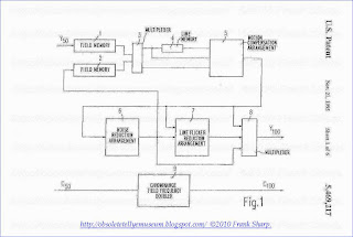 DETAILED DESCRIPTION OF THE PREFERRED EMBODIMENTS OF THE INVENTION
FIG. 1 shows a block diagram of the arrangement according to the invention, which arrangement allows the field frequency of an original picture signal to be doubled and thus generates a converted picture signal, which generated picture signal is noise-reduced, and which performs, if necessary, a motion compensation and a line flicker reduction for the fields.
The arrangement of FIG. 1 is divided into two blocks, the first block processing the received luminance signal component Y50 of the original picture signal and the second block processing the received chrominance signal component C50 of the original picture signal. In the embodiment shown in FIG. 1 the chrominance signal is doubled only with respect to its frequency. The special procedures of noise reduction and line flicker reduction are performed only for the luminance signal in the embodiment shown in FIG. 1. However, it is alternatively possible to take these measures both for the luminance signal and for the chrominance signal.
In the arrangement shown in FIG. 1 the luminance signal component Y50 of the original picture signal is applied to a first field memory 1 by means of which the field frequency of this signal is doubled. Each field of the original picture signal written into the field memory 1 is subsequently read twice. This reading process is performed at the double frequency. A simple doubling of the field frequency is thus already performed. However, the output signal of this field memory is only suitable for display if motion disturbances and line flicker are accepted. Furthermore, a second field memory 2 is provided whose input receives field signals to be described hereinafter, which signals already have the double field frequency. The signals of two consecutive fields of the original picture signal are parallel available at the outputs of the two field memories 1 and 2, which fields have already been doubled in field frequency.
The two field memories 1 and 2 are followed by a multiplexer 3 allowing one of the output signals of the field memories 1 and 2 to be alternatively applied to a line memory 4. The output signals of the two field memories 1 and 2 are applied to a motion compensation arrangement 5 via the multiplexer 3. The arrangement 5 thus receives the signals of the two field memories 1 and 2 and hence two consecutive fields of the original picture signal whose field frequencies have already been doubled. By using the line memory 4, the values of two pixels of the same line position of consecutive picture lines are simultaneously available for one of the two field signals.
The motion compensation arrangement 5 determines, from the two fields apply thereto, a motion which is present in the picture contents between these two fields. Advantageously, a motion vector indicating the motion between the two fields for a group of pixels is obtained from this determined motion for a group of pixels. The motion compensation arrangement 5 can determine this motion both in the horizontal direction and in the vertical direction, i.e. in the line direction as well as in the direction perpendicular to the lines. However, the motion may exclusively be determined in the line direction, which is much easier to realise in the circuit construction and also yields good results.
The arrangement shown in FIG. 1 also includes a noise reduction arrangement 6. This arrangement 6 may operate in known manner in which it combines the signals of pixels of the same location in consecutive fields. These signals are applied from the arrangement 5 to the arrangement 6. Since the arrangement 5 has already determined the corresponding motion vector, the noise reduction in the arrangement 6 can already be performed with motion-compensated signals.
The output signal of the noise reduction arrangement 6 is applied to the input of the second field memory 2, to an input of a line flicker reduction arrangement 7 and to a first input of a multiplexer 8. A signal which is already noise-reduced is thus written into the field memory 2 at the input side, which signal corresponds to that field which is read from the first field memory 1 for the second time already.
The line flicker reduction arrangement 7 which may be, for example a median filter and which selects, from the signals applied thereto, the signal with the middle instantaneous amplitude value, not only receives the output signal from the arrangement 6 but also the output signal from the motion compensation arrangement 5, because this output signal also contains the motion-compensated output signal of the line memory 4. This is necessary because a vertical interpolation must be performed for the line flicker reduction and consequently the pixels corresponding to the signals of two lines should be available, i.e. pixels of the same location in their line.
The line flicker reduction arrangement 7 not only receives these signals of two successive picture lines of a field from the arrangement 6 but also the signal of another field. In a manner to be described hereinafter a median filtering of these signals is performed, which leads to a line flicker reduction.
The output signal of the line flicker reduction arrangement 7 is applied to a second input of the multiplexer 8. A third input of the multiplexer 8 receives the output signal from the noise reduction arrangement 5.
At the output, the multiplexer 8 supplies the luminance signal Y100 which represents the converted picture signal and which has a doubled field frequency as compared with the input signal Y50. In a manner to be described hereinafter, the multiplexer 8 is switched between its three inputs dependent on the field to be generated.
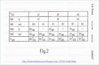 FIG. 1 further shows a circuit block 9 in which the field frequency of the chrominance signal component C50
of the original picture signal is doubled. This can be effected in the
same way as for the luminance signal but alternatively, the field
frequency may be doubled only. At the output, the unit 9 supplies the
chrominance signal component of the converted picture signal.
FIG. 1 further shows a circuit block 9 in which the field frequency of the chrominance signal component C50
of the original picture signal is doubled. This can be effected in the
same way as for the luminance signal but alternatively, the field
frequency may be doubled only. At the output, the unit 9 supplies the
chrominance signal component of the converted picture signal.
FIG. 2 shows a Table indicating diagrammatically which fields are written into or read from the field memories 1 and 2 shown in FIG. 1.
Two consecutive fields of the original picture signal are denoted by A1, B1 and A2, B2, etc. in an unchanged form. Two fields having the same cipher form part of a frame. The two fields are generated in accordance with the interlaced scanning method.
As is shown in the Table of FIG. 2, for example two fields A1 and B1 of a frame of the original picture signal are written into the field memory 1 of FIG. 1, which field memory is denoted by FM1 in FIG. 2. Each of these two fields is subsequently read twice from the field memory 1, which reading is effected at the double frequency so that the field frequency of these pictures is already doubled.
If a field is read from the first field memory 1 for the second time, this signal reaches the input of the field memory 2 denoted by FM2 in the Table of FIG. 2, after it has passed through the arrangement 5 and the arrangement 6 of FIG. 1. At the next reading step of the field memories 1 and 2, two fields whose field frequencies have already been doubled are available at their outputs. As one of the fields, viz. the field written into the field memory 2 has already passed through the noise reduction arrangement, this field is already noise-reduced which is denoted by NR in the Table of FIG. 2.
The result is that two fields from the original picture signal having an already doubled field frequency are available at the outputs of the field memories 1 and 2 in FIG. 1.
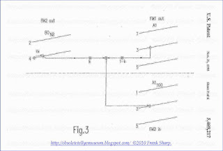 It will now be explained with reference to FIGS. 3 to 6 how the four fields A1100,B1-100,B1*100 and B1+100 of the output signal Y100
as shown in the Table of FIG. 2, which are the signals of the
multiplexer 8 as shown in FIG. 1, are obtained. These four fields are
hereinafter assumed to be associated with a sequence. A frame of the
original picture signal or two fields of this signal, viz. the fields A1
and B1 correspond to this sequence. The four fields of the sequence
will hereinafter be assumed to correspond to these two fields of the
original picture signal.
It will now be explained with reference to FIGS. 3 to 6 how the four fields A1100,B1-100,B1*100 and B1+100 of the output signal Y100
as shown in the Table of FIG. 2, which are the signals of the
multiplexer 8 as shown in FIG. 1, are obtained. These four fields are
hereinafter assumed to be associated with a sequence. A frame of the
original picture signal or two fields of this signal, viz. the fields A1
and B1 correspond to this sequence. The four fields of the sequence
will hereinafter be assumed to correspond to these two fields of the
original picture signal.
FIG. 3 shows diagrammatically, above a broken line, two fields B0NR and A1 of the original picture signal read from the two field memories 1 and 2 of FIG. 1. Below the broken line, a field A1100 is shown which represents the first field of a sequence of the converted picture signal. This signal of the field A1100 is to be generated by the arrangement of FIG. 1.
To this end the output signal of the first field memory 1 is used, from which field memory the field A1 of the original picture signal (at the doubled field frequency) is read. The field B0 of the original picture signal was already previously written in a noise-reduced form into the field memory 2. At the output, this signal is now available as signal B0NR at the output of the second field memory simultaneously with the signal A1. The first field A1100 of the sequence is obtained from these two output signals of the field memories 1 and 2 in accordance with the diagrammatic representation in FIG. 3.
This field A1100 to be generated has the correct position vertically and with respect to time as compared with the field A1 of the original picture signal. Therefore, only a noise reduction should be carried out, and a line flicker reduction in particular is not necessary.
The output signals of the field memories 1 and 2 are utilized for the noise reduction, while it is advantageous to submit the field read from the field memory 2 and not having the correct position with respect to time as compared with the field A1100 to be generated to a motion compensation of its picture contents. The motion vector determined by the motion compensation arrangement 5 in accordance with FIG. 1 is utilized for this purpose. This motion vector is denoted by vx in FIG. 3.
For a pixel marked in picture line 3 of the field A1100 in FIG. 3, the pixel of the same line position and the same line number of the field A1100, as read from the field memory 1, is utilized. Moreover, the pixel of the field B0NR as read from the second field memory and offset by the motion vector vx is used. This pixel is taken from line 4. A noise-reduced signal is obtained from these two pixels of the two fields. A factor k is provided for this purpose, indicating the degree of noise reduction. The pixel from the field A1 is multiplied by a factor 1-k and the pixel from the field B0NR is multiplied by a factor k. These two multiplied values are added and constitute the value of the marked pixel of the field A1100.
If k is chosen to be small, only a small or no noise reduction is to be performed and this pixel is essentially obtained from the corresponding pixel of the field A1. With a larger factor k, the value of the pixel is increasingly being taken from the field B0NR.
The generated field A1100 thus corresponds to the field A1 of the original picture signal, but for the performed noise reduction. It is written into the second field memory 2 of FIG. 1 and is available as A1NR for subsequent fields to be generated.
During the generation of the first field A1100 the multiplexer 8 is switched to its first input in accordance with FIG. 1, because the output signals for the noise reduction are used as output signals in accordance with the diagrammatic representation in FIG. 3 and hence as signals for the field A1100.
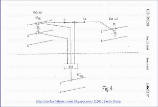 FIG. 4 is a representation, corresponding to FIG. 3, for obtaining the second field B1-100 of the sequence.
As compared with the two fields of the original picture signal, this second field of the sequence neither has a vertically correct position nor a correct position as regards time. Therefore, a motion compensation and a line flicker reduction are performed.
At the instant of generating this second field, the field B1 of the original picture signal is read from the first field memory and the field A1 of the original picture signal is read in a noise-reduced form from the second field memory.
In the representation in FIG. 4 a pixel of the picture line 2 is marked for the field B1-100. The value of this pixel is generated from three values by means of median filtering, which values are obtained from the fields A1NR and B1.
The first of these values is obtained from the picture line 3 for that pixel which, after being offset by half the motion vector (vx.1/2) has the same position as the pixel to be generated in the field B1-100. The second input signal of the median filter is obtained from the pixel of the same line position of line 1 of the field A1NR. The value of this pixel is also multiplied by a factor k. Moreover, that pixel of the picture line 2 of the field B1 which, after use of half the negative motion vector (-vx.1/2) has the same picture line position as the pixel to be generated of the field B1-100 is multiplied by a factor 1-k. These two values are added and the sum constitutes the third input signal for the median filtering. Due to the median filtering, the input signal having the middle instantaneous amplitude value is selected from these three input signals. This signal is constituted by the value of the marked pixel of the second field B1-100 of the sequence.
As already shown in the representation according to FIG. 4, a motion compensation for all signals is required for this field. Moreover, a line flicker reduction is to be performed. Consequently, the multiplexer 8 is switched to its second input for generating the value of the field B1-100 in accordance with the representation in FIG. 1, which input receives the output signal from the line flicker reduction arrangement 7.
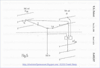 FIG. 5 is a representation corresponding to FIGS. 3 and 4, but in the representation according to FIG. 5 the third field B1*100 of the sequence is to be generated.
The two corresponding fields A1 and B1 of the original picture signal are used again for generating this field. The field B1 is read from the field memory 1 of FIG. 1. The field A1, which is already noise-reduced, is read from the field memory 2 of FIG. 1.
A median filtering is performed again, because the output field B1 has the incorrect vertical position. The output field A1NR additionally has the incorrect position with respect to time so that also a motion compensation has to be performed for this field.
A median filtering of three input signals is carried out for generating one of the pixels marked in FIG. 5, of the picture line 3 of the field B1*100.
The first of these input signals represents the value of the pixel of the picture line 2 of the field B1, which has the same picture line position in its picture line as the pixel to be generated in its picture line. Moreover, from the field A1, as read from the second field memory, that pixel is used which after correction by the motion vector vx has the same line position as the pixel to be generated. This motion-compensated pixel represents the second input signal of the median filter. The third input signal is formed by the sum of the value of the same line position of the pixel of the picture line 4 of the field B1, multiplied by a factor 1-k, and the value of the second input signal of the median filter, multiplied by a factor k. This sum represents the third input signal of the median filter and is simultaneously written as input signal into the second field memory from which it can be read again for fields to be subsequently generated.
The multiplexer 8 of the block diagram in FIG. 1 is switched to its second input for generating the third field B1*100 of the sequence, because a line flicker reduction as well as a motion compensation have to be performed.
In FIG. 6, corresponding to the representations in FIGS. 3 to 5, the values of the fourth field B1+100 of the sequence are to be obtained.
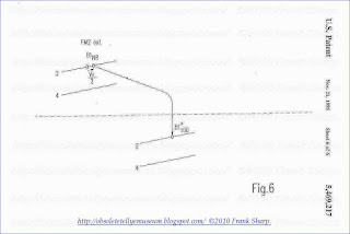 Since
the field B1 used for this purpose (in a noise-reduced form) of the
original picture signal has the correct vertical position, i.e. the same
position as the field B1+100, a line flicker reduction is not necessary in this case. The field B1NR has, however, the incorrect position with respect to time so that a motion compensation is necessary.
Since
the field B1 used for this purpose (in a noise-reduced form) of the
original picture signal has the correct vertical position, i.e. the same
position as the field B1+100, a line flicker reduction is not necessary in this case. The field B1NR has, however, the incorrect position with respect to time so that a motion compensation is necessary.
Consequently, for a pixel as marked by way of example in FIG. 6 in picture line 2 in a given position, that pixel of the field B1NR as read from the field memory 2 is used which has the same line position as the pixel to be generated in its picture line after correction by half the motion vector (vx.1/2).
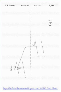 Since only a motion compensation (in
addition to noise reduction) is necessary in this case, the multiplexer
8 of FIG. 1 is switched to its third input.
Since only a motion compensation (in
addition to noise reduction) is necessary in this case, the multiplexer
8 of FIG. 1 is switched to its third input.
The way of generating a sequence of four fields in accordance with FIGS. 3 to 6 is continuously repeated, with four corresponding fields of the converted picture signal being obtained for two output fields of the original picture signal.
The invention relates to an arrangement for converting an original picture signal representing a sequence of frames, each of which is composed of two interlaced fields, into a converted picture signal which has a double field frequency with respect to the original picture signal.
When converting a picture signal into such a converted picture signal which, with respect to the original picture signal, has a double field frequency, there is the problem that every second field of the converted picture signal must be newly generated, because no corresponding field of the original picture signal is available with respect to time and also with respect to the picture information.
In simple arrangements for doubling the field frequency, every field is doubled. A moving object in the fields of the converted picture signal is imaged twice in the same position before it jumps to the next position in the two subsequent fields. Since the human eye cannot follow these jumps, it is incident on the average speed of motion and observes a moving object from field to field at different positions. This leads to a double structure and motion blurr.
In other arrangements for field doubling of a picture signal a motion compensation is therefore provided by means of which the motion between two fields of the original picture signal is determined so that the motion can be taken into account in fields of the converted picture signal to be generated therebetween as a function of time and a corresponding interpolation can be performed. However, such arrangements have the further problem that possibly present noise is also to be reduced and that the line flicker, which still occurs in spite of the doubling of the field frequency in picture signals generated by way of interlaced scanning, is to be reduced. In the state of the art arrangements are only known in which a motion compensation is combined either with a noise reduction or with a line flicker reduction.
SUMMARY OF THE INVENTION
It is an object of the invention to provide an arrangement in which the motion of the picture contents during generation of the compensated fields is taken into account when converting the picture signal into a converted picture signal at the double field frequency, and which moreover allows a noise reduction of the picture signal and a line flicker reduction.
According to the invention this object is solved in that for doubling the field frequency a memory arrangement is provided which precedes an arrangement for motion compensation whose output signal is applied to an arrangement for noise reduction, in that an arrangement for line flicker reduction is provided which receives the output signals from the noise reduction arrangement and the motion compensation arrangement and in that the converted picture signal is obtained from the output signal of the noise reduction arrangement, the line flicker reduction arrangement or the motion compensation arrangement, dependent on the position with respect to time of a field to be generated of the converted picture signal.
The actual the field frequency doubling is obtained by means of a memory arrangement. Consequently, the fields of the original picture signal are repeated at the double frequency so that a double field frequency is realised. However, this signal still has the above-mentioned errors.
An arrangement for motion compensation is therefore provided, which arrangement determines motions in the original picture signal and, with reference to the known motions, allows a compensation of this motion in the new fields to be generated of the compensated signal.
The arrangement for motion compensation precedes an arrangement for noise reduction which combines the data of two consecutive fields for the purpose of noise reduction.
Furthermore, an arrangement for line flicker reduction is provided which receives the output signals from the motion compensation arrangement and the output signals from the noise reduction arrangement.
The output signal of the arrangement, i.e. the converted picture signal of the double field frequency, is obtained from the output signal of one of said three arrangements in dependence upon the position with respect to time of a field to be generated of the converted picture signal. This alternation between the output signals of the arrangements is advantageous because different errors occur, dependent on the position with respect to time of the fields of the converted picture signal. In some fields a motion compensation is required because these fields occur with respect to time between two fields of the original picture signal. This is not required for those fields which coincide with pictures of the original picture signal. The line flicker reduction is in its turn only required for those fields which as a consequence of the interlaced scanning method do not have the correct vertical position as compared with the fields of the original picture signal from which they are generated.
The arrangement according to the invention thus offers a combination of motion compensation with line flicker reduction and noise reduction.
An embodiment of the arrangement is characterized in that the original picture signal is written into a first field memory from which it is read at the double frequency, each field being consecutively read twice, and in that a second field memory is provided into which each field read for the second time from the first field memory is written after it has passed through the noise reduction arrangement.
The first field memory is thus used for doubling the field frequency. Each field written into this memory is read twice consecutively. A second field memory already operates at this double field frequency at the input side, because each field, which was read from the first field memory for the second time and has passed through the noise reduction arrangement, is written into this second field memory. After this noise-reduced field has been written into the memory, it is available at the output of the second field memory.
Consequently, two fields of the original picture signal, however, with a doubled field frequency are available at the outputs of the two field memories for the motion compensation arrangement. One of these fields is already noise-reduced, which simplifies the determination of motion by the motion compensation arrangement.
A further embodiment of the invention is characterized in that the two field memories precede a line memory which buffers a picture line of one of the output signals of the two fields. For one of the fields information of two consecutive picture lines is thus time-parallel available, which is advantageous for the subsequent line flicker reduction.
In a further embodiment of the invention the arrangement for line flicker reduction may advantageously be a median filter whose output supplies that input signal which has the middle amplitude value of the input signals.
In accordance with a further embodiment of the invention the arrangement for motion compensation receives the output signals of the two field memories and the line memory, which motion compensation arrangement determines a motion vector from the two consecutive fields of the original picture signal read from the field memories, which motion vector indicates the motion between the two fields for a group of pixels of these fields.
This motion vector may be used for motion compensation in those fields of the converted field signal which occur with respect to time between two fields of the original picture signal.
A further embodiment of the invention is characterized in that the arrangement generates a sequence of four fields (A1100,B1-100,B1*100,B1+100) of the converted picture signal corresponding to two fields of a frame of the original picture signal, the first field (A1100) of the sequence being obtained from the output signal of the noise reduction arrangement, the second and third fields (B1-100,B1*100) of the sequence being obtained from the output signal of the line flicker reduction arrangement and the fourth field (B1+100) of the sequence being obtained from the motion compensation arrangement.
As a consequence of the doubled field frequency of the converted picture signal, four fields of the converted picture signal must be generated in a time range in which two fields of the original picture signal are present. These two fields of the original picture signal and the four fields of the corresponding sequence of the converted picture signal will hereinafter be referred to as corresponding fields and corresponding sequence, respectively.
The first field of the sequence is obtained from the output signal of the noise reduction arrangement. This is possible because this first field of the sequence has the right position with respect to time and location as compared with the first corresponding field of the original picture signal and because only a noise reduction is to be performed.
The second and third fields of the sequence are obtained from the output signal of the line flicker reduction arrangement, because the two fields of the original picture signal must be utilized for these two fields, at least one of which does not have the correct position with respect to time and neither has the correct vertical position due to the interlaced scanning method used.
The signal for the fourth field of the sequence is obtained from the motion compensation arrangement, because this signal can only be obtained from the second corresponding field of the original picture signal due to use of motion compensation.
The further sub-claims state how the arrangement advantageously generates the four fields for the sequence of converted picture signals from the corresponding two fields of the original picture signal.
These and other aspects of the invention will be apparent from and elucidated with reference to the embodiments described hereinafter.
BRIEF DESCRIPTION OF THE DRAWINGS
FIG. 1 shows a block diagram of the arrangement according to the invention for converting an original picture signal into a converted picture signal of the double field frequency,
FIG. 2 shows a Table of the fields written into and read from the memory arrangement according to FIG. 1,
FIG. 3 shows a diagram in accordance with which the arrangement of FIG. 1 generates the first field of a sequence of the converted picture signal,
FIG. 4 is a representation, corresponding to FIG. 3, of the second field of the sequence,
FIG. 5 is a representation, corresponding to FIG. 3, of the third field of the sequence, and
FIG. 6 is a representation, corresponding to FIG. 3, of the fourth field of the sequence.
 DETAILED DESCRIPTION OF THE PREFERRED EMBODIMENTS OF THE INVENTION
FIG. 1 shows a block diagram of the arrangement according to the invention, which arrangement allows the field frequency of an original picture signal to be doubled and thus generates a converted picture signal, which generated picture signal is noise-reduced, and which performs, if necessary, a motion compensation and a line flicker reduction for the fields.
The arrangement of FIG. 1 is divided into two blocks, the first block processing the received luminance signal component Y50 of the original picture signal and the second block processing the received chrominance signal component C50 of the original picture signal. In the embodiment shown in FIG. 1 the chrominance signal is doubled only with respect to its frequency. The special procedures of noise reduction and line flicker reduction are performed only for the luminance signal in the embodiment shown in FIG. 1. However, it is alternatively possible to take these measures both for the luminance signal and for the chrominance signal.
In the arrangement shown in FIG. 1 the luminance signal component Y50 of the original picture signal is applied to a first field memory 1 by means of which the field frequency of this signal is doubled. Each field of the original picture signal written into the field memory 1 is subsequently read twice. This reading process is performed at the double frequency. A simple doubling of the field frequency is thus already performed. However, the output signal of this field memory is only suitable for display if motion disturbances and line flicker are accepted. Furthermore, a second field memory 2 is provided whose input receives field signals to be described hereinafter, which signals already have the double field frequency. The signals of two consecutive fields of the original picture signal are parallel available at the outputs of the two field memories 1 and 2, which fields have already been doubled in field frequency.
The two field memories 1 and 2 are followed by a multiplexer 3 allowing one of the output signals of the field memories 1 and 2 to be alternatively applied to a line memory 4. The output signals of the two field memories 1 and 2 are applied to a motion compensation arrangement 5 via the multiplexer 3. The arrangement 5 thus receives the signals of the two field memories 1 and 2 and hence two consecutive fields of the original picture signal whose field frequencies have already been doubled. By using the line memory 4, the values of two pixels of the same line position of consecutive picture lines are simultaneously available for one of the two field signals.
The motion compensation arrangement 5 determines, from the two fields apply thereto, a motion which is present in the picture contents between these two fields. Advantageously, a motion vector indicating the motion between the two fields for a group of pixels is obtained from this determined motion for a group of pixels. The motion compensation arrangement 5 can determine this motion both in the horizontal direction and in the vertical direction, i.e. in the line direction as well as in the direction perpendicular to the lines. However, the motion may exclusively be determined in the line direction, which is much easier to realise in the circuit construction and also yields good results.
The arrangement shown in FIG. 1 also includes a noise reduction arrangement 6. This arrangement 6 may operate in known manner in which it combines the signals of pixels of the same location in consecutive fields. These signals are applied from the arrangement 5 to the arrangement 6. Since the arrangement 5 has already determined the corresponding motion vector, the noise reduction in the arrangement 6 can already be performed with motion-compensated signals.
The output signal of the noise reduction arrangement 6 is applied to the input of the second field memory 2, to an input of a line flicker reduction arrangement 7 and to a first input of a multiplexer 8. A signal which is already noise-reduced is thus written into the field memory 2 at the input side, which signal corresponds to that field which is read from the first field memory 1 for the second time already.
The line flicker reduction arrangement 7 which may be, for example a median filter and which selects, from the signals applied thereto, the signal with the middle instantaneous amplitude value, not only receives the output signal from the arrangement 6 but also the output signal from the motion compensation arrangement 5, because this output signal also contains the motion-compensated output signal of the line memory 4. This is necessary because a vertical interpolation must be performed for the line flicker reduction and consequently the pixels corresponding to the signals of two lines should be available, i.e. pixels of the same location in their line.
The line flicker reduction arrangement 7 not only receives these signals of two successive picture lines of a field from the arrangement 6 but also the signal of another field. In a manner to be described hereinafter a median filtering of these signals is performed, which leads to a line flicker reduction.
The output signal of the line flicker reduction arrangement 7 is applied to a second input of the multiplexer 8. A third input of the multiplexer 8 receives the output signal from the noise reduction arrangement 5.
At the output, the multiplexer 8 supplies the luminance signal Y100 which represents the converted picture signal and which has a doubled field frequency as compared with the input signal Y50. In a manner to be described hereinafter, the multiplexer 8 is switched between its three inputs dependent on the field to be generated.
 FIG. 1 further shows a circuit block 9 in which the field frequency of the chrominance signal component C50
of the original picture signal is doubled. This can be effected in the
same way as for the luminance signal but alternatively, the field
frequency may be doubled only. At the output, the unit 9 supplies the
chrominance signal component of the converted picture signal.
FIG. 1 further shows a circuit block 9 in which the field frequency of the chrominance signal component C50
of the original picture signal is doubled. This can be effected in the
same way as for the luminance signal but alternatively, the field
frequency may be doubled only. At the output, the unit 9 supplies the
chrominance signal component of the converted picture signal. FIG. 2 shows a Table indicating diagrammatically which fields are written into or read from the field memories 1 and 2 shown in FIG. 1.
Two consecutive fields of the original picture signal are denoted by A1, B1 and A2, B2, etc. in an unchanged form. Two fields having the same cipher form part of a frame. The two fields are generated in accordance with the interlaced scanning method.
As is shown in the Table of FIG. 2, for example two fields A1 and B1 of a frame of the original picture signal are written into the field memory 1 of FIG. 1, which field memory is denoted by FM1 in FIG. 2. Each of these two fields is subsequently read twice from the field memory 1, which reading is effected at the double frequency so that the field frequency of these pictures is already doubled.
If a field is read from the first field memory 1 for the second time, this signal reaches the input of the field memory 2 denoted by FM2 in the Table of FIG. 2, after it has passed through the arrangement 5 and the arrangement 6 of FIG. 1. At the next reading step of the field memories 1 and 2, two fields whose field frequencies have already been doubled are available at their outputs. As one of the fields, viz. the field written into the field memory 2 has already passed through the noise reduction arrangement, this field is already noise-reduced which is denoted by NR in the Table of FIG. 2.
The result is that two fields from the original picture signal having an already doubled field frequency are available at the outputs of the field memories 1 and 2 in FIG. 1.
 It will now be explained with reference to FIGS. 3 to 6 how the four fields A1100,B1-100,B1*100 and B1+100 of the output signal Y100
as shown in the Table of FIG. 2, which are the signals of the
multiplexer 8 as shown in FIG. 1, are obtained. These four fields are
hereinafter assumed to be associated with a sequence. A frame of the
original picture signal or two fields of this signal, viz. the fields A1
and B1 correspond to this sequence. The four fields of the sequence
will hereinafter be assumed to correspond to these two fields of the
original picture signal.
It will now be explained with reference to FIGS. 3 to 6 how the four fields A1100,B1-100,B1*100 and B1+100 of the output signal Y100
as shown in the Table of FIG. 2, which are the signals of the
multiplexer 8 as shown in FIG. 1, are obtained. These four fields are
hereinafter assumed to be associated with a sequence. A frame of the
original picture signal or two fields of this signal, viz. the fields A1
and B1 correspond to this sequence. The four fields of the sequence
will hereinafter be assumed to correspond to these two fields of the
original picture signal. FIG. 3 shows diagrammatically, above a broken line, two fields B0NR and A1 of the original picture signal read from the two field memories 1 and 2 of FIG. 1. Below the broken line, a field A1100 is shown which represents the first field of a sequence of the converted picture signal. This signal of the field A1100 is to be generated by the arrangement of FIG. 1.
To this end the output signal of the first field memory 1 is used, from which field memory the field A1 of the original picture signal (at the doubled field frequency) is read. The field B0 of the original picture signal was already previously written in a noise-reduced form into the field memory 2. At the output, this signal is now available as signal B0NR at the output of the second field memory simultaneously with the signal A1. The first field A1100 of the sequence is obtained from these two output signals of the field memories 1 and 2 in accordance with the diagrammatic representation in FIG. 3.
This field A1100 to be generated has the correct position vertically and with respect to time as compared with the field A1 of the original picture signal. Therefore, only a noise reduction should be carried out, and a line flicker reduction in particular is not necessary.
The output signals of the field memories 1 and 2 are utilized for the noise reduction, while it is advantageous to submit the field read from the field memory 2 and not having the correct position with respect to time as compared with the field A1100 to be generated to a motion compensation of its picture contents. The motion vector determined by the motion compensation arrangement 5 in accordance with FIG. 1 is utilized for this purpose. This motion vector is denoted by vx in FIG. 3.
For a pixel marked in picture line 3 of the field A1100 in FIG. 3, the pixel of the same line position and the same line number of the field A1100, as read from the field memory 1, is utilized. Moreover, the pixel of the field B0NR as read from the second field memory and offset by the motion vector vx is used. This pixel is taken from line 4. A noise-reduced signal is obtained from these two pixels of the two fields. A factor k is provided for this purpose, indicating the degree of noise reduction. The pixel from the field A1 is multiplied by a factor 1-k and the pixel from the field B0NR is multiplied by a factor k. These two multiplied values are added and constitute the value of the marked pixel of the field A1100.
If k is chosen to be small, only a small or no noise reduction is to be performed and this pixel is essentially obtained from the corresponding pixel of the field A1. With a larger factor k, the value of the pixel is increasingly being taken from the field B0NR.
The generated field A1100 thus corresponds to the field A1 of the original picture signal, but for the performed noise reduction. It is written into the second field memory 2 of FIG. 1 and is available as A1NR for subsequent fields to be generated.
During the generation of the first field A1100 the multiplexer 8 is switched to its first input in accordance with FIG. 1, because the output signals for the noise reduction are used as output signals in accordance with the diagrammatic representation in FIG. 3 and hence as signals for the field A1100.
 FIG. 4 is a representation, corresponding to FIG. 3, for obtaining the second field B1-100 of the sequence.
 As compared with the two fields of the original picture signal, this second field of the sequence neither has a vertically correct position nor a correct position as regards time. Therefore, a motion compensation and a line flicker reduction are performed.
At the instant of generating this second field, the field B1 of the original picture signal is read from the first field memory and the field A1 of the original picture signal is read in a noise-reduced form from the second field memory.
In the representation in FIG. 4 a pixel of the picture line 2 is marked for the field B1-100. The value of this pixel is generated from three values by means of median filtering, which values are obtained from the fields A1NR and B1.
The first of these values is obtained from the picture line 3 for that pixel which, after being offset by half the motion vector (vx.1/2) has the same position as the pixel to be generated in the field B1-100. The second input signal of the median filter is obtained from the pixel of the same line position of line 1 of the field A1NR. The value of this pixel is also multiplied by a factor k. Moreover, that pixel of the picture line 2 of the field B1 which, after use of half the negative motion vector (-vx.1/2) has the same picture line position as the pixel to be generated of the field B1-100 is multiplied by a factor 1-k. These two values are added and the sum constitutes the third input signal for the median filtering. Due to the median filtering, the input signal having the middle instantaneous amplitude value is selected from these three input signals. This signal is constituted by the value of the marked pixel of the second field B1-100 of the sequence.
As already shown in the representation according to FIG. 4, a motion compensation for all signals is required for this field. Moreover, a line flicker reduction is to be performed. Consequently, the multiplexer 8 is switched to its second input for generating the value of the field B1-100 in accordance with the representation in FIG. 1, which input receives the output signal from the line flicker reduction arrangement 7.
 FIG. 5 is a representation corresponding to FIGS. 3 and 4, but in the representation according to FIG. 5 the third field B1*100 of the sequence is to be generated.
 The two corresponding fields A1 and B1 of the original picture signal are used again for generating this field. The field B1 is read from the field memory 1 of FIG. 1. The field A1, which is already noise-reduced, is read from the field memory 2 of FIG. 1.
A median filtering is performed again, because the output field B1 has the incorrect vertical position. The output field A1NR additionally has the incorrect position with respect to time so that also a motion compensation has to be performed for this field.
A median filtering of three input signals is carried out for generating one of the pixels marked in FIG. 5, of the picture line 3 of the field B1*100.
The first of these input signals represents the value of the pixel of the picture line 2 of the field B1, which has the same picture line position in its picture line as the pixel to be generated in its picture line. Moreover, from the field A1, as read from the second field memory, that pixel is used which after correction by the motion vector vx has the same line position as the pixel to be generated. This motion-compensated pixel represents the second input signal of the median filter. The third input signal is formed by the sum of the value of the same line position of the pixel of the picture line 4 of the field B1, multiplied by a factor 1-k, and the value of the second input signal of the median filter, multiplied by a factor k. This sum represents the third input signal of the median filter and is simultaneously written as input signal into the second field memory from which it can be read again for fields to be subsequently generated.
The multiplexer 8 of the block diagram in FIG. 1 is switched to its second input for generating the third field B1*100 of the sequence, because a line flicker reduction as well as a motion compensation have to be performed.
In FIG. 6, corresponding to the representations in FIGS. 3 to 5, the values of the fourth field B1+100 of the sequence are to be obtained.
 Since
the field B1 used for this purpose (in a noise-reduced form) of the
original picture signal has the correct vertical position, i.e. the same
position as the field B1+100, a line flicker reduction is not necessary in this case. The field B1NR has, however, the incorrect position with respect to time so that a motion compensation is necessary.
Since
the field B1 used for this purpose (in a noise-reduced form) of the
original picture signal has the correct vertical position, i.e. the same
position as the field B1+100, a line flicker reduction is not necessary in this case. The field B1NR has, however, the incorrect position with respect to time so that a motion compensation is necessary. Consequently, for a pixel as marked by way of example in FIG. 6 in picture line 2 in a given position, that pixel of the field B1NR as read from the field memory 2 is used which has the same line position as the pixel to be generated in its picture line after correction by half the motion vector (vx.1/2).
 Since only a motion compensation (in
addition to noise reduction) is necessary in this case, the multiplexer
8 of FIG. 1 is switched to its third input.
Since only a motion compensation (in
addition to noise reduction) is necessary in this case, the multiplexer
8 of FIG. 1 is switched to its third input. The way of generating a sequence of four fields in accordance with FIGS. 3 to 6 is continuously repeated, with four corresponding fields of the converted picture signal being obtained for two output fields of the original picture signal.
SAA4996H Motion Adaptive Colour Plus And Control IC (MACPACIC) for PALplus:
1 FEATURES
· Motion adaptive colour plus decoding
· Helper AGC/AOC
· Help
er decompanding· Memory controlling
· VERIC controlling.
2 GENERAL DESCRIPTION
The SAA4996H (MACPACIC) performs the Motion
Adaptive Colour Plus (MACP) processing which is a
dedicated field comb filter technique exploited for the
PALplus system.
The integrated circuit is especially designed to be used in
conjunction with the SAA4997H Vertical Reconstruction IC
(VERIC) to decode the transmitted PALplus video signals
in PALplus colour TV receivers.
In addition, a hardware configuration ‘stand-alone
MACPACIC’ with only two field memories (FM1 and FM4)
is also possible. In this condition no helper lines are
processed and no vertical reconstruction is applied.
This configuration enables the Motion Adaptive Colour
Plus processing to be performed in non PALplus receivers.
FUNCTIONAL DESCRIPTION
7.1 Introduction
The MACPACIC is designed to be used in the PALplus
decoder module of a PALplus colour TV receiver. The full
PALplus decoder module consists of two special
integrated circuits and four field memories, as illustrated in
Fig.5.
The special ICs are as follows;
· Motion Adaptive Colour Plus And Control IC
(MACPACIC) for PALplus (SAA4996H)
· Vertical Reconstruction IC (VERIC) (SAA4997H).
Besides the full PALplus module, a configuration for
stand-alone Motion Adaptive Colour Plus processing
(MACP) is also possible (see Fig.6). In this event only
MACPACIC with FM1 and FM4 are necessary.
This configuration enables the MACP processing in
non-PALplus receivers to be performed.
The PALplus module is designed to operate in conjunction
with a 100 Hz feature box. All special requirements such
as the delay of the PALplus module, bypass modes and
generation of the necessary control and clock signals will
be fulfilled.
7.1.1 DATA PROCESSING
The MACPACIC includes the decompanding functions for
the helper lines and the motion adaptive
luminance/chrominance separation in accordance with the
PALplus system description REV. 3.0 with some
modifications;
· The system operates at a clock frequency of 16 MHz
· The Y:U:V format is 4:1:1 instead of 4:2:2
· The filter DEC_MD_UV_LPF is not implemented
· If noisy helper signals are received, the helper
bandwidth and/or amplitude can be reduced
· Automatic gain control of the helper signal with respect
to the luminance signal.
The input signals are the BB(helper)/CVBS and
chrominance signals which are derived from the
analog-to-digital converter (ADC).
At its outputs the MACPACIC delivers separate luminance
and chrominance signals, each one free from
cross-artefacts as main signal, as well as decompanded
and filtered helper signals. For standard input signals and,
in the event of MultiPIP mode with the help of a
PIP module, the MACPACIC can be switched to different
bypass modes.
7.1.2 CONTROL
Memory control, PALplus system controlling and clock
generation (from the incoming 16 MHz and 32 MHz
line-locked clocks) are implemented in the MACPACIC.
All clocks and control signals necessary for the PALplus
module (excluding read control of FM2/FM3) are
generated in the controller part. Inputs are reference
signals, clocks and control signals delivered by the
colour/helper decoder IC (TDA9144), and the 100 Hz
memory controller, i.e. ECO4 (SAA4952) or ECOBENDIC
(SAA4970). The MACPACIC also receives control
information via a three-wire serial interface (SNERT-bus)
from the microprocessor in the 100 Hz feature box.
7.2 General requirements
The PALplus IC set is designed to operate in conjunction
with the PHILIPS 100 Hz feature box. All requirements
with respect to this combination are fulfilled.
The special requirements are as follows;
· The signal processing is adapted to the analog
preprocessing in the TDA9144 for luminance, helper
and chrominance signals
· Clock rate and clock generation
· Some special control signals are generated in the
PALplus module
· The field length must be measured and used to set the
delay of the full PALplus module to 1.5 fields
· A SNERT interface is used to transfer control data to
and from the PALplus module
· MultiPIP with the help of a PIP module is possible
· Results of noise measurements influence the helper
processing
· Automatic gain and offset control is implemented
· Reference signals in line 22 are used for inverse set-up
operation
· Noise measurement implemented
· Boundary scan test implemented
· Preset of internal recursive parts for testing.
7.3 Hardware configurations and delays
Two general hardware configurations are possible.
7.3.1 FULL PALPLUS MODULE (see Fig.5)
The delay from input to output is 1.5 fields rounded to
complete lines, also in the bypass mode. Therefore, the
number of input lines of the odd and even fields must be
measured. The result of this measurement is then used to
generate the required delay.
In the MultiPIP mode the delay of the full PALplus module
is one line.
7.3.2 STAND-ALONE MACPACIC (see Fig.6)
In this situation only the MACPACIC with FM1 and FM4
are necessary. No helper lines are processed and no
vertical reconstruction with the VERIC is applied.
The delay from input to output is one field, one line and
some clocks of processing delay, this also applies in the
bypass mode. In the MultiPIP mode the delay is two clocks
(CLK_16).
7.4 Analog processing in front of the PALplus
module
In front of the MACPACIC an analog colour/helper
decoder (TDA9144) performs the colour and helper
demodulation.
Because of the requirement that a standard ADC with
clamping on 16 should be used for CVBS and helper
analog-to-digital conversion, a black (letter box lines) and
mid grey (helper lines) shift is applied in the colour/helper
decoder. For reshifting without errors in the digital domain
these shift levels are inserted as
a reference in line 22.In the event of stand-alone MACPACIC and PALplus input
signals the helper demodulation must be switched off.
No special actions are taken in the colour/helper decoder
for chrominance processing.
In this document U will refer to -(B - Y) and V will refer to
-(R - Y).
In combination with the full PALplus module with letter box
input signals (16:9), the PAL delay line of the colour/helper
decoder must be switched off. This is because this function
is also implemented in the vertical reconstruction filter of
the VERIC. For all other input signals and for stand-alone
MACPACIC the PAL delay line must be switched on.
The device consists of
4 main parts:
· Luminance and helper processing
· Chrominance processing
· Chrominance motion detection
· Control.
The clock rate of the input data is 16 MHz. Internally, the
device operates at a 32 MHz clock frequency. The clock
rate of the output data is either 32 MHz (in combination
with FM2, FM3 and VERIC) or 16 MHz for stand-alone
MACP processing.
The delay of the full PALplus module is 1.5 fields in the
PALplus and bypass mode. A field length measurement is
implemented. For MultiPIP with the help of a PIP module
the delay of the PALplus module is one line.
For stand-alone MACP the delay is one field, one line and
some clocks of processing delay.
For MultiPIP with the help of a PIP module the delay of
MACPACIC is two clocks (CLK_16).
7.6 Luminance and helper processing
7.6.1 INPUT RANGE
To use a standard ADC with clamping on 16, a black
set-up for the CVBS signal and a black/mid grey set-up for
the helper signal has to be performed in the colour/helper
decoder. The shift values for black set-up and mid grey
set-up are inserted in line 22.
All values are nominal values.
CVBS:
clamp level: 16
black set-up: 51
white: 191
format: 8-bit, straight binary
Helper:
mid grey set-up: 121
range: (121 - 60) to (121 + 60) = 61 to 181
format: 8-bit, offset binary
Y (standard input):
black: 16
peak white: 191
format: 8-bit, straight binary
7.7 Luminance processing
The luminance and the helper processing have two input
branches. One input is an 8-bit wide 16 MHz data stream
from the ADC. The other is an 8-bit wide 16 MHz data
stream from the field memory (FM1). The odd field of an
input frame is stored in the field memory FM1. In the even
field of a frame, the even field together with the delayed
odd field is processed by the MACPACIC.
To remove the chrominance part of the incoming
composite video signal, the Motion Adaptive Colour Plus
technique is applied. Colour Plus is a dedicated comb filter
technique, which makes full use of the correlation of two
successive fields.
During processing the data of the odd and even fields are
separated in a high-pass and low-pass part. The high-pass
part consists of the luminance high-pass component and
the modulated chrominance signal. Due to the phase
difference of the colour carrier of 180° from the odd to the
even field, the chrominance signal can be removed by
adding the high-pass signals.
This processing will work successfully in the film mode,
because scanned film material is motionless within the two
fields of one frame. In the camera mode a motion detector
fades down the luminance high-pass component if motion
is detected.
The following vertical low-pass filters perform a vertical
interpolation of the high-pass part by the factor of two.
In the event of bad signal conditions, the residual
cross-luminance signal, caused by clock jitter between two
fields, can be reduced by using this filter as a 2D comb
filter. Therefore different sets of coefficients can be
selected via SNERT.
The luminance high-pass part and the luminance low-pass
part are then added.
The automatic gain control (AGC) and automatic offset
control (AOC) functions use reference lines 23,
623 and 22 to reduce errors in the vertical reconstruction
in the VERIC. This is to reduce the effects of any errors
that might be caused due to variations in the conventional
PAL references in the signal during the transmission chain
with respect to the levels of the luminance letter box and
helper signals.
LUMINANCE HELPER PROCESSING
In the event of incoming helper, the switchable low-pass
filter acts as an inverse shaping and bandwidth reduction
filter for the helper lines. If a distorted helper signal is
transmitted, the bandwidth can be reduced from 2.2 MHz
(0 dB) to 1.0 MHz or to 0.5 MHz (-3 dB).
The high-pass part of the luminance processing is not
used for the helper processing.
To stabilize the transmitted helper signal against noise
disturbances, the encoder performs a companding of the
signal. In the decoder the decompanding is performed in
the AGOC block (see Fig.7).
7.8 Output signals
In the event of full PALplus configuration, odd and even
field data are multiplexed to a 32 MHz data stream.
For the stand-alone MACPACIC, the processed even field
data is connected to the field memory FM1 and the odd
field data is switched to the output Y_MA. In the next field
the stored even field data is read out of the field memory
FM1 and then connected to the output of the MACPACIC.
If MultiPIP mode is selected, the luminance input data from
the ADC (Y_ADC) is switched directly to the output Y_MA.
In the bypass mode the luminance data processing is
switched off and multiplexed data is connected to the
MACPACIC output.
The clock frequency of the output data Y_MA is 32 MHz for
the MACPACIC in combination with the VERIC, or 16 MHz
for the stand-alone MACPACIC.
7.9 Measurements
The digital data stream at the input of the PALplus decoder
module contains three reference lines;
· Reference line 22 consists of the black and mid grey
set-up, inserted by the colour/helper decoder
· The second half of line 23 contains the black level
reference and the maximum negative reference for the
PALplus helper lines
· The first half of line 623 contains reference values for
the black level and the peak white level for the main
lines.
The reference lines 23 and 623 are generated by the
PALplus encoder and are used to reduce the effects of any
errors that might be caused due to variations in the
transmission chain with respect to the levels of the
luminance letter box and helper signals.
The content and the timing of the reference lines are
illustrated in Figs 13, 14 and 15.
7.9.1 LINE 22 OFFSET REFERENCE MEASUREMENT
Due to the fact that a standard ADC with a clamping level
of 16 should be inserted for CVBS and helper
analog-to-digital conversion, a black offset for the letter
box lines and a mid grey offset for the helper lines are
carried out in the colour/helper decoder. These offset
values are inserted as references in line 22 to reshift the
CVBS and helper signals in the digital domain without
errors. Therefore, a measurement of the offsets in line 22
is necessary. The average value of the real offset is
calculated from 64 samples and substacted from the
CVBS and helper signal. The CVBS and helper input
signal are illustrated in Fig.16.
7.9.2 LINE 23 AND 623 AMPLITUDE REFERENCE
MEASUREMENT
The helper and luminance amplitude measurement
consists of averaging 64 samples each of;
Helper zero (MHZ).
Helper maximum (MHM).
Luminance black (MLB).
Luminance white (MLW).
Measured helper amplitude = helper maximum minus
helper zero.
Measured luminance amplitude = luminance white minus
luminance black.
Frame integration is performed with a feed back factor of
(1 - K) = 1¤16. The frame integration part can be preset with
the first measured value. Preset is controlled with the
preset bit transmitted via SNERT.
7.9.3 NOISE MEASUREMENT IN LINE 23 AND 623
For the helper lines the noise measurement is carried out
in reference line 23 and for the letter box lines in reference
line 623. Both measurements are active in the black
reference levels of line 23 and line 623 respectively.
The processing of the noise measurement for the helper
signal and the letter box signal is performed in the same
way.
First the average value of 64 samples is calculated.
The single actual sample values are subtracted from this
average value and the sum of these absolute differences
are frame integrated. The integration factor is 1 - K = 1¤16.
The frame integration part can be preset with the first
measured value. Preset is controlled via a bit from the
SNERT interface.
7.10 Automatic gain and offset control
The automatic gain and offset control circuit evaluates the
results of the reference data, which are derived from
reference lines 22, 23 and 623 to eliminate any offset and
gain differences between the letter box lines and the
helper lines. This is caused during transmission of the
video signal.
7.10.1 SNERT CONTROL BITS INFLUENCING THE AGC AND
AOC
MacpOn: If line 22 is not detected this bit will be ignored
and the MACP processing (and thus AGC and AOC) is
switched off.
FilmOn: If line 22 is not detected, the VERIC operates in
Camera mode.
HlpM1, HlpM0: In adaptive and fixed helper processing
modes (HlpM1 = 1, HlpM0 = X) AGC and AOC are
achieve.
Table 1 Control bits HlpM1 and HlpM0
7.10.2 GAIN CONTROL
If line 22 reference is present in a frame, the luminance
input signal contains black set-up and reduced amplitude.
The luminance gain then is 1.25. If line 22 is not valid the
luminance gain is 1.0.
The helper gain is controlled by the measured helper
amplitude in line 23 to match the helper amplitude to the
decompanding table. After decompanding the helper
amplitude is controlled by the measured luminance
amplitude in line 623, to obtain the correct
luminance/helper ratio for the QMF filter in the VERIC.
HlpM1 HlpM0 FUNCTION
0 0 no helper processing
(any aspect ratio, without helper)
0 1 helper set to zero
(up-conversion without helper)
1 0 adaptive helper processing (helper
processing controlled by reference
amplitudes and noise in the helper
channel)
1 1 fixed helper processing (fixed gain
values loaded via SNERT-bus)
The helper amplitude is reduced when the measured noise
exceeds a certain threshold level. These thresholds are
conveyed via the SNERT-bus. The reduction of the helper
amplitude, before decompanding, ensures that more noise
is cancelled by the coring. The adaptive helper gain control
is switched off when the SNERT bits HlpM1 and HlpM0 are
both at logic 1. In this condition the helper gain is defined
by the values FixHlp and FixMain via the SNERT-bus.
If the measured helper or luminance amplitude is below
the threshold level, or when line 22 is not valid, the helper
is switched off.
7.10.3 OFFSET CONTROL
As long as line 22 reference is present, luminance and
helper offset are controlled by line 22. If line 22 is not valid
the offset value is fixed to 16.
For luminance offset control a hysteresis function,
controlled by SNERT, is applied to the measured
luminance offset.
7.10.4 HELPER AMPLITUDE AND BANDWIDTH CONTROL
In the
event of noisy helper signals the helper amplitudeand bandwidth can be reduced to avoid disturbances in
the inverse QMF processing in VERIC.
Five thresholds are therefore transmitted via SNERT.
These thresholds are compared with the measured helper
noise value. The results are used to control a state
machine with five states.
The state machine is initialized with the preset bit from
SNERT or when line 22 is valid for the first time.
The output states are used to control the helper amplitude
and bandwidth as shown in Fig.8 and Tables 2 and 3.
7.11 Output range
Luminance lines: straight binary, black = 16, white = 191.
PALplus helper lines: offset binary, 128 ±70.
Chrominance
7.12.1 INPUT RANGE
The input is a 4:1:1 sequential 4-bit wide UV signal with a
16 MHz clock frequency. Originally the U and V signals
were 8 bits wide with a sampling frequency of 4 MHz each.
The range is 0 ±90 in two’s complement format for
U and V.
7.12.2 CHROMINANCE PROCESSING
The Motion Adaptive Colour Plus technique is also applied
in the chrominance processing to remove the luminance
part from the incoming demodulated UV signal.
In the modulated domain the chrominance signal can be
generated by subtracting the odd and even field data due
to the 180° phase difference of the colour subcarrier.
The colour decoder eliminates the phase difference of the
chrominance signals, but now the luminance signals will
obtain the phase difference of 180°.
By adding the odd and even field data, the cross-colour
free chrominance signal (UVifa) is generated.
This processing will work successfully in the film mode,
because scanned film material is motionless within the two
fields of one frame. In the camera mode, where each field
represents an individual picture, a motion detector fades
down the chrominance high-pass component if motion is
detected.
When chrominance motion occurs, the encoder fades
down the high-pass luminance signal. In that event, the
motion detector in the decoder will switch the chrominance
part from intra frame average processing to the incoming
data.
Odd and even field data are multiplexed and connected to
the output of MACPACIC.
The chrominance processing has two input branches (see
Fig.9). One input branch is the direct chrominance input
path from the ADC. The other input branch is the output of
the field memory FM1. The odd field of a frame is stored in
the field memory FM1. In the even field of a frame the
delayed odd field and the incoming even field are
processed with the motion adaptive colour plus algorithm
to the cross-colour free chrominance output data.
By adding the incoming chrominance signals of the odd
and even fields, the intra frame average chrominance
signal (UVifa) is generated.
For the chrominance motion detector this signal is stored
after formatting in the memory FM4 (UV_TO_FM4).
7.12.3 OUTPUT SIGNALS
The output data rate is 32 MHz for MACPACIC in
combination with VERIC and 16 MHz for stand-alone
MACPACIC or in the MultiPIP mode.
In the MultiPIP mode the chrominance data from the ADC
(UV_ADC) is switched directly to the output UV_MA.
In the bypass mode the chrominance data processing is
switched off and the multiplexed odd and even field data
are connected to the MACPACIC output.
7.12.4 OUTPUT RANGE
The range is 0 ±90 in two’s complement format for
U and V
Chrominance motion detection
The PALplus system has two modes of operation.
These are called film mode, which is only used with film
sources, and camera mode which is applied for normal
50 Hz interlaced video sources. The motion detector is
only necessary in the camera mode because, in the
film mode, the two fields of a frame are sampled from the
same picture of the film.
The chrominance motion detector has two input branches
(see Fig.10). One input branch is the intra frame average
of the actual frame, the other input branch is the intra
frame average signal of the previous frame. This signal is
delivered by the field memory FM4.
Subtraction of the two intra frame average signals
generates the chrominance inter frame difference.
PAL averaging eliminates phase errors. This PAL
averaging can be switched off when the PAL delay line in
the colour decoder is active.
A look-up table (LUT) generates the motion signal from the
chrominance signal. A comparator generates a
chrominance control switch signal (CS). A horizontal
interpolation filter interpolates a 16 MHz motion signal.
The motion high-pass luminance control signal M_YL is
provided by another LUT.
7.14 Intelligent residual cross-luminance reduction
(IRXR)
The IRXR block diagram is illustrated in Fig.10.
The MACP algorithm requires good stability of the
sampling clock between both fields, because samples
from both fields will be combined, in order to suppress
cross-colour and cross-luminance. Investigations with
currently used sync/clock circuitry have shown that the
stability of these clocks is not as good as it should be for
perfect performance of the MACP algorithm.
When a MACP signal is received the colour subcarrier trap
in the TDA9144 is bypassed and the input signal of the
SAA4996H still contains the modulated colour component.
The MACP technique always processes corresponding
lines of two successive fields (having an offset of
312 lines). These lines will have the same high-frequency
luminance information (YH) and inverted colour
information due to the phase/line relationship in PAL.
With an ideal sampling grid, the two inverted colour signals
will be cancelled completely by addition so that no
cross-luminance (XL) remains in the resulting picture.
When the sampling grid is not optimum (e.g. shifted a little
in one field with respect to the other field), the cancellation
of both modulated colour signals will not be complete and
some residual XL will remain. The amount of residual XL
is proportional to the amplitude of the modulated colour
signal and to the following formula;
The timing error is determined by the type of circuitry used
for the sync/clock generation and by the amount of
noise/disturbance in the input signal (more
noise/disturbance generally leads to larger timing errors).
The intelligent residual cross-luminance reduction (IRXR)
tries to cancel this residual cross-luminance (XL), by
reducing the amount of YH depending of the amplitude of
the modulated colour signal.
The saturation indication signal (SD) is generated by the
intra frame average signal of the actual frame with the help
of a look-up table (LUT). A horizontal interpolation filter
interpolates a 16 MHz saturation detection signal SD.
Another LUT transforms the SD signal into the signal
SD_YL, which determines the amount of YH to be
reduced. Different characteristics curves of the LUT can
be selected either via SNERT (SEL_SD_YL) or
automatically depending on the measured noise value
(SelSdYl), see Fig.11 and Table 4.
The IRXR function can be disabled or enabled via SNERT
by the EN_IRXR bit.
The output signal YL is generated from the three YH
reduction signals SD_YL, M_YL and NM_YL.
This combination is performed with a minimum detection
circuit. The amount of YH that is allowed is the lowest of
the three input signals. Whenever one input signal
indicates a reason to reduce the YH, this should be
performed independently of the other input signals.
In the event of film mode the signals NM_YL (Fig.12 and
Table 5) and M_YL are over-written with the value 4.
Motion detector processing is not active for these signals
in the film mode. Such film overriding is not allowed for the
SD_YL signal, because the residual XL can occur in the
film mode as well as in the camera mode.
SAB9077H Picture-In-Picture (PIP) controller:
FEATURES
Display
· 50/60 Hz PIP modes possible
· Twin PIP in interlaced mode at 8-bit resolution
· Sub-title mode features built in
· Large display fine positioning area, both channels
independent
· Only 2 Mbit needed as external VDRAM
(2 ´ 1 Mbit or 1 ´ 2 Mbit)
· Four 8-bit Analog-to-Digital Converters (ADCs; > 7-bit
performance) with clamp circuit
· Most PIP modes handle interlaced pictures without joint
line error
· Two PLLs which generate the line-locked clocks for the
acquisition channels
· Display PLL to generate line-locked clock for the display
· Three 8-bit Digital-to-Analog Converters (DACs)
· 4 : 1 : 1 data format
· Data reduction factors 1 to 1, 1 to 2, 1 to 3 and 1 to 4,
horizontal and vertical independent.
I2C-bus programmable
· Single and double PIP modes can be set
· Full field still mode available
· Several aspect ratios can be handled
· Reduction factors can be set freely
· Selection of vertical filtering type
· Freeze of live pictures
· Fine tuned display position, H (8-bit), V (8-bit),
both channels independent
· Fine tuned acquisition area, H (4-bit), V (8-bit),
both channels independent
· Eight main borders, sub-borders and background
colours available
· Border and background brightness adjustable, 30%,
50%, 70% and 100% IRE
· Several type of decoder input signals can be set.
GENERAL DESCRIPTION
The SAB9077H is a picture-in-picture controller for
multi-standard TV-sets. The circuit contains ADCs,
reduction circuitry, memory control, display control and
DACs.
It inserts one or two live video signals with original or
reduced sizes into a live video signal. All video signals are
expected to be analog base band signals. The conversion
into the digital environment and back to the analog
environment is done on chip. Internal clocks are generated
by two acquisition PLLs and a display PLL.
The two PIP channels and a large external memory offer a
wide range of PIP modes. The emphasis is put on single
PIP, double PIP, split-screen mode and many multi-PIP
modes.
FUNCTIONAL DESCRIPTION
Pixel rate
The internal chrominance format used is 4 : 1 : 1. It is
expected that the bandwidth of the input signals is limited
to 4.5 MHz for the Y input and 1.125 MHz for the U/V
inputs.
The Y input is sampled with a 1728 ´ Hsync (»27.0 MHz)
clock and is filtered and down sampled to the internal
864 ´ Hsync (»13.5 MHz) pixel rate.
The U and V inputs are multiplexed and sampled with a
432 ´ Hsync clock and down sampled to the internal
216 ´ Hsync (»3.375 MHz) pixel rate.
Acquisition area
Synchronization is done via the acquisition HSync and
VSync pins. With the acquisition fine positioning added to a
system constant the starting point of the acquisition can be
controlled.
The acquisition area is 672 pixels/line and 228 lines/field
for NTSC and 276 lines/field for PAL. Both main and
sub-channel are equivalent in handling the data.
Display mode
The internal display pixel rate is 864 ´ DPHsync which is
13.5 MHz. This pixel rate is upsampled by interpolation to
1728 ´ DPHsync before the DAC stage.
Display area
The display background is an area of 696 pixels for both
PAL and NTSC, 238 lines for NTSC and 286 lines for PAL.
This can be put on/off by the BGON bit independent of the
PIPON bits. This area can be moved by the display
background fine positioning (BGHFP and BGVFP).
Its colour is determined by the BGCOL and BGBRT bits.
Within this area PIPs are defined dependent on the
PIP mode. The PIP sizes are determined by the display
reduction factors as is shown in Table 2. Whether a PAL or
NTSC fixed number is used is depends on the DPAL bit.
The display fine positioning determines the location of the
PIPs with respect to the background. sub and
main-channel both have their independent PIP size and
location control.
PIP modes
The two independent acquisition channels can also be
controlle
d independently on the display side. A widevariety of modes is possible but a subset of 7 modes is
fixed and can be set easily by the I2C-bus. An overview of
the preconditioned modes is given in Table 3. For all PIP
modes the main and sub-display fine positioning must be
set to obtain a display configuration.
DATA TRANSFER
The internal data path has an 8-bit resolution and 4 : 1 : 1
data format. The communication to the external VDRAM
takes place at 864 ´ Hsync (both display and acquisition).
Approximately 800 8-bit words can be fetched from the
external VDRAM in one display line which is not enough to
display one complete display line with true 8-bit resolution.
Two methods of reducing data are available. One is simply
skipping the 8-bit to 6-bit (SKIP6, I2C-bus bit) and the other
is a small form of data reduction to come from 8-bit to 6-bit
(SMART6, I2C-bus bit). If both bits are set to logic 0 the
device is in true 8-bit resolution mode. For the twin PIP
mode the main channel is not placed in the VDRAM but in
an internal buffer, 8 bit resolution is then possible for both
PIPs.
TDA6111Q Video output amplifier
FEATURES
· High bandwidth and high slew rate
· Black-current measurement output for Automatic
Black-current Stabilization (ABS)
· Two cathode outputs; one for DC currents, and one for
transient currents
· A feedback output separated from the cathode outputs
· Internal protection against positive appearing
Cathode-Ray Tube (CRT) flashover discharges
· ESD protection
· Simple application with a variety of colour decoders
· Differential input with a designed maximum common
mode input capacitance of 3 pF, a maximum differential
mode input capacitance of 0.5 pF and a differential input
voltage temperature drift of 50 mV/K
· Defined switch-off behaviour.
GENERAL DESCRIPTION
The TDA6111Q is a video output amplifier with 16 MHz
bandwidth. The device is contained in a single in-line 9-pin
medium power (DBS9MPF) package, using high-voltage
DMOS technology, intended to drive the cathode of a
colour CRT.
Cathode output
The cathode output is protected against peak currents
(caused by positive voltage peaks during high-resistance
flash) of 5 A maximum with a charge content of 100 mC.
The cathode is also protected against peak currents
(caused by positive voltage peaks during low-resistance
flash) of 10 A maximum with a charge content of 100 nC.
Flashover protection
The TDA6111Q incorporates protection diodes against
CRT flashover discharges that clamp the cathode output
pin to the VDDH pin. The DC supply voltage at the VDDH pin
has to be within the
 operating range of 180 to 210 V to
ensure that the Absolute Maximum Rating for VDDH of
250 V will not be exceeded during flashover. To limit the
diode current, an external 680 W carbon high-voltage
resistor in series with the cathode output and a 2 kV spark
gap are needed (for this resistor-value, the CRT has to be
connected to the main PCB). This addition produces an
increase in the rise and fall times of approximately 5 ns
and a decrease in the overshoot of approximately 4%.
VDDH to GND must be decoupled:
1. With a capacitor >20 nF with good HF behaviour
(e.g. foil). This capacitance must be placed as close
as possible to pins 6 and 4, but definitely within 5 mm.
2. With a capacitor >10 mF on the picture tube base print
(common for three output stages).
VDDL to GND must be decoupled:
1. With a capacitor >20 nF with good HF behaviour
(e.g. ceramic). This capacitance must be placed as
close as possible to pins 2 and 4, but definitely within
10 mm.
Switch-off behaviour
The switch-off behaviour of the TDA6111Q is defined:
when the bias current becomes zero, at VDDL (pin 2) lower
than approximately 5 V, all the output pins
(pins 7, 8 and 9) will be high.
TDA8177 VERTICAL DEFLECTION BOOSTER
DESCRIPTION
Designed for monitors and high performance TVs,
the TDA8177 vertical deflection booster delivers
flyback vol
tages up to 70V.The TDA8177 operates with supplies up to 35V and
provides up to 3APP output current to drive the yoke.
The TDA8177 is offered in HEPTAWATT package.
.POWER AMPLIFIER
.FLYBACK GENERATOR
.THERMAL PROTECTION
.OUTPUT CURRENT UP TO 3.0APP
.FLYBACK VOLTAGE UP TO 70V (on Pin 5)
.SUITABLE FOR DC COUPLING APPLICATION
83C654 CMOS single-chip 8-bit microcontrollerDESCRIPTION
The P83C654 Single-Chip 8-Bit
Microcontroller is manufactured in an
advanced CMOS process and is a derivative
of the 80C51 microcontroller family. The
83C654 has the same instruction set as the
80C51. Two versions of the derivative exist:
83C654 — 16k bytes mask programmable
ROM
87C654 — EPROM version (described in a
separate data sheet)
This device provides architectural
enhancements that make it applicable in a
variety of applications for general control
systems. The 83C654 contains a non-volatile
16k × 8 read-only program memory, a volatile
256 × 8 read/write data memory, four 8-bit I/O
ports, two 16-bit timer/event counters
(identical to the timers of the 80C51), a
multi-source, two-priority-level, nested
interrupt structure, an I2C interface, UART
and on-chip oscillator and timing circuits. For
systems that require extra capability, the
8XC654 can be expanded using standard
TTL compatible memories and logic.
The device also functions as an arithmetic
processor having facilities for both binary and
BCD arithmetic plus bit-handling capabilities.
The instruction set consists of over 100
instructions: 49 one-byte, 45 two-byte and 17
three-byte. With a 16(24)MHz crystal, 58% of
the instructions are executed in 0.75(0.5)ms
and 40% in 1.5(1)ms. Multiply and divide
instructions require 3(2)ms.
FEATURES
• 80C51 central processing unit
• 16k × 8 ROM expandable externally to
64k bytes
• 256 × 8 RAM, expandable externally to
64k bytes
• Two standard 16-bit timer/counters
• Four 8-bit I/O ports
• I2C-bus ser
ial I/O port with byte orientedmaster and slave functions
• Full-duplex UART facilities
• Power control modes
– Idle mode
– Power-down mode
• ROM code protection
• Extended frequency range: 3.5 to 24 MHz
• Three operating ambient temperature
ranges:
0 to +70°C
–40 to +85°C
–40 to +125°C
ROM CODE PROTECTION
(83C654)
The 83C654 has an additional security
feature. ROM code protection may be
selected by setting a mask–programmable
security bit (i.e., user dependent). This
feature may be requested during ROM code
submission. When selected, the ROM code
is protected and cannot be read out at any
time by any test mode or by any instruction in
the external program memory space.
The MOVC instructions are the only
instructions that have access to program
code in the internal or external program
memory. The EA input is latched during
RESET and is “don’t care” after RESET
(also if the security bit is not set). This
implementation prevents reading internal
program code by switching from external
program memory to internal program memory
during a MOVC instruction or any other
instruction that uses immediate data.
OSCILLATOR
CHARACTERISTICS
XTAL1 and XTAL2 are the input and output,
respectively, of an inverting amplifier. The
pins can be configured for use as an on-chip
oscillator, as shown in the Logic Symbol,
page 3.
To drive the device from an external clock
source, XTAL1 should be driven while XTAL2
is left unconnected. There are no
requirements on the duty cycle of the
external clock signal, because the input to
the internal clock circuitry is through a
divide-by-two flip-flop. However, minimum
and maximum high and low times specified in
the data sheet must be observed.
Reset
A reset is accomplished by holding the RST
pin high for at least two machine cycles (24
oscillator periods), while the oscillator is
running. To insure a good power-on reset, the
RST pin must be high long enough to allow
the oscillator time to start up (normally a few
milliseconds) plus two machine cycles. At
power-on, the voltage on VDD and RST must
come up at the same time for a proper
start-up.
Idle Mode
In the idle mode, the CPU puts itself to sleep
while all of the on-chip peripherals stay
active. The instruction to invoke the idle
mode is the last instruction executed in the
normal operating mode before the idle mode
is activated. The CPU contents, the on-chip
RAM, and all of the special function registers
remain intact during this mode. The idle
mode can be terminated either by any
enabled interrupt (at which time the process
is picked up at the interrupt service routine
and continued), or by a hardware reset which
starts the processor in the same manner as a
power-on reset.
Power-Down Mode
In the power-down mode, the oscillator is
stopped and the instruction to invoke
power-down is the last instruction executed.
Only the contents of the on-chip RAM are
preserved. A hardware reset is the only way
to terminate the power-down mode. The
control bits for the reduced power modes are
in the special function register PCON. Table 2
shows the state of the I/O ports during low
current operating modes.
I2C SERIAL COMMUNICATION —
SIO1
The I2C serial port is identical to the I2C
serial port on the 8XC552. The operation of
this subsystem is described in detail in the
8XC552 section of this manual.
Note that in both the 8XC652/4 and the
8XC552 the I2C pins are alternate functions
to port pins P1.6 and P1.7. Because of this,
P1.6 and P1.7 on these parts do not have a
pull-up structure as found on the 80C51.
Therefore P1.6 and P1.7 have open drain
outputs on the 8XC652/4.
PHILIPS 32PW9525 /12 MATCH LINE Video signal scan conversion CHASSIS MG3.1E
Abstract:
In a scan conv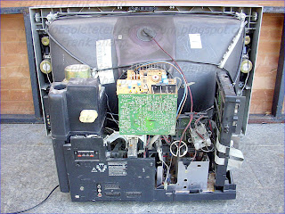 ersion method of generating an output video signal from an interlaced input signal, including the steps of furnishing (1) a first signal having first lines (Fi (x-(0, 1)T, n)) corresponding to original lines of the interlaced input signal, and second lines (Fi (x, n)) in addition to the first lines (Fi (x-(0, 1)T, n)); and providing (5, 11, 7, 13) a second signal which is delayed or advanced with respect to the first signal, the second signal having first processed lines (Fout (x-(0, 1)T -D, n-1)) corresponding to the original lines, and second processed lines (Fout (x-D, n-1)) corres
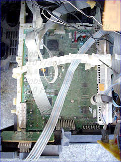 ponding to the second lines (Fi (x, n)); output lines (Fout (x, n)) of the output video signal are obtained in dependence upon a first difference between the first processed lines (Fout (x-(0, 1)T -D, n-1)) and the first lines (Fi (x-(0, 1)T, n)), and a second difference between the second processed lines (Fout (x-D, n-1)) and the second lines (Fi (x, n)).
1. A scan conversion method of generating an output video signal from an interlaced input signal, comprising the steps of:
furnishing a first signal having first lines (Fi (x-(0, 1)T, n)) corresponding to original lines of said interlaced input signal, and second separate lines (Fi (x, n)) in addition to said first lines (Fi (x-(0, 1)T, n)); and
providing a second signal which is delayed or advanced with respect to said first signal, said second signal having first processed lines (Fout (x-(0, 1)T -D, n-1)) corresponding to said original lines, and second processed lines (Fout (x-D, n-1)) corresponding to said second lines (Fi (x, n));
characterized in that output lines (Fout (x, n)) of said output video signal are obtained in dependence upon
a first mixer-generated difference between said first processed lines (Fout (x-(0, 1)T -D, n-1)) and said first lines (Fi (x-(0, 1)T, n)), and
a second mixer-generated difference between said second processed lines (Fout (x-D, n-1)) and said second lines (Fi (x, n)).
2. A method as claimed in claim 1, wherein said output video signal is a sequentially scanned video signal, and wherein the method comprises the further step of combining said first signal and said second signal to obtain an output sequentially scanned video signal having first output lines (Fout (x-(0, 1)T, n)) corresponding to said original lines, and said output lines (Fout (x, n)) between said first output lines (Fout (x-(0, 1)T, n)).
3. A method as claimed in claim 2, wherein said output lines (Fout (x, n)) of said output video signal are obtained further in dependence upon a relation (k2) between said first lines (Fi (x-(0, 1)T, n)) and said first output lines (Fout (x-(0, 1)T, n)).
4. A method as claimed in claim 1, wherein said first processed lines (Fout (x-(0, 1)T -D, n-1)) and said second processed lines (Fout (x-D, n-1)) are obtained by means of a motion-compensated interpolation.
5. A method as claimed in claim 2, wherein said output lines are obtained in dependence upon said second difference and a third difference between said first output lines (Fout (x-(0, 1)T, n)) and said first processed lines (Fout (x-(0, 1)T -D, n-1)).
6. A method as claimed in claim 2, wherein said combining step is controlled such that a difference between said output lines (Fout (x, n)) and said second processed lines (Fout (x-D, n-1)) corresponds to a difference between said first output lines (Fout (x-(0, 1)T, n)) and said first processed lines (Fout (x-(0, 1)T -D, n-1)).
7. A method as claimed in claim 1, wherein said first and second differences are absolute differences.
8. A scan conversion apparatus for generating an output video signal from an interlaced input signal, comprising:
means for furnishing a first signal having first lines (Fi (x-(0, 1)T, n)) corresponding to original lines of said interlaced input signal, and separate second lines (Fi (x, n)) in addition to said first lines (Fi (x-(0, 1)T, n)); and
means for providing a second signal which is delayed or advanced with respect to said first signal, said second signal having first processed lines (Fout (x-(0, 1)T -D, n-1)) corresponding to said original lines, and second processed lines (Fout (x-D, n-1)) corresponding to said second lines (Fi (x, n));
characterized in that said scan conversion apparatus further comprises means for generating output lines (Fout (x, n)) of said output video signal in dependence upon
a first mixer-generated difference between said first processed lines (Fout (x-(0, 1)T -D, n-1)) and said first lines (Fi (x-(0, 1)T, n)), and
a second mixer-generated difference between said second processed lines (Fout (x-D, n-1)) and said second lines (Fi (x, n)).
9. An apparatus as claimed in claim 8, wherein said output video signal is a sequentially scanned video signal, and wherein the apparatus further comprises means for combining said first signal and said second signal to obtain an output sequentially scanned video signal having first output lines (Fout (x-(0, 1)T, n)) corresponding to said original lines, and said output lines (Fout (x, n)) between said first output lines (Fout (x-(0, 1)T, n)).
10. An apparatus as claimed in claim 9, wherein said output lines (Fout (x, n)) of said output video signal are obtained further in dependence upon a relation (k2) between said first lines (Fi (x-(0, 1)T, n)) and said first output lines (Fout (x-(0, 1)T, n)).
11. An apparatus as claimed in claim 9, wherein said output lines are obtained in dependence upon said second difference and a third difference between said first output lines (Fout (x-(0, 1)T, n)) and said first processed lines (Fout (x-(0, 1)T -D, n-1)).
12. An apparatus as claimed in claim 9, wherein said combining means are controlled such that a difference between said output lines (Fout (x, n)) and said second processed lines (Fout (x-D, n-1)) corresponds to a difference between said first output lines (Fout (x-(0, 1)T, n)) and said first processed lines (Fout (x-(0, 1)T -D, n-1)).
13. A video signal display apparatus comprising:
means for supplying an interlaced input signal;
a scan conversion apparatus for generating an output video signal from said interlaced input signal, as claimed in claim 8; and
means for displaying (16) said output video signal.
BACKGROUND OF THE INVENTION
1. Field of the Invention
The invention relates to a method and apparatus for video signal scan conversion, and to a video signal display apparatus comprising such a conversion apparatus.
2. Description of the Related Art
WO-A-95/27362, corresponding to U.S. Pat. No. 5,532,750 (Attorney's reference PHN 14,794), discloses a method of converting an interlaced video signal into an output sequentially scanned video signal. A first sequentially scanned video signal is furnished in dependence upon the interlaced video signal. Subsequently, a motion-compensated sequentially scanned signal is furnished in dependence upon the first sequentially scanned video signal. All video lines of the output sequentially scanned video signal are generated in dependence upon both the first sequentially scanned video signal and the motion-compensated sequentially scanned signal to prevent inaccuracies in motion vectors used in the motion-compensated processing operation from resulting in visible distortions. The first sequentially scanned video signal and the motion-compensated sequentially scanned signal are combined to furnish the output sequentially scanned video signal by means of a first mixer for first lines positionally corresponding to original lines of a present field of the interlaced video signal, a second mixer for second lines positionally corresponding to interpolated lines between the original lines, and a multiplexer for line-alternately selecting an output of the first mixer or an output of the second mixer.
SUMMARY OF THE INVENTION
It is, inter alia, an object of the invention to provide an improved video signal scan conversion.
Accordingly, a first aspect of the invention provides a method of generating an output video signal from an interlaced input signal, comprising the steps of:
furnishing a first signal having first lines (F i (x-(0, 1) T , n)) corresponding to original lines of the interlaced input signal, and second lines (F i (x, n)) in addition to the first lines (F i (x-(0, 1) T , n)); and
providing a second signal which is delayed or advanced with respect to the first signal, the second signal having first processed lines (F out (x-(0, 1) T -D, n-1)) corresponding to the original lines, and second processed lines (F out (x-D, n-1)) corresponding to the second lines (F i (x, n));
in which output lines (F out (x, n)) of the output video signal are obtained in dependence upon
a first difference between the first processed lines (F out (x-(0, 1) T -D, n-1)) and the first lines (F i (x-(0, 1) T , n)), and
a second difference between the second processed lines (F out (x-D, n-1)) and the second lines (F i (x, n)).
Preferably, the output video signal is a sequentially scanned video signal, and the method comprises the further step of combining the first signal and said second signal to obtain the output sequentially scanned video signal having first output lines (F out (x-(0, 1) T , n)) corresponding to the original lines, and the output lines (F out (x, n)) between the first output lines (F out (x-(0, 1) T , n)). Advantageously, the output lines (F out (x, n)) of the output video signal are obtained further in dependence upon a relation between the first lines (F i (x-(0, 1) T , n)) and the first output lines (F out (x-(0, 1) T , n)).
A refinement of the first aspect of the invention provides that the output lines are obtained in dependence upon the second difference and a third difference between the first output lines (F out (x-(0, 1) T , n)) and the first processed lines (F out (x-(0, 1) T -D, n-1)), in which the first difference as well as the relation between the first lines and the first output lines are replaced by a third difference which is equivalent thereto in a preferred embodiment of the invention.
Another refinement of the first aspect of the invention provides that the combining step is controlled such that a difference between the output lines (F out (x, n)) and the second processed lines (F out (x-D, n-1)) corresponds to a difference between the first output lines (F out (x-(0, 1) T , n)) and the first processed lines (F out (x-(0, 1) T -D, n-1)). The above-mentioned aspects of the invention improve the consistency along the motion trajectory or, put in other words, a smoother picture is obtained for moving objects.
A second aspect of the invention provides a scan conversion apparatus for generating an output video signal from an interlaced input signal, comprising means for furnishing a first signal having first lines (F i (x-(0, 1) T , n)) corresponding to original lines of said interlaced input signal, and second lines (F i (x, n)) in addition to said first lines (F i (x-(0, 1) T , n)); and means for providing a second signal which is delayed or advanced with respect to said first signal, said second signal having first processed lines (F out (x-(0, 1) T -D, n-1)) corresponding to said original lines, and second processed lines (F out (x-D, n-1)) corresponding to said second lines (F i (x, n)); characterized in that said apparatus further comprises means for generating output lines (F out (x, n)) of said output video signal in dependence upon a first difference between said first processed lines (F out (x-(0, 1) T -D, n-1)) and said first lines (F i (x-(0, 1) T , n)), and a second difference between said second processed lines (F out (x-D, n-1)) and said second lines (F i (x, n)).
A third aspect of the invention provides a video signal display apparatus incorporating such a scan conversion apparatus as described.
BRIEF DESCRIPTION OF THE DRAWINGS
In the drawings:
FIG.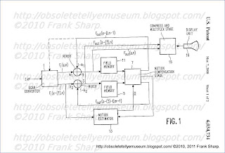 1 illustrates an embodiment of a television receiver comprising a sequential scan converter in accordance with the present invention;
FIG. 2 shows an embodiment of a device for calculating mixer coefficients k1 and k2 for use in the embodiment of FIG. 1; and
FIG. 3 shows an embodiment of a device for calculating the mixer coefficient k1 for use in the embodiment of FIG. 1.
DESCRIPTION OF THE PREFERRED EMBODIMENTS
1. Introduction
De-interlacing i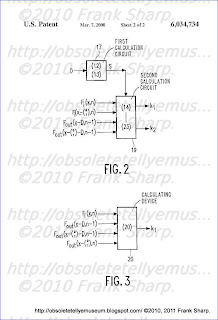 s a basic operation required for most video scanning format conversions. Vertical and temporal interpolation of image data cause practical and fundamental difficulties, as the conditions of the sampling theorem are generally not met in video signals. Linear methods, based on sampling rate conversion theory, therefore negatively influence the resolution and/or the motion portrayal. The more advanced algorithms can be characterized by their common attempt to interpolate the 3-D image data in the direction with the highest correlation. To this end, they either have an explicit or implicit detector to find this direction. In case of 1-D temporal interpolation the explicit detector is usually called a motion detector, for 2-D spatial interpolation it is called an edge detector, while the most advanced device estimating the optimal spatio-temporal 3-D interpolation direction is a motion estimator. The interpolation filter can either be recursive or transversal, but the number of taps in the temporal direction is preferably small.
Recently, some papers have been published proposing a recursive scheme for motion compensated sequential scan conversion (References [1] and [2]). Experiments indicate that the recursiveness yields a significant improvement of the motion-compensated median (Reference [3]), on which these algorithms are based, if good quality motion vectors are available. Furthermore, recursiveness is expected to allow an improved performance on critical velocities, compared to recently published methods applying generalized sampling theory (Reference [4]), if the velocities are accelerating. In this application an improved recursive sequential scan conversion algorithm is introduced that suppresses remaining artifacts of the prior art further. The invention provides the algorithms and a novel evaluation method that shows the improvement in an objective score. For high quality, sub-pixel accurate motion estimation the algorithm of (Reference [5]) is used.
2. De-interlacing techniques
In general, the samples required for the motion compensated de-interlacing do not exist in the time discrete input signal, e.g. due to non-integer velocities. In the horizontal domain this problem can be solved with linear Sampling Rate Conversion (SRC) theory, e.g. (Reference [6]), but not in the vertical domain, as the constraints of the sampling theorem are not met. Three different solutions for this problem have been proposed recently in the literature:
(1) A straight extension of the motion vector into earlier pictures until it points (almost) to an existing pixel (Reference [7]).
(2) The application of a generalized sampling theory (GST) (Reference [4]).
(3) Recursive de-interlacing of the signal (Reference [1] and [2]).
Solution (1) is valid only if we assume the velocity constant over a larger temporal instance. This is a rather severe limitation which makes the method practically useless.
The implication of GST is that it is possible to perfectly reconstruct a signal sampled at 1/n times the Nyquist rate with n independent sets of samples that describe the signal. For the de-interlacing problem n=2, and the required two sets are the current field and the motion compensated previous field. If the two do not coincide, i.e., the object does not have an odd vertical motion vector component, the independency constraint is fulfilled, and the problem can theoretically be solved. Practical problems are:
a) The velocity can have an odd vertical component.
b) A perfect reconstruction requires the use of pixels from many lines, for which the velocity needs not be constant.
c) For velocities near the vertical odds, noise may be enhanced.
Solution (3) is based on the assumption that it is possible at some time to have a perfectly de-interlaced picture in a memory. Once this is true, the picture is used to de-interlace the next input field. With motion compensation, this solution can be perfect as the de-interlaced picture in the memory allows the use of SRC-theory also in the vertical domain. If this new de-interlaced field is written in the memory, it can be used to de-interlace the next incoming field etc. Limitations of this method are:
(I) Propagation of errors due to motion vector inaccuracy and interpolation defects
(II) Even a perfectly de-interlaced picture can contain alias in the vertical frequency domain, assuming the common case of a camera without optical pre-filter.
In practice problem (I) is the more serious, particularly for nearly odd vertical velocities and/or noisy input signals.
We concluded that recursive de-interlacing and de-interlacing based on GST are the best methods presently known. However, even these best methods are imperfect. It is our target to present an improvement that can be applied in combination with both methods to suppress the remaining artifacts in the de-interlaced output signal. In fact, our proposal can be used to improve any de-interlacing algorithm.
3. Description of the Applied Algorithms
In Reference [1] a time-recursive de-interlacing algorithm is proposed in which the lines that need to be interpolated are found by motion compensating the previously found de-interlaced output frame: ##EQU1## where F(x, t) is the interlaced input signal, F out (x, n) the sequential output, n the field number, and x is the spatial position.
To prevent errors from propagating, in Reference [1] several additional measures are described to protect the interpolated lines. Particularly, the median filter is proposed to realize this protection:
Although further alternatives are suggested in Reference [1], we will use this algorithm as the basis for our comparison. ##EQU2##
As we expect the quality of Reference the resulting algorithm to depend heavily on the performance of the motion estimator, we applied the motion estimation method of [5]. This high quality algorithm yields a quarter pixel accuracy, and a close to true-motion vector field which is considered very important for scan rate conversion. Rather than calculating all possible candidate vectors, this recursive search block-matcher takes spatial and/or temporal "prediction vectors" from a 3-D neighborhood, and a single updated prediction vector. This implicitly assumes spatial and/or temporal consistency. The updating process involves update vectors added to either of the spatial prediction vectors. We applied a candidate set CS(X, n), from which the block-matcher selects its result vector, defined by: ##EQU3## where the update vectors U a (X, n) and U b (X, n) are alternatingly (on block basis) available, and are taken from a limited fixed integer update set, in our case: ##EQU4## To realize sub-pixel accuracy, the update set of equation (4) is extended with fractional update values. We realized a quarter pixel resolution by adding the following fractional update vectors to the update set: ##EQU5## Because of the small number of candidate vectors, the method is very efficient and realizes, due to the inherent smoothness constraint, very coherent and close to true-motion vector fields, most suitable for scanning format conversion.
4. Recursive de-interlacing algorithm
The main imperfection of the recursive de-interlacing algorithm is remaining alias in the output signal. Although this imperfection is usually worse for alternative methods, further improvement seems attractive. Difficulty with this defect is that it is hardly visible in single images but mainly in moving sequences. This makes it difficult to illustrate, while also quantitative measures to show the improvement seem to lack.
A common method for evaluating the de-interlacing quality is comparing an original sequentially scanned image with a de-interlaced result using a, what we will call here, MSEs-criterion: ##EQU6##
This criterion is not exclusively sensitive for remaining alias, as it sums all differences without discriminating for different backgrounds, e.g., due to resolution losses, noise, vector errors, etc. An additional inconvenience of this criterion is that it cannot be applied to check the performance of the algorithm on original interlaced source signals.
In a perfectly de-interlaced picture (without residual alias), a characteristic is that the sequence is stationary along the motion trajectory, in picture parts for which the motion model is valid. Based upon this characteristic, an alternative was suggested in where we measured how well the current interlaced input field n was predicted by the motion compensated previously de-interlaced field: ##EQU7## This method has the advantage that it can be applied to judge the performance in absence of an original sequentially scanned sequence. However, the measure has limited value in case of critical velocities, as in that case the quality of the interpolated lines is not reflected in the figure.
In an attempt to improve on this aspect, it is possible to measure a "Motion Trajectory Inconsistency" (MTI(n)) for all output lines in field n, which we will define as: ##EQU8## A problem with this measure is that a good score on this criterion is a necessary but not sufficient constraint in the processing. It is possible, e.g. applying a strong temporal filtering, to force this MTI to very low values, while obviously the picture quality is degraded. However, a lower score on the MTI criterion coupled to a hardly varying MSE score is a strong indication for quality improvement. There is a clear analogy with the motion vector smoothness constraint (see Reference [8]), where motion estimation techniques have been improved by adding a smoothness term in the match criterion which yields a significant consistency improvement accepting a slight MSE degradation. Quite similarly, it is possible here to introduce a de-interlacing cost figure defmed as: ##EQU9## The parameter α allows tuning of the cost function to match the subjective impression.
After quantifying "remaining alias" applying equation (9), an improvement of the MTI figure could be realized by suppressing non-stationarities along the motion trajectory. As long as this does not seriously degrades the MSE-score, it brings an improved Cost-score and, with α tuned correctly, also an improved subjective performance.
As non-stationarities can reside on interpolated lines as well as on original lines, the implication would be that both have to be temporally filtered. That filtering of original lines, which is somewhat contra-intuitive, helps to suppress remaining alias can also be understood from the vertical frequency spectrum of the signal on original and interpolated lines respectively. In the original recursive de-interlacing algorithm, the lines existing in the input field are always directly transferred to the output and never modified. As the first repeat spectrum of the interpolated lines will almost always suffer from inaccuracies in the motion vector estimates and the protection features, this spectrum cannot fully compensate for the (anti-phase) repeat spectrum resulting from the original lines.
As a consequence of the above, the recursive de-interlacing method that we propose interpolates not only the new lines, but, in an attempt to maximize the motion trajectory consistency on both type of lines equally strong, also the lines existing in the interlaced signal: F out (x, n)=k(R).(F out (x-D(x, n), n-1)+(1-k(R)).(F i (x, n))(10)
where k(R) is a control parameter that reflects the reliability R of the motion vectors. F i (x, n) can be calculated according to equation (2) but also, with little disadvantage as we will show later, using a simpler intra-field interpolation: ##EQU10## In the literature, sometimes the match error, or the match error corrected for the local picture contrast is used. When applying the 3-D Recursive Search block-matcher described in Reference [5], another indication for motion vector reliability is available. This recursive estimator, due to the use of spatial and temporal predictions, implicitly assumes consistent motion vector fields. If the output vector field is not smooth than the implicit assumption may be false, and therefore the motion vectors unreliable.
For this smoothness, any sum of absolute (or squared) differences of the current vector with its spatial and temporal neighbors can be applied, but using the 3-D RS block-matcher, we obtained good results using the following definition for the vector smoothness S: ##EQU11## where p=(x, y, t) T is the spatio-temporal position, α is a constant selected experimentally, while the neighborhood N in which the neighboring vectors are found defined as: ##EQU12## In this definition X and Y denote the horizontal and vertical block dimensions as used in the motion estimator respectively.
5. Refinements of the Algorithm
The severest drawbacks that were found with the above-described algorithm were:
(1) Large homogeneously moving picture parts occasionally break up into several areas with slightly different velocities (earthquakes).
(2) In areas where large displacement discontinuities occurred, blocking artifacts were sometimes visible. These are due to the reliability indicator being available on block base only.
The first of these difficulties is directly related to the fundament of the proposed method and, therefore, most difficult to cure: by recursively filtering both the original and the interpolated lines, the output becomes more and more "isolated from the input" if the reliability of the motion vectors is considered to be good. In this section, therefore, we introduce a solution to prevent the output pictures from drifting too far from the input material.
The basis for the refinement is to detect directly how far the filtered information on an original line differs from the unfiltered information and to reduce the filtering in case the deviation becomes to large. As this adaptation of the filtering can easily be realized on a pixel base, it further provides a means to cope with the drawback mentioned under number (2). The same difference is used to reduce the filtering of the interpolated lines, albeit that much larger differences turned out to be tolerable.
In the refined algorithm (modification of equation (2) the output luminance is found as: ##EQU13## and using a limiter function "clip" defined as: ##EQU14## k 2 is calculated as: ##EQU15## Consequently, k 2 is a function of the vector smoothness S, defined in equation (4), and of the (pixel-) difference, Diff, in the motion compensated recursive loop measured on original lines of the interlaced grid only: ##EQU16## where W is a window containing the six pixels nearest to the currently interpolated pixel on the lines directly above and below the interpolated pixel. As Diff is related to the MSE i (n) of equation (7), it is possible by appropriately choosing C 1 , to tune the relative importance of MSE i (n) and MTI(n).
Although this tuning seems rather straightforward for the original lines, it is more complicated for the interpolated lines. For these lines, an MTI(n) figure can be calculated, but a significant MSE i (n) cannot be found, as the quality of the input lines to this temporal filter depends on the quality of the initial sequential scan conversion algorithm. To escape from this fundamental problem, we propose here to tune k 1 such that the contribution of original lines and interpolated lines to the MTI(n) figure is identical per pixel, disregarding the energy over the temporal filter for the interpolated lines. The assumption leads to: ##EQU17## while at the same time: F out (x, n)=k 1 F i (x, n)+(1-k 1 )F out (x-D, n-1)(19)
where F i (x, n) is the output of the initial de-interlacing algorithm, e.g., using equation (2) or (11). Combination of equations (18) and (19), results in a calculation of k 1 according to: ##EQU18## Combining this result with the lower part of equation (14) results in: ##EQU19## As an implication, the temporal recursive filtering on the interpolated lines depends on the quality of the initial de-interlacing method. A simple line averaging algorithm will cause stronger temporal filtering, of the interpolated lines, than e.g. a motion compensated median filter. Experimentally, we could show that the difference in resulting de-interlacing performance was small.
The assumption of equation (18) leads to an adaptation of temporal recursive filtering on the interpolated line applying differences measured on the upper neighboring original line. Rather than using the upper original line as a reference, the lower neighboring line can be used equally well. For symmetry considerations, the average effect on the two neighboring original lines seems advantageous. Elaborating this results in a symmetrical alternative for equation (20): ##EQU20## with: ##EQU21##
Rather than averaging the absolute differences, it is possible to take the absolute value of the average, the maximum of the two averages, or apply (2-D) spatial filters before and/or after the rectifier (abs). The choices resemble those commonly applied in motion detectors. It is furthermore possible to apply the above control of the temporal filter on the interpolated lines, while fixing the value of k 2 to no filtering on the original lines (k 2 =1). Generally, this will lead to somewhat lower MSE i (n) figures, but a significantly higher MTI(n) score.
In an alternative embodiment, k 2 is calculated as: ##EQU22## with: Diff(x, n)=abs(F out (x-D(x, n), n-1)-(F i (x, n)) (25)
Consequently, k 2 is a function of the prediction error, Diff, in the motion compensated recursive loop. As Diff is related to the MSE(n) of equation (7), it is possible by appropriately choosing C 2 , to tune the relative importance of MSE i (n) and MTI(n).
As the quality of the interpolated pixels, as resulting from the initial de-interlacing method, is obviously less than that of the original pixels, the filtering of these pixels should be stronger. As, furthermore, Diff(x, n), at the position of the interpolated lines, has little value to determine the quality of the motion compensated prediction, we propose to control k 1 using: ##EQU23## where C 1 is smaller than C 2 , and the control of the recursive filter for interpolated pixels is derived from the quality of the motion compensated prediction at the vertically neighboring existing pixels.
There is a risk in filtering alternate lines differently, as it potentially introduces visible line structures. Although the advantage of high quality de-interlacing will be apparent in areas with vertical detail, there is no advantage in regions that lack such high vertical frequency components. Therefore, in order to prevent the introduction of line structure in image parts that never profit from individual filtering, k 1 is made equal to k 2 if: ##EQU24##
To evaluate the proposals resulting from the previous section, we selected a set of 4 critical sequences. The sequences contain vertical detail, and motion with various sub-pixel values in many directions. Using the algorithm of Reference [1], in the version described in section 2 as a above reference, we calculated MSEs and MTIs for another two algorithms, illustrating the proposals of this paper. The first algorithm is the one illustrated in FIG. 1, in which the control of the recursive loop is according to equations (24,26). The second algorithm has k 2 fixed at 1, i.e., no recursive filtering of the original pixels, and is further identical. Compared to the reference algorithm, both proposed new algorithms yield a slightly improved MSE i figure, which is expected to be mainly due to the elimination of median defects in the high spatial frequencies. The MTI figures, however, have been improved dramatically, particularly for the first algorithm, i.e., the algorithm that performs recursive filtering even on the original lines. MSE i figures of both algorithm differ only little. The additional recursive filtering of the original pixels mainly improves the MTI figure (with little or no disadvantage for the MSE i figure).
FIG. 1 shows the resulting architecture of the proposed de-interlacing algorithm. In FIG. 1, an interlaced input signal is applied from an input I to an initial sequential scan converter 1 which supplies original lines at its lower output and interpolated lines at its upper output. The original lines are applied to a motion compensation stage 7 thru a mixer 3 and a field memory 5. Similarly, the interpolated lines are applied to the motion compensation stage 7 thru a mixer 9 and a field memory 11. Motion vectors D for the motion compensation stage 7 are determined by a motion estimator 13 on the basis of the original lines supplied by the initial sequential scan converter 1 (or on the basis of the lines supplied by the mixer 3), and shifted lines supplied by the motion compensation stage 7. Motion compensated shifted lines are supplied by the motion compensation stage 7 to the mixers 3 and 9. The mixer 3 mixes the original lines and the motion compensated shifted lines in the ratio k2: (1-k2). The mixer 9 mixes the interpolated lines from the initial sequential scan converter 1 and the motion compensated shifted lines in the ratio k1:(1-k1). Output signals from the mixers 3 and 9 are applied to a compress and multiplex stage 15 to generate a de-interlaced output signal, which is displayed on a display unit 16.
While this embodiment largely corresponds to that described in WO-A-95/27362 (Attorney's reference PHN 14,794), the present invention is mainly concerned with providing optimal values for k1 (and k2). To this end, FIG. 2 shows an embodiment of a device for calculating the mixer coefficients k1 and k2 for use in the embodiment of FIG. 1. The mixer coefficients calculating device of FIG. 2 contains a first calculation circuit 17 for calculating a vector smoothness S in response to the motion vectors D in accordance with equations 12, 13, and a second calculation circuit 19 for calculating the mixing factors k1 and k2 in dependence upon the four signals applied to the mixers 3 and 9 in accordance with equations 14 thru 23.
FIG. 3 shows an embodiment of a device for calculating the mixer coefficient k1 for use in the embodiment of FIG. 1. The mixer coefficient k2 has a fixed value of 1. The mixer coefficient k1 is calculated in accordance with equation 20 by a calculating device 20.
6. Conclusion
A generally applicable improvement to existing de-interlacing algorithms and a new evaluation measure for such algorithms have been proposed in this application. A motion-compensated temporal recursive filtering is used. A typical feature of the proposal is that this filtering is not limited to the interpolated pixels only, but is extended to the filtering of the pixels existing in the interlaced input signal. This somewhat contra-intuitive action followed from the assumption that in order to have the repeat spectra of original lines compensated by that of the interpolated ones, it is essential that the two have identical frequency response. As it cannot be prevented that of the interpolated pixels may be distorted by the limited accuracy of the applied motion vectors, a similar distortion can best be applied to that of the original pixels in order to maximally suppress alias. The application of the improvement to time-recursive de-interlacing was elaborated and the improved performance was verified. The verification has to be understood in a sense that the classical MSE i performance measure had not suffered (in fact, even showed some improvement), whereas the new proposed "consistency along the motion trajectory" (MTI) had greatly improved.
In a preferred embodiment, the invention provides a method of sequential scan conversion which uses a recursive temporal filtering of at least the interpolated lines, in which the filter is controlled by locally giving a resulting consistency along the motion trajectory a fixed relation (e.g. 1), to the values determined for adjacent lines.
It should be noted that the above-mentioned embodiments illustrate rather than limit the invention, and that those skilled in the art will be able to design many alternative embodiments without departing from the scope of the appended claims. While absolute differences are described, in some embodiments, normal differences are used to preserve the sign of the difference. FIG. 1 shows a recursive embodiment, in which the outputs of the mixers 3, 9 are applied to the motion-compensation stage 7 thru the field memories 5, 11; of course, a non-recursive embodiment in which the inputs of the field memories 5, 11 are directly connected to the outputs of the initial sequential scan convertor 1 is also possible. In FIG. 1, the interpolated lines supplied by the initial sequential scan convertor 1 may be just white, black or grey lines; if an interpolation algorithm is used to obtain the interpolated lines, any algorithm will do. In the claims, any reference signs placed between parentheses shall not be construed as limiting the claim. The invention can be implemented by means of hardware comprising several distinct elements, and by means of a suitably programmed computer.
Accordingly, a preferred embodiment of the invention provides a method of generating a sequentially scanned video signal from an interlaced input signal, comprising the steps of: furnishing a first signal having first lines (F i (x-(0, 1) T , n)) corresponding to original lines of the interlaced input signal, and second lines (F i (x, n)) in addition to the first lines (F i (x-(0, 1) T , n)); and
providing a second signal having first motion-compensated lines (F out (x-(0, 1) T -D, n-1)) corresponding to the original lines, and second motion-compensated lines (F out (x-D, n-1)) corresponding to the second lines (F i (x, n));
combining the first signal and the motion-compensated signal to obtain an output sequentially scanned video signal having first output lines (F out (x-(0, 1) T , n)) corresponding to the original lines, and second output lines (F out (x, n)) between the first output lines (F out (x-(0, 1) T , n));
wherein the second output lines (F out (x, n)) are obtained in dependence upon (see equations 21 and 27):
a first difference between the first motion-compensated lines (F out (x-(0, 1) T -D, n-1)) and the first lines (F i (x-(0, 1) T , n)),
a second difference between the second motion-compensated lines (F out (x-D, n-1)) and the second lines (F i (x, n)), and
a relation (k 2 ) between the first lines (F i (x-(0, 1) T , n)) and the first output lines (F out (x-(0, 1) T , n)).
However, it is not necessary that the output video signal is a sequentially scanned video signal, as the invention can advantageously be used to derive an output interlaced signal having its output lines vertically positioned between the lines of the input interlaced signal. Such an interlaced-to-interlaced conversion is needed in 100 Hz conversion, where the lines one of the input interlaced fields need to be vertically shifted towards the positions of the lines of the other input interlaced field. The combining step is advantageous in a sequential scan conversion, but not necessary in other scan conversions.
Also, while the second signal is preferably obtained by means of a motion-compensated interpolation, satisfactory results can already be obtained when a less complex method is used to obtain a second signal which is delayed or advanced with respect to the first signal, like one which uses a median filter.
Finally, the dependence on the relation (k 2 ) between the first lines and the first output lines appeared to contribute to an improved result, while good results were already obtained when the output lines were dependent only on the first and second differences.
The invention can advantageously be applied in a video signal display apparatus like a television receiver or a personal computer.
7. References
[1] F. M. Wang, D. Anastassiou, and A. N. Netravali, `Time-Recursive Deinterlacing for IDTV and Pyramid Coding`, Signal processing: Image Communication 2, Elsevier 1990, pp. 365-374.
[2] Kwon, Seo, Kim, and Kim, `A Motion Adaptive De-Interlacing Method`, IEEE Transactions on Consumer Electronics, Vol. 38, No.3, 1992.
[3] G. de Haan and G. F. M. De Poortere, `Method and apparatus for processing a picture signal`, EP-A-0,474,287.
[4] P. Delogne, L. Cuverlier, B. Maison, B. Van Caillie, and L. Vandendorpe, "Improved Interpolation, Motion Estimation, and Compensation for Interlaced Pictures", IEEE Transactions on Image Processing, Vol. 3, No. 5, September 1994.
[5] G. de Haan, and P. W. A. C. Biezen, `Sub-pixel motion estimation with 3-D recursive search block-matching`, Signal Processing: Image Communication 6 (1994), pp. 229-239.
[6] A. W. M. van den Enden and N. A. M. Verhoeckx, Discrete-time signal processing, Prentice Hall (ISBN 0-13-216763-8), pp. 233-.
[7] J. W. Woods and S. C. Han, "Hierarchical Motion Compensated De-interlacing", Proc. SPIE Visual Communication and Image Processing VI, Boston, November 1991.
[8] G. de Haan, P. W. A. C Biezen, H. Huijgen, and O. A. Ojo, "True Motion Estimation with 3-D Recursive Search Block-Matching", IEEE Transactions on Circuits & Systems for Video Technology, Vol. 3, October 1993, pp. 368-388.
REFERENCES LIST:
A. Semiconductor Devices and Physics
1. J. Baliga and D. Y. Chen (Eds.), Power Transistors: Device Design and Applications, IEEE
Press, New York, 1984.
2. J. Biliga, Modern Power Devices, John Wiley, New York, 1987.
3. Blicher, Thyristor Physics, Springer-Verlag New York Inc.,1976.
4. K. Ghandhi, Semiconductor Power Devices Physics of Operation and Fabrication Technology,
John Wiley & Sons, Inc.,New York, 1977.
5. G. Hoft, Semiconductor Power Electronics, Van Nostrand Reinhold Company Inc.,1986.
(ISBN: 0-442-22543-1)
6. P .
L. Hower, Power semiconductor devices: an overview, IEEE Proc., Wvol. 76, no. 4, pp.
335-342, April 1988.
7. C. Lee and D. Y. Chen (Ed.), Power Devices and Their Applications, Virginia Power
Electronics Center, 1990.
8. Ohmi, Power static induction transistor technology," Technical Digest, IEEE Electron Devices
International Meeting, Washington, D.C., pp. 84-87, 1979.
9. Shockley, A unipolar field-effect transistor ,"
Proc. IRE, vol. 40, pp. 1365-1376, Nov. 1952.
10. Shockley, How we invented the transistor," New Scientist, vol. 689, Dec. 21, 1972.
11. Shockley, The path to the conception of the junction transistor," IEEE Trans. Electron Devices
23, vol. 597, 1976.
12. G. Streetman, Solid State Electronic Devices, Prentice-Hall, Inc., 1980.
13. M. SZE, Semiconductor Devices: Physics and Technology, Bell Telephone Lab., Inc., 1985.
14. Teszner and R. Giqual, Gridistor - a new field-effect device," Proc. IEEE, vol. 52, pp. 1502-
1513, 1964.
15. M. Warner and B. L. Grung, Transistors: Fundamentals for the Integrated-Circuit Engineer
,
1983.
16. Wood, Fundamentals and Applications of Gate Turn-off Thyristors, Electric Power Research
Institute, Palo Alto, 1988.
17. S. Yang, Fundamental of Semiconductor Devices, McGraw-Hill Book Company, 1978.
18. Zuleeg, Multi-Channel field-effect transistor, theory and experiment," Solid-State Electronics,
vol. 10, pp. 559-576, 1967.
B. Power Electronics
19. D. Bedford and R. G. Hoft, Principles of Inverter Circuits, 1985 Reprint Edition, Robert E.
Krieger Publishing Company, Malabar, Florida, 1964.
20. M. Bird and K. G. King, An Introduction to Power Electronics,1983. (ISBN: 0-471-10430-
2)
21. B. K. Bose, Adjustable Speed A C Drive Systems, IEEE Press, New York, 1982.
22. B. K. Bose, "Power electronics - an emerging technology", IEEE Trans. on Ind. Electron., vol.
36, no. 3, pp. 404-412, Aug. 1989.
23. B. K. Bose, Microcomputer Control of Power Electronics and Drives, IEEE Press, New
York, 1987.
24. B. K. Bose., Modern Power Electronics, Evolution, Technology and Applications, IEEE
Press, New York, 1991.
25. B. K. Bose,"Power electronics - an emerging technology," IEEE Trans. on Ind. Electron., vol.
36, no. 3, pp. 403-412, 1989.
26. B. K. Bose, Power Electronics and A C Drives, Prentice Hall, Englewood Cliffs, 1986.
27. B. K. Bose, Power Electronics and A C Drives, Prentice-Hall, New Jersey, 1987.
(TK7881.15.B67).
28. B. K. Bose, "Power electronics and motion control technology," IEEE, pp. 1-10, 1992.
29. B. K. Bose, "Technology trends in microcomputer control of electrical machines," IEEE
Trans. on Ind. Electron., vol. 35, no. 1, pp. 160-177, Feb. 1988.
30. A. Coekin, High-Speed Pulse Techniques, Pergamon, 1975. (TK7835.C56 1975).
31. Csaki, I. Hermann, I. Ipsits, A. Karpati, and P .
Magyar, Power Electronics Akademiai Kiado,
Budapest, 1979. (ISBN 963-05-1671-3).
32. B. Dewan and A. Straughen, Power Semiconductor Circuits, John Wiley & Sons, Inc., 1975.
33. K. Dubey, Power Semiconductor Controlled Drives, Prentice Hall, Englewood Cliffs, 1985.
34. Hans-Peter Hempel, Power Semiconductor Handbook, SEMIKRON, 1980. (ISBN 3-
9800346-1-5).
35. R. G. Hoft, Semiconductor Power Electronics, Van Nostrand, New York, 1986.
(TK7871.85.H65).
36. L. Kusic, Computer-Aided Power Systems Analysis, Prentice-Hall, 1986. (TK1005.K87
1986).
37. W. Lander ,
Power Electronics, McGraw-Hill, 1981. (ISBN: 0-07-084123-3).
38. M. Miller, Is power electronics a national priority ?, Power Conversion & Intelligent
Motion Control, March 1987.
39. Mohan, T. M. Undeeland, and P .
Robbins, Power Electronics, John Wiley, New York, 1989.
40. M. D. Murphy and F. G. Turnbull, Power Electronic Control of A C Motors, Pergamon, New
York, 1988.
41. E. Newell and J. W. Motto, Introduction to Solid State Power Electronics, Youngwood:
Westinghouse Electric Corporation, 1977.
42. S. Oxner, Power FETs and Their Applications, Prentice-Hall Inc., 1982.
43. Pearman, Power Electronics: Solid State Motor Control, Reston Publishing Company, Inc.,
1980.
44. Pearman, Solid State Industrial Electronics, Reston Publishing Company, Inc., 1984. (ISBN:
0-8359-7041-8) (TK7881.P43).
45. Rajagopalan, Computer Aided Analysis of Power Electronic Systems, Marcel Dekker, New
York, 1987.
46. H. Rashid, Power Electronics, Prentice Hall, Englewood Cliffs, 1988.
47. H. Seidman, H. Mahrous, and T. G. Hicks, Handbook of Electric Power Calculations, 1983.
(ISBN 0-07-056061-7).
48. P .
Severns and G. E. Bloom, Modern DC-to-DC Switchmode Power Converter Circuits,
Van Nostrand Reihold Company Inc..
49. E. Tarter ,
Principles of Solid State Power Conversion, Howard W. Sams, 1985.
50. W. Williams, Power Electronics, John Wiley, New York, 1987.
C. Power Supplies
D. Electronic51. Chryssis, High-Frequency Switching Power Supplies Theory and Design, McGraw-Hill,
1984. (ISBN 0-07-010949-4) (TK868.P6C47).
52. Gottlieb, Regulated Power Supplies, third edition, Howard W. Sams & Co., Inc., 1984.
53. Gottlieb, Power Supplies: Switching Regulators Inverters & Converters, 1984.
54. Griffith, Uninterruptible Power Supplies, Marcel Dekker, New York, 1989.
55. Hnatek, Design of Solid State Power Supplies, Van Nostrand, New York, 1981.
56. Lee (Ed.), High-Frequency Resonant, Quasi-Resonant, and Multi-Resonant Converters,
Virginia Power Electronics Center, 1989.
57. Lee (Ed.), Modeling, Analysis, and Design of PW M Converters, Virginia Power
Electronics Center, 1990.
58. Middlebrook and S. Cuk (Eds.), Advances in Switching Mode Power Conversion, vols. I &
II, TESL A Co., Pasadena, California 1983.
59. M OTOROL A, Switchmode Application Manual, Motorola Inc., 1981.
60. M OTOROL A, Linear/Switchingmode Voltage Regulator Handbook: Theory and
Practice, 1981.
61. Pressman, Switching and Linear Power Supply, Power Converter Design, Hayden,
Rochelle Park, 1977.
62. Rensink, Switching Regulator Configurations and Circuit Realization, Ph.D Thesis by
Loman Rensink, California, 1979.
63. Severns and G. E. Bloom, Modern DC - to - DC Switch Mode Power Converter Circuits,
Van Nostrand, New York, 1985.
64. Sum, Switch Mode Power Conversion: Basic Theory and Design, Marcel Dekker, New
York, 1984.
65. Wood, Switching Power Converters, Van Nostrand, New York, 1981.
66. UNITRODE, Unitrode Switching Regulated Power Supply Design Seminar Manual,
Unitrode Corporation, 1985.
67. UNITRODE, Applications Handbook, Unitrode Corporation, 1985.
Equipment Thermal Design, Package Design
68. N. Ellison, Thermal Computations for Electronic Equipment, Van Nostrand Reinhold
Company, New York, 1984.
69. D. Kraus and Avram Bar-Cohen, Thermal Analysis and Control of Electronic Equipment,
Hemisphere Publishing Corporation, Washington, 1983. (ISBN 0-07-035416-2)
(TK7870.25.K73).
70. S. Matisoff, Handbook of Electronics Packaging Design and Engineering, Van Nostrand
Reinhold Company, 1982.
71. S. Steinberg, Cooling Techniques for Electronic Equipment, John Wiely & Sons, Inc., 1980.
(TK7870.25.S73).
E. Noise Reduction Techniques
72. W. Denny, Grounding for the Control of E MI.
73. J. Geogopoulos, Fiber Optics and Optical Isolators.
74. N. Ghose, E MP Environment and System Hardness Design.
75. C. Hart and E. W. Malone, Lighting and Lighting Protection.
76. Mardiguian, Electrostatic Discharge - Understand, Simulate and Fix ESD Problems.
77. Mardiguian, Interference Control in Computers and Microprocessor-Based Equipment.
78. Mardiguian, How to Control Electrical Noise.
79. Morrison, Grounding and Shielding Techniques in Instrumentation, second edition, John
Wiley & Sons, Inc., 1977.
80. Morrison, Instrumentation Fundamentals and Applications, John Wiley & Sons, Inc., 1984.
81. W. Ott, Noise Reduction Techniques in Electronic Systems, Wiley-Interscience Publication,
1976.
82. A. Smith, Coupling of External Electromagnetic Fields to Transmission Lines.
83. R. J. White and M. Mardiguian, E MI Control Methodolgy and Procedures.
84. R. J. White, E MI Control in the Design of Printed Circuit Boards and Backplanes, 248 Pages.
85. R. J. White, Shielding Design Methodlogy and Procedures.
86. R. J. White, Electrical Filter
.
87. R. J. White, Electromagnetic Shielding Materials and Performance.
88. E MC E XPO, 1986 Symposium Record, 416 Pages.
89. E MC Library :
vol. 1 Electrical Noise and E MI Specifications
vol. 2 E MI Test Methods and Procedures
vol. 3 E MI Control Methods and Techniques
vol. 4 E MI Test Instrumentation and Systems
vol. 5 E MI Prediction and Analysis Techniques
vol. 6 E MI Specifications, Standards, and Regulations
More References:
[1] Paynter, D.A., AN UNSYMMETRICAL SQUARE-WAVE
POWER OSCILLATOR, IRE transactions on Circuit Theory,
March 1956, pp. 64-65
[2] Dudley, William, UNSYMMETRICAL LOW VOLTAGE CON-
VERTER, 17th Power Sources Conference proceedings, 1963, pp.
155-158
[3] van Velthooven, C., PROPERTIES OF DC-TO-DC CONVERT-
ERS FOR SWITCHED-MODE POWER SUPPLIES, Philips
Application Information #472, 18 March 1975, pp. 8-10
[4] G. Wolf, MAINS ISOLATING SWITCH-MODE POWER SUP-
PLY, Philips Electronic Applications Bulleting, Vol. 32, No. 1,
February 1973
[5] La Duca and Massey, IMPROVED SINGLE-ENDED REGU-
LATED DC/DC CONVERTER CIRCUIT, IEEE Power Electronics
Specialists Conference (PESC) record, June 1975, pp. 177-187
[6] Heinicke, Harald, APPARATUS FOR CONVERTING D.C.
VOLTAGE, U.S. patent number 3,921,054, 18 November 1975
(1973 German filing)
[7] Hamata and Katou, DC-TO-DC CONVERTER, U.S. patent
number 3,935,526, 27 January 1976 (1972 Japanese filing)
[8] Peterson, W.A., A FREQUENCY-STABILIZED FREE-RUN-
NING DC-TO-DC CONVERTER CIRCUIT EMPLOYING
PULSE-WIDTH CONTROL REGULATION, IEEE PESC proceed-
ings, June 1976, pp. 200-205
[9] Vermolen, J.V., NON-SATURATING ASYMMETRIC DC/DC
CONVERTER, U.S. patent number 3,963,973, 15 June 1976 (1973
Dutch filing)
[10] Lilienstein and Miller, THE BIASED TRANSFORMER DC-
TO-DC CONVERTER, IEEE PESC proceedings, June 1976, pp.
190-199
[11] Carsten, B., HIGH POWER SMPS REQUIRE INTRINSIC
RELIABILITY, Power Conversion International (PCI) proceedings,
September 1981, pp. 118-133
[12] Kuwabara and Miyachika, A VERY WIDE INPUT RANGE
DC-DC CONVERTER, IEEE INTELEC proceedings, 1987, pp.
228-233
[13] Wittenbreder, Martin and Baggerly, A DUTY CYCLE
EXTENSION TECHNIQUE FOR SINGLE ENDED FORWARD
CONVERTERS, IEEE Applied Power Electronics Conference
(APEC) proceedings, 1992, pp. 51-57
More References:
Buhler H (1986) Sliding mode control (in French: Reglage ́
par mode de glissement). Presses
Polytechniques Romandes, Lausanne
Carpita M, Marchesoni M (1996) Experimental study of a power conditioning system using sliding
mode control. IEEE Trans Power Electron 11(5):731–742
Carrasco JM, Quero JM, Ridao FP, Perales MA, Franquelo LG (1997) Sliding mode control of a
DC/DC PWM converter with PFC implemented by neural networks. IEEE Trans Circuit Syst I
Fundam Theor Appl 44(8):743–749
DeBattista H, Mantz RJ, Christiansen CF (2000) Dynamical sliding mode power control of wind
driven induction generators. IEEE Trans Energy Convers 15(4):728–734
DeCarlo RA, Zak ̇
SH, Drakunov SV (2011) Variable structure, sliding mode controller design. In:
Levine WS (ed) The control handbook—control system advanced methods. CRC Press, Taylor
& Francis Group, Boca Raton, pp 50-1–50-22Radar, optical communication, tuners and RF modules, RF
ICs, communication systems, audio and analogue, IC technology and packaging, semiconductor and module packaging for non-RF an RF- applications, by Pieter Hooijmans, www.maximus-randd.com.
Emelyanov SV (1967) Variable structure control systems. Nauka, Moscow (in Russian)
Filippov AF (1960) Differential equations with discontinuous right hand side. Am Math Soc
Transl 62:199–231
Guffon S (2000) Modelling and variable structure control for active power filters (in French:
“Modelisation ́
et commandes `
a structure variable de filtres actifs de puissance”). Ph.D. thesis,
Grenoble Institute of Technology, France
Guffon S, Toledo AS, Bacha S, Bornard G (1998) Indirect sliding mode control of a three-phase
active power filter. In: Proceedings of the 29th annual IEEE Power Electronics Specialists
Conference – PESC 1998. Kyushu Island, Japan, pp 1408–1414
Hung JY, Gao W, Hung JC (1993) Variable structure control: a survey. IEEE Trans Ind Electron
40(1):2–22
Itkis U (1976) Control systems of variable structure. Wiley, New York
Levant A (2007) Principles of 2-sliding mode design. Automatica 43(4):576–586
Levant A (2010) Chattering analysis. IEEE Trans Autom Control 55(6):1380–1389
Malesani L, Rossetto L, Spiazzi G, Tenti P (1995) Performance optimization of Cuk ́
converters by
sliding-mode control. IEEE Trans Power Electron 10(3):302–309
Malesani L, Rossetto L, Spiazzi G, Zuccato A (1996) An AC power supply with sliding mode
control. IEEE Ind Appl Mag 2(5):32–38
Martinez-Salamero L, Calvente J, Giral R, Poveda A, Fossas E (1998) Analysis of a bidirectional
coupled-inductor Cuk ́
converter operating in sliding mode. IEEE Trans Circuit Syst I Fundam
Theor Appl 45(4):355–363
Mattavelli P, Rossetto L, Spiazzi G (1997) Small-signal analysis of DC–DC converters with
sliding mode control. IEEE Trans Power Electron 12(1):96–102
ˇ
Sabanovic A (2011) Variable structure systems with sliding modes in motion control—a survey.
IEEE Trans Ind Inform 7(2):212–223
Sabanovic ˇ
A, Fridman L, Spurgeon S (2004) Variable structure systems: from principles to
implementation, IEE Control Engineering Series. The Institution of Engineering and Technol-
ogy, London
Sira-Ramırez ́ H (1987) Sliding motions in bilinear switched networks. IEEE Trans Circuit Syst 34
(8):919–933
Sira-Ramırez ́
H (1988) Sliding mode control on slow manifolds of DC to DC power converters. Int
J Control 47(5):1323–1340
Sira-Ramırez ́
H (1993) On the dynamical sliding mode control of nonlinear systems. Int J Control
57(5):1039–1061
Sira-Ramırez ́
H (2003) On the generalized PI sliding mode control of DC-to-DC power converters:
a tutorial. Int J Control 76(9/10):1018–1033
Sira-Ramırez ́
H, Silva-Ortigoza R (2006) Control design techniques in power electronics devices.
Springer, London
Slotine JJE, Sastry SS (1983) Tracking control of non-linear systems using sliding surface, with
application to robot manipulators. Int J Control 38(2):465–492
Spiazzi G, Mattavelli P, Rossetto L, Malesani L (1995) Application of sliding mode control to
switch-mode power supplies. J Circuit Syst Comput 5(3):337–354
Tan S-C, Lai YM, Cheung KHM, Tse C-K (2005) On the practical design of a sliding mode
voltage controlled buck converter. IEEE Trans Power Electron 20(2):425–437
Tan S-C, Lai Y-M, Tse C-K (2011) Sliding mode control of switching power converters:
techniques and implementation. CRC Press, Taylor & Francis Group, Boca Raton
Utkin VA (1972) Equations of sliding mode in discontinuous systems. Autom Remote Control 2
(2):211–219
Utkin VA (1977) Variable structure systems with sliding mode. IEEE Trans Autom Control 22
(2):212–222
Utkin V (1993) Sliding mode control design principles and applications to electric drives. IEEE
Trans Ind Electron 40(1):23–36
Venkataramanan R, Sabanovic ˇ
A, Cuk ́
S (1985) Sliding mode control of DC-to-DC converters. In:
Proceedings of IEEE Industrial Electronics Conference – IECON 1985. San Francisco,
California, USA, pp 251–258
Young KD, Utkin VI, Ozguner U (1999) A control engineer’s guide to sliding mode control. IEEE
Trans Control Syst Technol 7(3):328–342
References
[1] Nave, M. J.; “The Effect of Duty Cycle on SMPS Common Mode Emissions: Theory
and Experiment”, IEEE 1989 National Symposium on 23-25 May, 1989
[2] Cochrane, D.; Chen, D. Y.; Boroyevic, D.; “Passive Cancellation of Common-Mode
Noise in Power Electronic Circuits”, IEEE Transactions on Power Electronics,
Volume 18, Issue 3, May 2003
[3] Qu, S.; Chen, D. Y.; “Mixed-Mode EMI Noise and Its Implications to Filter Design in
Offline Switching Power Supplies”, Applied Power Electronics Conference and
Exposition, 2000, Fifteenth Annual IEEE, Volume 2, 6-10 Feb. 2000
[4] “Mounting Considerations For Power Semiconductors”, On Semiconductor Application
Note AN1040/D, May 2001-Rev. 3
[5] Mardiguian, M.; “Controlling Radiated Emissions by Design”, Chapman & Hall,
ISBN 0442009496
[6] Mardiguian, M.; “How To Control Electrical Noise”, 2nd Edition, 1983, Don White
Consultants, Inc., State Route #625, P.O. Box D, Gainesville, Virginia 22065, USA
[7] Hayt, H. W. JR.; “Engineering Electromagnetics”, Fourth Edition, McGraw-Hill Book
Company, ISBN 0070273952
[8] Collett, P. C. E.; “Investigations into Aspects Affecting the Design of Mains Filters for
Frequencies in the Range 10kHz-30MHz”, ERA Report No. 82-145R, 1983, ERA
Technology Ltd., Cleeve Road, Leatherhead, Surrey KT22 7SA, England
[9] “Capacitors for RFI Suppression of the AC Line: Basic Facts”, Fourth Edition,
Evox-Rifa Application Notes, Evox-Rifa Inc., 300 Tri-State International, Su. 375,
Lincolnshire, IL 60069, USA
[10] “Conducted Emission Performance of Ericsson DC/DC power modules:
Characterization and System Design”, Ericsson Design Note 009, April 2000, Ericsson
Microelectronics AB
[11] Ott, H. W.; “Noise Reduction Techniques in Electronic Systems”, Second Edition,
1987, John Wiley & Sons, ISBN 0471850683
[12] Ott, H. W.; “Understanding and Controlling Common-Mode Emissions in High-Power
Electronics”, Applied Power Electronics Conference and Exposition, 2002
[13] Basso, C.; “Conducted EMI Filter Design for the NCP1200”, On Semiconductor
Application Note AND8032/D
More listed References
[14] Armstrong, K.; Williams, T.; “EMC Testing”, Parts 1 through 6; Cherry Clough
Consultants and Elmac Services, UK
[15] Bergh, K.; “CISPR 22 Telecom Ports”, NEMKO Seminar, 2001
[16] “EMC of Monitors”, Philips Semiconductors Application Note AN 00038
[17] “EMI Testing Fundamentals”, Steward Technical Information
[18] Savino, S. E.; Suranyi, G. G.; “Application Guidelines for On-Board Power
Converters”, Tyco Electronics Application Note, June 1997
[19] “Input System Instability”, Synqor Application Note PQ-00-05-01 Rev.01-5/16/00
[20] Collett, P. C. E.; “Investigations into Aspects Affecting the Design of Mains Filters
for Frequencies in the Range 10kHz-30MHz”, ERA Report No. 82-145R, 1983,
ERA Technology Ltd., Cleeve Road, Leatherhead, Surrey KT22 7SA,
England
[21] “Capacitors for RFI Suppression of the AC Line: Basic Facts”, Fourth Edition,
Evox-Rifa Application Notes, Evox-Rifa Inc., 300 Tri-State International, Su. 375,
Lincolnshire, IL 60069, USA
[22] Snelling, E. C.; “Soft Ferrites, Properties and Applications”, Second Edition, ISBN
0408027606; Butterworths & Co.
[23] “Power Factor Corrector, Application Manual”, 1st Edition, October 1995;
SGS-Thomson Microelectronics
[24] “Data Handbook, Aluminum Electrolytic Capacitors”, PA01-A, 1993 N.A. Edition;
Philips Components
[25] “Understanding Aluminum Electrolytic Capacitors”, nd Edition, 1995; United
2Chemi-Con Inc.
[26] Micro Linear Corporation Data Book, 1995
[27] “Fair-Rite Soft Ferrites”, Databook, 13th Edition; Fair-Rite Products Corp. NY 12589
[28] “Magnetics Designer”, Supplementary Information, 1997; Intusoft
[29] “UC3842/3/4/5 Provides Low-cost Current-mode Control”, Application Note, U-100A;
Unitrode Integrated Circuits
[30] Billings, K. H.; “Switchmode Power Supply Handbook”, 1989, ISBN 0070053308;
McGraw-Hill Inc.
[31] Pressman, A. I.; “Switching Power Supply Design”, 1991, ISBN 0070508062,
McGraw Hill Inc.
[32] McLyman, W. T.; “Transformer and Inductor Design Handbook”, nd Edition, 1988,
2ISBN 0824778286; Marcel Dekker, Inc.
[33] Unitrode Power Supply Design Seminar, SEM-500, Unitrode Integrated Circuits
[34] “3C85 Handbook”, 1987, Ordering Code 9398 345 90011; Philips Electronic
Components and Materials
[35] Sum, K. K.; “Intuitive Magnetic Design”, Nov 15-16, 2000, Electronic Design
Workshops; Penton Media, Inc.
Others References list
[36] Bloom, G. E.; “DC-DC Switchmode Power Converters, Circuits and Converters”,
April 25, 2002, National Semiconductor Corporation Seminar Presentation; Bloom
Associates Inc., CA-94903
[37] Mulder, S. A.; “Application Note on the design of low profile high frequency
transformers, a new tool in SMPS design”, 1990, Ordering Code 9398 074 80011;
Philips Components Corporate Innovation Materials
[38] Ahmadi, H.; “Calculating Creepage and Clearance Early Avoids Design Problems
Later”, March/April 2001; Compliance Engineering Magazine
[39] Redl, R.; “Low-Cost Line-Harmonics Reduction”, 1995 Seminar in Bremen, Germany;
Power Quality Conference
[40] Carsten, B.; “Calculating Skin and Proximity Effect, Conductor Losses in Switchmode
Magnetics”, 1995, PCIM Conference
[41] “Magnetics® Ferrites”, Databook, 1999; Magnetics Inc., Division of Spang and
Company
[42] Lee, S.; “Thermal Management of Electronic Equipment”, 1996, PCIM Conference
[43] Middlebrook, R. D.; Cuk, S.; “Advances in Switched-Mode Power Conversion:
Volumes I, II, and III”, TESLAco, 10 Mauchly, Irvine, CA 92618
[44] Middlebrook, R. D.; “Topics in Multiple-loop Regulators and Current-mode
Programming”, IEEE 1985
[45] Erickson, R. W.; “Fundamentals of Power Electronics”, Springer, Second Edition,
ISBN 0792372700
[46] “Control Design Lecture Notes”, Center for Power Electronics Systems, June 2-6,
2003, Virginia Polytechnic Institute and State University, Blacksburg, Virginia
[47] Maniktala, S.; “Switching Power Supply Design and Optimization”, McGraw-Hill
Professional, First Edition, ISBN 0071434836
Other References
Buhler H (1986) Sliding mode control (in French: Reglage ́
par mode de glissement). Presses
Polytechniques Romandes, Lausanne
Carpita M, Marchesoni M (1996) Experimental study of a power conditioning system using sliding
mode control. IEEE Trans Power Electron 11(5):731–742
Carrasco JM, Quero JM, Ridao FP, Perales MA, Franquelo LG (1997) Sliding mode control of a
DC/DC PWM converter with PFC implemented by neural networks. IEEE Trans Circuit Syst I
Fundam Theor Appl 44(8):743–749
DeBattista H, Mantz RJ, Christiansen CF (2000) Dynamical sliding mode power control of wind
driven induction generators. IEEE Trans Energy Convers 15(4):728–734
DeCarlo RA, Zak ̇
SH, Drakunov SV (2011) Variable structure, sliding mode controller design. In:
Levine WS (ed) The control handbook—control system advanced methods. CRC Press, Taylor
& Francis Group, Boca Raton, pp 50-1–50-22
Emelyanov SV (1967) Variable structure control systems. Nauka, Moscow (in Russian)
Filippov AF (1960) Differential equations with discontinuous right hand side. Am Math Soc
Transl 62:199–231
Guffon S (2000) Modelling and variable structure control for active power filters (in French:
“Modelisation ́
et commandes `
a structure variable de filtres actifs de puissance”). Ph.D. thesis,
Grenoble Institute of Technology, France
Guffon S, Toledo AS, Bacha S, Bornard G (1998) Indirect sliding mode control of a three-phase
active power filter. In: Proceedings of the 29th annual IEEE Power Electronics Specialists
Conference – PESC 1998. Kyushu Island, Japan, pp 1408–1414
Hung JY, Gao W, Hung JC (1993) Variable structure control: a survey. IEEE Trans Ind Electron
40(1):2–22
Itkis U (1976) Control systems of variable structure. Wiley, New York
Levant A (2007) Principles of 2-sliding mode design. Automatica 43(4):576–586
Levant A (2010) Chattering analysis. IEEE Trans Autom Control 55(6):1380–1389
Malesani L, Rossetto L, Spiazzi G, Tenti P (1995) Performance optimization of Cuk ́
converters by
sliding-mode control. IEEE Trans Power Electron 10(3):302–309
Malesani L, Rossetto L, Spiazzi G, Zuccato A (1996) An AC power supply with sliding mode
control. IEEE Ind Appl Mag 2(5):32–38
Martinez-Salamero L, Calvente J, Giral R, Poveda A, Fossas E (1998) Analysis of a bidirectional
coupled-inductor Cuk ́
converter operating in sliding mode. IEEE Trans Circuit Syst I Fundam
Theor Appl 45(4):355–363
Mattavelli P, Rossetto L, Spiazzi G (1997) Small-signal analysis of DC–DC converters with
sliding mode control. IEEE Trans Power Electron 12(1):96–102
ˇ
Sabanovic A (2011) Variable structure systems with sliding modes in motion control—a survey.
IEEE Trans Ind Inform 7(2):212–223
Sabanovic ˇ
A, Fridman L, Spurgeon S (2004) Variable structure systems: from principles to
implementation, IEE Control Engineering Series. The Institution of Engineering and Technol-
ogy, London
References:
Sira-Ramırez ́
H (1987) Sliding motions in bilinear switched networks. IEEE Trans Circuit Syst 34
(8):919–933
Sira-Ramırez ́
H (1988) Sliding mode control on slow manifolds of DC to DC power converters. Int
J Control 47(5):1323–1340
Sira-Ramırez ́
H (1993) On the dynamical sliding mode control of nonlinear systems. Int J Control
57(5):1039–1061
Sira-Ramırez ́
H (2003) On the generalized PI sliding mode control of DC-to-DC power converters:
a tutorial. Int J Control 76(9/10):1018–1033
Sira-Ramırez ́
H, Silva-Ortigoza R (2006) Control design techniques in power electronics devices.
Springer, London
Slotine JJE, Sastry SS (1983) Tracking control of non-linear systems using sliding surface, with
application to robot manipulators. Int J Control 38(2):465–492
Spiazzi G, Mattavelli P, Rossetto L, Malesani L (1995) Application of sliding mode control to
switch-mode power supplies. J Circuit Syst Comput 5(3):337–354
Tan S-C, Lai YM, Cheung KHM, Tse C-K (2005) On the practical design of a sliding mode
voltage controlled buck converter. IEEE Trans Power Electron 20(2):425–437
Tan S-C, Lai Y-M, Tse C-K (2011) Sliding mode control of switching power converters:
techniques and implementation. CRC Press, Taylor & Francis Group, Boca Raton
Utkin VA (1972) Equations of sliding mode in discontinuous systems. Autom Remote Control 2
(2):211–219
Utkin VA (1977) Variable structure systems with sliding mode. IEEE Trans Autom Control 22
(2):212–222
Utkin V (1993) Sliding mode control design principles and applications to electric drives. IEEE
Trans Ind Electron 40(1):23–36
Venkataramanan R, Sabanovic ˇ
A, Cuk ́
S (1985) Sliding mode control of DC-to-DC converters. In:
Proceedings of IEEE Industrial Electronics Conference – IECON 1985. San Francisco,
California, USA, pp 251–258
Young KD, Utkin VI, Ozguner U (1999) A control engineer’s guide to sliding mode control. IEEE
Trans Control Syst Technol 7(3):328–342
REFERENCES
1. McLyman, Colonel Wm. T., Transformer and Inductor Design Handbook, Marcel Dekker, New York,
1978. ISBN 0-8247-6801-9.
2. McLyman, Colonel Wm. T., Magnetic Core Selection for Transformers and Inductors, Marcel Dekker,
New York, 1982. ISBN 0-8247-1873-9.
3. Kraus, John D., Ph.D., Electromagnetics, McGraw-Hill, New York, 1953.
4. Boll, Richard, Soft Magnetic Materials, Heydon & Sons, London, 1979. ISBN 0-85501-263-3. & ISBN
3-8009-1272-4.
5. Smith, Steve, Magnetic Components, Van Nostrand Reinhold, New York, 1985. ISBN 0-442-20397-7.
6. Grossner, Nathan R., Transformers for Electronic Circuits, McGraw-Hill, New York, 1983. ISBN 0-07-
024979-2.
7. Lee, R., Electronic Transformers and Circuits, Wiley, New York, 1955.
8. Snelling, E. C., Soft Ferrites—Properties and Applications, Iliffe, London, 1969.
9. Middlebrook, R. D., and Cuk, ́
Slobodan, Advances in Switch Power Conversion, Vols. I and II, Teslaco,
Calif., 1983.
́
10. Cuk, Slobodan, and Middlebrook, R. D., Advances in Switchmode Power Conversion, Vol. III, Teslaco,
Calif., 1983.
11. Landee, Davis, and Albrecht, Electronic Designer’s Handbook, McGraw-Hill, New York, 1957.
12. The Royal Signals, Handbook of Line Communications, Her Majesty’s Stationery Office, 1947.
13. Langford-Smith, F., Radio Designer’s Handbook, Iliffe & Son, London, 1953.
14. Pressman, Abraham I., Switching and Linear Power Supply, Power Converter Design, Haydon, 1977.
ISBN 0-8104-5847-0.
15. Dixon, Lloyd H., and Potel Raoji, Unitrode Switching Regulated Power Supply Design Seminar Manual,
1985.
16. Severns, Rudolph P., and Bloom, Gordon E., Modern DC-to-DC Switchmode Power Converter Circuits,
Van Nostrand Reinhold, New York, 1985. ISBN 0-422-21396-4.
17. Hnatek, Eugene R., Design of Solid-State Power Supplies, 2d Ed., Van Nostrand Reinhold, New York,
1981. ISBN 0-442-23429-5.
18. Shepard, Jeffrey D., Power Supplies, Restin Publishing Company, 1984. ISBN 0-8359-5568-0.
19. Chryssis, George, High Frequency Switching Power Supplies, McGraw-Hill, New York, 1984. ISBN
0-07-010949-4.
20. Kit Sum, K., Switchmode Power Conversion, Marcel Dekker, New York, 1984. ISBN 0-8247-7234-2.
21. Oxner, Edwin S., Power FETs and Their Applications, Prentice-Hall, Englewood Cliffs, N.J., 1982.
22. Bode, H., Network Analysis and Feedback Amplifier Design, Van Nostrand, Princeton, N.J., 1945.
23. Geyger, W., Nonlinear-Magnetic Control Devices, Wiley, New York, 1964.
24. Tarter, Ralph E., Principles of Solid-State Power Conversion, Howard W. Sams, Indianapolis, 1985.
25. Hanna, C. R., “Design of Reactances and Transformers Which Carry Direct Current,” Trans. AIEE,
1927.
26. Schade. O. H., Proc. IRE, July 1943.
27. Venable, D. H., and Foster, S. R., “Practical Techniques for Analyzing, Measuring and Stabilizing Feed-
back Control Loops in Switching Regulators and Converters,” Powercon, 7, 1982.
28. Middlebrook, R. D., “Input Filter Considerations in Design and Application of Switching Regula-
tors,” IEEE Industrial Applications Society Annual Meeting Record, October 1976.
REFERENCES:
29.30.31.32.33.34.35.36.37.38.39.40.41.42.43.44.45.46.47.48.49.50.51.52.53.54.55.56.57.58.59.Middlebrook, R. D., “Design Techniques for Preventing Input Filter Oscillations in Switched-Mode
Regulators,” Proc. Powercon, 5, May 1978.
́
Cuk, Slobodan, “Analysis of Integrated Magnetics to Eliminate Current Ripple in Switching Convert-
ers,” PCI Conference Proceedings, April 1983.
Dowell, P. L., “Effects of Eddy Currents in Transformer Windings,” Proc. IEE, 113(8), 1966.
Smith, C. H., and Rosen, M., “Amorphous Metal Reactor Cores for Switching Applications,” Proceed-
ings, International PCI Conference, Munich, September 1981.
Jansson, L., “A Survey of Converter Circuits for Switched-Mode Power Supplies,” Mullard Technical
Communications, Vol. 12, No. 119, July 1973.
“Switchers Pursue Linears Below 100 W,” Electronic Products, September 1981.
Snigier, Paul., “Those Sneaky Switchers,” Electronic Products, March 1980, and “Power Supply Selec-
tion Criteria,” Digital Design, August 1981.
Boschert, Robert J., “Reducing Infant Mortality in Switches,” Electronic Products, April 1981.
Shepard, Jeffrey D., “Switching Power Supplies: the FCC, VDE, and You,” Electronic Products, March 1980.
Royer, G. H., “A Switching Transistor DC to AC Converter Having an Output Frequency Proportional
to the DC Input Voltage,” AIEE, July 1955.
Jensen, J., “An Improved Square Wave Oscillator Circuit,” IERE Trans. on Circuit Theory, September 1957.
IEEE Std. 587-1980, “IEEE Guide for Surge Voltages in Low-Voltage AC Power Circuits,” ANSI/IEEE
C62-41-1980.
“Transformer Core Selection for SMPS,” Mullard Technical Publication M81-0032, 1981.
“Radio Frequency Interference Suppression in Switched-Mode Power Supplies,” Mullard Technical
Note 30, 1975.
Owen, Greg, “Thermal Management Techniques Keep Semiconductors Cool,” Electronics, Sept. 25, 1980.
Pearson, W. R., “Designing Optimum Snubber Circuits for the Transistor Bridge Configuration.” Proc.
Powercon, 9, 1982.
Severns, R., “A New Improved and Simplified Proportional Base Drive Circuit,” Intersil.
Redl, Richard, and Sokal, Nathan O., “Optimizing Dynamic Behaviour with Input and Output Feed-
forward and Current-mode Control,” Proc. Powercon, 7, 1980.
Middlebrook, R. D., Hsu, Shi-Ping, Brown, Art, and Rensink, Lowman, “Modelling and AnalysisSwitching DC-DC Converters in Constant-Frequency Current-Programmed Mode,” IEEE Power Elec-
tronics Specialists Conference, 1979.
Bloom, Gordon (Ed), and Severns, Rudy, “Magnetic Integration Methods for Transformers,” in Isolated
Buck and Boost DC-DC Converters, 1982.
Hetterscheid, W., “Base Circuit Design for High-Voltage Switching Transistors in Power Converters,”
Mullard Technical Note 6, 1974.
Gates, T. W., and Ballard, M. F., “Safe Operating Area for Power Transistors,” Mullard Technical
Communications, Vol. 13, No. 122, April 1974.
Dean-Venable, H., “The K Factor: A New Mathematical Tool for Stability Analysis and Synthesis,” Proc.
Powercon, 10, March 1983.
Dean-Venable, H., and Foster, Stephen R., “Practical Techniques for Analyzing, Measuring, and Stabi-
lizing Feedback Control Loops in Switching Regulators and Converters,” Proc. Powercon, 7, 1980.
Tuttle, Wayne H., “The Relationship of Output Impedance to Feedback Loop Parameters,” PCIM,
November 1986.
Dean-Venable, H., “Stability Analysis Made Simple,” Venable Industries, Torrance, Calif., 1982.
of
Tuttle, Wayne H., “Relating Converter Transient Response to Feedback Loop Design,” Proc. Powercon,
11, 1984.
Dean-Venable, H., “Optimum Feedback Amplifier Design Control Systems,” Proc. IECEC, August 1986.
Tuttle, Wayne H., “Why Conditionally Stable Systems Do Not Oscillate,” Proc. PCI, October 1985.
Jongsma, J., and Bracke, L. P. M., “Improved Method of Power-Coke Design,” Electronic Compo-
nents and Applications, vol. 4, no. 2, 1982.
Bracke, L. P. M., and Geerlings, F. C., “Switched-Mode Power Supply Magnetic Component Require-
ments,” Philips Electronic Components and Materials, 1982.
REFERENCES:
60. Carsten, Bruce, “High Frequency Conductor Losses in Switchmode Magnetics,” PCIM, November 1986.
61. Clarke, J. C., “The Design of Small Current Transformers,” Electrical Review, January 1985.
62. Houldsworth, J. A., “Purpose-Designed Ferrite Toroids for Isolated Current Measurements in Power
Electronic Equipment,” Mullard Technical Publication M81-0026, 1981.
63. Cox, Jim, “Powdered Iron Cores and a New Graphical Aid to Choke Design,” Powerconversion Interna-
tional, February 1980.
64. Cox, Jim, “Characteristics and Selection of Iron Powder Cores for Induction in Switchmode Convert-
ers,” Proc. Powercon, 8, 1981.
65. Cattermole, Patrick A., “Optimizing Flyback Transformer Design.” Proc. Powercon, 1979, PC 79-1-3.
66. Geerlings, F. C., and Bracke, L. P. M., “High-Frequency Ferrite Power Transformer and Choke Design,
Part 1,” Electronic Components and Applications, vol. 4, no. 2, 1982.
67. Jansson, L. E., “Power-handling Capability of Ferrite Transformers and Chokes for Switched-Mode
Power Supplies,” Mullard Technical Note 31, 1976.
68. Hirschmann, W., Macek, O., and Soylemez, A. I., “Switching Power Supplies 1 (General, Basic Circuits),”
Siemens Application Note.
69. Ackermann, W., and Hirschmann, W., “Switching Power Supplies 2, (Components and Their Selection
and Application Criteria),” Siemens Application Note.
70. Schaller, R., “Switching Power Supplies 3, (Radio Interference Suppression),” Siemens Application Note.
71. Macek, O., “Switching Power Supplies 4, (Basic Dimensioning), “Siemens Application Note.
72. Bulletin SFB, Buss Small Dimension Fuses, Bussmann Division, McGraw-Edison Co., Missouri.
73. Catalog #20, Littlefuse Circuit Protection Components, Littlefuse Tracor, Des Plaines, III.
74. Bulletin-B200, Brush HRC Current Limiting Fuses, Hawker Siddeley Electric Motors, Canada.
75. Bulletins PC-104E and PC109C, MPP and Iron Powder Cores, The Arnold Engineering Co., Marengo,
Illinois.
76. Publication TP-25-575, HCR Alloy, Telcon Metals Ltd., Sussex, England.
77. Catalog 4, Iron Powder Toridal Cores for EMI and Power Filters, Micrometals, Anaheim, Calif.
78. Bulletin 59–107, Soft Ferrites, Stackpole, St. Marys, Pa.
79. SOAR—The Basis for Reliable Power Circuit Design, Philips Product Information #68.
80. Bennett, Wilfred P., and Kurnbatovic, Robert A., “Power and Energy Limitations of Bipolar Transistors
Imposed by Thermal-Mode and Current-Mode Second-Breakdown Mechanisms,” IEEE Transactions
on Electron Devices, vol. ED28, no. 10, October 1981.
81. Roark, D. “Base Drive Considerations in High Power Switching Transistors,” TRW Applications Note
#120, 1975.
82. Gates, T. W., and Ballard, M. F., “Safe Operating Area for Power Transistors,” Mullard Technical Com-
munications, vol. 13, no. 122, April 1974.
83. Williams, P. E., “Mathematical Theory of Rectifier Circuits with Capacitor-Input Filters,” Power Con-
version International, October 1982.
84. “Guide for Surge Voltages in Low-Voltage AC Power Circuits,” IEC Publication 664, 1980.
85. Kit Sum, K., PCIM, February 1998.
86. Spangler, J., Proc. Sixth Annual Applied Power Electronics Conf., Dallas, March 10–15, 1991.
87. Neufeld, H., “Control IC for Near Unity Power Factor in SMPS,” Cherry Semiconductor Corp., October 1989.
88. Micro Linear application notes 16 and 33.
89. Micro Linear application note 34.
90. Micrometals’ “Power Conversion & Line Filter Applications” data book.
91. Pressman, Abraham I., Billings, Keith, Morey, Taylor, Switching Power Supply Design, McGraw-Hill,
2009. ISBN 978-0-07-148272-1.
92. Texas Instruments/Unitrode Data Sheet UCC3895 SLUS 157B & application notes U136A & U154.
93. Stanley, William D., Operational Amplifiers with Linear Integrated Circuits, 2d Ed., Merrill, Columbus,
Ohio, 1989. ISBN 067520660-X.
94. “LM13700 Dual Operational Transconductance Amplifiers with Linearizing Diodes and Buffers,”
National Semiconductor Corporation, 2004. http://www.national.com/ds/LM/LM13700.pdf.
Further References:
1. G. Aboud, Cathode Ray Tubes, 1997, 2nd ed., San Jose, CA, Stanford Resources, 1997.
2. G. Aboud, Cathode Ray Tubes, 1997, Internet excerpts, available http://www.stanfordresources.com/
sr/crt/crt.html, Stanford Resources, February 1998.
3. G. Shires, Ferdinand Braun and the Cathode Ray Tube, Sci. Am., 230 (3): 92–101, March 1974.
4. N. H. Lehrer, The challenge of the cathode-ray tube, in L. E. Tannas, Jr., Ed., Flat Panel Displays
and CRTs, New York: Van Nostrand Reinhold, 1985.
5. P. Keller, The Cathode-Ray Tube, Technology, History, and Applications, New York: Palisades Press,
1991.
6. D. C. Ketchum, CRT’s: the continuing evolution, Society for Information Display International
Symposium, Conference Seminar M-3, 1996.
7. L. R. Falce, CRT dispenser cathodes using molybdenum rhenium emitter surfaces, Society for
Information Display International Symposium Digest of Technical Papers, 23: 331–333, 1992.
8. J. H. Lee, J. I. Jang, B. D. Ko, G. Y. Jung, W. H. Kim, K. Takechi, and H. Nakanishi, Dispenser
cathodes for HDTV, Society for Information Display International Symposium Digest of Technical
Papers, 27: 445–448, 1996.
9. T. Nakadaira, T. Kodama, Y. Hara, and M. Santoku, Temperature and cutoff stabilization of
impregnated cathodes, Society for Information Display International Symposium Digest of Technical
Papers, 27: 811–814, 1996.
10. W. Kohl, Materials Technology for Electron Tubes, New York, Reinhold Publishing, 1951.
11. S. Sugawara, J. Kimiya, E. Kamohara, and K. Fukuda, A new dynamic-focus electron gun for color
CRTs with tri-quadrupole electron lens, Society for Information Display International Symposium
Digest of Technical Papers, 26: 103–106, 1995.
12. J. Kimiya, S. Sugawara, T. Hasegawa, and H. Mori, A 22.5 mm neck color CRT electron gun with
simplified dynamically activated quadrupole lens, Society for Information Display International
Symposium Digest of Technical Papers, 27: 795–798, 1996.
13. D. Imabayashi, M. Santoku, and J. Karasawa, New pre-focus system structure for the trinitron gun,
Society for Information Display International Symposium Digest of Technical Papers, 27: 807–810,
1996.
14. K. Kato, T. Sase, K. Sasaki, and M. Chiba, A high-resolution CRT monitor using built-in ultrasonic
motors for focus adjustment, Society for Information Display International Symposium Digest of
Technical Papers, 27: 63–66, 1996.
15. S. Sherr, Electronic Displays, 2nd ed., New York: John Wiley, 1993.
16. N. Azzi and O. Masson, Design of an NIS pin/coma-free 108° self-converging yoke for CRTs with
super-flat faceplates, Society for Information Display International Symposium Digest of Technical
Papers, 26: 183–186, 1995.
17. J. F. Fisher and R. G. Clapp, Waveforms and spectra of composite video signals, in K. Benson and
J. Whitaker, Television Engineering Handbook, Featuring HDTV Systems, New York: McGraw-Hill
Reinhold, 1992.
18. D. Pritchard, Standards and recommended practices, in K. Benson and J. Whitaker, Television
Engineering Handbook, Featuring HDTV Systems, New York: McGraw-Hill Reinhold, 1992.
19. A. Vecht, Phosphors for color emissive displays, Society for Information Display International Sym-
posium Conference Seminar Notes F-2, 1995.
20. Optical Characteristics of Cathode Ray Tube Screens, EIA publication TEP116-C, Feb., 1993.
21. G. Wyszecki and W. S. Stiles, Color Science: Concepts and Methods, Quantitative Data and Formulae,
2nd ed., New York: John Wiley & Sons, 1982.
© 1999 by CRC Press LLC
22. A. Robertson and J. Fisher, Color vision, representation, and reproduction, in K. Benson and J.
Whitaker, Television Engineering Handbook, Featuring HDTV Systems, New York: McGraw-Hill
Reinhold, 1992.
23. M. Maeda, Trinitron technology: current status and future trends, Society for Information Display
International Symposium Digest of Technical Papers, 27: 867–870, 1996.
24. C. Sherman, Field sequential color takes another step, Inf. Display, 11 (3): 12–15, March, 1995.
25. L. Ozawa, Helmet mounted 0.5 in. crt for SVGA images, Society for Information Display Interna-
tional Symposium Digest of Technical Papers, 26: 95–98, 1995.
26. C. Infante, CRT display measurements and quality, Society for Information Display International
Symposium Conference Seminar Notes M-3, 1995.
27. J. Whitaker, Electronic Displays, Technology, Design, and Applications, New York: McGraw-Hill, 1994.
28. P. Keller, Electronic Display Measurement, Concepts, Techniques, and Instrumentation, New York:
John Wiley & Sons, 1997.
Further Information
L. Ozawa, Cathodoluminescence: Theory and Applications, New York: Kodansha, 1990.
V. K. Zworykin and G. A. Morton, Television: The Electronics of Image Transmission in Color and Mono-
chrome, New York: John Wiley & Sons, 1954.
B. Wandell, The foundations of color measurement and color perception, Society for Information Display
International Symposium, Conference Seminar M-1, 1993. A nice brief introduction to color science
(31 pages).
Electronic Industries Association (EIA), 2500 Wilson Blvd., Arlington, VA 22201 (Internet: www.eia.org).
The Electronic Industries Association maintains a collection of over 1000 current engineering publi-
cations and standards. The EIA is an excellent source for information on CRT engineering, standards,
phosphors, safety, market information, and electronics in general.
The Society for Information Display (SID), 1526 Brookhollow Dr., Suite 82, Santa Ana, CA 92705-5421
(Internet: www.display.org). The Society for Information Display is a good source of engineering
research and development information on CRTs and information display technology in general.
Internet Resources:
The following is a brief list of places to begin looking on the World Wide Web for information on CRTs
and displays, standards, metrics, and current research. Also many of the manufacturers listed in Table
91.3 maintain Web sites with useful information.
The Society for Information Display
The Society of Motion Picture and Television Engineers
The Institute of Electrical and Electronics Engineers
The Electronic Industries Association
National Information Display Laboratory
The International Society for Optical Engineering
The Optical Society of America
Electronics & Electrical Engineering Laboratory
National Institute of Standards and Technology (NIST)
The Federal Communications Commission
www.display.org
www.smpte.org
www.ieee.org
www.eia.org
www.nta.org
www.spie.org
www.osa.org
www.eeel.nist.gov
www.nist.gov
www.fcc.gov
ersion method of generating an output video signal from an interlaced input signal, including the steps of furnishing (1) a first signal having first lines (Fi (x-(0, 1)T, n)) corresponding to original lines of the interlaced input signal, and second lines (Fi (x, n)) in addition to the first lines (Fi (x-(0, 1)T, n)); and providing (5, 11, 7, 13) a second signal which is delayed or advanced with respect to the first signal, the second signal having first processed lines (Fout (x-(0, 1)T -D, n-1)) corresponding to the original lines, and second processed lines (Fout (x-D, n-1)) corresponding to the second lines (Fi (x, n)); output lines (Fout (x, n)) of the output video signal are obtained in dependence upon a first difference between the first processed lines (Fout (x-(0, 1)T -D, n-1)) and the first lines (Fi (x-(0, 1)T, n)), and a second difference between the second processed lines (Fout (x-D, n-1)) and the second lines (Fi (x, n)).1. A scan conversion method of generating an output video signal from an interlaced input signal, comprising the steps of:
furnishing a first signal having first lines (Fi (x-(0, 1)T, n)) corresponding to original lines of said interlaced input signal, and second separate lines (Fi (x, n)) in addition to said first lines (Fi (x-(0, 1)T, n)); and
providing a second signal which is delayed or advanced with respect to said first signal, said second signal having first processed lines (Fout (x-(0, 1)T -D, n-1)) corresponding to said original lines, and second processed lines (Fout (x-D, n-1)) corresponding to said second lines (Fi (x, n));
characterized in that output lines (Fout (x, n)) of said output video signal are obtained in dependence upon
a first mixer-generated difference between said first processed lines (Fout (x-(0, 1)T -D, n-1)) and said first lines (Fi (x-(0, 1)T, n)), and
a second mixer-generated difference between said second processed lines (Fout (x-D, n-1)) and said second lines (Fi (x, n)).
2. A method as claimed in claim 1, wherein said output video signal is a sequentially scanned video signal, and wherein the method comprises the further step of combining said first signal and said second signal to obtain an output sequentially scanned video signal having first output lines (Fout (x-(0, 1)T, n)) corresponding to said original lines, and said output lines (Fout (x, n)) between said first output lines (Fout (x-(0, 1)T, n)).
3. A method as claimed in claim 2, wherein said output lines (Fout (x, n)) of said output video signal are obtained further in dependence upon a relation (k2) between said first lines (Fi (x-(0, 1)T, n)) and said first output lines (Fout (x-(0, 1)T, n)).
4. A method as claimed in claim 1, wherein said first processed lines (Fout (x-(0, 1)T -D, n-1)) and said second processed lines (Fout (x-D, n-1)) are obtained by means of a motion-compensated interpolation.
5. A method as claimed in claim 2, wherein said output lines are obtained in dependence upon said second difference and a third difference between said first output lines (Fout (x-(0, 1)T, n)) and said first processed lines (Fout (x-(0, 1)T -D, n-1)).
6. A method as claimed in claim 2, wherein said combining step is controlled such that a difference between said output lines (Fout (x, n)) and said second processed lines (Fout (x-D, n-1)) corresponds to a difference between said first output lines (Fout (x-(0, 1)T, n)) and said first processed lines (Fout (x-(0, 1)T -D, n-1)).
7. A method as claimed in claim 1, wherein said first and second differences are absolute differences.
8. A scan conversion apparatus for generating an output video signal from an interlaced input signal, comprising:
means for furnishing a first signal having first lines (Fi (x-(0, 1)T, n)) corresponding to original lines of said interlaced input signal, and separate second lines (Fi (x, n)) in addition to said first lines (Fi (x-(0, 1)T, n)); and
means for providing a second signal which is delayed or advanced with respect to said first signal, said second signal having first processed lines (Fout (x-(0, 1)T -D, n-1)) corresponding to said original lines, and second processed lines (Fout (x-D, n-1)) corresponding to said second lines (Fi (x, n));
characterized in that said scan conversion apparatus further comprises means for generating output lines (Fout (x, n)) of said output video signal in dependence upon
a first mixer-generated difference between said first processed lines (Fout (x-(0, 1)T -D, n-1)) and said first lines (Fi (x-(0, 1)T, n)), and
a second mixer-generated difference between said second processed lines (Fout (x-D, n-1)) and said second lines (Fi (x, n)).
9. An apparatus as claimed in claim 8, wherein said output video signal is a sequentially scanned video signal, and wherein the apparatus further comprises means for combining said first signal and said second signal to obtain an output sequentially scanned video signal having first output lines (Fout (x-(0, 1)T, n)) corresponding to said original lines, and said output lines (Fout (x, n)) between said first output lines (Fout (x-(0, 1)T, n)).
10. An apparatus as claimed in claim 9, wherein said output lines (Fout (x, n)) of said output video signal are obtained further in dependence upon a relation (k2) between said first lines (Fi (x-(0, 1)T, n)) and said first output lines (Fout (x-(0, 1)T, n)).
11. An apparatus as claimed in claim 9, wherein said output lines are obtained in dependence upon said second difference and a third difference between said first output lines (Fout (x-(0, 1)T, n)) and said first processed lines (Fout (x-(0, 1)T -D, n-1)).
12. An apparatus as claimed in claim 9, wherein said combining means are controlled such that a difference between said output lines (Fout (x, n)) and said second processed lines (Fout (x-D, n-1)) corresponds to a difference between said first output lines (Fout (x-(0, 1)T, n)) and said first processed lines (Fout (x-(0, 1)T -D, n-1)).
13. A video signal display apparatus comprising:
means for supplying an interlaced input signal;
a scan conversion apparatus for generating an output video signal from said interlaced input signal, as claimed in claim 8; and
means for displaying (16) said output video signal.
Description:
1. Field of the Invention
The invention relates to a method and apparatus for video signal scan conversion, and to a video signal display apparatus comprising such a conversion apparatus.
2. Description of the Related Art
WO-A-95/27362, corresponding to U.S. Pat. No. 5,532,750 (Attorney's reference PHN 14,794), discloses a method of converting an interlaced video signal into an output sequentially scanned video signal. A first sequentially scanned video signal is furnished in dependence upon the interlaced video signal. Subsequently, a motion-compensated sequentially scanned signal is furnished in dependence upon the first sequentially scanned video signal. All video lines of the output sequentially scanned video signal are generated in dependence upon both the first sequentially scanned video signal and the motion-compensated sequentially scanned signal to prevent inaccuracies in motion vectors used in the motion-compensated processing operation from resulting in visible distortions. The first sequentially scanned video signal and the motion-compensated sequentially scanned signal are combined to furnish the output sequentially scanned video signal by means of a first mixer for first lines positionally corresponding to original lines of a present field of the interlaced video signal, a second mixer for second lines positionally corresponding to interpolated lines between the original lines, and a multiplexer for line-alternately selecting an output of the first mixer or an output of the second mixer.
It is, inter alia, an object of the invention to provide an improved video signal scan conversion.
Accordingly, a first aspect of the invention provides a method of generating an output video signal from an interlaced input signal, comprising the steps of:
furnishing a first signal having first lines (F i (x-(0, 1) T , n)) corresponding to original lines of the interlaced input signal, and second lines (F i (x, n)) in addition to the first lines (F i (x-(0, 1) T , n)); and
providing a second signal which is delayed or advanced with respect to the first signal, the second signal having first processed lines (F out (x-(0, 1) T -D, n-1)) corresponding to the original lines, and second processed lines (F out (x-D, n-1)) corresponding to the second lines (F i (x, n));
in which output lin
es (F out (x, n)) of the output video signal are obtained in dependence upon a first difference between the first processed lines (F out (x-(0, 1) T -D, n-1)) and the first lines (F i (x-(0, 1) T , n)), and
a second difference between the second processed lines (F out (x-D, n-1)) and the second lines (F i (x, n)).
Preferably, the output video signal is a sequentially scanned video signal, and the method comprises the further step of combining the first signal and said second signal to obtain the output sequentially scanned video signal having first output lines (F out (x-(0, 1) T , n)) corresponding to the original lines, and the output lines (F out (x, n)) between the first output lines (F out (x-(0, 1) T , n)). Advantageously, the output lines (F out (x, n)) of the output video signal are obtained further in dependence upon a relation between the first lines (F i (x-(0, 1) T , n)) and the first output lines (F out (x-(0, 1) T , n)).
A refinement of the first aspect of the invention provides that the output lines are obtained in dependence upon the second difference and a third difference between the first output lines (F out (x-(0, 1) T , n)) and the first processed lines (F out (x-(0, 1) T -D, n-1)), in which the first difference as well as the relation between the first lines and the first output lines are replaced by a third difference which is equivalent thereto in a preferred embodiment of the invention.
Another refinement of the first aspect of the invention provides that the combining step is controlled such that a difference between the output lines (F out (x, n)) and the second processed lines (F out (x-D, n-1)) corresponds to a difference between the first output lines (F out (x-(0, 1) T , n)) and the first processed lines (F out (x-(0, 1) T -D, n-1)). The above-mentioned aspects of the invention improve the consistency along the motion trajectory or, put in other words, a smoother picture is obtained for moving objects.
A second aspect of the invention provides a scan conversion apparatus for generating an output video signal from an interlaced input signal, comprising means for furnishing a first signal having first lines (F i (x-(0, 1) T , n)) corresponding to original lines of said interlaced input signal, and second lines (F i (x, n)) in addition to said first lines (F i (x-(0, 1) T , n)); and means for providing a second signal which is delayed or advanced with respect to said first signal, said second signal having first processed lines (F out (x-(0, 1) T -D, n-1)) corresponding to said original lines, and second processed lines (F out (x-D, n-1)) corresponding to said second lines (F i (x, n)); characterized in that said apparatus further comprises means for generating output lines (F out (x, n)) of said output video signal in dependence upon a first difference between said first processed lines (F out (x-(0, 1) T -D, n-1)) and said first lines (F i (x-(0, 1) T , n)), and a second difference between said second processed lines (F out (x-D, n-1)) and said second lines (F i (x, n)).
A third aspect of the invention provides a video signal display apparatus incorporating such a scan conversion apparatus as described.
In the drawings:
FIG.
 1 illustrates an embodiment of a television receiver comprising a sequential scan converter in accordance with the present invention;
 FIG. 2 shows an embodiment of a device for calculating mixer coefficients k1 and k2 for use in the embodiment of FIG. 1; and
FIG. 3 shows an embodiment of a device for calculating the mixer coefficient k1 for use in the embodiment of FIG. 1.
1. Introduction
De-interlacing i
 s a basic operation required for most video scanning format conversions. Vertical and temporal interpolation of image data cause practical and fundamental difficulties, as the conditions of the sampling theorem are generally not met in video signals. Linear methods, based on sampling rate conversion theory, therefore negatively influence the resolution and/or the motion portrayal. The more advanced algorithms can be characterized by their common attempt to interpolate the 3-D image data in the direction with the highest correlation. To this end, they either have an explicit or implicit detector to find this direction. In case of 1-D temporal interpolation the explicit detector is usually called a motion detector, for 2-D spatial interpolation it is called an edge detector, while the most advanced device estimating the optimal spatio-temporal 3-D interpolation direction is a motion estimator. The interpolation filter can either be recursive or transversal, but the number of taps in the temporal direction is preferably small.
 Recently, some papers have been published proposing a recursive scheme for motion compensated sequential scan conversion (References [1] and [2]). Experiments indicate that the recursiveness yields a significant improvement of the motion-compensated median (Reference [3]), on which these algorithms are based, if good quality motion vectors are available. Furthermore, recursiveness is expected to allow an improved performance on critical velocities, compared to recently published methods applying generalized sampling theory (Reference [4]), if the velocities are accelerating. In this application an improved recursive sequential scan conversion algorithm is introduced that suppresses remaining artifacts of the prior art further. The invention provides the algorithms and a novel evaluation method that shows the improvement in an objective score. For high quality, sub-pixel accurate motion estimation the algorithm of (Reference [5]) is used.
2. De-interlacing techniques
In general, the samples required for the motion compensated de-interlacing do not exist in the time discrete input signal, e.g. due to non-integer velocities. In the horizontal domain this problem can be solved with linear Sampling Rate Conversion (SRC) theory, e.g. (Reference [6]), but not in the vertical domain, as the constraints of the sampling theorem are not met. Three different solutions for this problem have been proposed recently in the literature:
(1) A straight extension of the motion vector into earlier pictures until it points (almost) to an existing pixel (Reference [7]).
(2) The application of a generalized sampling theory (GST) (Reference [4]).
(3) Recursive de-interlacing of the signal (Reference [1] and [2]).
Solution (1) is valid only if we assume the velocity constant over a larger temporal instance. This is a rather severe limitation which makes the method practically useless.
The implication of GST is that it is possible to perfectly reconstruct a signal sampled at 1/n times the Nyquist rate with n independent sets of samples that describe the signal. For the de-interlacing problem n=2, and the required two sets are the current field and the motion compensated previous field. If the two do not coincide, i.e., the object does not have an odd vertical motion vector component, the independency constraint is fulfilled, and the problem can theoretically be solved. Practical problems are:
a) The velocity can have an odd vertical component.
b) A perfect reconstruction requires the use of pixels from many lines, for which the velocity needs not be constant.
c) For velocities near the vertical odds, noise may be enhanced.
Solution (3) is based on the assumption that it is possible at some time to have a perfectly de-interlaced picture in a memory. Once this is true, the picture is used to de-interlace the next input field. With motion compensation, this solution can be perfect as the de-interlaced picture in the memory allows the use of SRC-theory also in the vertical domain. If this new de-interlaced field is written in the memory, it can be used to de-interlace the next incoming field etc. Limitations of this method are:
(I) Propagation of errors due to motion vector inaccuracy and interpolation defects
(II) Even a perfectly de-interlaced picture can contain alias in the vertical frequency domain, assuming the common case of a camera without optical pre-filter.
In practice problem (I) is the more serious, particularly for nearly odd vertical velocities and/or noisy input signals.
We concluded that recursive de-interlacing and de-interlacing based on GST are the best methods presently known. However, even these best methods are imperfect. It is our target to present an improvement that can be applied in combination with both methods to suppress the remaining artifacts in the de-interlaced output signal. In fact, our proposal can be used to improve any de-interlacing algorithm.
3. Description of the Applied Algorithms
In Reference [1] a time-recursive de-interlacing algorithm is proposed in which the lines that need to be interpolated are found by motion compensating the previously found de-interlaced output frame: ##EQU1## where F(x, t) is the interlaced input signal, F out (x, n) the sequential output, n the field number, and x is the spatial position.
To prevent errors from propagating, in Reference [1] several additional measures are described to protect the interpolated lines. Particularly, the median filter is proposed to realize this protection:
Although further alternatives are suggested in Reference [1], we will use this algorithm as the basis for our comparison. ##EQU2##
As we expect the quality of Reference the resulting algorithm to depend heavily on the performance of the motion estimator, we applied
the motion estimation method of [5]. This high quality algorithm yields a quarter pixel accuracy, and a close to true-motion vector field which is considered very important for scan rate conversion. Rather than calculating all possible candidate vectors, this recursive search block-matcher takes spatial and/or temporal "prediction vectors" from a 3-D neighborhood, and a single updated prediction vector. This implicitly assumes spatial and/or temporal consistency. The updating process involves update vectors added to either of the spatial prediction vectors. We applied a candidate set CS(X, n), from which the block-matcher selects its result vector, defined by: ##EQU3## where the update vectors U a (X, n) and U b (X, n) are alternatingly (on block basis) available, and are taken from a limited fixed integer update set, in our case: ##EQU4## To realize sub-pixel accuracy, the update set of equation (4) is extended with fractional update values. We realized a quarter pixel resolution by adding the following fractional update vectors to the update set: ##EQU5## Because of the small number of candidate vectors, the method is very efficient and realizes, due to the inherent smoothness constraint, very coherent and close to true-motion vector fields, most suitable for scanning format conversion. 4. Recursive de-interlacing algorithm
The main imperfection of the recursive de-interlacing algorithm is remaining alias in the output signal. Although this imperfection is usually worse for alternative methods, further improvement seems attractive. Difficulty with this defect is that it is hardly visible in single images but mainly in moving sequences. This makes it difficult to illustrate, while also quantitative measures to show the improvement seem to lack.
A common method for evaluating the de-interlacing quality is comparing an original sequentially scanned image with a de-interlaced result using a, what we will call here, MSEs-criterion: ##EQU6##
This criterion is not exclusively sensitive for remaining alias, as it sums all differences without discriminating for different backgrounds, e.g., due to resolution losses, noise, vector errors, etc. An additional inconvenience of this criterion is that it cannot be applied to check the performance of the algorithm on original interlaced source signals.
In a perfectly de-interlaced picture (without residual alias), a characteristic is that the sequence is stationary along the motion trajectory, in picture parts for which the motion model is valid. Based upon this characteristic, an alternative was suggested in where we measured how well the current interlaced input field n was predicted by the motion compensated previously de-interlaced field: ##EQU7## This method has the advantage that it can be applied to judge the performance in absence of an original sequentially scanned sequence. However, the measure has limited value in case of critical velocities, as in that case the quality of the interpolated lines is not reflected in the figure.
In an attempt to improve on this aspect, it is possible to measure a "Motion Trajectory Inconsistency" (MTI(n)) for all output lines in field n, which we will define as: ##EQU8## A problem with this measure is that a good score on this criterion is a necessary but not sufficient constraint in the processing. It is possible, e.g. applying a strong temporal filtering, to force this MTI to very low values, while obviously the picture quality is degraded. However, a lower score on the MTI criterion coupled to a hardly varying MSE score is a strong indication for quality improvement. There is a clear analogy with the motion vector smoothness constraint (see Reference [8]), where motion estimation techniques have been improved by adding a smoothness term in the match criterion which yields a significant consistency improvement accepting a slight MSE degradation. Quite similarly, it is possible here to introduce a de-interlacing cost figure defmed as: ##EQU9## The parameter α allows tuning of the cost function to match the subjective impression.
After quantifying "remaining alias" applying equation (9), an improvement of the MTI figure could be realized by suppressing non-stationarities along the motion trajectory. As long as this does not seriously degrades the MSE-score, it brings an improved Cost-score and, with α tuned correctly, also an improved subjective performance.
As non-stationarities can reside on interpolated lines as well as on original lines, the implication would be that both have to be temporally filtered. That filtering of original lines, which is somewhat contra-intuitive, helps to suppress remaining alias can also be understood from the vertical frequency spectrum of the signal on original and interpolated lines respectively. In the original recursive de-interlacing algorithm, the lines existing in the input field are always directly transferred to the output and never modified. As the first repeat spectrum of the interpolated lines will almost always suffer from inaccuracies in the motion vector estimates and the protection features, this spectrum cannot fully compensate for the (anti-phase) repeat spectrum resulting from the original lines.
As a consequence of the above, the recursive de-interlacing method that we propose interpolates not only the new lines, but, in an attempt to maximize the motion trajectory consistency on both type of lines equally strong, also the lines existing in the interlaced signal: F out (x, n)=k(R).(F out (x-D(x, n), n-1)+(1-k(R)).(F i (x, n))(10)
where k(R) is a control parameter that reflects the reliability R of the motion vectors. F i (x, n) can be calculated according to equation (2) but also, with little disadvantage as we will show later, using a simpler intra-field interpolation: ##EQU10## In the literature, sometimes the match error, or the match error corrected for the local picture contrast is used. When applying the 3-D Recursive Search block-matcher described in Reference [5], another indication for motion vector reliability is available. This recursive estimator, due to the use of spatial and temporal predictions, implicitly assumes consistent motion vector fields. If the output vector field is not smooth than the implicit assumption may be false, and therefore the motion vectors unreliable.
For this smoothness, any sum of absolute (or squared) differences of the current vector with its spatial and temporal neighbors can be applied, but using the 3-D RS block-matcher, we obtained good results using the following definition for the vector smoothness S: ##EQU11## where p=(x, y, t) T is the spatio-temporal position, α is a constant selected experimentally, while the neighborhood N in which the neighboring vectors are found defined as: ##EQU12## In this definition X and Y denote the horizontal and vertical block dimensions as used in the motion estimator respectively.
5. Refinements of the Algorithm
The severest drawbacks that were found with the above-described algorithm were:
(1) Large homogeneously moving picture parts occasionally break up into several areas with slightly different velocities (earthquakes).
(2) In areas where large displacement discontinuities occurred, blocking artifacts were sometimes visible. These are due to the reliability indicator being available on block base only.
The first of these difficulties is directly related to the fundament of the proposed method and, therefore, most difficult to cure: by recursively filtering both the original and the interpolated lines, the output becomes more and more "isolated from the input" if the reliability of the motion vectors is considered to be good. In this section, therefore, we introduce a solution to prevent the output pictures from drifting too far from the input material.
The basis for the refinement is to detect directly how far the filtered information on an original line differs from the unfiltered information and to reduce the filtering in case the deviation becomes to large. As this adaptation of the filtering can easily be realized on a pixel base, it further provides a means to cope with the drawback mentioned under number (2). The same difference is used to reduce the filtering of the interpolated lines, albeit that much larger differences turned out to be tolerable.
In the refined algorithm (modification of equation (2) the output luminance is found as: ##EQU13## and using a limiter function "clip" defined as: ##EQU14## k 2 is calculated as: ##EQU15## Consequently, k 2 is a function of the vector smoothness S, defined in equation (4), and of the (pixel-) difference, Diff, in the motion compensated recursive loop measured on original lines of the interlaced grid only: ##EQU16## where W is a window containing the six pixels nearest to the currently interpolated pixel on the lines directly above and below the interpolated pixel. As Diff is related to the MSE i (n) of equation (7), it is possible by appropriately choosing C 1 , to tune the relative importance of MSE i (n) and MTI(n).
Although this tuning seems rather straightforward for the original lines, it is more complicated for the interpolated lines. For these lines, an MTI(n) figure can be calculated, but a significant MSE i (n) cannot be found, as the quality of the input lines to this temporal filter depends on the quality of the initial sequential scan conversion algorithm. To escape from this fundamental problem, we propose here to tune k 1 such that the contribution of original lines and interpolated lines to the MTI(n) figure is identical per pixel, disregarding the energy over the temporal filter for the interpolated lines. The assumption leads to: ##EQU17## while at the same time: F out (x, n)=k 1 F i (x, n)+(1-k 1 )F out (x-D, n-1)(19)
where F i (x, n) is the output of the initial de-interlacing algorithm, e.g., using equation (2) or (11). Combination of equations (18) and (19), results in a calculation of k 1 according to: ##EQU18## Combining this result with the lower part of equation (14) results in: ##EQU19## As an implication, the temporal recursive filtering on the interpolated lines depends on the quality of the initial de-interlacing method. A simple line averaging algorithm will cause stronger temporal filtering, of the interpolated lines, than e.g. a motion compensated median filter. Experimentally, we could show that the difference in resulting de-interlacing performance was small.
The assumption of equation (18) leads to an adaptation of temporal recursive filtering on the interpolated line applying differences measured on the upper neighboring original line. Rather than using the upper original line as a reference, the lower neighboring line can be used equally well. For symmetry considerations, the average effect on the two neighboring original lines seems advantageous. Elaborating this results in a symmetrical alternative for equation (20): ##EQU20## with: ##EQU21##
Rather than averaging the absolute differences, it is possible to take the absolute value of the average, the maximum of the two averages, or apply (2-D) spatial filters before and/or after the rectifier (abs). The choices resemble those commonly applied in motion detectors. It is furthermore possible to apply the above control of the temporal filter on the interpolated lines, while fixing the value of k 2 to no filtering on the original lines (k 2 =1). Generally, this will lead to somewhat lower MSE i (n) figures, but a significantly higher MTI(n) score.
In an alternative embodiment, k 2 is calculated as: ##EQU22## with: Diff(x, n)=abs(F out (x-D(x, n), n-1)-(F i (x, n)) (25)
Consequently, k 2 is a function of the prediction error, Diff, in the motion compensated recursive loop. As Diff is related to the MSE(n) of equation (7), it is possible by appropriately choosing C 2 , to tune the relative importance of MSE i (n) and MTI(n).
As the quality of the interpolated pixels, as resulting from the initial de-interlacing method, is obviously less than that of the original pixels, the filtering of these pixels should be stronger. As, furthermore, Diff(x, n), at the position of the interpolated lines, has little value to determine the quality of the motion compensated prediction, we propose to control k 1 using: ##EQU23## where C 1 is smaller than C 2 , and the control of the recursive filter for interpolated pixels is derived from the quality of the motion compensated prediction at the vertically neighboring existing pixels.
There is a risk in filtering alternate lines differently, as it potentially introduces visible line structures. Although the advantage of high quality de-interlacing will be apparent in areas with vertical detail, there is no advantage in regions that lack such high vertical frequency components. Therefore, in order to prevent the introduction of line structure in image parts that never profit from individual filtering, k 1 is made equal to k 2 if: ##EQU24##
To evaluate the proposals resulting from the previous section, we selected a set of 4 critical sequences. The sequences contain vertical detail, and motion with various sub-pixel values in many directions. Using the algorithm of Reference [1], in the version described in section 2 as a above reference, we calculated MSEs and MTIs for another two algorithms, illustrating the proposals of this paper. The first algorithm is the one illustrated in FIG. 1, in which the control of the recursive loop is according to equations (24,26). The second algorithm has k 2 fixed at 1, i.e., no recursive filtering of the original pixels, and is further identical. Compared to the reference algorithm, both proposed new algorithms yield a slightly improved MSE i figure, which is expected to be mainly due to the elimination of median defects in the high spatial frequencies. The MTI figures, however, have been improved dramatically, particularly for the first algorithm, i.e., the algorithm that performs recursive filtering even on the original lines. MSE i figures of both algorithm differ only little. The additional recursive filtering of the original pixels mainly improves the MTI figure (with little or no disadvantage for the MSE i figure).
FIG. 1 shows the resulting architecture of the proposed de-interlacing algorithm. In FIG. 1, an interlaced input signal is applied from an input I to an initial sequential scan converter 1 which supplies original lines at its lower output and interpolated lines at its upper output. The original lines are applied to a motion compensation stage 7 thru a mixer 3 and a field memory 5. Similarly, the interpolated lines are applied to the motion compensation stage 7 thru a mixer 9 and a field memory 11. Motion vectors D for the motion compensation stage 7 are determined by a motion estimator 13 on the basis of the original lines supplied by the initial sequential scan converter 1 (or on the basis of the lines supplied by the mixer 3), and shifted lines supplied by the motion compensation stage 7. Motion compensated shifted lines are supplied by the motion compensation stage 7 to the mixers 3 and 9. The mixer 3 mixes the original lines and the motion compensated shifted lines in the ratio k2: (1-k2). The mixer 9 mixes the interpolated lines from the initial sequential scan converter 1 and the motion compensated shifted lines in the ratio k1:(1-k1). Output signals from the mixers 3 and 9 are applied to a compress and multiplex stage 15 to generate a de-interlaced output signal, which is displayed on a display unit 16.
While this embodiment largely corresponds to that described in WO-A-95/27362 (Attorney's reference PHN 14,794), the present invention is mainly concerned with providing optimal values for k1 (and k2). To this end, FIG. 2 shows an embodiment of a device for calculating the mixer coefficients k1 and k2 for use in the embodiment of FIG. 1. The mixer coefficients calculating device of FIG. 2 contains a first calculation circuit 17 for calculating a vector smoothness S in response to the motion vectors D in accordance with equations 12, 13, and a second calculation circuit 19 for calculating the mixing factors k1 and k2 in dependence upon the four signals applied to the mixers 3 and 9 in accordance with equations 14 thru 23.
FIG. 3 shows an embodiment of a device for calculating the mixer coefficient k1 for use in the embodiment of FIG. 1. The mixer coefficient k2 has a fixed value of 1. The mixer coefficient k1 is calculated in accordance with equation 20 by a calculating device 20.
6. Conclusion
A generally applicable improvement to existing de-interlacing algorithms and a new evaluation measure for such algorithms have been proposed in this application. A motion-compensated temporal recursive filtering is used. A typical feature of the proposal is that this filtering is not limited to the interpolated pixels only, but is extended to the filtering of the pixels existing in the interlaced input signal. This somewhat contra-intuitive action followed from the assumption that in order to have the repeat spectra of original lines compensated by that of the interpolated ones, it is essential that the two have identical frequency response. As it cannot be prevented that of the interpolated pixels may be distorted by the limited accuracy of the applied motion vectors, a similar distortion can best be applied to that of the original pixels in order to maximally suppress alias. The application of the improvement to time-recursive de-interlacing was elaborated and the improved performance was verified. The verification has to be understood in a sense that the classical MSE i performance measure had not suffered (in fact, even showed some improvement), whereas the new proposed "consistency along the motion trajectory" (MTI) had greatly improved.
In a preferred embodiment, the invention provides a method of sequential scan conversion which uses a recursive temporal filtering of at least the interpolated lines, in which the filter is controlled by locally giving a resulting consistency along the motion trajectory a fixed relation (e.g. 1), to the values determined for adjacent lines.
It should be noted that the above-mentioned embodiments illustrate rather than limit the invention, and that those skilled in the art will be able to design many alternative embodiments without departing from the scope of the appended claims. While absolute differences are described, in some embodiments, normal differences are used to preserve the sign of the difference. FIG. 1 shows a recursive embodiment, in which the outputs of the mixers 3, 9 are applied to the motion-compensation stage 7 thru the field memories 5, 11; of course, a non-recursive embodiment in which the inputs of the field memories 5, 11 are directly connected to the outputs of the initial sequential scan convertor 1 is also possible. In FIG. 1, the interpolated lines supplied by the initial sequential scan convertor 1 may be just white, black or grey lines; if an interpolation algorithm is used to obtain the interpolated lines, any algorithm will do. In the claims, any reference signs placed between parentheses shall not be construed as limiting the claim. The invention can be implemented by means of hardware comprising several distinct elements, and by means of a suitably programmed computer.
Accordingly, a preferred embodiment of the invention provides a method of generating a sequentially scanned video signal from an interlaced input signal, comprising the steps of: furnishing a first signal having first lines (F i (x-(0, 1) T , n)) corresponding to original lines of the interlaced input signal, and second lines (F i (x, n)) in addition to the first lines (F i (x-(0, 1) T , n)); and
providing a second signal having first motion-compensated lines (F out (x-(0, 1) T -D, n-1)) corresponding to the original lines, and second motion-compensated lines (F out (x-D, n-1)) corresponding to the second lines (F i (x, n));
combining the first signal and the motion-compensated signal to obtain an output sequentially scanned video signal having first output lines (F out (x-(0, 1) T , n)) corresponding to the original lines, and second output lines (F out (x, n)) between the first output lines (F out (x-(0, 1) T , n));
wherein the second output lines (F out (x, n)) are obtained in dependence upon (see equations 21 and 27):
a first difference between the first motion-compensated lines (F out (x-(0, 1) T -D, n-1)) and the first lines (F i (x-(0, 1) T , n)),
a second difference between the second motion-compensated lines (F out (x-D, n-1)) and the second lines (F i (x, n)), and
a relation (k 2 ) between the first lines (F i (x-(0, 1) T , n)) and the first output lines (F out (x-(0, 1) T , n)).
However, it is not necessary that the output video signal is a sequentially scanned video signal, as the invention can advantageously be used to derive an output interlaced signal having its output lines vertically positioned between the lines of the input interlaced signal. Such an interlaced-to-interlaced conversion is needed in 100 Hz conversion, where the lines one of the input interlaced fields need to be vertically shifted towards the positions of the lines of the other input interlaced field. The combining step is advantageous in a sequential scan conversion, but not necessary in other scan conversions.
Also, while the second signal is preferably obtained by means of a motion-compensated interpolation, satisfactory results can already be obtained when a less complex method is used to obtain a second signal which is delayed or advanced with respect to the first signal, like one which uses a median filter.
Finally, the dependence on the relation (k 2 ) between the first lines and the first output lines appeared to contribute to an improved result, while good results were already obtained when the output lines were dependent only on the first and second differences.
The invention can advantageously be applied in a video signal display apparatus like a television receiver or a personal computer.
7. References
[1] F. M. Wang, D. Anastassiou, and A. N. Netravali, `Time-Recursive Deinterlacing for IDTV and Pyramid Coding`, Signal processing: Image Communication 2, Elsevier 1990, pp. 365-374.
[2] Kwon, Seo, Kim, and Kim, `A Motion Adaptive De-Interlacing Method`, IEEE Transactions on Consumer Electronics, Vol. 38, No.3, 1992.
[3] G. de Haan and G. F. M. De Poortere, `Method and apparatus for processing a picture signal`, EP-A-0,474,287.
[4] P. Delogne, L. Cuverlier, B. Maison, B. Van Caillie, and L. Vandendorpe, "Improved Interpolation, Motion Estimation, and Compensation for Interlaced Pictures", IEEE Transactions on Image Processing, Vol. 3, No. 5, September 1994.
[5] G. de Haan, and P. W. A. C. Biezen, `Sub-pixel motion estimation with 3-D recursive search block-matching`, Signal Processing: Image Communication 6 (1994), pp. 229-239.
[6] A. W. M. van den Enden and N. A. M. Verhoeckx, Discrete-time signal processing, Prentice Hall (ISBN 0-13-216763-8), pp. 233-.
[7] J. W. Woods and S. C. Han, "Hierarchical Motion Compensated De-interlacing", Proc. SPIE Visual Communication and Image Processing VI, Boston, November 1991.
[8] G. de Haan, P. W. A. C Biezen, H. Huijgen, and O. A. Ojo, "True Motion Estimation with 3-D Recursive Search Block-Matching", IEEE Transactions on Circuits & Systems for Video Technology, Vol. 3, October 1993, pp. 368-388.
REFERENCES LIST:
A. Semiconductor Devices and Physics
1. J. Baliga and D. Y. Chen (Eds.), Power Transistors: Device Design and Applications, IEEE
Press, New York, 1984.
2. J. Biliga, Modern Power Devices, John Wiley, New York, 1987.
3. Blicher, Thyristor Physics, Springer-Verlag New York Inc.,1976.
4. K. Ghandhi, Semiconductor Power Devices Physics of Operation and Fabrication Technology,
John Wiley & Sons, Inc.,New York, 1977.
5. G. Hoft, Semiconductor Power Electronics, Van Nostrand Reinhold Company Inc.,1986.
(ISBN: 0-442-22543-1)
6. P .
L. Hower, Power semiconductor devices: an overview, IEEE Proc., Wvol. 76, no. 4, pp.
335-342, April 1988.
7. C. Lee and D. Y. Chen (Ed.), Power Devices and Their Applications, Virginia Power
Electronics Center, 1990.
8. Ohmi, Power static induction transistor technology," Technical Digest, IEEE Electron Devices
International Meeting, Washington, D.C., pp. 84-87, 1979.
9. Shockley, A unipolar field-effect transistor ,"
Proc. IRE, vol. 40, pp. 1365-1376, Nov. 1952.
10. Shockley, How we invented the transistor," New Scientist, vol. 689, Dec. 21, 1972.
11. Shockley, The path to the conception of the junction transistor," IEEE Trans. Electron Devices
23, vol. 597, 1976.
12. G. Streetman, Solid State Electronic Devices, Prentice-Hall, Inc., 1980.
13. M. SZE, Semiconductor Devices: Physics and Technology, Bell Telephone Lab., Inc., 1985.
14. Teszner and R. Giqual, Gridistor - a new field-effect device," Proc. IEEE, vol. 52, pp. 1502-
1513, 1964.
15. M. Warner and B. L. Grung, Transistors: Fundamentals for the Integrated-Circuit Engineer
,
1983.
16. Wood, Fundamentals and Applications of Gate Turn-off Thyristors, Electric Power Research
Institute, Palo Alto, 1988.
17. S. Yang, Fundamental of Semiconductor Devices, McGraw-Hill Book Company, 1978.
18. Zuleeg, Multi-Channel field-effect transistor, theory and experiment," Solid-State Electronics,
vol. 10, pp. 559-576, 1967.
B. Power Electronics
19. D. Bedford and R. G. Hoft, Principles of Inverter Circuits, 1985 Reprint Edition, Robert E.
Krieger Publishing Company, Malabar, Florida, 1964.
20. M. Bird and K. G. King, An Introduction to Power Electronics,1983. (ISBN: 0-471-10430-
2)
21. B. K. Bose, Adjustable Speed A C Drive Systems, IEEE Press, New York, 1982.
22. B. K. Bose, "Power electronics - an emerging technology", IEEE Trans. on Ind. Electron., vol.
36, no. 3, pp. 404-412, Aug. 1989.
23. B. K. Bose, Microcomputer Control of Power Electronics and Drives, IEEE Press, New
York, 1987.
24. B. K. Bose., Modern Power Electronics, Evolution, Technology and Applications, IEEE
Press, New York, 1991.
25. B. K. Bose,"Power electronics - an emerging technology," IEEE Trans. on Ind. Electron., vol.
36, no. 3, pp. 403-412, 1989.
26. B. K. Bose, Power Electronics and A C Drives, Prentice Hall, Englewood Cliffs, 1986.
27. B. K. Bose, Power Electronics and A C Drives, Prentice-Hall, New Jersey, 1987.
(TK7881.15.B67).
28. B. K. Bose, "Power electronics and motion control technology," IEEE, pp. 1-10, 1992.
29. B. K. Bose, "Technology trends in microcomputer control of electrical machines," IEEE
Trans. on Ind. Electron., vol. 35, no. 1, pp. 160-177, Feb. 1988.
30. A. Coekin, High-Speed Pulse Techniques, Pergamon, 1975. (TK7835.C56 1975).
31. Csaki, I. Hermann, I. Ipsits, A. Karpati, and P .
Magyar, Power Electronics Akademiai Kiado,
Budapest, 1979. (ISBN 963-05-1671-3).
32. B. Dewan and A. Straughen, Power Semiconductor Circuits, John Wiley & Sons, Inc., 1975.
33. K. Dubey, Power Semiconductor Controlled Drives, Prentice Hall, Englewood Cliffs, 1985.
34. Hans-Peter Hempel, Power Semiconductor Handbook, SEMIKRON, 1980. (ISBN 3-
9800346-1-5).
35. R. G. Hoft, Semiconductor Power Electronics, Van Nostrand, New York, 1986.
(TK7871.85.H65).
36. L. Kusic, Computer-Aided Power Systems Analysis, Prentice-Hall, 1986. (TK1005.K87
1986).
37. W. Lander ,
Power Electronics, McGraw-Hill, 1981. (ISBN: 0-07-084123-3).
38. M. Miller, Is power electronics a national priority ?, Power Conversion & Intelligent
Motion Control, March 1987.
39. Mohan, T. M. Undeeland, and P .
Robbins, Power Electronics, John Wiley, New York, 1989.
40. M. D. Murphy and F. G. Turnbull, Power Electronic Control of A C Motors, Pergamon, New
York, 1988.
41. E. Newell and J. W. Motto, Introduction to Solid State Power Electronics, Youngwood:
Westinghouse Electric Corporation, 1977.
42. S. Oxner, Power FETs and Their Applications, Prentice-Hall Inc., 1982.
43. Pearman, Power Electronics: Solid State Motor Control, Reston Publishing Company, Inc.,
1980.
44. Pearman, Solid State Industrial Electronics, Reston Publishing Company, Inc., 1984. (ISBN:
0-8359-7041-8) (TK7881.P43).
45. Rajagopalan, Computer Aided Analysis of Power Electronic Systems, Marcel Dekker, New
York, 1987.
46. H. Rashid, Power Electronics, Prentice Hall, Englewood Cliffs, 1988.
47. H. Seidman, H. Mahrous, and T. G. Hicks, Handbook of Electric Power Calculations, 1983.
(ISBN 0-07-056061-7).
48. P .
Severns and G. E. Bloom, Modern DC-to-DC Switchmode Power Converter Circuits,
Van Nostrand Reihold Company Inc..
49. E. Tarter ,
Principles of Solid State Power Conversion, Howard W. Sams, 1985.
50. W. Williams, Power Electronics, John Wiley, New York, 1987.
C. Power Supplies
D. Electronic51. Chryssis, High-Frequency Switching Power Supplies Theory and Design, McGraw-Hill,
1984. (ISBN 0-07-010949-4) (TK868.P6C47).
52. Gottlieb, Regulated Power Supplies, third edition, Howard W. Sams & Co., Inc., 1984.
53. Gottlieb, Power Supplies: Switching Regulators Inverters & Converters, 1984.
54. Griffith, Uninterruptible Power Supplies, Marcel Dekker, New York, 1989.
55. Hnatek, Design of Solid State Power Supplies, Van Nostrand, New York, 1981.
56. Lee (Ed.), High-Frequency Resonant, Quasi-Resonant, and Multi-Resonant Converters,
Virginia Power Electronics Center, 1989.
57. Lee (Ed.), Modeling, Analysis, and Design of PW M Converters, Virginia Power
Electronics Center, 1990.
58. Middlebrook and S. Cuk (Eds.), Advances in Switching Mode Power Conversion, vols. I &
II, TESL A Co., Pasadena, California 1983.
59. M OTOROL A, Switchmode Application Manual, Motorola Inc., 1981.
60. M OTOROL A, Linear/Switchingmode Voltage Regulator Handbook: Theory and
Practice, 1981.
61. Pressman, Switching and Linear Power Supply, Power Converter Design, Hayden,
Rochelle Park, 1977.
62. Rensink, Switching Regulator Configurations and Circuit Realization, Ph.D Thesis by
Loman Rensink, California, 1979.
63. Severns and G. E. Bloom, Modern DC - to - DC Switch Mode Power Converter Circuits,
Van Nostrand, New York, 1985.
64. Sum, Switch Mode Power Conversion: Basic Theory and Design, Marcel Dekker, New
York, 1984.
65. Wood, Switching Power Converters, Van Nostrand, New York, 1981.
66. UNITRODE, Unitrode Switching Regulated Power Supply Design Seminar Manual,
Unitrode Corporation, 1985.
67. UNITRODE, Applications Handbook, Unitrode Corporation, 1985.
Equipment Thermal Design, Package Design
68. N. Ellison, Thermal Computations for Electronic Equipment, Van Nostrand Reinhold
Company, New York, 1984.
69. D. Kraus and Avram Bar-Cohen, Thermal Analysis and Control of Electronic Equipment,
Hemisphere Publishing Corporation, Washington, 1983. (ISBN 0-07-035416-2)
(TK7870.25.K73).
70. S. Matisoff, Handbook of Electronics Packaging Design and Engineering, Van Nostrand
Reinhold Company, 1982.
71. S. Steinberg, Cooling Techniques for Electronic Equipment, John Wiely & Sons, Inc., 1980.
(TK7870.25.S73).
E. Noise Reduction Techniques
72. W. Denny, Grounding for the Control of E MI.
73. J. Geogopoulos, Fiber Optics and Optical Isolators.
74. N. Ghose, E MP Environment and System Hardness Design.
75. C. Hart and E. W. Malone, Lighting and Lighting Protection.
76. Mardiguian, Electrostatic Discharge - Understand, Simulate and Fix ESD Problems.
77. Mardiguian, Interference Control in Computers and Microprocessor-Based Equipment.
78. Mardiguian, How to Control Electrical Noise.
79. Morrison, Grounding and Shielding Techniques in Instrumentation, second edition, John
Wiley & Sons, Inc., 1977.
80. Morrison, Instrumentation Fundamentals and Applications, John Wiley & Sons, Inc., 1984.
81. W. Ott, Noise Reduction Techniques in Electronic Systems, Wiley-Interscience Publication,
1976.
82. A. Smith, Coupling of External Electromagnetic Fields to Transmission Lines.
83. R. J. White and M. Mardiguian, E MI Control Methodolgy and Procedures.
84. R. J. White, E MI Control in the Design of Printed Circuit Boards and Backplanes, 248 Pages.
85. R. J. White, Shielding Design Methodlogy and Procedures.
86. R. J. White, Electrical Filter
.
87. R. J. White, Electromagnetic Shielding Materials and Performance.
88. E MC E XPO, 1986 Symposium Record, 416 Pages.
89. E MC Library :
vol. 1 Electrical Noise and E MI Specifications
vol. 2 E MI Test Methods and Procedures
vol. 3 E MI Control Methods and Techniques
vol. 4 E MI Test Instrumentation and Systems
vol. 5 E MI Prediction and Analysis Techniques
vol. 6 E MI Specifications, Standards, and Regulations
More References:
[1] Paynter, D.A., AN UNSYMMETRICAL SQUARE-WAVE
POWER OSCILLATOR, IRE transactions on Circuit Theory,
March 1956, pp. 64-65
[2] Dudley, William, UNSYMMETRICAL LOW VOLTAGE CON-
VERTER, 17th Power Sources Conference proceedings, 1963, pp.
155-158
[3] van Velthooven, C., PROPERTIES OF DC-TO-DC CONVERT-
ERS FOR SWITCHED-MODE POWER SUPPLIES, Philips
Application Information #472, 18 March 1975, pp. 8-10
[4] G. Wolf, MAINS ISOLATING SWITCH-MODE POWER SUP-
PLY, Philips Electronic Applications Bulleting, Vol. 32, No. 1,
February 1973
[5] La Duca and Massey, IMPROVED SINGLE-ENDED REGU-
LATED DC/DC CONVERTER CIRCUIT, IEEE Power Electronics
Specialists Conference (PESC) record, June 1975, pp. 177-187
[6] Heinicke, Harald, APPARATUS FOR CONVERTING D.C.
VOLTAGE, U.S. patent number 3,921,054, 18 November 1975
(1973 German filing)
[7] Hamata and Katou, DC-TO-DC CONVERTER, U.S. patent
number 3,935,526, 27 January 1976 (1972 Japanese filing)
[8] Peterson, W.A., A FREQUENCY-STABILIZED FREE-RUN-
NING DC-TO-DC CONVERTER CIRCUIT EMPLOYING
PULSE-WIDTH CONTROL REGULATION, IEEE PESC proceed-
ings, June 1976, pp. 200-205
[9] Vermolen, J.V., NON-SATURATING ASYMMETRIC DC/DC
CONVERTER, U.S. patent number 3,963,973, 15 June 1976 (1973
Dutch filing)
[10] Lilienstein and Miller, THE BIASED TRANSFORMER DC-
TO-DC CONVERTER, IEEE PESC proceedings, June 1976, pp.
190-199
[11] Carsten, B., HIGH POWER SMPS REQUIRE INTRINSIC
RELIABILITY, Power Conversion International (PCI) proceedings,
September 1981, pp. 118-133
[12] Kuwabara and Miyachika, A VERY WIDE INPUT RANGE
DC-DC CONVERTER, IEEE INTELEC proceedings, 1987, pp.
228-233
[13] Wittenbreder, Martin and Baggerly, A DUTY CYCLE
EXTENSION TECHNIQUE FOR SINGLE ENDED FORWARD
CONVERTERS, IEEE Applied Power Electronics Conference
(APEC) proceedings, 1992, pp. 51-57
More References:
Buhler H (1986) Sliding mode control (in French: Reglage ́
par mode de glissement). Presses
Polytechniques Romandes, Lausanne
Carpita M, Marchesoni M (1996) Experimental study of a power conditioning system using sliding
mode control. IEEE Trans Power Electron 11(5):731–742
Carrasco JM, Quero JM, Ridao FP, Perales MA, Franquelo LG (1997) Sliding mode control of a
DC/DC PWM converter with PFC implemented by neural networks. IEEE Trans Circuit Syst I
Fundam Theor Appl 44(8):743–749
DeBattista H, Mantz RJ, Christiansen CF (2000) Dynamical sliding mode power control of wind
driven induction generators. IEEE Trans Energy Convers 15(4):728–734
DeCarlo RA, Zak ̇
SH, Drakunov SV (2011) Variable structure, sliding mode controller design. In:
Levine WS (ed) The control handbook—control system advanced methods. CRC Press, Taylor
& Francis Group, Boca Raton, pp 50-1–50-22Radar, optical communication, tuners and RF modules, RF
ICs, communication systems, audio and analogue, IC technology and packaging, semiconductor and module packaging for non-RF an RF- applications, by Pieter Hooijmans, www.maximus-randd.com.
Emelyanov SV (1967) Variable structure control systems. Nauka, Moscow (in Russian)
Filippov AF (1960) Differential equations with discontinuous right hand side. Am Math Soc
Transl 62:199–231
Guffon S (2000) Modelling and variable structure control for active power filters (in French:
“Modelisation ́
et commandes `
a structure variable de filtres actifs de puissance”). Ph.D. thesis,
Grenoble Institute of Technology, France
Guffon S, Toledo AS, Bacha S, Bornard G (1998) Indirect sliding mode control of a three-phase
active power filter. In: Proceedings of the 29th annual IEEE Power Electronics Specialists
Conference – PESC 1998. Kyushu Island, Japan, pp 1408–1414
Hung JY, Gao W, Hung JC (1993) Variable structure control: a survey. IEEE Trans Ind Electron
40(1):2–22
Itkis U (1976) Control systems of variable structure. Wiley, New York
Levant A (2007) Principles of 2-sliding mode design. Automatica 43(4):576–586
Levant A (2010) Chattering analysis. IEEE Trans Autom Control 55(6):1380–1389
Malesani L, Rossetto L, Spiazzi G, Tenti P (1995) Performance optimization of Cuk ́
converters by
sliding-mode control. IEEE Trans Power Electron 10(3):302–309
Malesani L, Rossetto L, Spiazzi G, Zuccato A (1996) An AC power supply with sliding mode
control. IEEE Ind Appl Mag 2(5):32–38
Martinez-Salamero L, Calvente J, Giral R, Poveda A, Fossas E (1998) Analysis of a bidirectional
coupled-inductor Cuk ́
converter operating in sliding mode. IEEE Trans Circuit Syst I Fundam
Theor Appl 45(4):355–363
Mattavelli P, Rossetto L, Spiazzi G (1997) Small-signal analysis of DC–DC converters with
sliding mode control. IEEE Trans Power Electron 12(1):96–102
ˇ
Sabanovic A (2011) Variable structure systems with sliding modes in motion control—a survey.
IEEE Trans Ind Inform 7(2):212–223
Sabanovic ˇ
A, Fridman L, Spurgeon S (2004) Variable structure systems: from principles to
implementation, IEE Control Engineering Series. The Institution of Engineering and Technol-
ogy, London
Sira-Ramırez ́ H (1987) Sliding motions in bilinear switched networks. IEEE Trans Circuit Syst 34
(8):919–933
Sira-Ramırez ́
H (1988) Sliding mode control on slow manifolds of DC to DC power converters. Int
J Control 47(5):1323–1340
Sira-Ramırez ́
H (1993) On the dynamical sliding mode control of nonlinear systems. Int J Control
57(5):1039–1061
Sira-Ramırez ́
H (2003) On the generalized PI sliding mode control of DC-to-DC power converters:
a tutorial. Int J Control 76(9/10):1018–1033
Sira-Ramırez ́
H, Silva-Ortigoza R (2006) Control design techniques in power electronics devices.
Springer, London
Slotine JJE, Sastry SS (1983) Tracking control of non-linear systems using sliding surface, with
application to robot manipulators. Int J Control 38(2):465–492
Spiazzi G, Mattavelli P, Rossetto L, Malesani L (1995) Application of sliding mode control to
switch-mode power supplies. J Circuit Syst Comput 5(3):337–354
Tan S-C, Lai YM, Cheung KHM, Tse C-K (2005) On the practical design of a sliding mode
voltage controlled buck converter. IEEE Trans Power Electron 20(2):425–437
Tan S-C, Lai Y-M, Tse C-K (2011) Sliding mode control of switching power converters:
techniques and implementation. CRC Press, Taylor & Francis Group, Boca Raton
Utkin VA (1972) Equations of sliding mode in discontinuous systems. Autom Remote Control 2
(2):211–219
Utkin VA (1977) Variable structure systems with sliding mode. IEEE Trans Autom Control 22
(2):212–222
Utkin V (1993) Sliding mode control design principles and applications to electric drives. IEEE
Trans Ind Electron 40(1):23–36
Venkataramanan R, Sabanovic ˇ
A, Cuk ́
S (1985) Sliding mode control of DC-to-DC converters. In:
Proceedings of IEEE Industrial Electronics Conference – IECON 1985. San Francisco,
California, USA, pp 251–258
Young KD, Utkin VI, Ozguner U (1999) A control engineer’s guide to sliding mode control. IEEE
Trans Control Syst Technol 7(3):328–342
References
[1] Nave, M. J.; “The Effect of Duty Cycle on SMPS Common Mode Emissions: Theory
and Experiment”, IEEE 1989 National Symposium on 23-25 May, 1989
[2] Cochrane, D.; Chen, D. Y.; Boroyevic, D.; “Passive Cancellation of Common-Mode
Noise in Power Electronic Circuits”, IEEE Transactions on Power Electronics,
Volume 18, Issue 3, May 2003
[3] Qu, S.; Chen, D. Y.; “Mixed-Mode EMI Noise and Its Implications to Filter Design in
Offline Switching Power Supplies”, Applied Power Electronics Conference and
Exposition, 2000, Fifteenth Annual IEEE, Volume 2, 6-10 Feb. 2000
[4] “Mounting Considerations For Power Semiconductors”, On Semiconductor Application
Note AN1040/D, May 2001-Rev. 3
[5] Mardiguian, M.; “Controlling Radiated Emissions by Design”, Chapman & Hall,
ISBN 0442009496
[6] Mardiguian, M.; “How To Control Electrical Noise”, 2nd Edition, 1983, Don White
Consultants, Inc., State Route #625, P.O. Box D, Gainesville, Virginia 22065, USA
[7] Hayt, H. W. JR.; “Engineering Electromagnetics”, Fourth Edition, McGraw-Hill Book
Company, ISBN 0070273952
[8] Collett, P. C. E.; “Investigations into Aspects Affecting the Design of Mains Filters for
Frequencies in the Range 10kHz-30MHz”, ERA Report No. 82-145R, 1983, ERA
Technology Ltd., Cleeve Road, Leatherhead, Surrey KT22 7SA, England
[9] “Capacitors for RFI Suppression of the AC Line: Basic Facts”, Fourth Edition,
Evox-Rifa Application Notes, Evox-Rifa Inc., 300 Tri-State International, Su. 375,
Lincolnshire, IL 60069, USA
[10] “Conducted Emission Performance of Ericsson DC/DC power modules:
Characterization and System Design”, Ericsson Design Note 009, April 2000, Ericsson
Microelectronics AB
[11] Ott, H. W.; “Noise Reduction Techniques in Electronic Systems”, Second Edition,
1987, John Wiley & Sons, ISBN 0471850683
[12] Ott, H. W.; “Understanding and Controlling Common-Mode Emissions in High-Power
Electronics”, Applied Power Electronics Conference and Exposition, 2002
[13] Basso, C.; “Conducted EMI Filter Design for the NCP1200”, On Semiconductor
Application Note AND8032/D
More listed References
[14] Armstrong, K.; Williams, T.; “EMC Testing”, Parts 1 through 6; Cherry Clough
Consultants and Elmac Services, UK
[15] Bergh, K.; “CISPR 22 Telecom Ports”, NEMKO Seminar, 2001
[16] “EMC of Monitors”, Philips Semiconductors Application Note AN 00038
[17] “EMI Testing Fundamentals”, Steward Technical Information
[18] Savino, S. E.; Suranyi, G. G.; “Application Guidelines for On-Board Power
Converters”, Tyco Electronics Application Note, June 1997
[19] “Input System Instability”, Synqor Application Note PQ-00-05-01 Rev.01-5/16/00
[20] Collett, P. C. E.; “Investigations into Aspects Affecting the Design of Mains Filters
for Frequencies in the Range 10kHz-30MHz”, ERA Report No. 82-145R, 1983,
ERA Technology Ltd., Cleeve Road, Leatherhead, Surrey KT22 7SA,
England
[21] “Capacitors for RFI Suppression of the AC Line: Basic Facts”, Fourth Edition,
Evox-Rifa Application Notes, Evox-Rifa Inc., 300 Tri-State International, Su. 375,
Lincolnshire, IL 60069, USA
[22] Snelling, E. C.; “Soft Ferrites, Properties and Applications”, Second Edition, ISBN
0408027606; Butterworths & Co.
[23] “Power Factor Corrector, Application Manual”, 1st Edition, October 1995;
SGS-Thomson Microelectronics
[24] “Data Handbook, Aluminum Electrolytic Capacitors”, PA01-A, 1993 N.A. Edition;
Philips Components
[25] “Understanding Aluminum Electrolytic Capacitors”, nd Edition, 1995; United
2Chemi-Con Inc.
[26] Micro Linear Corporation Data Book, 1995
[27] “Fair-Rite Soft Ferrites”, Databook, 13th Edition; Fair-Rite Products Corp. NY 12589
[28] “Magnetics Designer”, Supplementary Information, 1997; Intusoft
[29] “UC3842/3/4/5 Provides Low-cost Current-mode Control”, Application Note, U-100A;
Unitrode Integrated Circuits
[30] Billings, K. H.; “Switchmode Power Supply Handbook”, 1989, ISBN 0070053308;
McGraw-Hill Inc.
[31] Pressman, A. I.; “Switching Power Supply Design”, 1991, ISBN 0070508062,
McGraw Hill Inc.
[32] McLyman, W. T.; “Transformer and Inductor Design Handbook”, nd Edition, 1988,
2ISBN 0824778286; Marcel Dekker, Inc.
[33] Unitrode Power Supply Design Seminar, SEM-500, Unitrode Integrated Circuits
[34] “3C85 Handbook”, 1987, Ordering Code 9398 345 90011; Philips Electronic
Components and Materials
[35] Sum, K. K.; “Intuitive Magnetic Design”, Nov 15-16, 2000, Electronic Design
Workshops; Penton Media, Inc.
Others References list
[36] Bloom, G. E.; “DC-DC Switchmode Power Converters, Circuits and Converters”,
April 25, 2002, National Semiconductor Corporation Seminar Presentation; Bloom
Associates Inc., CA-94903
[37] Mulder, S. A.; “Application Note on the design of low profile high frequency
transformers, a new tool in SMPS design”, 1990, Ordering Code 9398 074 80011;
Philips Components Corporate Innovation Materials
[38] Ahmadi, H.; “Calculating Creepage and Clearance Early Avoids Design Problems
Later”, March/April 2001; Compliance Engineering Magazine
[39] Redl, R.; “Low-Cost Line-Harmonics Reduction”, 1995 Seminar in Bremen, Germany;
Power Quality Conference
[40] Carsten, B.; “Calculating Skin and Proximity Effect, Conductor Losses in Switchmode
Magnetics”, 1995, PCIM Conference
[41] “Magnetics® Ferrites”, Databook, 1999; Magnetics Inc., Division of Spang and
Company
[42] Lee, S.; “Thermal Management of Electronic Equipment”, 1996, PCIM Conference
[43] Middlebrook, R. D.; Cuk, S.; “Advances in Switched-Mode Power Conversion:
Volumes I, II, and III”, TESLAco, 10 Mauchly, Irvine, CA 92618
[44] Middlebrook, R. D.; “Topics in Multiple-loop Regulators and Current-mode
Programming”, IEEE 1985
[45] Erickson, R. W.; “Fundamentals of Power Electronics”, Springer, Second Edition,
ISBN 0792372700
[46] “Control Design Lecture Notes”, Center for Power Electronics Systems, June 2-6,
2003, Virginia Polytechnic Institute and State University, Blacksburg, Virginia
[47] Maniktala, S.; “Switching Power Supply Design and Optimization”, McGraw-Hill
Professional, First Edition, ISBN 0071434836
Other References
Buhler H (1986) Sliding mode control (in French: Reglage ́
par mode de glissement). Presses
Polytechniques Romandes, Lausanne
Carpita M, Marchesoni M (1996) Experimental study of a power conditioning system using sliding
mode control. IEEE Trans Power Electron 11(5):731–742
Carrasco JM, Quero JM, Ridao FP, Perales MA, Franquelo LG (1997) Sliding mode control of a
DC/DC PWM converter with PFC implemented by neural networks. IEEE Trans Circuit Syst I
Fundam Theor Appl 44(8):743–749
DeBattista H, Mantz RJ, Christiansen CF (2000) Dynamical sliding mode power control of wind
driven induction generators. IEEE Trans Energy Convers 15(4):728–734
DeCarlo RA, Zak ̇
SH, Drakunov SV (2011) Variable structure, sliding mode controller design. In:
Levine WS (ed) The control handbook—control system advanced methods. CRC Press, Taylor
& Francis Group, Boca Raton, pp 50-1–50-22
Emelyanov SV (1967) Variable structure control systems. Nauka, Moscow (in Russian)
Filippov AF (1960) Differential equations with discontinuous right hand side. Am Math Soc
Transl 62:199–231
Guffon S (2000) Modelling and variable structure control for active power filters (in French:
“Modelisation ́
et commandes `
a structure variable de filtres actifs de puissance”). Ph.D. thesis,
Grenoble Institute of Technology, France
Guffon S, Toledo AS, Bacha S, Bornard G (1998) Indirect sliding mode control of a three-phase
active power filter. In: Proceedings of the 29th annual IEEE Power Electronics Specialists
Conference – PESC 1998. Kyushu Island, Japan, pp 1408–1414
Hung JY, Gao W, Hung JC (1993) Variable structure control: a survey. IEEE Trans Ind Electron
40(1):2–22
Itkis U (1976) Control systems of variable structure. Wiley, New York
Levant A (2007) Principles of 2-sliding mode design. Automatica 43(4):576–586
Levant A (2010) Chattering analysis. IEEE Trans Autom Control 55(6):1380–1389
Malesani L, Rossetto L, Spiazzi G, Tenti P (1995) Performance optimization of Cuk ́
converters by
sliding-mode control. IEEE Trans Power Electron 10(3):302–309
Malesani L, Rossetto L, Spiazzi G, Zuccato A (1996) An AC power supply with sliding mode
control. IEEE Ind Appl Mag 2(5):32–38
Martinez-Salamero L, Calvente J, Giral R, Poveda A, Fossas E (1998) Analysis of a bidirectional
coupled-inductor Cuk ́
converter operating in sliding mode. IEEE Trans Circuit Syst I Fundam
Theor Appl 45(4):355–363
Mattavelli P, Rossetto L, Spiazzi G (1997) Small-signal analysis of DC–DC converters with
sliding mode control. IEEE Trans Power Electron 12(1):96–102
ˇ
Sabanovic A (2011) Variable structure systems with sliding modes in motion control—a survey.
IEEE Trans Ind Inform 7(2):212–223
Sabanovic ˇ
A, Fridman L, Spurgeon S (2004) Variable structure systems: from principles to
implementation, IEE Control Engineering Series. The Institution of Engineering and Technol-
ogy, London
References:
Sira-Ramırez ́
H (1987) Sliding motions in bilinear switched networks. IEEE Trans Circuit Syst 34
(8):919–933
Sira-Ramırez ́
H (1988) Sliding mode control on slow manifolds of DC to DC power converters. Int
J Control 47(5):1323–1340
Sira-Ramırez ́
H (1993) On the dynamical sliding mode control of nonlinear systems. Int J Control
57(5):1039–1061
Sira-Ramırez ́
H (2003) On the generalized PI sliding mode control of DC-to-DC power converters:
a tutorial. Int J Control 76(9/10):1018–1033
Sira-Ramırez ́
H, Silva-Ortigoza R (2006) Control design techniques in power electronics devices.
Springer, London
Slotine JJE, Sastry SS (1983) Tracking control of non-linear systems using sliding surface, with
application to robot manipulators. Int J Control 38(2):465–492
Spiazzi G, Mattavelli P, Rossetto L, Malesani L (1995) Application of sliding mode control to
switch-mode power supplies. J Circuit Syst Comput 5(3):337–354
Tan S-C, Lai YM, Cheung KHM, Tse C-K (2005) On the practical design of a sliding mode
voltage controlled buck converter. IEEE Trans Power Electron 20(2):425–437
Tan S-C, Lai Y-M, Tse C-K (2011) Sliding mode control of switching power converters:
techniques and implementation. CRC Press, Taylor & Francis Group, Boca Raton
Utkin VA (1972) Equations of sliding mode in discontinuous systems. Autom Remote Control 2
(2):211–219
Utkin VA (1977) Variable structure systems with sliding mode. IEEE Trans Autom Control 22
(2):212–222
Utkin V (1993) Sliding mode control design principles and applications to electric drives. IEEE
Trans Ind Electron 40(1):23–36
Venkataramanan R, Sabanovic ˇ
A, Cuk ́
S (1985) Sliding mode control of DC-to-DC converters. In:
Proceedings of IEEE Industrial Electronics Conference – IECON 1985. San Francisco,
California, USA, pp 251–258
Young KD, Utkin VI, Ozguner U (1999) A control engineer’s guide to sliding mode control. IEEE
Trans Control Syst Technol 7(3):328–342
REFERENCES
1. McLyman, Colonel Wm. T., Transformer and Inductor Design Handbook, Marcel Dekker, New York,
1978. ISBN 0-8247-6801-9.
2. McLyman, Colonel Wm. T., Magnetic Core Selection for Transformers and Inductors, Marcel Dekker,
New York, 1982. ISBN 0-8247-1873-9.
3. Kraus, John D., Ph.D., Electromagnetics, McGraw-Hill, New York, 1953.
4. Boll, Richard, Soft Magnetic Materials, Heydon & Sons, London, 1979. ISBN 0-85501-263-3. & ISBN
3-8009-1272-4.
5. Smith, Steve, Magnetic Components, Van Nostrand Reinhold, New York, 1985. ISBN 0-442-20397-7.
6. Grossner, Nathan R., Transformers for Electronic Circuits, McGraw-Hill, New York, 1983. ISBN 0-07-
024979-2.
7. Lee, R., Electronic Transformers and Circuits, Wiley, New York, 1955.
8. Snelling, E. C., Soft Ferrites—Properties and Applications, Iliffe, London, 1969.
9. Middlebrook, R. D., and Cuk, ́
Slobodan, Advances in Switch Power Conversion, Vols. I and II, Teslaco,
Calif., 1983.
́
10. Cuk, Slobodan, and Middlebrook, R. D., Advances in Switchmode Power Conversion, Vol. III, Teslaco,
Calif., 1983.
11. Landee, Davis, and Albrecht, Electronic Designer’s Handbook, McGraw-Hill, New York, 1957.
12. The Royal Signals, Handbook of Line Communications, Her Majesty’s Stationery Office, 1947.
13. Langford-Smith, F., Radio Designer’s Handbook, Iliffe & Son, London, 1953.
14. Pressman, Abraham I., Switching and Linear Power Supply, Power Converter Design, Haydon, 1977.
ISBN 0-8104-5847-0.
15. Dixon, Lloyd H., and Potel Raoji, Unitrode Switching Regulated Power Supply Design Seminar Manual,
1985.
16. Severns, Rudolph P., and Bloom, Gordon E., Modern DC-to-DC Switchmode Power Converter Circuits,
Van Nostrand Reinhold, New York, 1985. ISBN 0-422-21396-4.
17. Hnatek, Eugene R., Design of Solid-State Power Supplies, 2d Ed., Van Nostrand Reinhold, New York,
1981. ISBN 0-442-23429-5.
18. Shepard, Jeffrey D., Power Supplies, Restin Publishing Company, 1984. ISBN 0-8359-5568-0.
19. Chryssis, George, High Frequency Switching Power Supplies, McGraw-Hill, New York, 1984. ISBN
0-07-010949-4.
20. Kit Sum, K., Switchmode Power Conversion, Marcel Dekker, New York, 1984. ISBN 0-8247-7234-2.
21. Oxner, Edwin S., Power FETs and Their Applications, Prentice-Hall, Englewood Cliffs, N.J., 1982.
22. Bode, H., Network Analysis and Feedback Amplifier Design, Van Nostrand, Princeton, N.J., 1945.
23. Geyger, W., Nonlinear-Magnetic Control Devices, Wiley, New York, 1964.
24. Tarter, Ralph E., Principles of Solid-State Power Conversion, Howard W. Sams, Indianapolis, 1985.
25. Hanna, C. R., “Design of Reactances and Transformers Which Carry Direct Current,” Trans. AIEE,
1927.
26. Schade. O. H., Proc. IRE, July 1943.
27. Venable, D. H., and Foster, S. R., “Practical Techniques for Analyzing, Measuring and Stabilizing Feed-
back Control Loops in Switching Regulators and Converters,” Powercon, 7, 1982.
28. Middlebrook, R. D., “Input Filter Considerations in Design and Application of Switching Regula-
tors,” IEEE Industrial Applications Society Annual Meeting Record, October 1976.
REFERENCES:
29.30.31.32.33.34.35.36.37.38.39.40.41.42.43.44.45.46.47.48.49.50.51.52.53.54.55.56.57.58.59.Middlebrook, R. D., “Design Techniques for Preventing Input Filter Oscillations in Switched-Mode
Regulators,” Proc. Powercon, 5, May 1978.
́
Cuk, Slobodan, “Analysis of Integrated Magnetics to Eliminate Current Ripple in Switching Convert-
ers,” PCI Conference Proceedings, April 1983.
Dowell, P. L., “Effects of Eddy Currents in Transformer Windings,” Proc. IEE, 113(8), 1966.
Smith, C. H., and Rosen, M., “Amorphous Metal Reactor Cores for Switching Applications,” Proceed-
ings, International PCI Conference, Munich, September 1981.
Jansson, L., “A Survey of Converter Circuits for Switched-Mode Power Supplies,” Mullard Technical
Communications, Vol. 12, No. 119, July 1973.
“Switchers Pursue Linears Below 100 W,” Electronic Products, September 1981.
Snigier, Paul., “Those Sneaky Switchers,” Electronic Products, March 1980, and “Power Supply Selec-
tion Criteria,” Digital Design, August 1981.
Boschert, Robert J., “Reducing Infant Mortality in Switches,” Electronic Products, April 1981.
Shepard, Jeffrey D., “Switching Power Supplies: the FCC, VDE, and You,” Electronic Products, March 1980.
Royer, G. H., “A Switching Transistor DC to AC Converter Having an Output Frequency Proportional
to the DC Input Voltage,” AIEE, July 1955.
Jensen, J., “An Improved Square Wave Oscillator Circuit,” IERE Trans. on Circuit Theory, September 1957.
IEEE Std. 587-1980, “IEEE Guide for Surge Voltages in Low-Voltage AC Power Circuits,” ANSI/IEEE
C62-41-1980.
“Transformer Core Selection for SMPS,” Mullard Technical Publication M81-0032, 1981.
“Radio Frequency Interference Suppression in Switched-Mode Power Supplies,” Mullard Technical
Note 30, 1975.
Owen, Greg, “Thermal Management Techniques Keep Semiconductors Cool,” Electronics, Sept. 25, 1980.
Pearson, W. R., “Designing Optimum Snubber Circuits for the Transistor Bridge Configuration.” Proc.
Powercon, 9, 1982.
Severns, R., “A New Improved and Simplified Proportional Base Drive Circuit,” Intersil.
Redl, Richard, and Sokal, Nathan O., “Optimizing Dynamic Behaviour with Input and Output Feed-
forward and Current-mode Control,” Proc. Powercon, 7, 1980.
Middlebrook, R. D., Hsu, Shi-Ping, Brown, Art, and Rensink, Lowman, “Modelling and AnalysisSwitching DC-DC Converters in Constant-Frequency Current-Programmed Mode,” IEEE Power Elec-
tronics Specialists Conference, 1979.
Bloom, Gordon (Ed), and Severns, Rudy, “Magnetic Integration Methods for Transformers,” in Isolated
Buck and Boost DC-DC Converters, 1982.
Hetterscheid, W., “Base Circuit Design for High-Voltage Switching Transistors in Power Converters,”
Mullard Technical Note 6, 1974.
Gates, T. W., and Ballard, M. F., “Safe Operating Area for Power Transistors,” Mullard Technical
Communications, Vol. 13, No. 122, April 1974.
Dean-Venable, H., “The K Factor: A New Mathematical Tool for Stability Analysis and Synthesis,” Proc.
Powercon, 10, March 1983.
Dean-Venable, H., and Foster, Stephen R., “Practical Techniques for Analyzing, Measuring, and Stabi-
lizing Feedback Control Loops in Switching Regulators and Converters,” Proc. Powercon, 7, 1980.
Tuttle, Wayne H., “The Relationship of Output Impedance to Feedback Loop Parameters,” PCIM,
November 1986.
Dean-Venable, H., “Stability Analysis Made Simple,” Venable Industries, Torrance, Calif., 1982.
of
Tuttle, Wayne H., “Relating Converter Transient Response to Feedback Loop Design,” Proc. Powercon,
11, 1984.
Dean-Venable, H., “Optimum Feedback Amplifier Design Control Systems,” Proc. IECEC, August 1986.
Tuttle, Wayne H., “Why Conditionally Stable Systems Do Not Oscillate,” Proc. PCI, October 1985.
Jongsma, J., and Bracke, L. P. M., “Improved Method of Power-Coke Design,” Electronic Compo-
nents and Applications, vol. 4, no. 2, 1982.
Bracke, L. P. M., and Geerlings, F. C., “Switched-Mode Power Supply Magnetic Component Require-
ments,” Philips Electronic Components and Materials, 1982.
REFERENCES:
60. Carsten, Bruce, “High Frequency Conductor Losses in Switchmode Magnetics,” PCIM, November 1986.
61. Clarke, J. C., “The Design of Small Current Transformers,” Electrical Review, January 1985.
62. Houldsworth, J. A., “Purpose-Designed Ferrite Toroids for Isolated Current Measurements in Power
Electronic Equipment,” Mullard Technical Publication M81-0026, 1981.
63. Cox, Jim, “Powdered Iron Cores and a New Graphical Aid to Choke Design,” Powerconversion Interna-
tional, February 1980.
64. Cox, Jim, “Characteristics and Selection of Iron Powder Cores for Induction in Switchmode Convert-
ers,” Proc. Powercon, 8, 1981.
65. Cattermole, Patrick A., “Optimizing Flyback Transformer Design.” Proc. Powercon, 1979, PC 79-1-3.
66. Geerlings, F. C., and Bracke, L. P. M., “High-Frequency Ferrite Power Transformer and Choke Design,
Part 1,” Electronic Components and Applications, vol. 4, no. 2, 1982.
67. Jansson, L. E., “Power-handling Capability of Ferrite Transformers and Chokes for Switched-Mode
Power Supplies,” Mullard Technical Note 31, 1976.
68. Hirschmann, W., Macek, O., and Soylemez, A. I., “Switching Power Supplies 1 (General, Basic Circuits),”
Siemens Application Note.
69. Ackermann, W., and Hirschmann, W., “Switching Power Supplies 2, (Components and Their Selection
and Application Criteria),” Siemens Application Note.
70. Schaller, R., “Switching Power Supplies 3, (Radio Interference Suppression),” Siemens Application Note.
71. Macek, O., “Switching Power Supplies 4, (Basic Dimensioning), “Siemens Application Note.
72. Bulletin SFB, Buss Small Dimension Fuses, Bussmann Division, McGraw-Edison Co., Missouri.
73. Catalog #20, Littlefuse Circuit Protection Components, Littlefuse Tracor, Des Plaines, III.
74. Bulletin-B200, Brush HRC Current Limiting Fuses, Hawker Siddeley Electric Motors, Canada.
75. Bulletins PC-104E and PC109C, MPP and Iron Powder Cores, The Arnold Engineering Co., Marengo,
Illinois.
76. Publication TP-25-575, HCR Alloy, Telcon Metals Ltd., Sussex, England.
77. Catalog 4, Iron Powder Toridal Cores for EMI and Power Filters, Micrometals, Anaheim, Calif.
78. Bulletin 59–107, Soft Ferrites, Stackpole, St. Marys, Pa.
79. SOAR—The Basis for Reliable Power Circuit Design, Philips Product Information #68.
80. Bennett, Wilfred P., and Kurnbatovic, Robert A., “Power and Energy Limitations of Bipolar Transistors
Imposed by Thermal-Mode and Current-Mode Second-Breakdown Mechanisms,” IEEE Transactions
on Electron Devices, vol. ED28, no. 10, October 1981.
81. Roark, D. “Base Drive Considerations in High Power Switching Transistors,” TRW Applications Note
#120, 1975.
82. Gates, T. W., and Ballard, M. F., “Safe Operating Area for Power Transistors,” Mullard Technical Com-
munications, vol. 13, no. 122, April 1974.
83. Williams, P. E., “Mathematical Theory of Rectifier Circuits with Capacitor-Input Filters,” Power Con-
version International, October 1982.
84. “Guide for Surge Voltages in Low-Voltage AC Power Circuits,” IEC Publication 664, 1980.
85. Kit Sum, K., PCIM, February 1998.
86. Spangler, J., Proc. Sixth Annual Applied Power Electronics Conf., Dallas, March 10–15, 1991.
87. Neufeld, H., “Control IC for Near Unity Power Factor in SMPS,” Cherry Semiconductor Corp., October 1989.
88. Micro Linear application notes 16 and 33.
89. Micro Linear application note 34.
90. Micrometals’ “Power Conversion & Line Filter Applications” data book.
91. Pressman, Abraham I., Billings, Keith, Morey, Taylor, Switching Power Supply Design, McGraw-Hill,
2009. ISBN 978-0-07-148272-1.
92. Texas Instruments/Unitrode Data Sheet UCC3895 SLUS 157B & application notes U136A & U154.
93. Stanley, William D., Operational Amplifiers with Linear Integrated Circuits, 2d Ed., Merrill, Columbus,
Ohio, 1989. ISBN 067520660-X.
94. “LM13700 Dual Operational Transconductance Amplifiers with Linearizing Diodes and Buffers,”
National Semiconductor Corporation, 2004. http://www.national.com/ds/LM/LM13700.pdf.
Further References:
1. G. Aboud, Cathode Ray Tubes, 1997, 2nd ed., San Jose, CA, Stanford Resources, 1997.
2. G. Aboud, Cathode Ray Tubes, 1997, Internet excerpts, available http://www.stanfordresources.com/
sr/crt/crt.html, Stanford Resources, February 1998.
3. G. Shires, Ferdinand Braun and the Cathode Ray Tube, Sci. Am., 230 (3): 92–101, March 1974.
4. N. H. Lehrer, The challenge of the cathode-ray tube, in L. E. Tannas, Jr., Ed., Flat Panel Displays
and CRTs, New York: Van Nostrand Reinhold, 1985.
5. P. Keller, The Cathode-Ray Tube, Technology, History, and Applications, New York: Palisades Press,
1991.
6. D. C. Ketchum, CRT’s: the continuing evolution, Society for Information Display International
Symposium, Conference Seminar M-3, 1996.
7. L. R. Falce, CRT dispenser cathodes using molybdenum rhenium emitter surfaces, Society for
Information Display International Symposium Digest of Technical Papers, 23: 331–333, 1992.
8. J. H. Lee, J. I. Jang, B. D. Ko, G. Y. Jung, W. H. Kim, K. Takechi, and H. Nakanishi, Dispenser
cathodes for HDTV, Society for Information Display International Symposium Digest of Technical
Papers, 27: 445–448, 1996.
9. T. Nakadaira, T. Kodama, Y. Hara, and M. Santoku, Temperature and cutoff stabilization of
impregnated cathodes, Society for Information Display International Symposium Digest of Technical
Papers, 27: 811–814, 1996.
10. W. Kohl, Materials Technology for Electron Tubes, New York, Reinhold Publishing, 1951.
11. S. Sugawara, J. Kimiya, E. Kamohara, and K. Fukuda, A new dynamic-focus electron gun for color
CRTs with tri-quadrupole electron lens, Society for Information Display International Symposium
Digest of Technical Papers, 26: 103–106, 1995.
12. J. Kimiya, S. Sugawara, T. Hasegawa, and H. Mori, A 22.5 mm neck color CRT electron gun with
simplified dynamically activated quadrupole lens, Society for Information Display International
Symposium Digest of Technical Papers, 27: 795–798, 1996.
13. D. Imabayashi, M. Santoku, and J. Karasawa, New pre-focus system structure for the trinitron gun,
Society for Information Display International Symposium Digest of Technical Papers, 27: 807–810,
1996.
14. K. Kato, T. Sase, K. Sasaki, and M. Chiba, A high-resolution CRT monitor using built-in ultrasonic
motors for focus adjustment, Society for Information Display International Symposium Digest of
Technical Papers, 27: 63–66, 1996.
15. S. Sherr, Electronic Displays, 2nd ed., New York: John Wiley, 1993.
16. N. Azzi and O. Masson, Design of an NIS pin/coma-free 108° self-converging yoke for CRTs with
super-flat faceplates, Society for Information Display International Symposium Digest of Technical
Papers, 26: 183–186, 1995.
17. J. F. Fisher and R. G. Clapp, Waveforms and spectra of composite video signals, in K. Benson and
J. Whitaker, Television Engineering Handbook, Featuring HDTV Systems, New York: McGraw-Hill
Reinhold, 1992.
18. D. Pritchard, Standards and recommended practices, in K. Benson and J. Whitaker, Television
Engineering Handbook, Featuring HDTV Systems, New York: McGraw-Hill Reinhold, 1992.
19. A. Vecht, Phosphors for color emissive displays, Society for Information Display International Sym-
posium Conference Seminar Notes F-2, 1995.
20. Optical Characteristics of Cathode Ray Tube Screens, EIA publication TEP116-C, Feb., 1993.
21. G. Wyszecki and W. S. Stiles, Color Science: Concepts and Methods, Quantitative Data and Formulae,
2nd ed., New York: John Wiley & Sons, 1982.
© 1999 by CRC Press LLC
22. A. Robertson and J. Fisher, Color vision, representation, and reproduction, in K. Benson and J.
Whitaker, Television Engineering Handbook, Featuring HDTV Systems, New York: McGraw-Hill
Reinhold, 1992.
23. M. Maeda, Trinitron technology: current status and future trends, Society for Information Display
International Symposium Digest of Technical Papers, 27: 867–870, 1996.
24. C. Sherman, Field sequential color takes another step, Inf. Display, 11 (3): 12–15, March, 1995.
25. L. Ozawa, Helmet mounted 0.5 in. crt for SVGA images, Society for Information Display Interna-
tional Symposium Digest of Technical Papers, 26: 95–98, 1995.
26. C. Infante, CRT display measurements and quality, Society for Information Display International
Symposium Conference Seminar Notes M-3, 1995.
27. J. Whitaker, Electronic Displays, Technology, Design, and Applications, New York: McGraw-Hill, 1994.
28. P. Keller, Electronic Display Measurement, Concepts, Techniques, and Instrumentation, New York:
John Wiley & Sons, 1997.
Further Information
L. Ozawa, Cathodoluminescence: Theory and Applications, New York: Kodansha, 1990.
V. K. Zworykin and G. A. Morton, Television: The Electronics of Image Transmission in Color and Mono-
chrome, New York: John Wiley & Sons, 1954.
B. Wandell, The foundations of color measurement and color perception, Society for Information Display
International Symposium, Conference Seminar M-1, 1993. A nice brief introduction to color science
(31 pages).
Electronic Industries Association (EIA), 2500 Wilson Blvd., Arlington, VA 22201 (Internet: www.eia.org).
The Electronic Industries Association maintains a collection of over 1000 current engineering publi-
cations and standards. The EIA is an excellent source for information on CRT engineering, standards,
phosphors, safety, market information, and electronics in general.
The Society for Information Display (SID), 1526 Brookhollow Dr., Suite 82, Santa Ana, CA 92705-5421
(Internet: www.display.org). The Society for Information Display is a good source of engineering
research and development information on CRTs and information display technology in general.
Internet Resources:
The following is a brief list of places to begin looking on the World Wide Web for information on CRTs
and displays, standards, metrics, and current research. Also many of the manufacturers listed in Table
91.3 maintain Web sites with useful information.
The Society for Information Display
The Society of Motion Picture and Television Engineers
The Institute of Electrical and Electronics Engineers
The Electronic Industries Association
National Information Display Laboratory
The International Society for Optical Engineering
The Optical Society of America
Electronics & Electrical Engineering Laboratory
National Institute of Standards and Technology (NIST)
The Federal Communications Commission
www.display.org
www.smpte.org
www.ieee.org
www.eia.org
www.nta.org
www.spie.org
www.osa.org
www.eeel.nist.gov
www.nist.gov
www.fcc.gov
Wow! I really want the speaker system. Great TV. Question: what model is the subwoofer? I mean part number
ReplyDelete