


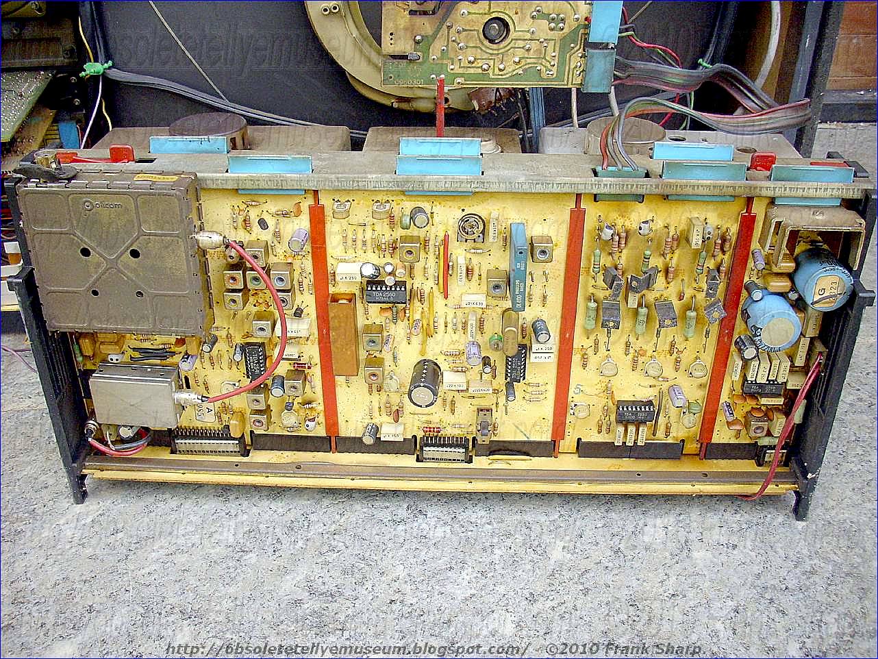


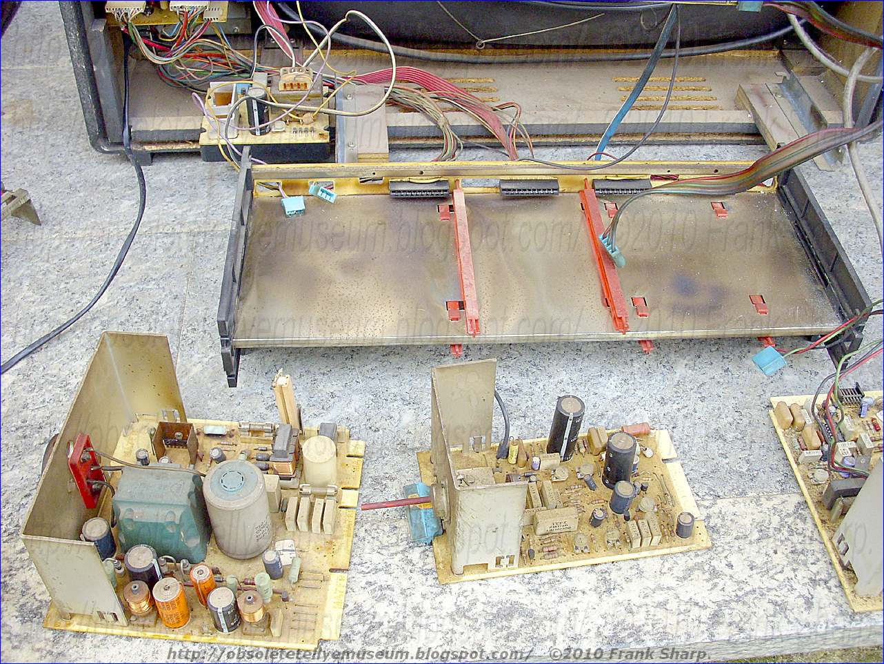


The units are fitted like "cards" above and under the chassis structure divided by power parts and signal parts.
Was first SINUDYNE adopting such chassis arrangement and first SINUDYNE using the PHILIPS 30AX SYSTEM CRT TUBE.
SINUDYNE TELECOMPUTER 2658 HIFI CHASSIS PROFESSIONAL 2000 Switched mode power supply
Supply is based on TDA4600 (SIEMENS).
Power supply Description based on TDA4601d (SIEMENS)

TDA4601 Operation. * The TDA4601 device is a single in line, 9 pin chip. Its predecessor was the TDA4600 device, the TDA4601 however has improved switching, better protection and cooler running. The (SIEMENS) TDA4601 power supply is a fairly standard parallel chopper switch mode type, which operates on the same basic principle as a line output stage. It is turned on and off by a square wave drive pulse, when switched on energy is stored in the chopper transformer primary winding in the form of a magnetic flux; when the chopper is turned off the magnetic flux collapses, causing a large back emf to be produced. At the secondary side of the chopper transformer this is rectified and smoothed for H.T. supply purposes. The advantage of this type of supply is that the high chopping frequency (20 to 70 KHz according to load) allows the use of relatively small H.T. smoothing capacitors making smoothing easier. Also should the chopper device go short circuit there is no H.T. output. In order to start up the TDA4601 I.C. an initial supply of 9v is required at pin 9, this voltage is sourced via R818 and D805 from the AC side of the bridge rectifier D801, also pin 5 requires a +Ve bias for the internal logic block. (On some sets pin 5 is used for standby switching). Once the power supply is up and running, the voltage on pin 9 is increased to 16v and maintained at this level by D807 and C820 acting as a half wave rectifier and smoothing circuit. PIN DESCRIPTIONS Pin 1 This is a 4v reference produced within the I.C. Pin 2 This pin detects the exact point at which energy stored in the chopper transformer collapses to zero via R824 and R825, and allows Q1 to deliver drive volts to the chopper transistor. It also opens the switch at pin 4 allowing the external capacitor C813 to charge from its external feed resistor R810. Pin 3 H.T. control/feedback via photo coupler D830. The voltage at this pin controls the on time of the chopper transistor and hence the output voltage. Normally it runs at Approximately 2v and regulates H.T. by sensing a proportion of the +4v reference at pin 1, offset by conduction of the photo coupler D830 which acts like a variable resistor. An increase in the conduction of transistor D830 and therefor a reduction of its resistance will cause a corresponding reduction of the positive voltage at Pin 3. A decrease
in this voltage will result in a shorter on time for the chopper transistor and therefor a lowering of the output voltage and vice versa, oscillation frequency also varies according to load, the higher the load the lower the frequency etc. should the voltage at pin 3 exceed 2.3v an internal flip flop is triggered causing the chopper drive mark space ratio to extend to 244 (off time) to 1 (on time), the chip is now in over volts trip condition. Pin 4 At this pin a sawtooth waveform is generated which simulates chopper current, it is produced by a time constant network R810 and C813. C813 charges when the chopper is on and is discharged when the chopper is off, by an internal switch strapping pin 4 to the internal +2v reference, see Fig 2. The amplitude of the ramp is proportional to chopper drive. In an overload condition it reaches 4v amplitude at which point chopper drive is reduced to a mark-space ratio of 13 to 1, the chip is then in over current trip. The I.C. can easily withstand a short circuit on the H.T. rail and in such a case the power supply simply squegs quietly. Pin 4 is protected by internal protection components which limit the maximum voltage at this pin to 6.5v. Should a fault occur in either of the time constant components, then the chopper transistor will probably be destroyed. Pin 5 This pin can be used for remote control on/off switching of the power supply, it is normally held at about +7v and will cause the chip to enter standby mode if it falls below 2v. Pin 6 Ground. Pin 7 Chopper switch off pin. This pin clamps the chopper drive voltage to 1.6v in order to switch off the chopper. Pin 8 Chopper base current output drive pin. Pin 9 L.T. pin, approximately 9v under start-up conditions and 16v during normal running, Current consumption of the I.C. is typically 135mA. The voltage at this pin must reach 6.7v in order for the chip to start-up.rth terminal of said control circuit delivering a sawtooth voltage being connected via a sixth resistance to a terminal of said primary winding of said transformer facing away from said transistor; a fifth terminal of said control circuit serving as a protective input being connected, via a seventh resistance to the cathode of said first diode and, through the intermediary of said seventh resistance and an eighth resistance, to the cathode of a third diode having an anode connected to an input of said rectifier circuit; a sixth terminal of said control circuit carrying said reference potential and being connected via a fourth capacitor to said fourth terminal of said control circuit and via a fifth capacitor to the anode of said second diode; a seventh terminal of said control circuit establishing a potential for pulses controlling said transistor being connected directly and an eighth terminal of said control circuit effecting pulse control of the base of said transistor being connected through the intermediary of a ninth resistance to said first capacitor leading to the base of said transistor; and a ninth terminal of said control circuit serving as a power supply input of said control circuit being connected both to the cathode of said first diode as well as via the intermediary of a sixth capacitor to a terminal of said second secondary winding as well as to a terminal of said third secondary winding.
Description:
The invention relates to a blocking oscillator type switching power supply for supplying power to electrical equipment, wherein the primary winding of a transformer, in series with the emitter-collector path of a first bipolar transistor, is connected to a d-c voltage obtained by rectification of a line a-c voltage fed-in via two external supply terminals, and a secondary winding of the transformer is provided for supplying power to the electrical equipment, wherein, furthermore, the first bipolar transistor has a base controlled by the output of a control circuit which is acted upon in turn by the rectified a-c line voltage as actual value and by a set-point transmitter, and wherein a starting circuit for further control of the base of the first bipolar transistor is provided. Such a blocking oscillator switching power supply is described in the German periodical, "Funkschau" (1975) No. 5, pages 40 to 44. It is well known that the purpose of such a circuit is to supply electronic equipment, for example, a television set, with stabilized and controlled supply voltages. Essential for such switching power supply is a power switching transistor i.e. a bipolar transistor with high switching speed and high reverse voltage. This transistor therefore constitutes an important component of the control element of the control circuit. Furthermore, a high operating frequency and a transformer intended for a high operating frequency are provided, because generally, a thorough separation of the equipment to be supplied from the supply naturally is desired. Such switching power supplies may be constructed either for synchronized or externally controlled operation or for non-synchronized or free-running operation. A blocking converter is understood to be a switching power supply in which power is delivered to the equipment to be supplied only if the switching transistor establishing the connection between the primary coil of the transformer and the rectified a-c voltage is cut off. The power delivered by the line rectifier to the primary coil of the transformer while the switching transistor is open, is interim-stored in the transformer and then delivered to the consumer on the secondary side of the transformer with the switching transistor cut off. In the blocking converter described in the aforementioned reference in the literature, "Funkschau" (1975), No. 5, Pages 40 to 44, the power switching transistor is connected in the manner defined in the introduction to this application. In addition, a so-called starting circuit is provided. Because several diodes are generally provided in the overall circuit of a blocking oscillator according to the definition provided in the introduction hereto, it is necessary, in order not to damage these diodes, that due to the collector peak current in the case of a short circuit, no excessive stress of these diodes and possibly existing further sensitive circuit parts can occur.
Considering the operation of a blocking oscillator, this means that, in the event of a short circuit, the number of collector current pulses per unit time must be reduced. For this purpose, a control and regulating circuit is provided. Simultaneously, a starting circuit must bring the blocking converter back to normal operation when the equipment is switched on, and after disturbances, for example, in the event of a short circuit. The starting circuit shown in the literature reference "Funkschau" on Page 42 thereof, differs to some extent already from the conventional d-c starting circuits. It is commonly known for all heretofore known blocking oscillator circuits, however, that a thyristor or an equivalent circuit replacing the thyristor is essential for the operation of the control circuit.
It is accordingly an object of the invention to provide another starting circuit. It is a further object of the invention to provide a possible circuit for the control circuit which is particularly well suited for this purpose. It is yet another object of the invention to provide such a power supply which is assured of operation over the entire range of line voltages from 90 to 270 V a-c, while the secondary voltages and secondary load variations between no-load and short circuit are largely constant. With the foregoing and other objects in view, there is provided, in accordance with the invention, a blocking oscillator-type switching power supply for supplying power to electrical equipment wherein a primary winding of a transformer, in series with an emitter-collector path of a first bipolar transistor, is connected to a d-c voltage obtained by rectification of a line a-c voltage fed-in via two external supply terminals, a secondary winding of the transformer being connectible to the electrical equipment for supplying power thereto, the first bipolar transistor having a base controlled by the output of a control circuit acted upon, in turn, by the rectified a-c line voltage as actual value and by a set-point transmitter, and including a starting circuit for further control of the base of the first bipolar transistor, including a first diode in the starting circuit having an anode directly connected to one of the supply terminals supplied by the a-c line voltage and a cathode connected via a resistor to an input serving to supply power to the control circuit, the input being directly connected to a cathode of a second diode, the second diode having an anode connected to one terminal of another secondary winding of the transformer, the other secondary winding having another terminal connected to the emitter of the first bipolar transmitter.
In accordance with another feature of the invention, there is provided a second bipolar transistor having the same conduction type as that of the first bipolar transistor and connected in the starting circuit with the base thereof connected to a cathode of a semiconductor diode, the semiconductor diode having an anode connected to the emitter of the first bipolar transistor, the second bipolar transistor having a collector connected via a resistor to a cathode of the first diode in the starting circuit, and having an emitter connected to the input serving to supply power to the control circuit and also connected to the cathode of the second diode which is connected to the other secondary winding of the transformer.
In accordance with a further feature of the invention, the base of the second bipolar transistor is connected to a resistor and via the latter to one pole of a first capacitor, the anode of the first diode being connected to the other pole of the first capacitor.
In accordance with an added feature of the invention, the input serving to supply power to the control circuit is connected via a second capacitor to an output of a line rectifier, the output of the line rectifier being directly connected to the emitter of the first bipolar transistor.
In accordance with an additional feature of the invention, the other secondary winding is connected at one end to the emitter of the first bipolar transistor and to a pole of a third capacitor, the third capacitor having another pole connected, on the one hand, via a resistor, to the other end of the other secondary winding and, on the other hand, to a cathode of a third diode, the third diode having an anode connected via a potentiometer to an actual value input of the control circuit and, via a fourth capacitor, to the emitter of the first bipolar transistor.
In accordance with yet another feature of the invention, the control circuit has a control output connected via a fifth capacitor to the base of the first bipolar transistor for conducting to the latter control pulses generated in the control circuit.
In accordance with a concomitant feature of the invention, there is provided a sixth capacitor shunting the emitter-collector path of the first transistor.
Other features which are considered as characteristic for the invention are set forth in the appended claim.
The construction and method of operation of the invention, however, together with additional objects and advantages thereof will be best understood from the following description of specific embodiments when read in connection with the accompanying drawings, in which:
FIGS. 1 and 2 are circuit diagrams of the blocking oscillator type switching power supply according to the invention; and
FIG. 3 is a circuit diagram of the control unit RS of FIGS. 1 and 2.
Referring now to the drawing and, first, particularly to FIG. 1 thereof, there is shown a rectifier circuit G in the form of a bridge current, which is acted upon by a line input represented by two supply terminals 1' and 2'. Rectifier outputs 3' and 4' are shunted by an emitter-collector path of an NPN power transistor T1 i.e. t
 he
series connection of the so-called first bipolar transistor referred to
hereinbefore with a primary winding I of a transformer Tr. Together
with the inductance of the transformer Tr, the capacitance C1 determines
the frequency and limits the opening voltages of the switch embodied by
the first transistor T1. A capacitance C2, provided between the base of
the first transistor T1 and the control output 7,8 of a control circuit
RS, separates the d-c potentials of the control or regulating circuit
RS and the switching transistor T1 and serves for addressing this
switching transistor T1 with pulses. A resistor R1 provided at the
control output 7,8 of the control circuit RS is the negative-feedback
resistor of both output stages of the control circuit RS. It determines
the maximally possible output pulse current of the control circuit RS. A
secondary winding II of the transformer Tr takes over the power supply
of the control circuit, in steady state operation, via the diode D1. To
this end, the cathode of this diode D1 is directly connected to a power
supply input 9 of the control circuit RS, while the anode thereof is
connected to one terminal of the secondary winding II. The other
terminal of the secondary winding II is connected to the emitter of the
power switching transistor T1.
he
series connection of the so-called first bipolar transistor referred to
hereinbefore with a primary winding I of a transformer Tr. Together
with the inductance of the transformer Tr, the capacitance C1 determines
the frequency and limits the opening voltages of the switch embodied by
the first transistor T1. A capacitance C2, provided between the base of
the first transistor T1 and the control output 7,8 of a control circuit
RS, separates the d-c potentials of the control or regulating circuit
RS and the switching transistor T1 and serves for addressing this
switching transistor T1 with pulses. A resistor R1 provided at the
control output 7,8 of the control circuit RS is the negative-feedback
resistor of both output stages of the control circuit RS. It determines
the maximally possible output pulse current of the control circuit RS. A
secondary winding II of the transformer Tr takes over the power supply
of the control circuit, in steady state operation, via the diode D1. To
this end, the cathode of this diode D1 is directly connected to a power
supply input 9 of the control circuit RS, while the anode thereof is
connected to one terminal of the secondary winding II. The other
terminal of the secondary winding II is connected to the emitter of the
power switching transistor T1.The cathode of the diode D1 and, therewith, the power supply terminal 9 of the control circuits RS are furthermore connected to one pole of a capacitor C3, the other pole of which is connected to the output 3' of the rectifier G. The capacitance of this capacitor C3 thereby smoothes the positive half-wave pulses and serves simultaneously as an energy storage device during the starting period. Another secondary windi
 ng
III of the transformer Tr is connected by one of the leads thereof
likewise to the emitter of the first transistor T1, and by the other
lead thereof via a resistor R2, to one of the poles of a further
capacitor C4, the other pole of which is connected to the
first-mentioned lead of the other secondary winding III. This second
pole of the capacitor C4 is simultaneously connected to the output 3' of
the rectifier circuit G and, thereby, via the capacitor C3, to the
cathode of the diode D1 driven by the secondary winding II of the
transformer Tr as well as to the power supply input 9 of the control
circuit RS and, via a resistor R9, to the cathode of a second diode D4.
The second pole of the capacitor C4 is simultaneously connected directly
to the terminal 6 of the control circuit RS and, via a further
capacitor C 6, to the terminal 4 of the control circuit RS as well as,
additionally, via the resistor R6, to the other output 4' of the
rectifier circuit G. The other of the poles of the capacitor C4 acted
upon by the secondary winding II is connected via a further capacitor C5
to a node, which is connected on one side thereof, via a variable
resistor R4, to the terminals 1 and 3 of the control circuit RS, with
the intermediary of a fixed resistor R5 in the case of the terminal 1.
On the other side of the node, the latter and, therefore, the capacitor
C5 are connected to the anode of a third diode D2, the cathode of which
is connected on the one hand, to the resistor R2 mentioned hereinbefore
and leads to the secondary winding III of the transformer Tr and, on the
other hand, via a resistor R3 to the terminal 2 of the control circuit
RS.
ng
III of the transformer Tr is connected by one of the leads thereof
likewise to the emitter of the first transistor T1, and by the other
lead thereof via a resistor R2, to one of the poles of a further
capacitor C4, the other pole of which is connected to the
first-mentioned lead of the other secondary winding III. This second
pole of the capacitor C4 is simultaneously connected to the output 3' of
the rectifier circuit G and, thereby, via the capacitor C3, to the
cathode of the diode D1 driven by the secondary winding II of the
transformer Tr as well as to the power supply input 9 of the control
circuit RS and, via a resistor R9, to the cathode of a second diode D4.
The second pole of the capacitor C4 is simultaneously connected directly
to the terminal 6 of the control circuit RS and, via a further
capacitor C 6, to the terminal 4 of the control circuit RS as well as,
additionally, via the resistor R6, to the other output 4' of the
rectifier circuit G. The other of the poles of the capacitor C4 acted
upon by the secondary winding II is connected via a further capacitor C5
to a node, which is connected on one side thereof, via a variable
resistor R4, to the terminals 1 and 3 of the control circuit RS, with
the intermediary of a fixed resistor R5 in the case of the terminal 1.
On the other side of the node, the latter and, therefore, the capacitor
C5 are connected to the anode of a third diode D2, the cathode of which
is connected on the one hand, to the resistor R2 mentioned hereinbefore
and leads to the secondary winding III of the transformer Tr and, on the
other hand, via a resistor R3 to the terminal 2 of the control circuit
RS.The nine terminals of the control circuit RS have the following purposes or functions:
Terminal 1 supplies the internally generated reference voltage to ground i.e. the nominal or reference value required for the control or regulating process;
Terminal 2 serves as input for the oscillations provided by the secondary winding III, at the zero point of which, the pulse start of the driving pulse takes place;
Terminal 3 is the control input, at which the existing actual value is communicated to the control circuit RS, that actual value being generated by the rectified oscillations at the secondary winding III;
Terminal 4 is responsive to the occurrence of a maximum excursion i.e. when the largest current flows through the first transistor T1 ;
Terminal 5 is a protective input which responds if the rectified line voltage drops too sharply; Terminal 6 serves for the power supply of the control process and, indeed, as ground terminal;
Terminal 7 supplies the d-c component required for charging the coupling capacitor C2 leading to the base of the first transistor T1 ;
Terminal 8 supplies the control pulse required for the base of the first transistor T1 ; and
Terminal 9 serves as the first terminal of the power supply of the control circuit RS.
Further details of the control circuit RS are described hereinbelow.
The capacity C3 smoothes the positive half-wave pulses which are provided by the secondary winding II, and simultaneously serves as an energy storage device during the starting time. The secondary winding III generates the control voltage and is simultaneously used
as
feedback. The time delay stage R2 /C4 keeps harmonics and fast
interference spikes away from the control circuit RS. The resistor R3 is
provided as a voltage divider for the second terminal of the control
circuit RS. The diode D2 rectifies the control pulses delivered by the
secondary winding III. The capacity C5 smoothes the control voltage. A
reference voltage Uref, which is referred to ground i.e. the potential
of terminal 6 is present at the terminal 1 of the control circuit RS.
The resistors R4 and R5 form a voltage divider of the input-difference
control amplifier at the terminal 3. The desired secondary voltage can
be set manually via the variable resistor R4. A time-delay stage R6 /C6
forms a sawtooth rise which corresponds to the collector current rise of
the first bipolar transistor T1 via the primary winding I of the
transformer Tr. The sawtooth present at the terminal 4 of the control
circuit RS is limited there between the reference voltage 2 V and 4 V.
The voltage divider R7 /R8 (FIG. 2), brings to the terminal 5 of the
control circuit RS the enabling voltage for the drive pulse at the
output 8 of the control circuit RS.
The diode D4, together with the resistor R9 in cooperation with the diode D1 and the secondary winding II, forms the starting circuit provided, in accordance with the invention. The operation thereof is as follows:
After the switching power supply is switched on, d-c voltages build up at the collector of the switching transistor T1 and at the input 4 of the control circuit RS, as a function in time of the predetermined time constants. The positive sinusoidal half-waves charge the capacitor C3 via the starting diode D4 and the starting resistor R9 in dependence upon the time constant R9.C3. Via the protective input terminal 5 and the resisto
r
R11 not previously mentioned and forming the connection between the
resistor R9 and the diode D1, on the one hand, and the terminal 5 of the
control circuit RS, on the other hand, the control circuit RS is biased
ready for switching-on, and the capacitor C2 is charged via the output
7. When a predetermined voltage value at the capacitor C3 or the power
supply input 9 of the control circuit RS, respectively, is reached, the
reference voltage i.e. the nominal value for the operation of the
control voltage RS, is abruptly formed, which supplies all stages of the
control circuit and appears at the output 1 thereof. Simultaneously,
the switching transistor T1 is switched into conduction via the output
8. The switching of the transistor T1 at the primary winding T of the
transformer Tr is transformed to the second secondary winding II, the
capacity C3 being thereby charged up again via the diode D1. If
sufficient energy is stored in the capacitor C3 and if the re-charge via
the diode D1 is sufficient so that the voltage at a supply input 9 does
not fall below the given minimum operating voltage, the switching power
supply then remains connected, so that the starting process is
completed. Otherwise, the starting process described is repeated several
times.In FIG. 2, there is shown a further embodiment of the circuit for a blocking oscillator type switching power supply, according to the invention, as shown in FIG. 1. Essential for this circuit of FIG. 2 is the presence of a second bipolar transistor T2 of the type of the first bipolar transistor T1 (i.e. in the embodiments of the invention, an npn-transistor), which forms a further component of the starting circuit and is connected with the collector-emitter path thereof between the resistor R9 of the starting circuit and the current supply input 9 of the control circuit RS. The base of this second transistor T2 is connected to a node which leads, on the one hand, via a resistor R10 to one electrode of a capacitor C7, the other electrode of which is connected to the anode of the diode D4 of the starting circuit and, accordingl
 y,
to the terminal 1' of the supply input of the switching power supply G.
On the other hand, the last-mentioned node and, therefore, the base of
the second transistor T2 are connected to the cathode of a Zener diode
D3, the anode of which is connected to the output 3' of the rectifier G
and, whereby, to one pole of the capacitor C3, the second pole of which
is connected to the power supply input 9 of the control circuit RS as
well as to the cathode of the diode D1 and to the emitter of the second
transistor T2. In other respects, the circuit according to FIG. 2
corresponds to the circuit according to FIG. 1 except for the resistor
R11 which is not necessary in the embodiment of FIG. 2, and the missing
connection between the resistor R9 and the cathode of the diode D1,
respectively, and the protective input 5 of the control circuit RS.
y,
to the terminal 1' of the supply input of the switching power supply G.
On the other hand, the last-mentioned node and, therefore, the base of
the second transistor T2 are connected to the cathode of a Zener diode
D3, the anode of which is connected to the output 3' of the rectifier G
and, whereby, to one pole of the capacitor C3, the second pole of which
is connected to the power supply input 9 of the control circuit RS as
well as to the cathode of the diode D1 and to the emitter of the second
transistor T2. In other respects, the circuit according to FIG. 2
corresponds to the circuit according to FIG. 1 except for the resistor
R11 which is not necessary in the embodiment of FIG. 2, and the missing
connection between the resistor R9 and the cathode of the diode D1,
respectively, and the protective input 5 of the control circuit RS.Regarding the operation of the starting circuit according to FIG. 2,
 it can be stated that the positive sinusoidal half-wave of the line
voltage, delayed by the time delay stage C7, R10 drives the base of the
transistor T2 in the starting circuit. The amplitude is limited by the
diode D3 which is provided for overvoltage protection of the control
circuit RS and which is preferably incorporated as a Zener diode. The
second transistor T2 is switched into conduction. The capacity C3 is
charged, via the serially connected diode D4 and the resistor R9 and the
collector-emitter path of the transistor T2, as soon as the voltage
between the terminal 9 and the terminal 6 of the control circuit RS i.e.
the voltage U9, meets the condition U9 <[UDs -UBE (T2)].
it can be stated that the positive sinusoidal half-wave of the line
voltage, delayed by the time delay stage C7, R10 drives the base of the
transistor T2 in the starting circuit. The amplitude is limited by the
diode D3 which is provided for overvoltage protection of the control
circuit RS and which is preferably incorporated as a Zener diode. The
second transistor T2 is switched into conduction. The capacity C3 is
charged, via the serially connected diode D4 and the resistor R9 and the
collector-emitter path of the transistor T2, as soon as the voltage
between the terminal 9 and the terminal 6 of the control circuit RS i.e.
the voltage U9, meets the condition U9 <[UDs -UBE (T2)].Because of the time constant R9.C3, several positive half-waves are necessary in order to increase the voltage U9 at the supply terminal 9 of the control circuit RS to such an extent that the control circuit RS is energized. During the negative sine half-wave, a partial energy chargeback takes place from the capacitor C3 via the emitter-base path of the transistor T2 of the starting circuit and via the resistor R10 and the capacitor C7, respectively, into the supply network. At approximately 2/3 of the voltage U9, which is limited by the diode D3, the control circuit RS is switched on. At the terminal 1 thereof, the reference voltage Uref then appears. In addition, the voltage divider R5 /R4 becomes effective. At the terminal 3, the control amplifier receives the voltage forming the actual value, while the first bipolar transistor T1 of the blocking-oscillator type switching power supply is addressed pulsewise via the terminal 8.
Because the capacitor C6 is charged via the resistor R6, a higher voltage than Uref is present at the terminal 4 if the control circuit RS is activated. The control voltage then discharges the capacitor C6 via the terminal 4 to half the value of the reference voltage Uref, and immediately cuts off the addressing input 8 of the control circuit RS. The first driving pulse of the switching transistor T1 is thereby limited to a minimum of time. The power for switching-on the control circuit RS and for driving the transistor T1 is supplied by the capacitor C3. The voltage U9 at the capacitor C3 then drops. If the voltage U9 drops below the switching-off voltage value of the control circuit RS, the latter is then inactivated. The next positive sine half-wave would initiate the starting process again.
By switching the transistor T1, a voltage is transformed in the secondary winding II of the transformer Tr. The positive component is rectified by the diode D1, recharing of the capacitor C3 being thereby provided. The voltage U9 at the output 9 does not, therefore, drop below the minimum value required for the operation of the control circuit RS, so that the control circuit RS remains activated. The power supply continues to operate in the rhythm of the existing conditions. In operation, the voltage U9 at the supply terminal 9 of the control circuit RS has a value which meets the condition U9 >[UDs -UBE (T2)], so that the transistor T2 of the starting circuit remains cut off.
For the internal layout of the control circuit RS, the construction shown, in particular, from FIG. 3 is advisable. This construction is realized, for example, in the commercially available type TDA 4600 (Siemens AG).
The block diagram of the control circuit according to FIG. 3
 shows
the power supply thereof via the terminal 9, the output stage being
supplied directly whereas all other stages are supplied via Uref. In the
starting circuit, the individual subassemblies are supplied with power
sequentially. The d-c output voltage potential of the base current gain
i.e. the voltage for the terminal 8 of the control circuit RS, and the
charging of the capacitor C2 via the terminal 7 are formed even before
the reference voltage Uref appears. Variations of the supply voltage U9
at terminal 9 and the power fluctuations at the terminal 8/terminal 7
and at the terminal 1 of the control circuit RS are leveled or smoothed
out by the voltage control. The temperature sensitivity of the control
circuit RS and, in particular, the uneven heating of the output and
input stages and input stages on the semiconductor chip containing the
control circuit in monolithically integrated form are intercepted by the
temperature compensation provided. The output values are constant in a
specific temperature range. The message for blocking the output stage,
if the supply voltage at the terminal 9 is too low, is given also by
this subassembly to a provided control logic.
shows
the power supply thereof via the terminal 9, the output stage being
supplied directly whereas all other stages are supplied via Uref. In the
starting circuit, the individual subassemblies are supplied with power
sequentially. The d-c output voltage potential of the base current gain
i.e. the voltage for the terminal 8 of the control circuit RS, and the
charging of the capacitor C2 via the terminal 7 are formed even before
the reference voltage Uref appears. Variations of the supply voltage U9
at terminal 9 and the power fluctuations at the terminal 8/terminal 7
and at the terminal 1 of the control circuit RS are leveled or smoothed
out by the voltage control. The temperature sensitivity of the control
circuit RS and, in particular, the uneven heating of the output and
input stages and input stages on the semiconductor chip containing the
control circuit in monolithically integrated form are intercepted by the
temperature compensation provided. The output values are constant in a
specific temperature range. The message for blocking the output stage,
if the supply voltage at the terminal 9 is too low, is given also by
this subassembly to a provided control logic.The outer voltage divider of the terminal 1 via the r
esistors
R5 and R4 to the control tap U forms, via terminal 3, the variable side
of the bridge for the control amplifier formed as a differential
amplifier. The fixed bridge side is formed by the reference voltage Uref
via an internal voltage divider. Similarly formed are circuit portions
serving for the detection of an overload short circuit and circuit
portions serving for the "standby" no-load detection, which can be
operated likewise via terminal 3.
Within a provided trigger circuit, the driving pulse length is determined as a function of the sawtooth rise at the terminal 4, and is transmitted to the control logic. In the control logic, the commands of the trigger circuit are processed. Through the zero-crossing identification at input 2 in the control circuit RS, the control logic is enabled to start the control input only at the zero point of the frequency oscillation. If the voltages at the terminal 5 and at the terminal 9 are too low, the control logic blocks the output amplifier at the terminal 8. The output amplifier at the terminal 7 which is responsible for the base charge in the capacitor C2, is not touched thereby.
The base current gain for the transistor T1 i.e. for the first transistor in accordance with the definition of the invention, is formed by two amplifiers which mutually operate on the capacitor C2. The roof inclination of the base driving current for the transistor T1 is impressed by the collector current simulation at the terminal 4 to the amplifier at the terminal 8. The control pulse for the transistor T1 at the terminal 8 is always built up to the potential present at the terminal 7. The amplifier working into the terminal 7 ensures that each new switching pulse at the terminal 8 finds the required base level at terminal 7.
Supplementing the comments regarding FIG. 1, it should also be mentioned that the cathode of the diode D1 connected by the anode thereof to the one end of the secondary winding II of the transformer Tr is connected via a resistor R11 to the protective input 5 of the control circuit RS whereas, in the circuit according to FIG. 2, the protective input 5 of the control circuit RS is supplied via a voltage divider R8, R7 directly from the output 3', 4' of the rectifier G delivering the rectified line a-c voltage, and which obtains the voltage required for executing its function. It is evident that the first possible manner of driving the protective input 5 can be used also in the circuit according to FIG. 2, and the second possibility also in a circuit in accordance with FIG. 1.
The control circuit RS which is shown in FIG. 3 and is realized in detail by the building block TDA 4600 and which is particularly well suited in conjunction with the blocking oscillator type switching power supply according to the invention has 9 terminals 1-9, which have the following characteristics, as has been explained in essence hereinabove:
Terminal 1 delivers a reference voltage Uref which serves as the constant-current source of a voltage divider R5.R4 which supplies the required d-c voltages for the differential amplifiers provided for the functions control, overload detection, short-circuit detection and "standby"-no load detection. The dividing point of the voltage divider R5 -R4 is connected to the terminal 3 of the control circuit RS. The terminal 3 provided as the control input of RS is controlled in the manner described hereinabove as input for the actual value of the voltage to be controlled or regulated by the secondary winding III of the transformer Tr. With this input, the lengths of the control pulses for the switching transistor T1 are determined.
Via the input provided by the terminal 2 of the control circuit RS, the zero-point identification in the control circuit is addressed for detecting the zero-point o
f
the oscillations respectively applied to the terminal 2. If this
oscillation changes over to the positive part, then the addressing pulse
controlling the switching transistor T1 via the terminal 8 is released
in the control logic provided in the control circuit.A sawtooth-shaped voltage, the rise of which corresponds to the collector current of the switching transistor T1, is present at the terminal 4 and is minimally and maximally limited by two reference voltages. The sawtooth voltage serves, on the one hand as a comparator for the pulse length while, on the other hand, the slope or rise thereof is used to obtain in the base current amplification for the switching transistor T1, via the terminal 8, a base drive of this switching transistor T1 which is proportional to the collector current.
The terminal 7 of the control circuit RS as explained hereinbefore, determines the voltage potential for the addressing pulses of the transistor T2. The base of the switching transistor T1 is pulse-controlled via the terminal 8, as described hereinbefore. Terminal 9 is connected as the power supply input of the control circuit RS. If a voltage level falls below a given value, the terminal 8 is blocked. If a given positive value of the voltage level is exceeded, the control circuit is activated. The terminal 5 releases the terminal 8 only if a given voltage potential is present.
Foreign References:
DE2417628A1 1975-10-23 363/37 DE2638225A1 1978-03-02 363/49
Other References:
Grundig Tech. Info. (Germany), vol. 28, No. 4, (1981).
IBM Technical Disclosure Bulletin, vol. 19, No. 3, pp. 978, 979, Aug. 1976.
German Periodical, "Funkschau", (1975), No. 5, pp. 40 to 44.
Inventors:
Peruth, Gunther (Munich, DE) Siemens Aktiengesellschaft (Berlin and Munich, DE)TDA2530 RGB MATRIX PREAMPLIFIER
The TDA2530 is an integrated RGB -matrix preamplifier for colour television receivers,
incorporating a matrix preamplifier for RGB cathode drive of the picture tube with
clamping circuits.
 The three channels have the same layout to ensure identical frequency
behaviour.
This integrated circuit has been designed to be driven from the TDA2522 Synchronous
demodulator and oscillator IC.
TDA2522 PAL TV CHROMA DEMODULATOR COMBINATION
FAIRCHILD LINEAR INTEGRATED CIRCUIT
GENERAL DESCRIPTION- The TDA2522 is a monolithic integrated circuit designed as
a synchronous demodulator for PAL color television receivers. It includes an 8,8 MHz

oscillator and divider to generate two 4.4 MHz reference signals and provides color difference outputs.
PACKAGE OUTLINE 9B
The TDA2522 is Intended to Interface directly with the TDA2560 with a minimum oF external components. The TDA2530 may be added if RGB drive is required. The TDA2522
is constructed using the Fairchild Planar* process.
TDA2560 LUMINANCE AND CHROMINANCE CONTROL COMBINATION
The TDA2560 is a monolithic integrated circuit for use in decoding systems of COLORtelevision receivers. The circuit consists of a luminance and chrominance amplifier.
The luminance amplifier has a low input impedance so that matching of the luminance
delay line is very easy.
It also incorporates the following functions:
- d.c. contrast control;

- d.c. brightness control;
- black level clamp;
- blanking;
- additional video output with positive-going sync.
The chrominance amplifier comprises:
- gain controlled amplifier;
- chrominance gain control tracked with contrast control;
- separate d.c. saturation control:
- combined chroma and burst output, burst signal amplitude not affected by contrast and
saturation control;
- the delay line can be driven directly ‘by the IC.
APPLICATION INFORMATION (continued)
The function is quoted against the corresponding pin number
Balanced chrominance input signal (in conjunction with pin 2)
This is derived from the chrominance signal bandpass filter, designed to provide a
push-pull input. A signal amplitude of at least 4 mV peak-to-peak is required
between pins l and 2. The chrominance amplifier is stabilized by an external feedback
loop from the output (pin 6) to the input (pins I and 2). The required level at pins l
and 2 will be 3 V.
All figures for the chrominance signals are based on a colour bar signal with 75%
saturation: i.e. burst-to-chrominance ratio of input signal is 1 1 2.
Chrominance signal input (see pin 1)
A. C.C. input
A negative-going potential, starting at +l,2 V, gives a 40 dB range of a. c. c.
Maximum gain reduction is achieved at an input voltage of 500 mV.
Chrominance saturation control
A control range of +6 dB to >-14 dB is provided over a range of d. c. potential on
pin 4 from +2 to +4 V. The saturation control is a linear function of the control
voltage.
Negative supply (earth)
Chro minance signal output
For nominal settings of saturation and contrast controls (max. -6 dB for saturation,
and max. -3 dB for contrast) both the chroma' and burst are available at this pin, and
in the same ratio as at the input pins 1 and 2. The burst signal is not affected by the
saturation and contrast controls. The a.c. c. circuit of the TDA2522 will hold
constant the colour burst amplitude at the input of the TDA2522. As the PAL delay
line is situated here between the TDA256O and TDA2522 there may be some variation
of the nominal 1 V peak-to-peak burst output of the TDA2560, according to the
tolerances of the delay line. An external network is required from pin 6 of the
TDA256O to provide d. c. negative feedback in the chroma channel via pins I and 2.
Burst gating and clamping pulse input
A two-level pulse is required at this pin to be used for burst gate and black level
clamping. The black level clamp is activated when the pulse level is greater than
7 V. The timing of this interval should be such that no appreciable encroachment
occurs into the sync pulse on picture line periods during normal operation of the
receiver. The burst gate, which switches the gain of the chroma amplifier to
maximum, requires that the input pulse at pin 7 should be sufficiently wide, at least
8 ps, at the actuating level of 2,3 V.
Correct operation occurs within the range 10 to 14 V. All signal and control levels
have a linear dependency on supply voltage but, in any given receiver design, this
range may be restricted due to considerations of tracking between the power supply
variations and picture contrast and chroma levels.
Flyback blanking input waveform
This pin is used for blanking the luminance amplifier. When the input pulse exceeds
the +2, 5 Vlevel, the output signal is blanked to a level of about 0 V. When the input
exceeds a +6 V level, a fixed level of about 1, 5 V is inserted in the output. This
level can be used for clamping purposes.
Luminance sigal output
An emitter follower provides a low impedance output signal of 3 V black-to-white
amplitude at nominal contrast setting having a black level in the range 1 to 3 V. An
external emitter load resistor is not required.
to the resistor value from pin 13 to the +12 V supply. At an input bias current
114 of 0,25 mA during black level the amplifier is compensated so that no black
level shift more than 10 mV occurs at contrast control. When the input current
deviates from the quoted value the black level shift amounts to 100 mV/rnA.
Brightness control
The black level at the luminance output (pin 10) is identical to the control voltage
required at this pin, A range of black level from l to 3 V may be obtained.
Black level clamp capacitor
Luminance gain setting resistor
The gain of the luminance amplifier may be adjusted by selection of the resistor
value from pin 13 to +12 V. Nominal luminance output amplitude is then 3 V
black-to-white at pin 10 when this resistor is 2, 7
TDA2591 SYNCHRO AND HORIZONTAL DEFLECTION CONTROL FOR COLOR TV SET
DESCRIPTION
The TDA2591 is a circuit intended for the horizontal
deflection of color TVsets, supplied with transistors
or SCR’S.
oscillator ‘_circuits for colour television receivers using
thyristor or transistor line deflection output stages.
The _circuits incorporate a line oscillator ‘which is
based on the threshold switching principle, a line de-
flection output stage capable of direct drive of thyristor
deflection circuits, phase comparison between the
oscillator voltage and both the sync pulse and line
flyback pulse. Also included on the chip is a switch for
changing the filter characteristic and the gate circuit
when used for VCR.
The TDA2593 generates a sandcastle pulse (at pin
7) suitable for use with the TDA.2532.
.LINE OSCILLATOR(two levels switching)
.PHASE COMPARISON BETWEEN SYNCHRO-
PULSE AND OSCILLATOR VOLTAGE Ø 1, ENABLED BY AN INTERNAL PULSE,
(better parasitic immunity)
PHASE COMPARISON BETWEEN THE FLYBACK
PULSES AND THE OSCILLATOR VOLTAGE Ø2
.COINCIDENCE DETECTOR PROVIDING A LARGE HOLD-IN-RANGE.
.FILTER CHARACTERISTICS AND GATE SWITCHING FOR VIDEO RECORDER APPLICATION.
.NOISE GATED SYNCHRO SEPARATOR
.FRAME PULSE SEPARATOR .BLANKING AND SAND CASTLE OUTPUT PULSES
.HORIZONTAL POWER STAGE PHASE LAGGING CIRCUIT
.SWITCHING OF CONTROL OUTPUT PULSE WIDTH
.SEPARATED SUPPLY VOLTAGE OUTPUT STAGE ALLOWING DIRECT DRIVE OF SCR’S CIRCUITS.
.SECURITY CIRCUIT MAKES THE OUTPUT PULSE SUPPRESSED WHEN LOW SUPPLY
VOLTAGE.
TDA2541 IF AMPLIFIER WITH DEMODULATOR AND AFC
 DESCRIPTION
The TDA2540 and 2541 are IF amplifier and A.M.
demodulator circuits for colour and black and white
television receivers using PNP or NPN tuners. They
are intended for reception of negative or positive
modulation CCIR standard.
They incorporate the following functions : .Gain controlled amplifier .Synchronous demodulator .White spot inverter .Video preamplifier with noise protection .Switchable AFC .AGC with noise gating .Tuner AGC output (NPN tuner for 2540)-(PNP
tuner for 2541) .VCR switch for video output inhibition (VCR
play back).An automatic fine tuning (AFT) circuit is provided which generates an AFT control signal in response to a video intermediate frequency (I.F.) signal. The I.F. signal is supplied to the inputs of two buffer amplifiers, which couple signals of like phase relationship to two inputs of a discriminator network. The discriminator network is tuned to the desired frequency of the video I.F. signal, and is responsive to the buffered I.F. signals for causing respective signal voltages to be developed at its inputs which vary differentially in magnitude in response to the frequency deviation of the I.F. signals from the desired I.F. frequency. The differentially related signals are detected by two peak detector networks for use as AFT control signals. The buffer amplifiers and peak detectors may be conveniently fabricated on a single I.C. chip. The discriminator network is coupled to the buffer amplifiers by two external I.C. terminals.
SINUDYNE TELECOMPUTER 2658 THOR HIFI CHASSIS PROFESSIONAL 2000 Digital phase locked loop tuning system / PLL FREQUENCY SYNTHESIZER:


programmable divider means coupled to said programming means being responsive to said first, second digital control signals and the local oscillator signal, in a local oscillator mode, for generating the digital output signal which is representative of a desired frequency corresponding to said selected channel number, said programmable divider means including means for dividing the local oscillator signal by first and second factors, said first factor being related to the frequency separation between local oscillator signals by an integral number, the local oscillator signal being divided by said first factor during a first interval for a first number of periods of the output signal and being divided by said second factor for a second number of periods of the output signal, said first number of periods being related to the number of the channel selected, said second number being related to the channel group within which the selected channel lies.
2. Phase locked loop system according to claim 1, wherein said programming means including means coupled to said programming means for receiving an MFT signal and being responsive to said MFT signal for altering said first and second digital control signals, and said programmable divider means being responsive to said altered digital control signals for generating an altered system output frequency. 3. Phase locked loop system according to claim 2, wherein said programming means includes first terminal means coupled to said programming means for receiving an AFT control signal, and first logic means responsive to the input signal and the AFT control signal for generating the first digital control signal. 4. Phase locked loop system according to claim 3, wherein said programming means includes second logic means coupled to said first logic means and responsive to the AFT control signal for generating the second digital control signal. 5. Phase locked loop system according to claim 4, wherein said second logic means includes group decoder means coupled to said first logic means. 6. Phase locked loop circuit means according to claim 5, wherein said second logic means includes memory means coupled to said group decoder means and to said first terminal means. 7. Phase locked loop system according to claim 6, wherein said second logic means includes second terminal means for receiving an MFT signal, and up/down counter latch means coupled to said memory means and to said second terminal means for altering said first and second digital control signals in response to said MFT signal. 8. Phase locked loop system according to claim 7, wherein said second logic means includes adder means coupled to said up/down counter latch means to said memory means. 9. Phase locked loop system according to claim 3, wherein said first logic means includes channel number generator means coupled to said first terminal means and responsive to said input signal. 10. Phase locked loop system according to claim 9, wherein said channel number generator means includes first and second data selector means coupled to said first terminal means, and adder means coupled to said second data selector means and to said up/down counter latch means. 11. Phase locked loop system according to claim 1, wherein said means for dividing the local oscillator signal includes programmable counter means for generating a modulus control output signal, and variable modulus prescaler divider means coupled to and responsive to said programmable counter means, said variable modulus prescaler divider means dividing the local oscillator signal by said first and second factors. 12. Phase locked loop syst
em according to claim 11, wherein said programmable counter means includes third data selector means coupled to receive said first and second digital control signals and said modulus control signal. 13. Phase locked loop system according to claim 12, wherein said programmable counter means includes a programmable counter coupled to said third data selector means and to said variable modulus prescaler divider means. 14. Phase locked loop system according to claim 13, wherein said programmable counter means includes look ahead circuit means coupled to said programmable counter, and divide by two circuit means coupled to said look ahead circuit means for generating said modulus control output signal. 15. Phase locked loop tuning system according to claim 1 including digital automatic fine tuning (AFT) means wherein: said programmable divider means includes switching means responsive to an AFT control signal to inhibit the local oscillator signal to said programmable divider means and to provide an input signal thereto of a different frequency than the local oscillator signal; and
said programming means including logic means responsive to said AFT control signal for altering said first and second digital control signals to predetermined values to cause the phase locked loop tuning system to be operable in an automatic fine tuning mode.
16. Phase locked loop tuning system of claim 15 wherein said programmable divider means includes:
programmable counter means for generating first and second modulus control signals; and
dual modulus prescaler means responsive to said first modulus control signal for dividing the local oscillator signal in said local oscillator mode and said input signal of a different frequency in said automatic fine tuning mode by said first factor which is equal to the integer six and being responsive to said second modulus control signal for dividing said local oscillator signal and said input signal of a different frequency by said second factor which is equal to the integer five respectively.
17. Phase locked loop tuning system of claim 16 wherein said signal of a different frequency is an intermediate frequency signal provided by the tuning system and supplied to said switching means.
variable modulus divider means for selectively dividing the frequency of the local oscillator signal by first and second factors in response to a modulus control signal to provide an output signal, said first factor being related to the frequency separation between local oscillator signals by an integral number; and
programmable means for generating said modulus control signal to cause said variable modulus divider means to divide by said first factor during a first interval for a first number of periods of said output signal and to divide by said second
factor during a second interval for a second number of periods of said output signal, said first number of periods being related to the number of the channel selected, said second number of periods being related to the channel group corresponding to the selected channel.20. The phase locked loop tuning system of claim 19 wherein said programmable means includes:
programming means responsive to a selected channel input signal for producing first and second digital output signals, said first digital output signal being related to the selected channel number plus one of two constant values which are determined in accordance within which channel group the selected channel input signal lies, said second digital signal being a constant value for all selected channels within a channel group; and
programmable divider means responsive to said first and second digital output signals from said programming means for providing said variable modulus control signal and the frequency synthesized output signal.
21. The phase locked loop tuning system of claim 20 wherein said programming means includes automatic fine tuning (AFT) means responsive to a AFT control signal being applied thereto when the receiver is placed in an AFT mode wherein:
said variable modulus divider means is caused to receive a input signal different from the local oscillator signal;
said programming means being responsive to the AFT control signal for altering said first and second digital signals such that the receiver is finely tuned to the frequency of the received signal applied to the receiver.
22. The phase locked loop tuning system of claim 21 wherein said programming means includes means for receiving a manual fine tuning (MFT) signal for altering said first and second digital output signals, and said programmable divider means being responsive to said altered digital control signals for generating an altered output signal. 23. The phase locked loop tuning system of claim 19 wherein the one of said first and second factors is an even number and the other is an odd number. 24. The phase locked loop tuning system of claim 23 wherein said first factor is the integer six and said second factor is the integer five.
Description:
BACKGROUND OF THE INVENTIONThis invention relates to digital tuning systems, and more particularly, to a simplified digital phase locked loop (PLL) tuning system incorporating unique digital automatic fine tuning and manual fine tuning schemes.
Since the appearance of varactor tuners for television, many tuning address schemes have evolved for controlling them. PLL techniques have maintained a performance advantage but have suffered a cost disadvantage due to complexity, the high frequencies involved, the need for automatic fine tuning and in some localities, the need for a manual fine tuning arrangement. With the advances that have taken place in semiconductor technology in the last several years, the high operating frequencies no longer present a significant problem.
Prior art PLL systems for use in television tuners have not yet been able to incorporate an automatic fine tuning feature, nor have they been able to incorporate a manual fine tuning system which would enable the PLL tuning system to be intentionally offset in predetermined increments. Television sets normally have an automatic fine tuning (AFT) feature, but this is normally incorporated as a separate circuit which is not directly incorporated into the television tuner.
An additional disadvantage of prior art PLL systems which are designed for use in a television tuner environment is that they are highly complex and relatively expensive. In order to convert the channel number input into the proper digital control signals for the PLL, a relatively large ROM having a capacity on the order of 82 words by 12 bits was required. The best prior art PLL tuning systems require two high speed programmable counters which greatly increase the system complexity. This together with the large ROM which the system required, greatly decreased the cost effectiveness of the system so that commercial manufacturers were able to use these prior art PLL systems only in their most expensive commercial television receivers.
Therefore, it is a feature of this invention to provide a digital PLL tuning system which incorporates design techniques that vastly simplify the complexity of the PLL while at the same time allowing the system to meet the latest needs of a television tuning system or any other PLL tuning system which is addressed by a channel number.
It is another feature of this invention to provide a digital PLL tuning system that has the ability to automatically tune nonprecise station frequencies and the ability to be manually fine tuned.
It is yet another feature of the present invention to provide a digital PLL tuning system having only a single high speed programmable counter and requiring a ROM capacity of only 5 words by 9 bits.
It is still another feature of this invention to provide a digital PLL tuning system which performs the automatic fine tuning feature by utilizing the PLL tuning system as a digital discriminator.
It is yet another feature of this invention to provide a digital PLL tuning system incorporating a manual fine tuning (MFT) arrangement which is capable of intentionally offsetting the local oscillator frequency of a TV tuner in one megahertz steps or of offsetting TV IF frequency in steps of 125 kilohertz.
SUMMARY OF THE INVENTION
The preferred embodiment of the present invention includes a phase locked loop circuit means for an automatic frequency synthesizing system. The phase locked loop circuit means includes programming means which is responsive to an input signal representing a selected channel number for generating a first digital control signal representative of the selected channel number and for generating a second digital control signal representative of a predetermined group of channel numbers. A programmable divider means is coupled to the first and second digital control signals and generates a digital output signal representative of a desired system output frequency corresponding to the selected channel number.
The phase locked loop circuit means further includes an automatic fine tuning feature for fine tuning the phase locked loop output frequency to the exact frequency of the received signal. The system further includes a manual fine tuning provision which allows the phase locked loop operating frequency to be intentionally offset in predetermined increments.
No comments:
Post a Comment
The most important thing to remember about the Comment Rules is this:
The determination of whether any comment is in compliance is at the sole discretion of this blog’s owner.
Comments on this blog may be blocked or deleted at any time.
Fair people are getting fair reply. Spam and useless crap and filthy comments / scrapers / observations goes all directly to My Private HELL without even appearing in public !!!
The fact that a comment is permitted in no way constitutes an endorsement of any view expressed, fact alleged, or link provided in that comment by the administrator of this site.
This means that there may be a delay between the submission and the eventual appearance of your comment.
Requiring blog comments to obey well-defined rules does not infringe on the free speech of commenters.
Resisting the tide of post-modernity may be difficult, but I will attempt it anyway.
Your choice.........Live or DIE.
That indeed is where your liberty lies.
Note: Only a member of this blog may post a comment.