


TUBES USED:
- PL509
- PY500A
- GY501
- PCL805
- PCF802
- PCL86


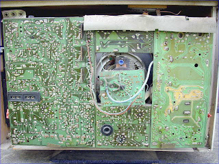
GALAXI DIGICOLOR 26" CHASSIS ITT(SEL) (453705 445101 455101) Automatic brightness control circuit :
A multiple automatic brightness control for a television receiver including a first automatic brightness limiter (ABL) circuit responsive only to relatively long duration changes in brightness-producing current and a second ABL circuit responsive to brightness-producing current changes of shorter duration than the first ABL circuit. Both ABL circuits have threshold levels below which they are not responsive to brightness-producing current changes, but the threshold level of the second ABL circuit is higher than that of the first so that, while the second ABL circuit responds more quickly than the first, it does so only for higher amplitude changes in the brightness-producing current.
 1. An automatic brightness limiter for a cathode ray tube, comprising:
A. a brightness current circuit through which flows a current proportional to the brightness of an image displayed on said cathode ray tube;
B. brightness control means responsive to control signals applied thereto for controlling the brightness of said displayed image;
C. a first automatic brightness limiter circuit coupled to said brightness current circuit to respond to brightness current in excess of a first threshold brightness current level for producing a first control signal to limit said brightness current to said first threshold level, said first automatic brightness limiter circuit comprising a first time constant circuit through which said first control signal is applied to said brightness control means;
D. a second automatic brightness limiter circuit coupled to said brightness current circuit to respond to brightness current only in excess of a second threshold brightness current level higher than said first threshold level for producing a second control signal to limit said brightness current to said second threshold level, said second automatic brightness limiter circuit comprising a second time constant circuit having a lower time constant value than said first time constant circuit and through which said second control signal is applied to said brightness control means such that said brightness control means is responsive to second control signal frequencies higher than the maximum frequency of said first control signal; and in which said brightness current circuit includes:
a. a source of said brightness current; and
b. a voltage divider connected to said source of brightness current, said first automatic brightness limiter circuit being connected to a first connection point on said divider and said second automatic brightness limiter circuit being connected to a second connection point on said divider, said second point being positive relative to said first point.
2. An automatic brightness limiter for a cathode ray tube, comprising:
A. a brightness current circuit through which flows a current proportional to the brightness of an image displayed on said cathode ray tube;
 B. a first automatic brightness limiter circuit coupled to said brightness current circuit to respond to brightness current in excess of a first threshold brightness current level and to limit said brightness current to said first threshold level, said first automatic brightness limiter circuit comprising a first time constant circuit to limit the maximum frequency to which said first automatic brightness limiter circuit can respond to a first value; and
C. a second automatic brightness limiter circuit coupled to said brightness current circuit to respond to brightness current only in excess of a second threshold brightness current level higher than said first threshold level to limit said brightness current to said second threshold level, said second automatic brightness limiter circuit comprising a second time constant circuit having a lower time constant value than said first time constant circuit to be responsive to frequencies higher than said maximum frequency of said first time constant circuit, and further comprising a transistor having an emitter connected to a connection point in said brightness current circuit, a base connected to a source of reference voltage, and a collector connected to a brightness-controlling terminal.
3. The invention as defined in claim 2 comprising, in addition, a luminance circuit comprising said brightness-controlling terminal. 4. An automatic brightness control circuit of a television receiver comprising:
A. a cathode ray tube comprising anode, grid, and cathode electrodes wherein video signals are applied to the cathode of said cathode ray tube;
B. a signal channel for applying video signals to the cathode ray tube to reproduce images thereon;
C. a high voltage circuit for applying a high voltage to the anode of said cathode ray tube to cause brightness current to flow between said anode and cathode electrodes;
D. brightness current detecting means connected to said high voltage circuit for detecting brightness current of said cathode ray tube;
E. a first control circuit connected to said current detecting means for limiting brightness of the images reproduced on said cathode ray tube, said first control circuit comprising a first time constant and being operable only when said brightness current exceeds a first threshold level, said first control circuit is connected to said signal channel for controlling the gain thereof; and
F. a second control circuit connected to said current detecting means for limiting brightness of the images reproduced on said cathode ray tube, said second control circuit comprising a second time constant and being operable only when said brightness current exceeds a second threshold level, said first time constant being greater than said second time constant, and said first threshold level being lower than said second threshold level, said second control circuit is connected to the grid of said cathode ray tube for controlling the voltage thereof.
5. An automatic brightness control circuit of a television receiver comprising:
A. a cathode ray tube comprising anode, grid, and cathode electrodes wherein video signals are applied to the cathode of said cathode ray tube;
B. a signal channel for applying video signals to the cathode ray tube to reproduce images thereon;
C. a high voltage circuit for applying a high voltage to the anode of said cathode ray tube to cause brightness current to flow between said anode and cathode electrodes;
D. brightness current detecting means connected to said high voltage circuit for detecting brightness current of said cathode ray tube;
E. a first control circuit connected to said current detecting means for limiting brightness of the images reproduced on said cathode ray tube, said first control circuit comprising a first time constant and being operable only when said brightness current exceeds a first threshold level;
F. a second control circuit connected to said current detecting means for limiting brightness of the images reproduced on said cathode ray tube, said second control circuit comprising a second time constant and being operable only when said brightness current exceeds a second threshold level, said first time constant being greater than said second time constant, and said first threshold level being lower than said second threshold level; and
both said first and second control circuits are connected to said signal channel for controlling the gain thereof.
6. An automatic brightness control circuit of a television receiver comprising:
A. a cathode ray tube comprising anode, grid, and cathode electrodes;
B. a signal channel for applying video signals to the cathode ray tube to reproduce images thereon;
C. a high voltage circuit for applying a high voltage to the anode of said cathode ray tube to cause brightness current to flow between said anode and cathode electrodes;
D. brightness current detecting means connected to said high voltage circuit for detecting brightness current of said cathode ray tube;
E. a first control circuit connected to said current detecting means for limiting brightness of the images reproduced on said cathode ray tube, said first control circuit comprising a first time constant and being operable only when said brightness current exceeds a first threshold level; and
F. a second control circuit connected to said current detecting means for limiting brightness of the images reproduced on said cathode ray tube, said second control circuit comprising a second time constant and being operable only when said brightness current exceeds a second threshold level, said first time constant being greater than said second time constant, and said first threshold level being lower than said second threshold level, in which said second control circuit comprises a switching transistor having a base connected to a source of reference voltage and an emitter connected to said current detecting means to cause said transistor to be conductive when said brightness current exceeds said second threshold level.
7. An automatic brightness control circuit of a television receiver comprising:
A. a cathode ray tube comprising anode, grid, and cathode electrodes;
B. a signal channel for applying video signals to the cathode ray tube to reproduce images thereon;
C. a high voltage circuit for applying a high voltage to the anode of said cathode ray tube to cause brightness current to flow between said anode and cathode electrodes;
D. brightness current detecting means connected to said high voltage circuit for detecting brightness current of said cathode ray tube;
E. a first control circuit connected to said current detecting means for limiting brightness of the images reproduced on said cathode ray tube, said first control circuit comprising a first time constant and being operable only when said brightness current exceeds a first threshold level; and
F. a second control circuit connected to said current detecting means for limiting brightness of the images reproduced on said cathode ray tube, said second control circuit comprising a second time constant and being operable only when said brightness current exceeds a second threshold level, said first time constant being greater than said second time constant, and said first threshold level being lower than said second threshold level, in which said second control circuit comprises: a neon tube coupled to said brightness current detecting means, and said second time constant being determined by said neon tube and capacitive means connected to said neon tube.
1. Field of the Invention
This invention relates to automatic brightness limiter (ABL) circuits and particularly to a combination of ABL circuits, one of which is responsive to brightness changes at a lower level than another but requiring the brightness changes to which it responds to last longer than the higher level changes to which the other ABL circuit responds.
2. The Prior Art
In a television receiver, it is desirable to limit the brightness of images produced on the screen of a cathode ray tube. The brightness is related to the anode current of the cathode ray tube, and this current must be produced by a high voltage power supply. The high voltage power supply may be damaged if it is required to supply too high a current for too long a time. Also, the high anode current may damage the fluorescent screen of the cathode ray tube. Whether or not there is any damage to the power supply or the cathode ray tube, excessively bright images may cause the viewers to feel eyestrain. In the form of sudden flashes that cause no other problem, they may simply be objectionable to the viewer.
The foregoing disadvantages of unnecessarily high brightness levels have been recognized in the past, and ABL circuits have been provided to control the brightness, especially in color television receivers. Since the brightness is proportional to the anode current of the cathode ray tube, such ABL circuits have usually been coupled to a circuit through which anode current of the cathode ray tube flows and have responded by controlling or limiting the luminance signal when the anode current rose above a threshold level.
It is desirable theoretically that an ABL circuit respond without delay, but actually such an ABL circuit is not possible. One reason it is not possible is that the anode current is not continuous but drops to zero during each horizontal and vertical blanking interval. Thus, even in the simplest form, the anode current may be considered to approximate a pulse wave. If the ABL circuit would be responsive to such rapid changes of anode current, or brightness, it could cause the quality of the reproduced television images to be deteriorated. Such deterioration could appear as blurred areas of darkness and light.
Therefore, it has been customary to design prior art ABL circuits to respond only to brightness levels so that only changes in brightness levels that are slower than the vertical scanning period are detected and accounted for. The time constant of an ABL circuit may have a value of 50 to 60 milli-seconds, which is about three or four times the duration of a vertical scanning period, so that the ABL circuit is not influenced by a change in brightness that lasts for only a single line scanning interval or less, or even by a change in brightness that lasts for a single vertical scanning interval. Such an ABL circuit is referred to as an averaging-type ABL circuit.
Averaging-type ABL circuits have several disadvantages. They cannot respond to rapid or momentary brightness changes, such as occur when the tuner, or channel selector, of a receiver is actuated to shift from one operating channel to another. When the tuner passes through unused frequency bands, the screen of the cathode ray tube may receive momentary flashes of high brightness. The period for passing through such unused frequency bands is usually short and is in the order of 20 milli-seconds, so that ABL circuits with time constants of 50 milli-seconds or more do not have time to respond. Other flashes of brightness too short to be controlled by averaging-type ABL circuits occur, for example, when the main power switch is actuated and when there are troubles in the driving circuits for the cathode ray tube.
It is an object of the present invention to provide an automatic brightness limiter circuit capable of responding quickly to limit sudden large brightness increases in an image display device and more slowly to limit brightness increases of lesser intensity.
It is another object of this invention to provide a novel automatic brightness control circuit in which first and second ABL circuits are utilized.
It is a further object of this invention to provide an improved ABL circuit which is responsive to a rapid or momentary change in brightness of images reproduced on the screen of a cathode ray tube.
Another object of the invention is to provide a combination of two automatic brightness limiter circuits coupled to a brightness current circuit, the first limiter circuit responding to brightness current in excess of a first threshold level and comprising a first time constant circuit to limit to a first value the maximum frequency to which the first limiter circuit can respond, and the second limiter circuit responding to brightness current only in excess of a higher threshold level than the first threshold level and comprising a second time constant circuit having a lower time constant value than the first time constant circuit to be responsive to frequencies higher than the maximum response frequency of the first time constant circuit.
SUMMARY OF THE INVENTION
The automatic brightness control circuit according to the present invention includes a first ABL circuit having a relatively long time constant value so that it responds to brightness current that exceeds the relatively low threshold value, provided the current remains in excess of that value for a long enough time. The control circuit also includes a second ABL circuit having a relatively short time constant so that it can respond to excess brightness signals more quickly than the first ABL circuit but having a higher threshold level than the first ABL circuits so that the brightness signals to which the second ABL circuit responds must be such as would produce higher brightness.
GALAXI DIGICOLOR 26" CHASSIS ITT(SEL) (453705 445101 455101) CHROMA-BURST SEPARATOR AND AMPLIFIER CIRCUIT :
A combined separator/amplifier for deriving chroma and burst signals comprises a differential amplifier having a pair of differentially acting transistors coupled to a common current source. The current source is formed by a transistor driven by unseparated chro ma and burst information from a composite color television signal. Bias networks force one differential transistor to be normally conductive and the other differential transistor to be normally nonconductive. An amplified chroma signal is available at the collector of the normally conductive transistor. During retrace, a single flyback pulse drives the differential transistors into their opposite conduction states, causing an amplified burst signal to be available at the collector of the normally nonconductive transistor. The circuit includes automatic chroma control and color killer action.
1. In a color television receiver for receiving a composite color television signal including a color reference burst signal and a chroma information signal, said burst signal and said chroma signal occurring at different points in time, a circuit for separating and amplifying both said burst signal and said chroma signal, comprising: 2. The circuit of claim 1 wherein said common means comprises a third amplifying means having a first electrode, a second electrode, and an output electrode, means coupling said output electrode of said third amplifying means to said commonly connected first electrodes of said first amplifying means and said second amplifying means, means coupling o
ne of said first and second electrodes of said third amplifying means to a reference potential, and means coupling the other of said first and second electrodes of said third amplifying means to a source of said burst signal and said chroma signal, whereby said common means forms a common current source for said first and second amplifying means. 3. The circuit of claim 2 including ACC means for developing a control signal for automatic chroma control of the color television receiver, and means coupling said control signal to said third amplifying means to control the current flow therethrough in proportion to said control signal. 4. The circuit of claim 2 wherein said first amplifying means and said second amplifying means each comprise a transistor having emitter, base, and collector electrodes corresponding to said first, second, and output electrodes, respectively, said common connecting means and said bias means causing said transistors to form a common emitter driven, differential operating amplifier. 5. The circuit of claim 4 wherein said third amplifying means comprises a transistor having emitter, base and collector electrodes corresponding to said first, second and output electrodes, respectively, whereby the collector electrode of said third amplifying means drives the emitter electrodes of said first and second amplifying means. 6. The circuit of claim 1 including a source of color killer signal generated when the color television receiver is receiving a black-and-white transmission, and said bias means includes means responsive to said color killer signal for biasing the differential amplifying means to cause said second amplifying means to be substantially nonconductive. 7. The circuit of claim 6 wherein said second amplifying means includes a semiconductor junction, and said color killer signal responsive means couples said color killer signal to the semiconductor junction with a polarity to back bias the semiconductor junction. 8. The circuit of claim 1 including deflection and high voltage means in said color television receiver for generating a flyback pulse occurring when said color reference burst signal is present, and said control means couples the flyback pulse to one of the first and second amplifying means to cause said differential amplifier to switch conduction states, said flyback pulse corresponding to said control signal. 9. The circuit of claim 8 wherein said first amplifying means includes a semiconductor junction, and said control means couples said flyback pulse to the semiconductor junction of said first amplifying means with a polarity to forward bias said semiconductor junction.
A. a brightness current circuit through which flows a current proportional to the brightness of an image displayed on said cathode ray tube;
B. brightness control means responsive to control signals applied thereto for controlling the brightness of said displayed image;
C. a first automatic brightness limiter circuit coupled to said brightness current circuit to respond to brightness current in excess of a first threshold brightness current level for producing a first control signal to limit said brightness current to said first threshold level, said first automatic brightness limiter circuit comprising a first time constant circuit through which said first control signal is applied to said brightness control means;
D. a second automatic brightness limiter circuit coupled to said brightness current circuit to respond to brightness current only in excess of a second threshold brightness current level higher than said first threshold level for producing a second control signal to limit said brightness current to said second threshold level, said second automatic brightness limiter circuit comprising a second time constant circuit having a lower time constant value than said first time constant circuit and through which said second control signal is applied to said brightness control means such that said brightness control means is responsive to second control signal frequencies higher than the maximum frequency of said first control signal; and in which said brightness current circuit includes:
a. a source of said brightness current; and
b. a voltage divider connected to said source of brightness current, said first automatic brightness limiter circuit being connected to a first connection point on said divider and said second automatic brightness limiter circuit being connected to a second connection point on said divider, said second point being positive relative to said first point.
2. An automatic brightness limiter for a cathode ray tube, comprising:
A. a brightness current circuit through which flows a current proportional to the brightness of an image displayed on said cathode ray tube;
B. a first automatic brightness limiter circuit coupled to said brightness current circuit to respond to brightness current in excess of a first threshold brightness current level and to limit said brightness current to said first threshold level, said first automatic brightness limiter circuit comprising a first time constant circuit to limit the maximum frequency to which said first automatic brightness limiter circuit can respond to a first value; andC. a second automatic brightness limiter circuit coupled to said brightness current circuit to respond to brightness current only in excess of a second threshold brightness current level higher than said first threshold level to limit said brightness current to said second threshold level, said second automatic brightness limiter circuit comprising a second time constant circuit having a lower time constant value than said first time constant circuit to be responsive to frequencies higher than said maximum frequency of said first time constant circuit, and further comprising a transistor having an emitter connected to a connection point in said brightness current circuit, a base connected to a source of reference voltage, and a collector connected to a brightness-controlling terminal.
3. The invention as defined in claim 2 comprising, in addition, a luminance circuit comprising said brightness-controlling terminal. 4. An automatic brightness control circuit of a television receiver comprising:
A. a cathode ray tube comprising anode, grid, and cathode electrodes wherein video signals are applied to the cathode of said cathode ray tube;
B. a signal channel for applying video signals to the cathode ray tube to reproduce images thereon;
C. a high voltage circuit for applying a high voltage to the anode of said cathode ray tube to cause brightness current to flow between said anode and cathode electrodes;
D. brightness current detecting means connected to said high voltage circuit for detecting brightness current of said cathode ray tube;
E. a first control circuit connected to said current detecting means for limiting brightness of the images reproduced on said cathode ray tube, said first control circuit comprising a first time constant and being operable only when said brightness current exceeds a first threshold level, said first control circuit is connected to said signal channel for controlling the gain thereof; and
F. a second control circuit connected to said current detecting means for limiting brightness of the images reproduced on said cathode ray tube, said second control circuit comprising a second time constant and being operable only when said brightness current exceeds a second threshold level, said first time constant being greater than said second time constant, and said first threshold level being lower than said second threshold level, said second control circuit is connected to the grid of said cathode ray tube for controlling the voltage thereof.
5. An automatic brightness control circuit of a television receiver comprising:
A. a cathode ray tube comprising anode, grid, and cathode electrodes wherein video signals are applied to the cathode of said cathode ray tube;
B. a signal channel for applying video signals to the cathode ray tube to reproduce images thereon;
C. a high voltage circuit for applying a high voltage to the anode of said cathode ray tube to cause brightness current to flow between said anode and cathode electrodes;
D. brightness current detecting means connected to said high voltage circuit for detecting brightness current of said cathode ray tube;
E. a first control circuit connected to said current detecting means for limiting brightness of the images reproduced on said cathode ray tube, said first control circuit comprising a first time constant and being operable only when said brightness current exceeds a first threshold level;
F. a second control circuit connected to said current detecting means for limiting brightness of the images reproduced on said cathode ray tube, said second control circuit comprising a second time constant and being operable only when said brightness current exceeds a second threshold level, said first time constant being greater than said second time constant, and said first threshold level being lower than said second threshold level; and
both said first and second control circuits are connected to said signal channel for controlling the gain thereof.
6. An automatic brightness control circuit of a television receiver comprising:
A. a cathode ray tube comprising anode, grid, and cathode electrodes;
B. a signal channel for applying video signals to the cathode ray tube to reproduce images thereon;
C. a high voltage circuit for applying a high voltage to the anode of said cathode ray tube to cause brightness current to flow between said anode and cathode electrodes;
D. brightness current detecting means connected to said high voltage circuit for detecting brightness current of said cathode ray tube;
E. a first control circuit connected to said current detecting means for limiting brightness of the images reproduced on said cathode ray tube, said first control circuit comprising a first time constant and being operable only when said brightness current exceeds a first threshold level; and
F. a second control circuit connected to said current detecting means for limiting brightness of the images reproduced on said cathode ray tube, said second control circuit comprising a second time constant and being operable only when said brightness current exceeds a second threshold level, said first time constant being greater than said second time constant, and said first threshold level being lower than said second threshold level, in which said second control circuit comprises a switching transistor having a base connected to a source of reference voltage and an emitter connected to said current detecting means to cause said transistor to be conductive when said brightness current exceeds said second threshold level.
7. An automatic brightness control circuit of a television receiver comprising:
A. a cathode ray tube comprising anode, grid, and cathode electrodes;
B. a signal channel for applying video signals to the cathode ray tube to reproduce images thereon;
C. a high voltage circuit for applying a high voltage to the anode of said cathode ray tube to cause brightness current to flow between said anode and cathode electrodes;
D. brightness current detecting means connected to said high voltage circuit for detecting brightness current of said cathode ray tube;
E. a first control circuit connected to said current detecting means for limiting brightness of the images reproduced on said cathode ray tube, said first control circuit comprising a first time constant and being operable only when said brightness current exceeds a first threshold level; and
F. a second control circuit connected to said current detecting means for limiting brightness of the images reproduced on said cathode ray tube, said second control circuit comprising a second time constant and being operable only when said brightness current exceeds a second threshold level, said first time constant being greater than said second time constant, and said first threshold level being lower than said second threshold level, in which said second control circuit comprises: a neon tube coupled to said brightness current detecting means, and said second time constant being determined by said neon tube and capacitive means connected to said neon tube.
Description:
BACKGROUND OF THE INVENTION1. Field of the Invention
2. The Prior Art
In a television receiver, it is desirable to limit the brightness of images produced on the screen of a cathode ray tube. The brightness is related to the anode current of the cathode ray tube, and this current must be produced by a high voltage power supply. The high voltage power supply may be damaged if it is required to supply too high a current for too long a time. Also, the high anode current may damage the fluorescent screen of the cathode ray tube. Whether or not there is any damage to the power supply or the cathode ray tube, excessively bright images may cause the viewers to feel eyestrain. In the form of sudden flashes that cause no other problem, they may simply be objectionable to the viewer.
The foregoing disadvantages of unnecessarily high brightness levels have been recognized in the past, and ABL circuits have been provided to control the brightness, especially in color television receivers. Since the brightness is proportional to the anode current of the cathode ray tube, such ABL circuits have usually been coupled to a circuit through which anode current of the cathode ray tube flows and have responded by controlling or limiting the luminance signal when the anode current rose above a threshold level.
It is desirable theoretically that an ABL circuit respond without delay, but actually such an ABL circuit is not possible. One reason it is not possible is that the anode current is not continuous but drops to zero during each horizontal and vertical blanking interval. Thus, even in the simplest form, the anode current may be considered to approximate a pulse wave. If the ABL circuit would be responsive to such rapid changes of anode current, or brightness, it could cause the quality of the reproduced television images to be deteriorated. Such deterioration could appear as blurred areas of darkness and light.
Therefore, it has been customary to design prior art ABL circuits to respond only to brightness levels so that only changes in brightness levels that are slower than the vertical scanning period are detected and accounted for. The time constant of an ABL circuit may have a value of 50 to 60 milli-seconds, which is about three or four times the duration of a vertical scanning period, so that the ABL circuit is not influenced by a change in brightness that lasts for only a single line scanning interval or less, or even by a change in brightness that lasts for a single vertical scanning interval. Such an ABL circuit is referred to as an averaging-type ABL circuit.
Averaging-type ABL circuits have several disadvantages. They cannot respond to rapid or momentary brightness changes, such as occur when the tuner, or channel selector, of a receiver is actuated to shift from one operating channel to another. When the tuner passes through unused frequency bands, the screen of the cathode ray tube may receive momentary flashes of high brightness. The period for passing through such unused frequency bands is usually short and is in the order of 20 milli-seconds, so that ABL circuits with time constants of 50 milli-seconds or more do not have time to respond. Other flashes of brightness too short to be controlled by averaging-type ABL circuits occur, for example, when the main power switch is actuated and when there are troubles in the driving circuits for the cathode ray tube.
It is an object of the present invention to provide an automatic brightness limiter circuit capable of responding quickly to limit sudden large brightness increases in an image display device and more slowly to limit brightness increases of lesser intensity.
It is another object of this invention to provide a novel automatic brightness control circuit in which first and second ABL circuits are utilized.It is a further object of this invention to provide an improved ABL circuit which is responsive to a rapid or momentary change in brightness of images reproduced on the screen of a cathode ray tube.
Another object of the invention is to provide a combination of two automatic brightness limiter circuits coupled to a brightness current circuit, the first limiter circuit responding to brightness current in excess of a first threshold level and comprising a first time constant circuit to limit to a first value the maximum frequency to which the first limiter circuit can respond, and the second limiter circuit responding to brightness current only in excess of a higher threshold level than the first threshold level and comprising a second time constant circuit having a lower time constant value than the first time constant circuit to be responsive to frequencies higher than the maximum response frequency of the first time constant circuit.
SUMMARY OF THE INVENTION
The automatic brightness control circuit according to the present invention includes a first ABL circuit having a relatively long time constant value so that it responds to brightness current that exceeds the relatively low threshold value, provided the current remains in excess of that value for a long enough time. The control circuit also includes a second ABL circuit having a relatively short time constant so that it can respond to excess brightness signals more quickly than the first ABL circuit but having a higher threshold level than the first ABL circuits so that the brightness signals to which the second ABL circuit responds must be such as would produce higher brightness.
GALAXI DIGICOLOR 26" CHASSIS ITT(SEL) (453705 445101 455101) CHROMA-BURST SEPARATOR AND AMPLIFIER CIRCUIT :
A combined separator/amplifier for deriving chroma and burst signals comprises a differential amplifier having a pair of differentially acting transistors coupled to a common current source. The current source is formed by a transistor driven by unseparated chro
 ma and burst information from a composite color television signal. Bias networks force one differential transistor to be normally conductive and the other differential transistor to be normally nonconductive. An amplified chroma signal is available at the collector of the normally conductive transistor. During retrace, a single flyback pulse drives the differential transistors into their opposite conduction states, causing an amplified burst signal to be available at the collector of the normally nonconductive transistor. The circuit includes automatic chroma control and color killer action.
 1. In a color television receiver for receiving a composite color television signal including a color reference burst signal and a chroma information signal, said burst signal and said chroma signal occurring at different points in time, a circuit for separating and amplifying both said burst signal and said chroma signal, comprising: 2. The circuit of claim 1 wherein said common means comprises a third amplifying means having a first electrode, a second electrode, and an output electrode, means coupling said output electrode of said third amplifying means to said commonly connected first electrodes of said first amplifying means and said second amplifying means, means coupling o
Description:
BACKGROUND OF THE INVENTION
This invention relates to a combined separator and amplifier circuit used in a color television receiver for deriving separate, amplified burst and chroma signals.
In a color television receiver, a separator and amplifier circuit is necessary to derive burst and chroma signals from a composite color television signal. Circuits are known which combine the function of a separator and an amplifier into a single stage. Typically, such circuits require a pair of flyback pulses to separately and alternately enable a burst channel and a chroma channel. For example, it has been known to drive a split-pentode vacuum tube with a pair of opposite going flyback pulses in order to alternately enable and disable chroma and burst channels connected to the pair of plates of the pentode.
Prior combined separator/amplifier circuits for deriving chroma and burst signals have a number of disadvantages. Some circuits require two flyback pulses of different polarity. Also such prior circuits have not been suitable for incorporation into linear integrated circuits. In addition, these circuits have been relatively complex, and not readily adapted for use with automatic chroma control and color killer action.
SUMMARY OF THE INVENTION
In accordance with the present invention, an improved separator/amplifier circuit uses a single differential amplifier to derive separate, amplified burst and chroma signals. Only a single flyback pulse is required to operate the circuit, and automatic chroma control and color killer action can easily be added with no increase in components or complexity. The circuit is readily adapted to linear integrated circuit techniques, and is of simple design and straightforward operation.
One object of this invention is to provide an improved chrominance and burst separating and amplifying circuit which operates as a differential amplifier.
Further objects and features of the invention will be apparent from the following description, and from the drawings.
BRIEF DESCRIPTION OF THE DRAWINGS
FIG. 1 is a block diagram of a color television receiver incorporating a novel chroma and burst separator and amplifier; and
FIG. 2 is a schematic diagram of the chroma and burst separator and amplifier shown in block form in FIG. 1.
DESCRIPTION OF THE PREFERRED EMBODIMENT
While an illustrative embodiment of the invention is shown in the drawings and will be described in detail herein, the invention is susceptible of embodiment in many different forms and it should be understood that the
present disclosure is to be considered as an exemplification of the principles of the invention and is not intended to limit the invention to the embodiment illustrated.
Turning to FIG. 1, a color television receiver is illustrated in which an incoming composite color television signal is received by an antenna 10 and coupled to conventional RF and IF amplifying stages 12. The amplified IF signal is coupled to a video detector 13 in order to reproduce the modulating video information which includes a luminance or Y signal, a chrominance or chroma signal modulated on a 3.58 megahertz carrier, and a 3.58 megahertz burst signal which is transmitted during the blanking interval for each scanning line.
A video amplifier 15 amplifies the luminance or Y signal and couples it to a tri-color cathode ray tube or CRT 17 through a delay line 18. A deflection and high voltage circuit 20, responsive to the output of video amplifier 15, derives the horizontal and vertical scanning signals for CRT 17. During the retrace time period, a flyback pulse for blanking the video display is generated from the horizontal output transformer in circuit 20, and appears on a line 21.
The chroma information signal modulated on the 3.58 megahertz carrier, and the 3.58 megahertz burst signal, is coupled through a chroma take-off circuit 22, such as a chroma bandpass filter, and via output line 23 to the applicant's novel combined chroma and burst separator/amplifier 25, shown in detail in FIG. 2. Circuit 25 provides, on a chroma output line 27, a separated and amplified chroma signal which is coupled to a color demodulator and matrix 30 in order to derive three color difference signals R-Y, B-Y, and G-Y for driving the CRT 17. Circuit 25 also has a burst output line 32 on which an amplified burst reference signal is coupled to a conventional injection locked oscillator 34 which generates oscillatory signals coupled to the color demodulator and matrix 30 for the purpose of demodulating the chroma signal.
The injection locked oscillator 34 also generates, during reception of a black-and-white transmission, a color killer signal which is coupled to a color killer amplifier 36. Amplifier 36 has an output line 37 which couples a color killer voltage to the circuit 25. In addition, oscillator 34 further generates an automatic chroma control or ACC voltage, on an output line 39, which is coupled to circuit 25. While the color killer and ACC signals have been illustrated as being derived from an injection locked oscillator, it will be appreciated that any conventional circuit may be used to derive these signals. By way of reference, a suitable injection locked oscillator which derives color killer and ACC voltages is shown in U.S. Pat. No. 2,982,812, issued May 2, 1961 to R. N. Rhodes et al.
In the block diagram of the color television receiver, certain additional circuits of known construction have not been illustrated, as they are not necessary for an understanding of the present invention. Other conventional arrangements for a color television receiver can be utilized, as desired. For example, the chroma take-off circuit 22 may include cascaded video amplifiers having an output directly coupled to the circuit 25. In such an event, the necessary bandpass filters would be added to the circuit 25, rather than being located in block 22.
In FIG. 2, the novel combined chroma and burst separator/amplifier circuit 25 is illustrated in detail. The circuit comprises a single differential amplifier having a pair of NPN transistors 50 and 51 coupled to a common current source formed by a third NPN transistor 52. The emitter electrodes of both transistors 50 and 51 are tied together and are in common with the collector electrode of transistor 52. The collector electrode of transistor 50 is coupled through a tuned tank consisting in parallel of an inductor 55, a capacitor 56, and a resistor 57 located between the collector electrode and a source of B+ voltage, such as 35 volts DC. The junction between the tank and the collector electrode of transistor 50 forms the burst output line 32. The collector electrode of transistor 51 is connected to a similar tuned tank consisting in parallel of an inductor 60, capacitor 61, a resistor 62 located between the collector electrode and the same source of B+. The chroma output line 27 is located between the tank and the collector electrode of transistor 51.
In order to bias the pair of transistors 50 and 51 in a differential or alternate manner, the base electrode of transistor 50 is connected through a coupling capacitor 67 to the flyback pulse line 21 which has, during retrace time, a positive going flyback pulse 69 thereon having a peak amplitude of 10 volts. The base electrode of transistor 50 is also coupled through a resistor 70 to a source of reference potential or ground 72. The base electrode of transistor 51 is coupled to ground 72 through the parallel combination of a resistor 75 and a capacitor 76. The base electrode is also directly coupled to the color killer amplifier output line 37.
Common current source transistor 52 has its emitter electrode coupled to ground 72 through a parallel resistor 80 and capacitor 81. The base electrode of transistor 52 is similarly shunted to ground 72 through a resistor 83, and is coupled to the chroma and burst input line 23 through a coupling capacitor 85. The ACC output line 39 is directly connected to the base electrode of transistor 52.
In operation, the bias voltages are selected to cause transistor 51 to be normally conductive and thereby amplify the chroma information signal. When the positive going flyback pulse 69 is applied to the base of transistor 50, it drives transistor 50 into conduction. Since transistors 50 and 51 operate as a differential pair, the conduction of transistor 50 drives transistor 51 to cut-off, thereby terminating the chroma output signal on the chroma output line 27. At the same time, the signal from the current source 52, which now consists of burst information, is amplified by the conducting transistor 50 and appears on the burst output line 32.
The differential amplifier including current source 52 is very suitable for incorporation into a linear integrated circuit. By using a simple differential amplifier, the burst is separated from the chroma, and both signals are separately amplified. In one embodiment which was constructed, the gain of the chroma channel including transistor 51 was approximately 13, and the gain of the burst channel including transistor 50 was approximately 16.
The gains of transistors 50 and 51, and therefore the resulting collector currents, can be varied by controlling the base bias of transistor 52. Therefore, automatic chroma control (ACC) can readily be provided by applying to the base of transistor 52, via ACC output line 39, a voltage proportional to the burst amplitude. Since the burst amplitude is also varied, a closed loop ACC circuit is formed.
Color killer action is provided by coupling a negative cut-off or back bias to the base-emitter semiconductor junction of transistor 51, in the absence of burst. Such a negative cut-off voltage is available on the killer output line 37 from the color killer amplifier.
If closed loop ACC was not desired, the connection of output line 39 to the base of transistor 52 can be replaced with a resistor (not illustrated) coupled to a B+ source. If the B+ source had a DC voltage of 35 volts, for example, then the replacement resistor could have a value of 12 kilohms, and the resistor 83 could have a value of 560 ohms. If color killer action was not desired, the output line 37 coupled to the base of transistor 51 can be replaced with a resistor (not illustrated) coupled to the same B+ source. Again, if the B+ source had a DC value of 35 volts, then the replacement resistor could have a value of 220 kilohms, and the resistor 75 could have a value of 33 kilohms. The last named resistors form a voltage divider which biastransistor 51 normally into conduction. This in turn drives transistor 50, in which resistor 70 could have a value of 33 kilohms, into nonconduction in the absence of a flyback pulse. When color killer and ACC are to be incorporated in the circuit 25, then the color killer amplifier and the source of the ACC signal, respectively, should be construed to provide the same biasing as described above.
Circuit 25 can be modified in various ways without departing from the present invention. For example, the circuit could be connected so that the flyback pulse was coupled to transistor 51 in order to drive it nonconductive, rather than the illustrated circuit in which the flyback pulse is coupled to transistor 50 in order to drive it conductive. Similarly, the flyback pulse can be coupled to either the base or emitter of transistors 50 and 51, with a polarity to either forward bias or reverse bias, respectively, the base-emitter semiconductor junction in each transistor 50 and 51. Other changes will be apparent to those skilled in the art.
This invention relates to a combined separator and amplifier circuit used in a color television receiver for deriving separate, amplified burst and chroma signals.
In a color television receiver, a separator and amplifier circuit is necessary to derive burst and chroma signals from a composite color television signal. Circuits are known which combine the function of a separator and an amplifier into a single stage. Typically, such circuits require a pair of flyback pulses to separately and alternately enable a burst channel and a chroma channel. For example, it has been known to drive a split-pentode vacuum tube with a pair of opposite going flyback pulses in order to alternately enable and disable chroma and burst channels connected to the pair of plates of the pentode.
Prior combined separator/amplifier circuits for deriving chroma and burst signals have a number of disadvantages. Some circuits require two flyback pulses of different polarity. Also such prior circuits have not been suitable for incorporation into linear integrated circuits. In addition, these circuits have been relatively complex, and not readily adapted for use with automatic chroma control and color killer action.
SUMMARY OF THE INVENTION
In accordance with the present invention, an improved separator/amplifier circuit uses a single differential amplifier to derive separate, amplified burst and chroma signals. Only a single flyback pulse is required to operate the circuit, and automatic chroma control and color killer action can easily be added with no increase in components or complexity. The circuit is readily adapted to linear integrated circuit techniques, and is of simple design and straightforward operation.
One object of this invention is to provide an improved chrominance and burst separating and amplifying circuit which operates as a differential amplifier.
Further objects and features of the invention will be apparent from the following description, and from the drawings.
BRIEF DESCRIPTION OF THE DRAWINGS
FIG. 1 is a block diagram of a color television receiver incorporating a novel chroma and burst separator and amplifier; and
FIG. 2 is a schematic diagram of the chroma and burst separator and amplifier shown in block form in FIG. 1.
DESCRIPTION OF THE PREFERRED EMBODIMENT
While an illustrative embodiment of the invention is shown in the drawings and will be described in detail herein, the invention is susceptible of embodiment in many different forms and it should be understood that the
Turning to FIG. 1, a color television receiver is illustrated in which an incoming composite color television signal is received by an antenna 10 and coupled to conventional RF and IF amplifying stages 12. The amplified IF signal is coupled to a video detector 13 in order to reproduce the modulating video information which includes a luminance or Y signal, a chrominance or chroma signal modulated on a 3.58 megahertz carrier, and a 3.58 megahertz burst signal which is transmitted during the blanking interval for each scanning line.
A video amplifier 15 amplifies the luminance or Y signal and couples it to a tri-color cathode ray tube or CRT 17 through a delay line 18. A deflection and high voltage circuit 20, responsive to the output of video amplifier 15, derives the horizontal and vertical scanning signals for CRT 17. During the retrace time period, a flyback pulse for blanking the video display is generated from the horizontal output transformer in circuit 20, and appears on a line 21.
The chroma information signal modulated on the 3.58 megahertz carrier, and the 3.58 megahertz burst signal, is coupled through a chroma take-off circuit 22, such as a chroma bandpass filter, and via output line 23 to the applicant's novel combined chroma and burst separator/amplifier 25, shown in detail in FIG. 2. Circuit 25 provides, on a chroma output line 27, a separated and amplified chroma signal which is coupled to a color demodulator and matrix 30 in order to derive three color difference signals R-Y, B-Y, and G-Y for driving the CRT 17. Circuit 25 also has a burst output line 32 on which an amplified burst reference signal is coupled to a conventional injection locked oscillator 34 which generates oscillatory signals coupled to the color demodulator and matrix 30 for the purpose of demodulating the chroma signal.
The injection locked oscillator 34 also generates, during reception of a black-and-white transmission, a color killer signal which is coupled to a color killer amplifier 36. Amplifier 36 has an output line 37 which couples a color killer voltage to the circuit 25. In addition, oscillator 34 further generates an automatic chroma control or ACC voltage, on an output line 39, which is coupled to circuit 25. While the color killer and ACC signals have been illustrated as being derived from an injection locked oscillator, it will be appreciated that any c
onventional circuit may be used to derive these signals. By way of reference, a suitable injection locked oscillator which derives color killer and ACC voltages is shown in U.S. Pat. No. 2,982,812, issued May 2, 1961 to R. N. Rhodes et al.In the block diagram of the color television receiver, certain additional circuits of known construction have not been illustrated, as they are not necessary for an understanding of the present invention. Other conventional arrangements for a color television receiver can be utilized, as desired. For example, the chroma take-off circuit 22 may include cascaded video amplifiers having an output directly coupled to the circuit 25. In such an event, the necessary bandpass filters would be added to the circuit 25, rather than being located in block 22.
In FIG. 2, the novel combined chroma and burst separator/amplifier circuit 25 is illustrated in detail. The circuit comprises a single differential amplifier having a pair of NPN transistors 50 and 51 coupled to a common current source formed by a third NPN transistor 52. The emitter electrodes of both transistors 50 and 51 are tied together and are in common with the collector electrode of transistor 52. The collector electrode of transistor 50 is coupled through a tuned tank consisting in parallel of an inductor 55, a capacitor 56, and a resistor 57 located between the collector electrode and a source of B+ voltage, such as 35 volts DC. The junction between the tank and the collector electrode of transistor 50 forms the burst output line 32. The collector electrode of transistor 51 is connected to a similar tuned tank consisting in parallel of an inductor 60, capacitor 61, a resistor 62 located between the collector electrode and the same source of B+. The chroma output line 27 is located between the tank and the collector electrode of transistor 51.
In order to bias the pair of transistors 50 and 51 in a differential or alternate manner, the base electrode of transistor 50 is connected through
a coupling capacitor 67 to the flyback pulse line 21 which has, during retrace time, a positive going flyback pulse 69 thereon having a peak amplitude of 10 volts. The base electrode of transistor 50 is also coupled through a resistor 70 to a source of reference potential or ground 72. The base electrode of transistor 51 is coupled to ground 72 through the parallel combination of a resistor 75 and a capacitor 76. The base electrode is also directly coupled to the color killer amplifier output line 37.Common current source transistor 52 has its emitter electrode coupled to ground 72 through a parallel resistor 80 and capacitor 81. The base electrode of transistor 52 is similarly shunted to ground 72 through a resistor 83, and is coupled to the chroma and burst input line 23 through a coupling capacitor 85. The ACC output line 39 is directly connected to the base electrode of transistor 52.
In operation, the bias voltages are selected to cause transistor 51 to be normally conductive and thereby amplify the chroma information signal. When the positive going flyback pulse 69 is applied to the base of transistor 50, it drives transistor 50 into conduction. Since transistors 50 and 51 operate as a differential pair, the conduction of transistor 50 drives transistor 51 to cut-off, thereby terminating the chroma output signal on the chroma output line 27. At the same time, the signal from the current source 52, which now consists of burst information, is amplified by the conducting transistor 50 and appears on the burst output line 32.
The differential amplifier including current source 52 is very suitable for incorporation into a linear integrated circuit. By using a simple differential amplifier, the burst is separated from the chroma, and both signals are separately amplified. In one embodiment which was constructed, the gain of the chroma channel including transistor 51 was approximately 13, and the gain of the burst channel including transistor 50 was approximately 16.
The gains of transistors 50 and 51, and therefore the resulting collector currents, can be varied by controlling the base bias of transistor 52. Therefore, automatic chroma control (ACC) can readily be provided by applying to the base of transistor 52, via ACC output line 39, a voltage proportional to the burst amplitude. Since the burst amplitude is also varied, a closed loop ACC circuit is formed.
Color killer action is provided by coupling a negative cut-off or back bias to the base-emitter semiconductor junction of transistor 51, in the absence of burst. Such a negative cut-off voltage is available on the killer output line 37 from the color killer amplifier.
If closed loop ACC was not desired, the connection of output line 39 to the base of transistor 52 can be replaced with a resistor (not illustrated) coupled to a B+ source. If the B+ source had a DC voltage of 35 volts, for example, then the replacement resistor could have a value of 12 kilohms, and the resistor 83 could have a value of 560 ohms. If color killer action was not desired, the output line 37 coupled to the base of transistor 51 can be replaced with a resistor (not illustrated) coupled to the same B+ source. Again, if the B+ source had a DC value of 35 volts, then the replacement resistor could have a value of 220 kilohms, and the resistor 75 could have a value of 33 kilohms. The last named resistors form a voltage divider which bias
transistor 51 normally into conduction. This in turn drives transistor 50, in which resistor 70 could have a value of 33 kilohms, into nonconduction in the absence of a flyback pulse. When color killer and ACC are to be incorporated in the circuit 25, then the color killer amplifier and the source of the ACC signal, respectively, should be construed to provide the same biasing as described above.Circuit 25 can be modified in various ways without departing from the present invention. For example, the circuit could be connected so that the flyback pulse was coupled to transistor 51 in order to drive it nonconductive, rather than the illustrated circuit in which the flyback pulse is coupled to transistor 50 in order to drive it conductive. Similarly, the flyback pulse can be coupled to either the base or emitter of transistors 50 and 51, with a polarity to either forward bias or reverse bias, respectively, the base-emitter semiconductor junction in each transistor 50 and 51. Other changes will be apparent to those skilled in the art.
GALAXI DIGICOLOR 26" CHASSIS ITT(SEL) (453705 445101 455101) PAL-TYPE COLOR SIGNAL PROCESSING:
Burst components of PAL-type encoded signal are retained with modulated subcarrier components as they are processed in 1H delay line assembly and delivered to respective demodulators. Reference oscillation phase to which R-Y demodulator responds is effectively reversed every other line, in response to PAL switch apparatus, in order to provide desired R-Y output in successive lines. Reference oscillation phase to which B-Y demodulator responds is alternated by quadrature switch apparatus between B-Y phase (applied throughout each line interval) and R-Y phase (applied during each inter-line blanking interval). A first gating circuit, coupled to the output of the B-Y demodulator, selects that portion of the B-Y demodulator output developed during the burst interval for passage to integrating and amplifying means in order to develop an AFPC voltage for phase control of the local reference oscillator. A second gating circuit, coupled to the output of the R-Y demodulator, selects that portion of the R-Y demodulator output developed during the burst interval for passage to ACC and color killer circuitry. During color operation (enabled state of bandpass chrominance amplifier) the ACC circuiry develops a control current from the second gating circuit output that adjusts the chrominance amplifier gain in a direction appropriate to maintaining burst amplitude substantially constant at a level set by a manual chroma control. The color killer enables the chrominance amplifier for color operation only when the gated R-Y output indicates by its amplitude the presence of a burst in the received signal and by its polarity the correct switching mode for the PAL switch. Unless such circumstances are present, the color killer disables the chrominance amplifier during each line interval; the killer is keyed, however, to enable the chrominance amplifier during each burst interval so that recovery from the disable state may be effected when appropriate. The color killer circuitry also passes a reset pulse to the PAL switch in the absence of a correct mode indication in the gated R-Y output. The color killer circuitry further serves to control the effectiveness of a subcarrier trap for the receiver's luminance channel, removing the trap during line intervals of monochrome operation.
1. In apparatus for processing PAL-type encoded color television signals, the combination comprising: 2. Apparatus in accordance with claim 1, also including: 3. Apparatus in accordance with claim 2, also including: 4. Apparatus in accordance with claim 2, also including 5. Apparatus in accordance with claim 2, wherein said second reference oscillation supplying means includes means for reversing the phase of the supplied reference oscillation in alternate line intervals, and wherein said apparatus also includes: 6. Apparatus in accordance with claim 5, also including a source of line rate triggering pulses; and 7. Apparatus in accordance with claim 6, also including:
1. In apparatus for processing PAL-type encoded color television signals, the combination comprising: 2. Apparatus in accordance with claim 1, also including: 3. Apparatus in accordance with claim 2, also including: 4. Apparatus in accordance with claim 2, also including 5. Apparatus in accordance with claim 2, wherein said second reference oscillation supplying means includes means for reversing the phase of the supplied reference oscillation in alternate line intervals, and wherein said apparatus also includes: 6. Apparatus in accordance with claim 5, also including a source of line rate triggering pulses; and 7. Apparatus in accordance with claim 6, also including:
Description:
This invention relates generally to color television signal processing systems, and, particularly, to novel and improved systems for processing color television signals of the PAL type.
 In a color television receiver responding to a PAL transmission, the video signal output of the receiver's video detector includes, in addition to a wideband luminance component, a chrominance component in the form of a modulated subcarrier, and representing the summation of (a) the sideband products of the modulation of a subcarrier wave of fixed frequency and a first given phase by blue color-difference (B-Y) signals, and (b) the sideband products of the modulation of a subcarrier wave of the same fixed frequency, but with a quadrature phase relation to the first given phase, by red color difference (R-Y) signals, the second phase, however, being shifted by 180° in successive line intervals. The video signal, moreover, includes a color synchronizing burst component occurring during the inter-line blanking interval, incorporated in the transmission with a fixed amplitude and fixed (subcarrier) frequency, but alternating in phase in successive blanking intervals ±45° about a -(B-Y) phase (thereby corresponding to the summation of a fixed amplitude, constant-phase -(B-Y) burst component and a line-by-line phase reversing R-Y burst component of comparable fixed amplitude).
In a widely used approach to the processing of such detector PAL signals, the following functions are performed: A bandpass chrominance channel provides frequency selective amplification of the subcarrier sideband components, to the exclusion of low frequency luminance signals. The selectively amplified signals are applied to a 1H delay line assembly to develop two outputs respectively corresponding to an additive combination of undelayed and delayed signals, and a subtractive combination of undelayed and delayed signals. One output (in which the B-Y components for successive line intervals reinforce, whereas the R-Y components for successive line intervals mutually cancel) is supplied to a B-Y demodulator, while the other output (in which the R-Y components for successive line intervals reinforce, whereas the B-Y components for successive line intervals mutually cancel) is supplied to a R-Y demodulator. Each demodulator functions as a synchronous detector, controlled by the application of the appropriate phase of subcarrier frequency oscillations of fixed amplitude from a local reference oscillator. The reference phase applied to the B-Y demodulator is constant line-to-line, whereas the reference phase applied to the R-Y demodulator is shifted by 180° in successive line intervals. A takeoff for the burst component of the received signal is provided at a point in the chrominance channel prior to the delay line assembly, with appropriately gated apparatus extracting the burst component alone for amplification and delivery to a phase detector for comparison with an output of the local reference oscillator. An AFPC control voltage derived from the phase detector serves to lock the oscillator in a fixed phase relationship to the average phase of the "swinging" burst. Information derived from the separated burst is also used in performance of color killer and automatic chroma control (ACC) functions (determining the enabling or disabling of the chrominace channel, and the relative gain thereof when enabled). The burst component is eliminated from the chrominance signal delivered to the delay line assembly.
 In accordance with the principles of the present invention, novel approaches to PAL color signal processing are contemplated which depart, in many regards, from the above-described widely used approach. Pursuant to the principles of the present invention, burst separation prior to delay is not effected, a separate burst amplifying channel and separate AFPC phase detector are not employed, and burst suppression is not effected for the signal delivered to the 1H delay line assembly. Rather, the burst is retained in the signal delivered to the 1H delay line assembly, and the respective B-Y and R-Y components of the burst pass to the respective demodulators. The B-Y demodulator then serves a dual function: as the B-Y demodulator during line intervals, and as an AFPC Phase detector during interline burst intervals. The phase of reference oscillations supplied to the B-Y demodulator is switched from its normal B-Y phase to an R-Y phase between line intervals, so that the polarity of the demodulator output during a burst interval is indicative of the direction of departure from correct phase relationship between local oscillator and incoming signal. A gating circuit, coupled to the output of the B-Y demodulator, selects that portion of the B-Y demodulator output developed during the burst interval for passage to an integrating and amplifying means in order to develop an AFPC voltage to control the local reference oscillator.
In accordance with further aspects of the present invention, the R-Y demodulator also serves a dual function: as the R-Y demodulator during line intervals, and as a synchronous in-phase detector of burst amplitude during the inter-line burst intervals. A second gating circuit, coupled to the output of the R-Y demodulator, selects that portion of the R-Y demodulator output developed during the burst interval for passage to automatic chroma control (ACC) and color killer circuitry. During color operation (enabled state of bandpass chrominance amplifier) the ACC circuitry develops a control current from the second gating circuit output that adjusts the chrominance amplifier gain in a direction appropriate to maintaining burst amplitude substantially constant at a level set by a manual chroma control. The color killer enables the chrominance amplifier for color operation only when the gated R-Y output indicates by its amplitude the presence of a burst in the received signal and by its polarity the correct switching mode for the PAL switch (i.e., for the reference phase reversing switch associated with the R-Y demodulator). Unless such circumstances are present, the color killer disables the chrominance amplifier during each line interval; the killer is keyed, however, to enable the chrominance amplifier during each inter-line interval so that recovery from the disabled state may be effected when appropriate.
In accordance with still further aspects of the present invention, the color killer circuitry may serve several additional functions, viz.: (a) passing a reset pulse to the PAL switch apparatus, in the absence of a correct mode indication in the gated R-Y output (so that PAL switching mode synchronization may be realized; and (b) controlling the effectiveness of a subcarrier trap for the receiver's luminance channel, removing the trap during line intervals of monochrome operation.
An object of the present invention is to provide novel and improved signal processing apparatus for PAL-type color television signals.
Other objects and advantages of the present invention will be readily apparent to those skilled in the art upon a reading of the following detailed description and an inspection of the accompanying drawings in which:
FIG. 1 is a block diagram illustration of a portion of a color television receiver incorporating color signal processing apparatus embodying the principles of the present invention;
FIG. 2 depicts schematically illustrative apparatus for performing the AFPC function in the system of FIG. 1;
FIG. 3 depicts schematically illustrative apparatus for performing the ACC function in the system of FIG. 1; and
FIG. 4 depicts schematically illustrative apparatus for performing the color killer (and associated PAL switch resetting, and color subcarrier trap switching) functions in the system of FIG. 1.
I n FIG. 1, a portion of a PAL color television receiver, incorporating an embodiment of the present invention, is illustrated. The video detector 11 recovers a PAL encoded signal from the output of the receiver's intermediate frequency amplifier (not illustrated). The detector output is applied to a video amplifier 15 via a manual contrast control 13, which is bypassed by a burst circuit 14.
The manual contrast control 13 provides a facility for adjustment of the peak-to-peak magnitude of the video signals delivered to amplifier 15; however, the bypass circuit 14 permits the color synchronizing burst component to pass to amplifier 15 without being affected by contrast control adjustment. This arrangement ensures that contrast control adjustment does not introduce an undesired change in saturation of the image colors; i.e., the contrast control provides concomitant adjustments of the luminance and chrominance components, but does not disturb the burst component amplitude (to which subsequent ACC circuitry is responsive).
The output of video amplifier 15 is applied to a wideband luminance channel, including a luminance amplifier (not illustrated), and also, via chroma takeoff circuitry 17, to a chrominance channel, including a gain controlled bandpass amplifier 19. The chroma takeoff circuitry 17 provides a frequency selective input for the chrominance channel, passing the color subcarrier sideband components, to the substantial exclusion of low frequency luminance components; the chroma takeoff circuitry 17 also functions as a subcarrier trap for the luminance channel, significantly reducing the response of the luminance channel to signal frequencies in the vicinity of the color subcarrier. Desirably, the effectiveness of the trapping function is controlled as a function of whether the signal received is a monochrome or color transmission, with trapping eliminated in the former instance; the manner in which such trapping control is effected with be subsequently described.
The output of bandpass amplifier 19 is supplied to a 1H delay line assembly 21, which provides a pair of outputs representing additive and subtractive combinations of delayed and undelayed signals. At output terminal U of the delay line assembly 21, a combination is provided in which the B-Y components of succesive lines reinforce, whereas the shifting R-Y components tend to cancel; this output is supplied to an input terminal (35) of a B-Y demodulator 30. At a second output terminal (V) of the delay line assembly 21, a signal combination is provided in which the R-Y components of successive lines reinforce, whereas the B-Y components tend to cancel; this output is supplied to an input terminal (45) of an R-Y demodulator 40.
Each of the demodulators 30 and 40 function as a synchronous detector, heterodyning the respective delay line assembly output with unmodulated reference oscillations, of subcarrier frequency and respectively appropriate phase. Illustratively, each demodulator is of a type having (1) a pair of output terminals at which appear respective opposite polarity versions of the color-difference signal product of demodulation, and (2) a pair of reference oscillation input terminals with opposing effects on the polarity of the demodulator outputs.
The source of reference oscillations for the demodulators is reference oscillator 65, operating at the subcarrier frequency (e.g., 4.43 MHz.) and subject to phase control in a manner to be described. An output of oscillator 65 is applied to a quadrature switch 67, controlled by a horizontal blanking pulse input, the switch serving to alternately deliver (a) reference oscillations in a B-Y phase (during each line interval to reference input terminal 31 of demodulator 30, and (b) reference oscillations in a R-Y phase (during each inter-line blanking interval) to reference input terminal 33 of demodulator 30.
The B-Y component output of delay line assembly 21 is thus subject to in-phase synchronous detection during each line interval to a provide a B-Y color-difference signal output at terminal 37, and a -(B-Y) color-difference signal output at terminal 39.
At this point, it is appropriate to note that the color synchronizing burst portion of the video signal amplified in video amplifier 15 has been retained with the line interval subcarrier sideband components throughout the chrominance channel (17, 19, 21). The constant phase -(B-Y) component of the swinging burst thus appears in the signal output at delay line assembly terminal U. This component, accordingly, is subject to quadrature synchronous detection in demodulator 30, in view of the delivery by quadrature switch 67 of reference oscillations in the R-Y phase to the (inverting) reference input terminal 33.
B-Y demodulator 30 thereby conveniently serves as the equivalent of the burst phase detector employed in the usual AFPC arrangement. A B-Y burst interval gate 61, activated by an appropriately timed burst gate pulse, is coupled to output terminal 37, and serves to pass the portion of the demodulator output developed during the burst interval, i.e., the result of phase detection of the -(B-Y) burst component, to an AFPC amplifier 63. An integrated and amplified version of the gated output, with amplitude and polarity respectively indicative of degree and direction of departure from correct phase relationship between oscillator and received signal, is supplied by amplifier 63 to a suitable phase control element of oscillator
Reference oscillations in the R-Y phase are delivered in a linewise alternating fashion from the PAL switch apparatus 69, controlled by a horizontal blanking pulse input, to the respective reference input terminals (noninverting terminal 41 and inverting terminal 43) of R-Y demodulator 40. If the switching mode of the PAL switch 69 is the correct one, the alternating polarity line interval R-Y component at terminal V of delay line assembly 21 will be subject to in-phase detection by demodulator 40 in the desired fashion, developing a R-Y color-difference signal at output terminal 47, and a -(R-Y) color-difference signal at output terminal 49. The latter output signal is supplied, along with the -(B-Y) output of demodulator 30, to a matrix circuit 50, for development of a third (G-Y) color-difference signal.
An R-Y burst component also appears in the signal input to terminal 45 of the R-Y demodulator 40, and is subject to in-phase synchronous detection when the correct switching mode is in effect. An R-Y burst interval gate 71, coupled to output terminal 47 of demodulator 40, is gated by a suitably timed burst gate pulse to pass that portion of the R-Y demodulator output developed during the burst interval to a pair of circuits (ACC amplifier circuit 73 and keyed color killer circuit 77).
The ACC (automatic chroma control) circuitry 73 functions to integrate and amplify the gated R-Y demodulator output in order to develop a control current for controlling the gain of bandpass amplifier 19. The gain control is effected in a direction to oppose spurious variations in the amplitude of the R-Y burst component (which is transmitted with fixed amplitude), thereby to minimize spurious variations in the chrominance signal amplitude that may result in incorrect saturation (chroma) of the displayed image colors. A facility for manual adjustment of the saturation of the image colors is provided in the form of a manual chroma control 75, which supplies an adjustable reference potential to ACC amplifier 73 for comparison with the gated R-Y demodulator output from gate 71 to determine the control current magnitude.
The keyed color killer circuit 77 controls the enabling and disabling of the bandpass amplifier 19, responding to the amplitude and polarity of the gated R-Y demodulator output from gate 71. The amplifier 19 is enabled, permitting amplification thereby of the line interval subcarrier sideband components, when the gate 71 output amplitude indicates presence of a color transmission with a burst of adequate amplitude for synchronization, and when gate 71 output polarity indicates operation of the PAL switch in the correct switching mode. In the absence of such circumstances, the color killer circuit 77 holds the amplifier in a disabled state; the color killer circuit is, however, keyed in response to a horizontal blanking pulse input in a manner enabling operation of the amplifier 19 during the burst interval to ensure the ability of the system to recover from the disabled state when appropriate. Alteration of the PAL switch operation to a correct mode is also facilitated by the keyed color killer circuit 77, which permits passage of a reset pulse to the PAL switch apparatus, when circuit 77 holds amplifier 19 in a disabled state.
The keyed color killer circuit 77 also serves the previously mentioned trap switching function, causing circuit 17 to be effective as a subcarrier trap for the luminance channel when amplifier 19 is enabled, and to be ineffective as a subcarrier trap when amplifier 19 is disabled.
FIG. 2 provides, in schematic detail, an illustration of particular circuit arrangements that may advantageously be employed for portions of th e FIG. 1 system (and in particular, those portions associated with oscillator synchronization: B-Y demodulator 30, B-Y burst interval gate 61, AFPC amplifier 63, reference oscillator 65, and quadrature switch 67).
The B-Y demodulator 30 in FIG. 2 employs six transistors (301, 302, 303, 304, 305 and 306 conveniently realized in integrated form on a common monolithic integrated circuit chip 300) arranged in a cross-coupled differential amplifier pair configuration. In the circuit arrangement, the emitters of transistors 301 and 302 are joined directly and returned to a bias supply (e.g., - 15 volts) via the collector-emitter path of transistor 303 and emitter resistor 310; likewise, the emitters of transistors 304 and 305 are joined directly and returned to the bias supply via the collector-emitter path of transistor 306 and the common emitter resistor 310.
The base of transistor 301 serves as the non-inverting reference input terminal 31 of the demodulator; the base (terminal 31') of transistor 304 is directly linked thereto. The base of transistor 302 serves as the inverting reference input terminal 33 of the demodulator the base (terminal 33') of transistor 305 is directly linked thereto. The collector of transistor 301 serves as the B-Y color-difference signal output terminal 37 of the demodulator; the collector (terminal 37') of transistor 305 is directly linked thereto. The collector of transistor 302 serves as the -(B-Y) color-difference signal output terminal 39 of the demodulator; the collector (terminal 39') of transistor 304 is directly linked thereto.
The base of transistor 303 serves as the modulated subcarrier input terminal 35 of the demodulator, receiving the signals appearing at terminal U of the delay line assembly 21 (FIG. 1). The base of transistor 306 is effectively held at AC ground potential by suitable bypassing.
The signal output appearing at terminal 37, free of subcarrier frequency components due to cancellation effects from the contributing transistors (301, 305), is applied to emitter follower transistor 307. A B-Y color-difference signal output is available at the emitter of transistor 307 for combination with a luminance component in the matrix and display portion of the receiver (not illustrated).
The emitter of transistor 307 is also linked by a path including resistor 613 and capacitor 614 to the junction (J) of oppositely poled electrodes of a pair of diodes 611 and 612. The collector-emitter path of a gate transistor 610 short circuits junction J to ground throughout each line interval. During each burst interval, however, the short circuit is removed, as transistor 610 is cut off by the positive-going pulse portion b of a gating waveform applied to its base. The cutoff of transistor 610 during each burst interval permits conduction by one of the diodes (611 or 612, depending upon the polarity of the burst interval output of demodulator 30) to charge the respectively associated capacitor (615 or 616) to a level dependent upon the magnitude of the burst interval output of demodulator 30. Transistor 610 and associated circuitry thus performs the function of the B-Y burst interval gate 61 of the FIG. 1 system.
AFPC amplifier 63 includes a pair of transistors 631 and 633 disposed in a differential amplifier configuration, with the base of input transistor 631 coupled to respond to the potential across the charged capacitor (615 or 616). The integrated output of amplifier 63 appears across capacitor 635, coupled between the collector of output transistor 633 and ground.
Reference oscillator 65 employs a transistor 651 associated with reactive circuit elements in a Colpitts configuration, with the inductive circuit branch including a frequency determining crystal 653 in series with a variable capacitance diode 652. A resistor links the collector of AFPC amplifier output transistor 633 to the junction of crystal 653 and diode 652, whereby the reverse bias on diode (and hence its capacitance) is subject to variation in accordance with the integrated output of amplifier 63 in order to effect the desired frequency and phase synchronization.
The output of reference oscillator 65 is derived from the collector of transistor 651 and applied via an emitter follower transistor 655 to a reference oscillation feed point R. Quadrature switch apparatus 67 controls the application of reference oscillations from feed point R to respective reference input terminals of the B-Y demodulator 30.
Quadrature switch 67 employs a pair of switching transistors 675 and 676. Switching transistor 676 is normally conducting, but is cut off during each inter-line blanking interval by the neagive-going pulse portion n of a gating waveform applied to its base. In complementary fashion, switching transistor 675 is rendered conducting only during the inter-line blanking interval by the positive going pulse portion p of a gating waveform applied to its base.
The collector-emitter path of switching transistor 676 is connected between the demodulator reference input terminal 33 and ground, while the collector-emitter path of switching transistor 675 is connected between the demodulator reference input terminal 31 and ground. A resistor 674 links feed point R to reference input terminal 33. A resistor 671 in series with a coil 672 links feed point R to reference input terminal 31. A capacitor 673 is connected between reference input terminal 31 and ground, and is adjusted for series resonance with coil 672 at the reference oscillation frequency.
during each line interval, the conduction of switching transistor 676 short circuits reference input terminal 33 to ground, precluding the feeding of reference oscillations to that terminal. Switching transistor 675, however, is nonconducting each line interval, permitting the feeding of reference oscillations to terminal 31. Circuit elements 672 and 673 introduce a phase shift of 90° from the R-Y phase to which the oscillator output is held, so that the reference oscillations delivered during line intervals are at the B-Y phase.
During each inter-line blanking interval, the conduction of switching transistor 675 short circuits reference input terminal 31 to ground, precluding the feeding of reference oscillations to that terminal. Switching transistor 676, however, is nonconducting during each inter-line blanking interval, permitting the feeding of reference oscillations to terminal 33 in the R-Y phase.
F IG. 3 provides, in schematic detail, an illustration of particular circuit arrangements that may advantageously be employed for additional portions of the FIG. 1 system (particularly, those portions associated with automatic chroma control: R-Y demodulator 40, R-Y burst interval gate 71, ACC amplifier 73, manual chroma control 75, video amlifier 15, chroma takeoff 17, and bandpass amplifier 19).
The R-Y demodulator 40 employs six transistors (401, 402, 403, 404, 405 and 406) disposed on a monolithic integrated circuit chip 400, and arranged in a cross-coupled differential amplifier configuration identical to that previously explained for the B-Y demodulator 30.
 The base of transistor 401 serves as the non-inverting reference input terminal 41 of the demodulator, the base (terminal 41') of transistor 404 is directly linked thereto. The base of transistor 402 serves as the inverting reference input terminal 43 of the demodulator; the base (terminal 43') of transistor 405 is directly linked thereto. The collector of transistor 401 serves as the R-Y color-difference signal output terminal 47 of the demodulator; the collector (terminal 47') of transistor 405 is directly linked thereto. The collector of transistor 402 serves as the -(B-Y) color-difference signal output terminal 49 of the demodulator; the collector (terminal 49') of transistor 404 is directly linked thereto.
The base of transistor 403 serves as the modulated subcarrier input terminal 45 of the demodulator, receiving the signals appearing at terminal V of delay line assembly 21 (FIG. 1). The base of transistor 406 is effectively held at AC ground potential by suitable bypassing.
The signal output appearing at terminal 47, free of subcarrier frequency components, is applied to emitter follower transistor 407. An R-Y color-difference signal output is derived from the emitter of transistor 407. A path, including, in series, a resistor 713, capacitor 714 and resistor 715 is also provided between the emitter of transistor 407 and the base of an additional emitter follower transistor 711. The emitter-collector path of a gating transistor 710 is connected between ground and the junction of capacitor 714 and resistor 715; the junction is short circuited to ground throughout each line interval by the conducting gate transistor 710. During each burst interval, however, the short circuit is removed, as transistor 710 is cut off by the positive-going pulse portion b of a gating waveform applied to its base. The cutoff of transistor 710 during each burst interval permits emitter follower transistor 711 to respond to the burst interval portion of the output of demodulator 40. Transistor 710 and associated circuitry thus performs the function of the R-Y burst interval gate 71 of the FIG. 1 system.
An output of emitter follower transistor 711 is applied to the keyed color killer circuit 77 (for which a detailed showing will appear in the subsequently described FIG. 4). ACC amplifier 73 responds to another output of emitter follower transistor 711 in a manner to be now described.
ACC amplifier 73 includes a pair of cascaded amplifier stages incorporating transistors 730 and 731. The emitter of the ACC input transistor is connected to the adjustable tap of a potentiometer 750, the end terminals of which are connected to respective bias supply terminals of opposite polarity (e.g., -15 volts and + 15 volts). The base of ACC input transistor 730 is connected to the emitter of emitter follower transistor 711 by an isolating diode 712, rendered conducting only during each burst interval by the positive-going pulse portion of a gating waveform applied to the transistor 730 base. The degree of conduction, if any, by transistor 730 during the gating interval (i.e., the burst interval) is dependent upon a comparison of the magnitude and polarity of the gated R-Y demodulator output with the magnitude and polarity of the emitter bias selected by adjustment of potentiometer 750 (which, as will be shown, performs the function of the manual chroma control 75 of the FIG. 1 system). Capacitive feedback between collector and base of transistor 730 reduces high frequency response, to prevent high frequency noise in the gated demodulator output from affecting the ACC voltage to be developed.
When the gated R-Y demodulator output is more positive than the selected emitter bias potential, conduction by ACC input transistor 730 in turn drives the (complementary type) ACC output transistor 731 into conduction, charging filter capacitor 732 in its collector circuit. The voltage developed across capacitor 732, representing an integration of successive output pulses of transistor 731, causes a current to flow via the series combination of resistor 735, diode 733, resistor 736 and diode 192 into the base of the amplifier transistor 190 of the bandpass amplifier 19 (to be described in detail subsequently).
When the difference between the gated demodulator output and the selected emitter bias potential is sufficiently small, the voltage across the filter capacitor 732 will be sufficiently small that diode 733 will be reverse biased, permitting no ACC control current flow into the transistor 190 base, leaving transistor 190 in its maximum gain condition determined by fixed biasing parameters. When the burst component delivered to the R-Y demodulator is large enough to increase the gated demodulator output above the aforementioned level at which diode 733 is cut off, a control current will flow into the base of transistor to reduce its gain appropriately.
The above-described ACC action requires the condition that the switching mode of the PAL switch 69 (FIG. 1) controlling the feeding of reference oscillations to demodulator 40 is the correct one, so that the polarity of the gated demodulator output is correct (positive). Also required is that the keyed color killer circuit 77 has placed amplifier 19 in its enabled state for color operation. While a more detailed explanation of keyed color killer circuit 77 will be presented subsequently in connection with FIG. 4, a portion of the killer circuit (comprising transistor 790, which is held cut off when conditions are correct for color operation, and which is conducting during line intervals when conditions are otherwise) has been illustrated in FIG. 3 to permit a full showing of bandpass amplifier 19.
Bandpass amplifier 19 receives signals from an output of video amplifier 15, the latter incorporating an amplifier transistor 150, disposed in grounded base configuration and receiving at its emitter video signals from contrast control 13 and burst bypass circuit 14 (FIG. 1). An output lead from the collector of transistor 150 couples signals therefrom to suitable luminance amplifier circuitry (not illustrated).
The collector of transistor 150 is also connected, by means of the series combination of capacitor 170, coil 171 and the previously mentioned diode 192, to the base of the bandpass amplifier transistor 190. Coil 171 is adjusted for series resonance with capacitor 170 at the subcarrier frequency. A pair of resistors 194 and 195 are connected in series across diode 192, and the emitter-collector path of color killer transistor 790 is connected between negative supply terminal (e.g., -15 volts) and the junction of resistors 194 and 195.
A diode 791 is shunted across the base-emitter path of bandpass amplifier transistor 190, with poling opposite to that of the base-emitter diode. A tuned load is provided for amplifier transistor 190, the primary winding of bandpass transformer 191 being connected in the collector circuit of transistor 190; the secondary winding of transformer 190 couples the amplfier output to the delay line assembly 21 of the FIG. 1 system. DC feedback resistor 193 is coupled between a point in the collector circuit of transistor 190 and the junction of coil 171 and diode 192.
During color operation (when killer transistor 790 is cut off), diode 192 and the base-emitter diode of transistor 190 are forward biased and provide a low impedance return to ground for the series resonant circuit 170, 171. The latter then functions as a frequency selective input circuit for amplifier 19, and also as a subcarrier trap for the circuitry feeding signals to the luminance amplifier (thereby performing the functions of the chroma takeoff and subcarrier trap apparatus 17 of FIG. 1 system). Under these color operation conditions, shunt diode 791 is biased off, and the conductive state of diode 192 permits the feeding of a variable control current from ACC amplifier 73 to the transistor 190 base when appropriate.
When color killer transistor 790 is conducting, however, a substantial change in the biasing conditions for transistor 190 and associated components is brought about. Conduction of killer transistor 790 brings the junction of resistors 194 and 195 to a negative potential. reverse biasing diode 192 and forward biasing shunt diode 791. The reverse biasing of diode 192 blocks the passage of signals to transistor 190, and the conduction of diode 791 holds transistor 190 in a cutoff condition. No low impedance return to AC ground is provided for the series resonant circuit 170, 171, whereby its effectiveness as a subcarrier trap for the luminance channel is eliminated. Diode 734 is rendered conducting under the altered biasing conditions to preclude the ACC filter capacitor 732 from changing to a negative potential.
FIG. 4 provides, in schematic detail, an illustration of particular circuit arrangements that may advantageously be employed for further portions of the FIG. 1 system, particularly including the keyed color killer circuit 77 and the PAL switch apparatus 69. Also repeated in FIG. 4 are illustrative circuit arrangements for system components 15, 19 and 71 to aid in an explanation of the color killer operation.
As previously explained, the keying of gate transistor 710 into cutoff during each burst interval permits emitter follower transistor 711 to respond only to the burst interval portion of the output of the R-Y demodulator 40 (FIGS. 1 and 3). The emitter of transistor 711 is linked not only to the previously described ACC amplifier circuitry (FIG. 3) but also, via a path including compensating diode 770, to the base of feedback amplifier transistor 771.
The collector of amplifier transistor 771 is coupled by means of the series combination of storage capacitor 773 and diode 774 to the base of a succeeding amplifier transistor 776. The emitter-collector path of a gating transistor 772 is connected between ground and the junction of capacitor 773 and diode 774. Gating transistor 772 is rendered conducting during the burst interval only by the positive-going pulse portion b of the gating waveform applied to its base. The conduction of gating transistor short circuits one terminal of storage capacitor 773 to ground during the burst interval, so that the burst interval output of R-Y demodulator 40 is integrated by capacitor 773. During the succeeding line interval, when gating transistor 772 is cutoff, the voltage developed across capacitor 773 (charge reduction caused by the detected burst integration) is transferred via diode 774 to capacitor 775, connected between ground and the base of transistor 776.
Transistor 776 is disposed in a differential amplifier configuration with an additional amplifier transistor 777, the emitters of transistors 776 and 777 being returned to a negative bias supply terminal (e.g., -15 volts) via a common emitter resistor. The collector of transistor 776 is connected to a positive bias supply terminal (e.g., -15 volts) by means of a collector resistor 778. The collector of transistor 766 is also cross-coupled to the base of transistor 777 by means of resistor 779. Resistor 780 is connected between the base of transistor 777 and ground.
Due to the presence of cross coupling resistor 779, the differential amplifier has only two stable states. In the absence of a signal input to the base of transistor 776, transistor 777 is in saturation and transistor 776 is cutoff. However, when the gated R-Y demodulator output is such that a positive potential appears across capacitor 775 with adequate magnitude relative to a threshold determined by the divider 778, 779, 780, the differential amplifier switches to its other stable state in which transistor 776 is in saturation and transistor 777 is cutoff. The latter condition is established only when the received signal includes synchronizing bursts of adequate amplitude, reference oscillator 65 is properly synchronized in phase, and PAL switch 69 is operating in the correct mode.
A resistor 781 links the collector of transistor 777 to the base of transistor 783 (complementary in type to transistor 777); the base of the previously mentioned kiler transistor 790 (similar in type to transistor 777) is connected to a point in the collector circuit of transistor 783. When transistor 777 is cutoff (i.e., when conditions are correct for color operation, as indicated by the R-Y demodulator output during the burst interval). the other transistors of the complementary cascade chain (783, 790) are likewise driven to cutoff. As previously noted, the result of cutoff of transistor 790 is the forward biasing of diode 192 and the base-emitter path of band pass amplifier transistor 190, with the consequence that bandpass amplifier 19 is fully enabled and responds to signals selectively passed by chroma takeoff circuit elements 170, 171 and conducting diode 192; elements 170, 171 are also effective as a subcarrier trap for the luminance channel under these conditions.
When transistor 777 is in saturation, however, in the absence of an indication of correct operating conditions by the gated R-Y demodulator output, the other transistors of the complementary cascade chain (783,790) are also in saturation. The effects of conduction by killer transistor 790 have been previously described: cutoff of diode 192 to bar signal passage to the transistor 190 base and to eliminate the effectiveness of elements 170, 171 as a subcarrier trap, and forward biasing of diode 791 to hold transistor 190 in cutoff.
When killer transistor 790 is conducting to establish the disabled state for bandpass amplifier 19, thereby barring color operation, means must be provided to permit the system to recover from the disabled state when appropriate. For this purpose, a gating waveform, having a positive-going pulse portion p occurring during each inter-line blanking interval, is applied to the base of transistor 783 via a resistor 784, forward biasing the diode 782 (coupled across the base-emitter path of transistor 783 with opposite poling to that of base-emitter diode) during the blanking interval. The pulse application ensures that transistors 783 and 790 are cut off during each interline blanking interval, independent of the conducting state of transistor 777, whereby bandpass amplifier 19 is always in the enabled state for the burst component of a received signal (to be fed on to the demodulators to permit resumption of color operation when appropriate).
A negative-going blanking pulse waveform is developed in the collector circuit of transistor 783 (under color-off conditions) in response to the aforementioned pulse application. This waveform is passed by isolating diode 785 to the series combination of capacitor 786 and resistor 787, the junction of which elements is directly linked to the collector of transistor 776 (cut off during color-off conditions). A differentiated version of the negative-going pulse appears at the junction; the positive-going spike portion of the differentiated waveform, occurring at the end of the inter-line blanking interval, is passed via sterring diodes 696 and 697 to the PAL switch 69 as a reset pulse.
During color-on operation, the saturated state of transistor 783 precludes the inverted blanking pulse development. Additionally, the conduction of transistor 776 reverse biases the sterring diodes 696 and 697 to protect the PAL switch from spurious output variations in the collector circuit of transistor 783, should they occur.
The PAL switch apparatus 69 includes a bistable multivibrator, incorporating transistors 690 and 691 with conventional cross-coupling from collector to base. A triggering waveform, having a positive-going pulse portion p occurring during each inter-line blanking interval, is applied to a differentiating circuit formed by the series combination of capacitor 680 and resistor 681. The differentiated waveform appearing at the junction of elements 680, 681 includes positive-going spikes, occurring at the beginning of each inter-line blanking interval, which are passed by steering diodes 694 and 695 to the bases of the multivibrator transistors 690, 691 to effect triggering of the multivibrator between its stable states.
When the multivibrator is in one of its stable states, transistor 690 is heavily conducting while transistor 691 is cut off; in this state, switching transistor 692, complementary in type to transistor 690 and having its base coupled to a point in the collector circuit of transistor 690, is driven into conduction, while switching transistor 693, complementary in type to transistor 691 and having its base coupled to a point in the collector circuit of transistor 691, is driven into cutoff. The collector-emitter path of switching transistor 692 is directly connected between the noninverting reference input terminal 41 of R-Y demodulator 40 and ground, while the collector-emitter path of switching transistor 693 is directly connected between the inverting reference input terminal 43 of R-Y demodulator 40 and ground. Thus in the noted state of the multivibrator, conduction by switching transistor 692 precludes the feeding of R-Y phase reference oscillations in from feed point R to noninverting reference input terminal 41, whereas cutoff of switching transistor 693 permits the feeding of R-Y phase reference oscillations from feed point R to the inverting reference input terminal 43.
When the multivibrator is triggered to its other stable state, transistor 690 (and switching transistor 692) is dirven into cutoff, while transistor 691 (and switching transistor 693) is driven into conduction. In this state, R-Y phase reference oscillations are permitted to feed noninverting reference input terminal 41, but precluded from feeding inverting reference input terminal 43.
In the absence of reset pulse application from transistor 783, the trigger pulse application via diodes 694, 695 effects a line-by-line reversal of the effective angle of demodulation employed in the R-Y demodulator. When this line-by-line reversal is carried out in the incorrect mode, the reset pulse application permits alteration to the correct mode. It will be noted that when a monochrome signal, lacking a burst component, is received, continued reset pulse application ensures, with the consequence that the phase reversing effect will be overcome during successive line intervals to reduce the possibility of undesired "Hanover bar" type disturbances of the displayed monochrome image.
While specific circuit arrangements have been illustrated for the various components of the FIG. 1 system, it will be appreciated that these are given by way of example, and a variety of other specific circuit arrangements may be substituted therefor in carrying out the principles of the invention. It will also be appreciated that various portions of the system of FIG. 1 may be advantageously employed, with different techniques than those described employed in performing the remaining functions.
GALAXI DIGICOLOR 26" CHASSIS ITT(SEL) (453705 445101 455101) Tuning unit with bandswitch for high frequency receivers, keyboard switch, push button:
 1. Tuning unit with bandswitch for high frequency receivers having potentiometer means for the control of capacity diodes composed of a plurality of parallelly disposed resistance paths on which wipers are moved by means of screw tuning spindle means mounted beside one another in a common housing of insulating material, bandswitch means formed of metal wires associated with each tuning spindle means, said tuning spindle means being joined for rotation with sleeve means simultaneously forming operating knobs which are borne in apertures in the front plate and each sleeve means having an axial flange surface engaging the back side of the front plate about one aperture therein, said flange surface being slightly larger than the cross section of the apertures and tapering conically away from the back side of the front plate.
2. Tuning unit of claim 1 wherein the sleeve means are joined telescopically and coaxially with the tuning spindle means, and the flange surface engages the back side of the front plate when the sleeve means are in the state wherein they are pulled out of the front plate.
3. Tuning unit of claim 1 wherein the ends of the tuning spindle means which are opposite the front plate have each an annular groove into which a spring bracket engages whose bent end is supported against the housing and which has two diametrically disposed spring arms having opposite spring curvature, the said spring arms in each case contacting the opposite axial walls of the groove.
4. Tuning unit of claim 3 wherein the spring bracket rests with its bent end against the housing and the spring arms additionally engage a bracket formed on the housing or an intermediate bracket formed in one piece with the connection soldering lugs.
5. Tuning unit of claim 3 wherein the spring bracket is formed in one piece with the connection soldering lugs and has spring arms curved both in the same direction which engage an axial wall of the annular groove in the spindle and the opposite axial wall rests against a housing wall.
6. Tuning unit of claim 1 wherein the pointers associated with each potentiometer means lie on the one hand in windows associated with each tuning spindle means in the front plate, and on the other hand are rotatably mounted with their ends opposite the front plate in pivot pins on the housing, and the guiding pin of the spindle nuts carried in a longitudinally displaceable manner on each tuning spindle is provided with a slit disposed parallel to the longitudinal axis of the tuning spindle and slides with its peripheral surface resiliently within the slide tract of the pointer.
7. Tuning unit of claim 1 wherein the bandswitches are formed each of a displaceable metal rod which is in working engagement with stationary metal rods common to all bandswitches of a tuning unit, contacting each of them individually.
8. Tuning unit of claim 7 wherein the metal rods are metal wires.
9. Tuning unit of claim 7 wherein the metal rods are stamped metal parts.
10. Tuning unit of claim 7 wherein levers of insulating material are placed on the front ends of the displaceable metal rods and extend through windows which are provided with detents and which are associated with each tuning spindle in the housing front plate, while the opposite ends are held fixedly in the rearward end of the housing, and the displaceable metal rods individually make contact with contact cams on the stationary metal rods, these cams being in an offset array corresponding to the detents in the windows, the corresponding rods extending parallel to the front plate and parallel to one another behind the front plate.
11. Tuning unit of claim 7 wherein insulating material bridges or insulating material slide pieces are inserted between the contact cams of two adjacent, stationary metal rods and within the free space between two such parallel metal rods.
12. Tuning unit of claim 7 wherein the displaceable metal rods have, in the vicinity of their mountings on the housing, an articulation in the form of a vertically disposed flat portion.
In a widely used approach to the processing of such detector PAL signals, the following functions are performed: A bandpass chrominance channel provides frequency selective amplification of the subcarrier sideband components, to the exclusion of low frequency luminance signals. The selectively amplified signals are applied to a 1H delay line assembly to develop two outputs respectively corresponding to an additive combination of undelayed and delayed signals, and a subtractive combination of undelayed and delayed signals. One output (in which the B-Y components for successive line intervals reinforce, whereas the R-Y components for successive line intervals mutually cancel) is supplied to a B-Y demodulator, while the other output (in which the R-Y components for successive line intervals reinforce, whereas the B-Y components for successive line intervals mutually cancel) is supplied to a R-Y demodulator. Each demodulator functions as a synchronous detector, controlled by the application of the appropriate phase of subcarrier frequency oscillations of fixed amplitude from a local reference oscillator. The reference phase applied to the B-Y demodulator is constant line-to-line, whereas the reference phase applied to the R-Y demodulator is shifted by 180° in successive line intervals. A takeoff for the burst component of the received signal is provided at a point in the chrominance channel prior to the delay line assembly, with appropriately gated apparatus extracting the burst component alone for amplification and delivery to a phase detector for comparison with an output of the local reference oscillator. An AFPC control voltage derived from the phase detector serves to lock the oscillator in a fixed phase relationship to the average phase of the "swinging" burst. Information derived from the separated burst is also used in performance of color killer and automatic chroma control (ACC) functions (determining the enabling or disabling of the chrominace channel, and the relative gain thereof when enabled). The burst component is eliminated from the chrominance signal delivered to the delay line assembly.
In accordance with further aspects of the present invention, the R-Y demodulator also serves a dual function: as the R-Y demodulator during line intervals, and as a synchronous in-phase detector of burst amplitude during the inter-line burst intervals. A second gating circuit, coupled to the output of the R-Y demodulator, selects that portion of the R-Y demodulator output developed during the burst interval for passage to automatic chroma control (ACC) and color killer circuitry. During color operation (enabled state of bandpass chrominance amplifier) the ACC circuitry develops a control current from the second gating circuit output that adjusts the chrominance amplifier gain in a direction appropriate to maintaining burst amplitude substantially constant at a level set by a manual chroma control. The color killer enables the chrominance amplifier for color operation only when the gated R-Y output indicates by its amplitude the presence of a burst in the received signal and by its polarity the correct switching mode for the PAL switch (i.e., for the reference phase reversing switch associated with the R-Y demodulator). Unless such circumstances are present, the color killer disables the chrominance amplifier during each line interval; the killer is keyed, however, to enable the chrominance amplifier during each inter-line interval so that recovery from the disabled state may be effected when appropriate.
In accordance with still further aspects of the present invention, the color killer circuitry may serve several additional functions, viz.: (a) passing a reset pulse to the PAL switch apparatus, in the absence of a correct mode indication in the gated R-Y output (so that PAL switching mode synchronization may be realized; and (b) controlling the effectiveness of a subcarrier trap for the receiver's luminance channel, removing the trap during line intervals of monochrome operation.
Other objects and advantages of the present invention will be readily apparent to those skilled in the art upon a reading of the following detailed description and an inspection of the accompanying drawings in which:
FIG. 1 is a block diagram illustration of a portion of a color television receiver incorporating color signal processing apparatus embodying the principles of the present invention;
FIG. 2 depicts schematically illustrative apparatus for performing the AFPC function in the system of FIG. 1;
FIG. 3 depicts schematically illustrative apparatus for performing the ACC function in the system of FIG. 1; and
FIG. 4 depicts schematically illustrative apparatus for performing the color killer (and associated PAL switch resetting, and color subcarrier trap switching) functions in the system of FIG. 1.
I
 n FIG. 1, a portion of a PAL color television receiver, incorporating an embodiment of the present invention, is illustrated. The video detector 11 recovers a PAL encoded signal from the output of the receiver's intermediate frequency amplifier (not illustrated). The detector output is applied to a video amplifier 15 via a manual contrast control 13, which is bypassed by a burst circuit 14.
The manual contrast control 13 provides a facility for adjustment of the peak-to-peak magnitude of the video signals delivered to amplifier 15; however, the bypass circuit 14 permits the color synchronizing burst component to pass to amplifier 15 without being affected by contrast control adjustment. This arrangement ensures that contrast control adjustment does not introduce an undesired change in saturation of the image colors; i.e., the contrast control provides concomitant adjustments of the luminance and chrominance components, but does not disturb the burst component amplitude (to which subsequent ACC circuitry is responsive).
The output of video amplifier 15 is applied to a wideband luminance channel, including a luminance amplifier (not illustrated), and also, via chroma takeoff circuitry 17, to a chrominance channel, including a gain controlled bandpass amplifier 19. The chroma takeoff circuitry 17 provides a frequency selective input for the chrominance channel, passing the color subcarrier sideband components, to the substantial exclusion of low frequency luminance components; the chroma takeoff circuitry 17 also functions as a subcarrier trap for the luminance channel, significantly reducing the response of the luminance channel to signal frequencies in the vicinity of the color subcarrier. Desirably, the effectiveness of the trapping function is controlled as a function of whether the signal received is a monochrome or color transmission, with trapping eliminated in the former instance; the manner in which such trapping control is effected with be subsequently described.
The output of bandpass amplifier 19 is supplied to a 1H delay line assembly 21, which provides a pair of outputs representing additive and subtractive combinations of delayed and undelayed signals. At output terminal U of the delay line assembly 21, a combination is provided in which the B-Y components of succesive lines reinforce, whereas the shifting R-Y components tend to cancel; this output is supplied to an input terminal (35) of a B-Y demodulator 30. At a second output terminal (V) of the delay line assembly 21, a signal combination is provided in which the R-Y components of successive lines reinforce, whereas the B-Y components tend to cancel; this output is supplied to an input terminal (45) of an R-Y demodulator 40.
The source of reference oscillations for the demodulators is reference oscillator 65, operating at the subcarrier frequency (e.g., 4.43 MHz.) and subject to phase control in a manner to be described. An output of oscillator 65 is applied to a quadrature switch 67, controlled by a horizontal blanking pulse input, the switch serving to alternately deliver (a) reference oscillations in a B-Y phase (during each line interval to reference input terminal 31 of demodulator 30, and (b) reference oscillations in a R-Y phase (during each inter-line blanking interval) to reference input terminal 33 of demodulator 30.
The B-Y component output of delay line assembly 21 is thus subject to in-phase synchronous detection during each line interval to a provide a B-Y color-difference signal output at terminal 37, and a -(B-Y) color-difference signal output at terminal 39.
B-Y demodulator 30 thereby conveniently serves as the equivalent of the burst phase detector employed in the usual AFPC arrangement. A B-Y burst interval gate 61, activated by an appropriately timed burst gate pulse, is coupled to output terminal 37, and serves to pass the portion of the demodulator output developed during the burst interval, i.e., the result of phase detection of the -(B-Y) burst component, to an AFPC amplifier 63. An integrated and amplified version of the gated output, with amplitude and polarity respectively indicative of degree and direction of departure from correct phase relationship between oscillator and received signal, is supplied by amplifier 63 to a suitable phase control element of oscillator
Reference oscillations in the R-Y phase are delivered in a linewise alternating fashion from the PAL switch apparatus 69, controlled by a horizontal blanking pulse input, to the respective reference input terminals (noninverting terminal 41 and inverting terminal 43) of R-Y demodulator 40. If the switching mode of the PAL switch 69 is the correct one, the alternating polarity line interval R-Y component at terminal V of delay line assembly 21 will be subject to in-phase detection by demodulator 40 in the desired fashion, developing a R-Y color-difference signal at output terminal 47, and a -(R-Y) color-difference signal at output terminal 49. The latter output signal is supplied, along with the -(B-Y) output of demodulator 30, to a matrix circuit 50, for development of a third (G-Y) color-difference signal.
An R-Y burst component also appears in the signal input to terminal 45 of the R-Y demodulator 40, and is subject to in-phase synchronous detection when the correct switching mode is in effect. An R-Y burst interval gate 71, coupled to output terminal 47 of demodulator 40, is gated by a suitably timed burst gate pulse to pass that portion of the R-Y demodulator output developed during the burst interval to a pair of circuits (ACC amplifier circuit 73 and keyed color killer circuit 77).
The ACC (automatic chroma control) circuitry 73 functions to integrate and amplify the gated R-Y demodulator output in order to develop a control current for controlling the gain of bandpass amplifier 19. The gain control is effected in a direction to oppose spurious variations in the amplitude of the R-Y burst component (which is transmitted with fixed amplitude), thereby to minimize spurious variations in the chrominance signal amplitude that may result in incorrect saturation (chroma) of the displayed image colors. A facility for manual adjustment of the saturation of the image colors is provided in the form of a manual chroma control 75, which supplies an adjustable reference potential to ACC amplifier 73 for comparison with the gated R-Y demodulator output from gate 71 to determine the control current magnitude.
The keyed color killer circuit 77 controls the enabling and disabling of the bandpass amplifier 19, responding to the amplitude and polarity of the gated R-Y demodulator output from gate 71. The amplifier 19 is enabled, permitting amplification thereby of the line interval subcarrier sideband components, when the gate 71 output amplitude indicates presence of a color transmission with a burst of adequate amplitude for synchronization, and when gate 71 output polarity indicates operation of the PAL switch in the correct switching mode. In the absence of such circumstances, the color killer circuit 77 holds the amplifier in a disabled state; the color killer circuit is, however, keyed in response to a horizontal blanking pulse input in a manner enabling operation of the amplifier 19 during the burst interval to ensure the ability of the system to recover from the disabled state when appropriate. Alteration of the PAL switch operation to a correct mode is also facilitated by the keyed color killer circuit 77, which permits passage of a reset pulse to the PAL switch apparatus, when circuit 77 holds amplifier 19 in a disabled state.
The keyed color killer circuit 77 also serves the previously mentioned trap switching function, causing circuit 17 to be effective as a subcarrier trap for the luminance channel when amplifier 19 is enabled, and to be ineffective as a subcarrier trap when amplifier 19 is disabled.
FIG. 2 provides, in schematic detail, an illustration of particular circuit arrangements that may advantageously be employed for portions of th
 e FIG. 1 system (and in particular, those portions associated with oscillator synchronization: B-Y demodulator 30, B-Y burst interval gate 61, AFPC amplifier 63, reference oscillator 65, and quadrature switch 67).
The B-Y demodulator 30 in FIG. 2 employs six transistors (301, 302, 303, 304, 305 and 306 conveniently realized in integrated form on a common monolithic integrated circuit chip 300) arranged in a cross-coupled differential amplifier pair configuration. In the circuit arrangement, the emitters of transistors 301 and 302 are joined directly and returned to a bias supply (e.g., - 15 volts) via the collector-emitter path of transistor 303 and emitter resistor 310; likewise, the emitters of transistors 304 and 305 are joined directly and returned to the bias supply via the collector-emitter path of transistor 306 and the common emitter resistor 310.
The base of transistor 301 serves as the non-inverting reference input terminal 31 of the demodulator; the base (terminal 31') of transistor 304 is directly linked thereto. The base of transistor 302 serves as the inverting reference input terminal 33 of the demodulator the base (terminal 33') of transistor 305 is directly linked thereto. The collector of transistor 301 serves as the B-Y color-difference signal output terminal 37 of the demodulator; the collector (terminal 37') of transistor 305 is directly linked thereto. The collector of transistor 302 serves as the -(B-Y) color-difference signal output terminal 39 of the demodulator; the collector (terminal 39') of transistor 304 is directly linked thereto.
The base of transistor 303 serves as the modulated subcarrier input terminal 35 of the demodulator, receiving the signals appearing at terminal U of the delay line assembly 21 (FIG. 1). The base of transistor 306 is effectively held at AC ground potential by suitable bypassing.
The signal output appearing at terminal 37, free of subcarrier frequency components due to cancellation effects from the contributing transistors (301, 305), is applied to emitter follower transistor 307. A B-Y color-difference signal output is available at the emitter of transistor 307 for combination with a luminance component in the matrix and display portion of the receiver (not illustrated).
The emitter of transistor 307 is also linked by a path including resistor 613 and capacitor 614 to the junction (J) of oppositely poled electrodes of a pair of diodes 611 and 612. The collector-emitter path of a gate transistor 610 short circuits junction J to ground throughout each line interval. During each burst interval, however, the short circuit is removed, as transistor 610 is cut off by the positive-going pulse portion b of a gating waveform applied to its base. The cutoff of transistor 610 during each burst interval permits conduction by one of the diodes (611 or 612, depending upon the polarity of the burst interval output of demodulator 30) to charge the respectively associated capacitor (615 or 616) to a level dependent upon the magnitude of the burst interval output of demodulator 30. Transisto
r 610 and associated circuitry thus performs the function of the B-Y burst interval gate 61 of the FIG. 1 system.AFPC amplifier 63 includes a pair of transistors 631 and 633 disposed in a differential amplifier configuration, with the base of input transistor 631 coupled to respond to the potential across the charged capacitor (615 or 616). The integrated output of amplifier 63 appears across capacitor 635, coupled between the collector of output transistor 633 and ground.
Reference oscillator 65 employs a transistor 651 associated with reactive circuit elements in a Colpitts configuration, with the inductive circuit branch including a frequency determining crystal 653 in series with a variable capacitance diode 652. A resistor links the collector of AFPC amplifier output transistor 633 to the junction of crystal 653 and diode 652, whereby the reverse bias on diode (and hence its capacitance) is subject to variation in accordance with the integrated output of amplifier 63 in order to effect the desired frequency and phase synchronization.
The output of reference oscillator 65 is derived from the collector of transistor 651 and applied via an emitter follower transistor 655 to a reference oscillation feed point R. Quadrature switch apparatus 67 controls the application of reference oscillations from feed point R to respective reference input terminals of the B-Y demodulator 30.
Quadrature switch 67 employs a pair of switching transistors 675 and 676. Switching transistor 676 is normally conducting, but is cut off during each inter-line blanking interval by the neagive-going pulse portion n of a gating waveform applied to its base. In complementary fashion, switching transistor 675 is rendered conducting only during the inter-line blanking interval by the positive going pulse portion p of a gating waveform applied to its base.
The collector-emitter path of switching transistor 676 is connected between the demodulator reference input terminal 33 and ground, while the collector-emitter path of switching transistor 675 is connected between the demodulator reference input terminal 31 and ground. A resistor 674 links feed point R to reference input terminal 33. A resistor 671 in series with a coil 672 links feed point R to reference input terminal 31. A capacitor 673 is connected between reference input terminal 31 and ground, and is adjusted for series resonance with coil 672 at the reference oscillation frequency.
During each inter-line blanking interval, the conduction of switching transistor 675 short circuits reference input terminal 31 to ground, precluding the feeding of reference oscillations to that terminal. Switching transistor 676, however, is nonconducting during each inter-line blanking interval, permitting the feeding of reference oscillations to terminal 33 in the R-Y phase.
F
 IG. 3 provides, in schematic detail, an illustration of particular circuit arrangements that may advantageously be employed for additional portions of the FIG. 1 system (particularly, those portions associated with automatic chroma control: R-Y demodulator 40, R-Y burst interval gate 71, ACC amplifier 73, manual chroma control 75, video amlifier 15, chroma takeoff 17, and bandpass amplifier 19).
The R-Y demodulator 40 employs six transistors (401, 402, 403, 404, 405 and 406) disposed on a monolithic integrated circuit chip 400, and arranged in a cross-coupled differential amplifier configuration identical to that previously explained for the B-Y demodulator 30.
The base of transistor 403 serves as the modulated subcarrier input terminal 45 of the demodulator, receiving the signals appearing at terminal V of delay line assembly 21 (FIG. 1). The base of transistor 406 is effectively held at AC ground potential by suitable bypassing.
The signal output appearing at terminal 47, free of subcarrier frequency components, is applied to emitter follower transistor 407. An R-Y color-difference signal output is derived from the emitter of transistor 407. A path, including, in series, a resistor 713, capacitor 714 and resistor 715 is also provided between the emitter of transistor 407 and the base of an additional emitter follower transistor 711. The emitter-collector path of a gating transistor 710 is connected between ground and the junction of capacitor 714 and resistor 715; the junction is short circuited to ground throughout each line interval by the conducting gate transistor 710. During each burst interval, however, the short circuit is removed, as transistor 710 is cut off by the positive-going pulse portion b of a gating waveform applied to its base. The cutoff of transistor 710 during each burst interval permits emitter follower transistor 711 to respond to the burst interval portion of the output of demodulator 40. Transistor 710 and associated circuitry thus performs the function of the R-Y burst interval gate 71 of the FIG. 1 system.An output of emitter follower transistor 711 is applied to the
 keyed color killer circuit 77 (for which a detailed showing will appear in the subsequently described FIG. 4). ACC amplifier 73 responds to another output of emitter follower transistor 711 in a manner to be now described.
ACC amplifier 73 includes a pair of cascaded amplifier stages incorporating transistors 730 and 731. The emitter of the ACC input transistor is connected to the adjustable tap of a potentiometer 750, the end terminals of which are connected to respective bias supply terminals of opposite polarity (e.g., -15 volts and + 15 volts). The base of ACC input transistor 730 is connected to the emitter of emitter follower transistor 711 by an isolating diode 712, rendered conducting only during each burst interval by the positive-going pulse portion of a gating waveform applied to the transistor 730 base. The degree of conduction, if any, by transistor 730 during the gating interval (i.e., the burst interval) is dependent upon a comparison of the magnitude and polarity of the gated R-Y demodulator output with the magnitude and polarity of the emitter bias selected by adjustment of potentiometer 750 (which, as will be shown, performs the function of the manual chroma control 75 of the FIG. 1 system). Capacitive feedback between collector and base of transistor 730 reduces high frequency response, to prevent high frequency noise in the gated demodulator output from affecting the ACC voltage to be developed.
When the gated R-Y demodulator output is more positive than the selected emitter bias potential, conduction by ACC input transistor 730 in turn drives the (complementary type) ACC output transistor 731 into conduction, charging filter capacitor 732 in its collector circuit. The voltage developed across capacitor 732, representing an integration of successive output pulses of transistor 731, causes a current to flow via the series combination of resistor 735, diode 733, resistor 736 and diode 192 into the base of the amplifier transistor 190 of the bandpass amplifier 19 (to be described in detail subsequently).
The above-described ACC action requires the condition that the switching mode of the PAL switch 69 (FIG. 1) controlling the feeding of reference oscillations to demodulator 40 is the correct one, so that the polarity of the gated demodulator output is correct (positive). Also required is that the keyed color killer circuit 77 has placed amplifier 19 in its enabled state for color operation. While a more detailed explanation of keyed color killer circuit 77 will be presented subsequently in connection with FIG. 4, a portion of the killer circuit (comprising transistor 790, which is held cut off when conditions are correct for color operation, and which is conducting durin
g line intervals when conditions are otherwise) has been illustrated in FIG. 3 to permit a full showing of bandpass amplifier 19.Bandpass amplifier 19 receives signals from an output of video amplifier 15, the latter incorporating an amplifier transistor 150, disposed in grounded base configuration and receiving at its emitter video signals from contrast control 13 and burst bypass circuit 14 (FIG. 1). An output lead from the collector of transistor 150 couples signals therefrom to suitable luminance amplifier circuitry (not illustrated).
The collector of transistor 150 is also connected, by means of the series combination of capacitor 170, coil 171 and the previously mentioned diode 192, to the base of the bandpass amplifier transistor 190. Coil 171 is adjusted for series resonance with capacitor 170 at the subcarrier frequency. A pair of resistors 194 and 195 are connected in series across diode 192, and the emitter-collector path of color killer transistor 790 is connected between negative supply terminal (e.g., -15 volts) and the junction of resistors 194 and 195.
A diode 791 is shunted across the base-emitter path of bandpass amplifier transistor 190, with poling opposite to that of the base-emitter diode. A tuned load is provided for amplifier transistor 190, the primary winding of bandpass transformer 191 being connected in the collector circuit of transistor 190; the secondary winding of transformer 190 couples the amplfier output to the delay line assembly 21 of the FIG. 1 system. DC feedback resistor 193 is coupled between a point in the collector circuit of transistor 190 and the junction of coil 171 and diode 192.
During color operation (when killer transistor 790 is cut off), diode 192 and the base-emitter diode of transistor 190 are forward biased and provide a low impedance return to ground for the series resonant circuit 170, 171. The latter then functions as a frequency selective input circuit for amplifier 19, and also as a subcarrier trap for the circuitry feeding signals to the luminance amplifier (thereby performing the functions of the chroma takeoff and subcarrier trap apparatus 17 of FIG. 1 system). Under these color operation conditions, shunt diode 791 is biased off, and the conductive state of diode 192 permits the feeding of a variable control current from ACC amplifier 73 to the transistor 190 base when appropriate.
FIG. 4 provides, in schematic detail, an illustration of particular circuit arrangements that may advantageously be employed for further portions of the FIG. 1 system, particularly including the keyed color killer circuit 77 and the PAL switch apparatus 69. Also repeated in FIG. 4 are illustrative circuit arrangements for system components 15, 19 and 71 to aid in an explanation of the color killer operation.
As previously explained, the keying of gate transistor 710 into cutoff during each burst interval permits emitter follower transistor 711 to respond only to the burst interval portion of the output of the R-Y demodulator 40 (FIGS. 1 and 3). The emitter of transistor 711 is linked not only to the previously described ACC amplifier circuitry (FIG. 3) but also, via a path including compensating diode 770, to the base of feedback amplifier transistor 771.
The collector of amplifier transistor 771 is coupled by means of the series combination of storage capacitor 773 and diode 774 to the base of a succeeding amplifier transistor 776. The emitter-collector path of a gating transistor 772 is connected between ground and the junction of capacitor 773 and diode 774. Gating transistor 772 is rendered conducting during the burst interval only by the positive-going pulse portion b of the gating waveform applied to its base. The conduction of gating transistor short circuits one terminal of storage capacitor 773 to ground during the burst interval, so that the burst interval output of R-Y demodulator 40 is integrated by capacitor 773. During the succeeding line interval, when gating transistor 772 is cutoff, the voltage developed across capacitor 773 (charge reduction caused by the detected burst integration) is transferred via diode 774 to capacitor 775, connected between ground and the base of transistor 776.
Transistor 776 is disposed in a differential amplifier configuration with an additional amplifier transistor 777, the emitters of transistors 776 and 777 being returned to a negative bias supply terminal (e.g., -15 volts) via a common emitter resistor. The collector of transistor 776 is connected to a positive bias supply terminal (e.g., -15 volts) by means of a collector resistor 778. The collector of transistor 766 is also cross-coupled to the base of transistor 777 by means of resistor 779. Resistor 780 is connected between the base of transistor 777 and ground.
Due to the presence of cross coupling resistor 779, the differential amplifier has only two stable states. In the absence of a signal input to the base of transistor 776, transistor 777 is in saturation and transistor 776 is cutoff. However, when the gated R-Y demodulator output is such that a positive potential appears across capacitor 775 with adequate magnitude relative to a threshold determined by the divider 778, 779, 780, the differential amplifier switches to its other stable state in which transistor 776 is in saturation and transistor 777 is cutoff. The latter condition is established only when the received signal includes synchronizing bursts of adequate amplitude, reference oscillator 65 is properly synchronized in phase, and PAL switch 69 is operating in the correct mode.
A resistor 781 links the collector of transistor 777 to the base of transistor 783 (complementary in type to transistor 777); the base of the previously mentioned kiler transistor 790 (similar in type to transistor 777) is connected to a point in the collector circuit of transistor 783. When transistor 777 is cutoff (i.e., when conditions are correct for color operation, as indicated by the R-Y demodulator output during the burst interval). the other transistors of the complementary cascade chain (783, 790) are likewise driven to cutoff. As previously noted, the result of cutoff of transistor 790 is the forward biasing of diode 192 and the base-emitter path of band pass amplifier transistor 190, with the consequence that bandpass amplifier 19 is fully enabled and responds to signals selectively passed by chroma takeoff circuit elements 170, 171 and conducting diode 192; elements 170, 171 are also effective as a subcarrier trap for the luminance channel under these conditions.
When killer transistor 790 is conducting to establish the disabled state for bandpass amplifier 19, thereby barring color operation, means must be provided to permit the system to recover from the disabled state when appropriate. For this purpose, a gating waveform, having a positive-going pulse portion p occurring during each inter-line blanking interval, is applied to the base of transistor 783 via a resistor 784, forward biasing the diode 782 (coupled across the base-emitter path of transistor 783 with opposite poling to that of base-emitter diode) during the blanking interval. The pulse application ensures that transistors 783 and 790 are cut off during each interline blanking interval, independent of the conducting state of transistor 777, whereby bandpass amplifier 19 is always in the enabled state for the burst component of a received signal (to be fed on to the demodulators to permit resumption of color operation when appropriate).
A negative-going blanking pulse waveform is developed in the collector circuit of transistor 783 (under color-off conditions) in response to the aforementioned pulse application. This waveform is passed by isolating diode 785 to the series combination of capacitor 786 and resistor 787, the junction of which elements is directly linked to the collector of transistor 776 (cut off during color-off conditions). A differentiated version of the negative-going pulse appears at the junction; the positive-going spike portion of the differentiated waveform, occurring at the end of the inter-line blanking interval, is passed via sterring diodes 696 and 697 to the PAL switch 69 as a reset pulse.
During color-on operation, the saturated state of transistor 783 precludes the inverted blanking pulse development. Additionally, the conduction of transistor 776 reverse biases the sterring diodes 696 and 697 to protect the PAL switch from spurious output variations in the collector circuit of transistor 783, should they occur.
The PAL switch apparatus 69 includes a bistable multivibrator, incorporating transistors 690 and 691 with conventional cross-coupling from collector to base. A triggering waveform, having a positive-going pulse portion p occurring during each inter-line blanking interval, is applied to a differentiating circuit formed by the series combination of capacitor 680 and resistor 681. The differentiated waveform appearing at the junction of elements 680, 681 includes positive-going spikes, occurring at the beginning of each inter-line blanking interval, which are passed by steering diodes 694 and 695 to the bases of the multivibrator transistors 690, 691 to effect triggering of the multivibrator between its stable states.
When the multivibrator is triggered to its other stable state, transistor 690 (and switching transistor 692) is dirven into cutoff, while transistor 691 (and switching transistor 693) is driven into conduction. In this state, R-Y phase reference oscillations are permitted to feed noninverting reference input terminal 41, but precluded from feeding inverting reference input terminal 43.
In the absence of reset pulse application from transistor 783, the trigger pulse application via diodes 694, 695 effects a line-by-line reversal of the effective angle of demodulation employed in the R-Y demodulator. When this line-by-line reversal is carried out in the incorrect mode, the reset pulse application permits alteration to the correct mode. It will be noted that when a monochrome signal, lacking a burst component, is received, continued reset pulse application ensures, with the consequence that the phase reversing effect will be overcome during successive line intervals to reduce the possibility of undesired "Hanover bar" type disturbances of the displayed monochrome image.
While specific circuit arrangements have been illustrated for the various components of the FIG. 1 system, it will be appreciated that these are given by way of example, and a variety of other specific circuit arrangements may be substituted therefor in carrying out the principles of the invention. It will also be appreciated that various portions of the system of FIG. 1 may be advantageously employed, with different techniques than those described employed in performing the remaining functions.
GALAXI DIGICOLOR 26" CHASSIS ITT(SEL) (453705 445101 455101) Tuning unit with bandswitch for high frequency receivers, keyboard switch, push button:
Abstract:
A tuning unit with a bandswitch for high frequency receivers having a potentiometer system for the control of capacity diodes is disclosed. The potentiometer system includes a plurality of parallelly disposed resistance paths on which wipers can be moved by means of screw tuning spindles mounted beside one another in a common housing made of an insulating material. The bandswitch is formed of metal wires and is associated with each tuning spindle. The tuning spindles are joined for rotation with sleeves simultaneously forming the operating knobs which are carried in apertures in the front plate and each have a flange engaging the back side of the front plate about the apertures. The flange is slightly larger than the cross section of the apertures and tapers conically away from the back side of the front plate.

2. Tuning unit of claim 1 wherein the sleeve means are joined telescopically and coaxially with the tuning spindle means, and the flange surface engages the back side of the front plate when the sleeve means are in the state wherein they are pulled out of the front plate.
3. Tuning unit of claim 1 wherein the ends of the tuning spindle means which are opposite the front plate have each an annular groove into which a spring bracket engages whose bent end is supported against the housing and which has two diametrically disposed spring arms having opposite spring curvature, the said spring arms in each case contacting the opposite axial walls of the groove.
4. Tuning unit of claim 3 wherein the spring bracket rests with its bent end against the housing and the spring arms additionally engage a bracket formed on the housing or an intermediate bracket formed in one piece with the connection soldering lugs.
5. Tuning unit of claim 3 wherein the spring bracket is formed in one piece with the connection soldering lugs and has spring arms curved both in the same direction which engage an axial wall of the annular groove in the spindle and the opposite axial wall rests against a housing wall.
6. Tuning unit of claim 1 wherein the pointers associated with each potentiometer means lie on the one hand in windows associated with each tuning spindle means in the front plate, and on the other hand are rotatably mounted with their ends opposite the front plate in pivot pins on the housing, and the guiding pin of the spindle nuts carried in a longitudinally displaceable manner on each tuning spindle is provided with a slit disposed parallel to the longitudinal axis of the tuning spindle and slides with its peripheral surface resiliently within the slide tract of the pointer.
7. Tuning unit of claim 1 wherein the bandswitches are formed each of a displaceable metal rod which is in working engagement with stationary metal rods common to all bandswitches of a tuning unit, contacting each of them individually.
8. Tuning unit of claim 7 wherein the metal rods are metal wires.
9. Tuning unit of claim 7 wherein the metal rods are stamped metal parts.
10. Tuning unit of claim 7 wherein levers of insulating material are placed on the front ends of the displaceable metal rods and extend through windows which are provided with detents and which are associated with each tuning spindle in the housing front plate, while the opposite ends are held fixedly in the rearward end of the housing, and the displaceable metal rods individually make contact with contact cams on the stationary metal rods, these cams being in an offset array corresponding to the detents in the windows, the corresponding rods extending parallel to the front plate and parallel to one another behind the front plate.
11. Tuning unit of claim 7 wherein insulating material bridges or insulating material slide pieces are inserted between the contact cams of two adjacent, stationary metal rods and within the free space between two such parallel metal rods.
12. Tuning unit of claim 7 wherein the displaceable metal rods have, in the vicinity of their mountings on the housing, an articulation in the form of a vertically disposed flat portion.
Description:
BACKGROUND
The invention relates to a tuning unit with bandswitch for high frequency receivers, especially radio and television receivers, having a potentiometer system for the control of capacity diodes, the said potentiometer system consisting of a plurality of parallel resistance paths along which wiper contacts can be driven by means of screw spindles disposed adjacent one another in a common insulating material housing in which a bandswitch formed of metal rods is associated with each tuning spindle.
In these tuning units, the working voltages of the capacity diodes in the tuning circuits are recorded once a precise tuning to the desired frequency has been performed. A potentiometer tuning system has great advantages over the formerly used channel selectors operating with mechanically adjustable capacitors (tuning condensers) or mechanically adjustable inductances (variometers), mainly because it is not required to have such great precision in its tuning mechanism.
Tuning units with bandswitches formed of variable resistances and combined with interlocking pushbuttons controlling the supply of recorded working voltages to capacity diodes are known. Channel selection is accomplished by depressing the knobs, and the tuning or fine tuning are performed by turning the knobs. The resistances serving as voltage dividers in these tuning units are combined into a component unit such that they are in the form of a ladderlike pattern on a common insulating plate forming the cover of the housing in which the tuning spindles and wiper contacts corresponding to the variable resistances are housed. The number of resistances corresponds to the number of channels or frequencies which are to be recorded. The wiper contact picks up a voltage which, when applied to the capacity diodes determines their capacitance and hence the frequency of the corresponding oscillating circuit. The adjustment of the wipers is performed by turning the tuning spindle coupled to the tuning knob. By the depression of a button the electrical connection between a contact rod and a tuning spindle is brought about and thus the selected voltage is applied to the capacity diodes. Since the push buttons release one another, it is possible simply by depressing another button to tune to a different receiving frequency or a different channel, as the case may be.
To permit the switching of a number of channels in a certain tuning range, bandswitches for a plurality of tuning ranges, such as UHF and VHF for example, are often provided in the tuning units described above. In the pushbutton tuning unit of the above-named type, the bandswitch consists of a printed circuit board which is fastened on the housing of the tuning unit, and a switch lever which is preset by means of the pushbutton by turning, and is operated by depressing the pushbutton while at the same time selecting the channel.
Where this combination of knobs and pushbuttons is not possible, the selection of the range is accomplished by means of an additional lever which can be set over to select the range.
 However, since such tuning units require too many riveting operations when they are assembled, tuning units were later created in which the individual parts in the voltage divider and pushbutton housing were loosely inserted and/or held in place by projections, lugs, hooks or tabs of resilient plastic. In spite of these initial improvements, the bandswitch, especially the one associated with the tuning units, was still technically intricate and very expensive.
THE INVENTION
It is the object of the invention, therefore, to create an additionally improved and simplified tuning unit containing a bandswitch of simple, space-saving and reliably operating design.
In accordance with the invention, this object is accomplished in a tuning unit with bandswitch of the kind described in the beginning by joining the tuning spindles for rotation with sleeves simultaneously forming the control knobs, which are mounted in apertures in the front plate of the housing and have each a flange engaging the back of the front plate around the aperture, the said flange being slightly larger than the aperture and tapering conically away from the back of the front plate.
In further development, the sleeves can be joined telescopically for rotation with the tuning spindles, and the flange is able to engage the back side of the front plate when the sleeve is in the position in which it is drawn out of the front plate. The sleeves constructed in this manner, whose portions projecting from the apertures in the front plate form the control knobs for the tuning spindles, permit easy assembly of the tuning unit and at the same time assure positive co-rotation of sleeves and spindles. The sleeves can be pushed from the front side of the front plate through the apertures onto the clutch surfaces of the spindles, this inward pushing being easily accomplished on account of the taper, and the dropping out of the sleeve being prevented by the flange engaging the back of the front plate. If the control knobs project only slightly out of the front plate, they can be operated from the outside by inserting a tool into them. With the telescoping type of coupling, however, it is possible to draw the sleeves or control knobs further outwardly so that they can be rotated by hand without the use of tools.
To provide constant assurance of the axial fixation of the tuning spindles, the tuning spindle ends farthest from the front plate can each be provided with an annular groove engaged by a spring bracket whose one leg is supported against the housing and whose other leg is forked to form two spring arms, each bent in the opposite direction and each engaging one of the two opposite walls of the annular groove. The tuning spindles are secured against axial displacement by this construction of the invention alone, without the need for further measures. This facilitates the joining of the sleeves or control knobs to the tuning spindle, because in this case there is no need for precise axial fixation and extreme dimensional accuracy.
Furthermore, the indicators associated with each potentiometer can be mounted in windows in the front plate which are associated with each tuning spindle or tuning knob for visual indication at the front, the other extremities farthest from the front plate being mounted for pivoting on pins set in the housing; the guiding pin on the spindle nut that is driven longitudinally on each tuning spindle can be provided with a slit disposed parallel to the long axis of the tuning spindles and can slide within the indicator slide lever slot, with its surface resiliently engaging the walls of said slot.
In an especially advantageous embodiment, the tuning unit can have bandswitches each formed of a displaceable metal rod which is in contacting engagement individually with stationary metal rods which are common to all of the bandswitches of a tuning unit. It contrast to the bandswitches known hitherto, which as a rule consist of a printed circuit board with switchable contacts thereon, this frequency bandswitch of the invention is of great simplicity, can be manufactured simply and inexpensively, and at the same time is very reliable in operation.
The displaceable and stationary metal rods of the bandswitches can be formed of metal wires or they can be of stamped sheet metal. Also, in further expansion of the concept of the invention, the stationary metal rods thus formed can be all entirely alike and merely offset from one another, thereby further simplifying the manufacture and stocking thereof.
To permit connection also to audiovisual apparatus, one or more of the stationary metal rods can be divided electrically into at least two parts each.
In a special development of this concept, lugs of insulating material can be mounted on the front ends of the displaceable metal wires, these lugs extending through windows in the front plate of the housing which are associated with each tuning spindle and are provided with detents, while the opposite ends can be held fixedly at the rear end of the housing, and the displaceable metal wires can make contact with contact humps on the stationary metal wires, the humps being offset from one another to correspond to the detents in the windows, and the stationary metal wires extending in back of the front plate, parallel to the latter and parallel to one another.
To increase switching reliability, bridges or sliding pieces made of insulating material can be inserted between the contact humps of adjacent stationary wires within the free space between two such parallel lying metal wires.
To achieve easy displacement of the displaceable metal wires despite the fixed end mounting on the housing, the displaceable metal wires, in further embodiment of the invention, can have each an articulation adjacent their end mountings, in the form of a vertically disposed flattened portion. This flat permits the metal wires to be deflected horizontally against a weak spring bias.
DESCRIPTION OF THE DRAWING
As an example of the embodiment of the invention, there is represented in the drawings a tuning unit with bandswitch for television receivers. In these drawings,
FIG. 1 is a front elevational view of a tuning unit with bandswitch,
FIG. 2 is a plan view showing the bandswitch of the tuning unit of FIG. 1,
FIG. 3 is a side elevational, cross-sectional view of the tuning unit of FIG. 1,
FIG. 4 is a rear elevational view of the tuning unit of FIG. 1,
FIG. 5 is a plan view showing the indicator means of the tuning unit of FIG. 1,
FIG. 6 shows the sleeve with the operating knob and tuning spindle,
FIG. 7 shows the telescoping manner in which the sleeve is joined to the tuning spindle,
FIG. 8 is a fragmentary view of the bandswitch,
FIG. 9 is another fragmentary view of the bandswitch, and
FIG. 10 shows how the tuning spindle is fixed in position.
DESCRIPTION
The method of representation used in the drawings is greatly simplified, for the purpose of better del ineating the features of the invention. The tuning unit with bandswitch consists of an insulating material housing 1 with a front plate 2, which is closed by a cover plate 3 accommodating the resistance paths. The housing 1 is divided by parallel sidewalls 4 into chambers in which the tuning spindles 5 are disposed.
The embodiments is an 8-fold tuning unit having eight bandswitches assocated with each tuning spindle, and eight indicators.
Accordingly, there are eight apertures 6 in a central row, through which the operating knobs 7 of the sleeves 8 coupled with the tuning spindles 5 are passed. The operating knobs 7 have recessed surfaces 9 for turning with a turning tool. In a row extending parallel above the row of the apertures 6 there are eight windows 10, whose upper edge is provided with notches 11. Lugs 12 of insulating material extend through the windows 10 and engage the upper notches 11 and are joined behind the front plate to displaceable metal wires 13 of the bandswitch. In a row located beneath the row of apertures 6 another eight windows 14 are provided, through which the ends of the pointers of the indicators 15 protrude.
Now, the bandswitch consists in each case of a displaceable metal wire 13 which can be brought into working engagement with stationary metal wires 16, which are all of the same construction and are only disposed offset from one another. While the displaceable metal wire 13 extends substantially parallel to the longitudinal axis and thus at right angles to the front plate 2, the stationary, parallelly disposed metal wires 16 are parallel to the front plate 2 and are thus inserted at a right angle to the displaceable metal wire. A departure from parallelism or from the right angle, as the case may be, takes place substantially only when the displaceable metal wire 13 is deflected to the two outer notches. The rearward end 18 of the displaceable metal wire, which forms a vertical loop, is tightly inserted into a receiver 17. Just ahead of the loop 18, the metal wire 13 is provided with a vertically disposed portion 19 by a flattening on the metal wire 13. The movement, when the metal wire 13 is deflected into the desired notches or detents, takes place horizontally by the flex ing of these portions 19. The stationary metal wires 16 are held tightly in their positions in projections 20 on the housing, or by lugs or the like. Since three switch actions are provided, that is, three ranges, for each tuning spindle, a bandswitch consists of one displaceable metal wire and three stationary metal wires 16, which are used for all switches.
To permit each bandswitch to have exactly three switching actions, each of the three stationary metal wires 16 has one contact hump 21 corresponding to one of the detents 11 in the windows 10 of the front plate 2. The contact humps 21 are thus located one next to the other as seen from the front plate 2. So that the displaceable metal wire 13 will always come into mechanical and electrical contact only with the desired contact hump, and prevent short circuits, insulating bridges 22 are installed between the adjacent metal wires 16, said insulating bridges being stationary.
If more or less than three switching actions are desired, all that need be done in the case of the bandswitch of the invention is to change the number of stationary metal rods or wires accordingly.
The sleeves 8 with the operating knob 7 have a flange 23 engaging the back of the front plate 2 and tapering back to the point where it joins the tuning spindle. This enables the sleeves to be pushed in, in the case of a housing that has already been manufactured with the tuning spindle installed, without creating the possibility that the sleeves 8 might escape after they have been inserted. The sleeves 8 are connected to the tuning spindles 5 usually by means of driving surfa ces. If manual operation without tools is to be possible, rather than requiring a tool for the operation of the sleeves, the coupling of the sleeve 8 to the tuning spindle will be a telescoping coupling (see FIG. 7).
The actual firm axial fixation of the tuning spindle 5 is located on the rear end of the housing. Here the tuning spindle 5 has an annular groove 24 which is engaged by a spring by means of two diametrically disposed spring arms 25 and 26. The spring arms 25 and 26 have oppositely curved lugs and are supported on the housing at their terminal and marginal surfaces and their lugs engage opposite axial walls 27 and 28 of the annular groove 24.
Additional support is provided by the common, bent foot 29 of the spring arms 25 and 26 against the cover plate of the housing.
The indic ator means of the tuning unit with bandswitch consists of a pointer 15 which is movable within the window 14, and a cam 30 which is a prolongation of the pointer 15. At its rearward end, the pointer is mounted rotatably in the housing on pin 31. Within the cam 30 slides a guiding pin 32 which is attached to the spindle nut or carriage 40. Upon the rotation of the tuning spindle, the spindle nut is longitudinally displaceable therewith. In order to achieve good guidance and hence precise indication, the guiding pin has a slit 33 extending parallel to the longitudinal axis of the tuning spindle 5, so that it will resiliently engage the cam 30 within the slot thereof.
The necessary soldering lugs are indicated at 34.
On the basis of the design of the tuning unit with bandswitch in accordance with the invention, a desired frequency range--UHF, for example--can be selected by deflecting a displaceable metal wire 13 into one of the detents 11 by means of the lug 12 mounted thereon. Within this range, a transmitter or channel can then be selected by turning the tuning spindle 5. The transmitter preselected in th is manner can then be tuned in by means of a keyboard or by electronic recall from a keyboard which is not shown. The fine tuning of this tuned-in transmitter, as well as the selection of a different transmitter within the same frequency range, is accomplished by turning the tuning spindle 5.
All of the details explained in the above description and represented in the drawings are important to the invention.
The invention relates to a tuning unit with bandswitch for high frequency receivers, especially radio and television receivers, having a potentiometer system for the control of capacity diodes, the said potentiometer system consisting of a plurality of parallel resistance paths along which wiper contacts can be driven by means of screw spindles disposed adjacent one another in a common insulating material housing in which a bandswitch formed of metal rods is associated with each tuning spindle.
In these tuning units, the working voltages of the capacity diodes in the tuning circuits are recorded once a precise tuning to the desired frequency has been performed. A potentiometer tuning system has great advantages over the formerly used channel selectors operating with mechanically adjustable capacitors (tuning condensers) or mechanically adjustable inductances (variometers), mainly because it is not required to have such great precision in its tuning mechanism.
Tuning units with bandswitches formed of variable resistances and combined with interlocking pushbuttons controlling the supply of recorded working voltages to capacity diodes are known. Channel selection is accomplished by depressing the knobs, and the tuning or fine tuning are performed by turning the knobs. The resistances serving as voltage dividers in these tuning units are combined into a component unit such that they are in the form of a ladderlike pattern on a common insulating plate forming the cover of the housing in which the tuning spindles and wiper contacts corresponding to the variable resistances are housed. The number of resistances corresponds to the number of channels or frequencies which are to be recorded. The wiper contact picks up a voltage which, when applied to the capacity diodes determines their capacitance and hence the frequency of the corresponding oscillating circuit. The adjustment of the wipers is performed by turning the tuning spindle coupled to the tuning knob. By the depression of a button the electrical connection between a contact rod and a tuning spindle is brought about and thus the selected voltage is applied to the capacity diodes. Since the push buttons release one another, it is possible simply by depressing another button to tune to a different receiving frequency or a different channel, as the case may be.
To permit the switching of a number of channels in a certain tuning range, bandswitches for a plurality of tuning ranges, such as UHF and VHF for example, are often provided in the tuning units described above. In the pushbutton tuning unit of the above-named type, the bandswitch consists of a printed circuit board which is fastened on the housing of the tuning unit, and a switch lever which is preset by means of the pushbutton by turning, and is operated by depressing the pushbutton while at the same time selecting the channel.
Where this combination of knobs and pushbuttons is not possible, the selection of the range is accomplished by means of an additional lever which can be set over to select the range.
THE INVENTION
It is the object of the invention, therefore, to create an additionally improved and simplified tuning unit containing a bandswitch of simple, space-saving and reliably operating design.
In accordance with the invention, this object is accomplished in a tuning unit with bandswitch of the kind described in the beginning by joining the tuning spindles for rotation with sleeves simultaneously forming the control knobs, which are mounted in apertures in the front plate of the housing and have each a flange engaging the back of the front plate around the aperture, the said flange being slightly larger than the aperture and tapering conically away from the back of the front plate.
In further development, the sleeves can be joined telescopically for rotation with the tuning spindles, and the flange is able to engage the back side of the front plate when the sleeve is in the position in which it is drawn out of the front plate. The sleeves constructed in this manner, whose portions projecting from the apertures in the front plate form the control knobs for the tuning spindles, permit easy assembly of the tuning unit and at the same time assure positive co-rotation of sleeves and spindles. The sleeves can be pushed from the front side of the front plate through the apertures onto the clutch surfaces of the spindles, this inward pushing being easily accomplished on account of the taper, and the dropping out of the sleeve being prevented by the flange engaging the back of the front plate. If the control knobs project only slightly out of the front plate, they can be operated from the outside by inserting a tool into them. With the telescoping type of coupling, however, it is possible to draw the sleeves or control knobs further outwardly so that they can be rotated by hand without the use of tools.
To provide constant assurance of the axial fixation of the tuning spindles, the tuning spindle ends farthest from the front plate can each be provided with an annular groove engaged by a spring bracket whose one leg is supported against the housing and whose other leg is forked to form two spring arms, each bent in the opposite direction and each engaging one of the two opposite walls of the annular groove. The tuning spindles are secured against axial displacement by this construction of the invention alone, without the need for further measures. This facilitates the joining of the sleeves or control knobs to the tuning spindle, because in this case there is no need for precise axial fixation and extreme dimensional accuracy.
Furthermore, the indicators associated with each potentiometer can be mounted in windows in the front plate which are associated with each tuning spindle or tuning knob for visual indication at the front, the other extremities farthest from the front plate being mounted for pivoting on pins set in the housing; the guiding pin on the spindle nut that is driven longitudinally on each tuning spindle can be provided with a slit disposed parallel to the long axis of the tuning spindles and can slide within the indicator slide lever slot, with its surface resiliently engaging the walls of said slot.
In an especially advantageous embodiment, the tuning unit can have bandswitches each formed of a displaceable metal rod which is in contacting engagement individually with stationary metal rods which are common to all of the bandswitches of a tuning unit. It contrast to the bandswitches known hitherto, which as a rule consist of a printed circuit board with switchable contacts thereon, this frequency bandswitch of the invention is of great simplicity, can be manufactured simply and inexpensively, and at the same time is very reliable in operation.
The displaceable and stationary metal rods of the bandswitches can be formed of metal wires or they can be of stamped sheet metal. Also, in further expansion of the concept of the invention, the stationary metal rods thus formed can be all entirely alike and merely offset from one another, thereby further simplifying the manufacture and stocking thereof.
To permit connection also to audiovisual apparatus, one or more of the stationary metal rods can be divided electrically into at least two parts each.
In a special development of this concept, lugs of insulating material can be mounted on the front ends of the displaceable metal wires, these lugs extending through windows in the front plate of the housing which are associated with each tuning spindle and are provided with detents, while the opposite ends can be held fixedly at the rear end of the housing, and the displaceable metal wires can make contact with contact humps on the stationary metal wires, the humps being offset from one another to correspond to the detents in the windows, and the stationary metal wires extending in back of the front plate, parallel to the latter and parallel to one another.
To increase switching reliability, bridges or sliding pieces made of insulating material can be inserted between the contact humps of adjacent stationary wires within the free space between two such parallel lying metal wires.
To achieve easy displacement of the displaceable metal wires despite the fixed end mounting on the housing, the displaceable metal wires, in further embodiment of the invention, can have each an articulation adjacent their end mountings, in the form of a vertically disposed flattened portion. This flat permits the metal wires to be deflected horizontally against a weak spring bias.
DESCRIPTION OF THE DRAWING
As an example of the embodiment of the invention, there is represented in the drawings a tuning unit with bandswitch for television receivers. In these drawings,
FIG. 1 is a front elevational view of a tuning unit with bandswitch,
FIG. 2 is a plan view showing the bandswitch of the tuning unit of FIG. 1,
FIG. 3 is a side elevational, cross-sectional view of the tuning unit of FIG. 1,
FIG. 4 is a rear elevational view of the tuning unit of FIG. 1,
FIG. 5 is a plan view showing the indicator means of the tuning unit of FIG. 1,
FIG. 6 shows the sleeve with the operating knob and tuning spindle,
FIG. 7 shows the telescoping manner in which the sleeve is joined to the tuning spindle,
FIG. 8 is a fragmentary view of the bandswitch,
FIG. 9 is another fragmentary view of the bandswitch, and
FIG. 10 shows how the tuning spindle is fixed in position.
DESCRIPTION
The method of representation used in the drawings is greatly simplified, for the purpose of better del
 ineating the features of the invention. The tuning unit with bandswitch consists of an insulating material housing 1 with a front plate 2, which is closed by a cover plate 3 accommodating the resistance paths. The housing 1 is divided by parallel sidewalls 4 into chambers in which the tuning spindles 5 are disposed.
The embodiments is an 8-fold tuning unit having eight bandswitches assocated with each tuning spindle, and eight indicators.
Accordingly, there are eight apertures 6 in a central row, through which the operating knobs 7 of the sleeves 8 coupled with the tuning spindles 5 are passed. The operating knobs 7 have recessed surfaces 9 for turning with a turning tool. In a row extending parallel above the row of the apertures 6 there are eight windows 10, whose upper edge is provided with notches 11. Lugs 12 of insulating material extend through the windows 10 and engage the upper notches 11 and are joined behind the front plate to displaceable metal wires 13 of the bandswitch. In a row located beneath the row of apertures 6 another eight windows 14 are provided, through which the ends of the pointers of the indicators 15 protrude.
 ing of these portions 19. The stationary metal wires 16 are held tightly in their positions in projections 20 on the housing, or by lugs or the like. Since three switch actions are provided, that is, three ranges, for each tuning spindle, a bandswitch consists of one displaceable metal wire and three stationary metal wires 16, which are used for all switches.
To permit each bandswitch to have exactly three switching actions, each of the three stationary metal wires 16 has one contact hump 21 corresponding to one of the detents 11 in the windows 10 of the front plate 2. The contact humps 21 are thus located one next to the other as seen from the front plate 2. So that the displaceable metal wire 13 will always come into mechanical and electrical contact only with the desired contact hump, and prevent short circuits, insulating bridges 22 are installed between the adjacent metal wires 16, said insulating bridges being stationary.
If more or less than three switching actions are desired, all that need be done in the case of the bandswitch of the invention is to change the number of stationary metal rods or wires accordingly.
The sleeves 8 with the operating knob 7 have a flange 23 engaging the back of the front plate 2 and tapering back to the point where it joins the tuning spindle. This enables the sleeves to be pushed in, in the case of a housing that has already been manufactured with the tuning spindle installed, without creating the possibility that the sleeves 8 might escape after they have been inserted. The sleeves 8 are connected to the tuning spindles 5 usually by means of driving surfa
 ces. If manual operation without tools is to be possible, rather than requiring a tool for the operation of the sleeves, the coupling of the sleeve 8 to the tuning spindle will be a telescoping coupling (see FIG. 7).
The actual firm axial fixation of the tuning spindle 5 is located on the rear end of the housing. Here the tuning spindle 5 has an annular groove 24 which is engaged by a spring by means of two diametrically disposed spring arms 25 and 26. The spring arms 25 and 26 have oppositely curved lugs and are supported on the housing at their terminal and marginal surfaces and their lugs engage opposite axial walls 27 and 28 of the annular groove 24.
Additional support is provided by the common, bent foot 29 of the spring arms 25 and 26 against the cover plate of the housing.
The indic
 ator means of the tuning unit with bandswitch consists of a pointer 15 which is movable within the window 14, and a cam 30 which is a prolongation of the pointer 15. At its rearward end, the pointer is mounted rotatably in the housing on pin 31. Within the cam 30 slides a guiding pin 32 which is attached to the spindle nut or carriage 40. Upon the rotation of the tuning spindle, the spindle nut is longitudinally displaceable therewith. In order to achieve good guidance and hence precise indication, the guiding pin has a slit 33 extending parallel to the longitudinal axis of the tuning spindle 5, so that it will resiliently engage the cam 30 within the slot thereof.
The necessary soldering lugs are indicated at 34.
On the basis of the design of the tuning unit with bandswitch in accordance with the invention, a desired frequency range--UHF, for example--can be selected by deflecting a displaceable metal wire 13 into one of the detents 11 by means of the lug 12 mounted thereon. Within this range, a transmitter or channel can then be selected by turning the tuning spindle 5. The transmitter preselected in th
 is manner can then be tuned in by means of a keyboard or by electronic recall from a keyboard which is not shown. The fine tuning of this tuned-in transmitter, as well as the selection of a different transmitter within the same frequency range, is accomplished by turning the tuning spindle 5.
All of the details explained in the above description and represented in the drawings are important to the invention.
GALAXI DIGICOLOR 26" CHASSIS ITT(SEL) (453705 445101 455101) Television channel / NIXIE DISPLAY Program indicator:
Of the devices that were designed in the mid-1950's to meet this requirement the most successful was a gas-disc
harge device called the Nixie tube. At the time the Nixie tube was introduced it was not at all certain that it would become the dominant digital device for electronic instruments. There were two major competitors: incandescent lamps and electroluminescent numbers. There were several ways in which incandescent lamps could be driven from the outputs of vacuum-tube counters, and the lamps could be used to illuminate masks or to edge-light plastic panels to produce a number display. The circuitry required to power these displays was more complicated and more costly than what was needed for the Nixie tube. Moreover, the incandescent indicators themselves were relatively expensive. The electroluminescent numbers were made from powdered phosphors that emit light when they are subjected to an electric field. Unfortunately the early electroluminescent lamps had a short and unpredictable lifetimes and they gradually faded as serious competitors to the Nixie tube.
The name Nixie came about accidentally. A draftsman making drawings of the tube labeled it NIX 1, for numeric indicator experimental No. 1. His colleagues began referring to it as "Nixie," and the name stuck. The tube contains 10 metal cathodes, each shaped to form a different number. The cathodes are insulated from one another and are stacked one behind the other. The anode is a metal mesh. The entire assembly is in a glass bulb that contains neon gas with a small amount of mercury. When an electric potential of about 180 volts is applied between the anode and any cathode, the gas near the cathode breaks down and emits light. With a proper choice of gas pressure and cathode dimensions almost all the light comes from the immediate vicinity of the energized cathode, and the result is a luminous orange-red number.
The Nixie tube was first marketed commercially in 1956. It is still sold by its originator, the Burroughs Corporation, and by Burroughs' licensees in many countries. It is available in a variety off sizes and is widely used in measuring instruments of all kinds and in office equipment such as calculators and copying machines. This tube has been successful because it is reliable and has a long lifetime. Because it is a familiar device to design engineers the Nixie tube continues to be sold in large numbers.
The voltages to operate Nixie tubes are provided by circuits called drivers. Originally Nixie tubes were designed to be driven by vacuum tubes, which themselves operate at high voltages. Modern integrated circuits, however, operate at very low voltages, and interface circuits are required to drive Nixie-tube displays. These driving circuits are readily available from a number of sources, but the need for interface circuits, which provide a high voltage, is one reason why the Nixie tube is being challenged.
This invention relates to signaling devices and more specifically to glow lamp indicators for selectively signaling numerals, letters or other characters or symbols.
One object of the present invention is to provide a signaling device which is capable of selectively displaying one of a plurality of characters in substantially the same space. Another object is to provide a signaling device
for selectively displaying one of a plurality of characters in which the character to be displayed is selected by means of a momentary selecting impulse whereupon the selected character is maintained on display as long as desired by the
inherent characteristics of the indicator without requiring holding circuits externally of the signaling device.
A further object of the invention is to provide a control circuit for the above-mentioned signaling device which requires but one individual control wire for each of a large number of signaling devices.
Other objects will appear in the following description taken in conjunction with the accompanying drawings in which:
Fig. 1 illustrates one embodiment of the glow lamp indicator;
Fig. 2 shows certain parts of the gaseous discharge glow indicator in exploded fashion;
Fig. 3 shows the internal circuit connections of the glow lamp indicator;
Fig. 4 shows the fundamental operating and control circuits for a plurality of glow lamp indicators;
Fig. 5 shows the internal circuit connections of an alternative embodiment of the glow lamp indicator;
Fig. 6 shows the fundamental operating and control circuits for the alternative embodiment;
FIG7 shows an application of the glow lamp indicator and control circuit to a stock quotation system, illustrating the selecting equipment required on a subscriber's premises; and F'g. 8 shows the equipment required for one stock in the stock quotation system.
In the well-known space discharge devices or glow lamps, a pair of metallic electrodes are sealed within a glass bulb filled with neon, mercury, sodium or other suitable gases at a definite very low pressure. When a unidirectional (direct current) potential is applied to the electrodes and gradually increased, the glow discharge will set in at a certain definite potential called an "irniting potential". The luminous glow discharge is produced by negative electrons and positive gas ions and takes place within a certain small distance from the exposed surface of the cathode or negative electrode, which appears to be surrounded or coated with a thin film of light. This film of light follows the contours of the 5 cathode surface in all details.
When the potential is further increased, the glow discharge becomes somewhat brighter. When the potential is gradually reduced, the glow discharge is maintained down to a potential 10 considerably below the igniting potential, until at a certain definite minimum potential the discharge ceases.
If an intermediate potential somewhere between the igniting and minimum potential is ap- 15 plied to the electrodes, there will be no glow discharge, but if the potential is momentarily raised to or above the igniting potential and thereafter reduced to the intermediate potential, the discharge will be started by the igniting potential 20 and thereafter be maintained by the intermediate potential until the potential is reduced to or below the minimum potential. This characteristic of the glow lamp makes it possible to control the starting and stopping of the glow dis- 25 charge by means of brief momentary impulses of high and low potentials, with the lamp normally connected to an intermediate potential.
Thus, the glow lamp may be lighted by the application of an igniting impulse and thereafter 30 remains lit, until the potential is reduced momentarily below the minimum potential. This feature offers a means to control glow lamps without external holding relays or other means for keeping the lamp circuit closed when it is desired 35 to have the lamp glow.
The fact that the exposed parts of the cathode of a glow lamp are entirely surrounded by a thin film of luminous discharge may be utilized to display any desired character by means of properly 40 shaped cathodes. A cathode consisting of a wire shaped in the form of the numeral 1 will, when ignited, produce a luminous outline of the numeral 1, and similarly any other desired character may be formed.
In the present invention these two characteristics of the glow lamps are utilized as follows: In Fig. 1 the glass bulb 101 is filled with a suitable gas, such as neon, at the required pressure. The glass foot 102 has fused into it a number of 50 supports 103, which hold the disk assembly 104 near the forward part of the bulb. The disk assembly 104 consists of eleven very thin dis ks of glass, stacked one behind the other with a small separation between adjacent disks. In the in- 55 terstices between the disks the electrodes are arranged in the shape of fine metal wires, the cathodes being shaped In the form of the ten numerals 1, 2, 3, 4, 5, 6, 7, 8, 9, and 0, while the, 149,104 anodes are short pieces of wire near the lower part of each cathode. The anodes do not glow, and those parts of the cathode wires which are not desired to glow are covered by a suitable Insulation, such as enamel.
The bulb is mounted in a base I OB provided with external terminals 188. The connections from the terminals to the electrodes are made by means of connecting wires 181 and 188, and are carried through the glass foot 181 In a well
known manner by means of short connectors made of metal having the same coefficient of expansion as glass.
Fig. 2 shows the disk assembly 184 In an exploded view to illustrate the ten cathodes 281 and ten anodes 205. Each of ten glass disks 201 has the wires 201 and 20! forming the electrodes cemented to its surface in a suitable manner. The lead out wires, such as 202, which are not desired to glow, are covered with suitable insulation.
These ten disks with an additional front cover disk 204 are then stacked one upon the other, the wire electrodes serving to separate the disks from each other so as to permit access of the gas filling to the electrodes. After the disks are assembled, the interstices between them may be sealed in a suitable manner around the periphery to prevent interference from one electrode to another. A small aperture may be left at one point of the periphery by leaving out the sealing operation at this point, to provide communication with the main gas chamber formed by the glass bulb 101.
When the bulb 101 is subsequently exhausted and then filled with gas at the proper pressure,
the exhausting and filling process extends through this communicating aperture to the ten gas chambers formed by the eleven glass disks 203 and 204. The communicating aperture may be filled with a suitable sealing material which permits the air and gas to permeate during the exhausting and filling operation. After these operations are completed and the bulb 181 is sealed off, the sealing material in the communicating aperture may be rendered impervious to the gas by suitable procedures, such as heating by means of electronic bombardment, for the purpose of completely sealing the ten gas chambers from each other and from the main gas chamber formed by the bulb 101.
The entire disk assembly is very thin. If, for example, each glass disk is 0.008 inch thick and the electrode wires have a diameter of 0.002 inch, the assembly 104 is altogether only 0.108 inch thick. As a result, the rearmost cathode 8, when glowing, will be easily discernible through the ten disks in front, and the other nine cathodes in the shape of the numerals 1 to 9 will not obscure the glow surrounding the cathode 0 to a noticeable degree, inasmuch as the cathodes are only 0.002 inch in diameter while the glow discharge appearing on both sides of the glowing cathode is approximately %g inch wide.
Viewed from the front of the bulb, therefore, any one of the ten cathodes, when glowing, will
appear in approximately the same place. In this manner, any one of the ten numerals may be displayed by causing the corresponding cathode to glow. Fig. 3 shows the connections Inside the bulb, 181 being the ten cathodes, connected to ten terminals 182, the ten anodes Ml being connected to terminal 184. A resistance 181 may also be mounted in the base III and connected to terminals 184 and 181.
It will be obvious from the foregoing descrip- 5 Won of the characteristics of the glow lamp that If a potential between the minimum and igniting potential is applied between the common anode and all ten cathodes, any one of the ten numerals may be displayed by t
he momentary application 10 of the Igniting potential to the corresponding cathode. This initiates the glow discharge at the selected cathode which Is then maintained by the intermediate potential after the igniting potential Is removed while all other cathodes will i .-> remain dark, since the discharge of these cathodes had not been Initiated by the application of the Igniting potential. To extinguish the glowing cathode, the potential of this cathode, or of all cathodes, is momentarily reduced to a value be- -20 low the minimum potential or to zero. Thereafter, any other cathode may be caused to glow by momentarily applying to It the Igniting potential.
Thus the described glow lamp may be used to 25 display any one of the ten numerals at will, and it will be obvious that, instead of ten numerals, letters or any other desired characters may be displayed by giving the cathodes the required shape, and that the construction Is not limited to ten :::) characters, but permits the use of a larger or smaller number of different characters.
In the arrangement described above, one control wire is required for each cathode or character to be displayed. Where a large number of 35 glow lamp indicators are required to display the desired information, the number of control wires becomes cons iderable, and to reduce the necessary number of control wires to one individual wire per glow lamp indicator and a number of common ±3 control wires corresponding to the number of characters in each lamp, the invention makes use of the control circuit shown in Fig. 4.
In this circuit all cathodes corresponding to the numeral 1 are connected to the common wire 4.-, 481 and similarly the cathodes 2 to 8 and 8 are connected to common wires 482 to 488 and 418, respectively. Each of these ten wires is connected over a break contact of the ten number keys 411 to 428 to the negative pole of the battery 421, 50 which supplies the intermediate potential. The anodes of each of the glow lamps are connected through resistances 411 to 414 to the positive pole of the battery 421. In this manner Intermediate potential is applied to all cathodes. 05
If it is desired to light, for example, numeral 1 of glow lamp 441, the key 451 associated with this lamp is operated, thereupon number key 411 and then the common sending key 424. When key 451 is operated, all ten pairs of electrodes of glow GO lamp 441 are short-circuited from the anodes of lamp 441 over make contact of key 451, break contact of key 424, break contacts of the ten keys 411 to 428, wires 481 to 418, to the ten cathodes of lamp 441. This has no result if all lamps are 05 dark and will not affect any of the other lamps, such as 442, 441, 444, etc., which all remain connected to battery 421. Upon operation of key 411, cathodes I of all lamps 441, 442, etc. are disconnected from the negative pole of battery 70 421 at the break contact of key 411 and connected over the make contact of this key and rectifier 425 to the negative pole of battery 421. This has no effect upon any of the lamps, as the cathodes remain connected to the negative pole of 7« battery 421 and the rectifier 425 inserted in the circuit does not change the potential.
When the key 424 is operated, auxiliary battery 423 is connected in parallel with rectifier 425, 6 thus in effect placing battery 423 in series with battery 421 and thereby raising the potential on cathodes I on wire 401 to a value higher than the intermediate potential but not quite high enough to ignite the cathodes. This circuit is traced
from cathodes I of glow lamps 441 to 444 over wire 401, make contact of operated key 411, thence in parallel through rectifier 425 and through upper make contact of key 424 and battery 423 to battery 421, through battery 421 and resistances 431 to 434 to the anodes of glow lamps 441 to 444. Rectifier 425 serves to prevent short circuiting battery 423. At the same time the short-circuit on lamp 441 is opened at the break contact of key 424 and auxiliary battery 422 is connected in series with battery 421 over key 451 to lamp 441 only. This circuit is traced from cathode I of glow lamp 441 over wire 401, make contact of operated key 411, thence in parallel through rectifier 425 and through upper make contact of key 424 and battery 423 to battery 421, through battery 421, and thence in parallel through resistance 431 and through battery 422, lower make contact of key 424 wire 461 and make contact of key 451 to the anodes of glow lamp 441.
Battery 422 is of such potential that its addition to the potential of battery 421 is not quite sufficient to reach the igniting potential. At cathode I of lamp 441, however, the potential applied is that of batteries 421, 422 and 423 added together and
this is higher than the igniting potential, so that cathode I of lamp 441 is ignited. Cathodes I of all other lamps have impressed upon them the potential of battery 421 plus that of battery 423, which remains below the igniting potential, so that none of these cathodes will begin to glow. Cathodes 2 to 9 and 0 of lamp 441 have impressed upon them the potential of battery 421 plus that of battery 422, which is below the igniting potential, so that no one of these cathodes will begin to glow. The only cathode where the igniting potential is reached is cathode I of lamp 441 where the additional potentials of both auxiliary batteries 422 and 423 are added to that of battery 421. Consequently cathode I of lamp 441 is the only one that will light.
After this cathode is lighted, first key 451 and then keys 411 and 424 are released. The release of key 451 removes the additional potential of battery 422 from lamp 441, but cathode I of this
lamp remains illuminated through batteries 421 and 423 in series. This circuit is the same as that described above for connecting battery 423 in series with battery 421. When keys 411 and 424 are released, auxiliary battery 423 is also removed from the circuit, but cathode I of lamp 441 remains lit, in as much as the potential of battery 421 is above the minimum potential and is sufficient to maintain the glow discharge. The circuit for cathode I of lamp 441 is traced from this cathode over wire 401, normally closed contact of key 411,
battery 424, resistance 431 to the anodes of lamp
441. The control circuit is now back to normal
and cathode I of lamp 441 is lit.
If it is desired to extinguish cathode I of lamp 441 and to light cathode 2 of this lamp in its stead, first key 451 is operated and then keys 412 and 424. The operation of key 451, as described above, short-circuits lamp 441, thereby extinguishing cathode I of this lamp. The subsequent operation of keys 412 and 424 thereupon initiates
the discharge of cathode 2 of lamp 441 in the above described manner. Thus it will be evident that any desired cathode of any of the lamps may be lighted at will by means of the operation of the proper keys. The operation of the common 6 keys has no effect upon any lamp whose individual key, such as 451, 452, etc., is not operated. In the case described above, it is to be noticed that the potential of battery 421 plus that of battery 423 is impressed upon control wire 401 when keys 411 10 and 424 are operated. This potential is still below the igniting potential, and cathodes I of all lamps where this cathode is dark, remain dark. In those lamps where this cathode happens to be lit, the additional potential will cause a slight bright- 15 ening of the glow, but has no other effect upon their operation. It will be noticed that keys 411 to 420 are provided with make-before-break contacts, so that the operation of these keys never interrupts the battery circuit.
It is possible to control several lamps at the same time by operating several of the keys 451, 452 etc. before the keys 411 to 420 and 424 are operated. In this case the same numeral will be displayed on all the lamps which are controlled 25 simultaneously. It is not possible to light erroneously more than one cathode in each lamp inasmuch as the value of the series resistances 431, 432 etc. is such that the combined voltage drop occasioned by two or more cathodes glowing at 30 the same time brings the potential across the electrodes to a value below the minimum potential. In such a case all the cathodes of the lamp in question are extinguished as soon as the sending keys are released.
It will be obvious that this method of control can be applied to an unlimited number of lamps. Besides the common control wires 401 to 410, the number keys 411 to 421, the sending key 424, the batteries 421, 422 and 423, and the rectifier 425, 40 each lamp requires one individual control key, such as 451, 452, etc., one resistance such as 431, 432, etc., and one individual control wire such as 461, 462, etc. It will be obvious to those skilled in the art that relay contacts may be substituted 45 for the keys without affecting the method of operation.
In the well-known grid glow lamp a third electrode, the so-called grid, is interposed between the cathode and anode. When a negative bias g0 potential is applied to this grid, the result is an increase of the potential required for igniting the discharge. When the grid bias is gradually reduced, the discharge sets in at a certain definite value. Thereafter the grid bias may be increased 5g again without affecting the discharge, since the negative grid attracts a space charge of positive ions from the glow discharge, which effectively neutralizes the grid. This principle may also be used for the present invention. Fig. 5 shows the CO internal circuit of a glow lamp indicator using this principle. The mechanical
construction is substantially the same as illustrated in Pigs. 1 and 2. Electrically, however, all cathodes 50 f are connected to a common terminal 502, while the 65 anodes 503 are connected to terminal 504. Ten gr'ds 505 are interposed between the cathodes and anodes and connected individually to ten terminals 507. A potential below the igniting value impressed upon terminals 502 and 504 will not 70 cause the discharge to start. The ten grids 505 are normally connected to a negative grid bias potential. To start the discharge at any one of the cathodes, its corresponding grid bias is lowered to a point where the discharge will set in. 76 Thereafter, the grid bias may be returned to its normal value without affecting the discharge that has set in. In the actual construction of the glow lamp indicator, the grids may take the form of a
2,149,106
5 short piece of wire interposed between the cathodes and anodes.
The control circuit shown in Fig. 6 for the grid glow lamp indicator is similar in principle to that shown in Fig. 4 for the ordinary glow lamp indicator, the only changes being those made necessary by the characteristics of the grid control principle. The cathodes of all lamps 641, 642, etc. are connected to the negative pole of battery 621 and the anodes through individual resistances 631, 63J etc. to the positive pole of the same battery.
Battery 621 supplies a potential sufficient to maintain the glow discharge after it has once set in, but insufficient to initiate the glow disCharge.
Grids I of all lamps 641, 642, etc. are connected to the common control lead 601, and the other grids 2 to 9 and 0 similarly to control wires 602 to 610. All ten wires 601 to 610 are connected through break contacts of the associated keys 611 to 620 to point 625 of the main battery 621, this point being near the negative pole and thus impressing a negative grid bias upon all grids. In order to light cathode I of lamp 641, for example, first the control key 651 associated with this lamp is operated and then the common control key 611 associated with grids I and the sending key 624. The operation of key 651 short-circuits the lamp 641 from the anodes over makeS contact of key 651, individual control lead 661, break contact of key 624 to the cathodes. This short-circuit extinguishes any cathode of lamp 631 that may be lit at this time without affecting any of the other lamps. When key 611 is operAtIoNated, the grid bias on grids I of all lamps 641,642, etc. is disconnected from point 625 near the negative pole of the main battery 621 and connected to point 623 which is nearer the positive pole of this battery.
Keys 611 to 620 are provided with make-beforebreak contacts to prevent interruptions of the battery circuit. Rectifier 626 serves to prevent short-circuits between points 623 and 625 during the time while the make and break contacts of keys 621 to 620 are both closed.
Although the operation of key 611 changes the bias on grids I of all lamps, this change does not affect any of the lamps as long as their individual control keys 651 etc. are in the normal position.
In some of these lamps cathode I may be dark and in others it may be glowing, depending upon preceding control operations. In the lamps whose cathode I is dark, this cathode will remain dark, because the voltage of the main battery 621 is insufficient to start a discharge even with reduced grid bias. On the other hand, in the lamps' where cathode I is glowing, the discharge is not affected by changes in grid bias, so that these cathodes will continue to glow.
When key 624 is operated, the short-circuit on lamp 641 is opened at the break contact of key 624 and the anodes of lamp 641 are connected to the auxiliary battery 622 which is in series with the main battery 621 and raises the potential on the ten pairs of electrodes in lamp 641 to a value which in itself is not sufficient to initiate the discharge on those electrodes whose grid has the normal negative grid bias from point 625 of the main battery. However, where the increased potential on the anodes and the reduced grid biasfrom point 121 of the main battery come together, that is, at anode I, the combined effect of the increased potential on the lamp and the lowered grid bias is to cause the discharge to set in. As a result, the discharge sets in at cathode I of lamp a 641.
When key 651 is released, the Increased potential on lamp 641 is removed and this lamp now receives its potential over resistance 631 from the main battery 621. This potential is sufficient jo to maintain the discharge irrespective of the value of the grid bias. The release of keys 611 and 625, whereby the grid bias is restored to its normal value, therefore has no further effect upon the discharge at cathode I of lump 641.
In a similar manner al< other numerals in any of the lamps may be displayed at will by proper operation of the control keys. If it is desired to extinguish a lamp without l ighting a new number, it is only necessary to operate the associated indi- 20 vidual control key, such as 4SI, 452, etc. or 651, 652 etc., whereby the associated lamp is shortcircuited in Figs. 4 and 6.
Figs. 7 and 8 illustrate the application of the new glow lamp indicator to a stock quotation sys- 25 tern, although it will be understood that the principle of this invention is by no means limited to stock quotation systems, but may be used to advantage in any system where it is necessary to display information by numerals, letters or any 30 other characters or symbols. It will also be understood that the new glow lamp indicator may be constructed in any desired shape or size up to the largest dimensions. The circuit shown in Figs. 7 and 8 makes use of the method of control ,•>.'> shown in Fig. 4, but it will be understood that it may be modified to the method of control shown in Fig. 6 by any one skilled in the art.
The stock quotation system illustrated is arranged for a maximum of 1500 different stocks, 40 giving for each stock the hundreds, tens and units digits and fractions (in eighths) of the closing price of the preceding day, and the tens and units digits and fractions (in eighths) of theopening, highest, lowest and last price of the current 45 day. It is capable of transmitting two quotations per second or 120 quotations per minute with the customary speed of telegraphic transmission over the line. Contrary to well-known stock quotation systems in use at the present time, 50 where the speed of transmission is governed chiefly by the time required for sending the necessary number of impulses into the mechanical indicators, the stock quotation system disclosed herein is limited in speed only by the transmission over the line, the local control of the new glow lamp indicators being accomplished practically instantaneously without recourse to a varying number of impulses.
I
n the system shown, first the desired stock is 60 selected by transmitting the hundreds, tens and units digits identifying the stock, next a code is transmitted to select the range, i. e. the close, open, high, low or last price or any desired combination thereof, and finally the tens and units r.r> digits and the fractions of the price are transmitted. The transmission is performed on the startstop principle by means of a four unit code, that is, each digit is represented by four line impulse spaces and the selected number is identified by 70 the absence, called "marking current", or presence, called "spacing current", of line current during each of these four spaces. The codes used are shown in the following table, but it will be understood that any other combination of.
GALAXI DIGICOLOR 26" CHASSIS ITT(SEL) (453705 445101 455101) E/W PINCUSHION CORRECTION CIRCUIT WITH SATURABLE REACTOR FOR CORRECTING RASTER DISTORTION:
1. Saturable reactor apparatus comprising a ferrite core including a central part and a shaft extending in opposite directions therefrom and flanges on the shaft defining spaces on opposite sides of the central part, primary and secondary windings on the shaft in each of said spaces and in close coupling relationship, the secondary windings being oppositely wound, permanent magnets at opposite ends of the shaft to generate flux in said core, and means to control the thusly generated flux. 2. Apparatus as claimed in claim 1 wherein said means includes means to vary the position of the permanent magnets relative to said shaft. 3. Apparatus as claimed in claim 1 wherein said means includes a further permanent magnet adjacent the core and rotatable about an axis perpendicular to said shaft. 4. Apparatus as claimed in claim 1 wherein said magnets are of plate-form. 5. Apparatus as claimed in claim 1 comprising horizontal and vertical deflection deflection television-receiver circuits generating horizontal and vertical deflection currents, and means for respectively coupling the currents to said primary and secondary windings. 6. Apparatus as claimed in claim 3 wherein said further magnet is of circular form and has peripheral magnetic poles therein. 7. Apparatus as claimed in claim 2 wherein the latter said means includes threaded rods.
A saturable reactor comprised of a cross-shaped core having a yoke on the center portion thereof and protrusions at right angles to the yoke and two coils wound on the yoke. Each coil of the said two coils is divided into two coil parts which are wound on the right and left yoke arms. The first pair of the said two coils is constituted so as to be identical as to the direction of the magnetic generation as is the pair of coils wound on the right and left yoke arms. The second pair of coils is constituted so as to be opposite to each other as to the direction of magnetic flux generation as is the pair of coils wound on the right and left yoke arms.
1. A saturable reactor for correcting raster distortion comprised of a cross-shaped magnetic core consisting essentially of a central yoke portion and a divider portion in the form of a protrusion intersecting the central portion at a right angle and extending to the opposite side thereof, thereby dividing the central yoke portion into separate arm portions and forming a magnetic core which is cross-shaped when viewed in cross-section, and two coils wound on the yoke portion, each of said coils being subdivided into two parts and the thus divided coils being wound on the respective arm portions formed on both sides of the protrusion, the first coil being so constituted that the magnetic fluxes generated in the two divided coil parts assume the same direction when an electric current is caused to flow therethrough, while the said second coil is so constituted that the magnetic fluxes will be generated in opposite directions in the two divided coil parts when an electric current is caused to flow therethrough, and wherein the core is so structured that the cross-sectional dimensions are identical along its entire length, with
 2. A saturable reactor for correcting raster distortion according to claim 1, wherein at least one end of the protrusion is extended in a direction 3. A saturable reactor for correcting raster distortion according to claim 1, wherein the protrusion consists of two oppositely positioned 4. A saturable reactor for correcting raster distortion according to claim 1, wherein the protrusion consists of a continuous disc surrounding the 5. A saturable reactor for correcting raster distortion according to claim 1, wherein a cylindrical core is mounted on the cross-shaped core with the inside wall of the cylindrical core in slidable contact with said divider 6. A saturable reactor for correcting raster distortion according to claim 2, wherein the protrusion is extended by attaching thereto core strips in 7. A saturable reactor for correcting raster distortion according to claim 1, wherein a U-shaped permanent magnet having magnetic poles at both ends is mounted on the cross-shaped core so that the said magnetic poles contact the right and left arm portions of the yoke respectively, and 8. A saturable reactor for correcting raster distortion according to claim 1, wherein permanent magnets for bias are mounted on both ends of the 9. A saturable reactor for correcting raster distortion according to claim 1, wherein a cavity is provided in the center of the yoke in the axial direction thereof and a permanent bar magnet magnetized in the axial 10. A saturable reactor for correcting raster distortion according to claim 9, wherein core strips are placed on both ends of the yoke.
The present invention relates to a reactor for controlling or modifying "pincushion" type distortion in cathode ray tube displays. It is particularly well suited for use in conjunction with color display tubes.
 Pincushion type distortion of cathode ray tube displays has long been recognized. In black-and-white displays, this type of distortion is corrected to a considerable extent through the use of permanent magnets, which are so shaped and fixed in positions relative to the cathode as to produce an appropriate magnetic biasing effect on the cathode ray beam. In the case of color display tubes, which are based on the use of shadow mask or similar principles, however, fixed correcting magnets cannot be used.
One approach, which has been adopted in connection with the correction of pincushion distortion in color displays involves modulation or variation of one of the sweep currents in such a manner as to produce the desired results.
In the arrangement for correction of raster distortion occurring in the vertical direction (e.g., top and bottom pincushion distortion), the cyclically varying vertical scanning current must be modulated at a higher horizontal rate, such as by adding a horizontal rate correction current alternated parabolically to the vertical deflection current.
In the arrangement for the correction of raster distortion occurring in the horizontal direction (e.g., side pincushion distortion), the cyclically varying horizontal scanning must be varied at a lower vertical rate, since the magnitude of a horizontal scanning must be varied at a lower vertical rate, since the magnitude of a horizontal scanning current is parabolical.
It has further been suggested in the prior art that this modulation be accomplished electromagnetically using a combination of magnetic and electrical circuitry which works on the principle of magnetic saturability.
In general, nominal correction can be produced by this means. There are many kinds of saturable reactor device and circuit connections for correcting pincushion distortion such as those described in U.S. Pats. No. 2,906,919, No. 3,346,765, and No. 3,444,422.
The existing reactor, as seen in the aforementioned U.S. patents, is composed of a core that mutually couples the two ends of three parallel yokes, a coil is shunt-wound on the two yokes on both sides of the said core in opposite winding direction and is connected in series, and another coil is wound on the center of the said core. Since the vertical deflection current has been applied to one of the above-mentioned coils and the horizontal deflection current has been applied to the other coil, the device has disadvantages as described herein.
In the manufacture of a reactor, coils are fitted to respective yokes of an E-shaped core, and I-shaped cores are coupled on the free ends of the yokes of the E-shaped core in order to magnetically couple the yokes. Using this process, the manufacturing process has been time-consuming, making it unsuited to mass-production. Magnetic flux leakage has been small, since the yokes formed a closed magnetic path. However, since current magnetic flux density in the closed magnetic path varied markedly depending on the infinitesimal differences in the gaps in the magnetic path, the characteristics of individual products lost uniformity because of disparity in the gap arising in the coupled part of the E-shaped core and the I-shaped core.
The present invention offers saturable reactors extremely easy to assemble and manufacture and with uniform quality of individual products.
SUMMARY
In accordance with the invention there is provided a saturable reactor for correcting raster distortion comprised of a cross-shaped magnetic core having a yoke on the center portion thereof and protrusions being provided at right angles thereto, and two coils wound on the said yoke, each coil of the said two coils being divided into two parts and the divided coils wound on the respective arms formed on both sides of the said protrusions, the first coil being so constituted that the magnetic fluxes generated in the two divided coil parts assume the same direction when an electric current is caused to flow therethrough, while the said second coil is so constituted that the magnetic fluxes will be generated in opposite directions in the two divided coil parts when an electric current is caused to flow therethrough.
GALAXI DIGICOLOR 26" CHASSIS ITT(SEL) (453705 445101 455101) CIRCUIT ARRANGEMENT FOR PRODUCING A SAWTOOTH CURRENT ACROSS THE VERTICAL DEFLECTION COIL OF A TELEVISION RECEIVER, Tubes vertical deflection:
A circuit for introducing adjustable parabolic and S-components in a sawtooth curr ent in a coil, wherein the coil is connected in the output of an amplifier device, con-sists of the series circuit of a charging capacitor, a wind-ing coupled to the coil, and a first resistor. A first series circuit of a second resistor and a reservoir capacitor is connected between the junction of the first resistor and winding and the junction of the winding and charging ca-pacitor, in that order. The junction of the second re-sistor and second capacitor are connected to the control electrode of the amplifier. The other end of the charging capacitor is connected to a variable tapping on a parallel resistance capacitance circuit in another input circuit of the device, in order to permit varying of the relative am-plitudes of the parabolic and S-components. A variable resistor is connected between the control electrode and the variable tapping in order to permit variation of the am-plitudes of the parabolic and S-component with respect to the sawtooth component.
The invention relates to a circuit arrangement for producing a sawtooth current across the vertical deflection coil of a television receiver. The coil is included in the output circuit of the vertical output stage, to the control-electrode of which is applied the sawtooth con-trol-signal which is developed across a charging capacitor included in the control-electrode circuit. The charging capacitor is periodically discharged and is recharged with the aid of a charging circuit which includes the se-ries combination of a resistor and a winding, lying outside the discharging circuit. The winding is magnetically cou-pled with a choke included in the output circuit of the 50 vertical output stage, through which winding a voltage is induced, which is opposite the capacitor voltage. Said winding has connected with it in parallel the series corn-bination of at least one resistor and one reservoir capaci-tor, the free end of the latter being connected to the June- 55 tion of the charging capacitor and the winding. A furher input electrode of the output stage has connected to it the parallel combination of a resistor and a capacitor. One end of a further resistor is connected to the
 control electrode of the vertical output stage, and the other end GO of the further resistor is coupled with the resistor con-nected to the said input electrode. Such a circuit arrangement is described in U.S. Patent No. 2,851,632. It is, however, necessary to add to each cycle of the sal,vtooth current one cycle of a parabola 65 component and also one cycle of a so-called &com-ponent. The parabola component is required in view of the fact that the vertical deflection coil is coupled through a trans-former with the vertical output stage. The same applies 70 to the case in which for other reasons than coupling through the transformer not only the vertical deflection
3,426,243 Patented Feb. 4, 1969
coil, behaving substantially like a resistor, but also an in-ductor is included in the output circuit of the vertical final stage. The S-component is required in view of the fact that the display screen of the display tube in a television re-ceiver is flat. Therefore, the rate of deflection of the electron beam must be higher at the centre of the screen than at the edge in order to achieve a linear displacement of the spot on the display screen. The S indicates sym-bolically what form the current through the deflection coil must be for obtaining these desired deflection rates. Numerous circuit arrangements are known by which the desired current form can be produced. However, they have the disadvantage that they are either too compli-cated or are not capable of providing the correct ratio between the sawtooth, parabola and S-component. The circuit arrangement according to the invention is, on the contrary, simple and provides, in addition, the possibility of adjusting accurately the desired ratio between saw-tooth, parabola and S-component, while it prevents, in addition, an excessive influence of undesirable higher de-gree components in the produced current. In order to produce the parabola and S-component, and permit adjustment of their amplitudes, the circuit arrangement according to the invention is characterized in that in parallel with the reservoir capacitor there is con-nected an integrating network which consists of the series combination of an integrating capacitor and an integrating resistor, the free end of the latter being coupled with the junction of the charging capacitor and of the reservoir capacitor. The junction of the integrating resistor and the integrating capacitor is connected to the control-electrode of the output stage. The end of the charging capacitor remote from the winding is connected to a variable tap-ping of the resistor connected to the input electrode. The impedance of the latter resistor is, in operation, great with respect to the impedance of the comparatively great parallel-connected capacitor. In addition, the further re-sistor is made variable, and the end thereof not connected to the control electrode is connected to the tapping of the resistor connected to the input electrode. Variation of the tapping point adjusts the relative ampltiudes of the parab-ola and S-component, while variation of the further resistor controls the relative amplitudes of the parabola and S-component with respect to the sawtooth. A few possible embodiments of circuit arrangements according to the invention will be described with reference to the accompanying figures, of which FIG. 1 shows a possible circuit diagram of an embodi-ment equipped with valves. FIG. 2 shows a partial substitute diagram of the ar-rangement of FIG. I. FIG. 3 shows a further diagrammatical substitute dia-gram of the arrangement of FIG. 2. FIG. 4 shows a first possible modification of the sub-stitute diagram of FIG. 3 and hence of the arrangement of FIG. I and FIG. 5 shows a second possible modification of the substitute diagram of FIG. 3 and hence also of the ar-rangement of FIG. 1. Referring to FIG. 1, the valve 1 is the vertical output stage of a television receiver, the anode circuit of which includes an output transformer 2. The vertical deflec-tion coil 4 is connected to the secondary winding 3 of said transformer 2. In order to produce the desired control-voltage for the control-electrode 5 of the valve 1, the grid circuit of said valve includes the following network. This net-work consists in the first place of a charging resistor 6, a winding 7 and a charging capacitor 8, which are connected in series with each other and the free end of the charging resistor 6 is connected to the positive supply voltage +VB. In practice the voltage +VB is usually derived from the horizontal output stage, since this stage is, in the first place stabilised and is, in addi-tion capable of providing a fairly high supply voltage, which is conducive to the linearity of the sawtooth volt-age to be produced. It will be seen from FIG. 1 that the end of the capacitor 8 remote from the winding 7 is connected, in accordance with a first principle of the invention, to a variable tapping 9 associated with a po-tentiometer 10, which is included in the cathode con-ductor of the valve 1. This resistor is shunted by a com-paratively large electrolytic capacitor 11, which is chosen so that its impedance is small for the repetition frequency of the sawtooth voltage to be produced with respect to the impedance of the resistor 10. As is in-dicated by the line 12 with the double arrow, the wind-ing 7 is magnetically coupled with the primary winding of the transformer 2. As is the case in said Patent No. 2,851,632 the sense of winding of the winding 7 is such that the sawtooth voltage 13 produced across the wind- 90 ing 7 is unlike the sawtooth voltage 14 produced across the capacitor 8. Also in this case this serves to ensure an optimum linearity of the sawtooth 14. The winding 7 has furthermore connected with it in parallel the series combination of a capacitor 15 and two resistors 16 and 17, the resistor 17 being variable. The network 15, 16 and 17 is provided for eliminating the peak developed across the winding 7 during the vertical fly-back from the signal 13, so that a signal 18 is finally produced across the capacitor 15, the polarity of this signal being opposite that of the voltage 14 across the capacitor 8, its waveform being, however, substantially identical to that of the latter. For this purpose the capacitor 15 must have a comparatively high value: a value of 68K pf. may be chosen and the resistors 16 and 17 serving as peak resistors must be comparatively small; values of 22K ohms and 10K ohms respectively may be chosen. According to a further aspect of the arrangement ac-cording to the invention the sawtooth voltage 18 is em-ployed for producing partly the required parabola com-ponent and partly the desired S-component. As will be explained more fully hereinafter, this means that fur-ther steps are required to ensure that the control-signal applied finally to the control-electrode 5 accurately con-tains the desired components with their correct ampli-tudes. In order to convert the sawtooth voltage 18 produced across the capacitor 15 into a signal containing the de-sired parabola and S-components, the capacitor 15 has connected with it in parallel the series combination of a capacitor 19, a resistor 20 and a large capacitor 21, operating as a blocking capacitor. The capacitor 21. is un-essential for the further explanation, it only serves to en-sure that the high direct voltage at the junction of the winding 7 and of the charging capacitor 8 cannot pene-trate to the control-grid S. Therefore, the network formed by the capacitor '19 and the resistor 20 constitutes the in-tegration network proper which has to ensure that the voltage V15 produced across the capacitor 15 is converted into a signal containing the desired correction corn-ponents. 'Finally, the third step according to the invention con-sists in that a resistor 22 is arranged between the con-trol-grid 5 and the variable tapping 9. In order to display that, in fact, the control-grid 5 has produced across it the desired control-signal and that by connecting the capacitor 8 and the resistor 22 to the variable tapping 9 the anode current starts passing through the valve 1, which contains all the desired com-ponents for providing accurately the correct waveform of the final current through the deflection coil 4, HG. 2 shows partially a substitute diagram of the arrange-rnent of FIG. 1. It will be apparent from FIG. 2 that the voltage Vg of capacitor 8 is indicated by at and the voltage V15 of capacitor 15 by in a and b are constants, which have each the dimension of a voltage per unit time. It will furthermore be obvious that, since finally the sawtooth voltage to be applied to the control-grid 5 must increase during the forward stroke, the number of turns of the winding 7 has to be chosen so that the amplitude of the signal 13, as far as the sawtooth por-tion is concerned, is smaller than the amplitude of the signal 14 and it follows therefrom that for the signal 18 V, ith respect to the signal 14 the same must apply. It therefore always applied a>b. For performing the desired calculation the circuit dia-gram of FIG. 2 is further simplified and shown in this form in FIG. 3. In .FIG. 3 the capacitor 15 is represent-ed by a voltage source 15', which supplies a voltage v15,. The capacitor 8 is represented by a source 8', which supplies the voltage Vg. The capacitor 21. is omit-ted from the diagram of FIG. 3, since it is large and un-essential for these explanations. It is furthermore as-sumed in the diagram of FIG. 3 that the source 15' pro-duces a current i1 through the network of the capacitor 19 and the resistor 20 only, whilst the sources 8' and 15' produce a current i2, which passes through the ca-pacitor 19 and resistor 22.
The greater the time constants R20C19 and R22C19 are 70 chosen, the small become the values of Pi and 132. Since, moreover, the denominator increases with an increas-ing degree in t (for t4 the denominator is 24 and for /3 it is already 120), the fourth and higher degree terms in Equation 5 can be neglected with respect to the first, 75 second and third degree terms with a correct choice of the resistors R20 and R22 and of the capacitor 19.
This signal contains, in principle, all the desired correction terms, since it contains not only the linear term, i.e. the sawtooth component (a—b)t but also the posi-tive quadratic term, i.e. the required parabolic component and a negative third-degree term, i.e. the component re-quired for the S-correction. This S- or third-degree com-ponent must, in fact, be negative, since with respect to 15 the flat display screen of the display tube the rate of scanning must be reduced both at the beginning and at the end of the stroke. This means a third-degree term must be subtracted from the linear term.Since a>b, it follows therefrom that the positiveness of this coefficient depends upon the ratio between R20 and R22. On the basis of a positive term, it becomes constantly smaller according as R22 diminishes until it changes over from positive to negative, which means that by means of •R22 in a first instance the measure of parabolic correction and the measure of S-correction can be adjusted In principle, the desired extent of parabolic correction with respect to the sawtooth component could be adjusted, but this does not apply to the associated extent of S-cor-rection, since the terms pi and g2 occur in the parabolic component in the first power and in the S-component in the second power. Since the fl-values are small, the S-corn-ponent is smaller than the parabolic component. If the p values are raised, the S-component may be increased with respect to the parabolic component until the desired ratio between the parabolic and S-components is attained, after which without changing this ratio the two corn-ponents can be simultaneously decreased by varying R22 relatively to R20 to their desired values relative to the sawtooth component. By increasing the fl-values, how-ever, the negligence of the higher-power terms in Equa-tion 6 is no longer permissible. The control-signal will therefore contain not only the desired sawtooth, parabolic and S-components but also an excess of undesirable 4th, 5th and even higher power terms. This means that the increase in the values of g is re-stricted so that the desired ratio between the parabolic and S-components cannot be adjusted in this manner. According to the principle of the invention negative feedback is used apart from the introduction of the nega-tive sawtooth source V15= —bt and the parallel connec-tion therewith of the network R20r19, The anode current is of the valve 1 can be indicated by ia=S(Vi—aVic), wherein S is the mutual conductance of the valve 1, and VK is the cathode voltage thereof.In the known circuit arrangements of Patent No. 2,851,632 the part of the arrangement for the production of the sawtooth and cor-rection voltages comprises four capacitors and five resis-tors. In the arrangement according to the invention five capacitors and six resistors are required. In principle, we are concerned with a different arrangement of a substan-tially equal number of parts, the values of which have to be chosen carefully or which have to be variable. In the foregoing the fact is left out of consideration that the voltage V15 obtained from the winding 7 contains not only a linear term —bt but also second- and third-degree components, since the anode current i a, which induces a voltage in the winding 7, contains second- and third-degree terms. However, if the value of p, is chosen correctly, it can be said that the influence of the third- and fourth-degree terms in vo,tage V15 with respect to the linear term is negligible. An exact calculation can, of course, be made, in which all factors also the negative feedback through the winding 7 are considered. The formulae then obtained are, however, so compli-cated that it is difficult to make conclusions therefrom. In the explanation given above, it is therefore preferred to use an approximate calculation, which has the advantage of providing a good insight in the operation of the circuit arrangement. So far the function of the triode 23 has been left out of consideration, since it is not connected with the prin-ciple of the invention. This triode only serves for a periodi-cal discharge of the capacitor 8. To this end the signal derived from the output transformer 2 is applied through a further secondary winding 24 and various capacitors and resistors to the control-grid of the valve 23. The signal derived from the winding 24 has the same waveform as the signal 13 and ensures that during the fly-back the triode 23 gets into the conducting state, so that the capac-itor 8 is discharged. The terminals 24' and 25 receive frame synchronising pulses which provide a direct syn-chronisation of the valve 23. It appears therefrom that the oscillator circuit formed by the valves 1. and 23 is of the so-called trnultivibrator type, in which, however, the feed-back of the anode of the valve 1 to the control grid of the valve 23 is performed through the output transformer 2. It will be obvious, however, that any other control-method for valve 23 may be employed. The valve 23 may be formed by a blocking oscillator, so that this valve in itself is included in an independent oscillator circuit which provides a periodical discharge of the capacitor 8. The advantage of the arrangement of FIG. I is however, that a separate blocking transformer is economised, whilst only the winding 24 suffices for obtaining a self-oscillating circuit. It is neither strictly necessary for the deflection coil 4 to be connected through the winding 3 of the transformer 2 to the anode of the valve 1. When the impedance of the de-flection coil 4 allows so, it may be connected through a capacitor cutting off the direct current to the anode of the valve 1. In this case the primary winding of the trans-former 2 can be considered to be a choke with which the secondary winding 7 is magnetically coupled. The wind-ing 24 may, if desired, also be coupled with said choke, if a transformer arrangement of the multivibrator type is desired, or the winding 24 may be omitted, and the valve 23 may be formed by a blocking oscillator. Particularly, if transistors are used instead of valves, it is common practice to couple the vertical deflection coil 4 directly with the collector electrode of the output transistor.It will be obvious that with the use of transistors all parts of the arrangement of FIG. I remain the same and that the operation is quite identical. In the calculations it is indifferent whether valves or transistors are employed. Possible modifications of the arrangement of FIG. I may be explained with reference to FIGS. 4 and S. FIG. 4 shows the resistor 22 connected, instead of being con-nected between the control-grid 5 and the tapping 9, to the earth-connected end of the resistor 10. This mode of connection brings about scarcely any difference with re-spect to the A.C. effect from that of FIG. 3, but with re-spect to the D.C. adjustment of the valve 1 there is some difference. In the case of FIG. 3 the D.C. bias voltage of the control-grid 5 will follow the displacement of the tapping 9. In the arrangement of FIG. 4 this is not the case. It will be obvious that this modification also holds good without the need for further means for the arrange-ment of FIG. I, since only the end of the resistor 22 re-mote from the control-grid 5 has to be connected to earth. A further possible modification is shown in FIG. 5. In parallel with the source 8' there is connected a poten-tiometer resistor 27, provided with a variable tapping 26. The end of the resistor 22 remote from the control-grid 5 is connected to the tapping 26. This modification operates accurately like that of FIG. 3, which may be explained as follows. It is assumed that the variable tapping 26 is dis-placed towards the connection with the variable tapping 9. Then the same arrangement is obtained as that of FIG. 3 and therefore the operation is therefore quite identical. If, however, the tapping 26 is displaced towards the junc-tion of the sources 8' and 15', the resistor 22 is in parallel with the resistor 20 and the operation of the arrangement of FIG. 5 will be accurately the same as that of FIG. 3, if resistor 22 had an infinite value. This means that in Equation 6 the factor 02=0 and that both the quadratic and S-components will assume maximum values. It will be seen that the displacement of the tapping 26 from the junction of the sources 8' and 15' towards the tapping 9 brings about an attenuation of the parabolic and of the S-components. It can therefore be said that the displace-ment of the tapping 26 in the said direction has the same effect as a decrease of the resistor 22 in the arrangement of FIG. 3. The modification of FIG. 5 may be realised in the ar-rangement of FIG. I by providing a potentiometer 27 with a tapping 26 in parallel with the capacitor 8 and by connecting the end of the resistor 22 remote from the control-grid 5 to the tapping 26. It should be noted that the resistance value of the potentiometer 27 should not be too high, since it should not effect too strongly the value of the factor p2• What is claimed is: 1. A circuit for producing a sawtooth waveform cur-rent in a coil, comprising: an amplifier device having an output electrode, and first and second input electrodes, output circuit means for coupling said output electrode to said coil, a charging capacitor, a discharging circuit connected to said charging capaci-tor for periodically discharging said charging capacitor, a charging circuit for charging said charging capacitor and comprising a first series circuit connected in series with said charging capacitor, said first series circuit comprising a serially connected winding and first resistor means, means coupling said winding to said output circuit to provide a voltage across said winding opposing the charging capacitor voltage, a second series circuit of a first capacitor and second resistor means, means connecting said second series circuit in parallel with said winding, with one end of said first capacitor being connected to one end of said charging ca-pacitor, a third series circuit comprising a second capacitor and third resistor means connected in that order between the junction of said first capacitor and second resistor means and said one end of said charging capacitor, means connecting the junction of said second capacitor and third resistor means to said first input electrode, a parallel circuit comprising a third capacitor and fourth resistor means connected in parallel with said third capacitor, the impedance of said fourth resistor means being large with respect to the impedance of said third capacitor at the operating frequency, means connecting said parallel circuit between said sec-ond input electrode and a point of reference potential, and means connecting the other end of said charging capacitor to a tap on said fourth resistor means. 2. A circuit for producing a sawtooth waveform cur-rent in a coil, comprising: an electron discharge device having an anode, a cathode, and a control grid, output circuit means for coupling said coil to said anode, a source of potential having first and second terminals, a charging capacitor, 25 means connected to said charging capacitor for peri-odically discharging said charging capacitor, a charging circuit for said charging capacitor compris-ing a winding and first resistor means connected in that order between one end of said charging capacitor 30 and said second terminal, means coupling said winding to said output circuit to provide a voltage across said winding opposing the charging capacitor voltage, a first series circuit of a storage capacitor and second 35 resistor means connected in parallel with said winding with one end of said storage capacitor being con-nected to said one end of said charging capacitor, a second series circuit of an integrating capacitor and integrating resistor, means connecting said second series circuit in parallel with said storage capacitor, with one end of said integrating capacitor being connected to the other end of said storage capacitor, means connecting the other end of said integrating ca-pacitor to said control grid, a parallel circuit of potentiometer means and a capaci-tor connected in parallel with said potentiometer means, the impedance of said potentiometer means being large with respect to the impedance of said parallel capacitor at the operating frequency, means 'connecting said parallel circuit between said cathode and first terminal, and means connecting the other end of said charging capacitor to a tap on said potentiometer means. 3. The circuit of claim 2, in which said output circuit comprises a transformer having a primary winding con-nected to said anode and a secondary winding coupled to said coil, wherein said first-mentioned winding is a tertiary winding of said transformer. 4. The circuit of claim 2, comprising variable resistor means connected between said control grid and said tap. S. The circuit of claim 2, comprising variable resistor means connected between said control grid and said first terminal. 6. The circuit of claim 2, comprising a second potenti-ometer means connected in parallel with said charging capacitor, and resistor means connected between said con-trol grid and the tap on said second potentiometer means.
Of the devices that were designed in the mid-1950's to meet this requirement the most successful was a gas-disc
The name Nixie came about accidentally. A draftsman making drawings of the tube labeled it NIX 1, for numeric indicator experimental No. 1. His colleagues began referring to it as "Nixie," and the name stuck. The tube contains 10 metal cathodes, each shaped to form a different number. The cathodes are insulated from one another and are stacked one behind the other. The anode is a metal mesh. The entire assembly is in a glass bulb that contains neon gas with a small amount of mercury. When an electric potential of about 180 volts is applied between the anode and any cathode, the gas near the cathode breaks down and emits light. With a proper choice of gas pressure and cathode dimensions almost all the light comes from the immediate vicinity of the energized cathode, and the result is a luminous orange-red number.
The Nixie tube was first marketed commercially in 1956. It is still sold by its originator, the Burroughs Corporation, and by Burroughs' licensees in many countries. It is available in a variety off sizes and is widely used in measuring instruments of all kinds and in office equipment such as calculators and copying machines. This tube has been successful because it is reliable and has a long lifetime. Because it is a familiar device to design engineers the Nixie tube continues to be sold in large numbers.
The voltages to operate Nixie tubes are provided by circuits called drivers. Originally Nixie tubes were designed to be driven by vacuum tubes, which themselves operate at high voltages. Modern integrated circuits, however, operate at very low voltages, and interface circuits are required to drive Nixie-tube displays. These driving circuits are readily available from a number of sources, but the need for interface circuits, which provide a high voltage, is one reason why the Nixie tube is being challenged.
This invention relates to signaling devices and more specifically to glow lamp indicators for selectively signaling numerals, letters or other characters or symbols.
One object of the present invention is to provide a signaling device which is capable of selectively displaying one of a plurality of characters in substantially the same space. Another object is to provide a signaling device
for selectively displaying one of a plurality of characters in which the character to be displayed is selected by means of a momentary selecting impulse whereupon the selected character is maintained on display as long as desired by the
inherent characteristics of the indicator without requiring holding circuits externally of the signaling device.
A further object of the invention is to provide a control circuit for the above-mentioned signaling device which requires but one individual control wire for each of a large number of signaling devices.
Other objects will appear in the following description taken in conjunction with the accompanying drawings in which:
Fig. 1 illustrates one embodiment of the glow lamp indicator;
Fig. 2 shows certain parts of the gaseous discharge glow indicator in exploded fashion;
Fig. 3 shows the internal circuit connections of the glow lamp indicator;
Fig. 4 shows the fundamental operating and control circuits for a plurality of glow lamp indicators;
Fig. 5 shows the internal circuit connections of an alternative embodiment of the glow lamp indicator;
Fig. 6 shows the fundamental operating and control circuits for the alternative embodiment;
FIG7 shows an application of the glow lamp indicator and control circuit to a stock quotation system, illustrating the selecting equipment required on a subscriber's premises; and F'g. 8 shows the equipment required for one stock in the stock quotation system.
In the well-known space discharge devices or glow lamps, a pair of metallic electrodes are sealed within a glass bulb filled with neon, mercury, sodium or other suitable gases at a definite very low pressure. When a unidirectional (direct current) potential is applied to the electrodes and gradually increased, the glow discharge will set in at a certain definite potential called an "irniting potential". The luminous glow discharge is produced by negative electrons and positive gas ions and takes place within a certain small distance from the exposed surface of the cathode or negative electrode, which appears to be surrounded or coated with a thin film of light. This film of light follows the contours of the 5 cathode surface in all details.
When the potential is further increased, the glow discharge becomes somewhat brighter. When the potential is gradually reduced, the glow discharge is maintained down to a potential 10 considerably below the igniting potential, until at a certain definite minimum potential the discharge ceases.
If an intermediate potential somewhere between the igniting and minimum potential is ap- 15 plied to the electrodes, there will be no glow discharge, but if the potential is momentarily raised to or above the igniting potential and thereafter reduced to the intermediate potential, the discharge will be started by the igniting potential 20 and thereafter be maintained by the intermediate potential until the potential is reduced to or below the minimum potential. This characteristic of the glow lamp makes it possible to control the starting and stopping of the glow dis- 25 charge by means of brief momentary impulses of high and low potentials, with the lamp normally connected to an intermediate potential.
Thus, the glow lamp may be lighted by the application of an igniting impulse and thereafter 30 remains lit, until the potential is reduced momentarily below the minimum potential. This feature offers a means to control glow lamps without external holding relays or other means for keeping the lamp circuit closed when it is desired 35 to have the lamp glow.
The fact that the exposed parts of the cathode of a glow lamp are entirely surrounded by a thin film of luminous discharge may be utilized to display any desired character by means of properly 40 shaped cathodes. A cathode consisting of a wire shaped in the form of the numeral 1 will, when ignited, produce a luminous outline of the numeral 1, and similarly any other desired character may be formed.
In the present invention these two characteristics of the glow lamps are utilized as follows: In Fig. 1 the glass bulb 101 is filled with a suitable gas, such as neon, at the required pressure. The glass foot 102 has fused into it a number of 50 supports 103, which hold the disk assembly 104 near the forward part of the bulb. The disk assembly 104 consists of eleven very thin dis
 ks of glass, stacked one behind the other with a small separation between adjacent disks. In the in- 55 terstices between the disks the electrodes are arranged in the shape of fine metal wires, the cathodes being shaped In the form of the ten numerals 1, 2, 3, 4, 5, 6, 7, 8, 9, and 0, while the, 149,104 anodes are short pieces of wire near the lower part of each cathode. The anodes do not glow, and those parts of the cathode wires which are not desired to glow are covered by a suitable Insulation, such as enamel.
The bulb is mounted in a base I OB provided with external terminals 188. The connections from the terminals to the electrodes are made by means of connecting wires 181 and 188, and are carried through the glass foot 181 In a well
known manner by means of short connectors made of metal having the same coefficient of expansion as glass.
Fig. 2 shows the disk assembly 184 In an exploded view to illustrate the ten cathodes 281 and ten anodes 205. Each of ten glass disks 201 has the wires 201 and 20! forming the electrodes cemented to its surface in a suitable manner. The lead out wires, such as 202, which are not desired to glow, are covered with suitable insulation.
These ten disks with an additional front cover disk 204 are then stacked one upon the other, the wire electrodes serving to separate the disks from each other so as to permit access of the gas filling to the electrodes. After the disks are assembled, the interstices between them may be sealed in a suitable manner around the periphery to prevent interference from one electrode to another. A small aperture may be left at one point of the periphery by leaving out the sealing operation at this point, to provide communication with the main gas chamber formed by the glass bulb 101.
When the bulb 101 is subsequently exhausted and then filled with gas at the proper pressure,
the exhausting and filling process extends through this communicating aperture to the ten gas chambers formed by the eleven glass disks 203 and 204. The communicating aperture may be filled with a suitable sealing material which permits the air and gas to permeate during the exhausting and filling operation. After these operations are completed and the bulb 181 is sealed off, the sealing material in the communicating aperture may be rendered impervious to the gas by suitable procedures, such as heating by means of electronic bombardment, for the purpose of completely sealing the ten gas chambers from each other and from the main gas chamber formed by the bulb 101.
The entire disk assembly is very thin. If, for example, each glass disk is 0.008 inch thick and the electrode wires have a diameter of 0.002 inch, the assembly 104 is altogether only 0.108 inch thick. As a result, the rearmost cathode 8, when glowing, will be easily discernible through the ten disks in front, and the other nine cathodes in the shape of the numerals 1 to 9 will not obscure the glow surrounding the cathode 0 to a noticeable degree, inasmuch as the cathodes are only 0.002 inch in diameter while the glow discharge appearing on both sides of the glowing cathode is approximately %g inch wide.
Viewed from the front of the bulb, therefore, any one of the ten cathodes, when glowing, will
appear in approximately the same place. In this manner, any one of the ten numerals may be displayed by causing the corresponding cathode to glow. Fig. 3 shows the connections Inside the bulb, 181 being the ten cathodes, connected to ten terminals 182, the ten anodes Ml being connected to terminal 184. A resistance 181 may also be mounted in the base III and connected to terminals 184 and 181.
It will be obvious from the foregoing descrip- 5 Won of the characteristics of the glow lamp that If a potential between the minimum and igniting potential is applied between the common anode and all ten cathodes, any one of the ten numerals may be displayed by t
Thus the described glow lamp may be used to 25 display any one of the ten numerals at will, and it will be obvious that, instead of ten numerals, letters or any other desired characters may be displayed by giving the cathodes the required shape, and that the construction Is not limited to ten :::) characters, but permits the use of a larger or smaller number of different characters.
In the arrangement described above, one control wire is required for each cathode or character to be displayed. Where a large number of 35 glow lamp indicators are required to display the desired information, the number of control wires becomes cons
 iderable, and to reduce the necessary number of control wires to one individual wire per glow lamp indicator and a number of common ±3 control wires corresponding to the number of characters in each lamp, the invention makes use of the control circuit shown in Fig. 4.
In this circuit all cathodes corresponding to the numeral 1 are connected to the common wire 4.-, 481 and similarly the cathodes 2 to 8 and 8 are connected to common wires 482 to 488 and 418, respectively. Each of these ten wires is connected over a break contact of the ten number keys 411 to 428 to the negative pole of the battery 421, 50 which supplies the intermediate potential. The anodes of each of the glow lamps are connected through resistances 411 to 414 to the positive pole of the battery 421. In this manner Intermediate potential is applied to all cathodes. 05
If it is desired to light, for example, numeral 1 of glow lamp 441, the key 451 associated with this lamp is operated, thereupon number key 411 and then the common sending key 424. When key 451 is operated, all ten pairs of electrodes of glow GO lamp 441 are short-circuited from the anodes of lamp 441 over make contact of key 451, break contact of key 424, break contacts of the ten keys 411 to 428, wires 481 to 418, to the ten cathodes of lamp 441. This has no result if all lamps are 05 dark and will not affect any of the other lamps, such as 442, 441, 444, etc., which all remain connected to battery 421. Upon operation of key 411, cathodes I of all lamps 441, 442, etc. are disconnected from the negative pole of battery 70 421 at the break contact of key 411 and connected over the make contact of this key and rectifier 425 to the negative pole of battery 421. This has no effect upon any of the lamps, as the cathodes remain connected to the negative pole of 7« battery 421 and the rectifier 425 inserted in the circuit does not change the potential.
When the key 424 is operated, auxiliary battery 423 is connected in parallel with rectifier 425, 6 thus in effect placing battery 423 in series with battery 421 and thereby raising the potential on cathodes I on wire 401 to a value higher than the intermediate potential but not quite high enough to ignite the cathodes. This circuit is traced
from cathodes I of glow lamps 441 to 444 over wire 401, make contact of operated key 411, thence in parallel through rectifier 425 and through upper make contact of key 424 and battery 423 to battery 421, through battery 421 and resistances 431 to 434 to the anodes of glow lamps 441 to 444. Rectifier 425 serves to prevent short circuiting battery 423. At the same time the short-circuit on lamp 441 is opened at the break contact of key 424 and auxiliary battery 422 is connected in series with battery 421 over key 451 to lamp 441 only. This circuit is traced from cathode I of glow lamp 441 over wire 401, make contact of operated key 411, thence in parallel through rectifier 425 and through upper make contact of key 424 and battery 423 to battery 421, through battery 421, and thence in parallel through resistance 431 and through battery 422, lower make contact of key 424 wire 461 and make contact of key 451 to the anodes of glow lamp 441.
Battery 422 is of such potential that its addition to the potential of battery 421 is not quite sufficient to reach the igniting potential. At cathode I of lamp 441, however, the potential applied is that of batteries 421, 422 and 423 added together and
this is higher than the igniting potential, so that cathode I of lamp 441 is ignited. Cathodes I of all other lamps have impressed upon them the potential of battery 421 plus that of battery 423, which remains below the igniting potential, so that none of these cathodes will begin to glow. Cathodes 2 to 9 and 0 of lamp 441 have impressed upon them the potential of battery 421 plus that of battery 422, which is below the igniting potential, so that no one of these cathodes will begin to glow. The only cathode where the igniting potential is reached is cathode I of lamp 441 where the additional potentials of both auxiliary batteries 422 and 423 are added to that of battery 421. Consequently cathode I of lamp 441 is the only one that will light.
After this cathode is lighted, first key 451 and then keys 411 and 424 are released. The release of key 451 removes the additional potential of battery 422 from lamp 441, but cathode I of this
lamp remains illuminated through batteries 421 and 423 in series. This circuit is the same as that described above for connecting battery 423 in series with battery 421. When keys 411 and 424 are released, auxiliary battery 423 is also removed from the circuit, but cathode I of lamp 441 remains lit, in as much as the potential of battery 421 is above the minimum potential and is sufficient to maintain the glow discharge. The circuit for cathode I of lamp 441 is traced from this cathode over wire 401, normally closed contact of key 411,
battery 424, resistance 431 to the anodes of lamp
441. The control circuit is now back to normal
and cathode I of lamp 441 is lit.
If it is desired to extinguish cathode I of lamp 441 and to light cathode 2 of this lamp in its stead, first key 451 is operated and then keys 412 and 424. The operation of key 451, as described above, short-circuits lamp 441, thereby extinguishing cathode I of this lamp. The subsequent operation of keys 412 and 424 thereupon initiates
the discharge of cathode 2 of lamp 441 in the above described manner. Thus it will be evident that any desired cathode of any of the lamps may be lighted at will by means of the operation of the proper keys. The operation of the common 6 keys has no effect upon any lamp whose individual key, such as 451, 452, etc., is not operated. In the case described above, it is to be noticed that the potential of battery 421 plus that of battery 423 is impressed upon control wire 401 when keys 411 10 and 424 are operated. This potential is still below the igniting potential, and cathodes I of all lamps where this cathode is dark, remain dark. In those lamps where this cathode happens to be lit, the additional potential will cause a slight bright- 15 ening of the glow, but has no other effect upon their operation. It will be noticed that keys 411 to 420 are provided with make-before-break contacts, so that the operation of these keys never interrupts the battery circuit.
It is possible to control several lamps at the same time by operating several of the keys 451, 452 etc. before the keys 411 to 420 and 424 are operated. In this case the same numeral will be displayed on all the lamps which are controlled 25 simultaneously. It is not possible to light erroneously more than one cathode in each lamp inasmuch as the value of the series resistances 431, 432 etc. is such that the combined voltage drop occasioned by two or more cathodes glowing at 30 the same time brings the potential across the electrodes to a value below the minimum potential. In such a case all the cathodes of the lamp in question are extinguished as soon as the sending keys are released.
It will be obvious that this method of control can be applied to an unlimited number of lamps. Besides the common control wires 401 to 410, the number keys 411 to 421, the sending key 424, the batteries 421, 422 and 423, and the rectifier 425, 40 each lamp requires one individual control key, such as 451, 452, etc., one resistance such as 431, 432, etc., and one individual control wire such as 461, 462, etc. It will be obvious to those skilled in the art that relay contacts may be substituted 45 for the keys without affecting the method of operation.
In the well-known grid glow lamp a third electrode, the so-called grid, is interposed between the cathode and anode. When a negative bias g0 potential is applied to this grid, the result is an increase of the potential required for igniting the discharge. When the grid bias is gradually reduced, the discharge sets in at a certain definite value. Thereafter the grid bias may be increased 5g again without affecting the discharge, since the negative grid attracts a space charge of positive ions from the glow discharge, which effectively neutralizes the grid. This principle may also be used for the present invention. Fig. 5 shows the CO internal circuit of a glow lamp indicator using this principle. The mechanical
2,149,106
5 short piece of wire interposed between the cathodes and anodes.
The control circuit shown in
 Fig. 6 for the grid glow lamp indicator is similar in principle to that shown in Fig. 4 for the ordinary glow lamp indicator, the only changes being those made necessary by the characteristics of the grid control principle. The cathodes of all lamps 641, 642, etc. are connected to the negative pole of battery 621 and the anodes through individual resistances 631, 63J etc. to the positive pole of the same battery.
Battery 621 supplies a potential sufficient to maintain the glow discharge after it has once set in, but insufficient to initiate the glow disCharge.
Grids I of all lamps 641, 642, etc. are connected to the common control lead 601, and the other grids 2 to 9 and 0 similarly to control wires 602 to 610. All ten wires 601 to 610 are connected through break contacts of the associated keys 611 to 620 to point 625 of the main battery 621, this point being near the negative pole and thus impressing a negative grid bias upon all grids. In order to light cathode I of lamp 641, for example, first the control key 651 associated with this lamp is operated and then the common control key 611 associated with grids I and the sending key 624. The operation of key 651 short-circuits the lamp 641 from the anodes over makeS contact of key 651, individual control lead 661, break contact of key 624 to the cathodes. This short-circuit extinguishes any cathode of lamp 631 that may be lit at this time without affecting any of the other lamps. When key 611 is operAtIoNated, the grid bias on grids I of all lamps 641,642, etc. is disconnected from point 625 near the negative pole of the main battery 621 and connected to point 623 which is nearer the positive pole of this battery.
Keys 611 to 620 are provided with make-beforebreak contacts to prevent interruptions of the battery circuit. Rectifier 626 serves to prevent short-circuits between points 623 and 625 during the time while the make and break contacts of keys 621 to 620 are both closed.
Although the operation of key 611 changes the bias on grids I of all lamps, this change does not affect any of the lamps as long as their individual control keys 651 etc. are in the normal position.
In some of these lamps cathode I may be dark and in others it may be glowing, depending upon preceding control operations. In the lamps whose cathode I is dark, this cathode will remain dark, because the voltage of the main battery 621 is insufficient to start a discharge even with reduced grid bias. On the other hand, in the lamps' where cathode I is glowing, the discharge is not affected by changes in grid bias, so that these cathodes will continue to glow.
When key 624 is operated, the short-circuit on lamp 641 is opened at the break contact of key 624 and the anodes of lamp 641 are connected to the auxiliary battery 622 which is in series with the main battery 621 and raises the potential on the ten pairs of electrodes in lamp 641 to a value which in itself is not sufficient to initiate the discharge on those electrodes whose grid has the normal negative grid bias from point 625 of the main battery. However, where the increased potential on the anodes and the reduced grid biasfrom point 121 of the main battery come together, that is, at anode I, the combined effect of the increased potential on the lamp and the lowered grid bias is to cause the discharge to set in. As a result, the discharge sets in at cathode I of lamp a 641.
When key 651 is released, the Increased potential on lamp 641 is removed and this lamp now receives its potential over resistance 631 from the main battery 621. This potential is sufficient jo to maintain the discharge irrespective of the value of the grid bias. The release of keys 611 and 625, whereby the grid bias is restored to its normal value, therefore has no further effect upon the discharge at cathode I of lump 641.
In a similar manner al< other numerals in any of the lamps may be displayed at will by proper operation of the control keys. If it is desired to extinguish a lamp without l
 ighting a new number, it is only necessary to operate the associated indi- 20 vidual control key, such as 4SI, 452, etc. or 651, 652 etc., whereby the associated lamp is shortcircuited in Figs. 4 and 6.
Figs. 7 and 8 illustrate the application of the new glow lamp indicator to a stock quotation sys- 25 tern, although it will be understood that the principle of this invention is by no means limited to stock quotation systems, but may be used to advantage in any system where it is necessary to display information by numerals, letters or any 30 other characters or symbols. It will also be understood that the new glow lamp indicator may be constructed in any desired shape or size up to the largest dimensions. The circuit shown in Figs. 7 and 8 makes use of the method of control ,•>.'> shown in Fig. 4, but it will be understood that it may be modified to the method of control shown in Fig. 6 by any one skilled in the art.
The stock quotation system illustrated is arranged for a maximum of 1500 different stocks, 40 giving for each stock the hundreds, tens and units digits and fractions (in eighths) of the closing price of the preceding day, and the tens and units digits and fractions (in eighths) of theopening, highest, lowest and last price of the current 45 day. It is capable of transmitting two quotations per second or 120 quotations per minute with the customary speed of telegraphic transmission over the line. Contrary to well-known stock quotation systems in use at the present time, 50 where the speed of transmission is governed chiefly by the time required for sending the necessary number of impulses into the mechanical indicators, the stock quotation system disclosed herein is limited in speed only by the transmission over the line, the local control of the new glow lamp indicators being accomplished practically instantaneously without recourse to a varying number of impulses.
I
GALAXI DIGICOLOR 26" CHASSIS ITT(SEL) (453705 445101 455101) E/W PINCUSHION CORRECTION CIRCUIT WITH SATURABLE REACTOR FOR CORRECTING RASTER DISTORTION:
Saturable reactor apparatus in which primary and secondary windings, respectively coupled to horizontal and vertical deflection current sources, are wound on the shaft of a ferrite core at the opposite ends of which are permanent magnets. Flux generated in the core is controlled either by adjustment of the permanent magnets or by the use of a further permanent magnet.
1. Saturable reactor apparatus comprising a ferrite core including a central part and a shaft extending in opposite directions therefrom and flanges on the shaft defining spaces on opposite sides of the central part, primary and secondary windings on the shaft in each of said spaces and in close coupling relationship, the secondary windings being oppositely wound, permanent magnets at opposite ends of the shaft to generate flux in said core, and means to control the thusly generated flux. 2. Apparatus as claimed in claim 1 wherein said means includes means to vary the position of the permanent magnets relative to said shaft. 3. Apparatus as claimed in claim 1 wherein said means includes a further permanent magnet adjacent the core and rotatable about an axis perpendicular to said shaft. 4. Apparatus as claimed in claim 1 wherein said magnets are of plate-form. 5. Apparatus as claimed in claim 1 comprising horizontal and vertical deflection deflection television-receiver circuits generating horizontal and vertical deflection currents, and means for respectively coupling the currents to said primary and secondary windings. 6. Apparatus as claimed in claim 3 wherein said further magnet is of circular form and has peripheral magnetic poles therein. 7. Apparatus as claimed in claim 2 wherein the latter said means includes threaded rods.
A saturable reactor comprised of a cross-shaped core having a yoke on the center portion thereof and protrusions at right angles to the yoke and two coils wound on the yoke. Each coil of the said two coils is divided into two coil parts which are wound on the right and left yoke arms. The first pair of the said two coils is constituted so as to be identical as to the direction of the magnetic generation as is the pair of coils wound on the right and left yoke arms. The second pair of coils is constituted so as to be opposite to each other as to the direction of magnetic flux generation as is the pair of coils wound on the right and left yoke arms.
Description:
BACKGROUND OF THE INVENTIONThe present invention relates to a reactor for controlling or modifying "pincushion" type distortion in cathode ray tube displays. It is particularly well suited for use in conjunction with color display tubes.
One approach, which has been adopted in connection with the correction of pincushion distortion in color displays involves modulation or variation of one of the sweep currents in such a manner as to produce the desired results.
In the arrangement for correction of raster distortion occurring in the vertical direction (e.g., top and bottom pincushion distortion), the cyclically varying vertical scanning current must be modulated at a higher horizontal rate, such as by adding a horizontal rate correction current alternated parabolically to the vertical deflection current.
In the arrangement for the correction of raster distortion occurring in the horizontal direction (e.g., side pincushion distortion), the cyclically varying horizontal scanning must be varied at a lower vertical rate, since the magnitude of a horizontal scanning must be varied at a lower vertical rate, since the magnitude of a horizontal scanning current is parabolical.
It has further been suggested in the prior art that this modulation be accomplished electromagnetically using a combination of magnetic and electrical circuitry which works on the principle of magnetic saturability.
In general, nominal correction can be produced by this means. There are many kinds of saturable reactor device and circuit connections for correcting pincushion distortion such as those described in U.S. Pats. No. 2,906,919, No. 3,346,765, and No. 3,444,422.
The existing reactor, as seen in the aforementioned U.S. patents, is composed of a core that mutually couples the two ends of three parallel yokes, a coil is shunt-wound on the two yokes on both sides of the said core in opposite winding direction and is connected in series, and another coil is wound on the center of the said core. Since the vertical deflection current has been applied to one of the above-mentioned coils and the horizontal deflection current has been applied to the other coil, the device has disadvantages as described herein.
In the manufacture of a reactor, coils are fitted to respective yokes of an E-shaped core, and I-shaped cores are coupled on the free ends of the yokes of the E-shaped core in order to magnetically couple the yokes. Using this process, the manufacturing process has been time-consuming, making it unsuited to mass-production. Magnetic flux leakage has been small, since the yokes formed a closed magnetic path. However, since current magnetic flux density in the closed magnetic path varied markedly depending on the infinitesimal differences in the gaps in the magnetic path, the characteristics of individual products lost uniformity because of disparity in the gap arising in the coupled part of the E-shaped core and the I-shaped core.
The present invention offers saturable reactors extremely easy to assemble and manufacture and with uniform quality of individual products.
SUMMARY
GALAXI DIGICOLOR 26" CHASSIS ITT(SEL) (453705 445101 455101) CIRCUIT ARRANGEMENT FOR PRODUCING A SAWTOOTH CURRENT ACROSS THE VERTICAL DEFLECTION COIL OF A TELEVISION RECEIVER, Tubes vertical deflection:
A circuit for introducing adjustable parabolic and S-components in a sawtooth curr
 ent in a coil, wherein the coil is connected in the output of an amplifier device, con-sists of the series circuit of a charging capacitor, a wind-ing coupled to the coil, and a first resistor. A first series circuit of a second resistor and a reservoir capacitor is connected between the junction of the first resistor and winding and the junction of the winding and charging ca-pacitor, in that order. The junction of the second re-sistor and second capacitor are connected to the control electrode of the amplifier. The other end of the charging capacitor is connected to a variable tapping on a parallel resistance capacitance circuit in another input circuit of the device, in order to permit varying of the relative am-plitudes of the parabolic and S-components. A variable resistor is connected between the control electrode and the variable tapping in order to permit variation of the am-plitudes of the parabolic and S-component with respect to the sawtooth component.
 The invention relates to a circuit arrangement for producing a sawtooth current across the vertical deflection coil of a television receiver. The coil is included in the output circuit of the vertical output stage, to the control-electrode of which is applied the sawtooth con-trol-signal which is developed across a charging capacitor included in the control-electrode circuit. The charging capacitor is periodically discharged and is recharged with the aid of a charging circuit which includes the se-ries combination of a resistor and a winding, lying outside the discharging circuit. The winding is magnetically cou-pled with a choke included in the output circuit of the 50 vertical output stage, through which winding a voltage is induced, which is opposite the capacitor voltage. Said winding has connected with it in parallel the series corn-bination of at least one resistor and one reservoir capaci-tor, the free end of the latter being connected to the June- 55 tion of the charging capacitor and the winding. A furher input electrode of the output stage has connected to it the parallel combination of a resistor and a capacitor. One end of a further resistor is connected to the
control electrode of the vertical output stage, and the other end GO of the further resistor is coupled with the resistor con-nected to the said input electrode. Such a circuit arrangement is described in U.S. Patent No. 2,851,632. It is, however, necessary to add to each cycle of the sal,vtooth current one cycle of a parabola 65 component and also one cycle of a so-called &com-ponent. The parabola component is required in view of the fact that the vertical deflection coil is coupled through a trans-former with the vertical output stage. The same applies 70 to the case in which for other reasons than coupling through the transformer not only the vertical deflection3,426,243 Patented Feb. 4, 1969
coil, behaving substantially like a resistor, but also an in-ductor is included in the output circuit of the vertical final stage. The S-component is required in view of the fact that the display screen of the display tube in a television re-ceiver is flat. Therefore, the rate of deflection of the electron beam must be higher at the centre of the screen than at the edge in order to achieve a linear displacement of the spot on the display screen. The S indicates sym-bolically what form the current through the deflection coil must be for obtaining these desired deflection rates. Numerous circuit arrangements are known by which the desired current form can be produced. However, they have the disadvantage that they are either too compli-cated or are not capable of providing the correct ratio between the sawtooth, parabola and S-component. The circuit arrangement according to the invention is, on the contrary, simple and provides, in addition, the possibility of adjusting accurately the desired ratio between saw-tooth, parabola and S-component, while it prevents, in addition, an excessive influence of undesirable higher de-gree components in the produced current. In order to produce the parabola and S-component, and permit adjustment of their amplitudes, the circuit arrangement according to the invention is characterized in that in parallel with the reservoir capacitor there is con-nected an integrating network which consists of the series combination of an integrating capacitor and an integrating resistor, the free end of the latter being coupled with the junction of the charging capacitor and of the reservoir capacitor. The junction of the integrating resistor and the integrating capacitor is connected to the control-electrode of the output stage. The end of the charging capacitor remote from the winding is connected to a variable tap-ping of the resistor connected to the input electrode. The impedance of the latter resistor is, in operation, great with respect to the impedance of the comparatively great parallel-connected capacitor. In addition, the further re-sistor is made variable, and the end thereof not connected to the control electrode is connected to the tapping of the resistor connected to the input electrode. Variation of the tapping point adjusts the relative ampltiudes of the parab-ola and S-component, while variation of the further resistor controls the relative amplitudes of the parabola and S-component with respect to the sawtooth. A few possible embodiments of circuit arrangements according to the invention will be described with reference to the accompanying figures, of which FIG. 1 shows a possible circuit diagram of an embodi-ment equipped with valves. FIG. 2 shows a partial substitute diagram of the ar-rangement of FIG. I. FIG. 3 shows a further diagrammatical substitute dia-gram of the arrangement of FIG. 2. FIG. 4 shows a first possible modification of the sub-stitute diagram of FIG. 3 and hence of the arrangement of FIG. I and FIG. 5 shows a second possible modification of the substitute diagram of FIG. 3 and hence also of the ar-rangement of FIG. 1. Referring to FIG. 1, the valve 1 is the vertical output stage of a television receiver, the anode circuit of which includes an output transformer 2. The vertical deflec-tion coil 4 is connected to the secondary winding 3 of said transformer 2. In order to produce the desired control-voltage for the control-electrode 5 o
f the valve 1, the grid circuit of said valve includes the following network. This net-work consists in the first place of a charging resistor 6, a winding 7 and a charging capacitor 8, which are connected in series with each other and the free end of the charging resistor 6 is connected to the positive supply voltage +VB. In practice the voltage +VB is usually derived from the horizontal output stage, since this stage is, in the first place stabilised and is, in addi-tion capable of providing a fairly high supply voltage, which is conducive to the linearity of the sawtooth volt-age to be produced. It will be seen from FIG. 1 that the end of the capacitor 8 remote from the winding 7 is connected, in accordance with a first principle of the invention, to a variable tapping 9 associated with a po-tentiometer 10, which is included in the cathode con-ductor of the valve 1. This resistor is shunted by a com-paratively large electrolytic capacitor 11, which is chosen so that its impedance is small for the repetition frequency of the sawtooth voltage to be produced with respect to the impedance of the resistor 10. As is in-dicated by the line 12 with the double arrow, the wind-ing 7 is magnetically coupled with the primary winding of the transformer 2. As is the case in said Patent No. 2,851,632 the sense of winding of the winding 7 is such that the sawtooth voltage 13 produced across the wind- 90 ing 7 is unlike the sawtooth voltage 14 produced across the capacitor 8. Also in this case this serves to ensure an optimum linearity of the sawtooth 14. The winding 7 has furthermore connected with it in parallel the series combination of a capacitor 15 and two resistors 16 and 17, the resistor 17 being variable. The network 15, 16 and 17 is provided for eliminating the peak developed across the winding 7 during the vertical fly-back from the signal 13, so that a signal 18 is finally produced across the capacitor 15, the polarity of this signal being opposite that of the voltage 14 across the capacitor 8, its waveform being, however, substantially identical to that of the latter. For this purpose the capacitor 15 must have a comparatively high value: a value of 68K pf. may be chosen and the resistors 16 and 17 serving as peak resistors must be comparatively small; values of 22K ohms and 10K ohms respectively may be chosen. According to a further aspect of the arrangement ac-cording to the invention the sawtooth voltage 18 is em-ployed for producing partly the required parabola com-ponent and partly the desired S-component. As will be explained more fully hereinafter, this means that fur-ther steps are required to ensure that the control-signal applied finally to the control-electrode 5 accurately con-tains the desired components with their correct ampli-tudes. In order to convert the sawtooth voltage 18 produced across the capacitor 15 into a signal containing the de-sired parabola and S-components, the capacitor 15 has connected with it in parallel the series combination of a capacitor 19, a resistor 20 and a large capacitor 21, operating as a blocking capacitor. The capacitor 21. is un-essential for the further explanation, it only serves to en-sure that the high direct voltage at the junction of the winding 7 and of the charging capacitor 8 cannot pene-trate to the control-grid S. Therefore, the network formed by the capacitor '19 and the resistor 20 constitutes the in-tegration network proper which has to ensure that the voltage V15 produced across the capacitor 15 is converted into a signal containing the desired correction corn-ponents. 'Finally, the third step according to the invention con-sists in that a resistor 22 is arranged between the con-trol-grid 5 and the variable tapping 9. In order to display that, in fact, the control-grid 5 has produced across it the desired control-signal and that by connecting the capacitor 8 and the resistor 22 to the variable tapping 9 the anode current starts passing through the valve 1, which contains all the desired com-ponents for providing accurately the correct waveform of the final current through the deflection coil 4, HG. 2 shows partially a substitute diagram of the arrange-rnent of FIG. 1. It will be apparent from FIG. 2 that the voltage Vg of capacitor 8 is indicated by at and the voltage V15 of capacitor 15 by in a and b are constants, which have each the dimension of a voltage per unit time. It will furthermore be obvious that, since finally the sawtooth voltage to be applied to the control-grid 5 must increase during the forward stroke, the number of turns of the winding 7 has to be chosen so that the amplitude of the signal 13, as far as the sawtooth por-tion is concerned, is smaller than the amplitude of the signal 14 and it follows therefrom that for the signal 18 V, ith respect to the signal 14 the same must apply. It therefore always applied a>b. For performing the desired calculation the circuit dia-gram of FIG. 2 is further simplified and shown in this form in FIG. 3. In .FIG. 3 the capacitor 15 is represent-ed by a voltage source 15', which supplies a voltage v15,. The capacitor 8 is represented by a source 8', which supplies the voltage Vg. The capacitor 21. is omit-ted from the diagram of FIG. 3, since it is large and un-essential for these explanations. It is furthermore as-sumed in the diagram of FIG. 3 that the source 15' pro-duces a current i1 through the network of the capacitor 19 and the resistor 20 only, whilst the sources 8' and 15' produce a current i2, which passes through the ca-pacitor 19 and resistor 22. The greater the time constants R20C19 and R22C19 are 70 chosen, the small become the values of Pi and 132. Since, moreover, the denominator increases with an increas-ing degree in t (for t4 the denominator is 24 and for /3 it is already 120), the fourth and higher degree terms in Equation 5 can be neglected with respect to the first, 75 second and third degree terms with a correct choice of the resistors R20 and R22 and of the capacitor 19.
This signal contains, in principle, all the desired correction terms, since it contains not only the linear term, i.e. the sawtooth component (a—b)t but also the posi-tive quadratic term, i.e. the required parabolic component and a negative third-degree term, i.e. the component re-quired for the S-correction. This S- or third-degree com-ponent must, in fact, be negative, since with respect to 15 the flat display screen of the display tube the rate of scanning must be reduced both at the beginning and at the end of the stroke. This means a third-degree term must be subtracted from the linear term.
Since a>b, it follows therefrom that the positiveness of this coefficient depends upon the ratio between R20 and R22. On the basis of a positive term, it becomes constantly smaller according as R22 diminishes until it changes over from positive to negative, which means that by means of •R22 in a first instance the measure of parabolic correction and the measure of S-correction can be adjusted In principle, the desired extent of parabolic correction with respect to the sawtooth component could be adjusted, but this does not apply to the associated extent of S-cor-rection, since the terms pi and g2 occur in the parabolic component in the first power and in the S-component in the second power. Since the fl-values are small, the S-corn-ponent is smaller than the parabolic component. If the p values are raised, the S-component may be increased with respect to the parabolic component until the desired ratio between the parabolic and S-components is attained, after which without changing this ratio the two corn-ponents can be simultaneously decreased by varying R22 relatively to R20 to their desired values relative to the sawtooth component. By increasing the fl-values, how-ever, the negligence of the higher-power terms in Equa-tion 6 is no longer permissible. The control-signal will therefore contain not only the desired sawtooth, parabolic and S-components but also an excess of undesirable 4th, 5th and even higher power terms. This means that the increase in the values of g is re-stricted so that the desired ratio between the parabolic and S-components cannot be adjusted in this manner. According to the principle of the invention negative feedback is used apart from the introduction of the nega-tive sawtooth source V15= —bt and the parallel connec-tion therewith of the network R20r19, The anode current is of the valve 1 can be indicated by ia=S(Vi—aVic), wherein S is the mutual conductance of the valve 1, and VK is the cathode voltage thereof.In the known circuit arrangements of Patent No. 2,851,632 the part of the arrangement for the production of the sawtooth and cor-rection voltages comprises four capacitors and five resis-tors. In the arrangement according to the invention five capacitors and six resistors are required. In principle, we are concerned with a different arrangement of a substan-tially equal number of parts, the values of which have to be chosen carefully or which have to be variable. In the foregoing the fact is left out of consideration that the voltage V15 obtained from the winding 7 contains not only a linear term —bt but also second- and third-degree components, since the anode current i a, which induces a voltage in the winding 7, contains second- and third-degree terms. However, if the value of p, is chosen correctly, it can be said that the influence of the third- and fourth-degree terms in vo,tage V15 with respect to the linear term is negligible. An exact calculation can, of course, be made, in which all factors also the negative feedback through the winding 7 are considered. The formulae then obtained are, however, so compli-cated that it is difficult to make conclusions therefrom. In the explanation given above, it is therefore preferred to use an approximate calculation, which has the advantage of providing a good insight in the operation of the circuit arrangement. So far the function of the triode 23 has been left out of consideration, since it is not connected with the prin-ciple of the invention. This triode only serves for a periodi-cal discharge of the capacitor 8. To this end the signal derived from the output transformer 2 is applied through a further secondary winding 24 and various capacitors and resistors to the control-grid of the valve 23. The signal derived from the winding 24 has the same waveform as the signal 13 and ensures that during the fly-back the triode 23 gets into the conducting state, so that the capac-itor 8 is discharged. The terminals 24' and 25 receive frame synchronising pulses which provide a direct syn-chronisation of the valve 23. It appears therefrom that the oscillator circuit formed by the valves 1. and 23 is of the so-called trnultivibrator type, in which, however, the feed-back of the anode of the valve 1 to the control grid of the valve 23 is performed through the output transformer 2. It will be obvious, however, that any other control-method for valve 23 may be employed. The valve 23 may be formed by a blocking oscillator, so that this valve in itself is included in an independent oscillator circuit which provides a periodical discharge of the capacitor 8. The advantage of the arrangement of FIG. I is however, that a separate blocking transformer is economised, whilst only the winding 24 suffices for obtaining a self-oscillating circuit. It is neither strictly necessary for the deflection coil 4 to be connected through the winding 3 of the transformer 2 to the anode of the valve 1. When the impedance of the de-flection coil 4 allows so, it may be connected through a capacitor cutting off the direct current to the anode of the valve 1. In this case the primary winding of the trans-former 2 can be considered to be a choke with which the secondary winding 7 is magnetically coupled. The wind-ing 24 may, if desired, also be coupled with said choke, if a transformer arrangement of the multivibrator type is desired, or the winding 24 may be omitted, and the valve 23 may be formed by a blocking oscillator. Particularly, if transistors are used instead of valves, it is common practice to couple the vertical deflection coil 4 directly with the collector electrode of the output transistor.It will be obvious that with the use of transistors all parts of the arrangement of FIG. I remain the same and that the operation is quite identical. In the calculations it is indifferent whether valves or transistors are employed. Possible modifications of the arrangement of FIG. I may be explained with reference to FIGS. 4 and S. FIG. 4 shows the resistor 22 connected, instead of being con-nected between the control-grid 5 and the tapping 9, to the earth-connected end of the resistor 10. This mode of connection brings about scarcely any difference with re-spect to the A.C. effect from that of FIG. 3, but with re-spect to the D.C. adjustment of the valve 1 there is some difference. In the case of FIG. 3 the D.C. bias voltage of the control-grid 5 will follow the displacement of the tapping 9. In the arrangement of FIG. 4 this is not the case. It will be obvious that this modification also holds good without the need for further means for the arrange-ment of FIG. I, since only the end of the resistor 22 re-mote from the control-grid 5 has to be connected to earth. A further possible modification is shown in FIG. 5. In parallel with the source 8' there is connected a poten-tiometer resistor 27, provided with a variable tapping 26. The end of the resistor 22 remote from the control-grid 5 is connected to the tapping 26. This modification operates accurately like that of FIG. 3, which may be explained as follows. It is assumed that the variable tapping 26 is dis-placed towards the connection with the variable tapping 9. Then the same arrangement is obtained as that of FIG. 3 and therefore the operation is therefore quite identical. If, however, the tapping 26 is displaced towards the junc-tion of the sources 8' and 15', the resistor 22 is in parallel with the resistor 20 and the operation of the arrangement of FIG. 5 will be accurately the same as that of FIG. 3, if resistor 22 had an infinite value. This means that in Equation 6 the factor 02=0 and that both the quadratic and S-components will assume maximum values. It will be seen that the displacement of the tapping 26 from the junction of the sources 8' and 15' towards the tapping 9 brings about an attenuation of the parabolic and of the S-components. It can therefore be said that the displace-ment of the tapping 26 in the said direction has the same effect as a decrease of the resistor 22 in the arrangement of FIG. 3. The modification of FIG. 5 may be realised in the ar-rangement of FIG. I by providing a potentiometer 27 with a tapping 26 in parallel with the capacitor 8 and by connecting the end of the resistor 22 remote from the control-grid 5 to the tapping 26. It should be noted that the resistance value of the potentiometer 27 should not be too high, since it should not effect too strongly the value of the factor p2• What is claimed is: 1. A circuit for producing a sawtooth waveform cur-rent in a coil, comprising: an amplifier device having an output electrode, and first and second input electrodes, output circuit means for coupling said output electrode to said coil, a charging capacitor, a discharging circuit connected to said charging capaci-tor for periodically discharging said charging capacitor, a charging circuit for charging said charging capacitor and comprising a first series circuit connected in series with said charging capacitor, said first series circuit comprising a serially connected winding and first resistor means, means coupling said winding to said output circuit to provide a voltage across said winding opposing the charging capacitor voltage, a second series circuit of a first capacitor and second resistor means, means connecting said second series circuit in parallel with said winding, with one end of said first capacitor being connected to one end of said charging ca-pacitor, a third series circuit comprising a second capacitor and third resistor means connected in that order between the junction of said first capacitor and second resistor means and said one end of said charging capacitor, means connecting the junction of said second capacitor and third resistor means to said first input electrode, a parallel circuit comprising a third capacitor and fourth resistor means connected in parallel with said third capacitor, the impedance of said fourth resistor means being large with respect to the impedance of said third capacitor at the operating frequency, means connecting said parallel circuit between said sec-ond input electrode and a point of reference potential, and means connecting the other end of said charging capacitor to a tap on said fourth resistor means. 2. A circuit for producing a sawtooth waveform cur-rent in a coil, comprising: an electron discharge device having an anode, a cathode, and a control grid, output circuit means for coupling said coil to said anode, a source of potential having first and second terminals, a charging capacitor, 25 means connected to said charging capacitor for peri-odically discharging said charging capacitor, a charging circuit for said charging capacitor compris-ing a winding and first resistor means connected in that order between one end of said charging capacitor 30 and said second terminal, means coupling said winding to said output circuit to provide a voltage across said winding opposing the charging capacitor voltage, a first series circuit of a storage capacitor and second 35 resistor means connected in parallel with said winding with one end of said storage capacitor being con-nected to said one end of said charging capacitor, a second series circuit of an integrating capacitor and integrating resistor, means connecting said second series circuit in parallel with said storage capacitor, with one end of said integrating capacitor being connected to the other end of said storage capacitor, means connecting the other end of said integrating ca-pacitor to said control grid, a parallel circuit of potentiometer means and a capaci-tor connected in parallel with said potentiometer means, the impedance of said potentiometer means being large with respect to the impedance of said parallel capacitor at the operating frequency, means 'connecting said parallel circuit between said cathode and first terminal, and means connecting the other end of said charging capacitor to a tap on said potentiometer means. 3. The circuit of claim 2, in which said output circuit comprises a transformer having a primary winding con-nected to said anode and a secondary winding coupled to said coil, wherein said first-mentioned winding is a tertiary winding of said transformer. 4. The circuit of claim 2, comprising variable resistor means connected between said control grid and said tap. S. The circuit of claim 2, comprising variable resistor means connected between said control grid and said first terminal. 6. The circuit of claim 2, comprising a second potenti-ometer means connected in parallel with said charging capacitor, and resistor means connected between said con-trol grid and the tap on said second potentiometer means.
No comments:
Post a Comment
The most important thing to remember about the Comment Rules is this:
The determination of whether any comment is in compliance is at the sole discretion of this blog’s owner.
Comments on this blog may be blocked or deleted at any time.
Fair people are getting fair reply. Spam and useless crap and filthy comments / scrapers / observations goes all directly to My Private HELL without even appearing in public !!!
The fact that a comment is permitted in no way constitutes an endorsement of any view expressed, fact alleged, or link provided in that comment by the administrator of this site.
This means that there may be a delay between the submission and the eventual appearance of your comment.
Requiring blog comments to obey well-defined rules does not infringe on the free speech of commenters.
Resisting the tide of post-modernity may be difficult, but I will attempt it anyway.
Your choice.........Live or DIE.
That indeed is where your liberty lies.
Note: Only a member of this blog may post a comment.