


The PHILIPS CHASSIS K30 was the successor of all K12 versions and was further developed until K35 came out.
It's developed around PHILIPS 30AX CRT TUBES FAMILY.
This chassis is an everlasting !
PHILIPS 26CS1264 CHASSIS K30 CIRCUIT ARRANGEMENT IN A PICTURE DISPLAY DEVICE UTILIZING A STABILIZED SUPPLY VOLTAGE CIRCUIT:
Line synch Switched Mode Power Supply with Line deflection output Transistor Drive Circuit:A stabilized supply voltage circuit for a picture display device comprising a chopper wherein the switching signal has the line frequency and is duration-modulated. The coil of the chopper constitutes the primary winding of a transformer a secondary winding of which drives the line output transistor so that the switching transistor of the chopper also functions as a driver for the line output stage. The oscillator generating the switching signal may be the line oscillator. In a special embodiment the driver and line output transistor conduct simultaneously and in order to limit the base current of the line output transistor a coil shunted by a diode is incorporated in the drive line of the line output transistor. Other secondary windings of the transformer drive diodes which conduct simultaneously with the efficiency diode of the chopper so as to generate further stabilized supply voltages.

1. An electrical circuit arrangement for a picture display device operating at a given line scanning frequency, comprising a source of unidirectional voltage, an inductor, first switching transistor means for periodically energizing said inductor at said scanning frequency with current from said source, an electrical load circuit coupled to said inductor and having applied thereto a voltage as determined by the ratio of the ON and OFF periods of said transistor, means for maintaining the voltage across said load circuit at a given value comprising means for comparing the voltage of said load circuit with a reference voltage, means responsive to departures of the value of the load circuit voltage from the value of said reference voltage for varying the conduction ratio of the ON and OFF periods of said transistor thereby to stabilize said load circuit voltage at the given value, a line deflection coil system for said picture display device, means for energizing said line deflection coil system from said load voltage circuit means, means for periodically interrupting the energization of said line deflection coil comprising second switching means and means coupled to said inductor for deriving therefrom a switching current in synchronism with the energization periods of said transistor and applying said switching current to said switching means thereby to actuate the same, and means coupled to said switching means and to said load voltage circuit for producing a voltage for energizing said 2. A circuit as claimed in claim 1 wherein the duty cycle of said switching 3. A circuit as claimed in claim 1 further comprising an efficiency first 4. A circuit as claimed in claim 3 further comprising at least a second diode coupled to said deriving means and to ground, and being poled to 5. A circuit as claimed in claim 1 wherein said second switching means comprises a second transistor coupled to said deriving means to conduct simultaneously with said first transistor, and fu rther comprising a coil coupled between said driving means and said second transistor and a third diode shunt coupled to said coil and being poled to conduct when said 6. A circuit as claimed in claim 1 further comprising a horizontal oscillator coupled to said first transistor, said oscillator being the 7. A circuit as claimed in claim 1 further comprising means coupled to said inductor for deriving filament voltage for said display device.
 rther comprising a coil coupled between said driving means and said second transistor and a third diode shunt coupled to said coil and being poled to conduct when said 6. A circuit as claimed in claim 1 further comprising a horizontal oscillator coupled to said first transistor, said oscillator being the 7. A circuit as claimed in claim 1 further comprising means coupled to said inductor for deriving filament voltage for said display device.
Description:
The invention relates to a circuit arrangement in a picture display device wherein the input direct voltage between two input terminals, which is obtained be rectifying the mains alternating voltage, is converted into a stabilized output direct voltage by means of a switching transistor and a coil and wherein the transistor is connected to a first input terminal and an efficiency diode is connected to the junction of the transistor and the coil. The switching transistor is driven by a pulsatory voltage of line frequency which pulses are duration-modulated in order to saturate the switching transistor during part of the period dependent on the direct voltage to be stabilized and to cut off this transistor during the remaining part of the period. The pulse duration modulation is effected by means of a comparison circuit which compares the direct voltage to be stabilized with a substantially constant voltage, the coil constituting the primary winding of a transformer.
Such a circuit arrangement is known from German "Auslegeschrift" 1.293.304. wherein a circuit arrangement is described which has for its object to convert an input direct voltage which is generated between two terminals into a different direct voltage. The circuit employs a switch connected to the first terminal of the input voltage and periodically opens and closes so that the input voltage is converted into a pulsatory voltage. This pulsatory voltage is then applied to a coil. A diode is arranged between the junction of the switch and the coil and the second terminal of the input voltage whilst a load and a charge capacitor in parallel thereto are arranged between the other end of the coil and the second terminal of the input voltage. The assembly operates in accordance with the known efficiency principle i.e., the current supplied to the load flows alternately through the switch and through the diode. The function of the switch is performed by a switching transistor which is driven by a periodical pulsatory voltage which saturates this transistor for a given part of the period. Such a configuration is known under different names in the literature; it will be referred to herein as a "chopper." A known advantage thereof, is that the switching transistor must be able to stand a high voltage or provide a great current but it need not dissipate a great power. The output voltage of the chopper is compared with a constant reference voltage. If the output voltage attempts to vary because the input voltage and/or the load varies, a voltage causing a duration modulation of the pulses is produced at the output of the comparison arrangement. As a result the quantity of the energy stored in the coil varies and the output voltage is maintained constant. In the German "Auslegeschrift" referred to it is therefore an object to provide a stabilized supply voltage device.
In the circuit arrangement according to the mentioned German "Auslegeschrift" the frequency of the load variations or a harmonic thereof is chosen as the frequency for the switching voltage. Particularly when the load fed by the chopper is the line deflection circuit of a picture display device, wherein thus the impedance of the load varies in the rhythm of the line frequency, the frequency of the switching voltage is equal to or is a multiple of the line frequency.
 It is to be noted that the chopper need not necessarily be formed as that in the mentioned German "Auslegeschrift." In fact, it is known from literature that the efficiency diode and the coil may be exchanged. It is alternatively possible for the coil to be provided at the first terminal of the input voltage whilst the switching transistor is arranged between the other end and the second terminal of the input voltage. The efficiency diode is then provided between the junction of said end and the switching transistor and the load. It may be recognized that for all these modifications a voltage is present across the connections of the coil which voltage has the same frequency and the same shape as the pulsatory switching voltage. The control voltage of a line deflection circuit is a pulsatory voltage which causes the line output transistor to be saturates and cut off alternately. The invention is based on the recognition that the voltage present across the connections of the coil is suitable to function as such a control voltage and that the coil constitutes the primary of a transformer. To this end the circuit arrangement according to the invention is characterized in that a secondary winding of the t
 ransformer drives the switching element which applies a line deflection current to line deflection coils and by which the voltage for the final anode of a picture display tube which forms part of the picture display device is generated, and that the ratio between the period during which the switching transistor is saturated and the entire period, i.e., the switching transistor duty cycle is between 0.3 and 0.7 during normal operation.
The invention is also based on the recognition that the duration modulation which is necessary to stabilize the supply voltage with the switching transistor does not exert influence on the driving of the line output transistor. This resides in the fact that in case of a longer or shorter cut-off period of the line output transistor the current flowing through the line deflection coils thereof is not influenced because of the efficiency diode current and transistor current are taken over or, in case of a special kind of transistor, the collector-emitter current is taken over by the base collector current and conversely. However, in that case the above-mentioned ratios of 0.3 : 0.7 should be taken into account since otherwise this take-over principle is jeopardized.
As will be further explained the use of the switching transistor as a driver for the line output transistor in an embodiment to be especially described hereinafter has the further advantage that the line output transistor automatically becomes non-conductive when this switching transistor is short circuited so that the deflection and the EHT for the display tube drop out and thus avoid damage thereof.
Due to the step according to the invention the switching transistor in the stabilized supply functions as a driver for the line deflection circuit. The circuit arrangement according to the invention may in addition be equipped with a very efficient safety circuit so that the reliability is considerably enhanced, which is described in the U.S. Pat. No. 3,629,686. The invention is furthermore based on the recognition of the fact that the pulsatory voltage present across the connections of the coil is furthermore used and to this end the circuit arrangement according to the invention is characterized in that secondary windings of the transformer drive diodes which conduct simultaneously with the efficiency diode so as to generate further stabilized direct voltages, one end of said diodes being connected to ground.
 In order that the invention may be readily carried into effect, a few embodiments thereof will now be described in detail by way of example with reference to the accompanying diagrammatic drawings in which:
FIG. 1 shows a principle circuit diagram wherein the chopper and the line deflection circuit are further shown but other circuits are not further shown.
FIGS. 2a, 2b and 2c show the variation as a function of time of two currents and of a voltage occurring in the circuit arrangement according to FIG. 1.
FIGS. 3a 3b, 3c and 3d show other embodiments of the chopper.
FIGS. 4a and 4b show modifications of part of the circuit arrangement of FIG. 1.
 In FIG. 1 the reference numeral 1 denotes a rectifier circuit which converts the mains voltage supplied thereto into a non-stabilized direct voltage. The collector of a switching transistor 2 is connected to one of the two terminals between which this direct voltage is obtained, said transistor being of the npn-type in this embodiment and the base of which receives a pulsatory voltage which originates through a control stage 4 from a modulator 5 and causes transistor 2 to be saturated and cut off alternately. The voltage waveform 3 is produced at the emitter of transistor 2. In order to maintain the output voltage of the circuit arrangement constant, the duration of the pulses provided is varied in modulator 5. A pulse oscillator 6 supplies the pulsatory voltage to modulator 5 and is synchronized by a signal of line frequency which originates from the line oscillator 6' present in the picture display device. This line oscillator 6' is in turn directly synchronized in known manner by pulses 7' of line frequency which are present in the device and originate for example from a received television signal if the picture display device is a television receiver. Pulse oscillator 6 thus generates a pulsatory voltage the repetition frequency of which is the line frequency.
The emitter of switching transistor 2 is connected at one end to the cathode of an efficiency diode 7 whose other end is connected to the second input voltage terminal and at the other end to primary winding 8 of a transformer 9. Pulsatory voltage 3 which is produced at the cathode of efficiency diode 7 is clamped against the potential of said second terminal during the intervals when this diode conducts. During the other intervals the pulsatory voltage 3 assumes the value V i . A charge capacitor 10 and a load 11 are arranged between the other end of winding 8 and the second input voltage terminal. The elements 2,7,8,10 and 11 constitute a so-called chopper producing a direct voltage across charge capacitor 10, provided that capacitor 10 has a sufficiently great value for the line frequency and the current applied to load 11 flowing alternately through switching transistor 2 or through efficiency diode 7. The output voltage V o which is the direct voltage produced across charge capacitor 10 is applied to a comparison circuit 12 which compares the voltage V o with a reference voltage. Comparison circuit 12 generates a direct voltage which is applied to modulator 5 so that the duration of the effective period δ T of switching transistor 2 relative to the period T of pulses 3 varies as a function of the variations of output voltage V 0 . In fact, it is readily evident that output voltage V o is proportional to the ratio δ :
V o = V i . δ
Load 11 of the chopper consists in the consumption of parts of the picture display device which are fed by output voltage V 0 . In a practical embodiment of the circuit arrangement according to FIG. 1 wherein the mains alternating voltage has a nominal effective value of 220 V and the rectified voltage V i is approximately 270 V, output voltage V o for δ = 0.5 is approximately 135 V. This makes it also possible, for example, to feed a line deflection circuit as is shown in FIG. 1 wherein load 11 then represents different parts which are fed by the chopper. Since voltage V o is maintained constant due to pulse duration modulation, the supply voltage of this line deflection circuit remains constant with the favorable result that the line amplitude(= the width of the picture displayed on the screen of the picture display tube) likewise remains constant as well as the EHT required for the final anode of the picture display tube in the same circuit arrangement independent of the variations in the mains voltage and the load on the EHT generator (= variations in brightness).
However, variations in the line amplitude and the EHT may occur as a result of an insufficiently small internal impedance of the EHT generator. Compensation means are known for this purpose. A possibility within the scope of the present invention is to use comparison circuit 12 for this purpose. In fact, if the beam current passes through an element having a substantially quadratic characteristic, for example, a voltage-dependent resistor, then a variation for voltage V o may be obtained through comparison circuit 12 which variation is proportional to the root of the variation in the EHT which is a known condition for the line amplitude to remain constant.
In addition this facilitates smoothing of voltage V o since the repetition frequency of pulsatory voltage 3 is many times higher than that of the mains and a comparatively small value may be sufficient for charge capacitor 10. If charge capacitor 10 has a sufficiently high value for the line frequency, voltage V o is indeed a direct voltage so that a voltage having the same form as pulsatory voltage 3 is produced across the terminals of primary winding 8. Thus voltages which have the same shape as pulsatory voltage 3 but have a greater or smaller amplitude are produced across secondary windings 13, 14 of transformer 9 (FIG. 1 shows only 2 secondary windings but there may be more). The invention is based on the recognition that one end of each secondary winding is connected to earth while the other end thereof drives a diode, the winding sense of each winding and the direction of conductance of each diode being chosen to be such that these diodes conduct during the same period as does efficiency diode 7. After smoothing, stabilized supply voltages, for example, at terminal 15 are generated in this manner at the amplitudes and polarities required for the circuit arrangements present in the picture display device. In FIG. 1 the voltage generated at terminal 15 is, for example, positive relative to earth. It is to be noted that the load currents of the supply voltages obtained in this manner cause a reduction of the switching power which is economized by efficiency diode 7. The sum of all diode currents including that of diode 7 is in fact equal to the current which would flow through diode 7 if no secondary winding were wound on transformer 9 and if no simultaneous diode were used. This reduction may be considered an additional advantage of the circuit arrangement according to the invention, for a diode suitable for smaller powers may then be used. However, it will be evident that the overall secondary load must not exceed the primary load since otherwise there is the risk of efficiency diode 7 being blocked so that stabilization of the secondary supply voltages would be out of the question.
It is to be noted that a parabola voltage of line frequency as shown at 28 is produced across the charge capacitor 10 if this capacitor is given a smaller capacitance so that consequently the so-called S-correction is established.
In FIG. 1 charge capacitors are arranged between terminals 15 etc. and earth so as to ensure that the voltages on these points are stabilized direct voltages. If in addition the mean value of the voltage on one of these terminals has been made equal to the effective value of the alternating voltage which is required for heating the filament of the picture display tube present in the picture display device, this voltage is suitable for this heating. This is a further advantage of the invention since the cheap generation of a stabilized filament voltage for the picture display tube has always been a difficult problem in transistorized arrangements.
A further advantage of the picture display device according to the invention is that transformer 9 can function as a separation transformer so that the different secondary windings can be separated from the mains and their lower ends can be connected to ground of the picture display device. The latter step makes it possible to connect a different apparatus such as, for example, a magnetic recording and/or playback apparatus to the picture display device without earth connection problems occurring.
In FIG. 1 the reference numeral 14 denotes a secondary winding of transformer 9 which in accordance with the previously mentioned recognition of the invention can drive line output transistor 16 of the line deflection circuit 17. Line deflection circuit 17 which is shown in a simplified form in FIG. 1 includes inter alia line deflection coils 18 and an EHT transformer 19 a secondary winding 20 of which serves for generating the EHT required for the acceleration anode of the picture display tube. Line deflection circuit 17 is fed by the output voltage V o of the chopper which voltage is stabilized due to the pulse duration modulation with all previously mentioned advantages. Line deflection circuit 17 corresponds, for example, to similar arrangements which have been described in U.S. Pat. No. 3,504,224 issued Mar. 31, 1970 to J.J. Reichgelt et al., U.S. patent application Ser. No. 737,009 filed June 14, 1968 by W. H. Hetterscheid and U.S. application Ser. No. 26,497 filed April 8, 1970 by W. Hetterscheid et al. It will be evident that differently formed lined deflection circuits are alternatively possible.
It will now be shown that secondary winding 14 can indeed drive a line deflection circuit so that switching transistor 2 can function as a driver for the line deflection. FIGS. 2a and b show the variation as a function of time of the current i C which flows in the collector of transistor 16 and of the drive voltage v 14 across the terminals of secondary winding 14. During the flyback period (0, t 1 ) transistor 16 must be fully cut off because a high voltage peak is then produced at its collector; voltage v 14 must then be absolutely negative. During the scan period (t 1 , t 4 ) a sawtooth current i C flows through the collector electrode of transistor 16 which current is first negative and then changes its direction. As the circuit arrangement is not free from loss, the instant t 3 when current i C becomes zero lies, as is known, before the middle of the scan period. At the end t 4 of the scan period transistor 16 must be switched off again. However, since transistor 16 is saturated during the scan period and since this transistor must be suitable for high voltages and great powers so that its collector layer is thick, this transistor has a very great excess of charge carriers in both its base and collector layers. The removal of these charge carriers takes a period t s which is not negligible whereafter the transistor is indeed switched off. Thus the fraction δ T of the line period T at which v 14 is positive must end at the latest at the instant (t 4 - t s ) located after the commencement (t = 0) of the previous flyback.
The time δ T may be initiated at any instant t 2 which is located between the end t 1 of the flyback period and the instant t 3 when collector current i C reverses its direction. It is true that emitter current flows through transistor 16 at the instant t 2 , but collector current i C is not influenced thereby, at least not when the supply voltage (= V o ) for line deflection circuit 17 is high enough. All this has been described in the U.S. Pat. No. 3,504,224. The same applies to line deflection circuits wherein the collector base diode does not function as an efficiency diode as is the case in the described circuit 17, but wherein an efficiency diode is arranged between collector and emitter of the line output transistor. In such a case the negative part of the current i C of FIG. 2a represents the current flowing through the said efficiency diode.
After the instant t 3 voltage v 14 must be positive. In other words, the minimum duration of the period T when voltage v 14 must be positive is (t 4 - t s ) - t 3 whilst the maximum duration thereof is (t 4 - t s ) - t 1 . In a television system employing 625 lines per raster the line period t 4 is approximately 64 μus and the flyback period is approximately 12 μus. Without losses in the circuit arrangement instant t 3 would be located approximately 26 μus after the instant t 1 , and with losses a reasonable value is 22 μus which is 34 μus after the commencement of the period. If for safety's sake it is assumed that t s lasts approximately 10 μus, the extreme values of δ T are approximately 20 and 42 μus and consequently the values for δ are approximately 0.31 and 0.66 at a mean value which is equal to approximately 0.49. It was previously stated that a mean value of δ = 0.5 was suitable. Line deflection circuit 17 can therefore indeed be used in combination with the chopper in the manner described, and the relative variation of δ may be (0.66 - 0.31) : 0.49 = 71.5 percent. This is more than necessary to obviate the variations in the mains voltage or in the various loads and to establish the East-West modulation and ripple compensation to be described hereinafter. In fact, if it is assumed that the mains voltage varies between -15 and +10 percent of the nominal value of 220 V, while the 50 Hz ripple voltage which is superimposed on the input voltage V i has a peak-to-peak value of 40 V and V i is nominally 270 V, then the lowest occurring V i is:
0.85 × 270 V - 20 V = 210 V and the highest occurring V i is
1.1 × 270 V + 20 V = 320 V. For an output voltage V o of 135 V the ratio must thus vary between
δ = 135 : 210 = 0.64 and δ = 135 : 320 = 0.42.
A considerable problem presenting itself is that of the simultaneous or non-simultaneous drive of line output transistor 16 with switching transistor 2, it being understood that in case of simultaneous drive both transistors are simultaneously bottomed, that is during the period δ T. This depends on the winding sense of secondary winding 14 relative to that of primary winding 8. In FIG. 1 it has been assumed that the drive takes place simultaneously so that the voltage present across winding 14 has the shape shown in FIG. 2b. This voltage assumes the value n(V i - V o ) in the period δ T and the value -nVo in the period (1 - δ )T, wherein n is the ratio of the number of turns on windings 14 and 8 and wherein V o is maintained constant at nominal mains voltage V o = δ V inom . However, if as a result of an increase or a decrease of the mains voltage V i increases or decreases proportionally therewith, i.e., V i = V i nom + Δ V, the positive portion of V 14 becomes equal to n(V i nom - V o +Δ V) = n [(1 -δ)V i nom +ΔV] = n(0.5 V inom +ΔV) if δ = 0.5 for V i = V i nom. Relatively, this is a variation which is twice as great. For example, if V i nom = 270 V and V o = 135 V, a variation in the mains voltage of from -15 to +10 percent causes a variation of V i of from -40.5 V to +27 V which ranges from -30 to +20 percent of 135 V which is present across winding 8 during the period δ T. The result is that transistor 16 can always be bottomed over a large range of variation. If the signal of FIG. 2b would be applied through a resistor to the base of transistor 16, the base current thereof would have to undergo the same variation while the transistor would already be saturated in case of too low a voltage. In this case it is assumed that transformer 9 is ideal (without loss) and that coil 21 has a small inductance as is explained in the U.S. patent application Ser. No. 737,009 above mentioned. It is therefore found to be desirable to limit the base current of transistor 16.
This may be effected by providing a coil 22 having a large value inductance, approximately 100 μH, between winding 14 and the small coil 21. The variation of said base current i b is shown in FIG. 2c but not to the same scale as the collector current of FIG. 2a. During the conducting interval δ T current i b varies as a linear function of time having a final value of wherein L represents the inductance of coil 22. This not only provides the advantage that this final value is not immediately reached, but it can be shown that variation of this final value as a function of the mains voltage has been reduced, for there applies at nominal mains voltage that: If the mains voltage V i = V i nom +Δ V, then ##SPC1## because V i nom = 2 V o . Thus this variation is equal to that of the mains voltage and is not twice as great.
 During switching off, t 2 , of transistor 16 coil 22 must exert no influence and coil 21 must exert influence which is achieved by arranging a diode 23 parallel to coil 22. Furthermore the control circuit of transistor 16 in this example comprises the two diodes 24 and 25 as described in U.S. application Ser. No. 26,497 above referred to, wherein one of these diodes, diode 25 in FIG. 1, must be shunted by a resistor.
The control circuit of transistor 16 may alternatively be formed as is shown in FIG. 4. In fact, it is known that coil 21 may be replaced by the parallel arrangement of a diode 21' and a resistor 21" by which the inverse current can be limited. To separate the path of the inverse current from that of the forward current the parallel arrangement of a the diode 29' and a resistor 29" must then be present. This leads to the circuit arrangement shown in the upper part of FIG. 4. This circuit arrangement may now be simplified if it is noted that diodes 25 and 21' on the one hand and diodes 23 and 29' on the other hand are series-arranged. The result is shown in the lower part of FIG. 4 which, as compared with the circuit arrangement of FIG. 1, employs one coil less and an additional resistor.
FIG. 3 shows possible modifications of the chopper. FIG. 3a shown in a simplified form the circuit arrangement according to FIG. 1 wherein the pulsatory voltage present across the connections of windings 8 has a peak-to-peak amplitude of V i - V o = 0.5 V i for δ = 0.5, As has been stated, the provision of coil 22 gives a relative variation for the base current of transistor 16 which is equal to that of the mains voltage. In the cases according to FIG. 3b, 3c and 3d the peak-to-peak amplitude of the voltage across winding 8 is equal to V i so that the provision of coil 22 results in a relative variation which is equal to half that of the mains voltage which is still more favorable than in the first case.
Transistors of the npn type are used in FIG. 3. If transistors of the pnp type are used, the relevant efficiency diodes must of course be reversed.
In this connection it is to be noted that it is possible to obtain an output voltage V o with the aid of the modifications according to FIGS. 3b, c and d, which voltage is higher than input voltage V i . These modifications may be used in countries such as, for example, the United of America or France where the nominal mains voltage is 117 or 110 V without having to modify the rest of the circuit arrangement.
The above-mentioned remark regarding the sum of the diode currents only applies, however, for the modifications shown in FIGS. 3a and d.
If line output transistor 16 is not simultaneously driven with switching transistor 2, efficiency diodes 7 conducts simultaneously with transistor 16 i.e., during the period which is denoted by δ T in FIGS. 1 and 2b. During that period the output voltage V o of the chopper is stabilized so that the base current of transistor 16 is stabilized without further difficulty. However, a considerable drawback occurs. In FIG. 1 the reference numeral 26 denotes a safety circuit the purpose of which is to safeguard switching transistor 2 when the current supplied to load 11 and/or line deflection circuit 17 becomes to high, which happens because the chopper stops. After a given period output voltage V o is built up again, but gradually which means that the ratio δ is initially small in the order of 0.1. All this is described in U.S. patent No. 3,629,686. The same phenomenon occurs when the display device is switched on. Since δ = 0.1 corresponds to approximately 6 μs when T = 64 μs, efficiency diode 7 conducts in that case for 64 - 6 = 58 μus so that transistor 16 is already switched on at the end of the scan or at a slightly greater ratio δ during the flyback. This would cause an inadmissibly high dissipation. For this reason the simultaneous drive is therefore to be preferred.
The line deflection circuit itself is also safeguarded: in fact, if something goes wrong in the supply, the driver voltage of the line deflection circuit drops out because the switching voltage across the terminals of primary winding 8 is no longer present so that the deflection stops. This particularly happens when switching transistor 2 starts to constitute a short-circuit between emitter and collector with the result that the supply voltage V o for the line deflection circuit in the case of FIG. 1 becomes higher, namely equal to V i . However, the line output transformer is now cut off and is therefore also safe as well as the picture display tube and other parts of the display device which are fed by terminal 15 or the like. However, this only applies to the circuit arrangement according to FIG. 1 or 3a.
 Pulse oscillator 6 applies pulses of line frequency to modulator 5. It may be advantageous to have two line frequency generators as already described, to wit pulse oscillator 6 and line oscillator 6' which is present in the picture display device and which is directly synchronized in known manner by line synchronizing pulses 7'. In fact, in this case line oscillator 6' applies a signal of great amplitude and free from interference to pulse oscillator 6. However, it is alternatively possible to combine pulse oscillator 6 and line oscillator 6' in one single oscillator 6" (see FIG. 1) which results in an economy of components. It will be evident that line oscillator 6' and oscillator 6" may alternatively be synchronized indirectly, for example, by means of a phase discriminator. It is to be noted neither pulse oscillator 6, line oscillator 6' and oscillator 6" nor modulator 5 can be fed by the supply described since output voltage V o is still not present when the mains voltage is switched on. Said circuit arrangements must therefore be fed directly from the input terminals. If as described above these circuit arrangements are to be separated from the mains, a small separation transformer can be used whose primary winding is connected between the mains voltage terminals and whose secondary winding is connected to ground at one end and controls a rectifier at the other end.
Capacitor 27 is arranged parallel to efficiency diode 7 so as to reduce the dissipation in switching transistor 2. In fact, if transistor 2 is switched off by the pulsatory control voltage, its collector current decreases and its collector-emitter voltage increases simultaneously so that the dissipated power is not negligible before the collector current has becomes zero. If efficiency diode 7 is shunted by capacitor 27 the increase of the collector-emitter voltage is delayed i.e., this voltage does not assume high values until the collector current has already been reduced. It is true that in that case the dissipation in transistor 2 slightly increases when it is switched on by the pulsatory control voltage but on the other hand since the current flowing through diode 7 has decreased due to the presence of the secondary windings, its inverse current is also reduced when transistor 2 is switched on and hence its dissipation has become smaller. In addition it is advantageous to delay these switching-on and switching-off periods to a slight extent because the switching pulses then contain fewer Fourier components of high frequency which may cause interferences in the picture display device and which may give rise to visible interferences on the screen of the display tube. These interferences occupy a fixed position on the displayed image because the switching frequency is the line frequency which is less disturbing to the viewer. In a practical circuit wherein the line frequency is 15,625 Hz and wherein switching transistor 2 is an experimental type suitable for a maximum of 350 V collector-emitter voltage or 1 A collector current and wherein efficiency diode 7 is of the Philips type BA 148 the capacitance of capacitor 27 is approximately 680 pF whilst the load is 70 W on the primary and 20 W on the secondary side of transformer 9. The collector dissipation upon switching off is 0.3 W (2.5 times smaller than without capacitor 27) and 0.7 W upon switching on.
As is known the so-called pincushion distortion is produced in the picture display tubes having a substantially flat screen and large deflection angles which are currently used. This distortion is especially a problem in color television wherein a raster correction cannot be brought about by magnetic means. The correction of the so-called East-West pincushion distortion i.e., in the horizontal direction on the screen of the picture display tube can be established in an elegant manner with the aid of the circuit arrangement according to the invention. In fact, if the voltage generated by comparison circuit 12 and being applied to modulator 5 for duration-modulating pulsatory voltage 3 is modulated by a parabola voltage 28 of field frequency, pulsatory voltage 3 is also modulated thereby. If the power consumption of the line deflection circuit forms part of the load on the output voltage of the chopper, the signal applied to the line deflection coils is likewise modulated in the same manner. Conditions therefore are that the parabola voltage 28 of field frequencyhas a polarity such that the envelope of the sawtooth current of line frequency flowing through the line deflection coils has a maximum in the middle of the scan of the field period and that charge capacitor 10 has not too small an impedance for the field frequency. On the other hand the other supply voltages which are generated by the circuit arrangement according to the invention and which might be hampered by this component of field frequency must be smoothed satisfactorily.
A practical embodiment of the described example with the reference numerals given provides an output for the supply of approximately 85 percent at a total load of 90 W, the internal resistance for direct current loads being 1.5 ohms and for pulsatory currents being approximately 10 ohms. In case of a variation of ± 10 percent of the mains voltage, output voltage V o is stable within 0.4 V. Under the nominal circumstances the collector dissipation of switching transistor 2 is approximately 2.5 W.
Since the internal resistance of the supply is so small, it can be used advantageously, for example, at terminal 15 for supplying a class-B audio amplifier which forms part of the display device. Such an amplifier has the known advantages that its dissipation is directly proportional to the amplitude of the sound to be reproduced and that its output is higher than that of a class-A amplifier. On the other hand a class-A amplifier consumes a substantially constant power so that the internal resistance of the supply voltage source is of little importance. However, if this source is highly resistive, the supply voltage is modulated in the case of a class-B amplifier by the audio information when the sound intensity is great which may detrimentally influence other parts of the display device. This drawback is prevented by means of the supply according to the invention.
The 50 Hz ripple voltage which is superimposed on the rectified input voltage V i is compensated by comparison circuit 12 and modulator 5 since this ripple voltage may be considered to be a variation of input voltage V i . A further compensation is obtained by applying a portion of this ripple voltage with suitable polarity to comparison circuit 12. It is then sufficient to have a lower value for the smoothing capacitor which forms part of rectifier circuit 1 (see FIG. 3). The parabola voltage 28 of field frequency originating from the field time base is applied to the same circuit 12 so as to correct the East-West pincushion distortion.
Such a circuit arrangement is known from German "Auslegeschrift" 1.293.304. wherein a circuit arrangement is described which has for its object to convert an input direct voltage which is generated between two terminals into a different direct voltage. The circuit employs a switch connected to the first terminal of the input voltage and periodically opens and closes so that the input voltage is converted into a pulsatory voltage. This pulsatory voltage is then applied to a coil. A diode is arranged between the junction of the switch and the coil and the second terminal of the input voltage whilst a load and a charge capacitor in parallel thereto are arranged between the other end of the coil and the second terminal of the input voltage. The assembly operates in accordance with the known efficiency principle i.e., the current supplied to the load flows alternately through the switch and through the diode. The function of the switch is performed by a switching transistor which is driven by a periodical pulsatory voltage which saturates this transistor for a given part of the period. Such a configuration is known under different names in the literature; it will be referred to herein as a "chopper." A known advantage thereof, is that the switching transistor must be able to stand a high voltage or provide a great current but it need not dissipate a great power. The output voltage of the chopper is compared with a constant reference voltage. If the output voltage attempts to vary because the input voltage and/or the load varies, a voltage causing a duration modulation of the pulses is produced at the output of the comparison arrangement. As a result the quantity of the energy stored in the coil varies and the output voltage is maintained constant. In the German "Auslegeschrift" referred to it is therefore an object to provide a stabilized supply voltage device.
In the circuit arrangement according to the mentioned German "Auslegeschrift" the frequency of the load variations or a harmonic thereof is chosen as the frequency for the switching voltage. Particularly when the load fed by the chopper is the line deflection circuit of a picture display device, wherein thus the impedance of the load varies in the rhythm of the line frequency, the frequency of the switching voltage is equal to or is a multiple of the line frequency.
It is to be noted that the chopper need not necessarily be formed as that in the mentioned German "Auslegeschrift." In fact, it is known from literature that the efficiency diode and the coil may be exchanged. It is alternatively possible for the coil to be provided at the first terminal of the input voltage whilst the switching transistor is arranged between the other end and the second terminal of the input voltage. The efficiency diode is then provided between the junction of said end and the switching transistor and the load. It may be recognized that for all these modifications a voltage is present across the connections of the coil which voltage has the same frequency and the same shape as the pulsatory switching voltage. The control voltage of a line deflection circuit is a pulsatory voltage which causes the line output transistor to be saturates and cut off alternately. The invention is based on the recognition that the voltage present across the connections of the coil is suitable to function as such a control voltage and that the coil constitutes the primary of a transformer. To this end the circuit arrangement according to the invention is characterized in that a secondary winding of the t ransformer drives the switching element which applies a line deflection current to line deflection coils and by which the voltage for the final anode of a picture display tube which forms part of the picture display device is generated, and that the ratio between the period during which the switching transistor is saturated and the entire period, i.e., the switching transistor duty cycle is between 0.3 and 0.7 during normal operation.
The invention is also based on the recognition that the duration modulation which is necessary to stabilize the supply voltage with the switching transistor does not exert influence on the driving of the line output transistor. This resides in the fact that in case of a longer or shorter cut-off period of the line output transistor the current flowing through the line deflection coils thereof is not influenced because of the efficiency diode current and transistor current are taken over or, in case of a special kind of transistor, the collector-emitter current is taken over by the base collector current and conversely. However, in that case the above-mentioned ratios of 0.3 : 0.7 should be taken into account since otherwise this take-over principle is jeopardized.
As will be further explained the use of the switching transistor as a driver for the line output transistor in an embodiment to be especially described hereinafter has the further advantage that the line output transistor automatically becomes non-conductive when this switching transistor is short circuited so that the deflection and the EHT for the display tube drop out and thus avoid damage thereof.
Due to the step according to the invention the switching transistor in the stabilized supply functions as a driver for the line deflection circuit. The circuit arrangement according to the invention may in addition be equipped with a very efficient safety circuit so that the reliability is considerably enhanced, which is described in the U.S. Pat. No. 3,629,686. The invention is furthermore based on the recognition of the fact that the pulsatory voltage present across the connections of the coil is furthermore used and to this end the circuit arrangement according to the invention is characterized in that secondary windings of the transformer drive diodes which conduct simultaneously with the efficiency diode so as to generate further stabilized direct voltages, one end of said diodes being connected to ground.
FIG. 1 shows a principle circuit diagram wherein the chopper and the line deflection circuit are further shown but other circuits are not further shown.
FIGS. 2a, 2b and 2c show the variation as a function of time of two currents and of a voltage occurring in the circuit arrangement according to FIG. 1.
FIGS. 3a 3b, 3c and 3d show other embodiments of the chopper.
FIGS. 4a and 4b show modifications of part of the circuit arrangement of FIG. 1.
 In FIG. 1 the reference numeral 1 denotes a rectifier circuit which converts the mains voltage supplied thereto into a non-stabilized direct voltage. The collector of a switching transistor 2 is connected to one of the two terminals between which this direct voltage is obtained, said transistor being of the npn-type in this embodiment and the base of which receives a pulsatory voltage which originates through a control stage 4 from a modulator 5 and causes transistor 2 to be saturated and cut off alternately. The voltage waveform 3 is produced at the emitter of transistor 2. In order to maintain the output voltage of the circuit arrangement constant, the duration of the pulses provided is varied in modulator 5. A pulse oscillator 6 supplies the pulsatory voltage to modulator 5 and is synchronized by a signal of line frequency which originates from the line oscillator 6' present in the picture display device. This line oscillator 6' is in turn directly synchronized in known manner by pulses 7' of line frequency which are present in the device and originate for example from a received television signal if the picture display device is a television receiver. Pulse oscillator 6 thus generates a pulsatory voltage the repetition frequency of which is the line frequency.
The emitter of switching transistor 2 is connected at one end to the cathode of an efficiency diode 7 whose other end is connected to the second input voltage terminal and at the other end to primary winding 8 of a transformer 9. Pulsatory voltage 3 which is produced at the cathode of efficiency diode 7 is clamped against the potential of said second terminal during the intervals when this diode conducts. During the other intervals the pulsatory voltage 3 assumes the value V i . A charge capacitor 10 and a load 11 are arranged between the other end of winding 8 and the second input voltage terminal. The elements 2,7,8,10 and 11 constitute a so-called chopper producing a direct voltage across charge capacitor 10, provided that capacitor 10 has a sufficiently great value for the line frequency and the current applied to load 11 flowing alternately through switching transistor 2 or through efficiency diode 7. The output voltage V o which is the direct voltage produced across charge capacitor 10 is applied to a comparison circuit 12 which compares the voltage V o with a reference voltage. Comparison circuit 12 generates a direct voltage which is applied to modulator 5 so that the duration of the effective period δ T of switching transistor 2 relative to the period T of pulses 3 varies as a function of the variations of output voltage V 0 . In fact, it is readily evident that output voltage V o is proportional to the ratio δ :
V o = V i . δ
Load 11 of the chopper consists in the consumption of parts of the picture display device which are fed by output volt
age V 0 . In a practical embodiment of the circuit arrangement according to FIG. 1 wherein the mains alternating voltage has a nominal effective value of 220 V and the rectified voltage V i is approximately 270 V, output voltage V o for δ = 0.5 is approximately 135 V. This makes it also possible, for example, to feed a line deflection circuit as is shown in FIG. 1 wherein load 11 then represents different parts which are fed by the chopper. Since voltage V o is maintained constant due to pulse duration modulation, the supply voltage of this line deflection circuit remains constant with the favorable result that the line amplitude(= the width of the picture displayed on the screen of the picture display tube) likewise remains constant as well as the EHT required for the final anode of the picture display tube in the same circuit arrangement independent of the variations in the mains voltage and the load on the EHT generator (= variations in brightness).However, variations in the line amplitude and the EHT may occur as a result of an insufficiently small internal impedance of the EHT generator. Compensation means are known for this purpose. A possibility within the scope of the present invention is to use comparison circuit 12 for this purpose. In fact, if the beam current passes through an element having a substantially quadratic characteristic, for example, a voltage-dependent resistor, then a variation for voltage V o may be obtained through comparison circuit 12 which variation is proportional to the root of the variation in the EHT which is a known condition for the line amplitude to remain constant.In addition this facilitates smoothing of voltage V o since the repetition frequency of pulsatory voltage 3 is many times higher than that of the mains and a comparatively small value may be sufficient for charge capacitor 10. If charge capacitor 10 has a sufficiently high value for the line frequency, voltage V o is indeed a direct voltage so that a voltage having the same form as pulsatory voltage 3 is produced across the terminals of primary winding 8. Thus voltages which have the same shape as pulsatory voltage 3 but have a greater or smaller amplitude are produced across secondary windings 13, 14 of transformer 9 (FIG. 1 shows only 2 secondary windings but there may be more). The invention is based on the recognition that one end of each secondary winding is connected to earth while the other end thereof drives a diode, the winding sense of each winding and the direction of conductance of each diode being chosen to be such that these diodes conduct during the same period as does efficiency diode 7. After smoothing, stabilized supply voltages, for example, at terminal 15 are generated in this manner at the amplitudes and polarities required for the circuit arrangements present in the picture display device. In FIG. 1 the voltage generated at terminal 15 is, for example, positive relative to earth. It is to be noted that the load currents of the supply voltages obtained in this manner cause a reduction of the switching power which is economized by efficiency diode 7. The sum of all diode currents including that of diode 7 is in fact equal to the current which would flow through diode 7 if no secondary winding were wound on transformer 9 and if no simultaneous diode were used. This reduction may be considered an additional advantage of the circuit arrangement according to the invention, for a diode suitable for smaller powers may then be used. However, it will be evident that the overall secondary load must not exceed the primary load since otherwise there is the risk of efficiency diode 7 being blocked so that stabilization of the secondary supply voltages would be out of the question.
It is to be noted that a parabola voltage of line frequency as shown at 28 is produced across the charge capacitor 10 if this capacitor is given a smaller capacitance so that consequently the so-called S-correction is established.
A further advantage of the picture display device according to the invention is that transformer 9 can function as a separation transformer so that the different secondary windings can be separated from the mains and their lower ends can be connected to ground of the picture display device. The latter step makes it possible to connect a different apparatus such as, for example, a magnetic recording and/or playback apparatus to the picture display device without earth connection problems occurring.
In FIG. 1 the reference numeral 14 denotes a secondary winding of transformer 9 which in accordance with the previously mentioned recognition of the invention can drive line output transistor 16 of the line deflection circuit 17. Line deflection circuit 17 which is shown in a simplified form in FIG. 1 includes inter alia line deflection coils 18 and an EHT transformer 19 a secondary winding 20 of which serves for generating the EHT required for the acceleration anode of the picture display tube. Line deflection circuit 17 is fed by the output voltage V o of the chopper which voltage is stabilized due to the pulse duration modulation with all previously mentioned advantages. Line deflection circuit 17 corresponds, for example, to similar arrangements which have been described in U.S. Pat. No. 3,504,224 issued Mar. 31, 1970 to J.J. Reichgelt et al., U.S. patent application Ser. No. 737,009 filed June 14, 1968 by W. H. Hetterscheid and U.S. application Ser. No. 26,497 filed April 8, 1970 by W. Hetterscheid et al. It will be evident that differently formed lined deflection circuits are alternatively possible.
It will now be shown that secondary winding 14 can indeed drive a line deflection circuit so that switching transistor 2 can function as a driver for the line deflection. FIGS. 2a and b show the variation as a function of time of the current i C which flows in the collector of transistor 16 and of the drive voltage v 14 across the terminals of secondary winding 14. During the flyback period (0, t 1 ) transistor 16 must be fully cut off because a high voltage peak is then produced at its collector; voltage v 14 must then be absolutely negative. During the scan period (t 1 , t 4 ) a sawtooth current i C flows through the collector electrode of transistor 16 which current is first negative and then changes its direction. As the circuit arrangement is not free from loss, the instant t 3 when current i C becomes zero lies, as is known, before the middle of the scan period. At the end t 4 of the scan period transistor 16 must be switched off again. However, since transistor 16 is saturated during the scan period and since this transistor must be suitable for high voltages and great powers so that its collector layer is thick, this transistor has a very great excess of charge carriers in both its base and collector layers. The removal of these charge carriers takes a period t s which is not negligible whereafter the transistor is indeed switched off. Thus the fraction δ T of the line period T at which v 14 is positive must end at the latest at the instant (t 4 - t s ) located after the commencement (t = 0) of the previous flyback.
After the instant t 3 voltage v 14 must be positive. In other words, the minimum duration of the period T when voltage v 14 must be positive is (t 4 - t s ) - t 3 whilst the maximum duration thereof is (t 4 - t s ) - t 1 . In a television system employing 625 lines per raster the line period t 4 is approximately 64 μus and the flyback period is approximately 12 μus. Without losses in the circuit arrangement instant t 3 would be located approximately 26 μus after the instant t 1 , and with losses a reasonable value is 22 μus which is 34 μus after the commencement of the period. If for
safety's sake it is assumed that t s lasts approximately 10 μus, the extreme values of δ T are approximately 20 and 42 μus and consequently the values for δ are approximately 0.31 and 0.66 at a mean value which is equal to approximately 0.49. It was previously stated that a mean value of δ = 0.5 was suitable. Line deflection circuit 17 can therefore indeed be used in combination with the chopper in the manner described, and the relative variation of δ may be (0.66 - 0.31) : 0.49 = 71.5 percent. This is more than necessary to obviate the variations in the mains voltage or in the various loads and to establish the East-West modulation and ripple compensation to be described hereinafter. In fact, if it is assumed that the mains voltage varies between -15 and +10 percent of the nominal value of 220 V, while the 50 Hz ripple voltage which is superimposed on the input voltage V i has a peak-to-peak value of 40 V and V i is nominally 270 V, then the lowest occurring V i is:0.85 × 270 V - 20 V = 210 V and the highest occurring V i is
1.1 × 270 V + 20 V = 320 V. For an output voltage V o of 135 V the ratio must thus vary between
δ = 135 : 210 = 0.64 and δ = 135 : 320 = 0.42.
A considerable problem presenting itself is that of the simultaneous or non-simultaneous drive of line output transistor 16 with switching transistor 2, it being understood that in case of simultaneous drive both transistors are simultaneously bottomed, that is during the period δ T. This depends on the winding sense of secondary winding 14 relative to that of primary winding 8. In FIG. 1 it has been assumed that the drive takes place simultaneously so that the voltage present across winding 14 has the shape shown in FIG. 2b. This voltage assumes the value n(V i - V o ) in the period δ T and the value -nVo in the period (1 - δ )T, wherein n is the ratio of the number of turns on windings 14 and 8 and wherein V o is maintained constant at nominal mains voltage V o = δ V inom . However, if as a result of an increase or a decrease of the mains voltage V i increases or decreases proportionally therewith, i.e., V i = V i nom + Δ V, the positive portion of V 14 becomes equal to n(V i nom - V o +Δ V) = n [(1 -δ)V i nom +ΔV] = n(0.5 V inom +ΔV) if δ = 0.5 for V i = V i nom. Relatively, this is a variation which is twice as great. For example, if V i nom = 270 V and V o = 135 V, a variation in the mains voltage of from -15 to +10 percent causes a variation of V i of from -40.5 V to +27 V which ranges from -30 to +20 percent of 135 V which is present across winding 8 during the period δ T. The result is that transistor 16 can always be bottomed over a large range of variation. If the signal of FIG. 2b would be applied through a resistor to the base of transistor 16, the base current thereof would have to undergo the same variation while the transistor would already be saturated in case of too low a voltage. In this case it is assumed that transformer 9 is ideal (without loss) and that coil 21 has a small inductance as is explained in the U.S. patent application Ser. No. 737,009 above mentioned. It is therefore found to be d
esirable to limit the base current of transistor 16.This may be effected by providing a coil 22 having a large value inductance, approximately 100 μH, between winding 14 and the small coil 21. The variation of said base current i b is shown in FIG. 2c but not to the same scale as the collector current of FIG. 2a. During the conducting interval δ T current i b varies as a linear function of time having a final value of wherein L represents the inductance of coil 22. This not only provides the advantage that this final value is not immediately reached, but it can be shown that variation of this final value as a function of the mains voltage has been reduced, for there applies at nominal mains voltage that: If the mains voltage V i = V i nom +Δ V, then ##SPC1## because V i nom = 2 V o . Thus this variation is equal to that of the mains voltage and is not twice as great.
 During switching off, t 2 , of transistor 16 coil 22 must exert no influence and coil 21 must exert influence which is achieved by arranging a diode 23 parallel to coil 22. Furthermore the control circuit of transistor 16 in this example comprises the two diodes 24 and 25 as described in U.S. application Ser. No. 26,497 above referred to, wherein one of these diodes, diode 25 in FIG. 1, must be shunted by a resistor.
The control circuit of transistor 16 may alternatively be formed as is shown in FIG. 4. In fact, it is known that coil 21 may be replaced by the parallel arrangement of a diode 21' and a resistor 21" by which the inverse current can be limited. To separate the path of the inverse current from that of the forward current the parallel arrangement of a the diode 29' and a resistor 29" must then be present. This leads to the circuit arrangement shown in the upper part of FIG. 4. This circuit arrangement may now be simplified if it is noted that diodes 25 and 21' on the one hand and diodes 23 and 29' on the other hand are series-arranged. The result is shown in the lower part of FIG. 4 which, as compared with the circuit arrangement of FIG. 1, employs one coil less and an additional resistor.
FIG. 3 shows possible modifications of the chopper. FIG. 3a shown in a simplified form the circuit arrangement according to FIG. 1 wherein the pulsatory voltage present across the connections of windings 8 has a peak-to-peak amplitude of V i - V o = 0.5 V i for δ = 0.5, As has been stated, the provision of coil 22 gives a relative variation for the base current of transistor 16 which is equal to that of the mains voltage. In the cases according to FIG. 3b, 3c and 3d the peak-to-peak amplitude of the voltage across winding 8 is equal to V i so that the provision of coil 22 results in a relative variation which is equal to half that of the mains voltage which is still more favorable than in the first case.
Transistors of the npn type are used in FIG. 3. If transistors of the pnp type are used, the relevant efficiency diodes must of course be reversed.In this connection it is to be noted that it is possible to obtain an output voltage V o with the aid of the modifications according to FIGS. 3b, c and d, which voltage is higher than input voltage V i . These modifications may be used in countries such as, for example, the United of America or France where the nominal mains voltage is 117 or 110 V without having to modify the rest of the circuit arrangement.
The above-mentioned remark regarding the sum of the diode currents only applies, however, for the modifications shown in FIGS. 3a and d.
If line output transistor 16 is not simultaneously driven with switching transistor 2, efficiency diodes 7 conducts simultaneously with transistor 16 i.e., during the period which is denoted by δ T in FIGS. 1 and 2b. During that period the output voltage V o of the chopper is stabilized so that the base current of transistor 16 is stabilized without further difficulty. However, a considerable drawback occurs. In FIG. 1 the reference numeral 26 denotes a safety circuit the purpose of which is to safeguard switching transistor 2 when the current supplied to load 11 and/or line deflection circuit 17 becomes to high, which happens because the chopper stops. After a given period output voltage V o is built up again, but gradually which means that the ratio δ is initially small in the order of 0.1. All this is described in U.S. patent No. 3,629,686. The same phenomenon occurs when the display device is switched on. Since δ = 0.1 corresponds to approximately 6 μs when T = 64 μs, efficiency diode 7 conducts in that case for 64 - 6 = 58 μus so that transistor 16 is already switched on at the end of the scan or at a slightly greater ratio δ during the flyback. This would cause an inadmissibly high dissipation. For this reason the simultaneous drive is therefore to be preferred.
 Pulse oscillator 6 applies pulses of line frequency to modulator 5. It may be advantageous to have two line frequency generators as already described, to wit pulse oscillator 6 and line oscillator 6' which is present in the picture display device and which is directly synchronized in known manner by line synchronizing pulses 7'. In fact, in this case line oscillator 6' applies a signal of great amplitude and free from interference to pulse oscillator 6. However, it is alternatively possible to combine pulse oscillator 6 and line oscillator 6' in one single oscillator 6" (see FIG. 1) which results in an economy of components. It will be evident that line oscillator 6' and oscillator 6" may alternatively be synchronized indirectly, for example, by means of a phase discriminator. It is to be noted neither pulse oscillator 6, line oscillator 6' and oscillator 6" nor modulator 5 can be fed by the supply described since output voltage V o is still not present when the mains voltage is switched on. Said circuit arrangements must therefore be fed directly from the input terminals. If as described above these circuit arrangements are to be separated from the mains, a small separation transformer can be used whose primary winding is connected between the mains voltage terminals and whose secondary winding is connected to ground at one end and controls a rectifier at the other end.
Capacitor 27 is arranged parallel to efficiency diode 7 so as to reduce the dissipation in switching transistor 2. In fact, if transistor 2 is switched off by the pulsatory control voltage, its collector current decreases and its collector-emitter voltage increases simultaneously so that the dissipated power is not negligible before the collector current has becomes zero. If efficiency diode 7 is shunted by capacitor 27 the increase of the collector-emitter voltage is delayed i.e., this voltage does not assume high values until the collector current has already been reduced. It is true that in that case the dissipation in transistor 2 slightly increases when it is switched on by the pulsatory control voltage but on the other hand since the current flowing through diode 7 has decreased due to the presence of the secondary windings, its inverse current is also reduced when transistor 2 is switched on and hence its dissipation has become smaller. In addition it is advantageous to delay these switching-on and switching-off periods to a slight extent because the switching pulses then contain fewer Fourier components of high frequency which may cause interferences in the picture display device and which may give rise to visible interferences on the screen of the display tube. These interferences occupy a fixed position on the displayed image because the switching frequency is the line frequency which is less disturbing to the viewer. In a practical circuit wherein the line frequency is 15,625 Hz and wherein switching transistor 2 is an experimental type suitable for a maximum of 350 V collector-emitter voltage or 1 A collector current and wherein efficiency diode 7 is of the Philips type BA 148 the capacitance of capacitor 27 is approximately 680 pF whilst the load is 70 W on the primary and 20 W on the secondary side of transformer 9. The collector dissipation upon switching off is 0.3 W (2.5 times smaller than without capacitor 27) and 0.7 W upon switching on.
As is known the so-called pincushion distortion is produced in the picture display tubes having a substantially flat screen and large deflection angles which are currently used. This distortion is especially a problem in color television wherein a raster correction cannot be brought about by magnetic means. The correction of the so-called East-West pincushion distortion i.e., in the horizontal direction on the screen of the picture display tube can be established in an elegant manner with the aid of the circuit arrangement according to the invention. In fact, if the voltage generated by comparison circuit 12 and being applied to modulator 5 for duration-modulating pulsatory voltage 3 is modulated by a parabola voltage 28 of field frequency, pulsatory voltage 3 is also modulated thereby. If the power consumption of the line deflection circuit forms part of the load on the output voltage of the chopper, the signal applied to the line deflection coils is likewise modulated in the same manner. Conditions therefore are that the parabola voltage 28 of field frequency
has a polarity such that the envelope of the sawtooth current of line frequency flowing through the line deflection coils has a maximum in the middle of the scan of the field period and that charge capacitor 10 has not too small an impedance for the field frequency. On the other hand the other supply voltages which are generated by the circuit arrangement according to the invention and which might be hampered by this component of field frequency must be smoothed satisfactorily.A practical embodiment of the described example with the reference numerals given provides an output for the supply of approximately 85 percent at a total load of 90 W, the internal resistance for direct current loads being 1.5 ohms and for pulsatory currents being approximately 10 ohms. In case of a variation of ± 10 percent of the mains voltage, output voltage V o is stable within 0.4 V. Under the nominal circumstances the collector dissipation of switching transistor 2 is approximately 2.5 W.
Since the internal resistance of the supply is so small, it can be used advantageously, for example, at terminal 15 for supplying a class-B audio amplifier which forms part of the display device. Such an amplifier has the known advantages that its dissipation is directly proportional to the amplitude of the sound to be reproduced and that its output is higher than that of a class-A amplifier. On the other hand a class-A amplifier consumes a substantially constant power so that the internal resistance of the supply voltage source is of little importance. However, if this source is highly resistive, the supply voltage is modulated in the case of a class-B amplifier by the audio information when the sound intensity is great which may detrimentally influence other parts of the display device. This drawback is prevented by means of the supply according to the invention.
The 50 Hz ripple voltage which is superimposed on the rectified input voltage V i is compensated by comparison circuit 12 and modulator 5 since this ripple voltage may be considered to be a variation of input voltage V i . A further compensation is obtained by applying a portion of this ripple voltage with suitable polarity to comparison circuit 12. It is then sufficient to have a lower value for the smoothing capacitor which forms part of rectifier circuit 1 (see FIG. 3). The parabola voltage 28 of field frequency originating from the field time base is applied to the same circuit 12 so as to correct the East-West pincushion distortion.
PHILIPS 26CS1264 BELLINI CHASSIS K30 HIGH-VOLTAGE GENERATING DEVICE:
A high-voltage generating device which comprises a transformer having a secondary coil subdivided into sections which are series-connected via diodes. The beginning of the first section is connected to a point of fixed potential via a further diode. The beginning and the end of the first section are also connected to this fixed potential point via first and second capacitors, respectively. As a result, a tapping lead connected, for example, to the beginning of the second section provides a voltage of from one to two times the voltage difference across a section, as desired.
Inventors: Tol, Franciscus (Eindhoven, NL) Baggermans, Albertus B. A. (Eindhoven, NL) U.S. Philips Corporation (New York, NY)
1. A high-voltage generating device comprising, a transformer having a primary coil and a secondary coil which is divided into a plurality of sections, a plurality of diodes, means connecting the end of each section, except for the end of the last section, to the anode of a diode, the cathode of which is connected to the beginning of the next section, means connecting the end of the last section to the anode of a diode whose cathode is connected to a high-voltage lead, means connecting the cathode of at least one of the other diodes to a tapping lead, means connecting the beginning of the first section to the cathode of a diode whose anode is connected to a point of fixed potential, and means connecting the beginning and the end of the first section to the point of fixed potential via first and second capacitors, respectively.
2. A high-voltage generating device comprising, a transformer having a primary winding and a secondary winding with the secondary winding divided into a plurality of winding sections, a plurality of diodes, a high-voltage output terminal, means connecting said plurality of sections in series with said plurality of diodes between said output terminal and a point of fixed potential with each section coupled to the next section by a diode and with a first diode connecting the beginning of the first section to said point of fixed potential and a second diode connecting the end of the last section to said output terminal, first and second capacitors, means coupling the beginning and end of the first section to said point of fixed potential via said first and second capacitors respectively, and means for coupling the beginning of at least one other section to a further output terminal to supply a voltage of an amplitude determined in part by said capacitors.
3. A device as claimed in claim 2 wherein said first and second capacitors have equal capacitance values.
4. A device as claimed in claim 2 wherein said first and second capacitors have unequal capacitance values.
5. A device as claimed in claim 2 wherein said further output terminal is coupled to the beginning of the second section and wherein the voltage supplied by said further output terminal can be adjusted to a value between one and two times the voltage across a section by the choice of the relative capacitance values of said first and second capacitors.
6. A device as claimed in claims 2, 3 or 4 wherein the end of at least one winding section is directly connected to the beginning of the next winding section via said diode.
7. A device as claimed in claims 2 or 5 wherein said transformer comprises the horizontal deflection transformer of a television receiver, said output terminal supplying the high-voltage for the television receiver cathode ray tube and said further output terminal supplying the focus voltage for the cathode ray tube.
Description:
The invention relates to a high-voltage generating device, notably for a television picture tube, comprising a transformer with a secondary coil which is divided into a number of sections. The end of each section, except for the end of the last section, is connected to the anode of a diode, the cathode of each diode is connected to the beginning of the next section, but the end of the last section is connected to the anode of a diode whose cathode is connected to a high-voltage lead, the cathode of at least one of the other diodes also is connected to a tapping lead.
A device of this kind is known from the magazine "Funkschau" 1976, Heft 24, pages 1051-1054. For example, the focus voltage for a picture tube is derived from the tapping lead. The voltage at the area of this tapping depends on the number of sections and on the value of the high voltage. When a higher voltage is required, the tapping lead must be connected behind the next section on the secondary winding. In many cases, however, the voltage which is tapped off behind, for example, the first section is just too low, whereas that tapped off behind the second section is much too high.
An object of the invention is to enable a direct voltage to be tapped off behind the first section which amounts to from one to two times the voltage difference between the beginning and the end of this section.
To this end, the device in accordance with the invention is characterized in that the beginning of the first section is connected to the cathode of a diode whose anode is connected to a point carrying a fixed potential, the beginning and the end of the first section also being connected, via capacitors, to the point carrying the fixed potential.
By a suitable choice of the capacitance of the two capacitors, any voltage between one and two times the voltage across a section can be tapped off at the beginning of the second section.
It is to be noted that a transformer whose secondary winding is formed by a number of sections which are connected in series via diodes, the beginning of the first section also being connected to the cathode of a diode, is known per se from U.S. Pat. No. 4,091,349. However, in this transformer none of the intermediate diodes is connected to a tapping lead and the ends of the first section are not connected to capacitors either.
The invention will be described in detail hereinafter with reference to the accompanying diagrammatic drawing in which:
FIG. 1 shows a diagram of a known high-voltage generating device,
FIG. 2 is a diagram of the voltage present at a number of locations in the device shown in FIG. 1 at a given instant,
FIG. 3 shows a diagram of an embodiment of the device in accordance with the invention,
FIG. 4 is a diagram of the voltage present at a number of locations in the device shown in FIG. 3 at a given instant,
FIG. 5 is a diagram which represents the variation with time of the voltage in a number of locations in the device shown in FIG. 3, and
FIG. 6 shows a diagram to illustrate the voltage variation wih time at a location in various versions of the device shown in FIG. 3.

FIG.1 shows a known high-voltage generating device, comprising a transformer 1 with a primary coil 3 to which a pulse-shaped voltage is applied, for example, a line output transformer in a colour television receiver. The secondary coil is subdivided into four sections 5, 7, 9 and 11, the end of each of the first three sections 5, 7, 9 being connected to the anode of a diode 13,15, 17, respectively, the cathode thereof being connected to the beginning of the next section. The end of the last section 11 is connected to the anode of a diode 19, the cathode of which is connected to a high voltage lead 21 which is connected, for example, to the high voltage connection of a picture tube (not shown). The cathode of the first diode 13 is also connected to a tapping lead 23 wherefrom, for example, the focus voltage for said picture tube can be derived. The beginning of the first section 5 is connected, via a connection lead 25, to a point which carries a fixed potential.
FIG. 2 illustrates the voltage variation in each section, the number of turns n being plotted horizontally and the voltage V being plotted vertically. Each section consists of N turns in which voltage pulses 27 are induced. At the beginning of the first section 5, which is connected to a point carrying a fixed potential, the magnitude of the voltage pulses is zero and at the end of the turn N it is maximum and equal to U volts. The envelope 29 of the voltage pulses 27 is a straight line. Due to the strong capacitive coupling between the sections, no alternating voltages occur between corresponding turns of successive sections, so that the voltage pulses in the second section 7 vary across the section in the same manner as the pulses in the first section 5. The beginning of this second section thus carries a direct voltage U (due to the rectification of the voltage across the first section) and a pulse voltage zero, while the end of this section carries a pulse voltage of the magnitude U which is superposed on the direct voltage U. The same is applicable to the subsequent sections so that the voltage at the end of the fourth section 11 amounts to 4 U. It will be clear that the tapping lead 23 carries a voltage U.
FIG. 3 diagrammatically shows an embodiment of a device of the described kind which has been improved in accordance with the invention. Corresponding parts of the device are denoted by the same reference numerals as in FIG. 1. The difference with respect to FIG. 1 consists in that the beginning of the first section 5 is connected, by means of the connection lead 25, to the cathode of a diode 31 whose anode is connected to a point carrying a fixed potential, and in that at the beginning of the first section there is connected a first capacitor 43, a second capacitor 45 being connected to the end thereof, said capacitors also being connected to the point carrying a fixed potential.
If the capacitances of these capacitors are equal, their combined effect corresponds to that of a capacitor 33 which connects the centre of the section to a point carrying a fixed potential (denoted by a broken line).
The result of these steps is shown in FIG. 4 which shows, like FIG. 2, the voltage variation in the various sections. Thanks to the diode 31 and the effective capacitance 33, no longer the beginning but the centre of the first section 5 is maintained at a fixed potential for alternating voltages. As a result, the voltage pulses 35 induced in this section equal zero at the area of the central turn N/2 and are oppositely directed at the two ends of the section: thus
-U/2 at the beginning and +U/2 at the end. The capacitance 33 is charged so far that the diode 31 just becomes a conductive for each pulse, that is to say to a voltage +U/2 with respect to the point of fixed potential to which the anode of this diode is connected. The first section thus carries a mean voltage +U/2 on which there are superposed voltage pulses of the magnitude -U/2 at the beginning and +U/2 at the end of the section. This is shown in FIG. 5 in which the curve 37 represents the voltage variation as a function of the time at the beginning of the section. The curve 39 represents the voltage variation at the end of the section.
Due to the capacitive coupling between the first section 5 and the second section 7, corresponding turns of these two sections do not carry an alternating voltage with respect to each other, so that the voltage variation at the beginning of the second section corresponds to that of the first section, the mean voltage level, of course, being higher by the amount of te rectified voltage across the first section, so U volts. This is represented by the curve 41 in FIG. 5. It follows that the mean voltage on the tapping lead 23 equals 3 U/2 volts. This voltage is a direct voltage on which voltage pulses of -U/2 volts are superposed. If desired, these superposed voltage pulses can be eliminated by an RC network (not shown) connected to the tapping lead. Thus, a voltage is obtained on the tapping lead which is one and a half times that of the device shown in FIG. 1.
As has already been stated, it has been assumed that the capacitances of the capacitors 43, 45 are equal, so that the overall effect thereof can be represented by a capacitor 33 connected to the central turn. However, the voltage carried by the tapping lead 23 can be influenced by choosing these capacitances to be different.
When the values of the capacitors 43 and 45 are not the same, their combined effect corresponds to that of a capacitor 33 which is connected to a turn other than the central turn. The point in the section where the induced voltage pulses have the value zero is shifted accordingly across the section. When the capacitance of the first capacitor 43 is larger than that of the second capacitor 45, this point is situated nearer to the beginning of the section and vice versa. In extreme cases, this point may be situated at the beginning or at the end of the section. This means that the mean voltage level of the first section can vary from 0 to U volts. The direct voltage level of the curve 41 in FIG. 5 can vary accordingly from U to 2 U volts, the peaks of the negative pulses, of course, always reaching the level of the rectified voltage across the first section (U volts).
This is shown in FIG. 6 for a number of cases. The curve 41 in this Figure is identical to the curve 41 in FIG. 5
and relates to the symmetrical condition in which the capacitances of the capacitors 43 and 45 are equal. The curve 47 is obtained when the capacitance of the capacitor 43 (referred to hereinafter as C43) exceeds that of the capacitor 45 (referred to hereinafter as C45), so C43>C45. Curve 49 is obtained when C43<C45. Curve 51 represents an extreme situation where C43 is so large that the diode 31 is actually short-circuited for alternating voltages. This corresponds to the situation shown in FIG. 1. Finally, curve 53 represents the other extreme situation where C45 is so large that C43 can be neglected.
The foregoing demonstrates that the voltage at the tapping lead 23 can be adjusted between U and 2 U Volts by the choice of C43 and C45. The capacitors 43, 45 may consist of discrete components, but they may alternatively be formed during the winding of the section by using an adapted winding technique.
A high-voltage generating device which comprises a transformer having a secondary coil subdivided into sections which are series-connected via diodes. The beginning of the first section is connected to a point of fixed potential via a further diode. The beginning and the end of the first section are also connected to this fixed potential point via first and second capacitors, respectively. As a result, a tapping lead connected, for example, to the beginning of the second section provides a voltage of from one to two times the voltage difference across a section, as desired.
Inventors: Tol, Franciscus (Eindhoven, NL) Baggermans, Albertus B. A. (Eindhoven, NL) U.S. Philips Corporation (New York, NY)
1. A high-voltage generating device comprising, a transformer having a primary coil and a secondary coil which is divided into a plurality of sections, a plurality of diodes, means connecting the end of each section, except for the end of the last section, to the anode of a diode, the cathode of which is connected to the beginning of the next section, means connecting the end of the last section to the anode of a diode whose cathode is connected to a high-voltage lead, means connecting the cathode of at least one of the other diodes to a tapping lead, means connecting the beginning of the first section to the cathode of a diode whose anode is connected to a point of fixed potential, and means connecting the beginning and the end of the first section to the point of fixed potential via first and second capacitors, respectively.
2. A high-voltage generating device comprising, a transformer having a primary winding and a secondary winding with the secondary winding divided into a plurality of winding sections, a plurality of diodes, a high-voltage output terminal, means connecting said plurality of sections in series with said plurality of diodes between said output terminal and a point of fixed potential with each section coupled to the next section by a diode and with a first diode connecting the beginning of the first section to said point of fixed potential and a second diode connecting the end of the last section to said output terminal, first and second capacitors, means coupling the beginning and end of the first section to said point of fixed potential via said first and second capacitors respectively, and means for coupling the beginning of at least one other section to a further output terminal to supply a voltage of an amplitude determined in part by said capacitors.
3. A device as claimed in claim 2 wherein said first and second capacitors have equal capacitance values.
4. A device as claimed in claim 2 wherein said first and second capacitors have unequal capacitance values.
5. A device as claimed in claim 2 wherein said further output terminal is coupled to the beginning of the second section and wherein the voltage supplied by said further output terminal can be adjusted to a value between one and two times the voltage across a section by the choice of the relative capacitance values of said first and second capacitors.
6. A device as claimed in claims 2, 3 or 4 wherein the end of at least one winding section is directly connected to the beginning of the next winding section via said diode.
7. A device as claimed in claims 2 or 5 wherein said transformer comprises the horizontal deflection transformer of a television receiver, said output terminal supplying the high-voltage for the television receiver cathode ray tube and said further output terminal supplying the focus voltage for the cathode ray tube.
Description:
The invention relates to a high-voltage generating device, notably for a television picture tube, comprising a transformer with a secondary coil which is divided into a number of sections. The end of each section, except for the end of the last section, is connected to the anode of a diode, the cathode of each diode is connected to the beginning of the next section, but the end of the last section is connected to the anode of a diode whose cathode is connected to a high-voltage lead, the cathode of at least one of the other diodes also is connected to a tapping lead.
A device of this kind is known from the magazine "Funkschau" 1976, Heft 24, pages 1051-105
4. For example, the focus voltage for a picture tube is derived from the tapping lead. The voltage at the area of this tapping depends on the number of sections and on the value of the high voltage. When a higher voltage is required, the tapping lead must be connected behind the next section on the secondary winding. In many cases, however, the voltage which is tapped off behind, for example, the first section is just too low, whereas that tapped off behind the second section is much too high.An object of the invention is to enable a direct voltage to be tapped off behind the first section which amounts to from one to two times the voltage difference between the beginning and the end of this section.
To this end, the device in accordance with the invention is characterized in that the beginning of the first section is connected to the cathode of a diode whose anode is connected to a point carrying a fixed potential, the beginning and the end of the first section also being connected, via capacitors, to the point carrying the fixed potential.
By a suitable choice of the capacitance of the two capacitors, any voltage between one and two times the voltage across a section can be tapped off at the beginning of the second section.
It is to be noted that a transformer whose secondary winding is formed by a number of sections which are connected in series via diodes, the beginning of the first section also being connected to the cathode of a diode, is known per se from U.S. Pat. No. 4,091,349. However, in this transformer none of the intermediate diodes is connected to a tapping lead and the ends of the first section are not connected to capacitors either.
The invention will be described in detail hereinafter with reference to the accompanying diagrammatic drawing in which:
FIG. 1 shows a diagram of a known high-voltage generating device,
FIG. 2 is a diagram of the voltage present at a number of locations in the device shown in FIG. 1 at a given instant,
FIG. 3 shows a diagram of an embodiment of the device in accordance with the invention,
FIG. 4 is a diagram of the voltage present at a number of locations in the device shown in FIG. 3 at a given instant,
FIG. 5 is a diagram which represents the variation with time of the voltage in a number of locations in the device shown in FIG. 3, and
FIG. 6 shows a diagram to illustrate the voltage variation wih time at a location in various versions of the device shown in FIG. 3.

FIG.1 shows a known high-voltage generating device, comprising a transformer 1 with a primary coil 3 to which a pulse-shaped voltage is applied, for example, a line output transformer in a colour television receiver. The secondary coil is subdivided into four sections 5, 7, 9 and 11, the end of each of the first three sections 5, 7, 9 being connected to the anode of a diode 13,15, 17, respectively, the cathode thereof being connected to the beginning of the next section. The end of the last section 11 is connected to the anode of a diode 19, the cathode of which is connected to a high voltage lead 21 which is connected, for example, to the high voltage connection of a picture tube (not shown). The cathode of the first diode 13 is also connected to a tapping lead 23 wherefrom, for example, the focus voltage for said picture tube can be derived. The beginning of the first section 5 is connected, via a connection lead 25, to a point which carries a fixed potential.
FIG. 2 illustrates the voltage variation in each section, the number of turns n being plotted horizontally and the voltage V being plotted vertically. Each section consists of N turns in which voltage pulses 27 are induced. At the beginning of the first section 5, which is connected to a point carrying a fixed potential, the magnitude of the voltage pulses is zero and at the end of the turn N it is maximum and equal to U volts. The envelope 29 of the voltage pulses 27 is a straight line. Due to the strong capacitive coupling between the sections, no alternating voltages occur between corresponding turns of successive sections, so that the voltage pulses in the second section 7 vary across the section in the same manner as the pulses in the first section 5. The beginning of this second section thus carries a direct voltage U (due to the rectification of the voltage across the first section) and a pulse voltage zero, while the end of this section carries a pulse voltage of the magnitude U which is superposed on the direct voltage U. The same is applicable to the subsequent sections so that the voltage at the end of the fourth section 11 amounts to 4 U. It will be clear that the tapping lead 23 carries a voltage U.
FIG. 3 diagrammatically shows an embodiment of a device of the described kind which has been improved in accordance with the invention. Corresponding parts of the device are denoted by the same reference numerals as in FIG. 1. The difference with respect to FIG. 1 consists in that the beginning of the first section 5 is connected, by means of the connection lead 25, to the cathode of a diode 31 whose anode is connected to a point carrying a fixed potential, and in that at the beginning of the first section there is connected a first capacitor 43, a second capacitor 45 being connected to the end thereof, said capacitors also being connected to the point carrying a fixed potential.
If the capacitances of these capacitors are equal, their combined effect corresponds to that of a capacitor 33 which connects the centre of the section to a point carrying a fixed potential (denoted by a broken line).
The result of these steps is shown in FIG. 4 which shows, like FIG. 2, the voltage variation in the various sections. Thanks to the diode 31 and the effective capacitance 33, no longer the beginning but the centre of the first section 5 is maintained at a fixed potential for alternating voltages. As a result, the voltage pulses 35 induced in this section equal zero at the area of the central turn N/2 and are oppositely directed at the two ends of the section: thus
-U/2 at the beginning and +U/2 at the end. The capacitance 33 is charged so far that the diode 31 just becomes a conductive for each pulse, that is to say to a voltage +U/2 with respect to the point of fixed potential to which the anode of this diode is connected. The first section thus carries a mean voltage +U/2 on which there are superposed voltage pulses of the magnitude -U/2 at the beginning and +U/2 at the end of the section. This is shown in FIG. 5 in which the curve 37 represents the voltage variation as a function of the time at the beginning of the section. The curve 39 represents the voltage variation at the end of the section.
Due to the capacitive coupling between the first section 5 and the second section 7, corresponding turns of these two sections do not carry an alternating voltage with respect to each other, so that the voltage variation at the beginning of the second section corresponds to that of the first section, the mean voltage level, of course, being higher by the amount of te rectified voltage across the first section, so U volts. This is represented by the curve 41 in FIG. 5. It follows that the mean voltage on the tapping lead 23 equals 3 U/2 volts. This voltage is a direct voltage on which voltage pulses of -U/2 volts are superposed. If desired, these superposed voltage pulses can be eliminated by an RC network (not shown) connected to the tapping lead. Thus, a voltage is obtained on the tapping lead which is one and a half times that of the device shown in FIG. 1.
As has already been stated, it has been assumed that the capacitances of the capacitors 43, 45 are equal, so that the overall effect thereof can be represented by a capacitor 33 connected to the central turn. However, the voltage carried by the tapping lead 23 can be influenced by choosing these capacitances to be different.
When the values of the capacitors 43 and 45 are not the same, their combined effect corresponds to that of a capacitor 33 which is connected to a turn other than the central turn. The point in the section where the induced voltage pulses have the value zero is shifted accordingly across the section. When the capacitance of the first capacitor 43 is larger than that of the second capacitor 45, this point is situated nearer to the beginning of the section and vice versa. In extreme cases, this point may be situated at the beginning or at the end of the section. This means that the mean voltage level of the first section can vary from 0 to U volts. The direct voltage level of the curve 41 in FIG. 5 can vary accordingly from U to 2 U volts, the peaks of the negative pulses, of course, always reaching the level of the rectified voltage across the first section (U volts).
This is shown in FIG. 6 for a number of cases. The curve 41 in this Figure is identical to the curve 41 in FIG. 5

and relates to the symmetrical condition in which the capacitances of the capacitors 43 and 45 are equal. The curve 47 is obtained when the capacitance of the capacitor 43 (referred to hereinafter as C43) exceeds that of the capacitor 45 (referred to hereinafter as C45), so C43>C45. Curve 49 is obtained when C43<C45. Curve 51 represents an extreme situation where C43 is so large that the diode 31 is actually short-circuited for alternating voltages. This corresponds to the situation shown in FIG. 1. Finally, curve 53 represents the other extreme situation where C45 is so large that C43 can be neglected.
The foregoing demonstrates that the voltage at the tapping lead 23 can be adjusted between U and 2 U Volts by the choice of C43 and C45. The capacitors 43, 45 may consist of discrete components, but they may alternatively be formed during the winding of the section by using an adapted winding technique.


Detailed view Modules (units)
Mains rectifier 8222 280 2097.3
Supply control With TDA2581q (PHILIPS) 8222 280 2089.6
IF DEM Unit with TDA2540q (PHILIPS) 3122 128 80281 8222 280 2109.4
Synch with TDA2571AQ (PHILIPS) 8222 280 2105.4
Lum + Chrom with TDA 2525Q AND TDA2560/3Q + Delay Line DL 700. 8222 280 2093.3
RGB OUTPUT 8222 280 2101.4
SOUND With TBA120AS 8222 280 2082.6

TBA120T (Siemens) SIF (S
PHILIPS 20C939 Chassis KT30 detailed view.
Supply + line + EHT Stages
Focus + G2 + E/W Correction - FRAME Deflection.
Signal Stages (Chroma + Luma + Sound + RGB + Synch + IF + RF Tuner)
Line deflection output transistor (BU208A)
TDA2541 IF AMPLIFIER WITH DEMODULATOR AND AFC

DESCRIPTION
The TDA2540 and 2541 are IF amplifier and A.M.
demodulator circuits for colour and black and white
television receiversusingPNPorNPNtuners. They
are intended for receptio
n of negative or positivemodulation CCIR standard.
They incorporate the following functions : .Gain controlled amplifier .Synchronous demodulator .White spot inverter .Video preamplifier with noise protection .Switchable AFC .AGC with noise gating .Tuner AGC output (NPN tuner for 2540)-(PNP
tuner for 2541) .VCR switch for video output inhibition (VCR
play back).
The left positioned board contains all search tuning functions and it's based on a complex ASIC Ic called SONG IC which is followed by a vertical little unit in the near of it which contains the two SONG II ICS which also are the tuning memory supplyied by a NiCd battery.
The board contains even additional complex funcions realized via discrete components such analog functions - stby startup via remote - automatic search.
TDA2581 CONTROL CIRCUIT FOR SMPS
The TDA2581 is a monolithic integrated circuit for controlling switched-mode power supplies (SMPS) which are provided with the drive for the horizontal deflection stage.
The circuit features the following:
— Voltage controlled horizontal oscillator.
— Phase detector.
— Duty factor control for the positive-going transient of the output signal.
— Duty factor increases from zero to its
normal operation value.— Adjustable maximum duty factor.
- Over-voltage and over-current protection with automatic re-start after switch-off.
— Counting circuit for permanent switch-off when n~times over~current
 or over-voltage is sensed
-Protection for open-reference voltage.
- Protection for too low supply voltage.
Protection against loop faults.
Positive tracking of duty factor and feedback voltage when the feedback voltage is smaller than the
reference voltage minus 1,5 V.
BU208(A)
Silicon NPNnpn transistors,pnp transistors,transistors
Category: NPN Transistor, Transistor
MHz: <1 MHz
Amps: 5A
Volts: 1500V
HIGH VOLTAGE CAPABILITY
JEDEC TO-3 METAL CASE.
DESCRIPTION
The BU208A, BU508A and BU508AFI are
manufactured using Multiepitaxial Mesa
technology for cost-effective high performance
and use a Hollow Emitter structure to enhance
switching speeds.
APPLICATIONS:
* HORIZONTAL DEFLECTION FOR COLOUR TV With 110° or even 90° degree of deflection angle.
ABSOLUTE MAXIMUM RATINGS
Symbol Parameter Value Unit
VCES Collector-Emit ter Voltage (VBE = 0) 1500 V
VCEO Collector-Emit ter Voltage (IB = 0) 700 V
VEBO Emitter-Base Voltage (IC = 0) 10 V
IC Collector Current 8 A
ICM Collector Peak Current (tp < 5 ms) 15 A
TO - 3 TO - 218 ISOWATT218
Ptot Total Dissipation at Tc = 25 oC 150 125 50 W
Tstg Storage Temperature -65 to 175 -65 to 150 -65 to 150 oC
Tj Max. Operating Junction Temperature 175 150 150 °C
The TDA3560A
is a decode
r for the PAL colour television standard. It combines all functions required for the identificationand demodulation of PAL signals. Furthermore it contains a luminance amplifier, an RGB-matrix and amplifier. These

amplifiers supply output signals up to 5 V peak-to-peak (picture information) enabling direct drive of the discrete output
stages. The circuit also contains separate inputs for data insertion, analogue as well as digital, which can be used for
text display systems (e.g. (Teletext/broadcast antiope), channel number display, etc. Additional to the TDA3560, the
circuit includes the following features:
· The peak white limiter is only active during the time that the 9,3 V level at the output is exceeded. The start of the
limiting function is delayed by one line period. This avoids peak white limiting by test patterns which have abrupt
transitions from colour to white signals.
· The brightness co
ntrol is obtained by inserting a variable pulse in the luminance channel. Therefore the ratio ofbrightness variation and signal amplitude at the three outputs will be identical and independent of the difference in gain
of the three channels. Thus discolouring due to adjustment of contrast and brightness is avoided.
· Improved suppression of the internal RGB signals when the device is switched to external signals, and vice versa.
· Non-synchronized external RGB signals do not disturb the black level of the internal signals.
· Improved suppression of the residual 4,4 MHz signal in the RGB output stages.
· Cascoded stages in the demodulators and burst phase detector minimize the radiation of the colour demodulator
inputs.
· High current capability of the RGB outputs and the chrominance output.
APPLICATION INFORMATION
The function is described against the corresponding pin
number.
1. + 12 V power supply
The circuit gives good operation in a supply voltage range
between 8 and 13,2 V provided that the supply voltage for
the controls is equal to the supply voltage for the
TDA3561A. All signal and control levels have a linear
dependency on the supply voltage. The current taken by
the device at 12 V is typically 85 mA. It is linearly
dependent on the supply voltage.
2. Control voltage for identification
This pin requires a detection capacitor of about 330 nF for
correct operation. The voltages available under various
signal conditions are given in the specification.
3. Chrominance input
The chroma signal must be a.c.-coupled to the input.
Its amplitude must be between 55 mV and 1100 mV
peak-to-peak (25 mV to 500 mV peak-to-peak burst
signal). All figures for the chroma signals are based on a
colour bar signal with 75% saturation, that is the
burst-to-chroma ratio of the input signal is 1 : 2,25.
4. Reference voltage A.C.C. detector
This pin must be decoupled by a capacitor of about 330
nF. The voltage at this pin is 4,9 V.
5. Control voltage A.C.C.
The A.C.C. is obtained by synchronous detection of the
burst signal followed by a peak detector. A good noise
immunity is obtained in this way and an increase of the
colour for weak input signals is prevented. The
recommended capacitor value at this pin is 2,2 mF.
6. Saturation control
The saturation control range is in excess of 50 dB.
The control voltage range is 2 to 4 V. Saturation control is
a linear function of the control voltage.
When the colour killer is active, the saturation control
voltage is reduced to a low level if the resistance of the
external saturation control network is sufficiently high.
Then the chroma amplifier supplies no signal to the
demodulator. Colour switch-on can be delayed by proper
choice of the time constant for the saturation control
setting circuit.
When the saturation control pin is connected to the power
supply the colour killer circuit is overruled so that the colour
signal is visible on the screen. In this way it is possible to
adjust the oscillator frequency without using a frequency
counter (see also pins 25 and 26).
7. Contrast control
The contrast control range is 20 dB for a control voltage
change from + 2 to + 4 V. Contrast control is a linear
function of the control voltage. The output signal is
suppressed when the control voltage is 1 V or less. If one
or more output signals surpasses the level of 9 V the peak
white limiter circuit becomes active and reduces the output
signals via the contrast
control by discharging C2 via aninternal current sink.
8. Sandcastle and field blanking input
The output signals are blanked if the amplitude of the input
pulse is between 2 and 6,5 V. The burst gate and clamping
circuits are activated if the input pulse exceeds a level of
7,5 V.
The higher part of the sandcastle pulse should start just
after the sync pulse to prevent clamping of video signal on
the sync pulse. The width should be about 4 ms for proper
A.C.C. operation.
9. Video-data switching
The insertion circuit is activated by means of this input by
an input pulse between 1 V and 2 V. In that condition, the
internal RGB signals are switched off and the inserted
signals are supplied to the output amplifiers. If only normal
operation is wanted this pin should be connected to the
negative supply. The switching times are very short
(< 20 ns) to avoid coloured edges of the inserted signals
on the screen.
10. Luminance signal input
The input signal should have a peak-to-peak amplitude of
0,45 V (peak white to sync) to obtain a black-white output
signal to 5 V at nominal contrast. It must be a.c.-coupled to
the input by a capacitor of about 22 nF. The signal is
clamped at the input to an internal reference voltage.
A 1 kW luminance delay line can be applied because the
luminance input impedance is made very high.
Consequently the charging and discharging currents of the
coupling capacitor are very small and do not influence the
signal level at the input noticeably. Additionally the
coupling capacitor value may be small.
Video signal pro
cessing circuit for a color television receiver PHILIPS TDA3560: In a video signal processing circuit for a color television receiver, a
brightness setting, which is operative for external color signals as
well as for internal color signals and which does not produce a color
shift, can be obtained by combining with the luminance signal (Y) a
level shift signal (H) the amplitude of which is adjustable by the
brightness setting and by employing in each color channel two clamping
circuits, the first one of which clamps a first reference level (RL1)
in the external color signal (ER, EG, EB) onto a combination of the
level shift signal and the internal color signal (R, G, B) and the
second clamping circuit clamps a second reference leve (RL2)
which occurs in the sum signal of the internal and the external color
signal when the level shift signal has zero value, onto the cutoff level
of the relevant electron gun of a picture display tube.1. A video signal processing circuit for a color television receiver having inputs for a luminance signal, for color difference signals and for external color signals, comprising respective matrix circuits for combining the respective color difference signals with the luminance signal to form respective color signals, respective first clamping circuits for clamping the respective external color signals onto the respective color signals, respective combining circuits for combining the respective clamped external color signals with the respective color signals, respective second clamping circuits for clamping the outputs of the respective combining circuits onto a predetermined level, and a brightness setting circuit, characterized in that the first clamping circuits act on a first reference level in said respective external color signals occurring in a first group of periods and the second clamping circuits act on a second reference level occurring in a second group of periods which differ from the periods of the first group, while the brightness setting circuit is an amplitude setting circuit for a level shift signal, which is combined with the luminance signal prior to processing the color difference signals, with which the relative position of the second reference level with respect to the remaining portion of the luminance signal is adjustable.
2. A video signal processing circuit as claimed in claim 1, characterized in that the respective first and second clamping circuits are operative alternately and every other line flyback period.
Description:
BACKGROUND OF THE INVENTION
The invention relates to a video signal processing circuit for a color television
receiver having inputs for a luminance signal, for color difference
signals, and for external color signals, comprising a matrix circuit for
combining a color difference signal with the luminance signal to form a
color signal, a first clamping circuit for clamping an external color
signal onto the corresponding color signal, a combining circuit for
combining a clamped external color signal with the corresponding color
signal, a second clamping circuit acting on an output signal of the
combining circuit and a brightness setting circuit.
video signal processing circuit for a color television
receiver having inputs for a luminance signal, for color difference
signals, and for external color signals, comprising a matrix circuit for
combining a color difference signal with the luminance signal to form a
color signal, a first clamping circuit for clamping an external color
signal onto the corresponding color signal, a combining circuit for
combining a clamped external color signal with the corresponding color
signal, a second clamping circuit acting on an output signal of the
combining circuit and a brightness setting circuit.
A video signal processing circuit of the type defined above is described in Philip Data Handbook for Integrated Circuits, Part 2, May, 1980 as IC TDA3560. The brightness setting, which is common for internal and external video signals, is obtained by means of a common direct current level setting of the second clamping circuits. The settings of the three electron guns of a picture display tube coupled to the outputs of the video signal processing circuit are changed to an equal extent by this direct current level setting as a result whereof, due to the mutual differences in the efficiency of the phosphors of the picture display tube, a color shift may occur at a brightness adjustment. It is an object of the invention to prevent this.
SUMMARY OF THE INVENTION
According to the invention, a video signal processing circuit of the type defined in the preamble is therefore characterized in that the first clamping circuit acts on a first reference level occurring in a first group of periods and the second clamping circuit acts on a second reference level occurring in a second group of periods which differ from the periods of the first group, while the brightness setting circuit is an amplitude setting circuit for a level shift signal with which the relative position of the second reference level with respect to the remaining portion of the luminance signal is adjustable.
Owing to the measure in accordance with the invention, the common setting of the brightness for internal video signals is maintained and a color shift is prevented from occurring at a brightness setting.
DESCRIPTION OF THE DRAWINGS
An embodiment of the invention will now be further described by way of example with reference to the accompanying drawings.
In the drawings:
FIG. 1 illustrates, by means of a block schematic circuit diagram, a video signal processing circuit in accordance with the invention; and
FIG. 2 shows some waveforms such as they may occur in the circuit shown in FIG. 1.
DESCRIPTION OF THE PREFERRED EMBODIMENT
 In
FIG. 1, an external red color signal ER' is applied to an input 1, a
red color difference signal (R-Y) to an input 3, an external green color
signal EG' to an input 5, a luminance signal Y to an input 7, a green
color difference signal (G-Y) to an input 9, an external blue color
signal EB' to an input 11, a blue color difference signal (B-Y) to an
input 13 and a synchronizing signal S to an input 15.
In
FIG. 1, an external red color signal ER' is applied to an input 1, a
red color difference signal (R-Y) to an input 3, an external green color
signal EG' to an input 5, a luminance signal Y to an input 7, a green
color difference signal (G-Y) to an input 9, an external blue color
signal EB' to an input 11, a blue color difference signal (B-Y) to an
input 13 and a synchronizing signal S to an input 15.
The luminance signal at the input 7 is shown in FIG. 2 as a waveform 207. In the line flyback periods this luminance signal has a black level Z which, for simplicity, is assumed to occur in all cases during the whole line flyback period but which may, of course, alternatively occur during only a portion of that line flyback period.
The luminance signal Y is applied to an input 17 of a combining circuit 19. To a further input 21 thereof, a level shift signal H is applied which, via an amplitude setting circuit 23, is obtained from an output 25 of a pulse generator 27, to an input 29 of which the synchronizing signal S is applied.
The level shift signal H is shown in FIG. 2 as a waveform 221 which in this case has a zero amplitude every other line flyback period and at other times an amplitude which depends on the setting of the amplitude setting circuit 23.
 The respective color
difference signals (R-Y), (G-Y) and (B-Y) at the respective inputs 3, 9
and 13, are applied to inputs 31, 33 and 35, respectively, of matrix
circuits 37, 39 and 41, respectively, to respective inputs 43, 45 and 47
of which the combination Y+H of the luminance signal (Y) and the level
shift signal (H) is applied, and from respective outputs 49, 51 and 53,
the red (R) and green (G) and blue (B) color signals are obtained. FIG. 2
shows the red color signal of said color signals as a waveform 249.
The respective color
difference signals (R-Y), (G-Y) and (B-Y) at the respective inputs 3, 9
and 13, are applied to inputs 31, 33 and 35, respectively, of matrix
circuits 37, 39 and 41, respectively, to respective inputs 43, 45 and 47
of which the combination Y+H of the luminance signal (Y) and the level
shift signal (H) is applied, and from respective outputs 49, 51 and 53,
the red (R) and green (G) and blue (B) color signals are obtained. FIG. 2
shows the red color signal of said color signals as a waveform 249.
The respective external color signals ER', EG' and EB' at the respective inputs 1, 5 and 11 are applied to respective inputs 61, 63 and 65 of respective combining circuits 67, 69 and 71 via respective capacitors 55, 57 and 59. Further inputs 73, 75 and 77, respectively, of the combining circuits 67, 69 and 71, respectively, are connected to the outputs 49, 51 and 53, respectively, of the matrix circuits 37, 39 and 41, respectively, and receive the red, green and blue color signals, respectively.
Arranged between the inputs 61 and 73, 63 and 75, and 65 and 77, respectively, there are first clamping circuits 79, 81 and 83, respectively, which, under the control of a pulse signal K1 coming from an output 84 of the pulse generator 27, clamps a first reference level RL1 in the respective external color signals ER', EG' and EB' onto the respective color signals R, G and B, as a result of which the respective clamped external color signals ER, EG and EB at the respective inputs 61, 63 and 65 of the combining circuits 67, 69 and 71 are produced, the signal level ER at the input 61 of the combining circuit 67 being shown in FIG. 2 as the waveform 261. The pulse signal K1 is shown in FIG. 2 as the waveform 284.
At respective outputs 85, 87 and 89 of the
combining circuits 67, 69 and 71, respectively, there are now produced
signals which are the sums of the respective clamped external color
signals ER, EG and EB and the respective color signals R, G and B. Via
respective capacitors 91, 93 and 95, said sum signals (ER+R), (EG+G) and
(EB+B), respectively, are applied to respective inputs 97, 99 and 100
of respective video output amplifiers 102, 104 and 106, respective
outputs 108, 110 and 112 of which being connected to respective cathodes
of a picture display tube 114.
Second clamping circuits 116, 118 and 120, respectively, which are rendered operative by a pulse signal K2 coming from an output 122 of the pulse generator 27 and whereby a second reference level RL2 in the signals at the respective inputs 97, 99 and 100 is adjusted to a fixed potential, zero potential here, are connected to the respective inputs 97, 99 and 100 of the respective video output amplifiers 102, 104 and 106. This is shown in FIG. 2 by means of the waveform 297 for the signal (ER+R) at the input 97 of the video output amplifier 102. For the sake of clearness, the luminance signal (Y) and the red color difference signal (R-Y) are assumed to have zero values.
The picture display tube 114 has a deflection circuit 124 which is controlled by signals coming from outputs 126 and 128, respectively, of the pulse generator 27.
On the basis of FIG. 2, it will now be demonstrated that the brightness of the color signals as well as of the external color signals is adjustable by means of the amplitude setting circuit 23, more specifically in such a ratio, occurring at the picture display tube 114, that no color shift is produced.
If a luminance signal Y and a color difference signal (R-Y) are produced and the external color signal ER' has zero value, the signal at the output 49 of the matrix circuit 37 has the waveform 249 and likewise the signal at the input 97 of the video output amplifier 108, as during the occurrence of the signal K2 (waveform 222), the second clamping circuit 116 has adjusted the second reference level RL2 to zero, which corresponds to the cutoff level of the relevant cathode of the picture display tube 114. Outside the periods in which signal is clamped to the second reference level RL2, the black level, shown in the waveform 249 by means of a dashed line, of the color signal at the input 97 of the video amplifier is determined by the amplitude of the level shift signal H, which, in response to the video output amplifier gain factors which are adapted to the efficiencies of the phosphors of the picture display tube, are applied in the relevant signal paths to the cathodes of the picture display tube 114 to said cathodes in such an amplitude ratio that no color shift can be produced.
If there is an external color signal but no luminance and color difference signals (Y=O, R-Y=O, G-Y=O, B-Y=O), then a signal is produced at the input 97 of the video output amplifier 102 which has the waveform 297 and which, during the occurrence of the second reference level RL2, is clamped onto zero by the second clamping circuit 116 by means of the clamping pulses K2 and which consequently corresponds to the cutoff level of the relevant cathode of the picture display tube 114. During the occurrence of the first reference level RL1 in the signal ER', the first clamping circuit 79 clamps the signal ER (waveform 261) at the input 61 of the combining circit 61 onto the output signal of the matrix circuit 37 during the occurrence of the clamping pulses K1 (waveform 284). Now this output signal has the waveform 221, as R-Y and Y have zero values. From the waveform 297, it now appears that the signal ER+R, which in this case is equal to ER+H, has, outside the periods in which the second reference level RL2 occurs in the waveform 297, a black level which is indicated by means of a dashed line and is determined by the amplitude of the level shift signal H. Also now this amplitude is applied in the proper ratio to the cathodes of the picture display tube 114 by the video output amplifier gain factors which are adapted to the efficiencies of the phosphors of the picture display tube 114, so that no color shift can be produced.
It will be obvious that it is not imperative that the clamping pulses K1
and K2 be produced alternately and every other line flyback period. If
so desired, the clamping pulses K1 may, for example, occur in a number
of line trace periods of the field trace which are located outside the
visible picture plane, and the clamping pulses K2 may occur in the line
flyback periods. The clamping pulses K2 must be produced in the period
in which the level shift signal causes the second reference level RL2 and the clamping pulses K1 outside said periods and in the periods the first level reference level RL1 occurs.
In the above-described embodiment the clamping circuits are provided in the form of short-circuiting switches which are arranged subsequent to capacitors which have for their function to block direct current signals. It will be obvious, that, if so desired, clamping circuits in the form of control circuits may alternatively be used and that in that event, if so desired, blocking the direct current component by a capacitor may be omitted.
If so desired, instead of an adder circuit 19, an insertion circuit may be employed by means of which, in the appropriate periods of the luminance signal, when the signal K2 is produced the reference level Z then present, is replaced by a new level which is influencable by the brightness setting .

 The Philips KT3 and K30 K35 chassis have been used in Pye and Philips colour sets from 1979-1980 to 1983. They are of modular construction, consisting of seven plug-in daughter boards units mounted on a main mother panel. The KT3 is designed to drive Philips 90° in -line gun tubes with screen sizes up to 20in. Its big screen sister, the K30, drives 110° 30AX tubes in 22 and 26in. screen sizes. Apart from this the two chassis are electrically very similar, the main differences being associated with the line output stage: the KT3 uses a line output transformer plus tripler powered from a 129V h.t. rail, whilst the K30 has a diode -split line output transformer and 140V h.t. rail. The modules are for the most part directly interchangeable, the exceptions being the chopper control and sound panels. There have been two versions of each chassis. The 1982 versions are known as "edition II". They incorporate slight changes in the mother panel and a completely redesigned decoder panel which is not interchangeable with the earlier panel. The new decoder panel has a single PHILIPS TDA3560 chip whilst the earlier panel uses a TDA2560Q and a TDA2523Q. In addition an improved power supply (chopper control) panel, type BY02, has been introduced. It's a direct replacement for the previous panels. To service a panel "in situ", a module extension board is required (part number 39537085). The KT3 and K30 chassis have proved to be extremely reliable, so there's only a limited fault history. Our experiences to date are summarised below.
Random Tripping;
Because of the high sensitivity of the power supply, look for dry joints etc. rather than a faulty component. Usual causes are as follows. Incorrect h.t. setting - the h.t. can be conveniently measured at pins 2 or 4 of the line scan coils connector M5. The e.h.t. lead not being pushed hom e fully into the line output transformer (K30 chassis only). Dirt or grease (e.g. cigarette tarnish) around the e.h.t. cap, focus unit or the printed c.r.t. spark gaps - clean with a suitable solvent, e.g. alcool. If necessary, carry out the following modifications: change R7354 from 27042 to 56052 (at the same time, if there's a resistor in parallel with R1461, remove it); fit (if not there already) an 0.1μF capacitor (C7337) between pin 12 of IC7322 (TDA2581Q) and the base of T7336 (BC558).
Tripping:
If the set trips three minutes after switching on, check the efficiency diode (D1464) in the chopper circuit. It should be type BY208 in the KT3 chassis and type BYX55-600 in the K30. If it's running warm or of incorrect type, replace it. If there's permanent tripping (ticking), disconnect the line scan connector M5 to isolate the line output stage. If the tripping stops and the h.t. is correct, check the tripler (KT3), the line output transistor T1562 (BU205 KT3, BU208A K30), and the EW modulator diodes D1562 and D1567. D1567 is type BY228 in both chassis; D1562 is type BY208 in the KT3, type BYX55-600 in the K30. If necessary check the line output transformer. If the tripping persists with M5 disconnected, i.e. the h.t. voltage is varying, the fault is in the power supply Check the chopper transistor T1463 (BUW84 KT3, BU426V K30), the efficiency diode D1464 (see above) and the chopper control panel by substitution.
Dead Set:
If the fuses have blown, replace the BY227 bridge rectifier diodes D6292/4/5/6 and of course the fuses - 2A delay types. If some 300V is present across the bridge rectifier's reservoir capacitor C1460a (part of the electrolytic can C1460a/b/c), check the h.t. at C1460c. If the reading is 300V, the chopper transistor T1463 is short-circuit. If the reading is zero, either the chopper transistor is duff or it's not being switched on. In the latter event, check first whether the 12V output from the rectifier panel is present at point 10 on this panel - or is less than 9V. If this supply is correct and is reaching point 12 on the chopper control panel, the latter is faulty. The usual offenders on the chopper control panel are the 6.8V zener diode D7343 (type BZX79-B6V8 - check for 6.8V at pin 10 of the i.c.) and the TDA2581Q chip itself (IC7322). If necessary carry out cold resistance component checks. The TDA2581Q chip provides protection under the following conditions: voltage at pin 7 higher than 6.8V (over -voltage protection); the pulse amplitude at pin 6 exceeds -0.6V (excess -current protection); voltage at pin 9 less than 9V (low i.c. supply); voltage at pin 10 exceeds 8.2V (excessive reference voltage, i.e. the zener diode D7343 is open -circuit); the voltage at pin 5 is 5V (this is the stand-by facility).
No Raster:
Check whether the orange plug has dropped off the focus unit (K30 only). In both the KT3 and the K30 chassis, the c.r.t.'s first anode supply/supplies are derived from the earthy side of the 24Mi2 focus potentiometer. Check whether the surge limiter R1590 in the 30/32V supply is open -circuit. This line output transformer derived supply is used by the field driver and output stages. It also biases off the field flyback blanking transistor T1535 (BC558) during the field scan, so its absence leaves this transistor hard on and no raster. Field Collapse If the 30/32V supply is missing (30V in the KT3 chassis, 32V in the K30), it's usually necessary to replace the surge limiter resistor R1590 (3.352 KT3, 1.2(1 K30), the two transistors in the field output stage, and their emitter resistors R1531/2. The resistors are 0.5W safety types, value 1.5n. The transistors are BD223/BD234 (T1530/T1532) in the KT3, BD437/BD438 (T1530/T1532) in the K30. Also check the field scan coupling capacitor C1521 (470μF KT3, 1500μF K30). Other causes of field collapse (30/32V supply o.k.) are cracks in the print around the edge of the mother board near the field driver and output stages or a faulty field oscillator (this is on the sync panel).
Field Linearity:
If poor, check by replacement the following feedback capacitors: C1522 (220μF) and C1541 (0.056μF). Check whether the feedback resistor R1502 is open -circuit (1551, 0.25W safety type).
Sync Faults:
In the event of a rolling picture, replace all four transistors on the sync panel - T8386 (BC548), T8392 (BC548B), T8397 (BC558) and T8396 (BC548C). Only when the line sync is also poor is the TDA2571AQ sync i.c. suspect. Teletext Sets On teletext (Mk. II) KT3 and K30 K35 sets the teletext power panel at the base of the cabinet seems to be vulnerable to transit damage - you can get badly cracked panels. Failure of the 5V regulator IC1007 (MC7805CT) that supplies the teletext decoder panel results in complete loss of sync.
No Sound:
Make sure the customer hasn't switched off the loudspeaker - a muting switch is fitted on the front in most sets. Next check whether the supply is present at point 12 on the sound module. This is 20V in the KT3, 28V in the K30, and comes from a chopper transformer fed rectifier on the bridge rectifier panel. If the supply is absent, check R1413 (4 .71/ KT3, 8.252K30) and if necessary R6303 (2.2(1) on the bridge rectifier panel. Failure of these resistors is almost always due to a duff TDA2611AQ audio output i.c. (IC5181). If the supply is present, apply a signal (your finger on a screwdriver blade will do) at pin 7 of IC5181. If a hum is heard, the audio i.c. is o.k. and the most likely culprit is the TBA120AS intercarrier sound i.c. (IC5164).
Tone sound Sibilanc e:
e:
Some customers complain that their sets suffer from excessive treble/sibilance, particularly those fitted with the KT3 chassis. This is not a fault in itself, but an improvement can be obtained by increasing the value of the de emphasis capacitor C5177 to 0.039μF as in production.
The Cabinet:
I've always found it best and safest to glue the front surround to the cabinet and use a sufficient quantity of self -tapping or wood screws of suitable length.
White Raster:
If there's a flooded white raster with the brightness and contrast controls having no effect, you will probably find that the 155V line filter resistor 81456 (1000 safety) is open -circuit due to a short-circuit transistor in one of the RGB output stages. Use cold resistance checks on the RGB panel as the voltage readings obtained are often confusing, then replace as necessary. In the edition II version of the KT3 R1456 becomes R1587. never more than a quarter of a turn.
No problems have been experienced with the i.f. module to date except for over aged capacitors which barely fail.
Poor HF Resolution:
If the picture is not as sharp as it could be, a fractional adjustment of the tuner's i.f. output coil is required
Tuner:
The U321 tuner unit should be replaced if the fault is low gain, cross modulation, etc.
The invention relates to a
video signal processing circuit for a color television
receiver having inputs for a luminance signal, for color difference
signals, and for external color signals, comprising a matrix circuit for
combining a color difference signal with the luminance signal to form a
color signal, a first clamping circuit for clamping an external color
signal onto the corresponding color signal, a combining circuit for
combining a clamped external color signal with the corresponding color
signal, a second clamping circuit acting on an output signal of the
combining circuit and a brightness setting circuit. A video signal processing circuit of the type defined above is described in Philip Data Handbook for Integrated Circuits, Part 2, May, 1980 as IC TDA3560. The brightness setting, which is common for internal and external video signals, is obtained by means of a common direct current level setting of the second clamping circuits. The settings of the three electron guns of a picture display tube coupled to the outputs of the video signal processing circuit are changed to an equal extent by this direct current level setting as a result whereof, due to the mutual differences in the efficiency of the phosphors of the picture display tube, a color shift may occur at a brightness adjustment. It is an object of the invention to prevent this.
SUMMARY OF THE INVENTION
According to the invention, a video signal processing circuit of the type defined in the preamble is therefore characterized in that the first clamping circuit acts on a first reference level occurring in a first group of periods and the second clamping circuit acts on a second reference level occurring in a second group of periods which differ from the periods of the first group, while the brightness setting circuit is an amplitude setting circuit for a level shift signal with which the relative position of the second reference level with respect to the remaining portion of the luminance signal is adjustable.
Owing to the measure in accordance with the invention, the common setting of the brightness for internal video signals is maintained and a color shift is prevented from occurring at a brightness setting.
DESCRIPTION OF THE DRAWINGS
An embodiment of the invention will now be further described by way of example with reference to the accompanying drawings.
In the drawings:
FIG. 1 illustrates, by means of a block schematic circuit diagram, a video signal processing circuit in accordance with the invention; and
FIG. 2 shows some waveforms such as they may occur in the circuit shown in FIG. 1.
DESCRIPTION OF THE PREFERRED EMBODIMENT
 In
FIG. 1, an external red color signal ER' is applied to an input 1, a
red color difference signal (R-Y) to an input 3, an external green color
signal EG' to an input 5, a luminance signal Y to an input 7, a green
color difference signal (G-Y) to an input 9, an external blue color
signal EB' to an input 11, a blue color difference signal (B-Y) to an
input 13 and a synchronizing signal S to an input 15.
In
FIG. 1, an external red color signal ER' is applied to an input 1, a
red color difference signal (R-Y) to an input 3, an external green color
signal EG' to an input 5, a luminance signal Y to an input 7, a green
color difference signal (G-Y) to an input 9, an external blue color
signal EB' to an input 11, a blue color difference signal (B-Y) to an
input 13 and a synchronizing signal S to an input 15. The luminance signal at the input 7 is shown in FIG. 2 as a waveform 207. In the line flyback periods this luminance signal has a black level Z which, for simplicity, is assumed to occur in all cases during the whole line flyback period but which may, of course, alternatively occur during only a portion of that line flyback period.
The luminance signal Y is applied to an input 17 of a combining circuit 19. To a further input 21 thereof, a level shift signal H is applied which, via an amplitude setting circuit 23, is obtained from an output 25 of a pulse generator 27, to an input 29 of which the synchronizing signal S is applied.
The level shift signal H is shown in FIG. 2 as a waveform 221 which in this case has a zero amplitude every other line flyback period and at other times an amplitude which depends on the setting of the amplitude setting circuit 23.
 The respective color
difference signals (R-Y), (G-Y) and (B-Y) at the respective inputs 3, 9
and 13, are applied to inputs 31, 33 and 35, respectively, of matrix
circuits 37, 39 and 41, respectively, to respective inputs 43, 45 and 47
of which the combination Y+H of the luminance signal (Y) and the level
shift signal (H) is applied, and from respective outputs 49, 51 and 53,
the red (R) and green (G) and blue (B) color signals are obtained. FIG. 2
shows the red color signal of said color signals as a waveform 249.
The respective color
difference signals (R-Y), (G-Y) and (B-Y) at the respective inputs 3, 9
and 13, are applied to inputs 31, 33 and 35, respectively, of matrix
circuits 37, 39 and 41, respectively, to respective inputs 43, 45 and 47
of which the combination Y+H of the luminance signal (Y) and the level
shift signal (H) is applied, and from respective outputs 49, 51 and 53,
the red (R) and green (G) and blue (B) color signals are obtained. FIG. 2
shows the red color signal of said color signals as a waveform 249. The respective external color signals ER', EG' and EB' at the respective inputs 1, 5 and 11 are applied to respective inputs 61, 63 and 65 of respective combining circuits 67, 69 and 71 via respective capacitors 55, 57 and 59. Further inputs 73, 75 and 77, respectively, of the combining circuits 67, 69 and 71, respectively, are connected to the outputs 49, 51 and 53, respectively, of the matrix circuits 37, 39 and 41, respectively, and receive the red, green and blue color signals, respectively.
Arranged between the inputs 61 and 73, 63 and 75, and 65 and 77, respectively, there are first clamping circuits 79, 81 and 83, respectively, which, under the control of a pulse signal K1 coming from an output 84 of the pulse generator 27, clamps a first reference level RL1 in the respective external color signals ER', EG' and EB' onto the respective color signals R, G and B, as a result of which the respective clamped external color signals ER, EG and EB at the respective inputs 61, 63 and 65 of the combining circuits 67, 69 and 71 are produced, the signal level ER at the input 61 of the combining circuit 67 being shown in FIG. 2 as the waveform 261. The pulse signal K1 is shown in FIG. 2 as the waveform 284.
At resp
ective outputs 85, 87 and 89 of the
combining circuits 67, 69 and 71, respectively, there are now produced
signals which are the sums of the respective clamped external color
signals ER, EG and EB and the respective color signals R, G and B. Via
respective capacitors 91, 93 and 95, said sum signals (ER+R), (EG+G) and
(EB+B), respectively, are applied to respective inputs 97, 99 and 100
of respective video output amplifiers 102, 104 and 106, respective
outputs 108, 110 and 112 of which being connected to respective cathodes
of a picture display tube 114. Second clamping circuits 116, 118 and 120, respectively, which are rendered operative by a pulse signal K2 coming from an output 122 of the pulse generator 27 and whereby a second reference level RL2 in the signals at the respective inputs 97, 99 and 100 is adjusted to a fixed potential, zero potential here, are connected to the respective inputs 97, 99 and 100 of the respective video output amplifiers 102, 104 and 106. This is shown in FIG. 2 by means of the waveform 297 for the signal (ER+R) at the input 97 of the video output amplifier 102. For the sake of clearness, the luminance signal (Y) and the red color difference signal (R-Y) are assumed to have zero values.
The picture display tube 114 has a deflection circuit 124 which is controlled by signals coming from outputs 126 and 128, respectively, of the pulse generator 27.
On the basis of FIG. 2, it will now be demonstrated that the brightness of the color signals as well as of the external color signals is adjustable by means of the amplitude setting circuit 23, more specifically in such a ratio, occurring at the picture display tube 114, that no color shift is produced.
If a luminance signal Y and a color difference signal (R-Y) are produced and the external color signal ER' has zero value, the signal at the output 49 of the matrix circuit 37 has the waveform 249 and likewise the signal at the input 97 of the video output amplifier 108, as during the occurrence of the signal K2 (waveform 222), the second clamping circuit 116 has adjusted the second reference level RL2 to zero, which corresponds to the cutoff level of the relevant cathode of the picture display tube 114. Outside the periods in which signal is clamped to the second reference level RL2, the black level, shown in the waveform 249 by means of a dashed line, of the color signal at the input 97 of the video amplifier is determined by the amplitude of the level shift signal H, which, in response to the video output amplifier gain factors which are adapted to the efficiencies of the phosphors of the picture display tube, are applied in the relevant signal paths to the cathodes of the picture display tube 114 to said cathodes in such an amplitude ratio that no color shift can be produced.
If there is an external color signal but no luminance and color difference signals (Y=O, R-Y=O, G-Y=O, B-Y=O), then a signal is produced at the input 97 of the video output amplifier 102 which has the waveform 297 and which, during the occurrence of the second reference level RL2, is clamped onto zero by the second clamping circuit 116 by means of the clamping pulses K2 and which consequently corresponds to the cutoff level of the relevant cathode of the picture display tube 114. During the occurrence of the first reference level RL1 in the signal ER', the first clamping circuit 79 clamps the signal ER (waveform 261) at the input 61 of the combining circit 61 onto the output signal of the matrix circuit 37 during the occurrence of the clamping pulses K1 (waveform 284). Now this output signal has the waveform 221, as R-Y and Y have zero values. From the waveform 297, it now appears that the signal ER+R, which in this case is equal to ER+H, has, outside the periods in which the second reference level RL2 occurs in the waveform 297, a black level which is indicated by means of a dashed line and is determined by the amplitude of the level shift signal H. Also now this amplitude is applied in the proper ratio to the cathodes of the picture display tube 114 by the video output amplifier gain factors which are adapted to the efficiencies of the phosphors of the picture display tube 114, so that no color shift can be produced.
It w
ill be obvious that it is not imperative that the clamping pulses K1
and K2 be produced alternately and every other line flyback period. If
so desired, the clamping pulses K1 may, for example, occur in a number
of line trace periods of the field trace which are located outside the
visible picture plane, and the clamping pulses K2 may occur in the line
flyback periods. The clamping pulses K2 must be produced in the period
in which the level shift signal causes the second reference level RL2 and the clamping pulses K1 outside said periods and in the periods the first level reference level RL1 occurs. In the above-described embodiment the clamping circuits are provided in the form of short-circuiting switches which are arranged subsequent to capacitors which have for their function to block direct current signals. It will be obvious, that, if so desired, clamping circuits in the form of control circuits may alternatively be used and that in that event, if so desired, blocking the direct current component by a capacitor may be omitted.
If so desired, instead of an adder circuit 19, an insertion circuit may be employed by means of which, in the appropriate periods of the luminance signal, when the signal K2 is produced the reference level Z then present, is replaced by a new level which is influencable by the brightness setting .
 The Philips KT3 and K30 K35 chassis have been used in Pye and Philips colour sets from 1979-1980 to 1983. They are of modular construction, consisting of seven plug-in daughter boards units mounted on a main mother panel. The KT3 is designed to drive Philips 90° in -line gun tubes with screen sizes up to 20in. Its big screen sister, the K30, drives 110° 30AX tubes in 22 and 26in. screen sizes. Apart from this the two chassis are electrically very similar, the main differences being associated with the line output stage: the KT3 uses a line output transformer plus tripler powered from a 129V h.t. rail, whilst the K30 has a diode -split line output transformer and 140V h.t. rail. The modules are for the most part directly interchangeable, the exceptions being the chopper control and sound panels. There have been two versions of each chassis. The 1982 versions are known as "edition II". They incorporate slight changes in the mother panel and a completely redesigned decoder panel which is not interchangeable with the earlier panel. The new decoder panel has a single PHILIPS TDA3560 chip whilst the earlier panel uses a TDA2560Q and a TDA2523Q. In addition an improved power supply (chopper control) panel, type BY02, has been introduced. It's a direct replacement for the previous panels. To service a panel "in situ", a module extension board is required (part number 39537085). The KT3 and K30 chassis have proved to be extremely reliable, so there's only a limited fault history. Our experiences to date are summarised below.
Random Tripping;
Because of the high sensitivity of the power supply, look for dry joints etc. rather than a faulty component. Usual causes are as follows. Incorrect h.t. setting - the h.t. can be conveniently measured at pins 2 or 4 of the line scan coils connector M5. The e.h.t. lead not being pushed hom
e fully into the line output transformer (K30 chassis only). Dirt or grease (e.g. cigarette tarnish) around the e.h.t. cap, focus unit or the printed c.r.t. spark gaps - clean with a suitable solvent, e.g. alcool. If necessary, carry out the following modifications: change R7354 from 27042 to 56052 (at the same time, if there's a resistor in parallel with R1461, remove it); fit (if not there already) an 0.1μF capacitor (C7337) between pin 12 of IC7322 (TDA2581Q) and the base of T7336 (BC558).Tripping:
If the set trips three minutes after switching on, check the efficiency diode (D1464) in the chopper circuit. It should be type BY208 in the KT3 chassis and type BYX55-600 in the K30. If it's running warm or of incorrect type, replace it. If there's permanent tripping (ticking), disconnect the line scan connector M5 to isolate the line output stage. If the tripping stops and the h.t. is correct, check the tripler (KT3), the line output transistor T1562 (BU205 KT3, BU208A K30), and the EW modulator diodes D1562 and D1567. D1567 is type BY228 in both chassis; D1562 is type BY208 in the KT3, type BYX55-600 in the K30. If necessary check the line output transformer. If the tripping persists with M5 disconnected, i.e. the h.t. voltage is varying, the fault is in the power supply Check the chopper transistor T1463 (BUW84 KT3, BU426V K30), the efficiency diode D1464 (see above) and the chopper control panel by substitution.
Dead Set:
If the fuses have blown, replace the BY227 bridge rectifier diodes D6292/4/5/6 and of course the fuses - 2A delay types. If some 300V is present across the bridge rectifier's reservoir capacitor C1460a (part of the electrolytic can C1460a/b/c), check the h.t. at C1460c. If the reading is 300V, the chopper transistor T1463 is short-circuit. If the reading is zero, either the chopper transistor is duff or it's not being switched on. In the latter event, check first whether the 12V output from the rectifier panel is present at point 10 on this panel - or is less than 9V. If this supply is correct and is reaching point 12 on the chopper control panel, the latter is faulty. The usual offenders on the chopper control panel are the 6.8V zener diode D7343 (type BZX79-B6V8 - check for 6.8V at pin 10 of the i.c.) and the TDA2581Q chip itself (IC7322). If necessary carry out cold resistance component checks. The TDA2581Q chip provides protection under the following conditions: voltage at pin 7 higher than 6.8V (over -voltage protection); the pulse amplitude at pin 6 exceeds -0.6V (excess -current protection); voltage at pin 9 less than 9V (low i.c. supply); voltage at pin 10 exceeds 8.2V (excessive reference voltage, i.e. the zener diode D7343 is open -circuit); the voltage at pin 5 is 5V (this is the stand-by facility).
No Raster:
Check whether the orange plug has dropped off the focus unit (K30 only). In both the KT3 and the K30 chassis, the c.r.t.'s first anode supply/supplies are derived from the earthy side of the 24Mi2 focus potentiometer. Check whether the surge limiter R1590 in the 30/32V supply is open -circuit. This line output transformer derived supply is used by the field driver and output stages. It also biases off the field flyback blanking transistor T1535 (BC558) during the field scan, so its absence leaves this transistor hard on and no raster. Field Collapse If the 30/32V supply is missing (30V in the KT3 chassis, 32V in the K30), it's usually necessary to replace the surge limiter resistor R1590 (3.352 KT3, 1.2(1 K30), the two transistors in the field output stage, and their emitter resistors R1531/2. The resistors are 0.5W safety types, value 1.5n. The transistors are BD223/BD234 (T1530/T1532) in the KT3, BD437/BD438 (T1530/T1532) in the K30. Also check the field scan coupling capacitor C1521 (470μF KT3, 1500μF K30). Other causes of field collapse (30/32V supply o.k.) are cracks in the print around the edge of the mother board near the field driver and output stages or a faulty field oscillator (this is on the sync panel).
Field Linearity:
If poor, check by replacement the following feedback capacitors: C1522 (220μF) and C1541 (0.056μF). Check whether the feedback resistor R1502 is open -circuit (1551, 0.25W safety type).
Sync Faults:
In the event of a rolling picture, replace all four transistors on the sync panel - T8386 (BC548), T8392 (BC548B), T8397 (BC558) and T8396 (BC548C). Only when the line sync is also poor is the TDA2571AQ sync i.c. suspect. Teletext Sets On teletext (Mk. II) KT3 and K30 K35 sets the teletext power panel at the base of the cabinet seems to be vulnerable to transit damage - you can get badly cracked panels. Failure of the 5V regulator IC1007 (MC7805CT) that supplies the teletext decoder panel results in complete loss of sync.
No Sound:
Make sure the customer hasn't switched off the loudspeaker - a muting switch is fitted on the front in most sets. Next check whether the supply is present at point 12 on the sound module. This is 20V in the KT3, 28V in the K30, and comes from a chopper transformer fed rectifier on the bridge rectifier panel. If the supply is absent, check R1413 (4 .71/ KT3, 8.252K30) and if necessary R6303 (2.2(1) on the bridge rectifier panel. Failure of these resistors is almost always due to a duff TDA2611AQ audio output i.c. (IC5181). If the supply is present, apply a signal (your finger on a screwdriver blade will do) at pin 7 of IC5181. If a hum is heard, the audio i.c. is o.k. and the most likely culprit is the TBA120AS intercarrier sound i.c. (IC5164).
Tone sound Sibilanc
e:Some customers complain that their sets suffer from excessive treble/sibilance, particularly those fitted with the KT3 chassis. This is not a fault in itself, but an improvement can be obtained by increasing the value of the de emphasis capacitor C5177 to 0.039μF as in production.
The Cabinet:
I've always found it best and safest to glue the front surround to the cabinet and use a sufficient quantity of self -tapping or wood screws of suitable length.
White Raster:
If there's a flooded white raster with the brightness and contrast controls having no effect, you will probably find that the 155V line filter resistor 81456 (1000 safety) is open -circuit due to a short-circuit transistor in one of the RGB output stages. Use cold resistance checks on the RGB panel as the voltage readings obtained are often confusing, then replace as necessary. In the edition II version of the KT3 R1456 becomes R1587. never more than a quarter of a turn.
No problems have been experienced with the i.f. module to date except for over aged capacitors which barely fail.
Poor HF Resolution:
If the picture is not as sharp as it could be, a fractional adjustment of the tuner's i.f. output coil is required
Tuner:
The U321 tuner unit should be replaced if the fault is low gain, cross modulation, etc.
PHILIPS 26CS1264 CHASSIS K30 SONG IC Tuning Vertical running COLORED BAR SCREEN display for a television receiver:
1. In a television (TV) receiver which receives TV signals in at least one frequency band which has a plurality of TV channel signals included in lower- and upper-frequency portions thereof separated by a gap, including
tuning means for developing a tuning signal to select one of said TV channel signals and for developing band signals to indicate the one of said lower- and upper-frequency portions which includes said selected one TV channel signal, wherein said tuning signal varies between first and second magnitudes for ones of said TV channel signals in each of said lower- and upper-frequency portions, and wherein said tuning signal can have similar magnitudes for different ones of said TV channel signals,
processing and display means for displaying a TV picture responsive to said selected one TV channel signal, and
tuning indicator means responsive to a control signal for developing a tuning indication of said selected one TV channel signal;
electronic control apparatus for developing said control signal in response to said tuning signals and to said band signals to have different magnitudes corresponding to different ones of said plurality of TV channel signals, comprising:
divider means for developing a proportioned tuning signal in response to said tuning signal;
combining means, coupled to said divider means and to said offsetting means, for combining said proportioned tuning signal developed by said dividing means and said offsetting signal developed by said offsetting means to develop said control signal.
2. The control apparatus of claim 1 wherein said dividing means comprises first voltage divider means receiving said tuning signal at a first end thereof and receiving a reference signal at a second end thereof for developing said proportioned tuning signal at an intermediate connection thereof. 3. The control apparatus of claim 2 wherein said dividing means further comprises:
second voltage divider means receiving said tuning signal at a first end thereof and receiving said reference signal at a second end thereof for developing said proportioned tuning signal at an intermediate connection thereof;
a terminal; and
switch means for selectively connecting the intermediate connection of said first voltage divider means to said terminal when said selected one TV channel signal is included in said lower-frequency portion and for selectively connecting the intermediate connection of said second voltage divider means to said terminal when said selected one TV channel signal is included in said upper-frequency portion.
amplifying means for developing said control signal at an output terminal thereof and having at least one input terminal; and
means for applying said proportioned tuning signal and said offsetting signal to the input terminal of said amplifying means.
7. The control apparatus of claim 1 wherein said combining means comprises:
amplifying means for developing said control signal at an output terminal thereof and having first and second input terminals; and
means for applying said proportioned tuning signal and said offsetting signal to the first and second input terminals, respectively, of said amplifying means.
tuning means responsive to a tuning signal for selecting one of said TV channel signals and responsive to band signals for selecting the one of said lower- and upper-frequency portions which includes said selected one TV channel signal, wherein said tuning signal varies between first and second magnitudes for ones of said TV channel signals in each of said lower- and upper-frequency portions, and wherein said tuning signal can have similar magnitudes for different ones of said TV channel signals, and
processing and display means for displaying a TV picture responsive to said selected one TV channel signal;
apparatus comprising:
a source for supplying a first control signal;
divider means for developing a porportioned control signal in response to said first control signal;
offsetting means for developing an offsetting signal in response to said band signals, said offsetting signal having a magnitude corresponding to the one of said lower- and upper-frequency portions which includes said selected one TV channel signal;
combining means, coupled to said divider means and to said offsetting means, for combining said proportioned control signal developed by said dividing means and said offsetting signal developed by said offsetting means to develop a second control signal;
tuning indicator means responsive to an indicating signal for developing a tuning-indicating display on said display means, the position of said tuning-indicating display on said display means corresponding to the magnitude of said indicating signal;
means for applying one of said first and second control signals to said tuning means as said tuning signal; and
means for applying the other one of said first and second control signals to said tuning indicator means as said tuning-indicating signal.
12. The apparatus means of claim 11 wherein said tuning indicator means comprises bar generating means for developing a bar display as said tuning-indicating display, said bar generating means including:
delaying means for developing a pulse signal controllably delayed in response to said other one of said first and second control signals; and
means for applying said pulse signal to said display means to produce said bar display thereon.
13. The apparatus of claim 12 wherein said bar generating means further includes a panel proximate said display means and upon which indicia of channels of said TV channel signals are provided, the indicia of a particular channel being located on said panel according to the position of said bar display indication corresponding to said particular channel.
Description:
The present invention relates to tuning indicators for television receivers and, in particular, for displayin g an apparently continuous tuning indication where the tuning band is in fact discontinuous.
The VHF-TV frequency band, including channels 2-13, is perceived by most viewers as being a single TV band even though it is in fact partitioned into lower and upper frequency portions including channels 2-6 and 7-13, respectively, which are separated by a gap. Voltage controlled tuning systems for such TV receivers employ a tuning voltage which varies over substantially the same range of magnitude from a lower to a higher voltage for each of the frequency portions of the VHF band. Accordingly, conventional channel indicators responsive to the magnitude of the tuning voltage partition the frequency bands to avoid ambiguity in the channel indication.
Tuning indicators of that sort include a display of a vertical or horizontal bar on a TV screen where the position of the bar, horizontally or vertically, respectively, provides an approximate indication of channel selection. The bar position is determined from the magnitude of the tuning voltage. Because tuning voltage is ambiguous as between the lower and upper portions of the VHF-TV band, band partitioning and some auxiliary indication is necessary to unambiguously indicate the selected channel.
 Such channel indicators might be confusing to some viewers because the display partitions the VHF-TV band contrary to the viewers' perception of a single VHF-TV band. In addition, where the viewer must manually select the band in which tuning is to be accomplished, the tuning process can become more complex and inconvenient due to the increased number of bands. Moreover, the controls necessary as a result of partioning the VHF band into separate bands tends to unnecessarily increase the cost of the TV receiver.
Some TV receivers have employed mechanical tuning potentiometers having segmented resistance elements and/or segmented conductive rings positioned for developing tuning voltage, band indicating signals or display control signals. Such mechanical potentiometers are disadvantageously complex and expensive unlike the electronic apparatus described herein.
Therefore, there is a need for a tuning indicator which provides an unambiguous, approximate indication of the TV channel selected but which does not entail substantial additional complexity or cost. Such display is particularly advantageous when employed in conjunction with a low-cost scanning-type tuning system in a low cost TV receiver.
 The foregoing problems are overcome when the present invention is employed in a TV receiver including a tuning device for developing a tuning signal to select one TV signal and for developing band signals to indicate the one of the lower and upper portions of a frequency band which includes the selected TV signal. The tuning signal varies between first and second magnitudes for each of the upper and lower portions of the frequency band. A processing device displays a TV picture responsive to the selected signal and a tuning indicator is responsive to a control signal for developing a tuning indication of the selected TV signal. Control apparatus which develops the control signal to cause the displayed indication to appear as if the lower and upper portions of the frequency band were substantially continuous comprises a divider for proportioning the tuning signal when the selected TV signal is in the lower and upper portions, a device responsive to the band signals for generating an offsetting signal when the selected TV signal is included in one of the lower and upper portions, and a device for combining the proportioned tuning signal and the offsetting signal to develop the control signal.
In the drawing:
FIG. 1 is a schematic block diagram of a TV receiver including the present invention;
FIG. 2 is a view of a television display;
FIGS. 3, 5 and 6 are diagrams partially in schematic and partially in block form of apparatus useful in the TV receiver of FIG. 1; and
FIG. 4 is a graphical representation of characteristics associated with the TV receiver of FIG. 1.
In the TV receiver shown in FIG. 1, TV signals are received through antenna ANT by tuning system 10 for TV signals including, e.g., channels 2-13 in the VHF-TV frequency band and channels 14-83 in the UHF-TV frequency band. Tuning system 10 develops band signals V-LO-VHF, V-HI-VHF and V- UHF to select the one of the lower VHF, upper VHF or UHF bands, respectively, in which the selected TV signal channel is included. Tuning system 10 further develops tuning voltage VT in response to which it specifically tunes the selected TV signal in that band. IF signals from tuning system 10 are applied to IF processor 12 which develops automatic fine tuning (AFT) and automatic gain control (AGC) signals for controlling tuning system 10 and further develops a composite video signal.
Sound processor 14 develops from the composite video signal audio program information which is reproduced by loudspeaker LS.
Video processor 16 develops video signals in response to the composite video signal. In a color TV receiver in particular, video processor 16 develops blue (B), red (R) and green (G) color video signals responsive to the chrominance information in the composite video signal, each of which color video signals further includes luminance information. Kine drivers 18 couple the B, R and G color video signals to corresponding electrodes of kine display tube 20 upon which color picture information is displayed.
Sync separator 22 develops vertical synchronization signal VS which is applied to vertical deflection circuits 24 for developing periodic vertical deflection signals for driving the vertical deflection portion of yoke 30. Horizontal synchronization signal HS developed by sync separator 22 is conventionally applied via phantom path HS' for synchronizing horizontal oscillator 26 which drives horizontal deflection circuits 28 for developing periodic horizontal deflection signals in the horizontal portion of yoke 30.
A picture program display is developed on the screen of kine 20 in response to the B, R and G color video signals and the vertical and horizontal deflection signals. The TV receiver thus far described is conventional and an and an exemplary receiver is described in detail in RCA Television Service Data, Chassis CTC-107, File 1981 C-2 and Supplement 1981 C-2-S2, published by RCA Corporation, Consumer Electronics, Indianapolis, Indiana, which data is incorporated herein by reference.
Bar display generator 44 develops an on-screen tuning displa y. In FIG. 2, TV picture program information 70 is displayed on TV screen 60. A tuning indication, for example, vertical bar 62 is also displayed on screen 60, at least at selected times. Channel numerals 66 for VHF-TV channels 2-13 and channel numerals 68 for UHF-TV channels 14-83 are provided on panel 64 proximate to screen 60. Bar 62 is moved leftward and rightward so that its position relative to channel numerals 66 and 68 indicates the channel number of the selected TV channel. So that bar 62 appears uniform and accentuated, picture information 70 is blanked on the portion of screen 60 where bar 62 is displayed. This is indicated in FIG. 2 by the gap in picture 70 where it intersects with bar 62.
 In the VHF-TV band, channels 2-6 (54-88 MHz) are separated from channels 7-13 (174-216 MHz) by a gap (88-174 MHz). Tuning voltage VT developed by tuning system 10 varies between about 0.5-2 volts for voltage level V1 and 20-30 volts for voltage level V2, or about a 20-30 volt range, as illustrated by the graphical representation of FIG. 4a. VT characteristics 102 for the lower portion of the VHF-TV band, 104 for the upper portion thereof, and 106 for the UHF-TV band are ambiguous with respect to the channel selected. However, by employing VT in conjunction with band signals V-LO-VHF, V-HI-VHF and V-UHF in accordance with the present invention, a non-ambiguous tuning indication, such as that of control voltage VC shown in FIG. 4b, is obtainable. Control voltage VC is developed within bar generator 44 for controlling the position of bar 62 on screen 60 as described in detail below.
Bar display generator 44 is described in detail with reference to FIG. 3. Tuning voltage VT is proportioned by voltage dividers R1, R3 and R5 shown by way of example as potentiometers. The proportioned VT signals at the intermediate points of R1, R3 and R5, at which their wiper arms are positioned, are respectively coupled to node N1 through switches S1, S3 and S5. S1, S3 and S5 are rendered respectively conductive by bandswitch signals V-LO-VHF, V-HI-VHF and V-UHF when the selected TV signal is included in the lower VHF, upper VHF or UHF bands, respectively.
In similar fashion, offsetting potentials are developed at node N2 when the potential at the respective wiper arms of potentiometers R2, R4 and R6, developed from operating potential +V, is coupled to node N2 by switches S2, S4 and S6. S2, S4 and S6 are rendered respectively conductive by the aforementioned band signals.
Amplifier DA combines the proportioned tuning voltage at node N1 and the offsetting voltage at N2 to develop a control signal VC which is coupled through diode D to the control terminal of variable one-shot (monostable multivibrator) 80. Amplifier DA modifies the proportioned tuning voltage at N1 by a factor -RF/RI and the offsetting voltage at N2 by a factor [1+(RF/RI)], where RI and RF are the values of resistances RI and RF.
In particular, where bar generator 44 of FIG. 3 employs a CD4098B dual monostable multivibrator COS/MOS integrated circuit, available from RCA Solid-State Division, Somerville, N.J., for one-shots 80 and 82, control signal VC has about a 1.5 volt range as developed at diode D. Switches S1-S6 employ CD4016B quad bilateral switch COS/MOS integrated circuits also available from RCA Solid-State Division. The greatest magnitude control signal VC is voltage VL in FIG. 4b which positions bar 62 near the left edge of screen 60; and decreases therefrom move bar 62 towards the right. At VC equal to voltage VR, bar 62 is at the right edge of screen 62.
For low VHF channels 2-6, control voltage VC follows characteristic 112 of FIG. 4b. Potentiometer R2 is adjusted to develop VC=VL to position bar 62 at numeral "2" of indicia 66 when channel 2 is selected. With channel 6 selected, potentiometer R1 is adjusted to proportion VT to develop VC of value so that bar 62 as at numeral "6" of indicia 66. For high VHF channels 7-13, control voltage VC follows characteristic 114. R4 is adjusted so that the offsetting potential developed at N2 causes control voltage VC at diode D to be of value VL less offsetting voltage VOS so that bar 62 is positioned at numeral "7" (not shown) of indicia 66 when channel 7 is selected. With channel 13 selected, R2 is adjusted to develop VC=VR to position bar 62 at numeral "13".
For UHF channels 14-83, VC follows characteristic 116. R6 is adjusted to develop VC=VL to position bar 62 at numeral "14" of indicia 68 when channel 14 is selected; R5 is adjusted to develop VC=VR to position bar 62 at numeral "83" with channel 83 selected.
Variable one-shot 80 develops a trigger pulse signal at its output connection. The beginning of the trigger pulse signal substantially coincides with the synchronization pulse received from sync substitutor 48; the ter mination of the trigger pulse signal is delayed from that synchronization pulse by a time period determined by the magnitude of the control signal received from the cathode of diode D. The delay time is shorter than the period of the horizontal deflection signal. Resistor RX and capacitor CX are connected between +V and ground, and determine the maximum duration of the trigger pulse. The control signal reduces that duration by restricting the range of voltage over which CX is charged and discharged.
One-shot 82 produces a pulse signal at its output connection which commences at the termination of the trigger signal from one-shot 80 and which has a duration directly controlled by a signal from control source CS. Commonly, control source CS supplies a fixed magnitude control signal so that the pulse signal from one-shot 82 is of substantially constant time duration and is substantially shorter than the period of the horizontal deflection signal. The bar pulse signal from one-shot 82 is desirably of about 0.6 microseconds duration to determine the width of the bar display and is generated between about 2 and 58 microseconds after a synchronization signal is received from 48 so to position the bar display between the left- and right-hand edges of the displayed picture. That bar pulse signal is developed and applied to an input of AND gate 84 irrespective of whether a bar is to be displayed or not.
When a tuning indication is to be displayed, a BAR ON signal is applied to the other input of AND gate 84 so that the bar pulse signal developed by one-shot 82 is coupled to node N3. The bar pulse is applied to common-emitter NPN driver transistor T1 via its base resistor RB1 and is coupled through resistor RC1 as a BLANKING signal. By way of example, that BLANKING signal can be connected to the base of vertical blank transistor Q702 shown in FIG. 21 of the CTC-107 Service Data referred to above. Alternatively, the BLANKING signal can be inverted and applied to TP 806 also shown in FIG. 21 thereof.
 When the TV channel selected for viewing is in either the upper or lower portion of the VHF band, the appropriate one of band signals V-LO-VHF and V-HI-VHF are applied through OR-gate 87 to an input of AND gate 88 so that the bar pulse signal at node N3 passes via resistor RB3, driver transistor T3 and resistor RC3 to develop a RED color video signal to produce a red-colored bar display. Similarly, if the selected TV channel is in the UHF band, band signal V-UHF is applied to an input of AND gate 86 so that bar pulses from N3 causes resistor RC2, driver T2 and resistor RC2 to develop GREEN color video signals to produce a green-colored bar display. By way of example, the RED color video signal can be applied to the emitter of RED driver transistor Q5001 and the GREEN color video signal can be applied to the emitter of GREEN driver transistor Q5002, both shown in FIG. 22 of the CTC-107 Service Data referred to above.
The bar display can be inhibited under certain conditions so that degradation of its appearance does not occur. For example, signal VS applied via AND gate 89 inhibits both RED and GREEN color video signals during vertical retrace. By way of further example, the RED and GREEN color video signals are inhibited by AND gate 91 in response to band change signal BC when the tuning system changes from one band to another, such as between the VHF and UHF bands, and in response to mid-band reset signal MBR when the tuner changes over the gap between channels 6 and 7 in the VHF band. As a result, the position of the bar display is not changed in a confusing manner due to transients of tuning voltage VT or of the bandswitch voltages when the tuning system changes between bands or between portions of the VHF band.
A bar tuning display is desired whenever tuning is being performed and for a short time, for example, four seconds, thereafter, as well as on viewer demand. To that end, one-shot 42 in FIG. 1 develops the BAR ON signal for a four-second period responsive to a RECALL signal developed, for example, by the viewer depressing a pushbutton. While channel tuning is in process, horizontal synchronization signals HS are unavailable from received TV signals. Sync validity detector 40 compares the average level of received synchronization signal HS against a threshold level to develop a SYNC VALID indication which is present during tuning. One-shot 42 develops the BAR ON signal continuously so long as SYNC VALID signal is applied and for four seconds after the SYNC VALID signal is removed when valid synchronization signals are detected.
To avoid bar display tuning indication 62 from being jagged or erratic owing to the absence of an adequate sync signal, sync substitutor 48 ensures that appropriate synchronization signals are always applied to horizontal oscillator 26. To that end, oscillator 46 develops secondary horizontal synchronization signals SHS at the standard horizontal frequency of 15,575 Hz which are applied to sync substitutor 48, as are received horizontal synchronization signals HS when they are present. With respect to the detailed diagram of sync substitutor 48 shown as part of FIG. 3, SYNC VALID signal is applied to AND gate 92, and is inverted and applied as SYNC VALID signal to AND gate 94. As a result, synchronization signal HS is applied to NOR gate 96 when HS is present and valid, and synchronization signal SHS is applied to NOR gate 96 when HS is not present or not valid. NOR gate 96, resistor RC 4 and inverting buffer amplifier transistor T4 together comprise an OR gate to generate synchronization signals applied to horizontal oscillator 26.
FIG. 5 shows a modification of the embodiment described above in relation to FIG. 3. R2, R4, R6, S2, S4 and S6 has been eliminated and replaced by potentiometer R15. R15 is adjusted so that the voltage developed at its wiper is applied to the non-inverting (+) connection of amplifier DA so that DA develops VC=VL. Network 120A serves the same function as potentiometers R1 and R2 of FIG. 3. Tuning voltage VT is proportioned substantially by R20, R21 and R22. R20 is adjusted for positioning bar 62 in like manner to that described above for R1. Bias voltage +VB is applied through resistors R23 and R24 to switch S1. R23 is adjustable for setting VC=VR for positioning bar 62 as was described above for resistor R2. Switch S1 is rendered conductive by band signal V-LO-VHF when the selected TV channel is in the lower VHF-TV band.
Networks 120B and 120C are similar to network 120A and are employed for positioning bar 62 when the selected channel is in the upper portion of the VHF-TV band and in the UHF-TV band, respectively. However, with respect to network 120B, the variable resistor corresponding to R23 of 120A is employed for developing an offsetting potential; variable resistor R23 is adjusted to establish VC=VL-VOS when channel 7 is selected.
With an embodiment of the sort shown in FIG. 5 connected to an RCA CTC-107 TV receiver, with RI=RF=100 kilohms, with diode D comprising two 1N914 diodes in series, and with DA being an LM358 operational amplifier available from National Semiconductor Corp., Santa Clara, CA., the following voltages were measured:
Examination of the data listed in Table I reveals striking similarities between the values of VC and VT under differing conditions. Specifically, the respective values of VC and VT are substantially the same when either channel 2 or 14 is selected. Moreover, the respective values of VC and VT with channel 13 or 83 selected are also substantially the same. Taking advantage of these similar values permits additional simplification of bar generator 44, such as that shown in the embodiment of FIG. 6.
FIG. 6 shows an embodiment modified from that described in relation to FIG. 5 in that networks 120A, 120B and 120C, and switches S1, S3 and S5 are replaced by resistors R10-R14 and switch S7. Tuning voltage VT is proportioned by the voltage divider comprising resistors R10 and R11 so that the change in VC is substantially VL-VR. When the selected channel is in the VHF frequency band, signal V-UHF is applied rendering switch S7 conductive to connect resistance R14 between node N1 and ground. The additional proportioning introduced by the voltage divider including R12 and R14 further attenuates VT so that the changes in control voltage VC are proportioned for characteristics 112 and 114 as compared to 116 in FIG. 4b. R14 is shown as a variable resistor for adjusting VC=VR.
When the selected channel is in the UHF-TV band, V-UHF is not applied so that S7 is nonconductive and VT is attenuated substantially by R10 and R11 for proportioning characteristic 116 of control voltage VC. When the selected channel is in the upper portion of the VHF-TV band, band voltage V-HI-VHF is applied through resistance R13 to develop an offsetting voltage which is combined at node N1 with the proportioned VT voltage. R13 is adjusted so that control voltage VC is offset by VOS from VL. It is equally satisfactory that signal V-UHF be developed by inverting band signal V-UHF or by combining V-LO-VHF and V-HI-VHF such as by a diode-ORing circuit.
Modifications are contemplated to the present invention which should be limited in scope solely by the claims following. For example, the present invention is equally satisfactory whether used in conjunction with black and white or color TV receivers and may employ either a horizontal or vertical bar type display of tuning information. Moreover, it is equally satisfactory that the tuning information be conveyed by the position of a contrasting bar as described herein or by varying the length of such bar, in which case the variable end of the bar would indicate the selected channel by its correspondence with numerials of indicia 66 and 68 on panel 64.
Although the embodiments of bar generator 44 of FIGS. 3, 5 and 6 have been described as developing an offsetting voltage when the selected TV channel is in the upper portion of the VHF-TV band so that a characteristic of the sort shown in FIG. 4b will obtain, it is equally satisfactory that offsetting potential be developed when the selected channel is in the lower portion of the VHF-TV band. In that case, the offsetting potential would be of polarity sense to shift characteristic 102 in voltage relative to characteristic 104 such that combined characteristics 112 and 114 result.
Additionally, it is equally satisfactory that the present invention be employed in conjunction with a display separate from the TV screen. For example, with a plurality of light-emitting diodes (LED) linearly arrayed, the variable time delay pulse developed by one-shot 80 can be employed to determine the number of LEDs illuminated. The illuminated LEDs appear as the equivalent of a "bar" of variable length the end of which corresponds to numerals on indicia 66 and 68 to indicate the selected channel.
While control source CS of FIG. 3 is described as supplying a fixed control signal to one-shot 82, it is equally satisfactory that CS supply a control signal variable in response to another parameter to be displayed. For example, the strength of the received signal which is readily determinable from the magnitude of AGC voltage developed by IF processor 12 can be applied to CS to vary the width of bar 62.
Additionally, to provide a limited and more precise adjustment for the proportioned tuning voltages and offsetting voltages discussed above in relation to FIG. 3, each of potentiometers R1-R6 could be reduced in resistance value and reconnected with a respective fixed resistance connected in series with each of its respective ends.
PHILIPS 26CS1264 CHASSIS K30 Two-speed searching television tuner SONG IC TUNING SEARCH SYSTEM:
g an apparently continuous tuning indication where the tuning band is in fact discontinuous.The VHF-TV frequency band, including channels 2-13, is perceived by most viewers as being a single TV band even though it is in fact partitioned into lower and upper frequency portions including channels 2-6 and 7-13, respectively, which are separated by a gap. Voltage controlled tuning systems for such TV receivers employ a tuning voltage which varies over substantially the same range of magnitude from a lower to a higher voltage for each of the frequency portions of the VHF band. Accordingly, conventional channel indicators responsive to the magnitude of the tuning voltage partition the frequency bands to avoid ambiguity in the channel indication.
Tuning indicators of that sort include a display of a vertical or horizontal bar on a TV screen where the position of the bar, horizontally or vertically, respectively, provides an approximate indication of channel selection. The bar position is determined from the magnitude of the tuning voltage. Because tuning voltage is ambiguous as between the lower and upper portions of the VHF-TV band, band partitioning and some auxiliary indication is necessary to unambiguously indicate the selected channel.
S
ome TV receivers have employed mechanical tuning potentiometers having segmented resistance elements and/or segmented conductive rings positioned for developing tuning voltage, band indicating signals or display control signals. Such mechanical potentiometers are disadvantageously complex and expensive unlike the electronic apparatus described herein.Therefore, there is a need for a tuning indicator which provides an unambiguous, approximate indication of the TV channel selected but which does not entail substantial additional complexity or cost. Such display is particularly advantageous when employed in conjunction with a low-cost scanning-type tuning system in a low cost TV receiver.
The foregoing problems are overcome when the present invention is employed in a TV receiver including a tuning device for developing a tuning signal to select one TV signal and for developing band signals to indicate the one of the lower and upper portions of a frequency band which includes the selected TV signal. The tuning signal varies between first and second magnitudes for each of the upper and lower portions of the frequency band. A processing device displays a TV picture responsive to the selected signal and a tuning indicator is responsive to a control signal for developing a tuning indication of the selected TV signal. Control apparatus which develops the control signal to cause the displayed indication to appear as if the lower and upper portions of the frequency band were substantially continuous comprises a divider for proportioning the tuning signal when the selected TV signal is in the lower and upper portions, a device responsive to the band signals for generating an offsetting signal when the selected TV signal is included in one of the lower and upper portions, and a device for combining the proportioned tuning signal and the offsetting signal to develop the control signal.In the drawing:
FIG. 1 is a schematic block diagram of a TV receiver including the present invention;
FIG. 2 is a view of a television display;
FIGS. 3, 5 and 6 are diagrams partially in schematic and partially in block form of apparatus useful in the TV receiver of FIG. 1; and
FIG. 4 is a graphical representation of characteristics associated with the TV receiver of FIG. 1.
In the TV receiver shown in FIG. 1, TV signals are received through antenna ANT by tuning system 10 for TV signals including, e.g., channels 2-13 in the VHF-TV frequency band and channels 14-83 in the UHF-TV frequency band. Tuning system 10 develops band signals V-LO-VHF, V-HI-VHF and V-
 UHF to select the one of the lower VHF, upper VHF or UHF bands, respectively, in which the selected TV signal channel is included. Tuning system 10 further develops tuning voltage VT in response to which it specifically tunes the selected TV signal in that band. IF signals from tuning system 10 are applied to IF processor 12 which develops automatic fine tuning (AFT) and automatic gain control (AGC) signals for controlling tuning system 10 and further develops a composite video signal.
Sound processor 14 develops from the composite video signal audio program information which is reproduced by loudspeaker LS.
Video processor 16 develops video signals in response to the composite video signal. In a color TV receiver in particular, video processor 16 develops blue (B), red (R) and green (G) color video signals responsive to the chrominance information in the composite video signal, each of which color video signals further includes luminance information. Kine drivers 18 couple the B, R and G color video signals to corresponding electrodes of kine display tube 20 upon which color picture information is displayed.
Sync separator 22 develops vertical synchronization signal VS which is applied to vertical deflection circuits 24 for developing periodic vertical deflection signals for driving the vertical deflection portion of yoke 30. Horizontal synchronization signal HS developed by sync separator 22 is conventionally applied via phantom path HS' for synchronizing horizontal oscillator 26 which drives horizontal deflection circuits 28 for developing periodic horizontal deflection signals in the horizontal portion of yoke 30.
A picture program display is developed on the screen of kine 20 in response to the B, R and G color video signals and the vertical and horizontal deflection signals. The TV receiver thus far described is conventional and an and an exemplary receiver is described in detail in RCA Television Service Data, Chassis CTC-107, File 1981 C-2 and Supplement 1981 C-2-S2, published by RCA Corporation, Consumer Electronics, Indianapolis, Indiana, which data is incorporated herein by reference.
Bar display generator 44 develops an on-screen tuning displa
 y. In FIG. 2, TV picture program information 70 is displayed on TV screen 60. A tuning indication, for example, vertical bar 62 is also displayed on screen 60, at least at selected times. Channel numerals 66 for VHF-TV channels 2-13 and channel numerals 68 for UHF-TV channels 14-83 are provided on panel 64 proximate to screen 60. Bar 62 is moved leftward and rightward so that its position relative to channel numerals 66 and 68 indicates the channel number of the selected TV channel. So that bar 62 appears uniform and accentuated, picture information 70 is blanked on the portion of screen 60 where bar 62 is displayed. This is indicated in FIG. 2 by the gap in picture 70 where it intersects with bar 62.
Bar display generator 44 is described in detail with reference to FIG. 3. Tuning voltage VT is proportioned by voltage dividers R1, R3 and R5 shown by way of example as potentiometers. The proportioned VT signals at the intermediate points of R1, R3 and R5, at which their wiper arms are positioned, are respectively coupled to node N1 through switches S1, S3 and S5. S1, S3 and S5 are rendered respectively conductive by bandswitch signals V-LO-VHF, V-HI-VHF and V-UHF when the selected TV signal is included in the lower VHF, upper VHF or UHF bands, respectively.
Amplifier DA combines the proportioned tuning voltage at node N1 and the offsetting voltage at N2 to develop a control signal VC which is coupled through diode D to the control terminal of variable one-shot (monostable multivibrator) 80. Amplifier DA modifies the proportioned tuning voltage at N1 by a factor -RF/RI and the offsetting voltage at N2 by a factor [1+(RF/RI)], where RI and RF are the values of resistances RI and RF.
For low VHF channels 2-6, control voltage VC follows characteristic 112 of FIG. 4b. Potentiometer R2 is adjusted to develop VC=VL to position bar 62 at numeral "2" of indicia 66 when channel 2 is selected. With channel 6 selected, potentiometer R1 is adjusted to proportion VT to develop VC of value so that bar 62 as at numeral "6" of indicia 66. For high VHF channels 7-13, control voltage VC follows characteristic 114. R4 is adjusted so that the offsetting potential developed at N2 causes control voltage VC at diode D to be of value VL less offsetting voltage VOS so that bar 62 is positioned at numeral "7" (not shown) of indicia 66 when channel 7 is selected. With channel 13 selected, R2 is adjusted to develop VC=VR to position bar 62 at numeral "13".
For UHF channels 14-83, VC follows characteristic 116. R6 is adjusted to develop VC=VL to position bar 62 at numeral "14" of indicia 68 when channel 14 is selected; R5 is adjusted to develop VC=VR to position bar 62 at numeral "83" with channel 83 selected.
Variable one-shot 80 develops a trigger pulse signal at its output connection. The beginning of the trigger pulse signal substantially coincides with the synchronization pulse received from sync substitutor 48; the ter
 mination of the trigger pulse signal is delayed from that synchronization pulse by a time period determined by the magnitude of the control signal received from the cathode of diode D. The delay time is shorter than the period of the horizontal deflection signal. Resistor RX and capacitor CX are connected between +V and ground, and determine the maximum duration of the trigger pulse. The control signal reduces that duration by restricting the range of voltage over which CX is charged and discharged.
One-shot 82 produces a pulse signal at its output connection which commences at the termination of the trigger signal from one-shot 80 and which has a duration directly controlled by a signal from control source CS. Commonly, control source CS supplies a fixed magnitude control signal so that the pulse signal from one-shot 82 is of substantially constant time duration and is substantially shorter than the period of the horizontal deflection signal. The bar pulse signal from one-shot 82 is desirably of about 0.6 microseconds duration to determine the width of the bar display and is generated between about 2 and 58 microseconds after a synchronization signal is received from 48 so to position the bar display between the left- and right-hand edges of the displayed picture. That bar pulse signal is developed and applied to an input of AND gate 84 irrespective of whether a bar is to be displayed or not.
When a tuning indication is to be displayed, a BAR ON signal is applied to the other input of AND gate 84 so that the bar pulse signal developed by one-shot 82 is coupled to node N3. The bar pulse is applied to common-emitter NPN driver transistor T1 via its base resistor RB1 and is coupled through resistor RC1 as a BLANKING signal. By way of example, that BLANKING signal can be connected to the base of vertical blank transistor Q702 shown in FIG. 21 of the CTC-107 Service Data referred to above. Alternatively, the BLANKING signal can be inverted and applied to TP 806 also shown in FIG. 21 thereof.
When the TV channel selected for viewing is in either the upper or lower portion of the VHF band, the appropriate one of band signals V-LO-VHF and V-HI-VHF are applied through OR-gate 87 to an input of AND gate 88 so that the bar pulse signal at node N3 passes via resistor RB3, driver transistor T3 and resistor RC3 to develop a RED color video signal to produce a red-colored bar display. Similarly, if the selected TV channel is in the UHF band, band signal V-UHF is applied to an input of AND gate 86 so that bar pulses from N3 causes resistor RC2, driver T2 and resistor RC2 to develop GREEN color video signals to produce a green-colored bar display. By way of example, the RED color video signal can be applied to the emitter of RED driver transistor Q5001 and the GREEN color video signal can be applied to the emitter of GREEN driver transistor Q5002, both shown in FIG. 22 of the CTC-107 Service Data referred to above.The bar display can be inhibited under certain conditions so that degradation of its appearance does not occur. For example, signal VS applied via AND gate 89 inhibits both RED and GREEN color video signals during vertical retrace. By way of further example, the RED and GREEN color video signals are inhibited by AND gate 91 in response to band change signal BC when the tuning system changes from one band to another, such as between the VHF and UHF bands, and in response to mid-band reset signal MBR when the tuner changes over the gap between channels 6 and 7 in the VHF band. As a result, the position of the bar display is not changed in a confusing manner due to transients of tuning voltage VT or of the bandswitch voltages when the tuning system changes between bands or between portions of the VHF band.
A bar tuning display is desired whenever tuning is being performed and for a short time, for example, four seconds, thereafter, as well as on viewer demand. To that end, one-shot 42 in FIG. 1 develops the BAR ON signal for a four-second period responsive to a RECALL signal developed, for example, by the viewer depressing a pushbutton. While channel tuning is in process, horizontal synchronization signals HS are unavailable from received TV signals. Sync validity detector 40 compares the average level of received synchronization signal HS against a threshold level to develop a SYNC VALID indication which is present during tuning. One-shot 42 develops the BAR ON signal continuously so long as SYNC VALID signal is applied and for four seconds after the SYNC VALID signal is removed when valid synchronization signals are detected.To avoid bar display tuning indication 62 from being jagged or erratic owing to the absence of an adequate sync signal, sync substitutor 48 ensures that appropriate synchronization signals are always applied to horizontal oscillator 26. To that end, oscillator 46 develops secondary horizontal synchronization signals SHS at the standard horizontal frequency of 15,575 Hz which are applied to sync substitutor 48, as are received horizontal synchronization signals HS when they are present. With respect to the detailed diagram of sync substitutor 48 shown as part of FIG. 3, SYNC VALID signal is applied to AND gate 92, and is inverted and applied as SYNC VALID signal to AND gate 94. As a result, synchronization signal HS is applied to NOR gate 96 when HS is present and valid, and synchronization signal SHS is applied to NOR gate 96 when HS is not present or not valid. NOR gate 96, resistor RC 4 and inverting buffer amplifier transistor T4 together comprise an OR gate to generate synchronization signals applied to horizontal oscillator 26.
FIG. 5 shows a modification of the embodiment described above in relation to FIG. 3. R2, R4, R6, S2, S4 and S6 has been eliminated and replaced by potentiometer R15. R15 is adjusted so that the voltage developed at its wiper is applied to the non-inverting (+) connection of amplifier DA so that DA develops VC=VL. Network 120A serves the same function as potentiometers R1 and R2 of FIG. 3. Tuning voltage VT
 is proportioned substantially by R20, R21 and R22. R20 is adjusted for positioning bar 62 in like manner to that described above for R1. Bias voltage +VB is applied through resistors R23 and R24 to switch S1. R23 is adjustable for setting VC=VR for positioning bar 62 as was described above for resistor R2. Switch S1 is rendered conductive by band signal V-LO-VHF when the selected TV channel is in the lower VHF-TV band.
Networks 120B and 120C are similar to network 120A and are employed for positioning bar 62 when the selected channel is in the upper portion of the VHF-TV band and in the UHF-TV band, respectively. However, with respect to network 120B, the variable resistor corresponding to R23 of 120A is employed for developing an offsetting potential; variable resistor R23 is adjusted to establish VC=VL-VOS when channel 7 is selected.
With an embodiment of the sort shown in FIG. 5 connected to an RCA CTC-107 TV receiver, with RI=RF=100 kilohms, with diode D comprising two 1N914 diodes in series, and with DA being an LM358 operational amplifier available from National Semiconductor Corp., Santa Clara, CA., the following voltages were measured:
| TABLE I |
| ______________________________________ |
| TV Band Low VHF High VHF UHF |
| ______________________________________ |
Channel No. 2 6 7 13 14 83 Control Voltage VC 3.1 2.5 2.2 1.5 3.0 1.6 Tuning Voltage VT 0.9 16.1 7.3 20.4 0.7 20.3 Combined Pro- 1.8 2.4 2.5 3.4 1.9 3.3 portional VT & Offsetting Voltage at N1 Voltage at DA+ 2.5 2.5 2.5 2.5 2.5 2.5 |
| ______________________________________ |
FIG. 6 shows an embodiment modified from that described in relation to FIG. 5 in that networks 120A, 120B and 120C, and switches S1, S3 and S5 are replaced by resistors R10-R14 and switch S7. Tuning voltage VT is proportioned by the voltage divider comprising resistors R10 and R11 so that the change in VC is substantially VL-VR. When the selected channel is in the VHF frequency band, signal V-UHF is applied rendering switch S7 conductive to connect resistance R14 between node N1 and ground. The additional proportioning introduced by the voltage divider including R12 and R14 further attenuates VT so that the changes in control voltage VC are proportioned for characteristics 112 and 114 as compared to 116 in FIG. 4b. R14 is shown as a variable resistor for adjusting VC=VR.
Modifications are contemplated to the present invention which should be limited in scope solely by the claims following. For example, the present invention is equally satisfactory whether used in conjunction with black and white or color TV receivers and may employ either a horizontal or vertical bar type display of tuning information. Moreover, it is equally satisfactory that the tuning information be conveyed by the position of a contrasting bar as described herein or by varying the length of such bar, in which case the variable end of the bar would indicate the selected channel by its correspondence with numerials of indicia 66 and 68 on panel 64.
Additionally, it is equally satisfactory that the present invention be employed in conjunction with a display separate from the TV screen. For example, with a plurality of light-emitting diodes (LED) linearly arrayed, the variable time delay pulse developed by one-shot 80 can be employed to determine the number of LEDs illuminated. The illuminated LEDs appear as the equivalent of a "bar" of variable length the end of which corresponds to numerals on indicia 66 and 68 to indicate the selected channel.
While control source CS of FIG. 3 is described as supplying a fixed control signal to one-shot 82, it is equally satisfactory that CS supply a control signal variable in response to another parameter to be displayed. For example, the strength of the received signal which is readily determinable from the magnitude of AGC voltage developed by IF processor 12 can be applied to CS to vary the width of bar 62.
Additionally, to provide a limited and more precise adjustment for the proportioned tuning voltages and offsetting voltages discussed above in relation to FIG. 3, each of potentiometers R1-R6 could be reduced in resistance value and reconnected with a respective fixed resistance connected in series with each of its respective ends.
PHILIPS 26CS1264 CHASSIS K30 Two-speed searching television tuner SONG IC TUNING SEARCH SYSTEM:
A television tuning device having a circuit for continuously scanning at least one frequency band. Scanning can take place at two speeds and controls are provided for starting and stopping the scanning procedure. The scanning speed is automatically changed from high speed to low speed when a television channel is detected to allow ample time for scanning to be stopped manually. Alternatively, the scanning may be stopped automatically.A station finder which switches to automatic frequency control during automatic finding in case of reception of
1. A receiver tuning circuit for a tuner comprising means for detecting the presence of a received signal having an input means for coupling to said tuner; a search tuning circuit having a capacitor means for a tuning voltage for said tuner, and an automatic frequency control circuit coupled to said capacitor, said tuning circuit and said automatic frequency control circuit charging said capacitor when activated; an operating device means coupled to said detecting means and said search tuning circuit for activation of said search tuning circuit and for subsequent deactivation of said search tuning circuit and activation of said automatic frequency control circuit upon detection of a received signal; and time constant circuit means coupled between said detecting means and said operating device means for repeatedly activating said search tuning circuit and deactivating said automatic frequency control circuit a selected time after said search tuning circuit has been deactivated. 2. A receiver tuning circuit as claimed in claim 1, wherein said operating device has a supply lead and the time constant circuit is coupled to the supply lead of the operating device. 3. A receiver tuning circuit as claimed in claim 1, wherein the detection circuit is coupled to an output of a frequency detector and includes a means for preventing pulling in on the same transmitter upon activation of said search tuning circuit.
Description:
The invention relates to a receiver tuning circuit including a search tuning circuit which can be activated by a control device in which the search tuning circuit is automatically switched off when a received station is detected by a detection circuit and an automatic frequency control circuit is switched on, and in which a time constant circuit changes the state of the receiver tuning circuit after a certain time.This known tuning circuit is only suitable for special receivers. An object of the invention is to provide a tuning circuit which is more suitable for other receiver types.
To this end a receiver tuning circuit of the kind described in the preamble according to the invention is characterized in that the time constant circuit is incorporated in the tuning circuit in such a manner that again and again it switches on the search tuning circuit a certain time after having automatically switched it off and switches off the automatic frequency control as long as the search tuning circuit is maintained operative with the aid of the operating device.
By using the step according to the invention a receiver is obtained which upon activation of the search tuning circuit receives without distortion transmitter after transmitter each during a time determined by the time constant circuit. The search tuning can be rendered inactive with the aid of the operating device after the desired station has been found. The tuning circuit is very suitable for radio or television receivers for domestic use.
2. A television tuning device according to claim 1, further comprising scanning stopping means for stopping the scanning automatically when a television channel has been correctly tuned in, speed reducing means for reducing band-scanning speed, and said detection means comprising first and second detecting means for detecting the presence of a television channel which act in sequence one after another for supplying to said speed reducing means control signals at successive instants so as to increase the effective time interval during which said scanning stopping means may operate.
3. A device according to claim 2, further comprising controlling means for controlling the tuning frequency of the receiver automatically for optimum tuning, said controlling means being activated or de-activated by said switch signal provided by the said detection means for detecting the presence of a television channel.
4. A device according to claim 1, in which said band-scanning circuit means includes means for generating scanning signals at increasing speed starting from the instant scanning commences, and means for stopping and restarting scanning when the presence of a television channel is detected so that scanning continues at the same speed as when it commenced.
5. A device according to claim 1, in which said detecting means includes a coincidence detector means for detecting coincidence between the synchronization signals received and picture tube deflection signals generated inside the television receiver.
6. A device according to claim 1, in which said manual control means includes two push-buttons, one for controlling commencement of band scanning from the lowest to the highest frequencies and the other for controlling commencement of band scanning in the opposite direction and in which scanning commences on pressing one of said buttons and stops upon release of the same button.
7. A device according to claim 3, in which said first detecting means for detecting the presence of a television channel includes a detector means for detecting coincidence between the synchronization signals of the received signal and picture tube deflection signals generated in the television receiver and said second detecting means includes a threshold comparator means for receiving the output signal of said controlling means and processing means for supplying by means of processing means a signal for stopping band scanning.
8. A device according to claim 7, in which said processing means are operative to supply a signal for restarting band scanning at the same speed at which it was commenced.
9. A device according to claim 7, in which said processing means includes a series circuit comprising a disabling circuit which receives the output signals of said first and second detecting means, a Flip Flop, and an exclusive OR logic circuit, which stop the scanning operation and prevent it from being continued until a new scanning-start signal is received from said controlling means and such as to reset the Flip Flop.
10. A device according to claim 9, further comprising means for resetting said series circuit when the receiver is turned on to prevent scanning from being commenced until the scanning-start signal is sent.
Description:
The present invention relates to a television tuning device, comprising a circuit for continuously scanning at least one band of receivable frequencies, and having control means for starting and stopping the said scanning procedure and a terminal for applying a switch signal for switching from a first band-scanning speed to a second band-scanning speed slower than the first.
The name usually applied to a unit consisting of circuits of this type for selecting and memorising a given number of preferred channels is "station memory".
Many types of station memories are already being sold on the market which can be divided into two main groups: those with automatic and those with manual television channel searching.
The automatic types are fitted with electronic searching circuits which locate television channels automatically when started by the user. This is done by scanning a given band (VHF or UHF, for example) and stopping on the located channel. Data relative to the located channel can then be memorised by the user in a memory circuit and the same channel recalled whenever required by simply pressing a button which recalls the said data from the memory and supplies it to the channel selection circuit.
This type of circuit is also fitted with components which sense, during search, if a television channel has been tuned into and disable automatic searching to prevent television band scanning from continuing. Most of these circuits are fitted with a phase detector which senses the coincidence between the sync signals received and those regenerated in the receiver (in particular, the flyback signal).
Manual station memories, on the other hand, are fitted with controls which, when activated by the user, start a device for scanning a given television band. These controls also stop the said device when required by the user. When the user sees the required channel appear on the screen, the device is stopped to disable search and enable the channel to be memorised in the appropriate circuit.
In these cases, the simplest way of starting and stopping the search is to fit the circuits with a button which, when pressed, supplies a search-start signal and, when released, stops the searching operation. For best tuning, two buttons are usually provided for band scanning in both directions.
Both the types discussed up to now present drawbacks. In the case of automatic station memories, for example, tuning quality depends on correct operation of all the search-stop circuits and the automatic tuning circuit (AFC=automatic frequency control). Even in cases where these circuits are operating correctly, tuning could still be impaired by noise or amplitude distortion on the received signal.
Tuning quality on manual station memories, on the other hand, depends on the tuning ability of the user. Television receivers can be manipulated by anybody not all of whom are gifted with this ability. A further drawback of manual station memories is that the user has very little time in which to decide whether the received channel is the right one and to estimate tuning quality. If the whole television band is to be sca
 nned in a reasonable length of time (let us say, the UHF band in one minute) band-scanning speed needs to be fairly high. Consequently, if the user is not quick enough in sending out the search-stop control signal, it is more than likely that the control will be sent when the required television channel has been overshot. If, by chance, there are two channels close to one another, the searching device may even stop on the second of the two, thus confusing the user who will not know which of the two channels he has tuned into.
The aim of the present invention is to provide a tuning device to overcome these problems.
With this aim in view, the present invention provides a television tuning device comprising a circuit for continuously scanning at least one band of receivable frequencies, manual control means for starting and stopping the said scanning procedure, a terminal for applying a switch signal for switching from a first band-scanning speed to a second band-scanning speed lower than the first, and detection means for detecting the presence of a television channel by comparing the received sync signals with local signals generated in the television receiver, and applying a switch signal to the said terminal for switching from the said first scanning speed to the said second scanning speed in the presence of the said switch signal, so that the band scanning continues at said lower speed until the manual control means produce the stopping scanning procedure.
BRIEF DESCRIPTION OF THE FIGURES
FIG. 1 shows a block and circuit diagram of an exemplary television tuning device according to the invention; and
FIG. 2 shows the internal structure of exemplary integrated circuits used in the diagram of FIG. 1.
In the diagram, an input terminal receives an input signal from a freque
ncy discriminating circuit, which forms part of a known automatic frequency control (AFC) circuit, the input signal being applied to a known Schmitt trigger circuit, generally designated 2. The output of circuit 2 is connected to a first input of a circuit 3 which has two outputs, one connected to set input S and one to reset input R of Flip Flop circuit 4. Input S of the said Flip Flop is also connected to a first input of an exclusive OR logic circuit 5 and a first output of a control circuit 6 which has a second output connected to input R of circuit 4 and an input connected to a terminal of a first push-button 7 the other terminal of which is grounded.Number 8 represents an input for receiving line sync signals obtained in the known way from sync separating circuits, the signals being applied to a first input of a coincidence detecting circuit 10 the second input of which is connected to receive a line flyback pulse 9, obtained from the horizontal deflection circuits. The output of circuit 10 is connected to a signal translation circuit 11, the second input of circuit 3 and an output 12 which can be sent to activate the AFC circuits on the set. ON reset circuit 13 has a first output connected to the second input of circuit 5, which is also connected to the output of circuit 4 through disconnecting resistor 22, and a second output connected to the control input of circuit 3, which is also connected to the output of circuit 5 through resistor 14. The output of EX-OR circuit 5 is also connected to the input of matching stage 15 the output of which is connected to a second push-button 16 and a first control input (UP) of a tuning detection and memorising circuit 17. This has a second control (down) input connected to a third push-button 18. A detection speed switch input is connected to the output of circuit 11. Input 21 can be connected, in the known way, to a station keyboard, outputs 19 and 20 representing respectively the tuning voltage to be sent to the tuning circuit and the channel indication to be sent to an appropriate display, using known methods. Push-buttons 16 and 18 are the same as push-button 7 and therefore have their second terminals grounded.
______________________________________
NPN transistors BC 148B PNP transistors BC 158B Diodes 1N4148 NOR gates 1/4 F4001 (+ A supply) NAND gates 1/4 F4011 (+ A supply) + A 5V + B 12.5V + C 33V
______________________________________
The circuit operates as follows:
When one of the buttons on the television panel connected to inputs 21 of circuit 17 is pressed, the corresponding memory register in circuit 17 (I.C. Ser. No. 76,720) is activated to give a voltage at output 19 corresponding to the tuning voltage of a given television channel memorised previously. If a video signal is present, the horizontal deflection circuits on the set are synchronized by the sync signals in the received signal, coincidence detector circuit 10 supplies a high output voltage so that the AFC circuit comes into operation, controlled by output 12 for optimum tuning. In this case, the voltage at the output of stage 15 is high and circuit 17 undertakes no further operations to detect other emitting stations. The voltage at the output of EX-OR stage 5 is also high so that the circuit at gate 3 is kept closed, a situation which persists until one of the control buttons is pressed. By pressing other keys on the board, it is possible to tune into other stations memorised previously in the same way as described already. If there is no television signal present for the key pressed, circuit 10 detects no coincidence, its output remains low and the AFC circuit does not come into operation.
A third mode of operation is possible in which searching and memorising are performed automatically. When button 7 is pressed, low and high voltages are applied, through circuit 6, to the set and reset inputs of Flip Flop 4 respectively so as to force the output to zero. Two zeroes are thus applied to EX-OR circuit 5 so as to create a low voltage at its output. In this way, the voltage at the output of circuit 15 moves to zero and circuit 17 starts searching upwards exactly in the same way as when button 16 was pressed. After a given interval, determined by resistor 14 and the condenser at the control input of circuit 3, this gate circuit opens so that the signals at its inputs can be sent to the inputs of Flip Flop 4. During the search, in the absence of any stations, the output of circuit 10 is low while that of trigger circuit 2 is high. This results in a 1 at the reset input and a 0 at the set input of the Flip Flop so that the output of circuit 15 remains low and the search is continued. As soon as a station is approached, on the video carrier side, given the searching direction chosen, the horizontal deflection circuits are synchronized with the signal, the coincidence detector supplies a high output and the AFT circuits become activated through output 12 to reduce searching speed (circuits 11 and 17).
The reset input of the Flip Flop moves to zero but the output remains unchanged and the search continues at low speed. Over time, the AFC voltage at input 1 describes a curve in the form of an S, that is it starts at zero, rises to a maximum, returns to zero (optimum tuning), reaches a minimum and then returns to zero.
When the threshold of trigger 2 is reached, the latter switches, that is, its output becomes low, Flip Flop inputs S and R become 1 and 0 and switching commences. For a time period equal to the delay of the Flip Flop, a 1-0 condition exists at the input of the EX-OR circuit so that its output presents a positive peak which stops searching for an instant. After the Flip Flop switches (high output) a 1-1 condition exists at the EX OR input so that the output becomes low and searching continues at minimum speed. When the falling AFC voltage crosses the trigger threshold again, the trigger output becomes high causing it to switch. Two zeroes are present at the Flip Flop input, therefore its output remains at 1 with a 1 and 0 at the EX OR input. The result is its output becomes high, searching is stopped on the required station and this tuning condition memorised automatically in circuit 17. Following the delay determined by resistor 14, gate circuit 3 closes and the tuning condition reached can no longer be disturbed. For searching to be continued, button 7 must be pressed after which the cycle is repeated in the same way.
FIG. 2 shows the details of the integrated circuits used in the circuit of FIG. 1. The I.C. type Ser. No. 76,727 provides a clock signal to the other I.C. Ser. No. 76,720. This circuit features an oscillator which is controlled by an exte
 rnal crystal coupled to pins 2 and 3. A pair of cascaded divide-by-two flip-flops provide the proper clock signal at pin 4. A D-type flip-flop, which provides waveform shaping, is coupled to pin 4, and has both Q and Q output signals applied to pins 13 and 14 respectively. Two additional cascaded divide-by-two flip-flops are coupled to the Q output of the D-type flipflop and provide buffered output signals on pins 6 and 9 for driving a LED display (not shown). Two keyboard scanning output signals are provided at pins 5 and 10 which are in synchronization with the LED output signals at pins 6 and 9 but are narrowed and delayed to avoid edge coincidence glitches.
The station memory is Texas Instrument integrated circuit of the type Ser. No. 76,720 which receives the clock signal at its pin 9 and applies it to 12 bit synchronous counter. Pins 15 to 18 and 1 correspond to the input terminal 21 of the present invention and are intended to carry a five bit code identifying the manually selected channel. The signals are applied to 5 to 20 line decoder which in turn applies signals to a 12 bit tuning voltage RAM. The pins 10 and 11 are the up and down frequency scanning controls shown in FIG. 1 and the VHF/UHF pin 13 is also scanning speed controlled. The scanning is effected by transferring the data of the prevailing channel into the transparent counter and modifying this data under the control of the tuning program generator, the counter being clocked up or down at rate determined by the tuning timer and the countdown frequency select circuit. When one or the other buttons connected to the pins 10 and 11 is depressed, the count is incremented initially at a slower rate, the rate increasing gradually until it reaches a miximum level determined by the signal applied to pin 13.
The advantages of the circuit according to the present invention will be clear from the description given. First and foremost, as compared with known solutions, is the extra time allowed to the user for stopping the search when this is done manually. This is possible with no increase in the time taken for a complete band to be scanned. A further advantage is the possibility of two types of search: automatic and manual. The advantages of both operating modes are thus combined in one device to provide the best results. In particularly delicate cases, the user can leave aside automatic searching and perform the operation manually. A further advantage is that, when operating automatically the circuit described is provided with two circuits which, as optimum tuning is approached, both slow down band-scanning speed one after the other to facilitate operation of the automatic searching-stop 2/3 circuit and recognition of correct tuning. One last advantage is that the arrangement described is particularly simple and economical considering the functions it performs. To those skilled in the art it will be clear that variations can be made to the circuit described without, however, departing from the scope of the present invention as defined in the claims. Of these we shall mention just a few. For example, the possibility of using only one type of search, e.g. manual. Another variation could be to use a different type of station memory, for example another of the "dedicated" integrated circuits available on the market or a station memory circuit made using a microprocessor. It should be pointed out that the circuits shown in the blocks on the diagram are only a few of the many types capable of performing the functions required and that numerous variations can be made to them.
"Fernseh-Portable mit Suchlauf-Automatik", Funkschau, vol. 45, No. 13, Jun. 22, 1973, Munich, Germany, pp. 469-472.
Other References:
Olson et al., "The Practical Application of On-Screen Display to a Television Receiver", IEEE Transactions on Broadcast and TV Receivers, _Aug. 1973, pp. 169-175.Walker, "For TV Tuners a Digital Look", Electronics, Jun. 26, 1975, pp. 65-66.
Evans et al., "Direct Address Television Tuning and Display System Using Digital MOS Large Scale Integration", IEEE Transactions on Consumer Electronics, vol. CE-22, No. 4, pp. 267-288, Nov. 1976.
Electronics, vol. 48, No. 24, Nov. 27, 1975, "Philips TV Set Indicates Station Tuning and Color Settings on Screen", pp. 6E and 8E.
Werner, "Linear Color Bar Display for CTV Sets", Radio Mentor Electronic, vol. 41, No. 9, pp. 350-351, Sep. 1975.
You can see the complexity of the tellye even only from the wiring around it.
HERE BELOW THE SERVICE SCHEMATIC DIAGRAMS PHILIPS CHASSIS K30


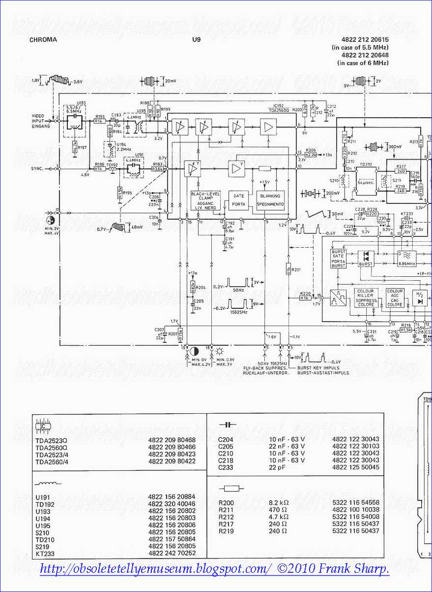


No comments:
Post a Comment
The most important thing to remember about the Comment Rules is this:
The determination of whether any comment is in compliance is at the sole discretion of this blog’s owner.
Comments on this blog may be blocked or deleted at any time.
Fair people are getting fair reply. Spam and useless crap and filthy comments / scrapers / observations goes all directly to My Private HELL without even appearing in public !!!
The fact that a comment is permitted in no way constitutes an endorsement of any view expressed, fact alleged, or link provided in that comment by the administrator of this site.
This means that there may be a delay between the submission and the eventual appearance of your comment.
Requiring blog comments to obey well-defined rules does not infringe on the free speech of commenters.
Resisting the tide of post-modernity may be difficult, but I will attempt it anyway.
Your choice.........Live or DIE.
That indeed is where your liberty lies.
Note: Only a member of this blog may post a comment.