


The AUTOVOX CHASSIS 130 was designed to be used with 30AX PHILIPS CRT TUBE AND PIL S4 VIDEOCOLOR FAMILY CRT TUBES.


All main functions of the chassis are modularized.
Was first and last chassis from AUTOVOX featuring the (Awesome) VIDEO IC MOTOROLA TDA3300
- SUPPLY + SYNCH S1018
- FRAME + E/W R1016
- VIDEO + CHROMA + RGB F.1017
- IF D0266
- TUNING CONTROL vst memotronic 32 SYNTH B.0779 b.0778
CIRCUITS DESCRIPTIONS:
AUTOVOX 32 TVC2271 CHASSIS 130 Television receiver with an automatic station finding arrangement:
MOTOROLA TUNING MEMORY / MEMOTRONIC SYSTEM TECHNOLOGY.In a radio or television receiver containing an automatic station finder with a digital counter, a clock
1. A receiver having automatic station finding capability, comprising:
means for tuning said receiver in response to an applied voltage;
a controllable pulse generator;
means for starting said pulse generator;
circulating counter means having parallel inputs and outputs, a stepping input and a set input, said stepping input connected to and responsive to pulses from said pulse generator for providing a variable digital output;
digital-to-analog converting means for converting the variable digital output from said counter means to a variable analog voltage, said voltage being applied to said tuning means, so that the receiver is tuned to a frequency corresponding to the analog voltage;
means for sensing a received signal and for providing a stop signal to the pulse generator in response thereto, whereby said generator stops providing pulses and the analog voltage remains constant keeping the receiver tuned to the received signal;
memory means having parallel inputs connected to the parallel outputs of said counter means and parallel outputs connected to the parallel inputs of said counter means;
means associated with said memory means for causing the memory means to store a particular digital output from said counter means; and
means associated with the set input of said counter means for selectively causing the digital signal at the counter input to be transferred to the counter output.
2. A receiver as described in claim 1, wherein the memory means comprises: two series connected parallel memories each having a transfer input, a first of said parallel memories having parallel inputs connected to the parallel outputs of the counter means and having the transfer input connected to the stop signal means, a second of said parallel memories having parallel outputs connected to the parallel inputs of the counter means and having the transfer input connected to the means for starting said pulse generator.
3. A receiver as described in claim 2, wherein each of said parallel memories comprises a plurality of semiconductor voltage flip-flops.
4. A receiver as described in claim 2, wherein the two series connected parallel memories are incorporated in an integrated circuit module with the counter means.
5. A receiver as described in claim 2, wherein the transfer input of the first parallel memory is also connected to the means associated with the set input of the counter means.
6. A receiver as described in claim 1, additionally comprising:
an additional memory means having parallel inputs and outputs;
means for connecting the inputs of said additional memory means to the counter means output and the outputs of said additional memory means to the counter inputs;
means for causing said additional memory means to store a digital output; and
means for transferring the stored digital output to the counter means input through the connecting means.
7. A receiver as described in claim 6, additionally comprising gate means disposed at the outputs of the memory means and the additional memory means for selectively connecting either the additional memory means or the memory means to the input of the counter.
8. A receiver as described in claim 6, wherein the additional memory means comprises a plurality of memories and the connecting means comprises a plurality of station switches corresponding in number to the number of additional memories.
9. A receiver as described in claim 1, wherein each memory means comprises a number of flip-flops corresponding to the number of digits to be stored.
Description:
The present invention relates to a radio or television receiver with an automatic station finding arrangement which contains a pulse generator, a circulating counter formed from semiconductor counting flip-flops and having parallel inputs, a digital-to-analog converter converting the count of the counter to a tuning voltage, and a start-stop circuit acting on the flow of counting pulses and controlled over a start and at least one stop line, and with a parallel memory connected between the parallel outputs and parallel inputs of the counter.
Such a radio receiver is known from, e.g., the journal "Funkschau 1971", pp. 535 to 538 and 587 to 589. With the aid of the free-running pulse generator, the up-counter, and the digital-to-analog converter, the automatic station finding arrangement generates a sawtoothlike tuning voltage for the varactors contained as frequency-setting tuning elements in the resonant circuits of the receiver's radio-frequency portion. If a transmitter is received which meets the receiving criteria set in the receiver, the pulse generator is stopped so that the tuning voltage now remains constant until the operator continues the automatic station finding operation by actuating a start switch.
It is frequently desirable to tune in once again the station at which the start switch for automatic station finding was actuated last - either for comparison or because of the more interesting program. To do this in the case of a receiver with provision for unidirectional automatic station search, the entire search range must be scanned once or several times by repeatedly actuating the start switch, depending on whether the desired station is detected immediately or not.
It is the object of the invention to provide measures for a receiver of the kind referred to by way of introduction which permit the transmitter received before the actuation of the start switch to be found again with a high degree of safety by simple manipulation.
The invention is characterized in that the parallel memory consists of two series-connected parallel memories having one transfer input each, that the transfer input of the (first) parallel memory, whose parallel inputs are connected to the parallel outputs of the counter, are connected directly or indirectly to the stop line, that the transfer input of the (second) parallel memory, whose parallel outputs are connected to the parallel inputs of the counter, is connected directly or indirectly
 to the start line, that the counter has a set input for through-connecting the parallel inputs of the counter to the flip-flops of the counter, and that a recall switch is connected to the set input of the counter.
Particularly advantageously, the memory locations of the two series-connected parallel memories are storage flip-flops using semiconductor technology. In that case it is possible to arrange the counter and the parallel memories on a common chip of an integrated-circuit module. Such a module has only two terminals more than a module formed by the counter only.
The measures characterized by the invention thus require, aside from an additional recall switch, no additional space and involve nearly no additional expense. To recall the station previously tuned in it is only necessary to depress a button, for example, whereby the receiver is safely tuned to the station's carrier wave even if at the instant of the depression the local received field strength is temporarily too low for sufficient reception.
The invention will now be described in more detail with reference to the accompanying drawing, showing, by way of example, two embodiments of the invention, and wherein:
FIG. 1 is a block diagram showing the radio- and intermediate-frequency portions of a receiver with an automatic station finding arrangement and a recall arrangement;
FIG. 2 shows diagrams a to g explaining the operation of the recall storage, and
FIG. 3 shows a receiver similar to the one of FIG. 1 in which the automatic station finding counter and the recall memories are arranged together on the chip of an integrated-circuit module.
The receivers shown in the block diagrams of FIGS. 1 and 3 have a radio-frequency-receiving section 1, an intermediate-frequency amplif ier 2, and a demodulator section 3, to whose output 4 are connected the arrangements processing the modulation frequency. The tunable resonant circuits of the radio-frequency section contain varactors as tuning elements. Connected to the radio-frequency section is an automatic station finding arrangement in which a digital-to-analog converter 5 generates from the count of a digital counter 7, which receives signals at a stepping input T and advances at the rate of a pulse generator 6, a nearly sawtooth-shaped tuning voltage for the varactors. With a sufficient received field strength at the antenna 8 of the receiver a signal is formed in the demodulator section 3 which signal can be used as stop signal 9 to change the state of a start-stop circuit 10 which may be a flip flop. In the "stop" state the start-stop circuit interrupts the pulse generation or the pulse flow in the pulse generator so that the receiver remains tuned to the station being received. By operating a start-button switch 11 a start signal 12 is generated in the receiver which signal places the start-stop circuit in the "automatic station finding" state and thus continues the automatic station finding operation until next station meeting the receiver's receiving requirements is received.
In the embodiment of FIG. 1, two series-connected parallel memories 15 and 16 are connected, respectively, over two groups of lines 13 and 14 consisting of n lines each, between the n outputs Q 11 to Q n1 and the parallel inputs A 11 to A n1 of the digital counter 7 containing n counting flip-flops. Each parallel memory contains n storage flip-flops and, besides the parallel bit inputs and outputs B and X, a transfer input S. If a transfer signal appears at the transfer input, the parallel memory records the bit word applied its parallel inputs B 1 to B n , which erases the previously entered bit word and now, in turn, appears at the memory outputs X 1 to X n .
The transfer input S of the parallel memory 15, whose parallel inputs are connected over the group of lines 13 to the outputs of the counter 7, is connected to the stop line 17, while the transfer input S of the parallel memory 16, whose parallel outputs are connected over the group of lines 14 to the parallel inputs of the counter 7, is connected to the start line 18.
 Connected to a set input P of the digital counters 7 is a switch 19 whose operation generates a set signal. The set signal sets the counter to a count which is equal to the bit word at the parallel inputs A 1 to A n of the counter. At the same time, the set signal acts over the line 20 and via an OR circuit provided for isolation on the transfer input S of the first parallel memory 15.
The diagrams a to g of FIG. 2 explain the operation of the automatic station finding arrangement in conjunction with the recall memories. In diagram a each of the blocks II, III, etc. represents the bit word for a count of the digital counter 7. The blocks in the diagrams b and c are the bit words which are stored in the parallel memories 15 and 16 and can be taken off the latter's parallel outputs, the blocks with equal Roman numerals (e.g. V) representing equal bit words. The diagram d shows the counting pulses 22 for the digital counter 7, the diagram e the stop pulses 9, the diagram f the start pulses 12, and the diagram g the set pulse 23 triggered by the recall switch 19.
The respective count from which the digital-to-analog converter 5 forms the tuning voltage for the varactors is applied simultaneously to the input of the digital-to-analog converter and, as a bit word (e.g. II, III, IV . . . , diagram a), to the input of the first parallel memory 15. At the occurence of a
stop signal 9 during the automatic station finding operation, the stop signal 9 acts as a transfer signal on the first parallel memory 15, and the count (e.g. V, diagram a) at which the stop pulse (e.g. 9a) was generated is entered into the first parallel memory 15 (V in diagram b). At the next start pulse 12a triggered via the start-button switch 11 the automatic station finding operation begins anew, starting from the instantaneous count (e.g. V, diagram a) of the counter. The start signal (12a in diagram f) acts as a transfer signal on the transfer input S of the second parallel memory 16, whereby the second parallel memory takes over the bit word (e.g. V) of the first. The next stop signal (e.g. 9b, diagram e) at a new count (e.g. VIII, diagram a) stops the automatic station search and enters the new count as a bit word (e.g. VIII, diagram b) into the first parallel memory 15.
If the operator operates the recall switch 19 so as to recall the setting to the previously received station, the set pulse 23 triggered by the recall switch sets the counter 7 to the count (e.g. V, diagram a) of the bit word (e.g. V, diagram c) stored in the second parallel memory 16, and the newly set count is entered into the first parallel memory 15 (e.g. V, diagram b). The next start signal (e.g. 12b, diagram f) initiates the automatic station finding operation as described.
In the embodiment of FIG. 3, the two series-connected parallel memories 15 and 16 are incorporated on the chip of an integrated-circuit module 25 which also comprises the circulating digital counter 7 and, for exam ple, the circuit 26 of a station memory device. The station memory device has the memory inputs D 1 to D n and the memory outputs Y 1 to Y n of its circuit 26 connected in parallel with the digital counter 7 in the same manner as the recall memory consisting of the two series-connected parallel memories 15 and 16. Therefore, gate circuits 27 and 28 are inserted between the parallel outputs of these memories and the parallel inputs A 1 to A n of the digital counter. The gate circuit 27 between the recall memory and the counter is opened by the set signal of the recall switch 19. The gate circuit 28 between the station memory and the counter is opened by the set signal of a switch 29 for calling the bit word of a station preselected by the station buttons 30. In front of the set input 8 of the digital counter the two set signals are separated from one another in an OR circuit 31.
In the embodiment of FIG. 3, the start-stop circuit 10 is designed in the manner of a flip-flop and can assume a "stop" state and an "automatic station finding" state. The transfer inputs S of the recall memory's parallel memories 15 and 16 are connected via the lines 32 and 33 to the outputs of the start-stop circuit. Since the signals at the outputs of the start-stop circuit are continuous signals, the lines 32 and 33 to the transfer inputs include pulse shapers 34 and 35, respectively.
In embodiments corresponding to FIG. 3 and having no station memory device, besides the circuit 26, the gate circuits 27 and 28 and the OR circuit 31 are omitted.
Such a radio receiver is known from, e.g., the journal "Funkschau 1971", pp. 535 to 538 and 587 to 589. With the aid of the free-running pulse generator, the up-counter, and the digital-to-analog converter, the automatic station finding arrangement generates a sawtoothlike tuning voltage for the varactors contained as frequency-setting tuning elements in the resonant circuits of the receiver's radio-frequency portion. If a transmitter is received which meets the receiving criteria set in the receiver, the pulse generator is stopped so that the tuning voltage now remains constant until the operator continues the automatic station finding operation by actuating a start switch.
It is frequently desirable to tune in once again the station at which the start switch for automatic station finding was actuated last - either for comparison or because of the more interesting program. To do this in the case of a receiver with provision for unidirectional automatic station search, the entire search range must be scanned once or several times by repeatedly actuating the start switch, depending on whether the desired station is detected immediately or not.
It is the object of the invention to provide measures for a receiver of the kind referred to by way of introduction which permit the transmitter received before the actuation of the start switch to be found again with a high degree of safety by simple manipulation.
The invention is characterized in that the parallel memory consists of two series-connected parallel memories having one transfer input each, that the transfer input of the (first) parallel memory, whose parallel inputs are connected to the parallel outputs of the counter, are connected directly or indirectly to the stop line, that the transfer input of the (second) parallel memory, whose parallel outputs are connected to the parallel inputs of the counter, is connected directly or indirectly
Particularly advantageously, the memory locations of the two series-connected parallel memories are storage flip-flops using semiconductor technology. In that case it is possible to arrange the counter and the parallel memories on a common chip of an integrated-circuit module. Such a module has only two terminals more than a module formed by the counter only.
The measures characterized by the invention thus require, aside from an additional recall switch, no additional space and involve nearly no additional expense. To recall the station previously tuned in it is only necessary to depress a button, for example, whereby the receiver is safely tuned to the station's carrier wave even if at the instant of the depression the local received field strength is temporarily too low for sufficient reception.
The invention will now be described in more detail with reference to the accompanying drawing, showing, by way of example, two embodiments of the invention, and wherein:
FIG. 1 is a block diagram showing the radio- and intermediate-frequency portions of a receiver with an automatic station finding arrangement and a recall arrangement;
FIG. 2 shows diagrams a to g explaining the operation of the recall storage, and
FIG. 3 shows a receiver similar to the one of FIG. 1 in which the automatic station finding counter and the recall memories are arranged together on the chip of an integrated-circuit module.
The receivers shown in the block diagrams of FIGS. 1 and 3 have a radio-frequency-receiving section 1, an intermediate-frequency amplif
 ier 2, and a demodulator section 3, to whose output 4 are connected the arrangements processing the modulation frequency. The tunable resonant circuits of the radio-frequency section contain varactors as tuning elements. Connected to the radio-frequency section is an automatic station finding arrangement in which a digital-to-analog converter 5 generates from the count of a digital counter 7, which receives signals at a stepping input T and advances at the rate of a pulse generator 6, a nearly sawtooth-shaped tuning voltage for the varactors. With a sufficient received field strength at the antenna 8 of the receiver a signal is formed in the demodulator section 3 which signal can be used as stop signal 9 to change the state of a start-stop circuit 10 which may be a flip flop. In the "stop" state the start-stop circuit interrupts the pulse generation or the pulse flow in the pulse generator so that the receiver remains tuned to the station being received. By operating a start-button switch 11 a start signal 12 is generated in the receiver which signal places the start-stop circuit in the "automatic station finding" state and thus continues the automatic station finding operation until next station meeting the receiver's receiving requirements is received.
In the embodiment of FIG. 1, two series-connected parallel memories 15 and 16 are connected, respectively, over two groups of lines 13 and 14 consisting of n lines each, between the n outputs Q 11 to Q n1 and the parallel inputs A 11 to A n1 of the digital counter 7 containing n counting flip-flops. Each parallel memory contains n storage flip-flops and, besides the parallel bit inputs and outputs B and X, a transfer input S. If a transfer signal appears at the transfer input, the parallel memory records the bit word applied its parallel inputs B 1 to B n , which erases the previously entered bit word and now, in turn, appears at the memory outputs X 1 to X n .
The transfer input S of the parallel memory 15, whose parallel inputs are connected over the group of lines 13 to the outputs of the counter 7, is connected to the stop line 17, while the transfer input S of the parallel memory 16, whose parallel outputs are connected over the group of lines 14 to the parallel inputs of the counter 7, is connected to the start line 18.
The diagrams a to g of FIG. 2 explain the operation of the automatic station finding arrangement in conjunction with the recall memories. In diagram a each of the blocks II, III, etc. represents the bit word for a count of the digital counter 7. The blocks in the diagrams b and c are the bit words which are stored in the parallel memories 15 and 16 and can be taken off the latter's parallel outputs, the blocks with equal Roman numerals (e.g. V) representing equal bit words. The diagram d shows the counting pulses 22 for the digital counter 7, the diagram e the stop pulses 9, the diagram f the start pulses 12, and the diagram g the set pulse 23 triggered by the recall switch 19.
The respective count from which the digital-to-analog converter 5 forms the tuning voltage for the varactors is applied simultaneously to the input of the digital-to-analog converter and, as a bit word (e.g. II, III, IV . . . , diagram a), to the input of the first parallel memory 15. At the occurence of a
If the operator operates the recall switch 19 so as to recall the setting to the previously received station, the set pulse 23 triggered by the recall switch sets the counter 7 to the count (e.g. V, diagram a) of the bit word (e.g. V, diagram c) stored in the second parallel memory 16, and the newly set count is entered into the first parallel memory 15 (e.g. V, diagram b). The next start signal (e.g. 12b, diagram f) initiates the automatic station finding operation as described.
In the embodiment of FIG. 3, the two series-connected parallel memories 15 and 16 are incorporated on the chip of an integrated-circuit module 25 which also comprises the circulating digital counter 7 and, for exam
 ple, the circuit 26 of a station memory device. The station memory device has the memory inputs D 1 to D n and the memory outputs Y 1 to Y n of its circuit 26 connected in parallel with the digital counter 7 in the same manner as the recall memory consisting of the two series-connected parallel memories 15 and 16. Therefore, gate circuits 27 and 28 are inserted between the parallel outputs of these memories and the parallel inputs A 1 to A n of the digital counter. The gate circuit 27 between the recall memory and the counter is opened by the set signal of the recall switch 19. The gate circuit 28 between the station memory and the counter is opened by the set signal of a switch 29 for calling the bit word of a station preselected by the station buttons 30. In front of the set input 8 of the digital counter the two set signals are separated from one another in an OR circuit 31.
In the embodiment of FIG. 3, the start-stop circuit 10 is designed in the manner of a flip-flop and can assume a "stop" state and an "automatic station finding" state. The transfer inputs S of the recall memory's parallel memories 15 and 16 are connected via the lines 32 and 33 to the outputs of the start-stop circuit. Since the signals at the outputs of the start-stop circuit are continuous signals, the lines 32 and 33 to the transfer inputs include pulse shapers 34 and 35, respectively.
In embodiments corresponding to FIG. 3 and having no station memory device, besides the circuit 26, the gate circuits 27 and 28 and the OR circuit 31 are omitted.
1. In an automatic fine tuning circuit including an integrated circuit chip having first and second contact areas for coupling to discrete circuit elements located external to said integrated circuit chip, apparatus comprising:
means located on said integrated circuit chip for supplying input signals having a frequency within a band including a predetermined reference frequency to said first and second contact areas;
a discriminator network, located external to said integrated circuit chip and coupled to said first and second contact areas, and responsive to said input signals for providing respective signals at said first and second contact areas which vary differentially in magnitude in response to the frequency deviation of said input signals from said reference frequency; and
first and second detector networks located on said integrated circuit chip and having respective input terminals direct current coupled to said first and second contact areas for detecting the magnitudes of said differentially varying signals.
2. In a television receiver, including a source of tuning voltage, and a tuner, including a reactive element responsive to said tuning voltage and an automatic frequency control signal, for producing a mixing signal to convert radio frequency television signals to intermediate frequency television signals within a band including a predetermined reference frequency, an automatic frequency control signal generator comprising:
first and second amplifiers, each having an input terminal for receiving a common intermediate frequency television signal having a frequency within a band including said predetermined reference frequency and an output terminal; said amplifiers supplying respective signal currents of like phase relationship to said output terminals in response to said common input signal;
a discriminator network coupled to said output terminals of said first and second amplifiers for causing respective signal voltages developed at said output terminals of said first and second amplifiers to vary differentially in magnitude in response to the frequency deviation of said intermediate frequency television signal from said reference frequency;
first and second detector networks respectively coupled to said output terminals of said first and second amplifiers for detecting the magnitudes of said differentially varying signal voltages;
a differential amplifier for developing output signals which vary differentially in sense and magnitude in response to the magnitudes of the signals detected by said first and second detector networks; and
means coupled to said differential amplifier for combining said output signals to develop an automatic frequency control signal which varies in sense and magnitude in response to the frequency deviation of said intermediate frequency signal from said predetermined reference frequency,
wherein said amplifiers, said detector networks, said differential amplifier, and said combining means and couplings therebetween are realized in integrated circuit form on a common monolithic integrated circuit chip, wherein each of said output terminals comprises an external connection terminal of said integrated circuit chip, wherein said discriminator network comprises components separate from said chip and coupled to said chip terminals, and wherein said automatic frequency control signal is coupled to said reactive element at a third chip terminal to control the frequency of said mixing signal.
3. The automatic frequency control signal generator of claim 2, further comprising:
a controllable current source having an input responsive to said tuning voltage and having an output coupled to said differential amplifier for varying the magnitude of the sum of said output signals for a given deviation of said intermediate frequency signals from said reference frequency, wherein said current source is located on said integrated circuit chip and said input is coupled to a fourth chip terminal to receive said tuning voltage.
4. In an automatic frequency control signal circuit including an integrated circuit chip having first, second and third contact areas for coupling to discrete circuit elements located external to said integrated circuit chip, apparatus comprising:
means located on said integrated circuit chip for supplying input signals having a frequency within a band including a predetermined reference frequency to said first and second contact areas;
a discriminator network, located external to said integrated circuit chip and coupled to said first and second contact areas, and responsive to said input signals for providing respective signals at said first and second contact areas which vary differentially in magnitude in response to the frequency deviation of said input signals from said reference frequency;
first and second detector networks located on said integrated circuit chip and having respective input terminals coupled to said first and second contact areas for detecting the magnitudes of said differentially varying signals;
a differential amplifier located on said integrated circuit chip and coupled to said detector networks for developing output signals which vary differentially in sense and magnitude in response to the detected magnitudes of said differentially varying signals; and
means located or said integrated circuit chip and coupled to said differential amplifier for combining said output signals to develop an automatic frequency control signal at said third contact area which varies in sense and magnitude in response to the frequency deviation of said input signals from said predetermined reference frequency.
5. The automatic frequency control signal circuit of claim 4, further comprising:
a controllable current source located on said integrated circuit chip and having an input coupled to a fourth contact area and an output coupled to said differential amplifier; and
means external to said integrated circuit chip and coupled to said fourth contact area for varying the magnitude of the sum of said output signals for a given deviation of said input signals from said predetermined reference frequency.
6. Frequency discriminating apparatus comprising:
means for supplying input signals having a frequency within a band including a predetermined reference frequency;
a discriminator network, coupled to said input signal means, which provides respective signals which vary differentially in magnitude in response to the frequency deviation of said input signals from said reference frequency;
means for detecting the respective magnitudes of said discriminator network signals;
an amplifier coupled to said detecting means for developing first and second output currents respectively representative of said respective signal magnitudes;
means for combining said first and second output currents to develop a difference current which is related in sense and magnitude to the frequency deviation of said input signals from said reference frequency; and
a controllable current source coupled to said amplifier for controlling the magnitude of the sum of said first and second output currents for a given frequency deviation of said input signals from said reference frequency.
7. Frequency discriminating apparatus comprising:
means for supplying input signals having a frequency within a band including a predetermined reference frequency;
a discriminator network, coupled to said input signal means, which provides respective signals which vary differentially in magnitude in response to the frequency deviation of said input signals from said reference frequency;
means for detecting the respective magnitudes of said discriminator network signals;
an amplifier coupled to said detecting means for developing first and second output currents respectively representative of said respective signal magnitudes;
means for combining said first and second output currents to develop a difference current which is related in sense and magnitude to the frequency deviation of said input signals from said reference frequency; and
first and second transistors each disposed in a common base amplifier configuration to receive one of said respective output currents from said amplifier and having respective output electrodes coupled to said current combining means.
8. Frequency discriminating apparatus comprising:
means for supplying input signals having a frequency within a band including a predetermined reference frequency;
first and second terminals;
first and second transistors each having an input electrode coupled to said input signal supplying means and respective output electrodes coupled to said first and second terminals for supplying signals of like phase relationship at said terminals;
a discriminator network coupled to said first and second terminals for causing the signals developed at said first and second terminals to vary differentially in magnitude in response to the frequency deviation of said input signals from said reference frequency;
means for detecting the magnitudes of said differentially varying signals; and
a differential amplifier responsive to the detected magnitudes of said differentially varying signals for developing an output signal which varies in sense and magnitude in response to the frequency deviation of said input signals from said reference frequency,
wherein said discriminator network is tuned to said reference frequency and comprises:
a first parallel combination of a capacitor and an intermediate tapped inductor, coupled between said first and second terminals; and
a second parallel combination of a capacitor and an inductor, coupled between said intermediate tap of said inductor of said first parallel combination, and a source of supply voltage.
9. In a television receiver, automatic frequency control apparatus for providing an automatic frequency control signal which varies in response to the frequency deviation of an intermediate frequency signal from a predetermined reference frequency, comprising:
means responsive to said intermediate frequency signal for providing first and second input signals of like phase relationship;
a discriminator network, coupled to said input signal means, and responsive to said first and second input signals, for causing said input signals to vary differentially in magnitude in response to the frequency deviation of said input signals from said reference frequency;
means coupled to the junction of said input signal means and said discriminator network for detecting the magnitudes of said differentially varying signals;
a differential amplifier coupled to said detecting means for developing output signals which vary in sense and magnitude in response to the detected magnitudes of said differentially varying signals; and
a current mirror circuit coupled to said differential amplifier for combining said output signals to develop an automatic frequency control signal which varies in sense and magnitude in response to the frequency deviation of said intermediate frequency signal from said predetermined reference frequency, wherein said automatic frequency control signal may be used to control the frequency of said intermediate frequency signal.
a controllable current source coupled to said differential amplifier and having an input for controlling the magnitude of the sum of the output signals developed by said differential amplifier for a given deviation of said intermediate frequency signal from said reference frequency.
11. In a television receiver, including a source of tuning voltage, and a tuner, including a reactive element responsive to said tuning voltage and an automatic frequency control signal, for producing a mixing signal to convert radio frequency television signals to intermediate frequency television signals within a band including a predetermined reference frequency, an automatic frequency control signal generator comprising:
means responsive to said intermediate frequency signals for developing signals which vary differentially in magnitude in response to the frequency deviation of said intermediate frequency signals from said reference frequency;
a differential amplifier for developing output signals which vary differentially in sense and magnitude in response to the magnitudes of the signals developed by said differential signal means; and
means coupled to said differential amplifier for combining said output signals to develop an automatic frequency control signal which varies in sense and magnitude in response to the frequency deviation of said intermediate frequency signal from said predetermined reference frequency, wherein said automatic frequency control signal is coupled to said reactive element to control the frequency of said mixing signal.
12. The automatic frequency control signal generator of claim 11, further comprising:
a controllable current source responsive to said tuning voltage and having an output coupled to said differential amplifier for varying the magnitude of the sum of said output signals for a given deviation of said intermediate frequency signals from said reference frequency.
Description:
This invention relates to automatic frequency control apparatus in general, and, in particular, to such apparatus for deriving a frequency dependent error-correction signal to control the tuning of a local oscillator in a superheterodyne receiver.
It is the function of a television tuner to select a narrow range of frequencies from among the many broadcast frequencies in the radio frequency band. A conventional television tuner performs this function through the use of a radio frequency amplifier, a mixer, and a local heterodyne oscillator. The output of this oscillator is compared to, or beat with, the radio frequency television signal received from the receiver antenna by the mixer. This beating action creates both the sum and difference frequencies of the original radio frequency and local oscillator frequencies. All but the difference frequencies, called intermediate frequencies (I.F.), are filtered out. These I.F. frequencies are amplified and detected by the television receiver to recreate the desired sound and picture information.
In order to provide the optimum image on the television screen, together with accurate sound reproduction, it is necessary that the receiver local oscillator be adjusted so that the picture and sound carriers are located at the correct points in the I.F. passband of the television receiver. This is especially true in the tuning of color television receivers. Not only must the picture and sound carriers be situated at their proper positions in the I.F. passband but the color subcarrier must also be properly positioned in order that the colors will be reproduced by the kinescope with proper hue and saturation characteristics. If the local oscillator is for any reason not set at the proper frequency, the intermediate frequencies will be incorrect, and may deleteriously affect the reproduced sound and picture. As is well known, this mistuning may be due to improper fine tuning by the television viewer, local oscillator drift, or inaccurate resetability of the detenting action of a mechanical tuner. In order to overcome these problems, conventional receivers are provided with means for compensating for variations in the intermediate frequencies.
This compensation is normally accomplished by deriving an automatic fine tuning (AFT) voltage from the output of the I.F. amplifying stage of the receiver. The AFT voltage is representative of the sense and degree that the I.F. signal departs from the desired I.F. signal. The AFT voltage is applied to a voltage responsive reactance device in the local oscillator to correct the mistuning of the oscillator and thereby optimize the sound and picture reproduction.
There are presently two types of AFT circuits in general use: the quadrature detector type and the differential envelope detector type. The quadrature detector type AFT circuit converts frequency shifts of a frequency modulated signal to differentially phase-shifted signals by applying the frequency modulated signal to a filter network, which develops two differentially phase-shifted, or delayed, signals at its output ports. The differentially phase-shifted signals are coupled to a quadrature, or phase, detector, which converts the relative phase difference between the signals at the filter output ports to an amplitude-varying AFT control signal. The differential envelope detector type AFT circuit, such as that described in the present application, utilizes a linear filter network to convert frequency shifts of a frequency modulated signal to differentially related, amplitude varying signals. These signals are coupled to envelope detectors, which convert the amplitude varying signals to AFT control signals. The differential envelope detector AFT circuit generally requires fewer components than the quadrature detector type, and is preferred in many applications because of its ability to produce a narrower, more precisely controlled AFT bandwidth. The narrower bandwidth reduces the effect of I.F. noise on the AFT control system and produces sharper AFT response in the vicinity of the I.F. picture carrier being controlled by the system.
In order to minimize the size and number of components required to construct an AFT circuit, it is desirable to fabricate the circuit in integrated circuit form on a single monolithic integrated circuit chip. However, certain AFT circuit elements, specifically, the reactive components used to construct the discriminator network necessary to convert frequency shifts of the I.F. signal to amplitude modulated signals, do not readily lend themselves to integrated circuit fabrication and must be located external to the I.C. chip. The I.C. chip has only a limited number of external connection points, or terminals, for connection to external components. Hence, it is desirable to construct the AFT circuit in a manner which reduces the number of required connections to external components.
In accordance with the principles of the present invention, an AFT circuit is provided which generates AFT control signals in response to a video I.F. signal. The I.F. signal is supplied to the inputs of two buffer amplifiers, which couple parallel signals of like phase relationship to two inputs of a discriminator network. The discriminator network is tuned to the desired I.F. frequency, and is responsive to the buffered I.F. signals for providing respective signals at its inputs which vary differentially in sense and degree with the frequency deviation of the buffered I.F. signals from the desired I.F. frequency. The differentially related signals are detected by two peak detector networks for use as AFT control signals. The buffer amplifiers and peak detector networks may be conveniently fabricated on a single I.C. chip. The discriminator network is coupled to the buffer amplifiers and peak detectors through two external I.C. terminals.
The peak detected signals may be combined and amplified to produce an AFT signal for application to the local oscillator. However, a circuit with an AFT signal which varies over a fixed voltage range is restricted to operation with local oscillators which respond to the specific voltage range of that circuit. Such an AFT circuit can be used with a wide variety of local oscillators of differing characteristics only if additional interfacing circuitry is interposed between the AFT circuit and the local oscillator. Such interfacing circuitry can add undesirable delays and complexity to the AFT system.
In accordance with a further aspect of the present invention, the detected, differentially related signals are combined by a differential amplifier and coupled to a current mirror circuit to provide an AFT current signal. The current mirror circuit is contained on the same I.C. chip as the buffer amplifiers and detector networks. Through the use of a suitable external load resistor, the AFT current signal may be used to produce a wide variety of AFT voltage ranges. In addition, means are provided for varying the magnitude of the AFT current signal to permit accurate matching of the AFT circuit to the signal requirements of the local oscillator. The magnitude of the AFT current signal may be modified during operation of the television receiver, for example, to provide continuously variable AFT current signal ranges over the full range of television channels.
Tuning Search + Drive
Employs the Motorola Tuning Memory System.
a complex circuitry with mixed signals technology.
- UAA1008 (Tuning Drive + AFC)
-MC14426 (Memory Control)
TDA2581 CONTROL CIRCUIT FOR SMPS (PHILIPS):
The TDA2581 is a monolithic integrated circuit
for controlling switched-mode power supplies (SMPS) which are provided with the drive for the horizontal deflection stage.The circuit features the following:
— Voltage controlled horizontal oscillator.
— Phase detector.
— Duty factor control for the positive-going transient of the output signal.
— Duty factor increases from zero to its normal operation value.
— Adjustable maximum duty factor.
- Over-voltage and over-current protection with automatic re-start after switch-off.
— Counting circuit for permanent switch-off when n~times over~current or over-voltage is sensed
-Protection for open-refere
 nce voltage.
- Protection for too low supply voltage.
Protection against loop faults.
Positive tracking of duty factor and feedback voltage when the feedback voltage is smaller than the
reference voltage minus 1,5 V.
THIS IC WAS USED IN PHILIPS CHASSIS K12 AND PHILIPS K30 AND PHILIPS K35 AND PHILIPS KT2 AND PHILIPS KT3 AND SOME K40 !
TDA2541 IF AMPLIFIER WITH DEMODULATOR AND AFC

DESCRIPTION
The TDA2540 an
d 2541 are IF amplifier and A.M.demodulator circuits for colour and black and white
televisionreceiversusingPNPorNPNtuners. They
are intended for reception of negative or positive
modulation CCIR standard.
They incorporate the following functions :
.Gain controlled amplifier .Synchronous demodulator
.White spot inverter .Video preamplifier with noise protection
.Switchable AFC .AGC with noise gating
.Tuner AGC output (NPN tuner for 2540)-(PNP
tuner for 2541)
.VCR switch for video output inhibition (VCR play back)
- VIDEO CHROMA PROCESSING WITH TDA3300 (MOTOROLA)

TDA3300 3301 TV COLOR PROCESSOR
The Decoder IC The centre -piece of the decoder is the Motorola TDA3300B i.c. which carries out all the luminance and U V Inputs from PAL delay line 9V Frequency nlyv Z 2RV2 100k chroma signal processing required. Features of this 40 -pin chip include: (1) Automatic black -current control via feedback from the RGB output circuits. (2) Peak beam current limiting to prevent blooming on highlights - in addition to the normal beam current limit- ing action. (3) Separate R, G and B input pins for the injection of teletext/data signals (or on -screen display of the channel number with frequency synthesis tuning). These signals can be varied by means of the user brightness and con- trast controls. (4) Low dissipation - about 600mW. (5) By adding a small adaptor panel with a TDA3030A SECAM-to-PAL converter i.c. during production the receiver is given multistandard (PAL, SECAM and NTSC-4.43) capability.

 A
block diagram of the TDA3300B i.c. is shown in Fig. 3. As with the
better known TDA3560 single -chip decoder, both the chroma and the burst
pass through the chroma delay line. The U output from this enters the
TDA3300B at pin 8, passing to the U detector and to the burst detector.
The latter is part of a phase -locked loop, the detector's output being
applied via an H/2 (half-line frequency) switch to the 4.43MHz voltage
-controlled crystal oscillator. The 4.43MHz reference oscillator's
output is applied for PAL switching, and to the U detector via a voltage
-controlled 90° phase shifter. This shifter is under the control of the
90° detec- tor which compares its output with the oscillator's output
coming via the PAL switch: when the phase shift is cor- rect, the output
from the 90° phase detector is zero. The combined effect of the two H/2
switches in the reference oscillator control loop - the two shown on
the right-hand side - cancels phase detector offsets. The outputs from
the U and V detectors include burst "flag" pulses which are used for
a.c.c., ident and colour -killing - there are two colour -killing
actions. RGB Output Stages The RGB output stages are of the class AB
type and incorporate extra circuitry for c.r.t. black -current sampl-
ing and beam limiting. Fig. 4 shows the red output stage. Under most
conditions transistor 2TR1 acts as a class A amplifier, driving the
tube's cathode via 2D5 and 2TR7. A high -value collector load resistor
(2R33) is used to reduce the dissipation in 2TR1. The stage gain is set
by the ratio of 2R40 and 2R36 to 2R25 and 2RV3, the latter setting the
drive level. For good transient response it's necessary for the
tube/base capacitance to be rapidly charged/discharged in accordance
with the signal swings. There is no problem when 2TR1 is being driven
from off to on, since the capacitance is discharged rapidly via 2D5 and
2TR1. When 2TR1 is driven from on to off however 2D5 will become reverse
biased. Under these conditions 2TR4 acts as an emitter -follower so
that the capacitance charges rapidly. Black -level stability is critical
for good results. As we've 2R46 5k6 2R51 120k 2TR7 BF493S 2C43l
Sampling circuit L -J 1k5 Field blanking J Red cathode _Tube input T"and
base 810capacitance nlrr Reference Line pedestal blanking Sample -and -
hold amplifier-ws switched on rt- Video Urn seen, the TDA3300B chip
incorporates circuitry for automatic black -current correction. Making
use of this reduces service calls and ensures constant performance
despite tube ageing or circuit misadjustment. Feedback is required, and
this is provided by the sampling circuit shown in the box with the
broken outline. Transistor 2TR7 acts as an emitter -follower between the
video output stage and the c.r.t.'s cathode. It's a low leakage type,
the components 2C40, 2D10 and 2C43 ensuring that the circuit has
negligible effect on the video signal. Since the beam current flows via
2R51, a voltage proportional to the beam current is produced across this
resistor. It's fed into the TDA3300B at pin 22. Black -current Control
For automatic black -current control the important thing is the small
beam current that flows when the tube is biased just above cut off. To
enable this current to be sampled, the TDA3300B replaces the video
signal with a fixed reference pedestal voltage for a couple of lines at
the end of each field blanking period (this pedestal can be seen as a
grey line at the top of the picture if the height control's setting is
reduced). The sample voltage at pin 22 of the i.c. is fed to one input
of a sample -and -hold amp- lifier which is switched on to sample the
input for one line only of the reference pedestal period. 2C33 acts as
the black -current control reservoir capacitor, holding the charge
acquired during the sampling time for the whole field period. This
charge is added to the video signal within the i.c., thus maintaining
the correct red gun black current. It's interesting to notice that when a
set is switched on from cold there's a momentary screen bright -up with
flyback lines as the beam current begins to flow. This is because it
takes several fields for 2C33 (and the corre- sponding capacitors in the
green and blue channels) to charge fully. Since the voltage
continuously available across 2R51 is proportional to beam current, it's
used within the i.c. for peak beam current limiting during the active
line periods. This is in addition to beam current limiting via the con-
trast control - and a crowbar trip that operates should the beam current
exceed 3mA.
A
block diagram of the TDA3300B i.c. is shown in Fig. 3. As with the
better known TDA3560 single -chip decoder, both the chroma and the burst
pass through the chroma delay line. The U output from this enters the
TDA3300B at pin 8, passing to the U detector and to the burst detector.
The latter is part of a phase -locked loop, the detector's output being
applied via an H/2 (half-line frequency) switch to the 4.43MHz voltage
-controlled crystal oscillator. The 4.43MHz reference oscillator's
output is applied for PAL switching, and to the U detector via a voltage
-controlled 90° phase shifter. This shifter is under the control of the
90° detec- tor which compares its output with the oscillator's output
coming via the PAL switch: when the phase shift is cor- rect, the output
from the 90° phase detector is zero. The combined effect of the two H/2
switches in the reference oscillator control loop - the two shown on
the right-hand side - cancels phase detector offsets. The outputs from
the U and V detectors include burst "flag" pulses which are used for
a.c.c., ident and colour -killing - there are two colour -killing
actions. RGB Output Stages The RGB output stages are of the class AB
type and incorporate extra circuitry for c.r.t. black -current sampl-
ing and beam limiting. Fig. 4 shows the red output stage. Under most
conditions transistor 2TR1 acts as a class A amplifier, driving the
tube's cathode via 2D5 and 2TR7. A high -value collector load resistor
(2R33) is used to reduce the dissipation in 2TR1. The stage gain is set
by the ratio of 2R40 and 2R36 to 2R25 and 2RV3, the latter setting the
drive level. For good transient response it's necessary for the
tube/base capacitance to be rapidly charged/discharged in accordance
with the signal swings. There is no problem when 2TR1 is being driven
from off to on, since the capacitance is discharged rapidly via 2D5 and
2TR1. When 2TR1 is driven from on to off however 2D5 will become reverse
biased. Under these conditions 2TR4 acts as an emitter -follower so
that the capacitance charges rapidly. Black -level stability is critical
for good results. As we've 2R46 5k6 2R51 120k 2TR7 BF493S 2C43l
Sampling circuit L -J 1k5 Field blanking J Red cathode _Tube input T"and
base 810capacitance nlrr Reference Line pedestal blanking Sample -and -
hold amplifier-ws switched on rt- Video Urn seen, the TDA3300B chip
incorporates circuitry for automatic black -current correction. Making
use of this reduces service calls and ensures constant performance
despite tube ageing or circuit misadjustment. Feedback is required, and
this is provided by the sampling circuit shown in the box with the
broken outline. Transistor 2TR7 acts as an emitter -follower between the
video output stage and the c.r.t.'s cathode. It's a low leakage type,
the components 2C40, 2D10 and 2C43 ensuring that the circuit has
negligible effect on the video signal. Since the beam current flows via
2R51, a voltage proportional to the beam current is produced across this
resistor. It's fed into the TDA3300B at pin 22. Black -current Control
For automatic black -current control the important thing is the small
beam current that flows when the tube is biased just above cut off. To
enable this current to be sampled, the TDA3300B replaces the video
signal with a fixed reference pedestal voltage for a couple of lines at
the end of each field blanking period (this pedestal can be seen as a
grey line at the top of the picture if the height control's setting is
reduced). The sample voltage at pin 22 of the i.c. is fed to one input
of a sample -and -hold amp- lifier which is switched on to sample the
input for one line only of the reference pedestal period. 2C33 acts as
the black -current control reservoir capacitor, holding the charge
acquired during the sampling time for the whole field period. This
charge is added to the video signal within the i.c., thus maintaining
the correct red gun black current. It's interesting to notice that when a
set is switched on from cold there's a momentary screen bright -up with
flyback lines as the beam current begins to flow. This is because it
takes several fields for 2C33 (and the corre- sponding capacitors in the
green and blue channels) to charge fully. Since the voltage
continuously available across 2R51 is proportional to beam current, it's
used within the i.c. for peak beam current limiting during the active
line periods. This is in addition to beam current limiting via the con-
trast control - and a crowbar trip that operates should the beam current
exceed 3mA.This device will accept a PAL or NTSC composite video signal and output the
three color signals, needing only a simple driver amplifier to interface to the pic-
ture tube. The provision of high bandwidth on-screen display inputs makes it
suitable for text display, TV games, cameras, etc. The TDA3301 B has user con»
trol laws, and also a phase shift control which operates in PAL, as well as NTSC.
0 Automatic Black Level Setup
0 Beam Current Limiting
0 Uses Inexpensive 4.43 MHZ to 3.58 MHz Crystal
0 No Oscillator Adjustment Required
0 Three OSD Inputs Plus Fast Blanking Input
0 Four DC, High Impedance User Controls
0 lnterlaces with TDA33030B SECAM Adaptor
0 Single 12 V Supply
0 Low Dissipation, Typically 600 mW
The brilliance control operates by adding a pedestal to the output
signals. The amplitude of the pedestal is controlled by Pin 30.
During CRT beam current sampling a standard pedestal is
substituted, its value being equivalent tothe value given by V30 Nom
Brightness at black level with V30 Nom is given by the sum of three gun
currents at the sampling level, i.e. 3x20 |.1A with 100 k reference
resistors on Pins 16, 19, and 22.
During picture blanking t
he brilliance pedestal is zero; therefore, theoutput voltage during blanking is always the minimum brilliance black
level (Note: Signal channels are also gain blanked).
Chrominance Decoder
The chrominance decoder section of the TDA3301 B
consists of the following blocks:
Phase-locked reference oscillator;
Phase-locked 90 degree servo loop;
U and V axis decoders
ACC detector and identification detector; .
Identification circuits and PAL bistable; .
Color difference filters and matrixes with fast blanking
Circuits.
The major design considerations apart from optimum
performance were:
o A minimum number of factory adjustments,
o A minimum number of external components,
0 Compatibility with SECAM adapter TDA3030B,
0 Low dissipation,
0 Use of a standard 4.433618 Mhz crystal rather
than a 2.0 fc crystal with a divider.
The crystal VCO is of the phase shift variety in which the
frequency is controlled by varying the phase of the feedback.
A great deal of care was taken to ensure that the oscillator loop
gain and the crystal loading impedance were held constant in
order to ensure that the circuit functions well with low grade
crystal (crystals having high magnitude spurious responses
can cause bad phase jitter). lt is also necessary to ensure that
the gain at third harmonic is low enough to ensure absence of
oscillation at this frequency.
It can be seen that the
necessary 1 45°C phase shift is obtained by variable addition
ol two currents I1 and I2 which are then fed into the load
resistance of the crystal tuned circuit R1. Feedback is taken
from the crystal load capacitance which gives a voltage of VF
lagging the crystal current by 90°.
The RC network in the T1 collector causes I1 to lag the
collector current of T1 by 45°.
For SECAM operation, the currents I1 and I2 are added
together in a fixed ratio giving a frequency close to nominal.
When decoding PAL there are two departures from normal
chroma reference regeneration practice:
a) The loop is locked to the burst entering from the PAL
delay line matrix U channel and hence there is no
alternating component. A small improvement in signal
noise ratio is gained but more important is that the loop
filter is not compromised by the 7.8 kHz component
normally required at this point for PAL identification
b) The H/2 switching of the oscillator phase is carried out
before the phase detector. This implies any error signal
from the phase detector is a signal at 7.8 kHz and not dc.
A commutator at the phase detector output also driven
from the PAL bistable coverts this ac signal to a dc prior
to the loop filter. The purpose ot this is that constant
offsets in the phase detector are converted by the
commutator to a signal at 7.8 kHz which is integrated to
zero and does not give a phase error.
When used for decoding NTSC the bistable is inhibited, and
slightly less accurate phasing is achieved; however, as a hue
control is used on NTSC this cannot be considered to be a
serious disadvantage.
90° Reference Generation
To generate the U axis reference a variable all-pass network
is utilized in a servo loop. The output of the all-pass network
is compared with the oscillator output with a phase detector of
which the output is filtered and corrects the operating point of
the variable all»pass network .
As with the reference loop the oscillator signal is taken after
the H/2 phase switch and a commutator inserted before the
filter so that constant phase detector errors are cancelled.
For SECAM operation the loop filter is grounded causing
near zero phase shift so that the two synchronous detectors
work in phase and not in quadralure.
The use of a 4.4 MHz oscillator and a servo loop to generate
the required 90° reference signal allows the use of a standard,
high volume, low cost crystal and gives an extremely accurate
90° which may be easily switched to 0° for decoding AM
SECAM generated by the TDA3030B adapter.
ACC and Identification Detectors
During burst gate time the output components of the U and
also the V demodulators are steered into PNP emitters. One
collector current of each PNP pair is mirrored and balanced
against its twin giving push-pull current sources for driving the
ACC and the identification filter capacitors.
The identification detector is given an internal offset by
making the NPN current mirror emitter resistors unequal. The
resistors are offset by 5% such that the identification detector
pulls up on its filter capacitor with zero signal.
Identification
See Figure 11 for definitions.
Monochrome I1 > I2
PAL ldent. OK I1 < lg
PAL ldent_ X l1 > I2
NTSC I3 > I2
Only for correctly identified PAL signal is the capacitor
voltage held low since I2 is then greater than I1.
For monochrome and incorrectly identified PAL signals l1>l2
hence voltage VC rises with each burst gate pulse.
When V,ef1 is exceeded by 0.7 V Latch 1 is made to conduct
which increases the rate of voltage rise on C. Maximum
current is limited by R1.
When Vref2
is exceeded by 0.7 V then Latch 2 is made toconduct until C is completely discharged and the current drops
to a value insufficient to hold on Latch 2.
As Latch 2 turns on Latch 1 must turn off.
Latch 2 turning on gives extra trigger pulse to bistable to
correct identification.
The inhibit line on Latch 2 restricts its conduction to alternate
lines as controlled by the bistable. This function allows the
SECAM switching line to inhibit the bistable operation by firing
Latch 2 in the correct phase for SECAM. For NTSC, Latch 2
is fired by a current injected on Pin 6.
lf the voltage on C is greater than 1.4 V, then the saturation
is held down. Only for SECAM/NTSC with Latch 2 on, or
correctly identified PAL, can the saturation control be
anywhere but minimum.
NTSC Switch
NTSC operation is selected when current (I3) is injected into
Pin 6. On the TDA33O1 B this current must be derived
externally by connecting Pin 6 to +12 V via a 27 k resistor (as
on TDA33OOB). For normal PAL operation Pin 40 should be
connected to +12 V and Pin 6 to the filter capacitor.
4 Color Difference Matrixing, Color Killing,
and Chroma Blanking
During picture time the two demodulators feed simple RC
filters with emitter follower outputs. Color killing and blanking
is performed by lifting these outputs to a voltage above the
maximum value that the color difference signal could supply.
The color difference matrixing is performed by two
differential amplifiers, each with one side split to give the
correct values of the -(B-Y) and -(Ft-Y) signals. These are
added to give the (G-Y) signal.
The three color difference signals are then taken to the
virtual grounds of the video output stages together with
luminance signal.
Sandcastle Selection
The TDA3301B may be used with a two level sandcastle
and a separate frame pulse to Pin 28, or with only a three level
(super) sandcastle. In the latter case, a resistor of 1.0 MQ is
necessary from + 12 V to Pin 28 and a 70 pF capacitor from
Pin 28 to ground.
Timing Counter for Sample Control
In order to control beam current sampling at the beginning
of each frame scan, two edge triggered flip-flops are used.
The output K ofthe first flip-flop A is used to clock the second
tlip-flop B. Clocking of A by the burst gate is inhibited by a count
of A.B.
The count sequence can only be initiated by the trailing
edge of the frame pulse. ln order to provide control signals for:
Luma/Chroma blanking
Beam current sampling
On-screen display blanking
Brilliance control
The appropriate flip-flop outputs ar matrixed with sandcastle
and frame signals by an emitter-follower matrix.
Video Output Sections
Each video output stage consists of a feedback amplifier in A further drive current is used to control the DC operating
which the input signal is a current drive to the virtual earth from point; this is derived from the sample and hold stage which
the luminance, color difference and on-screen display stages. samples the beam current after frame flyback.
AUTOVOX TVC2271 CHASSIS 130 CIRCUIT ARRANGEMENT IN A PICTURE DISPLAY DEVICE UTILIZING A STABILIZED SUPPLY VOLTAGE CIRCUIT:
A stabilized supply voltage circuit for a picture display device comprising a chopper wherein the switching signal has the line frequency and is duration-modulated. The coil of the chopper constitutes the primary winding of a transformer a secondary winding of which drives the line output transistor so that the switching transistor of the chopper also functions as a driver for the line output stage. The oscillator generating the switching signal may be the line oscillator. In a special embodiment the driver and line output transistor conduct simultaneously and in order to limit the base current of the line output transistor a coil shunted by a diode is incorporated in the drive line of the line output transistor. Other secondary windings of the transformer drive diodes which conduct simultaneously with the efficiency diode of the chopper so as to generate further stabilized supply voltages.
Description:
The invention relates to a circuit arrangement in a picture display device wherein the input direct voltage between two input terminals, which is obtained be rectifying the mains alternating voltage, is converted into a stabilized output direct voltage by means of a switching transistor and a coil and wherein the transistor is connected to a first input terminal and an efficiency diode is connected to the junction of the transistor and the coil. The switching transistor is driven by a pulsatory voltage of line frequency which pulses are duration-modulated in order to saturate the switching transistor during part of the period dependent on the direct voltage to be stabilized and to cut off this transistor during the remaining part of the period. The pulse duration modulation is effected by means of a comparison circuit which compares the direct voltage to be stabilized with a substantially constant voltage, the coil constituting the primary winding of a transformer. Such a circuit arrangement is known from German "Auslegeschrift" 1.293.304. wherein a circuit arrangement is described which has for its object to convert an input direct voltage which is generated between two terminals into a different direct voltage. The circuit employs a switch connected to the first terminal of the input voltage and periodically opens and closes so that the input voltage is converted into a pulsatory voltage. This pulsatory voltage is then applied to a coil. A diode is arranged between the junction of the switch and the coil and the second terminal of the input voltage whilst a load and a charge capacitor in parallel thereto are arranged between the other end of the coil and the second terminal of the input voltage. The assembly operates in accordance with the known efficiency principle i.e., the current supplied to the load flows alternately through the switch and through the diode. The function of the switch is performed by a switching transistor which is driven by a periodical pulsatory voltage which saturates this transistor for a given part of the period. Such a configuration is known under different names in the literature; it will be referred to herein as a "chopper." A known advantage thereof, is that the switching transistor must be able to stand a high voltage or provide a great current but it need not dissipate a great power. The output voltage of the chopper is compared with a constant reference voltage. If the output voltage attempts to vary because the input voltage and/or the load varies, a voltage causing a duration modulation of the pulses is produced at the output of the comparison arrangement. As a result the quantity of the energy stored in the coil varies and the output voltage is maintained constant. In the German "Auslegeschrift" referred to it is therefore an object to provide a stabilized supply voltage device.
In the circuit arrangement according to the mentioned German "Auslegeschrift" the frequency of the load variations or a harmonic thereof is chosen as the frequency for the switching voltage. Particularly when the load fed by the chopper is the line deflection circuit of a picture display device, wherein thus the impedance of the load varies in the rhythm of the line frequency, the frequency of the switching voltage is equal to or is a multiple of the line frequency.
It is to be noted that the chopper need not necessarily be formed as that in the mentioned German "Auslegeschrift." In fact, it is known from literature that the efficiency diode and the coil may be exchanged. It is alternatively possible for the coil to be provided at the first terminal of the input voltage whilst the switching transistor is arranged between the other end and the second terminal of the input voltage. The efficiency diode is then provided between the junction of said end and the switching transistor and the load. It may be recognized that for all these modifications a voltage is present across the connections of the coil which voltage has the same frequency and the same shape as the pulsatory switching voltage. The control voltage of a line deflection circuit is a pulsatory voltage which causes the line output transistor to be saturates and cut off alternately. The invention is based on the recognition that the voltage present across the connections of the coil is suitable to function as such a control voltage and that the coil constitutes the primary of a transformer. To this end the circuit arrangement according to the invention is characterized in that a secondary winding of the transformer drives the switching element which applies a line deflection current to line deflection coils and by which the voltage for the final anode of a picture display tube which forms part of the picture display device is generated, and that the ratio between the period during which the switching transistor is saturated and the entire period, i.e., the switching transistor duty cycle is between 0.3 and 0.7 during normal operation.The invention is also based on the recognition that the duration modulation which is necessary to stabilize the supply voltage with the switching transistor does not exert influence on the driving of the line output transistor. This resides in the fact that in case of a longer or shorter cut-off period of the line output transistor the current flowing through the line deflection coils thereof is not influenced because of the efficiency diode current and transistor current are taken over or, in case of a special kind of transistor, the collector-emitter current is taken over by the base collector current and conversely. However, in that case the above-mentioned ratios of 0.3 : 0.7 should be taken into account since otherwise this take-over principle is jeopardized.As will be further explained the use of the switching transistor as a driver for the line output transistor in an embodiment to be especially described hereinafter has the further advantage that the line output transistor automatically becomes non-conductive when this switching transistor is short circuited so that the deflection and the EHT for the display tube drop out and thus avoid damage thereof.Due to the step according to the invention the switching transistor in the stabilized supply functions as a driver for the line deflection circuit. The circuit arrangement according to the invention may in addition be equipped with a very efficient safety circuit so that the reliability is considerably enhanced, which is described in the U.S. Pat. No. 3,629,686. The invention is furthermore based on the recognition of the fact that the pulsatory voltage present across the connections of the coil is furthermore used and to this end the circuit arrangement according to the invention is characterized in that secondary windings of the transformer drive diodes which conduct simultaneously with the efficiency diode so as to generate further stabilized direct voltages, one end of said diodes being connected to ground.
In order that the invention may be readily carried into effect, a few embodiments thereof will now be described in detail by way of example with reference to the accompanying diagrammatic drawings in which:
FIG. 1 shows a principle circuit diagram wherein the chopper and the line deflection circuit are further shown but other circuits are not further shown.
FIGS. 2a, 2b and 2c show the variation as a function of time of two currents and of a voltage occurring in the circuit arrangement according to FIG. 1.
FIGS. 3a 3b, 3c and 3d show other embodiments of the chopper.
FIGS. 4a and 4b show modifications of part of the circuit arrangement of FIG. 1.

The emitter of switching transistor 2 is connected at one end to the cathode of an efficiency diode 7 whose other end is connected to the second input voltage terminal and at the other end to primary winding 8 of a transformer 9. Pulsatory voltage 3 which is produced at the cathode of efficiency diode 7 is clamped against the potential of said second terminal during the intervals when this diode conducts. During the other intervals the pulsatory voltage 3 assumes the value V i . A charge capacitor 10 and a load 11 are arranged between the other end of winding 8 and the second input voltage terminal. The elements 2,7,8,10 and 11 constitute a so-called chopper producing a direct voltage across charge capacitor 10, provided that capacitor 10 has a sufficiently great value for the line frequency and the current applied to load 11 flowing alternately through switching transistor 2 or through efficiency diode 7. The output voltage V o which is the direct voltage produced across charge capacitor 10 is applied to a comparison circuit 12 which compares the voltage V o with a reference voltage. Comparison circuit 12 generates a direct voltage which is applied to modulator 5 so that the duration of the effective period δ T of switching transistor 2 relative to the period T of pulses 3 varies as a function of the variations of output voltage V 0 . In fact, it is readily evident that output voltage V o is proportional to the ratio δ :
V o = V i . δ
Load 11 of the chopper consists in the consumption of parts of the picture display device which are fed by output voltage V 0 . In a practical embodiment of the circuit arrangement according to FIG. 1 wherein the mains alternating voltage has a nominal effective value of 220 V and the rectified voltage V i is approximately 270 V, output voltage V o for δ = 0.5 is approximately 135 V. This makes it also possible, for example, to feed a line deflection circuit as is shown in FIG. 1 wherein load 11 then represents different parts which are fed by the chopper. Since voltage V o is maintained constant due to pulse duration modulation, the supply voltage of this line deflection circuit remains constant with the favorable result that the line amplitude(= the width of the picture displayed on the screen of the picture display tube) likewise remains constant as well as the EHT required for the final anode of the picture display tube in the same circuit arrangement independent of the variations in the mains voltage and the load on the EHT generator (= variations in brightness).
However, variations in the line amplitude and the EHT may occur as a result of an insufficiently small internal impedance of the EHT generator. Compensation means are known for this purpose. A possibility within the scope of the present invention is to use comparison circuit 12 for this purpose. In fact, if the beam current passes through an element having a substantially quadratic characteristic, for example, a voltage-dependent resistor, then a variation for voltage V o may be obtained through comparison circuit 12 which variation is proportional to the root of the variation in the EHT which is a known condition for the line amplitude to remain constant.In addition this facilitates smoothing of voltage V o since the repetition frequency of pulsatory voltage 3 is many times higher than that of the mains and a comparatively small value may be sufficient for charge capacitor 10. If charge capacitor 10 has a sufficiently high value for the line frequency, voltage V o is indeed a direct voltage so that a voltage having the same form as pulsatory voltage 3 is produced across the terminals of primary winding 8. Thus voltages which have the same shape as pulsatory voltage 3 but have a greater or smaller amplitude are produced across secondary windings 13, 14 of transformer 9 (FIG. 1 shows only 2 secondary windings but there may be more). The invention is based on the recognition that one end of each secondary winding is connected to earth while the other end thereof drives a diode, the winding sense of each winding and the direction of conductance of each diode being chosen to be such that these diodes conduct during the same period as does efficiency diode 7. After smoothing, stabilized supply voltages, for example, at terminal 15 are generated in this manner at the amplitudes and polarities required for the circuit arrangements present in the picture display device. In FIG. 1 the voltage generated at terminal 15 is, for example, positive relative to earth. It is to be noted that the load currents of the supply voltages obtained in this manner cause a reduction of the switching power which is economized by efficiency diode 7. The sum of all diode currents including that of diode 7 is in fact equal to the current which would flow through diode 7 if no secondary winding were wound on transformer 9 and if no simultaneous diode were used. This reduction may be considered an additional advantage of the circuit arrangement according to the invention, for a diode suitable for smaller powers may then be used. However, it will be evident that the overall secondary load must not exceed the primary load since otherwise there is the risk of efficiency diode 7 being blocked so that stabilization of the secondary supply voltages would be out of the question.
It is to be noted that a parabola voltage of line frequency as shown at 28 is produced across the charge capacitor 10 if this capacitor is given a smaller capacitance so that consequently the so-called S-correction is established.
In FIG. 1 charge capacitors are arranged between terminals 15 etc. and earth so as to ensure that the voltages on these points are stabilized direct voltages. If in addition the mean value of the voltage on one of these terminals has been made equal to the effective value of the alternating voltage which is required for heating the filament of the picture display tube present in the picture display device, this voltage is suitable for this heating. This is a further advantage of the invention since the cheap generation of a stabilized filament voltage for the picture display tube has always been a difficult problem in transistorized arrangements.
A further advantage of the picture display device according to the invention is that transformer 9 can function as a separation transformer so that the different secondary windings can be separated from the mains and thei
r lower ends can be connected to ground of the picture display device. The latter step makes it possible to connect a different apparatus such as, for example, a magnetic recording and/or playback apparatus to the picture display device without earth connection problems occurring.In FIG. 1 the reference numeral 14 denotes a secondary winding of transformer 9 which in accordance with the previously mentioned recognition of the invention can drive line output transistor 16 of the line deflection circuit 17. Line deflection circuit 17 which is shown in a simplified form in FIG. 1 includes inter alia line deflection coils 18 and an EHT transformer 19 a secondary winding 20 of which serves for generating the EHT required for the acceleration anode of the picture display tube. Line deflection circuit 17 is fed by the output voltage V o of the chopper which voltage is stabilized due to the pulse duration modulation with all previously mentioned advantages. Line deflection circuit 17 corresponds, for example, to similar arrangements which have been described in U.S. Pat. No. 3,504,224 issued Mar. 31, 1970 to J.J. Reichgelt et al., U.S. patent application Ser. No. 737,009 filed June 14, 1968 by W. H. Hetterscheid and U.S. application Ser. No. 26,497 filed April 8, 1970 by W. Hetterscheid et al. It will be evident that differently formed lined deflection circuits are alternatively possible.
It will now be shown that secondary winding 14 can indeed drive a line deflection circuit so that switching transistor 2 can function as a driver for the line deflection. FIGS. 2a and b show the variation as a function of time of the current i C which flows in the collector of transistor 16 and of the drive voltage v 14 across the terminals of secondary winding 14. During the flyback period (0, t 1 ) transistor 16 must be fully cut off because a high voltage peak is then produced at its collector; voltage v 14 must then be absolutely negative. During the scan period (t 1 , t 4 ) a sawtooth current i C flows through the collector electrode of transistor 16 which current is first negative and then changes its direction. As the circuit arrangement is not free from loss, the instant t 3 when current i C becomes zero lies, as is known, before the middle of the scan period. At the end t 4 of the scan period transistor 16 must be switched off again. However, since transistor 16 is saturated during the scan period and since this transistor must be suitable for high voltages and great powers so that its collector layer is thick, this transistor has a very great excess of charge carriers in both its base and collector layers. The removal of these charge carriers takes a period t s which is not negligible whereafter the transistor is indeed switched off. Thus the fraction δ T of the line period T at which v 14 is positive must end at the latest at the instant (t 4 - t s ) located after the commencement (t = 0) of the previous flyback.The time δ T may be initiated at any instant t 2 which is located between the end t 1 of the flyback period and the instant t 3 when collector current i C reverses its direction. It is true that emitter current flows through transistor 16 at the instant t 2 , but collector current i C is not influenced thereby, at least not when the supply voltage (= V o ) for line deflection circuit 17 is high enough. All this has been described in the U.S. Pat. No. 3,504,224. The same applies to line deflection circuits wherein the collector base diode does not function as an efficiency diode as is the case in the described circuit 17, but wherein an efficiency diode is arranged between collector and emitter of the line output transistor. In such a case the negative part of the current i C of FIG. 2a represents the current flowing through the said efficiency diode.
After the instant t 3 voltage v 14 must be positive. In other words, the minimum duration of the period T when voltage v 14 must be positive is (t 4 - t s ) - t 3 whilst the maximum duration thereof is (t 4 - t s ) - t 1 . In a television system employing 625 lines per raster the line period t 4 is approximately 64 μus and the flyback period is approximately 12 μus. Without losses in the circuit arrangement instant t 3 would be located approximately 26 μus after the instant t 1 , and with losses a reasonable value is 22 μus which is 34 μus after the commencement of the period. If for safety's sake it is assumed that t s lasts approximately 10 μus, the extreme values of δ T are approximately 20 and 42 μus and consequently the values for δ are approximately 0.31 and 0.66 at a mean value which is equal to approximately 0.49. It was previously stated that a mean value of δ = 0.5 was suitable. Line deflection circuit 17 can therefore indeed be used in combination with the chopper in the manner described, and the relative variation of δ may be (0.66 - 0.31) : 0.49 = 71.5 percent. This is more than necessary to obviate the variations in the mains voltage or in the various loads and to establish the East-West modulation and ripple compensation to be described hereinafter. In fact, if it is assumed that the mains voltage varies between -15 and +10 percent of the nominal value of 220 V, while the 50 Hz ripple voltage which is superimposed on the input voltage V i has a peak-to-peak value of 40 V and V i is nominally 270 V, then the lowest occurring V i is:
0.85 × 270 V - 20 V = 210 V and the highest occurring V i is
1.1 × 270 V + 20 V = 320 V. For an output voltage V o of 135 V the ratio must thus vary between
δ = 135 : 210 = 0.64 and δ = 135 : 320 = 0.42.
A considerable problem presenting itself is that
of the simultaneous or non-simultaneous drive of line output transistor 16 with switching transistor 2, it being understood that in case of simultaneous drive both transistors are simultaneously bottomed, that is during the period δ T. This depends on the winding sense of secondary winding 14 relative to that of primary winding 8. In FIG. 1 it has been assumed that the drive takes place simultaneously so that the voltage present across winding 14 has the shape shown in FIG. 2b. This voltage assumes the value n(V i - V o ) in the period δ T and the value -nVo in the period (1 - δ )T, wherein n is the ratio of the number of turns on windings 14 and 8 and wherein V o is maintained constant at nominal mains voltage V o = δ V inom . However, if as a result of an increase or a decrease of the mains voltage V i increases or decreases proportionally therewith, i.e., V i = V i nom + Δ V, the positive portion of V 14 becomes equal to n(V i nom - V o +Δ V) = n [(1 -δ)V i nom +ΔV] = n(0.5 V inom +ΔV) if δ = 0.5 for V i = V i nom. Relatively, this is a variation which is twice as great. For example, if V i nom = 270 V and V o = 135 V, a variation in the mains voltage of from -15 to +10 percent causes a variation of V i of from -40.5 V to +27 V which ranges from -30 to +20 percent of 135 V which is present across winding 8 during the period δ T. The result is that transistor 16 can always be bottomed over a large range of variation. If the signal of FIG. 2b would be applied through a resistor to the base of transistor 16, the base current thereof would have to undergo the same variation while the transistor would already be saturated in case of too low a voltage. In this case it is assumed that transformer 9 is ideal (without loss) and that coil 21 has a small inductance as is explained in the U.S. patent application Ser. No. 737,009 above mentioned. It is therefore found to be desirable to limit the base current of transistor 16.This may be effected by providing a coil 22 having a large value inductance, approximately 100 μH, between winding 14 and the small coil 21. The variation of said base current i b is shown in FIG. 2c but not to the same scale as the collector current of FIG. 2a. During the conducting interval δ T current i b varies as a linear function of time having a final value of wherein L represents the inductance of coil 22. This not only provides the advantage that this final value is not immediately reached, but it can be shown that variation of this final value as a function of the mains voltage has been reduced, for there applies at nominal mains voltage that: If the mains voltage V i = V i nom +Δ V, then ##SPC1## because V i nom = 2 V o . Thus this variation is equal to that of the mains voltage and is not twice as great.
During switching off, t 2 , of transistor 16 coil 22 must exert no influence and coil 21 must exert influence which is achieved by arranging a diode 23 parallel to coil 22. Furthermore the control circuit of transistor 16 in this example comprises the two diodes 24 and 25 as described in U.S. application Ser. No. 26,497 above referred to, wherein one of these diodes, diode 25 in FIG. 1, must be shunted by a resistor.

The control circuit of transistor 16 may alternatively be formed as is shown in FIG. 4. In fact, it is known that coil 21 may be replaced by the parallel arrangement of a diode 21' and a resistor 21" by which the inverse current can be limited. To separate the path of the inverse current from that of the forward current the parallel arrangement of a the diode 29' and a resistor 29" must then be present. This leads to the circuit arrangement shown in the upper part of FIG. 4. This circuit arrangement may now be simplified if it is noted that diodes 25 and 21' on the one hand and diodes 23 and 29' on the other hand are series-arranged. The result is shown in the lower part of FIG. 4 which, as compared with the circuit arrangement of FIG. 1, employs one coil less and an additional resistor.
FIG. 3 shows possible modifications of the chopper. FIG. 3a shown in a simplified form the circuit arrangement according to FIG. 1 wherein the pulsatory voltage present across the connections of windings 8 has a peak-to-peak amplitude of V i - V o = 0.5 V i for δ = 0.5, As has been stated, the provision of coil 22 gives a relative variation for the base current of transistor 16 which is equal to that of the mains voltage. In the cases according to FIG. 3b, 3c and 3d the peak-to-peak amplitude of the voltage across winding 8 is equal to V i so that the provision of coil 22 results in a relative variation which is equal to half that of the mains voltage which is still more favorable than in the first case.
Transistors of the npn type are used in FIG. 3. If transistors of the pnp type are used, the relevant efficiency diodes must of course be reversed.
In this connection it is to be noted that it is possible to obtain an output voltage V o with the aid of the modifications according to FIGS. 3b, c and d, which voltage is higher than input voltage V i . These modifications may be used in countries such as, for example, the United of America or France where the nominal mains voltage is 117 or 110 V without having to modify the rest of the circuit arrangement.
The above-mentioned remark regarding the sum of the diode currents only applies, however, for the modifications shown in FIGS. 3a and d.
If line output transistor 16 is not simultaneously driven with switching transistor 2, efficiency diodes 7 conducts simultaneously with transistor 16 i.e., during the period which is denoted by δ T in FIGS. 1 and 2b. During that period the output voltage V o of the chopper is stabilized so that the base current of transistor 16 is stabilized without further difficulty. However, a considerable drawback occurs. In FIG. 1 the reference numeral 26 denotes a safety circuit the purpose of which is to safeguard switching transistor 2 when the current supplied to load 11 and/or line deflection circuit 17 becomes to high, which happens because the chopper stops. After a given period output voltage V o is built up again, but gradually which means that the ratio δ is initially small in the order of 0.1. All this is described in U.S. patent No. 3,629,686. The same phenomenon occurs when the display device is switched on. Since δ = 0.1 corresponds to approximately 6 μs when T = 64 μs, efficiency diode 7 conducts in that case for 64 - 6 = 58 μus so that transistor 16 is already switched on at the end of the scan or at a slightly greater ratio δ during the flyback. This would cause an inadmissibly high dissipation. For this reason the simultaneous drive is therefore to be preferred.
The line deflection circuit itself is also safeguarded: in fact, if something goes wrong in the supply, the driver voltage of the line deflection circuit drops out because the switching voltage across the terminals of primary winding 8 is no longer present so that the deflection stops. This particularly happens when switching transistor 2 starts to constitute a short-circuit between emitter and collector with the result that the supply voltage V o for the line deflection circuit in the case of FIG. 1 becomes higher, namely equal to V i . However, the line output transformer is now cut off and is therefore also safe as well as the picture display tube and other parts of the display device which are fed by terminal 15 or the like. However, this only applies to the circuit arrangement according to FIG. 1 or 3a.
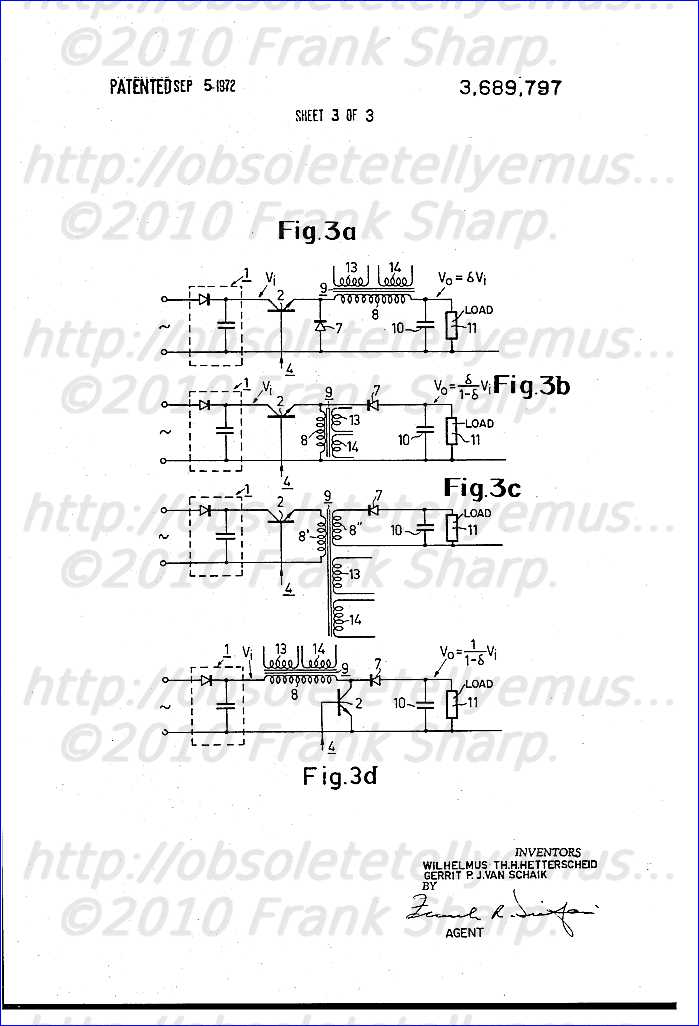 Pulse oscillator 6 applies pulses of line frequency to modulator 5. It may be advantageous to have two line frequency generators as already described, to wit pulse oscillator 6 and line oscillator 6' which is present in the picture display device and which is directly synchronized in known manner by line synchronizing pulses 7'. In fact, in this case line oscillator 6' applies a signal of great amplitude and free from interference to pulse oscillator 6. However, it is alternatively possible to combine pulse oscillator 6 and line oscillator 6' in one single oscillator 6" (see FIG. 1) which results in an economy of components. It will be evident that line oscillator 6' and oscillator 6" may alternatively be synchronized indirectly, for example, by means of a phase discriminator. It is to be noted neither pulse oscillator 6, line oscillator 6' and oscillator 6" nor modulator 5 can be fed by the supply described since output voltage V o is still not present when the mains voltage is switched on. Said circuit arrangements must therefore be fed directly from the input terminals. If as described above these circuit arrangements are to be separated from the mains, a small separation transformer can be used whose primary winding is connected between the mains voltage terminals and whose secondary winding is connected to ground at one end and controls a rectifier at the other end.
Capacitor 27 is arranged parallel to efficiency diode 7 so as to reduce the dissipation in switching transistor 2. In fact, if transistor 2 is switched off by the pulsatory control voltage, its collector current decreases and its collector-emitter voltage increases simultane
ously so that the dissipated power is not negligible before the collector current has becomes zero. If efficiency diode 7 is shunted by capacitor 27 the increase of the collector-emitter voltage is delayed i.e., this voltage does not assume high values until the collector current has already been reduced. It is true that in that case the dissipation in transistor 2 slightly increases when it is switched on by the pulsatory control voltage but on the other hand since the current flowing through diode 7 has decreased due to the presence of the secondary windings, its inverse current is also reduced when transistor 2 is switched on and hence its dissipation has become smaller. In addition it is advantageous to delay these switching-on and switching-off periods to a slight extent because the switching pulses then contain fewer Fourier components of high frequency which may cause interferences in the picture display device and which may give rise to visible interferences on the screen of the display tube. These interferences occupy a fixed position on the displayed image because the switching frequency is the line frequency which is less disturbing to the viewer. In a practical circuit wherein the line frequency is 15,625 Hz and wherein switching transistor 2 is an experimental type suitable for a maximum of 350 V collector-emitter voltage or 1 A collector current and wherein efficiency diode 7 is of the Philips type BA 148 the capacitance of capacitor 27 is approximately 680 pF whilst the load is 70 W on the primary and 20 W on the secondary side of transformer 9. The collector dissipation upon switching off is 0.3 W (2.5 times smaller than without capacitor 27) and 0.7 W upon switching on.As is known the so-called pincushion distortion is produced in the picture display tubes having a substantially flat screen and large deflection angles which are currently used. This distortion is especially a problem in color television wherein a raster correction cannot be brought about by magnetic means. The correction of the so-called East-West pincushion distortion i.e., in the horizontal direction on the screen of the picture display tube can be established in an elegant manner with the aid of the circuit arrangement according to the invention. In fact, if the voltage generated by comparison circuit 12 and being applied to modulator 5 for duration-modulating pulsatory voltage 3 is modulated by a parabola voltage 28 of field frequency, pulsatory voltage 3 is also modulated thereby. If the power consumption of the line deflection circuit forms part of the load on the output voltage of the chopper, the signal applied to the line deflection coils is likewise modulated in the same manner. Conditions therefore are that the parabola voltage 28 of field frequency has a polarity such that the envelope of the sawtooth current of line frequency flowing through the line deflection coils has a maximum in the middle of the scan of the field period and that charge capacitor 10 has not too small an impedance for the field frequency. On the other hand the other supply voltages which are generated by the circuit arrangement according to the invention and which might be hampered by this component of field frequency must be smoothed satisfactorily.
A practical embodiment of the described example with the reference numerals given provides an output for the supply of approximately 85 percent at a total load of 90 W, the internal resistance for direct current loads being 1.5 ohms and for pulsatory currents being approximately 10 ohms. In case of a variation of ± 10 percent of the mains voltage, output voltage V o is stable within 0.4 V. Under the nominal circumstances the collector dissipation of switching transistor 2 is approximately 2.5 W.
Since the internal resistance of the supply is so small, it can be used advantageously, for example, at terminal 15 for supplying a class-B audio amplifier which forms part of the display device. Such an amplifier has the known advantages that its dissipation is directly proportional to the amplitude of the sound to be reproduced and that its output is higher than that of a class-A amplifier. On the other hand a class-A amplifier consumes a substantially constant power so that the internal resistance of the supply voltage source is of little importance. However, if this source is highly resistive, the supply voltage is modulated in the case of a class-B amplifier by the audio information when the sound intensity is great which may detrimentally influence other parts of the display device. This drawback is prevented by means of the supply according to the invention.
The 50 Hz ripple voltage which is superimposed on the rectified input voltage V i is compensated by comparison circuit 12 and modulator 5 since this ripple voltage may be considered to be a variation of input voltage V i . A further compensation is obtained by applying a portion of this ripple voltage with suitable polarity to comparison circuit 12. It is then sufficient to have a lower value for the smoothing capacitor which forms part of rectifier circuit 1 (see FIG. 3). The parabola voltage 28 of field frequency originating from the field time base is applied to the same circuit 12 so as to correct the East-West pincushion distortion.
DA1170 vertical deflection FRAME DEFLECTION INTEGRATED CIRCUIT
GENERAL DESCRIPTION f The TDA1170 and TDA1270 are monolithic integrated
circuits designed for use in TV vertical deflection systems. They are manufactured using
the Fairchild Planar* process.
Both devices are supplied in the 12-pin plastic power package with the heat sink fins bent
for insertion into the printed circuit board.
The TDA1170 is designed primarily for large and small screen black and white TV
receivers and industrial TV monitors. The TDA1270 is designed primarily for driving
complementary vertical deflection output stages in color TV receivers and industrial
monitors.
APPLICATION INFORMATION (TDA1170)
The vertical oscillator is directly synchronized by the sync pulses (positive or negative); therefore its free
running frequency must be lower than the sync frequency. The use of current feedback causes the yoke
current to be independent of yoke resistance variations due to thermal effects, Therefore no thermistor is
required in series with the yoke. The flyback generator applies a voltage, about twice the supply voltage, to
the yoke. This produces a short flyback time together with a high useful power to dissipated power
ratio.
1. A transformerless output vertical deflection circuit, comprising a vertical oscillator circuit for generating a vertical pulse train in response to vertical synchronizing pulses applied thereto, a sawtooth signal generator for generating a series of sawtooth signals, each cycle of said sawtooth signal including a pulse component, a vertical output circuit coupled to said sawtooth generator for amplifying said sawtooth signal including said pulse component and loading a vertical deflection coil, and stabilizing means connected between said vertical oscillator and said sawtooth signal generator for varying the width of the pulse component which is to be fed to said vertical output circuit in response to the average level of DC output voltage fed from the vertical output circuit. 2. A transformerless output vertical deflection circuit claimed in claim 1, wherein said stabilizing means comprises a control circuit means for receiving a series of pulses from the vertical oscillator and a feedback signal from the vertical output circuit and for varying the width of the pulse which is to be fed to the vertical output circuit in response to a DC control signal proportional to the width of the pulse component included in the vertical output signal and smoothing circuit means connected between said vertical output circuit and said stabalizing means for smoothing said feedback signal. 3. A transformerless output vertical deflection circuit claimed in claim 2, wherein said control circuit comprises a charging capacitor which is parallel to a transistor, said transistor being switched on in response to pulses fed from the vertical oscillator wherein said capacitor is charged by the voltage fed from said smoothing circuit, and discharged in response to conduction of the transistor, a differential amplifier circuit which receives the voltage on said capacitor and a fixed voltage, and a gating circuit for producing a pulse which has a width equal to the difference between the width of the pulse fed from the vertical oscillator circuit and the width of pulse fed from the differential amplifier circuit. 4. A transformerless output vertical deflection circuit claimed in claim 2, wherein said control circuit comprises a capacitor which is charged by a fixed power source and is discharged by means of a switching transistor operated by the pulses fed from the vertical oscillator circuit and a differential amplifier circuit receiving the voltage on the capacitor and the output of said smoothing circuit. 5. A transformable output vertical deflection circuit comprising a vertical oscillator for generating a vertical pulse train in response to vertical synchronizing pulses applied thereto, a sawtooth signal generator for generating a series of sawtooth signals each cycle of said sawtooth signal including a pulse component, a vertical output circuit for amplifying said sawtooth signal including said pulse component and loading a vertical deflection coil, and pulse stabilizing means coupled between the vertical oscillator circuit a
Description:
BACKGROUND OF THE INVENTION
The present invention relates to a vertical deflection circuit for use in a television receiver and, more particularly, to a vertical deflection circuit of a type wherein no vertical output transformer is employed. This type of vertical deflection circuit with no output transformer is generally referred to as an OTL (Output Transformerless) type vertical deflection circuit.
It is known that variation of the pulse width of the flyback pulse produced in a vertical output stage of the vertical deflection circuit is the cause in the raster on the television picture tube, of a white bar, flicker, jitter, line crowding and/or other raster disorders. In addition thereto, in the vertical deflection output circuit where the output stage is composed of a single-ended push-pull amplifier having a vertical output transistor, an excessive load is often imposed on the output transistor and, in an extreme case, the output transistor is destroyed.
No comments:
Post a Comment
The most important thing to remember about the Comment Rules is this:
The determination of whether any comment is in compliance is at the sole discretion of this blog’s owner.
Comments on this blog may be blocked or deleted at any time.
Fair people are getting fair reply. Spam and useless crap and filthy comments / scrapers / observations goes all directly to My Private HELL without even appearing in public !!!
The fact that a comment is permitted in no way constitutes an endorsement of any view expressed, fact alleged, or link provided in that comment by the administrator of this site.
This means that there may be a delay between the submission and the eventual appearance of your comment.
Requiring blog comments to obey well-defined rules does not infringe on the free speech of commenters.
Resisting the tide of post-modernity may be difficult, but I will attempt it anyway.
Your choice.........Live or DIE.
That indeed is where your liberty lies.
Note: Only a member of this blog may post a comment.