


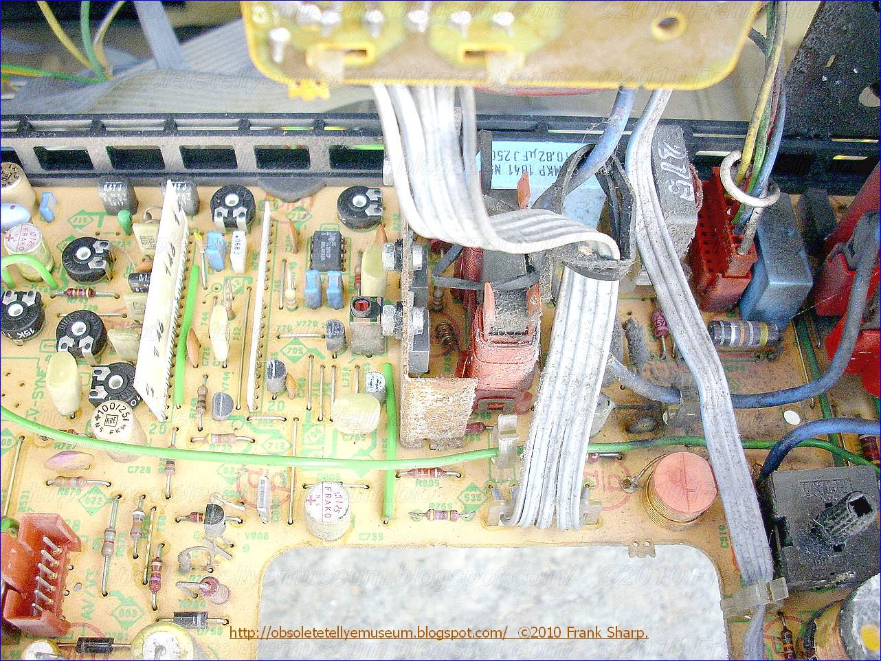


The CHASSIS FM 100-20
 DA was fitted in many models type from BLAUPUNKT and SIEMENS brand types.
The CHASSIS FM 100-20 DA is developed by SIEMENS under joint venture with BOSCH.
This chassis is a complex type and it employs high quality components and it is highly engineered.
You will not find a dry joint on these chassis, soldering are Excellent even after 30 Years.
 Was
highly reliable but the Line output EHT Transformer was failing Very
often causing from defocusing of picture to EHT discarge and even a no
start of the tellye at all.
Was
highly reliable but the Line output EHT Transformer was failing Very
often causing from defocusing of picture to EHT discarge and even a no
start of the tellye at all.Basically the EHT Bleeder output was going "off limits" during aging landing to abnormal or no function at all.
Even the HR-DIEMEN replacement was failing since it was too much an exact replica !!!!!!
Tuning control Unit A Motorola PLL Synthesizer based on ASIC Controller + UAA2000
Even synchronization IC uses Hybrid IC Technology on Ceramic substrate.
And the Frame deflection driving / control circuitry IC uses Hybrid IC Technology on Ceramic substrate.
On a ceramic substrate, spiral-type inductors of a single layer wiring of a metal thin film are provided and respectively connected to a wiring pattern formed on another face of the substrate via through holes. A semiconductor chip is flip-chip mounted on the substrate in a face-down manner. On the face of the semiconductor chip, capacitors composed of a highly dielectric material, resistors formed by an ion implantation method or a thin-film forming method, and FETs are provided, respectively. Interconnection between the substrate and an external circuit board is achieved employing terminals formed at end faces of the substrate. The terminals have a concave shape with respect to the end face of the substrate. Thus, there is no need to use a package, and miniaturization and reduction in cost of a high-performance hybrid IC is achieved.
1. A hybrid IC comprising:
a substrate including a front face, a back face opposite the front face, and side faces interposed between the front face and the back face which define an outer perimeter of the substrate;
at least one inductor formed on at least one of the front face and the back face of the substrate;
a semiconductor chip mounted on the front face of the substrate by flip-chip bonding;
at least one terminal formed in a predetermined portion of the side faces of the substrate,
wherein the semiconductor chip comprises a plurality of circuit elements provided therein, at least one of the plurality of circuit elements being an MIM capacitor having a metal-insulation film-metal (MIM) structure, the insulation film being composed of a highly dielectric material.
2. A hybrid IC according to claim 1 further comprising at least one matching circuit for matching an input signal to the circuit elements provided inside the semiconductor chip, the matching circuit comprising at least one inductor.
3.
A hybrid IC according to claim 2, wherein a wiring pattern is formed of
a single metal layer on both the front and back faces of the substrate,
the wiring patterns on the respective front and back faces of the
substrate being interconnected with each other via through holes, and
the at least one inductor comprised in the matching circuit is formed in
the wiring pattern on one of the respective front and back faces of the
substrate.4. A hybrid IC according to claim 2, wherein the matching circuit is constituted only by inductors and comprises at least one serial inductor and at least one parallel inductor.
5. A hybrid IC according to claim 4, wherein the parallel inductor comprised in the matching circuit is a spiral-type inductor, outermost wiring of the spiral-type inductor being grounded.
6. A hybrid IC according to claim 2, wherein the inductors comprised in the matching circuit are a spiral-type inductor or a meander-type inductor.
7. A hybrid IC according to claim 2, wherein the matching circuit comprises an inductor and a capacitor, the capacitor being formed inside the semiconductor chip.
8. A hybrid IC according to claim 7, wherein the inductor comprised in the matching circuit is a spiral-type inductor or a meander-type inductor.
9. A hybrid IC according to claim 1, wherein the at least one terminal includes at least an RF terminal functioning as an input terminal for an RF signal, an LO terminal functioning as an input terminal for an LO signal, an IF terminal functioning as an output terminal for an IF signal, a ground terminal, and a supply terminal.
---------------------------------------
- VIDEO CHROMA PROCESSING WITH TDA3300 (MOTOROLA)

TDA3300 3301 TV COLOR PROCESSOR
This device will accept a PAL or NTSC composite video signal and output the
three color signals, needing only a simple driver amplifier to interface to the pic-
ture tube. The provision of high bandwidth on-screen display inputs makes it
suitable for text display, TV games, cameras, etc. The TDA3301 B has user con»
trol laws, and also a phase shift control which operates in PAL, as well as NTSC.
0 Automatic Black Level Setup
0 Beam Current Limiting
0 Uses Inexpensive 4.43 MHZ to 3.58 MHz Crystal
0 No Oscillator Adjustment Required
0 Three OSD Inputs Plus Fast Blanking Input
0 Four DC, High Impedance User Controls
0 lnterlaces with TDA33030B SECAM Adaptor
0 Single 12 V Supply
0 Low Dissipation, Typically 600 mW
The brilliance control operates by adding a pedestal to the output
signals. The amplitude of the pedestal is controlled by Pin 30.
During CRT beam current sampling a standard pedestal is
substituted, its value being equivalent tothe value given by V30 Nom
currents at the sampling level, i.e. 3x20 |.1A with 100 k reference
resistors on Pins 16, 19, and 22.
During picture blanking the brilliance pedestal is zero; therefore, the
output voltage during blanking is always the minimum brilliance black
level (Note: Signal channels are also gain blanked).
Chrominance Decoder
The chrominance decoder section of the TDA3301 B
consists of the following blocks:
Phase-locked reference oscillator;
Phase-locked 90 degree servo loop;
U and V axis decoders
ACC detector and identification detector; .
Identification circuits and PAL bistable; .
Color difference filters and matrixes with fast blanking
Circuits.
The major design considerations apart from optimum
performance were:
o A minimum number of factory adjustments,
o A minimum number of external components,
0 Compatibility with SECAM adapter TDA3030B,
0 Low dissipation,
0 Use of a standard 4.433618 Mhz crystal rather
than a 2.0 fc crystal with a divider.
The crystal VCO is of the phase shift variety in which thefrequency is controlled by varying the phase of the feedback.
A great deal of care was taken to ensure that the oscillator loop
gain and the crystal loading impedance were held constant in
order to ensure that the circuit functions well with low grade
crystal (crystals having high magnitude spurious responses
can cause bad phase jitter). lt is also necessary to ensure that
the gain at third harmonic is low enough to ensure absence of
oscillation at this frequency.
It can be seen that the
necessary 1 45°C phase shift is obtained by variable addition
ol two currents I1 and I2 which are then fed into the load
resistance of the crystal tuned circuit R1. Feedback is taken
from the crystal load capacitance which gives a voltage of VF
lagging the crystal current by 90°.
The RC network in the T1 collector causes I1 to lag the
collector current of T1 by 45°.
For SECAM operation, the currents I1 and I2 are added
together in a fixed ratio giving a frequency close to nominal.
When decoding PAL there are two departures from normal
chroma reference regeneration practice:
a) The loop is locked to the burst entering from the PAL
delay line matrix U channel and hence there is no
alternating component. A small improvement in signalnoise ratio is gained but more important is that the loop
filter is not compromised by the 7.8 kHz component
normally required at this point for PAL identification
b) The H/2 switching of the oscillator phase is carried out
before the phase detector. This implies any error signal
from the phase detector is a signal at 7.8 kHz and not dc.
A commutator at the phase detector output also driven
from the PAL bistable coverts this ac signal to a dc prior
to the loop filter. The purpose ot this is that constant
offsets in the phase detector are converted by the
commutator to a signal at 7.8 kHz which is integrated to
zero and does not give a phase error.
When used for decoding NTSC the bistable is inhibited, and
slightly less accurate phasing is achieved; however, as a hue
control is used on NTSC this cannot be considered to be a
serious disadvantage.
90° Reference Generation
To generate the U axis reference a variable all-pass network
is utilized in a servo loop. The output of the all-pass network
is compared with the oscillator output with a phase detector of
which the output is filtered and corrects the operating point of
the variable all»pass network .
As with the reference loop the oscillator signal is taken after
the H/2 phase switch and a commutator inserted before the
filter so that constant phase detector errors are cancelled.
For SECAM operation the loop filter is grounded causing
near zero phase shift so that the two synchronous detectors
work in phase and not in quadralure.
The use of a 4.4 MHz oscillator and a servo loop to generate
the required 90° reference signal allows the use of a standard,
high volume, low cost crystal and gives an extremely accurate90° which may be easily switched to 0° for decoding AM
SECAM generated by the TDA3030B adapter.
ACC and Identification Detectors
During burst gate time the output components of the U and
also the V demodulators are steered into PNP emitters. One
collector current of each PNP pair is mirrored and balanced
against its twin giving push-pull current sources for driving the
ACC and the identification filter capacitors.
The identification detector is given an internal offset by
making the NPN current mirror emitter resistors unequal. The
resistors are offset by 5% such that the identification detector
pulls up on its filter capacitor with zero signal.
Identification
See Figure 11 for definitions.
Monochrome I1 > I2
PAL ldent. OK I1 < lg
PAL ldent_ X l1 > I2
NTSC I3 > I2
Only for correctly identified PAL signal is the capacitor
voltage held low since I2 is then greater than I1.
For monochrome and incorrectly identified PAL signals l1>l2
hence voltage VC rises with each burst gate pulse.
When V,ef1 is exceeded by 0.7 V Latch 1 is made to conduct
which increases the rate of voltage rise on C. Maximum
current is limited by R1.
When Vref2 is exceeded by 0.7 V then Latch 2 is made to
conduct until C is completely discharged and the current drops
to a value insufficient to hold on Latch 2.
As Latch 2 turns on Latch 1 must turn off.
Latch 2 turning on gives extra trigger pulse to bistable to
correct identification.
The inhibit line on Latch 2 restricts its conduction to alternate
lines as controlled by the bistable. This function allows the
SECAM switching line to inhibit the bistable operation by firing
Latch 2 in the correct phase for SECAM. For NTSC, Latch 2
is fired by a current injected on Pin 6.
lf the voltage on C is greater than 1.4 V, then the saturation
is held down. Only for SECAM/NTSC with Latch 2 on, or
correctly identified PAL, can the saturation control be
anywhere but minimum.
NTSC Switch
NTSC operation is selected when current (I3) is injected into
Pin 6. On the TDA33O1 B this current must be derived
externally by connecting Pin 6 to +12 V via a 27 k resistor (as
on TDA33OOB). For normal PAL operation Pin 40 should be
connected to +12 V and Pin 6 to the filter capacitor.
4 Color Difference Matrixing, Color Killing,
and Chroma BlankingDuring picture time the two demodulators feed simple RC
filters with emitter follower outputs. Color killing and blanking
is performed by lifting these outputs to a voltage above the
maximum value that the color difference signal could supply.
The color difference matrixing is performed by two
differential amplifiers, each with one side split to give the
correct values of the -(B-Y) and -(Ft-Y) signals. These are
added to give the (G-Y) signal.
The three color difference signals are then taken to the
virtual grounds of the video output stages together with
luminance signal.
Sandcastle Selection
The TDA3301B may be used with a two level sandcastle
and a separate frame pulse to Pin 28, or with only a three level
(super) sandcastle. In the latter case, a resistor of 1.0 MQ is
necessary from + 12 V to Pin 28 and a 70 pF capacitor from
Pin 28 to ground.
Timing Counter for Sample Control
In order to control beam current sampling at the beginning
of each frame scan, two edge triggered flip-flops are used.
The output K ofthe first flip-flop A is used to clock the second
tlip-flop B. Clocking of A by the burst gate is inhibited by a count
of A.B.
The count sequence can only be initiated by the trailing
edge of the frame pulse. ln order to provide control signals for:
Luma/Chroma blanking
Beam current sampling
On-screen display blanking
Brilliance control
The appropriate flip-flop outputs ar matrixed with sandcastle
 and frame signals by an emitter-follower matrix.
Video Output Sections
Each video output stage consists of a feedback amplifier in A further drive current is used to control the DC operating
which the input signal is a current drive to the virtual earth from point; this is derived from the sample and hold stage which
the luminance, color difference and on-screen display stages. samples the beam current after frame flyback.
CHASSIS FM100-20CA SMPS POWER Supply is based on TDA4600 (SIEMENS).
BLAUPUNKT VERONA ID39 COLOR (7 660 370) CHASSIS FM100-20DA Power supply Description based on TDA4601d (SIEMENS)


 is proportional to chopper drive. In an overload condition it reaches 4v amplitude at which point chopper drive is reduced to a mark-space ratio of 13 to 1, the chip is then in over current trip. The I.C. can easily withstand a short circuit on the H.T. rail and in such a case the power supply simply squegs quietly. Pin 4 is protected by internal protection components which limit the maximum voltage at this pin to 6.5v. Should a fault occur in either of the time constant components, then the chopper transistor will probably be destroyed. Pin 5 This pin can be used for remote control on/off switching of the power supply, it is normally held at about +7v and will cause the chip to enter standby mode if it falls below 2v. Pin 6 Ground. Pin 7 Chopper switch off pin. This pin clamps the chopper drive voltage to 1.6v in order to switch off the chopper. Pin 8 Chopper base current output drive pin. Pin 9 L.T. pin, approximately 9v under start-up conditions and 16v during normal running, Current consumption of the I.C. is typically 135mA. The voltage at this pin must reach 6.7v in order for the chip to start-up.Semiconductor
circuit for supplying power to electrical equipment, comprising a
transformer having a primary winding connected, via a parallel
connection of a collector-emitter path of a transistor with a first
capacitor, to both outputs of a rectifier circuit supplied, in turn, by a
line a-c voltage; said transistor having a base controlled via a second
capacitor by an output of a control circuit acted upon, in turn by the
rectified a-c line voltage as actual value and by a reference voltage;
said transformer having a first secondary winding to which the
electrical equipment to be supplied is connected; said transformer
having a second secondary winding with one terminal thereof connected to
the emitter of said transistor and the other terminal thereof connected
to an anode of a first diode leading to said control circuit; said
transformer having a third secondary winding with one terminal thereof
connected, on the one hand, via a series connection of a third capacitor
with a first resistance, to the other terminal of said third secondary
winding and connected, on the other hand, to the emitter of said
transistor, the collector of which is connected to said primary winding;
a point between said third capacitor and said first resistance being
connected to the cathode of a second diode; said control circuit having
nine terminals including a first terminal delivering a reference voltage
and connected, via a voltage divider formed of a third and fourth
series-connected resistances, to the anode of said second diode; a
second terminal of said control circuit serving for zero-crossing
identification being connected via a fifth resistance to said cathode of
said second diode; a third terminal of said control-circuit serving as
actual value input being directly connected to a divider point of said
voltage divider forming said connection of said first terminal of said
control circuit to said anode of said second diode; a fourth terminal of
said control circuit delivering a sawtooth voltage being connected via a
sixth resistance to a terminal of said primary winding of said
transformer facing away from said transistor; a fifth terminal of said
control circuit serving as a protective input being connected, via a
seventh resistance to the cathode of said first diode and, through the
intermediary of said seventh resistance and an eighth resistance, to the
cathode of a third diode having an anode connected to an input of said
rectifier circuit; a sixth terminal of said control circuit carrying
said reference potential and being connected via a fourth capacitor to
said fourth terminal of said control circuit and via a fifth capacitor
to the anode of said second diode; a seventh terminal
of said control circuit establishing a potential for pulses controlling
said transistor being connected directly and an eighth terminal of said
control circuit effecting pulse control of the base of said transistor
being connected through the intermediary of a ninth resistance to said
first capacitor leading to the base of said transistor; and a ninth
terminal of said control circuit serving as a power supply input of said
control circuit being connected both to the cathode of said first diode
as well as via the intermediary of a sixth capacitor to a terminal of
said second secondary winding as well as to a terminal of said third
secondary winding.
is proportional to chopper drive. In an overload condition it reaches 4v amplitude at which point chopper drive is reduced to a mark-space ratio of 13 to 1, the chip is then in over current trip. The I.C. can easily withstand a short circuit on the H.T. rail and in such a case the power supply simply squegs quietly. Pin 4 is protected by internal protection components which limit the maximum voltage at this pin to 6.5v. Should a fault occur in either of the time constant components, then the chopper transistor will probably be destroyed. Pin 5 This pin can be used for remote control on/off switching of the power supply, it is normally held at about +7v and will cause the chip to enter standby mode if it falls below 2v. Pin 6 Ground. Pin 7 Chopper switch off pin. This pin clamps the chopper drive voltage to 1.6v in order to switch off the chopper. Pin 8 Chopper base current output drive pin. Pin 9 L.T. pin, approximately 9v under start-up conditions and 16v during normal running, Current consumption of the I.C. is typically 135mA. The voltage at this pin must reach 6.7v in order for the chip to start-up.Semiconductor
circuit for supplying power to electrical equipment, comprising a
transformer having a primary winding connected, via a parallel
connection of a collector-emitter path of a transistor with a first
capacitor, to both outputs of a rectifier circuit supplied, in turn, by a
line a-c voltage; said transistor having a base controlled via a second
capacitor by an output of a control circuit acted upon, in turn by the
rectified a-c line voltage as actual value and by a reference voltage;
said transformer having a first secondary winding to which the
electrical equipment to be supplied is connected; said transformer
having a second secondary winding with one terminal thereof connected to
the emitter of said transistor and the other terminal thereof connected
to an anode of a first diode leading to said control circuit; said
transformer having a third secondary winding with one terminal thereof
connected, on the one hand, via a series connection of a third capacitor
with a first resistance, to the other terminal of said third secondary
winding and connected, on the other hand, to the emitter of said
transistor, the collector of which is connected to said primary winding;
a point between said third capacitor and said first resistance being
connected to the cathode of a second diode; said control circuit having
nine terminals including a first terminal delivering a reference voltage
and connected, via a voltage divider formed of a third and fourth
series-connected resistances, to the anode of said second diode; a
second terminal of said control circuit serving for zero-crossing
identification being connected via a fifth resistance to said cathode of
said second diode; a third terminal of said control-circuit serving as
actual value input being directly connected to a divider point of said
voltage divider forming said connection of said first terminal of said
control circuit to said anode of said second diode; a fourth terminal of
said control circuit delivering a sawtooth voltage being connected via a
sixth resistance to a terminal of said primary winding of said
transformer facing away from said transistor; a fifth terminal of said
control circuit serving as a protective input being connected, via a
seventh resistance to the cathode of said first diode and, through the
intermediary of said seventh resistance and an eighth resistance, to the
cathode of a third diode having an anode connected to an input of said
rectifier circuit; a sixth terminal of said control circuit carrying
said reference potential and being connected via a fourth capacitor to
said fourth terminal of said control circuit and via a fifth capacitor
to the anode of said second diode; a seventh terminal
of said control circuit establishing a potential for pulses controlling
said transistor being connected directly and an eighth terminal of said
control circuit effecting pulse control of the base of said transistor
being connected through the intermediary of a ninth resistance to said
first capacitor leading to the base of said transistor; and a ninth
terminal of said control circuit serving as a power supply input of said
control circuit being connected both to the cathode of said first diode
as well as via the intermediary of a sixth capacitor to a terminal of
said second secondary winding as well as to a terminal of said third
secondary winding.Description:
The
invention relates to a blocking oscillator type switching power supply
for supplying power to electrical equipment, wherein the primary winding
of a transformer, in series with the emitter-collector path of a first
bipolar transistor, is connected to a d-c voltage obtained by
rectification of a line a-c voltage fed-in via two external supply
terminals, and a secondary winding of the transformer is provided for
supplying power to the electrical equipment, wherein, furthermore, the
first bipolar transistor has a base controlled by the output of a
control circuit which is acted upon in turn by the rectified a-c line
voltage as actual value and by a set-point transmitter, and wherein a
starting circuit for further control of the base of the first bipolar
transistor is provided. Such a blocking oscillator switching power supply is described in the German periodical, "Funkschau" (1975) No. 5, pages 40 to 44. It is well known that the purpose of such a circuit is to supply electronic equipment, for example, a television set, with stabilized and controlled supply voltages. Essential for such switching power supply is a power switching transistor i.e. a bipolar transistor with high switching speed and high reverse v
oltage. This
transistor therefore constitutes an important component of the control
element of the control circuit. Furthermore, a high operating frequency
and a transformer intended for a high operating frequency are provided,
because generally, a thorough separation of the equipment to be supplied
from the supply naturally is desired. Such switching power supplies may
be constructed either for synchronized or externally controlled
operation or for non-synchronized or free-running operation. A blocking
converter is understood to be a switching power supply in which power is
delivered to the equipment to be supplied only if the switching
transistor establishing the connection between the primary coil of the
transformer and the rectified a-c voltage is cut off. The power
delivered by the line rectifier to the primary coil of the transformer
while the switching transistor is open, is interim-stored in the
transformer and then delivered to the consumer on the secondary side of
the transformer with the switching transistor cut off. In the blocking converter described in the aforementioned reference in the literature, "Funkschau" (1975), No. 5, Pages 40 to 44, the power switching transistor is connected in the manner defined in the introduction to this application. In addition, a so-called starting circuit is provided. Because several diodes are generally provided in the overall circuit of a blocking oscillator according to the definition provided in the introduction hereto, it is necessary, in order not to damage these diodes, that due to the collector peak current in the case of a short circuit, no excessive stress of these diodes and possibly existing further sensitive circuit parts can occur.
Considering
the operation of a blocking oscillator, this means that, in the event of
a short circuit, the number of collector current pulses per unit time
must be reduced. For this purpose, a control and regulating circuit is provided.
Simultaneously, a starting circuit must bring the blocking converter
back to normal operation when the equipment is switched on, and after
disturbances, for example, in the event of a short circuit. The starting
circuit shown in the literature reference "Funkschau" on Page 42
thereof, differs to some extent already from the conventional d-c
starting circuits. It is commonly known for all heretofore known
blocking oscillator circuits, however, that a thyristor or an equivalent
circuit replacing the thyristor is essential for the operation of the
control circuit. It is accordingly an object of the invention to provide another starting circuit. It is a further object of the invention to provide a possible circuit for the control circuit which is particularly well suited for this purpose. It is yet another object of the invention to provide such a power supply which is assured of operation over the entire range of line voltages from 90 to 270 V a-c, while the secondary voltages and secondary load variations between no-load and short circuit are largely constant.
With the foregoing and other objects in view, there is
provided, in accordance with the invention, a blocking oscillator-type
switching power supply for supplying power to electrical equipment
wherein a primary winding of a transformer, in series with an
emitter-collector path of a first bipolar transistor, is connected to a
d-c voltage obtained by rectification of a line a-c voltage fed-in via
two external supply terminals, a secondary winding of the transformer
being connectible to the electrical equipment for supplying power
thereto, the first bipolar transistor having a base controlled by the
output of a control circuit acted upon, in turn, by the rectified a-c
line voltage as actual value and by a set-point transmitter, and
including a starting circuit for further control of the base of the
first bipolar transistor, including a first diode in the starting
circuit having an anode directly connected to one of the supply
terminals supplied by the a-c line voltage and a cathode connected via a
resistor to an input serving to supply power to the control circuit,
the input being directly connected to a cathode of a second diode, the
second diode having an anode connected to one terminal of another
secondary winding of the transformer, the other secondary winding having
another terminal connected to the emitter of the first bipolar
transmitter. In
accordance with another feature of the invention, there is provided a
second bipolar transistor having the same conduction type as that of the
first bipolar transistor and connected in the starting circuit with the
base thereof connected to a cathode of a semiconductor diode, the
semiconductor diode having an anode connected to the emitter of the
first bipolar transistor, the second bipolar transistor having a
collector connected via a resistor to a cathode of the first diode in
the starting circuit, and having an emitter connected to the input
serving to supply power to the control circuit and also connected to the
cathode of the second diode which is connected to the other secondary
winding of the transformer. In accordance with a further feature of the invention, the base of the second bipolar transistor is connected to a resistor and via the latter to one pole of a first capacitor, the anode of the first diode being connected to the other pole of the first capacitor.
In accordance with an added feature of the invention, the input serving to supply power to the control circuit is connected via a second capacitor to an output of a line rectifier, the output of the line rectifier being directly connected to the emitter of the first bipolar transistor.
In accordance with an additional feature of the invention, the other secondary winding is connected at one end to the emitter of the first bipolar transistor and to a pole of a third capacitor, the third capacitor having another pole connected, on the one hand, via a resistor, to the other end of the other secondary winding and, on the other hand, to a cathode of a third diode, the third diode having an anode connected via a potentiometer to an actual value input of the control circuit and, via a fourth capacitor, to the emitter of the first bipolar transistor.
In accordance with yet another feature of the invention, the control circuit has a control output connected via a fifth capacitor to the base of the first bipolar transistor for conducting to the latter control pulses generated in the control circuit.
In accordance with a concomitant feature of the invention, there is provided a sixth capacitor shunting the emitter-collector path of the first transistor.
Other features which are considered as characteristic for the invention are set forth in the appended claim.
 Although
the invention is illustrated and described herein as embodied in a
blocking oscillator type switching power supply, it is nevertheless not
intended to be limited to the details shown, since various modifications
and structural changes may be made therein without departing from the
spirit of the invention and within the scope and range of equivalents of
the claims.
Although
the invention is illustrated and described herein as embodied in a
blocking oscillator type switching power supply, it is nevertheless not
intended to be limited to the details shown, since various modifications
and structural changes may be made therein without departing from the
spirit of the invention and within the scope and range of equivalents of
the claims. The construction and method of operation of the invention, however, together with additional objects and advantages thereof will be best understood from the following description of specific embodiments when read in connection with the accompanying drawings, in which:
FIGS. 1 and 2 are circuit diagrams of the blocking oscillator type switching power supply according to the invention; and
FIG. 3 is a circuit diagram of the control unit RS of FIGS. 1 and 2.
Referring now to the drawing and, first, particularly to FIG. 1 thereof, there is shown a rectifier circuit G in the form of a bridge current, which is acted upon by a line input represented by two supply terminals 1' and 2'. Rectifier outputs 3' and 4' are shunted by an emitter-collector path of an NPN power transistor T1 i.e. t
 he
series connection of the so-called first bipolar transistor referred to
hereinbefore with a primary winding I of a transformer Tr. Together
with the inductance of the transformer Tr, the capacitance C1 determines
the frequency and limits the opening voltages of the switch embodied by
the first transistor T1. A capacitance C2, provided between the base of
the first transistor T1 and the control output 7,8 of a control circuit
RS, separates the d-c potentials of the control or regulating circuit
RS and the switching transistor T1 and serves for addressing this
switching transistor T1 with pulses. A resistor R1 provided at the
control output 7,8 of the control circuit RS is the negative-feedback
resistor of both output stages of the control circuit RS. It determines
the maximally possible output pulse current of the control circuit RS. A
secondary winding II of the transformer Tr takes over the power supply
of the control circuit, in steady state operation, via the diode D1. To
this end, the cathode of this diode D1 is directly connected to a power
supply input 9 of the control circuit RS, while the anode thereof is
connected to one terminal of the secondary winding II. The other
terminal of the secondary winding II is connected to the emitter of the
power switching transistor T1.
he
series connection of the so-called first bipolar transistor referred to
hereinbefore with a primary winding I of a transformer Tr. Together
with the inductance of the transformer Tr, the capacitance C1 determines
the frequency and limits the opening voltages of the switch embodied by
the first transistor T1. A capacitance C2, provided between the base of
the first transistor T1 and the control output 7,8 of a control circuit
RS, separates the d-c potentials of the control or regulating circuit
RS and the switching transistor T1 and serves for addressing this
switching transistor T1 with pulses. A resistor R1 provided at the
control output 7,8 of the control circuit RS is the negative-feedback
resistor of both output stages of the control circuit RS. It determines
the maximally possible output pulse current of the control circuit RS. A
secondary winding II of the transformer Tr takes over the power supply
of the control circuit, in steady state operation, via the diode D1. To
this end, the cathode of this diode D1 is directly connected to a power
supply input 9 of the control circuit RS, while the anode thereof is
connected to one terminal of the secondary winding II. The other
terminal of the secondary winding II is connected to the emitter of the
power switching transistor T1.The cathode of the diode D1 and, therewith, the power supply terminal 9 of the control circuits RS are furthermore connected to one pole of a capacitor C3, the other pole of which is connected to the output 3' of the rectifier G. The capacitance of this capacitor C3 thereby smoothes the positive half-wave pulses and serves simultaneously as an energy storage device during the starting period. Another secondary windi
 ng
III of the transformer Tr is connected by one of the leads thereof
likewise to the emitter of the first transistor T1, and by the other
lead thereof via a resistor R2, to one of the poles of a further
capacitor C4, the other pole of which is connected to the
first-mentioned lead of the other secondary winding III. This second
pole of the capacitor C4 is simultaneously connected to the output 3' of
the rectifier circuit G and, thereby, via the capacitor C3, to the
cathode of the diode D1 driven by the secondary winding II of the
transformer Tr as well as to the power supply input 9 of the control
circuit RS and, via a resistor R9, to the cathode of a second diode D4.
The second pole of the capacitor C4 is simultaneously connected directly
to the terminal 6 of the control circuit RS and, via a further
capacitor C 6, to the terminal 4 of the control circuit RS as well as,
additionally, via the resistor R6, to the other output 4' of the
rectifier circuit G. The other of the poles of the capacitor C4 acted
upon by the secondary winding II is connected via a further capacitor C5
to a node, which is connected on one side thereof, via a variable
resistor R4, to the terminals 1 and 3 of the control circuit RS, with
the intermediary of a fixed resistor R5 in the case of the terminal 1.
On the other side of the node, the latter and, therefore, the capacitor
C5 are connected to the anode of a third diode D2, the cathode of which
is connected on the one hand, to the resistor R2 mentioned hereinbefore
and leads to the secondary winding III of the transformer Tr and, on the
other hand, via a resistor R3 to the terminal 2 of the control circuit
RS.
ng
III of the transformer Tr is connected by one of the leads thereof
likewise to the emitter of the first transistor T1, and by the other
lead thereof via a resistor R2, to one of the poles of a further
capacitor C4, the other pole of which is connected to the
first-mentioned lead of the other secondary winding III. This second
pole of the capacitor C4 is simultaneously connected to the output 3' of
the rectifier circuit G and, thereby, via the capacitor C3, to the
cathode of the diode D1 driven by the secondary winding II of the
transformer Tr as well as to the power supply input 9 of the control
circuit RS and, via a resistor R9, to the cathode of a second diode D4.
The second pole of the capacitor C4 is simultaneously connected directly
to the terminal 6 of the control circuit RS and, via a further
capacitor C 6, to the terminal 4 of the control circuit RS as well as,
additionally, via the resistor R6, to the other output 4' of the
rectifier circuit G. The other of the poles of the capacitor C4 acted
upon by the secondary winding II is connected via a further capacitor C5
to a node, which is connected on one side thereof, via a variable
resistor R4, to the terminals 1 and 3 of the control circuit RS, with
the intermediary of a fixed resistor R5 in the case of the terminal 1.
On the other side of the node, the latter and, therefore, the capacitor
C5 are connected to the anode of a third diode D2, the cathode of which
is connected on the one hand, to the resistor R2 mentioned hereinbefore
and leads to the secondary winding III of the transformer Tr and, on the
other hand, via a resistor R3 to the terminal 2 of the control circuit
RS.The nine terminals of the control circuit RS have the following purposes or functions:
Terminal 1 supplies the internally generated reference voltage to ground i.e. the nominal or reference value required for the control or regulating process;
Terminal 2 serves as input for the oscillations provided by the secondary winding III, at the zero point of which, the pulse start of the driving pulse takes place;
Terminal 3 is the control input, at which the existing actual value is communicated to the control circuit RS, that actual value being generated by the rectified oscillations at the secondary winding III;
Terminal 4 is responsive to the occurrence of a maximum excursion i.e. when the largest current flows through the first transistor T1 ;
Terminal 5 is a protective input which responds if the rectified line voltage drops too sharply; Terminal 6 serves for the power supply of the control process and, indeed, as ground terminal;
Terminal 7 supplies the d-c component required for charging the coupling capacitor C2 leading to the base of the first transistor T1 ;
Terminal 8 supplies the control pulse required for the base of the first transistor T1 ; and
Terminal 9 serves as the first terminal of the power supply of the control circuit RS.
Further details of the control circuit RS are described hereinbelow.
The capacity C3 smoothes the positive half-wave pulses which are provided by the secondary winding II, and simultaneously serves as an energy storage device during the starting time. The secondary winding III generates the control voltage and is simultaneously used
 as
feedback. The time delay stage R2 /C4 keeps harmonics and fast
interference spikes away from the control circuit RS. The resistor R3 is
provided as a voltage divider for the second terminal of the control
circuit RS. The diode D2 rectifies the control pulses delivered by the
secondary winding III. The capacity C5 smoothes the control voltage. A
reference voltage Uref, which is referred to ground i.e. the potential
of terminal 6 is present at the terminal 1 of the control circuit RS.
The resistors R4 and R5 form a voltage divider of the input-difference
control amplifier at the terminal 3. The desired secondary voltage can
be set manually via the variable resistor R4. A time-delay stage R6 /C6
forms a sawtooth rise which corresponds to the collector current rise of
the first bipolar transistor T1 via the primary winding I of the
transformer Tr. The sawtooth present at the terminal 4 of the control
circuit RS is limited there between the reference voltage 2 V and 4 V.
The voltage divider R7 /R8 (FIG. 2), brings to the terminal 5 of the
control circuit RS the enabling voltage for the drive pulse at the
output 8 of the control circuit RS.
as
feedback. The time delay stage R2 /C4 keeps harmonics and fast
interference spikes away from the control circuit RS. The resistor R3 is
provided as a voltage divider for the second terminal of the control
circuit RS. The diode D2 rectifies the control pulses delivered by the
secondary winding III. The capacity C5 smoothes the control voltage. A
reference voltage Uref, which is referred to ground i.e. the potential
of terminal 6 is present at the terminal 1 of the control circuit RS.
The resistors R4 and R5 form a voltage divider of the input-difference
control amplifier at the terminal 3. The desired secondary voltage can
be set manually via the variable resistor R4. A time-delay stage R6 /C6
forms a sawtooth rise which corresponds to the collector current rise of
the first bipolar transistor T1 via the primary winding I of the
transformer Tr. The sawtooth present at the terminal 4 of the control
circuit RS is limited there between the reference voltage 2 V and 4 V.
The voltage divider R7 /R8 (FIG. 2), brings to the terminal 5 of the
control circuit RS the enabling voltage for the drive pulse at the
output 8 of the control circuit RS.The diode D4, together with the resistor R9 in cooperation with the diode D1 and the secondary winding II, forms the starting circuit provided, in accordance with the invention. The operation thereof is as follows:
After the switching power supply is switched on, d-c voltages build up at the collector of the switching transistor T1 and at the input 4 of the control circuit RS, as a function in time of the predetermined time constants. The positive sinusoidal half-waves charge the capacitor C3 via the starting diode D4 and the starting resistor R9 in dependence upon the time constant R9.C3. Via the protective input terminal 5 and the resisto
r
R11 not previously mentioned and forming the connection between the
resistor R9 and the diode D1, on the one hand, and the terminal 5 of the
control circuit RS, on the other hand, the control circuit RS is biased
ready for switching-on, and the capacitor C2 is charged via the output
7. When a predetermined voltage value at the capacitor C3 or the power
supply input 9 of the control circuit RS, respectively, is reached, the
reference voltage i.e. the nominal value for the operation of the
control voltage RS, is abruptly formed, which supplies all stages of the
control circuit and appears at the output 1 thereof. Simultaneously,
the switching transistor T1 is switched into conduction via the output
8. The switching of the transistor T1 at the primary winding T of the
transformer Tr is transformed to the second secondary winding II, the
capacity C3 being thereby charged up again via the diode D1. If
sufficient energy is stored in the capacitor C3 and if the re-charge via
the diode D1 is sufficient so that the voltage at a supply input 9 does
not fall below the given minimum operating voltage, the switching power
supply then remains connected, so that the starting process is
completed. Otherwise, the starting process described is repeated several
times.In FIG. 2, there is shown a further embodiment of the circuit for a blocking oscillator type switching power supply, according to the invention, as shown in FIG. 1. Essential for this circuit of FIG. 2 is the presence of a second bipolar transistor T2 of the type of the first bipolar transistor T1 (i.e. in the embodiments of the invention, an npn-transistor), which forms a further component of the starting circuit and is connected with the collector-emitter path thereof between the resistor R9 of the starting circuit and the current supply input 9 of the control circuit RS. The base of this second transistor T2 is connected to a node which leads, on the one hand, via a resistor R10 to one electrode of a capacitor C7, the other electrode of which is connected to the anode of the diode D4 of the starting circuit and, accordingl
y,
to the terminal 1' of the supply input of the switching power supply G.
On the other hand, the last-mentioned node and, therefore, the base of
the second transistor T2 are connected to the cathode of a Zener diode
D3, the anode of which is connected to the output 3' of the rectifier G
and, whereby, to one pole of the capacitor C3, the second pole of which
is connected to the power supply input 9 of the control circuit RS as
well as to the cathode of the diode D1 and to the emitter of the second
transistor T2. In other respects, the circuit according to FIG. 2
corresponds to the circuit according to FIG. 1 except for the resistor
R11 which is not necessary in the embodiment of FIG. 2, and the missing
connection between the resistor R9 and the cathode of the diode D1,
respectively, and the protective input 5 of the control circuit RS.Regarding the operation of the starting circuit according to FIG. 2,
 it can be stated that the positive sinusoidal half-wave of the line
voltage, delayed by the time delay stage C7, R10 drives the base of the
transistor T2 in the starting circuit. The amplitude is limited by the
diode D3 which is provided for overvoltage protection of the control
circuit RS and which is preferably incorporated as a Zener diode. The
second transistor T2 is switched into conduction. The capacity C3 is
charged, via the serially connected diode D4 and the resistor R9 and the
collector-emitter path of the transistor T2, as soon as the voltage
between the terminal 9 and the terminal 6 of the control circuit RS i.e.
the voltage U9, meets the condition U9 <[UDs -UBE (T2)].
it can be stated that the positive sinusoidal half-wave of the line
voltage, delayed by the time delay stage C7, R10 drives the base of the
transistor T2 in the starting circuit. The amplitude is limited by the
diode D3 which is provided for overvoltage protection of the control
circuit RS and which is preferably incorporated as a Zener diode. The
second transistor T2 is switched into conduction. The capacity C3 is
charged, via the serially connected diode D4 and the resistor R9 and the
collector-emitter path of the transistor T2, as soon as the voltage
between the terminal 9 and the terminal 6 of the control circuit RS i.e.
the voltage U9, meets the condition U9 <[UDs -UBE (T2)].Because of the time constant R9.C3, several positive half-waves are necessary in order to increase the voltage U9 at the supply terminal 9 of the control circuit RS to such an extent that the control circuit RS is energized. During the negative sine half-wave, a partial energy chargeback takes place from the capacitor C3 via the emitter-base path of the transistor T2 of the starting circuit and via the resistor R10 and the capacitor C7, respectively, into the supply network. At approximately 2/3 of the voltage U9, which is limited by the diode D3, the control circuit RS is switched on. At the terminal 1 thereof, the reference voltage Uref then appears. In addition, the voltage divider R5 /R4 becomes effective. At the terminal 3, the control amplifier receives the voltage forming the actual value, while the first bipolar transistor T1 of the blocking-oscillator type switching power supply is addressed pulsewise via the terminal 8.
Because the capacitor C6 is charged via the resistor R6, a higher voltage than Uref is present at the terminal 4 if the control circuit RS is activated. The control voltage then discharges the capacitor C6 via the terminal 4 to half the value of the reference voltage Uref, and immediately cuts off the addressing input 8 of the control circuit RS. The first driving pulse of the switching transistor T1 is thereby limited to a minimum of time. The power for switching-on the control circuit RS and for driving the transistor T1 is supplied by the capacitor C3. The voltage U9 at the capacitor C3 then drops. If the voltage U9 drops below the switching-off voltage value of the control circuit RS, the latter is then inactivated. The next positive sine half-wave would initiate the starting process again.
By switching the transistor T1, a voltage is transformed in the secondary winding II of the transformer Tr. The positive component is rectified by the diode D1, recharing of the capacitor C3 being thereby provided. The voltage U9 at the output 9 does not, therefore, drop below the minimum value required for the operation of the control circuit RS, so that the control circuit RS remains activated. The power supply continues to operate in the rhythm of the existing conditions. In operation, the voltage U9 at the supply terminal 9 of the control circuit RS has a value which meets the condition U9 >[UDs -UBE (T2)], so that the transistor T2 of the starting circuit remains cut off.
For the internal layout of the control circuit RS, the construction shown, in particular, from FIG. 3 is advisable. This construction is realized, for example, in the commercially available type TDA 4600 (Siemens AG).
The block diagram of the control circuit according to FIG. 3
 shows
the power supply thereof via the terminal 9, the output stage being
supplied directly whereas all other stages are supplied via Uref. In the
starting circuit, the individual subassemblies are supplied with power
sequentially. The d-c output voltage potential of the base current gain
i.e. the voltage for the terminal 8 of the control circuit RS, and the
charging of the capacitor C2 via the terminal 7 are formed even before
the reference voltage Uref appears. Variations of the supply voltage U9
at terminal 9 and the power fluctuations at the terminal 8/terminal 7
and at the terminal 1 of the control circuit RS are leveled or smoothed
out by the voltage control. The temperature sensitivity of the control
circuit RS and, in particular, the uneven heating of the output and
input stages and input stages on the semiconductor chip containing the
control circuit in monolithically integrated form are intercepted by the
temperature compensation provided. The output values are constant in a
specific temperature range. The message for blocking the output stage,
if the supply voltage at the terminal 9 is too low, is given also by
this subassembly to a provided control logic.
shows
the power supply thereof via the terminal 9, the output stage being
supplied directly whereas all other stages are supplied via Uref. In the
starting circuit, the individual subassemblies are supplied with power
sequentially. The d-c output voltage potential of the base current gain
i.e. the voltage for the terminal 8 of the control circuit RS, and the
charging of the capacitor C2 via the terminal 7 are formed even before
the reference voltage Uref appears. Variations of the supply voltage U9
at terminal 9 and the power fluctuations at the terminal 8/terminal 7
and at the terminal 1 of the control circuit RS are leveled or smoothed
out by the voltage control. The temperature sensitivity of the control
circuit RS and, in particular, the uneven heating of the output and
input stages and input stages on the semiconductor chip containing the
control circuit in monolithically integrated form are intercepted by the
temperature compensation provided. The output values are constant in a
specific temperature range. The message for blocking the output stage,
if the supply voltage at the terminal 9 is too low, is given also by
this subassembly to a provided control logic.The outer voltage divider of the terminal 1 via the r
 esistors
R5 and R4 to the control tap U forms, via terminal 3, the variable side
of the bridge for the control amplifier formed as a differential
amplifier. The fixed bridge side is formed by the reference voltage Uref
via an internal voltage divider. Similarly formed are circuit portions
serving for the detection of an overload short circuit and circuit
portions serving for the "standby" no-load detection, which can be
operated likewise via terminal 3.
esistors
R5 and R4 to the control tap U forms, via terminal 3, the variable side
of the bridge for the control amplifier formed as a differential
amplifier. The fixed bridge side is formed by the reference voltage Uref
via an internal voltage divider. Similarly formed are circuit portions
serving for the detection of an overload short circuit and circuit
portions serving for the "standby" no-load detection, which can be
operated likewise via terminal 3.Within a provided trigger circuit, the driving pulse length is determined as a function of the sawtooth rise at the terminal 4, and is transmitted to the control logic. In the control logic, the commands of the trigger circuit are processed. Through the zero-crossing identification at input 2 in the control circuit RS, the control logic is enabled to start the control input only at the zero point of the frequency oscillation. If the voltages at the terminal 5 and at the terminal 9 are too low, the control logic blocks the output amplifier at the terminal 8. The output amplifier at the terminal 7 which is responsible for the base charge in the capacitor C2, is not touched thereby.
The base current gain for the transistor T1 i.e. for the first transistor in accordance with the definition of the invention, is formed by two amplifiers which mutually operate on the capacitor C2. The roof inclination of the base driving current for the transistor T1 is impressed by the collector current simulation at the terminal 4 to the amplifier at the terminal 8. The control pulse for the transistor T1 at the terminal 8 is always built up to the potential present at the terminal 7. The amplifier working into the terminal 7 ensures that each new switching pulse at the terminal 8 finds the required base level at terminal 7.
Supplementing the comments regarding FIG. 1, it should also be mentioned that the cathode of the diode D1 connected by the anode thereof to the one end of the secondary winding II of the transformer Tr is connected via a resistor R11 to the protective input 5 of the control circuit RS whereas, in the circuit according to FIG. 2, the protective input 5 of the control circuit RS is supplied via a voltage divider R8, R7 directly from the output 3', 4' of the rectifier G delivering the rectified line a-c voltage, and which obtains the voltage required for executing its function. It is evident that the first possible manner of driving the protective input 5 can be used also in the circuit according to FIG. 2, and the second possibility also in a circuit in accordance with FIG. 1.
The control circuit RS which is shown in FIG. 3 and is realized in detail by the building block TDA 4600 and which is particularly well suited in conjunction with the blocking oscillator type switching power supply according to the invention has 9 terminals 1-9, which have the following characteristics, as has been explained in essence hereinabove:
Terminal 1 delivers a reference voltage Uref which serves as the constant-current source of a voltage divider R5.R4 which supplies the required d-c voltages for the differential amplifiers provided for the functions control, overload detection, short-circuit detection and "standby"-no load detection. The dividing point of the voltage divider R5 -R4 is connected to the terminal 3 of the control circuit RS. The terminal 3 provided as the control input of RS is controlled in the manner described hereinabove as input for the actual value of the voltage to be controlled or regulated by the secondary winding III of the transformer Tr. With this input, the lengths of the control pulses for the switching transistor T1 are determined.
Via the input provided by the terminal 2 of the control circuit RS, the zero-point identification in the control circuit is addressed for detecting the zero-point o
f
the oscillations respectively applied to the terminal 2. If this
oscillation changes over to the positive part, then the addressing pulse
controlling the switching transistor T1 via the terminal 8 is released
in the control logic provided in the control circuit.A sawtooth-shaped voltage, the rise of which corresponds to the collector current of the switching transistor T1, is present at the terminal 4 and is minimally and maximally limited by two reference voltages. The sawtooth voltage serves, on the one hand as a comparator for the pulse length while, on the other hand, the slope or rise thereof is used to obtain in the base current amplification for the switching transistor T1, via the terminal 8, a base drive of this switching transistor T1 which is proportional to the collector current.
The terminal 7 of the control circuit RS as explained hereinbefore, determines the voltage potential for the addressing pulses of the transistor T2. The base of the switching transistor T1 is pulse-controlled via the terminal 8, as described hereinbefore. Terminal 9 is connected as the power supply input of the control circuit RS. If a voltage level falls below a given value, the terminal 8 is blocked. If a given positive value of the voltage level is exceeded, the control circuit is activated. The terminal 5 releases the terminal 8 only if a given voltage potential is present.
Forei
gn References:DE2417628A1 1975-10-23 363/37
DE2638225A1 1978-03-02 363/49
Other References:
Grundig Tech. Info. (Germany), vol. 28, No. 4, (1981).
IBM Technical Disclosure Bulletin, vol. 19, No. 3, pp. 978, 979, Aug. 1976.
German Periodical, "Funkschau", (1975), No. 5, pp. 40 to 44.
Inventors:
Peruth, Gunther (Munich, DE) Siemens Aktiengesellschaft (Berlin and Munich, DE)The CHASSIS FM 100-20 CA delivers a totally uncommon Frame deflection system, derived from previous chassis types. (YEARS 1978)
Plus the E/W Correection circuit uses the same Technology.
It's a system called S.S.V.D. which stays for Synchronized Switched Vertical Deflection.
The system is highly reliable and does dissipate energy like linear amplifier types like A class or AB class Types and should not be confused with D Class amplifier.
Abstract:
In
a switched vertical deflection circuit, two SCR switches couple
horizontal retrace pulses to a capacitor. A modulator couples pulse
width modulated gating pulses to the SCR's. The SCR's couple
to the capacitor successively smaller portions of the horizontal
retrace pulses during a first part of the vertical trace interval and
successively larger portions during a second part for developing in a
vertical deflection winding a sawtooth vertical deflection current. The
modulator couples gating pulses to one of the SCR's during the vertical
retrace interval for substantially loading the horizontal deflection
circuit during the vertical retrace interval for preventing undesired
oscillations within the horizontal deflection circuit.
What is claimed is:
1. A switched vertical deflection system comprising:a horizontal deflection circuit including first means for generating horizontal rate energy signals;
a vertical deflection winding;
energy storage capacitance means coupled to said vertical deflection winding;
first and second switching means coupled to said first means and said energy storage capacitance means; and
second means coupled to said first and second switching means for switching conductive states of both of said switching means for coupling successively smaller portions of said horizontal rate energy signals to said energy storage capacitancemeans during a first part of a vertical trace interval and successively larger portions of said horizontal rate energy signals during a second part of said vertical trace interval for developing a vertical deflection current in said vertical deflectionwinding during said vertical trace interval,
said second means causing said first switching means to conduct during a vertical retrace interval for coupling substantial portions of said horizontal rate energy signals to said energy storage capacitance means during said vertical retraceinterval for preventing undesired oscillations within said horizontal deflection circuit.
2.
A system according to claim 1 wherein said first and second switching
means comprise controlled semiconductors, said second means coupling
first and second signals to said first and second switching means for
switching conductive states ofboth of said controlled semiconductors.3. A system according to claim 2 wherein said second means includes transformer means for coupling said first signals to said first switching means.
4. A system according to claim 3 wherein said first switching means comprises a silicon controlled rectifier, a secondary winding of said transformer means coupled between the gate and cathode electrodes of said silicon controlled rectifier.
5. A system according to claim 2 including vertical signal means coupled to said second means for generating a vertical rate signal for modulating said first and second signals at a vertical rate.
6. A system according to claim 5 wherein said vertical signal means includes first circuitry for generating a component of said vertical rate signal that inhibits conduction of said second switching means during said vertical retrace interval.
7. A system according to claim 6 wherein said first circuitry comprises an RC differentiating circuit.
8. A system according to claim 7 wherein the time constant of said differentiating circuit is selected to provide a duration for said component of said vertical rate signal substantially equal to said vertical retrace interval.
9. In a television receiver including a horizontal deflection circuit comprising a horizontal deflection generator and a horizontal output transformer, a switched vertical deflection circuit comprising:
a vertical deflection winding;
energy storage capacitance means coupled to said vertical deflection winding;
first and second controllable switches coupled to said capacitance means and to respective secondary windings of said horizontal output transformer for coupling horizontal retrace signals to said capacitance means; and
a
modulator coupled to said first and second controllable switches and
responsive to a source of vertical rate signals for providing to said
controllable switches during said vertical trace interval horizontal
rate signals
modulated at a verticalrate for varying the amount of each horizontal
retrace signal coupled to said capacitance means for generating a
vertical deflection current in said vertical deflection winding during
said vertical trace interval, said switched vertical deflectioncircuit
substantially loading said horizontal deflection circuit at the
beginning and end of said vertical trace interval,said modulator providing signals to said first controllable switch during said vertical retrace interval for coupling said horizontal retrace signals to said capacitance means during said vertical retrace interval for substantially loading saidhorizontal deflection circuit during said retrace interval for preventing undesired oscillations within said horizontal deflection circuit.
10. A circuit according to claim 9 wherein said vertical rate signals cause said modulator to provide for conduction of said first controllable switch during said vertical retrace interval and for inhibiting conduction of said second controllable swith during said vertical retrace interval.
Description:
BACKGROUND OF THE INVENTION
This invention relates to switched vertical deflection circuits for a television receiver.
In
a switched vertical deflection circuit of the type disclosed in U.S.
Patent Application Ser. No. 595,809, now U.S. Pat. No. 4,048,544, filed
July 11, 1975, by Peter Eduard Haferl, entitled, SWITCHED VERTICAL
DEFLECTION SYSTEM, horizontalrate energy, in the form of horizontal
retrace pulses from a horizontal output transformer of a horizontal
deflection circuit, charges a capacitor in parallel with a vertical
deflection winding. A first switch, such as an SCR, couples
successivelysmaller portions of the horizontal rate energy to the
capacitor during a first part of the vertical trace interval and a
second switch, such as another SCR, couples successively larger portions
of the horizontal rate energy during a second part of thevertical trace
interval. The voltage across the capacitor is integrated by the
vertical deflection winding into a sawtooth vertical deflection current.
The conduction of the two SCR switches is controlled by horizontal rate
pulse width modulated pulsescoupled from a modulator to the SCR gate
electrodes.
At the start of  vertical
retrace, the second SCR switch which had previously been conducting is
maintained in cutoff. The vertical deflection winding and the capacitor
form a resonant retrace circuit. A disconnect diode coupled to the gate
ofthe first SCR switch is reversed biased, maintaining the SCR in cutoff
independent of the gating pulses generated by the modulator. With both
SCR's nonconducting, resonant retrace of the current in the vertical
deflection winding is accomplished. Atthe start of the subsequent
vertical trace interval, the disconnect diode is no longer reverse
biased. Pulse width modulated gating pulses to the first SCR enable the
SCR to couple the horizontal retrace pulses to the capacitor for
generating thesawtooth deflection current in the vertical deflection
winding.
vertical
retrace, the second SCR switch which had previously been conducting is
maintained in cutoff. The vertical deflection winding and the capacitor
form a resonant retrace circuit. A disconnect diode coupled to the gate
ofthe first SCR switch is reversed biased, maintaining the SCR in cutoff
independent of the gating pulses generated by the modulator. With both
SCR's nonconducting, resonant retrace of the current in the vertical
deflection winding is accomplished. Atthe start of the subsequent
vertical trace interval, the disconnect diode is no longer reverse
biased. Pulse width modulated gating pulses to the first SCR enable the
SCR to couple the horizontal retrace pulses to the capacitor for
generating thesawtooth deflection current in the vertical deflection
winding.
Both SCR's
conduct relatively large amounts of current at the beginning and end of
the vertical trace interval, respectively. Neither SCR conducts during
the vertical retrace interval. Accordingly, loading of the horizontal
deflection circuitby the switched vertical deflection circuit will be
greatest at the beginning and end of the vertical trace interval, with
substantially no loading occurring during the vertical retrace interval.
Such load interruption during the vertical retraceinterval may cause
undesirable modulation of the horizontal deflection current and
undesirable oscillations within the horizontal deflection circuit. These
oscillations may appear, for example, in the "S" shaping capacitor or
in the horizontal outputtransformer windings as the load impedance of
the vertical deflection circuit abruptly changes. It is, therefore,
desirable to provide a switched vertical deflection circuit in which
undesirable oscillations within the horizontal deflection circuit
areprevented.
SUMMARY OF THE INVENTION
A
switched vertical deflection circuit comprises a horizontal deflection
circuit including apparatus for generating horizontal rate energy
signals, a vertical deflection winding, an energy storage capacitance,
first and second switches and aswitching circuit coupled to the
switches. The switching circuit switches the conductive states of the
switches for coupling successively smaller portions of the horizontal
rate energy signals to the energy storage capacitance during a first
part of thevertical trace interval and successively larger portions
during a second part for developing a vertical deflection current in the
vertical deflection winding during the vertical trace interval. The
switching circuit causes the first switch to conductduring the vertical
retrace interval for coupling substantial portions of the horizontal
rate energy signals to the energy storage capacitance during the
vertical retrace interval for preventing undesired oscillations within
the horizontal deflection circuit.
To permit use of a circuit in which the energy derived during horizontal flyback is used to control ve
rtical
deflection, without damage to the vertical deflection system upon
vertical flyback, the vertical deflection output stage is dimensioned to
have a time constant which is less, preferably about half, of the time
constant of the sawtooth wave generator controlling vertical deflection.
The vertical deflection output stage forms, in essence, a parallel
oscillatory circuit which, to provide the lesser time constant, is
damped.1. In a television receiver,
having means (1, 2) coupling out a portion of the energy delivered by the horizontal deflection circuit during line flyback or retrace;
a vertical deflection output stage (V) including deflection means (LV1, LV2) and a charge capacitor element (C);
and a sawtooth wave generator (S), which controls application of the coupled-out energy derived from the horizontal deflection circuit to the vertical deflection means (LV1, LV2), a method to control vertical deflection
comprising, in accordance with the invention, the step of
additionally controlling application of the energy to the vertical deflection means by the sawtooth wave generator during the vertical flyback or retrace interval by reversely re-charging said capacitor element during said interval.
2. Method according to claim 1, wherein the re-charging step is carried out continuously.
3. Method according to claim 1, wherein the re-charging step is carried out linearly.
4. Method accordi
 ng to claim 1, wherein the vertical deflection output stage includes, vertical deflection coil elements (LV1, LV2)
and forming with said charge capacitor element (C) said deflection
means, a feedback resistor element (R) and a vertical correction circuit
element (4), said charge capacitor element and said other elements
being connected to form a parallel oscillatory circuit;
ng to claim 1, wherein the vertical deflection output stage includes, vertical deflection coil elements (LV1, LV2)
and forming with said charge capacitor element (C) said deflection
means, a feedback resistor element (R) and a vertical correction circuit
element (4), said charge capacitor element and said other elements
being connected to form a parallel oscillatory circuit; said method including the step of controlling the damping of the parallel oscillatory circuit by controlling the relative parameters of said elements.
5. In a television receiver, a vertical deflection system including means (1, 2) coupling out a portion of the energy delivered by the horizontal deflection circuit during line flyback or retrace;
a vertical deflection output stage (V) including vertical deflection means (LV1, LV2);
and a sawtooth wave generator (S) controlling application of the coupled-out energy to the vertical deflection means during the flyback interval
and wherein, in accordance with the invention,
the time constant (τS) of the sawtooth wave generator (S) is longer than the time constant (τV) of the vertical deflection output stage (V).
6. Vertical deflection system
according to claim 5, wherein the time constant of the vertical
deflection output stage is about twice as long as that of the sawtooth
wave generator (S).7. Vertical deflection system according to claim 5, wherein the ratio of time constants (τS /τV) is between about 1.5 to 2.5.
8. Vertical deflection system according to claim 5, wherein the vertical deflection output stage (V) includes a charge capacitor element (C), vertical deflection coil elements (LV1, LV2) forming said vertical deflection means, a feedback resistor element (R) and a vertical correction circuit element (4), said elements being connected to form a parallel oscillatory circuit;
and wherein said oscillatory circuit is a damped oscillatory circuit.
9. Vertical deflection system according to claim 8, wherein the elements of said oscillatory circuit are dimensioned to provide a time constant which is about half of the time constant of the sawtooth wave generator (S) and is in the order of about 0.5 ms.
Description:
The
present invention relates to a deflection circuitry for television
receivers, and more particularly to a deflection circuit in which energy
contained in the horizontal flyback is used in the vertical deflection
system.
Video scanning in television receivers is effected, as well known, by a vertical deflection circuit. A pulse generator is synchronized by pulses included in the video signal. The pulses are then applied over a pulse generator, a driver and an output stage to deflection systems, usually deflection coils.
Various types of solid-state circuits have been proposed; for example, U.S. Pat. No. 4,048,544 describes a transistorized vertical deflection circuit with additional circuitry to stabilize the pulses. The time constant of the pulse generator and of the driver stage of such circuits is less than the time constant of the output or final power stage of the vertical
deflection circuit. Such vertical deflection circuits have some
disadvantages, particularly in that the transistors are operated at high
voltages which may result in flash-over and thus damage or destruction
of the transistor. The power required to control the final output
transistors is already substantial and thus the overall operating
efficiency of such a vertical deflection circuit is low.
the time constant of the output or final power stage of the vertical
deflection circuit. Such vertical deflection circuits have some
disadvantages, particularly in that the transistors are operated at high
voltages which may result in flash-over and thus damage or destruction
of the transistor. The power required to control the final output
transistors is already substantial and thus the overall operating
efficiency of such a vertical deflection circuit is low.
In earlier developments, a vertical deflection circuitry was proposed which avoids some of the disadvantages of this transistorized circuit; in this earlier circuit, a portion of the energy contained in the horizontal flyback is coupled out and is directly utilized in order to supply current for the vertical deflection coils. To control application of current, a controlled sawtooth wave generator is connected to the final output stage of the vertical deflection circuit, the sawtooth wave generator having a short retrace or flyback time. These vertical deflection circuits also have some disadvantages. The energy derived for vertical deflection is obtained from the horizontal flyback; thus, changes in loading in the vertical deflection circuitry affect the horizontal output stage. The vertical deflection circuit is subject to substantial changes in loading during the vertical flyback or retrace since, in accordance with the previously known circuit, the vertical deflection circuit is not controlled during the vertical flyback or retrace. The lack of control of the vertical deflection circuit causes abrupt changes in loading which result in undesired spurious oscillations in the vertical output stage. These oscillations can so feed back or react on the horizontal output stage that the horizontal flyback pulses are overloaded, the vertical stage starts to oscillate, and high voltages may occur therein during the vertical flyback. This, necessarily, degrades the image quality of the reproduced video picture. High-voltage flash-over may occur and electronic components, particularly solid-state semiconductor elements can be destroyed thereby.
It is an object of the present invention to provide a vertical deflection circuit for television receivers, which has the advantages of utilizing a portion of the energy contained in the horizontal deflection circuit during horizontal flyback without causing abrupt changes in loading on the horizontal output stage and preventing undesired spurious and uncontrolled oscillation of the vertical output stage.
SUBJECT MATTER OF THE PRESENT INVENTION
Briefly, the sawtooth wave generator which controls charging of a charge capacitor of the vertical output stage is controlled to in turn control the charge on the capacitor also during vertical retrace; in accordance with a feature of the invention, this control is obtained by so arranging and relatively matching the time constants of the sawtooth wave generator and of the parallel oscillatory circuit formed by the vertical deflection coils of the T.V. receiver and the charge capacitor that the time constant of the vertical deflection output stage is less, preferably about half that of the time constant of the sawtooth wave generator. This matching can be obtained by so selecting the values of the components of the vertical deflection output stage that the resulting oscillatory circuit formed by the capacitor, resistance elements in the circuit, and the vertical deflection output stage form a damped oscillatory circuit.
The invention will be described by way of example with reference to the accompanying drawings, wherein the single FIGURE is a schematic diagram of a vertical deflection output stage in which the method of the present invention is carried out, and utilizing the system thereof.
 A horizontal deflection output stage 1 is connected to a horizontal output transformer 2 which has coupling windings W 1 and W 2 to derive a portion of the energy contained in the line retrace. This energy is stored in the inductances L 1 and L 2 and then applied through thyristors Th 1 and Th 2 to a charge capacitor C. A control circuit 3 is provided triggering the thyristors Th 1 and Th 2
in such a manner that the charge capacitor C is positively charged
during the first half of the video scan and negatively during the second
half of the video scan. The charge capacitor C is discharged through
the vertical deflection coils L V1 and L V2 , a
vertical correction circuit 4 for vertical correction and a feedback
resistor R. The voltage drop across feedback resistor R is fed back to
the control circuit 3 in order to ensure exact triggering of the
thyristors Th 1 and Th 2 and to control the desired deflection current.
A horizontal deflection output stage 1 is connected to a horizontal output transformer 2 which has coupling windings W 1 and W 2 to derive a portion of the energy contained in the line retrace. This energy is stored in the inductances L 1 and L 2 and then applied through thyristors Th 1 and Th 2 to a charge capacitor C. A control circuit 3 is provided triggering the thyristors Th 1 and Th 2
in such a manner that the charge capacitor C is positively charged
during the first half of the video scan and negatively during the second
half of the video scan. The charge capacitor C is discharged through
the vertical deflection coils L V1 and L V2 , a
vertical correction circuit 4 for vertical correction and a feedback
resistor R. The voltage drop across feedback resistor R is fed back to
the control circuit 3 in order to ensure exact triggering of the
thyristors Th 1 and Th 2 and to control the desired deflection current.
Positive deflection current is obtained during the first half of the video scan by the triggered thyristor Th 1 ; negative deflection current is derived during the second half of the video scan by the triggered thyristor Th 2 . The thyristors Th 1 and Th 2 can be triggered during a portion of the video scan simultaneously to result in a linear deflection and provide overlapping, opposite deflection currents.
The control circuit 3, together with the thyristors Th 1 and Th 2 , and the inductances L 1 and L 2 , forms a sawtooth wave generator S. The vertical deflection output stage V is formed of the vertical deflection coils L V1 , L V2 ,
the vertical correction circuit 4, the charge capacitor C and the
feedback resistor R. As can be seen from the FIGURE, the capacitor C on
the one hand, and the deflection coils, the correction circuit 4 and the
resistor R on the other hand form a parallel oscillatory circuit.
coils L V1 , L V2 ,
the vertical correction circuit 4, the charge capacitor C and the
feedback resistor R. As can be seen from the FIGURE, the capacitor C on
the one hand, and the deflection coils, the correction circuit 4 and the
resistor R on the other hand form a parallel oscillatory circuit.
The circuit, as far as the diagram is concerned, is known. Uncontrolled, undesired and spurious oscillations in the horizontal output stage can be avoided, in accordance with the invention, by reverse re-charging the capacitor C also during the vertical retrace interval. This re-charging of the capacitor C preferably is carried out continuously and desirably linearly. The controlled re-charging of the capacitor C can be readily obtained by arranging the relative values of the components in the sawtooth wave generator S and in the vertical output stage V such that the time constant τ S of the sawtooth wave generator is longer than the time constant τ V of the vertical deflection output stage. Mathematically: τ S >τ V (1)
preferably, the quotient of the time constants should be between 1.5 and 2.5, most desirably about 2, mathematically: 1.5>τ S /τ V <2.5 (2)
if the time constants of the respective circuits are properly arranged, the thyristors Th 1 and Th 2 can be precisely triggered also during the short time interval of the vertical flyback or retrace. Due to the short time constant, the vertical deflection circuit can then follow the control from the control circuit 3 exactly; the voltage dropped across the feedback resistor R will permit precise triggering, with respect to time, of the thyristors Th 1 and Th 2 also during the vertical flyback. In the first half of the video scan, the thyristor Th 2 is triggered; in the second half, thyristor Th 1 is triggered. This ensures linear flyback.
The time constant τ V is essentially determined by the vertical deflection coils L V1 , L V2 , the correction circuit 4, and the feedback resistor R which, together with the capacitor C, form a parallel oscillatory circuit. A short time constant corresponds to high damping of this parallel oscillatory circuit. Thus, in accordance with a feature of the present invention, by suitably arranging the ratio of the time constants, the parallel oscillatory circuit will not start undesired uncontrolled oscillations which could interfere with image reproduction quality, or proper operation of the components of the T.V. receiver. The ratio of the time constants can be selected by suitable adjustment of the damping of the oscillatory circuit.
The vertical deflection circuit has an essentially continuous, uniform and even power requirement. This avoids abrupt changes in loading during the vertical retrace. Excessive over-compensation of horizontal flyback pulses, and resulting high voltages which may lead to undesired distortion of the reproduced image and possibly to damage or destruction of components of the video system are avoided. The vertical deflection circuitry, as described, can be readily manufactured and has high operating reliability. The efficiency is high and the power requirement is low.
Various changes and modifications may be made within the scope of the inventive concept.
In a typical T.V. receiver using vertical deflection coils of 20 millihenry inductance, a suitable time constant τ V
is 0.5 ms. In such a circuit, the resistor R can have a value 1 Ω
capacitor C a value of 1.5 μF. and the reflected impedance of correction
circuit 4 a value of 1 Ω.
The sawtooth wave generator has a time constant of 1 ms, providing for a slow rise time for 20 milliseconds. The circuit 3 is well known and described in U.S. Pat. No. 4,048,544.
Video scanning in television receivers is effected, as well known, by a vertical deflection circuit. A pulse generator is synchronized by pulses included in the video signal. The pulses are then applied over a pulse generator, a driver and an output stage to deflection systems, usually deflection coils.
Various types of solid-state circuits have been proposed; for example, U.S. Pat. No. 4,048,544 describes a transistorized vertical deflection circuit with additional circuitry to stabilize the pulses. The time constant of the pulse generator and of the driver stage of such circuits is less than
the time constant of the output or final power stage of the vertical
deflection circuit. Such vertical deflection circuits have some
disadvantages, particularly in that the transistors are operated at high
voltages which may result in flash-over and thus damage or destruction
of the transistor. The power required to control the final output
transistors is already substantial and thus the overall operating
efficiency of such a vertical deflection circuit is low. In earlier developments, a vertical deflection circuitry was proposed which avoids some of the disadvantages of this transistorized circuit; in this earlier circuit, a portion of the energy contained in the horizontal flyback is coupled out and is directly utilized in order to supply current for the vertical deflection coils. To control application of current, a controlled sawtooth wave generator is connected to the final output stage of the vertical deflection circuit, the sawtooth wave generator having a short retrace or flyback time. These vertical deflection circuits also have some disadvantages. The energy derived for vertical deflection is obtained from the horizontal flyback; thus, changes in loading in the vertical deflection circuitry affect the horizontal output stage. The vertical deflection circuit is subject to substantial changes in loading during the vertical flyback or retrace since, in accordance with the previously known circuit, the vertical deflection circuit is not controlled during the vertical flyback or retrace. The lack of control of the vertical deflection circuit causes abrupt changes in loading which result in undesired spurious oscillations in the vertical output stage. These oscillations can so feed back or react on the horizontal output stage that the horizontal flyback pulses are overloaded, the vertical stage starts to oscillate, and high voltages may occur therein during the vertical flyback. This, necessarily, degrades the image quality of the reproduced video picture. High-voltage flash-over may occur and electronic components, particularly solid-state semiconductor elements can be destroyed thereby.
It is an object of the present invention to provide a vertical deflection circuit for television receivers, which has the advantages of utilizing a portion of the energy contained in the horizontal deflection circuit during horizontal flyback without causing abrupt changes in loading on the horizontal out
put stage and preventing undesired spurious and uncontrolled oscillation of the vertical output stage. SUBJECT MATTER OF THE PRESENT INVENTION
Briefly, the sawtooth wave generator which controls charging of a charge capacitor of the vertical output stage is controlled to in turn control the charge on the capacitor also during vertical retrace; in accordance with a feature of the invention, this control is obtained by so arranging and relatively matching the time constants of the sawtooth wave generator and of the parallel oscillatory circuit formed by the vertical deflection coils of the T.V. receiver and the charge capacitor that the time constant of the vertical deflection output stage is less, preferably about half that of the time constant of the sawtooth wave generator. This matching can be obtained by so selecting the values of the components of the vertical deflection output stage that the resulting oscillatory circuit formed by the capacitor, resistance elements in the circuit, and the vertical deflection output stage form a damped oscillatory circuit.
The invention will be described by way of example with reference to the accompanying drawings, wherein the single FIGURE is a schematic diagram of a vertical deflection output stage in which the method of the present invention is carried out, and utilizing the system thereof.
A horizontal deflection output stage 1 is connected to a horizontal output transformer 2 which has coupling windings W 1 and W 2 to derive a portion of the energy contained in the line retrace. This energy is stored in the inductances L 1 and L 2 and then applied through thyristors Th 1 and Th 2 to a charge capacitor C. A control circuit 3 is provided triggering the thyristors Th 1 and Th 2
in such a manner that the charge capacitor C is positively charged
during the first half of the video scan and negatively during the second
half of the video scan. The charge capacitor C is discharged through
the vertical deflection coils L V1 and L V2 , a
vertical correction circuit 4 for vertical correction and a feedback
resistor R. The voltage drop across feedback resistor R is fed back to
the control circuit 3 in order to ensure exact triggering of the
thyristors Th 1 and Th 2 and to control the desired deflection current. Positive deflection current is obtained during the first half of the video scan by the triggered thyristor Th 1 ; negative deflection current is derived during the second half of the video scan by the triggered thyristor Th 2 . The thyristors Th 1 and Th 2 can be triggered during a portion of the video scan simultaneously to result in a linear deflection and provide overlapping, opposite deflection currents.
The control circuit 3, together with the thyristors Th 1 and Th 2 , and the inductances L 1 and L 2 , forms a sawtooth wave generator S. The vertical deflection output stage V is formed of the vertical deflection
coils L V1 , L V2 ,
the vertical correction circuit 4, the charge capacitor C and the
feedback resistor R. As can be seen from the FIGURE, the capacitor C on
the one hand, and the deflection coils, the correction circuit 4 and the
resistor R on the other hand form a parallel oscillatory circuit. The circuit, as far as the diagram is concerned, is known. Uncontrolled, undesired and spurious oscillations in the horizontal output stage can be avoided, in accordance with the invention, by reverse re-charging the capacitor C also during the vertical retrace interval. This re-charging of the capacitor C preferably is carried out continuously and desirably linearly. The controlled re-charging of the capacitor C can be readily obtained by arranging the relative values of the components in the sawtooth wave generator S and in the vertical output stage V such that the time constant τ S of the sawtooth wave generator is longer than the time constant τ V of the vertical deflection output stage. Mathematically: τ S >τ V (1)
preferably, the quotient of the time constants should be between 1.5 and 2.5, most desirably about 2, mathematically: 1.5>τ S /τ V <2.5 (2)
if the time constants of the respective circuits are properly arranged, the thyristors Th 1 and Th 2 can be precisely triggered also during the short time interval of the vertical flyback or retrace. Due to the short time constant, the vertical deflection circuit can then follow the control from the control circuit 3 exactly; the voltage dropped across the feedback resistor R will permit precise triggering, with respect to time, of the thyristors Th 1 and Th 2 also during the vertical flyback. In the first half of the video scan, the thyristor Th 2 is triggered; in the second half, thyristor Th 1 is triggered. This ensures linear flyback.
The time constant τ V is essentially determined by the vertical deflection coils L V1 , L V2 , the correction circuit 4, and the feedback resistor R which, together with the capacitor C, form a parallel oscillatory circuit. A short time constant corresponds to high damping of this parallel oscillatory circuit. Thus, in accordance with a feature of the present invention, by suitably arranging the ratio of the time constants, the parallel oscillatory circuit will not start undesired uncontrolled oscillations which could interfere with image reproduction quality, or proper operation of the components of the T.V. receiver. The ratio of the time constants can be selected by suitable adjustment of the damping of the oscillatory circuit.
The vertical deflection circuit has an essentially continuous, uniform and even power requirement. This avoids abrupt changes in loading during the vertical retrace. Excessive over-compensation of horizontal flyback pulses, and resulting high voltages which may lead to undesired distortion of the reproduced image and possibly to damage or destruction of components of the video system are avoided. The vertical deflection circuitry, as described, can be readily manufactured and has high operating reliability. The efficiency is high and the power requirement is low.
Various changes and modifications may be made within the scope of the inventive concept.
In a typical T.V. receiver using vertical deflection coils of 20 millihenry inductance, a suitable time constant τ V
is 0.5 ms. In such a circuit, the resistor R can have a value 1 Ω
capacitor C a value of 1.5 μF. and the reflected impedance of correction
circuit 4 a value of 1 Ω. The sawtooth wave generator has a time constant of 1 ms, providing for a slow rise time for 20 milliseconds. The circuit 3 is well known and described in U.S. Pat. No. 4,048,544.
CHASSIS FM100-20DA BLAUPUNKT SSVD E/W CORRECTION Pincushion correction circuitA side pincushion correction circuit having an impedance circuit in series with the deflection coil. A controlled switch coupled
in a branch of the impedance circuit is operated at times during the
second half of the horizontal retrace interval which are progressively
advanced during the first half of vertical interval and retarded
during second half of vertical interval. Enhanced inside pincushion
distortion correction is provided when the impedance circuit includes a
capacitor coupled in series with the switch.1. A pincushion correction circuit for a kinescope deflection apparatus including horizontal and vertical deflection generator systems, comprising:
a horizontal deflection winding coupled to the horizontal deflection generator system for accepting scanning current therefrom;
an impedance circuit for presenting an impedance between first and second terminals and further including a third terminal, and first coupling means for coupling said first terminal to said third terminal;
second means for serially coupling said first and second terminals of said impedance circuit with said deflection windin
g; controllable switch means including a control electrode and a controlled current path coupled between said second and third terminals;
control means coupled to the horizontal and vertical deflection generator systems and to said control electrode for operating said controllable switch means at a time during the second half of the horizontal retrace interval which time is progressively advanced during a first portion of the vertical scan interval and which is progressively retarded during a second portion of the vertical scan interval for altering said scanning current in a manner to reduce pincushion distortion.
2. A pincushion correction circuit in accordance with claim 1 wherein said first coupling means comprises a direct connection.
3. A pincushion correction circuit in accordance with claim 1 wherein said impedance circuit comprises first inductance means coupled between said first and second terminals.
4. A pincushion correction circuit in accordance with claim 3 wherein said first coupling means comprises capacitance means coupled between said first and third terminals.
5. A pincushion correction circuit according to claim 3 wherein said first coupling means comprises:
capacitance means;
second inductance means;
means for serially coupling said capacitance means with said second inductance means; and
means for coupling the serial combination of said capacitance means and said second inductance means between said first and third terminals.
6. A pincushion correction circuit according to claim 3 wherein said coupling means comprises second inductance means coupled between said first and third terminals.
7. A pincushion correction circuit according to claim 6 further comprising means for magnetically coupling said first inductance means with said second inductance means.
8. A pincushion correction circuit according to claim 7 further comprising capacitance means serially coupled with said second inductance means.
9. A pincushion correction circuit according to claim 8 wherein said first and second inductance means have substantially the same self-inductance.
1
0.
A pincushion correction circuit according to claim 1 wherein said
controllable switch means comprises a controllable rectifier including
said control electrode and said controllable current path, a
unidirectional current conducting device, and wherein said controllable
current path is coupled in parallel with said unidirectional current
conducting device. 11. A pincushion correction circuit according to claim 10 wherein the anode of said unidirectional current conductive device is coupled to the cathode of said controllable rectifier and the cathode of said unidirectional current conducting device is coupled to the anode of said controllable rectifier.
12. A pincushion correction circuit according to claim 1 wherein said control means comprises gating pulse generator means coupled to said controllable switch and to the horizontal and vertical deflection generator systems for producing repetitive switch gating pulses during the second half of each horizontal retrace pulse interval, said gating pulses terminating substantially at the termination of said horizontal retrace pulse and initiating at a time which is progressively advanced during a first portion of the vertical scan interval and progressively retarded during a second portion of the vertical scan interval.
13. A pincushion correction circuit according to claim 12 wherein said gating pulse generator means comprises:
parabola generating means coupled to the vertical deflection generator system for generating a parabolic signal at the vertical deflection rate;
means coupled to the horizontal deflection generator system for generating a horizontal rate signal during the horizontal retrace pulse period;
modulating means coupled to said horizontal rate signal generating means and to said parabolic signal generating means for generating a horizontal rate pulse width modulated by said parabolic signal; and
gating means coupled to said horizontal rate signal generating means and to said modulating means for generating switch gating pulses representative of the absence of said horizontal rate signal and of said horizontal rate pulse.
14. A pincushion correction circuit according to claim 12 wherein said gating pulse generator means comprises: parabola generating means for generating a parabolic signal at the vertical deflection rate; means for generating a horizontal rate signal during the horizontal retrace pulse interval; and
comparator means coupled to said parabola generator means and to said horizontal rate signal generating means for producing said repetitive gating pulses.
15. A pincushion correction circuit according to claim 14 wherein said comparator means comprises: differential amplifier amplitude comparison means having a first and a second input;
said first input being coupled to said parabola generating means; and
said second input being coupled to an output of said horizontal rate signal generating means and said horizontal rate signal comprises a ramp.

16. A pincushion correction circuit for a kinescope deflection apparatus including horizontal and vertical deflection generator systems, comprising:
a horizontal deflection winding coupled to the horizontal deflection generator system for accepting scanning current therefrom;
an impedance circuit including a capacitor coupled in parallel with an inductor;
means for serially coupling said impedance circuit with said deflection winding;
controllable switch means including a control electrode and a controlled current path serially coupled with a branch of said impedance circuit; and
control means coupled to the horizontal and vertical deflection generator and to said control electrode for operating said controllable switch means at a time during the second half of the horizontal retrace interval which time is progressively advanced during a first portion of the vertical scan interval and which is progressively retarded during a second portion of the vertical scan interval for altering said scanning current in a manner to reduce pincushion distortion.
17. A pincushion correction circuit according to claim 16 wherein said controllable switch is serially coupled in the capacitive branch of said impedance circuit.
18. A pincushion correction circuit according to claim 17 wherein the inductive branch of said impedance circuit comprises an autotransformer.
19. A pincushion correction circuit according to claim 18 wherein said controllable switch comprises a controllable rectifier, a unidirectional current conducting device and having said controllable current path coupled in parallel with said unidirectional current conducting device.
20. A pincushion correction circuit according to claim 19 wherein the anode of said unidirectional current conducting device is coupled to the cathode of said controllable rectifier and the cathode of said unidirectional current conducting device is coupled to the anode of said controllable rectifier.
21. A p
incushion
correction circuit according to claim 16 wherein said control means
comprises gating pulse generator means coupled to said controllable
switch and to the horizontal and vertical deflection generator systems
for producing repetitive switch gating pulses during the second half
of each horizontal retrace pulse interval, said gating pulses
terminating substantially at the termination of said horizontal
retrace pulse and initiating at a time which is progressively advanced
during a first portion of the vertical scan interval and progressively
retarded during a second portion of the vertical scan interval.
22. A pincushion correction circuit according to claim 21 wherein said gating pulse generator means comprises:
parabola generating means coupled to the vertical deflection generator system for generating a parabolic signal at the vertical deflection rate;
means coupled to the horizontal deflection generator system for generating a horizontal rate signal during the horizontal retrace pulse period;
modulating means coupled to said horizontal rate signal generating means and to said parabolic signal generating means for generating a horizontal rate pulse width modulated by said parabolic signal; and
gating means coupled to said horizontal rate signal generating means and to said modulating means for generating switch gating pulses representative of the absence of said horizontal rate signal and of said horizontal rate pulse.
23. A pincushion correction circuit according to claim 21 wherein said gating pulse generator means comprises: parabola generating means for generating a parabolic signal at the vertical deflection rate; means for generating a horizontal rate signal during the horizontal retrace pulse interval; and
comparator means coupled to said parabola generator means and to said horizontal rate signal generating means for producing said repetitive gating pulses.
24. A pincushion correction circuit according to claim 23 wherein said comparator means comprises: differential amplifier amplitude comparison means having a first and a second input;
said first input being coupled to said parabola generating means; and
said second input being coupled to an output of said horizontal rate signal generating means and said horizontal rate signal comprises a ramp.
25. A television kinescope deflection apparatus comprising:
a vertical deflection generator coupled to a vertical deflection coil for producing vertical scanning current therethrough;
a horizontal deflection generator system for generating horizontal rate current;
a horizontal deflection winding coupled to said horizontal deflection generator for accepting horizontal rate current therefrom for scanning;
impedance means;
controllable switch means; first coupling means for coupling said horizontal deflection winding with a first terminal of said impedance means so as to form a series circuit, said impedance means having a second terminal remote from said first terminal; second coupling means coupling a first end of the controlled current path of said controllable switch means with said first terminal, and third coupling means for coupling the other end of the controlled current path of said controllable switch means with said second ter
 minal; and
 control means coupled to said vertical and to said horizontal deflection generator systems and to said controllable switch means for operating said controllable switch means at a time during the horizontal retrace interval which is progressively advanced during a first portion of the vertical scan interval and which is progressively retarded during a second portion of the vertical scan interval for altering said scanning current in a manner to reduce pincushion distortion.
26. A television kinescope deflection apparatus according to Claim 25
wherein
said control means closes
said controllable switch means at a time during the horizontal
retrace interval which is progressively advanced during the first half
of the vertical scan interval and progressively retarded during the
second half of the vertical scan interval.27. A television kinescope deflection apparatus according to claim 26 wherein said impedance means comprises first inductance means coupled between said first and second terminals.
28. A television kinescope deflection apparatus according to claim 27 wherein said second coupling means comprises capacitance means coupling said first terminal of said impedance means to said first end of said controllable switch means.
29. A television kinescope deflection apparatus according to claim 27 wherein said second coupling means comprises second inductance means coupling said first terminal of said impedance means to said first end of said controllable switch means.
30. A television kinescope deflection apparatus in accordance with claim 27 wherein said second coupling means comprises second inductance means coupling said first terminal of said impedance means to said first end of said controllable switch means and further comprising magnetic coupling means for magnetically coupling said first inductance means with said second inductance means.
31. A television kinescope deflection apparatus according to Claim 27 wherein said second coupling means comprises capacitance means and second inductance means.
32. A television kinescope deflection apparatus according to claim 31 wherein said first and second inductance means have substantially the same self-inductance.
33. A television kinescope deflection apparatus according to claim 31 wherein said capacitance means and said second inductance means are serially coupled.
34. A television kinescope deflection apparatus according to claim 31 further comprising magnetic coupling means for magnetically coupling said first and second inductance means.
35. A tel
evision
kinescope deflection apparatus according to claim 31 wherein said
first and second inductance means are windings of an autotransformer.
36. A television kinescope deflection apparatus in accordance with claim 25 wherein said controllable switch means comprises a controllable rectifier including a control electrode and a controllable current path, a unidirectional current conducting device, and wherein said controllable current path is coupled in parallel with said unidirectional current conducting device.
37. A television kinescope deflection apparatus according to Claim 36 wherein the anode of said unidirectional current conductive device is coupled to the cathode of said controllable rectifier and the cathode of said unidirectional current conducting device is coupled to the anode of said controllable rectifier.
38. A television kinescope deflection apparatus according to Claim 25 wherein said control means comprises gating pulse generator means coupled to said controllable switch and to said horizontal and vertical deflection ge
nerators for producing repetitive switch gating pulses,
said gating pulses terminating substantially at the termination of said
horizontal retrace pulse. 39. A television kinescope deflection apparatus according to Claim 38 wherein said gating pulse generator means comprises: parabola generating means coupled to the vertical deflection generator for generating a parabolic signal at the vertical deflection rate; means coupled to said horizontal deflection generator system for generating a horizontal rate signal during said horizontal ratrace pulse period; modulating means coupled to said horizontal rate signal generating means and to said parabolic signal generating means for generating a horizontal rate pulse width-modulated by said parabolic signal.
40. A television kinescope deflection apparatus according to Claim 39 wherein said modulating means comprises: comparator means coupled to said parabola generator means and to said horizontal rate signal generating means for producing said repetitive gating pulses.
41. A television kinescope deflection apparatus according to Claim 40 wherein said comparator means comprises: differential amplifier amplitude comparison means having a first and a second input; said first input being coupled to said parabola generating means; and said second input being coupled to an output of said horizontal rate signal generating means and wherein said horizontal rate signal comprises a ramp.
42. A television kinescope deflection apparatus comprising: a vertical deflection generator coupled to a vertical deflection coil for producing vertical scanning current therethrough; a horizontal deflection generator system for generating horizontal rate current; a horizontal deflection w
inding
coupled to said horizontal deflection generator for accepting
horizontal rate current therefrom for scanning; impedance means;
controllable switch means; means coupling said impedance means and said
controllable switch means in series with said deflection winding for
defining a path for said horizontal rate current; control means
coupled to said vertical and to said horizontal deflection generator
systems and to said controllable switch means for operating said
controllable switch means at a time during the horizontal retrace
interval which is progressively advanced during the first half of the
vertical scan interval and which is progressively retarded during the
second half of the vertical scan interval for altering said scanning
current in a manner to reduce pincushion distortion.
Description:
BACKGROUND OF THE INVENTION This invention relates to a kinescope pincushion distortion correction circuit.
It is known in the art that side or East-West pincushion distortion of the raster on a kinescope such as utilized in a television receiver may be substantially eliminated by modulating the horizontal rate deflection current amplitude through the horizontal deflection coils by a substantially parabolic current component at a vertical scanning rate. Generally the desired modulation has been accomplished by passive currents in which a control or primary winding of a saturable reactor or transformer is energized by vertical rate energy and a secondary winding is placed in circuit with the horizontal deflection winding. The horizontal deflection current amplitude is modulated by the vertical deflection current such that the raster width is reduced at the top and bottom of the raster.
Another known arrangement for side pincushion distortion correction involves a capacitor coupled in parallel with the vertical deflection winding. As is disclosed in copending application Ser. No. 07161/75 for Peter E. Haferl and entitled "VERTICAL DEFLECTION SYSTEM", the capacitor is charged by energy from the horizontal retrace pulse under the control of switches. In both the passive saturable reactor circuits and in the switched vertical deflection circuit according to the aforementioned copending application, side pincushion correction is obtained by loading the high voltage transformer of the horizontal deflection system during the horizontal retrace time. In order to obtain correctly shaped side pincushion correction the loading of the high voltage transformer is modulated at the vertical deflection rate, as by the vertical deflection current. Thus, maximum loading occurs at the top and bottom of the picture and minimum loading occurs at the center of the picture.
The variable loading of the horizontal retrace pulse at the vertical rate results in the generation of a further pincushion distortion, known as inside pincushion distortion to distinguish from the outside or peripheral pincushion distortion ordinarily referred to. This further pincushion distortion occurs within the raster as a result of time modulation of the start of horizontal scan caused by the vertical rate loading.
Increased
trace duration resulting from time modulation of the horizontal
retrace pulse at the top and bottom of vertical scan increases the
portion of the resonant period of the deflection coil 26 with S
correction capacitor 28 subtended during trace. Thus, the inside
pincushion distortion appears in the region between the center line and
the extreme left and right sides of the picture as an insufficient
pincushion correction. The amount of inside pincushion correction depends upon the geometry of the picture tube and on the amount of outside pincushion distortion requiring correction. With the advent of wide-angle large viewing screen picture tubes it has been found that the inside pincushion distortion may be objectionable to the point that correction is required.
A prior art arrangement for the solution of the inside pincushion correction problem, in addition to structure utilized for conventional pincushion correction, uses a separate saturable reactor or transductor in series with the horizontal deflection winding. The control winding of the saturable reactor is driven by a vertical deflection rate signal and modulates the inductance of the horizontal deflection circuit to correct for the change in "S" shaping and thereby correct the inside pincushion distortion. This prior art solution has disadvantages which include critical design of the saturable reactor, temperature dependence of the saturable reactor, cost of the saturable reactor, and a control range so limited as to often be insufficient to compensate for construction tolerances.
SUMMARY OF THE INVENTION
A pincushion correction circuit includes an impedance coupled in series with a horizontal deflection winding. The impedance circuit contains two branches, one of which is always in series with the deflection winding. The second branch of the impedance circuit is paralleled with the first branch by a controllable switch. The controllable switch is gated on at a time during the second half of the horizontal retrace interval. The time during the second half of the horizontal retrace interval at which the switch is gated on is progressively advanced during a first portion of the vertical scan interval and is progressively retarded during the second portion of the vertical scan interval.
BLAUPUNKT CHASSIS FM100-20DA Description of the EHT FLYBACK Transformer used in Blaupunkt CHASSIS types. High-voltage-secondary transformer, particularly television line transformer:
To decr
ease
the internal resistance of a transformer operable as a television line
transformer of the "diode-split" type, the secondary winding sections
are matched to each other and to the frequency of operation of the
transformer in such a manner that the current in the respective sections
will flow at respectively different instants of time; in a preferred
form, the winding sections, on the average, are tuned to a harmonic of
the frequency of the signal applied to the primary and are positioned on
winding forms or holders such that the distance between the bottom wall
of the primary and the bottom wall of the secondary is constant over
the entire length of the windings. Preferably, the tuning of the
respective winding sections is effected by matching of the primary
winding to the secondary within the region of the secondary winding
sections. 1. High-voltage secondary transformer, particularly television line transformer, having
 a primary winding (5) and a secondary winding (7a, 7b, 7c) in which the secondary winding is subdivided into a plurality of windings sections (7a-7b-7c), and a plurality of rectifier diodes (10) connecting said secondary winding sections together,
wherein, in accordance with the invention,
the secondary winding sections (7a, 7b, 7c) are physically positioned with respect to the primary winding to form spatially separated winding sections, each having individual inductance and capacity values and with respect to the primary, and each other, said positioning on the primary winding being effected to result in current flow in the respective sections (7a, 7b, 7c) of the secondary at respectively different instants of time.
2. Transformer according to claim 1, wherein the secondary winding sections are tuned to a harmonic of the frequency of the signal applied to the primary winding (5).
3. Transformer according to claim 2, wherein the respective winding sections (7a, 7b, 7c) of the secondary are tuned to the primary (5) by matching the primary winding to the secondary in the region of the respective secondary winding section.
4. Transformer according to claim 3, wherein the distance between the inner dimension of the primary winding and the inner dimension of the secondary winding is constant throughout the length of a winding section.
5. Transformer according to claim 4, wherein said distance is constant throughout the length of all the winding sections.
6. Transformer according to claim 5, for use as a television
high-voltage transformer further comprising a resistor (R) connected to
one of the secondary winding sections to provide a bleeder voltage for
focussing of an image tube of a television apparatus, comprising a housing being formed with a first portion receiving said primary winding (5) and said secondary winding sections (7a, 7b, 7c) and a resistor chamber portion defining a chamber (16) in which said resistor (R) is located, said resistor chamber portion being separated from the portion retaining said windings by an air gap (15).
7. Transformer according to claim 3, for use as a television high-voltage transformer further comprising a resistor (R) connected to one of the secondary winding sections to provide a bleeder voltage for focussing of an image tube of a television apparatus,
comprising a housing being formed with a first portion receiving said primary winding (5) and said secondary winding sections (7a, 7b, 7c) and a resistor chamber portion defining a chamber (16) in which said resistor (R) is located, said resistor chamber portion being separated from the portion retaining said windings by an air gap (15).
Description:
The
present invention relates to a transformer providing a high-voltage
secondary output, and particularly to a television line transformer
having a secondary winding which is subdivided into winding sections or
portions interconnected by rectifiers.
 BACKGROUND AND PRIOR ART
Television line transformers frequently have divided secondaries, that is, secondaries which are subdivided into sections, connected by rectifier diodes. These transformers, particularly when used as line transformers in TV apparatus, are supplied at the primary with signals of line frequency, and then provide the anode voltage for the TV electron gun, image tube at the secondary. Line transformers in which the secondaries are subdivided and connected by diodes are referred to as "diode-split" transformers. The voltages induced in the partial secondary windings or winding sections add in the form of a voltage doubler or voltage multiplier until the desired high voltage is reached. The stray or leakage capacitances within the transformer and particularly the stray capacitances of the partial windings with respect to a reference voltage act as intermediate storage capacities for the portions of the voltages which are being added.
Transformers of this type have a disadvantage in that they have poor regulation. As a voltage source, they have a comparatively high inherent or internal resistance. Changes in loading which may occur thus lead to changes in output voltage. Applied to a TV system, instability of the format of the resulting image may occur. Changes in loading often are the consequence of changes in beam current.
THE INVENTION
 It
is an object to provide a transformer, particularly suitable as a line
transformer, which has a suitable low internal resistance so that the
output power obtained therefrom will be at a voltage which is
essentially constant and independent of variations in loading
experienced in ordinary television sets, without the necessity of
complex circuitry.
It
is an object to provide a transformer, particularly suitable as a line
transformer, which has a suitable low internal resistance so that the
output power obtained therefrom will be at a voltage which is
essentially constant and independent of variations in loading
experienced in ordinary television sets, without the necessity of
complex circuitry.
Briefly, a transformer of the diode-split type is so constructed that the secondary winding sections are matched to each other and to the frequency of operation of the transformer that the current in the respective section flows at respectively differently instants of time. In a preferred form, the winding sections, on the average, are tuned to a harmonic of the frequency of the signals applied to the primary. Tuning of the various winding sections can be effected by matching the configuration or winding arrangement or number of turns of the respective sections to the primary within the range of the inductive coupling between the primary and the particular section of the secondary. In accordance with a preferred feature, the primary is located within the secondary, and the distance between the inner winding portion of the coil of the primary and the inner winding portion of the coil forming the secondary is essentially constant over the entire width of the windings.
Transformers
of this type often are associated with external circuitry, and
particularly with a resistor which is connected to a specific secondary
section and on which the focussing voltage for the TV image tube can be
taken off. In accordance with a feature of the invention, the housing
for the transformer is formed with a lateral chamber, remote from the
transformer windings themselves and separated therefrom by an air gap.
The transformer windings, as well as the chamber for a resistor from
which the tapping voltage can be taken off, is filled with a potting
compound. This resistor, also referred to as a bleeder resistor, can be
applied by thin film or hybrid technology on a small ceramic plate and,
by the specific location, is removed from the field generated by the
transformer and thus provides a stable output voltage.
The transformer construction in accordance with the present invention, when used as a line transformer in a TV set provides for a more stable picture since it has substantially improved regulation with respect to prior art transformers by having an inherent or inner resistance which is less than that of previously used units. Tuning of the sections of the secondary winding is simple by matching the configuration of the primary winding to the configuration of the secondary sections, which is easier to accomplish in manufacture than if the secondary is matched to the primary.
Drawings, illustrating an example, wherein:
FIG.
1 is a side view, partially in section, of a line transformer for
television use, having rectifier diodes located within the transformer
and connected between individual winding sections; and
 FIG. 2 is a top view, with part of the housing cut away and in section, of the transformer of FIG. 1.
The transformer is a "diode-split" transformer, the principle of which is known. The transformer 1 is located within a plastic, typically injection-molded plastic, housing 2 which receives a potting compound 3 after the transformer is assembled within the housing. In FIG. 1, the front wall of the housing has been removed. The housing 2 receives, or inherently forms, a coil form 4 for the primary winding 5 of the transformer. The coil form 4 may be part of the housing structure, that is, molded integrally therewith, the coil 5 being wound initially as a coreles s or formless structure so that it can be slipped directly over
the form 4 which, as best seen from FIG. 2, is essentially a cylinder
open at one end. A different type of housing can be used, however, in
which the coil form 4 does not form an intergral, molded part, but
rather is inserted as a separate form or winding body for the primary.
s or formless structure so that it can be slipped directly over
the form 4 which, as best seen from FIG. 2, is essentially a cylinder
open at one end. A different type of housing can be used, however, in
which the coil form 4 does not form an intergral, molded part, but
rather is inserted as a separate form or winding body for the primary.
A coil carrier 6 is located on the primary 5 to receive the secondary of the transformer 1. In accordance with a feature of the invention, the secondary winding is wound in three sections 7a, 7b, 7c, which subdivide the secondary. The secondary winding sections 7a, 7b, 7c are each located in three winding chambers 6a, 6b, 6c of the form 6. The winding chambers 6a, 6b, 6c each have five winding grooves 8 in which the winding sections 7a, 7b, 7c each are uniformly distributed. These winding grooves 8 may, however, be non-uniformly distributed if it is desired to effect matching of the tuning of the winding sections to the primary by this distribution; in a preferred form, however, the distribution of the grooves 8 is uniform. The result of this subdivision of the windings into sections 7a, 7b, 7c, physically separated, i.e. axially spaced from each other(see
FIG. 1), is a consequent division of capacity and inductance of the
secondary into respectively, individually positioned individual capacity
and inductance values and mutual capacity and inductance values of the
sections, resulting in different phasing of the current flow, i.e.
current flow in the respective sections at respectively different
instants of time.
Holders 9 are located above each one of the winding chambers 6a, 6b, 6c, as best seen inFIG.
2, preferably formed integrally with the winding holder or body 6. The
holders 9 receive the diodes 10. The diodes 10 are located in the
holders 9 with externally bent connecting wires 11. The connecting wires
extend through openings or passages of caps 12 snapped over the holders
9, thus securing the diodes 10 on the holders 9. The low-voltage
connection of the transformer 1 is effected by connecting pins 13; some
of the pins 13, shown in FIG. 1, may be left unconnected and serve as
positioning elements. The high-voltage load is connected by a
high-voltage cable--not shown--to a connecting bushing 14 located at the
side opposite the low-voltage terminals 13.
The
housing is formed with a separately arranged chamber 16, separated from
the remainder of the transformer by an air gap 15. A ceramic plate 17
on which a resistor R, applied by hybrid technology is located, is
positioned in the chamber 16. Thus resistor, forming a bleeder resistor,
can be used to generate the focussing voltage for the image tube of the
TV set for which the transformer is particularly suitable by connection
to a tap point on one of the winding sections 7a, 7b, 7c, by a suitable
connection, not shown for simplicity.
The average tuning frequency of the winding sections 7a, 7b, 7c is tuned to a harmonic of the frequency of the signal applied to the primary. The respective winding sections 7a, 7b, 7c are tuned by matching the primary winding to the secondary in the region of inductive coupling of the primary to the respective section of the secondary. The inner diameter of the form 4 for the primary winding and the inner diameter of the secondary winding form or holder 6 are concentric and equidistant throughout at least the length of one of the winding sections, and preferably uniform throughout their entire length.
The transformer will form a voltage source of low internal resistance and thus can be used without additional circuitry or without increasing the size of the transformer. Miniaturization of the transformer is thus possible which is particularly important in modern television equipment.
Making
the inner wall of the primary winding and the inner wall of the
secondary winding in such a manner that the distances between these two
walls are uniform reduces the overall size and substantially simplifies
manufacture of the tuned winding sections. It was previously thought
necessary to tune the winding sections with respect to each other by
varying the thickness of the windings or the distances of the inner
limits of the windings with respect to each other. In the transformer as
described, this is not necessary and, rather, the inner wall of the
transformer primary and the inner wall of the transformer secondary
winding sections is uniform which results in a structure in which the
comparatively complex secondary winding sections can be made identical
to each other, since tuning or matching of the output is obtained by
matching the secondary and primary by the shape of the primary winding.
The primary winding is matched to the secondary by different magnetic
coupling of the primary with respect to the sections of the secondary,
that is, with a coupling which differs between the sections of the
secondary; and by respectively different stray capacitances between the
sections of the secondary and the primary winding, that is, by so
arranging the coils that the stray capacitances of any one of the
sections 7a, 7b, 7c of the secondary with respect to the primary are
different.
The potting compound 3 can be filled into the
transformer after assembly; the resistor secured to the ceramic plate 17
is connected before potting to a tap of the secondary winding. The
resistor, by being located in chamber 16 separated from the housing of
the transformer itself, eliminates undesired capacitative losses or
stray currents which otherwise occur between the secondary winding of
the transformer and the resistor. Such stray currents are a minimum by
the separation of the resistor from the remainder of the transformer by
the air gap, and its positioning in a separate chamber. This separation
effectively eliminates electric stray fields which have a disturbing
effect at line frequency, since the focussing voltage is undesirably
modulated thereby.
In an operating example, a transformer designed for 625 lines, 50 frames (PAL standard) was wound with a diameter of the bottom 4 of 22.5 mm, having 110 turns of 0.31 mm wire to form the primary; over this form, a secondary with an inner winding diameter for the winding sections 7a, 7b, 7c, of 24.1 mm was placed; the secondary was composed of 2910 turns of 0.071 mm wire, having each three sections of 5 grooves, interconnected by diodes.
BLAUPUNKT VERONA ID39 COLOR (7 660 370) CHASSIS FM100-20DA PLL Frequency synthesizer tuning system for television receivers:
(IRP39-2 SC80331P + UAA2000A +TFK U343).
" A method for tuning a television receiver having automatic frequency control to the carrier frequency of a selected broadcast channel with an associated channel number including generating a variable frequency signal by means of a local oscillator, generating a reference frequency signal by means of a reference oscillator, and generating a local oscillator correction signal for matching an intermediate frequency signal derived from said local oscillator signal and the carrier frequency signal with a predetermined nominal intermediate frequency signal, said method being characterized by the use of a microcomputer and comprising:
generating binary signals representing first and second digital tune words, said digital tune words representing a selected channel;
storing said first and second digital tune words in a first data memory in said microcomputer;
reading said first and second digital tune words from said first memory and generating a divided-down local oscillator frequency by the use of said first digital tune word and a divided-down reference oscillator frequency by the use of said second digital tune word;
comparing said divided-down local oscillator and reference frequencies and generating a control signal representative of the difference in frequency of said divided-down local oscillator and reference frequencies;
coupling said control signal to sa id local
oscillator for causing it to be locked to the frequency of said
received carrier signal;
id local
oscillator for causing it to be locked to the frequency of said
received carrier signal;
mixing the local oscillator frequency signal and the carrier frequency signal to generate an intermediate frequency signal;
comparing said intermediate frequency signal with said predetermined nominal intermediate frequency signal and providing a tuning voltage to said microcomputer, said tuning voltage being indicative of the magnitude and direction of a tuning error between said intermediate frequency signal and said predetermined nominal intermediate frequency signal;
incrementally adjusting the reference oscillator frequency by means of a tuning signal provided to said reference oscillator by said microcomputer in response to said tuning voltage;
detecting when the incrementally changing, divided-down reference oscillator frequency causes the intermediate frequency signal to pass said predetermined nominal intermediate frequency signal; and
incrementally stepping the divided-down reference oscillator frequency back a predetermined number of steps following the passage of said predetermined nominal intermediate frequency signal by said intermediate frequency signal in tuning said television receiver to the selected channel.
"
A
television tuning system employs a frequency synthesizer system for
establishing the tuning of the receiver. A programmable frequency
divider counter is connected between the output of a reference
oscillator and a phase comparator to which the output of the local
oscillator in the tuner also is applied. The phase comparator output
provides a tuning voltage for controlling the tuning of the local
oscillator. A microprocessor is used to control the count of the
programmable frequency divider and initially to set a count
corresponding to the selected channel in a counter connected between the
output of the local oscillator and the phase comparator. The tuning
consists of three discrete time periods. First, a settling time to
allow channel change transients to settle; second, a short period of
forced search at a relatively rapid rate to insure proper tuning; and
third, a slower rate of step-by-step correction to accomodate for
station drift and the like during reception. This third time period is
initiated either by the passage of a fixed length of time following
the start of the forced search period or by sensing a preestablished
number of changes of state in the output of the frequency
discriminator during the forced/search period.
1. A tuning system for the tuner of a television receiver capable of receiving a composite television signal and including frequency discriminator (AFT) circuit means, said system including in combination:
a reference oscillator providing a reference signal at a predetermined frequency;
a local oscillator in the tuner providing a variable output frequency in response to the application of a control signal thereto;
a programmable frequency divider means having first and second inputs coupled respectively to the output of said reference oscillator and said local oscillator for producing signals on first and second outputs having frequencies which are a programmable fraction of the frequency of the signals applied to the inputs thereto;
phase comparator means having one input coupled with the first output of said programmable frequency divider means and having another input coupled with the second output of said programmable frequency divider means for developing a control signal and applying such control signal to said local oscillator for controlling the output frequency thereof;
counter circuit means coupled with said programmable frequency divider means for initially setting said divider means to a predetermined division ratio and operating to change the programmable fraction of division thereof in accordance with changes in the count in said counter circuit means;
control circuit means coupled with the output of said frequency discriminator means and further coupled with said counter circuit means for causing said counter circuit means to count at a first rate in a predetermined direction determined by the state of the output signal from said discriminator means in the absence of a predetermined signal output from said frequency discriminator means until a predetermined maximum count is attained, thereupon resetting said counter circuit means to a count which is a predetermined amount less than said maximum predetermined count and continuing to count at said first rate in the same predetermined direction from said new count to continuously change the programmable fraction of said frequency divider means in accordance with the state of operation of said counter circuit means, said control means operating in response to said predetermined signal output from the frequency discriminator means for terminating operation of said counter circuit means; and
further means for terminating operation of said counter circuit means at said first rate and causing operation thereof at a second slower rate.
2. The combination according to claim 1 wherein said further means includes timing means initiated into operation simultaneously with the setting of said divider means to a predetermined division ratio, and after a predetermined time interval said timing means producing an output signal applied to said counter circuit means to cause operation thereof to take place at said second slower rate. 3. The combination according to claim 1 wherein said counter circuit means includes a reversible digital counter coupled with said programmable frequency divider, means and said control circuit means causes said counter circuit means to count in said predetermined direction when the output of said frequency discriminator is of a first state and to count in the opposite direction when the output of said frequency discriminator is of second state; and said further means comprises means coupled with the output of said frequency discriminator and with said counter circuit means to take place at said second slower rate in response to a predetermined number of changes of state of frequency discriminator. 4. The combination according to claim 3 further including means responsive to the selection of a new channel in said television receiver for resetting said further means to an initial condition of operation. 5. The combination according to claim 4 wherein said further means comprises a search termination counter means operative to provide an output signal applied to said counter circuit means in response to a count thereby of a predetermined number of changes of state of said frequency discriminator to cause said counter circuit means to be operated at said second slower rate.
BACKGROUND AND PRIOR ART Television line transformers frequently have divided secondaries, that is, secondaries which are subdivided into sections, connected by rectifier diodes. These transformers, particularly when used as line transformers in TV apparatus, are supplied at the primary with signals of line frequency, and then provide the anode voltage for the TV electron gun, image tube at the secondary. Line transformers in which the secondaries are subdivided and connected by diodes are referred to as "diode-split" transformers. The voltages induced in the partial secondary windings or winding sections add in the form of a voltage doubler or voltage multiplier until the desired high voltage is reached. The stray or leakage capacitances within the transformer and particularly the stray capacitances of the partial windings with respect to a reference voltage act as intermediate storage capacities for the portions of the voltages which are being added.
Transformers of this type have a disadvantage in that they have poor regulation. As a voltage source, they have a comparatively high inherent or internal resistance. Changes in loading which may occur thus lead to changes in output voltage. Applied to a TV system, instability of the format of the resulting image may occur. Changes in loading often are the consequence of changes in beam current.
THE INVENTION
It
is an object to provide a transformer, particularly suitable as a line
transformer, which has a suitable low internal resistance so that the
output power obtained therefrom will be at a voltage which is
essentially constant and independent of variations in loading
experienced in ordinary television sets, without the necessity of
complex circuitry. Briefly, a transformer of the diode-split type is so constructed that the secondary winding sections are matched to each other and to the frequency of operation of the transformer that the current in the respective section flows at respectively differently instants of time. In a preferred form, the winding sections, on the average, are tuned to a harmonic of the frequency of the signals applied to the primary. Tuning of the various winding sections can be effected by matching the configuration or winding arrangement or number of turns of the respective sections to the primary within the range of the inductive coupling between the primary and the particular section of the secondary. In accordance with a preferred feature, the primary is located within the secondary, and the distance between the inner winding portion of the coil of the primary and the inner winding portion of the coil forming the secondary is essentially constant over the entire width of the windings.
Transformers
of this type often are associated with external circuitry, and
particularly with a resistor which is connected to a specific secondary
section and on which the focussing voltage for the TV image tube can be
taken off. In accordance with a feature of the invention, the housing
for the transformer is formed with a lateral chamber, remote from the
transformer windings themselves and separated therefrom by an air gap.
The transformer windings, as well as the chamber for a resistor from
which the tapping voltage can be taken off, is filled with a potting
compound. This resistor, also referred to as a bleeder resistor, can be
applied by thin film or hybrid technology on a small ceramic plate and,
by the specific location, is removed from the field generated by the
transformer and thus provides a stable output voltage. The transformer construction in accordance with the present invention, when used as a line transformer in a TV set provides for a more stable picture since it has substantially improved regulation with respect to prior art transformers by having an inherent or inner resistance which is less than that of previously used units. Tuning of the sections of the secondary winding is simple by matching the configuration of the primary winding to the configuration of the secondary sections, which is easier to accomplish in manufacture than if the secondary is matched to the primary.
Drawings, illustrating an example, wherein:
FIG.
1 is a side view, partially in section, of a line transformer for
television use, having rectifier diodes located within the transformer
and connected between individual winding sections; and FIG. 2 is a top view, with part of the housing cut away and in section, of the transformer of FIG. 1.
 The transformer is a "diode-split" transformer, the principle of which is known. The transformer 1 is located within a plastic, typically injection-molded plastic, housing 2 which receives a potting compound 3 after the transformer is assembled within the housing. In FIG. 1, the front wall of the housing has been removed. The housing 2 receives, or inherently forms, a coil form 4 for the primary winding 5 of the transformer. The coil form 4 may be part of the housing structure, that is, molded integrally therewith, the coil 5 being wound initially as a coreles
s or formless structure so that it can be slipped directly over
the form 4 which, as best seen from FIG. 2, is essentially a cylinder
open at one end. A different type of housing can be used, however, in
which the coil form 4 does not form an intergral, molded part, but
rather is inserted as a separate form or winding body for the primary. A coil carrier 6 is located on the primary 5 to receive the secondary of the transformer 1. In accordance with a feature of the invention, the secondary winding is wound in three sections 7a, 7b, 7c, which subdivide the secondary. The secondary winding sections 7a, 7b, 7c are each located in three winding chambers 6a, 6b, 6c of the form 6. The winding chambers 6a, 6b, 6c each have five winding grooves 8 in which the winding sections 7a, 7b, 7c each are uniformly distributed. These winding grooves 8 may, however, be non-uniformly distributed if it is desired to effect matching of the tuning of the winding sections to the primary by this distribution; in a preferred form, however, the distribution of the grooves 8 is uniform. The result of this subdivision of the windings into sections 7a, 7b, 7c, physically separated, i.e. axially spaced from each other
(see
FIG. 1), is a consequent division of capacity and inductance of the
secondary into respectively, individually positioned individual capacity
and inductance values and mutual capacity and inductance values of the
sections, resulting in different phasing of the current flow, i.e.
current flow in the respective sections at respectively different
instants of time. Holders 9 are located above each one of the winding chambers 6a, 6b, 6c, as best seen in
FIG.
2, preferably formed integrally with the winding holder or body 6. The
holders 9 receive the diodes 10. The diodes 10 are located in the
holders 9 with externally bent connecting wires 11. The connecting wires
extend through openings or passages of caps 12 snapped over the holders
9, thus securing the diodes 10 on the holders 9. The low-voltage
connection of the transformer 1 is effected by connecting pins 13; some
of the pins 13, shown in FIG. 1, may be left unconnected and serve as
positioning elements. The high-voltage load is connected by a
high-voltage cable--not shown--to a connecting bushing 14 located at the
side opposite the low-voltage terminals 13. The
housing is formed with a separately arranged chamber 16, separated from
the remainder of the transformer by an air gap 15. A ceramic plate 17
on which a resistor R, applied by hybrid technology is located, is
positioned in the chamber 16. Thus resistor, forming a bleeder resistor,
can be used to generate the focussing voltage for the image tube of the
TV set for which the transformer is particularly suitable by connection
to a tap point on one of the winding sections 7a, 7b, 7c, by a suitable
connection, not shown for simplicity. The average tuning frequency of the winding sections 7a, 7b, 7c is tuned to a harmonic of the frequency of the signal applied to the primary. The respective winding sections 7a, 7b, 7c are tuned by matching the primary winding to the secondary in the region of inductive coupling of the primary to the respective section of the secondary. The inner diameter of the form 4 for the primary winding and the inner diameter of the secondary winding form or holder 6 are concentric and equidistant throughout at least the length of one of the winding sections, and preferably uniform throughout their entire length.
The transformer will form a voltage source of low internal resistance and thus can be used without additional circuitry or without increasing the size of the transformer. Miniaturization of the transformer is thus possible which is particularly important in modern television equipment.
Making
the inner wall of the primary winding and the inner wall of the
secondary winding in such a manner that the distances between these two
walls are uniform reduces the overall size and substantially simplifies
manufacture of the tuned winding sections. It was previously thought
necessary to tune the winding sections with respect to each other by
varying the thickness of the windings or the distances of the inner
limits of the windings with respect to each other. In the transformer as
described, this is not necessary and, rather, the inner wall of the
transformer primary and the inner wall of the transformer secondary
winding sections is uniform which results in a structure in which the
comparatively complex secondary winding sections can be made identical
to each other, since tuning or matching of the output is obtained by
matching the secondary and primary by the shape of the primary winding.
The primary winding is matched to the secondary by different magnetic
coupling of the primary with respect to the sections of the secondary,
that is, with a coupling which differs between the sections of the
secondary; and by respectively different stray capacitances between the
sections of the secondary and the primary winding, that is, by so
arranging the coils that the stray capacitances of any one of the
sections 7a, 7b, 7c of the secondary with respect to the primary are
different. In an operating example, a transformer designed for 625 lines, 50 frames (PAL standard) was wound with a diameter of the bottom 4 of 22.5 mm, having 110 turns of 0.31 mm wire to form the primary; over this form, a secondary with an inner winding diameter for the winding sections 7a, 7b, 7c, of 24.1 mm was placed; the secondary was composed of 2910 turns of 0.071 mm wire, having each three sections of 5 grooves, interconnected by diodes.
BLAUPUNKT VERONA ID39 COLOR (7 660 370) CHASSIS FM100-20DA PLL Frequency synthesizer tuning system for television receivers:
(IRP39-2 SC80331P + UAA2000A +TFK U343).
" A method for tuning a television receiver having automatic frequency control to the carrier frequency of a selected broadcast channel with an associated channel number including generating a variable frequency signal by means of a local oscillator, generating a reference frequency signal by means of a reference oscillator, and generating a local oscillator correction signal for matching an intermediate frequency signal derived from said local oscillator signal and the carrier frequency signal with a predetermined nominal intermediate frequency signal, said method being characterized by the use of a microcomputer and comprising:
generating binary signals representing first and second digital tune words, said digital tune words representing a selected channel;
storing said first and second digital tune words in a first data memory in said microcomputer;
reading said first and second digital tune words from said first memory and generating a divided-down local oscillator frequency by the use of said first digital tune word and a divided-down reference oscillator frequency by the use of said second digital tune word;
comparing said divided-down local oscillator and reference frequencies and generating a control signal representative of the difference in frequency of said divided-down local oscillator and reference frequencies;
coupling said control signal to sa
id local
oscillator for causing it to be locked to the frequency of said
received carrier signal; mixing the local oscillator frequency signal and the carrier frequency signal to generate an intermediate frequency signal;
comparing said intermediate frequency signal with said predetermined nominal intermediate frequency signal and providing a tuning voltage to said microcomputer, said tuning voltage being indicative of the magnitude and direction of a tuning error between said intermediate frequency signal and said predetermined nominal intermediate frequency signal;
incrementally adjusting the reference oscillator frequency by means of a tuning signal provided to said reference oscillator by said microcomputer in response to said tuning voltage;
detecting when the incrementally changing, divided-down reference oscillator frequency causes the intermediate frequency signal to pass said predetermined nominal intermediate frequency signal; and
incrementally stepping the divided-down reference oscillator frequency back a predetermined number of steps following the passage of said predetermined nominal intermediate frequency signal by said intermediate frequency signal in tuning said television receiver to the selected channel.
"
1. A tuning system for the tuner of a television receiver capable of receiving a composite television signal and including frequency discriminator (AFT) circuit means, said system including in combination:
a reference oscillator providing a reference signal at a predetermined frequency;
a local oscillator in the tuner providing a variable output frequency in response to the application of a control signal thereto;
a programmable frequency divider means having first and second inputs coupled respectively to the output of said reference oscillator and said local oscillator for producing signals on first and second outputs having frequencies which are a programmable fraction of the frequency of the signals applied to the inputs thereto;
phase comparator means having one input coupled with the first output of said programmable frequency divider means and having another input coupled with the second output of said programmable frequency divider means for developing a control signal and applying such control signal to said local oscillator for controlling the output frequency thereof;
counter circuit means coupled with said programmable frequency divider means for initially setting said divider means to a predetermined division ratio and operating to change the programmable fraction of division thereof in accordance with changes in the count in said counter circuit means;
control circuit means coupled with the output of said frequency discriminator means and further coupled with said counter circuit means for causing said counter circuit means to count at a first rate in a predetermined direction determined by the state of the output signal from said discriminator means in the absence of a predetermined signal output from said frequency discriminator means until a predetermined maximum count is attained, thereupon resetting said counter circuit means to a count which is a predetermined amount less than said maximum predetermined count and continuing to count at said first rate in the same predetermined direction from said new count to continuously change the programmable fraction of said frequency divider means in accordance with the state of operation of said counter circuit means, said control means operating in response to said predetermined signal output from the frequency discriminator means for terminating operati
on of said counter circuit means; and further means for terminating operation of said counter circuit means at said first rate and causing operation thereof at a second slower rate.
2. The combination according to claim 1 wherein said further means includes timing means initiated into operation simultaneously with the setting of said divider means to a predetermined division ratio, and after a predetermined time interval said timing means producing an output signal applied to said counter circuit means to cause operation thereof to take place at said second slower rate. 3. The combination according to claim 1 wherein said counter circuit means includes a reversible digital counter coupled with said programmable frequency divider, means and said control circuit means causes said counter circuit means to count in said predetermined direction when the output of said frequency discriminator is of a first state and to count in the opposite direction when the output of said frequency discriminator is of second state; and said further means comprises means coupled with the output of said frequency discriminator and with said counter circuit means to take place at said second slower rate in response to a predetermined number of changes of state of frequency discriminator. 4. The combination according to claim 3 further including means responsive to the selection of a new channel in said television receiver for resetting said further means to an initial condition of operation. 5. The combination according to claim 4 wherein said further means comprises a search termination counter means operative to provide an output signal applied to said counter circuit means in response to a count thereby of a predetermined number of changes of state of said frequency discriminator to cause said counter circuit means to be operated at said second slower rate.
Description:
BACKGROUND OF THE INVENTION
Both of the above mentioned patents are di rected
to frequency synthesizer tuning systems for use with television
receivers to enable operation of the receivers with minimal viewer
fine tuning adjustments. By the utilization of the frequency
synthesizer tuning systems of these patents, the fine tuning
adjustment which is necessary with conventional types of television
receiver tuning systems has been substantially eliminated. The system
employed in the '953 patent permits utilization of a frequency
synthesizer tuning system which correctly tunes to a desired
television station or channel even if the transmitted signals from
that station are not precisely maintained at the proper frequencies.
The '535 patent is directed to a signal seek tuning system adaptation
of the frequency synthesizer tuning system of the '953 patent which
still permits implementation of all of the desired wide-band pull in
range of the frequency synthesizer system of the '953 patent.
rected
to frequency synthesizer tuning systems for use with television
receivers to enable operation of the receivers with minimal viewer
fine tuning adjustments. By the utilization of the frequency
synthesizer tuning systems of these patents, the fine tuning
adjustment which is necessary with conventional types of television
receiver tuning systems has been substantially eliminated. The system
employed in the '953 patent permits utilization of a frequency
synthesizer tuning system which correctly tunes to a desired
television station or channel even if the transmitted signals from
that station are not precisely maintained at the proper frequencies.
The '535 patent is directed to a signal seek tuning system adaptation
of the frequency synthesizer tuning system of the '953 patent which
still permits implementation of all of the desired wide-band pull in
range of the frequency synthesizer system of the '953 patent.
The systems of the foregoing patents operate effectively to correct automatically for frequency offsets in a frequency synthesizer tuning system without affecting the operation of the conventional frequency synthesizer used in the system. The systems of these patents are in widespread use commercially and permit direct selection, with automatic fine tuning adjustment, of any desired VHF channel which the viewer wishes to observe. In addition, the signal seek adaptation disclosed in the '535 patent couples all of the advantages of the frequency synthesizer tuning system of the '953 patent with the desirability of providing bidirectional signal seek operation.
While the systems disclosed in the foregoing patents operate in a highly satisfactory manner to accomplish the desired results of accurate tuning without the necessity of fine tuning adjustments, the circuitry for accomplishing the desired results is somewhat complex. It is desirable to reduce the circuit complexity and the number of signal detectors for accomplishing these results without compromising the accuracy of operation of the system.
SUMMARY OF THE INVENTION
Accordingly, it is an object of this invention to provide an improved tuning system for a television receiver.
It is an additional object of this invention to provide an improved frequency synthesizer tuning system for a television receiver.
It is another object of this invention to provide an improved frequency synthesizer tuning system for a television receiver which includes a provision for adjusting the synthesizer loop for frequency offsets in the received signal with a minimum number of signal detectors.
 It
is a further object of this invention to tune the local RF
oscillator of a television receiver to the correct frequency for a
selected channel with a frequency synthesizer tuning system, and
automatically to change the reference frequency of the synthesizer
system, or adjust the count of a programmable divider that produces a
signal that divides the frequency of the local oscillator of the
tuner, if the AFT signal produced by the AFT frequency discriminator
of the receiver is outside a predetermined range corresponding to
correct tuning.
It
is a further object of this invention to tune the local RF
oscillator of a television receiver to the correct frequency for a
selected channel with a frequency synthesizer tuning system, and
automatically to change the reference frequency of the synthesizer
system, or adjust the count of a programmable divider that produces a
signal that divides the frequency of the local oscillator of the
tuner, if the AFT signal produced by the AFT frequency discriminator
of the receiver is outside a predetermined range corresponding to
correct tuning.
It is still another object of this invention to provide an improved frequency synthesizer tuning system for a television receiver which operates to adjust the synthesizer loop for frequency offsets in the received signal over a relatively wide pull in range in response to the output of the receiver frequency discriminator by changing the division ratio of a programmable frequency divider in the reference oscillator leg or local oscillator leg of the synthesizer loop at a first relatively high rate from an initial nominal value to a pre-established maximum in one direction, and then resetting the division ratio to a second nominal value once the maximum is reached and continuing to incrementally change the division ratio in the same direction from the second nominal value until a properly tuned condition is indicated by the output of the receiver AFT frequency discriminator, followed by control at a lower rate of operation to maintain tuning during transmitting station drifts.
In accordance with a preferred embodiment of this invention, the frequency synthesizer tuning system for a television receiver includes a stable reference oscillator and a voltage controlled local oscillator in the tuner. A programmable frequency divider is connected between the output of the reference oscillator and one input to a phase comparator, the other input of which is supplied by the output of the local oscillator. The output of the phase comparator then comprises a control signal which is supplied to the local oscillator to control the frequency of its operation.
A counter circuit is connected to the programmable frequency divider for initially setting the divider to a predetermined division ratio upon selection of a desired channel by the viewer. The counter then operates to change the programmable fraction of the division ratio at a first relatively high rate in a direction controlled by the output from the receiver
picture carrier discriminator in the absence of a predetermined
signal output derived from the discriminator. A control means causes
the counter circuit to count in this direction until it is determined
that a station is tuned or a predetermined maximum count is attained
if no station is correctly tuned, thereupon resetting the counter
circuit to a count which is a predetermined amount less than the
maximum predetermined count. Counting is continued in the same
predetermined direction from the new lesser count to continuously
change the programmable fraction of the frequency divider in
accordance with the state of operation of the counter.
The high rate operation of the counter is terminated by the control means in response to a predetermined signal from the output of the discriminator, indicating that a station is correctly tuned, or after a fixed time-out interval; so that the system automatically adjusts for frequency offsets of the received signal which otherwise would cause the station to be mistuned if a conventional frequency synthesizer tuning system were used. After termination of the high rate operation of the counter, it is switched to a lower rate operation for maintaining tuning during transmitting station drifts.
BRIEF DESCRIPTION OF THE DRAWINGS
FIG. 1 is a block diagram of a television receiver employing a preferred embodiment of the invention;
FIG. 2 is a detailed block diagram of a portion of the circuit of the preferred embodiment shown in FIG. 1;
FIG. 3 is a detailed circuit diagram of a portion of a circuit shown in FIG. 1;
FIG. 4 is a flow chart of the control sequence of operation of the circuit shown in FIG. 1 and 2; and
FIG. 5 shows a waveform and time/frequency chart, respectively, useful in explaining the operation of the circuit shown in FIGS. 1, 2 and 3.
DETAILED DESCRIPTION
Referring now to the drawings, the same reference numbers are used throughout the several figures to designate the same or similar components.
FIG. 1 is a block diagram of a television receiver, which may be a black and white or color television receiver. Mo st
of the circuitry of this receiver is conventional, and for that
reason it has not been shown in FIG. 1. Added to the conventional
television receiver circuitry of FIG. 1, however, is a frequency
synthesizer tuning system, in accordance with a preferred embodiment
of the invention, which is capable of automatically changing the
reference frequency when a frequency offset exists in the received
signal for a particular channel.
st
of the circuitry of this receiver is conventional, and for that
reason it has not been shown in FIG. 1. Added to the conventional
television receiver circuitry of FIG. 1, however, is a frequency
synthesizer tuning system, in accordance with a preferred embodiment
of the invention, which is capable of automatically changing the
reference frequency when a frequency offset exists in the received
signal for a particular channel.
Transmitted composite television signals, either received over the air or distributed by means of a master antenna TV distribution system, are received by an antenna 10 or on antenna input terminals to the receiver. As is well known, these composite signals include picture and sound carrier components and synchronizing signal components, with the composite signal applied to an RF and tuner stage 11 of the receiver. The stage 11 includes the conventional RF amplifiers and tuner sections of the receiver, including a VHF oscillator section and a UHF oscillator section. Preferably, the UHF and VHF oscillators are voltage controlled oscillators, the freuency of operation of which are varied in response to a tuning voltage applied to them to effect the desired tuning of the receiver.
The output of the RF and tuner stages 11 is applied to the remainder of the television receiver 14, which includes the IF amplifier stages for supplying conventional picture (video) and sound IF signals to the video and sound processing stages of the receiver 14. The circuitry of the receiver 14 may be of any conventional type used to separate, amplify and otherwise process the signals for application to a cathode ray tube 16 and to a loudspeaker 17 which reproduce the picture and sound components, respectively, of the received signal.
The receiver 14 also includes a conventional AFT or automatic fine tuning discriminator circuit and additionally may include a synch separator circuit for producing an output in response to the presence of vertical synchronizatin pulses, a picture carrier detection circuit, and an automatic gain control (AGC) amplifier. Outputs representative of these sensor components are shown as being coupled over a group of lead 20 to sensory circuitry 22, which in turn couples outputs representative of the operation of
these various sensor circuits to a microprocessor unit 23 for
controlling the operation of the microprocessor unit.
The microprocessor unit 23 is utilized in the system of FIG. 1 for controlling the operation of a frequency synthesizer tuning system capable of automatic offset correction. When the viewer desires to select a new channel, he enters the desired channel number into a channel selection keyboard 25. There are a number of different keyboards which may be employed to accomplish this function, and the particular design is not important to this invention. The channel selector keyboard 25 also may include switches or keys for initiating a signal seek function in either the "up" or "down" direction.
Information represented by the selection of channel numbers on the keyboard 25 is supplied to the microprocessor unit 23 which provides output signals over a corresponding set of leads 27 to the tuners (local oscillators) 11 to effect the appropriate band switching control for the tuners 11 in accordance with the particular channel which has been selected. In addition, the keyboard 25, operating through the microprocessor unit 23, provides output signals which operate a channel number display 29 to provide an appropriate display of the selected channel number to the viewer.
The
microprocessor M3870 unit 23 also processes the signals which are
used to operate the channel number display 29 through a multiplexing
circuit operation to decode the selected channel number into a
parallel encoded signal. This signal is applied to corresponding
inputs of the count-down counter or programmable frequency divider 31
to cause the division number of the divider 31 to relate to the
divided down frequency of the tuner local oscillators connected to the
input of the divider 31 through a prescaler divider circuit 32 to
the frequency of the reference oscillator 34. Thus, the division
number or division ratio of the local oscillator frequency obtained
from the output of the programmable divider 31 is appropriately
related to the frequency of the reference crystal oscillator 34.
The output of the oscillator 34 also is applied through a countdown circuit or programmable frequency divider 35. Conventional frequency synthesizer techniques are employed; and the microprocessor unit 23 automatically compensates, through appropriate code converter circuitry, for the non-uniform channel spacing of the television signals. It has been found most convenient to cause the programmable frequency divider 31 to divide by numbers corresponding directly to the oscillator frequency of the selected channel, for example, 101, 107, 113 . . . up to 931.
In accordance with the time division multiplex operation of the microprocessor 23, the count of the programmable frequency divider 35 initially is adjusted to a fixed count by the application of appropriate output signals from the microprocessor unit 23 to a point selected to be at or near the mid-point of the operating range of the programmable frequency divider 35. Thus, the output of the divider 35 is a stable reference frequency (because the input is from the reference crystal oscillator 34) which is used to establish initially and to maintain tuning of the receiver to the selected channel.
The output of the programmable divider 35 is applied to one of two inputs of a phase comparator circuit 37. The other input to the phase comparator
circuit 37 is supplied from the selected one of the VHF or UHF
oscillators in the tuner stages 11 through the programmable frequency
divider 31. The phase comparator circuit 37 operates in a
conventional manner to supply a DC tuning control signal through a
phase locked loop filter circuit 39 and over a lead 40 to the
oscillators in the tuner system 11 to change and maintain their
operating frequency.
With the exception of the use of the microprocessor unit 23, the operation of the system which has been described thus far is that of a relatively conventional frequency synthesizer system incorporated into a television receiver. This system is similar to the system of the '953 patent. As in the system of that patent, the system shown in FIG. 1, when the transmitted station or station received on a master antenna distribution system provides the station or channel signals at the proper frequency, operates as a relatively conventional frequency synthesizer system. If, however, there is a frequency offset in the received signal to cause the carrier of the received signal to be displaced from the frequency which it should have to some other frequency, it is possible that the system would give the appearance of mistuning to the received station. The microprocessor 23, operating in conjunction with the sensory circuitry 22, is employed in conjunction with the countdown or programmable frequency divider circuit 35 to eliminate this disadvantage and still retain the advantages of frequency synthesizer tuning.
Reference now should be made to FIG. 2 which shows details of t he
interface between the keyboard 25, the microprocessor unit 23, and
the circuitry used in the frequency synthesizer portions of the
system. A commercially available microprocessor which has been used
for the microprocessor 23, and which forms the basis for the
diagramatic representation of the microprocessor in FIG. 2, is the
Matsushita Electronics Corporation MN1402 four-bit single-chip
microcomputer. This microcomputer has two, four-bit parallel input
ports labeled "A" and "B". In addition, three output ports, a five-bit
output port "C" and two four-bit output ports "D" and "E" are
provided. The internal configuration of the microcomputer 23 includes
an arithmetic logic unit (ALU), a read only memory (ROM) for storing
instructions and constants, and a random access memory (RAM) used for
data memory, arranged into four files, each file containing 16
four-bit words. These words are selected by X and Y registers and this
memory is used, for example, for timers, counters, etc., and also is
used to hold intermediate results. To facilitate an understanding of
the operation of the system, a portion of this memory is shown in
FIG. 2 as a clock 81 and a reversible counter 82 connected between
the "B" input port and the "D" output port. The microcomputer 23 is
programmed to permit it to operate in conjunction with the remainder
of the circuits shown in FIG. 2. The programming techniques are
standard, and the microcomputer 23 itself is a standard commercially
available circuit component.
he
interface between the keyboard 25, the microprocessor unit 23, and
the circuitry used in the frequency synthesizer portions of the
system. A commercially available microprocessor which has been used
for the microprocessor 23, and which forms the basis for the
diagramatic representation of the microprocessor in FIG. 2, is the
Matsushita Electronics Corporation MN1402 four-bit single-chip
microcomputer. This microcomputer has two, four-bit parallel input
ports labeled "A" and "B". In addition, three output ports, a five-bit
output port "C" and two four-bit output ports "D" and "E" are
provided. The internal configuration of the microcomputer 23 includes
an arithmetic logic unit (ALU), a read only memory (ROM) for storing
instructions and constants, and a random access memory (RAM) used for
data memory, arranged into four files, each file containing 16
four-bit words. These words are selected by X and Y registers and this
memory is used, for example, for timers, counters, etc., and also is
used to hold intermediate results. To facilitate an understanding of
the operation of the system, a portion of this memory is shown in
FIG. 2 as a clock 81 and a reversible counter 82 connected between
the "B" input port and the "D" output port. The microcomputer 23 is
programmed to permit it to operate in conjunction with the remainder
of the circuits shown in FIG. 2. The programming techniques are
standard, and the microcomputer 23 itself is a standard commercially
available circuit component.
There are several system parameters that must be selected in the operation of the system shown in FIG. 2. The selection of the nominal frequency of the two signals that feed the phase comparator circuit 37 is an example. Channel selection is provided by changing the frequency division ratio of the selector counter 31 which divides the local oscillator signal after this signal is passed through a prescaler circuit 32 and a divide-by-two divider circuit 41. The nominal frequency from the programmable frequency divider 31 (selector counter) is selected so that the local oscillator (tuner) 11 can be set exactly on frequency for all channels.
Since
the frequency divider 31 is able to divide only by integer numbers,
one distinct frequency possibility in the range of one KHz is
obtained, another in the range of two KHz, etc. A choice must be made
as to which of these values is optimum. Each value yields the
nominal frequency of all of the 82 channels by simply multiplying by
an appropriate integer for each channel. To simplify the phase locked
loop filtering problem by the filter 39, it is desirable that the
frequencies of the signals supplied to the phase comparator 37 are as
high as possible. This permits rapid acquisition of a new channel
along with a very clean DC control signal to adjust the local
oscillator. A trade-off for this, however, must be made to permit
fine tunning adjustment of the local oscillator automatically to
correctly tune in stations which are off their assigned frequency, or
to manually provide this feature, if desired. The two-speed
operation of the system in accordance with the present invention
allows a better trade-off to be made by allowing rapid acquisition
and then a slower speed for precise tuning.
A compromise solution which is utilized in the circuit of FIG. 2 is to cause the frequency division chain from the local oscillator 11 in the tuner to the phase comparator 37 to be composed of the fixed divide-by-256 prescaler 32, and a fixed divide-by-4 division, which is accomplished by the divider 41 at the input of the counter 31 and a second divider 42 at the output of the counter 31. The variable frequency divider counter 31 then is loaded by means of three latch circuits 44, 45 and 46 at an appropriate time by the time division multiplex operation of the microcomputer 23 and a number that programs the programmable frequency divider counter 31 to divide by the numerical value of the frequency of the local oscillator in MHz for the channel selected. For example, if the receiver is to be tuned to channel 2, which has a nominal local oscillator frequency of 101 MHz, the programmable frequency divider 31 is set to divide by 101. If the receiver is to be tuned to channel 83, which has a nominal local oscillator frequency of 931 MHz, the programmable frequency divider 31 is set to divide by 931. In both cases, the variable divider 31 produces a 1 MHz signal. However, because of the fixed divide-by-256 and the two fixed divide-by-two dividers in series with the programmable divider 31, an output frequency of 976.5625 Hz is supplied from the output of the divider 42 to the upper input of the phase comparator 37.
The division ratio of the selector counter 31 is established by appropriate output signals from the latch circuits 44, 45 and 46, as mentioned above. The initial operation for changing, or maintaining, the division ratio of the divider 31 is established by an entry of the two digits of the selected channel number in the keyboard 25. The microcomputer 23 operates as a time division multiplex system for continuously monitoring the input ports and the output ports to control the operation of the remainder of the system. The selection of the two digits of the desired channel number is affected by a time division multiplex iscanning of the outputs of the D output port of microcomputer 23 and providing that information at the A input port. From here the information is translated again to the D output ports to the appropriate drivers of the channel number display circuit 29 and to the latches 44, 45 and 46, and to a pair of similar four bit latches 49 and 50 which control the divider ratio of the counter 35.
Although the D output ports of the microcomputer 23 are connected in common to all of these various portions of the circuit, the selection of which of the latches are enabled to respond to the particular output signals appearing on the D output ports at any given time is effected through the C and E output ports of the microcomputer 23 in a time division multiplex fashion. A decoder circuit 52, connected to the lowermost three outputs of the E output port of the microcomputer 23, is used to apply unique decoding signals at different times in the time division multiplex sequence of operation of the microcomputer 23 to the five latch circuits 44, 45, 46, 49 and 50, respectively. At any given time in the sequence, only one of these latch circuits is enabled for operation. A latch load signal is applied from the upper output (EO3) at each cycle of operation of the signals appearing on the E output port to set the latch circuit which is enabled by the output of the decoding circuit 52 with the data appearing on the other inputs to the latch circuit. This data simultaneously appears on the four outputs of the D output port of the microcomputer 23.
Thus,
in rapid sequence, the latch circuits 44, 45 and 46 are set to store
the division number corresponding to the selected channel entered
onto the keyboard 25, and the latch circuits 49 and 50 are each
operated to set the programmable divider reference counter 35 to a
center or nominal count, which is always the same upon the selection
of a new channel on the keyboard 25. Similarly, the two right-hand
outputs of the C output port (CO6 and CO5) enter the two digits of
the selected channel number in the drivers of the display circuit 29
at the proper time in the binary encoded sequence when these digits
appear on the four-bit binary encoded representation of the D output
port. This results in a visual display of the channel number
selected.
In addition to the selection of a channel number directly by the keyboard 25, the keyboard also may include an additional switch 56, which is scanned in the time division multiplex sequence to determine if the receiver is placed in a "seek" mode of operation (when the signal seek capability is incorporated into such a receiver). Operating in conjunction with the signal seek switch 56 are a pair of "up" and "down" seek direction input switches shown with a graphic representation of the seek directions on the keyboard 25. A further provision is provided by two keys labeled "U" and "D", which are used for "manual" fine tuning of the receiver in the "up" or "down" directions depending upon which of the two keys U or D has been operated. The keyboard 25 includes one additional switch 58 which may be used to disable the automatic fine tuning (AFT) portion of the circuit by rendering the microcomputer insensitive to the signal output from the AFT circuit, in a manner described more fully subsequently.
As is apparent from the foregoing, the microcomputer 23 provides the intelligence, decision making, and control for the system operation. It is a complete self contained computer. The decisions or signal inputs upon which the microcomputer 23 bases its operation include, in addition to the inputs from the keyboard 25, inputs on sensory inputs into the B input port and into the SNS1 and SNS0 inputs as shown in FIG. 2. These input signals are used to provide an indication to the microcomputer 23 of the presence or absence of a received signal; and if the presence of such a signal is indicated, the inputs provide a further indication of the accuracy of the tuning of the receiver to that signal. If the system is being operated solely in a manual mode of operation (AFT switch 58 open), the microcomputer 23 disregards all of this sensory information and tunes to the frequency allocation of the channel selected in the manner described above. The system will stay tuned to this condition, operating as a conventional frequency synthesizer, whether or not a station is present in the received signal.
When the system is placed in its automatic mode of operation (similar
to the mode of operation of the above mentioned '953 patent), the
counter 82, integrally formed as part of the microcomputer 23,
continuously adds or subtracts one number at a time from the nominal
value or programmable division fraction entered into the programmable
frequency divider 35 at the outset of each new channel number
selection when frequency offset (mistuning) is present. The counter
82 is driven at a relatively high counting rate by clock pulses from
the clock 81 during this initial or forced search mode of operation.
Thus, automatic offset correction is provided for any channel which
is off its assigned frequency. The offset correction automatically
adjusts the frequency of the local oscillator by changing the
division ratio of the signal from the reference oscillator 35 applied
to the lower input of the phase comparator 37. By doing this, the
output of the phase comparator 37 applied to the local oscillator 11
varies to cause the oscillator to be tuned in the proper direction to
compensate for the transmitting station mistuning.
When the system is operating in its automatic mode of operation, the microcomputer 23 responds to the sensor information applied to it on its B input ports and on the S1 input port shown in FIG. 2. These inputs are obtained from the various outputs of the operational amplifiers shown connected to the corresponding input ports in the detailed circuit of FIG. 3. Depending upon whether the receiver is provided with a signal seek feature or not, one or more of the sensory inputs of the circuit of FIG. 3 are used. The s ystem
shown in the drawings has a capability of correcting for frequency
offsets larger than 1.5 MHz on channels 2 and 7 and approximately 2
MHz on channels 6 and 13. The remainder of the channels have a range
between these two values.
ystem
shown in the drawings has a capability of correcting for frequency
offsets larger than 1.5 MHz on channels 2 and 7 and approximately 2
MHz on channels 6 and 13. The remainder of the channels have a range
between these two values.
If the receiver is not tuned properly, the micromputer 23 executes the localized search of the tuning range mentioned above. Since there is a necessary settling down time for the tuning of a television receiver immediately following selection of a new channel, a time interval of 250 milliseconds has been selected to prevent any localized search or offset frequency correction until the expiration of this "settling down" time period. If, at the end of this 250 millisecond time interval, a properly tuned station is present, this is indicated by the sensory outputs from the television receiver and no localized search is effected to change the division ratio or programmable divider count in the reference counter 35 for a system that also has signal seek.
A system with no signal seek capability is described later that requires less sensory input but which uses a time period where a forced search is required directly after the settling time interval.
Upon
termination of the 250 millisecond settling down period, the
microcomputer 23 is rendered responsive to the sensory input signals on
its sensory input signal ports. In the simplest form, only the output
of the frequency discriminator 60 (FIG. 3) applied to three
comparators 61, 62 and 63 is used to provide the necessary tuning
information to the microcomputer 23. The outputs of these comparators
are applied to the B12 and B11 inputs of the microcomputer.
The
comparator 61 simply is a conventional comparator for determining
whether or not the output of the frequency discriminator is positive
or negative, as indicated in the upper waveform of FIG. 5. The
comparators 62 and 63 are each adjusted with appropriate reference
input levels to provide a narrow window centered about the center
tuning frequency (fc) of the receiver. If the tuning of the receiver,
as indicated by the output of the frequency discriminator 60, is
outside this window on either side of the central axis shown in FIG.
5, one output condition is indicated on the input terminal B11 of the
microcomputer. Only when the tuning frequency is within the tuning
window, indicative of a properly tuned receiver, is the appropriate
input applied to the microcomputer input terminal B11. This input
overrides any other input that may be present on the input terminal
B12 and is indicative of a properly tuned receiver. The input from the
frequency discriminator 60, as applied to the microcomputer on its
input port B12, is used to determine the direction of operation of the
counter 82 of the microcomputer for the localized search count
signals applied to the latch circuits 49 and 50 to change the count of
the reference programmable divider counter 35 on a step-by-step
basis.
The lower graph of FIG. 5 plots the relative frequency of the local oscillator 11 to the received signal frequency with respect to time. The various arrows are used to indicate the manner of operation of the counter 82 in the microcomputer 23 in conjunction with the reference counter 35 for adjusting for any mistuning conditions which may exist after the initial station selection has been effected in the manner described above.
If the receiver is properly tuned, the outputs from the comparators 62 and 63 of FIG. 3 which are combined together and applied to the input port B11 of the microcomputer 23, provide an indication that the tuning is within the properly tuned center frequency window. As a consequence, no further operation of the microcomputer to change any of the outputs applied to the latch circuits 49 and 50 for the duration of this condition is effected. On the other hand, if the receiver is mistuned on either side of the proper tuning frequency, the various operating characteristics shown in FIG. 5 are effected.
Assume initially
that the receiver is capable of making tuning adjustments over a
range of fc plus Δf to fc minus Δf, as indicated in the top waveform
of FIG. 5. Three specific examples of mistuning will then be
considered. Initially, assume that the local oscillator is mistuned
relative to the received signal to a frequency f1 as shown in the
lower graph of FIG. 5. In this condition, the outout of the frequency
discriminator 60 is positive since this signal frequency lies to the
lefthand side of the center or properly tuned region of operation of
the discriminator. Under this condition of the operation, the input
signal applied to the sensor port B12 of the microcomputer 23 is such
that the microcomputer counter 82 is caused to advance in a positive
direction to change the programmable division ratio or count of the
reference counter 35 in a manner to force the output of the phase
comparator 37 to adjust the frequency of the local oscillator until
the proper tuning indicated at point B in the lower graph of FIG. 5
is reached. The time interval for accomplishing this result is
measured from the upper end of the arrow representative of the
frequency f1 to the point B.
Now assume that the receiver mistuning is to a frequency f2 which as shown in FIG. 5 as located on the righthand-side of the center axis fc. In this condition, the discriminator output is negative. This is reflected in the output of the comparator 61 applied to the input port B12 of the microcomputer 23. The polarity of this signal is identified by the microcomputer 23 to cause the counter 82 in it to operate in the reverse direction. As this count is applied on a step-by-step basis through the latch circuits 49 and 50 to the reference counter 35, the division ratio or count of the reference counter (divider) 35 is changed. As a result, the reference oscillator signal applied to the phase comparator 37 causes the phase comparator 37 output to drive the local oscillator frequency in a direction opposite to that considered in the first example. This is shown by the vector interconnecting the top of the arrow representative of f2 to point A on the time/frequency graph of FIG. 5.
As discussed in the general discussion
above, whenever the tuning frequency reaches the narrow window on
either side of fc, the outputs of the comparators 62 and 63 provide
the necessary indication on the sensory input port terminal B11 to
cause termination of the operation of the counter 82 in the
microcomputer 23. Then the reference counter 35 remains set to the
count attained just prior to the appearance of this input signal on
the input port B11 of the microcomputer 23.
A third mistuning condition can exist, and ordinarily this condition results in an ambiguity which cannot be corrected simply by responding to the signal polarity at the output of the frequency discriminator. This is indicated by the mistuned condition where the difference between the local oscillator frequency f3 and the transmitter frequency is such that the signal f3 lies in the range to the right of the negative portion of the discriminator output shown in the upper waveform of FIG. 5. In this condition, the associated sound causes the discriminator output to be positive; so that the television receiver normally would attempt to tune toward the next adjacent channel and away from the properly tuned center frequency of the channel which is desired. The output of the discriminator 60 in this situation is the same as it was in th e
first example considered for frequency f1; so that the counter 82 of
the microprocessor 23 operates to change the count in the reference
counter 35 in a manner to cause the local oscillator frequency to go
higher toward a frequency f3 +Δf, as shown in FIG. 5.
e
first example considered for frequency f1; so that the counter 82 of
the microprocessor 23 operates to change the count in the reference
counter 35 in a manner to cause the local oscillator frequency to go
higher toward a frequency f3 +Δf, as shown in FIG. 5.
A predetermined number of counts of the counter 82 in the microcomputer 23 are necessary for the microcomputer to count through the frequency range Δf, and this range is selected to be within the pull in or operating range of the system. Once this count has been attained, the microcomputer counter 82 immediately is reset back to a count which corresponds to a frequency 2 Δf lower than the frequency attained by the maximum count. This is indicated in FIG. 5 by the frequency f3-Δf. Because the microcomputer counter 82 is limited to counting a number of counts equal to Δf, this new frequency now is on the lefthand side of the center line fc, shown in both waveforms of FIG. 5. This places the local oscillator frequency at a point such that the frequency discriminator output is the positive output shown on the lefthand-side of the upper waveform of FIG. 5. Counting continues in the same direction as previously. This time, however, it is in a proper direction to bring about correct tuning; and when the center frequency is reached, the output of the comparators 62 and 63 cause the microcomputer 23 to stop its count. The proper tuning point attained is indicated at point C on the graph of the lower part of FIG. 5.
Because
the counter 82 of the microcomputer is limited to a maximum count
equivalent to Δf above its initial count and thereupon is reset to a
new count equivalent to 2 Δf lower than the maximum count, it is not
necessary to utilize any other sensory inputs in order to properly
tune the receiver over a wide pull in range (as much as plus or minus
2 MHz). Only the output of the conventional frequency discriminator
60 is used to provide the necessary sensory inputs.
The counter 82 of the microcomputer 23 is operated by the clock 81 during the foregoing sequence of operation, immediately following the selection of a new channel by the operation of the keyboard 25, at a fast or high speed operation. Typically, the counter steps are 10 milliseconds per step; so that there are no initial visual effects which can be noticed by an observer of the television screen of the receiver being tuned. The maximum forced search period is approximately 900 milliseconds in duration. At the end of this time interval, a timer in the microcomputer 23 causes a signal to be
applied through the outputs of the E output port to the decoder
circuit 52 indicative of the completion of this time interval. The
decoder 52 then applies a pulse on an output lead connected to the B13
input of the B input port of the microcomputer 23. This pulse is
sensed by the microcomputer 23 and is applied to the clock 81 to
change the clock rate to a much slower rate, approximately one-third
(1/3) or one-fourth (1/4) the rate used previously during the forced
search mode of operation. This then permits the system to accomodate
station drifts which normally occur at a very slow rate during the
transmission and reception of a television signal. As a consequence,
it is possible to use more filtering in the filter 39 on the tuning
line (FIG. 1) and employ a smaller frequency window for the channel
verification sensed by the circuitry shown in FIG. 3. The result is a
more precise tuning from the receiver than is otherwise possible if
only a high speed operation of the clock 81 is utilized.
When the channel once again is changed by operation of the keys in the keyboard 25 or operation of the channel selection circuitry from a remote control unit, this new channel input is sensed by the microcomputer 23 from the signals applied to the A input port and the clock 81 is reset to its fast time or the forced search mode of operation; and the process resumes.
Instead of employing an additional decoding function in the decoder 52, a separate decoder also could be connected to the outputs of the D output ports to feed back the signal to the B13 input terminal of the B input port of the microcomputer 23. The operation of the system to change the rate or frequency of the pulses applied by the clock 81 to the counter 82 otherwise is the same as described above.
Although applicant has found that it is preferable to correct for mistuning or frequency offsets by adjusting the count or division ratio of the counter 35, such offset adjustments also could be effected by adjusting the count in the counter 31 in the local oscillator signal line. The operation in such a case is the same as described above for adjusting the count in the counter 35.
If the receiver is to be used with an automatic signal seek mode of operation, however, additional sensory inputs are necessary. These inputs operate in conjunction with the output of the frequency discriminator 60. The operation of the microcomputer 23 in controlling the count of the reference programmable frequency counter divider 35 is the same as described above. The additional sensory inputs simply are used in conjunction with the outputs of the comparators 62 and 63 to signal the microcomputer 23 to assure that tuning is to a picture channel rather than an adjacent sound channel. This is accomplished by utilizing the output of the synchronizing signal separator 65 which is applied to a comparator 67 to produce an output signal to the SNS1 sensory
input of the microcomputer 23 only when vertical synchronizing signal
components are present.
In addition, the output of a picture carrier detector 69 is applied to the input of a comparator 70 to produce an output to the B10 sensory input of the microcomputer 23. If the picture carrier detector 69 is producing an output indicative of the presence of a carrier, but no output is being obtained from the vertical synch separator 65 at the same time, the system is mistuned to a sound carrier and the microcomputer 23 is permitted to continue its localized search until a properly tuned station is found. Only when there is coincidence of signals from the picture carrier detector 69, the synch signal separator 65, and the automatic frequency discriminator window as determined by the comparators 62 and 63, is the microcomputer operation terminated to indicate that a properly tuned channel is present.
Further insurance of tuning the receiver only to a strong signal also can be provided by the addition of an AGC amplifier 72. This is connected to a comparator 74 coupled to the B10 input port along with the output of the picture carrier detector comparator 70. When the AGC amplifier 72 is used as a sensory input, the microcomputer operation, when the system is used in a signal seek mode, is only terminated to indicate reception of a valid signal when that signal is strong enough to produce the desired output from the comparator 74. The signal level which is acceptable is set by a potentiometer 75.
It should be noted that when the system is operated in a signal seek mode, the sensory inputs must indicate the reception of a properly tuned signal within a pre-established time period. If no signal is sensed by the various sensory input circuits operating in conjunction with one another as described above, the microcomputer 23 automatically steps to the next channel number and repeats the sequence of operation described above. This is when it is placed in its signal seek mode of operation. If signal seek is not employed, the additional sensory circuits 65, 69 and 72 are not necessary, and the inputs to the microcomputer which are provided from these sensory circuits are not utilized. The sensory signal input which is used both for a receiver without a signal seek capability of operation and for a receiver which has a signal seek mode of operation in it, is the output of the frequency discriminator 60 operating in conjunction with the comparators 61, 62 and 63 as described above.
As indicated above, the wideband method of tuning precisely to an incoming signal that is at the wrong frequency described here only needs the frequency discriminator sensory information. The method that uses the additional sensors described above is needed to make this system operate compatibly with signal seek but it is not restricted to seek operation.
For
a system that does not use signal seek operation, only the frequency
discriminator sensory input is required for proper operation. The
discriminator 60 is used for both fine tuning direction information and
to produce a frequency window to indicate the presence of a
correctly tuned station (channel verification). Initially, after a
channel change, there is a 250 millisecond settling time, the same as
the operation described above with compatible seek. After that,
however, comes a period of time where a forced localized search is
produced by the microcomputer 23. The forced search is needed to
insure that the system will correctly tune to stations that initially
may be tuned to the undesired zero voltage crossover in the right
half of the upper curve of FIG. 5. Such signals may be within the
frequency window of the discriminator 60; and if a search is not
forced, this system will not correctly tune. The compatible seek
system described previously correctly tunes the local oscillator
without a forced search, because the picture carrier detector and
vertical detector do not give an output for this situation and the
system automatically goes into its search mode of operation. However,
the non-seek system does not have a picture carrier sensor input and
must be forced to search for an initial period of time sufficient to
allow the system to tune up to its maximum frequency and then reset
(loop) back to a frequency of 2 Δf lower. Then it is tuned to the
positive left half portion of the discriminator curve (FIG. 5) and
the frequency window created by the discriminator 60 is sufficient to
insure proper tuning. If the discriminator output produced by the
desired incoming signal created an initial situation that produces
the correct tuning direction information, i.e., in the left half of
the curve of FIG. 5, or in the right half portion that gives the
correct direction and
frequency window information, the forced search would not be needed. However, the forced search will produce a correct tuning situation anyway. In these cases, the tuning either is correct to begin with or correct tuning is reached quickly. Then, even though the forced search is active, it simply alternates up and down through the correct tuning point because each time the receiver is tuned a little high in frequency, it produces a negative output from the discriminator 60; and the tuning direction signal causes the system to tune down in frequency.
Then, a positive discriminator output is produced, and the system tunes up in frequency. This continues until the forced search is removed by time-out of the microcomputer 23 (a fraction of a second). At such time, the receiver is correctly tuned by the frequency window of the discriminator to be very near fc. The system cannot tune to the undesired discriminator crossover shown in the right half portion of FIG. 5 because the polarity of the tuning direction signal always causes it to tune away from that point.
The fast time or forced search operation of the system can be terminated in a different way other than the preestablished time-out period described above in conjunction with the operation of the circuit shown in FIG. 2. Generally, it is desirable to build into the system (or program into the system by means of software) such a maximum time-out period to effect the operation which has been described above to terminate the search and cause the clock 81 thereafter to operate in a low speed mode of operation. Termination also can be accomplished by sensing the number of changes in the direction sensor input applied to the B12 terminal of the B input port to cause the search to be terminated when this direction changes three times (or more). By doing this, any flicker that might be observed on the screen of the television receiver is minimized, since the forced search still takes place at the high rate of application of clock pulses from the clock 81 to the counter 82 in the same manner described above.
Termination of the search, however, also may be effected by means of a search terminate counter 78 (FIG. 3), which is advanced by pulses applied to it each time the output of the comparator 61 changes its sign (indicative of a change in direction for the counter 82) as applied to it through the B12 input port, as described earlier. After three of these changes, or some other number if desired, an output pulse is obtained from the search terminate counter 78 and is applied to the SNS0 input of the microcomputer 23. This causes the operation of the clock 81 to be switched to its low speed mode of operation to terminate the fast or "forced search" mode of operation. The next time a new channel number is entered on the keyboard 25, a reset pulse is applied to the search terminate counter 78 to reset it to its original or zero count, thereby readying it for another sequence of operation. It is apparent that the search terminate counter 78 may not always be operated to terminate the count, since the time-out interval which is sensed by the decode circuit 52 and applied to the B13 input port of the microcomputer 23 may occur before there are three changes of direction of the search. In any event, the next time a new channel number is entered into the keyboard 25, the search terminate counter 78 is reset; so that it is irrelevant whether this counter reaches a full count or not to effect the termination of the forced search operation of the system.
FIG. 4 shows the control sequence of the system which
is stored in the ROM (Read Only Memory) of the microcomputer 23. The
microcomputer 23 operates by always running through the flow
sequence, via loops L1, L2 and L3. Loop L1 corresponds to a new
channel selection by two digit number entry. Loop L2 corresponds to
channel number increment or decrement by an up or down key operation,
respectively, or by seek operation. Loop L3 corresponds to fine
tuning, either manual or automatic. To obtain exact timing for system
control, the microcomputer 23 receives a standard timing pulse from
the output of the reference counter 35 divided in a divide-by-five
counter 80 and applied to the A13 input port of the microcomputer 23.
The control functions which are programmed into the microcomputer 23,
as indicated in the flow chart of FIG. 4, are outlined in the
following paragraphs.
Channel Number Correction: An invalid two digit channel number entry (0, 1, 84, 99) is corrected. When the operation of the receiver is in the signal seek mode, the next channel up from 83 is channel 2, and the next lower channel from channel 2 is 83.
PLL Control I: For a given channel number, a corresponding binary code for the PLL selector counter 31 is derived as described previously. For UHF channels, the local oscillator frequency separation between two adjacent channels is 6 MHz and the code for PLL is generated by the microcomputer 23 through means of a simple calculation. This code then is transferred from the microcomputer 23 to the latches 44, 45 and 46 as described previously.
PLL Control II: This routine of the microcomputer 23 is used to transfer the fine tuning data to the latches 49 and 50 which control the count of the reference counter 35 in the PLL circuit.
Channel Number Display: The channel number is transferred from the microcomputer 23 to the driver latches of the display driver circuit 29.
Key Input Detection: The keyboard is arranged as the matrix circuit shown in FIG. 2. ROM programming for scanning and acknowledging a keyboard entry only after successive indications provides protection against false entry due to contact bounce. The four data output lines of the D output port of the microcomputer 23 are used to transfer data to the phase lock loop section of the circuit and to the display circuit 29, as well as for scanning the keyboard matrix circuit.
Time Count: The microcomputer 23 receives a basic timing pulse of approximately 200 Hz from the output of the divider 80 and performs various controls for each timing pulse. By way of example, sensing for the vertical synch input (when the system is used with a signal seek capability) on the input port SNS1 takes place every 2.5 milliseconds. Automatic seek timing is selected to be 133 milliseconds for UHF channels. All of these timing pulses are derived from the basic synchronization timing pulse applied to the microcomputer on the A13 input port from the output of the divider 80. Various other timing values used in the microcomputer to properly time multiplex sequence the operation are derived from this basic timing pulse.
Sensor Input Detection: As described previously, the output of the comparators shown in FIG. 3 reflect the status of the tuning of the television receiver. If no signal seek mode of operation is used, only the frequency discriminator or AFT discriminator 60 is necessary. When a system is being used in a signal seek mode, a proper television signal receipt is indicated by the presence of a vertical synch signal at the output of the synch signal separator 65 and corresponding outputs are applied to the input leads B10 and B11 (high level input signals) indicative of tuning to the "correct tuned" frequency discriminator window and reception of a picture carrier. As stated previously, the signal present on the B12 input lead is used to determine the direction of tuning when the receiver is operated in its automatic mode.
Mode Detection: The status of the seek and automatic/manual (A/M) switches are detected. If the A/M switch (not shown) is in its automatic position, automatic seek and offset correction are active. If only the seek switch is on, only seek is performed. If the A/M switch is in manual, manual fine tuning (MFT) is active.
Automatic Mode: If the TV receiver is not properly tuned for VHF channels in automatic, the local oscillator frequency is shifted automatically toward proper tuning. The fine tuning data is generated in the microcomputer 23 and is transferred to the latches 49 and 50 for the reference counter 35 in the PLL circuit.
Manual Fine Tuning (MFT) Control: The local oscillator frequency is shifted by pushing the fine tuning up (U) or down (D) pushbutton or switch. This MFT control can be applied to VHF channels as well as to UHF channels.
Channel Up/Down: When a channel up (upward pointing arrow) or down (downward pointing arrow) key closure in the keyboard 25 is detected, or upon a direct access to an unused channel, this routine is activated and the system will advance to the next channel in the selected direction.
The foregoing embodiment of the invention which has been described above and which is illustrated in the drawings is to be considered illustrative of the invention,
which is not limited to the specific embodiment selected for this
purpose. For example, hard-wired logic could be used to achieve the
various circuit operations which are accomplished by the microcomputer
23 in conjunction with the other portions of the system. The relative
ease of programming and debugging the microcomputer 23, however,
make it much simpler to implement the system operation with the
microcomputer than with hard-wired logic. With respect to the sensor
circuit inputs to the system, an added degree of operating assurance
can be provided by the addition of a sound carrier sensor in addition
to the picture carrier sensor shown in FIG. 3. If this feature is
desired, the output of the comparator for the sound carrier is combined
with the outputs of the comparators 70 and 74 at the input terminal
B10 of the B input port of the microcomputer 23. Because of the
manner of the circut operation which has been described previously,
however, the addition of a sound carrier detector to the system is
not considered necessary, even for a system operating in the signal
seek mode of operation. This is in contrast to conventional
television receivers having a signal seek operation, in which
detection of the sound carrier generally is a necessity to insure
that mistuning of the receiver to an adjacent sound carrier does not
take place.
Both of the above mentioned patents are di
rected
to frequency synthesizer tuning systems for use with television
receivers to enable operation of the receivers with minimal viewer
fine tuning adjustments. By the utilization of the frequency
synthesizer tuning systems of these patents, the fine tuning
adjustment which is necessary with conventional types of television
receiver tuning systems has been substantially eliminated. The system
employed in the '953 patent permits utilization of a frequency
synthesizer tuning system which correctly tunes to a desired
television station or channel even if the transmitted signals from
that station are not precisely maintained at the proper frequencies.
The '535 patent is directed to a signal seek tuning system adaptation
of the frequency synthesizer tuning system of the '953 patent which
still permits implementation of all of the desired wide-band pull in
range of the frequency synthesizer system of the '953 patent. The systems of the foregoing patents operate effectively to correct automatically for frequency offsets in a frequency synthesizer tuning system without affecting the operation of the conventional frequency synthesizer used in the system. The systems of these patents are in widespread use commercially and permit direct selection, with automatic fine tuning adjustment, of any desired VHF channel which the viewer wishes to observe. In addition, the signal seek adaptation disclosed in the '535 patent couples all of the advantages of the frequency synthesizer tuning system of the '953 patent with the desirability of providing bidirectional signal seek operation.
While the systems disclosed in the foregoing patents operate in a highly satisfactory manner to accomplish the desired results of accurate tuning without the necessity of fine tuning adjustments, the circuitry for accomplishing the desired results is somewhat complex. It is desirable to reduce the circuit complexity and the number of signal detectors for accomplishing these results without compromising the accuracy of operation of the system.
SUMMARY OF THE INVENTION
Accordingly, it is an object of this invention to provide an improved tuning system for a television receiver.
It is an additional object of this invention to provide an improved frequency synthesizer tuning system for a television receiver.
It is another object of this invention to provide an improved frequency synthesizer tuning system for a television receiver which includes a provision for adjusting the synthesizer loop for frequency offsets in the received signal with a minimum number of signal detectors.
It is still another object of this invention to provide an improved frequency synthesizer tuning system for a television receiver which operates to adjust the synthesizer loop for frequency offsets in the received signal over a relatively wide pull in range in response to the output of the receiver frequency discriminator by changing the division ratio of a programmable frequency divider in the reference oscillator leg or local oscillator leg of the synthesizer loop at a first relatively high rate from an initial nominal value to a pre-established maximum in one direction, and then resetting the division ratio to a second nominal value once the maximum is reached and continuing to incrementally change the division ratio in the same direction from the second nominal value until a properly tuned condition is indicated by the output of the receiver AFT frequency discriminator, followed by control at a lower rate of operation to maintain tuning during transmitting station drifts.
In accordance with a preferred embodiment of this invention, the frequency synthesizer tuning system for a television receiver includes a stable reference oscillator and a voltage controlled local oscillator in the tuner. A programmable frequency divider is connected between the output of the reference oscillator and one input to a phase comparator, the other input of which is supplied by the output of the local oscillator. The output of the phase comparator then comprises a control signal which is supplied to the local oscillator to control the frequency of its operation.
A counter circuit is connected to the programmable frequency divider for initially setting the divider to a predetermined division ratio upon selection of a desired channel by the viewer. The counter then operates to change the programmable fraction of the division ratio at a first relatively high rate in a direction controlled by the output from the r
eceiver
picture carrier discriminator in the absence of a predetermined
signal output derived from the discriminator. A control means causes
the counter circuit to count in this direction until it is determined
that a station is tuned or a predetermined maximum count is attained
if no station is correctly tuned, thereupon resetting the counter
circuit to a count which is a predetermined amount less than the
maximum predetermined count. Counting is continued in the same
predetermined direction from the new lesser count to continuously
change the programmable fraction of the frequency divider in
accordance with the state of operation of the counter.The high rate operation of the counter is terminated by the control means in response to a predetermined signal from the output of the discriminator, indicating that a station is correctly tuned, or after a fixed time-out interval; so that the system automatically adjusts for frequency offsets of the received signal which otherwise would cause the station to be mistuned if a conventional frequency synthesizer tuning system were used. After termination of the high rate operation of the counter, it is switched to a lower rate operation for maintaining tuning during transmitting station drifts.
BRIEF DESCRIPTION OF THE DRAWINGS
FIG. 1 is a block diagram of a television receiver employing a preferred embodiment of the invention;
FIG. 2 is a detailed block diagram of a portion of the circuit of the preferred embodiment shown in FIG. 1;
FIG. 3 is a detailed circuit diagram of a portion of a circuit shown in FIG. 1;
FIG. 4 is a flow chart of the control sequence of operation of the circuit shown in FIG. 1 and 2; and
FIG. 5 shows a waveform and time/frequency chart, respectively, useful in explaining the operation of the circuit shown in FIGS. 1, 2 and 3.
DETAILED DESCRIPTION
Referring now to the drawings, the same reference numbers are used throughout the several figures to designate the same or similar components.
FIG. 1 is a block diagram of a television receiver, which may be a black and white or color television receiver. Mo
 st
of the circuitry of this receiver is conventional, and for that
reason it has not been shown in FIG. 1. Added to the conventional
television receiver circuitry of FIG. 1, however, is a frequency
synthesizer tuning system, in accordance with a preferred embodiment
of the invention, which is capable of automatically changing the
reference frequency when a frequency offset exists in the received
signal for a particular channel.
st
of the circuitry of this receiver is conventional, and for that
reason it has not been shown in FIG. 1. Added to the conventional
television receiver circuitry of FIG. 1, however, is a frequency
synthesizer tuning system, in accordance with a preferred embodiment
of the invention, which is capable of automatically changing the
reference frequency when a frequency offset exists in the received
signal for a particular channel. Transmitted composite television signals, either received over the air or distributed by means of a master antenna TV distribution system, are received by an antenna 10 or on antenna input terminals to the receiver. As is well known, these composite signals include picture and sound carrier components and synchronizing signal components, with the composite signal applied to an RF and tuner stage 11 of the receiver. The stage 11 includes the conventional RF amplifiers and tuner sections of the receiver, including a VHF oscillator section and a UHF oscillator section. Preferably, the UHF and VHF oscillators are voltage controlled oscillators, the freuency of operation of which are varied in response to a tuning voltage applied to them to effect the desired tuning of the receiver.
The output of the RF and tuner stages 11 is applied to the remainder of the television receiver 14, which includes the IF amplifier stages for supplying conventional picture (video) and sound IF signals to the video and sound processing stages of the receiver 14. The circuitry of the receiver 14 may be of any conventional type used to separate, amplify and otherwise process the signals for application to a cathode ray tube 16 and to a loudspeaker 17 which reproduce the picture and sound components, respectively, of the received signal.
The receiver 14 also includes a conventional AFT or automatic fine tuning discriminator circuit and additionally may include a synch separator circuit for producing an output in response to the presence of vertical synchronizatin pulses, a picture carrier detection circuit, and an automatic gain control (AGC) amplifier. Outputs representative of these sensor components are shown as being coupled over a group of lead 20 to sensory circuitry 22, w
hich in turn couples outputs representative of the operation of
these various sensor circuits to a microprocessor unit 23 for
controlling the operation of the microprocessor unit. The microprocessor unit 23 is utilized in the system of FIG. 1 for controlling the operation of a frequency synthesizer tuning system capable of automatic offset correction. When the viewer desires to select a new channel, he enters the desired channel number into a channel selection keyboard 25. There are a number of different keyboards which may be employed to accomplish this function, and the particular design is not important to this invention. The channel selector keyboard 25 also may include switches or keys for initiating a signal seek function in either the "up" or "down" direction.
Information represented by the selection of channel numbers on the keyboard 25 is supplied to the microprocessor unit 23 which provides output signals over a corresponding set of leads 27 to the tuners (local oscillators) 11 to effect the appropriate band switching control for the tuners 11 in accordance with the particular channel which has been selected. In addition, the keyboard 25, operating through the microprocessor unit 23, provides output signals which operate a channel number display 29 to provide an appropriate display of the selected channel number to the viewer.
The output of the oscillator 34 also is applied through a countdown circuit or programmable frequency divider 35. Conventional frequency synthesizer techniques are employed; and the microprocessor unit 23 automatically compensates, through appropriate code converter circuitry, for the non-uniform channel spacing of the television signals. It has been found most convenient to cause the programmable frequency divider 31 to divide by numbers corresponding directly to the oscillator frequency of the selected channel, for example, 101, 107, 113 . . . up to 931.
In accordance with the time division multiplex operation of the microprocessor 23, the count of the programmable frequency divider 35 initially is adjusted to a fixed count by the application of appropriate output signals from the microprocessor unit 23 to a point selected to be at or near the mid-point of the operating range of the programmable frequency divider 35. Thus, the output of the divider 35 is a stable reference frequency (because the input is from the reference crystal oscillator 34) which is used to establish initially and to maintain tuning of the receiver to the selected channel.
The output of the programmable divider 35 is applied to one of two inputs of a phase comparator circuit 37. The other input to the phase compara
tor
circuit 37 is supplied from the selected one of the VHF or UHF
oscillators in the tuner stages 11 through the programmable frequency
divider 31. The phase comparator circuit 37 operates in a
conventional manner to supply a DC tuning control signal through a
phase locked loop filter circuit 39 and over a lead 40 to the
oscillators in the tuner system 11 to change and maintain their
operating frequency. With the exception of the use of the microprocessor unit 23, the operation of the system which has been described thus far is that of a relatively conventional frequency synthesizer system incorporated into a television receiver. This system is similar to the system of the '953 patent. As in the system of that patent, the system shown in FIG. 1, when the transmitted station or station received on a master antenna distribution system provides the station or channel signals at the proper frequency, operates as a relatively conventional frequency synthesizer system. If, however, there is a frequency offset in the received signal to cause the carrier of the received signal to be displaced from the frequency which it should have to some other frequency, it is possible that the system would give the appearance of mistuning to the received station. The microprocessor 23, operating in conjunction with the sensory circuitry 22, is employed in conjunction with the countdown or programmable frequency divider circuit 35 to eliminate this disadvantage and still retain the advantages of frequency synthesizer tuning.
Reference now should be made to FIG. 2 which shows details of t
 he
interface between the keyboard 25, the microprocessor unit 23, and
the circuitry used in the frequency synthesizer portions of the
system. A commercially available microprocessor which has been used
for the microprocessor 23, and which forms the basis for the
diagramatic representation of the microprocessor in FIG. 2, is the
Matsushita Electronics Corporation MN1402 four-bit single-chip
microcomputer. This microcomputer has two, four-bit parallel input
ports labeled "A" and "B". In addition, three output ports, a five-bit
output port "C" and two four-bit output ports "D" and "E" are
provided. The internal configuration of the microcomputer 23 includes
an arithmetic logic unit (ALU), a read only memory (ROM) for storing
instructions and constants, and a random access memory (RAM) used for
data memory, arranged into four files, each file containing 16
four-bit words. These words are selected by X and Y registers and this
memory is used, for example, for timers, counters, etc., and also is
used to hold intermediate results. To facilitate an understanding of
the operation of the system, a portion of this memory is shown in
FIG. 2 as a clock 81 and a reversible counter 82 connected between
the "B" input port and the "D" output port. The microcomputer 23 is
programmed to permit it to operate in conjunction with the remainder
of the circuits shown in FIG. 2. The programming techniques are
standard, and the microcomputer 23 itself is a standard commercially
available circuit component.
he
interface between the keyboard 25, the microprocessor unit 23, and
the circuitry used in the frequency synthesizer portions of the
system. A commercially available microprocessor which has been used
for the microprocessor 23, and which forms the basis for the
diagramatic representation of the microprocessor in FIG. 2, is the
Matsushita Electronics Corporation MN1402 four-bit single-chip
microcomputer. This microcomputer has two, four-bit parallel input
ports labeled "A" and "B". In addition, three output ports, a five-bit
output port "C" and two four-bit output ports "D" and "E" are
provided. The internal configuration of the microcomputer 23 includes
an arithmetic logic unit (ALU), a read only memory (ROM) for storing
instructions and constants, and a random access memory (RAM) used for
data memory, arranged into four files, each file containing 16
four-bit words. These words are selected by X and Y registers and this
memory is used, for example, for timers, counters, etc., and also is
used to hold intermediate results. To facilitate an understanding of
the operation of the system, a portion of this memory is shown in
FIG. 2 as a clock 81 and a reversible counter 82 connected between
the "B" input port and the "D" output port. The microcomputer 23 is
programmed to permit it to operate in conjunction with the remainder
of the circuits shown in FIG. 2. The programming techniques are
standard, and the microcomputer 23 itself is a standard commercially
available circuit component. There are several system parameters that must be selected in the operation of the system shown in FIG. 2. The selection of the nominal frequency of the two signals that feed the phase comparator circuit 37 is an example. Channel selection is provided by changing the frequency division ratio of the selector counter 31 which divides the local oscillator signal after this signal is passed through a prescaler circuit 32 and a divide-by-two divider circuit 41. The nominal frequency from the programmable frequency divider 31 (selector counter) is selected so that the local oscillator (tuner) 11 can be set exactly on frequency for all channels.
A compromise solution which is utilized in the circuit of FIG. 2 is to cause the frequency division chain from the local oscillator 11 in the tuner to the phase comparator 37 to be composed of the fixed divide-by-256 prescaler 32, and a fixed divide-by-4 division, which is accomplished by the divider 41 at the input of the counter 31 and a second divider 42 at the output of the counter 31. The variable frequency divider counter 31 then is loaded by means of three latch circuits 44, 45 and 46 at an appropriate time by the time division multiplex operation of the microcomputer 23 and a number that programs the programmable frequency divider counter 31 to divide by the numerical value of the frequency of the local oscillator in MHz for the channel selected. For example, if the receiver is to be tuned to channel 2, which has a nominal local oscillator frequency of 101 MHz, the programmable frequency divider 31 is set to divide by 101. If the receiver is to be tuned to channel 83, which has a nominal local oscillator frequency of 931 MHz, the programmable frequency divider 31 is set to divide by 931. In both cases, the variable divider 31 produces a 1 MHz signal. However, because of the fixed divide-by-256 and the two fixed divide-by-two dividers in series with the programmable divider 31, an output frequency of 976.5625 Hz is supplied from the output of the divider 42 to the upper input of the phase comparator 37.
The division ratio of the selector counter 31 is established by appropriate output signals from the latch circuits 44, 45 and 46, as mentioned above. The initial operation for changing, or maintaining, the division ratio of the divider 31 is established by an entry of the two digits of the selected channel number in the keyboard 25. The microcomputer 23 operates as a time division multiplex system for continuously monitoring the input ports and the output ports to control the operation of the remainder of the system. The selection of the two digits of the desired channel number is affected by a time division multiplex iscanning of the outputs of the D output port of microcomputer 23 and providing that information at the A input port. From here the information is translated again to the D output ports to the appropriate drivers of the channel number display circuit 29 and to the latches 44, 45 and 46, and to a pair of similar four bit latches 49 and 50 which control the divider ratio of the counter 35.
Although the D output ports of the microcomputer 23 are connected in common to all of these various portions of the circuit, the selection of which of the latches are enabled to respond to the particular output signals appearing on the D output ports at any given time is effected through the C and E output ports of the microcomputer 23 in a time division multiplex fashion. A decoder circuit 52, connected to the lowermost three outputs of the E output port of the microcomputer 23, is used to apply unique decoding signals at different times in the time division multiplex sequence of operation of the microcomputer 23 to the five latch circuits 44, 45, 46, 49 and 50, respectively. At any given time in the sequence, only one of these latch circuits is enabled for operation. A latch load signal is applied from the upper output (EO3) at each cycle of operation of the signals appearing on the E output port to set the latch circuit which is enabled by the output of the decoding circuit 52 with the data appearing on the other inputs to the latch circuit. This data simultaneously appears on the four outputs of the D output port of the microcomputer 23.
Thus,
in rapid sequence, the latch circuits 44, 45 and 46 are set to store
the division number corresponding to the selected channel entered
onto the keyboard 25, and the latch circuits 49 and 50 are each
operated to set the programmable divider reference counter 35 to a
center or nominal count, which is always the same upon the selection
of a new channel on the keyboard 25. Similarly, the two right-hand
outputs of the C output port (CO6 and CO5) enter the two digits of
the selected channel number in the drivers of the display circuit 29
at the proper time in the binary encoded sequence when these digits
appear on the four-bit binary encoded representation of the D output
port. This results in a visual display of the channel number
selected. In addition to the selection of a channel number directly by the keyboard 25, the keyboard also may include an additional switch 56, which is scanned in the time division multiplex sequence to determine if the receiver is placed in a "seek" mode of operation (when the signal seek capability is incorporated into such a receiver). Operating in conjunction with the signal seek switch 56 are a pair of "up" and "down" seek direction input switches shown with a graphic representation of the seek directions on the keyboard 25. A further provision is provided by two keys labeled "U" and "D", which are used for "manual" fine tuning of the receiver in the "up" or "down" directions depending upon which of the two keys U or D has been operated. The keyboard 25 includes one additional switch 58 which may be used to disable the automatic fine tuning (AFT) portion of the circuit by rendering the microcomputer insensitive to the signal output from the AFT circuit, in a manner described more fully subsequently.
As is apparent from the foregoing, the microcomputer 23 provides the intelligence, decision making, and control for the system operation. It is a complete self contained computer. The decisions or signal inputs upon which the microcomputer 23 bases its operation include, in addition to the inputs from the keyboard 25, inputs on sensory inputs into the B input port and into the SNS1 and SNS0 inputs as shown in FIG. 2. These input signals are used to provide an indication to the microcomputer 23 of the presence or absence of a received signal; and if the presence of such a signal is indicated, the inputs provide a further indication of the accuracy of the tuning of the receiver to that signal. If the system is being operated solely in a manual mode of operation (AFT switch 58 open), the microcomputer 23 disregards all of this sensory information and tunes to the frequency allocation of the channel selected in the manner described above. The system will stay tuned to this condition, operating as a conventional frequency synthesizer, whether or not a station is present in the received signal.
When the system is placed in its automatic mode of operation (simila
r
to the mode of operation of the above mentioned '953 patent), the
counter 82, integrally formed as part of the microcomputer 23,
continuously adds or subtracts one number at a time from the nominal
value or programmable division fraction entered into the programmable
frequency divider 35 at the outset of each new channel number
selection when frequency offset (mistuning) is present. The counter
82 is driven at a relatively high counting rate by clock pulses from
the clock 81 during this initial or forced search mode of operation.
Thus, automatic offset correction is provided for any channel which
is off its assigned frequency. The offset correction automatically
adjusts the frequency of the local oscillator by changing the
division ratio of the signal from the reference oscillator 35 applied
to the lower input of the phase comparator 37. By doing this, the
output of the phase comparator 37 applied to the local oscillator 11
varies to cause the oscillator to be tuned in the proper direction to
compensate for the transmitting station mistuning. When the system is operating in its automatic mode of operation, the microcomputer 23 responds to the sensor information applied to it on its B input ports and on the S1 input port shown in FIG. 2. These inputs are obtained from the various outputs of the operational amplifiers shown connected to the corresponding input ports in the detailed circuit of FIG. 3. Depending upon whether the receiver is provided with a signal seek feature or not, one or more of the sensory inputs of the circuit of FIG. 3 are used. The s
 ystem
shown in the drawings has a capability of correcting for frequency
offsets larger than 1.5 MHz on channels 2 and 7 and approximately 2
MHz on channels 6 and 13. The remainder of the channels have a range
between these two values.
ystem
shown in the drawings has a capability of correcting for frequency
offsets larger than 1.5 MHz on channels 2 and 7 and approximately 2
MHz on channels 6 and 13. The remainder of the channels have a range
between these two values. If the receiver is not tuned properly, the micromputer 23 executes the localized search of the tuning range mentioned above. Since there is a necessary settling down time for the tuning of a television receiver immediately following selection of a new channel, a time interval of 250 milliseconds has been selected to prevent any localized search or offset frequency correction until the expiration of this "settling down" time period. If, at the end of this 250 millisecond time interval, a properly tuned station is present, this is indicated by the sensory outputs from the television receiver and no localized search is effected to change the division ratio or programmable divider count in the reference counter 35 for a system that also has signal seek.
A system with no signal seek capability is described later that requires less sensory input but which uses a time period where a forced search is required directly after the settling time interval.
The lower graph of FIG. 5 plots the relative frequency of the local oscillator 11 to the received signal frequency with respect to time. The various arrows are used to indicate the manner of operation of the counter 82 in the microcomputer 23 in conjunction with the reference counter 35 for adjusting for any mistuning conditions which may exist after the initial station selection has been effected in the manner described above.
If the receiver is properly tuned, the outputs from the comparators 62 and 63 of FIG. 3 which are combined together and applied to the input port B11 of the microcomputer 23, provide an indication that the tuning is within the properly tuned center frequency window. As a consequence, no further operation of the microcomputer to change any of the outputs applied to the latch circuits 49 and 50 for the duration of this condition is effected. On the other hand, if the receiver is mistuned on either side of the proper tuning frequency, the various operating characteristics shown in FIG. 5 are effected.
Assume initially
that the receiver is capable of making tuning adjustments over a
range of fc plus Δf to fc minus Δf, as indicated in the top waveform
of FIG. 5. Three specific examples of mistuning will then be
considered. Initially, assume that the local oscillator is mistuned
relative to the received signal to a frequency f1 as shown in the
lower graph of FIG. 5. In this condition, the outout of the frequency
discriminator 60 is positive since this signal frequency lies to the
lefthand side of the center or properly tuned region of operation of
the discriminator. Under this condition of the operation, the input
signal applied to the sensor port B12 of the microcomputer 23 is such
that the microcomputer counter 82 is caused to advance in a positive
direction to change the programmable division ratio or count of the
reference counter 35 in a manner to force the output of the phase
comparator 37 to adjust the frequency of the local oscillator until
the proper tuning indicated at point B in the lower graph of FIG. 5
is reached. The time interval for accomplishing this result is
measured from the upper end of the arrow representative of the
frequency f1 to the point B. Now assume that the receiver mistuning is to a frequency f2 which as shown in FIG. 5 as located on the righthand-side of the center axis fc. In this condition, the discriminator output is negative. This is reflected in the output of the comparator 61 applied to the input port B12 of the microcomputer 23. The polarity of this signal is identified by the microcomputer 23 to cause the counter 82 in it to operate in the reverse direction. As this count is applied on a step-by-step basis through the latch circuits 49 and 50 to the reference counter 35, the division ratio or count of the reference counter (divider) 35 is changed. As a result, the reference oscillator signal applied to the phase comparator 37 causes the phase comparator 37 output to drive the local oscillator frequency in a direction opposite to that considered in the first example. This is shown by the vector interconnecting the top of the arrow representative of f2 to point A on the time/frequency graph of FIG. 5.
As discussed in the general d
iscussion
above, whenever the tuning frequency reaches the narrow window on
either side of fc, the outputs of the comparators 62 and 63 provide
the necessary indication on the sensory input port terminal B11 to
cause termination of the operation of the counter 82 in the
microcomputer 23. Then the reference counter 35 remains set to the
count attained just prior to the appearance of this input signal on
the input port B11 of the microcomputer 23. A third mistuning condition can exist, and ordinarily this condition results in an ambiguity which cannot be corrected simply by responding to the signal polarity at the output of the frequency discriminator. This is indicated by the mistuned condition where the difference between the local oscillator frequency f3 and the transmitter frequency is such that the signal f3 lies in the range to the right of the negative portion of the discriminator output shown in the upper waveform of FIG. 5. In this condition, the associated sound causes the discriminator output to be positive; so that the television receiver normally would attempt to tune toward the next adjacent channel and away from the properly tuned center frequency of the channel which is desired. The output of the discriminator 60 in this situation is the same as it was in th
 e
first example considered for frequency f1; so that the counter 82 of
the microprocessor 23 operates to change the count in the reference
counter 35 in a manner to cause the local oscillator frequency to go
higher toward a frequency f3 +Δf, as shown in FIG. 5.
e
first example considered for frequency f1; so that the counter 82 of
the microprocessor 23 operates to change the count in the reference
counter 35 in a manner to cause the local oscillator frequency to go
higher toward a frequency f3 +Δf, as shown in FIG. 5. A predetermined number of counts of the counter 82 in the microcomputer 23 are necessary for the microcomputer to count through the frequency range Δf, and this range is selected to be within the pull in or operating range of the system. Once this count has been attained, the microcomputer counter 82 immediately is reset back to a count which corresponds to a frequency 2 Δf lower than the frequency attained by the maximum count. This is indicated in FIG. 5 by the frequency f3-Δf. Because the microcomputer counter 82 is limited to counting a number of counts equal to Δf, this new frequency now is on the lefthand side of the center line fc, shown in both waveforms of FIG. 5. This places the local oscillator frequency at a point such that the frequency discriminator output is the positive output shown on the lefthand-side of the upper waveform of FIG. 5. Counting continues in the same direction as previously. This time, however, it is in a proper direction to bring about correct tuning; and when the center frequency is reached, the output of the comparators 62 and 63 cause the microcomputer 23 to stop its count. The proper tuning point attained is indicated at point C on the graph of the lower part of FIG. 5.
The counter 82 of the microcomputer 23 is operated by the clock 81 during the foregoing sequence of operation, immediately following the selection of a new channel by the operation of the keyboard 25, at a fast or high speed operation. Typically, the counter steps are 10 milliseconds per step; so that there are no initial visual effects which can be noticed by an observer of the television screen of the receiver being tuned. The maximum forced search period is approximately 900 milliseconds in duration. At the end of this time interval, a timer in the
microcomputer 23 causes a signal to be
applied through the outputs of the E output port to the decoder
circuit 52 indicative of the completion of this time interval. The
decoder 52 then applies a pulse on an output lead connected to the B13
input of the B input port of the microcomputer 23. This pulse is
sensed by the microcomputer 23 and is applied to the clock 81 to
change the clock rate to a much slower rate, approximately one-third
(1/3) or one-fourth (1/4) the rate used previously during the forced
search mode of operation. This then permits the system to accomodate
station drifts which normally occur at a very slow rate during the
transmission and reception of a television signal. As a consequence,
it is possible to use more filtering in the filter 39 on the tuning
line (FIG. 1) and employ a smaller frequency window for the channel
verification sensed by the circuitry shown in FIG. 3. The result is a
more precise tuning from the receiver than is otherwise possible if
only a high speed operation of the clock 81 is utilized. When the channel once again is changed by operation of the keys in the keyboard 25 or operation of the channel selection circuitry from a remote control unit, this new channel input is sensed by the microcomputer 23 from the signals applied to the A input port and the clock 81 is reset to its fast time or the forced search mode of operation; and the process resumes.
Instead of employing an additional decoding function in the decoder 52, a separate decoder also could be connected to the outputs of the D output ports to feed back the signal to the B13 input terminal of the B input port of the microcomputer 23. The operation of the system to change the rate or frequency of the pulses applied by the clock 81 to the counter 82 otherwise is the same as described above.
Although applicant has found that it is preferable to correct for mistuning or frequency offsets by adjusting the count or division ratio of the counter 35, such offset adjustments also could be effected by adjusting the count in the counter 31 in the local oscillator signal line. The operation in such a case is the same as described above for adjusting the count in the counter 35.
If the receiver is to be used with an automatic signal seek mode of operation, however, additional sensory inputs are necessary. These inputs operate in conjunction with the output of the frequency discriminator 60. The operation of the microcomputer 23 in controlling the count of the reference programmable frequency counter divider 35 is the same as described above. The additional sensory inputs simply are used in conjunction with the outputs of the comparators 62 and 63 to signal the microcomputer 23 to assure that tuning is to a picture channel rather than an adjacent sound channel. This is accomplished by utilizing the output of the synchronizing signal separator 65 which is applied to a comparator 67 to produce an output sign
al to the SNS1 sensory
input of the microcomputer 23 only when vertical synchronizing signal
components are present. In addition, the output of a picture carrier detector 69 is applied to the input of a comparator 70 to produce an output to the B10 sensory input of the microcomputer 23. If the picture carrier detector 69 is producing an output indicative of the presence of a carrier, but no output is being obtained from the vertical synch separator 65 at the same time, the system is mistuned to a sound carrier and the microcomputer 23 is permitted to continue its localized search until a properly tuned station is found. Only when there is coincidence of signals from the picture carrier detector 69, the synch signal separator 65, and the automatic frequency discriminator window as determined by the comparators 62 and 63, is the microcomputer operation terminated to indicate that a properly tuned channel is present.
Further insurance of tuning the receiver only to a strong signal also can be provided by the addition of an AGC amplifier 72. This is connected to a comparator 74 coupled to the B10 input port along with the output of the picture carrier detector comparator 70. When the AGC amplifier 72 is used as a sensory input, the microcomputer operation, when the system is used in a signal seek mode, is only terminated to indicate reception of a valid signal when that signal is strong enough to produce the desired output from the comparator 74. The signal level which is acceptable is set by a potentiometer 75.
It should be noted that when the system is operated in a signal seek mode, the sensory inputs must indicate the reception of a properly tuned signal within a pre-established time period. If no signal is sensed by the various sensory input circuits operating in conjunction with one another as described above, the microcomputer 23 automatically steps to the next channel number and repeats the sequence of operation described above. This is when it is placed in its signal seek mode of operation. If signal seek is not employed, the additional sensory circuits 65, 69 and 72 are not necessary, and the inputs to the microcomputer which are provided from these sensory circuits are not utilized. The sensory signal input which is used both for a receiver without a signal seek capability of operation and for a receiver which has a signal seek mode of operation in it, is the output of the frequency discriminator 60 operating in conjunction with the comparators 61, 62 and 63 as described above.
As indicated above, the wideband method of tuning precisely to an incoming signal that is at the wrong frequency described here only needs the frequency discriminator sensory information. The method that uses the additional sensors described above is needed to make this system operate compatibly with signal seek but it is not restricted to seek operation.
frequency window information, the forced search would not be needed. However, the forced search will produce a correct tuning situation anyway. In these cases, the tuning either is correct to begin with or correct tuning is reached quickly. Then, even though the forced search is active, it simply alternates up and down through the correct tuning point because each time the receiver is tuned a little high in frequency, it produces a negative output from the discriminator 60; and the tuning direction signal causes the system to tune down in frequency.
Then, a positive discriminator output is produced, and the system tunes up in frequency. This continues until the forced search is removed by time-out of the microcomputer 23 (a fraction of a second). At such time, the receiver is correctly tuned by the frequency window of the discriminator to be very near fc. The system cannot tune to the undesired discriminator crossover shown in the right half portion of FIG. 5 because the polarity of the tuning direction signal always causes it to tune away from that point.
The fast time or forced search operation of the system can be terminated in a different way other than the preestablished time-out period described above in conjunction with the operation of the circuit shown in FIG. 2. Generally, it is desirable to build into the system (or program into the system by means of software) such a maximum time-out period to effect the operation which has been described above to terminate the search and cause the clock 81 thereafter to operate in a low speed mode of operation. Termination also can be accomplished by sensing the number of changes in the direction sensor input applied to the B12 terminal of the B input port to cause the search to be terminated when this direction changes three times (or more). By doing this, any flicker that might be observed on the screen of the television receiver is minimized, since the forced search still takes place at the high rate of application of clock pulses from the clock 81 to the counter 82 in the same manner described above.
Termination of the search, however, also may be effected by means of a search terminate counter 78 (FIG. 3), which is advanced by pulses applied to it each time the output of the comparator 61 changes its sign (indicative of a change in direction for the counter 82) as applied to it through the B12 input port, as described earlier. After three of these changes, or some other number if desired, an output pulse is obtained from the search terminate counter 78 and is applied to the SNS0 input of the microcomputer 23. This causes the operation of the clock 81 to be switched to its low speed mode of operation to terminate the fast or "forced search" mode of operation. The next time a new channel number is entered on the keyboard 25, a reset pulse is applied to the search terminate counter 78 to reset it to its original or zero count, thereby readying it for another sequence of operation. It is apparent that the search terminate counter 78 may not always be operated to terminate the count, since the time-out interval which is sensed by the decode circuit 52 and applied to the B13 input port of the microcomputer 23 may occur before there are three changes of direction of the search. In any event, the next time a new channel number is entered into the keyboard 25, the search terminate counter 78 is reset; so that it is irrelevant whether this counter reaches a full count or not to effect the termination of the forced search operation of the system.
FIG. 4 shows the control sequence of the system whic
h
is stored in the ROM (Read Only Memory) of the microcomputer 23. The
microcomputer 23 operates by always running through the flow
sequence, via loops L1, L2 and L3. Loop L1 corresponds to a new
channel selection by two digit number entry. Loop L2 corresponds to
channel number increment or decrement by an up or down key operation,
respectively, or by seek operation. Loop L3 corresponds to fine
tuning, either manual or automatic. To obtain exact timing for system
control, the microcomputer 23 receives a standard timing pulse from
the output of the reference counter 35 divided in a divide-by-five
counter 80 and applied to the A13 input port of the microcomputer 23.
The control functions which are programmed into the microcomputer 23,
as indicated in the flow chart of FIG. 4, are outlined in the
following paragraphs. Channel Number Correction: An invalid two digit channel number entry (0, 1, 84, 99) is corrected. When the operation of the receiver is in the signal seek mode, the next channel up from 83 is channel 2, and the next lower channel from channel 2 is 83.
PLL Control I: For a given channel number, a corresponding binary code for the PLL selector counter 31 is derived as described previously. For UHF channels, the local oscillator frequency separation between two adjacent channels is 6 MHz and the code for PLL is generated by the microcomputer 23 through means of a simple calculation. This code then is transferred from the microcomputer 23 to the latches 44, 45 and 46 as described previously.
PLL Control II: This routine of the microcomputer 23 is used to transfer the fine tuning data to the latches 49 and 50 which control the count of the reference counter 35 in the PLL circuit.
Channel Number Display: The channel number is transferred from the microcomputer 23 to the driver latc
hes of the display driver circuit 29. Key Input Detection: The keyboard is arranged as the matrix circuit shown in FIG. 2. ROM programming for scanning and acknowledging a keyboard entry only after successive indications provides protection against false entry due to contact bounce. The four data output lines of the D output port of the microcomputer 23 are used to transfer data to the phase lock loop section of the circuit and to the display circuit 29, as well as for scanning the keyboard matrix circuit.
Time Count: The microcomputer 23 receives a basic timing pulse of approximately 200 Hz from the output of the divider 80 and performs various controls for each timing pulse. By way of example, sensing for the vertical synch input (when the system is used with a signal seek capability) on the input port SNS1 takes place every 2.5 milliseconds. Automatic seek timing is selected to be 133 milliseconds for UHF channels. All of these timing pulses are derived from the basic synchronization timing pulse applied to the microcomputer on the A13 input port from the output of the divider 80. Various other timing values used in the microcomputer to properly time multiplex sequence the operation are derived from this basic timing pulse.
Sensor Input Detection: As described previously, the output of the comparators shown in FIG. 3 reflect the status of the tuning of the television receiver. If no signal seek mode of operation is used, only the frequency discriminator or AFT discriminator 60 is necessary. When a system is being used in a signal seek mode, a proper television signal receipt is indicated by the presence of a vertical synch signal at the output of the synch signal separator 65 and corresponding outputs are applied to the input leads B10 and B11 (high level input signals) indicative of tuning to the "correct tuned" frequency discriminator window and reception of a picture carrier. As stated previously, the signal present on the B12 input lead is used to determine the direction of tuning when the receiver is operated in its automatic mode.
Mode Detection: The status of the seek and automatic/manual (A/M) switches are detected. If the A/M switch (not shown) is in its automatic position, automatic seek and offset correction are active. If only the seek switch is on, only seek is performed. If the A/M switch is in manual, manual fine tuning (MFT) is active.
Automatic Mode: If the TV receiver is not properly tuned for VHF channels in automatic, the local oscillator frequency is shifted automatically toward proper tuning. The fine tuning data is generated in the microcomputer 23 and is transferred to the latches 49 and 50 for the reference counter 35 in the PLL circuit.
Manual Fine Tuning (MFT) Control: The local oscillator frequency is shifted by pushing the fine tuning up (U) or down (D) pushbutton or switch. This MFT control can be applied to VHF channels as well as to UHF channels.
Channel Up/Down: When a channel up (upward pointing arrow) or down (downward pointing arrow) key closure in the keyboard 25 is detected, or upon a direct access to an unused channel, this routine is activated and the system will advance to the next channel in the selected direction.
The foregoing embodiment of the invention which has been described above and which is illustrated in the drawings is to be considered illustrative of the inventi
on,
which is not limited to the specific embodiment selected for this
purpose. For example, hard-wired logic could be used to achieve the
various circuit operations which are accomplished by the microcomputer
23 in conjunction with the other portions of the system. The relative
ease of programming and debugging the microcomputer 23, however,
make it much simpler to implement the system operation with the
microcomputer than with hard-wired logic. With respect to the sensor
circuit inputs to the system, an added degree of operating assurance
can be provided by the addition of a sound carrier sensor in addition
to the picture carrier sensor shown in FIG. 3. If this feature is
desired, the output of the comparator for the sound carrier is combined
with the outputs of the comparators 70 and 74 at the input terminal
B10 of the B input port of the microcomputer 23. Because of the
manner of the circut operation which has been described previously,
however, the addition of a sound carrier detector to the system is
not considered necessary, even for a system operating in the signal
seek mode of operation. This is in contrast to conventional
television receivers having a signal seek operation, in which
detection of the sound carrier generally is a necessity to insure
that mistuning of the receiver to an adjacent sound carrier does not
take place.
No comments:
Post a Comment
The most important thing to remember about the Comment Rules is this:
The determination of whether any comment is in compliance is at the sole discretion of this blog’s owner.
Comments on this blog may be blocked or deleted at any time.
Fair people are getting fair reply. Spam and useless crap and filthy comments / scrapers / observations goes all directly to My Private HELL without even appearing in public !!!
The fact that a comment is permitted in no way constitutes an endorsement of any view expressed, fact alleged, or link provided in that comment by the administrator of this site.
This means that there may be a delay between the submission and the eventual appearance of your comment.
Requiring blog comments to obey well-defined rules does not infringe on the free speech of commenters.
Resisting the tide of post-modernity may be difficult, but I will attempt it anyway.
Your choice.........Live or DIE.
That indeed is where your liberty lies.
Note: Only a member of this blog may post a comment.