


Majority of fault were caused by dry joint which may cause conseguent other faults not specifically related to the culprit point.
Picture produced on the screen were very good and very bright for long times, but as said before they have a discrete high rate of fault (BUT NEVER LIKE ACTUAL CRAP LCD).
Right side
- LINE DEFLECTION TRAFO + EHT + N/S CORRECTION UNIT + SUPPLY + FRAME + E/W
Left side
- STEREO SOUND UNIT + TUNER + IF UNIT
uCONTROLLER
Center
- TOSHIBA TA8659CN + TELETEXT UNIT + SCART SOCKET UNIT


SABA (THOMSON) T7055 CHASSIS ICC8 Line synchronized power supply based on TEA2261 (THOMSON)
DESCRIPTION
The TEA2260/61 is a monolithic integrated circuit
for the use in primary part of an off-line switching
mode power supply.
All functions required for SMPS control under normal
operating, transient or abnormal conditions
are provided.
The capability of working according to the “master-
slave” concept, or according to the “primary
regulation” mode makes the TEA2260/61 very
flexible and easy to use. This is particularly true for
TV receivers where the IC provides an attractive
and low cost solution (no need of stand-by auxiliary
power supply).
The control means IP1 provide a soft start for a safe start-up after switching on the line power. This is accomplished via a resistor R5 charging slowly a capacitor C14 with a high capacitance which provides the necessary power for the integrated circuit IP1 at pins 15 and 16.
Additionally the SMPS starts with a low oscillating frequency to avoid a current build-up in the switching transistor T1. A current build-up can arise when the energy stored in the primary inductance is not fully transferred to the secondary side before a new conduction period is initiated. This will lead to operation in continuous mode and the switching transistor T1 may leave therefore his safe operating area. To reduce the oscillating frequency during start-up, the SMPS includes a resistor R511 and a diode D9 in series which connect the capacitor C26 with a capacitor C12 which is charged by the feed-back winding W2. The capacitor C12 is not charged up initially when the SMPS is switched on. Therefore, the diode D9 disconnects capacitor C26 from capacitor C12. The operating frequency is then fixed by R13 and C26, which is a low frequency (a few kHz). After a certain time capacitor C12 is charged up and then D9 will be conducting and an additional current will charge C26 via R511, thus the oscillating frequency increases to its normal operating frequency (about 22 kHz). This ensures that the SMPS starts safely in discontinuous mode, i.e. the energy stored in the primary inductance is always fully transferred to the secondary side before a new conduction period of transistor T1 is initiated.
The start-up of this known SMPS is depending on the charge-up time of capacitor C14 via resistor R5, therefore, depending on the voltage value of the AC mains input voltage. This leads to a quite long start-up time at a low mains input voltage.
The invention relates to a switch mode power supply (SMPS) comprising control means which include an oscillator for generating a pulse width modulated signal.
It is the object of the invention to provide a SMPS as previously described having a fast start-up time over a wide input voltage range. This object is accomplished with a switch mode power supply according to claim 1. The subclaims relate to preferred embodiments.
According to the invention, the switch mode power supply comprises a network which provides in case of a high input voltage a start-up with a low oscillation frequency only for the start-up time. After start-up, the oscillation frequency changes to the normal oscillating frequency. In case of a low input voltage, the network provides a start-up with essentially the normal oscillation frequency. This can be done without safety risk for the switching transistor because the operating voltages are low in this case. Even if a slight current build-up phenomenon occurs during start-up, the switching transistor stays in the safe operating area because of the low voltages. The network, therefore, includes means which change the oscillating frequency only in case of a high mains input voltage. No soft start is provided in case of a low mains input voltage. The frequency control of the oscillation frequency can be done advantageously by frequency control means including a transistor stage which change in case of a high mains input voltage the time constant of the oscillator network which determines the oscillation frequency.
In a special embodiment the network comprises a transistor used in inverse mode as a switching element. With this circuit arrangement an additional diode is not necessary. This utilizes the fact that the maximum collector base breakdown's voltage is distinctly higher than the maximum emitter base breakdown's voltage. The SMPS can be used especially for a TV receiver which works in a mains input voltage range of 90 V to 270 V, in a TV receiver the start-up time of the picture tube has to be considered additionally.
A television receiver has a switched mode power supply for regulating an output voltage, including a power transformer having a primary winding coupled to an unregulated voltage via a power transistor. The power transistor is controlled by pulses from the output of a controller. In order to sweep the base-emitter charge from the power transistor in order to end collector-emitter conduction, the base of the power transistor is coupled to the output of the pulse generating controller via a capacitor in parallel with at least one diode. During a pulse from the controller, the capacitor is charged to a voltage equal to the forward biased drop across the diode(s). At the end of a pulse at the output of the controller, the voltage across the capacitor provides a negative voltage at the base of the transistor, thus sweeping out the base-emitter charge and sharply turning the transistor off. In order to assure this function of the capacitor even upon plug-in startup, the capacitor is precharged via a resistor coupled between the output of the controller and the unregulated voltage input.
1. A switched mode power supply comprising:
a source of unregulated voltage;
a load;
a switching transistor coupling said source to said load;
a capacitor coupled to a control terminal of said transistor;
a diode coupled in parallel with said capacitor;
a source of control pulses coupled to the control terminal of said transistor through said capacitor; and
means for charging said capacitor to a value determined by the voltage drop across said diode, from said source of unregulated voltage.
2. A power supply according to claim 1, comprising an inductor coupled in series with said capacitor.
3. A power supply according to claim 1, comprising a transformer coupled between said transistor and said load.
4. A television receiver comprising:
a switched mode power supply for regulating at least one output voltage by generation of output pulses coupled to a power transistor, the power transistor being coupled to an inductance which is coupled to an input voltage, the switched mode power supply having a sense input operable to regulate the output voltage by modulating conduction of said power transistor so as to maintain the output voltage at predetermined levels;
a circuit coupling the output pulses to a base of the power transistor, the circuit comprising a pull down capacitor in series with the base, and a diode coupled in parallel with the pull down capacitor, whereby during an output pulse the pull down capacitor is charged according to the first polarity to a voltage determined by the forward drop through the diode, causing the power transistor to conduct, and following an output pulse the capacitor applies an opposite polarity to the base of the power transistor for sharply ceasing conduction of current through the power transistor; and
means for precharging the capacitor prior to the appearance of the first one of said output pulses.
5. The television receiver according to claim 4, wherein the means coupled to the unregulated input voltage and to the pull down capacitor comprise a resistor coupled between the unregulated input voltage and a terminal of the pull down capacitor.
6. The television receiver according to claim 4, further comprising a power supply controller in the switched mode power supply, the sense input being an error input of the power supply controller coupled to the output voltage.
7. The television receiver of claim 4 in which said inductance is a primary winding of a power transformer, and said sense input is coupled to a secondary winding of said power transformer.
8. The television receiver according to claim 4, wherein the sense input is coupled to an error amplifier, and produces the pulses in a burst mode characterized by distinct thresholds between which the controller regulates a voltage at the power input, thereby providing a burst mode of operation.
9. The television receiver according to claim 4, wherein the means coupled to the unregulated input voltage and to the pull down capacitor comprise a resistor coupled between the unregulated input voltage and a terminal of the pull down capacitor, and wherein the power supply controller has a push-pull output stage, the pull down capacitor being coupled to the push-pull output stage.
10. The television receiver according to claim 9, wherein the power supply controller comprises an integrated circuit having biasing terminals for the push-pull output stage which are internal to the integrated circuit and are therefore inaccessible.
11. The television receiver according to claim 9, wherein the resistor is coupled to an output of the push-pull stage which is coupled to the pull-down capacitor.
Description:
The invention relates to a television receiver with a switched mode power supply having a power transistor coupled to a controller via a pull down capacitor, and wherein the pull down capacitor is precharged for achieving stable operation promptly after plug-in startup.
A switched mode power supply transfers a variable amount of power from an unregulated DC supply voltage to load circuits coupled to secondary windings of a power transformer. In conjunction with a pulse width modulator, a power supply controller applies pulses to the primary winding of the transformer via a power transistor. By feeding back the voltage level at a given secondary winding and varying the pulse width to maintain the voltage at the secondary winding equal to a reference level, the power supply regulates the voltage in all of the secondary windings.
An example of a switched mode power supply controller is SGS-Thomson Microelectronics type TEA2260. The pulses applied to the primary winding of the power supply transformer by the TEA2260 controller are synchronized to the horizontal retrace pulses in an operational mode or run mode, and are internally generated by the controller in the standby mode, when retrace pulses are not produced. The current pulses in the power transformer are varied in pulse width for regulating the output voltage at the secondary windings, including the B+ scan supply voltage which is applied to the flyback transformer, but loaded only in the operational mode.
In the operational mode, the B+ voltage is fed back to the controller in the form of a pulse width modulated signal obtained from a pulse width modulator located on the secondary side of the power transformer, the feedback being sent to the controller located on the primary side via a signal transformer. The switched mode power supply remains active in both the run mode and the standby mode, providing power in the standby mode to those circuits which control switching between the run mode and the standby mode, such as the infrared receiver and the system microprocessor which monitors the infrared receiver. In the run mode the switched mode power supply not only powers the active switching circuits, but also powers the flyback transformer to drive the horizontal deflection circuit and the flyback-derived high voltage power supply. The B+ supply voltage for the flyback transformer is generated whenever pulses are output from the switched mode power supply controller, i.e., in both the run mode and the standby mode.
To enter the standby mode, the horizontal oscillator is disabled by a signal generated by the system microprocessor. When no horizontal signal is available, in the absence of horizontal scanning, the TEA2260 controller free runs at a pulse frequency defined by the time constant of a capacitor and resistor coupled thereto, and regulates its output by feedback from a secondary winding of the power transformer which generates the VCC supply voltage to the TEA2260 controller, instead of feedback from the pulse width modulator as a function of the B+ level.
Whereas the controller VCC supply voltage is generated as a result of controller output pulses, it is necessary to start up the controller into operation from an independent voltage supply when the receiver is first coupled or plugged in to the AC mains. A supplemental startup supply circuit including a storage capacitor is coupled to the VCC input to the TEA2260 and charged via the AC mains at plug-in startup. Once the controller is powered by the voltage ramping up in the storage capacitor to adequate operational levels, the controller begins to generate pulses and can regulate its own VCC level via the feedback from the power supply transformer secondary winding. The VCC level is brought up to a nominal level while being subject to current limiting slow or soft start controls and maximum output limitations which are internal to the TEA2260 controller, and are intended, among other things, to avoid an initial current surge upon plug-in startup.
There is a substantial difference in current loading of the switched mode power supply between the run mode and the standby mode. It is difficult to provide a power transistor capable of driving the primary winding of the power supply transformer at the relatively high power levels needed for operation in the run mode, and also at the very short pulse widths needed in the standby mode. The TEA2260 has a burst mode to accommodate low power requirements during standby. In that mode, the controller alternately ceases generation of pulses, whereupon storage capacitors coupled to the standby loads discharge within a specific range, and then resumes generation of a burst of pulses. The burst mode is thus characterized by periodic occurrences of pulse trains from the switched mode supply controller of sufficient duration to drive VCC to an upper limit, followed by a lapse of pulses during which VCC decays to a lower limit.
In the run mode of the television receiver, the TEA2260 controller operates in a slave mode responsive to a master pulse width modulator coupled to an operational supply on the secondary side of the power transformer. In the standby mode, however, the secondary side input from the pulse width modulator is missing, and accordingly the controller assumes a primary regulation mode wherein its error input, derived from VCC, is the basis of control. This latter situation characterizes the standby burst mode. In the run mode, when the pulse width modulator is driving the controller, the primary side error input is ignored.
The output stage of the TEA2260 controller has a push-pull output stage including two Darlington NPN transistors operated alternately, for producing substantially square pulses. The power transistor coupled to the output of the controller for driving the primary winding of the transformer should be shut off sharply at the end of a pulse, such that conduction in the power transistor, and therefore conduction in the primary winding of the power transformer, correspond closely to the controller output pulse width. However, power transistors are constructed for accommodating substantial current capacity rather than for quick turn off. In saturation of the power transistor during a pulse, a relatively large base region charge is accumulated. As a result the power transistor continues to conduct after the trailing edge of a control pulse, so long as base charge remains. It is known to shut the transistor off more quickly by draining the base charge at the end of a pulse. The time during which the power transistor continues to conduct after the pulse input at the transistor base goes low is known as the turn off delay time and includes the storage time.
In a known base pull down circuit for draining base charge in a power transistor, a capacitor is coupled in parallel with a zener diode, and in series between the output of the controller and the base of the power transistor. When the controller output is high, the capacitor provides current to the transistor base until the zener breaks down, and thereafter the zener conducts base current. The capacitor charges to a voltage defined by the breakdown voltage of the zener diode. When the output of the controller goes low, the capacitor applies a negative voltage to the base of the transistor, and sweeps out the base charge to turn off the transistor more quickly than it would turn off if the pulse were coupled directly to the base of the transistor. Sweeping out the base charge also takes time, but this provision at least shortens the pulse width of the current in the transistor collector to a width more nearly equal to the width of the controller output pulse.
It is also known to provide means for impressing a negative voltage on the output of the controller by developing a negative voltage from one of the secondary windings of the power transformer, and then coupling the negative voltage to the emitter of the output transistor which pulls down the output voltage of the controller between pulses. Such a procedure is not available where the controller is an integrated circuit such as the TEA2260. The emitter of the output transistor in the integrated circuit is internally coupled to ground, and is thus inaccessible for coupling to a negative bias. Furthermore, undesirably, an additional negative voltage supply must be included in the power supply.
When plugged into the AC mains, the television receiver starts up in the standby mode and the controller operates in the burst mode, providing bursts of short pulses for driving VCC at the controller upwardly within its limits. The controller comprises a number of internal protective circuits which limit the current output of the switched mode power supply such that an initial surge of current is not provided when the receiver is first coupled to the AC mains. A problem is encountered during plug-in startup of the switched mode power supply circuit. The pulldown capacitor in series between the output of the controller and the base of the transistor (which capacitor is to be charged by output pulses from the controller) has not yet been charged. The power transistor cannot be shut off quickly or dependably during the period immediately after plug-in startup. Of course this is the critical period wherein the protective circuits of the controller are expected to prevent a current surge. The storage time during which the power transistor conducts after the falling edge of a controller pulse is long, leading to undependable operation of the switched mode power supply during startup. More particularly, the ineffectiveness of the uncharged pull-down capacitor is such as to defeat initial operation of the protective circuits.
It is a feature of the invention to provide a television receiver comprising a switched mode power supply for regulating at least one output voltage by generation of output pulses coupled to a power transistor. The power transistor is coupled to an inductance which is coupled to the input voltage. The switched mode power supply has a sense input operable to regulate the output voltage by modulating conduction of the power transistor so as to maintain the output voltage at a predetermined level. A circuit couples the output pulses to the base of the power transistor, the circuit comprising a pull down capacitor in series with the base, and an impedance in parallel with the pull down capacitor, whereby during an output pulse the pull down capacitor is charged according to a first polarity causing the power transistor to conduct. Following an output pulse, the capacitor applies an opposite polarity to the base of the power transistor for sharply ceasing conduction of current through the power transistor. Means precharges the capacitor prior to the appearance of the first one of said output pulses.
In accordance with another feature of the invention, a switched mode power supply comprises a source of unregulated voltage, a load, and a switching transistor coupling said source to said load. A capacitor is coupled to a control terminal of said transistor. A source of control pulses is coupled to the control terminal of said transistor through said capacitor. Means charges said capacitor from said source of unregulated voltage.
2A
- Low Start-Up Current
- Direct Drive of the Power Transistor
- Two Levels Transistor Current Limitation
- Double Pulse Suppression
- Soft-Starting
- Under and Overvoltage Lock-out
- Automatic Stand-By Mode Recognition
- Large Power Range Capability in Stand-By
(Burst Mode)
- Internal PWM Signal Generator
GENERAL DESCRIPTION
The TEA2260/61 is an off-line switch mode power
and the specific operation in stand-by mode make
it well adapted to video applications such as TV
sets, VCRs, monitors, etc..
The TEA2260/61 can be used in two types of architectures:
– Master/Slave architecture. In this case, the
TEA2260/61 drives the power transistor according
to the pulse width modulated signals generated
by the secondary located master circuit. A
pulse transformer provides the feedback (see
Figure 1).
– Conventional architecture with linear feedback
signal (feedback sources: optocoupler or transformer
winding) (see Figure 2).
Using the TEA2260/61, the stand-by auxiliary
power supply, often realized with a small but costly
50Hz transformer, is no longer necessary. The
burst mode operation of the TEA2260/61 makes
possible the control of very low output power
(down to less than 1W) with the main power transformer.
When used in a master/slave architecture, the
TEA2260/61 and also the power transistor turn-off
can be easily synchronized with the line transformer.
The switching noise cannot disturb the picture
in this case.
As an S.M.P.S. controller, the TEA2260/61 features
the following functions:
– Power supply start-up (with soft-start)
– PWM generator
– Direct power transistor drive (+1.2A, -2.0A)
– Safety functions: pulse by pulse current limitation,
output power limitation, over and under voltage
lock-out.
S.M.P.S. OPERATING DESCRIPTION
Starting Mode - Stand By Mode
Power for circuit supply is taken from the mains
through a high value resistor before starting. As
long as VCC of the TEA2260/61 is below VCC start,
the quiescent current is very low (typically 0.7mA)
and the electrolytic capacitor across VCC is linearly
charged. When VCC reaches VCC start (typically
10.3V), the circuit starts, generating output pulses
with a soft-starting. Then the SMPS goes into the
stand-by mode and the output voltage is a percentage
of the nominal output voltage (e.g. 80%).
To do this, the TEA2260/61 contains all the functions
required for primary mode regulation: a fixed
frequency oscillator, a voltage reference, an error
amplifier and a pulse width modulator (PWM).
For transmission of low power with a good efficiency
in stand-by, an automatic burst generation system
is used, in order to avoid audible noise.Normal Mode (Secondary Regulation)
The normal operating of the TV set is obtained by
sending to the TEA2260/61 regulation pulses generated
by a regulator located in the secondary side
of the power supply.
This architecture uses the “Master/Slave Concept”,
advantages of which are now well-known
especially the very high efficiency in Stand-by
mode, and the accurate regulation in Normal
mode.
Stand-by mode or normal mode are obtained by
supplying or not the secondary regulator. This can
be ordonnered for example by a microprocessor in
relation with the remote control unit.
Regulation pulses are applied to the TEA2260/61
through a small pulse-transformer to the IN input
(Pin 2). This input is sensitive to positive square
pulses. The typical threshold of this input is 0.85V.
The frequency of pulses coming from the secondary
regulator can be lower or higher than the frequency
of the starting oscillator.
The TEA2260/61 has no soft-starting system
when it receives pulses from the secondary. The
soft-start must be located in the secondary regulator.
Due to the principle of the primary regulation, pulses
generated by the starting system automatically
disappear when the voltage delivered by the
SMPS increases.
Stand-by Mode - Normal Mode Transition
During the transition there are simultaneously
pulses coming from the primary and secondary
regulators.
These signals are not synchronized and some
care has to be taken to ensure the safety of the
switching power transistor.
A very sure and simple way consist in checking the
transformer demagnetization state.
– A primary pulse is taken in account only if the
transformer is demagnetized after a conduction
of the power transistor required by the secondary
regulator.
– A secondary pulse is taken in account only if the
transformer is demagnetized after a conduction
of the power transistor required by the primary
regulator.
With this arrangement the switching safety area of
the power transistor is respected and there is no
risk of transformer magnetization.
SECURITY FUNCTIONS OF THE TEA2261
Undervoltage Detection. This protection works in
association with the starting device “VCC switch”
(see paragraph Starting-mode - stand-by mode). If
VCC is lower than VCCstop (typically 7.4V) output
pulses are inhibited, in order to avoid wrong operation
of the power supply or bad power transistor
drive.
Overvoltage Detection. If VCC exceeds VCCmax

the external capacitor C2 is charged as long as
VCC is higher than VCC stop. Restarting of the
power supply is obtained by reducing VCC below
VCCstop except if the voltage across C2 reaches
VC2 (typically 2.55V) (refer to “Restart of the power
supply” paragraph).In this last case, the circuit is
definitively stopped.
Current Limitation of the Power Transistor. The
current is measured by a shunt resistor. A double
threshold system is used:
– When the first threshold (VIM1) is reached, the
conduction of the power transistor is stopped until
the end of the period: a new conduction signal
is needed to obtain conduction again.
– Furthermore as long as the first threshold is
reached (it means during several periods), an external
capacitor C2 is charged. When the voltage
across the capacitor reaches VC2 (typically
2.55V) the output is inhibited. This is called the
“repetitive overload protection”. If the overload
disappears before VC2 is reached, C2 is discharged,
so transient overloads are tolerated.
– Second current limitation threshold (VIM2). When
this threshold is reached the output of the circuit
is immediately inhibited. This protection is helpful
in case of hard overload for example to avoid the
magnetization of the transformer.
Restart of the Power Supply. After stopping due
to VIM2, VCCMax or VCCstop triggering, restart of
the power supply can be obtained by the normal
operating of the “VCC switch” VCC switch sequency
from VCCstop to VCCstart. After stopping due to
VC2 threshold reaching, the circuit is definitively
stopped. In this case it is necessary to reduce VCC
below approximately 5V to reset the circuit. From a
practical point of view, it means that the power
supply has to be temporarily disconnected from
any power source to get the restart.
SABA (THOMSON) T7055 CHASSIS ICC8 Television startup current regulation:
ture coefficient
(PTC) element which increases its impedance as it heats, to reduce
power dissipation after initial connection of the television receiver
to AC mains. In addition, a diode is coupled in a current path to the
storage capacitor to charge the capacitor to the same polarity as
during opposite polarity phases of the AC mains. The two paths for
charging the capacitor allow a relatively smaller value for the current
limiting resistance, which remains coupled to the storage capacitor,
and provides sufficient power to the controller without undue power
dissipation over a wide range of power mains voltages.1. A television apparatus having a degaussing coil for demagnetizing metal portions of a cathode ray tube, said degaussing coil being energized from an AC source, and coupled to a first temperature dependent impedance for controlling the current passing in said degaussing coil, said first temperature dependent impedance being thermally coupled to a second temperature dependent impedance for heating said first temperature dependent impedance, a power supply including a capacitance for energizing a load circuit, and means for charging said capacitance through said second temperature dependent impedance, said capacitor being additionally charged through a path including a rectifier, said path being independent of said first and second temperature dependent impedances.
In a television receiver having a switched mode power supply (SMPS), which may be deflection synchronized, the primary winding of a power transformer is energized by a pulse width modulated signal. The secondary windings of the transformer energize DC power supplies which provide power to operational loads, including the SMPS controller. In the start up interval, immediately after switching the television receiver on, it is necessary to initiat
e generation of power through the
power transformer in order to begin operation. The SMPS controller
itself may be powered from a storage capacitor which is initially
charged by rectified AC mains current through a current limiting
resistor. The capacitor charges initially when the television receiver
is connected to the AC mains (i.e., plugged in) and remains charged for
energizing the controller whenever the television receiver is either in
the standby mode or run mode of operation.The current limiting resistor dissipates power as long as the television receiver is coupled to the AC mains. However, for purposes other than providing power during the startup interval, this power is wasted. The current limiting resistor can have a high resistance to reduce power dissipation, but a higher resistance results in a reduced current supply for operation of the controller, and slower charging of the storage capacitor. It is necessary to reconcile the need for current to the controller in the startup interval with the need to reduce power dissipation in the current limiting resistor at all other times.
In designing a switched mode power supply, it is advantageous to provide a single circuit that is operable over a range of different mains voltages. The standard mains voltages for the US and for Europe, for example, differ substantially. A circuit which is optimal at one mains voltage may include current limiting elements which produce excessive power dissipation, inadequate current supply or other adverse effects when operated at a different mains voltage.
Apart from circuitry associated with startup of operational power, television receivers are typically provided with degaussing coils which demagnetize ferromagnetic parts of the picture tube to improve color purity. The degaussing coils may be coupled to the AC mains through one or more variable impedance elements that progressively reduce the current applied to the degaussing coils over a degaussing interval following the connection of the television to the AC mains. The current limiting elements can be positive or negative temperature coefficient resistors, also known as thermistors. In one technique, a first temperature dependent resistor having a positive coefficient is coupled to the AC mains in series with the degaussing coil. A second temperature dependent resistor having a positive coefficient is coupled across the AC mains, the two temperature dependent resistors being thermally coupled to each other such that each heats the other. As the resistances of the elements change with heating, current through the degaussing coil falls off to a minimum level which does not substantially affect color purity.
In an inventive arrangement, temperature dependent elements may be used in connection with the charging of a storage
capacitor for the supply voltage of a switched
mode power supply controller, as a means to limit power dissipation. In
carrying out an inventive feature, operation of a television receiver
during startup is optimized by coupling the degaussing circuitry with
the current limiting means for charging the storage capacitor that
provides power to the switched mode power supply controller. A circuit
for degaussing and current limited startup supply, optimized over a
wide range of power mains voltages may thus be achieved. In accordance with an aspect of the invention, a television apparatus has a degaussing coil for demagnetizing metal portions of a cathode ray tube. The degaussing coil is energized from an AC source, and coupled to a first temperature dependent impedance for controlling the current passing in the degaussing coil. The first temperature dependent impedance is thermally coupled to a second temperature dependent impedance for heating the first temperature dependent impedance. A power supply includes a capacitance for energizing a load circuit. The capacitance is charged through the second temperature dependent impedance.
In accordance with another aspect of the invention, a television apparatus having a power supply includes a capacitance for energizing a load circuit and a source for charging the capacitance. A start-up circuit comprises a source of AC current. A first polarity of the AC current is passed to charge the capacitance, and an opposite polarity of the AC current is passed through a temperature sensitive impedance via a path independent of the path of the first polarity of the AC current, to charge the capacitor in the same direction as said first polarity of said AC current.
FIG. 1 is a schematic circuit diagram of part of a television receiver incorporating a startup current supply accordin
 g to the invention;
 FIG. 2 is a graph of voltage vs. time in the circuit shown in FIG. 1 at the junction of current limiting resistor R2 and diode D7 with respect to ground; and
FIG. 3 is a graph of voltage vs. time at the same point as in FIG. 2, but at a higher mains voltage.
In a television receiver as shown in FIG. 1, power for the operational loads is derived from a power transformer X1 when driven by a switched mode power supply controller 60 and a power output transistor Q1. In some applications, the power transformer may be a horizontal output transformer. The various operational loads are coupled to secondary windings of transformer X1, one operational load RL being shown as coupled to a secondary winding 34. A diode D5 and a filter capacitor C3 are coupled to the secondary winding 34 for supply of regulated DC voltage to load RL. Additional secondary windings typically are provided for power supply at different voltage levels, as required for operating the loads. Only two windings, 34 and 36, are shown in order to simplify the drawing.
The supply voltage Vin to transformer X1 is derived from a full wave bridge rectifier formed by diodes D1 through D4, coupled to the AC mains 22 through plug 23, surge suppressor chokes L1, L2, and bypass capacitor C1. The full wave rectified output, at the cathodes of diodes D2 and D4 of the bridge rectifier, is coupled to the primary winding 32 of power transformer X1 through current limiting resistor R1 and filter capacitor C2. Supply voltage Vin is available whenever AC mains 22 is connected to the television receiver, but power to the loads RL is provided only after switched mode controller 60 becomes energized.
Secondary winding 36 of transformer X1 energizes the switched mode power supply controller 60 after initial startup, via diode D6. However, this voltage is available only during switching of transistor Q1. Since the supply of power to the controller is arranged functionally in a loop where output pulses of the controller are required before power can be provided through secondary winding 34, at startup, an alternate source of power to controller 60 is required.
The television receiver includes a
degaussing circuit 21 which is energized for a brief
interval following connection of AC mains 22 to the television
receiver, for demagnetizing the ferromagnetic elements of a picture
tube 40. The degaussing circuit includes a degaussing coil L3 coupled
to AC mains 22 and variable resistance elements V1, V2, operable to
reduce current to the degaussing coil over time such that AC current
supplied to coil L3 starts at a high amplitude and then falls off to a
minimum. The current limiting elements V1, V2 are positive temperature
coefficient (PTC) resistors or thermistors, and are mounted in thermal
contact with one another, as shown by broken line 50, such that the heat
generated by each contributes to increasing the resistance of both. One of the current limiting elements, V2, is coupled in series with the degaussing coil, the series branch being coupled across AC mains 22. When the television receiver is first connected to mains 22, the resistance of element V2 is low, and increases with heating due to dissipation of power with current flow through degaussing coil L3. The other variable resistance element, V1, is coupled in series with diode D7, the series branch being in parallel with AC mains 22, and adds to the current passing through element V1, and therefore adds to the heating of element V2. Diode D7 blocks current through element V1 during each alternate phase of the voltage supplied by AC mains 22.
In carrying out an aspect of the invention, the cathode of diode D7 is coupled to a current limiting resistor R2 at a terminal 17 to provide startup current to SMPS controller 60. Diode D7, in cooperation with diode D3 of the mains bridge, forms a half wave rectifier of the AC mains voltage, that in conjunction with resistor R2 provides a first path for low level DC current to charge filter capacitor C5. Diode D7 and D3 conduct during the positive phase of the AC mains voltage, i.e. when terminal 15 is positive relative to terminal 16.
During the alternate negative phase of the AC mains vo
ltage, when terminal 15 is
negative relative to terminal 16, diode D1, of the mains bridge,
provides half wave rectification of the AC mains voltage to resistor R2
via PTC resistor V1. Diodes D1 and PTC resistor V1 form a second
current path which provides a low level DC current to charge filter
capacitor C5. By means of the two alternating conducting current paths, capacitor C5 charges to a level that provides adequate operating voltage to SMPS controller 60, to begin free running power supply operation.
Rectifying diode D6, coupled to secondary winding 36 of transformer X1, blocks discharge of capacitor C5 through winding 36 when SMPS controller 60 is not energizing transformer X1, and provides the main charging path for capacitor C5 when the SMPS controller is energizing the transformer.
The circuit shown is advantageous because it operates over a wide range of mains voltages and is effective at both high mains voltage and at low mains voltage for providing adequate current to charge storage capacitor C5, while reducing unnecessary power dissipation in current limiting resistor R2. This aspect of the invention may be appreciated by comparing the curves of FIGS. 2 and 3, which show the voltages over time at the cathode of diode D7 at a lower mains voltage, e.g., about 90 V RMS (FIG. 2) and at a higher mains voltage, e.g., about 270 V RMS (FIG. 3). The curves represent the steady state operation of the circuit, after PTC resistors V1, V2 have reached their maximum temperature and resistance values.
In both FIGS. 2 and 3, the voltage at the cathode of diode D7 is higher in the positive phase 84, 94 of power on AC mains 22 than in the negative phase 82, 92. This occurs because in the positive phase, diode D7 is forward biased and the voltage applied to resistor R2 at terminal 17 is equal to the mains voltage. In the negative phase, PTC resistor V1 is coupled between the mains and terminal 17 and absorbs some of the mains voltage before it is applied to resistor R2.
At the relatively lower mains voltage in FIG. 2, the PTC resistors are heated to a relatively lower temperature than at the higher mains voltage of FIG. 3 because the extent of heating is a function of the power dissipation in the PTC resistors. Since the heating of the PTC resistors is a nonlinear effect, the substantially higher resistance of PTC resistor V1 at the higher mains voltage and temperature is such that the voltage applied to resistor 12 in the nega
tive
phase is proportionately much lower than the voltage in the positive
phase when operating at the higher mains voltage. Thus, the relative
amplitude of 82 to 84 at the lower mains voltage is closer to unity
than the relative amplitude of 92 to 94 at the higher mains voltage.
The difference in the illustrated example is such that power dissipated
in current limiting resistor R2 is reduced by about 25% over the range
of mains voltages from 90 VAC to 250 VAC. It should be noted that the startup circuit of the instant invention uses the PTC resistor V1, which is part of the degaussing circuitry. As a result, the startup circuit requires only a few parts in addition to the degaussing circuitry.
It should be further noted that diode D7 reduces the power dissipated by PTC resistor V1 by about half. Nevertheless, the degaussing function is not impaired. The residual current through degaussing coil L3 after the end of the degaussing interval is insignificant.
In some applications, it may be desirable to operate the SMPS in synchronism with deflection in order to prevent switching transients from appearing on the display screen. In such an arrangement, the SMPS would free-run during start-up until stable synchronization signals become available.


SABA (THOMSON) T7055 CHASSIS ICC8 ST6395B1/NL ICC8-B33.
GENERAL DESCRIPTION
The ST639xmicrocontrollers aremembers of the 8-
bit HCMOS ST638x family, a series of devices specially
orientedto TVapplications.DifferentROMsize
and peripheral configurations are available to give
the maximum application and cost flexibility. AllST639xmembers are based on a building block approach:
a common core is surroundedbya combination
of on-chip peripherals (macrocells) available
from a standard library. These peripherals are designed
with the same Core technology providing full
compatibility and short design time. Many of these
macrocells are specially dedicated to TV applications.
Themacrocells of the ST639x family are: two
Timer peripherals each including an 8-bit counter
with a 7-bit software programmable prescaler
(Timer), a digital hardware activated watchdog
function(DHWD), a 14-bit voltage synthesis tuning
peripheral, a Serial Peripheral Interface (SPI), up
to six 6-bit PWMD/A converters, an AFC A/D converter
with 0.5V resolution, an on-screen display
(OSD) with 15 characters per line and 128 characters
(in two banks each of 64 characters). In addition
the following memory resources are available:
program ROM (up to 20K), data RAM (256 bytes),
EEPROM(up to 384 bytes). Refer to pin configurations
figures and to ST639x device summary (Table
1) for the definition of ST639x family members
and a summary of differences among the different
types.
4.5 to 6V supply operating range
8MHz Maximum Clock Frequency
User Program ROM: Up to 20140 bytes
Reserved TestROM:Up to 340 bytes
Data ROM: User selectable sizeData RAM: 256 bytes
Data EEPROM: Up to 384 bytes
42-Pin Shrink Dual in Line Plastic Package
Up to 23 software programmable general purpose
Inputs/Outputs, including 2 direct LED
driving Outputs
Two Timers each including an 8-bit counter with
a 7-bit programmable prescaler
Digital Watchdog Function
Serial Peripheral Interface (SPI) supporting
S-BUS/ I2C BUS and standard serial protocols
SPI for external frequency synthesis tuning
Up to Six 6-Bit PWMD/A Converters
AFC A/D converter with 0.5V resolution
Five interrupt vectors (IRIN/NMI, Timer 1 & 2,
VSYNC,PWR INT.)
On-chip clock oscillator
5 Lines by 15 Characters On-Screen Display
Generator with 128 Characters
All ROM types are supported by pin-to-pin
EPROMand OTP versions.
The development tool of the ST639x microcontrollers
consists of the ST638x-EMUemulation
and development system to be connected via a
standard RS232 serial line to an MS-DOS Personal
Computer.
SABA (THOMSON) T7055 CHASSIS ICC8 STEREO SOUND UNIT FM2200,

TDA6600-2
TDA6200
BOTH SIEMENS
TV Stereo Decoder with Matrix TDA 6600 2 (TDA6600)
SIEMENSPreliminary Data Bipolar IC
The TDA 6600-2 includes an advanced decoder for the identification signals for the
multichannel TV sound systems according to the dual-carrier system as well as a matrix
switched by the decoder to provide the L-Ft-information.
Features
 0 Increased switching reliability and recognition by means of two PLLs for stereo
(117 Hz) and / or dual channel (274 Hz)
0 Separate bandwidth selection for dual-tone (pins 17-18) and stereo (pins 14-15)
0 Separate setting for the PLL time constants for dual-tone (pin 10) and stereo (pin 11)
0 Adjustable cut level for dual-tone (pin 8) and stereo (pin 9)
0 Cross-talk rejection independent of external component accuracy
0 Adjustment to minimal cross-talk level through external DC voltage
0 Suitable for TV sets with a 15625-Hz signal.
Type Ordering Code Package
TDA 6600-2 Q67000-A8210 P-DlP-24
Circuit Description
The circuitry has two functional sections:
Two phase locked loops for generating the required comparison frequencies (54.96
kHz and 54.8 kHz) from the line frequency. The phase detectors of the control loops
operate in a frequency range of 117 Hz and/or 274 Hz.
Four demodulators to evaluate the 54-kHz pilot signal. The capacitors at the mixer
outputs determine the bandwidth (and thus the signal-to-noise ratio) of the pilot tone
recognition.
An evaluation circuitry for decoding "stereo", "dual sound", and "mono" from the mixer
output levels. ln order to assure interference-free operation in case of high noise level
input signals, the individual signals "stereo" and "dual sound" are delayed via an
externally adjustable integrator. The subsequent digital evaluation provides the
information "mono", "dual sound", or "stereo" to the matrix and the 4 level input/output
(to drive the TDA 6200). If this four level input/output is connected to ground externally
(e.g. by the TDA 6200), the decoder will recognize this signal as "forced mono".
A stereo matrix with deemphasis and SCART output switched by the pilot frequency
decoder. The SCART output can be disabled by a MUTE signal (coincidence).
SIEME
NS TDA6200 TV Stereo Tone Control IC with Quasi-Stereo Section,
Channel 1/2 Switch, SCART Input, and I2C Bus Control
Features
0 Treble, bass, balance, and volume control by means of an integrated digital-to-analog
converter
I Quasi~stereo circuit during mono operation
0 Stereo basewidth expansion during stereo operation
O Physiological volume control
I Channel 1/2 switch-over during dual audio transmission
0 SCART connection
0 Control of all functions via the IZC bus and the bidirectional 4 level line of the
TDA 6600-2 (stereo demodulator IC)
O LED driver
0 Volume control range 80 dB
0 Treb le, bass control 1 ‘I2 dB
O Channel separation min. 60 dB, cross-talk rejection min. 60 dB
O Parasitic voltage spacing up to 78 dB
Type W W Ordering Code Package
TDA 6200 Q67000-A2461 P-DIP-28
The TDA 6200 is comprised of a SCART switch-over, channel 1/2 switch-over, quasi-
stereo circuit, stereo basewidth expansion, physiological volume control, a treble, bass,
and volume control of the injected AF signals as well as an LED driver. The IC is
controlled by means of an FC bus serial interface as well as by the bidirectional 4 level
line from the TDA 6600-2. The component is used for AF sound signal processing in
stereo TV sets.
TOSHIBA TA8659CN
MULTI-COLOR VIDEO-CHROMA-DEFLECTION The TAS659AN is an NTSC/PAL/SECAM video- chroma-deflection sub-system with the teletext interface circuit. The TAS8659AN includes all of the functions required to realize a multi-color CTV in conjunction with a PIF/SIF IC, in a 64 leads shrink type dual-in-line plastic package. PEATURES - Realized a full automatic multi-color processing in conjunction with the TABGISN system switch, with minimal external components. Forced system selection.
Forced system selection.
+ Automatic system change by a sub-carrier detection. . The mode change output can be used for switching the external components or circuits.
RCB interface with high switching speed, a half tone control and an independent contrast control.
FUNCTIONS
Video Section D.C. controlled 2'nd order differential picture sharpness.
Contrast control with Uni-color control.
. Brightness control with pedestal clamp. Internal vertical blanking.
Chroma Section ACC circuit.
Color control/Uni~color control.
- RGB primary color demodulator outputs.
Adjustment free APC cireuit.
Tint control.
. PAL/SECAM/NTSC automatic system detection.
Forced system selection/Automatic sub-carrier detection and switching.
Deflection Section Excellent sync separator performance. .
Adjustment free H/V oscillator by a count down system.
Stable Vertical Syne.
Saw tooth type horizontal AFC, Horizontal pre-driver.
. X-ray protector. Vertical NFB amplifier. .
50H2z/60H% Automatic detection.
Teletext Interface Section RGB inputs.
TV/TEXT switch.
- Text contrast control.
Half tone control.


SABA (THOMSON) T7055 CHASSIS ICC8 VIDEO CRT DRIVE CONTROL CDI2000 TOSHIBA TA8751AN:


Automatic white control circuit for color television receiver
A color television receiver with automatic reference white control circuit has negative feedback loops for automatically adjusting the amplitude of each cathode driving voltage of R, G and B electron guns, so that the magnitude of each cathode current of R, G and B electron guns is converged to a given value. According to the negative feedback operation, an adjusted reference white becomes insensitive to changes in the cathode emission of CRT due to aging.
Inventors: Umezawa, Toshimitsu (Kazo, JP) Kabushiki Kaisha Toshiba (Kawasaki, JP)
1. An automatic white control circuit for a color CRT provided with red, green and blue cathodes, comprising:
color signal source means for providing red, green and blue color signals;
amplitude/level controller means for controlling the amplitude of each of said red, green and blue color signals in accordance with given red, green and blue amplitude control signals, and for controlling the DC level of each of said red, green and blue color signals in accordance with given red, green and blue level control signals, thereby generating red, green and blue amplitude and level-controlled signals;
a CRT drive circuit for driving each of the red, green and blue cathodes of said color CRT in accordance with said red, green and blue amplitude and level-controlled signals;
current detector means for detecting a current of each of said red, green and blue cathodes, and for providing red, green and blue cathode current indicative signals;
pulse generator means for generating: (1) a first reference pulse having a first amplitude, (2) a second reference pulse having a second amplitude which differs from said first amplitude, (3) a first gate pulse generated in synchronism with said first reference pulse, and (4) a second gate pulse generated in synchronism with said second reference pulse;
a pulse insertion means for inserting said first and second reference pulses into each of said red, green and blue color signals;
means for sampling, in accordance with said first gate pulse, each signal level of said red, green and blue cathode current signals to provide red, green and blue DC level control potentials, and for sampling, in accordance with said second gate pulse, each signal level of said red, green and blue cathode current signals to provide red, green and blue amplitude control potentials;
first comparator means for comparing each of said red, green and blue level control potentials with a first given reference potential, and for providing said given red, green and blue level control signals, thereby forming DC negative feedback control loops for controlling each bias of the red, green and blue cathodes of said color CRT; and
second comparator means for comparing each of said red, green and blue amplitude control potentials with a second given reference potential, and for providing said given red, green and blue amplitude control signals, thereby forming AC negative feedback control loops for controlling each amplitude of the red, green and blue cathode currents of said color CRT,
wherein the automatic white control for said color CRT is effected by the operation of said DC negative feedback control loops, whose control targets are defined by said first given reference potential, and by the operation of said AC negative feedback control loops whose control targets are defined by said second given reference potential.
2. An automatic white control circuit according to claim 1, wherein the first amplitude of said first reference pulse is larger than the second amplitude of said second reference pulse.
3. An automatic white control circuit according to claim 1, wherein the second amplitude of said second reference pulse is larger than the first amplitude of said first reference pulse.
4. An automatic white control circuit according to claim 1, wherein said first reference pulse is generated after the generation of said second reference pulse.
5. An automatic white control circuit according to claim 1, wherein said second reference pulse is generated after the generation of said first reference pulse.
6. An automatic white control circuit according to claim 1, wherein said amplitude/level controller includes a level controller for adjusting said red, green and blue color signals based on said red, green and blue level control signals, so that each DC level of said red, green and blue color signals is converged to a value corresponding to said first given reference potential.
7. An automatic white control circuit according to claim 1, wherein said amplitude/level controller includes an amplitude controller for adjusting said red, green and blue color signals based on said red, green and blue amplitude control signals, so that each amplitude of said red, green and blue color signals is converged to a value corresponding to said second given reference potential.
Description:
BACKGROUND OF THE INVENTION
The present invention relates to an improvement of a color television receiver having an automatic white control circuit.
In a conventional color television receiver of an NTSC / PAL television system, a reference white color temperature of a CRT is set to be 6,774K, for example. The reference white of the color temperature is the basis for color reproduction. Deviation between the CRT reference white color temperature and the color temperature of 6,774K results in a color misregistration between the original color of a photographed object and the color reproduced by the television receiver. Therefore, the reference white must be accurately maintained at a predetermined value.
A color CRT of the color television receiver is driven by red (R), green (G) and blue (B) signal components extracted from a composite color television signal. The CRT drive levels at the R, G and B electron guns in response to the R, G and B signal components must be accurately set at predetermined levels when the reference white is determined. When the drive biases of the respective electron guns deviate from prescribed values, an adverse effect such as a cutoff error (deviation in cutoff level) of the color CRT occurs. The cutoff error is caused by a deteriotation in electron emission of the CRT cathode due to aging and/or caused by a drift of the operating point of associated circuitries. Accordingly, a color television receiver is generally provided with a means for adjusting the bias of CRT to eliminate disadvantages due to the cutoff error.
The above bias adjusting means conventionally includes an electronic circuit with a service switch. The service switch has two switching positions. One is a "service position" and the other is a "normal position". When the service switch selects the service position, the CRT is off-circuited from a video signal and the vertical scanning is stopped. In this state, each cutoff voltage of electron guns of the CRT is set at a given value by adjusting each bias of the electron guns. Then, the CRT is properly cut off at the black level of the video signal, and the relative amplitude ratio among chrominance signals throughout the entire luminance level is properly maintained. When the bias adjustment is completed, gains of CRT drivers coupled to the respective electron guns are adjusted to predetermined values. As a result, the amplitude ratio among the R, G and B drive signals in the normal operation of the CRT becomes optimal.
The above-mentioned adjustment requires skill and experience. It is quite hard for general users to complete the above adjustment at home. When the color television receivers are used for a long period of time, the reference white becomes deviated from the prescribed value, resulting in unnatural color reproduction.
An automatic white control circuit has been recently proposed to automatically adjust the reference white even if a deterioration in the CRT cathode emission and an operating point drift in the associated circuitries occur. A typical example of such a white control circuit is shown in FIG. 1.

Referring to FIG. 1, a reference numeral 10 denotes an antenna. A television signal caught by antenna 10 is fed to a television signal processing circuit 11. Circuit 11 is generally formed of a tuner, PIF circuit, video detector, amplifier, chrominance/luminance separator, sync separator, etc. Color difference signals E11R, E11G and E11B for R-Y, G-Y and B-Y respectively appear at output terminals 11R, 11G and 11B of circuit 11. Signals E11R, E11G and E11B are supplied to matrix circuits 12R, 12G and 12G, respectively.
A video signal including a luminance signal E11Y (-Y) appears at an output terminal 11Y of circuit 11. Signal E11Y is supplied via a mixer 13 to matrix circuits 12R, 12G and 12B. In circuits 12R, 12G and 12B, luminance signal E11Y (-Y) is mixed with color diference signals E11R, E11G and E11B (R-Y, G-Y and B-Y) to produce chrominance signals E12R, E12G and E12B for R, G and B, respectively.
A blanking signal E11S containing blanket pulses BLK appears at an output terminal 11S of circuit 11. Signal E11S is supplied to a pulse separator 14. In separator 14, blanking pulses BLK are separated into a vertical blanking pulse E14V and horizontal blanking pulse E14H. Vertical and horizontal blanking pulses E14V and E14H are supplied to vertical and horizontal blanking pulse shapers 15 and 16, respectively. Shaper 15 supplies a signal E15 containing a wave-shaped vertical blanking pulse VB to a signal generator 17. Shaper 16 supplies a signal E16 containing a wave-shaped horizontal blanking pulse HB to generator 17.
A reference insertion pulse E17A appears at an output terminal 17A of generator 17. Pulse E17A is supplied to mixer 13. In mixer 13, pulse E17A is inserted in a given part, excluding a picture signal interval, of one horizontal period of video signal E11Y. The inserted reference insertion pulse E17A is supplied, together with luminance signal -Y, to matrix circuits 12R, 12G and 12B.
Chrominance signals E12R, E12G and E12B outputted from matrix circuits 12R, 12G and 12B are supplied to cathodes 21R, 21G and 21B of a color CRT 21 via level correction circuits 18R, 18G and 18B, CRT drivers 19R, 19G and 19B, and output circuits 20R, 20G and 20B, respectively. DC levels of output signals E18R, E18G and E18B from circuits 18R, 18G and 18B are increased or decreased according to DC control voltages E35R, E35G and E35B. These voltages E35R, E35G and E35B are respectively supplied to control terminals 22, 23 and 24 of circuits 18R, 18G and 18B.
Hereinafter, CRT drivers 19R, 19G and 19B are represented by CRT driver 19B. CRT driver 19B is formed of an NPN transistor 25. The base of transistor 25 receives signal E18B from level correction circuit 18B. The collector of transistor 25 is coupled via a resistor 26 to a positive voltage source Vcc, and the emitter thereof is circuit-grounded via a resistor 27. An output signal E19B from the collector of transistor 25 is supplied to output circuit 20B. The circuit arrangement of CRT drivers 19R and 19G may be the same as that of CRT driver 19B.

Output circuits 20R, 20G and 20B are similarly represented by output circuit 20B. Output circuit 20B includes a PNP transistor 28 whose base receives signal E19B from the collector of transistor 25. The collector of transistor 28 is circuit-grounded via a resistor 29, and the emitter thereof is connected to cathode 21B of CRT 21. When the current amplification factor hFE of transistor 28 is far larger than "1", a cathode current I21B flowing from cathode 21B into the emitter of transistor 28 is substantially the same as the collector current of transistor 28. In this case, the voltage drop across resistor 29 directly corresponds to the cathode current I21B. Thus, resistor 29 serves as a current detecting resistor. The arrangement of circuits 20R and 20G may be the same as that of circuit 20B.
A signal E20B corresponding to the voltage drop at resistor 29 is supplied to a sampling circuit 33B. Signals E20R and E20G being proportional to cathode currents I21R and I21G of CRT 21 are similarly supplied from circuits 20R and 20G to sampling circuits 33R and 33G, respectively. Circuits 33R, 33G and 33B may be conventional sample/hold circuits. Each of sampling circuits 33R, 33G and 33B receives a gate pulse E17B obtained from an output terminal 17B of signal generator 17. Gate pulse E17B is generated in synchronism with the generation timing of reference insertion pulse E17A (a detailed description regarding the generation timing of E17A and E17B will be made later with reference to the timing chart of FIGS. 2A to 2E).

Sampling circuit 33R samples the DC potential of signal E20R at the duration of reference insertion pulse E17A, and holds the sampled potential to provide a sampling output signal E33R. Sampling circuit 33G samples the DC potential of signal E20G at the duration of pulse E17A, and holds the sampled potential to provide a sampling output signal E33G. Sampling circuit 33B samples the DC potential of signal E20B at the duration of pulse E17A, and holds the sampled potential to provide a sampling output signal E33B.
Sampling output signals E33R, E33G and E33B are supplied to respective negative inputs (-) of comparators 35R, 35G and 35B. Each positive input (+) of comparators 35R, 35G and 35B receives a reference potential E1 from a reference potential source 36. Comparators 35R, 35G and 35B respectively supply DC control voltages E35R, E35G and E35B to control terminals 22, 23 and 24 of level correction circuits 18R, 18G and 18B. Thus, three independent negative feedback control loops for R, G and B are formed. DC control voltages E35R, E35G and E35B from comparators 35R, 35G and 35B increase when the potentials of sampling output signals E33R, E33G and E33B become lower than reference potential E1. Voltages E35R, E35G and E35B decrease when the potentials of signals E33R, E33G and E33B become higher than reference potential E1. DC control voltages E35R, E35G and E35B are converged to certain values by the DC negative feedback operation when the differences between the reference potential E1 and the respective potentials of signals E33R, E33G and E33B become zero.
Incidentally, a high voltage is applied to the anode of CRT 21 via an anode cap 40. Horizontal and vertical deflection currents are supplied via terminals 42 and 43 to a deflection coil 41. Other non-essential parts for the present invention, such as an audio circuit etc., are not illustrated.
The automatic white control circuit of FIG. 1 will operate as follows.
FIG. 2A shows a typical waveform of video signal E11Y from terminal 11Y of television signal processing circuit 11. In FIG. 2A, reference symbol VB denotes a vertical blanking pulse; HB denotes a horizontal blanking pulse; and L denotes a picture signal. FIG. 2B shows a waveform of signal E15 from vertical blanking pulse shaper 15, and FIG. 2C shows a waveform of signal E16 from horizontal blanking pulse shaper 16. Blanking pulses VB and HB shown in FIGS. 2B and 2C are supplied to signal generator 17. Reference insertion pulse E17A shown in FIG. 2D appears at output terminal 17A of signal generator 17. Pulse E17A is generated, excluding the period of picture signal L, within an interval (T1) of horizontal blanking pulse HB. Pulse E17A can be easily obtained by a conventional counter circuit with a proper gate circuit. Pulse E17A (FIG. 2D) is mixed in mixer 13 with video signal E11Y (FIG. 2A), so that a composite signal E13 (FIG. 2E) is obtained. Composite signal E13 is supplied to the respective cathodes of CRT 21 via circuit elements 12, 18, 19 and 20.
In the following description, the operation regarding the blue circuit elements represents each operation of the red, green and blue circuit elements.
Cathode current I21B from cathode 21B of CRT 21 flows into resistor 29 through the emitter-collector path of transistor 28. Resistor 29 provides a voltage drop corresponding to the magnitude of cathode current I21B, and signal E20B having a potential corresponding to the above voltage drop appears at the node between resistor 29 and the collector of transistor 28. Signal E20B is then supplied to sampling circuit 33B. Circuit 33B receives gate pulse E17B in synchronism with the generation (period T1) of reference insertion pulse E17A. Gate pulse E17B determines the timing of sampling and holding operations in circuit 33B. Sampling circuit 33B samples the potential of signal E20B and holds the sampled potential in a capacitor Cb. The sampled and held signal E33B is supplied to the negative input (-) of comparator 35B.
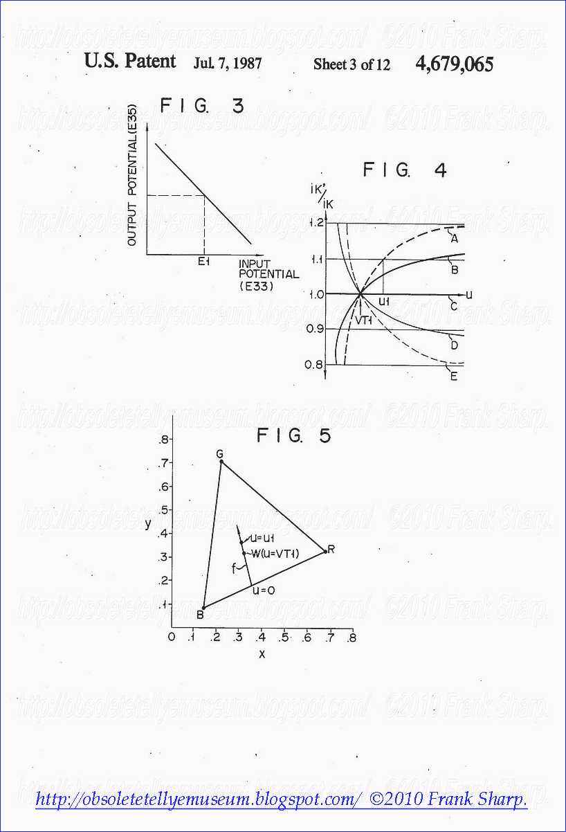
Comparator 35B has a characteristic as shown in FIG. 3. When the reference potential applied to the positive input (+) of comparator 35B is given to be E1 and the input and output potentials of comparator 35B are respectively plotted along the abscissa and ordinate, the output potential (E35B) decreases as the input potential (E33B) increases.
Level correction circuit 18B has such an electrical characteristic that the output DC level of signal E18B raises when DC control voltage E35B applied to control terminal 24 increases, while the output DC level of E18B falls when E35B decreases.
When the emission of cathode 21B is deteriorated (or a certain drift in the operating point of associated circuitries occurs), the corresponding cathode current I21B flowing into resistor 29 of circuit 20B becomes small. The potential of signal E33B from sampling circuit 33B is proportional to the magnitude of cathode current I21B which is obtained at the period of reference insertion pulse E17A (FIG. 2D). Since the sampling is performed only during the period T1 of reference insertion pulse E17A, the potential of signal E33B is independent of the period of picture signal L. Thus, when the deterioration of cathode emission occurs, the sampled output E33B is decreased regardless of the presence of any picture signal L.
Comparator 35B compares reference potential E1 with the potential of sampled output E33B. When a deterioration of the cathode emission occurs, comparator 35B generates DC control voltage E35B which is increased in accordance with the characteristic of FIG. 3. Then, the DC level of signal E18B from level correction circuit 18B is increased, thereby increasing the corresponding cathode current I21B.
On the contrary, when the cathode current increases, operation opposite to the operation described above is performed so as to decrease the corresponding cathode current. The increase/decrease operation point of the negative feedback control is stably converged to a point at which the difference between the reference potential E1 and the sampled output E33B becomes zero.
The cathode emission correction operation for R and G components may be performed in the same manner as that for the B component as described above. When the negative feedback control circuit is arranged to set the difference between the reference potential (E1) and the sampled output (E33) to be zero while the initial reference white is properly adjusted, the CRT biases for R, G, and B are automatically adjusted even if a deterioration in the cathode emission of CRT or a drift in the operating point of associated circuitries occurs. As a result, an automatic correction is so performed that the reference white is always maintained at a predetermined value.
The above operation will be exemplified using the circuit arrangement of the blue axis.
Assume here that the first grid (control grid) of each electron gun of CRT 21 is circuit-grounded, the voltage potential at cathode 21B and the current (I21B) flowing therethrough are respectively represented by uk and ik, and the cutoff voltage of cathode 21B is given to be Vcut. Under this assumption, cathode current ik is given as follows: ik=(K/Vcut3/2)(Vcut-uk)r ( 1)
where K is a proportional constant, and r is a specific constant of the CRT which is determined by the characteristic of the electron gun. Specific constant r generally falls within the range of 2.5 to 3.0.
When the input potential of comparator 35B (i.e, the potential of output E33B from sampling circuit 33B) is denoted by ui and the resistance of resistor 29 is denoted by R, input potential ui with respect to the circuit-ground is given to be: ui=R.ik (2)
Further, when the potential of output E35B from comparator 35B is assumed to be uA, the sensitivity of comparator 35B is assumed to be A and the potential of reference potential source 36 is assumed to be E1, the output potential uA is given as: uA=A(E1-ui) (3)
Accordingly, it can be seen than comparator 35B is a difference amplifier with a gain of A. When the potential of the signal component of reference insertion pulse E17A supplied to level correction circuit 18B is assumed to be VT1, the DC control sensitivity of circuit 18B is assumed to be B and the potential of output E18B from circuit 18B is assumed to be uB, the output potential uB is given as: uB=VT1+B.uA (4)
Furthermore, when the collector potential of transistor 25 is assumed to be uc, the resistance of resistor 27 is assumed to be R1, a resistance of resistor 26 is assumed to be R2 and the potential of voltage source Vcc is given to be Vcc, the collector potential uc is given as follows: uc=Vcc-(R2/R1)(uB-VBE1) (5)
where VBE1 denotes the base-emitter voltage of transistor 25. Potential uc is applied to cathode 21B via the base-emitter path of transistor 28.
A cathode potential uk at cathode 21B of CRT 21 is given as: uk=uc+VBE2 (6)
where VBE2 is the base-emitter voltage of transistor 28.
When equations (2) to (5) are substituted into equation (6), the following equation is obtained: ##EQU1## Equation (7) is substituted into equation (1), so that ##EQU2## In equation (9), Vcut, Vcc, VBE1, VBE2 and R2/R1 are all constants. Accordingly, a circuit design for the configuration of FIG. 1 enables the value of ΔV in equation (9) to be zero, that is, ΔV=0 (9')
Then, equation (10) can be rewritten as: ik=(K/Vcut3/2)[(R2/R1){VT1+A.B(E1-R.ik)}]r ( 11)
The cathode current ik, which nullifies the difference between input potential ui and reference potential E1 at comparator 35B, is given to be: ik=E1/R
The above equation is substituted into the right term of equation (11), so that ik=(K/Vcut3/2){(R2/R1)VT1}r ( 12)
Therefore, ik=E1R=(K/Vcut3/2){(R2/R1)VT1}r
The above equation may be rewritten as follows: E1=R.(K/Vcut3/2){(R2/R1)VT1}r ( 13)
When circuit constants VT1, Vcc, E1 and so on are selected so that equation (9') and E1 satisfy the relation of equation (13), the equation (8) holds. A current (ik)T1 flowing during the sampling period T1 (FIG. 2D) is stabilized at the following value: (ik)T1=E1/R=(Ik)T1 (14)
where Ik denotes the stabilized value of cathode current ik.
Meanwhile, cutoff voltage Vcut of the electron gun of CRT 21 depends on the spatial distance between the first and second grids. Variations in the spatial distance during the fabrication of CRTs bring unfavorable variations in cutoff voltage Vcut. When equation (13) is satisfied and a variation in Vcut is given to be ΔVcut, ΔV of equation (9) is given as: ΔV=Vcut+ΔVcut-{Vcc+VBE2+(R2/R1)VBE1} (15)
Upon the assumption of equation (9'), Vcut-{Vcc+VBE2+(R2/R1)VBE1}=0
so that equation (15) is rewritten as ΔV=ΔVcut. Current (ik)T1 flowing during the sampling period T1 is derived from equation (10) and it satisfies the following equation: ##EQU3## In this case, if a current error (which indicates a deviation from the target value of the cathode current) is given to be (Δik)T1, a relation (ik)T1=(Ik)T1+(Δik)T1 is obtained. According to equation (16), the right term of the above relation is given as: ##EQU4## A relation E1-R.(ik)T1=0 is obtained from equation (14), so that ##EQU5## if Vcut>>ΔVcut is satisfied and equation (17) is given to be ΔVcut=(R2/R1){A.B.R(Δik)T1}
then (ik)T1+(Δik)T1=(K/Vcut3/2){(R2/R1)VT1}r
Therefore, when the feedback control loop is arranged to satisfy the following inequality: (R2/R1)A.B.R>>ΔVcut/(Δik)T1 (18)
the current flowing during the sampling period T1 is kept substantially constant.
The circuit arrangement of FIG. 1 described above has the following disadvantage.
Assume that the voltage of a video signal is given to be u, that the cathode current with cutoff voltage Vcut is given to be ik, that the cathode current with cutoff voltage (Vcut+ΔVcut) is given to be ik', and that the voltage of a video signal with cutoff voltage (Vcut+ΔVcut) is given to be u+ΔVT1, then cathode currents ik and ik' are given as follows: ##EQU6## Therefore, the ratio of ik' to ik is given as: ##EQU7## It is apparent that the reference white of a CRT can be fixed at a prescribed constant value when the right term of equation (21) is constant. However, it is very hard to keep the value of the right term of equation (21) constant. This is because the right term of equation (21) cannot be made constant unless a condition that ΔVcut=0 (and ΔVT1=0) is satisfied. Only under this condition, does ik'/ik become constant. As previously described, cutoff voltage Vcut varies during the fabrication process of CRTs. It is almost impossible in practice to establish ΔVcut=0. Thus, a color television receiver is subjected to the variation ΔVcut, and the reference white cannot be kept constant throughout all levels (black level to white level) of the video signal.
The above problem of the prior art will be described with reference to the graphs shown in FIGS. 4 and 5. Referring to FIG. 4, voltage u of the video signal is plotted along the abscissa, and the change in ratio ik'/ik in accordance with variation ΔVcut is plotted along the ordinate. Each of curves A and B represents a change in ratio ik'/ik when variation ΔVcut occurs in the negative side with respect to Vcut (here the change of curve A in the negative side is greater than that of curve B). Each of curves D and E represents a change in ratio ik'/ik when variation Vcut occurs in the positive side with respect to Vcut (here the change of curve E in the positive side is greater than that of curve D). Curve C represents a desired ratio of ik'/ik obtained when ΔVcut=0.

As is apparent from FIG. 4, ik'/ik=1 is obtained (i.e., ratio ik'/ik becomes constant) only when ΔVcut=0. Ratio ik'/ik deviates from the center value of 1.0 according to the changes in variation ΔVcut. For instance, when the video signal voltage is set at ul in FIG. 4, ratio ik'/ik =1.1 is obtained. When the video signal voltage is set at VT1 (i.e., when the video signal voltage is represented by the voltage of reference insertion pulse E17A during the sampling period T1), ik'/ik=1 (constant) is obtained regardless of the change in ΔVcut. In other words, when the voltage of the video signal is identical with VT1, the reference white is fixed at a constant value. Otherwise, the reference white deviates from a target value, except for ik'/ik=1.0.
The deviation of the reference white will be discussed with reference to the chromaticity diagram of FIG. 5. Line f in FIG. 5 indicats a deviation in reference white of curve A in FIG. 4. Assume that R, G and B cathode currents are given by equations (19) and (20) and are respectively represented by iR, iG and iB which have a specific ratio (iR:iG:iB=1:1:1) so as to obtain the reference white W. The reference white is obtained only when the relation u=VT1 in FIG. 4 is established. For instance, when u=u1 as shown in FIG. 4 is considered, the current ratio is given to be: iR:iG:iB=1:1:1.1
Then, the current ratio changes. The deviation in the reference white due to this change is represented by line f in FIG. 5.
In the course of the circuit design of a color television receiver, it is almost impossible to ensure that the reference white comes to be constant for all actual CRTs, unless the values of respective elements such as voltages and resistances in the associated circuit arrangement are carefully determined in consideration of variations in the respective CRTs. Thus, the reference white is deviated in actual commercial products due to changes in the video signal level.
SUMMARY OF THE INVENTION
It is accordingly the object of the present invention to provide a color television receiver which can rep
roduce a picture with normal colors even if variations in the characteristic of a color CRT are caused by variations in the fabrication process of CRTs.To achieve the above object, a color television receiver of the invention is provided with special negative feedback loops for automatically adjusting the amplitude of each cathode driving voltage of R, G and B electron guns, so that the magnitude of each cathode current of R, G and B electron guns is converged to a given value.
According to the present invention, important and time-consuming reference white adjustment in the fabrication process of color television receivers can be simplified and stabilized by the operation of the special negative feedback loops. Further, according to the negative feedback operation, the adjusted reference white becomes insensitive to changes in the cathode emission of CRT due to aging etc. From this, even after the distribution of color television receivers to users, disadvantages (e.g., degradation of color reproduction fidelity) due to deviations in reference white can be automatically removed. Therefore, users can enjoy a good picture with normal color for a long time, without periodical reference white adjustment.
BRIEF DESCRIPTION OF THE DRAWINGS
FIG. 1 shows a prior art color television receiver having an automatic white control circuit;
FIGS. 2A to 2E are timing charts showing signals generated from the circuit components of FIG. 1;
FIG. 3 shows an operation characteristic of each comparator used in the circuit of FIG. 1;
FIG. 4 shows a graph explaining the problem of prior art, wherein the voltage u of a video signal is plotted along the abscissa and the change in ratio ik'/ik in accordance with the cutoff voltage variation ΔVcut is plotted along the ordinate;
FIG. 5 shows a chromaticity diagram explaining the problem of the prior art, wherein the line f indicates a deviation in reference white of curve A in FIG. 4;
FIG. 6 shows a color television receiver according to an embodiment of the present invention;
FIGS. 7A to 7G are timing charts explaining a typical operation of the embodiment shown in FIG. 6;
FIG. 8 shows an operation characteristic of each of comparators 53R, 53G and 53B used in the embodiment of FIG. 6;
FIG. 9 shows an operation characteristic of each of AGC amplifiers 58R, 58G and 58B used in the embodiment of FIG. 6;
FIGS. 10A to 10G are timing charts explaining another operation of the embodiment in FIG. 6;
FIGS. 11A to 11G are timing charts explaining still another operation of the embodiment in FIG. 6;
FIG. 12 shows a modification of the embodiment of FIG. 6;
FIG. 13 shows a circuit diagram of signal generator 171 used in FIG. 6;
FIG. 14 shows a circuit diagram of sampling circuit 33b used in FIG. 6;
FIG. 15 shows another circuit diagram of signal generator 171 used in FIG. 6;
FIG. 16 shows a waveform of signal E13 obtained when the circuit of FIG. 15 is employed; and
FIG. 17 shows a color television receiver according to another embodiment of the present invention, which corresponds to the combination of the disclosures of Japanese Patent Application Nos. 58-124607 and No. 58-124608 (both filed on July 11, 1983).
DETAILED DESCRIPTION OF THE PREFERRED EMBODIMENTS

A color television receiver according to the present invention will be described with reference to FIGS. 6 to 17. FIG. 6 is a block diagram of the color television receiver according to the present invention. The same reference numerals used in FIG. 6 denote the same parts as in FIG. 1, and a detailed description thereof will be omitted for the sake of simplicity.
The following description will be given chiefly to the key portion of the present invention. The function of a signal generator 171 is different from that of signal generator 17 in FIG. 1. The function of signal generator 171 will be described with reference to FIGS. 7A to 7G. Signals shown in FIGS. 7A to 7C are the same as those in FIGS. 2A to 2C, respectively. Signal generator 171 is arranged to generate not only a first reference insertion pulse P1 during a period T1 but also a second reference insertion pulse P2 during a period T2, as shown in FIG. 7D. Second reference insertion pulse P2 is generated within period T2 which is, e.g., delayed by 1 H from period T1 in the horizontal blanking (HB) period. The amplitude of second reference insertion pulse P2 is different from (larger than in this case) the amplitude of first reference insertion pulse P1. When the amplitude of pulse P1 corresponds to the condition that u=VT1 in FIG. 4, the amplitude of pulse P2 corresponds to the condition that, e.g., u=u1.
According to the present invention, the fact that the amplitude of P1 is different from the amplitude of P2 is important. That is, when pulse P1 is used to determine the condition u=VT1, pulse P2 is used to converge the value ik'/ik=1.1 on curve A in FIG. 4 to the value ik'/ik=1.0 on curve C. A reference insertion pulse E171A containing first and second reference insertion pulses P1 and P2 are supplied from an output terminal 171A of generator 171A to mixer 13. A gate pulse E171B containing first and second gate pulses GP1 and GP2 (FIGS. 7E and 7F) is obtained from an output terminal 171B of generator 171. The generation timing of gate pulses GP1 and GP2 is identical to or synchronized with the generation timing of insertion pulses P1 and P2.
Sampling circuits 33r, 33g and 33b respectively correspond to two sets of sampling circuits 33R, 33G and 33B in FIG. 1. Each of circuits 33r, 33g and 33b samples and holds the potential of corresponding signals E20R, E20G and E20B according to gate pulse E171B from signal generator 171. The sampled potentials of signals E20R, E20G and E20B respectively correspond to the magnitudes of cathode currents I21R, I21G and I21B during the durations of first and second insertion pulses P1 and P2. Capacitors Cr1, Cg1 and Cb1 hold the sampled potentials during the period T1 of pulse P1. Capacitors Cr2, Cg2 and Cb2 hold the sampled potentials during the period T2 of pulse P2.Sampled outputs E33r, E33g and E33b obtained during the period of first reference insertion pulse P1 are supplied to the respective negative inputs (-) of comparators 35R, 35G and 35B. Each positive input (+) of comparators 35R, 35G and 35B receives a first reference potential E1 from a first potential source 36. Outputs E35R, E35G and E35B from comparators 35R, 35G and 35B are respectively supplied to the control terminals 22, 23 and 24 of level correction circuits 18R, 18G and 18B.
Elements 18 to 20, 33 and 35 in FIG. 6 form DC negative feedback control loops for controlling the cathode biases of R, G and B electron guns in CRT 21. These control loops serve to equivalently shift each cutoff voltage Vcut (DC) of the R, G and B electron guns to a specific value which is determined by the reference potential E1 and which corresponds to the point u=VT1 in FIG. 4.
Sampled outputs E330r, E330g and E330b obtained during the period of second reference insertion pulse P2 are supplied to the respective negative inputs (-) of comparators 53R, 53G and 53B. Each positive input (+) of comparators 53R, 53G and 53B receives a second reference potential E2 from a second potential source 54. Outputs E53R, E53G and E53B from comparators 53R, 53G and 53B are respectively supplied to control input terminals 59, 60 and 61 of AGC amplifiers 58R, 58G and 58B. AGC amplifiers 58R, 58G and 58B are arranged between matrix circuits 12R, 12G and 12B and level correction circuits 18R, 18G and 18B, respectively.
The input/output characteristic of each of comparators 53R, 53G and 53B is shown in FIG. 8. In FIG. 8, the reference potential applied to the respective positive inputs (+) of comparators 53R, 53G and 53B is given to be E2, the input potential (E330) applied to the respective negative inputs (-) of these comparators is plotted along the abscissa, and the output voltage (E53) of these comparators is plotted along the ordinate. Thus, the output voltage (E53) of these comparators decreases when the input voltage (E330) increases, while the output voltage (E53) increases when the input voltage (E330) decreases.

Each of AGC amplifiers 58R, 58G and 58B has an input/output characteristic as shown in FIG. 9. In FIG. 9, DC control voltages (E53) applied to control input terminals 59, 60 and 61 of AGC amplifiers 58R, 58G and 58B are plotted along the abscissa. The gain α of each of AGC amplifiers 58R, 58G and 58B is plotted along the ordinate. When signals E12R, E12G and E12B are respectively inputted to AGC amplifiers 58R, 58G and 58B, amplifiers 58R, 58G and 58B provide outputs E58R, E58G and E58B whose voltages (amplitudes) respectively correspond not only to the amplitudes of signals E12R, E12G and E12B but also to the potentials of DC control voltages E53R, E53G and E53B. The higher the potential of control voltage (E53) becomes, the higher the amplitude of output voltage (E58) becomes. When the control voltage (E53) decreases, the output voltage (E58) decreases.
Elements 58, 18 to 20, 33 and 53 in FIG. 6 form AC negative feedback control loops for controlling the cathode driving voltages of the R, G and B electron guns in CRT 21. These control loops serve to converge each of cathode currents I21R, I21G and I21B (whose magnitudes respectively correspond to the amplitudes (AC) of signals E12R, E12G and E12B) of the R, G and B electron guns to a specific value which is determined by the reference potential E2.
The operation of the circuit shown in FIG. 6 will be described with reference to FIGS. 7 to 9. FIG. 7A shows video signal E11Y appearing at output terminal 11Y of television signal processing circuit 11; FIG. 7B shows output E15 from vertical blanking pulse shaper 15; and FIG. 7C shows output E16 from horizontal blanking pulse shaper 16. These signals E11Y, E15 and E16 are similar to those in FIGS. 2A to 2C. FIG. 7D shows reference insertion pulse E171A containing first and second reference insertion pulses P1 and P2 which appear at terminal 171A of signal generator 171. Pulses P1 and P2 are mixed in mixer 13 with video signal E11Y of FIG. 7A. Mixer 13 outputs a composite video signal E13 as shown in FIG. 7G. In FIG. 7G, the bottom potentials of signal components EP1 and EP2 respectively correspond to the top potentials of reference insertion pulses P1 and P2. FIGS. 7D and 7E respectively show gate pulses GP1 and GP2 obtained from terminal 171B of signal generator 171.
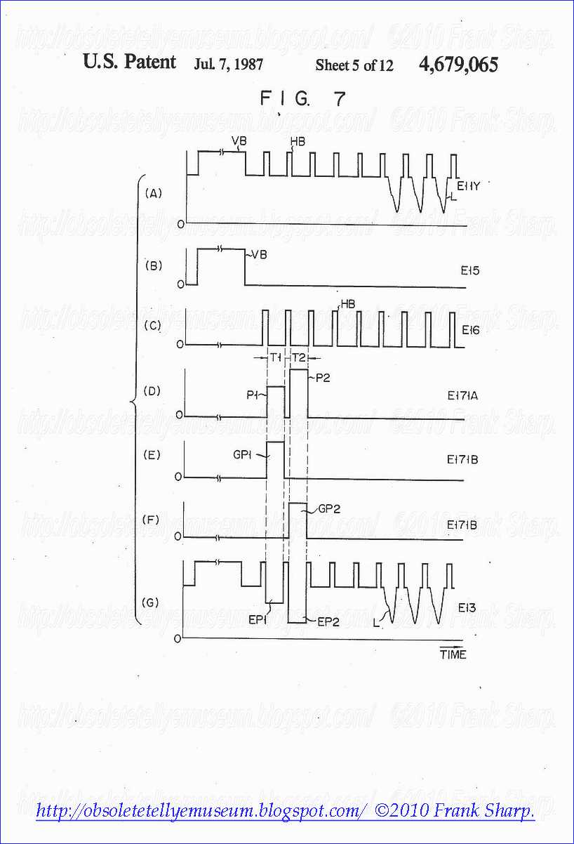
The potentials of signals E20R, E20G and E20B corresponding to the cathode currents I21R, I21G and I21B of CRT 21 during period T1 are sampled and held in sampling circuits 33r, 33g and 33b. Sampled outputs E33r, E33g and E33b are respectively supplied to comparators 35R, 35G and 35B and are compared with first reference potential E1. Level correction circuits 18R, 18G and 18B are controlled in accordance with the potentials of comparison outputs E35R, E35G and E35B from comparators 35R, 35G and 35B. The DC negative feedback operation of elements 18, 19, 20, 33 and 35 in FIG. 6 is the same as that in FIG. 1. However, according to the embodiment of the present invention, sampling circuits 33r, 33g and 33b are further operated during period T2 after period T1. After period T1, comparators 53R, 53G and 53B and AGC amplifiers 58R, 58G and 58B are actuated. The AC negative feedback operation of elements 58, 18 to 20, 33 and 53 will be explained below using the circuit elements of the blue axis.
As previously described, the amplitude of second reference insertion pulse P2 in period T2 is greater than that of first reference insertion pulse P1 in period T1. Namely, the amplitude of second reference insertion pulse P2 represents brighter white than the brightness of first reference insertion pulse P1. The potential of signal E20B which corresponds to cathode current I21B flowing during the period T2 is sampled in sampling circuit 33b, and the sampled output E330b is supplied to the negative input (-) of comparator 53B.
Reference potential E2 applied to the positive input (+) of comparator 53B is determined according to the following manner. Here, consideration will be given to a case wherein an error as indicated by the said equation (21) occurs, said equation (21) is: ##EQU8## The potential E2 of potential source 54 is preset such that the potential at the negative input (-) of comparator 53B, which is obtained when ik'/ik=1.0 is established (i.e., when cutoff voltage Vcut is stabilized), becomes equal to the potential at the positive input (+) of comparator 53B. From this, if ik'/ik=1.0, no potential difference appears between the inputs (+) and (-) of comparator 53B, and output E53B from comparator 53B becomes constant. Then, the gain of AGC amplifier 58B is converged to 1.0, and output E58B from amplifier 58B is also kept constant. In other words, the reference white is kept constant throughout all levels from the black level to the white level.

When variations in the fabrication process of CRT 21 cause variations in cutoff voltage Vcut of electron guns so as to generate the deviation ΔVcut (e.g., ik'/ik>1.0), cathode current I21B increases during period T2 so that sampled output E330b from sampling circuit 33b is increased. Then, sampled output E330b exceeds reference potential E2, and output E53B from comparator 53B is decreased in accordance with the characteristic as shown in FIG. 8. A decrease in output E53B from comparator 53B is equal to a decrease in control input of AGC amplifier 58B. Thus, the input-to-output gain of AGC amplifier 58B becomes small so that the drive voltage applied to cathode 21B of CRT 21 is decreased. Therefore, ik'/ik is controlled to approach the stabilized value of 1.0.
However, if ik'/ik<1.0, sampled output E330b from sampling circuit 33b is decreased, and output E53B from comparator 53B is increased. The gain of AGC amplifier 58B is increased to increase the drive voltage applied to cathode 21B of CRT 21. Even where ik'/ik.perspectiveto.1.0, comparator 53B and AGC amplifier 58B carry out the control operation to constantly maintain the relation ik'/ik=1.0.
The above operation will be described using mathematical expressions. When the cathode current flowing during the period T2 is given to be ik2, input potential ui2 applied to sampling circuit 33b is given as follows: ui2=R.ik2 (22)
When the sensitivity of comparator 53B and the reference potential are given to be a and E2, respectively, output potential uA2 from comparator 53B is given as follows: uA2=a(E2-ui2) (23)
When the control sensitivity of AGC amplifier 58B is given to be D, the input voltage applied to level correction circuit 18B is given to be VT2, the control sensitivity of level correction circuit 18B is given to be B, the output potential from comparator 35B is given to be uA, then an output potential uB2 from level correction circuit 18B is given as: uB2=VT2(1+D.uA2)+B.uA (24)
(24)
Cathode currents ikl and ik2 flowing during periods T1 and T2 can be obtained from equations (1) to (10) as: ##EQU9##
When circuit constants E2, VT2, etc. are selected such that reference potential E2 satisfies the following equation (27) in the same manner as in equation (13), equations (25) and (26) hold. E2=R(K/Vcut3/2){(R2/R1)VT2}r (27)
When equations (25) and (26) hold, currents (ik)T1 and (ik)T2 flowing during the sampling periods T1 and T2 are respectively stabilized at the following values: (ik)T1=E1/R=(IK)T1 (28) (ik)T2=E2/R=(IK)T2 (29)
When cutoff voltage Vcut varies due to deviations in the fabrication process of CRT 21, equation (20) can be rewritten in the embodiment as: ik'={K/(Vcut+ΔVcut)3/2 }[(R2/R1).α.(u+VT1)]r (30)
where α denotes the input-to-output gain of AGC amplifier 58B. Ratio ik'/ik is thus given as follows: ik'/ik={Vcut/(Vcut+ΔVcut}3/2 ×[α.{(u+ΔVT1)/u}]r (31)
As seen from the characteristic of FIG. 9, gain α of AGC amplifier 58B in equation (31) is controlled by the potential of output E53B from comparator 53B. Thus, a gain control is performed so as to obtain the relation ik'=ik.

In equation (31), ik'/ik=1.0 is obtained for u=VT1 and u=VT2. When VT1≠VT2 (e.g., VT2>VT1), the gain α can be calculated as follows: α={(Vcut+ΔVcut)/Vcut}3/2r (32)
In this case, VT1 becomes zero, and equation (31) is given as: ik'/ik=1.0 (33)
The reference white is thus constant throughout all levels (from black level to white level) of the video signal.
Unlike the current ratio of prior art given by equation (21), the current ratio of the present invention which is given by equation (33) is represented by line C in FIG. 4. Equation (33) is satisfied in all levels of the video signal, and hence the reference white is constant. This clearly demonstrates that no deviations from the reference white point W in FIG. 5 occur.
In the above description, the operation of the blue circuit is explained. The red and green circuits are operated in the same manner as in the blue circuit, thereby automatically controlling respective cathode driving voltages of R, G and B electron guns in CRT 21.
Although the above description is given to the case wherein the circuit of FIG. 6 operates according to the timing charts of FIGS. 7A to 7G, the circuit of FIG. 6 may be operated according to another way. For instance, as shown in FIGS. 10D to 10G, the second insertion pulse P2 is generated before the generation of first insertion pulse P1. Or, as shown in FIGS. 11D to 11G, the amplitude of second insertion pulse P2 may be smaller than that of first insertion pulse P1. Further, although not shown, the second insertion pulse P2 may be separated by two or more horizontal pulses HB from the first insertion pulse P1.
The locations of AGC amplifiers 58R, 58G and 58B are not limited to those shown in FIG. 6. So long as substantially the same effect as in the embodiment of FIG. 6 is obtained, the AGC amplifiers may be inserted in any positions in the video signal transmission line. For instance, as shown in FIG. 12, AGC amplifiers 58R, 58G and 58B may be respectively inserted between level correction circuits 18R, 18G and 18B and CRT drivers 19R, 19G and 19B.

FIG. 13 shows a circuit example of signal generator 171 used in FIG. 6. Horizontal blanking pulse HB of signal E16 is supplied via one input of an AND gate 130 to the clock input CK of a D flip-flop 131. The D input of flip-flop 131 receives its inverted Q output. The inverted Q output from flip-flop 131 is supplied to the clock input CK of a D flip-flop 132 whose D input receives its inverted Q output. Each reset input R of flip-flops 131 and 132 receives vertical blanking pulse VB of signal E15. The inverted Q output from flip-flop 131 is supplied via an inverter 133 to one input of a NAND gate 134. The other input of gate 134 receives the inverted Q output of filp-flop 132 via an inverter 135. The NANDed output from gate 134 is supplied to the other input of AND gate 130. The inverted Q output from flip-flop 131 and the output from inverter 135 are respectively inputted to an AND gate 136. The output from inverter 133 is used as the first gate pulse GP1 (FIGS. 7E, 10E or 11E). The ANDed output from gate 136 is used as the second gate pulse GP2 (FIGS. 7F, 10F or 11F). Pulses GP1 and GP2 obtained from elements 133 and 136 constitute the gate pulse E171B.
The logical level of gate pulse GP1 from inverter 133 controls the on/off of an analog switch 137. When the level of pulse GP1 is high (FIG. 7E), switch 137 is closed so that a first insertion potential source V1 provides the high-level portion of first reference insertion pulse P1 (during T1 in FIG. 7D). When the level of pulse GP1 is low, switch 137 is opened so that pulse P1 disappears.
The logical level of gate pulse GP2 from AND gate 136 controls the on/off of an analog switch 138. When the level of pulse GP2 is high (FIG. 7F), switch 138 is closed so that a second insertion potential source V2 provides the high-level portion of second reference insertion pulse P2 (during T2 in FIG. 7D). When the level of pulse GP2 is low, switch 138 is opened so that pulse P2 disappears. Pulses P1 and P2 obtained from elements 137 and 138 constitute the reference insertion pulse E171A.
FIG. 14 shows a circuit example of sampling circuit 33b used in FIG. 6. The circuit configuration of 33r and 33g may be the same as that shown in FIG. 14. Signal E20B representing cathode current I21B of the B electron gun in CRT 21 is supplied via a buffer 140 to analog switches 141 and 142. The on/off of switch 141 is controlled according to the logical level of first gate pulse GP1. The on/off of switch 142 is controlled according to the logical level of second gate pulse GP2.
When switch 141 is closed by the high-level of pulse GP1, the potential of signal E20B, which indicates the magnitude of cathode current I21B at period T1 (FIG. 7D), is applied to capacitor Cb1. Then, capacitor Cb1 is charged by a voltage corresponding to the potential of signal E20B. The charged voltage (sampled potential) at capacitor Cb1 is supplied to comparator 35B. When the level of pulse GP1 is low, switch 141 is opened so that the charged voltage is held at capacitor Cb1.
When switch 142 is closed by the high-level of pulse GP2, the potential of signal E20B, which indicates the magnitude of cathode current I21B at period T2 (FIG. 7D), is applied to capacitor Cb2. Then, capacitor Cb2 is charged by a voltage corresponding to the potential of signal E20B. The charged voltage (sampled potential) at capacitor Cb2 is supplied to comparator 53B. When the level of pulse GP2 is low, switch 142 is opened so that the charged voltage is held at capacitor Cb2.

FIG. 15 shows another circuit example of signal generator 171 used in FIG. 6. Horizontal blanking pulse HB of signal E16 is supplied via one input of an AND gate 150 to the clock input CK of a D flip-flop 151. The D input of flip-flop 151 receives its inverted Q output. The inverted Q output from flip-flop 151 is supplied to the clock input CK of a D flip-flop 152 whose D input receives its inverted Q output. Each reset input R of flip-flops 151 and 152 receives vertical blanking pulse VB of signal E15. The inverted Q output from flip-flop 152 is supplied to the other input of AND gate 150. Signal E15 is supplied to the clock input CK of a D flip-flop 153 whose D input receives its inverted Q output. The inverted Q output from flip-flop 153 is supplied via an inverter 154 to one input of an AND gate 155. The other input of gate 155 receives the Q output from flip-flop 151. The ANDed output from gate 155 is used as the first gate pulse GP1. The inverted Q output from flip-flop 153 and the Q output from flip-flop 151 are inputted to an AND gate 156. The ANDed output from gate 156 is used as the second gate pulse GP2. Pulses GP1 and GP2 obtained from elements 155 and 156 constitute the gate pulse E171B.
The logical level of gate pulse GP1 from AND gate 155 controls the on/off of an analog switch 157. When the level of pulse GP1 is high, switch 157 is closed so that first insertion potential source V1 provides the high-level portion of first reference insertion pulse P1. When the level of pulse GP1 is low, switch 157 is opened so that pulse P1 disappears.
The logical level of gate pulse GP2 from AND gate 156 controls the on/off of an analog switch 158. When the level of pulse GP2 is high, switch 158 is closed so that second insertion potential source V2 provides the high-level portion of second reference insertion pulse P2. When the level of pulse GP2 is low, switch 158 is opened so that pulse P2 disappears. Pulses P1 and P2 obtained from elements 157 and 158 constitute the reference insertion pulse E171A.
FIG. 16 shows a waveform of signal E13 obtained when the circuit of FIG. 15 is used with the configuration of FIG. 6. According to the circuit of FIG. 13, signal components EP1 and EP2 in video signal E13, which respectively correspond to first and second insertion pulses P1 and P2, appear in one vertical scanning period. On the contrary, according to the circuit of FIG. 15, only signal component EP1 corresponding to pulse P1 appears in a present vertical scanning period, and only signal component EP2 corresponding to pulse P2 appears in the next vertical scanning period. In other words, according to the circuit of FIG. 15, the DC negative feedback loop of elements 18 to 20, 33 and 35 (FIG. 6) is activated based on the component EP1 in one vertical scanning period, while the AC negative feedback loop of elements 58, 18 to 20, 33 and 53 (FIG. 6) is activated based on the component EP2 in the next vertical scanning period.

FIG. 17 shows another embodiment of the present invention. According to the embodiment of FIG. 17, application of excessive driving voltages to the respective cathodes of CRT 21 immediately after the power-on of the color television receiver can be prevented by the special circuit elements (51X to 57X). Since the CRT is protected from intermittent excessive driving at each time of power-on, the service life of the CRT is extended. In addition, a stable picture is reproduced on the CRT after the power-on of television receiver, thereby avoiding discomfort to the viewers. The special circuit elements 51X to 57X are disclosed in U.S. patent application No. 628,984 which was filed by the same applicant as the present application. All disclosures of this Japanese Patent Application No. 58-124607 are incorporated in the present application.


TOSHIBA TA8751AN
TOSHIBA BIPOLAR LINEAR INTEGRATED CIRCUIT SILICON MONOLITHIC
TA8751AN
AUTOMATIC KINE BIAS (AKB)
RGB INTERFACE+
TA8751AN possesses functions that optimize the CRT
drive conditions in televisions, and is an IC that
automates the previously complex cutoff adjustment and
drive adjustment non-adjustment. .
It has an RGB TEXT input pin, so TV signal and TEXT ignal can be switched between rapidly.
AKB (AUTOMATIC KINE BIAS) Circuits take the previously complex adjustment of CRT drive
circuits and automates by absorbing the 3-color dispersion of the CRT. It is therefore
necessary to design the CRT drive circuit in an AKB centered state to allow efficient
absorption of the CRT's dispersion.
The primary color input on the TV side takes the form of DC coupling, so please set input
levels so that the contrast control and brightness control in previous stages are under the
following conditions in the center.
The TV's primary colors are DC coupled, so brightness
control from previous stages can be utilized.
hen the power is off and the CRT is
not warmed up, as a beam current
does not flow to cutoff and drive
detection interval, voltage is not
obtainable from the sense pin.
Accordingly, for operation so that
current flows to the CRT for both cut
adjustment and drive adjustment, the
CRT starts from a white screen the
instant it warms up.
In order to prevent this, the soft start
circuit returns the output DC voltage
and operates so that if pin 17 exceeds
a fixed value, cutoff adjustment is
fixed on the black side.
Vertical blanking input
Input pin for the vertical blanking
pulse that determines the timing of
the reference pulse for the cutoff
adjustment and drive adjustment.
The first 2H interval after the leading
edge of the vertical blanking is the
cutoff reference level, while the next
2H interval is the drive reference
level.
H timing is created by the horizontal
blanking of pin 14.
B sense
G sense
R sense
Detection pin for the CRT beam
current.
The current that flows to the CRT
cathode as a result of the reference
pulse inserted for cutoff adjustment
and drive adjustment is converted to a
voltage and detected by detection
resistance. White balance can be
changed by varying detection
resistance.
The internal comparator operates in
tune with the timing of the reference
pulse.
TDA8178S TV VERTICALDEFLECTION BOOSTER:DESCRIPTION
Designedfor monitors and high performanceTVs,
the TDA8178Svertical deflection booster delivers
flyback voltages up to 90V.
The TDA8178S operates with supplies up to 42V
and provides up to 2App output current to drive to
yoke.
The TDA8178Sis offeredinHEPTAWATTpackage.
.FLYBACK GENERATOR
.THERMAL PROTECTION
.REFERENCE VOLTAGE.
TDA4950 TV EAST/WEST CORRECTION CIRCUIT:
DESCRIPTION
The T
DA4950 is a monolithic integrated circuit in a8 pin minidip plastic package designed for use in
the east-west pin-cushion correction by driving a
diode modulator in TV and monitor applications.
.SQUARE GENERATOR FOR PARABOLIC
CURRENT
.EXTERNAL KEYSTONE ADJUSTMENT (sym-
metry of the parabola)
.INPUT FOR DYNAMIC FIELD CORRECTION
(beam current change)
.STATIC PICTURE WIDTH ADJUSTMENT
.PULSE-WIDTH MODULATOR
.FINAL STAGE D-CLASS WITH ENERGY RE-
DELIVERY
.PARASITIC
PARABOLA
SUPPRESSION,
DURING FLYBACK TIME OF THE VERTICAL
SAWTOOTH.
TEA5101A - RGB HIGH VO
LTAGE AMPLIFIER BASIC OPERATION AND APPLICATIONS:The control of state-of-the-art color cathode ray
tubes requires high performance video amplifiers
which must satisfy both tube and video processor
characteristics.
When considering tube characteristics (see Fig-
ures 13 and 14),we note that a 130V cutoff voltage
is necessary to ensure a 5mA peak current.How-
ever 150V is a more appropriate value if the satu-
ration effect of the amplifier is to be taken into
account. As the dispersion range of the three guns
is ± 12%, the cutoff voltage should be adjustable
from 130V to 170V. The G2 voltage, from 700 to
1500V allows overall adjustment of the cutoff volt-
age for similar tube types.
A 200V supply voltage of the video amplifier is
necessary to achieve a correct blanking operation.
In addition, the video amplifier should have an
output saturation voltage drop lower than 15V, as
a drive voltage of 130V (resp. 115V) is necessary
to obtain a beam current of 4 mA for a gun which
has a cutoff point of 170V (resp. 130V).
Note : For all the calculations discussed above, the
G1 voltage is assumed to be 0V.
The video processor characteristics must also be
considered. As it generally delivers an output volt-
age of 2 to 3V, the video amplifier must provide a
closed loop DC g
ain of approximately 40.The video amplifier dynamic performances must
also meet the requirements of good definition even
with RGB input signals (teletext,home computer...),
e.g. 1mm resolution on a 54cm CRT width scanned
in 52µs. Consequently, a slew rate better than
2000V/µs, i.e. rise and fall times lower than 50ns,
is needed. In addition, transition times must be the
same for the three channels so as to avoid coloured
transitions when displaying white characters. The
bandwidth of a video amplifier satisfying all these
requirements must be at least 7MHz for high level
signals and 10MHz for small signals.
One major feature of a video amplifier is its capa-
bility to monitor the beam current of the tube. This
function is necessary with modern video proces-
sors:
- for automatic adjustment of cutoff and also, where
required,video gain in order to improve the long
term performances by compensation for aging
effects through the life of the CRT. This adjust-
ment can be done either sequentially (gun after
gun) or in a parallel mode.
- for limiting the average beam current
A video amplifier must also be flashover protected
and provide high crosstalk performances. Cros-
stalk effects are mainly caused by parasitic capaci-
tors and thus increase with the signal frequency. A
crosstalk level of -20dB at 5MHz is generally ac-
ceptable.
Table 1 summarizes the main features of a high
performance video amplifier.
Table 1 :
Main Features of a High Performance
Video Amplifier
Maximum Supply Voltage
220V
Output voltage swing "Average"
100V
Output voltage swing "Peak"
130V
Low level saturation (refered to VG1)
15V
Closed loop gain
40
Transition time
50ns
Large signal bandwidth
7MHz
Small signal bandwidth
10MHz
Beam current monitoring
Flash over protection
Crosstalk at 5MHz
-20dB
The SGS-THOMSON Microelectronics TEA5101A
is a high performance and large bandwidth 3 chan-
nel video amplifier which fulfills all the criteria dis-
cussed above. Designed in a 250V DMOS bipolar
technology, it operates with a 200V power supply
and can deliver 100V peak-to-peak output signals
with rise and fall times equal to 50ns.
The 5101A features a large signal bandwidth of
8MHz, which can be extended to 10MHz for small
signals (50 Vpp).
Each channel incorporates a PMOS transistor to
monitor the beam current. The circuit provides
internal protection against electrostatic discharges
and high voltage CRT discharges.
The best utilization of the TEA 5101A high perform-
ance features such as dynamic characteristics,
crosstalk,or flashover protection requires opti-
mized application implementation. This aspect will
be discussed in the fourth part of this document.
I.1 - Input Stage
The differential input stage consists of the transistor
T1 and T2 and the resistors R4,R5 and R6.
This stage is biased by a voltage source T3,R1,R2
and R3.
VB(T1) = (1 + R2
R3) x VB(T3) ≅ 3.8V
Each amplifier is biased by a separate voltage
source in order to reduce internal crosstalk. The
load of the input stage is composed of the transistor
T4 (cascode configuration) and the resistor R7. The
cascode configuration has been chosen so as to
reduce the Miller input capacitance. The voltage
gain of the input stage is fixed by R7 and the emitter
degenerati
on resistors R5,R6,and the T1,T2 internalemitter resistances. The voltage gain is approxi-
mately 50dB.
Using a bipolar transistor T4 and a polysilicon re-
sistor R7 gives rise to a very low parasitic capaci-
tance at the output of this stage (about 1.5pF).
Hence the rise and fall times are about 50ns for a
100V peak-to-peak signal (between 50V and
150V).
I.2 - Output Stage
The output stage is a quasi-complementary class
B push-pull stage. This design ensures a symetrical
load of the first stage for both rising and falling
signals. The positive output stage is made of the
DMOS transistor T5,and the negative output stage
is made of the transistors PMOS T6 and DMOS T7.
The compound configuration T6-T7 is equivalent to
a single PMOS. A single PMOS transistor capable
of sinking the total current would have been too
large.
By virtue of the symetrical drive properties of the
output stage the rise and fall times are equal (50ns
for 100V DC output voltage).
I.3 - Beam Current Monitoring
This function is performed by the PMOS transistor
T8 in source follower configuration. The voltage on
the source (cathode output) follows the gate volt-
age (feedback output). The beam current is ab-
sorbed via T8 . On the drain of T8, this current will
be monitored by the videoprocessor.
I.4 - Protection Circuits
I.4.1 - MOS protection
Four zener diodes DZ(1-4) are connected between
gate and source of each MOS in order to prevent
the voltage from reaching the breakdown volt-
age.Hence the VGS voltage is internally limited to
± 15V.
I.4.2 - Protection against electrostatic dis-
charges
All the input/output pins of the TEA5101A are pro-
tected by the diodes D1-D7 which limit the overvol-
tage due to ESD.
I.4.3 - Flashover Protection
A high voltage and high current diode D5 is con-
nected between each output and the high voltage
power supply. During a flash, most of the current is
generally absorbed by the spark gap connected to
the CRT socket. The remaining current is absorbed
by the high voltage decoupling capacitor through
the diode D5. Hence the cathode voltage is
clamped to the supply voltage and the output volt-
age does not exceed this value.
I.1 - Voltage Amplifier
II.1.1 - Bias conditions Vin = Vref
The bias point is fixed by the feedback resistor
Rf,the bias resistor Rp, and by the internal refer-
ence voltage when Vin = Vref.
If VO is the output voltage (pin 9) :
VO = (1 + Rf
Rp) x Vref (1)
In this state T1 and T2 are conducting. A current
flows in R7 and T4 soT5 is on. The T5 drain current
is fed to the amplifier input through the feedback
resistor. The current in R7 is:
I(R7) = VDD − VO − VGS(T5)
R7
≅ VDD − VO
R7
and the current in T5 and Rf is :
I(T5) = VO − Vref
Rf
≅ VO
Rf
Thus the total current absorbed by each channel of
the TEA5101A is :
VDD
R7 + VO x (1
Rf − 1
R7)
The cathode (pin 7) output voltage is:
VO + VGS(T8) = VO
The beam current is absorbed by T8 and Rm. The
voltage developed across Rm by this current is fed
to the videoprocessor in order to monitor the beam
current.
II.1.2 - Dynamic operation
The TEA5101A operates as a closed loop amplifier,
with its voltage gain fixed by the resistors Rf and
Re.
Since the open loop gain A is not infinite, the resistor
Rp and the input impedance Rin must be consid-
ered.Hence the voltage gain is
G = − Rf
Re x
1
1 + 1
A (1 +
Rf
Rp ⁄ ⁄ Re ⁄ ⁄ Rin)
(2)
II.1.2.1 - Input voltage Vin < Vref (black picture)
In this case the current flowing in R7 and T1 de-
creases whilst the collector voltage of T4 and the
output voltage both increase. In the extreme case,
I(T1) = I(R7) = 0 and VO= VDD-VGS(T5)
In order to charge the tube capacitor the voltage is
fed to the cathode output in two ways:
- through the PMOS (with a VGS difference) for the
low frequency part
- through the capacitor C for the high frequency
part (output signal leading e
dge)To correctly transmit the rising edge, the value of
the capacitor C must be high compared to CL.
With the current values used (C = 1nF,CL = 10pF),
the attenuation is very small (0.99)
II.1.2.2 - Input voltage Vin > Vref (white picture)
In this case,the current in R7 and T1 increases with
an accompanying drop of T4’s collector voltage until
T1 and T4 are saturated. At this point:
VO ≅ VC(T4) ≅ VCC
During a high to low transition (i.e. black-white
picture), the beam current is absorbed in two ways:
- through the capacitor C and the compound
PMOS T6-T7 for the high frequency part (falling
edge)
- through the PMOS T8 and the resistor Rm for the
low frequency part.
II.2 - Beam Current Monitoring
II.2.1 - Stationary state
The beam current monitoring is performed by the
PMOS T8 and the resistor Rm. When measuring low
currents (leakage, quasi cutoff),the Rm value is
generally high. When measuring high currents
(drive, average or peak beam current),Rm is gen-
erally bypassed by a lower impedance.
It should be noted that the current supplied by the
three guns flows through this resistor.Hence,with
too large a value for the resistor Rm,the cathode
voltage of the tubes will become too high for the
required operating current values.This is a funda-
mental difference between the TEA5101A and dis-
crete video amps. In discrete video amps, the
current monitoring transistor is a high voltage PNP
bipolar which may saturate. In this case the beam
current can flow through the transistor base and it
is no longer monitored by the video processor. This
effect does not occur with the TEA 5101A.
II.2.2 - Transient phase : low current measure-
ments
The cut-off adjustment sequence is generally as
follows:
In a first step, the cathode is set to a high voltage
(180V) in order to blank the CRT and to measure
the leakage current. In a second step, the tube is
slighly switched on to measure a very low current
(quasi cut-off current). This operation is performed
by setting the cathode voltage to about 150V and
adjusting it until the proper current is obtained. The
maximum time available to do this operation is
generally about 52µs.
Figure 3 shows the simplified diagram of the
TEA5101A output, the voltages during the different
steps,and the stationary state the system must
reach for correct adjustment.
I.1 - Voltage Amplifier
II.1.1 - Bias conditions Vin = Vref
The bias point is fixed by the feedback resistor
Rf,the bias resistor Rp, and by the internal refer-
ence voltage when Vin = Vref.
If VO is the output voltage (pin 9) :
VO = (1 + Rf
Rp) x Vref (1)
In this state T1 and T2 are conducting. A current
flows in R7 and T4 soT5 is on. The T5 drain current
is fed to the amplifier input through the feedback
resistor. The current in R7 is:
I(R7) = VDD − VO − VGS(T5)
R7
≅ VDD − VO
R7
and the current in T5 and Rf is :
I(T5) = VO − Vref
Rf
≅ VO
Rf
Thus the total current absorbed by each channel of
the TEA5101A is :
VDD
R7 + VO x (1
Rf − 1
R7)
The cathode (pin 7) output voltage is:
VO + VGS(T8) = VO
The beam current is absorbed by T8 and Rm. The
voltage developed across Rm by this current is fed
to the videoprocessor in order to monitor the beam
current.
II.1.2 - Dynamic operation
The TEA5101A operates as a closed loop amplifier,
with its voltage gain fixed by the resistors Rf and
Re.
Since the open loop gain A is not infinite, the resistor
Rp and the input impedance Rin must be consid-
ered.Hence the voltage gain is
G = − Rf
Re x
1
1 + 1
A (1 +
Rf
Rp ⁄ ⁄ Re ⁄ ⁄ Rin)
(2)
II.1.2.1 - Input voltage Vin < Vref (black picture)
In this case the current flowing in R7 and T1 de-
creases whilst the collector voltage of T4 and the
output voltage both increase. In the extreme case,
I(T1) = I(R7) = 0 and VO= VDD-VGS(T5)
In order to charge the tube capacitor the voltage is
fed to the cathode output in two ways:
- through the PMOS (with a VGS difference) for the
low frequency part
- through the capacitor C for the high frequency
part (output signal leading edge)
To correctly transmit the rising edge, the value of
the capacitor C must be high compared to CL.
With the current values used (C = 1nF,CL = 10pF),
the attenuation is very small (0.99)
II.1.2.2 - Input voltage Vin > Vref (white picture)
In this case,the current in R7 and T1 increases with
an accompanying drop of T4’s collector voltage until
T1 and T4 are saturated. At this point:
VO ≅ VC(T4) ≅ VCC
During a high to low transition (i.e. black-white
picture), the beam current is absorbed in two ways:
- through the capacitor C and the compound
PMOS T6-T7 for the high frequ
ency part (fallingedge)
- through the PMOS T8 and the resistor Rm for the
low frequency part.
II.2 - Beam Current Monitoring
II.2.1 - Stationary state
The beam current monitoring is performed by the
PMOS T8 and the resistor Rm. When measuring low
currents (leakage, quasi cutoff),the Rm value is
generally high. When measuring high currents
(drive, average or peak beam current),Rm is gen-
erally bypassed by a lower impedance.
It should be noted that the current supplied by the
three guns flows through this resistor.Hence,with
too large a value for the resistor Rm,the cathode
voltage of the tubes will become too high for the
required operating current values.This is a funda-
mental difference between the TEA5101A and dis-
crete video amps. In discrete video amps, the
current monitoring transistor is a high voltage PNP
bipolar which may saturate. In this case the beam
current can flow through the transistor base and it
is no longer monitored by the video processor. This
effect does not occur with the TEA 5101A.
II.2.2 - Transient phase : low current measure-
ments
The cut-off adjustment sequence is generally as
follows:
In a first step, the cathode is set to a high voltage
(180V) in order to blank the CRT and to measure
the leakage current. In a second step, the tube is
slighly switched on to measure a very low current
(quasi cut-off current). This operation is performed
by setting the cathode voltage to about 150V and
adjusting it until the proper current is obtained. The
maximum time available to do this operation is
generally about 52µs.
Figure 3 shows the simplified diagram of the
TEA5101A output, the voltages during the different
steps,and the stationary state the system must
reach for correct adjustment.
I.1 - Voltage AmplifierII.1.1 - Bias conditions Vin = Vref
The bias point is fixed by the feedback resistor
Rf,the bias resistor Rp, and by the internal refer-
ence voltage when Vin = Vref.
If VO is the output voltage (pin 9) :
VO = (1 + Rf
Rp) x Vref (1)
In this state T1 and T2 are conducting. A current
flows in R7 and T4 soT5 is on. The T5 drain current
is fed to the amplifier input through the feedback
resistor. The current in R7 is:
I(R7) = VDD − VO − VGS(T5)
R7
≅ VDD − VO
R7
and the current in T5 and Rf is :
I(T5) = VO − Vref
Rf
≅ VO
Rf
Thus the total current absorbed by each channel of
the TEA5101A is :
VDD
R7 + VO x (1
Rf − 1
R7)
The cathode (pin 7) output voltage is:
VO + VGS(T8) = VO
The beam current is absorbed by T8 and Rm. The
voltage developed across Rm by this current is fed
to the videoprocessor in order to monitor the beam
current.
II.1.2 - Dynamic operation
The TEA5101A operates as a closed loop amplifier,
with its voltage gain fixed by the resistors Rf and
Re.
Since the open loop gain A is not infinite, the resistor
Rp and the input impedance Rin must be consid-
ered.Hence the voltage gain is
G = − Rf
Re x
1
1 + 1
A (1 +
Rf
Rp ⁄ ⁄ Re ⁄ ⁄ Rin)
(2)
II.1.2.1 - Input voltage Vin < Vref (black picture)
In this case the current flowing in R7 and T1 de-
creases whilst the collector voltage of T4 and the
output voltage both increase. In the extreme case,
I(T1) = I(R7) = 0 and VO= VDD-VGS(T5)
In order to charge the tube capacitor the voltage is
fed to the cathode output in two ways:
- through the PMOS (with a VGS difference) for the
low frequency part
- through the capacitor C for the high frequency
part (output signal leading edge)
To correctly transmit the rising edge, the value of
the capacitor C must be high compared to CL.
With the current values used (C = 1nF,CL = 10pF),
the attenuation is very small (0.99)
II.1.2.2 - Input voltage Vin > Vref (white picture)
In this case,the current in R7 and T1 increases with
an accompanying drop of T4’s collector voltage until
T1 and T4 are saturated. At this point:
VO ≅ VC(T4) ≅ VCC
During a high to low transition (i.e. black-white
picture), the beam current is absorbed in two ways:
- through the capacitor C and the compound
PMOS T6-T7 for the high frequency part (falling
edge)
- through the PMOS T8 and the resistor Rm for the
low frequency part.
II.2 - Beam Current Monitoring
II.2.1 - Stationary state
The beam current monitoring is performed by the
PMOS T8 and the resistor Rm. When measuring low
currents (leakage, quasi cutoff),the Rm value is
generally high. When measuring high currents
(drive, average or peak beam current),Rm is gen-
erally bypassed by a lower impedance.
It should be noted that the current supplied by the
three guns flows through this resistor.Hence,with
too large a value for the resistor Rm,the cathode
voltage of the tubes will become too high for the
required operating current values.This is a funda-
mental difference between the TEA5101A and dis-
crete video amps. In discrete video amps, the
current monitoring transistor is a high voltage PNP
bipolar which may saturate. In this case the beam
current can flow through the transistor base and it
is no longer monitored by the video processor. This
effect does not occur with the TEA 5101A.
II.2.2 - Transient phase : low current measure-
ments
The cut-off adjustment sequence is generally as
follows:
In a first step, the cathode is set to a high voltage
(180V) in order to blank the CRT and to measure
the leakage current. In a second step, the tube is
slighly switched on to measure a very low current
(quasi cut-off current). This operation is performed
by setting the cathode voltage to about 150V and
adjusting it until the proper current is obtained. The
maximum time available to do this operation is
generally about 52µs.
Figure 3 shows the simplified diagram of the
TEA5101A output, the voltages during the different
steps,and the stationary state the system must
reach for correct adjustment.
During the blanking phase, the tube is switched off,
the PMOS is switched off and its VGS voltage is
equal to the pinch-off voltage (about 1.5V). The
voltages at the different nodes are shown in figure
3 (V(9) = 180V, V(k) = 181.5V). The falling edge of
the cutoff pulse is instantaneously transmitted by
the capacitor C. When the stationary state is
reached, the cathode voltage will be 152.5V if the
voltage on pin 9 is 150V, as the VGS voltage of the
conducting PMOS is about 2.5V.
We can see that the voltage
on C must increase by
an amount of ∆Vc = 1V. This charge is furnished by
the tube capacitor which is discharged by an
amount of ∆VCL = 29V with a time constant equal
to R x CL (10 ns). By considering the energy
balance, we can calculate the maximum charge
∆Vmax that CL can furnished to C
∆Vmax = √CL
C x ∆VCL ≅ 3V
Since this voltage is greater than ∆VC, the capacitor
C can be charged and the stationary state is
reached without any contribution being required
from the tube current,i.e. the whole tube current
can flow through the PMOS and the adjustment can
be performed correctly.
Considering higher voltage and beam current
swings, the margin is greater because:
- the voltage swing across the tube capacitor is
greater
- the tube current is higher and the picture is not
disturbed even if part of the beam current is used
to charge the capacitor C.
No comments:
Post a Comment
The most important thing to remember about the Comment Rules is this:
The determination of whether any comment is in compliance is at the sole discretion of this blog’s owner.
Comments on this blog may be blocked or deleted at any time.
Fair people are getting fair reply. Spam and useless crap and filthy comments / scrapers / observations goes all directly to My Private HELL without even appearing in public !!!
The fact that a comment is permitted in no way constitutes an endorsement of any view expressed, fact alleged, or link provided in that comment by the administrator of this site.
This means that there may be a delay between the submission and the eventual appearance of your comment.
Requiring blog comments to obey well-defined rules does not infringe on the free speech of commenters.
Resisting the tide of post-modernity may be difficult, but I will attempt it anyway.
Your choice.........Live or DIE.
That indeed is where your liberty lies.
Note: Only a member of this blog may post a comment.