


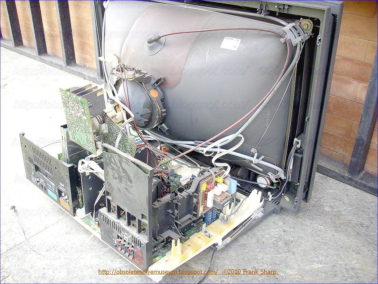


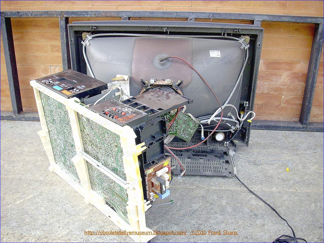


This is the PHILIPS 2nd generation 100HZ digital scanrate from PHILIPS.
The invention relates to an arrangement for converting an original picture signal representing a sequence of frames, each of which is composed of two interlaced fields, into a converted picture signal which has a double field frequency with respect to the original picture signal.
When converting a picture signal into such a converted picture signal which, with respect to the original picture signal, has a double field frequency, there is the problem that every second field of the converted picture signal must be newly generated, because no corresponding field of the original picture signal is available with respect to time and also with respect to the picture information.
In simple arrangements for doubling the field frequency, every field is doubled. A moving object in the fields of the converted picture signal is imaged twice in the same position before it jumps to the next position in the two subsequent fields. Since the human eye cannot follow these jumps, it is incident on the average speed of motion and observes a moving object from field to field at different positions. This leads to a double structure and motion blurr.
In other arrangements for field doubling of a picture signal a motion compensation is therefore provided by means of which the motion between two fields of the original picture signal is determined so that the motion can be taken into account in fields of the converted picture signal to be generated therebetween as a function of time and a corresponding interpolation can be performed. However, such arrangements have the further problem that possibly present noise is also to be reduced and that the line flicker, which still occurs in spite of the doubling of the field frequency in picture signals generated by way of interlaced scanning, is to be reduced. In the state of the art arrangements are only known in which a motion compensation is combined either with a noise reduction or with a line flicker reduction.
- Right side all Power part and large signal panel
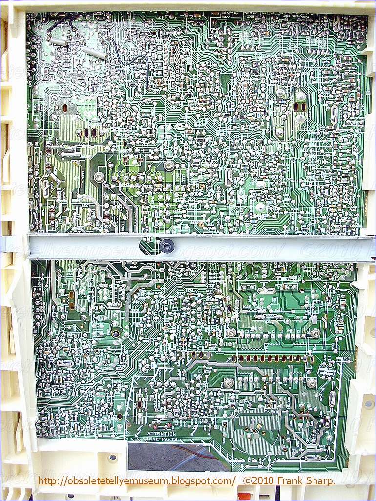
- Left side all signal processing and small signal panel
Description of circuits:
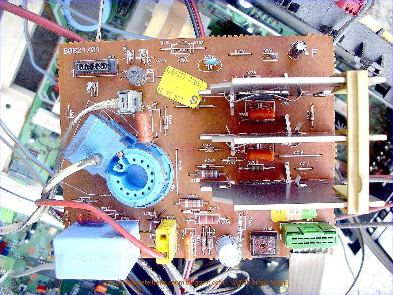
PHILIPS 28PW9608 MATCHLINE IDTV 100HZ CHASSIS FL2.24 AA Switched-mode self oscillating supply voltage circuit:POWER SUPPLY (SOPS - Self Oscillating Power Supply)
A
switched-mode self-oscillating supply voltage circuit for converting an
input voltage into an output d.c. voltage which is substantially
independent of variations of the input voltage and/or a load connected
to the output voltage. The circuit comprises a first controllable switch
connected in series with a transformer winding and a second controllable
switch for turning-off the first switch. The conduction period of the
first switch is controlled by means of a control voltage present on a
control electrode of the second switch. The circuit can be switched-over
to a stand-up state in which the energy supplied to the load is reduced
to zero. A starting network is connected between the input voltage and
the second switch so that the current therein flows through the second
switch during the period of time this switch conducts and does not flow
to the control electode of the first switch in the stand-by state.1.
A switched-mode self-oscillating supply voltage circuit for converting
an input voltage into an output d.c. voltage which is substantially
independent of variations of the input voltage and/or of a load
connected to the terminals of the output voltage, comprising a
transformer having a primary and a feedback winding, a first
controllable switch connected in series with the primary winding, the
series arrangement thus formed being coupled between terminals for the
input voltage, a second controllable switch coupled via a turn-off
capacitor to the control electrode of the first switch to turn it off,
means coupling the feedback winding to said control electrode, a
transformer winding being coupled via a rectifier to an output capacitor
having terminals which supply the output voltage, an output
voltage-dependent control voltage being present on a control electrode
of the second switch for controlling the conduction period of the first
switch, the circuit being switchable between an operating state and a
stand-by state in which relative to the operating state the supply
energy supplied to the load is considerably reduced, a starting network
connected to a terminal for the input voltage, means for adjusting the
control voltage in the stand-by state to a value at which the first
controllable switch is cut-off, a connection which carries current
during the conduction period for the second controllable switch being
provided between the starting network and said second switch, and means
providing a connection between the starting network and the control
electrode of the first switch, which connection does not carry current
in the stand-by state.
first switch, which connection does not carry current
in the stand-by state.2. A supply voltage circuit as claimed in claim 1, further comprising a resistor included between the connection of the starting network to the second switch and a turn-off capacitor present in the connection to the control electrode of the first switch.
3. A supply voltage circuit as claimed in claim 2, characterized in that the second controllable switch comprises a thyristor having a main current path included in the control electrode connection of the first controllable switch, said thyristor having a first control gate electrode for adjusting the turn-off instant of the first switch and a second control electrode to which the starting network and the resistor are connected.
4. A
supply voltage circuit as claimed in claim 1, characterized in that a
resistor is included in the connection to the control electrode of the
second controllable switch so that a current flows through said resistor
in the stand-by state of a value sufficient to cut-off the first
controllable switch.
Description:
The
invention relates to a switched-mode self-oscillating supply voltage
circuit for converting an input voltage into an output d.c. voltage
which is substantially independent of variations of the input voltage
and/or of a load connected to the terminals of the output voltage. This
circuit comprises a transformer having a primary and a feedback winding
and a first controllable switch arranged in series with the primary
winding. The series arrangement thus formed is coupled between the
terminals of the input voltage. A second controllable switch which is
coupled via a turnoff capacitor to the control electrode of the first
switch to turn it off. The feedback winding is coupled to this control
electrode and the primary winding is coupled via a rectifier to an
output capacitor the terminals of which are the terminals for the output
voltage. An output voltage-dependent control voltage is present on a
control electrode of the second switch for controlling the conduction
period of the first switch. The circuit is switchable between an
operating state and a stand-by state in which relative to the operating
state the energy supplied to the load is considerably reduced, and the
circuit further comprises a starting network connected to a terminal for
the input voltage. Such a supply voltage circuit is disclosed in German Patent Application No. 2,651,196. With this prior art circuit supply energy can be applied in the operating state to the different portions of a television receiver. In the stand-by state the majority of the output voltages of the circuit are so low that the receiver is substantially in the switched-off condition. In the prior art circuit the starting network is formed by a resistor connected to the unstabilized input voltage and through which on turn-on of the circuit a current flows via the feedback winding to the control electrode of the first controllable switch, which is a switching transistor, and brings it to and maintains it in the conductive state, as a result of which the circuit can start.
In
the stand-by state the transistor is non-conducting in a large part of
the period of the generated oscillation so that little energy is stored
in the transformer. However, the starting resistor is connected via a
diode to the second controllable switch, which is a thyristor. As the
sum of the voltages across these elements is higher than the
base-emitter threshold voltage of the transistor, the diode and the
thyristor cannot simultaneously carry current. This implies that current
flows through the starting resistor to the base of the transistor via
the feedback winding after a capacitor connected to the feedback winding
has been charged. 
The invention has for its object to provide an improved circuit of the same type in which in the stand-by state the supply energy applied to the load is reduced to zero. The prior art circuit cannot be improved in this respect without the use of mechanical switches, for example relays. According to the invention, the switched-mode self-oscillating supply voltage circuit does not comprise such relays and is characterized in that it further comprises means for adjusting the control voltage in the stand-by state to a value at which the first controllable switch is cut-off. A connection which carries current during the conduction period of the second controllable switch is provided between the starting network and said second switch while a connection present between the starting network and the control electrode of the first switch does not carry current in the stand-by state.
The invention is based on the recognition that the prior art supply voltage circuit cannot oscillate, so that the energy supplied by it is zero, if the control voltage obtains a value as referred to, while the starting network is connected in such a manner that in the stand-by state no current can flow through it to the control electrode of the first controllable switch.
It should be noted that in the said German Patent Application the starting network is in the form of a resistor which is connected to an unstabilized input d.c. voltage. It is, however, known, for example, from German Patent Specification No. 2,417,628 to employ for this purpose a rectifier network connected to an a.c. voltage from which the said input d.c. voltage is derived by rectification.

The invention will now be further described by way of example with reference to the accompanying drawing, which shows a basic circuit diagram of a switched-mode self-oscillating supply voltage circuit.
The self-oscillating supply circuit shown in the FIGURE comprises a npn-switching transistor Tr1 having its collector connected to the primary winding L1 of a transformer T, while the emitter is connected to ground via a small resistor R1, for example 1.5 Ohm. Resistor R1 is decoupled for the high frequencies by means of a 150 nF capacitor C1. One end of winding L1 is connected to a conductor which carries an unstabilized input d.c. voltage V B of, for example, 300 V. Voltage V B has a negative rail connected to ground and is derived from the electric power supply by rectification. One end of a feedback winding L2 is connected to the base of transistor Tr1 via the parallel arrangement of a small inductance L3 and a damping resistor R2. A terminal of a 47 μF capacitor C2 is connected to the junction of the elements L2, L3 and R2. The series arrangement of a diode D1 and a 2.2 Ohm-limiting resistor R3 is arranged between the other terminal of capacitor C2 and the other end of winding L2 and the series arrangement of a resistor R4 of 12 Ohm and a diode D2 is arranged between the same end of winding L2 and the emitter of transistor Tr1. A 150 nF capacitor C3 is connected in parallel with diode D2. The anode of diode D1 is connected to that end of winding L2 which is not connected to capacitor C2, while the anode of diode D2 is connected to the emitter of transistor Tr1. In the FIGURE the winding sense of windings L1 and L2 is indicated by means of dots.
The junction of capacitor C2 and resistor R3 is connected to a 100 Ohm resistor R5 and to the emitter of a pnp-transistor Tr2. The base of transistor Tr2 is connected to the other terminal of resistor R5 and to the collector of an npn-transistor Tr3, whose emitter is connected to ground. The base of Tr3 is connected to the collector of transistor Tr2. Transistors Tr2 and Tr3 form an artificial thyristor, i.e. a controllable diode whose anode is the emitter of transistor Tr2 while the cathode is the emitter of transistor Tr3. The base of transistor Tr2 is the anode gate and the base of transistor Tr3 is the cathode gate of the thyristor formed. Between the last-mentioned base and the emitter of transistor Tr1 there is arranged the series network of a 2.2 kOhm resistor R6 with the parallel arrangement of a 2.2 kOhm resistor R7 and a 100 μF capacitor C4. The series arrangement of a diode D11 and a 220 Ohm limiting resistor R19 is arranged between the junction of components R6, R7 and C4 and the junction of components C2, L2, R2 and L3. The cathode of diode D11 is connected to capacitor C2.
 Because
of the feedback the described circuit oscillates independently as soon
as the steady state is achieved. It will be described hereinafter how
this state is obtained. During the time transistor Tr1 conducts the
current flowing through the resistor R1 increases linearly. The resistor
R4 then partly determines the base current of transistor Tr1. Capacitor
C4 and resistor R7 form a voltage source the voltage of which is
subtracted from the voltage drop across resistor R1. As soon as the
voltage on the base of transistor Tr3 is equal to approximately 0.7 V
this transistor becomes conductive, as a result of which the thyristor
formed by transistors Tr2 and Tr3 becomes rapidly conductive and remains
so. Across capacitor C2 there is a negative voltage by means of which
transistor Tr1 is turned off. The inverse base current thereof flows
through thyristor Tr2, Tr3. This causes charge to be withdrawn from
capacitor C2, while the charge carriers stored in transistor Tr1 are
removed with the aid of inductance L3. As soon as the collector current
of transistor Tr1 has been turned off, the voltage across winding L2
reverses its polarity, which current recharges the capacitor. Now the
voltage at the junction of components C2, R3 and R5 is negative, causing
thyristor Tr2, Tr3 to extinguish.
Because
of the feedback the described circuit oscillates independently as soon
as the steady state is achieved. It will be described hereinafter how
this state is obtained. During the time transistor Tr1 conducts the
current flowing through the resistor R1 increases linearly. The resistor
R4 then partly determines the base current of transistor Tr1. Capacitor
C4 and resistor R7 form a voltage source the voltage of which is
subtracted from the voltage drop across resistor R1. As soon as the
voltage on the base of transistor Tr3 is equal to approximately 0.7 V
this transistor becomes conductive, as a result of which the thyristor
formed by transistors Tr2 and Tr3 becomes rapidly conductive and remains
so. Across capacitor C2 there is a negative voltage by means of which
transistor Tr1 is turned off. The inverse base current thereof flows
through thyristor Tr2, Tr3. This causes charge to be withdrawn from
capacitor C2, while the charge carriers stored in transistor Tr1 are
removed with the aid of inductance L3. As soon as the collector current
of transistor Tr1 has been turned off, the voltage across winding L2
reverses its polarity, which current recharges the capacitor. Now the
voltage at the junction of components C2, R3 and R5 is negative, causing
thyristor Tr2, Tr3 to extinguish. Secondary windings L4, L5 and L6 are provided on the core of transformer T with the indicated winding senses. When transistor Tr1 is turned off, a current which recharges a smoothing capacitor C5, C6 or C7 via a rectifier D3, D4 or D5 flows through each of these windings. The voltages across these capacitors are the output voltages of the supply circuit for loads connectable thereto. These loads, which are not sho
wn in the FIGURE, are, for example, portions of a television receiver. In parallel with winding L1 there is the series network of a 2.2 nF tuning capacitor C8 and a 100 Ohm limiting resistor R8. The anode of a diode D6 is connected to the junction of components R8 and C8, while the cathode is connected to the other terminal of resistor R8. Winding L1 and capacitor C8 form a resonant circuit across which an oscillation is produced after windings L4, L5 and L6 have become currentless. At a later instant the current through circuit L1, C8 reverses its direction. As a result thereof a current is generated in winding L2 which flows via diode D2 and resistor R4 to the base of transistor Tr1 and makes this transistor conductive and maintains it in this state. The dissipation in resistor R8 is reduced by means of diode D6. A clamping network formed by the parallel arrangement of a 22 kOhm resistor R9 and a 120 nF capacitor C9 is arranged in series with a diode D7. This whole assembly is in parallel with winding L1 and cuts-off parasitic oscillations which would be produced during the period of time in which transistor Tr1 is non-conductive. The output voltages of the supply circuit are kept substantially constant in spite of variations of voltage V B and/or the loads, thanks to a control of the turning-on instant of thyrisistor Tr2, Tr3. For this purpose the emitter of a light-sensitive transistor Tr4 is connected to the base of transistor Tr3. The collector of transistor Tr4 is connected via a resistor R10 to the conductor which carries the voltage V B and to a Zener diode Z1 which has a positive voltage of approximately 7.5 V, while the base is unconnected. The other end of diode Z1 is connected to ground. A light-emitting diode D8, whose cathode is connected to the collector of an npn-transistor Tr5, is optically coupled to transistor Tr4. By means of a potentiometer R11 the base of transistor Tr5 can be adjusted to a d.c. voltage which is derived from the voltage V 0 of approximately 130 V across capacitor C6. The anode of diode D8 is connected to a d.c. voltage V 1 of approximately 13 V. A resistor R12 is also connected to voltage V 1 , the other end of the resistor being connected to the emitter of transistor Tr5, to the cathode of a Zener diode Z2 which has a voltage of
approximately 7.5 V and to a smoothing capacitor C10. The other ends
of diode Z2 and capacitor C10 are connected to ground. Voltage V1 can be
generated by means of a transformer connected to the electric AC supply
and a rectifier, which are not shown for the sake of simplicity, more
specifically for a remote control to which constantly supply energy is
always applied, even when the majority of the components of the receiver
in what is referred to as the stand-by state are not supplied with
supply energy. A portion of voltage V 0 is compared with the voltage of diode Z2 by means of transistor Tr5. The measured difference determines the collector current of transistor Tr5 and consequently the emitter current of transistor Tr4. This emitter current produces across resistor R6 a voltage drop whose polarity is the opposite of the polarity of the voltage source formed by resistor R7 and capacitor C4. Under the influence of this voltage drop the turn-on instant of thyristor Tr2, Tr3 is controlled as a function of voltage V 0 . If, for example, voltage V 0 tends to decrease owing to an increasing load thereon and/or in response to a decrease in voltage V B , then the collector current of transistor Tr5 decreases and consequently also the said voltage drop. Thyristor Tr2, Tr3 is turned on at a later instant than would otherwise be the case, causing transistor Tr1 to be cut-off at a later instant. The final value of the collector current of this transistor is consequently higher. Consequently, the ratio of the time interval in which transistor
Tr1 is conductive to the entire period, commonly referred to as the duty cycle, increases, while the frequency decreases. The circuit is protected from overvoltage. This is ensured by a thyristor which is formed by a pnp-transistor Tr6 and an npn-transistor Tr7. The anode of a diode D9 is connected to the junction of components R3 and C2 and the cathode to the base of transistor Tr6 and to the collector of transistor Tr7. The base of transistor Tr7, which base is connected to the collector of transistor Tr6, is connected via a zener diode Z3 to a voltage which, by means of a potentiometer R13 is adjusted to a value derived from the voltage across capacitor C7. The emitter of transistor Tr6 also is connected to the voltage of capacitor C7, more specifically via a resistor R14 and a diode D10. If this voltage increases to above a predetermined value then thyristor Tr6, Tr7 becomes conductive. Since the emitter of transistor Tr7 is connected to ground, the voltage at its collector becomes very low, as a result of which diode D9 becomes conductive, which keeps transistor Tr1 in the non-conducting state. This situation is maintained as long as thyristor Tr6, Tr7 continues to conduct. This conduction time is predominantly determined by the values of capacitor C7, resistor R14 and a resistor R15 connected between the base and the emitter of transistor Tr6. A thyristor is advantageously used here to render it possible to switch off a large current even with a low level signal and to obtain the required hysteresis.
The
circuit comprises a 1 MOhm starting resistor R16, one end of which is
connected to the base of transistor Tr2 and the other end to the
conductor which carries the voltage V B . Upon turn-on of the
circuit current flows through resistors R16 and R5 and through
capacitor C2, which has as yet no charge, to the base of transistor Tr1.
The voltage drop thus produced across resistor R5 keeps transistor Tr2,
and consequently also transistor Tr3, in the non-conductive state,
while transistor Tr1 is made conductive and is maintained so by this
current. Current also flows through winding L2. In this manner the
circuit can start as energy is built up in transformer T. The supply circuit can be brought into the stand-by state by making an npn-transistor Tr8, which is non-conductive in the operating state, conductive. The emitter of transistor Tr8 is connected to ground while the collector is connected to the collector of transistor Tr5 via a 1.8 kOhm resistor R17. A resistor R18 has one end connected to the base of transistor Tr8 and the other end, either in the operating state to ground, or in the stand-by state to a positive voltage of, for example, 5 V. Transistor Tr8 conducts in response to this voltage. An additional, large current flows through diode D8 and consequently also through transistor Tr4, resulting in thyristor Tr2, Tr3 being made conductive and transistor Tr1 being made non-conductive and maintained so. So to all appearances a large control current is obtained causing the duty cycle to be reduced to zero. A condition for a correct operation is that the emitter current of transistor Tr4 be sufficiently large in all circumstances, which implies that the voltage drop produced across resistor R6 by this current is always higher than the sum of the voltage across voltage source R7, C4, of the base-emitter threshold voltage of transistor Tr3 in the conductive state thereof, and of the voltage at the emitter of transistor Tr1. So the said voltage drop must be higher than the sum of the first two voltages, which corresponds to the worst dimensioning case in which the stand-by state is initiated while transistor Tr1 is in the non-conductive state.
If thyristor Tr2,
Tr3 conducts, either in the operating state or in the stand-by state,
current flows through resistor R16 via the collector emitter path of
transistor Tr3 to ground. This current is too small to have any
appreciable influence on the behaviour of the circuit. When thyristor
Tr2, Tr3 does not conduct, the voltage on the left hand terminal of
capacitor C2 is equal to approximately 1 V, while the voltage across the
capacitor is approximately -4 V. So transistor Tr1 remains in the
non-conductive state and a premature turn-on thereof cannot occur. If in
the operating state transistor Tr1 conducts while thyristor Tr2, Tr3 is
cut-off, then the current flows through resistor R16 in the same manner
as it flows during the start to the base of transistor Tr1, but has
relatively little influence as the base current caused by the energy
stored in winding L2 is many times larger. If both transistor Tr1 and
thyristor Tr2, Tr3 are non-conductive, then the current through resistor
R16 flows through components R5, C2, L2, R4, C3 and R1. In this
stand-by state capacitor C2 has indeed substantially no negative charge
any longer but, in spite thereof, transistor Tr1 cannot become
conductive since no current flows to its base. It will furthermore be
noted that the circuit is protected in the event that thyristor Tr2, Tr3
has an interruption. Namely, in such a case the circuit cannot start. In the foregoing a circuit is described which may be considered to be a switched-mode supply voltage circuit of the parallel ("flyback") type. It will be obvious that the invention may alternatively be used in supply voltage circuits of a different type, for example converters of the type commonly referred to as up-converters. It will also be obvious that transistor Tr1 may be replaced by an equivalent switch, for example a gate-turn-off switch.
TDA8425 Hi-fi stereo audio processor;I2C-bus
GENERAL DESCRIPTIONThe TDA8425 is a monolithic bipolar integrated stereo sound circuit with a loudspeaker channel facility, digitally
controlled via the I2C-bus for application in hi-fi audio and television sound.
Feature:
· Source and mode selector for two stereo channels
· Pseudo stereo, spatial stereo, linear stereo and forced mono switch
· Volume and balance control
· Bass, treble and mute control
· Power supply with power-on reset
FUNCTIONAL DESCRIPTION
Source selector
The input to channel 1 (CH1) and channel 2 (CH2) is determined by the source selector. The selection is made from the
following AF input signals:
· IN 1 L (pin 18); IN1 R (pin 20)
or
· IN2 L (pin 1); IN2 R (pin 3)
Mode selector
The mode selector selects between stereo, sound A and sound B (in the event of bilingual transmission) for OUT R and
OUT L.
Volume control and balance
The volume control consists of two stages (left and right). In each part the gain can be adjusted between +6 dB and
-64 dB in steps of 2 dB. An additional step allows an attenuation of ³ 80 dB. Both parts can be controlled independently
over the whole range, which allows the balance to be varied by controlling the volume of left and right output channels.
Linear stereo, pseudo stereo, spatial stereo and forced mono mode(1)
It is possible to select four modes: linear stereo, pseudo stereo, spatial stereo or forced mono. The pseudo stereo mode
handles mono transmissions, the spatial stereo mode handles stereo transmissions and the forced mono can be used
in the event of stereo signals.
Bass control
The bass control stage can be switched from an emphasis of 15 dB to an attenuation of 12 dB for low frequencies in
steps of 3 dB.
Treble control
The treble control stage can be switched from +12 dB to -12 dB in steps of 3 dB.
Bias and power supply
The TDA8425 includes a bias and power supply stage, which generates a voltage of 0.5 ´ VCC with a low output
impedance and injector currents for the logic part.
Power-on reset
The on-chip power-on reset circuit sets the mute bit to active, which mutes both parts of the treble amplifier. The muting
can be switched by transmission of the mute bit.
I2C-bus receiver and data handling
Bus specification
The TDA8425 is controlled via the 2-wire I2C-bus by a microcomputer.
The two wires (SDA - serial data, SCL - serial clock) carry information between the devices connected to the bus. Both
SDA and SCL are bidirectional lines, connected to a positive supply voltage via a pull up resistor.
When the bus is free both lines are HIGH.
The data on the SDA line must be stable during the HIGH period of the clock. The HIGH or LOW state of the data line
can only change when the clock signal on the SCL line is LOW. The set up and hold times are specified in AC
CHARACTERISTICS.
A HIGH-to-LOW transition of the SDA line while SCL is HIGH is defined as a start condition.
A LOW-to-HIGH transition of the SDA line while SCL is HIGH is defined as a stop condition.
The bus receiver will be reset by the reception of a start condition. The bus is considered to be busy after the start
condition.
The bus is considered to be free again after a stop condition.
Module address
Data transmission to the TDA8425 starts with the module address MAD.
PHILIPS 28PW9608 MATCHLINE IDTV 100HZ CHASSIS FL2.24 AA Rapid access teletext - Videotextx decoder arrangement:A teletext decoder includes a background or buffer memory operating as a first-in, first-out (
FIFO)
memory. The buffer memory is used for storing a large number of
teletext pages. A given video line that contains teletext information
is identified as such by the detection of part of a clock run-in
sequence followed by the framing code. The video line is then stored in
the background memory. After a user page request occurs, the
background memory is read-out by a data processor operating in a full
channel mode of operation for obtaining the information of the
requested page. As long as the read-out operation has not been
terminated, incoming teletext data is stored in the background memory.
This enables teletext data received prior to termination of the read-out
operation to be read out and processed by the data processor. 1. A television apparatus responsive to an incoming television signal containing video lines that carry text data, defining corresponding data lines, for generating an output signal that is capable of providing picture information to a display device, comprising:
means for generating a first control signal in order to select one of said data lines to be used in conjunction with the generation of said output signal;
a source of said television signal;
a first-in, first-out background memory having a data input that is coupled to an output of said source;
first
control means coupled to said background memory for controlling
storage therein of corresponding data lines of said television signal,
wherein prior to the time said first control signal is generated, said
background memory already contains a substantial number of stored data
lines of said television signal; second control means responsive to said first control signal and coupled to said background memory for controlling during a given interval that follows the generation of said first control signal, read-out from said background memory of a plurality of data lines of said television signal that have been stored before the end of said given interval, said given interval having a duration that is substantially shorter than that of a corresponding interval between the occurrence of an initial data line of said plurality of data lines and the occurrence of a final data line thereof so as to reduce access time to said plurality of data lines, said second control means controlling read-out of said plurality of data lines in a first-in, first-out manner for generating during said given interval a data signal that contains the data of said plurality of data lines including data lines that have been stored in said background memory during said given interval; and
a data processor responsive to said data signal for selecting said one data line to generate in accordance therewith said output signal.
2. An
apparatus according to claim 1 wherein said data lines occur in said
television signal only during, corresponding vertical blanking
intervals, wherein, during said given interval, said data processor
operates in a full channel mode of operation, and wherein, prior to the
time when said first control signal is generated, said data processor
operates in a field flyback mode of operation.
3. An apparatus according to claim 1 further comprising,
means for coupling said data signal and said television signal to said
data processor such that prior to the time said first control signal is
generated said television signal is coupled to said data processor in a
manner that bypasses said background memory.
4. An apparatus according to claim 3 wherein, throughout
said given interval, said coupling means decouples said signal that
bypasses said background memory from said data processor.
5. An apparatus according to claim 1 further
comprising, a switch having a first input that is coupled between said
output of said source of said television signal and said data input of
said background memory, a second input that is coupled to a data output
of said background memory and a switch output that is coupled to an
input of said data processor. 6.
An apparatus according to claim 5 further comprising, means for
generating a second control signal that is coupled to a control input
of said switch, said second control signal having a first state for
enabling said switch to couple the signal that is developed at said
second input of said switch to said data processor following the time
when said first control signal is generated and having a second state,
for enabling said switch to couple the signal that is developed at said
first input thereof to said data processor following the occurrence of
the earlier of (a) a time when all the data stored in said background
memory has been read out, and (b) a time when a first time-out interval
has elapsed from a time when said data processor selects the data of a
Page Header data line. 7. An
apparatus according to claim 5 further comprising, means coupled to
said background memory, for generating, in accordance with the data of
said plurality of data lines, a serial bit data signal that contains
corresponding data lines that are read out of said background memory in
a first-in, first-out manner, said serial bit data signal being
coupled to said second input of said switch, said switch coupling said
serial bit data signal to said input of said data processor, during
said given interval, and coupling the signal that is developed at said
first input of said switch to said input of said data processor, outside
said given interval. 8. An
apparatus according to claim 1 wherein, as a result of reading out the
data of said plurality of data lines in the first-in, first-out manner,
memory addresses, where said plurality of data lines are stored in
said background memory are transparent to the operation of said data
processor. 9. An apparatus
according to claim 1 wherein said data processor is included in an
integrated circuit of the same type used in a conventional teletext
decoder such that said background memory provides an add-on feature.
10. An apparatus according to claim 1
wherein said television signal comprises a teletext signal and wherein
said television apparatus comprises a teletext decoder.
11. An apparatus according to claim 10 wherein
said data lines of said television signal define corresponding pages of
teletext data, wherein said background memory is capable of containing
at a given time the data of a substantial number of said pages and
wherein, during said given interval, said data processor selects from
the data that is read out of said background memory the data of a first
page, in accordance with said one of said data lines that is a
Page-Header data line, to generate from the data of said first page
said output signal. 12. An
apparatus according to claim 1 further comprising, a page memory
wherein said output signal is stored in said page memory during said
given interval. 13. An apparatus
according to claim 1 further comprising, a switch for coupling one of
said data signal that is generated at an output of said background
memory and a second data signal, that bypasses said background memory,
to an input of said data processor when a second control signal that is
developed at a control input of said switch is at first state and for
coupling the other one of said to said input of said data processor
when said second control signal is at a second state.
14. An apparatus according to claim 13 further
comprising, means for generating, during said given interval, a first
time-out signal after an interval having a predetermined duration has
elapsed from a time when the data of said one of said data line that is
a Page Header data line has been identified in said data signal and
means responsive to said first time-out signal for generating said
second control signal in accordance with said first time-out signal .
15. An apparatus according to
claim 13 further comprising, means for generating a signal that is
indicative
of when the data of all the da&a lines that are stored in said
background memory have been read out and that is coupled to said
control input of said switch to control the state of said second
control signal. 16. A television
apparatus according to claim 1 wherein said data processor is
responsive, outside said given interval, to data lines of said
television signal that are coupled to said data processor in a manner
that bypasses said background memory.
17. An apparatus according to claim 1 further comprising, a
parallel-to-serial converter that is coupled between an output of said
background memory and an input of said data processor.
18. A television apparatus according to claim 1
wherein said background memory comprises a random access memory,
wherein said first control means comprises first sequencing means that
is coupled to an address input of said random access memory for
generating a write-in address word and wherein said second control
means comprises second sequencing means for generating a read-out
address word that is coupled to said address input.
19. An apparatus according to claim 18 wherein at
least one of said first and second sequencing means comprises a linear
feedback shift register counter.
20. An apparatus according to claim 18 wherein each of said data lines
includes a corresponding plurality of data line portions that are
stored in corresponding locations in said background memory having
corresponding addresses, wherein said first sequencing means changes
states in a cyclical manner each time a given one of said portions of
each data line is stored such that the number of states in each cycle is
equal to an integer multiple of the total number of data lines that
can be stored in said background memory in each cycle.
21. An apparatus according to claim 20 wherein
the number of memory addresses that are required for storing a given
data line is equal to 86. 22. An
apparatus according to claim 20 wherein the number of said states in
each cycle is equal to. 23. A
television apparatus according to claim 1 further comprising, a page
memory responsive to said output signal for storing said output signal
therein. 24. An apparatus
according to claim 1 wherein said data processor operates in a full
channel mode of operation throughout said given interval and wherein
said television signal contains said data lines only during
corresponding vertical blanking intervals thereof.
25. An apparatus according to claim 1 wherein said
first control means identifies, in a given video line signal, data of a
clock run-in portion of said video line signal and stores in said
background memory text data of such video line signal provided that
said data of said clock run-in portion is identified.
26. An apparatus according to claim 25 wherein said
said first control means identifies said given data line also in
accordance with data of a framing code.
27. An apparatus according to claim 1 wherein said first control
signal is indicative of when a user initiated page request has occurred
and causes said data processor to operate in a full channel mode of
operation during said given interval.
28. An apparatus according to claim 27 further comprising, means
for generating a second control signal that is indicative when a
predetermined time-out interval has elapsed from the time said first
control signal is generated, said second control signal being coupled to
said data processor for causing said data processor to start operating
in a field flyback mode of operation following said time-out interval
irrespective of whether said one of said data lines that is a Page
Header of the page requested has been selected.
29. An apparatus according to claim 28 wherein said
second control signal is generated in a microprocessor such that said
time out interval is determined by a program thereof.
30. A television apparatus responsive to an
incoming television signal containing video line signals that carry
text data, defining corresponding data lines, for generating an output
signal that is capable of providing picture information to a display
device, comprising: means for generating a first control signal
in order to select one of said data lines to be used in conjunction
with the generation of said output signal; a source of said television signal;
a first-in, first-out background memory having a data input that is coupled to said source;
first control means coupled to said background memory for controlling storage therein of corresponding data lines of said television signal, wherein prior to the time said first control signal is generated, said background memory already contains a substantial number of stored data lines of said television signal;
second control means responsive to said first control signal and coupled to said background memory for controlling during a given interval that follows the generation of said first control signal, read-out from said background memory of a plurality of stored data lines of said television signal, such that the duration of said given interval is substantially shorter than that of a corresponding interval between the occurrence of an initial data line of said plurality of data lines and the occurrence of a final data line thereof, so as to reduce access time to said plurality of data lines, said second control means controlling read-out of said plurality of data lines in a first-in, first-out manner for generating during said given interval a data signal that contains the data of said plurality of data lines;
a switch having a first input that is coupled to said source of said television signal, having a second input that is coupled to a data output of said background memory and having an output for generating a second data signal;
a data processor responsive to said second data signal for selecting said one data line to generate in accordance therewith said output signal; and
means for generating a second control signal that is coupled to a control input of said switch, said second control signal having a first state for enabling said switch to couple to said data processor after said first control signal is generated the signal that is developed at said switch second input, and having a second state for enabling said switch to couple to said data processor the signal that is developed at said first switch input following the occurrence of the earlier of (a) a time when all the data stored in said background memory has been read out, and (b) a time when a time-out interval has elapsed from a time when said data processor selects said one data line that is a Page Header.
31. A television apparatus responsive to an incoming television signal containing video lines that carry text data, defining corresponding data lines, for generating an output signal that is capable of providing picture information to a display device, comprising:
first means for generating a first control signal in order to select one of said data lines to be used in conjunction with the generation of said output signal;
second means responsive to said television signal for generating a clock signal that is indicative of timings of individual bits of a data sequence of a clock run-in portion of a data line;
a source of said television signal;
a first-in, first-out background memory having a data input that is coupled to said source;
third means coupled to said background memory and responsive to said television signal and to said clock signal for identifying in a given video line, said data sequence of said clock run-in portion of said data line and for storing in said background memory such video lines that are identified as data lines but only when individual bits of said data sequence of said clock run-in portion are correct, said first means storing said data lines such that prior to the generation of said first control signal, said background memory already contains a substantial number of stored data lines of said television signal;
fourth means responsive to said first control signal and coupled to said background memory for controlling during a given interval that follows the generation of said first control signal, read-out from said background memory of a plurality of stored data lines of said television signal, suc
h that the duration of said given interval is substantially
shorter than that of a corresponding interval between the occurrence
of an initial data line of said plurality of data lines and the
occurrence of a final data line thereof, so as to reduce access time to
said plurality of data lines, said fourth means controlling read-out
of said plurality of data lines in a first-in, first-out manner for
generating during said given interval, a data signal that contains the
data of said plurality of data lines; and a data processor responsive to said data signal for selecting said one data line to generate in accordance therewith said output signal.
32. An apparatus according to claim 31 wherein said third means identifies said video line as data line when data sequence of a framing code portion immediately follows said data sequence of said clock run-in portion. 33. An apparatus according to claim 31 wherein said third means identifies said video line as data line by identifying a 12 bit sequence (101011100100) in data that are derived from said video line.
Description:
This
invention relates to a teletext decoder employing a so-called
background or buffer memory for storing multipages of teletext incoming
data. Teletext is a television-based communication technique in which a given horizontal video line is utilized for broadcasting textual and graphical information encoded in a digital binary representation. Such horizontal video line signal that contains teletext data is referred to herein as a Data-line. It is assumed herein, for explanation purposes, that teletext is sent by the broadcaster only during the vertical blanking interval (VBI), when no other picture information is sent. The organization of the binary information in the broadcast signal is determined by the standard employed by the broadcaster. By way of an example only, references are made herein to a teletext based on a standard referred to by the British Broadcasting Corporation (BBC) as CEEFAX.
Each Data-line carries data synchronizing and address information and the codes for a Row of 40 characters. The synchronizing information includes a clock run-in sequence followed by an 8-bit framing code sequence. Each Data-line contains a 3 bit code referred to as the Magazine number. A teletext Page includes 24 Rows of 40 characters, including a special top Row called the Page-Header. Each ROW is contained in a corresponding Data-line. A user selected Page is intended to be displayed in place of, or added to a corresponding television picture frame. A Magazine is defined to include Pages having Data-lines containing a corresponding Magazine number. The transmission of a selected Page begins with, and includes its Page Header and ends with and excludes the next Page Header of the selected Magazine number. All intermediate Data lines carrying the selected Magazine number relate to the selected Page.
 FIG.
1 illustrates a block diagram of a conventional teletext decoder that
includes an integrated circuit (IC) referred to herein as video input
processor (VIP) such as, for example, of the type SAA5231 made by
Philips Corporation. The VIP receives a baseband composite video signal
VIDEO that contains Data-lines. The VIP performs data slicing, clock
regeneration and timing synchronization functions and generates a serial
data signal DATA and an associated clock signal CLOCK Signals DATA and
CLOCK represent the data contained in the horizontal video lines.
Signals DATA and CLOCK are coupled to a second IC of the decoder,
referred to herein as computer controlled teletext IC (CCT) that
includes a data processor responsive to signals DATA and CLOCK. An
example of such CCT is IC SAA5243 made by Philips Corporation.
FIG.
1 illustrates a block diagram of a conventional teletext decoder that
includes an integrated circuit (IC) referred to herein as video input
processor (VIP) such as, for example, of the type SAA5231 made by
Philips Corporation. The VIP receives a baseband composite video signal
VIDEO that contains Data-lines. The VIP performs data slicing, clock
regeneration and timing synchronization functions and generates a serial
data signal DATA and an associated clock signal CLOCK Signals DATA and
CLOCK represent the data contained in the horizontal video lines.
Signals DATA and CLOCK are coupled to a second IC of the decoder,
referred to herein as computer controlled teletext IC (CCT) that
includes a data processor responsive to signals DATA and CLOCK. An
example of such CCT is IC SAA5243 made by Philips Corporation. The CCT performs data acquisition and interface function with a page memory that is included in the teletext decoder. For example, only a teletext Page requested by the user is derived by the CCT from the serial data and clock signals and stored in the page memory. The CCT also generates video display signals R,G, and B from the teletext data stored in the page memory to provide corresponding drive signals that contain picture information for display in the receiver picture tube (CRT), not shown.
A control microcomputer, not shown in FIG. 1, that is responsive to user initiated commands, generates control and status messages. The messages are coupled via, for example, a standard IIC bus to the CCT, for controlling the operation of the CCT.
A total of, for example, 500 Pages may be periodically transmitted during each interval of 15-45 seconds, depending on the number of Data-lines used for teletext during the VBI. Consequently, if the teletext Page is not already stored in memory when a new user page request occurs, the user may experience a nuisance as a result of waiting a maximum of 15-45 seconds until the requested Page is displayed. It may be desirable to reduce such Page access time. It may also be desirable to utilize in the teletext decoder a standard CCT such that the reduction of the access time is provided as an add-on feature to the teletext decoder.
A teletext decoder, embodying an aspect of the invention, includes a background or buffer memory that is capable of storing multi-Pages of teletext data. The portion of serial data signal DATA generated by the VIP that meets a predetermined identification criteria and, therefore, assumed to represent a Data-line is stored in the buffer memory. At any given time after the operation of the buffer memory is enabled, such as immediately after the user turns on the television receiver, the buffer memory contains, for example, the most recently received teletext Pages. The maximum number of such Pages that can be contained in the buffer memory at any given time is determined by the buffer memory Page storage capacity.
In order to reduce the size of the hardware required to identify each video line that is assumed to be a Data-line, only a limited, rather than a complete identification operation, is initially performed. The complete identification is accomplished in the CCT, during a read-out operation, when the data is read-out of the buffer memory.
In
accordance with a feature of the invention, the limited identification
operation for identifying a given Data-line is accomplished by
identifying in a video line signal data of a sequence of the clock
run-in that is immediately followed by a sequence of the framing code.
When, for example, both sequences are identified it is assumed that a
Data-line is identified. Therefore, a portion of such identified
Data-line that contains relevant data bits is stored in the buffer
memory. Otherwise, the video line information is not stored in the
buffer memory. The inclusion of the test for the data of the clock
run-in sequence, advantageously, reduces the probability that the data
that is stored is, in fact, not a Data-line. When the user's page request occurs, the data processor of the CCT receives the data that have been stored in the buffer memory and searches for the presence of a Data-line representing a Page Header of the requested Page. The search operation that is included in the read-out operation begins when the first data is read out of the buffer memory following the occurrence of the user's page request.
Memory read-out cycles occur between VBI's, when no teletext data is received. If the Page Header of the user requested teletext Page is found in the buffer memory in the course of such memory scan or search operation, the stored data of the Page Header is transferred to the page memory.
During the search operation, the CCT operates in the full channel operation mode. In the full channel operation mode, the Data-lines in the buffer memory are read out and transferred to the page memory in a first-in, first-out manner and without encountering large time gaps. Such large time gaps occur when teletext information is received by th
e CCT only
during the VBI's. Therefore, the search operation occurs faster than if
the Data lines were received, unbuffered, only during the VBI's. For
example, the access time to a teletext Page that is already contained
in a buffer memory capable of storing 500 teletext Pages may be reduced
to, for example, 0.8 seconds that is, advantageously, substantially
shorter than the 15-45 seconds maximum access time, referred to before.
Furthermore, should more than, for example, 600 pages be transmitted,
the access time for a page which, at the time the user page request
occurs, is not already stored in the memory, is reduced by the time
required to fill the buffer memory with teletext data. After the Page Header is identified in the CCT, other Data-lines that are associated with the requested Page and that are stored in the buffer memory are read-out. On the other hand, if no Page Header Data-line of the requested teletext Page is found in the buffer memory in the course of the search operation, the unbuffered data received from the VIP will be coupled, after the end of the search operation, directly to the data processor of the CCT such that the buffer memory is bypassed.
When a buffer memory with large storage capacity is utilized, the read-out operation that was explained before may require a longer interval than the interval between consecutive VBI's. It may be desirable to store incoming Data-lines in the buffer memory that occur during the intervening VBI's prior to the completion of the read-out operation. If such incoming Data-lines of the Page requested by the user were not stored, an undesirable situation might have occurred in which only a partial Page is temporarily displayed on the CRT. Such temporary condition may continue until after the time when the same Page is re-transmitted.
In the teletext decoder, embodying an aspect of
the invention, the read-out operation in the buffer memory occurs only
outside the VBI's. Data-lines are stored in the buffer memory during
the VBI's that occur prior to the completion time of the read-out
operation. Therefore, Data-lines that were stored in the buffer memory
after the read-out operation has been initiated and prior to its
termination may be read-out and processed by the CCT. In this way,
advantageously an incoming Data-line that is included in the teletext
Page that is requested may be processed during the read-out operation Each Data-line is stored in the background memory and provided to the CCT in a format that can be readily processed by the CCT. For example, a Data-line is stored as 344 bits that include a byte containing the framing code, two bytes containing hamming codes and forty bytes containing the remaining data.
The buffer memory of the decoder of the invention is organized as a serial memory such as, for example, a first-in, first-out memory (FIFO). For example, immediately after teletext signal is received in the television receiver, the Data-lines are stored in the FIFO even if no user page request occurs. Thus, at the time the user changes the mode of operation of the television receiver from providing normal picture program to providing teletext information, the most recently received teletext data are already stored in the buffer memory.
The buffer memory may utilize, advantageously, a dynamic random access memory (DRAM) of a large capacity that operates as a FIFO. The DRAM may be refreshed between VBI's. A given storage location of the FIFO may be addressed by a read address pointer during the memory read-out operation and by a write address pointer during the VBI's when memory store-in operation occurs. By using separate read and write address pointers, the aforementioned advantage of storing Data-lines while the read-out operation is incomplete may be realized.
A television apparatus, embodying an aspect of the invention, is responsive t
o an incoming television
signal containing video lines that carry text data, defining
corresponding data lines for generating an output signal that is
capable of providing picture information to a display device. A first
control signal is generated in order to select one of the data lines to
be used in conjunction with the generation of the output signal. A
first-in, first-out background memory has a data input that is coupled
to an output of a source of the television signal. Storage of
corresponding data lines of the television signal in the background
memory occurs each time such corresponding data lines occur. Prior to
the time the first control signal is generated, the background memory
already contains a substantial number of stored data lines of the
television signal. During a given interval that follows the generation
of the first control signal, read-out from the background memory of a
plurality of data lines of the television signal that have been stored
before the end of the given interval occurs. The given interval has a
duration that is substantially shorter than that of a corresponding
interval between the occurrence of the first one of the plurality of
data lines and the occurrence of the last one so as to reduce access
time to the plurality of data lines. Read-out of the plurality of data
lines occurs in a first-in, first-out manner for generating during the
given interval a data signal that contains the data of the plurality of
data lines, including data lines that have been stored in the
background memory during the given interval. A data processor is
responsive to the data signal for selecting the one data line to
generate in accordance therewith the output signal. FIG. 1 illustrates a prior art teletext decoder;
FIG. 2 illustrates a rapid access teletext decoder, embodying a feature of the invention;
FIG. 3 illustrates a diagram that is useful for explaining the operation of a first-in, first-out background memory of FIG. 2;
FIG. 4 illustrates a flow chart that is useful for explaining the operation of the teletext decoder of FIG. 2; and
FIG. 5 illustrates a detail schematic of a linear feedback shift register that is used to provide an address pointer for a background memory of FIG. 2.
 FIG.
2 illustrates a block diagram of a rapid access teletext decoder,
embodying an aspect of an invention. Similar symbols and numerals in
FIGS. 1 and 2 indicate similar items or functions.
FIG.
2 illustrates a block diagram of a rapid access teletext decoder,
embodying an aspect of an invention. Similar symbols and numerals in
FIGS. 1 and 2 indicate similar items or functions. A baseband composite video signal VIDEO of FIGURE 2 is coupled from a video detector, not shown, to a VIP 20, such as, for example, of the type SAA5231. VIP 20 generates from signal VIDEO a serial data signal TTDout at a bit rate of 6.9375 MHz and a corresponding clock signal CLOCK that provides timing information of the bits of signal TTDout. VIP 20 also generates a video composite sync signal VCS derived from signal VIDEO. Signal VCS is coupled to a CCT 30 such as, for example, of the SAA5243 IC type. In turn, CCT 30 generates a signal SAND containing the phase locking and color burst blanking information. Signal SAND is coupled back to VIP 20 to provide horizontal phase-locking information to an oscillator of VIP 20, not shown.
The serial data contained in signal TTDout are coupled to a serial-to-parallel converter 35 that includes a shift register, not shown. Serial-to-parallel converter 35 generates a parallel word 35a that is coupled to an identification unit 40.
In accordance with an aspect of the invention, unit 40 tests for the occurrence, in signal TTDout, of a 12-bit sequence (101011100100) of bits in the data stream, representing a 4-bit clock run-in sequence immediately followed by the framing code. The checking for the occurrence of such 12-bit sequence is performed during a time window of 2.7 microsecond, starting 11.8 microseconds after the leading edge of a horizontal sync portion, not shown, of signal VIDEO. Such checking is done for each video line during the possible teletext lines, 6-22 and 319-335, that occur in the VBI's of the corresponding field portions of signal VIDEO.
When the 12-bit sequence is recognized, it is assumed that the video line represents a Data-line of teletext. After an assumed Data-line is identified, only, for example, 344 bits of the assumed data-line are stored in a buffer memory 45, operating as a FIFO. Advantageously, the checking for the 4-bit clock run-in sequence reduces a probability that nonteletext data of a video line that is not a Data-line will be stored in memory 45.
A timing and control unit 100 receives signals SAND, VCS and CLOCK and generates corresponding control signals that, for example, control the operations associated with memory 45, such as the operation of identification unit 40.
It may be desirable to utilize a DRAM IC of a large storage capacity such as, for example, of the 1,098,586 (2 20 ) bit organization as the main storage element of buffer memory 45. This is so in order to provide a storage capacity for a substantial number of teletext Pages. Also, in order to reduce the cost and power dissipation of memory 45 it may be desirable to utilize DRAM's with slow access or cycle time that are typically less expensive. Therefore, the serial teletext data in signal TTDout is converted by converter 35 to 4-bit parallel words, or nibbles 35b. The bits of each nibble 35b are stored simultaneously in buffer memory 45, organized as, for example, a four-bit-wide DRAM. In this way, the DRAM cycle time may be longer than the teletext bit rate.
For each assumed Data-line, the nibble that is firstly stored in buffer memory 45 corresponds to the most significant nibble of the framing code. Thereafter, the remaining consecutively occurring 85 nibbles are stored. The clock run-in bits need not be stored.
A write counter 55 generates a write address pointer, or word W-COUNT that is coupled via a multiplexer/comparator 60 to an address port 45a of memory 45. FIG. 5 illustrates a combination of a schematic diagram and a block diagram of counter 55 of FIG. 2. Similar numerals and symbols in FIGS. 2 and 5 indicate similar items or functions.
Write counter 55 of FIG. 5 includes a 6-bit conventional binary counter 551 that produces 6 bits, A0-A5, of word W-COUNT. The most significant bit of counter 551, bit A5, is coupled to a corresponding clock input terminal CP of each flip-flop of a conventional 14-bit linear feedback shift register (LFSR) counter 552. Counter 552 includes 14 D-type flip-flops that form a shift register The input to a data input terminal of a first flip-flop 552a in the shift register chain of the flip-flops is formed by applying suitable EXCLUSIVE 0R operations on output signals of the first, third, fifth and fourteenth flip-flops in the shift register chain, in a well known manner.
LFSR counter
552 requires less hardware and is faster than a conventional binary
counter since it avoids the carry propagation associated with the
conventional binary counter. LFSR counter 552 goes through a complete
sequence cycle every 2 14 -1 pulses of bit A5 of binary counter 551. Binary counter 551 goes through a complete sequence cycle every 2 6
clock pulses at an input terminal 551a of counter 551. Consequently,
each of counter 55 and word W-COUNT sequences through a complete
predetermined cyclical sequence every 2 20 -64 clock pulses that occur at input terminal 551a. The address of each nibble that is stored is supplied by word W-COUNT of counter 55 of FIG. 2. The value of word W-COUNT is changed to the next or consecutive value in the predetermined cyclical sequence of counter 55 after each nibble is stored. The number of different values in such cyclical sequence that is, for example, (2 20 -64), is equal to the number of nibble storage locations utilized in memory 45. Therefore, advantageously, each DRAM, having 2 20 locations, is substantially fully utilized. The number (2 20 -64) is equal to an integer multiple of 86, the number of nibbles required for storing the 344 bits of each Data-line. As a result of the FIFO operation, a maximum of (2 20 -64) divided by 86 of the most recently received Data-lines can be stored in buffer memory 45 of FIG. 2.
FIG. 3 illustrates, schematically, the cyclical sequence of word W-COUNT of write counter 55. Similar numbers and symbols in FIGS. 2, 3 and 5 depict similar items or functions. The cyclical sequence includes 2 20 -64 values distributed in a circular manner from a l to a Q where Q=2 20 -64. Thus, for example, after a nibble location, depicted as a n in FIG. 3, is stored in memory 45 of FIG. 2, the next nibble to be stored in memory 45 is stored in a location depicted as a n +1 in FIG. 3, and so forth.
The number of different values in the cyclical sequence of counter 55 of FIG. 2 is equal to an integer multiple of 86. Therefore, Data lines are stored, for example, always in the same corresponding groups of
 86 nibbles of memory 45, such as, for example, a 1 -a 86
of FIG. 3. The most significant nibble of the framing code is stored,
for example, always at the same memory locations of memory 45. This
feature, advantageously, simplifies the hardware complexity of unit 100
of FIG. 2 that controls memory 45.
86 nibbles of memory 45, such as, for example, a 1 -a 86
of FIG. 3. The most significant nibble of the framing code is stored,
for example, always at the same memory locations of memory 45. This
feature, advantageously, simplifies the hardware complexity of unit 100
of FIG. 2 that controls memory 45. FIG. 4 is a flow chart depicting the operation of the teletext decoder of FIG. 2 after a page request for displaying requested Page on a CRT, not shown, is initiated by the user. Similar numerals and symbols in FIGS. 2-5 indicate similar items or functions. A given user page request that is communicated to a microcomputer 65 of FIG. 2 via a keyboard, not shown, causes microcomputer 65 to generate a clear page memory command signal. Such command signal is coupled via a conventional IIC bus to CCT 30. CCT 30 stores in all the memory locations of a page memory 70, in response to the clear page memory command signal, "blank" characters, referred to as page memory clearing operation. After a 22 millisecond interval of the memory clearing operation has elapsed, microcomputer 65 sends a second command signal to CCT 30 that causes CCT 30 to begin operating in a mode of operation referred to as full channel operation mode, as shown in step d of FIG. 4.
In the full channel operation mode, data is received by CCT 30 of FIG. 2 during each video line in a given frame interval of signal VIDEO. In comparison, in normal field flyback operation mode, data is received for processing by CCT 30 only during lines 6-22 and 319-325 of the VBI's of the corresponding field intervals of signal VIDEO.
In a next step, e, of FIG. 4
 ,
microcomputer 65 30 of FIG. 2 sends a corresponding page request
command signal to CCT 30. As a result, CCT 30 stores, via a bus 70a, a
corresponding word in page memory 70 containing a bit referred to as
Page Being Looked For (PBLF) bit at a TRUE state. Simultaneously,
timing and control unit 100 decodes the information on bus 70a and a
corresponding flip-flop, not shown, of unit 100 causes a control signal
FLAG to assume a TRUE state that initiates a read-out interval, or
operation in memory 45.
,
microcomputer 65 30 of FIG. 2 sends a corresponding page request
command signal to CCT 30. As a result, CCT 30 stores, via a bus 70a, a
corresponding word in page memory 70 containing a bit referred to as
Page Being Looked For (PBLF) bit at a TRUE state. Simultaneously,
timing and control unit 100 decodes the information on bus 70a and a
corresponding flip-flop, not shown, of unit 100 causes a control signal
FLAG to assume a TRUE state that initiates a read-out interval, or
operation in memory 45. To perform the read-out operation in memory 45, a read address counter 50, controlled by unit 100, is utilized. Counter 50 that may be constructed similarly to Counter 55 generates a read address pointer, of word R-COUNT that is coupled via multiplexer/comparator 60 to address port 45a of memory 45. Immediately prior to the time in which the first memory location of memory 45 is read out following the page request command signal, that defines the beginning time of the read-out operation, counter 50 is preset to form word R-COUNT having a value that is identical to that already contained in word W-COUNT. Word W-COUNT is coupled via timing and control unit 100 to an input port 50a of read address counter 50. In order to preset counter 50, a control signal is coupled to a corresponding terminal of port 50a, thereby causing the value of word W-COUNT to be stored in counter 50. The result is that word R-COUNT is made equal to word W-COUNT. An example of an initial condition of the read-out operation is depicted in FIG. 3 by the arrows representing words R-COUNT and W-COUNT that point both to location a n .
A parallel-to-serial converter 75 of FIG. 2, converts each nibble 45b generated at a read-out output port of memory 45 to a serial data signal TTDin. The bits of signal TTDin at a terminal 75a of converter 75 occur at the standard teletext bit-rate. After each location is read out from memory 45, word R-COUNT changes to contain the consecutive value in the cyclical sequence that was mentioned before and the content of the next consecutive location is read out. Thus, the arrow in FIG. 3 that represents schematically word R-COUNT "moves" angularly in the same angular direction that has been associated with the "movement" of &he arrow representing word W-COUNT. As a result, signal TTDin of FIG. 2 contains data lines that correspond with the originally stored data-lines of signal VIDEO and that are read out from memory 45 in a first-in, first-out manner.
Serial data signal TTDin is coupled via a switch 80, controlled by signal FLAG, to a teletext data input terminal TTD of CCT 30 when signal FLAG is TRUE. Signal TTDin is processed by CCT 30 in the full channel operation mode. Therefore, advantageously, the length of the read-out interval that is required for reading out and processing in CCT 30 a given number of corresponding Data lines that are contained in signal TTDin is, advantageously, substantially shorter than if such Data lines were received at input terminal TTD of CCT 30 only during the VBI's.
In
steps f and g of FIG. 4, CCT 30 of FIG. 2 performs a search operation
for identifying, in signal TTDin, a Data-line representing the Page
Header data line of the user requested page, as depicted in an exit
point "yes" from step f of FIG. 4. The Page Header is recognized in CCT
30 of FIG. 2, unlike in unit 40, by utilizing also hamming code
checking When the Page-Header data line is identified, CCT 30 stores a
corresponding word in page memory 70 via bus 70a that is related to the
Page-Header and that causes bit PBLF to become FALSE. Afterwards, as
shown in steps k, 1 and m of FIG. 4, Data lines are read out from
memory 45 of FIG. 2. Each Data line that is related to the requested
Page is identified in a well known manner and stored in page memory 70.
In accordance with another feature of the invention, at the end of a time-out interval TO1 following the time when bit PBLF becomes FALSE, timer 100a of FIG. 2 causes signal FLAG to become FALSE. This situation is shown in an exit point "yes" in step m of FIG. 4. Consequently, the read-out operation that is controlled by unit 100 terminates. Termination of the read-out operation may also occur prior to the end time of interval TO1, as described later on. Time-out interval TO1, has a length of, for example, between 20-40 milliseconds, from the time bit PBLF became FALSE. During interval TO1, the read out operation continues in a similar manner that was explained before in the full channel operation mode of CCT 30.
It is assumed that the entire requested Page can be read out of memory 45 during interval TO1 following the time the Page-Header data line is identified. Thus, if, for example, two Page Headers that represent the same requested Page are stored in memory 45, only the first one to be read out during interval TO1 is processed by CCT 30; whereas, the other Page Header and the corresponding Data-lines associated with that Page are not read out of memory 45 during interval TO1 and are neither received nor processed in CCT 30.
Terminating the read-out operation after interval TO1 has elapsed, advantageously, prevents a visually undesirable condition from occurring in which the teletext picture on the CRT, not shown, changes, for example, twice for a given user page request. Such undesirable condition could have occurred as a result the aforementioned two Page-Headers that are stored in memory 45.
The read-out operation also terminates, prior to the end of interval TO1, when it is detected that all the data stored in memory 45 have been read out. Such situation occurs, for example, if no Data-line stored in memory 45 that contains the Page Header is identified, as shown in step g of FIG. 4. Such situation also occurs at an exit point "yes" in step 1.
When all the data stored in memory 45 of FIG. 4 have been read out, prior to the end of interval TO1, an output signal EQUAL of the comparator portion o
 f
multiplexer/comparator 60 of FIG. 2 becomes TRUE. Signal EQUAL becomes
TRUE when word R-COUNT becomes equal to word W-COUNT. Signal EQUAL at
the TRUE state causes signal FLAG to become FALSE that causes the
read-out operation to terminate. Signal FLAG is prevented from assuming
the TRUE state until after word R-COUNT is incremented at least once.
Thus, signal FLAG will not assume prematurely the TRUE state.
f
multiplexer/comparator 60 of FIG. 2 becomes TRUE. Signal EQUAL becomes
TRUE when word R-COUNT becomes equal to word W-COUNT. Signal EQUAL at
the TRUE state causes signal FLAG to become FALSE that causes the
read-out operation to terminate. Signal FLAG is prevented from assuming
the TRUE state until after word R-COUNT is incremented at least once.
Thus, signal FLAG will not assume prematurely the TRUE state. The situation when signal EQUAL becomes TRUE in step 1 or g of FIG. 4 is depicted by the position of the arrow in FIG. 3 representing word R-COUNT. After moving angularly around the circle, that arrow points to the same location, at the end of the read-out operation of memory 45 of FIG. 2, as the arrow representing word W-COUNT of FIG. 3.
During the read-out operation, read out memory cycles in memory 45 of FIG. 2, depicted in steps f, g, k, 1 and m of the flow chart of FIG. 4, occur only outside the VBI of each field interval of signal VIDEO of FIG. 2. Because the storage capacity of memory 45 is large, the read-out operation may require a substantially longer period than o
ne period
between a pair of consecutive VBI's. In accordance with another aspect of the invention, during the intervening VBI's, that occur from the time the read-out operation begins to the time the read-out operation terminates, the Data-lines that occur then in signal VIDEO are stored in memory 45 that operates as a FIFO. Data-lines that are stored in memory 45, during the intervening VBI's of the read-out operation, or interval, are made available for processing by CCT 30, if required, during the read-out operation. Advantageously, this feature prevents an undesirable situation in which, instead of a complete Page, only a partial Page is derived from the data lines stored in memory 45 and displayed on the CRT, not shown. Such partial Page might have been displayed if some Data-lines, associated with the same requested Page, occur in signal VIDEO but were not stored in memory 45 during the intervening VBI's that occur after the time the read-out operation began. If such Data-lines were not stored in memory 45, they cannot be processed in CCT 30 in step k of FIG. 4. Consequently, they will not be stored in page memory 70 of FIG. 2.
Assume, for explanation purpose, that the position of the arrow representing word W-COUNT in FIG. 3 has changed angularly as a result of storing Data-lines in memory 45 of FIG. 2 during the intervening VBI's that occur prior to the termination of the read-out operation. The position of such arrow has changed from the initial position, pointing to location a n of FIG. 3, to a new position pointing to location a p . During the read-out operation, the data of the data lines that were stored during the intervening VBI's may be read out and the position of the other arrow, representing word R-COUNT, may "move" angularly around the circle more than a full circle, as shown by a helix 666. Thus, when the arrow representing word R-COUNT points to the same location, a p , at the end of such read-out operation, signal EQUAL of FIG. 2 will become TRUE. Signal EQUAL indicates that of all the data in the FIFO has been read out, as shown in exit point "yes" of step 1 of FIG. 4.
The read-out operation from memory 45 of FIG. 2 may
terminate, in an exit point "yes" step g of FIG. 4, when no Page-Header
data line has been identified or in an exit point "yes" of step 1.
Termination at each of these exit points occurs prior to the end time of interval TO1 and after all the memory locations of memory 45 of FIG. 2 have been read out. It is assumed that all the memory locations of memory 45 have been read out after a second time-out interval TO2 of, for example, 0.8 seconds, has elapsed from the time microcomputer 65 has sent the page request command signal to CCT 30. The page request command signal has been referred to in step e of FIG. 4.
In accordance with a further aspect of the invention, after interval TO2 has elapsed, microcomputer 65 of FIG. 2 sends a command signal to CCT 30 that causes CCT 30 to operate in a field flyback operation mode. Advantageously, microcomputer 65 establishes time out interval TO2 by a software routine without the need for obtaining information from CCT 30 or from unit 100.
At the end of the read-out operation, signal FLAG of FIG. 2 becomes FALSE, as explained before. In the FALSE state of signal FLAG, switch 80 couples signal TTDout of VIP 20 to terminal TTD of CCT 30, directly, in preparation for field flyback operation mode of CCT 30 that follows, as described below.
In the field flyback operation mode, signal FLAG is FALSE, as explained before, and signal TTDout is coupled to terminal TTD and processed by CCT 30 such that memory 45 is bypassed. Thus, incoming teletext Data-lines related to the Page that is displayed on the CRT are processed in the field flyback operation mode of CCT 30 only during the VBI's, in a conventionally known manner.
Because memory 45 is a serial memory, or FIFO, the memory location in memory 45 in which a given Data line of signal VIDEO or of signal TTDin is stored is "transparent" with respect to CCT 30. Therefore, advantageously, CCT 30 can be implemented using the same type IC, such as of the SAA5243 type, that is used in the prior art teletext decoder of FIG. 1. Thus, inclusion of memory 45 of FIG. 2 in the teletext decoder does not have to affect the hardware complexity of CCT 30.
Timing and control unit 100 controls the appropriate timing of the identification operation of unit 40 during the VBI window. It controls the store-in and the read-out operations and the refreshing of the DRAM's of memory 45. Modern DRAM's may have to go through a refresh cycle every, for example, 8 msec, in each of 512 address rows of the DRAM. To accomplish the refresh cycles during the read-out operation, nine (9) predetermined bits of word R-COUNT of read address counter 50, such as, for example, A0-A6, A13 and A15 of FIG. 5, are applied to the row address lines of the DRAM's during the read-out operation The nine predetermined bits change in counter 50 during the read-out operation in such a way that at least all the 512 possible binary combinations of the nine bits occur within each 8 millisecond interval. A read cycle, besides accessing a particular memory location, also performs a refresh cycle of the memory address row that is addressed. In this way, during the read-out operation, all the 512 address rows of the DRAM's are refereshed.
When no read-out operation occurs in memory 45, such as when no page request is pending, unit 100 effectuates what is known as "CAS before RAS" refresh operation. In the "CAS before RAS" refresh operation, CAS and RAS control signals of the DRAM's, not shown, are generated by unit 100 at a predetermined rate to form refresh cycles. On the other hand, when a page request is pending, the read-out operation occurs and the aforementioned "CAS before RAS" refresh operation is replaced by read cycles that occur during the read-out operation. Thus complete refresh operation of the DRAM's is guaranteed.
Other References:
A data sheet for teleview data acquisition chip MR9710, published by Plessey Semiconductors Ltd., pp. 59-65. Data sheet for videotext data slicer and clock regenerator SL9100EXP, publ. by Plessey Semiconductors Ltd. (Attention to Fig. 4).
"Applications of Picture Memories in Television Receivers", Berkhoff, et al., published in IEEE Transactions on Consumer Electronics, vol. CE-29, No. 3, Aug. 1983.
Philips publication No. 9398 401 30011, dated
Jan. 1985, entitled "ICS for Computer Controlled TV Memory Based
Feature", pp. 27-41. Development data sheet, dated 1986, entitled "SAA9030 Background Memory Controller", published by Philips Corp.
Development data sheet, dated 1988, entitled "SAA9040 Computer Controlled Teletext Extension (CCTE)", published by Philips Corp.
User's Manual, entitled "Computer Controlled Teletext User's Manual", dated 1983, by J. R. Kinghorn, published by Mullard Application Laboratory.
IBA Technical Review, No. ISSN 0308-423 X entitled "Specification of Standard for Broadcast Teletext Signals."
Design Handbook entitled "The Programmable Gate Array Design Handbook", dated 1986, published by Xilinx Co., San Jose, California, pp. 2-114 to 2-117.
Data Book Entitled "the Programmable Gate Array Data Book", including a note entitled Megabit FIFO in two Chips: One LCA and One Dram, by Alfke, published 1988 by Xilinx Co., pp. 6-35 and 6-36.
TDA4650 Multistandard colour decoder, with negative colour difference output signals
GENERAL DESCRIPTION
The TDA4650 is a monolitic
integrated multistandard colour
decoder for PAL, SECAM and NTSC
(3.58 and 4.43 MHz) with negative
colour difference output signals. The
colour-difference output signals are
fed to the TDA4660/TDA4661,
Switched capacitor delay line.
FEATURES
Identifies and demodulates PAL,
SECAM, NTSC 3.58 and NTSC 4.43
chrominance signals with:
· Identification
– automatic standard identification
by sequential inquiry
– secure SECAM identification at
50 Hz only, with PAL priority– four switched outputs for
chrominance filter selection and
display control
– external service switch for
oscillator adjustment
· PAL / NTSC demodulation
– H (burst) and V blanking
– PAL switch (disabled for NTSC)
– NTSC phase shift (disabled for
PAL)
– PLL-controlled reference
oscillator
– two reference oscillator crystals
on separate pins with automatic
switching
– quadrature demodulator with
subcarrier reference
· SECAM demodulation
– limiter-amplifier
– quadrature-demodulator with a
single external reference tuned
circuit
– alternate line blanking, H and V
blanking– de-emphasis
· Gain controlled chrominance
amplifier
· ACC demodulation controlled by
system scanning
· Internal colour-difference signal
output filters to remove the residual
subcarrier.
GENERAL DESCRIPTION
The TDA4650 is a monolitic
integrated multistandard colour
decoder for PAL, SECAM and NTSC
(3.58 and 4.43 MHz) with negative
colour difference output signals. Thecolour-difference output signals are
fed to the TDA4660/TDA4661,
Switched capacitor delay line.
Notes to the characteristics
1. For the SECAM standard, amplitude and H/2 ripple content of the CD signals (R-Y) and (B-Y) depend on the
characteristics of the external tuned circuit at pins 7 to 10. The resonant frequency of the external tuned circuit must
be adjusted such that the demodulated fo voltage level is zero in the -(B-Y) output channel at pin 3.
Now it is possible to adjust the quality of the external circuit such that the demodulated fo voltage level is zero in the
-(R-Y) output channel at pin 1. If necessary, the fo voltage level in the -(B-Y) output channel must be readjusted to
zero by the coil of the tuned circuit.
The external capacitors at the pins 2 and 4 (220 pF each) are matched to the internal resistances of the de-emphasis
network such that every alternate scanned line is blanked.
2. The fo frequencies of the 8.8 MHz crystal at pin 21, and the 7.2 MHz crystal at pin 19, can be adjusted when the
voltage at pin 17 is less than 0.5 V (burst OFF), thus providing double subcarrier frequencies of the chrominance
signal.
3. The inquiry sequence for the standard is: PAL - SECAM - NTSC (3.58 MHz) - NTSC (4.43 MHz).
PAL has priority with respect to SECAM, etc.
4. The super sandcastle pulse is compared with three internal threshold levels which are proportional to VP.
TDA4661 Baseband delay line
FEATURES
· Two comb filters, using the switched-capacitor
technique, for one line delay time (64 ms)
· Adjustment-free application
· No crosstalk between SECAM colour carriers (diaphoty)
· Handles negative or positive colour-difference input
signals
· Clamping of AC-coupled input signals (±(R-Y) and
±(B-Y))
· VCO without external components
· 3 MHz
internal clock signal derived from a 6 MHz CCO,line-locked by the sandcastle pulse (64 ms line)
· Sample-and-hold circuits and low-pass filters to
suppress the 3 MHz clock signal
· Addition of delayed and non-delayed output signals
· Output buffer amplifiers
· Comb filtering functions for NTSC colour-difference
signals to suppress cross-colour.
GENERAL DESCRIPTION
The TDA4661 is an integrated baseband delay line circuit
with one line delay. It is suitable for decoders with
colour-difference signal outputs ±(R-Y) and ±(B-Y).
TDA4680 Video processor with automatic cut-off and white level control
GENERAL DESCRIPTION
The TDA4680 is a monolithic integrated circuit with a
colour difference interface for video processing in TV
receivers. Its primary function is to process the luminance
and colour difference signals from multistandard colour
decoders, TDA4555, TDA4650/T, TDA4655/T or
TDA4657, Colour Transient Improvement (CTI) IC,
TDA4565, Picture Signal Improvement (PSI) IC,
TDA4670, or from a feature module.
The required input signals are:
· Luminance and negative colour difference signals
· 2 or 3-level sandcastle pulse for internal timing pulse
generation
· I2C-bus data and clock signals for microcontroller
Two sets of analog RGB colour signals can also be
inserted, e.g. one from a peritelevision connector and the
other from an on-screen display generator; both inputs are
fully-controlled internally. The TDA4680 includes full
I2C-bus control of all parameters and functions with
automatic cut-off and white level control of the picture tube
cathode currents. It provides RGB output signals for the
video output stages.
FEATURES
· Operates from an 8 V DC supply
· Black level clamping of the colour difference, luminance
and RGB input signals with coupling-capacitor DC level
storage
· Two fully-controlled, analog RGB inputs, selected either
by fast switch signals or via I2C-bus
· Saturation, contrast and brightness adjustment via
I2C-bus
· Same RGB output black levels for Y/CD and RGB input
signals
· Timing pulse generation from either a 2 or 3-level
sandcastle pulse for clamping, horizontal and vertical
synchronization, cut-off and white level timing pulses
· Automatic cut-off control with picture tube leakage
current compensation
· Software-based automatic white level control or fixed
white levels via I2C-bus
· Cut-off and white level measurement pulses in the last
4 lines of the vertical blanking interval (I2C-bus selection
for PAL, SECAM, or NTSC, PAL-M)
· Increased RGB signal bandwidths for progressive scan
and 100 Hz operation (selected via I2C-bus)
· Two switch-on delays to prevent discolouration before
steady-state operation
· Average beam current and peak drive limiting
· PAL/SECAM or NTSC matrix selection via I2C-bus
· Three adjustable reference voltage levels (via I2C-bus)
for automatic cut-off and white level control
· Emitter-follower RGB output stages to drive the video
output stages
· Hue control output for the TDA4555, TDA4650/T,
TDA4655/T or TDA4657.
Notes to the characteristics
1. The values of the -(B - Y) and -(R - Y) colour difference input signals are for a 75% colour-bar signal.
2. The pins
are capacitively coupled to a low ohmic source, with a recommended maximum output impedance of 600 W.3. The white potentiometers affect the amplitudes of the RGB output signals including the white measurement pulses.
4. The RGB outputs at pins 24, 22 and 20 are emitter followers with current sources.
5. Sandcastle pulses are compared with internal threshold voltages independent of VP. The threshold voltages
separate the components of the sandcastle pulse. The particular component is generated when the voltage on pin 14
exceeds the defined internal threshold voltage.
The internal threshold voltages (control bit SC5 = 0) are:
1.5 V for horizontal and vertical blanking pulses
3.5 V for horizontal pulses
6.0 V for the burst key pulse.
The internal threshold voltages (control bit SC5 = 1) are:
1.5 V for horizontal and vertical blanking pulses
3.5 V for the burst key pulse.
6. A sandcastle pulse with a maximum voltage equal to (VP + 0.7 V) is obtained by limiting a 12 V sandcastle pulse.
7. Average beam current limiting reduces the contrast, at minimum contrast it reduces the brightness.
8. Peak drive limiting reduces the RGB outputs by reducing the contrast, at minimum contrast it reduces the brightness.
The maximum RGB outputs are determined via the I2C-bus under sub-address 0AH. When an RGB output exceeds
the maximum voltage, peak drive limiting is delayed by one horizontal line.
TDA8443A I2C-bus controlled YUV/RGB switch
GENERAL DESCRIPTION
The TDA8443A is
a general purpose two-channel switchfor YUV or RGB signals. One channel provides matrixing
from RGB to YUV, which can be bypassed.
The IC is controlled via I2C-bus by seven different
addresses or can be used in a non-I2C-bus mode. In the
non-I2C-bus mode, control of the circuit is achieved by DC
voltages.
FEATURES
· Two RGB/YUV selectable clamped inputs with
associated synchronization
· RGB/YUV matrix
· 3-state switching with an OFF-state
· Selectable gain
· I2C-bus or non-I2C-bus mode
· Address selection for 7 devices
· Fast switching.
FUNCTIONAL DESCRIPTION
The circuit contains two sets of inputs (see Fig.1). Both
channels can receive RGB or YUV signals. Each set of
inputs has its own synchronization input, which internally
generates a pulse to clamp the inputs. The internal
clamping pulse can also be controlled by a signal (e.g. a
sandcastle pulse) applied to pin 24. The pulse will occur
during the time that the signal at pin 24 is between
5.5 and 6.5 V. If both a sync signal and a pin 24 signal are
used the signal should be applied to pin 24 via a 1 kW
resistor.
RGB signals of Channel 2 can be matrixed to YUV signals.
The outputs can be set in a high impedance OFF state,
which allows the use of seven devices in parallel
(I2C-bus mode).
The circuit can be controlled by an I2C-bus compatible
microcontroller or directly by DC voltages. The fastswitching input can be operated via pin 16 of the
peritelevision connector.
Input clamps
The R, G, B respectively (R-Y), Y and (B-Y) video signals
are AC-coupled to the IC where they are clamped on the
black level. The timing information for this clamping action
is derived from the associated synchronization signal
SYNC, which could also consist of the composite video
information signal CVBS. The syncsignal is AC-coupled to
the IC where it is clamped on top-sync level, information
obtained from this action is used to generate the clamp
pulses.
The clamp pulses can be generated in two ways:
1. Using the sync information (internal clamping)
The sync information is clamped on top-sync and the
information obtained from this action is used to switch
an internal current source at pin 24.
Pin 24 should be connected to VP via a 4.7 kW resistor,
and a 1 nF capacitor to ground. During video scan the
voltage at pin 24 will be HIGH (equals positive supply
voltage). During the synchronization pulses the
voltage at pin 24 will drop to zero because of the
current sink (2.5 mA).
When the synchronization pulse is over, the current
source is switched off and the voltage at pin 24 will rise
to its higher level. Because of the time constant at
pin 24, the restoration will take some microseconds.
The voltage at pin 24 is also sensed internally and at
the time it is between 0.456VP and 0.544VP, a time
pulse is generated and used for the clamping action.
2. Using a sandcastle p
ulse (external clamping)If an associated sandcastle pulse is available, it can
also be used as a clamping pulse. In this event the
sandcastle pulse should be connected to pin 24, the
top of the clamping pulse should be between 0.544VP
and 0.456VP. The timing of the internal clamping pulse
will be equal to the timing of the higher part of the
sandcastle pulse. If the sync signal is also connected,
the current sink will also become active during the
synchronization pulses. This means that the
sandcastle pulse should be connected to pin 24 via a
1 kW dropping resistor. In this event only the
sandcastle pulse at pin 24 will be influenced during
sync pulses, but the sandcastle pulse at the
sandcastle source will be unchanged.
PHILIPS 28PW9608 MATCHLINE IDTV 100HZ CHASSIS FL2.24 AA MC141625AFU1 Advanced comb filter:
A method of determining a chrominance element for pixel signals of an
optical image for a 1H delay circuit. The pixel signal(s) are first
filtered through a band-pass filter to remove low frequency luminance
components and a part of the filtered signal is fed through a 1H scan
line delay. The result is a OH pixel signal and a 1H pixel signal one
scan line apart. The OH pixel signal is added to the 1H pixel signal to
generate a combed chrominance component, and the OH pixel signal and the
combed chrominance component are compared to see which is the greater.
If the value of the OH pixel signal is greater or equal to the combed
chrominance component, the combed chrominance component is output as the
chrominance element. If the value of the OH pixel signal is less than
the combed chrominance component, the OH pixel signal is output as the
chrominance element.
MC141625AFU1 DEVICE DESCRIPTION
INTRODUCTION
The Advanced PAL Comb Filter–II is a video signal processor
for VCRs, LDPs, and TVs. It separates the Luminance
Y and Chrominance C signal from the NTSC/PAL
composite signal by using digital signal processing techniques
which minimize dot–crawl and cross–color. The built–
in 4xFSC PLL circuit allows a subcarrier signal input, which
generates a 4xFSC clock for video signal processing. This
filter allows a video signal input of an extended frequency
bandwidth by using a 4xFSC clock. The built–in vertical enhancer
circuit reduces noise and dot crawl on the Luminance
Y signal. The built–in A/D and D/A converters allow easy
connection to analog video circuits.
MC141625AFU1 DESCRIPTION
The simplified block diagram of the Advanced Comb
Filter–II chip is shown at the beginning of this data sheet.
There are five major functions represented in this block diagram.
The first block is the A/D conversion block. The high
speed 8–bit binary analog–to–digital converter converts the
incoming analog video signal to an 8–bit binary data stream.
The conversion frequency is 14.3 MHz/17.7 MHz for NTSC/
PAL, which is four times the color subcarrier frequency.
The second block contains the Advanced Comb Filter–II
algorithm. The digital data from the A/D converter is processed
by the algorithm of the Advanced Comb Filter–II. The
composite video is filtered by the band–pass filter (BPF) and
separated into the Luminance Y and Chrominance C signals.
The third block is the vertical enhancer circuit block. By
comparing pixel information from the vertical dot processing
block, the vertical enhancer emphasizes the vertical picture
outline.
The fourth block is the digital–to–analog conversion block.
Two 8–bit D/A converters convert the luminance and chrominance
into analog outputs. The conversion frequency is four
times the subcarrier signal (14.3 MHz/17.7 MHz). The chrominance
analog output is biased with a dc offset of half the
value of the D/A converter reference.
The fifth block is a 4xFSC PLL CLK generation circuit. This
block generates a clock signal that is four times the subcarrier
signal. This signal is locked to the signal input on the FSC
pin. This signal may be selected to equal FSC or 4xFSC.
A/D Converter
The composite video signal input is converted to the digital
code by the high speed 8–bit A/D converter. The A/D converter
reference has a self–bias function which generates
VTP = 2.5 V, VBT = 0.5 V. This allows the A/D converter to
function without an exter
nal reference circuit.Clamp Voltage Regulating Circuit
The input video signal may be either dc or ac coupled. By
connecting Vin to CLout, the internal clamp circuit will provide
dc restoration. The clamp voltage regulating circuit sync tip
clamps the input video signal and compares it to the digital
value of the clamp level ($04) with the A/D converter output
code. The clamp voltage, CLout, sets the dc input level when
Vin and CLout are interconnected.
Advanced Comb Filter–II
The Advanced PAL Comb Filter–II is a digital comb filter
developed for use in the NTSC/PAL system. The vertical correlation
circuit provides high picture quality and high resolution
and requires no adjustment for its Y/C separation. The
clock frequency is 14.3 MHz, which is four times the NTSC
subcarrier.
The BYPASS pin can be used to select between the composite
signal output without Y/C separation and the Y/C signal
output. Table 1 shows the relationship of the BYPASS pin
and each output.
Table 1. BYPASS Function
BYPASS Pin Yout Cout
L Luminance Chrominance
H Composite Composite
Adaptive Vertical Enhancer Circuit
The vertical enhancer circuit is an adaptive enhanced processing
using two line memories. The adaptive LPF of the
vertical enhancer circuit minimizes noise and dot–crawl. This
block does not emphasize horizontal and vertical sync signals.
Table 2 shows the relationship of the VH pin and the
vertical enhancer function. The coring characteristics of the
vertical enhancer circuit can be set up using the digital port in
normal mode.
Table 2. VH Function
VH Pin Vertical Enhancer
L On
H Off
D/A Converter
The luminance and chrominance signals separated in the
Advanced Comb Filter–II portion are converted to analog signals
by two 8–bit D/A converters. The output voltage range is
from 0.3 V to 1.5 V, 1.2 V p–p. The sampling clock of the D/A
converter is 14.3 MHz/17.7 MHz.
Clock Generation Circuit
The block is a 4xFSC CLK generation circuit. It generates
four times the subcarrier signal which locks the inputting
subcarrier on the FSC pin at the normal (FSC) mode. At the
other mode, the external 4xFSC clock should be input.
The Advanced PAL Comb Filter–II is a video signal processor for VCRs,
LDPs, and TVs. It separates the Luminance Y and Chrominance C signal from
the NTSC/PAL composite signal by using digital signal processing techniques
which minim
ize dot–crawl and cross–color. The built–in 4xFSC PLL circuitallows a subcarrier signal input, which generates 4xFSC clock for video signal
processing. This filter allows a video signal input of an extended frequency
bandwidth by using a 4xFSC clock. The built–in vertical enhancer circuit
reduces noise and dot crawl on the Luminance Y signal. The built–in A/D and
D/A converters allow easy connection to analog video circuits.
• Built–In High Speed 8–Bit A/D Converter
• Four Line Memories (4540 Bytes)
• Advanced Comb–II Process
• Built–In Vertical Enhancer
• Vertical Dot Reduction Process
• Two Built–In High Speed 8–Bit D/A Converters
• Built–In 4xFSC PLL Circuit
• Built–In Clamp Circuit
• Digital Interface Mode
• On–Chip Reference Voltage for A/D Converter.
OPERATING MODES
The Advanced Comb Filter–II can be operated in any of
three modes. These modes are fixed by a digital code input
into MODE0 and MODE1. The descriptions of the four types
of operating modes are:
Normal (FSC) Mode
This mode is for the
normal Y/C separation. The video signalinput to the A/D converter is separated into its Y and C
components and output as analog information from the D/A
converter outputs. The clamp circuit operates as sync tip
clamp by connecting CLout with Vin, and clamps the input
video signal to the fixed value $04. The coring characteristics
of the vertical enhancer circuit can be set using the digital
port. This mode operates the internal 4xFSC CLK which is
generated by the built–in 4xFSC PLL.
Normal (4xFSC) Mode
This mode is for the normal Y/C separation. The video signal
input to the A/D converter is separated into its Y and C
components and output as analog information from the D/A
converter outputs. The clamp circuit operates as sync tip
clamp by connecting CLout with Vin, and clamps the input video
signal to the fixed value $04. The coring characteristics of
the vertical enhancer circuit can be set up on the digital port.
This mode operates the external 4xFSC CLK which is input
on the FSC pin.
Digital Input Comb Filtering Mode
In this mode, the MC141625AFU1 uses only the filter and D/A
portion. This mode can input 8–bit digital outputs from an external
circuit. The 8–bit external digital data can be input into
D0 – D7, and the input data is filtered by the Advanced Comb
Filter–II algorithm, and one output as an analog signal from
Yout and Cout.
APPLICATION DESIGN CONSIDERATIONS
VCC, GND
To minimize noise effects for A/D, D/A, and all digital VCC
and GND, wire up to the power supply separation. Leave the
GND line as wide and short as possible. Furthermore, the
wiring impedance should be as small as possible on the layout.
To bypass noise, apply a high–capacity, high–performance
frequency capacitor as close as possible to both
analog and digital VCC and ground pins.
A 0.1 mF multi–layer ceramic capacitor and a 47 mF tantalum
capacitor are recommended.
Vin
In or
der to prevent flyback noise of the video input, it isnecessary to keep the bandwidth to less than one half the
clock frequency by using an area filter. Here the amplifier
used as an input buffer needs a wide bandwidth and driving
capability. Moreover, to minimize external noise effects, an
input buffer should be driven by low impedance, and the Vin
pin should be laid out as close as possible to the pattern layout.
When using the built–in clamp circuit, connect CLout with
Vin and input signals after ac coupling by using a high–
performance capacitor. In this case, keep the Vin, CLout, coupling
capacitor, and buffer–amplifier wiring as short as
possible. Pay particular attention to external noise and parasitic
impedance.
A/D Reference Pin
The RTP and RBT pins provide a self–bias function that
internally generates VTP = 2.5 V and VBT = 0.5 V. Presetting
the A/D converter analog input dynamic range. A stable performance
is achieved by installing high–performance, high–
frequency capacitance as close as possible to the RTP and
RBT pins and bypassing to GND(AD).
A 0.1 mF multi–layer ceramic capacitor and a 10 mF tantalum
capacitor are recommended.
CLC
The CLC pin sets the clamp circuit speed with an external
capacitor and resistor.
Generally, the capacitor and resistor are arranged in a row
and connected with GND(AD). Select a capacitor that minimizes
the dielectric absorbing error. When the capacitor
capacity is reduced, the shift speed of the VCR signal to
VCC(AD) side is accelerated. When the resistor value is
reduced, the shift speed of the VCR signal to GND(AD) is accelerated.
If the resistor value is too small at this point, sagging
will appear in the VCR signal. Also, if the capacitor’s
capacity is too large, the clamp speed will slow down; therefore,
it is very important to adjust the values of the resistor
and capacitance to match the application.
D/A Reference
REF(DA) is a D/A converter reference decoupling pin for
both the Yout and Cout. Bypass to GND(DA) by applying a
high–performance frequency capacitor as close to the pin as
possible.
A 0.1 mF multi–ceramic capacitor is recommended.
Clock Input
The clock frequency inputs 3.58 MHz/4.43 MHz during normal
(FSC) mode, and 14.31818 MHz/17.734475 MHz during
the other modes. The minimum input level is 1.0 V p–p. It
should be phase–locked to the subcarrier of the video signal.
The clock line should be wired with the shortest wire and
be separated from other circuits to minimize cross coupling
to other signals. The CLK(AD) pin is used only during digital
input comb filtering mode; therefore, it should be in GND
level except when the digital input comb filtering mode is selected.
Ibias
The Ibias pin is used to set up the bias current for the A/D
and D/A converters. Connect an external resistor between
the Ibias and GND(DA).
Digital Input Comb Filtering Mode
Connect CLK(AD) with the GND(D) when the A/D converter
is not being used. Connect D0 – D7 with GND(D), when
the D/A converter and filter are not being used. This is to
eliminate any unnecessary operation of blocks which are not
being used. At this point, make sure voltage is supplied to the
VCC(AD), VCC(DA), and VCC(D). This eliminates latch–up
during operating.
Latch–Up
The VCC(AD), VCC(DA), and VCC(D) pins are power
supplies, independent from each other. Therefore, latch–up
may occur when the power supply is turned on. To eliminate
latch–up, turn on each power supply [VCC(AD), VCC(DA), and
VCC(D) pins] simultaneously.
1. A method of determining a chrominance element for pixel signals of an optical image, a first of said pixel signals being one scan line delayed from a second of said pixel signals, the method comprising the steps of:
filtering at least the second of said pixel signals through a band pass filter (BPF) to obtain a BPF chrominance component;
adding the first of said pixel signals to the second of said pixel signals to generate a combed chrominance component;
comparing the combed chrominance component to the BPF chrominance component;
outputting as the chrominance element the combed chrominance component if the value of the BPF chrominance component is greater than or equal to the value of the combed chrominance component; and
outputting as the chrominance element the BPF chrominance component if the value of the combed chrominance component is greater than the value of the BPF chrominance component.
2. A method of determining a chrominance element for pixel signals of an optical image, a first of said pixel signals being one scan line delayed from a second of said pixel signals according to claim 1, wherein the step of filtering at least the second of said pixel signals through a band pass filter (BPF) further comprises filtering the first of said pixel signals through a BPF.
3. A method of determining a chrominance element for pixel signals of an optical image, a first of said pixel signals being one scan line delayed from a second of said pixel signals according to claim 1 wherein the method further comprises the steps of: inverting the BPF chrominance component;
comparing the value of the inverted BPF chrominance component with the value of the BPF chrominance component and the value of the combed chrominance component to determine which of the three is a median; and
outputting as the chrominance element the median of the three.
4. A method of determining a chrominance element for pixel signals of an optical image, a first of said pixel signals being one scan line delayed from a second of said pixel signals according to claim 3, wherein the step of filtering at least the second of said pixel signals through a band pass filter (BPF) further comprises filtering the first of said pixel signals through a BPF.
5. A method of determining a chrominance element for pixel signals of an optical image, a first of said pixel signals being one scan line delayed from a second of said pixel signals, the method comprising the steps of: filtering at least the second of said pixel signals through a band pass filter (BPF) to obtain a BPF chrominance component;
adding the first of said pixel signals to the second of said pixel signals to generate a combed chrominance component;
inverting the BPF chrominance component;
comparing the value of the inverted BPF chrominance component with the value of the BPF chrominance component and the value of the combed chrominance component to determine which of the three is a median; and
outputting as the chrominance element the median of the three.
6. A method of determining a chrominance element for pixel signals of an optical image, a first of said pixel signals being one scan line delayed from a second of said pixel signals according to claim 5, wherein the step of filtering at least the second of said pixel signals through a band pass filter (BPF) further comprises filtering the first of said pixel signals through a BPF.
7. An apparatus for determining a chrominance element for pixel signals of an optical image comprising: input to receive the pixel signals;
band pass filter (BPF) coupled to the input, the BPF filtering the pixel signals to obtain a BPF chrominance component signal;
1 H scan line delay coupled to the BPF to receive the BPF chrominance component signal, the 1 H scan line delay generating a 1 H delay signal;
comb filter coupled to the BPF to receive the BPF chrominance component signal, and further coupled to the 1 H scan line delay to receive the 1 H delay signal, the comb filter generating a combed chrominance component signal;
comparator coupled to the comb filter and to the BPF; and
the comparator selecting, as the chrominance element, either the BPF chrominance component signal or combed chrominance component signal according to the following criteria:
if │BPF chrominance component signal│<│combed chrominance component signal│, select BPF chrominance component signal.
8. An apparatus for determining a chrominance element for pixel signals of an optical image according to claim 7 wherein the apparatus further comprises: inverter coupled to the BPF to receive the BPF chrominance component signal, the inverter inverting the BPF chrominance component signal;
the inverter further coupled to the comparator; and
the comparator comparing the inverted BPF chrominance component signal with the BPF chrominance component signal and the combed chrominance component signal to determine which of the three is a median, and outputting as the chrominance element the median of the three.
9. An apparatus for determining a chrominance element for pixel signals of an optical image comprising: input to receive the pixel signals;
band pass filter (BPF) coupled to the input, the BPF filtering the pixel signals to obtain a BPF chrominance component signal;
1 H scan line delay coupled to the BPF to receive the BPF chrominance component signal, the 1 H scan line delay generating a 1 H delay signal;
comb filter coupled to the BPF to receive the BPF chrominance component signal, and further coupled to the 1 H scan line delay to receive the 1 H delay signal, the comb filter generating a combed chrominance component signal;
inverter coupled to the BPF to receive the BPF chrominance component signal, the inverter inverting the BPF chrominance component signal;
comparator coupled to the comb filter, to the inverter, and to the BPF; and
the comparator comparing the inverted BPF chrominance component signal with the BPF chrominance component signal and the combed chrominance component signal to determine which of the three is a median, and outputting as the chrominance element the median of the three.
10. A method of determining a chrominance element for a plurality of a plurality of pixel signals of an optical image, one of said pixel signals being one scan line delayed from another of said pixel signals, the method comprising the steps of: filtering at least one of said pixel signals through a band pass filter (BPF) to obtain a BPF chrominance component;
adding the pixel signals to generate a combed chrominance component;
comparing the combed chrominance component to the BPF chrominance component;
outputting as the chrominance element the combed chrominance component
if the value of the BPF chrominance component is greater than the value
of the combed chrominance component; and outputting as the chrominance element the BPF chrominance component if the value of the combed chrominance component is greater than the value of the BPF chrominance component.
11. A method of determining a chrominance element for a plurality of a plurality of pixel signals of an optical image, one of said pixel signals being one scan line delayed from another of said pixel signals according to claim 10 wherein the step of filtering at least one of said pixel signals through a band pass filter (BPF) further comprises filtering the other of said pixel signals through a BPF.
12. A method of determining a chrominance element for a plurality of a plurality of pixel signals of an optical image, one of said pixel signals being one scan line delayed from another of said pixel signals according to claim 10 wherein the method further comprises the steps of: inverting the BPF chrominance component;
comparing the value of the inverted BPF chrominance component with the value of the BPF chrominance component and the value of the combed chrominance component to determine which of the three is a median; and
outputting as the chrominance element the median of the three.
13. A method of determining a chrominance element for a plurality of a plurality of pixel signals of an optical image, one of said pixel signals being one scan line delayed from another of said pixel signals according to claim 12 wherein the step of filtering at least one of said pixel signals through a band pass filter (BPF) further comprises filtering the other of said pixel signals through a BPF.
14. A method of determining a chrominance element for a plurality of a plurality of pixel signals of an optical image, one of said pixel signals being one scan line delayed from another of said pixel signals, the method comprising the steps of: filtering at least one of said pixel signals through a band pass filter (BPF) to obtain a BPF chrominance component;
adding the pixel signals to generate a combed chrominance component;
inverting the BPF chrominance component;
comparing the value of the inverted BPF chrominance component with the value of the BPF chrominance component and the value of the combed chrominance component to determine which of the three is a median; and
outputting as the chrominance element the median of the three.
15. A method of determining a chrominance element for a plurality of a plurality of pixel signals of an optical image, one of said pixel signals being one scan line delayed from another of said pixel signals according to claim 14 wherein the step of filtering at least one of said pixel signals through a band pass filter (BPF) further comprises filtering the other of said pixel signals through a BPF.
Description:
FIELD OF THE INVENTIONThis invention relates in general to circuits for filtering incoming signals, and in particular to an advanced comb filter for separating luminance and chrominance components in a composite video signal.
BACKGROUND OF THE INVENTION
Since the early part of the 1960's, color television signals using the NTSC format have been broadcast throughout the world. This NTSC format has been the standard everywhere, and continues to be so today and on into the future. The NTSC format requires designated scan lines, bandwidths, etc., and utilizes a composite video signal having a luminance component (brightness) and a chrominance component (color).
The screen on a television is composed of hundreds of pixel elements which are activated according to the information received from the composite NTSC video signal. The color on these pixel elements is constantly changing over time as well as from pixel element to pixel element. One of the challenges to designers is how to compare the color changes occuring from pixel element to adjacent pixel elements to generate a clearer, sharper picture. The problem is further compounded as the element moves across the screen.
One important aspect of processing the composite video signal is separating the luminance component of the signal from the chrominance component. Without proper separation of the two components, problems in the display such as cross color dot crawl and color smear between pixel elements will occur.
Key to defining a sharper, clearer picture is defining a chrominance component free of luminance components, and in the alternative, a luminance compo
nent free from chrominance components. The closer the output of the
separated chrominance (or luminance) component comes to the actual
chrominance (or luminance) spectrum, the better the picture. It has been discovered that passing the composite video signal through a band-pass filter (BPF) will remove most of the low frequency luminance components yielding a chrominance component having some high frequency luminance signals remaining. Further, passing the composite video signal through a comb filter will entirely eliminate most of the high frequency luminance components as well as leaving a chrominance output generally matching the actual shape of the chrominance component of the video signal. To obtain the luminance component, the chrominance is subtracted from the composite video signal.
At first glance it would appear that the ideal situation would be to always pass the composite video signal through a comb filter to achieve the chrominance component. However, it has further been realized that when there is a significant change in chrominance between pixel elements in a vertical direction, that is the chrominance changes significantly from pixel element to pixel element in a vertical line, a combed chrominance signal will result in a phenomenon called dot-crawl and will decrease the quality of the picture. In this case, passing a composite video signal through a BPF resulting in a chrominance component with high frequency luminance signals will result in a better quality picture than passing the signal through a comb filter.
Accordingly, circuits have been designed where the difference in the chrominance component in a vertical direction determines whether to use a comb filter or a BPF to obtain the chrominance component. Two types of chrominance/luminance separation circuits have been developed. The first, used in high end products and costing substantially more than the other type, is called a 2 H delay circuit since it uses three different scan lines in the separation process: no delay, one delay, and two delays. This 2 H delay circuit has an output quite close to the shape of the chrominance/luminance signal.
The second type of chrominance/luminance separation circuit is a 1 H delay circuit (for purposes of the present invention, a 1 H delay circuit is a digital delay circuit in contrast to an analog delay circuit which serves the same function) since only two scan lines are compared: a scan line having only 1 delay and the no-delay scan line. The output does not approximate the actual chrominance/luminance signal as close as the 2 H delay circuit. However, the quality of the picture using a 1 H delay circuit is considered sufficient for the cost.
For 1 H separation circuits, it is desirable to develop a comb filter that outputs a chrominance signal that more closely resembles that of the actual chrominance component.
SUMMARY OF THE INVENTION
Accordingly, the present invention provides a method of determining a chrominance element for pixel signals of an optical image for a 1 H delay circuit. The pixel signal(s) are first filtered through a band-pass filter to remove low frequency luminance components and a part of the filtered signal is fed through a 1 H scan line delay. The result is a OH pixel signal and a 1 H pixel signal one scan line apart. The OH pixel signal is added to the 1 H pixel signal to generate a combed chrominance component, and the OH pixel signal and the combed chrominance component are compared to see which is the greater. If the value of the OH pixel signal is greater or equal to the combed chrominance component, the combed chrominance component is output as the chrominance element. If the value of the OH pixel signal is less than the combed chrominance component, the OH pixel signal is output as the chrominance element.
PHILIPS 28PW9608 MATCHLINE IDTV 100HZ CHASSIS FL2.24 AA Arrangement for doubling the field frequency of a picture signal:
100HZ DIGITAL TELEVISION PICTURE SCAN TECHNOLOGY OVERVIEW
 In an arrangement for converting an original picture signal representing
a sequence of frames, each of which is composed of two interlaced
fields, into a converted picture signal which has a double field
frequency with respect to the original picture signal, is for doubling
the field frequency, for the purpose of noise reduction, motion
compensation and line flicker reduction, a memory arrangement (1, 2)
provided for doubling the field frequency, which memory arrangement
precedes a motion compensation arrangement (5) whose output signal is
applied to a noise reduction arrangement (6), and a line flicker
reduction arrangement (7) is provided which receives the output signals
from the noise reduction arrangement (6) and the motion compensation
arrangement (5), while the converted picture signal is obtained from the
output signal of the noise reduction arrangement (6), the line flicker
reduction arrangement (7) or the motion compensation arrangement (5),
dependent on the position with respect to time of a field to be
generated of the converted picture signal. ( U.S. Philips Corporation)
In an arrangement for converting an original picture signal representing
a sequence of frames, each of which is composed of two interlaced
fields, into a converted picture signal which has a double field
frequency with respect to the original picture signal, is for doubling
the field frequency, for the purpose of noise reduction, motion
compensation and line flicker reduction, a memory arrangement (1, 2)
provided for doubling the field frequency, which memory arrangement
precedes a motion compensation arrangement (5) whose output signal is
applied to a noise reduction arrangement (6), and a line flicker
reduction arrangement (7) is provided which receives the output signals
from the noise reduction arrangement (6) and the motion compensation
arrangement (5), while the converted picture signal is obtained from the
output signal of the noise reduction arrangement (6), the line flicker
reduction arrangement (7) or the motion compensation arrangement (5),
dependent on the position with respect to time of a field to be
generated of the converted picture signal. ( U.S. Philips Corporation)
Other References:
A. Ibenthal et al., "Motion compensated 100 Hz
Conversion", Philips Components, Internal Laboratory Report. 1. A system for converting an original picture signal representing a sequence of frames, each of which is composed of two interlaced fields, into a converted picture signal which has a double field frequency with respect to the original picture signal, comprising: a memory for doubling each field of the original picture signal, a motion compensation circuit receiving an output signal from the memory, a noise reduction circuit receiving an output signal from the motion compensation circuit, a line flicker reduction circuit receiving output signals from the noise reduction circuit and the motion compensation circuit and a multiplexer for generating a converted picture signal that is obtained from the output signals of the noise reduction circuit, the line flicker reduction circuit or the motion compensation circuit, dependent on position with respect to time of each field to be generated of the converted picture signal with respect to the original picture signal.
2. The system as claimed in claim 1, wherein said memory comprises a first field memory, the original picture signal being written into the first field memory and read from the first field memory at a double field frequency, each field being consecutively read twice, and wherein said system comprises a second field memory into which each field read for the second time from the first field memory is written after said each field read for the second time has passed through the noise reduction circuit.
3. The system as claimed in claim 2, wherein the first and second field memories precede a line memory which buffers a picture line of one of the output signals of the first and second field memories.
4. The system as claimed in claim 1, wherein the line flicker reduction circuit comprises a median filter receiving three input signals each h
aving an amplitude values, one of the input signals
having an amplitude value between the other two amplitude values, the
median filter supplying as an output signal the one input signal.
5. The system as claimed in claim 3, wherein the motion compensation circuit receives the output signals of the first and second field memories and the line memory, and in that the motion compensation circuit determines a motion vector from two consecutive fields of the original picture signal read from the field memories, said motion vector indicating motion between the two fields for a group of pixels of these fields.
6. The system as claimed in claim 2, wherein the line flicker reduction circuit is a median filter receiving three input signals each having an amplitude values, one of the input signals having an amplitude value between the other two amplitude values, the median filter supplying as an output signal the one input signal.
7. The system as claimed in claim 3, wherein the line flicker reduction circuit is a median filter receiving three input signals each having an amplitude values, one of the input signals having an amplitude value between the other two amplitude values, the median filter supplying as an output signal the one input signal.
8. The system as claimed in claim 5, wherein the multiplexer generates a sequence of four fields of the converted picture signal corresponding to two fields of a frame of the original picture signal, a first field of the sequence being obtained from the output signal of the noise reduction circuit, a second and a third field of the sequence being obtained from the output signal of the line flicker reduction circuit, and a fourth field of the sequence being obtained from the output signal of the motion compensation circuit.
9. A system for converting an original picture signal representing a sequence of frames, each of which is composed of two interlaced fields, into a converted picture signal which has a double field frequency with respect to the original picture signal, comprising: a memory for doubling each field of the original picture signal,a motion compensation circuit receiving an output signal from the memory, a noise reduction circuit receiving an output signal from the motion compensation circuit, a line flicker reduction circuit receiving output signals from the noise reduction circuit and the motion compensation circuit and a multiplexer for generating a converted picture signal that is obtained from the output signals of the noise reduction circuit, the line flicker reduction circuit or the motion compensation circuit, dependent on position with respect to time of each field to be generated of the converted picture signal with respect to the original picture signal,
wherein the multiplexer generates a sequence of four fields of the converted picture signal corresponding to two fields of a frame of the original picture signal, a first field o
f the sequence being
obtained from the output signal of the noise reduction circuit, a second
and a third field of the sequence being obtained from the output signal
of the line flicker reduction circuit, and a fourth field of the
sequence being obtained from the output signal of the motion
compensation circuit.10. The system as claimed in claim 9, wherein in generating the first field of the sequence, the multiplexer obtains a value of each pixel of a line position x in a picture line y by addition of a value, multiplied by a factor k, of a pixel of a line position x-vx in a line y+1 of a last field of the original picture signal transmitted before a corresponding frame of the original picture signal,
and a value, multiplied by a factor 1-k, of a pixel of the line position x of the picture line y of a first field of the corresponding frame of the original picture signal, the value vx being a motion vector supplied by the motion compensation circuit and the value k determining a measure of noise reduction.
11. The system as claimed in claim 9, wherein in generating the second field of the sequence, the multiplexer obtains a value of each pixel of a line position x in a picture line y by median filtering from a value of a pixel of a line position x+(vx.1/2) in a line y+1 of a first field of a corresponding frame of the original picture signal,
a value of a pixel of the line position x+(vx.1/2) in a line y+1 of the first field of the corresponding frame of the original picture signal, and a value of a sum of
a value, multiplied by a factor k, of a pixel of the line position x+(vx.1/2) in the line y-1 of the first field of the corresponding frame of the original picture signal
and a value, multiplied by a factor 1-k, of a pixel of a line position x-(vx.1/2) in the line y of a second field of the corresponding frame of the original picture signal,
the value vx being a motion vector supplied by the motion compensation circuit and the value k indicating a measure of noise reduction.
12. The system as claimed in claim 9, wherein in generating the third field of the sequence, the multiplexer obtains a value of each pixel of a line position x in a picture line y by median filtering from a value of a pixel of a line position x+vx in the line y of a first field of the corresponding frame of the original picture signal,
a value of a pixel of the line position x in a line y-1 of a second field of the corresponding frame of the original picture
signal, and a value of a sum of
a value, multiplied by a factor k, of pixel of the line position x+vx in the line y of the first field of the corresponding frame
and a value, multiplied by a factor 1-k, of a pixel of the line position x in a line y+1 of the second field of the corresponding frame of the original picture signal,
the value vx being a motion vector supplied by the motion compensation circuit and the value k determining a measure of noise reduction.
13. The system as claimed in claim 9, wherein in generating the fourth field of the sequence, the multiplexer obtains a value of each pixel of a line position x in a picture line y from a value of a pixel of a line position x+(vx.1/2) of the line y of a second field of a corresponding frame of the original picture signal, the value vx being a motion vector supplied by the motion compensation circuit.
Description:
BACKGROU ND OF THE INVENTION
The invention relates to an arrangement for converting an original picture signal representing a sequence of frames, each of which is composed of two interlaced fields, into a converted picture signal which has a double field frequency with respect to the original picture signal.
When converting a picture signal into such a converted picture signal which, with respect to the original picture signal, has a double field frequency, there is the problem that every second field of the converted picture signal must be newly generated, because no corresponding field of the original picture signal is available with respect to time and also with respect to the picture information.
In simple arrangements for doubling the field frequency, every field is doubled. A moving object in the fields of the converted picture signal is imaged twice in the same position before it jumps to the next position in the two subsequent fields. Since the human eye cannot follow these jumps, it is incident on the average speed of motion and observes a moving object from field to field at different positions. This leads to a double structure and motion blurr.
In other arrangements for field doubling of a picture signal a motion compensation is therefore provided by means of which the motion between two fields of the original picture signal is determined so that the motion can be taken into account in fields of the converted picture signal to be generated therebetween as a
function of time and a corresponding interpolation can be performed.
However, such arrangements have the further problem that possibly
present noise is also to be reduced and that the line flicker, which
still occurs in spite of the doubling of the field frequency in picture
signals generated by way of interlaced scanning, is to be reduced. In
the state of the art arrangements are only known in which a motion
compensation is combined either with a noise reduction or with a line
flicker reduction.
the converted picture signal to be generated therebetween as a
function of time and a corresponding interpolation can be performed.
However, such arrangements have the further problem that possibly
present noise is also to be reduced and that the line flicker, which
still occurs in spite of the doubling of the field frequency in picture
signals generated by way of interlaced scanning, is to be reduced. In
the state of the art arrangements are only known in which a motion
compensation is combined either with a noise reduction or with a line
flicker reduction.
SUMMARY OF THE INVENTION
It is an object of the invention to provide an arrangement in which the motion of the picture contents during generation of the compensated fields is taken into account when converting the picture signal into a converted picture signal at the double field frequency, and which moreover allows a noise reduction of the picture signal and a line flicker reduction.
According to the invention this object is solved in that for doubling the field frequency a memory arrangement is provided which precedes an arrangement for motion compensation whose output signal is applied to an arrangement for noise reduction, in that an arrangement for line flicker reduction is provided which receives the output signals from the noise reduction arrangement and the motion compensation arrangement and in that the converted picture signal is obtained from the output signal of the noise reduction arrangement, the line flicker reduction arrangement or the motion compensation arrangement, dependent on the position with respect to time of a field to be generated of the converted picture signal.
The actual the field frequency doubling is obtained by means of a memory arrangement. Consequently, the fields of the original picture signal are repeated at the double frequency so that a double field frequency is realised. However, this signal still has the above-mentioned errors.
An arrangement for motion compensation is therefore provided, which arrangement determines motions in the original picture signal and, with reference to the known motions, allows a compensation of this motion in the new fields to be generated of the compensated signal.
The arrangement for motion compensation precedes an arrangement for noise reduction which combines the data of two consecutive fields for the purpose of noise reduction.
Furthermore, an arrangement for line flicker reduction is provided which receives the output signals from the motion compensation arrangement and the output signals from the noise reduction arrangement.
The output signal of the arrangement, i.e. the converted picture signal of the double field frequency, is obtained from the output signal of one of said three arrangements in dependence upon the position with respect to time of a field to be generated of the converted picture signal. This alternation between the output signals of the arrangements is advantageous because different errors occur, dependent on the position with respect to time of the fields of the converted picture signal. In some fields a motion compensation is
required because these fields occur with respect to time between two
fields of the original picture signal. This is not required for those
fields which coincide with pictures of the original picture signal. The
line flicker reduction is in its turn only required for those fields
which as a consequence of the interlaced scanning method do not have the
correct vertical position as compared with the fields of the original
picture signal from which they are generated.
The arrangement according to the invention thus offers a combination of motion compensation with line flicker reduction and noise reduction.
An embodiment of the arrangement is characterized in that the original picture signal is written into a first field memory from which it is read at the double frequency, each field being consecutively read twice, and in that a second field memory is provided into which each field read for the second time from the first field memory is written after it has passed through the noise reduction arrangement.
The first field memory is thus used for doubling the field frequency. Each field written into this memory is read twice consecutively. A second field memory already operates at this double field frequency at the input side, because each field, which was read from the first field memory for the second time and has passed through the noise reduction arrangement, is written into this second field memory. After this noise-reduced field has been written into the memory, it is available at the output of the second field memory.
Consequently, two fields of the original picture signal, however, with a doubled field frequency are available at the outputs of the two field memories for the motion compensation arrangement. One of these fields is already noise-reduced, which simplifies the determination of motion by the motion compensation arrangement.
 A further embodiment of the invention is
characterized in that the two field memories precede a line memory which
buffers a picture line of one of the output signals of the two fields.
For one of the fields information of two consecutive picture lines is
thus time-parallel available, which is advantageous for the subsequent
line flicker reduction.
A further embodiment of the invention is
characterized in that the two field memories precede a line memory which
buffers a picture line of one of the output signals of the two fields.
For one of the fields information of two consecutive picture lines is
thus time-parallel available, which is advantageous for the subsequent
line flicker reduction.
In a further embodiment of the invention the arrangement for line flicker reduction may advantageously be a median filter whose output supplies that input signal which has the middle amplitude value of the input signals.
In accordance with a further embodiment of the invention the arrangement for motion compensation receives the output signals of the two field memories and the line memory, which motion compensation arrangement determines a motion vector from the two consecutive fields of the original picture signal read from the field memories, which motion vector indicates the motion between the two fields for a group of pixels of these fields.
This motion vector may be used for motion compensation in those fields of the converted field signal which occur with respect to time between two fields of the original picture signal.
A further embodiment of the invention is characterized in that the arrangement generates a sequence of four fields (A1100,B1-100,B1*100,B1+100) of the converted picture signal corresponding to two fields of a frame of the original picture signal, the first field (A1100) of the sequence being obtained from the output signal of the noise reduction arrangement, the second and third fields (B1-100,B1*100) of the sequence being obtained from the output signal of the line flicker reduction arrangement and the fourth field (B1+100) of the sequence being obtained from the motion compensation arrangement.
 As
a consequence of the doubled field frequency of the converted picture
signal, four fields of the converted picture signal must be generated in
a time range in which two fields of the original picture signal are
present. These two fields of the original picture signal and the four
fields of the corresponding sequence of the converted picture signal
will hereinafter be referred to as corresponding fields and
corresponding sequence, respectively.
As
a consequence of the doubled field frequency of the converted picture
signal, four fields of the converted picture signal must be generated in
a time range in which two fields of the original picture signal are
present. These two fields of the original picture signal and the four
fields of the corresponding sequence of the converted picture signal
will hereinafter be referred to as corresponding fields and
corresponding sequence, respectively.
The first field of the sequence is obtained from the output signal of the noise reduction arrangement. This is possible because this first field of the sequence has the right position with respect to time and location as compared with the first corresponding field of the original picture signal and because only a noise reduction is to be performed.
The second and third fields of the sequence are obtained from the output signal of the line flicker reduction arrangement, because the two fields of the original picture signal must be utilized for these two fields, atleast
one of which does not have the correct position with respect to time and
neither has the correct vertical position due to the interlaced
scanning method used.
The signal for the fourth field of the sequence is obtained from the motion compensation arrangement, because this signal can only be obtained from the second corresponding field of the original picture signal due to use of motion compensation.
The further sub-claims state how the arrangement advantageously generates the four fields for the sequence of converted picture signals from the corresponding two fields of the original picture signal.
These and other aspects of the invention will be apparent from and elucidated with reference to the embodiments described hereinafter.
BRIEF DESCRIPTION OF THE DRAWINGS
FIG. 1 shows a block diagram of the arrangement according to the invention for converting an original picture signal into a converted picture signal of the double field frequency,
FIG. 2 shows a Table of the fields written into and read from the memory arrangement according to FIG. 1,
FIG. 3 shows a diagram in accordance with which the arrangement of FIG. 1 generates the first field of a sequence of the converted picture signal,
FIG. 4 is a representation, corresponding to FIG. 3, of the second field of the sequence,
FIG. 5 is a representation, corresponding to FIG. 3, of the third field of the sequence, and
FIG. 6 is a representation, corresponding to FIG. 3, of the fourth field of the sequence.
DETAILED DESCRIPTION OF THE PREFERRED EMBODIMENTS OF THE INVENTION
FIG. 1 shows a block diagram of the arrangement according to the invention, which arrangement allows the field frequency of an original picture signal to be doubled and thus generates a converted picture signal, which gen erated picture signal is noise-reduced, and which performs, if
necessary, a motion compensation and a line flicker reduction for the
fields.
erated picture signal is noise-reduced, and which performs, if
necessary, a motion compensation and a line flicker reduction for the
fields.
The arrangement of FIG. 1 is divided into two blocks, the first block processing the received luminance signal component Y50 of the original picture signal and the second block processing the received chrominance signal component C50 of the original picture signal. In the embodiment shown in FIG. 1 the chrominance signal is doubled only with respect to its frequency. The special procedures of noise reduction and line flicker reduction are performed only for the luminance signal in the embodiment shown in FIG. 1. However, it is alternatively possible to take these measures both for the luminance signal and for the chrominance signal.
In the arrangement shown in FIG. 1 the luminance signal component Y50 of the original picture signal is applied to a first field memory 1 by means of which the field frequency of this signal is doubled. Each field of the original picture signal written into the field memory 1 is subsequently read twice. This reading process is performed at the double frequency. A simple doubling of the field frequency is thus already performed. However, the output signal of this field memory is only suitable for display if motion disturbances and line flicker are accepted. Furthermore, a second field memory 2 is provided whose input receives field signals to be described hereinafter, which signals already have the double field frequency. The signals of two consecutive fields of the original picture signal are parallel available at the outputs of the two field memories 1 and 2, which fields have already been doubled in field frequency.
The two field memories 1 and 2 are followed by a multiplexer 3 allowing one of the output signals of the field memories 1 and 2 to be alternatively applied to a line memory 4. The output signals of the two field memories 1 and 2 are applied to a motion compensation arrangement 5 via the multiplexer 3. The
arrangement 5 thus receives the signals of the two field memories 1 and 2
and hence two consecutive fields of the original picture signal whose
field frequencies have already been doubled. By using the line memory 4,
the values of two pixels of the same line position of consecutive
picture lines are simultaneously available for one of the two field
signals.
The motion compensation arrangement 5 determines, from the two fields apply thereto, a motion which is present in the picture contents between these two fields. Advantageously, a motion vector indicating the motion between the two fields for a group of pixels is obtained from this determined motion for a group of pixels. The motion compensation arrangement 5 can determine this motion both in the horizontal direction and in the vertical direction, i.e. in the line direction as well as in the direction perpendicular to the lines. However, the motion may exclusively be determined in the line direction, which is much easier to realise in the circuit construction and also yields good results.
The arrangement shown in FIG. 1 also includes a noise reduction arrangement 6. This arrangement 6 may operate in known manner in which it combines the signals of pixels of the same location in consecutive fields. These signals are applied from the arrangement 5 to the arrangement 6. Since the arrangement 5 has already determined the corresponding motion vector, the noise reduction in the arrangement 6 can already be performed with motion-compensated signals.
The output signal of the noise reduction arrangement 6 is applied to the input of the second field memory 2, to an input of a line flicker reduction arrangement 7 and to a first input of a multiplexer 8. A signal which is already noise-reduced is thus written into the field memory 2 at the input side, which signal corresponds to that field which is read from the first field memory 1 for the second time already.
The line flicker reduction arrangement 7 which may be, for example a median filter and which selects, from the signals applied thereto, the signal with the middle instantaneous amplitude value, not only receives the output signal from the arrangement 6 but also the output signal from the motion compensation arrangement 5, because this output signal also
contains the motion-compensated output signal of the line memory 4. This
is necessary because a vertical interpolation must be performed for the
line flicker reduction and consequently the pixels corresponding to the
signals of two lines should be available, i.e. pixels of the same
location in their line.
The line flicker reduction arrangement 7 not only receives these signals of two successive picture lines of a field from the arrangement 6 but also the signal of another field. In a manner to be described hereinafter a median filtering of these signals is performed, which leads to a line flicker reduction.
The output signal of the line flicker reduction arrangement 7 is applied to a second input of the multiplexer 8. A third input of the multiplexer 8 receives the output signal from the noise reduction arrangement 5.
At the output, the multiplexer 8 supplies the luminance signal Y100 which represents the converted picture signal and which has a doubled field frequency as compared with the input signal Y50. In a manner to be described hereinafter, the multiplexer 8 is switched between its three inputs dependent on the field to be generated.
FIG. 1 further shows a circuit block 9 in which the field frequency of the chrominance signal component C50 of the original picture signal is doubled. This can be effected in the
same way as for the luminance signal but alternatively, the field
frequency may be doubled only. At the output, the unit 9 supplies the
chrominance signal component of the converted picture signal.
FIG. 2 shows a Table indicating diagrammatically which fields are written into or read from the field memories 1 and 2 shown in FIG. 1.
Two consecutive fields of the original picture signal are denoted by A1, B1 and A2, B2, etc. in an unchanged form. Two fields having the same cipher form part of a frame. The two fields are generated in accordance with the interlaced scanning method.
As is shown in the Table of FIG. 2, for example two fields A1 and B1 of a frame of the original picture signal are written into the field memory 1 of FIG. 1, which field memory is denoted by FM1 in FIG. 2. Each of these two fields is subsequently read twice from the
 field memory 1, which reading is
effected at the double frequency so that the field frequency of these
pictures is already doubled.
field memory 1, which reading is
effected at the double frequency so that the field frequency of these
pictures is already doubled.
If a field is read from the first
field memory 1 for the second time, this signal reaches the input of the
field memory 2 denoted by FM2 in the Table of FIG. 2, after it has
passed through the arrangement 5 and the arrangement 6 of FIG. 1. At the
next reading step of the field memories 1 and 2, two fields whose field
frequencies have already been doubled are available at their outputs.
As one of the fields, viz. the field written into the field memory 2 has
already passed through the noise reduction arrangement, this field is
already noise-reduced which is denoted by NR in the Table of FIG. 2.
The result is that two fields from the original picture signal having an already doubled field frequency are available at the outputs of the field memories 1 and 2 in FIG. 1.
It will now be explained with reference to FIGS. 3 to 6 how the four fields A1100,B1-100,B1*100 and B1+100 of the output signal Y100 as shown in the Table of FIG. 2, which are the signals of the multiplexer 8 as shown in FIG. 1, are obtained. These four fields are hereinafter assumed to be associated with a sequence. A frame of the original picture signal or two fields of this signal, viz. the fields A1 and B1 correspond to this sequence. The four fields of the sequence will hereinafter be assumed to correspond to these two fields of the original picture signal.
FIG. 3 shows diagrammatically, above a broken line, two fields B0NR and A1 of the original picture signal read from the two field memories 1 and 2 of FIG. 1. Below the broken line, a field A1100 is shown which represents the first field of a sequence of the converted picture signal. This signal of the field A1100 is to be generated by the arrangement of FIG. 1.
To this end the output signal of the first field memory 1 is used, from which field memory the field A1 of the original picture signal (at the doubled field frequency) is read. The field B0 of the original picture signal was already previously written in a noise-reduced form into the
field memory 2. At the output, this signal is now available as signal B0NR at the output of the second field memory simultaneously with the signal A1. The first field A1100
of the sequence is obtained from these two output signals of the field
memories 1 and 2 in accordance with the diagrammatic representation in
FIG. 3.
This field A1100 to be generated has the correct position vertically and with respect to time as compared with the field A1 of the original picture signal. Therefore, only a noise reduction should be carried out, and a line flicker reduction in particular is not necessary.
The output signals of the field memories 1 and 2 are utilized for the noise reduction, while it is advantageous to submit the field read from the field memory 2 and not having the correct position with respect to time as compared with the field A1100 to be generated to a motion compensation of its picture contents. The motion vector determined by the motion compensation arrangement 5 in accordance with FIG. 1 is utilized for this purpose. This motion vector is denoted by vx in FIG. 3.
 For a pixel marked in picture line 3 of the field A1100 in FIG. 3, th100, as read from the field memory 1, is utilized. Moreover, the pixel of the field B0NR as read from the second field memory and offset by the motion vector vx
is used. This pixel is taken from line 4. A noise-reduced signal is
obtained from these two pixels of the two fields. A factor k is provided
for this purpose, indicating the degree of noise reduction. The pixel
from the field A1 is multiplied by a factor 1-k and the pixel from the
field B0NR is multiplied by a factor k. These two multiplied values are added and constitute the value of the marked pixel of the field A1100.
For a pixel marked in picture line 3 of the field A1100 in FIG. 3, th100, as read from the field memory 1, is utilized. Moreover, the pixel of the field B0NR as read from the second field memory and offset by the motion vector vx
is used. This pixel is taken from line 4. A noise-reduced signal is
obtained from these two pixels of the two fields. A factor k is provided
for this purpose, indicating the degree of noise reduction. The pixel
from the field A1 is multiplied by a factor 1-k and the pixel from the
field B0NR is multiplied by a factor k. These two multiplied values are added and constitute the value of the marked pixel of the field A1100.
e pixel of the same line position and the same line number of the field A1
If k is chosen to be small, only a small or no noise reduction is to be performed and this pixel is essentially obtained from the corresponding pixel of the field A1. With a larger factor k, the value of the pixel is increasingly being taken from the field B0NR.
The generated field A1100 thus corresponds to the field A1 of the original picture signal, but for the performed noise reduction. It is written into the second field memory 2 of FIG. 1 and is available as A1NR for subsequent fields to be generated.
During the generation of the first field A1100 the multiplexer 8 is switched to its first input in accordance with FIG. 1, because the output signals for the noise reduction are used as output signals in accordance with the diagrammatic representation in FIG. 3 and hence as signals for the field A1100.
 FIG. 4 is a representation, corresponding to FIG. 3, for obtaining the second field B1-100 of the sequence.
As compared with the two fields of the original picture signal, this second field of the sequence neither has a vertically correct position nor a correct position as regards time. Therefore, a motion compensation and a line flicker reduction are performed.
At the instant of generating this second field, the field B1 of the original picture signal is read from the first field memory and the field A1 of the original picture signal is read in a noise-reduced form from the second field memory.
In the representation in FIG. 4 a pixel of the picture line 2 is marked for the field B1-100. The value of this pixel is generated from three values by means of median filtering, which values are obtained from the fields A1NR and B1.
The first of these values is obtained from the picture line 3 for that
pixel which, after being offset by half the motion vector (vx.1/2) has the same position as the pixel to be generated in the field B1-100. The second input signal of the median filter is obtained from the pixel of the same line position of line 1 of the field A1NR.
The value of this pixel is also multiplied by a factor k. Moreover,
that pixel of the picture line 2 of the field B1 which, after use of
half the negative motion vector (-vx.1/2) has the same picture line position as the pixel to be generated of the field B1-100
is multiplied by a factor 1-k. These two values are added and the sum
constitutes the third input signal for the median filtering. Due to the
median filtering, the input signal having the middle instantaneous
amplitude value is selected from these three input signals. This signal
is constituted by the value of the marked pixel of the second field B1-100 of the sequence.
As already shown in the representation according to FIG. 4, a motion compensation for all signals is required for this field. Moreover, a line flicker reduction is to be performed. Consequently, the multiplexer 8 is switched to its second input for generating the value of the field B1-100 in accordance with the representation in FIG. 1, which input receives the output signal from the line flicker reduction arrangement 7.
 FIG. 5 is a representation corresponding to FIGS. 3 and 4, but in the representation according to FIG. 5 the third field B1*100 of the sequence is to be generated.
The two corresponding fields A1 and B1 of the original picture signal are used again for generating this field. The field B1 is read from the field memory 1 of FIG. 1. The field A1, which is already noise-reduced, is read from the field memory 2 of FIG. 1.
A median filtering is performed again, because the output field B1 has the incorrect vertical position. The output field A1NR additionally has the incorrect position with respect to time so that also a motion compensation has to be performed for this field.
A median filtering of three input signals is carried out for generating
one of the pixels marked in FIG. 5, of the picture line 3 of the field
B1*100.
The first of these input signals represents the value of the pixel of the picture line 2 of the field B1, which has the same picture line position in its picture line as the pixel to be generated in its picture line. Moreover, from the field A1, as read from the second field memory, that pixel is used which after correction by the motion vector vx has the same line position as the pixel to be generated. This motion-compensated pixel represents the second input signal of the median filter. The third input signal is formed by the sum of the value of the same line position of the pixel of the picture line 4 of the field B1, multiplied by a factor 1-k, and the value of the second input signal of the median filter, multiplied by a factor k. This sum represents the third input signal of the median filter and is simultaneously written as input signal into the second field memory from which it can be read again for fields to be subsequently generated.
The multiplexer 8 of the block diagram in FIG. 1 is switched to its second input for generating the third field B1*100 of the sequence, because a line flicker reduction as well as a motion compensation have to be performed.
In FIG. 6, corresponding to the representations in FIGS. 3 to 5, the values of the fourth field B1+100 of the sequence are to be obtained.
Since the field B1 used for this purpose (in a noise-reduced form) of the original picture signal has the correct vertical position,+100, a line flicker reduction is not necessary in this case. The field B1NR has, however, the incorrect position with respect to time so that a motion compensation is necessary.
 i.e. the same
position as the field B1
i.e. the same
position as the field B1
Consequently, for a pixel as marked by way of example in FIG. 6 in picture line 2 in a given position, that pixel of the field B1NR as read from the field memory 2 is used which has the same line position as the pixel to be generated in its picture line after correction by half the motion vector (vx.1/2).
Since only a motion compensation (in addition to noise reduction) is necessary in this case, the multiplexer 8 of FIG. 1 is switched to its third input.
The way of generating a sequence of four fields in accordance with FIGS. 3 to 6 is continuously repeated, with four corresponding fields of the converted picture signal being obtained for two output fields of the original picture signal.
ND OF THE INVENTIONThe invention relates to an arrangement for converting an original picture signal representing a sequence of frames, each of which is composed of two interlaced fields, into a converted picture signal which has a double field frequency with respect to the original picture signal.
When converting a picture signal into such a converted picture signal which, with respect to the original picture signal, has a double field frequency, there is the problem that every second field of the converted picture signal must be newly generated, because no corresponding field of the original picture signal is available with respect to time and also with respect to the picture information.
In simple arrangements for doubling the field frequency, every field is doubled. A moving object in the fields of the converted picture signal is imaged twice in the same position before it jumps to the next position in the two subsequent fields. Since the human eye cannot follow these jumps, it is incident on the average speed of motion and observes a moving object from field to field at different positions. This leads to a double structure and motion blurr.
In other arrangements for field doubling of a picture signal a motion compensation is therefore provided by means of which the motion between two fields of the original picture signal is determined so that the motion can be taken into account in fields of
the converted picture signal to be generated therebetween as a
function of time and a corresponding interpolation can be performed.
However, such arrangements have the further problem that possibly
present noise is also to be reduced and that the line flicker, which
still occurs in spite of the doubling of the field frequency in picture
signals generated by way of interlaced scanning, is to be reduced. In
the state of the art arrangements are only known in which a motion
compensation is combined either with a noise reduction or with a line
flicker reduction.SUMMARY OF THE INVENTION
It is an object of the invention to provide an arrangement in which the motion of the picture contents during generation of the compensated fields is taken into account when converting the picture signal into a converted picture signal at the double field frequency, and which moreover allows a noise reduction of the picture signal and a line flicker reduction.
According to the invention this object is solved in that for doubling the field frequency a memory arrangement is provided which precedes an arrangement for motion compensation whose output signal is applied to an arrangement for noise reduction, in that an arrangement for line flicker reduction is provided which receives the output signals from the noise reduction arrangement and the motion compensation arrangement and in that the converted picture signal is obtained from the output signal of the noise reduction arrangement, the line flicker reduction arrangement or the motion compensation arrangement, dependent on the position with respect to time of a field to be generated of the converted picture signal.
The actual the field frequency doubling is obtained by means of a memory arrangement. Consequently, the fields of the original picture signal are repeated at the double frequency so that a double field frequency is realised. However, this signal still has the above-mentioned errors.
An arrangement for motion compensation is therefore provided, which arrangement determines motions in the original picture signal and, with reference to the known motions, allows a compensation of this motion in the new fields to be generated of the compensated signal.
The arrangement for motion compensation precedes an arrangement for noise reduction which combines the data of two consecutive fields for the purpose of noise reduction.
Furthermore, an arrangement for line flicker reduction is provided which receives the output signals from the motion compensation arrangement and the output signals from the noise reduction arrangement.
The output signal of the arrangement, i.e. the converted picture signal of the double field frequency, is obtained from the output signal of one of said three arrangements in dependence upon the position with respect to time of a field to be generated of the converted picture signal. This alternation between the output signals of the arrangements is advantageous because different errors occur, dependent on the position with respect to time of the fields of the converted picture signal.
In some fields a motion compensation is
required because these fields occur with respect to time between two
fields of the original picture signal. This is not required for those
fields which coincide with pictures of the original picture signal. The
line flicker reduction is in its turn only required for those fields
which as a consequence of the interlaced scanning method do not have the
correct vertical position as compared with the fields of the original
picture signal from which they are generated. The arrangement according to the invention thus offers a combination of motion compensation with line flicker reduction and noise reduction.
An embodiment of the arrangement is characterized in that the original picture signal is written into a first field memory from which it is read at the double frequency, each field being consecutively read twice, and in that a second field memory is provided into which each field read for the second time from the first field memory is written after it has passed through the noise reduction arrangement.
The first field memory is thus used for doubling the field frequency. Each field written into this memory is read twice consecutively. A second field memory already operates at this double field frequency at the input side, because each field, which was read from the first field memory for the second time and has passed through the noise reduction arrangement, is written into this second field memory. After this noise-reduced field has been written into the memory, it is available at the output of the second field memory.
Consequently, two fields of the original picture signal, however, with a doubled field frequency are available at the outputs of the two field memories for the motion compensation arrangement. One of these fields is already noise-reduced, which simplifies the determination of motion by the motion compensation arrangement.
A further embodiment of the invention is
characterized in that the two field memories precede a line memory which
buffers a picture line of one of the output signals of the two fields.
For one of the fields information of two consecutive picture lines is
thus time-parallel available, which is advantageous for the subsequent
line flicker reduction. In a further embodiment of the invention the arrangement for line flicker reduction may advantageously be a median filter whose output supplies that input signal which has the middle amplitude value of the input signals.
In accordance with a further embodiment of the invention the arrangement for motion compensation receives the output signals of the two field memories and the line memory, which motion compensation arrangement determines a motion vector from the two consecutive fields of the original picture signal read from the field memories, which motion vector indicates the motion between the two fields for a group of pixels of these fields.
This motion vector may be used for motion compensation in those fields of the converted field signal which occur with respect to time between two fields of the original picture signal.
A further embodiment of the invention is characterized in that the arrangement generates a sequence of four fields (A1100,B1-100,B1*100,B1+100) of the converted picture signal corresponding to two fields of a frame of the original picture signal, the first field (A1100) of the sequence being obtained from the output signal of the noise reduction arrangement, the second and third fields (B1-100,B1*100) of the sequence being obtained from the output signal of the line flicker reduction arrangement and the fourth field (B1+100) of the sequence being obtained from the motion compensation arrangement.
The first field of the sequence is obtained from the output signal of the noise reduction arrangement. This is possible because this first field of the sequence has the right position with respect to time and location as compared with the first corresponding field of the original picture signal and because only a noise reduction is to be performed.
The second and third fields of the sequence are obtained from the output signal of the line flicker reduction arrangement, because the two fields of the original picture signal must be utilized for these two fields, at
least
one of which does not have the correct position with respect to time and
neither has the correct vertical position due to the interlaced
scanning method used. The signal for the fourth field of the sequence is obtained from the motion compensation arrangement, because this signal can only be obtained from the second corresponding field of the original picture signal due to use of motion compensation.
The further sub-claims state how the arrangement advantageously generates the four fields for the sequence of converted picture signals from the corresponding two fields of the original picture signal.
These and other aspects of the invention will be apparent from and elucidated with reference to the embodiments described hereinafter.
BRIEF DESCRIPTION OF THE DRAWINGS
FIG. 1 shows a block diagram of the arrangement according to the invention for converting an original picture signal into a converted picture signal of the double field frequency,
FIG. 2 shows a Table of the fields written into and read from the memory arrangement according to FIG. 1,
FIG. 3 shows a diagram in accordance with which the arrangement of FIG. 1 generates the first field of a sequence of the converted picture signal,
FIG. 4 is a representation, corresponding to FIG. 3, of the second field of the sequence,
FIG. 5 is a representation, corresponding to FIG. 3, of the third field of the sequence, and
FIG. 6 is a representation, corresponding to FIG. 3, of the fourth field of the sequence.
DETAILED DESCRIPTION OF THE PREFERRED EMBODIMENTS OF THE INVENTION
FIG. 1 shows a block diagram of the arrangement according to the invention, which arrangement allows the field frequency of an original picture signal to be doubled and thus generates a converted picture signal, which gen
erated picture signal is noise-reduced, and which performs, if
necessary, a motion compensation and a line flicker reduction for the
fields. The arrangement of FIG. 1 is divided into two blocks, the first block processing the received luminance signal component Y50 of the original picture signal and the second block processing the received chrominance signal component C50 of the original picture signal. In the embodiment shown in FIG. 1 the chrominance signal is doubled only with respect to its frequency. The special procedures of noise reduction and line flicker reduction are performed only for the luminance signal in the embodiment shown in FIG. 1. However, it is alternatively possible to take these measures both for the luminance signal and for the chrominance signal.
In the arrangement shown in FIG. 1 the luminance signal component Y50 of the original picture signal is applied to a first field memory 1 by means of which the field frequency of this signal is doubled. Each field of the original picture signal written into the field memory 1 is subsequently read twice. This reading process is performed at the double frequency. A simple doubling of the field frequency is thus already performed. However, the output signal of this field memory is only suitable for display if motion disturbances and line flicker are accepted. Furthermore, a second field memory 2 is provided whose input receives field signals to be described hereinafter, which signals already have the double field frequency. The signals of two consecutive fields of the original picture signal are parallel available at the outputs of the two field memories 1 and 2, which fields have already been doubled in field frequency.
The two field memories 1 and 2 are followed by a multiplexer 3 allowing one of the output signals of the field memories 1 and 2 to be alternatively applied to a line memory 4. The output signals of the two field memories 1 and 2 are applied to a motion compensation arrangement 5 via the mu
ltiplexer 3. The
arrangement 5 thus receives the signals of the two field memories 1 and 2
and hence two consecutive fields of the original picture signal whose
field frequencies have already been doubled. By using the line memory 4,
the values of two pixels of the same line position of consecutive
picture lines are simultaneously available for one of the two field
signals. The motion compensation arrangement 5 determines, from the two fields apply thereto, a motion which is present in the picture contents between these two fields. Advantageously, a motion vector indicating the motion between the two fields for a group of pixels is obtained from this determined motion for a group of pixels. The motion compensation arrangement 5 can determine this motion both in the horizontal direction and in the vertical direction, i.e. in the line direction as well as in the direction perpendicular to the lines. However, the motion may exclusively be determined in the line direction, which is much easier to realise in the circuit construction and also yields good results.
The arrangement shown in FIG. 1 also includes a noise reduction arrangement 6. This arrangement 6 may operate in known manner in which it combines the signals of pixels of the same location in consecutive fields. These signals are applied from the arrangement 5 to the arrangement 6. Since the arrangement 5 has already determined the corresponding motion vector, the noise reduction in the arrangement 6 can already be performed with motion-compensated signals.
The output signal of the noise reduction arrangement 6 is applied to the input of the second field memory 2, to an input of a line flicker reduction arrangement 7 and to a first input of a multiplexer 8. A signal which is already noise-reduced is thus written into the field memory 2 at the input side, which signal corresponds to that field which is read from the first field memory 1 for the second time already.
The line flicker reduction arrangement 7 which may be, for example a median filter and which selects, from the signals applied thereto, the signal with the middle instantaneous amplitude value, not only receives the output signal from the arrangement 6 but also the output signal from the motion compensation arrangement 5, because this outp
ut signal also
contains the motion-compensated output signal of the line memory 4. This
is necessary because a vertical interpolation must be performed for the
line flicker reduction and consequently the pixels corresponding to the
signals of two lines should be available, i.e. pixels of the same
location in their line. The line flicker reduction arrangement 7 not only receives these signals of two successive picture lines of a field from the arrangement 6 but also the signal of another field. In a manner to be described hereinafter a median filtering of these signals is performed, which leads to a line flicker reduction.
The output signal of the line flicker reduction arrangement 7 is applied to a second input of the multiplexer 8. A third input of the multiplexer 8 receives the output signal from the noise reduction arrangement 5.
At the output, the multiplexer 8 supplies the luminance signal Y100 which represents the converted picture signal and which has a doubled field frequency as compared with the input signal Y50. In a manner to be described hereinafter, the multiplexer 8 is switched between its three inputs dependent on the field to be generated.
FIG. 1 further shows a circuit block 9 in which the field frequency of the chrominance signal component C50 of the original picture sign
al is doubled. This can be effected in the
same way as for the luminance signal but alternatively, the field
frequency may be doubled only. At the output, the unit 9 supplies the
chrominance signal component of the converted picture signal. FIG. 2 shows a Table indicating diagrammatically which fields are written into or read from the field memories 1 and 2 shown in FIG. 1.
Two consecutive fields of the original picture signal are denoted by A1, B1 and A2, B2, etc. in an unchanged form. Two fields having the same cipher form part of a frame. The two fields are generated in accordance with the interlaced scanning method.
As is shown in the Table of FIG. 2, for example two fields A1 and B1 of a frame of the original picture signal are written into the field memory 1 of FIG. 1, which field memory is denoted by FM1 in FIG. 2. Each of these two fields is subsequently read twice from the
 If a field is read from the first
field memory 1 for the second time, this signal reaches the input of the
field memory 2 denoted by FM2 in the Table of FIG. 2, after it has
passed through the arrangement 5 and the arrangement 6 of FIG. 1. At the
next reading step of the field memories 1 and 2, two fields whose field
frequencies have already been doubled are available at their outputs.
As one of the fields, viz. the field written into the field memory 2 has
already passed through the noise reduction arrangement, this field is
already noise-reduced which is denoted by NR in the Table of FIG. 2.
If a field is read from the first
field memory 1 for the second time, this signal reaches the input of the
field memory 2 denoted by FM2 in the Table of FIG. 2, after it has
passed through the arrangement 5 and the arrangement 6 of FIG. 1. At the
next reading step of the field memories 1 and 2, two fields whose field
frequencies have already been doubled are available at their outputs.
As one of the fields, viz. the field written into the field memory 2 has
already passed through the noise reduction arrangement, this field is
already noise-reduced which is denoted by NR in the Table of FIG. 2. The result is that two fields from the original picture signal having an already doubled field frequency are available at the outputs of the field memories 1 and 2 in FIG. 1.
It will now be explained with reference to FIGS. 3 to 6 how the four fields A1100,B1-100,B1*100 and B1+100 of the output signal Y100 as shown in the Table of FIG. 2, which are the signals of the multiplexer 8 as shown in FIG. 1, are obtained. These four fields are hereinafter assumed to be associated with a sequence. A frame of the original picture signal or two fields of this signal, viz. the fields A1 and B1 correspond to this sequence. The four fields of the sequence will hereinafter be assumed to correspond to these two fields of the original picture signal.
FIG. 3 shows diagrammatically, above a broken line, two fields B0NR and A1 of the original picture signal read from the two field memories 1 and 2 of FIG. 1. Below the broken line, a field A1100 is shown which represents the first field of a sequence of the converted picture signal. This signal of the field A1100 is to be generated by the arrangement of FIG. 1.
To this end the output signal of the first field memory 1 is used, from which field memory the field A1 of the original picture signal (at the doubled field frequency) is read. The field B0 of the original picture signal was already previously written i
n a noise-reduced form into the
field memory 2. At the output, this signal is now available as signal B0NR at the output of the second field memory simultaneously with the signal A1. The first field A1100
of the sequence is obtained from these two output signals of the field
memories 1 and 2 in accordance with the diagrammatic representation in
FIG. 3. This field A1100 to be generated has the correct position vertically and with respect to time as compared with the field A1 of the original picture signal. Therefore, only a noise reduction should be carried out, and a line flicker reduction in particular is not necessary.
The output signals of the field memories 1 and 2 are utilized for the noise reduction, while it is advantageous to submit the field read from the field memory 2 and not having the correct position with respect to time as compared with the field A1100 to be generated to a motion compensation of its picture contents. The motion vector determined by the motion compensation arrangement 5 in accordance with FIG. 1 is utilized for this purpose. This motion vector is denoted by vx in FIG. 3.
 For a pixel marked in picture line 3 of the field A1100 in FIG. 3, th100, as read from the field memory 1, is utilized. Moreover, the pixel of the field B0NR as read from the second field memory and offset by the motion vector vx
is used. This pixel is taken from line 4. A noise-reduced signal is
obtained from these two pixels of the two fields. A factor k is provided
for this purpose, indicating the degree of noise reduction. The pixel
from the field A1 is multiplied by a factor 1-k and the pixel from the
field B0NR is multiplied by a factor k. These two multiplied values are added and constitute the value of the marked pixel of the field A1100.
For a pixel marked in picture line 3 of the field A1100 in FIG. 3, th100, as read from the field memory 1, is utilized. Moreover, the pixel of the field B0NR as read from the second field memory and offset by the motion vector vx
is used. This pixel is taken from line 4. A noise-reduced signal is
obtained from these two pixels of the two fields. A factor k is provided
for this purpose, indicating the degree of noise reduction. The pixel
from the field A1 is multiplied by a factor 1-k and the pixel from the
field B0NR is multiplied by a factor k. These two multiplied values are added and constitute the value of the marked pixel of the field A1100. e pixel of the same line position and the same line number of the field A1
If k is chosen to be small, only a small or no noise reduction is to be performed and this pixel is essentially obtained from the corresponding pixel of the field A1. With a larger factor k, the value of the pixel is increasingly being taken from the field B0NR.
The generated field A1100 thus corresponds to the field A1 of the original picture signal, but for the performed noise reduction. It is written into the second field memory 2 of FIG. 1 and is available as A1NR for subsequent fields to be generated.
During the generation of the first field A1100 the multiplexer 8 is switched to its first input in accordance with FIG. 1, because the output signals for the noise reduction are used as output signals in accordance with the diagrammatic representation in FIG. 3 and hence as signals for the field A1100.

As compared with the two fields of the original picture signal, this second field of the sequence neither has a vertically correct position nor a correct position as regards time. Therefore, a motion compensation and a line flicker reduction are performed.
At the instant of generating this second field, the field B1 of the original picture signal is read from the first field memory and the field A1 of the original picture signal is read in a noise-reduced form from the second field memory.
In the representation in FIG. 4 a pixel of the picture line 2 is marked for the field B1-100. The value of this pixel is generated from three values by means of median filtering, which values are obtained from the fields A1NR and B1.
The first of these va
lues is obtained from the picture line 3 for that
pixel which, after being offset by half the motion vector (vx.1/2) has the same position as the pixel to be generated in the field B1-100. The second input signal of the median filter is obtained from the pixel of the same line position of line 1 of the field A1NR.
The value of this pixel is also multiplied by a factor k. Moreover,
that pixel of the picture line 2 of the field B1 which, after use of
half the negative motion vector (-vx.1/2) has the same picture line position as the pixel to be generated of the field B1-100
is multiplied by a factor 1-k. These two values are added and the sum
constitutes the third input signal for the median filtering. Due to the
median filtering, the input signal having the middle instantaneous
amplitude value is selected from these three input signals. This signal
is constituted by the value of the marked pixel of the second field B1-100 of the sequence. As already shown in the representation according to FIG. 4, a motion compensation for all signals is required for this field. Moreover, a line flicker reduction is to be performed. Consequently, the multiplexer 8 is switched to its second input for generating the value of the field B1-100 in accordance with the representation in FIG. 1, which input receives the output signal from the line flicker reduction arrangement 7.

The two corresponding fields A1 and B1 of the original picture signal are used again for generating this field. The field B1 is read from the field memory 1 of FIG. 1. The field A1, which is already noise-reduced, is read from the field memory 2 of FIG. 1.
A median filtering is performed again, because the output field B1 has the incorrect vertical position. The output field A1NR additionally has the incorrect position with respect to time so that also a motion compensation has to be performed for this field.
A median filtering of th
ree input signals is carried out for generating
one of the pixels marked in FIG. 5, of the picture line 3 of the field
B1*100. The first of these input signals represents the value of the pixel of the picture line 2 of the field B1, which has the same picture line position in its picture line as the pixel to be generated in its picture line. Moreover, from the field A1, as read from the second field memory, that pixel is used which after correction by the motion vector vx has the same line position as the pixel to be generated. This motion-compensated pixel represents the second input signal of the median filter. The third input signal is formed by the sum of the value of the same line position of the pixel of the picture line 4 of the field B1, multiplied by a factor 1-k, and the value of the second input signal of the median filter, multiplied by a factor k. This sum represents the third input signal of the median filter and is simultaneously written as input signal into the second field memory from which it can be read again for fields to be subsequently generated.
The multiplexer 8 of the block diagram in FIG. 1 is switched to its second input for generating the third field B1*100 of the sequence, because a line flicker reduction as well as a motion compensation have to be performed.
In FIG. 6, corresponding to the representations in FIGS. 3 to 5, the values of the fourth field B1+100 of the sequence are to be obtained.
Since the field B1 used for this purpose (in a noise-reduced form) of the original picture signal has the correct vertical position,+100, a line flicker reduction is not necessary in this case. The field B1NR has, however, the incorrect position with respect to time so that a motion compensation is necessary.

Consequently, for a pixel as marked by way of example in FIG. 6 in picture line 2 in a given position, that pixel of the field B1NR as read from the field memory 2 is used which has the same line position as the pixel to be generated in its picture line after correction by half the motion vector (vx.1/2).
Since only a motion compensation (in addition to noise reduction) is necessary in this case, the multiplexer 8 of FIG. 1 is switched to its third input.
The way of generating a sequence of four fields in accordance with FIGS. 3 to 6 is continuously repeated, with four corresponding fields of the converted picture signal being obtained for two output fields of the original picture signal.
PHILIPS 28PW9608 MATCHLINE IDTV 100HZ CHASSIS FL2.24 AA SAA7158 Back END IC
GENERAL DESCRIPTION
Application Environment
The Back END IC (abbreviated as BENDIC) is designed to cooperate with an 8051 type of microprocessor, the ECO3
(SAA4951) memory controller and Texas Instruments TMS4C2970 memories, but other configurations may be
applicable. Fig.1 shows the block diagram of the feature box. The nominal clock frequency of the IC is 27 MHz or 32 MHz,
with a maximum of 36 MHz.
The system supports the digital Y/U/V bus for selection of different video signal sources. The Y/U/V bus and the BENDIC
data input are fully synchronous with respect to the clock signal. A line reference signal BLN for timing control purposes
has to be provided by external elements which always controls the system timing, independent of active signal sourcesor desired functions.
Analog Characteristics
The BENDIC contains 3 independent, high speed digital to analog converters for luminance and colour difference signal
processing and conversion. The resolution of the two DA converters for the colour difference signals is 8 bit. The
luminance peaking up to 6 dB at high frequencies widens the resolution of the luminance channel. To avoid aliasing
effects due to time discrete amplitude limiting the resolution of 9-bit is offered for the luminance conversion. All output
stages provide high performance output stages for driving lines with low impedance line termination.
FEATURES
· Line Flicker Reduction (LFR) by means of MEDIAN filtering
· Vertical zoom
· Digital colour transient improvement
· Digital luminance peaking
· Movie phase detection
· 4:4:4 YUV data throughput selectable, standard is 4:1:1 Y/U/V
· D/A conversion
· UART interface.
FUNCTIONAL DESCRIPTION
Block Diagram
The BENDIC will be produced in a CMOS double metal process. It is possible to feed the BENDIC with 8-bit wide
luminance and chrominance signals Y/U/V in 4:1:1 mode from the digital Y/U/V bus and to run it in a bypass mode with
Y/U/V in 4:4:4 mode without any bandwidth reduction.The BENDIC contains the processing functions as depicted in Fig.3.
Following functions are available:
Datapath:
· 1H - 4:1:1 line memory, 852 words by 8-bits luminance + 4-bits multiplexed chrominance
· REFORMATTER to get 8-bit wide UV from the Y/U/V bus format
· MIX UV and MIX Y to interpolate between actual and 1H-delayed input signals, programmable for realization of vertical
zoom
· MEDIAN filter in luminance processing path for line flicker reduction
· MOVIE PHASE DETECT for supporting line flicker reduction control
· PEAKING for luminance channel
· UPSAMPLING and DCTI for chrominance transient improvement
· HOLD/GREY/BLANK blocks for blanking and grey level insertion
· RE PROCESSING controls read enable for first and second memory, outputs are programmable for different
applications
· Data switches for field select, mix/median select, 4:1:1/4:4:4 select
· DAC blocks for digital to analog conversion of Y, U, V video signals
· REGISTER with 3-state control for direct output of Y/U/V 1 input to memories.
Control:
· mP INTERFACE for the control of BENDIC functions, including zoom control· TIMING CONTROL and TEST as support blocks.
All video data signal processing inside the BENDIC is phaselinear and nonrecursive (except line delay in recirculation
mode).
Data Path Signal processing
· 1H - 4:1:1 line memory, 852 words by 8-bits luminance
+ 4-bits multiplexed chrominance
The Y/U/V line memory is organized as 852 x 12 bits. It
works as a shift register with recirculation mode if desired.
The line start is synchronized to RE, and if there are more
than 852 words to be stored it will stop and hold.
· REFORMATTER to get 8-bit wide UV from the Y/U/V
bus format
The reformatter changes the 4:1:1 format of UV signals
into a sequential 8-bit U and V data stream with a sampling
rate of half the master clock.
· MIX UV and MIX Y to interpolate between actual and
1H-delayed input signals, programmable for realization
of vertical zoomThe function of the MIX-blocks is to interpolate between
two input sources A and B (original signal and 1H-delayed
signal). Possible interpolation coefficients
are
· MEDIAN filter in luminance processing path for line
flicker reduction
The median filter consists of two different median filters
working in parallel with full clock rate. Filters for up and
downsampling are implemented with an 8-bit output.
· MOVIE PHASE DETECT for supporting line flicker
reduction control
A pixel by pixel luminance level comparison is made on the
active video of two consecutive fields from the memory.
The absolute difference of the 4 most significant bits of
each pixel from the two fields is added to the accumulated
value of the current field in a register. The highest
significant two bytes thereof are transferred during field
blanking period with rising edge of RSTR signal into a
register that can be read via the mP interface. After reading
the reg
ister will be cleared.· PEAKING for luminance channel
The H-peaking of the luminance channel compensates the
bandwidth reduction caused by various components of the
TV signal processing chain. Because of the possibility to
convert over and undershoots it is even possible to
precompensate the si-amplitude attenuation of the D/A
converter by 6 dB. The absolutely phaselinear filters can
be programmed: frequency response, amplitude of the
high frequency signals and degree of coring is controlled
via the mP interface. Frequency responses c. f. separate
application sheet.
1 or 3
4
--- or 1
2
----- or 1
4
----- or 0 } A B – ( ) ´ B. + {
· UPSAMPLING and DCTI for chrominance transient
improvement
After upsampling of U and V, in the DCTI block the U and
V signals are processed with a
look-backwards/look-forwards device. The chrominance
signal values are stored in a 26 tap pixel delay line.
Controlled by a multiplexer select signal K the values are
read from the pixel delay line into the output registers of
DCTI. The calculation of the K signal is done within this
block. To determine the number of steps to look back and
forwards the following relation is used:
U and V are processed serially with the same circuitry. The
final upsampling towards the master clock for D/A
conversion is part of the algorithm and done by linear
interpolation between two adjacent taps of choice. It is
controlled by the K signal too.
· HOLD/GREY/BLANK blocks for blanking and grey level
insertion
The function of these blocks is to insert desired levels for
Y, U and V, where no active video is present. BLANKing is
performed during line and field blanking period indicated
by BLN. GREY is performed where RE indicates that the
memory is not read out, and pixel repetition is switched off
by the mP interface; the grey value comes via the mP
interface. HOLD is performed if pixel repetition is selected
by the mP interface; the last value of Y, U and V is kept until
RE is active again.
· RE PROCESSING controls read enable for first and
second memory
Here the output signals RE1 and RE2 are shifted by
adding a programmable delay of 5, 6, 7 or 8 clock pulses
with respect to the input signals. In addition RE1 will be
influenced in case of zoom.
· data switches for field select, mix/median select,
4:1:1/4:4:4 select
The switches shown in the block diagram Fig.3 are
controlled via the mP interface and allow control of the datastreams inside the BENDIC.
· DAC blocks for digital to analog conversion of Y, U, V
video signals
The D/A conversion is performed in the DAC blocks. The
converters consist of the resistor strings to be connected
externally and three buffers with a 25 W serial resistor at
the output built in. To get 75 W impedance externally three
50 W resistors have to be used near the pins. The
capacitive load at the outputs should not exceed 30 pF.
· REGISTER with 3-state control for direct output of Y/U/V
1 input to memories
The 3-state switch with internal register is supplied for the
feedback data to the second memory. The feedback bus is
a copy of the field 1 bus, but with 4 clockpulses delay.
3-state control is done via mP interface.
The control signals
CLK
Line locked clock of maximal 36 MHz.
This is the system clock. Within the BENDIC the CLK
signal is distributed to the different blocks.
BLN
Blanking NOT signal.
This signal marks the horizontal and vertical blanking and
defines with its rising edge the start phase of the UV 4:1:1
format. A programmable delay of 0, 1, 2 or 3 clock pulses
shifts the internal pulse with respect to the input.
RE1_in
Read enable memory 1 signal.
This signal is generated by the memory controller and its
HIGH state determines the read enable on the first
memory bank, after it is processed by BENDIC for the
ZOOM mode and fine shift of the edges.
RE2_in
Read enable memory 2 signal.
This signal is generated by the memory controller and its
HIGH state determines the read enable on the second
memory bank, including a fine shift of the edges.
note:
RE1_in and RE2_in are processed in the BENDIC to:
· external signals: RE1_out and RE2_out· RE with correct internal delay to match datapath delays,
is used to define the edges between video and side
panels (grey insertion or pixel repetition).
RSTR
Reset signal
This signal is transferred (asynchronous with CLK) by e. g.
a microprocessor to reset the communication between the
microprocessor and the BENDIC. CLK has to be present
in this case. In a typical application, RSTR is an active
HIGH pulse, issued only in the vertical blanking period.
During RSTR HIGH-state, the ‘feedback_data’ lines are
switched to 3-state, temporarily overruling the mode that
has been set by the microprocessor. By this provision,
RSTR can be used to prevent data collision on the 3-state
databus, e. g. during a power on sequence. Also, this
signal is used to transfer the ‘movie phase detect’ data to
a register that can be read by the microprocessor.
mPCL
Microprocessor interface clock signal
This signal is transferred (asynchronous with CLK) by a
microprocessor (8051, UART mode 0) as communication
clock signal at 1 MHz.
mPDA
Microprocessor int
erface data signalThis signal is transferred or received (asynchronous with
CLK) by a microprocessor (8051, UART mode 0) as
communication data signal at 1 MBaud, related to mPCL.
Data is valid the rising edge of mPCL.
The external control
The mP interface has the following functions:
· Receive settings from the mP
· Transmit movie phase detect data to the mP
The interface is based on a two wire interface, one for
clock, the other for bidirectional data form. It is compatible
with the 8051 family UART mode 0 interface. The mP is the
master of the communication, it generates the clock
(nominal 12 MHz/12 = 1 MHz), only active when transfer is
done.
The protocol for the communication is:
8 addressbits are sent by the mP (LSB first), if the address
is a write address then 8 databits (LSB first) are sent by the
mP, else (if the address is a read address) 8 databits are
sent by BENDIC.
RSTR is used to reset the phase of the address/data
transfer. The negative going edge of RSTR clears the
address register. After reset the first transmitted bit is to be
taken as the first (LSB) bit of an address.
For field1/field2 selection and for mix/median selection, 4
addresses are used to select each of the four
combinations. A databyte is not obligatory after each of
these four addresses, but a dummy databyte is needed if
the transmission is to be followed by a further one.
APPLICATION NOTE FOR THE ANALOG PART OF BENDIC
The digital to analog conversion is done in parallel for the three channels. The DA converters (8-bit for U and V; 9-bit
for Y) are based on resistor strings with low impedance output buffers. They are designed for 2 Vp-p unloaded output
swing. To avoid integral nonlinearity errors, the minimum output voltage is 200 mV; so the DC range for unloaded output
is between 0.2 and 2.2 V.
A serial resistor of 25 W is integrated at the outputs of the buffers. With 50 W in series - close to the output pins - the
nominal output voltage for 75 W line termination is 1 Vp-p with a DC range of 0.1 to 1.1 V. Amplitude matching to external
requirements has to be done with external dividers. Capacitance load should not exceed 30 pF.
The DAC’s require three separate analog supply voltages VDDA1-3 and analog ground lines VSSA1-3 for the output buffers.
The accuracy of an external voltage reference input VDDA4 directly influences the output amplitude of the video signals.
The current input CUR supplies the output buffers with a current of about 0.3 mA at VDDA = 5 V, if a resistor of 15 kW is
connected to this pin.
A larger current improves the output bandwidth but makes the integral nonlinearity worse.
PHILIPS 28PW9608 MATCHLINE IDTV 100HZ CHASSIS FL2.24 AA SAA4945H LIne MEmory noise Reduction IC (LIMERIC)
GENERAL DESCRIPTION
The SAA4945H, LIMERIC (LIne MEmory noise Reduction
IC) is a 2-D recursive noise reduction filter for both
luminance and colour difference signals. The noise
reduction is automatically adapted to the global noise level
in the image. Ten different preferences of noise reduction
can be set using a synchronous receiver transmitter bus;
SNERT (Synchronous No parity Eight bit Receive
Transmit) bus. Alternatively, the noise reduction can be
switched off. The LIMERIC is generally placed directly
after the ADC in the feature box and works fully in the 1fh
(50/60 Hz) domain.
FEATURES
· 2-D adaptive vertically recursive noise reduction
· Noise reduction for Y, U and V signals in 4 : 1 : 1 format
· Single 5 V ±10% power supply
· Communication by means of serial communication
protocol 83C654 (SNERT bus)
· Via SNERT bus, 10 different types of noise reduction
selectable; the noise reduction function can also be
disabled
· Phase relation write enable input/output signal
simultaneously switchable over one clock period w.r.t.
input/output samples
· 8-bit wide data processing for Y, U and V; in unsigned
format (Y signal) and in 2’s complement (U and V
signals)
· One fixed line locked clock operation frequency up to
16 MHz (typical)
· Exactly one line delay.
FUNCTIONAL DESCRIPTION
The digital LIMERIC is an effective low noise reduction IC
for luminance and colour difference signals. Noise filtering
is automatically adapted to the global noise level which is
measured within the picture content. The two dimensional
non-linear noise reduction (one for luminance, one for
chrominance) uses only line memory to function.
Furthermore, up to 10 different preferences can be set by
the user.
As shown in Fig.1, the main components of the device arethe noise reduction filter with the line memories (RAM) and
the noise estimator. Other components shown are the
reformatter, formatter, controller and a SNERT bus
transceiver.
Noise reduction filter
Both luminance and chrominance signals are filtered with
vertical recursion. This is produced as the filter receives
both filtered samples from the previous line, and unfiltered
samples from the current line. A new replacement value is
calculated for each sample read from the line memory.
This in turn, is the filtered response value for the reference
input pixel. The reference pixel is then placed at the centre
of the delay-line into which the current (unfiltered) video
line is shifted. Tables 1 to 6 show this as an ‘O’.
Both luminance and colour difference signals are filtered
using the so-called Discriminating A
veraging Filter (DAF),in which filter coefficients are related to the Absolute
Difference (AD) between samples. The filter uses samples
from both present and previous line (using the line delay)
and the result of the filter is stored back in the line memory.
In this way a vertical recursive structure is realized.
The filter coefficients are set depending on the noise
measured by the noise estimator or the NTHR (SNERT
register F9).
CHROMINANCE FILTER
The basic signal processing for either U or V is via the
same filter. It is used to process both V and U using a
multiplexed operation.
PHILIPS 28PW9608 MATCHLINE IDTV 100HZ CHASSIS FL2.24 AA SDA 9205-2 Triple 8-Bit Analog-to-Digital-Converter
General Description
The SDA 9205-2 is a single monolithic IC containing three separate 8-bit analog to digital converters
for video (YUV) applications. It utilizes an advanced VLSI 1.2 mm CMOS process providing 30-MHz
sampling rates at 8 bits. Different digital output multiplex formats are selectable on chip via several
control inputs, compatible to inputs of all Siemens Featureboxes, Siemens TV-SAM, and CCIR 656
output format.
The ADCs have no missing codes over the full operating temperature range of 0 to + 70 °C.
Operation is from + 5 V DC-power supply.
Circuit Description
Analog to Digital ConverterThe SDA 9205-2 implements 3 independent 8-bit analog-to-digital converters.
They are two step converters with a coarse comparator block and two fine comparator blocks each
using pipeline architecture for high speed sampling performance. During the first clock cycle, the
coarse comparator samples and determines 4 MSBs and one of the fine comparator blocks
samples the input voltage. During the second clock cycle this fine comparator block makes its
decision for the 4 LSBs. So the coarse comparator block makes its decisions at each clock cycle,
the fine comparator blocks make the comparison alternating every two clock cycles.
The converter uses the redundancy principle to correct fine conversion. The sample and hold
function has been distributed in each comparator due to the two step conversion principle.
Clamping
An internal clamping circuit is provided in each of three analog channels. The analog pins AINA,
AINB, AINC are switched simultaneously to on chip generated clamping levels by an active high
pulse on pin 30 (CLAMP).
Digital Signal Processing
The digital signal processing block performs averaging of sampled data. The a, b, g 8-bit busses
represent the results of DSP function with input data from a, b, c, 8-bit busses. A special DSP
function in combination with a special output coding format is defined by four control pins.
Output Coding
Eight different digital output multiplex formats are available. They are selectable via four control
lines CONT0 … CONT3. These multiplexed formats perform combinations of DSP functions of the
several converters (A, B, C).
The digital output data are synchronized by the FSY signal. The first high of FSY defines the firstoutput format byte and is synchronized to CLK. In case of asynchronism the first (in formats 8:1:1,
4:1:1 the first and the second) output format byte after FSY had gone high does not contain valid
data. Timing of FSY, CLK and output data is shown in figure 4 with output format 4:1:1.
Output Coding for Binary/Two’s Complement Mode
Binary or two’s complement output coding is selectable for each separate output port (A, B, C) via
control inputs DTA, DTB, DTC. This coding is independent from selected formats (8:8:8, 8:4:4,
8:2:2, 8:1:1, 4:8:8, 4:4:4, 4:2:2, 4:1:1).
Features
l Three equivalent CMOS A/D converters on chip
l 30-MHz sample rate
l 8-bit resolution
l No external sample & hold required
l On-chip input buffer for each analog channel
l Internal clamping circuits for each of the ADCs
l Different digital output multiplex formats:
– 3 independent unmultiplexed 8-bit outputs
– Multiplexed formats compatible to inputs of all
Siemens Featureboxes and Siemens TV-SAM
– CCIR 656 output format
l Overflow and underflow outputs.
PHILIPS 28PW9608 MATCHLINE IDTV 100HZ CHASSIS FL2.24 AA TDA2579B Horizontal/vertical synchronization circuit.
GENERAL DESCRIPTION
The TDA2579B generates and synchronizes horizontal and vertical signals. The device has a 3 level sandcastle output;a transmitter identification signal and also 50/60 Hz identification.
Features
· Horizontal phase detector, (sync to oscillator), sync separator and noise inverter
· Triple current source in the phase detector with automatic selection
· Second phase detector for storage compensation of the horizontal output
· Stabilized direct starting of the horizontal oscillator and output stage from mains supply
· Horizontal output pulse with constant duty cycle value of 29 ms
· Internal vertical sync separator, and two integration selection times
· Divider system with three different reset enable windows
· Synchronization is set to 628 divider ratio when no vertical sync pulses and no video transmitter is identified
· Vertical comparator with a low DC feedback signal
· 50/60 Hz identification output combined with mute function
· Automatic amplitude adjustment for 50 and 60 Hz and blanking pulse duration
· Automatic adaption of the burst-key pulsewidth.
FUNCTIONAL DESCRIPTION
Vertical part (pins 1,2,3,4)
The IC embodies a synchronized divider system for generating the vertical sawtooth at pin 3. The divider system has an
internal frequency doubling circuit, so the horizontal oscillator is working at its normal line frequency and one line period
equals 2 clock pulses. Due to the divider system no vertical frequency adjustment is needed. The divider has a
discriminator window for automatically switching over from the 60 Hz to 50 Hz system. The divider system operates with
3 different divider reset windows for maximum interference/disturbance protection.
The windows are activated via an up/down counter. The counter increases its counter value by 1 for each time the
separated vertical sync pulse is within the searched window. The count is decreased by 1 when the vertical sync pulse
is not present.
Large (search) window: divider ratio between 488 and 722
This mode is valid for the following conditions:
1. Divider is looking for a new transmitter.
2. Divider ratio found, not within the narrow window limits.
3. Up/down counter value of the divider system operating in the narrow window mode decreases below count 1.
4. Externally setting. This can be reached by loading pin 18 with a resistor of 220 kW to earth or connecting a 3.6 Vdiode stabistor between pin 18 and ground.
Narrow window: divider ratio between 522-528 (60 Hz) or 622-628 (50 Hz).
The divider system switches over to this mode when the up/down counter has reached its maximum value of 12 approved
vertical sync pulses. When the divider operates in this mode and a vertical sync pulse is missing within the window the
divider is reset at the end of the window and the counter value is decreased by 1. At a counter value below count 1 the
divider system switches over to the large window mode.
Standard TV-norm
When the up/down counter has reached its maximum value of 12 in the narrow window mode, the information applied to
the up/down counter is changed such that the standard divider ratio value is tested. When the counter has reached a
value of 14 the divider system is changed over to the standard divider ratio mode. In this mode the divider is always reset
at the standard value even if the vertical sync pulse is missing. A missed vertical sync pulse decreases the counter value
by 1. When the counter reaches the value of 10 the divider system is switched over to the large window mode.
The standard TV-norm condition gives maximum protection for video recorders playing tapes with anti-copy guards.
No-TV-transmitter found: (pin 18 < 1.2 V)
In this condition,
only noise is present, the divider is rest to count
628. In this way a stable picture display at normal heightis achieved.
Video tape recorders in feature mode
It should be noted that some VTRs operating in the feature modes, such as picture search, generate such distorted
pictures that the no-TV-transmitter detection circuit can be activated as pin V18 drops below 1.2 V. This would imply a
rolling picture (see Phase detector, sub paragraph d). In general VTR-machines use a re-inserted vertical sync pulse in
the feature mode. Therefore the divider system has been made such that the automatic reset of the divider at count 628
when V18 is below 1.2 V is inhibited when a vertical sync pulse is detected.
The divider system also generates the anti-top-flutter pulse which inhibits the Phase 1 detector during the vertical sync.
pulse. The width of this pulse depends on the divider mode. For the divider mode a the start is generated at the reset of
the divider. In mode b and c the anti-top-flutter pulse starts at the beginning of the first equalizing pulse.
The anti-top-flutter pulse ends at count 8 for 50 Hz and count 10 for 60 Hz. The vertical blanking pulse is also generated
via the divider system. The start is at the reset of the divider while the pulse ends at count 34 (17 lines) for 60 Hz, and at
count 44 (22 lines) for 50 Hz systems. The vertical blanking pulse generated at the sandcastle output pin 17 is made by
adding the anti-top-flutter pulse and the blanking pulse. In this way the vertical blanking pulse starts at the beginning of
the first equalizing pulse when the divider operates in the b or c mode. For generating a vertical linear sawtooth voltage
a capacitor should be connected to pin 3. The recommended value is 150 nF to 330 nF (see Fig.1).
The capacitor is charged via an internal current source starting at the reset of the divider system. The voltage on the
capacitor is monitored by a comparator which is activated also at reset. When the capacitor has reached a voltage value
of 5.85 V for the 50 Hz system or 4.85 V for the 60 Hz system the voltage is kept constant until the charging period ends.
The charge period width is 26 clock pulses. At clock pulse 26 the comparator is switched off and the capacitor is
discharged by an npn transistor current source, the value of which can be set by an external resistor between pin 4 and
ground (pin 9). Pin 4 is connected to a pnp transistor current source which determines the current of the npn current
source at pin 3. The pnp current source on pin 4 is connected to an internal zener diode reference voltage which has a
typical voltage of » 7.5 volts. The recommended operating current range is 10 to 75 mA. The resistance at pin R4 should
be 100 to 770 kW. By using a double current mirror concept the vertical sawtooth pre-correction can be set on the desired
value by means of external components between pin 4 and pin 3, or by connecting the pin 4 resistor to the vertical current
measuring resistor of the vertical output stage. The vertical amplitude is set by the current of pin 4. The vertical feedback
voltage of the output stage has to be applied to pin 2. For the normal amplitude adjustment the values are DC = 1 V and
AC = 0.8 V. Due to the automatic system adaption both values are valid for 50 Hz and 60 Hz.
The low DC voltage value improves the picture bounce behaviour as less parabola compensation is necessary. Even a
fully DC coupled feedback circuit is possible.
Vertical guard
The IC also contains a vertical guard circuit. This circuit monitors the vertical feedback signal on pin 2. When the level
on pin 2 is below 0.35 V or higher than 1.85 V the guard circuit inserts a continuous level of 2.5 V in the sandcastle output
signal of pin 17. This results in the blanking of the picture displayed, thus preventing a burnt-in horizontal line. The guard
levels specified refer to the zener diode reference voltage source level.
Driver output
The driver output is at pin 1, it can deliver a drive current of 1.5 mA at 5 V output. The internal impedance is approximately
170 W. The output pin is also connected to an internal current source with a sink current of 0.25 mA.
Sync separator, phase detector and TV-station identification (pins 5,6,7,8 and 18)
The video input signal is connected to pin 5. The sync separator is designed such that the slicing level is independent of
the amplitude of the sync pulse. The black level is measured and stored in the capacitor at pin 7. The slicing level value
is stored in the capacitor at pin 6. The slicing level value can be chosen by the value of the external resistor between
pins 6 and 7.
Black level detector
A gating signal is used for the black level detector. This signal is composed of an internal horizontal reference pulse with
a duty factor of 50% and the flyback pulse at pin 12. In this way the TV-transmitter identification operates also for all DC
conditions at input pin 5 (no video modulation, plain carrier only).
During the frame interval the slicing level detector is inhibited by a signal which starts with the anti-top flutter pulse and
ends with the reset vertical divider circuit. In this way shift of the slicing level due to the vertical sync signal is reduced
and separation of the vertical sync pulse is improved.
Noise level detector
An internal noise inverter is activated when the video level at pin 5 decreases below 0.7 V. The IC also embodies a
built-in sync pulse noise level detection circuit. This circuit is directly connected to pin 5 and measures the noise level at
the middle of the horizontal sync pulse. When a signal-to-noise level of 19 dB is detected a counter circuit is activated.
A video input signal is processed as “acceptable noise free” when 12 out of 15 sync pulses have a noise level below
19 dB for two successive frame periods. The sync pulses are processed during a 15 line width gating period generatedby the divider system. The measuring circuit has a built-in noise level hysteresis of approximately 3 dB. When the
“acceptable noise free” condition is found the phase detector of pin 8 is switched to not gated and normal time constant.
When a higher sync pulse noise level is found the phase detector is switched over to slow time constant and gated sync
pulse phase detection.
Phase detector
The phase detector circuit is connected to pin 8. This circuit consists of 3 separate phase detectors which are activated
depending on the voltage of pin 18 and the state of the sync pulse noise detection circuit. For normal and fast time
constants all three phase detectors are activated during the vertical blanking period, this with the exception of the
anti-top-flutter pulse period, and the separated vertical sync-pulse time. As a result, phase jumps in the video signal
related to the video head, take over of video recorders are quickly restored within the vertical blanking period. At the end
of the blanking period the phase director time constant is increased by 1.5 times. In this way there is no requirement for
external VTR time constant switching, and so all station numbers are suitable for signals from VTR, video games or home
computers.
For quick locking of a new TV station starting from a noise only signal condition (normal time constant) a special circuit
is incorporated. A new TV station which is not locked to the horizontal oscillator will result in a voltage decrease below
0.1 V at pin 18. This will activate a frame period counter which switches the phase detector to fast for 3 frame periods
The horizontal oscillator will now lock to the new TV-station and as a result, the voltage on pin 18 will increase to
approximately 6.5 V. When pin 18 reaches a level of 1.8 V the mute output transistor of pin 13 is switched OFF and the
divider is set to the large window. In general the mute signal is switched OFF within 5 ms (pin C18 = 47 nF) after reception
of a new TV-signal. When the voltage on pin 18 reaches a level of 5 V, usually within 15 ms, the frame counter is switched
OFF and the time constant is switched from fast to normal during the vertical scan period.
If the new TV station is weak, the sync-noise detector is activated. This will result in a change over of pin 18 voltage from
6.5 V to »10 V. When pin 18 exceeds the level of 7.8 V the phase detector is switched to slow time constant and gated
sync pulse condition. The current is also reduced during the vertical blanking period by 1 mA. When desired, most
conditions of the phase detector can also be set by external means in the following way:
a. Fast time constant TV transmitter identification circuit not active, connect pin 18 to earth (pin 9).
b. Fast time constant TV transmitter identification circuit active, connect a resistor of 220 kW between pin 18 and ground.
This condition can also be set by using a 3.6 V stabistor diode instead of a resistor.
c. Slow time constant, (with exception of frame blanking period), connect pin 18 via a resistor of 10 kW to + 12 V, pin 10.
In this condition the transmitter identification circuit is not active.
d. No switching to slow time constant desired (transmitter identification circuit active), connect a 6.8 V zener diode
between pin 18 and ground.
Supply (pins 9, 10 and 16)
The IC has been designed such that the horizontal oscillator and output stage can start operating by application of a very
low supply current into pin 16.
The horizontal oscillator starts at a supply current of approximately 4 mA. The horizontal output stage is forced into the
non-conducting stage until the supply current has a typical value of 5 mA. The circuit has been designed so that after
starting the horizontal output function a current drop of » 1 mA is allowed. The starting circuit has the ability to derive the
main supply (pin 10) from the horizontal output stage. The horizontal output signal can also be used as the oscillator
signal for synchronized switched mode power supplies. The maximum allowed starting current is 9.7 mA (Tamb = 25 °C).
The main supply should be connected to pin 10, and pin 9 should be used as ground. When the voltage on pin 10
increases
from zero to its final value (typically 12 V) a part of the supply
current of the starting circuit is taken from pin 10via internal diodes, and the voltage on pin 16 will stabilize to a typical value of 9.4 V.
In a stabilized condition (pin V10 > 10 V) the minimum required supply current to pin 16 is » 2.5 mA. All other IC functions
are switched on via the main supply voltage on pin 10. When the voltage on pin 10 reaches a value of » 7 V the horizontal
phase detector circuit is activated and the vertical ramp on pin 3 is started. The second phase detector circuit and burst
pulse circuit are started when the voltage on pin 10 reaches the stabilized voltage value of pin 16 which is typically 9.4 V.
To close the second phase detector loop, a flyback pulse must be applied to pin 12. When no flyback pulse is detected
the duty factor of the horizontal output stage is 50%.
For remote switch-off pin 16 can be connected to ground (via a npn transistor with a series resistor of » 500 W) which
switches off the horizontal output.
The horizontal oscillator is connected to pin 15. The frequency is set by an external RC combination between pin 15 and
ground, pin 9. The open collector horizontal output stage is connected to pin 11. An internal zener diode configuration
limits the open voltage of pin 11 to » 14.5 V.
The horizontal output transistor at pin 11 is blocked until the current into pin 16 reaches a value of » 5 mA.
A higher current results in a horizontal output signal at pin 11, which starts with a duty factor of » 40% HIGH.
The duty factor is set by an internal current-source-loaded npn emitter follower stage connected to pin 14 during starting.
When pin 16 changes over to voltage stabilization the npn emitter follower and current source load at pin 14 are switched
OFF and the second phase detector circuit is activated, provided a horizontal flyback pulse is present at pin 12.
When no flyback pulse is detected at pin 12 the duty factor of the horizontal output stage is set to 50%.
The phase detector circuit at pin 14 compensates for storage time in the horizontal deflection output stage. The horizontal
output pulse duration is 29 ms HIGH for storage times between 1 ms and 17 ms (flyback pulse of 12 ms). A higher storage
time increases the HIGH time. Horizontal picture shift is possible by forcing an external charge or discharge current into
the capacitor at pin 14.
Mute output and 50/60 Hz identification (pin 13)The collector of an npn transistor is connected to pin 13. When the voltage on pin 18 drops below 1.2 V
(no TV-transmitter) the npn transistor is switched ON.
When the voltage on pin 18 increases to a level of » 1.8 V (new TV-transmitter found) the npn transistor is switched OFF.
Pin 13 has also the possibility for 50/60 Hz identification. This function is available when pin 13 is connected to pin 10
(+ 12 V) via an external pull-up resistor of 10 to 20 kW. When no TV-transmitter is identified the voltage on pin 13 will be
LOW (< 0.5 V). When a TV-transmitter with a divider ratio > 576 (50 Hz) is detected the output voltage of pin 13 is HIGH
(+ 12 V).
When a TV-transmitter with a divider ratio < 576 (60 Hz) is found an internal pnp transistor with its emitter connected to
pin 13 will force this pin output voltage down to » 7.6 V.
Sandcastle output (pin 17)
The sandcastle output pulse generated at pin 17, has three different voltage levels. The highest level, (10.4 V), can be
used for burst gating and black level clamping. The second level (4.5 V) is obtained from the horizontal flyback pulse at
pin 12, and is used for horizontal blanking. The third level (2.5 V) is used for vertical blanking and is derived via the
vertical divider system. For 50 Hz the blanking pulse duration is 44 clock pulses and for 60 Hz it is 34 clock pulses started
from the vertical divider reset. For TV-signals which have a divider ratio between 622 and 628 or between 522 and 528
the pulse is started at the first equalizing pulse. With the 50/60 Hz information the burst-key pulse width is switched to
improve the behaviour in multi-norm concepts.
TDA3654 TDA3654Q Vertical deflection and guard circuit (110°)GENERAL DESCRIPTION
The TDA3654 is a full performance vertical deflection output circuit for direct drive of the deflection coils and can be used
for a wide range of 90° and 110° deflection systems.
A guard circuit is provided which blanks the picture tube screen in the absence of deflection current.
Features
· Direct drive to the deflection coils
· 90° and 110° deflection system
· Internal blanking guard circuit
· Internal voltage stabilizer
FUNCTIONAL DESCRIPTION
Output stage and protection circuits
The output stage consists of two Darlington configurations in class B arrangement.
Each output transistor can deliver 1,5 A maximum and the VCEO is 60 V.
Protection of the output stage is such that the operation of the transistors remains well within the SOAR area in all
circumstances at the output pin, (pin 5). This is obtained by the cooperation of the thermal protection circuit, the
current-voltage detector and the short circuit protection.
Special measures in the internal circuit layout give the output transistors extra solidity, this is illustrated in Fig.5 where
typical SOAR curves of the lower output transistor are given. The same curves also apply for the upper output device.
The supply for the output stage is fed to pin 6 and the output stage ground is connected to pin 4.
Driver and switching circuitPin 1 is the input for the driver of the output stage. The signal at pin 1 is also applied to pin 3 which is the input of a
switching circuit (pin 1 and 3 are connected via external resistors).
This switching circuit rapidly turns off the lower output stage when the flyback starts and it, therefore, allows a quick start
of the flyback generator. The maximum required input signal for the maximum output current peak-to-peak value of 3 A
is only 3 V, the sum of the currents in pins 1 and 3 is then maximum 1 mA.
Flyback generator
During scan, the capacitor between pins 6 and 8 is charged to a level which is dependent on the value of the resistor at pin 8.
When the flyback starts and the voltage at the output pin (pin 5) exceeds the supply voltage, the flyback generator is
activated.
The supply voltage is then connected in series, via pin 8, with the voltage across the capacitor during the flyback period.
This implies that during scan the supply voltage can be reduced to the required scan voltage plus saturation voltage ofthe output transistors.
The amplitude of the flyback voltage can be chosen by changing the value of the external resistor at pin 8.
It should be noted that the application is chosen such that the lowest voltage at pin 8 is > 1,5 V, during normal operation.
Guard circuit
When there is no deflection current, for any reason, the voltage at pin 8 becomes less than 1 V, the guard circuit will
produce a d.c. voltage at pin 7. This voltage can be used to blank the picture tube, so that the screen will not burn in.
Voltage stabilizer
The internal voltage stabilizer provides a stabilized supply of 6 V to drive the output stage, so the drive current is not
affected by supply voltage variations.


No comments:
Post a Comment
The most important thing to remember about the Comment Rules is this:
The determination of whether any comment is in compliance is at the sole discretion of this blog’s owner.
Comments on this blog may be blocked or deleted at any time.
Fair people are getting fair reply. Spam and useless crap and filthy comments / scrapers / observations goes all directly to My Private HELL without even appearing in public !!!
The fact that a comment is permitted in no way constitutes an endorsement of any view expressed, fact alleged, or link provided in that comment by the administrator of this site.
This means that there may be a delay between the submission and the eventual appearance of your comment.
Requiring blog comments to obey well-defined rules does not infringe on the free speech of commenters.
Resisting the tide of post-modernity may be difficult, but I will attempt it anyway.
Your choice.........Live or DIE.
That indeed is where your liberty lies.
Note: Only a member of this blog may post a comment.