


Luminance + Chrominance with TDA3562A (THOMSON)
SUPPLY TV3751 unit is separated from the rest and it is based on TEA2261 (THOMSON) SMPS Design.

TEA2261 SWITCH MODE POWER SUPPLY CONTROLLER:
The control means IP1 provide a soft start for a safe start-up after switching on the line power. This is accomplished via a resistor R5 charging slowly a capacitor C14 with a high capacitance which provides the necessary power for the integrated circuit IP1 at pins 15 and 16.
Additionally the SMPS starts with a low oscillating frequency to avoid a current build-up in the switching transistor T1. A current build-up can arise when the energy stored in the primary inductance is not fully transferred to the secondary side before a new conduction period is initiated. This will lead to operation in continuous mode and the switching transistor T1 may leave therefore his safe operating area. To reduce the oscillating frequency during start-up, the SMPS includes a resistor R511 and a diode D9 in series which connect the capacitor C26 with a capacitor C12 which is charged by the feed-back winding W2. The capacitor C12 is not charged up initially when the SMPS is switched on. Therefore, the diode D9 disconnects capacitor C26 from capacitor C12. The operating frequency is then fixed by R13 and C26, which is a low frequency (a few kHz). After a certain time capacitor C12 is charged up and then D9 will be conducting and an additional current will charge C26 via R511, thus the oscillating frequency increases to its normal operating frequency (about 22 kHz). This ensures that the SMPS starts safely in discontinuous mode, i.e. the energy stored in the primary inductance is always fully transferred to the secondary side before a new conduction period of transistor T1 is initiated.
The start-up of this known SMPS is depending on the charge-up time of capacitor C14 via resistor R5, therefore, depending on the voltage value of the AC mains input voltage. This leads to a quite long start-up time at a low mains input voltage.
The invention relates to a switch mode power supply (SMPS) comprising control means which include an oscillator for generating a pulse width modulated signal.
It is the object of the invention to provide a SMPS as previously described having a fast start-up time over a wide input voltage range. This object is accomplished with a switch mode power supply according to claim 1. The subclaims relate to preferred embodiments.
According to the invention, the switch mode power supply comprises a network which provides in case of a high input voltage a start-up with a low oscillation frequency only for the start-up time. After start-up, the oscillation frequency changes to the normal oscillating frequency. In case of a low input voltage, the network provides a start-up with essentially the normal oscillation frequency. This can be done without safety risk for the switching transistor because the operating voltages are low in this case. Even if a slight current build-up phenomenon occurs during start-up, the switching transistor stays in the safe operating area because of the low voltages. The network, therefore, includes means which change the oscillating frequency only in case of a high mains input voltage. No soft start is provided in case of a low mains input voltage. The frequency control of the oscillation frequency can be done advantageously by frequency control means including a transistor stage which change in case of a high mains input voltage the time constant of the oscillator network which determines the oscillation frequency.
In a special embodiment the network comprises a transistor used in inverse mode as a switching element. With this circuit arrangement an additional diode is not necessary. This utilizes the fact that the maximum collector base breakdown's voltage is distinctly higher than the maximum emitter base breakdown's voltage. The SMPS can be used especially for a TV receiver which works in a mains input voltage range of 90 V to 270 V, in a TV receiver the start-up time of the picture tube has to be considered additionally.
.POSITIVE AND NEGATIVE CURRENT UP TO
1.2A and – 2A
.LOW START-UP CURRENT
.DIRECT DRIVE OF THE POWER TRANSISTOR
.TWO LEVELS TRANSISTOR CURRENT LIMITATION
.DOUBLE PULSE SUPPRESSION
.SOFT-STARTING
.UNDER AND OVERVOLTAGE LOCK-OUT
.AUTOMATIC STAND-BY MODE RECOGNITION
.LARGE POWER RANGE CAPABILITY IN
STAND-BY (Burst mode)
.INTERNAL PWM SIGNAL GENERATOR
DESCRIPTION
The TEA2260/61 is a monolithic integrated circuit
for the use in primary part of an off-line switching
mode power supply.
All functions required for SMPS control under normaloperating,transient or abnormal conditions are
provided.
The capability of working according to the ”masterslave”
concept, or according to the ”primary regulation”
mode makes the TEA2260/61 very flexible
and easy to use. This is particularly true for TV
receivers where the IC provides an attractive and
low cost solution (no need of stand-by auxiliary
power supply).
GENERAL DESCRIPTION
The TEA2260/61 is an off-line switch mode power
supply controller. The synchronization functionand
the specificoperationin stand-bymodemake itwell
adapted to video applications such as TV sets,
VCRs, monitors, etc...
The TEA2260/61 can be used in two types of
architectures :
- Master/slave architecture. In this case, the
TEA2260/61 drives the power transistor according
to the pulse width modulated signals generated
by the secondary located master circuit. A
pulse transformer provides the feedback (see
Figure 1).
- Conventional architecture with linear feedback
signal (feedback sources : optocoupler or transformer
winding) (see Figure 2).

power supply, often realized with a small but costly
50Hz transformer, is no longer necessary. The
burst mode operation of the TEA2260/61 makes
possible the control of very low output power (down
to less than 1W) with the main power transformer.
When used in a master/slave architecture, the
TEA2260/61and also the power transistor turn-off
can be easily synchronized with the line transformer.
The switching noise cannot disturb the
picture in this case.
As an S.M.P.S.controller, the TEA2260/61features
the following functions :
- Power supply start-up (with soft-start)
- PWM generator
- Direct power transistor drive (+1.2A, -2.0A)
- Safety functions : pulse by pulse current limitation,
output power limitation, over and under voltage
lock-out.
S.M.P.S. OPERATING DESCRIPTION
Starting Mode - Stand By Mode
Power for circuit supply is taken from the mains
through a high value resistor before starting. As
long as V
CC of the TEA2260/61 is below VCC start,the quiescent current is very low (typically 0.7mA)
and the electrolytic capacitor across VCC is linearly
charged. When VCC reaches VCC start (typically
10.3V), the circuit starts, generating output pulses
with a soft-starting. Then the SMPS goes into the
stand-bymode and the output voltage is a percentage
of the nominal output voltage (eg. 80%).
For this the TEA2260/61 contains all the functions
required for primary mode regulation : a fixed frequency
oscillator, a voltage reference, an error
amplifier and a pulse width modulator (PWM).
For transmission of low power with a good efficiency
in stand-by, an automatic burst generation
system is used, in order to avoid audible noise.
Normal Mode (secondary regulation)
The normal operating of the TV set is obtained by
sending to the TEA2260/61regulation pulses generated
by a regulator located in the secondary sideof the power supply.
This architectureuses the ”Master-slave Concept”,
advantages of which are now well-known especially
the very high efficiency in stand-bymode, and
the accurate regulation in normal mode.
Stand-by mode or normal mode are obtained by
supplying or not the secondary regulator. This can
be ordonneredfor exemple by a microprocessor in
relation with the remote control unit.
Regulation pulses are applied to the TEA2260/61
through a small pulse-transformer to the IN input
(Pin 2). This input is sensitive to positive square
pulses. The typical threshold of this input is 0.85V.
The frequency of pulses coming from the secondary
regulator can be lower or higher than the
frequency of the starting oscillator.
The TEA2260/61has no soft-starting system when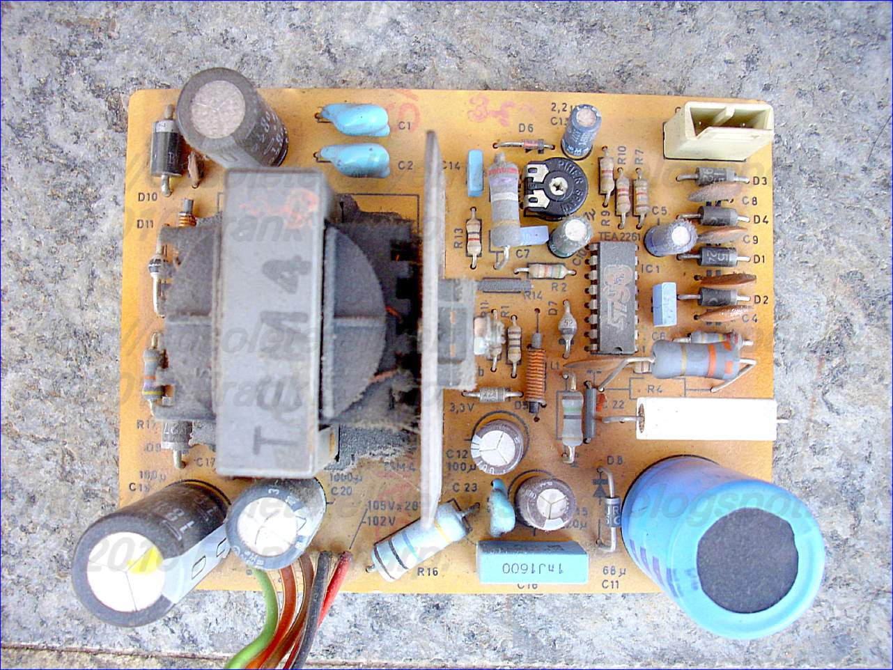
it receives pulses from the secondary. The softstarting
has to be located in the secondary regulator.
Due to the principle of the primary regulation,
pulses generated by the starting system automatically
disappear when the voltage deliv

ered by the
SMPS increases.
Stand-by Mode - Normal Mode Transition
During the transition there are simultaneously
pulses coming from the primary and secondary
regulators.
These signals are not synchronizedand some care
has to betaken toensure the safety of theswitching
power transistor.
Avery sure and simple way consist in checking the
transformer demagnetization state.
- A primary pulse is taken in account only if the
transformer is demagnetized after a conduction
of the power transistor required by the secondary
regulator.
- A secondary pulse is taken in account only if the
transformer is demagnetized after a conduction
of the power transistor required by the primary
regulator.
With this arrangement the switching safety area of
the power transistor is respected and there is no
risk of transformer magnetization.
The magnetization state of the transformer is
checked by sensing the voltage across a winding
of the transformer (generally the same which supplies
the TEA2261). This is made by connecting a
resistor between this winding and the demagnetization
sensing input of the circuit (Pin 1).
SECURITY FUNCTIONS OF THE TEA2260 (see flow-chart below)
- Undervoltage detection. This protection worksin association with the starting device ”VCC
switch” (see paragraph Starting-mode - standby
mode). If VCC is lower than VCCstop (typically
7.4V) output pulses are inhibited, in order to avoid
wrong operation of the power supply or bad
power transistor drive.
- Overvoltage detection. If VCC exceedsVCCmax
(typically 15.7V) output pulses are inhibited. Restarting
of the power supply is obtained by reducing
VCC below VCCstop.
- Current limitation of the power transistor. The
current is measured by a shunt resistor. Adouble
threshold system is used :
- When the first threshold (VIM1) is reached, the
conduction of the power transistor is stopped
until the end of the period : a new conduction
signal is needed to obtain conduction again.
- Furthermore as long as the first threshold is
reached (it means during several periods), an
external capacitor C2 is charged. When the
voltage across the capacitor reaches VC2 (typically
2.55V) the output is inhibited.This is called
the ”repetitive overload protection”. If the overload
diseappears before VC2 is reached, C2 is
discharged, so transient overloads are tolerated.
- Second current limitation threshold (VIM2).
When this thresholdis reached the output of the
circuit is immediatly inhibited. This protection is
helpfull in case of hard overload for example to
avoid the magnetization of the transformer.
- Restart of the power supply. After stopping due
to VC2, VIM2, VCCMax or VCCstop triggering, restart
of the power supply can be obtained by the
normal operating of the ”VCC switch” but thanks
to an integrted counter, if normal restart cannot
be obtained after three trials, the circuit is definitively
stopped. In this case it is necessary to
reduce VCC below approximately 5V to reset the
circuit. From a practical point of view, it means
that the power supply has to be temporarily disconnected
from any power source to get the
restart.
Synchronization + FRAME deflection output in one chip with TDA8215B (THOMSON)
Line + EHT Transformer

FEATURES SUMMARY

■ DIRECT LINE DARLINGTON DRIVE
■ DIRECT FRAME-YOKE DRIVE (± 1A)
■ COMPOSITE VIDEO SIGNAL INPUT
CAPABILITY
■ FRAME OUTPUT PROTECTION AGAINST
SHORT CIRCUITS
■ PLL
■ VIDEO IDENTIFICATION CIRCUIT
■ SUPER SANDCASTLE OUTPUT
■ VERY FEW EXTERNAL COMPONENTS
■ VERY LOWCOST POWER PACKAGE
DESCRIPTION
The TDA8215B is an horizontal and vertical deflection
circuit with super sandcastle generator
and video identification output. Used with
TDA8213 (Video & Sound IF system) and
TDA8217 (Pal decoder and video processor), this
IC permits a complete low-cost solution for PAL
applications. The TDA8215B has been specially
designed for direct drive of line DARLINGTON
transistors.

GENERAL DESCRIPTION
The TDA8215B performs all the video and power
functions required to provide signals for the line
driver and frame yoke.
It contains:
– A synchronization separator
– An integrated frame separator without external
components
– A saw-tooth generator for the frame
– A power amplifier for direct drive of frame yoke
(short circuit protected)
– An open collector output for the line darlington
drive
– A line phase detector and a voltage control
oscillator
– A super sandcastle generator
– Video identification output.
The slice level of sync-separation is fixed by value
of the external resistors R1 and R2. VR is an internally
fixed voltage.
The sync-pulse allows the discharge of the capacitor
by a 2 x I current. A line sync-pulse is not able
to discharge the capacitor under VZ/2. A frame
sync-pulse permits the complete discharge of the
capacitor, so during the frame sync-pulse Q3 and
Q4 provide current for the other parts of the circuit.
- Video chrominance and Luminance with TDA3562A,
PHILIPS TDA3562A (Philips)PAL/NTSC ONE-CHIP DECODER,
 GENERAL DESCRIPTION
The TDA3562A is a monolithic integrated decoder for the PAL and/or NTSC colour television standards. It combines all functions required for the identification and demodulation of PAL/NTSC signals. Furthermore it contains a ftuminance amplifier, an RGB-matrix and amplifier. These amplifiers supply output signals up to 4 V peak-to-peak (picture information) enabling direct drive of the discrete output stages. The circuit also contains separate inputs for data insertion, analogue as well as digital, which can be used for text display systerns (e.g. Teletext/broadcast Antiope), channel number display, etc.
Features
@ A black-current stabilizer which controls the black-currents of the three electron-guns to a level low enough to omit the black-level adjustrnent
@ Contrast control of inserted RGB signals
@ No black-level disturbance when non-synchronized external RGB signals are available on the inputs
® NTSC capability with hue control
FUNCTIONAL DESCRIPTION
Luminance amplifier The lurninance amplifier is voltage driven and requires an input signal of 450 mV peak-to-peak (positive video).
The luminance delay line must be connected between the i.f. amplifier and the decoder. The input signal is a.c. coupled to the input (pin 8). After amplification, the black level at the output of the preamplifier is clamped to a fixed d.c. level by the black level clarnping circuit. During three line periods after vertical blanking, the luminance signal is blanked out and the black tevel reference voitage is inserted by a switching circuit. This black level reference voltage is controlled via pin 11 (brightness). At the same tirne the RGB signals are clamped. Noise and residual signals have no influence during clamping thus simple internal clamping circuitry is used. Chrominance amplifiers The chrominance amplifier has ari asymmetrical input.
The input signa! must be a.c. coupled (pin 4) and have a minimum amplitude of 40 mV peak-to-peak. The gain control stage has a control range in excess of 30 dB, the maximum input signal must not exceed 1,1 V peak-to-peak, otherwise clipping of the input signal will occur. From the gain control stage the chrominance signal is fed to the saturation control stage. Saturation is linear controlled via pin 5. The control voltage range is 2 to 4 V, the input impedance is high and the saturation control range is in excess of 50 dB. The burst signal is not affected by saturation control. The signal is then fed to a gated amplifier which has a 12 dB higher gain during the chrominance signal. As a result the signal at the output (pin 28) has a burst to chrominance ratio which is 6 dB lower than that of the input signal when the saturation control is set at —6 dB. The chrominance output signal is fed tc the delay line and, after matrixing, is applied to the demodulator input pins (pins 22 and 23). These signals are fed to the burst phase detector. Oscillator and identification circuit
The burst phase detector is gatecl with the narrow part of the sandcastle pulse (pin 7). In the detector the (R-Y) and (B-Y) signals are added to provide the composite burst signal again. This composite signal is compared with the oscillator signal divided-by-2 (R-Y) reference signal. The control voltage is available at pins 24 and 25, and is also applied to the 8,8 MHz oscillator. The 4,4 MHz signal is obtained via the divide-by-2 circuit, which generates both the (B-Y) and (R-Y} reference signals and provides a 90° phase shift between them. The flip-flop is driven by pulses obtained from the sandcastle detector. For the identification of the phase at PAL mode, the (R-Y) reference signal coming from the PAL switch, is compared to the vertical signal (R-Y) of the PAL delay line. This is carried out in the H/2 detector, which is gated during burst.
When the phase is incorrect, the flip-flop gets a reset from the identification circuit. When the phase is correct, the output voltage of the H/2 detector is directly related to the burst amplitude so that this voltage can be used for the a.c.c. To avoid ‘blooming-up’ of the picture under weak input signal conditions the a.c.c. voltage is generated by peak detection of the H/2 detector output signal. The killer and identification circuits get their information from a gated output signal of the H/2 detector. Killing is obtained via the saturation control stage and the demodulators to obtain good suppression. The time constant of the saturation contro! (pin 5) provides a delayed switch-on after killing. Adjustrnent of the oscillator is achieved by variation of the burst phase detector load resistance between pins 24 and 25 (see Fig. 7). With this application the trimmer capacitor in series with the 8,8 MHz crystal (pin 26) can be replaced by a fixed value capacitor to compensate for unbalance of the phase detector.
Demodulator The (R-Y) and (B-Y) demodulators are driven by the colour difference signals from the delay-line matrix circuit and the reference signals from the 8,8 MHz divider circuit. The (R-Y) reference signal is fed via the PAL-switch.
The output signals are fed to the R and B matrix circuits and to the (G-Y) matrix to provide the (G-Y) signal which is applied to the G-matrix. The demodulation circuits are killed and blanked by by-passing the input signals. NTSC mode The NTSC mode is switched on when the voltage at the burst phase detector outputs (pins 24 and 25) is adjusted below 9 V. To ensure reliable application the phase detector load resistors are external. When the TDA3562A is used only for PAL these two 33 kQ resistors must be connected to +12 V (see Fig. 7). For PAL/NTSC application the value of each resistor must be recluced to 10 k& and connected to the slider of a potentiometer (see Fig. 8). The switching transistor brings the voltage at pins 24 and 25 below 9 V which switches the circuit to the NTSC mode.
The position of the PAL flip- flop ensures that the correct phase of the (R-Y) reference signal is supplied to the (R-Y) dernodulator. The drive to the H/2 detector is now provided by the (B-Y) reference signal. In the PAL. mode it is driven by the (R-Y) reference signal. Hue control is realized by changing the phase of the reference drive to the burst phase cletector. This is achieved by varying the voltage at pins 24 and 25 between 7,5 and 8,5 V, nominal position 8,0 V. The hue control characteristic is shown in Fig. 5. RGB matrix and amplifiers The three matrix and amplifier circuits are identical and only one circuit will be described.
The luminance and the colour difference signals are added in the matrix circuit to obtain the colour signal, which is then fed to the contrast control stage. The contrast control voltage is supplied to pin 6 (high-input impedance). The control range is +5 dB to —15 dB nominal. The relationship between the control voltage and the gain is linear (see Fig. 2). During the 3-line period after blanking a pulse is inserted at the output of the contrast control stage. The amplitude of this pulse is varied by a control voltage at pin 11. This applies a variable offset to the normai black level, thus provicling brightness control.
The brightness control range is 1 V to 3 V. While this offset level is present, the ‘black-current’ input impedance (pin 18) is high and the internal clamp circuit is activated. The clamp circuit then compares the reference voltage at pin 19 with the voltage developed across the external resistor network RA and Rp (pin 18) which is provided by picture tube beam current. The output of the comparator is stored in capacitors connected from pins 10, 20 and 21 to ground which controls the black level at the output. The reference voltage is composed by the resistor divider network and the leakage current of the picture tube into this bleeder. During vertical blanking, this voltage is stored in the capacitor connected to pin 19, which ensures that the leakage current of the CRT does not influence the black current measurement. The FGB output signals can never exceed a level of 10 V. When the signal tends to exceed this level the output signal is clipped. The black level at the outputs (pins 13, 15 and 17) will be about 3 V.
This tevel depends on the spread of the guns of the picture tube. If a beam current stabilizer is not used it is possible to stabilize the biack levels at the outputs, which in this application must be connected to the black current measuring input (pin 18} via a resistor network.
Data insertion
Each colour amplifier has a separate input for data insertion. A 1 V peak-to-peak input signal provides
a4 V peak-to-peak output signal. To avoid the ‘black-level’ of the inserted signal differing from the
black level of the normal video signal, the data is clamped to the black level of the luminance signal.
Therefore a.c. coupling is required for the data inputs.
To avoid a disturbance of the blanking level due to the clamping circuit, the source impedance of the driver circuit must not exceed 150 22.
The data insertion circuit is activated by the data blanking input (pin 9). When the voltage at this pin
exceeds a level of 0,9 V, the RGB matrix circuits are switched off and the data amplifiers are switched
on. To avoid coloured edges, the clata blanking switching time is short.
The amplitude of the data output signals is controlled by the contrast control at pin 6. The black level
is equal to the video black level and can be varied between 2 and 4 V (nominal condition) by the brightness control voltage at pin 11.
Non-synchronized data signals do not disturb the black level of the internal signals.
Blanking of RGB and data signals
Both the RGB and data signals can be blanked via the sandcastle input (pin 7). A slicing level of 1,5 V
is used for this blanking function, so that the wide part of the sandcastle pulse is separated from the
remainder of the pulse. During blanking a level of + 1 V is available at the output.
 QUICK REFERENCE DATA
Supply voltage (pin 1) Vp V1.27 typ. 12 V
Supply current (pin 1) lp = II typ. 840 mA
Luminance amplifier (pin 8)
Input voltage (peak-to—peal< value) V3,;;g7(p_p) typ. 450 mV
Contrast control range typ. 20 dB
Chrominance amplifier (pin 4)
Input voltage range (peak~to—peak value) V4_:,g7(p_p) 40 to 1100 mV
Saturation control range min. 50 dB
RGB matrix and amplifiers.
FUNCTIONAL DESCRIPTION
Luminance amplifier
The lumilnance amplifier is voltage driven and requires an input signal of 450 mV peak—to—peak (positive
video). The luminance delay line must: be connected between the i.f. amplifier and the decoder. The input
signal is a.c. coupled to the input (pin 8). After amplification, the black level at the output of the
preamplifier is clamped to a fixed (l.c. level by the black level clamping circuit.
During three line periods aifter vertical blanking, the luminance signal is blanked out and the black level
reference voltage is inserted by a switching circuit. This black level reference voltage is controlled via
pin 11 (brightness). At the same time the RGB signals are clamped. Noise and residual signals have no
influence during clamping thus; simplle internal clamping circuitry is used.
Chrominance amplifiers
The chrominance amplifier has an asymmetrical input. The input signal must be a.c. coupled (pin 4) and
have a minimum amplitude of 40 mv peak-to—pealk. The gain control stage has a control range in
excess of 30 dB, the maximum input signal must not exceed 1,1 V peak to-peak, otherwise clipping of
the input signal will occur. From the gain control stage the chromiinance signal is fed to the saturation
control stage. Saturation is linear controlled via pin 5. The control voltage range is 2 to 4 V, the input
impedance is high and the saturation control range is in excess of 50 dB. The burst signal is not affected
by saturation control. The signal is then fed to a gated amplifier which has a 12 dB higher gain during
the chrominance signal. As a result the signal at the output (pin 28) has a burst to chrominance ratiowhich is 6 dB lower than that of the input signall when the saturation control is set at -6 dB. The
chrominance output signal is fed to the delay line and, after matrixing, is applied to the demodulator
input pins (pins 22 and 23). These ‘signals are fed to the burst phase detector.
Oscillator and identification circuit
The burst phase detector is gated with the narrow part of the sandcastle pulse (pin 7). In the detector
the (Fl-Y) and (B-Y) signals are added to provide the composite burst signal again. This composite signal
is compared with the oscillator signal divided by 2 (R-Y) reference signal. The control voltage is
available at pins 24 and 25, and is also applied to the 8,8 MHZ oscillator. The 4,4 MHz signal is obtained
via the divide—by—2 circuit, which generates both the (B~Y) and (R-Y) reference signals and provides a
900 phase shift between them.
The f|ip—'flop is driven by pulses obtained from the sandcastle detector. For the identification of the
phase at PAL mode, the (Fl—Y) reference signal coming from the PAL switch, is compared to the
vertical signal (R-Y) of the PAL delay line. This is carried out in the H/2 detector, which is gated during
burst. VI/lhen the phase is incorrect, the flip-flop gets a reset from the identification circuit. When the
phase is correct, the output voltage of the H/2 detector is directly related to the burst amplitude so
that this voltage can be used for the a.c.c. To avoid ‘b|ooming~up' of the picture under weak input
signal conditions the a.c.c. voltage is generated by peak detection of the l-l/2 detector output signal.
The killer and identification circuits get their information from a gated output signal of the H/2
detector. Killing is obtained via the saturation control stage and the demodulators to obtain good
suppression. The time constant of the saturation control (pin 5) provides .3 delayed switch-on after
killing.
Adjustment of the oscillator is achieved by variation of the burst phase detector load resistance
between pins 24 and 25 (see Fig. 7). With this application the trimmer capacitor in series with the8,8 ll/IHz crystal (pin 26) can be replaced by a fixed value capacitor to compensate for unbalance of
the phase detector.
Demodulator
The (R—Y) and (B-Y) demodulators are driven by the colour difference signals from the de|ay—|ine
matrix circuit and the reference signals from the 8,8 MHZ divider circuit. The (R—Y) reference signal
is fed via the PAL—switc:h. The output signals are fed to the R and B matrix circuits and to the (G—Y)
matrix to provide the (G-Y) signal which is applied to the G«matrix. The demodulation circuits are
killed and blanked by bypassing the input signals.
NTSC: mode
The NTSC mode is switched on when the voltage at the burst phase detector outputs (pins 24 and 25)
is adjusted below 9 V. To ensure reliable application the phase detector load resistors are external.
When the TDA3562A is used only for PAL these two 33 kfl resistors must be connected to + 12 V
(see Fig. 7). For PAL/NTSC application the value of each resistor must be reduced to 10 k9: and
connected to the slider of a potentiometer (see Fig. 8). The switching transistor brings t:he voltage atpins 224 and 25 below 9 V which switches the circuit to the NTSC mode. The position of the PAL flip-
flop ensures that the correct phase of the (R—YIi reference signal is supplied to the (R-Y) demodulator.
The drive to the H/2 detector is now provided by the (B-Y) reference signal. ln the PAL mode it is
driven by the (R—Y) reference signal.
Hue control is realized by changing the phase of the reference drive to the burst phase detector. This is
achieved by varying the voltage at pins 24 and 125 between 7,5 and 8,5 V, nominal position 8,0 V. The
hue control characteristic is shown in Fig. 5.
RGB matrix and amplifiers
The three matrix and amplifier circuits are identical and only one circuit will be described.
The liuminance and the colour difference signals are added in the matrix circuit to obtain the colour
signal, which is then fed to the contrast control stage. The contrast control voltage is supplied to pin 6
(high-‘input impedance). The control range is +35 dB to ~15 dEi nominal. The relationship between the
control voltage and the gain is linear (see Fig. 2).
During the 3—line period after blanking a pulse is inserted at the output of the contrast control stage.
The amplitude of this pulse is varied by a control voltage at pin 11. This applies a variable offset to the
normal black level, thus; providing brightness control. The brightness control range is 1 V to 3 V.
While this offset level is present, the ‘black—current’ input impedance (pin 18) is high and the internal
clamp circuit is activated. The clamp circuit then compares the reference voltage at pin 19 with the
voltage developed across the exterrial resistor network RA and RB (pin 18) which is provided by
picture tube beam current. The output of the comparator is stored in capacitors connected from pins
10, IZII) and 21 to ground which controls the black level at the output. The reference voltage is composed
by the resistor divider network and the leakage current of the picture tube into this bleeder. During
vertical blanking, this voltage is stored in the capacitor connected to pin 19, which ensures that the
leakage current of the CRT does not influence the black current measurement.
The RGB output signals can never exceed a level of 10 V. When the signal tends to exceed this level
the output signal is clipped. The black level at the outputs (pins 13, 15 and 17) will be about 3 V.
This level depends on the spread of the guns of the picture tube. If a beam current stabilizer is not
used it is possible to stabilize the black levels at the outputs, which in this application must be
connected to the black current measuring input (pin 18) via a resistor network.
Data insertionEach colour amplifier has a separate input for data insertion. A 1 V peak—to—peak input signal provides
a 4 V peak—to—peak output signal. To avoid the ‘b|ack—leve|’ of the inserted signal differing from the
black level of the normal video signal, the data is clamped to the black level of the luminance signal.
Therefore a.c. coupling is required for the data inputs. To avoid a disturbance of the blanking level due
to the clamping circuit, the source impedance of the driver circuit must not exceed 150 S1).
The data insertion circuit is activated by the data blanking input (pin 9). When the voltage at this pin
exceeds a level of 0,9 V, the RGB matrix circuits are switched off and the data amplifiers are switched
on. To avoid coloured edges, the data blanking switching time is short.
The amplitude of the data output signals is controlled by the contrast control at pin 6. The black level
is equal to the video black level and can be varied between 2 and 4 V (nominal condition) by the bright-
ness control voltage at pin 11.
Non synchronized data signals do not disturb the black level of the internal signals.
Blanking of RGB and data signals
Both the RGB and data signals can be blanked via the sandcastle input (pin 7). A slicing level of 1,5 V
is used‘ for this blanking fiunction, so that the wide part of the sandcastle pulse is separated from the
rerriaindler of the pulse. During blanking a level of +1 V is available at the output.
THE PHILIPS TDA3562A Circuit arrangement for the control of a picture tube :1. Circuit arrangement for the control of at least one beam current in a picture tube by a picture comprising
a control loop which in one sampling interval obtains a measuring signal from the value of the beam current on the occurrence of a given reference level in the picture signal, stores a control signal derived therefrom until the next sampling interval and thereby adjusts the beam current to a value preset by a reference signal.
and a trigger circuit which suppresses auxiliary pulses used to generate the beam current after the picture tube has been started up and issues a switching signal for the purpose of closing the control loop during the sampling intervals and for releasing the control of the beam current by the picture signal after the measuring signal has exceeded the threshold value,
a change detection arrangement which delivers a change signal when the stored signal has assumed a largely constant value, and
a logic network which does not release the control of the beam current by the picture signal outside the sampling intervals until the change signal has also been issued after the switching signal.
2. Circuit arrangement as set forth in claim 1, in which the picture signal comprises several color signals for the control of a corresponding number of beam currents for the display of a color picture in the picture tube and the control loop stores a part measuring signal or a part control signal derived therefrom for each color signal, characterized in that the change detection arrangement includes a change detector for each color signal which delivers a part change signal when the relevant stored signal has assumed a largely constant value, and the logic network does not release the control of the beam currents by the color signals outside the sampling intervals until the part change signals have been delivered by all change detectors.
3. Circuit arrangement as set forth in claim 1, including a comparator arrangement which compares the measuring signal with the reference signal and derives the control signal from t
his
comparison, characterized in that the change detection arrangement
detects a change in the control signal with respect to time and issues
the change signal when the control signal has assumed a largely constant
value. 4. Circuit arrangement as set forth in claims 1, 2, 3 including a control signal memory which contains at least one capacitor, characterized in that the change detection arrangement delivers the change signal when a charge-reversing current of the capacitor occuring during the starting up of the picture tube falls below a limit value.
5. Circuit arrangement as set forth in claim 2, including a comparator arrangement which compares the measuring signal with the reference signal and derives the control signal from this comparison, characterized in that the change detection arrangement detects a change in the control signal with respect to time and issues the change signal when the control signal has assumed a largely constant value.
Description:
BACKGROUND OF THE INVENTIONThe invention relates to a circuit arrangement for the control of at least one beam current in a picture tube by a picture signal with a control loop which in one sampling interval obtains a measuring signal from the value of the beam current on the occurrence of a given reference level in the picture signal, stores a control signal derived therefrom until the next sampling interval and by this means adjusts the beam current to a value preset by a reference signal, and with a trigger circuit which suppresses auxiliary pulses used to generate the beam current after the picture tube is turned on and issues a switching signal for the purpose of closing the control loop during the sampling intervals and releasing the control of the beam current by the picture signal after the measuring signal has exceeded a threshold value.
Such a circuit arrangement has been described in Valvo Technische Information 820705 with regard to the integrated color decoder circuit PHILIPS TDA3562A and is used in this as a so-called cut-off point control. In the known circuit arrangement, such a cut-off point control provides automatic compensation of the so-called cut-off point of the picture tube, i.e. it regulates the beam current in the picture tube in such a way that for a given reference level in the picture signal the beam current has a constant value despite tolerances and changes with time (aging, thermal modifications) in the picture tube and the circuit arrangement, thereby ensuring correct picture reproduction.
Such a blocking point control is particularly advantageous for the operation of a picture tube for the display of color pictures because in this case there are several beam currents for different color components of the color picture which have to be in a fixed ratio with one another. If this ratio changes, for example, as the result of manufacturing tolerances or ageing processes, distortions of the colors occur in the reproduction of the color picture. The beam currents, therefore, have to be very accurately balanced. The said cut-off point control prevents expensive adjustment and maintenance time which is otherwise necessary.
Conventional picutre tubes are constructed as cathode-ray tubes with hot cathodes which require a certain time after being turned on for the hot cathodes to heat up. Not until a final operating temperature has been reached do these hot cathodes emit the desired beam currents to the full extent, while gradually rising beam currents occur in the time interval when the hot cathodes are heating up. The instantaneous values of these beam currents depend on the instantaneous temperatures of the hot cathodes and on the accelerating voltages for the picture tube which build up simultaneously with the heating process and are undefined until the end of the heating time. After the picture tube is turned on, these values initially produce a highly distorted picture until the beam currents have attained their final value. These picture distortions after the picture tube is turned on are even further intensified by the fact that the cut-off point control is not yet adjusted to the beam currents which flow after the heating time is over.
For the purpose of suppressing distorted pictures during the heating time of the hot cathodes, the known circuit arrangement has a turn-on delay element operating as a trigger circuit which, in essence, contains a bistable flip-flop. When the picture tube and the circuit arrangement controlling the beam currents flowing in it are turned on, the flip-flop is switched into a first state in which it interrupts the supply of the picture signal to the picture tube. Thus, during the heating time the beam currents are suppressed, and the picture tube does not yet display any picture. In sampling intervals which are provided subsequent to flybacks of the cathode beam into an initial position on the changeover from the display of one picture to the display of a subsequent picture and even within the changeover, that is outside the display of pictures, the picture tube is controlled for a short time in such a way that beam currents occur when the hot cathodes are sufficiently heated up and an accelerating voltage is resent. If these currents exceed a certain threshold value, the flip-flop circuit switches into a second state and releases the picture signal for the control of the beam currents and the cut-off point control.
It is found, however, that the picture displayed in the picture tube immediately after the switching over of the flip-flop is still not fault-free. Because, in fact, the beam currents are supported during the heating time of the hot cathodes, the cut-off point control cannot respond yet. This response of the cut-off point control takes place only after the beam currents are switched on, i.e. after the flip-flop is switched into the second state and therefore at a time in which the picture signal already controls the beam currents. In this way the response of the blocking point control makes its presence felt in the picture displayed.
With the known circuit arrangement the brightness of the picture gradually increases, during the response of the cut-off point control, from black to the final value.
This slow increase in the picture brightness after the tube is turned on is disturbing to the eyes of the viewer not only in the case of the black-and-white picture tubes with one hot cathode, but especially so in the case of colour picture tubes which usually have three hot cathodes. With a color pi
cture tube, color purity errors can
also occur in addition to the change in the picture brightness if, as a
result of different speeds of response of the cut-off point control for
the three beam currents, there are found to be intermittent variations
from the interrelation between the beam currents required for a correct
picture reproduction.SUMMARY OF THE INVENTION
The aim of the invention is to create a circuit arrangement which suppresses the above-described disturbances of brightness and color of the displayed picture when the picture tube is being started.
The invention achieves this aim in that a circuit arrangement of the type mentioned in the preamble contains a change detection arrangement which emits a change signal when the stored signal has assumed an essentially constant value, and a logic network which does not release the control of the beam current by the picture signal until the change signal has also been emitted after the switching signal.
In the circuit arrangement according to the invention, therefore, the display of the picture is suppressed after the picture tube is turned on until the cut-off point control has responded. If the picture signal then starts to control the beam current, a perfect picture is displayed immediately. In this way, all the disturbances of the picture which affect the viewer's pleasure are suppressed. The circuit arrangement of the invention is of simple design and can be combined on one semiconductor wafer with the existing picture signal processing circuits and also, for example, with the known circuit arrangement for cut-off point control. Such an integrated circuit arrangement not only requires very little space on the semiconductor wafer, but also needs no additional external leads. Thus the circuit arrangement of the invention can be arranged, for example, in an integrated circuit which has precisely the same external connections as known integrated circuits. This means that an integrated circuit containing the circuit arrangement of the invention can be directly incorporated in existing equipment without the need for additional measures.
In one embodiment of the said circuit arrangement, in which the picture signal contains several color signals for the control of a corresponding number of beam currents for representing a color picture in the picture tube and, for each color signal, the control loop stores a part measuring signal or a part control signal derived from it, the change detection arrangement contains a change detector for each color signal which emits a part change signal when the relevant stored signal has assumed an essentially constant value, and the logic network does not release the control of the beam currents by the color signals outside the sampling intervals until the part change signals have been emitted from all change detectors.
In principle, therefore, such a circuit arrangement has three cut-off point controls for the three beam currents controlled by the individual color signals. To reduce the cost of the circuitry, the measuring stage is common to all the cut-off point controls, as in the known circuit arrangement. All three beam currents are then measured successively by this measuring stage. In this way, a part measuring signal or a part control signal derived from it is obtained for each beam current and is stored sespar
ately according to which of the beam
currents it belongs. Changes in the part measuring signal or part
control signal are detected for each beam current by one of the change
detectors each time. Each of these change detectors issues a part change
signal to the logic network. The latter does not release the control of
the beam currents by the picture signal outside the sampling intervals
until all the part change signals indicate that the part measuring
signal or the part control signal, as the case may be, remains constant.
This ensures that the cut-off point controls for the beam currents of
all color signals have responded when the picture appears in the picture
tube. In a further embodiment of the circuit arrangement according to the invention with a comparator arrangement which compares the measuring signal with the reference signal and derives the control signal from this comparison, the change detection arrangement detects a change in the control signal with respect to time and issues the change signal when the control signal has assumed an essentially constant value. In the case of the representation of a color signal the comparator arrangement derives several part control signals, whose changes with time are detected by the change detectors, from a corresponding comparison of the part measuring signals with the reference signal. In this embodiment of the circuit arrangement of the invention, preference is given to storage of only the control signal or the part control signals for the purpose of controlling the beam currents.
In another embodiment of the circuit arrangement of the invention which includes a control signal memory which contains at least one capacitor in which a charge or voltage corresponding to the control signal is stored, the change detection arrangement issues the change signal when a charge-reversing current of the capacitor occurring during the turning on of the picture tube has fallen below a limit value and has thus at least largely decayed. Such a detection of the steady state of the cut-off point control is independent of the actual magnitude of the control signal and therefore independent of, for example, the level of the picture tube cut-off voltage, circuit tolerances or ageing processes in the circuit arrangement or the picture tube.
Detection of whether or not the charge-reversing current exceeds the limit value is performed preferentially by a current detector which is designed with a current mirror system which is arranged in a supply line to a capacitor acting as a control signal store. A current mirror arrangement of this kind supplies a current which coincides very precisely with the charging current of the capacitor. This current is then compared, preferably in a further device contained in the change detection arrangement, with a current representing a limit value or, after conversion into a voltage, with a voltage representing the limit value. The change signal is obtained from the result of this comparison.
On the other hand, digital memories may also be used as control signal memories, especially when the picture signal is supplied as a digital signal and the blocking point control is constructed as a digital control loop. In such a case, the comparator arrangement, the change detection arrangement and the trigger circuit are also designed as digital circuits. Then, the change detection arrangement advantageously forms the difference of the signals stored in the control signal memory in two successive sampling intervals and compares this with the limit value formed by a digital value. If the difference falls short of the limit value, the change signal is issued.
BRIEF DESCRIPTION OF THE DRAWINGS
An embodiment of the invention is described in greater detail below with the aid of the drawings in which:
FIG. 1 shows a block circuit diagram of the embodiment,
FIG. 2 shows a somewhat more detailed block circuit diagram of the embodiment,
FIG. 3 shows time-dependency diagrams of some signals occurring in the circuit diagram shown in FIG. 2, and
FIG. 4 shows a somewhat moredetailed block circuit diagram of a part of the circuit diagram shown in FIG. 2.
 DETAILED DESCRIPTION OF THE INVENTION
FIG. 1 shows a block circuit diagram of a circuit arrangement to which a picture signal is fed via a first input 1 of a combinatorial stage 2. From the output 3 of the combinatorial stage 2 the picture signal is fed to the picture signal input of a controllable amplifier 5 which at an output 6 issues a current controlled by the picture signal. This current is fed via a measuring stage 7 to a hot cathode 8 in a picture tube 9 and forms therein a beam current of a cathode ray by means of which a picture defined by the picture signal is displayed on a fluorescent screen of the picture tube 9.
The measuring stage 7 measures the current fed to the hot cathode 8, i.e. the the beam current in the picture tube 9, and at a measuring signal output 10, issues a measuring signal corresponding to the magnitude of this current. This is fed to a measuring signal input 11 of a comparator arrangement 12 to which a reference signal is supplied at a reference signal input 13. In a preferably periodically recurring sampling interval during the occurrence of a given reference level in the picture signal, the comparator arrangement 12 forms a control signal from the value of the measuring signal fed to the measuring signal input 11 at this time, on the one hand, and the reference signal, on the other, by means of substraction and delivers this at a control signal output 14. From there the control signal is fed to an input 15 of a control signal memory 16 and is stored in the latter. The control signal is fed via an output 17 of the control signal memory 16 to a second input 18 of combinatorial stage 2 in which it is combined with the picture signal, e.g. added to it.
The combinatorial stage 2, the controllable amplifier 5, the measuring stage 7, the comparator arrangement 12 and the control signal memory 16 form a control loop with which the beam current is guided towards the reference signal in the sampling interval during the occurrence of the reference level in the picture signal. For the reference level, use is made in particular of a black level or a level with small, fixed distance from the black level, i.e. a value in the picture signal which produces a black or almost back picture area in the displayed picture in the picture tube. In this case the control loop, as described, forms a cut-off point control for the picture tube. If the reference level is away from the black level, the control loop is also designated as quasi-cut-off-point control.
The circuit arrangement as shown in FIG. 1 also has a trigger circuit 19 to which the measuring signal from the measuring signal output 10 of measuring stage 7 is fed at a measuring signal input 20. When the circuit arrangement and therefore the picture tube are turned on, the trigger circuit 19 is set in a first state in which by means of a first connection 21 it blocks the comparator arrangement 12 in such a way that the latter delivers no control signal or a control signal with the value zero at its control signal output 14. This prevents the control signal memory 16 from storing undefined values for the control signal at the moment of turning on or immediately thereafter.
The circuit arrangement shown in FIG. 1 also has a logic network 22 which is connected via a second connection 23, by means of which a switching signal is supplied, with the trigger circuit 10 and via a third connection 24 with the controllable amplifier 5. Like the trigger circuit 19, the logic network 22 also finds itself controlled, when the circuit arrangement is being turned on, by the switching signal in a first stage in which by way of the third connection 24 it blocks the controllable amplifier 5 with a blocking signal in such a way that no beam currents controlled by the picture signal can yet flow in the picture tube 9. Thus the picture tube 9 is blanked; no picture is displayed yet.
When picture tube 9 is turned on, the hot cathode 8 is still cold so that no beam current can flow anyhow. The hot cathode 8 is then heated up and, after a certain time, begins gradually to emit electrons as the result of which a cathode ray and therefore a beam current can form. However, during the heating up of the hot cathode 8, and because the cut-off point control has not yet responded, this would be undefined and is therefore suppressed by the controllable amplifier 5. Only in time intervals which are provided immediately subsequent to flybacks of the cathode rays into an initial position at the changeover from the display of one image to that of a subsequent image, but even before the start of the display of the subsequent image, the controllable amplifier 5 delivers a voltage in the form of an auxiliary pulse for a short time at its output 6, and when the hot cathode 8 in the picture tube 9 is heated up sufficiently, this voltage produces a beam current. The time interval for the delivery of this voltage is selected in such a way that a cathode ray produced by its does not produce a visible image in the picture tube 9, and coincides for example with the sampling interval.
The measuring stage 7 measures the short-time cathode current produced in the manner described and, at its measuring signal output 10, delivers a corresponding measuring signal which is passed via measuring signal output 20 to the trigger circuit 19. If the measuring signal exceeds a definite preset threshold value, the trigger circuit 19 is switched into a second state in which it releases t
he comparator arrangement 12 via the first connection 12 and,
by means of the second connection 23, uses the switching signal to also
bring the logic network 22 into a second state. The comparator
arrangement 12 now evaluates the measuring signal supplied to it via the
measuring signal input 11, i.e. it forms the control signal as the
difference between the measuring signal and the reference signal
supplied via the reference signal input 13. The control signal is
transferred via the control signal output 14 and the input 15 into the
control signal memory 16. It is subsequently fed via the output 17 of
the control signal memory 16 to the second input 18 of the combinatorial
stage 2 and is there combined with the picture signal at the first
input 1, e.g. is superimposed on it by addition. This superimposed
picture signal is fed to the picture signal input 4 of the controllable
amplifier 5 via the output 3 of the combinatorial stage 2. In the second state of the logic network 22 the controllable amplifier 5 is switched via the third connection 24 by the blocking signal in such a way that the picture signal controls the beam currents only during the sampling intervals and that, for the rest, no image appears yet in the picture tube. The cut-off point control now gebins to respond, i.e. the value of the control signal is changed by the control loop comprising the combinatorial stage 2, the controllable amplifier 5, the measuring stage 7, the comparator arrangement 12 and the control signal memory 16 until such time as the beam current in the picture tube 9 at the blocking point or at a fixed level with respect to it is adjusted to a value preset by the reference signal. For this purpose the sampling interval, in which the picture signal controls the beam current via the controllable amplifier 5 is selected in such a way that within it the picture signal just assumes a value corresponding to the cut-off point or to a fixed level with respect to it.
During the response of the cut-off point control the control signal fed to the control signal memory 16 changes continuously. Between the control signal output 14 of the comparator arrangement 12 and the input 15 of the control signal memory 16 is inserted a changed detection arrangement 25 which detects the variations of the control signal. When the cut-off point control has responded, i.e. the control signal has assumed a constant value, the change detection arrangement 25 delivers a change signal at an output 26 which indicates that the steady stage of the cut-off point control is achieved and the said signal is fed to a change signal input 27 of the logic network 22. The logic network then switches into a third state in which via the third connection 24 it enables the controllable amplifier 5 in such a way that the beam currents are now controlled without restriction by the picture signal. Thus a correctly represented picture appears in the picture tube 9.
A shadow-like representation of individual constituents of the circuit arrangement in FIG. 1 is used to indicate a modification by which this circuit arrangement is equipped for the representation of color pictures in the picture tube 9. For example, three color signals are fed in this case as the picture signal via the input 1 to the combinatorial stage 2. Accordingly, the input 1 is shown in triplicate, and the combinatorial stage 2 has a logic element, e.g. an adder, for example of these color signals. The controllable amplifier 5 now has three amplifier stages, one for each of the color signals, and the picture tube now contains three hot cathodes 8 instead of one so that three independent cathode rays are available for the three color signals.
However, to simplify the circuit
arrangement and to save on components, only one measuring stage 7 is
provided which measures all three beam currents successively. Also, the
comparator arrangement 12 forms part control signals from the
successively arriving part measuring signals for the individual beam
currents with the reference signal, and these part control signals are
allocated to the individual color signals and passed on to three storage
units which are contained in the control signal memory 16. From there,
the part control signals are sent via the second input 18 of the
combinatorial stage 2 to the assigned logic elements. The circuit arrangement thus forms three independently acting control loops for the cut-off point control of the individual color signals, in which case only the measuring stage 7 and to some extent at least the comparator arrangement 12 are common to these control loops.
The change detection arrangement 25 now has three change detectors each of which detects the changes with time of the part control signals relating to a color signal. Then via the output 26 each of these change detectors delivers a part change signal to the change signal input 27 of the logic network 22. These part change signals occur independently of one another when the relevent control loop has responded. The logic network 22 evaluates all three part change signals and does not switch into its third stage until all part change signals indicate a steady state of the control loops. Only then, in fact, is it ensured that all the color signals from the beam currents controlled by them are correctly reproduced in the picture tube, and thus no distortions of the displayed image, especially no color purity errors, occur. The color picture displayed then immediately has the correct brightness and color on its appearance when the picture tube is turned on.

FIG. 2 shows a somewhat more detailed block circuit diagram of an embodiment of a circuit arrangement equipped for the processing of a picture signal containing three colour signals. Three color signals for the representation of the colors red, green and blue are fed to this circuit arrangement via three input terminals 101, 102, 103. A red color signal is fed via the first input terminal 101 to a first adder 201, a green colour signal is fed via the second input terminal to a second adder 202, and a blue colour signal is fed via the third input terminal 103 to a third adder 203. From outputs 301, 302 and 303 of the adders 201, 202, 203 the color signals are fed to amplifier stages 501, 502 and 503 respectively. Each of the amplifier stages contains a switchable amplifier 511, 512 and 513, an output amplifier 521, 522 and 523 as well as a measuring transistor 531, 532 and 533 respectively. The emitters of these measuring transistors 531, 532, 533 are each connected to a hot cathode 801, 802, 803 of the picture tube 9 and deliver the cathode currents, whereas the collectors of measuring transistors 521, 532, 533 are connected to one another and to a first te
rminal 701 of a measuring
resistor 702 the second terminal of which 703 is connected to earth. The
current gain of the measuring transistors 531, 532 and 533 is so great
that their collector currents coincide almost with the cathode currents.
By measuring the voltage drop produced by the cathode currents at the
measuring resistor 802 it is then possible to measure the cathode
currents and therefore the beam currents in the picture tube 9 with
great accuracy. The falling voltage at the measuring resistor 702 is fed as a measuring signal to an input 121 of a buffer amplifier 120 with a gain factor of one, at the output 122 of which the unchanged measuring signal is therefore available at low impedance. From there it is fed to a first terminal 131 of a reference voltage source 130 which is connected with its second terminal 132 to inverting inputs 111, 112 and 113 of three differential amplifiers 123, 124, 125 respectively. The differential amplifiers 123, 124, 125 also each have a non-inverting input 114, 115, and 116 respectively. These are connected to each other at a junction 117, to earth via a leakage current storage capacitor 126 and to the output 122 of the buffer amplifier 120 via decoupling resistor 118 and a leakage current sampling switch 119. In addition, the input 121 of the buffer amplifier 120 can be connected to earth via a short-circuiting switch 127.

The operation of the comparator arrangement 12 which consists mainly of the buffer amplifier 120, the reference voltage source 130 and differential amplifiers 123, 124, 125 will be explained below with the aid of the pulse diagrams in FIG. 3. FIG. 3a shows a horizontal blanking signal for a television signal which, as the picture signal, controls the beam currents in the picture tube 9. In this diagram, H represents horizontal blanking pulses which follow one another in the picture signal at the time interval of one line duration and by means of which the beam currents are switched off during line flyback between the display of the individual picture lines in the picture tube. FIG. 3b shows a vertical blanking pulse V by means of which the beam currents are switched off during the change ober from the display of one picture to the display of the next picture. FIG. 3c shows a measuring signal control pulse VH which is formed from a vertical blanking pulse lengthened by three line duration.
The short-circuiting switch 127 is now controlled in such a way that it is non-conducting only throughout the duration of the measuring signal control pulse VH and during the remaining time short-circuits the input 121 of the buffer amplifier 120 to earth. This means that a measuring signal only reaches the comparator arrangement 12 during frame change so that the parts of the picture signal which control the beam currents producing the picture in the picture tube exert no influence on comparator arrangement 12 and therefore on the blocking point control.
Throughout the duration of the measuring signal control pulse VH, the measuring signal from output 122, reduced by a reference voltage issued by the reference voltage source 130 between its first 131 and its second terminal 132, is present at the inverting inputs 111, 112, 113 of differential amplifiers 123, 124, 125. If the differential amplifiers 123, 124, 125 were not present, this difference would be fed directly as part control signals to the control signal storage capacitors 161, 162, 162. The differential amplifiers 123, 124, 125 amplify the difference and thus form the control amplifiers of the control loops.
The comparator arrangement 12 further contains a device for compensation of the influence of any leakage currents occurring in the picture tube 9. For this purpose, a voltage to which the leakage current storage capacitor 126 is charged is fed to the non-inverting inputs 114, 115, 116 of the three differential amplifiers 123, 124 and 125. The charging is performed by the measuring signal from output 122 of the buffer amplifier 120 via the decoupling resistor 118 and the leakage current sampling switch 119 which is closed only within the period of the vertical blanking pulse V, and in certain cases only during part of the latter. Within this time the beam currents are, in fact, totally switched off by the picture signal so that in certain cases only a leakage current flows through the measuring resistor 702. Consequently, throughout the duration of the vertical blanking pulse V the measuring signal co
rresponds to this leakage current. Because the leakage current
also flows during the remaining time, even outside the duration of the
vertical blanking pulse the measuring signal contains a component
originating from the leakage current which therefore is also contained
in the voltage fed to the inverting inputs 111, 112, 113 of differential
amplifiers 123, 124, 125 and is subtracted out in the differential
amplifiers 123, 124, 125. The part control signal is fed from output 141 of differential amplifier 123 by the first control signal sampling switch 154 to the first terminal 151 of the first control signal storage capacitor 161 during the period of a storage pulse L1 and is stored in the said capacitor. Similarly, the part control signal from output 143 of differential amplifier 125 is fed to the third control signal storage capacitor 163 during the period of a storage pulse L2 and the part control signal from output 142 of differential amplifier 124 is fed to the second control signal storage capacitor 162 during a storage pulse L3. The storage pulses L1, L2 and L3 are illustrated in FIGS. 3d, e and f. They lie in sequence in one of the three line periods by which the measuring signal control pulse VH is longer than the vertical blan
king pulse V. These three line periods form
the sampling interval for the measuring signal or the part measuring
signals, as the case may be. During the remaining periods the outputs,
141, 152, 143 of the differential amplifiers 123, 124, 125 are isolated
from the control signal storage capacitors 161, 162, 163 so that no
interference can be transmitted from there and any distortion of the
stored part control signals caused thereby is eliminated. For the
duration of storage pulses L1, L2 and L3 the color signals at the input
terminals 101, 102, 103 are at their reference level i.e. in the present
embodiment at a level, corresponding to the blocking point or at a
fixed level with respect to it so that the control loops can adjust to
this level.The switchable amplifiers 511, 512, and 513 each receive at each input 241, 242, 243 a blanking signal BL1, BL2, BL3 respectively, the curves of which are shown in FIGS. 3g, h, i. These blanking signals interrupt the supply of the color signals during line flybacks and frame change, i.e. during the period of the measuring signal control pulse VH, and thus the beam currents in these time intervals are switched off. Naturally, the red color signal is let through during the first line period after the end of the vertical blanking pulse V, the blue color signal during the second line period after the end of the vertical blanking pulse V and the green color signal during the third line period after the end of the vertical blanking pulse V by the switchable amplifiers 511, 512, 513 respectively so that they can control the beam currents. Blanking signals BL1, BL2 and BL3 also provide for interruptions in the frame change blanking pulse, which corresponds to the measuring signal control pulse, in the corresponding time intervals. In these time intervals the beam currents are measured and part control signals are determined from the part measuring signals and stored in the control signal storage capacitors 161, 162, 163.
The circuit arrangement shown in FIG. 2 further contains a trigger circuit 19 to which a supply voltage is fed via a supply terminal 190. Via a reset input 191 a voltage is also
supplied to
the trigger circuit 19 from a third terminal 133 of the reference
voltage source 130. When the circuit arrangement is turned on, this
voltage is designed so as to be delayed with respect to the supply
voltage so that when the circuit arrangement is brought into operation
the interplay of the two voltages produces a switch-on reset signal such
that a low-value voltage pulse occurs at the reset input 191 during
turn on, which means that the trigger circuit 19 is set in its first
state. The reset input 191 can also be connected to another circuit of
any configuration which generates a switch-on reset signal when the
picture tube is turned on. The trigger circuit 19 is further connected via a second connection 23 to a logic network 22 which, when the circuit arrangement is turned on, is also set into a first state via the second connection 23. In this first state the logic network 22 delivers a blocking signal at a blocking output 240 which is fed to the three switchable amplifiers 511, 512, 513. By this means the supply of the color signals to the output amplifiers 521, 522, 523 is interrupted completely so that no beam currents can be generated by these. No picture is therefore displayed.
An insertion signal EL which extends over the three line periods by which the measuring signal control pulse VH is longer than the vertical blanking pulse V, i.e. over the sampling interval, is also fed via a line 233 to the trigger circuit 19 and the logic network 22. As long as the trigger circuit 19 is in its first state, this insertion pulse EL is issued via a control output 192 from the trigger circuit 19 and fed to the pulse generator 244. During the period of the insertion pulse EL this generator produces a voltage pulse of a definite magnitude and passes this to output amplfiiers 521, 522, 523 as an auxiliary pulse via switching diodes 245, 246, 247. By this means the beam currents are switched on for a short time so as to receive a measuring signal despite the disconnected color signals as soon as at least one of the hot cathodes 801, 802, 803 delivers a beam current.
In its first state the trigger circuit 19 also delivers a signal via a control line 211, and this signal is used to switch the outputs 141, 142, 143 of the differential amplifiers 123, 124, 125 to earth potential or practically to earth potential. This suppresses effects of voltages at the inputs 111 to 116 of the differential amplifiers 123, 124, 125, especially effects of the reference voltage source 130 which may in some cases initiate incorrect charging of the control signal storage capacitors 161, 162, 163.
The measuring signal produced by means of the pulse generator 244 at the input 121 of the buffer amplifier 120 is also fed to the trigger circuit 19 via a measuring signal input 20. If it exceeds a preset threshold value, the trigger circuit 19 switched into its second state. The logic network 22 is then also switched into its second state via the second connection 23. The differential amplifiers 123, 124, 125, too, are triggered by the signal along the control line 211 into issuing a control signal defined by the difference in the voltages at its inputs 111 to 116. The pulse generator 244 is blocked by the control output 192. The blocking signal issued from the blocking output 240 of the logic network 22 now turns on the switchable amplifiers 511, 512, 513 in the time intervals defined by the storage pulses L1, L2, L3 in such a way that in these time intervals the color signals can produce beam currents to form a measuring signal by which the control loops respond. However, the display of the picture is still suppressed. The control signal storage capacitors 161, 162, 163 are charged up in this process. In the leads to the first terminals 151, 152, 153 there are change detectors 251, 252, 253 which detect the changes of the charging currents of the control signal storage capacitors 161, 162, 163 and at their outputs 261, 262, 263 in each case deliver a part change signal when the charging current of the control signal storage capacitor in question has decayed and thus the relevant control loop has responded. The part change signals are fed to three terminals 271, 272, 273 of the change signal input 27 of the logic network 22.
When part change signals are present from all change detectors 251, 252, 253, when therefore all control loops have responded, the logic network 22 switches from its second to its third state. The blocking signal from the blocking output 240 is now completely disconnected such that the switchable amplifiers 511, 512, 513 are now switched only by the blanking signals BL1, BL2, BL3. The colour signals are then switched through to the output amplifiers 521, 522, 523 and the picture is displayed in the picture tube.

FIG. 4 shows an embodiment for a trigger circuit 19 and a logic network 22 of the circuit arrangements as shown in FIGS. 1 or 2. The trigger circuit 19 contains a flip-flop circuit formed from two NAND-gates 194, 195 to which the switch-on reset signal, by which the trigger circuit 19 is returned to its first stage, is fed via the reset input 191. All the elements of the circuit arrangement in FIG. 4 are shown in positive logic. Thus, a short-time low voltage at the reset input 191 immediately after the circuit arrangement is started up is used to set the flip-flop circuit 194, 195 in such a way that a high voltage occurs at the output of the second NAND gate 194 and a low voltage at the output of the second NAND gate 195. The low voltage at the output of the second NAND gate 195 blocks differential amplifiers 123, 124, 125 via the control line 211 in the manner described.
The insertion pulse EL is fed via the line 233 to the trigger circuit 19, is combined via an AND gate 196 with the signal from the output of the first NAND gate 194 and is delivered at the control output 192 for the purpose of controlling the pulse generator 244.
The signals from the outputs of the NAND-gates 194, 195 are fed via a first line 231 and a second line 232 of the second connection 23 as a switching signal to the logic network 22. The first line 231 is connected to reset inputs R of three part change signal memories 221, 222, 223 in the form of bistable flip-flop circuits which when the circuit arrangement is started up are reset via the first line 231 in such a way that they carry a low voltage at their outputs Q. The second line 232 of the second connection 23 leads via three AND gates 224, 225, 226 to setting inputs S of the three part change signal memories 221, 222, 223. By means of the AND gates 224, 225, 226 the signal on the second line 232 of the second connection 23 is combined each time with one of the part change signals supplied via the terminals 271, 272, 273. The signals from the outputs Q of the part change signal memories 221, 222, 223 are combined by means of a collecting gate 227 in the form of an NAND gate and a
re held ready at
its output 228. The measuring signal is fed to the trigger circuit 19 via the measuring signal input 20 and passed to a first input 197 of a threshold detector 198 to which at a second input a threshold value, in the form of a threshold voltage for example, produced by a threshold generator 199 is also supplied. When the voltage at the first input 197 of the threshold detector 198 is smaller than the voltage delivered by the threshold generator 199, the threshold detector 198 delivers a high voltage at its output 200. When, on the other hand, the voltage at the first input 197 is greater than the voltage of the threshold generator 199, the voltage at the output 200 jumps to a low value. This voltage is supplied as the setting signal of the flip-flop circuit 194, 195, reverses the latter and thereby switches the trigger circuit 19 into its second state when the voltage at the first input 197 exceeds the voltage of the threshold generator 199.
Between the output 200 and the flip-flop circuit 194, 195 in the circuit arrangem
ent
shown in FIG. 4 there is inserted an inquiry gate 181 in the form of an
OR gate to which an inquiry pulse is fed via an inquiry input 193 of
the trigger circuit 19. This ensures that the flip-flop circuit 194, 195
is switched over only at a time fixed by the inquiry pulse--in the
present case a negative voltage pulse--and not at any other times due to
disturbances. As such an inquiry pulse it is possible to use, for
example, a pulse which occurs in the second line period after the end of
the vertical blanking pulse V, i.e. one which largely corresponds to
the storage pulse L2. After the switching over of the flip-flop circuit 194, 195 corresponding to the setting of the trigger circuit 19 into the second state, appropriately modified signals are supplied via the control line 211 and the output 192 for the purpose of controlling the pulse generator 244 and the differential amplifiers 123, 124, 125. Modified voltages also appear on the lines 231, 232 of the second connection 23, and these voltages release the part change signal memories 221, 222, 223 such that they can each be set when the part change signals reach the terminals 271, 272, 273.
In certain cases, a further flip-flop circuit 234 is inserted in the lines 231, 232 to delay the signals passing along these lines; this is reset via the first line 231 when the circuit arrangement is started up and thus it also resets the part change signal memories 221, 222, 223. However, after the trigger circuit 19 is switched into the second state the further flip-flop circuit 234 is not set via the second line 232 of the second connection 23 until a release pulse arrives via a release input 235 and another AND gate 236, for example a period of approximately the interval of two vertical blanking pulses V after the switching of the trigger circuit 19 into the second state. In this way it is possible to bridge a period of time in which no defined signal values are present at the terminals 271, 272, 273.
The signal at the output 228 of the collecting gate 227 changes its state when the last of the three part change signals has also arrived and has set the last of the three part change signal memories. The signal is then combined via a gate arrangement 229 of two NAND gates and one AND gate with the insertion pulse EL of line 223 and with the signal on the second line 232 of the second connection 23 or from the output Q of the further flip-flop circuit 234 to the blocking signal delivered at the blocking output 24 which is fed to the switchable amplifiers 511, 512, 513.
The circuit arrangement described is designed in such a way that the trigger circuit 19 remains in its second state and logic network 22 remains in its third state even if charging currents reappear at the difference signal storage cpacitors 161, 162, 163 due to disturbances during the operation of the circuit arrangement. The cutoff point control then makes readjustments without the displayed picture being disturbed.
In the circuit arrangement shown in F
IG. 2, the green
color signal can also be let through during the second line period after
the end of the vertical blanking pulse V and the blue color signal
during the third line period after the end of the vertical blanking
pulse V by the switchable amplifiers 511, 512, 513 for the purpose of
controlling the beam currents. The storage pulses L2 and L3 at the
control signal sampling switches 155 and 156 and the second and third
blanking signals BL2 and BL3 at the blanking inputs 242 and 243 are then
to be interchanged. The resulting insertion signals A2 and A3 as shown
in FIGS. 3m and n are also interchanged then accordingly. In FIG. 2 a dashed line is used to indicate which components of the circuit arrangement can be combined advantageously to form an integrated circuit. The first terminals 151, 152, 153 of the difference signal storage capacitors 161, 162, 163, one terminal 128 of leakage current storage capacitor 126, three terminals 524, 525, 526 in the leads to the output amplifiers 521, 522, 523 as well as a line connection 704 between the first terminal 701 of the measuring resistor 702 and the input 121 of the buffer amplifier 120 will then form the connecting contacts of this integrated circuit
-----------------------------------------------------


Tuner and Frequency synthesizer + prescaler and Video IF and Sound 1 IF In One module.
Frequency synthesizer + prescaler with SDA3302 (SIEMENS)
Video IF with TDA8341 (PHILIPS)
Mixer + osc with TDA5330T (PHILIPS)
TDA5330T VHF, UHF and Hyperband mixer/oscillator for TV and VCR 3-band tuners
GENERAL DESCRIPTIONThe TDA5330T is a monolithic integrated circuit that performs the band A, band B and band C mixer/oscillator functions
in TV and VCR tuners. This device gives the designer the capability to design an economical and physically small 3-band
tuner which will be capable of meeting the most stringent requirements e.g. FTZ or FCC. The tuner development time
can be drastically reduced by using this device.
Features
· Balanced mixer with a common emitter input for band A
· Amplitude-controlled oscillator for band A
· Balanced mixer with common base input for band B and C
· Balanced oscillator for band B and C
· Local oscillator buffer output for external prescaler
· SAW filter preamplifier with an output impedance of 100 W
· Bandgap voltage stabilizer for oscillator stability
· Electronic bandswitch
------------------------------------------------------------
TSA5511 1.3 GHz Bidirectional I2C-bus
FEATURES
· Complete 1.3 GHz single chip system
· Low power 5 V, 35 mA
· I2C-bus programming
· In-lock flag
· Varicap drive disable
· Low radiation
· Address selection for Picture-In-Picture (PIP), DBS
tuner (3 addresses)
· Analog-to-digital converter
· 8 bus controlled ports (5 for TSA5511T), 4 current
limited outputs (1 for TSA5511T), 4 open collector
outputs (bi-directional)
· Power-down flag
APPLICATIONS
· TV tuners
· VCR Tuners
GENERAL DESCRIPTION
The TSA5511 is a single chip PLL frequency synthesizer
designed for TV tuning systems. Control data is entered
via the I2C-bus; five serial bytes are required to address
the device, select the oscillator frequency, programme the
eight output ports and set the charge-pump current. Four
of these ports can also be used as input ports (three
general purpose I/O ports, one ADC). Digital informationconcerning those ports can be read out of the TSA5511 on
the SDA line (one status byte) during a READ operation.
A flag is set when the loop is “in-lock” and is read during a
READ operation. The device has one fixed I2C-bus
address and 3 programmable addresses, programmed by
applying a specific voltage on Port 3. The phase
comparator operates at 7.8125 kHz when a 4 MHz crystal
is used.
controlled synthesizer
------------------------------------
PHILIPS TDA8341 Television IF amplifier and demodulator
DESCRIPTION
The TDA8340;Q and TDA8341;Q are integrated IF
amplifier and demodulator circuits for colour or black/white
television receivers, the TDA8340;Q is for application with
n-p-n tuners and the TDA8341;Q for p-n-p tuners.
The TDA8340;Q and TDA8341;Q are pin-compatible
successors with improved performance to types
TDA2540/2541;Q and TDA3540/3541;Q.
Features
· Full range gain-controlled wide-band IF amplifier
· Linear synchronous demodulator with excellent
intermodulation performance
· White spot inverter
· Wide-band video amplifier with noise protection
· AFC circuit with AFC on/off switching and
sample-and-hold function
· Low impedance AFC output
· AGC circuit with noise gating
· Tuner AGC output for n-p-n tuners (TDA8340) or p-n-p
tuners (TDA8341)
· External video switch for switching-off the video output
· Reduced sensitivity for high sound carriers
· Integrated filter to limit
second harmonic IF signals· Wide supply voltage range
· Requires few external components.
- Audio IC TDA8190.
DESCRIPTION
The TDA8190is a completeTV soundchannel with
DC tone and volume controls plus separate VCR
input and output connections. Mounted in a Powerdip
16 + 2 + 2 package, the device delivers an
output power of 4W into 16W (d = 10%, Vs = 24V)
or 1.5W into 8W (d = 10%, Vs = 12V). Included in
the TDA8190 are : IF amplifier limiter, active lowpass
filter, AF pre-amplifier and power amplifier,
turn-off muting, mute circuit and thermal protection.
High output, high sensitivity, excellentAM rejection
and low distortion make the device suitable for use
in TVs of almost every type. Further, no screening
is necessary because the device is free of radiation
problems.
SDA2516 EAROM
Features- Word-organized reprogrammable nonvolatile memory
in n-channel floating-gate technology (E2PROM)
- 128 ´ 8-bit organization
- Supply voltage 5 V
- Serial 2-line bus for data input and output (I2C Bus)
- Reprogramming mode, 10 ms erase/write cycle
- Reprogramming by means of on-chip control (without
external control)
- Check for end of programming process
- Data retention > 10 years
- More than 104 reprogramming cycles per address
- Compatible with SDA 2516. Exception:
Conditions for total erase and current consumption.
I2C Bus Interface
The I2C Bus is a bidirectional 2-line bus for the transfer of data between various integrated circuits.
It consists of a serial data line SDA and a serial clock line SCL. The data line requires an external
pull-up resistor to VCC (open drain output stage).
The possible operational states of the I2C Bus are shown in figure 1. In the quiescent state, both
lines SDA and SCL are high, i.e. the output stage of the data line is disabled. As long a SCL remains
"1", information changes on the data bus indicate the start or the end of data transfer between two
components.
The transition on SDA from "1" to "0" is a start condition, the transition from "0" to "1" a stopcondition. During a data transfer the information on the data bus will only change while the clock line
SCL is "0". The information on SDA is valid as long as SCL is "1".
In conjunction with an I2C Bus system, the memory component can operate as a receiver and as a
transmitter (slave receiver or slave transmitter). Between a start and stop condition, information is
always transmitted in byte-organized form. Between the trailing edge of the eighth clock pulse and a ninth acknowledge clock pulse, the memory component sets the SDA line to low as a confirmation
of reception, if the chip select conditions have been met. During the output of data, the data output
of the memory is high in impedance during the ninth clock pulse (acknowledge master).
The signal timing required for the operation of the I2C Bus is summarized in figure 2.
Control Functions of the I2C Bus
The memory component is controlled by the controller (master) via the I2C Bus in two operating
modes: read-out cycle, and reprogramming cycle, including erase and write to a memory address.
In both operating modes, the controller, as transmitter, has to provide 3 bytes and an additional
acknowledge clock pulse to the bus after the start condition. During a memory read, at least nine
additional clock pulses are required to accept the data from the memory and the acknowledge
master, before the stop condition may follow. In the case of programming, the active programming
process is only started by the stop condition after data input (see figure 3).
The chip select word contains the 3 chip select bits CS0, CS1 and CS2, thus allowing 8 memory
chips to be connected in parallel. Chip select is achieved when the three control bits logically
correspond to the selected conditions at the select inputs.
Check for End of Programming or Abortion of Programming Process
If the chip is addressed during active reprogramming by entering CS/E, the programming process
is terminated. If, however, it is addressed by entering CS/A, the entry will be ignored. Only after
programming has been terminated will the chip respond to CS/A. This allows the user to check
whether the end of the programming process has been reached (see figure 3).
Memory Read
After the input of the first two control words CS/E and WA, the resetting of the start condition and the
input of a third control word CS/A, the memory is set ready to read. During acknowledge clock
nine, the memory information is transferred in parallel mode to the shift register. Subsequent to the
trailing edge of the acknowledge clock, the data output is low impedance and the first data bit can
be sampled, (see figure 4).
With every shift clock, an additional bit reaches the output. After reading a byte, the internal address
counter is automatically incremented when the master receiver switches the data line to “low” during
the ninth clock (acknowledge master). Any number of memory locations can thus be read one after
the other. At address 128, an overflow to address 0 is not initiated. With the stop condition, the data
output returns to high-impedance mode. The internal sequence control of the memory component
is reset from the read to the quiescent with the stop condition.
Memory Reprogramming MIVAR CM2 UNITThe reprogramming cycle of a memory word comprises an erase and a subsequent write process.
During erase, all eight bits of the selected word are set into "1" state. During write, "0" states are
generated according to the information in the internal data register, i.e. according to the third input
control word.
After the 27th and the last clock of the control word input, the active programming process is started
by the stop condition. The active reprogramming process is executed under onchip control.
The time required for reprogramming depends on component deviation and data patterns.
Therefore, with rated supply voltage, the erase/write process extends over max. 20 ms, or more
typically, 10 ms. In the case of data word input without write request (write request is defined as data
bit in data register set to “0”), the write process is suppressed and the programming time is
shortened. During a subsequent programming of an already erased memory address, the erase
process is suppressed again, so that the reprogramming time is also shortened.
ST6306B1/KC MIVAR ST63PXX 8-BIT HCMOS PIGGYBACK MCUS. FOR TV APPLICATIONS
DEVICE TYP
E :_ ST63 PO6/ 7/8
- ST63P1 6/7/8
_ ST63P26/7/8
_ ST63P36/7/8
_ ST63 P56/7/8
EMULATION OF ST63XX DIP MASKED DEVICES
PIN TO PIN REPLACEMENT OF ALL ROM
MASKED DEVICES
8-BIT ARCHITECTURE
STATIC HCMOS OPERATION
4.5 T0 5.5 V SUPPLY OPERATING RANGE
4MHZ CLOCK OPERATION
PROGRAM ROM 2 16K BYTES EXTERNAL
DATA ROM 2 USER SELECTABLE SIZE
DATA RAM : 256 BYTES
DATA EEPROM : 128 BYTES
40/42 SHRINK/48 PIN DUAL—|N—L|NE PIGGY-
BACK CERAMIC PACKAGE
14/15 BIT PHASE LOCKED LOOP PERIPHE-
RAL (PLL, ST63P16/7/8, ST63P36/7/8 ONLY)
14 BIT VOLTAGE SYNTHESIS TUNING PE-
RIPHERAL (VS, ST63P56/7/8 only)
SAME I/O PORT CONFIGURATION AS IN THE
MASKED PRODUCTS, INCLUDING DIRECT
LED DRIVING OUTPUTS
TWO TIMERS EACH INCLUDING AN 8-BIT
COUNTER WITH A 7—B|T PROGRAMMABLE
PRESCALER
DIGITAL WATCHDOG
May 1989
ADVANCE DATA
SERIAL PERIPHERAL INTERFACE (SPI) SUP-
PORTING S—BUS IZCBUS AND STANDARD
SERIAL PROTOCOLS
ON—CHIP 5 LINES BY 15 COLUMNS ON-
SCREEN-DISPLAY GENERATOR (NOT
AVAILABLE ON ST63P06/07/08 AND
ST63P1 6/7/8)
FOUR 6-BIT PWM D/A CONVERTERS
I AFC A/D CONVERTER WITH 0.5V RESOLU-
TION
INFRARED SIGNAL PRE—PROC ESSOR
- THREE INTERRUPT VECTORS(|R,TIMER 1 &
2, ST63PO6/7/8, ST63P16/7/8)
FOUR INTERRUPT VECTORS (IR, TIMER 1 &
2, OSD VSYNC, ST63P26/7/8, ST63P36/7/8,
ST63P56/7/8)
ON-CHIP CLOCK OSCILLATOR
ON-BOARD POWER—ON RESET CIRCUITRY
BYTE EFFICIENT INSTRUCTION SET
BIT TEST AND JUMP INSTRUCTIONS
WAIT AND BIT MANIPULATION INSTRUC-
TIONS
3_25ps TCYCLE (WITH 4.0 MHz CLOCK)
I TRUE LIFO 6—LEVEL STACK
THE DEVELOPMENT TOOL OF THE ST63XX
MICFIOCONTROLLERS CONSISTS OF THE
EMST63 HW/TVS EMULATION AND DEVEL-
OPMENT SYSTEM AND CONNECTED VIA A
STANDARD RS232 SERIAL LINE TO AN MSDOS PC.
GENERAL DESCRIPTION
The ST63PXX microcontrollers are piggyback
members of the 8-bit HCMOS ST63XX family, a
series of devices specially oriented to TV applica-
tions. Different packages and configurations are
available to offer different performance/cost trade-
offs. All ST63XX members are based on a building
block approach: to a common Core is associated a
combination of on-chip peripherals (macrocells)
available from a standard |ibrary.These peripherals
are designed with the same Core technology giving
full compatibility, short design and testing time.
Many of these macrocells are specially dedicated to
TV applications. These piggyback devices have the
same functions and pin configuration as all ROM
ST63XX masked products. In the piggyback de-
vices instead of on-chip program and data ROM, the
relevant "address" and "data" lines are lead out to
the 28 pin socket which is directly located on the top
of the package, so that an external memory can be
addressed. These piggyback devices can operate
as an emulator to verify the user code, or for proto-
type/small volume production in order to test design
concept before commitment is made to high volume
production with masked ST63XX devices. The mac-
rocells of the ST63PXX are: two 8-bit counter with
a 7-bit programmable prescaler (Timer), a Digital
Watchdog Timer, a Serial Peripheral Interface (SPI),
a 5 lines by 15 columns On-screen display gener-
ator (OSD, not available on ST63P06/7/8,
ST63P16/7/8), four 6-Bit PWM D/A Converters, an
AFC A/D converter with 0.5V resolution, a 14 bit
Phase Locked Loop peripheral (PLL, ST63P16/7/8,
ST63P36/7/8 only). a 14 bit Voltage synthesis tun-
ing peripheral (VS, ST63P56/7/8 only). In addition
all these devices have 128 bytes of on-chip EE-
PROM. Refers to ST63XX masked devices data-
sheets for additional information.
No comments:
Post a Comment
The most important thing to remember about the Comment Rules is this:
The determination of whether any comment is in compliance is at the sole discretion of this blog’s owner.
Comments on this blog may be blocked or deleted at any time.
Fair people are getting fair reply. Spam and useless crap and filthy comments / scrapers / observations goes all directly to My Private HELL without even appearing in public !!!
The fact that a comment is permitted in no way constitutes an endorsement of any view expressed, fact alleged, or link provided in that comment by the administrator of this site.
This means that there may be a delay between the submission and the eventual appearance of your comment.
Requiring blog comments to obey well-defined rules does not infringe on the free speech of commenters.
Resisting the tide of post-modernity may be difficult, but I will attempt it anyway.
Your choice.........Live or DIE.
That indeed is where your liberty lies.
Note: Only a member of this blog may post a comment.