


TBA920 line oscillator combination
 DESCRIPTION
The line oscillator combination TBA920 is a monolithic
integrated circuit intended for the horizontal deflection of the black and white
and colour TV sets
picture tube.
FEATURES:
SYNC-PULSE SEPARATION
OPTIONAL NOISE INVERSION
GENERATION OF A LINE FREQUENCY VOL-
TAGE BY MEANS OF AN OSCILLATOR
PHASE COMPARISON BETWEEN SYNC-
PULSE AND THE OSCILLATOR WAVEFORM
PHASE COMPARISON BETWEEN THE OS-
CILLATOR WAVEFORM AND THE MIDDLE OF
THE LINE FLY-BACK PULSE
AUTOMATIC SWITCHING OF THE VARIABLE
TRANSCONDUCTANCE AND THE VARIABLE
TIME CONSTANT TO ACHIEVE NOISE SUP-
PRESSION AND, BY SWITCHING OFF, POS-
SIBILITY OF TAPE-VIDEO-REGISTERED RE-
PRODUCTION
SHAPING AND AMPLIFICATION OF THE OS-
CILLATOR WAVEFORM TO OBTAIN PULSES
FOR THE CONTROL OF DRIVING STAGES IN
HORIZONTAL, DEFLECTION CIRCUITS
USING EITHER TRANSISTORS OR THYRISTORS
 Power
Supply: The examples chosen are taken from manufacturers' circuit
diagrams and are usually simplified to emphasise the fundamental nature
of the circuit. For each example the particular transistor properties
that are exploited to achieve the desired performance are made clear. As
a rough and ready classification the circuits are arranged in order of
frequency: this part is devoted to circuits used at zero frequency,
field frequency and audio frequencies. Series Regulator Circuit Portable
television receivers are designed to operate from batteries (usually
12V car batteries) and from the a.c. mains. The receiver usually has an
11V supply line, and circuitry is required to ensure that the supply
line is at this voltage whether the power source is a battery or the
mains. The supply line also needs to have good regulation, i.e. a low
output resistance, to ensure that the voltage remains constant in spite
of variations in the mean current taken by some of the stages in the
receiver. Fig. 1 shows a typical circuit of the power -supply
arrangements. The mains transformer and bridge rectifier are designed to
deliver about 16V. The battery can be assumed to give just over 12V.
Both feed the regulator circuit Trl, Tr2, Tr3, which gives an 11V output
and can be regarded as a three -stage direct -coupled amplifier. The
first stage Tr 1 is required to give an output current proportional to
the difference between two voltages, one being a constant voltage
derived from the voltage reference diode D I (which is biased via R3
from the stabilised supply). The second voltage is obtained from a
preset potential divider connected across the output of the unit, and is
therefore a sample of the output voltage. In effect therefore Tr 1
compares the output voltage of the unit with a fixed voltage and gives
an output current proportional to the difference between them. Clearly a
field-effect transistor could do this, but the low input resistance of a
bipolar transistor is no disadvantage and it can give a current output
many times that of a field-effect transistor and is generally preferred
therefore. The output current of the first stage is amplified by the two
subsequent stages and then becomes the output current of the unit.
Clearly therefore Tr2 and Tr3 should be current amplifiers and they
normally take the form of emitter followers or common emitter stages
(which have the same current gain). By adjusting the preset control we
can alter the fraction of the output voltage' applied to the first stage
and can thus set the output voltage of the unit at any desired value
within a certain range. By making assumptions about the current gain of
the transistors we can calculate the degree of regulation obtainable.
For example, suppose the gain of Tr2 and Tr3 in cascade is 1,000, and
that the current output demanded from the unit changes by 0.1A (for
example due to the disconnection of part of the load). The corresponding
change in Tr l's collector current is 0.1mA and, if the standing
collector current of Tr 1 is 1mA, then its mutual conductance is
approximately 4OmA/V and the base voltage must change by 2.5mV to bring
about the required change in collector current. If the preset potential
divider feeds one half of the output voltage to Tr l's base, then the
change in output voltage must be 5mV. Thus an 0.1A change in output
current brings about only 5mV change in output voltage: this represents
an output resistance of only 0.0552.
Power
Supply: The examples chosen are taken from manufacturers' circuit
diagrams and are usually simplified to emphasise the fundamental nature
of the circuit. For each example the particular transistor properties
that are exploited to achieve the desired performance are made clear. As
a rough and ready classification the circuits are arranged in order of
frequency: this part is devoted to circuits used at zero frequency,
field frequency and audio frequencies. Series Regulator Circuit Portable
television receivers are designed to operate from batteries (usually
12V car batteries) and from the a.c. mains. The receiver usually has an
11V supply line, and circuitry is required to ensure that the supply
line is at this voltage whether the power source is a battery or the
mains. The supply line also needs to have good regulation, i.e. a low
output resistance, to ensure that the voltage remains constant in spite
of variations in the mean current taken by some of the stages in the
receiver. Fig. 1 shows a typical circuit of the power -supply
arrangements. The mains transformer and bridge rectifier are designed to
deliver about 16V. The battery can be assumed to give just over 12V.
Both feed the regulator circuit Trl, Tr2, Tr3, which gives an 11V output
and can be regarded as a three -stage direct -coupled amplifier. The
first stage Tr 1 is required to give an output current proportional to
the difference between two voltages, one being a constant voltage
derived from the voltage reference diode D I (which is biased via R3
from the stabilised supply). The second voltage is obtained from a
preset potential divider connected across the output of the unit, and is
therefore a sample of the output voltage. In effect therefore Tr 1
compares the output voltage of the unit with a fixed voltage and gives
an output current proportional to the difference between them. Clearly a
field-effect transistor could do this, but the low input resistance of a
bipolar transistor is no disadvantage and it can give a current output
many times that of a field-effect transistor and is generally preferred
therefore. The output current of the first stage is amplified by the two
subsequent stages and then becomes the output current of the unit.
Clearly therefore Tr2 and Tr3 should be current amplifiers and they
normally take the form of emitter followers or common emitter stages
(which have the same current gain). By adjusting the preset control we
can alter the fraction of the output voltage' applied to the first stage
and can thus set the output voltage of the unit at any desired value
within a certain range. By making assumptions about the current gain of
the transistors we can calculate the degree of regulation obtainable.
For example, suppose the gain of Tr2 and Tr3 in cascade is 1,000, and
that the current output demanded from the unit changes by 0.1A (for
example due to the disconnection of part of the load). The corresponding
change in Tr l's collector current is 0.1mA and, if the standing
collector current of Tr 1 is 1mA, then its mutual conductance is
approximately 4OmA/V and the base voltage must change by 2.5mV to bring
about the required change in collector current. If the preset potential
divider feeds one half of the output voltage to Tr l's base, then the
change in output voltage must be 5mV. Thus an 0.1A change in output
current brings about only 5mV change in output voltage: this represents
an output resistance of only 0.0552.Power supply is realized with mains transformer and Linear transistorized power supply stabilizer, A DC power supply apparatus includes a rectifier circuit which rectifies an input commercial AC voltage. The rectifier output voltage is smoothed in a smoothing capacitor. Voltage stabilization is provided in the stabilizing circuits by the use of Zener diode circuits to provide biasing to control the collector-emitter paths of respective transistors.A linear regulator circuit according to an embodiment of the present invention has an input node receiving an unregulated volt
age and an output node providing a regulated voltage. The linear regulator circuit includes a voltage regulator, a bias circuit, and a current control device.In one embodiment, the current control device is implemented as an NPN bipolar junction transistor (BJT) having a collector electrode forming the input node of the linear regulator circuit, an emitter electrode coupled to the input of the voltage regulator, and a base electrode coupled to the second terminal of the bias circuit. A first capacitor may be coupled between the input and reference terminals of the voltage regulator and a second capacitor may be coupled between the output and reference terminals of the voltage regulator. The voltage regulator may be implemented as known to those skilled in the art, such as an LDO or non-LDO 3-terminal regulator or the like.
The bias circuit may include a bias device and a current source. The bias device has a first terminal coupled to the output terminal of the voltage regulator and a second terminal coupled to the control electrode of the current control device. The current source has an input coupled to the first current electrode of the current control device and an output coupled to the second terminal of the bias device. A capacitor may be coupled between the first and second terminals of the bias device.
In the bias device and current source embodiment, the bias device may be implemented as a Zener diode, one or more diodes coupled in series, at least one light emitting diode, or any other bias device which develops sufficient voltage while receiving current from the current source. The current source may be implemented with a PNP BJT having its collector electrode coupled to the second terminal of the bias device, at least one first resistor having a first end coupled to the emitter electrode of the PNP BJT and a second end, a Zener diode and a second resistor. The Zener diode has an anode coupled to the base electrode of the PNP BJT and a cathode coupled to the second end of the first resistor. The second resistor has a first end coupled to the anode of the Zener diode and a second end coupled to the reference terminal of the voltage regulator. A second Zener diode may be included having an anode coupled to the cathode of the first Zener diode and a cathode coupled to the first current electrode of the current control device.
A circuit is disclosed for improving operation of a linear regulator, having an input terminal, an output terminal, and a reference terminal. The circuit includes an input node, a transistor, a bias circuit, and first and second capacitors. The transistor has a first current electrode coupled to the input node, a second current electrode for coupling to the input terminal of the linear regulator, and a control electrode. The bias circuit has a first terminal for coupling to the output terminal of the linear regulator and a second terminal coupled to the control electrode of the transistor. The first capacitor is for coupling between the input and reference terminals of the linear regulator, and the second capacitor is for coupling between the output and reference terminals of the linear regulator. The bias circuit develops a voltage sufficient to drive the control terminal of the transistor and to operate the linear regulator. The bias circuit may be a battery, a bias device and a current source, a floating power supply, a charge pump, or any combination thereof. The transistor may be implemented as a BJT or FET or any other suitable current controlled device.

GRUNDIG EXCLUSIV 1452 IT CHASSIS 29300-277.03
Tuning unit with bandswitch for high frequency receivers
Abstract:
A
tuning unit with a bandswitch for high frequency receivers having a
potentiometer system for the control of capacity diodes is disclosed.
The potentiometer system includes a plurality of parallelly disposed
resistance paths on which wipers can be moved by means of screw tuning
spindles mounted beside one another in a common housing made of an
insulating material. The bandswitch is formed of metal wires and is
associated with each tuning spindle. The tuning spindles are joined for
rotation with sleeves simultaneously forming the operating knobs which
are carried in apertures in the front plate and each have a flange
engaging the back side of the front plate about the apertures. The
flange is slightly larger than the cross section of the apertures and
tapers conically away from the back side of the front plate.
1.
Tuning unit with bandswitch for high frequency receivers having
potentiometer means for the control of capacity diodes composed of a
plurality of parallelly disposed resistance paths on which wipers are
moved by means of screw tuning spindle means mounted beside one another
in a common housing of insulating material, bandswitch means formed of
metal wires associated with each tuning spindle means, said tuning
spindle means being joined for rotation with sleeve means simultaneously
forming operating knobs which are borne in apertures in the front
plate and each sleeve means having an axial flange surface engaging the
back side of the front plate about one aperture therein, said flange
surface being slightly larger than the cross section of the apertures
and tapering conically away from the back side of the front plate.2. Tuning unit of claim 1 wherein the sleeve means are joined telescopically and coaxially with the tuning spindle means, and the flange surface engages the back side of the front plate when the sleeve means are in the state wherein they are pulled out of the front plate.
3. Tuning unit of claim 1 wherein the ends of the tuning spindle means which are opposite the front plate have each an annular groove into which a spring bracket engages whose bent end is supported against the housing and which has two diametrically disposed spring arms having opposite spring curvature, the said spring arms in each case contacting the opposite axial walls of the groove.
4. Tuning unit of claim 3 wherein the spring bracket rests with its bent end against the housing and the spring arms additionally engage a bracket formed on the housing or an intermediate bracket formed in one piece with the connection soldering lugs.
5. Tuning unit of claim 3 wherein the spring bracket is formed in one piece with the connection soldering lugs and has spring arms curved both in the same direction which engage an axial wall of the annular groove in the spindle and the opposite axial wall rests against a housing wall.
6. Tuning unit of claim 1 wherein the pointers associated with each potentiometer means lie on the one hand in windows associated with each tuning spindle means in the front plate, and on the other hand are rotatably mounted with their ends opposite the front plate in pivot pins on the housing, and the guiding pin of the spindle nuts carried in a longitudinally displaceable manner on each tuning spindle is provided with a slit disposed parallel to the longitudinal axis of the tuning spindle and slides with its peripheral surface resiliently within the slide tract of the pointer.
7. Tuning unit of claim 1 wherein the bandswitches are formed each of a displaceable metal rod which is in working engagement with stationary metal rods common to all bandswitches of a tuning unit, contacting each of them individually.
8. Tuning unit of claim 7 wherein the metal rods are metal wires.
9. Tuning unit of claim 7 wherein the metal rods are stamped metal parts.
10. Tuning unit of claim 7 wherein levers of insulating material are placed on the front ends of the displaceable metal rods and extend through windows which are provided with detents and which are associated with each tuning spindle in the housing front plate, while the opposite ends are held fixedly in the rearward end of the housing, and the displaceable metal rods individually make contact with contact cams on the stationary metal rods, these cams being in an offset array corresponding to the detents in the windows, the corresponding rods extending parallel to the front plate and parallel to one another behind the front plate.
11. Tuning unit of claim 7 wherein insulating material bridges or insulating material slide pieces are inserted between the contact cams of two adjacent, stationary metal rods and within the free space between two such parallel metal rods.
12. Tuning unit of claim 7 wherein the displaceable metal rods have, in the vicinity of their mountings on the housing, an articulation in the form of a vertically disposed flat portion.
Description:
BACKGROUND
The invention relates to a tuning unit with bandswitch for high frequency receivers, especially radio and television receivers, having a potentiometer system for the control of capacity diodes, the said potentiometer system consisting of a plurality of parallel resistance paths along which wiper contacts can be driven by means of screw spindles disposed adjacent one another in a common insulating material housing in which a bandswitch formed of metal rods is associated with each tuning spindle.
In these tuning units, the working voltages of the capacity diodes in the tuning circuits are recorded once a precise tuning to the desired frequency has been performed. A potentiometer tuning system has great advantages over the formerly used channel selectors operating with mechanically adjustable capacitors (tuning condensers) or mechanically adjustable inductances (variometers), mainly because it is not required to have such great precision in its tuning mechanism.
Tuning units with bandswitches formed of variable resistances and combined with interlocking pushbuttons controlling the supply of recorded working voltages to capacity diodes are known. Channel selection is accomplished by depressing the knobs, and the tuning or fine tuning are performed by turning the knobs. The resistances serving as voltage dividers in these tuning units are combined into a component unit such that they are in the form of a ladderlike pattern on a common insulating plate forming the cover of the housing in which the tuning spindles and wiper contacts corresponding to the variable resistances are housed. The number of resistances corresponds to the number of channels or frequencies which are to be recorded. The wiper contact picks up a voltage which, when applied to the capacity diodes determines their capacitance and hence the frequency of the corresponding oscillating circuit. The adjustment of the wipers is performed by turning the tuning spindle coupled to the tuning knob. By the depression of a button the electrical connection between a contact rod and a tuning spindle is brought about and thus the selected voltage is applied to the capacity diodes. Since the push buttons release one another, it is possible simply by depressing another button to tune to a different receiving frequency or a different channel, as the case may be.
To permit the switching of a number of channels in a certain tuning range, bandswitches for a plurality of tuning ranges, such as UHF and VHF for example, are often provided in the tuning units described above. In the pushbutton tuning unit of the above-named type, the bandswitch consists of a printed circuit board which is fastened on the housing of the tuning unit, and a switch lever which is preset by means of the pushbutton by turning, and is operated by depressing the pushbutton while at the same time selecting the channel.
Where this combination of knobs and pushbuttons is not possible, the selection of the range is accomplished by means of an additional lever which can be set over to select the range.
 However,
since such tuning units require too many riveting operations when they
are assembled, tuning units were later created in which the individual
parts in the voltage divider and pushbutton housing were loosely
inserted and/or held in place by projections, lugs, hooks or tabs of
resilient plastic. In spite of these initial improvements, the
bandswitch, especially the one associated with the tuning units, was
still technically intricate and very expensive.
However,
since such tuning units require too many riveting operations when they
are assembled, tuning units were later created in which the individual
parts in the voltage divider and pushbutton housing were loosely
inserted and/or held in place by projections, lugs, hooks or tabs of
resilient plastic. In spite of these initial improvements, the
bandswitch, especially the one associated with the tuning units, was
still technically intricate and very expensive.
THE INVENTION
It is the object of the invention, therefore, to create an additionally improved and simplified tuning unit containing a bandswitch of simple, space-saving and reliably operating design.
In accordance with the invention, this object is accomplished in a tuning unit with bandswitch of the kind described in the beginning by joining the tuning spindles for rotation with sleeves simultaneously forming the control knobs, which are mounted in apertures in the front plate of the housing and have each a flange engaging the back of the front plate around the aperture, the said flange being slightly larger than the aperture and tapering conically away from the back of the front plate.
In further development, the sleeves can be joined telescopically for rotation with the tuning spindles, and the flange is able to engage the back side of the front plate when the sleeve is in the position in which it is drawn out of the front plate. The sleeves constructed in this manner, whose portions projecting from the apertures in the front plate form the control knobs for the tuning spindles, permit easy assembly of the tuning unit and at the same time assure positive co-rotation of sleeves and spindles. The sleeves can be pushed from the front side of the front plate through the apertures onto the clutch surfaces of the spindles, this inward pushing being easily accomplished on account of the taper, and the dropping out of the sleeve being prevented by the flange engaging the back of the front plate. If the control knobs project only slightly out of the front plate, they can be operated from the outside by inserting a tool into them. With the telescoping type of coupling, however, it is possible to draw the sleeves or control knobs further outwardly so that they can be rotated by hand without the use of tools.
To provide constant assurance of the axial fixation of the tuning spindles, the tuning spindle ends farthest from the front plate can each be provided with an annular groove engaged by a spring bracket whose one leg is supported against the housing and whose other leg is forked to form two spring arms, each bent in the opposite direction and each engaging one of the two opposite walls of the annular groove. The tuning spindles are secured against axial displacement by this construction of the invention alone, without the need for further measures. This facilitates the joining of the sleeves or control knobs to the tuning spindle, because in this case there is no need for precise axial fixation and extreme dimensional accuracy.
Furthermore, the indicators associated with each potentiometer can be mounted in windows in the front plate which are associated with each tuning spindle or tuning knob for visual indication at the front, the other extremities farthest from the front plate being mounted for pivoting on pins set in the housing; the guiding pin on the spindle nut that is driven longitudinally on each tuning spindle can be provided with a slit disposed parallel to the long axis of the tuning spindles and can slide within the indicator slide lever slot, with its surface resiliently engaging the walls of said slot.
In an especially advantageous embodiment, the tuning unit can have bandswitches each formed of a displaceable metal rod which is in contacting engagement individually with stationary metal rods which are common to all of the bandswitches of a tuning unit. It contrast to the bandswitches known hitherto, which as a rule consist of a printed circuit board with switchable contacts thereon, this frequency bandswitch of the invention is of great simplicity, can be manufactured simply and inexpensively, and at the same time is very reliable in operation.
The displaceable and stationary metal rods of the bandswitches can be formed of metal wires or they can be of stamped sheet metal. Also, in further expansion of the concept of the invention, the stationary metal rods thus formed can be all entirely alike and merely offset from one another, thereby further simplifying the manufacture and stocking thereof.
To permit connection also to audiovisual apparatus, one or more of the stationary metal rods can be divided electrically into at least two parts each.
In a special development of this concept, lugs of insulating material can be mounted on the front ends of the displaceable metal wires, these lugs extending through windows in the front plate of the housing which are associated with each tuning spindle and are provided with detents, while the opposite ends can be held fixedly at the rear end of the housing, and the displaceable metal wires can make contact with contact humps on the stationary metal wires, the humps being offset from one another to correspond to the detents in the windows, and the stationary metal wires extending in back of the front plate, parallel to the latter and parallel to one another.
To increase switching reliability, bridges or sliding pieces made of insulating material can be inserted between the contact humps of adjacent stationary wires within the free space between two such parallel lying metal wires.
To achieve easy displacement of the displaceable metal wires despite the fixed end mounting on the housing, the displaceable metal wires, in further embodiment of the invention, can have each an articulation adjacent their end mountings, in the form of a vertically disposed flattened portion. This flat permits the metal wires to be deflected horizontally against a weak spring bias.
DESCRIPTION OF THE DRAWING
As an example of the embodiment of the invention, there is represented in the drawings a tuning unit with bandswitch for television receivers. In these drawings,
FIG. 1 is a front elevational view of a tuning unit with bandswitch,
FIG. 2 is a plan view showing the bandswitch of the tuning unit of FIG. 1,
FIG. 3 is a side elevational, cross-sectional view of the tuning unit of FIG. 1,
FIG. 4 is a rear elevational view of the tuning unit of FIG. 1,
FIG. 5 is a plan view showing the indicator means of the tuning unit of FIG. 1,
FIG. 6 shows the sleeve with the operating knob and tuning spindle,
FIG. 7 shows the telescoping manner in which the sleeve is joined to the tuning spindle,
FIG. 8 is a fragmentary view of the bandswitch,
FIG. 9 is another fragmentary view of the bandswitch, and
FIG. 10 shows how the tuning spindle is fixed in position.
DESCRIPTION
The method of representation used in the drawings is greatly simplified, for the purpose of better del ineating
the features of the invention. The tuning unit with bandswitch
consists of an insulating material housing 1 with a front plate 2,
which is closed by a cover plate 3 accommodating the resistance paths.
The housing 1 is divided by parallel sidewalls 4 into chambers in which
the tuning spindles 5 are disposed.
ineating
the features of the invention. The tuning unit with bandswitch
consists of an insulating material housing 1 with a front plate 2,
which is closed by a cover plate 3 accommodating the resistance paths.
The housing 1 is divided by parallel sidewalls 4 into chambers in which
the tuning spindles 5 are disposed.
The embodiments is an 8-fold tuning unit having eight bandswitches assocated with each tuning spindle, and eight indicators.
Accordingly, there are eight apertures 6 in a central row, through which the operating knobs 7 of the sleeves 8 coupled with the tuning spindles 5 are passed. The operating knobs 7 have recessed surfaces 9 for turning with a turning tool. In a row extending parallel above the row of the apertures 6 there are eight windows 10, whose upper edge is provided with notches 11. Lugs 12 of insulating material extend through the windows 10 and engage the upper notches 11 and are joined behind the front plate to displaceable metal wires 13 of the bandswitch. In a row located beneath the row of apertures 6 another eight windows 14 are provided, through which the ends of the pointers of the indicators 15 protrude.
Now,
the bandswitch consists in each case of a displaceable metal wire 13
which can be brought into working engagement with stationary metal
wires 16, which are all of the same construction and are only disposed
offset from one another. While the displaceable metal wire 13 extends
substantially parallel to the longitudinal axis and thus at right
angles to the front plate 2, the stationary, parallelly disposed metal
wires 16 are parallel to the front plate 2 and are thus inserted at a
right angle to the displaceable metal wire. A departure from
parallelism or from the right angle, as the case may be, takes place
substantially only when the displaceable metal wire 13 is deflected to
the two outer notches. The rearward end 18 of the displaceable metal
wire, which forms a vertical loop, is tightly inserted into a receiver
17. Just ahead of the loop 18, the metal wire 13 is provided with a
vertically disposed portion 19 by a flattening on the metal wire 13.
The movement, when the metal wire 13 is deflected into the desired
notches or detents, takes place horizontally by the flex ing
of these portions 19. The stationary metal wires 16 are held tightly
in their positions in projections 20 on the housing, or by lugs or the
like. Since three switch actions are provided, that is, three ranges,
for each tuning spindle, a bandswitch consists of one displaceable metal
wire and three stationary metal wires 16, which are used for all
switches.
ing
of these portions 19. The stationary metal wires 16 are held tightly
in their positions in projections 20 on the housing, or by lugs or the
like. Since three switch actions are provided, that is, three ranges,
for each tuning spindle, a bandswitch consists of one displaceable metal
wire and three stationary metal wires 16, which are used for all
switches.
To permit each bandswitch to have exactly three switching actions, each of the three stationary metal wires 16 has one contact hump 21 corresponding to one of the detents 11 in the windows 10 of the front plate 2. The contact humps 21 are thus located one next to the other as seen from the front plate 2. So that the displaceable metal wire 13 will always come into mechanical and electrical contact only with the desired contact hump, and prevent short circuits, insulating bridges 22 are installed between the adjacent metal wires 16, said insulating bridges being stationary.
If more or less than three switching actions are desired, all that need be done in the case of the bandswitch of the invention is to change the number of stationary metal rods or wires accordingly.
The sleeves 8 with the operating knob 7 have a flange 23 engaging the back of the front plate 2 and tapering back to the point where it joins the tuning spindle. This enables the sleeves to be pushed in, in the case of a housing that has already been manufactured with the tuning spindle installed, without creating the possibility that the sleeves 8 might escape after they have been inserted. The sleeves 8 are connected to the tuning spindles 5 usually by means of driving surfa ces.
If manual operation without tools is to be possible, rather than
requiring a tool for the operation of the sleeves, the coupling of the
sleeve 8 to the tuning spindle will be a telescoping coupling (see FIG.
7).
ces.
If manual operation without tools is to be possible, rather than
requiring a tool for the operation of the sleeves, the coupling of the
sleeve 8 to the tuning spindle will be a telescoping coupling (see FIG.
7).
The actual firm axial fixation of the tuning spindle 5 is located on the rear end of the housing. Here the tuning spindle 5 has an annular groove 24 which is engaged by a spring by means of two diametrically disposed spring arms 25 and 26. The spring arms 25 and 26 have oppositely curved lugs and are supported on the housing at their terminal and marginal surfaces and their lugs engage opposite axial walls 27 and 28 of the annular groove 24.
Additional support is provided by the common, bent foot 29 of the spring arms 25 and 26 against the cover plate of the housing.
The indic ator
means of the tuning unit with bandswitch consists of a pointer 15
which is movable within the window 14, and a cam 30 which is a
prolongation of the pointer 15. At its rearward end, the pointer is
mounted rotatably in the housing on pin 31. Within the cam 30 slides a
guiding pin 32 which is attached to the spindle nut or carriage 40.
Upon the rotation of the tuning spindle, the spindle nut is
longitudinally displaceable therewith. In order to achieve good
guidance and hence precise indication, the guiding pin has a slit 33
extending parallel to the longitudinal axis of the tuning spindle 5, so
that it will resiliently engage the cam 30 within the slot thereof.
ator
means of the tuning unit with bandswitch consists of a pointer 15
which is movable within the window 14, and a cam 30 which is a
prolongation of the pointer 15. At its rearward end, the pointer is
mounted rotatably in the housing on pin 31. Within the cam 30 slides a
guiding pin 32 which is attached to the spindle nut or carriage 40.
Upon the rotation of the tuning spindle, the spindle nut is
longitudinally displaceable therewith. In order to achieve good
guidance and hence precise indication, the guiding pin has a slit 33
extending parallel to the longitudinal axis of the tuning spindle 5, so
that it will resiliently engage the cam 30 within the slot thereof.
The necessary soldering lugs are indicated at 34.
On the basis of the design of the tuning unit with bandswitch in accordance with the invention, a desired frequency range--UHF, for example--can be selected by deflecting a displaceable metal wire 13 into one of the detents 11 by means of the lug 12 mounted thereon. Within this range, a transmitter or channel can then be selected by turning the tuning spindle 5. The transmitter preselected in th is
manner can then be tuned in by means of a keyboard or by electronic
recall from a keyboard which is not shown. The fine tuning of this
tuned-in transmitter, as well as the selection of a different
transmitter within the same frequency range, is accomplished by turning
the tuning spindle 5.
is
manner can then be tuned in by means of a keyboard or by electronic
recall from a keyboard which is not shown. The fine tuning of this
tuned-in transmitter, as well as the selection of a different
transmitter within the same frequency range, is accomplished by turning
the tuning spindle 5.
All of the details explained in the above description and represented in the drawings are important to the invention.
The invention relates to a tuning unit with bandswitch for high frequency receivers, especially radio and television receivers, having a potentiometer system for the control of capacity diodes, the said potentiometer system consisting of a plurality of parallel resistance paths along which wiper contacts can be driven by means of screw spindles disposed adjacent one another in a common insulating material housing in which a bandswitch formed of metal rods is associated with each tuning spindle.
In these tuning units, the working voltages of the capacity diodes in the tuning circuits are recorded once a precise tuning to the desired frequency has been performed. A potentiometer tuning system has great advantages over the formerly used channel selectors operating with mechanically adjustable capacitors (tuning condensers) or mechanically adjustable inductances (variometers), mainly because it is not required to have such great precision in its tuning mechanism.
Tuning units with bandswitches formed of variable resistances and combined with interlocking pushbuttons controlling the supply of recorded working voltages to capacity diodes are known. Channel selection is accomplished by depressing the knobs, and the tuning or fine tuning are performed by turning the knobs. The resistances serving as voltage dividers in these tuning units are combined into a component unit such that they are in the form of a ladderlike pattern on a common insulating plate forming the cover of the housing in which the tuning spindles and wiper contacts corresponding to the variable resistances are housed. The number of resistances corresponds to the number of channels or frequencies which are to be recorded. The wiper contact picks up a voltage which, when applied to the capacity diodes determines their capacitance and hence the frequency of the corresponding oscillating circuit. The adjustment of the wipers is performed by turning the tuning spindle coupled to the tuning knob. By the depression of a button the electrical connection between a contact rod and a tuning spindle is brought about and thus the selected voltage is applied to the capacity diodes. Since the push buttons release one another, it is possible simply by depressing another button to tune to a different receiving frequency or a different channel, as the case may be.
To permit the switching of a number of channels in a certain tuning range, bandswitches for a plurality of tuning ranges, such as UHF and VHF for example, are often provided in the tuning units described above. In the pushbutton tuning unit of the above-named type, the bandswitch consists of a printed circuit board which is fastened on the housing of the tuning unit, and a switch lever which is preset by means of the pushbutton by turning, and is operated by depressing the pushbutton while at the same time selecting the channel.
Where this combination of knobs and pushbuttons is not possible, the selection of the range is accomplished by means of an additional lever which can be set over to select the range.
However,
since such tuning units require too many riveting operations when they
are assembled, tuning units were later created in which the individual
parts in the voltage divider and pushbutton housing were loosely
inserted and/or held in place by projections, lugs, hooks or tabs of
resilient plastic. In spite of these initial improvements, the
bandswitch, especially the one associated with the tuning units, was
still technically intricate and very expensive.THE INVENTION
It is the object of the invention, therefore, to create an additionally improved and simplified tuning unit containing a bandswitch of simple, space-saving and reliably operating design.
In accordance with the invention, this object is accomplished in a tuning unit with bandswitch of the kind described in the beginning by joining the tuning spindles for rotation with sleeves simultaneously forming the control knobs, which are mounted in apertures in the front plate of the housing and have each a flange engaging the back of the front plate around the aperture, the said flange being slightly larger than the aperture and tapering conically away from the back of the front plate.
In further development, the sleeves can be joined telescopically for rotation with the tuning spindles, and the flange is able to engage the back side of the front plate when the sleeve is in the position in which it is drawn out of the front plate. The sleeves constructed in this manner, whose portions projecting from the apertures in the front plate form the control knobs for the tuning spindles, permit easy assembly of the tuning unit and at the same time assure positive co-rotation of sleeves and spindles. The sleeves can be pushed from the front side of the front plate through the apertures onto the clutch surfaces of the spindles, this inward pushing being easily accomplished on account of the taper, and the dropping out of the sleeve being prevented by the flange engaging the back of the front plate. If the control knobs project only slightly out of the front plate, they can be operated from the outside by inserting a tool into them. With the telescoping type of coupling, however, it is possible to draw the sleeves or control knobs further outwardly so that they can be rotated by hand without the use of tools.
To provide constant assurance of the axial fixation of the tuning spindles, the tuning spindle ends farthest from the front plate can each be provided with an annular groove engaged by a spring bracket whose one leg is supported against the housing and whose other leg is forked to form two spring arms, each bent in the opposite direction and each engaging one of the two opposite walls of the annular groove. The tuning spindles are secured against axial displacement by this construction of the invention alone, without the need for further measures. This facilitates the joining of the sleeves or control knobs to the tuning spindle, because in this case there is no need for precise axial fixation and extreme dimensional accuracy.
Furthermore, the indicators associated with each potentiometer can be mounted in windows in the front plate which are associated with each tuning spindle or tuning knob for visual indication at the front, the other extremities farthest from the front plate being mounted for pivoting on pins set in the housing; the guiding pin on the spindle nut that is driven longitudinally on each tuning spindle can be provided with a slit disposed parallel to the long axis of the tuning spindles and can slide within the indicator slide lever slot, with its surface resiliently engaging the walls of said slot.
In an especially advantageous embodiment, the tuning unit can have bandswitches each formed of a displaceable metal rod which is in contacting engagement individually with stationary metal rods which are common to all of the bandswitches of a tuning unit. It contrast to the bandswitches known hitherto, which as a rule consist of a printed circuit board with switchable contacts thereon, this frequency bandswitch of the invention is of great simplicity, can be manufactured simply and inexpensively, and at the same time is very reliable in operation.
The displaceable and stationary metal rods of the bandswitches can be formed of metal wires or they can be of stamped sheet metal. Also, in further expansion of the concept of the invention, the stationary metal rods thus formed can be all entirely alike and merely offset from one another, thereby further simplifying the manufacture and stocking thereof.
To permit connection also to audiovisual apparatus, one or more of the stationary metal rods can be divided electrically into at least two parts each.
In a special development of this concept, lugs of insulating material can be mounted on the front ends of the displaceable metal wires, these lugs extending through windows in the front plate of the housing which are associated with each tuning spindle and are provided with detents, while the opposite ends can be held fixedly at the rear end of the housing, and the displaceable metal wires can make contact with contact humps on the stationary metal wires, the humps being offset from one another to correspond to the detents in the windows, and the stationary metal wires extending in back of the front plate, parallel to the latter and parallel to one another.
To increase switching reliability, bridges or sliding pieces made of insulating material can be inserted between the contact humps of adjacent stationary wires within the free space between two such parallel lying metal wires.
To achieve easy displacement of the displaceable metal wires despite the fixed end mounting on the housing, the displaceable metal wires, in further embodiment of the invention, can have each an articulation adjacent their end mountings, in the form of a vertically disposed flattened portion. This flat permits the metal wires to be deflected horizontally against a weak spring bias.
DESCRIPTION OF THE DRAWING
As an example of the embodiment of the invention, there is represented in the drawings a tuning unit with bandswitch for television receivers. In these drawings,
FIG. 1 is a front elevational view of a tuning unit with bandswitch,
FIG. 2 is a plan view showing the bandswitch of the tuning unit of FIG. 1,
FIG. 3 is a side elevational, cross-sectional view of the tuning unit of FIG. 1,
FIG. 4 is a rear elevational view of the tuning unit of FIG. 1,
FIG. 5 is a plan view showing the indicator means of the tuning unit of FIG. 1,
FIG. 6 shows the sleeve with the operating knob and tuning spindle,
FIG. 7 shows the telescoping manner in which the sleeve is joined to the tuning spindle,
FIG. 8 is a fragmentary view of the bandswitch,
FIG. 9 is another fragmentary view of the bandswitch, and
FIG. 10 shows how the tuning spindle is fixed in position.
DESCRIPTION
The method of representation used in the drawings is greatly simplified, for the purpose of better del
 ineating
the features of the invention. The tuning unit with bandswitch
consists of an insulating material housing 1 with a front plate 2,
which is closed by a cover plate 3 accommodating the resistance paths.
The housing 1 is divided by parallel sidewalls 4 into chambers in which
the tuning spindles 5 are disposed.
ineating
the features of the invention. The tuning unit with bandswitch
consists of an insulating material housing 1 with a front plate 2,
which is closed by a cover plate 3 accommodating the resistance paths.
The housing 1 is divided by parallel sidewalls 4 into chambers in which
the tuning spindles 5 are disposed.The embodiments is an 8-fold tuning unit having eight bandswitches assocated with each tuning spindle, and eight indicators.
Accordingly, there are eight apertures 6 in a central row, through which the operating knobs 7 of the sleeves 8 coupled with the tuning spindles 5 are passed. The operating knobs 7 have recessed surfaces 9 for turning with a turning tool. In a row extending parallel above the row of the apertures 6 there are eight windows 10, whose upper edge is provided with notches 11. Lugs 12 of insulating material extend through the windows 10 and engage the upper notches 11 and are joined behind the front plate to displaceable metal wires 13 of the bandswitch. In a row located beneath the row of apertures 6 another eight windows 14 are provided, through which the ends of the pointers of the indicators 15 protrude.
Now,
the bandswitch consists in each case of a displaceable metal wire 13
which can be brought into working engagement with stationary metal
wires 16, which are all of the same construction and are only disposed
offset from one another. While the displaceable metal wire 13 extends
substantially parallel to the longitudinal axis and thus at right
angles to the front plate 2, the stationary, parallelly disposed metal
wires 16 are parallel to the front plate 2 and are thus inserted at a
right angle to the displaceable metal wire. A departure from
parallelism or from the right angle, as the case may be, takes place
substantially only when the displaceable metal wire 13 is deflected to
the two outer notches. The rearward end 18 of the displaceable metal
wire, which forms a vertical loop, is tightly inserted into a receiver
17. Just ahead of the loop 18, the metal wire 13 is provided with a
vertically disposed portion 19 by a flattening on the metal wire 13.
The movement, when the metal wire 13 is deflected into the desired
notches or detents, takes place horizontally by the flex ing
of these portions 19. The stationary metal wires 16 are held tightly
in their positions in projections 20 on the housing, or by lugs or the
like. Since three switch actions are provided, that is, three ranges,
for each tuning spindle, a bandswitch consists of one displaceable metal
wire and three stationary metal wires 16, which are used for all
switches.
ing
of these portions 19. The stationary metal wires 16 are held tightly
in their positions in projections 20 on the housing, or by lugs or the
like. Since three switch actions are provided, that is, three ranges,
for each tuning spindle, a bandswitch consists of one displaceable metal
wire and three stationary metal wires 16, which are used for all
switches.To permit each bandswitch to have exactly three switching actions, each of the three stationary metal wires 16 has one contact hump 21 corresponding to one of the detents 11 in the windows 10 of the front plate 2. The contact humps 21 are thus located one next to the other as seen from the front plate 2. So that the displaceable metal wire 13 will always come into mechanical and electrical contact only with the desired contact hump, and prevent short circuits, insulating bridges 22 are installed between the adjacent metal wires 16, said insulating bridges being stationary.
If more or less than three switching actions are desired, all that need be done in the case of the bandswitch of the invention is to change the number of stationary metal rods or wires accordingly.
The sleeves 8 with the operating knob 7 have a flange 23 engaging the back of the front plate 2 and tapering back to the point where it joins the tuning spindle. This enables the sleeves to be pushed in, in the case of a housing that has already been manufactured with the tuning spindle installed, without creating the possibility that the sleeves 8 might escape after they have been inserted. The sleeves 8 are connected to the tuning spindles 5 usually by means of driving surfa
 ces.
If manual operation without tools is to be possible, rather than
requiring a tool for the operation of the sleeves, the coupling of the
sleeve 8 to the tuning spindle will be a telescoping coupling (see FIG.
7).
ces.
If manual operation without tools is to be possible, rather than
requiring a tool for the operation of the sleeves, the coupling of the
sleeve 8 to the tuning spindle will be a telescoping coupling (see FIG.
7).The actual firm axial fixation of the tuning spindle 5 is located on the rear end of the housing. Here the tuning spindle 5 has an annular groove 24 which is engaged by a spring by means of two diametrically disposed spring arms 25 and 26. The spring arms 25 and 26 have oppositely curved lugs and are supported on the housing at their terminal and marginal surfaces and their lugs engage opposite axial walls 27 and 28 of the annular groove 24.
Additional support is provided by the common, bent foot 29 of the spring arms 25 and 26 against the cover plate of the housing.
The indic
 ator
means of the tuning unit with bandswitch consists of a pointer 15
which is movable within the window 14, and a cam 30 which is a
prolongation of the pointer 15. At its rearward end, the pointer is
mounted rotatably in the housing on pin 31. Within the cam 30 slides a
guiding pin 32 which is attached to the spindle nut or carriage 40.
Upon the rotation of the tuning spindle, the spindle nut is
longitudinally displaceable therewith. In order to achieve good
guidance and hence precise indication, the guiding pin has a slit 33
extending parallel to the longitudinal axis of the tuning spindle 5, so
that it will resiliently engage the cam 30 within the slot thereof.
ator
means of the tuning unit with bandswitch consists of a pointer 15
which is movable within the window 14, and a cam 30 which is a
prolongation of the pointer 15. At its rearward end, the pointer is
mounted rotatably in the housing on pin 31. Within the cam 30 slides a
guiding pin 32 which is attached to the spindle nut or carriage 40.
Upon the rotation of the tuning spindle, the spindle nut is
longitudinally displaceable therewith. In order to achieve good
guidance and hence precise indication, the guiding pin has a slit 33
extending parallel to the longitudinal axis of the tuning spindle 5, so
that it will resiliently engage the cam 30 within the slot thereof.The necessary soldering lugs are indicated at 34.
On the basis of the design of the tuning unit with bandswitch in accordance with the invention, a desired frequency range--UHF, for example--can be selected by deflecting a displaceable metal wire 13 into one of the detents 11 by means of the lug 12 mounted thereon. Within this range, a transmitter or channel can then be selected by turning the tuning spindle 5. The transmitter preselected in th
 is
manner can then be tuned in by means of a keyboard or by electronic
recall from a keyboard which is not shown. The fine tuning of this
tuned-in transmitter, as well as the selection of a different
transmitter within the same frequency range, is accomplished by turning
the tuning spindle 5.
is
manner can then be tuned in by means of a keyboard or by electronic
recall from a keyboard which is not shown. The fine tuning of this
tuned-in transmitter, as well as the selection of a different
transmitter within the same frequency range, is accomplished by turning
the tuning spindle 5.All of the details explained in the above description and represented in the drawings are important to the invention.
GRUNDIG EXCLUSIV 1452 IT CHASSIS 29300-277.03 CONTACTLESS TOUCH SENSOR PROGRAM CHANGE KEYBOARD CIRCUIT ARRANGEMENT FOR ESTABLISHING A CONSTANT POTENTIAL OF THE CHASSIS OF AN ELECTRICAL DEVICE WITH RELATION TO GROUND :
Circuit arrangement for establishing a reference potential of a chassis of an electrical device such as a radio and/or TV receiver, such device being provided with at least one contactless touching switch operating under the AC voltage principle. The device is switched by touching a unipole touching field in a contactless manner so as to establish connection to a grounded network pole. The circuit arrangement includes in combination an electronic blocking switch and a unidirectional rectifier which separates such switch from the network during the blocking phase.
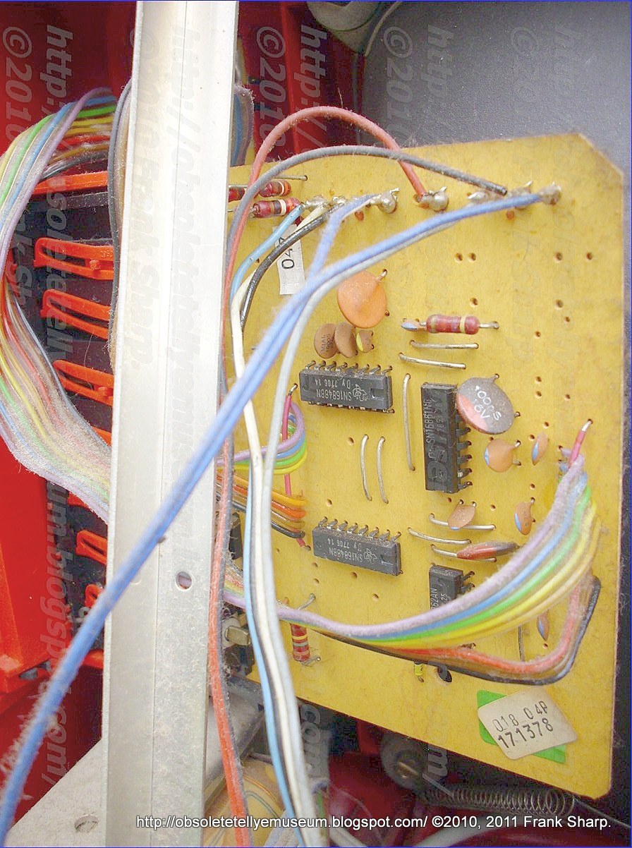
- SN16848BN
- SN16861NG
- SN16862AN
 1.
A circuit arrangement for establishing, at the chassis of an
electrical device powered by a grounded AC supply network, a reference
potential with relation to ground, said device having at least one
contactless touching switch operating on the AC voltage principle,
the switch being operated by touching a unipole touching field in a
contactless manner, said arrangement comprising an electronic
switch for selectively blocking the circuit of the device from the
supply network, a half-wave rectifier including a pair of diodes
individually connected in series-aiding relation between the
terminals of the supply network and the terminals of the device for
separating the electronic blocking switch from the supply network
during a blocking phase defined by a prescribed half period of the
AC cycle, and a pair of condensers individually connected in
parallel with the respective diodes.
2. A circuit arrangement according to claim 1, wherein the
capacitances of the two condensers are of equal magnitude.
1.
A circuit arrangement for establishing, at the chassis of an
electrical device powered by a grounded AC supply network, a reference
potential with relation to ground, said device having at least one
contactless touching switch operating on the AC voltage principle,
the switch being operated by touching a unipole touching field in a
contactless manner, said arrangement comprising an electronic
switch for selectively blocking the circuit of the device from the
supply network, a half-wave rectifier including a pair of diodes
individually connected in series-aiding relation between the
terminals of the supply network and the terminals of the device for
separating the electronic blocking switch from the supply network
during a blocking phase defined by a prescribed half period of the
AC cycle, and a pair of condensers individually connected in
parallel with the respective diodes.
2. A circuit arrangement according to claim 1, wherein the
capacitances of the two condensers are of equal magnitude.
Description:
This
invention relates to a circuit arrangement for establishing a
constant reference potential on the chassis of an electrical
instrument such as a radio and/or a TV receiver. Such instrument
includes at least one contactless touching switch operating under
the AC voltage principle, whereby by touching a single pole
touching field the contactless switch is operated.
In electronic devices, for example TV and radio receivers, there are used in ever increasing numbers electronic touching switches for switching and adjusting the functions of the device. In one known embodiment of this type of touching switch, which operates on a DC voltage principle, the function of the electronic device, is contactlessly switched by touching a unipole touching field, the switching being carried out by means of an alternating current voltage. When using such a unipole touching electrode, one takes advantage of the fact that the AC current circuit is generally unipolarly grounded. In order to close the circuit by touching the touching surface via the body of the operator to ground, it is necessary to provide an AC voltage on the touching field. In one special known embodiment there is employed a known bridge current rectifier for the current supply. This type of arrangement has the drawback that the chassis of the device changes its polarity relative to the grounded network pole with the network frequency. With such construction considerable difficulties appear when connecting measuring instruments to the device, such difficulties possibly eventually leading to the destruction of individual parts of the electronic device.
In order to avoid these drawbacks, the present invention provides a normal combination of a unidirectional rectifier with an electronic blocking switch that separates the chassis of the electronic device from the network during the blocking phase. In accordance with the present invention, the polarity of the chassis of the electronic device does not periodically change, because the electronic device is practically separated from the network during the blocking phase of the unidirectional rectifier by means of the electronic blocking switch.
In a further embodiment of the invention a further rectifier is connected in series with the unidirectional rectifier in the connection between the circuit and the negative pole of the chassis. Such further rectifier is preferably a diode which is switched in the transfer direction of the unidirectional rectifier. According to another feature of the invention there are provided condensers, a respective condenser being connected parallel with each of the rectifiers. Preferably the two condensers have equal capacitances. Because of the use of such condensers, which are required because of high frequency reasons, during the blocking phase there is conducted to the chassis of the electronic device an AC voltage proportional to the order of capacitances of the condensers. Thus there is placed upon the touching field in a desired manner an AC voltage, and there is thereby assured a secure functioning of the adjustment of the device when such touching occurs.
I n
the embodiment of the invention employing two rectifiers there is
the further advantage that over a bridging over of the minus
conduit of the rectifier that is connected between the network and
the negative pole of the chassis connection, no injuries can be
caused by a measuring instrument in the electronic device itself
and in the circuit arrangement connected thereto.
n
the embodiment of the invention employing two rectifiers there is
the further advantage that over a bridging over of the minus
conduit of the rectifier that is connected between the network and
the negative pole of the chassis connection, no injuries can be
caused by a measuring instrument in the electronic device itself
and in the circuit arrangement connected thereto.
In the accompanying drawing:
The sole FIGURE of the drawing is a circuit diagram of a preferred embodiment of the invention.
In the illustrated embodiment the current supply part of the device, shown at the left, is connected via connecting terminals A and B to an AC voltage source, the terminal B being grounded at 8. The current supply part consists of a unidirectional rectifier in the form of a diode 1 with its anode connected to the terminal I, the cathode of diode 1 being connected to one input terminal 9 of an electronic device 2. In the device 2 there is also arranged a sensor circuit 3, shown here mainly as a block, circuit 3 being shown as including a pnp input transistor the emitter of which is connected to an output terminal 11 of the device 2. The collector of such transistor is connected to the other output terminal 12 of the device 2. The base of the transistor is connected by a wire 13 to a unipolar touching field 4 which may be in the form of a simple metal plate instead of the pnp transistor shown, the sensor circuit itself may consist of a standard integrating circuit which controls, among other things, the periodic sequential switching during the touching time of the touching field 4. All of the circuits of the electronic device 2 are isolated in a known manner from the chassis potential. Between the network terminal B and the negative pole 10 of the chassis there is arranged in the direction opposite that of diode 1 a further diode 5, the anode of diode 5 being connected to the terminal 10, and the cathode of diode 5 being connected to the terminal B of the current supply. To provide for HF type bridging of the diodes 1 and 5 there are arranged condensers 6 and 7 respectively, which are connected in parallel with such diodes.
The
invention functions by reason of the fact that in an AC network
separate devices radiate electromagnetic waves which produce freely
traveling fields in the body of the person who is operating and/or
adjusting the device, thereby producing an alternating current
through his body to ground, as indicated by the - line at the right
of the circuit diagram. If now the person operating the device
touches the switching field 4, then the pnp type input transistor of
the sensor circuit 3, which is placed on a definite reference
potential (for example 12 Volts) and is connected with the negative
halfwave of the AC voltage potential, is made conductive. There is
thereby released a control command in the sequential switching, for
example, for switching the electronic device to the next receiving
channel. It is understood that the most suitable connection is
formed between ground and the touching field 4 by means of a wire.
By the use of such wires it would be assured that in all cases the
base of the transistor in circuit 3 is connected to ground. This
would, however, not permit anyone to operate the switch without the
use of an auxiliary means such as a wire. It will be assumed that
the touching almost always results directly via the almost isolated
human body. For this reason the AC current fields are necessary,
because otherwise there cannot always be provided a ground contact.
Thus this connection is established via the body resistance of the
person carrying out the touching of the switch.
The positive half wave of the alternating current travels to the terminal 9 of the electronic device 2 after such current has been rectified and smoothed by the devices 1, 6. Such positive halfwave is also conducted to the sensor circuit 3. The thus formed current circuit is closed by way of the chassis of the electronic device 3, the diode 5, and the terminal B. When there is a negative halfwave of the alternating current delivered by the current supply, both diodes 1 and 5 remain closed so that the chassis of the device 2 remains separated from the network during the blocking phase. Nevertheless, by means of condensers 6 and 7 the chassis is placed in a definite network potential, which depends on the relationship of the order of magnitude of the two condensers 6 and 7. When the capacitances of such condensers are equal, there is placed upon the chassis of the device 2 the constant reference potential, and simultaneously there is present via the sensor circuit 3 the required AC voltage at the touching field 4 for adjusting the function or functions of the device 2 upon the touching of the touching field 4.
The reference character 15 indicates a terminal or point at which the potential of the chassis of the device 2 may be measured. As above explained, the diode 5 causes the potential of the chassis at 15 to be separated from the network ground when a negative AC halfwave arrives. It will be noted that the return conduit of the circuit is held at a fixed chassis potential. The input transistor of the sensor circuit 3 remains, however, locked because it is subjected to a DC current of about 12 volts. If now, by means of touching the touching field 4, the chassis potential is connected to ground, then the transistor switches through and releases a switching function.
If the connecting terminals AB of the current source are exchanged, as by changing the plug, then there is still secured the condition that the chassis of the device is separated from the network ground via the diode, in this case the diode 1. The reference potential of the chassis consequently remains constant and the changing AC fields which are superimposed on the condensers can produce in the touching human body an AC current voltage due to the fields which are radiated by the device.
A suitable sensor which may be employed for the circuit 3 herein may be a sensor known as the "SAS 560 Tastatur IS," manufactured and sold by Siemens AG.
It is to be understood that the present invention is not limited to the illustrated environment. They can also be used in electronic blocking switch including a Thyristor circuit, which in the same manner separates the electronic device during the blocking phase from the network rectifier. With such Thyristor circuit the drawbacks described in the introductory portion of the specification of known circuit arrangements are also avoided.
Although the invention is illustrated and described with reference to a plurality of preferred embodiments thereof, it is to be expressly understood that it is in no way limited to the disclosure of such a plurality of preferred embodiments, but is capable of numerous modifications within the scope of the appended claims.
In electronic devices, for example TV and radio receivers, there are used in ever increasing numbers electronic touching switches for switching and adjusting the functions of the device. In one known embodiment of this type of touching switch, which operates on a DC voltage principle, the function of the electronic device, is contactlessly switched by touching a unipole touching field, the switching being carried out by means of an alternating current voltage. When using such a unipole touching electrode, one takes advantage of the fact that the AC current circuit is generally unipolarly grounded. In order to close the circuit by touching the touching surface via the body of the operator to ground, it is necessary to provide an AC voltage on the touching field. In one special known embodiment there is employed a known bridge current rectifier for the current supply. This type of arrangement has the drawback that the chassis of the device changes its polarity relative to the grounded network pole with the network frequency. With such construction considerable difficulties appear when connecting measuring instruments to the device, such difficulties possibly eventually leading to the destruction of individual parts of the electronic device.
In order to avoid these drawbacks, the present invention provides a normal combination of a unidirectional rectifier with an electronic blocking switch that separates the chassis of the electronic device from the network during the blocking phase. In accordance with the present invention, the polarity of the chassis of the electronic device does not periodically change, because the electronic device is practically separated from the network during the blocking phase of the unidirectional rectifier by means of the electronic blocking switch.
In a further embodiment of the invention a further rectifier is connected in series with the unidirectional rectifier in the connection between the circuit and the negative pole of the chassis. Such further rectifier is preferably a diode which is switched in the transfer direction of the unidirectional rectifier. According to another feature of the invention there are provided condensers, a respective condenser being connected parallel with each of the rectifiers. Preferably the two condensers have equal capacitances. Because of the use of such condensers, which are required because of high frequency reasons, during the blocking phase there is conducted to the chassis of the electronic device an AC voltage proportional to the order of capacitances of the condensers. Thus there is placed upon the touching field in a desired manner an AC voltage, and there is thereby assured a secure functioning of the adjustment of the device when such touching occurs.
I
n
the embodiment of the invention employing two rectifiers there is
the further advantage that over a bridging over of the minus
conduit of the rectifier that is connected between the network and
the negative pole of the chassis connection, no injuries can be
caused by a measuring instrument in the electronic device itself
and in the circuit arrangement connected thereto.In the accompanying drawing:
The sole FIGURE of the drawing is a circuit diagram of a preferred embodiment of the invention.
In the illustrated embodiment the current supply part of the device, shown at the left, is connected via connecting terminals A and B to an AC voltage source, the terminal B being grounded at 8. The current supply part consists of a unidirectional rectifier in the form of a diode 1 with its anode connected to the terminal I, the cathode of diode 1 being connected to one input terminal 9 of an electronic device 2. In the device 2 there is also arranged a sensor circuit 3, shown here mainly as a block, circuit 3 being shown as including a pnp input transistor the emitter of which is connected to an output terminal 11 of the device 2. The collector of such transistor is connected to the other output terminal 12 of the device 2. The base of the transistor is connected by a wire 13 to a unipolar touching field 4 which may be in the form of a simple metal plate instead of the pnp transistor shown, the sensor circuit itself may consist of a standard integrating circuit which controls, among other things, the periodic sequential switching during the touching time of the touching field 4. All of the circuits of the electronic device 2 are isolated in a known manner from the chassis potential. Between the network terminal B and the negative pole 10 of the chassis there is arranged in the direction opposite that of diode 1 a further diode 5, the anode of diode 5 being connected to the terminal 10, and the cathode of diode 5 being connected to the terminal B of the current supply. To provide for HF type bridging of the diodes 1 and 5 there are arranged condensers 6 and 7 respectively, which are connected in parallel with such diodes.
The
invention functions by reason of the fact that in an AC network
separate devices radiate electromagnetic waves which produce freely
traveling fields in the body of the person who is operating and/or
adjusting the device, thereby producing an alternating current
through his body to ground, as indicated by the - line at the right
of the circuit diagram. If now the person operating the device
touches the switching field 4, then the pnp type input transistor of
the sensor circuit 3, which is placed on a definite reference
potential (for example 12 Volts) and is connected with the negative
halfwave of the AC voltage potential, is made conductive. There is
thereby released a control command in the sequential switching, for
example, for switching the electronic device to the next receiving
channel. It is understood that the most suitable connection is
formed between ground and the touching field 4 by means of a wire.
By the use of such wires it would be assured that in all cases the
base of the transistor in circuit 3 is connected to ground. This
would, however, not permit anyone to operate the switch without the
use of an auxiliary means such as a wire. It will be assumed that
the touching almost always results directly via the almost isolated
human body. For this reason the AC current fields are necessary,
because otherwise there cannot always be provided a ground contact.
Thus this connection is established via the body resistance of the
person carrying out the touching of the switch.The positive half wave of the alternating current travels to the terminal 9 of the electronic device 2 after such current has been rectified and smoothed by the devices 1, 6. Such positive halfwave is also conducted to the sensor circuit 3. The thus formed current circuit is closed by way of the chassis of the electronic device 3, the diode 5, and the terminal B. When there is a negative halfwave of the alternating current delivered by the current supply, both diodes 1 and 5 remain closed so that the chassis of the device 2 remains separated from the network during the blocking phase. Nevertheless, by means of condensers 6 and 7 the chassis is placed in a definite network potential, which depends on the relationship of the order of magnitude of the two condensers 6 and 7. When the capacitances of such condensers are equal, there is placed upon the chassis of the device 2 the constant reference potential, and simultaneously there is present via the sensor circuit 3 the required AC voltage at the touching field 4 for adjusting the function or functions of the device 2 upon the touching of the touching field 4.
The reference character 15 indicates a terminal or point at which the potential of the chassis of the device 2 may be measured. As above explained, the diode 5 causes the potential of the chassis at 15 to be separated from the network ground when a negative AC halfwave arrives. It will be noted that the return conduit of the circuit is held at a fixed chassis potential. The input transistor of the sensor circuit 3 remains, however, locked because it is subjected to a DC current of about 12 volts. If now, by means of touching the touching field 4, the chassis potential is connected to ground, then the transistor switches through and releases a switching function.
If the connecting terminals AB of the current source are exchanged, as by changing the plug, then there is still secured the condition that the chassis of the device is separated from the network ground via the diode, in this case the diode 1. The reference potential of the chassis consequently remains constant and the changing AC fields which are superimposed on the condensers can produce in the touching human body an AC current voltage due to the fields which are radiated by the device.
A suitable sensor which may be employed for the circuit 3 herein may be a sensor known as the "SAS 560 Tastatur IS," manufactured and sold by Siemens AG.
It is to be understood that the present invention is not limited to the illustrated environment. They can also be used in electronic blocking switch including a Thyristor circuit, which in the same manner separates the electronic device during the blocking phase from the network rectifier. With such Thyristor circuit the drawbacks described in the introductory portion of the specification of known circuit arrangements are also avoided.
Although the invention is illustrated and described with reference to a plurality of preferred embodiments thereof, it is to be expressly understood that it is in no way limited to the disclosure of such a plurality of preferred embodiments, but is capable of numerous modifications within the scope of the appended claims.
No comments:
Post a Comment
The most important thing to remember about the Comment Rules is this:
The determination of whether any comment is in compliance is at the sole discretion of this blog’s owner.
Comments on this blog may be blocked or deleted at any time.
Fair people are getting fair reply. Spam and useless crap and filthy comments / scrapers / observations goes all directly to My Private HELL without even appearing in public !!!
The fact that a comment is permitted in no way constitutes an endorsement of any view expressed, fact alleged, or link provided in that comment by the administrator of this site.
This means that there may be a delay between the submission and the eventual appearance of your comment.
Requiring blog comments to obey well-defined rules does not infringe on the free speech of commenters.
Resisting the tide of post-modernity may be difficult, but I will attempt it anyway.
Your choice.........Live or DIE.
That indeed is where your liberty lies.
Note: Only a member of this blog may post a comment.