


The CHASSIS ELCIT T301 EPM 32 687 341 301/P is an example of simplicity and reliability + quality toghether.
The only weak point in this chassis was / is the line output EHT Transformer. The original fails but was easy to replace like here shown and no problems developed after.
Pictures produced are at very high contrast and bright and they're far superior than many other brands /model even more expensive.
It' s almost entirely based around PHILIPS Semicondutors technology except for the Power supply which is based on SIEMENS semiconductors.


Power supply Description based on TDA4601d (SIEMENS)

 TDA4601 Operation. * The TDA4601 device is a single in line, 9 pin chip. Its predecessor was the TDA4600 device, the TDA4601 however has improved switching, better protection and cooler running. The (SIEMENS) TDA4601 power supply is a fairly standard parallel chopper switch mode type, which operates on the same basic principle as a line output stage. It is turned on and off by a square wave drive pulse, when switched on energy is stored in the chopper transformer primary winding in the form of a magnetic flux; when the chopper is turned off the magnetic flux collapses, causing a large back emf to be produced. At the secondary side of the chopper transformer this is rectified and smoothed for H.T. supply purposes. The advantage of this type of supply is that the high chopping frequency (20 to 70 KHz according to load) allows the use of relatively small H.T. smoothing capacitors making smoothing easier. Also should the chopper device go short circuit there is no H.T. output. In order to start up the TDA4601 I.C. an initial supply of 9v is required at pin 9, this voltage is sourced via R818 and D805 from the AC side of the bridge rectifier D801, also pin 5 requires a +Ve bias for the internal logic block. (On some sets pin 5 is used for standby switching). Once the power supply is up and running, the voltage on pin 9 is increased to 16v and maintained at this level by D807 and C820 acting as a half wave rectifier and smoothing circuit. PIN DESCRIPTIONS Pin 1 This is a 4v reference produced within the I.C. Pin 2 This pin detects the exact point at which energy stored in the chopper transformer collapses to zero via R824 and R825, and allows Q1 to deliver drive volts to the chopper transistor. It also opens the switch at pin 4 allowing the external capacitor C813 to charge from its external feed resistor R810. Pin 3 H.T. control/feedback via photo coupler D830. The voltage at this pin controls the on time of the chopper transistor and hence the output voltage. Normally it runs at Approximately 2v and regulates H.T. by sensing a proportion of the +4v reference at pin 1, offset by conduction of the photo coupler D830 which acts like a variable resistor. An increase in the conduction of transistor D830 and therefor a reduction of its resistance will cause a corresponding reduction of the positive voltage at Pin 3. A decrease in this voltage will result in a shorter on time for the chopper transistor and therefor a lowering of the output voltage and vice versa, oscillation frequency also varies according to load, the higher the load the lower the frequency etc. should the voltage at pin 3 exceed 2.3v an internal flip flop is triggered causing the chopper drive mark space ratio to extend to 244 (off time) to 1 (on time), the chip is now in over volts trip condition. Pin 4 At this pin a sawtooth waveform is generated which simulates chopper current, it is produced by a time constant network R810 and C813. C813 charges when the chopper is on and is discharged when the chopper is off, by an internal switch strapping pin 4 to the internal +2v reference, see Fig 2. The amplitude of the ramp is proportional to chopper drive. In an overload condition it reaches 4v amplitude at which point chopper drive is reduced to a mark-space ratio of 13 to 1, the chip is then in over current trip. The I.C. can easily withstand a short ci
Semiconductor circuit for supplying power to electrical equipment, comprising a transformer having a primary winding connected, via a parallel connection of a collector-emitter path of a transistor with a first capacitor, to both outputs of a rectifier circuit supplied, in turn, by a line a-c voltage; said transistor having a base controlled via a second capacitor by an output of a control circuit acted upon, in turn by the rectified a-c line voltage as actual value and by a reference voltage; said transformer having a first secondary winding to which the electrical equipment to be supplied is connected; said transformer having a second secondary winding with one terminal thereof connected to the emitter of said transistor and the other terminal thereof connected to an anode of a first diode leading to said control circuit; said transformer having a third secondary winding with one terminal thereof connected, on the one hand, via a series connection of a third capacitor with a first resistance, to the other terminal of said third secondary winding and connected, on the other hand, to the emitter of said transistor, the collector of which is connected to said primary winding; a point between said third capacitor and said first resistance being connected to the cathode of a second diode; said control circuit having nine terminals including a first terminal delivering a reference voltage and connected, via a voltage divider formed of a third and fourth series-connected resistances, to the anode of said second diode; a second terminal of said control circuit serving for zero-crossing identification being connected via a fifth resistance to said cathode of said second diode; a third terminal of said control-circuit serving as actual value input being directly connected to a divider point of said voltage divider forming said connection of said first terminal of said control circuit to said anode of said second diode; a fourth terminal of said control circuit delivering a sawtooth voltage being connected via a sixth resistance to a terminal of said primary winding of said transformer facing away from said transistor; a fifth terminal of said control circuit serving as a protective input being connected, via a seventh resistance to the cathode of said first diode and, through the intermediary of said seventh resistance and an eighth resistance, to the cathode of a third diode having an anode connected to an input of said rectifier circuit; a sixth terminal of said control circuit carrying said reference potential and being connected via a fourth capacitor to said fourth terminal of said control circuit and via a fifth capacitor to the anode of said second diode; a seventh terminal of said control circuit establishing a potential for pulses controlling said transistor being connected directly and an eighth terminal of said control circuit effecting pulse control of the base of said transistor being connected through the intermediary of a ninth resistance to said first capacitor leading to the base of said transistor; and a ninth terminal of said control circuit serving as a power supply input of said control circuit being connected both to the cathode of said first diode as well as via the intermediary of a sixth capacitor to a terminal of said second secondary winding as well as to a terminal of said third secondary winding.
Description:
The invention relates to a blocking oscillator type switching power supply for supplying power to electrical equipment, wherein the primary winding of a transformer, in series with the emitter-collector path of a first bipolar transistor, is connected to a d-c voltage obtained by rectification of a line a-c voltage fed-in via two external supply terminals, and a secondary winding of the transformer is provided for supplying power to the electrical equipment, wherein, furthermore, the first bipolar transistor has a base controlled by the output of a control circuit which is acted upon in turn by the rectified a-c line voltage as actual value and by a set-point transmitter, and wherein a starting circuit for further control of the base of the first bipolar transistor is provided. Such a blocking oscillator switching power supply is described in the German periodical, "Funkschau" (1975) No. 5, pages 40 to 44. It is well known that the purpose of such a circuit is to supply electronic equipment, for example, a television set, with stabilized and controlled supply voltages. Essential for such switching power supply is a power switching transistor i.e. a bipolar transistor with high switching speed and high reverse voltage. This transistor therefore constitutes an important component of the control element of the control circuit. Furthermore, a high operating frequency and a transformer intended for a high operating frequency are provided, because generally, a thorough separation of the equipment to be supplied from the supply naturally is desired. Such switching power supplies may be constructed either for synchronized or externally controlled operation or for non-synchronized or free-running operation. A blocking converter is understood to be a switching power supply in which power is delivered to the equipment to be supplied only if the switching transistor establishing the connection between the primary coil of the transformer and the rectified a-c voltage is cut off. The power delivered by the line rectifier to the primary coil of the transformer while the switching transistor is open, is interim-stored in the transformer and then delivered to the consumer on the secondary side of the transformer with the switching transistor cut off.
In the blocking converter described in the aforementioned reference in the literature, "Funkschau" (1975), No. 5, Pages 40 to 44, the power switching transistor is connected in the manner defined in the introduction to this application. In addition, a so-called starting circuit is provided. Because several diodes are generally provided in the overall circuit of a blocking oscillator according to the definition provided in the introduction hereto, it is necessary, in order not to damage these diodes, that due to the collector peak current in the case of a short circuit, no excessive stress of these diodes and possibly existing further sensitive circuit parts can occur.
Considering the operation of a blocking oscillator, this means that, in the event of a short circuit, the number of collector current pulses per unit time must be reduced. For this purpose, a control and regulating circuit is provided. Simultaneously, a starting circuit must bring the blocking converter back to normal operation when the equipment is switched on, and after disturbances, for example, in the event of a short circuit. The starting circuit shown in the literature reference "Funkschau" on Page 42 thereof, differs to some extent already from the conventional d-c starting circuits. It is commonly known for all heretofore known blocking oscillator circuits, however, that a thyristor or an equivalent circuit replacing the thyristor is essential for the operation of the control circuit.
It is accordingly an object of the invention to provide another starting circuit. It is a further object of the invention to provide a possible circuit for the control circuit which is particularly well suited for this purpose. It is yet another object of the invention to provide such a power supply which is assured of operation over the entire range of line voltages from 90 to 270 V a-c, while the secondary voltages and secondary load variations between no-load and short circuit are largely constant.
In accordance with another feature of the invention, there is provided a second bipolar transistor having the same conduction type as that of the first bipolar transistor and connected in the starting circuit with the base thereof connected to a cathode of a semiconductor diode, the semiconductor diode having an anode connected to the emitter of the first bipolar transistor, the second bipolar transistor having a collector connected via a resistor to a cathode of the first diode in the starting circuit, and having an emitter connected to the input serving to supply power to the control circuit and also connected to the cathode of the second diode which is connected to the other secondary winding of the transformer.
In accordance with a further feature of the invention, the base of the second bipolar transistor is connected to a resistor and via the latter to one pole of a first capacitor, the anode of the first diode being connected to the other pole of the first capacitor.
In accordance with an added feature of the invention, the input serving to supply power to the control circuit is connected via a second capacitor to an output of a line rectifier, the output of the line rectifier being directly connected to the emitter of the first bipolar transistor.
In accordance with an additional feature of the invention, the other secondary winding is connected at one end to the emitter of the first bipolar transistor and to a pole of a third capacitor, the third capacitor having another pole connected, on the one hand, via a resistor, to the other end of the other secondary winding and, on the other hand, to a cathode of a third diode, the third diode having an anode connected via a potentiometer to an actual value input of the control circuit and, via a fourth capacitor, to the emitter of the first bipolar transistor. In accordance with yet another feature of the invention, the control circuit has a control output connected via a fifth capacitor to the base of the first bipolar transistor for conducting to the latter control pulses generated in the control circuit.
In accordance with a concomitant feature of the invention, there is provided a sixth capacitor shunting the emitter-collector path of the first transistor.
Other features which are considered as characteristic for the invention are set forth in the appended claim.
Although the invention is illustrated and described herein as embodied in a blocking oscillator type switching power supply, it is nevertheless not intended to be limited to the details shown, since various modifications and structural changes may be made therein without departing from the spirit of the invention and within the scope and range of equivalents of the claims.
The TDA3562A is a monolithic IC designed as
decode PAL and/or NTSC colour television standards
and it combines all functions required for the
identification and demodulation of PAL and NTSC
signals.
.CHROMINANCE SIGNALPROCESSOR
.LUMINANCE SIGNAL PROCESSING WITH
CLAMPING
.HORIZONTAL AND VERTICAL BLANKING
.LINEAR TRANSMISSION OF INSERTED
RGB SIGNALS
.LINEAR CONTRAST AND BRIGHTNESS
CONTROL ACTING ON INSERTED AND MATRIXED
SIGNALS
.AUTOMATIC CUT-OFF CONTROL
.NTSC HUE CONTROL.
 CRT Line Output Stage Operation Principle:
 I'll examine the operation of the line output stage, whose basic job is to generate a sawtooth current in the line scan coils so that the beams are deflected horizontally across the picture tube's screen. The beams are deflected from the left-hand side to the right-hand side to give the forward line scan: this is followed by a rapid, blanked flyback to the left-hand side ready to trace out the next viewed line. Because of the way in which the flyback is achieved, the line output transformer generates various pulse voltages which are rectified to produce the e.h.t. required by the tube and other supplies. The line output stage is not just any sort of amplifier. The active device, almost always a transistor though valves, thyristors and gate -controlled switches have been used in the past, operates as a switch, the inductive components in the stage being mainly responsible for generating the sawtooth current waveform. Tuning is used to generate and control the flyback. The line drive waveform controls the output transistor's on/off switching and thus determines the timing of the cycle of operations, keeping them phase synchronised with the transmitted picture signal.
Basic Operation
Fig. 1 shows in most basic form the main elements in the line output stage, the active device (transistor) being shown as a switch. When the switch is closed, capacitor C and diode D are shorted out and the 150V supply is connected across coil L. Now it's a basic law of inductance that when a d.c. voltage is connected across a coil the current flowing through the coil builds up linearly from zero. Fig. 2(a) shows this as a positive -going ramp that starts at time t 1 , when the switch is closed. After about 26psec (t2), roughly the time required to deflect the beams from screen centre flows via the large -value capacitor CR, charging the tuning capacitor C with the result that the voltage at its 'upper' plate (the one connected to the coil) rises to a relatively high positive value. When all the energy in coil L has been transferred to capacitor C (time t3) the latter begi
 ns
to discharge, passing the energy back the other way to L via CR which,
as far as the circuit's a.c. operation is concerned, can be regarded as a
short-circuit. At time t4 the capacitor has discharged, having
transferred the energy back to the coil. This to-and-fro interchange of
energy between L and C, which from the a.c. point of view are in
parallel (CR representing a short-circuit), is the normal action of a
tuned/resonant/oscillatory circuit. The resonant frequency is determined
by the values of L and C. These are selected so that when time t4 is
reached, i.e. after a half cycle of oscillation, the sawtooth current
has passed through zero to a negative point on the ramp and the beams
have been deflected to the left-hand side of the screen ready for the
next active line scan. To complete the oscillatory cycle (the normal
resonant circuit action) the voltage at the upper plate of capacitor C
would have to move negatively with respect to chassis. It can't do so
because of the presence of diode D, which is called the efficiency diode
- we'll explain that in a minute. When the voltage at the cathode of D
tries to swing negatively it conducts, i.e. switches on, providing a
discharge path for the coil. Once again because of the inductance in the
circuit there's a gradual, linear current discharge, the enegery being
returned to the supply's reservoir capacitor CR. During this discharge,
the beams are deflected back towards the centre of the screen (times t4
to t5). At this point the magnetic flux (energy) in L has been
dissipated. C is still in its discharged state, being shorted out by
diode D. So at time t5, with the beams at screen centre (zero
deflection), the switch has to be closed so that the cycle of operation
can be repeated. The action of diode D has, with the inductance in the
circuit, provided half the scan power while in the process returning the
energy (minus inevitable circuit losses) to the reservoir capacitor. No
wonder it's called the efficiency diode. It's important to note that
the beam flyback period t2 to t4 is governed by the time -constant of L
and C, consisting of one half cycle of oscillation. To achieve a flyback
time of 12μsec the duration of one cycle needs to be 24μsec: so the
resonant frequency of L and C works out at 41.67kHz. Fig. 3 illustrates
the four phases in the operation of the line output stage. Now the
voltage developed across an inductor is propor- tional to the rate of
change of the current flowing through it. Thus the voltage across L is
relatively low during the forward scan period but correspondingly high
during the flyback, when the current flow is faster because of the
circuit resonance. The voltage developed at the positive plate of
capacitor C is shown in Fig. 2(b), typically peaking at 1,200V. Both the
line output transistor and the efficiency diode must be capable of
withstanding this high reverse voltage. As we've seen, the circuit
action is highly efficient as the energy stored in L is returned to the
supply during the first half of the forward scan: indeed with 'perfect'
components there would be no net demand on the power supply at all! In
practice because of the resistance of the inductor and the losses in the
diode, switch and capacitor the circuit takes out a little more than it
puts back, while the practice of loading the transformer with rectifier
circuits to provide power for other sections of the set increases the
stage's current demand. To make up for these losses, the line output
transistor is switched on slightly before instead of at the centre of
the forward scan. In a practical circuit L is the primary winding of the
line output transformer and the deflection coils are connected across
it via a d.c. blocking capacitor, CB, as shown in Fig. 4. This coupling
capacitor also provides scan -correction (often referred to as S
-correction). Why is this required? If a linear deflection current was
used to control the scanning with a relatively flat -faced picture tube
the sides of the picture would be stretched out in comparison with the
centre section. Hence S -correction: the value of the coupling capacitor
is chosen so that it resonantes with the inductance of the scan coils
at about 5kHz. This has the effect of adding a sinewave component to the
sawtooth current, as shown in
Fig. 5. Thus the deflection power is tailored to suit the length of the
beam paths as the screen is scanned, correcting the horizontal
linearity of the display. At the line scanning frequency the scan coils
behave as an almost perfect inductor, but their small d.c. resistance is
in series with the fixed voltage that should be present across the
coil. It has the effect of introducing an asymmetric sensitivity loss
during the forward scan. To counteract it a further component is added
in series with the scan coils - an inductor with a saturable magnetic
core, biased by a permanent magnet so that its inductance falls as the
scan current increases. The voltage drop across this inductor, which is
known as the linearity coil, varies in the opposite sense to that
produced by the resistance of the coils, thus providing an equal -but
-opposite cancellation effect. In some TV sets the permanent magnet can
be adjusted to trim the linearity correction, though many modern sets
use components with such tight tolerances that a sealed linearity
-correction coil can be used. With some very small -screen sets the
horizontal non -linearity effect is small enough to be ignored.
ns
to discharge, passing the energy back the other way to L via CR which,
as far as the circuit's a.c. operation is concerned, can be regarded as a
short-circuit. At time t4 the capacitor has discharged, having
transferred the energy back to the coil. This to-and-fro interchange of
energy between L and C, which from the a.c. point of view are in
parallel (CR representing a short-circuit), is the normal action of a
tuned/resonant/oscillatory circuit. The resonant frequency is determined
by the values of L and C. These are selected so that when time t4 is
reached, i.e. after a half cycle of oscillation, the sawtooth current
has passed through zero to a negative point on the ramp and the beams
have been deflected to the left-hand side of the screen ready for the
next active line scan. To complete the oscillatory cycle (the normal
resonant circuit action) the voltage at the upper plate of capacitor C
would have to move negatively with respect to chassis. It can't do so
because of the presence of diode D, which is called the efficiency diode
- we'll explain that in a minute. When the voltage at the cathode of D
tries to swing negatively it conducts, i.e. switches on, providing a
discharge path for the coil. Once again because of the inductance in the
circuit there's a gradual, linear current discharge, the enegery being
returned to the supply's reservoir capacitor CR. During this discharge,
the beams are deflected back towards the centre of the screen (times t4
to t5). At this point the magnetic flux (energy) in L has been
dissipated. C is still in its discharged state, being shorted out by
diode D. So at time t5, with the beams at screen centre (zero
deflection), the switch has to be closed so that the cycle of operation
can be repeated. The action of diode D has, with the inductance in the
circuit, provided half the scan power while in the process returning the
energy (minus inevitable circuit losses) to the reservoir capacitor. No
wonder it's called the efficiency diode. It's important to note that
the beam flyback period t2 to t4 is governed by the time -constant of L
and C, consisting of one half cycle of oscillation. To achieve a flyback
time of 12μsec the duration of one cycle needs to be 24μsec: so the
resonant frequency of L and C works out at 41.67kHz. Fig. 3 illustrates
the four phases in the operation of the line output stage. Now the
voltage developed across an inductor is propor- tional to the rate of
change of the current flowing through it. Thus the voltage across L is
relatively low during the forward scan period but correspondingly high
during the flyback, when the current flow is faster because of the
circuit resonance. The voltage developed at the positive plate of
capacitor C is shown in Fig. 2(b), typically peaking at 1,200V. Both the
line output transistor and the efficiency diode must be capable of
withstanding this high reverse voltage. As we've seen, the circuit
action is highly efficient as the energy stored in L is returned to the
supply during the first half of the forward scan: indeed with 'perfect'
components there would be no net demand on the power supply at all! In
practice because of the resistance of the inductor and the losses in the
diode, switch and capacitor the circuit takes out a little more than it
puts back, while the practice of loading the transformer with rectifier
circuits to provide power for other sections of the set increases the
stage's current demand. To make up for these losses, the line output
transistor is switched on slightly before instead of at the centre of
the forward scan. In a practical circuit L is the primary winding of the
line output transformer and the deflection coils are connected across
it via a d.c. blocking capacitor, CB, as shown in Fig. 4. This coupling
capacitor also provides scan -correction (often referred to as S
-correction). Why is this required? If a linear deflection current was
used to control the scanning with a relatively flat -faced picture tube
the sides of the picture would be stretched out in comparison with the
centre section. Hence S -correction: the value of the coupling capacitor
is chosen so that it resonantes with the inductance of the scan coils
at about 5kHz. This has the effect of adding a sinewave component to the
sawtooth current, as shown in
Fig. 5. Thus the deflection power is tailored to suit the length of the
beam paths as the screen is scanned, correcting the horizontal
linearity of the display. At the line scanning frequency the scan coils
behave as an almost perfect inductor, but their small d.c. resistance is
in series with the fixed voltage that should be present across the
coil. It has the effect of introducing an asymmetric sensitivity loss
during the forward scan. To counteract it a further component is added
in series with the scan coils - an inductor with a saturable magnetic
core, biased by a permanent magnet so that its inductance falls as the
scan current increases. The voltage drop across this inductor, which is
known as the linearity coil, varies in the opposite sense to that
produced by the resistance of the coils, thus providing an equal -but
-opposite cancellation effect. In some TV sets the permanent magnet can
be adjusted to trim the linearity correction, though many modern sets
use components with such tight tolerances that a sealed linearity
-correction coil can be used. With some very small -screen sets the
horizontal non -linearity effect is small enough to be ignored.Practical Line Output Stage

Fig. 6 shows a relatively simple line output stage circuit used with a 90° -deflection tube. Tr5 is the line output transistor, which incorporates the efficiency diode in the same package. The primary winding of the line output trans- former T4 is the section between pins 2 and 10, C95 being the flyback tuning capacitor. Scan coil coupling and S - correction are provided by C94, the line linearity coil L14 being connected in series on the chassis side of the scan current path. L14 is damped by R110 to prevent it ringing when the line flyback pulse occurs - the effect of an undamped linearity coil is velocity modulation of the beams at the beginning of their sweeps, showing up as black -and - white vertical striations at the left-hand side of the screen. C92 is the reservoir capacitor, the h.t. feed being via 8105. 8106 and R109 feed pulses to the second phase -locked loop (APC2) in the sync chip - we dealt with this in last month's instalment. A second pulse feed from the same point goes to the colour decoder chip to provide line blanking, burst gating and PAL switch drive - this particular set doesn't use the sandcastle pulse approach.
Secondary Supplies
So much for the generation and control of the sawtooth scanning current. The rest of the components in this circuit are used to harness the energy in the transformer to provide power supplies for other sections of the receiver. The winding between pins 4 and 8 pulse energises the picture tube's heaters at 6.3V r.m.s. The other supplies make use of the transformer as the heart of a d.c.-to-d.c. converter system, by means of secondary windings that provide pulse feeds to diode/capacitor rectifier circuits. Small -value (0.680) resistors in the 25V and 200V supplies provide surge limiting and protection (by going open -circuit) in the event of a short-circuit in one of these supplies. The most significant supply is obtained from the diode - split winding that starts at pin 9. Although not shown in full detail it consists of several 'cells', each of which consists of an electrically isolated secondary winding, a built-in high - voltage rectifier diode and, as the reservoir capacitor, the carefully contrived capacitance that's present between adjacent, highly -insulated winding layers. These cells are connected in series to form a voltage -multiplier system capable of providing an e.h.t. supply for the tube's final anode of typically 24kV - it may be as high as 30kV in some designs. There's a built-in surge limiter resistor at the output end of the chain of cells. An important part of the e.h.t. multiplier system is the final reservoir capacitor that split chain provides about 8kV to a built-in potential -divider chain that contains two pres
ets:
the one at the top provides the supply for the tube's focus electrode
while the one near the bottom provides its first anode supply of about
800V. The bottom of the diode -split chain (pin 9) is returned to
chassis via a diode/capacitor/resistor network (not shown here). The
voltage developed across this network is proportional to the total beam
current, since this flows from the tube's cathodes via the e.h.t.
connector and the diode -split chain to chassis. Above a certain
threshold the voltage at pin 9 reduces the picture brightness and/or
contrast via the colour decoder/matrixing chip, limiting the beam
current and hence the dissipation in the tube's shadowmask to safe
levels. The winding between pins 10 and 7 of the transformer produces
50-70V pulses that sit on the h.t. voltage present at pin 10. When
rectified by D23 and C100 a 200V supply is provided for the RGB output
stages that drive the tube's cathodes. Secondary winding 4-6 feeds D24
and C99 which provide a 25V supply for the field timebase. In some
designs supplies for the audio output stage and the signal sections of
the receiver are also obtained from the line output transformer: in this
particular chassis they are obtained from the chopper transformer in
the power supply instead. Incidentally there have been one or two
designs, the Ferguson/philco TX10 chassis being a well-known example,
where the e.h.t. is also obtained from the chopper transformer, the line
output transformer then acting mainly as a load for the line output
transistor. In earlier designs a separate diode - capacitor multiplier
unit (tripler) was fed from a single line output transformer overwiding
to provide the e.h.t.Scan Rectification
The e.h.t., focus and 200V supplies d
erived
from the transformer are relatively lightly loaded, i.e. no great
current demand is placed on them. They can therefore be obtained by
rectifying the pulses present during the flyback period (time t2 -t4 in
Fig. 2), which is about twenty per cent of the scan cycle. Where the
current demand is greater, e.g. in a supply for the field timebase or an
audio output stage, the phasing of the relevant transformer winding is
often arranged so that the rectifier diode conducts during the scan
rather than the flyback period. Although the voltage available is much
lower, it's present for a longer period (about eighty per cent of the
scan/duty cycle). As a result the output regulation is much better. The
relatively high peak reverse voltage has to be taken into account in the
rectifier diode's specification.EHT Regulation
The internal impedance of a diode -sp
lit
e.h.t. supply is typically about 1MOhm. Thus with a total beam current
of lmA, present when a bright picture is being displayed on a 22in.
picture tube, the e.h.t. voltage will drop by about 1kV or five per
cent. The result of this is some ballooning, i.e. increase in picture
size. Compensation can be provided by reducing the line scanning power.
Careful choice of the value of the resistor that feeds the line output
transformer - R105 in Fig. 6 - gives automatic compensation in the
horizontal direction, while deriving the supply for the field output
stage from the line output transformer tends to cancel out the
ballooning in the vertical plane. Various 'anti -breathing' arrangements
are used in TV receiver design. Most operate via the diode -modulator
circuit we'll come to shortly. With any line output stage circuit the
picture width and e.h.t. voltage depend on the stage's h.t. supply, so
this must be well regulated and set up correctly. In the circuit shown
in Fig. 6 the h.t. voltage has to be 119V with a 20in. tube and 145V
with a 22in. tube.Pincushion Distortion
The raster produced on an almost -flat faced picture tube by constant -amplitude scan currents has pincushion distortion at all four sides. This is because of the disparity between the image plane and the screen's profile - . As a general rule the deflection yokes used with modern 90° tubes have built-in correction for both NS (vertical) and EW (horizontal) pincushion distortion while 110° tubes (generally above 22in. screen size) have in -yoke correction for NS distortion but cannot fully compensate for the
 pincushion
effect at the sides of the screen. Thus with these the line scan
current has to be amplitude -modulated by a parabolic waveform at field
frequency as shown in Fig. 7. With present-day tube designs a modulation
depth of about seven per cent is required. the peak -to -peak scan
current being typically 4.1A at the top and bottom of the screen and
4.4A towards the centre of the screen, where the deflection power is
greatest. Amplitude modulation of the line scan current can be achieved
by including a saturable -reactance transformer in series with the scan
coils, but this is expensive. You could put a suitably -shaped ripple on
the supply to the line output stage, but the parabola would be
superimposed on any secondary supplies derived from the line output
transformer. The most widely used solution is to employ a diode -modu-
lator circuit, since this gives full control of the raster shape and
scan amplitude while providing a constant load current and flyback time.
pincushion
effect at the sides of the screen. Thus with these the line scan
current has to be amplitude -modulated by a parabolic waveform at field
frequency as shown in Fig. 7. With present-day tube designs a modulation
depth of about seven per cent is required. the peak -to -peak scan
current being typically 4.1A at the top and bottom of the screen and
4.4A towards the centre of the screen, where the deflection power is
greatest. Amplitude modulation of the line scan current can be achieved
by including a saturable -reactance transformer in series with the scan
coils, but this is expensive. You could put a suitably -shaped ripple on
the supply to the line output stage, but the parabola would be
superimposed on any secondary supplies derived from the line output
transformer. The most widely used solution is to employ a diode -modu-
lator circuit, since this gives full control of the raster shape and
scan amplitude while providing a constant load current and flyback time.The Diode Modulator

Fig. 8 shows the essence of a diode -modulator arrange- ment. The efficiency diode is split in two, DI and D2, which perform the same clamping action as before. The flyback tuning capacitor is also split in two, Cl and C2: the upper one tunes the transformer and scan coils (L1) as before while the lower one tunes a bridge coil, L2, via C4 to the same flyback frequency of about 42kHz. C3 is the scan coupling capacitor, which corresponds with CB in Fig. 4. Modulation is achieved by using transistor Tr2, whose conduction governs the scan width, to vary the load across C4. When Tr2 is off, the scan energy is shared between the the two series LC combinations C3/L1 and L2/C4. The charge on C3 and C4 is in the ratio of about 7:1, the scan current being reduced in proportion. When Tr2 is fully conductive, C4 is effectively shorted out and acquires no charge. Thus a greater proportion of the energy is present in C3/L1 and the scan current and picture width are increased. By varying the conduction of Tr2 during the forward scan in a parabolic manner, EW pincushion correction is achieved. The basic picture width can be controlled by varying Tr2's standing bias. Choke L3 and the large -value capacitor
C5
filter the line -frequency energy so that it doesn't reach Tr2. And
because both sections of the load (L 1/C1 and L2/C2) are individually
tuned to the flyback frequency the flyback time, and hence the e.h.t.
and the other line output transformer -derived supplies, remain constant
over the field period despite the line scan current variation. There
are several different versions of the diode -modu- lator arrangement.
Some tube/yoke combinations have a scan -geometry characteristic such
that when the line scan current is modulated by a simple parabolic
waveform as described above the raster has inner pincushion distortion
as shown in Fig. 9.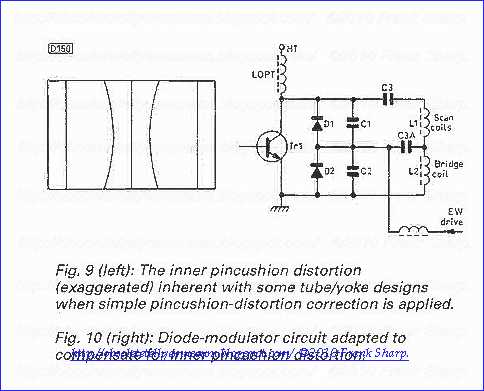 Because
of this. the EW-correction system also has to modulate the S
-correction. Fig. 10 shows, in skeleton circuit form. how this can be
done. There are two coupling/S-correction capacitors. C3 and C3A. C3 is
the usual S -correction capacitor, but C3A has an increasing influence
as the diode modulator begins to have maximum effect towards the centre
of the screen. Critical choice of the value of C3A ensures that the
inner curved verticals shown in Fig. 9 are straightened out to give a
raster completely free from geometric distortion. Although all diode
modulators work on the same basic principle, in some designs a
transformer is used in place of the bridge coil to give better impedance
matching and balance. Fig. 11 shows such an arrangement, used by Bang
and Olufsen. The EW correction waveform is applied to transformer T6.
whose winding 1-2 takes the place of L2 in Figs. 8 and 10. This circuit
also provides inner -pincushion distortion correction as just described,
the supplementary S - correction capacitor being C36.
Because
of this. the EW-correction system also has to modulate the S
-correction. Fig. 10 shows, in skeleton circuit form. how this can be
done. There are two coupling/S-correction capacitors. C3 and C3A. C3 is
the usual S -correction capacitor, but C3A has an increasing influence
as the diode modulator begins to have maximum effect towards the centre
of the screen. Critical choice of the value of C3A ensures that the
inner curved verticals shown in Fig. 9 are straightened out to give a
raster completely free from geometric distortion. Although all diode
modulators work on the same basic principle, in some designs a
transformer is used in place of the bridge coil to give better impedance
matching and balance. Fig. 11 shows such an arrangement, used by Bang
and Olufsen. The EW correction waveform is applied to transformer T6.
whose winding 1-2 takes the place of L2 in Figs. 8 and 10. This circuit
also provides inner -pincushion distortion correction as just described,
the supplementary S - correction capacitor being C36.Diode Modulator Drive

The parabolic EW drive waveform required is easily obtained by feeding the field -scan sawtooth waveform to a double integrator. By adding a sawtooth component the shape of the parabolic waveform can be tilted in either direction to give keystone -distortion correction if required - this is not generally necessary with modern tube/yoke designs. These EW correction characteristics are adjustable by preset resistors or, in the case of bus -programmable sets, remote control commands to the deflection processor. Very often the EW modulator is used to correct the previously mentioned picture breathing effect: this is done by feeding to the EW modulator's control circuit a voltage that's proportional to beam current.


RADIOMARELLI VEGA 24 " CHASSIS ELCIT T301 EPM 32 (687 341 301/P) THE PHILIPS TDA3562A Circuit arrangement for the control of a picture tube :
1. Circuit arrangement for the control of at least one beam current in a picture tube by a picture comprising
a control loop which in one sampling interval obtains a measuring signal from the value of the beam current on the occurrence of a given reference level in the picture signal, stores a control signal derived therefrom until the next sampling interval and thereby adjusts the beam current to a value preset by a reference signal.
and a trigger circuit which suppresses auxiliary pulses used to generate the beam current after the picture tube has been started up and issues a switching signal for the purpose of closing the control loop during the sampling intervals and for releasing the control of the beam current by the picture signal after the measuring signal has exceeded the threshold value,
a change detection arrangement which delivers a change signal when the stored signal has assumed a largely constant value, and
a logic network which does not release the control of the beam current by the picture signal outside the sampling intervals until the change signal has also been issued after the switching signal.
2. Circuit arrangement as set forth in claim 1, in which the picture signal comprises several color signals for the control of a corresponding number of beam currents for the display of a color picture in the picture tube and the control loop stores a part measuring signal or a part control signal derived therefrom for each color signal, characterized in that the change detection arrangement includes a change detector for each color signal which delivers a part change signal when the relevant stored signal has assumed a largely constant value, and the logic network does not release the control of the beam currents by the color signals outside the sampling intervals until the part change signals have been delivered by all change detectors.
3. Circuit arrangement as set forth in claim 1, including a comparator arrangement which compares the measuring signal with the reference signal and derives the control signal from this comparison, characterized in that the change detection arrangement detects a change in the control signal with respect to time and issues the change signal when the control signal has assumed a largely constant value.
4. Circuit arrangement as set forth in claims 1, 2, 3 including a control signal memory which contains at least one capacitor, characterized in that the change de
tection arrangement delivers the change signal when a charge-reversing current of the capacitor occuring during the starting up of the picture tube falls below a limit value.
5. Circuit arrangement as set forth in claim 2, including a comparator arrangement which compares the measuring signal with the reference signal and derives the control signal from this comparison, characterized in that the change detection arrangement detects a change in the control signal with respect to time and issues the change signal when the control signal has assumed a largely constant value.
BACKGROUND OF THE INVENTION
The invention relates to a circuit arrangement for the control of at least one beam current in a picture tube by a picture signal with a control loop which in one sampling interval obtains a measuring signal from the value of the beam current on the occurrence of a given reference level in the picture signal, stores a control signal derived therefrom until the next sampling interval and by this means adjusts the beam current to a value preset by a reference signal, and with a trigger circuit which suppresses auxiliary pulses used to generate the beam current after the picture tube is turned on and issues a switching signal for the purpose of closing the control loop during the sampling intervals and releasing the control of the beam current by the picture signal after the me
asuring signal has exceeded a threshold value.
Such a circuit arrangement has been described in Valvo Technische Information 820705 with regard to the integrated color decoder circuit PHILIPS TDA3562A and is used in this as a so-called cut-off point control. In the known circuit arrangement, such a cut-off point control provides automatic compensation of the so-called cut-off point of the picture tube, i.e. it regulates the beam current in the picture tube in such a way that for a given reference level in the picture signal the beam current has a constant value despite tolerances and changes with time (aging, thermal modifications) in the picture tube and the circuit arrangement, thereby ensuring correct picture reproduction.
Such a blocking point control is particularly advantageous for the operation of a picture tube for the display of color pictures because in this case there are several beam currents for different color components of the color picture which have to be in a fixed ratio with one another. If this ratio changes, for example, as the result of manufacturing tolerances or ageing processes, distortions of the colors occur in the reproduction of the color picture. The beam currents, therefore, have to be very accurately balanced. The said cut-off point control prevents expensive adjustment and maintenance time which is otherwise necessary.
Conventional picutre tubes are constructed as cathode-ray tubes with hot cathodes which require a certain time after being turned on for the hot cathodes to heat up. Not until a final operating temperature has been reached do these hot cathodes emit the desired beam currents to the full extent, while gradually rising beam currents occur in the time interval when the hot cathodes are heating up. The instantaneous values of these beam currents depend on the instantaneous temperatures of the hot cathodes and on the accelerating voltages for the picture tube which build up simultaneously with the heating process and are undefined until the end of the heating time. After the picture tube is turned on, these values initially produce a highly distorted picture until the beam currents have attained their final value. These picture distortions after the picture tube is turned on are even further intensified by the fact that the cut-off point control is not yet adjusted t
For the purpose of suppressing distorted pictures during the heating time of the hot cathodes, the known circuit arrangement has a turn-on delay element operating as a trigger circuit which, in essence, contains a bistable flip-flop. When the picture tube and the circuit arrangement controlling the beam currents flowing in it are turned on, the flip-flop is switched into a first state in which it interrupts the supply of the picture signal to the picture tube. Thus, during the heating time the beam currents are suppressed, and the picture tube does not yet display any picture. In sampling intervals which are provided subsequent to flybacks of the cathode beam into an initial position on the changeover from the display of one picture to the display of a subsequent picture and even within the changeover, that is outside the display of pictures, the picture tube is controlled for a short time in such a way that beam currents occur when the hot cathodes are sufficiently heated up and an accelerating voltage is resent. If these currents exceed a certain threshold value, the flip-flop circuit switches into a second state and releases the picture signal for the control of the beam currents and the cut-off point control.
It is found, however, that the picture displayed in the picture tube immediately after the switching over of the flip-flop is still not fault-free. Because, in fact, the beam currents are supported during the heating time of the hot cathodes, the cut-off point control cannot respond yet. This response of the cut-off point control takes place only after the beam currents are switched on, i.e. after the flip-flop is switched into the second state and therefore at a time in which th
e picture signal already controls the beam currents. In this way the response of the blocking point control makes its presence felt in the picture displayed.
With the known circuit arrangement the brightness of the picture gradually increases, during the response of the cut-off point control, from black to the final value.
This slow increase in the picture brightness after the tube is turned on is disturbing to the eyes of the viewer not only in the case of the black-and-white picture tubes with one hot cathode, but especially so in the case of colour picture tubes which usually have three hot cathodes. With a color picture tube, color purity errors can also occur in addition to the change in the picture brightness if, as a result of different speeds of response of the cut-off point control for the three beam currents, there are found to be intermittent variations from the interrelation between the beam currents required for a correct picture reproduction.
SUMMARY OF THE INVENTION
The aim of the invention is to create a circuit arrangement which suppresses the above-described disturbances of brightness and color of the displayed picture when the picture tube is being started.
The invention achieves this aim in that a circuit arrangement of the type mentioned in the preamble contains a change detection arrangement which emits a change signal when the stored signal has assumed an essentially constant value, and a logic network which does not release the control of the beam current by the picture signal until the change signal has also been emitted after the switching signal.
In the circuit arrangement according to the invention, therefore, the display of the picture is suppressed after the picture tube is turned on until the cut-off point control has responded. If the picture signal then starts to control the beam current, a perfect picture is displayed immediately. In this way, all the disturbances of the picture which affect the viewer's pleasure are suppressed. The circuit arrangement of the invention is of simple design and can be combined on one semiconductor wafer with the existing picture signal processing circuits and also, for example, with the known circuit arrangement for cut-off point control. Such an integrated circuit arrangement not only requires very little space on the semiconductor wafer, but also needs no additional external leads. Thus the circuit arrangement of the invention can be arranged, for example, in an integrated circuit which has precisely the same external connections as known integrated circuits. This means that an integrated circuit containing the circuit arrangement of the invention can be directly incorporated in existing equipment without the need for additional measures.
In one embodiment of the said circuit arrangement, in which the picture signal contains several color signals for the control of a corresponding number of beam currents for representing a color picture in the picture tube and, for each color signal, the control loop stores a part measuring signal or a part control signal derived from it, the change detection arr
In principle, therefore, such a circuit arrangement has three cut-off point controls for the three beam currents controlled by the individual color signals. To reduce the cost of the circuitry, the measuring stage is common to all the cut-off point controls, as in the known circuit arrangement. All three beam currents are then measured successively by this measuring stage. In this way, a part measuring signal or a part control signal derived from it is obtained for each beam current and is stored sesparately according to which of the beam currents it belongs. Changes in the part measuring signal or part control signal are detected for each beam current by one of the change detectors each time. Each of these change detectors issues a part change signal to the logic network. The latter does not release the control of the beam currents by the picture signal outside the sampling intervals until all the part change signals indicate that the part measuring signal or the part control signal, as the case may be, remains constant. This ensures that the cut-off point controls for the beam currents of all color signals have responded when the picture appears in the picture tube.
In a further embodiment of the circuit arrangement ac
cording to the invention with a comparator arrangement which compares the measuring signal with the reference signal and derives the control signal from this comparison, the change detection arrangement detects a change in the control signal with respect to time and issues the change signal when the control signal has assumed an essentially constant value. In the case of the representation of a color signal the comparator arrangement derives several part control signals, whose changes with time are detected by the change detectors, from a corresponding comparison of the part measuring signals with the reference signal. In this embodiment of the circuit arrangement of the invention, preference is given to storage of only the control signal or the part control signals for the purpose of controlling the beam currents.
In another embodiment of the circuit arrangement of the invention which includes a control signal memory which contains at least one capacitor in which a charge or voltage corresponding to the control signal is stored, the change detection arrangement issues the change signal when a charge-reversing current of the capacitor occurring during the turning on of the picture tube has fallen below a limit value and has thus at least largely decayed. Such a detection of the steady state of the cut-off point control is independent of the actual magnitude of the control signal and therefore independent of, for example, the level of the picture tube cut-off voltage, circuit tolerances or ageing processes in the circuit arrangement or the picture tube.
Detection of whether or not the charge-reversing current exceeds the limit value is performed preferentially by a current detector which is designed with a current mirror system which is arranged in a supply line to a capacitor acting as a control signal store. A current mirror arrangement of this kind supplies a current which coincides very precisely with the charging current of the capacitor. This current is then compared, preferably in a further device contained in the change detection arrangement, with a current representing a limit value or, after conversion into a voltage, with a voltage representing the limit value. The change signal is obtained from the result of this comparison.
On the other hand, digital memories may also be used a
BRIEF DESCRIPTION OF THE DRAWINGS
An embodiment of the invention is described in greater detail below with the aid of the drawings in which:
FIG. 1 shows a block circuit diagram of the embodiment,
FIG. 2 shows a somewhat more detailed block circuit diagram of the embodiment,
FIG. 3 shows time-dependency diagrams of some signals occurring in the circuit diagram shown in FIG. 2, and
FIG. 4 shows a somewhat moredetailed block circuit diagram of a part of the circuit diagram shown in FIG. 2.
 DETAILED DESCRIPTION OF THE INVENTION
FIG. 1 shows a block circuit diagram of a circuit arrangement to which a picture signal is fed via a first input 1 of a combinatorial stage 2. From the output 3 of the combinatorial stage 2 the picture signal is fed to the picture signal input of a controllable amplifier 5 which at an output 6 issues a current controlled by the picture signal. This current is fed via a measuring stage 7 to a hot cathode 8 in a picture tube 9 and forms therein a beam current of a cathode ray by means of which a picture defined by the picture signal is displayed on a fluorescent screen of the picture tube 9.
The measuring stage 7 measures the current fed to the hot cathode 8, i.e. the the beam current in the picture tube 9, and at a measuring signal output 10, issues a measuring signal corresponding to the magnitude of this current. This is fed to a measuring signal input 11 of a comparator arrangement 12 to which a reference signal is supplied at a reference signal input 13. In a preferably periodically recurring sampling interval during the occurrence of a given reference level in the picture signal, the comparator arrangement 12 forms a control signal from the value of the measuring signal fed to the measuring signal input 11 at this time, on the one hand, and the reference signal, on the other, by means of substraction and delivers this at a control signal output 14. From there the control signal is fed to an input 15 of a control signal memory 16 and is stored in the latter. The control signal is fed via an output 17 of the control signal memory 16 to a second input 18 of combinatorial stage 2 in which it is combined w
ith the picture signal, e.g. added to it.
The combinatorial stage 2, the controllable amplifier 5, the measuring stage 7, the comparator arrangement 12 and the control signal memory 16 form a control loop with which the beam current is guided towards the reference signal in the sampling interval during the occurrence of the reference level in the picture signal. For the reference level, use is made in particular of a black level or a level with small, fixed distance from the black level, i.e. a value in the picture signal which produces a black or almost back picture area in the displayed picture in the picture tube. In this case the control loop, as described, forms a cut-off point control for the picture tube. If the reference level is away from the black level, the control loop is also designated as quasi-cut-off-point control.
The circuit arrangement as shown in FIG. 1 also has a trigger circuit 19 to which the measuring signal from the measuring signal output 10 of measuring stage 7 is fed at a measuring signal input 20. When the circuit arrangement and therefore the picture tube are turned on, the trigger circuit 19 is set in a first state in which by means of a first connection 21 it blocks the comparator arrangement 12 in such a way that the latter delivers no control signal or a control signal with the value zero at its control signal output 14. This prevents the control signal memory 16 from storing undefined values for the control signal at the moment of turning on or immediately thereafter.
The circuit arrangement shown in FIG. 1 also has a logic network 22 which is connected via a second connection 23, by means of which a switching signal is supplied, with the trigger circuit 10 and via a third connection 24 with the controllable amplifier 5. Like the trigger circuit 19, the logic network 22 also finds itself controlled, when the circuit arrangement is being turned on, by the switching signal in a first stage in which by way of the third connection 24 it blocks the controllable amplifier 5 with a blocking signal in such a way that no beam currents controlled by the picture signal can yet flow in the picture tube 9. Thus the picture tube 9 is blanked; no picture is displayed yet.
When picture tube 9 is turned on, the hot cathode 8 is still cold so that no beam current can flow anyhow. The hot cathode 8 is then heated up and, after a certain time, begins gradually to emit electrons as the result of which a cathode ray and therefore a beam current can form. However, during the heating up of the hot cathode 8, and because the cut-off point control has not yet responded, this would be undefined and is therefore suppressed by the controllable amplifier 5. Only in time intervals which are provided immediately subsequent to flybacks of the cathode rays into an initial position at the changeover from the display of one image to that of a subsequent image, but even before the start of the display of the subsequent image, the controllable amplifier 5 delivers a voltage in the form of an auxiliary pulse for a short time at its output 6, and when the hot cathode 8 in the picture tube 9 is heated up sufficiently, this voltage produces a beam current. The time interval f
or the delivery of this voltage is selected in such a way that a cathode ray produced by its does not produce a visible image in the picture tube 9, and coincides for example with the sampling interval.
The measuring stage 7 measures the short-time cathode current produced in the manner described and, at its measuring signal output 10, delivers a corresponding measuring signal which is passed via measuring signal output 20 to the trigger circuit 19. If the measuring signal exceeds a definite preset threshold value, the trigger circuit 19 is switched into a second state in which it releases the comparator arrangement 12 via the first connection 12 and, by means of the second connection 23, uses the switching signal to also bring the logic network 22 into a second state. The comparator arrangement 12 now evaluates the measuring signal supplied to it via the measuring signal input 11, i.e. it forms the control signal as the difference between the measuring signal and the reference signal supplied via the reference signal input 13. The control signal is transferred via the control signal output 14 and the input 15 into the control signal memory 16. It is subsequently fed via the output 17 of the control signal memory 16 to the second input 18 of the combinatorial stage 2 and is there combined with the picture signal at the first input 1, e.g. is superimposed on it by addition. This superimposed picture signal is fed to the picture signal input 4 of the controllable amplifier 5 via the output 3 of the combinatorial stage 2.
During the response of the cut-off point control the control signal fed to the control signal memory 16 changes continuously. Between the control signal output 14 of the comparator arrangement 12 and the input 15 of the control signal memory 16 is inserted a changed detection arrangement 25 which detects the variations of the control signal. When the cut-off point control has responded, i.e. the control signal has assumed a constant value, the change detection arrangement 25 delivers a change signal at an output 26 which indicates that the steady stage of the cut-off point control is achieved and the said signal is fed to a change signal input 27 of the logic network 22. The logic network then switches into a third state in which via the third connection 24 it enables the controllable amplifier 5 in such a way that the beam currents are now controlled without restriction by the picture signal. Thus a correctly represented picture appears in the picture tube 9.
A shadow-like representation of individual constituents of the circuit arrangement in FIG. 1 is used to indicate a modification by which this circuit arrangement is equipped for the representation of color pictures in the picture tube 9. For example, three color signals are fed in this case as the picture signal via the input 1 to the combinatorial stage 2. Accordingly, the input 1 is shown in triplicate, and the combinatorial stage 2 has a logic element, e.g. an adder, for example of these color signals. The controllable amplifier 5 now has three amplifier stages, one for each of the color signals, and the picture tube now contains three hot cathodes 8 instead of one so that three independent cathode rays are available for the three color signals.
However, to simplify the circuit
arrangement and to save on components, only one measuring stage 7 is
provided which measures all three beam currents successively. Also, the
comparator arrangement 12 forms part control signals from the
successively arriving part measuring signals for the individual beam
currents with the reference signal, and these part control signals are
allocated to the individual color signals and passed on to three storage
units which are contained in the control signal memory 16. From there,
the part control signals are sent via the second input 18 of the
combinatorial stage 2 to the assigned logic elements. The circuit arrangement thus forms three independently acting control loops for the cut-off point control of the individual color signals, in which case only the measuring stage 7 and to some extent at least the comparator arrangement 12 are common to these control loops.
The change detection arrangement 25 now has three change detectors each of which detects the changes with time of the part control signals relating to a color signal. Then via the output 26 each of these change detectors delivers a part change signal to the change signal input 27 of the logic network 22. These part change signals occur independently of one another when the relevent control loop has responded. The logic network 22 evaluates all three part change signals and does not switch into its third stage until all part change signals indicate a steady state of the control loops. Only then, in fact, is it ensured that all the color signals from the beam currents controlled by them are correctly reproduced in the picture tube, and thus no distortions of the displayed image, especially no color purity errors, occur. The color picture displayed then immediately has the correct brightness and color on its appearance when the picture tube is turned on.

The falling voltage at the measuring resistor 702 is fed as a measuring signal to an input 121 of a buffer amplifier 120 with a gain factor of one, at the output 122 of which the unchanged measuring signal is therefore available at low impedance. From there it is fed to a first terminal 131 of a reference voltage source 130 which is connected with its second terminal 132 to inverting inputs 111, 112 and 113 of three differential amplifiers 123, 124, 125 respectively. The differential amplifiers 123, 124, 125 also each have a non-inverting input 114, 115, and 116 respectively. These are connected to each other at a junction 117, to earth via a leakage current storage capacitor 126 and to the output 122 of the buffer amplifier 120 via decoupling resistor 118 and a leakage current sampling switch 119. In addition, the input 121 of the buffer amplifier 120 can be connected to earth via a short-circuiting switch 127.

The operation of the comparator arrangement 12 which consists mainly of the buffer amplifier 120, the reference voltage source 130 and differential amplifiers 123, 124, 125 will be explained below with the aid of the pulse diagrams in FIG. 3. FIG. 3a shows a horizontal blanking signal for a television signal which, as the picture signal, controls the beam currents in the picture tube 9. In this diagram, H represents horizontal blanking pulses which follow one another in the picture signal at the time interval of one line duration and by means of which the beam currents are switched off during line flyback between the display of the individual picture lines in the picture tube. FIG. 3b shows a vertical blanking pulse V by means of which the beam currents are switched off during the change ober from the display of one picture to the display of the next picture. FIG. 3c shows a measuring signal control pulse VH which is formed from a vertical blanking pulse lengthened by three line duration.
The short-circuiting switch 127 is now controlled in such a way that it is non-conducting only throughout the duration of the measuring signal control pulse VH and during the remaining time short-circuits the input 121 of the buffer amplifier 120 to earth. This means that a measuring signal only reaches the comparator arrangement 12 during frame change so that the parts of the picture signal which control the beam currents producing the picture in the picture tube ex
ert no influence on comparator arrangement 12 and therefore on the blocking point control.
Throughout the duration of the measuring signal control pulse VH, the measuring signal from output 122, reduced by a reference voltage issued by the reference voltage source 130 between its first 131 and its second terminal 132, is present at the inverting inputs 111, 112, 113 of differential amplifiers 123, 124, 125. If the differential amplifiers 123, 124, 125 were not present, this difference would be fed directly as part control signals to the control signal storage capacitors 161, 162, 162. The differential amplifiers 123, 124, 125 amplify the difference and thus form the control amplifiers of the control loops.
The part control signal is fed from output 141 of differential amplifier 123 by the first control signal sampling switch 154 to the first terminal 151 of the first control signal storage capacitor 161 during the period of a storage pulse L1 and is stored in the said capacitor. Similarly, the part control signal from output 143 of differential amplifier 125 is fed to the third control signal storage capacitor 163 during the period of a storage pulse L2 and the part control signal from output 142 of differential amplifier 124 is fed to the second control signal storage capacitor 162 during a storage pulse L3. The storage pulses L1, L2 and L3 are illustrated in FIGS. 3d, e and f. They lie in sequence in one of the three line periods by which the measuring signal control pulse VH is longer than the vertical blanking pulse V. These three line periods form the sampling interval for the measuring signal or the part measuring signals, as the case may be. During the remaining periods the outputs, 141, 152, 143 of the differential amplifiers 123, 124, 125 are isolated from the control signal storage capacitors 161, 162, 163 so that no interference can be transmitted from there and any distortion of the stored part control signals caused thereby is eliminated. For the duration of storage pulses L1, L2 and L3 the color signals at the input terminals 101, 102, 103 are at their reference level i.e. in the present embodiment at a level, corresponding to the blocking point or at a fixed level with respect to it so that the control loops can adjust to this level.
The switchable amplifiers 511, 512, and 513 each receive at each input 241, 242, 243 a blanking signal BL1, BL2, BL3 respectively, the curves of which are shown in FIGS. 3g, h, i. These blanking signals interrupt the supply of the color signals during line flybacks and frame change, i.e. during the period of the measuring signal control pulse VH, and thus the beam currents in these time intervals are switched off. Naturally, the red color signal is let through during the first line period after the end of the vertical blanking pulse V, the blue color signal during the second line period after the end of the vertical blanking pulse V and the green color signal during the third line period after the end of the vertical blanking pulse V by the switchable amplifiers 511, 512, 513 respectively so that they can control the beam currents. Blanking signals BL1, BL2 and BL3 also provide for interruptions in the frame change blanking pulse, which corresponds to the measuring signal control pulse, in the corresponding time intervals. In these time intervals the beam currents are measured and part control signals are determined from the part measuring signals and stored in the control signal storage capacitors 161, 162, 163.
The circuit arrangement shown in FIG. 2 further contains a trigger circuit 19 to which a supply voltage is fed via a supply terminal 190. Via a reset input 191 a voltage is also
supplied to
the trigger circuit 19 from a third terminal 133 of the reference
voltage source 130. When the circuit arrangement is turned on, this
voltage is designed so as to be delayed with respect to the supply
voltage so that when the circuit arrangement is brought into operation
the interplay of the two voltages produces a switch-on reset signal such
that a low-value voltage pulse occurs at the reset input 191 during
turn on, which means that the trigger circuit 19 is set in its first
state. The reset input 191 can also be connected to another circuit of
any configuration which generates a switch-on reset signal when the
picture tube is turned on. The trigger circuit 19 is further connected via a second connection 23 to a logic network 22 which, when the circuit arrangement is turned on, is also set into a first state via the second connection 23. In this first state the logic network 22 delivers a blocking signal at a blocking output 240 which is fed to the three switchable amplifiers 511, 512, 513. By this means the supply of the color signals to the output amplifiers 521, 522, 523 is interrupted completely so that no beam currents can be generated by these. No picture is therefore displayed.
An insertion signal EL which extends over the three line periods by which the measuring signal control pulse VH is longer than the vertical blanking pulse V, i.e. over the sampling interval, is also fed via a line 233 to the trigger circuit 19 and the logic network 22. As long as the trigger circuit 19 is in its first state, this insertion pulse EL is issued via a control output 192 from the trigger circuit 19 and fed to the pulse generator 244. During the period of the insertion pulse EL this generator produces a voltage pulse of a definite magnitude and passes this to output amplfiiers 521, 522, 523 as an auxiliary pulse via switching diodes 245, 246, 247. By this means the bea
In its first state the trigger circuit 19 also delivers a signal via a control line 211, and this signal is used to switch the outputs 141, 142, 143 of the differential amplifiers 123, 124, 125 to earth potential or practically to earth potential. This suppresses effects of voltages at the inputs 111 to 116 of the differential amplifiers 123, 124, 125, especially effects of the reference voltage source 130 which may in some cases initiate incorrect charging of the control signal storage capacitors 161, 162, 163.
The measuring signal produced by means of the pulse generator 244 at the input 121 of the buffer amplifier 120 is also fed to the trigger circuit 19 via a measuring signal input 20. If it exceeds a preset threshold value, the trigger circuit 19 switched into its second state. The logic network 22 is then also switched into its second state via the second connection 23. The differential amplifiers 123, 124, 125, too, are triggered by the signal along the control line 211 into issuing a control signal defined by the difference in the voltages at its inputs 111 to 116. The pulse
generator 244 is blocked by the control output
192. The blocking signal issued from the blocking output 240 of the
logic network 22 now turns on the switchable amplifiers 511, 512, 513 in
the time intervals defined by the storage pulses L1, L2, L3 in such a
way that in these time intervals the color signals can produce beam
currents to form a measuring signal by which the control loops respond.
However, the display of the picture is still suppressed. The control
signal storage capacitors 161, 162, 163 are charged up in this process.
In the leads to the first terminals 151, 152, 153 there are change
detectors 251, 252, 253 which detect the changes of the charging
currents of the control signal storage capacitors 161, 162, 163 and at
their outputs 261, 262, 263 in each case deliver a part change signal
when the charging current of the control signal storage capacitor in
question has decayed and thus the relevant control loop has responded.
The part change signals are fed to three terminals 271, 272, 273 of the
change signal input 27 of the logic network 22. When part change signals are present from all change detectors 251, 252, 253, when therefore all control loops have responded, the logic network 22 switches from its second to its third state. The blocking signal from the blocking output 240 is now completely disconnected such that the switchable amplifiers 511, 512, 513 are now switched only by the blanking signals BL1, BL2, BL3. The colour signals are then switched through to the output amplifiers 521, 522, 523 and the picture is displayed in the picture tube.

FIG. 4 shows an embodiment for a trigger circuit 19 and a logic network 22 of the circuit arrangements as shown in FIGS. 1 or 2. The trigger circuit 19 contains a flip-flop circuit formed from two NAND-gates 194, 195 to which the switch-on reset signal, by which the trigger circuit 19 is returned to its first stage, is fed via the reset input 191. All the elements of the circuit arrangement in FIG. 4 are shown in positive logic. Thus, a short-time low voltage at the reset input 191 immediately after the circuit arrangement is started up is used to set the flip-flop circuit 194, 195 in such a way that a high voltage occurs at the output of the second NAND gate 194 and a low voltage at the output of the second NAND gate 195. The low voltage at the output of the second NAND gate 195 blocks differential amplifiers 123, 124, 125 via the control line 211 in the manner described.
The insertion pulse EL is fed via the line 233 to the trigger circuit 19, is combined via an AND gate 196 with the signal from the output of the first NAND gate 194 and is delivered at the control output 192 for the purpose of controlling the pulse generator 244.
The signals from the outputs of the NAND-gates 194, 195 are fed via a first line 231 and a second line 232 of the second connection 23 as a switching signal to the logic network 22. The first line 231 is connected to reset inputs R of three part change signal memories 221, 222, 223 in the form of bistable flip-flop circuits which when the circuit arrangement is started up are reset via the first line 231 in such a way that they carry a low voltage at their outputs Q. The second line 232 of the second connection 23 leads via three AND gates 224, 225, 226 to setting inputs S of the three part change signal memories 221, 222, 223. By means of the AND gates 224, 225, 226 the signal on the second line 232 of the second connection 23 is combined each time with one of the part change signals supplied via the terminals 271, 272, 273. The signals from the outputs Q of the part change signal memories 221, 222, 223 are combined by means of a collecting gate 227 in the form of an NAND gate and are held ready at its output 228.
The measuring signal is fed to the trigger circuit 19 via the measuring signal input 20 and passed to a first input 197 of a threshold detector 198 to which at a second input a threshold value, in the form of a threshold voltage for example, produced by a threshold generator 199 is also supplied. When the voltage at the first input 197 of the threshold detector 198 is smaller than the voltage delivered by the threshold generator 199, the threshold detector 198 delivers a high voltage at its output 200. When, on the other hand, the voltage at the first input 197 is greater than the voltage of the threshold generator 199, the voltage at the output 200 jumps to a low value. This voltage is supplied as the setting signal of the flip-flop circuit 194, 195, reverses the latter and thereby switches the trigger circuit 19 into its second state when the voltage at the first input 197 exceeds the voltage of the threshold generator 199.
Between the output 200 and the flip-flop circuit 194, 195 in the circuit arrangem
ent
shown in FIG. 4 there is inserted an inquiry gate 181 in the form of an
OR gate to which an inquiry pulse is fed via an inquiry input 193 of
the trigger circuit 19. This ensures that the flip-flop circuit 194, 195
is switched over only at a time fixed by the inquiry pulse--in the
present case a negative voltage pulse--and not at any other times due to
disturbances. As such an inquiry pulse it is possible to use, for
example, a pulse which occurs in the second line period after the end of
the vertical blanking pulse V, i.e. one which largely corresponds to
the storage pulse L2. After the switching over of the flip-flop circuit 194, 195 corresponding to the setting of the trigger circuit 19 into the second state, appropriately modified signals are supplied via the control line 211 and the output 192 for the purpose of controlling the pulse generator 244 and the differential amplifiers 123, 124, 125. Modified voltages also appear on the lines 231, 232 of the second connection 23, and these voltages release the part change signal memories 221, 222, 223 such that they can each be set when the part change signals reach the terminals 271, 272, 273.
In certain cases, a further flip-flop circuit 234 is inserted in the lines 231, 232 to delay the signals passing along these lines; this is reset via the first line 231 when the circuit arrangement is started up and thus it also resets the part change signal memories 221, 222, 223. However, after the trigger circuit 19 is switched into the second state the further flip-flop circuit 234 is not set via the second line 232 of the second connection 23 until a release pulse arrives via a release input 235 and another AND gate 236, for example a period of approximately the interval of two vertical blanking pulses V after the switching of the trigger circuit 19 into the second state. In this way it is possible to bridge a period of time in which no defined signal values are present at the terminals 271, 272, 273.
The signal at the output 228 of the collecting gate 227 changes its state when the last of the three part change signals has also arrived and has set the last of the three part change signal memories. The signal is then combined via a gate arrangement 229 of two NAND gates and one AND gate with the insertion pulse EL of line 223 and with the signal on the second line 232 of the second connection 23 or from the output Q of the further flip-flop circuit 234 to the blocking signal delivered at the blocking output 24 which is fed to the switchable amplifiers 511, 512, 513.
The circuit arrangement described is designed in such a way that the trigger circuit 19 remains in its second state and logic network 22 remains in its third state even if charging currents reappear at the difference signal storage cpacitors 161, 162, 163 due to disturbances during the operation of the circuit arrangement. The cutoff point control then makes readjustments without the displayed picture being disturbed.
In the circuit arrangement shown in F
IG. 2, the green
color signal can also be let through during the second line period after
the end of the vertical blanking pulse V and the blue color signal
during the third line period after the end of the vertical blanking
pulse V by the switchable amplifiers 511, 512, 513 for the purpose of
controlling the beam currents. The storage pulses L2 and L3 at the
control signal sampling switches 155 and 156 and the second and third
blanking signals BL2 and BL3 at the blanking inputs 242 and 243 are then
to be interchanged. The resulting insertion signals A2 and A3 as shown
in FIGS. 3m and n are also interchanged then accordingly. In FIG. 2 a dashed line is used to indicate which components of the circuit arrangement can be combined advantageously to form an integrated circuit. The first terminals 151, 152, 153 of the difference signal storage capacitors 161, 162, 163, one terminal 128 of leakage current storage capacitor 126, three terminals 524, 525, 526 in the leads to the output amplifiers 521, 522, 523 as well as a line connection 704 between the first terminal 701 of the measuring resistor 702 and the input 121 of the buffer amplifier 120 will then form the connecting contacts of this integrated circuit
-------------------------------------
- IF DEM + AMPL with TDA3541
DESCRIPTION
The TDA3541;Q are integrated IF
amplifier and demodulator circuits for colour or black/white
television receivers, the TDA8340;Q is for application with
n-p-n tuners and the TDA8341;Q for p-n-p tuners.
The TDA8340;Q and TDA8341;Q are pin-compatible
successors with improved performance to types
TDA2540/2541;Q and TDA3540/3541;Q.
Features
· Full range gain-controlled wide-band IF amplifier
· Linear synchronous demodulator with excellent
intermodulation performance
· White spot inverter
· Wide-band video amplifier with noise protection
· AFC circuit with AFC on/off switching and
sample-and-hold function
· Low impedance AFC output
· AGC circuit with noise gating
· Tuner AGC output for n-p-n tuners (TDA8340) or p-n-p
tuners (TDA8341)
· External video switch for switching-off the video output
· Reduced sensitivity for high sound carriers
· Integrated filter to limit second harmonic IF signals
· Wide supply voltage range
· Requires few external components
------------------------------
TDA2595 Horizontal combination
GENERAL DESCRIPTION
The TDA2595 is a monolithic integrated circuit intended for use in colour television receivers.
Features
· Positive video input; capacitively coupled (source impedance < 200 W)
· Adaptive sync separator; slicing level at 50% of sync amplitude
· Internal vertical pulse separator with double slope integrator
· Output stage for vertical sync pulse or composite sync depending on the load; both are switched off at muting
· j1 phase control between horizontal sync and oscillator
· Coincidence detector j3 for automatic time-constant switching; overruled by the VCR switch
· Time-constant switch between two external time-constants or loop-gain; both controlled by the coincidence detector j3
· j1 gating pulse controlled by coincidence detector j3
· Mute circuit depending on TV transmitter identification
· j2 phase control between line flyback and oscillator; the slicing levels for j2 control and horizontal blanking can be set
separately
· Burst keying and horizontal blanking pulse generation, in combination with clamping of the vertical blanking pulse
(three-level sandcastle)
· Horizontal drive output with constant duty cycle inhibited by the protection circuit or the supply voltage sensor
· Detector for too low supply voltage
· Protection circuit for switching off the horizontal drive output continuously if the input voltage is below 4 V or higher
than 8 V
· Line flyback control causing the horizontal blanking level at the sandcastle output continuously in case of a missing
flyback pulse
· Spot-suppressor controlled by the line flyback control.
No comments:
Post a Comment
The most important thing to remember about the Comment Rules is this:
The determination of whether any comment is in compliance is at the sole discretion of this blog’s owner.
Comments on this blog may be blocked or deleted at any time.
Fair people are getting fair reply. Spam and useless crap and filthy comments / scrapers / observations goes all directly to My Private HELL without even appearing in public !!!
The fact that a comment is permitted in no way constitutes an endorsement of any view expressed, fact alleged, or link provided in that comment by the administrator of this site.
This means that there may be a delay between the submission and the eventual appearance of your comment.
Requiring blog comments to obey well-defined rules does not infringe on the free speech of commenters.
Resisting the tide of post-modernity may be difficult, but I will attempt it anyway.
Your choice.........Live or DIE.
That indeed is where your liberty lies.
Note: Only a member of this blog may post a comment.