

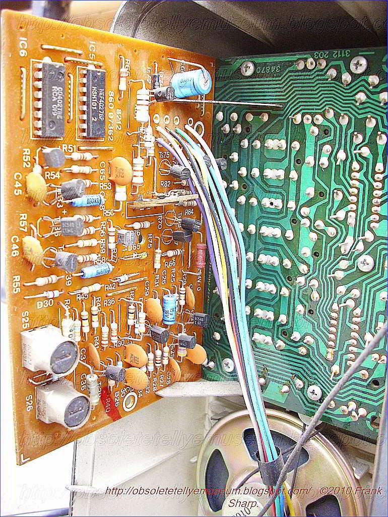

PHILIPS 12B912 /38C CHASSIS TX On a monocarrier are present all parts of the receiver inclusive the power supply with mains transformer.
On the left side up the tuning unit + remote control signal receiver based on cmos IC CD Series after models have implemented a Microcontroller TMS1100 type.
The Philips TX monochrome portable chassis has been in production for several years and large numbers have been sold in the Philips model ranges. several versions, with 12 and 14in. tubes, and with/without remote control. There have also been a number of modifications - most of these are of little significance from the servicing point of view, though it's worth noting that a simplified field generator stage is used in later production.
Power Supply Circuit:

 As
with any set, the power supply is the key to what goes on. The circuit
of the TX's power supply, which consists basically of a transformer -fed
mains bridge rectifier followed by a series regulator, is shown in Fig.
5. This is conventional though there are one or two points worth
noting. First, one of the diodes in the bridge rectifier circuit, D110,
also serves as the reverse polarity protection diode on battery
operation. Switch SK2 is part of the battery input socket. This can
cause problems, as we shall see. Secondly the error detector/amplifier
transistor TS112 is operated from the line output stage derived 26V
boost rail. This provides protection against excessive voltages in the
line output stage, since excessive boost voltage will cut off TS112 and
in turn TS111 and TS110. In the event of line output stage failure,
TS112, TS111 and TS110 will again be cut off. The result could be excess
voltage on the 10.8V line which will also be unstabilised, i.e. fed via
RHO only. This would damage the tube, whose heater is connected across
the 10.8V rail. To avoid this situation, diodes D115 and D116 conduct
when the line output stage is not working, thus reducing the voltage on
the 10.8V line. These diodes were not fitted in early production sets.
The fourth transistor TS113 provides the tuner with a stabilized 11.3V
supply. The tuning voltage is stabilized by a TAA550 in the usual way.
As
with any set, the power supply is the key to what goes on. The circuit
of the TX's power supply, which consists basically of a transformer -fed
mains bridge rectifier followed by a series regulator, is shown in Fig.
5. This is conventional though there are one or two points worth
noting. First, one of the diodes in the bridge rectifier circuit, D110,
also serves as the reverse polarity protection diode on battery
operation. Switch SK2 is part of the battery input socket. This can
cause problems, as we shall see. Secondly the error detector/amplifier
transistor TS112 is operated from the line output stage derived 26V
boost rail. This provides protection against excessive voltages in the
line output stage, since excessive boost voltage will cut off TS112 and
in turn TS111 and TS110. In the event of line output stage failure,
TS112, TS111 and TS110 will again be cut off. The result could be excess
voltage on the 10.8V line which will also be unstabilised, i.e. fed via
RHO only. This would damage the tube, whose heater is connected across
the 10.8V rail. To avoid this situation, diodes D115 and D116 conduct
when the line output stage is not working, thus reducing the voltage on
the 10.8V line. These diodes were not fitted in early production sets.
The fourth transistor TS113 provides the tuner with a stabilized 11.3V
supply. The tuning voltage is stabilized by a TAA550 in the usual way.Line Timebase:
The line generator circuit (Fig. 6) is rather unusual. The first transistor TS380 provides
the flywheel sync action: a line -frequency sawtooth is applied to its
emitter while the line sync pulses are applied to its base. Following
the flywheel sync filter, TS392 sets the voltage conditions in the line
hold control network. The oscillator itself consists of TS390 and TS391
which are connected in an emitter coupled astable multivibrator
configuration. The driver and output stages (Fig. 7) follow normal practice. D450
is the efficiency diode, D451 the boost diode, C451 the boost reservoir
capacitor and C450 the flyback tuning capacitor. The output stage
provides 9.5kV e.h.t. for the tube, a 350V supply for the tube's first
anode, a 95V supply for the video output stage and the tuning system,
and the 26V boost line.
The driver and output stages (Fig. 7) follow normal practice. D450
is the efficiency diode, D451 the boost diode, C451 the boost reservoir
capacitor and C450 the flyback tuning capacitor. The output stage
provides 9.5kV e.h.t. for the tube, a 350V supply for the tube's first
anode, a 95V supply for the video output stage and the tuning system,
and the 26V boost line.No Sound or Raster:
If there's no sound or raster, check the voltage at the emitter of TS110. If there's no voltage here, check the fuses - VL100 (on the mains transformer), VL110 and VL111. If VL100 or VL110 is open -circuit, check the bridge rectifier diodes D110/111/113/114 and the protection capacitors C116-9 for shorts and if necessary the mains transformer T110 for shorted turns. If VL111 is open -circuit, the 1.t. reservoir capacitor C112 could be leaky. Alternatively there could be a short-circuit in the line or sound output stage. Check the output transistor TS450, then D450, C450 and the scan coupling capacitor C455 in the line output stage. Check the smoothing capacitor C314 (47μF) and the output coupling capacitor C311 (100μF) in the audio output stage. If the fuses are o.k., check the voltage at the collector of TS110. If this is low at 2-8V, check TS110, TS111 and TS112 as necessary. If the voltage at the collector of TS110 is more than 8V, check the boost voltage - at pin 6 of the line output transformer. If the voltage here is less than 15V, check the line output transistor, check whether C455 is leaky, then check the line output transformer by substitution. If the voltage at pin 6 is in excess of 15V, check whether R451 is open -circuit, thus removing the supply to the line oscillator. In the event of R451 being open -circuit, check for shorts in the field generator circuit. If R451 is o.k., check the voltage at the base of the line driver transistor TS410. The reading should be about -0.1V. If this is present, check TS410 and TS450. If the reading is absent, check whether R401 is open -circuit, thus removing the supply to the line oscillator stage. Finally check TS390, TS391 and TS410 by replacement.
Normal Sound, No Raster:
For the sound normal, no raster condition, first check whether the tube's heater is alight. If not, check the continuity of the heater winding. Next remove the aerial plug. If there's insufficient brightness, check the a.g.c. amplifier transistor TS351 (BC548) by replacement. If there's still no brightness, turn the contrast to minimum, the brightness to maximum, and make voltage checks at the c.r.t. base. The cathode voltage (pin 2) should be 67V. If this is incorrect, check the video output transistor TS560 (BF422) and if necessary the field flyback blanking transistor TS565 (BC548C). If the voltage at pin 2 is correct, check the grid voltage (pin 5) which should be about 57V. If this voltage is missing, check whether the grid decoupling capacitor C572 (0.1μF) is short-circuit, then check whether the 95V supply is being developed across C452. If not, check R450 and D453 for being open -circuit. Next check the first anode voltage (pin 6) which should be 160V. If not, check R570 (820kOhm), R452 and D455. Finally check the e.h.t. circuit if necessary - from pin 8 of the line output transformer through the rectifier to the final anode of the c.r.t. Normal Sound, Weak or No Picture In the event of normal sound with a weak picture or no picture, check the voltage at the emitter of the video output transistor TS560. This should be 3.3V. If incorrect, check TS560; if correct, check the video driver transistor TS350 (BC558).
Field Collapse:
In the event of field collapse, check whether the field output stage feed resistor R529 (33n) is open -circuit. If so replace it and check the output transistors TS521/2 (BC338/BC328). Next check the field output stage midpoint voltage - 10.1V at the emitter of TS521. If this is incorrect, check the output transistors, the field driver transistor TS523 (BC548) and the preamplifier transistor TS520 (BC559B). If necessary che
 ck
the scan coupling capacitor C527 (100μF) and the earth return resistor
R527 (4.7Ohm), then suspect the field generator circuit. Check the
transistors TS505/TS509/TS515 and the values of resistors R515 (470kf1),
R517 (3901(n) and R516 (height control - 220kn). The original field
generator circuit is shown in Fig. 1. The charging capacitor C503
charges from the 26V rail via R503, R507 and the constant -current
transistor TS505. When the ramp at the emitter of TS505 reaches the
voltage at its base, set by R502/4, TS505 switches off. The positive
-going voltage at its collector then switches TS509 on, and in turn
TS515 to discharge C503.
ck
the scan coupling capacitor C527 (100μF) and the earth return resistor
R527 (4.7Ohm), then suspect the field generator circuit. Check the
transistors TS505/TS509/TS515 and the values of resistors R515 (470kf1),
R517 (3901(n) and R516 (height control - 220kn). The original field
generator circuit is shown in Fig. 1. The charging capacitor C503
charges from the 26V rail via R503, R507 and the constant -current
transistor TS505. When the ramp at the emitter of TS505 reaches the
voltage at its base, set by R502/4, TS505 switches off. The positive
-going voltage at its collector then switches TS509 on, and in turn
TS515 to discharge C503.
Loss of Line Sync:
In the event of loss of line sync, first remove the aerial input and check that the 1.t. line is correctly set for 10.8V. If the correct voltage cannot be obtained by adjusting R113, check TS110, TS111, TS112 and make sure that R114 is 3.9Ohm (in some sets it's 4.7MOhm). If the supplies are correct, check the voltage at the positive side of the a.g.c. smoothing capacitor C351 (47μF). With the aerial discon- nected the reading should be 4.3V. With the aerial connected a reading of 6-8V should be obtained. If the voltage conditions are incorrect, suspect the a.g.c. amplifier transistor TS351 (BC548). If necessary, try adjusting the line hold control R394 with the emitter of the flywheel sync transistor TS380 shorted to chassis and the aerial connected. If line lock cannot be obtained, replace the line oscillator transistors TS390 and TS391. If line lock can be obtained but the sync floats on removing the shorting link, suspect TS380 and TS392.
Miscellaneous Faults and Modifications:
Sound buzz with unstable picture, possibly intermittent: Suspect the battery socket - the switch can become tarnished. Replacement cures. Uncontrollable sound: Suspect the d.c. volume control R302 (4.710 or the TBA120AS intercarrier sound chip (IC310). Intermittent line collapse, with vertical line: Change C393 to 0.0015μF. Philips advise that the value of C393 in all sets bearing factory code HU on the chassis or serial plate is checked and changed to 0.0015μF if necessary. Bright vertical line at left-hand side: If a replacement line output transformer does not cure this, change C412 to 0.006814F and TS410 to a BC637 (note that the base connections differ). Distortion at low volume: Change R300 to 18kOhm, R311 to 56f1, R312 to 3.3kOhm/ and R315 to 120kOhm. Brightness range: Where the tube is type 12VCUP4, R576 should be 470kOhm Where the tube is type 12BJP4 it should be 820kOhm.
Power supply is realized with mains transformer and Linear transistorized power supply stabilizer, A DC power supply apparatus includes a rectifier circuit which rectifies an input commercial AC voltage. The rectifier output voltage is smoothed in a smoothing capacitor. Voltage stabilization is provided in the stabilizing circuits by the use of Zener diode circuits to provide biasing to control the collector-emitter paths of respective transistors.A linear regulator circuit according to an embodiment of the present invention has an input node receiving an unregulated voltage and an output node providing a regulated voltage. The linear regulator circuit includes a voltage regulator, a bias circuit, and a current control device.
In one embodiment, the current control device is implemented as an NPN bipolar junction transistor (BJT) having a collector electrode forming the input node of the linear regulator circuit, an emitter electrode coupled to the input of the voltage regulator, and a base electrode coupled to the second terminal of the bias circuit. A first capacitor may be coupled between the input and reference terminals of the voltage regulator and a second capacitor may be coupled between the output and reference terminals of the voltage regulator. The voltage regulator may be implemented as known to those skilled in the art, such as an LDO or non-LDO 3-terminal regulator or the like.
The bias circuit may include a bias device and a current source. The bias device has a first terminal coupled to the output terminal of the voltage regulator and a second terminal coupled to the control electrode of the current control device. The current source has an input coupled to the first current electrode of the current control device and an output coupled to the second terminal of the bias device. A capacitor may be coupled between the first and second terminals of the bias device.
In the bias device and current source embodiment, the bias device may be implemented as a Zener diode, one or more diodes coupled in series, at least one light emitting diode, or any other bias device which develops sufficient voltage while receiving current from the current source. The current source may be implemented with a PNP BJT having its collector electrode coupled to the second terminal of the bias device, at least one first resistor having a first end coupled to the emitter electrode of the PNP BJT and a second end, a Zener diode and a second resistor. The Zener diode has an anode coupled to the base electrode of the PNP BJT and a cathode coupled to the second end of the first resistor. The second resistor has a first end coupled to the anode of the Zener diode and a second end coupled to the reference terminal of the voltage regulator. A second Zener diode may be included having an anode coupled to the cathode of the first Zener diode and a cathode coupled to the first current electrode of the current control device.
 A circuit is disclosed for improving operation of a linear regulator, having an input terminal, an output terminal, and a reference terminal. The circuit includes an input node, a transistor, a bias circuit, and first and second capacitors. The transistor has a first current electrode coupled to the input node, a second current electrode for coupling to the input terminal of the linear regulator, and a control electrode. The bias circuit has a first terminal for coupling to the output terminal of the linear regulator and a second terminal coupled to the control electrode of the transistor. The first capacitor is for coupling between the input and reference terminals of the linear regulator, and the second capacitor is for coupling between the output and reference terminals of the linear regulator. The bias circuit develops a voltage sufficient to drive the control terminal of the transistor and to operate the linear regulator. The bias circuit may be a battery, a bias device and a current source, a floating power supply, a charge pump, or any combination thereof. The transistor may be implemented as a BJT or FET or any other suitable current controlled device.
 Power
Supply: The examples chosen are taken from manufacturers' circuit
diagrams and are usually simplified to emphasise the fundamental nature
of the circuit. For each example the particular transistor properties
that are exploited to achieve the desired performance are made clear. As
a rough and ready classification the circuits are arranged in order of
frequency: this part is devoted to circuits used at zero frequency,
field frequency and audio frequencies. Series Regulator Circuit Portable
television receivers are designed to operate from batteries (usually
12V car batteries) and from the a.c. mains. The receiver usually has an
11V supply line, and circuitry is required to ensure that the supply
line is at this voltage whether the power source is a battery or the
mains. The supply line also needs to have good regulation, i.e. a low
output resistance, to ensure that the voltage remains constant in spite
of variations in the mean current taken by some of the stages in the
receiver. Fig. 1 shows a typical circuit of the power -supply
arrangements. The mains transformer and bridge rectifier are designed to
deliver about 16V. The battery can be assumed to give just over 12V.
Both feed the regulator circuit Trl, Tr2, Tr3, which gives an 11V output
and can be regarded as a three -stage direct -coupled amplifier. The
first stage Tr 1 is required to give an output current proportional to
the difference between two voltages, one being a constant voltage
derived from the voltage reference diode D I (which is biased via R3
from the stabilised supply). The second voltage is obtained from a
preset potential divider connected across the output of the unit, and is
therefore a sample of the output voltage. In effect therefore Tr 1
compares the output voltage of the unit with a fixed voltage and gives
an output current proportional to the difference between them. Clearly a
field-effect transistor could do this, but the low input resistance of a
bipolar transistor is no disadvantage and it can give a current output
many times that of a field-effect transistor and is generally preferred
therefore. The output current of the first stage is amplified by the two
subsequent stages and then becomes the output current of the unit.
Clearly therefore Tr2 and Tr3 should be current amplifiers and they
normally take the form of emitter followers or common emitter stages
(which have the same current gain). By adjusting the preset control we
can alter the fraction of the output voltage' applied to the first stage
and can thus set the output voltage of the unit at any desired value
within a certain range. By making assumptions about the current gain of
the transistors we can calculate the degree of regulation obtainable.
For example, suppose the gain of Tr2 and Tr3 in cascade is 1,000, and
that the current output demanded from the unit changes by 0.1A (for
example due to the disconnection of part of the load). The corresponding
change in Tr l's collector current is 0.1mA and, if the standing
collector current of Tr 1 is 1mA, then its mutual conductance is
approximately 4OmA/V and the base voltage must change by 2.5mV to bring
about the required change in collector current. If the preset potential
divider feeds one half of the output voltage to Tr l's base, then the
change in output voltage must be 5mV. Thus an 0.1A change in output
current brings about only 5mV change in output voltage: this represents
an output resistance of only 0.0552.
Power
Supply: The examples chosen are taken from manufacturers' circuit
diagrams and are usually simplified to emphasise the fundamental nature
of the circuit. For each example the particular transistor properties
that are exploited to achieve the desired performance are made clear. As
a rough and ready classification the circuits are arranged in order of
frequency: this part is devoted to circuits used at zero frequency,
field frequency and audio frequencies. Series Regulator Circuit Portable
television receivers are designed to operate from batteries (usually
12V car batteries) and from the a.c. mains. The receiver usually has an
11V supply line, and circuitry is required to ensure that the supply
line is at this voltage whether the power source is a battery or the
mains. The supply line also needs to have good regulation, i.e. a low
output resistance, to ensure that the voltage remains constant in spite
of variations in the mean current taken by some of the stages in the
receiver. Fig. 1 shows a typical circuit of the power -supply
arrangements. The mains transformer and bridge rectifier are designed to
deliver about 16V. The battery can be assumed to give just over 12V.
Both feed the regulator circuit Trl, Tr2, Tr3, which gives an 11V output
and can be regarded as a three -stage direct -coupled amplifier. The
first stage Tr 1 is required to give an output current proportional to
the difference between two voltages, one being a constant voltage
derived from the voltage reference diode D I (which is biased via R3
from the stabilised supply). The second voltage is obtained from a
preset potential divider connected across the output of the unit, and is
therefore a sample of the output voltage. In effect therefore Tr 1
compares the output voltage of the unit with a fixed voltage and gives
an output current proportional to the difference between them. Clearly a
field-effect transistor could do this, but the low input resistance of a
bipolar transistor is no disadvantage and it can give a current output
many times that of a field-effect transistor and is generally preferred
therefore. The output current of the first stage is amplified by the two
subsequent stages and then becomes the output current of the unit.
Clearly therefore Tr2 and Tr3 should be current amplifiers and they
normally take the form of emitter followers or common emitter stages
(which have the same current gain). By adjusting the preset control we
can alter the fraction of the output voltage' applied to the first stage
and can thus set the output voltage of the unit at any desired value
within a certain range. By making assumptions about the current gain of
the transistors we can calculate the degree of regulation obtainable.
For example, suppose the gain of Tr2 and Tr3 in cascade is 1,000, and
that the current output demanded from the unit changes by 0.1A (for
example due to the disconnection of part of the load). The corresponding
change in Tr l's collector current is 0.1mA and, if the standing
collector current of Tr 1 is 1mA, then its mutual conductance is
approximately 4OmA/V and the base voltage must change by 2.5mV to bring
about the required change in collector current. If the preset potential
divider feeds one half of the output voltage to Tr l's base, then the
change in output voltage must be 5mV. Thus an 0.1A change in output
current brings about only 5mV change in output voltage: this represents
an output resistance of only 0.0552.TDA2540 IF AMPLIFIER WITH DEMODULATOR AND AFC
DESCRIPTION
The TDA2540 and 2541 are IF amplifier and A.M.
demodulator circuits for colour and black and white
televisionreceiversusingPNPorNPNtuners. They
are intended for reception of negative or positive
modulation CCIR standard.
They incorporate the following functions : .Gain controlled amplifier .Synchronous demodulator .White spot inverter .Video preamplifier with noise protection .Switchable AFC .AGC with noise gating .Tuner AGC output (NPN tuner for 2540)-(PNP
tuner for 2541) .VCR switch for video output inhibition (VCR
play back)
.SUPPLYVOLTAGE : 12V TYP
.SUPPLYCURRENT : 50mATYP
.I.F. INPUT VOLTAGE SENSITIVITY ATF = 38.9MHz : 85mVRMS TYP
.VIDEO OUTPUT VOLTAGE (white at 10% oftop synchro) : 2.7VPP TYP
.I.F. VOLTAGE GAIN CONTROL RANGE :
64dB TYP .SIGNAL TO NOISE RATIO AT VI = 10mV :
58dB TYP .A.F.C. OUTPUT VOLTAGE SWING FOR
Df = 100kHz : 10V TYP
PHILIPS 12B912 /38C CHASSIS TX TELEVISION DIAGRAM AND DEFLECTION CIRCUIT:
A unidirectional conductive device is coupled from a base terminal to a collector terminal of a horizontal deflection output transistor in a television receiver and poled in a direction to prevent the transistor from saturating when it is driven into its conductive state during a portion of each deflection cycle. Biasing means is coupled to the diode to preselect the desired operating voltage of the transistor during its conduction period.
1. In a television receiver, a deflection circuit comprising: 2. A circuit as defined in claim 1 wherein said transformer is an auto-transformer and said second terminal is intermediate said first and 3. In a television receiver, a deflection circuit comprising:
Description:
The present invention relates to transistorized deflection circuits utilized in television receivers.
In present day transistor deflection circuits, for example, those used in the horizontal output stage of a television receiver; the output transistor is normally operated in a switching mode, that is, the transistor is driven into saturation during a trace interval of each deflection cycle and driven out of conduction during the retrace portion of each deflection cycle. By operating the transistor in its saturation region, average power losses are minimized. With saturated operation, however, the accumulation of minority carriers in the base region will effect a continuation in the flow of collector current after the trace interval during the initial portion of the retrace interval while the transistor is being driven into its non-conducting state. In addition to causing this undesirable delay time in turning off the transistor, losses occurring during this period may be localized in small areas commonly referred to as "hot spots." These losses are characterized in being regenerative and tend to cause second breakdown of the device. This effect is explained in greater detail in a paper authored by the present inventor and entitled "Thermal Regeneration in Power Dissipating Elements" which appeared in "The Electronic Engineer" publication in the January 1967 issue. Although operating the horizontal output transistor in its saturated region may reduce the average power dissipated in this device during its conduction interval, it increases the possibility of second breakdown during the turn-off time. With the advent of high voltage (1,500 volts) transistors, it is possible to develop the necessary output energy utilizing one of these transistors which can be operated in a non-saturated mode. The circuit of the present invention insures that the deflection output transistor will not be driven into saturation.
 Certain low power transistor switching circuits, such as employed in computer applications, have utilized diodes in conjunction with resistive biasing means coupled between the base and collector terminals to prevent the transistor from saturating and thereby increase the maximum switching frequency of the circuit by reducing the turn-off time of the device.
In the solid state deflection art, however, it is desirable to reduce the turn-off time of the device not to increase the frequency of operation of the circuit, but rather to prevent second breakdown of the device as the relatively large inductive voltage pulse appears during the initial portion of the flyback interval, when current flowing through the deflection winding is interrupted to initiate the retrace portion of each deflection cycle.
The non-saturated operation of the deflection output transistor is achieved in circuits embodying the present invention by automatically holding the collector voltage above the saturation level by shunting excess base drive from the base to emitter junction into the collector circuit. Prior transistor deflection systems employ only the saturated operation of the deflection output device.
Circuits embodying the present invention include a deflection output transistor having a diode coupled between its base and collector terminals and poled to prevent the transistor from being driven into saturation during its conduction period of each deflection cycle.
The invention can be more fully understood by referring to the drawings together with the description below and the accompanying claims.
In the drawings:
FIG. 1 illustrates in block and schematic diagram form, a television receiver including a solid state deflection output stage embodying the present invention;
FIG. 2a is a waveform diagram of the voltage present at the collector terminal 55c of transistor 55 in FIG. 1;
FIG. 2b shows the drive current to terminal A in FIG. 1;
FIG. 2c is a waveform diagram of the current in diode 56 in FIG. 1;
FIG. 2d is a waveform diagram of the base current flowing in transistor 55 of FIG. 1;
FIG. 3 is a schematic diagram of an alternative embodiment of the present invention;
FIG. 4a is a waveform diagram of the voltage appearing at the terminal 366 in FIG. 3;
FIG. 4b is a waveform diagram of the drive current to terminal A in FIG. 3;
FIG. 4c is a waveform diagram of the current in diode 356 in FIG. 3; and
FIG. 4d is a waveform diagram of the base drive current to transistor 355 in FIG. 3.
Referring specifically to FIG. 1,an antenna 10 receives television signals and couples these signals to a tuner 12 which selects the desired radio frequency signals of a predetermined broadcast channel, amplifies these signals, and converts the amplified radio frequency signals to a lower intermediate frequency (I.F.). The tuner 12 is coupled to an I.F. amplifier 14 which amplifies the intermediate frequency signals. The I.F. amplifier 14 is coupled to a video detector 16 which derives video information from the I.F. signals. The video detector 16 is coupled to a video driver stage 18 which amplifies the video signals. The video driver stage 18 is coupled to a video output stage 20, an automatic gain control stage 25 and a synchronizing separator stage 42. An output signal from video driver stage 18 may also be coupled to a sound channel (not shown) to reproduce the audio portion of the transmitted television program. The video output stage 20 couples amplified video information to a control element, such as a cathode 28, of a kinescope 30.
The automatic gain control stage 25 operates in a conventional manner to provide gain control signals which are applied to a radio frequency amplifier included in tuner 12 and to the I.F. amplifier 14. Sync separator 42 separates the synchronization information from the video information and also separates the horizontal synchronizing information for the vertical synchronizing information. The vertical synchronizing pulses derived from sync separator 42 are applied to the vertical deflection system 44 which provides the required deflection current to a vertical deflection winding 43 associated with kinescope 30 by means of the interconnection Y--Y. The horizontal synchronizing pulses from sync separator 42 are applied to an automatic frequency control detector 45 which serves to synchronize a horizontal oscillator 46 with the horizontal synchronizing pulses. The horizontal oscillator stage 46 is coupled to a horizontal driver stage 48 which develops the required drive signal and may be coupled by means of an output transformer in stage 48 (not shown) to a transistorized horizontal output stage 50. The transformer secondary, coupled to terminal A, provides a direct current path for the drive current.
The horizontal output stage 50 includes an output transistor 55 having a base, a collector and an emitter terminal 55b, 55c and 55e, respectively. A resistor 52 and a capacitor 53 are coupled in parallel between the horizontal driver stage 48 and the base terminal 55b of transistor 55.
The output stage includes a unidirectional conductive device such as a diode 56 coupled between the base and collector terminals 55b and 55c of transistor 55. Stage 50 also includes a damper diode 57 coupled across transistor 55, a retrace capacitor 58 coupled across transistor 55 and the series combination of a horizontal deflection winding 59 and an S-shaping capacitor 60 also coupled across transistor 55. Output stage 50 also includes a flyback transformer 61 with a primary winding 61p coupled from a source of operating potential (B+) to the collector terminal 55c of transistor 55. A secondary winding 61s on transformer 61 develops high voltage pulses which are coupled to a high voltage rectifier 63 to provide the ultor voltage for application to a terminal 32 on kinescope 30. Flyback transformer 61 may also include additional windings (not shown) for providing, for example, keying pulses to the AGC stage 25.
The output stage 50 in FIG. 1 is a conventional shunt fed trace driven circuit with the exception of the diode 56 and the bias network including resistor 52 and capacitor 53. Beginning at the center of the trace interval of the deflection cycle, the yoke current is zero and capacitor 60 has a maximum charge. The drive signal applied to the base terminal 55b of transistor 55 turns this device on, thereby completing the conduction path for yoke current which includes capacitor 60, yoke 59 and the collector to emitter current path through transistor 55. During this portion of scan the yoke current is supplied by the charge on capacitor 60 and increases to a maximum value in one direction at which time scan retrace is initiated by driving transistor 55 out of conduction by applying an appropriate signal from the driver stage 48 to the base 55b of transistor 55. During the latter portion of the trace interval when the magnitude of the yoke current is increasing, the output transistor of prior circuits is normally driven into saturation and is in this conduction state at the instant retrace is initiated. During the first portion of retrace, the yoke current is at a maximum and resonates with the retrace capacitor 58 by charging capacitor 58 in a polarity to reverse bias the damper diode 57. As the yoke current decreases to zero, capacitor 58 has a maximum charge impressed upon it; and during the second portion of retrace, the capacitor (58) drives current through the yoke in a reverse direction until it is discharged and the voltage across it reverses sufficiently to forward bias damper diode 57. Diode 57 then conducts during this first portion of trace to complete the current path for yoke current which is, at this instant, at a maximum value in a direction in yoke 59 to charge capacitor 60 and is increasing toward zero. At the mid-point of trace the yoke current has reached zero and the cycle is completed by driving transistor 55 into conduction once again.
Turning now to the operation of the circuitry of FIG. 1 including the present invention, reference is made to the waveform diagrams of FIG. 2. The initial portion of trace is represented in FIG. 2 by the time period between t 0 and t 1 in the figure. It is recalled that during this period damper diode 57 is conducting. The voltage at collector terminal 55c of transistor 55 is represented by the voltage waveform (V c ) in FIG. 2a and is equal to the forward voltage drop across diode 57 which is of the order of -0.7 volts. At some non-critical time before t 1 , the horizontal driver 48 provides a drive current (I A ), as is shown in FIG. 2b. This current flows through diode 56 as is illustrated in FIG. 2c, since the diode is forward biased. [The cathode of diode 56 is at the same voltage as collector terminal 55c (-0.07 volts) and the drive current produces a positive voltage at point A which is at the anode of diode 56.] As time t 1 (the center of trace) is reached, damper diode 57 turns off allowing the collector voltage on transistor 55 to increase as shown in FIG. 2a. At the same time, a portion of the drive current flowing into terminal A is conducted by the now forward biased base to emitter junction of transistor 55 as is illustrated by the waveform of FIG. 2d. Transistor 55 is now conducting the increasing yoke current during the latter portion of scan represented by the period from t 1 to t 2 in FIG. 2. As the magnitude of the yoke current increases during the t 1 to t 2 interval, the base current in transistor 55 increases as shown in FIG. 2d. Diode 56 conducts as illustrated in FIG. 2c to shunt the remaining portion of the applied drive current at terminal A. It is noted that the sum of the currents shown in FIGS. 2c and 2d will equal the current shown in FIG. 2b. T he values of resistor 52 and capacitor 53 can be selected to hold the transistor collector voltage at a preselected value sufficient to prevent saturation of the transistor 55. If, for example, the voltage across capacitor 53 is 5.3 volts, the voltage at terminal A with respect to ground will be approximately 6 volts (5.3 volts plus the forward voltage drop across the base-emitter junction of transistor 55). The collector voltage will then be approximately equal to the voltage at terminal A less the forward voltage drop across diode 56. It is desirable to choose values of resistor 52 and capacitor 53 to operate transistor 55 near but not into the saturation region of conduction during the latter portion of each trace interval.
At time t 2 retrace is initiated by applying a relatively large negative drive signal as shown in FIG. 2b to the base terminal of transistor 55. During the retrace interval (t 2 to t 0 in FIG. 2), the collector voltage increases in a typical manner as illustrated in FIG. 2a. At time t 0 the cycle is again repeated.
The circuit modification illustrated in FIG. 3 is another embodiment of the invention which reduces the change in voltage applied to the yoke 59 of FIG. 1 at time t 1 . As shown in FIG. 2a, when diode 57 turns off and transistor 55 conducts, the voltage at the collector terminal 55c of transistor 55 changes by as much, for example, as 6 volts. This voltage change, which is coupled to the yoke 59, will vary the rate of change of yoke current during the center of trace and may, in certain circuits, cause an undesirable non-linearity in the scanning rate. As FIG. 4a illustrates, the circuit of FIG. 3 reduces this change in voltage at the mid-point of trace (t 1 ).
Referring to FIG. 3, the circuit elements which correspond to those of FIG. 1 are prefaced by the numeral 3. In explaining FIG. 3, it is helpful to refer to the waveform diagrams of FIG. 4. Transformer 364 in FIG. 3 is a tightly coupled auto-transformer wherein the tap point 365 may be, for example, at the 5 percent point on the transformer. That is, the segment between terminals 365 and 366 contain 5 percent of the total number of windings on transformer 364. Transformer 364 may also include a secondary winding such as the high voltage winding which is not shown in the figure. In operation, as drive current is applied at sometime prior to t 1 as is shown in FIG. 4b, damper diode 357 is conducting and the voltage at terminal 366 is therefore at approximately -0.7 volts. Drive current flowing into terminal A as represented in FIG. 4b will be conducted by diode 356 during this interval as indicated by the diode current waveform in FIG. 4c. At the middle portion of trace (t 1 ), the damper diode turns off and voltage at terminal 366 is thereby allowed to go slightly positive (less than 0.7 volts). The collector voltage of transistor 355 is held at a value of approximately 5 volts (assuming, for example, the B+ voltage is equal to 100 volts and the collector is coupled to the tap 365 on transformer 364 at a 5 percent point). At this instant, the base to emitter junction will be forward biased and transistor 355 conducts. It is seen that the anode voltage of diode 356 is at approximately +0.7 volts and its cathode which is coupled to terminal 366 is at a less positive voltage. Diode 356 begins to conduct during the latter portion of trace as illustrated by the current waveform diagram shown in FIG. 4c.
During the latter portion of trace, the transistor tends to saturate and the collector voltage at terminal 355c tends to decrease. As this occurs, more current will flow from the B+ terminal through the upper portion of transformer 364. Due to the relatively tight coupling of the segments of transformer 364, terminal 366 experiences a decrease in voltage which controls the forward bias applied to diode 356 to shunt sufficient drive current to hold the transistor 355 out of saturation. The collector voltage of transistor 355 is thus held at some preselected value depending on the location of tap point 365 on transformer 364. Since transformer 364 is utilized, terminal 366 will remain at a low voltage during the latter portion of trace as shown in FIG. 4a, and diode 356 will be forward biased during the application of a positive drive signal to terminal A. As before, the base drive current will increase and diode 356 conduction will decrease generally as shown in FIGS. 4c and 4d during the latter portion of trace. At time t 2 in FIG. 4, a negative drive pulse is applied to the circuit which initiates the retrace interval of the deflection cycle.
Although the specific embodiments of the invention are illustrated in the horizontal deflection output stage of a black and white television receiver, the invention has equal applicability to other deflection systems and may be utilized in a color television receiver.
In present day transistor deflection circuits, for example, those used in the horizontal output stage of a television receiver; the output transistor is normally operated in a switching mode, that is, the transistor is driven into saturation during a trace interval of each deflection cycle and driven out of conduction during the retrace portion of each deflection c
ycle. By operating the transistor in its saturation region, average power losses are minimized. With saturated operation, however, the accumulation of minority carriers in the base region will effect a continuation in the flow of collector current after the trace interval during the initial portion of the retrace interval while the transistor is being driven into its non-conducting state. In addition to causing this undesirable delay time in turning off the transistor, losses occurring during this period may be localized in small areas commonly referred to as "hot spots." These losses are characterized in being regenerative and tend to cause second breakdown of the device. This effect is explained in greater detail in a paper authored by the present inventor and entitled "Thermal Regeneration in Power Dissipating Elements" which appeared in "The Electronic Engineer" publication in the January 1967 issue. Although operating the horizontal output transistor in its saturated region may reduce the average power dissipated in this device during its conduction interval, it increases the possibility of second breakdown during the turn-off time. With the advent of high voltage (1,500 volts) transistors, it is possible to develop the necessary output energy utilizing one of these transistors which can be operated in a non-saturated mode. The circuit of the present invention insures that the deflection output transistor will not be driven into saturation. Certain low power transistor switching circuits, such as employed in computer applications, have utilized diodes in conjunction with resistive biasing means coupled between the base and collector terminals to prevent the transistor from saturating and thereby increase the maximum switching frequency of the circuit by reducing the turn-off time of the device.
In the solid state deflection art, however, it is desirable to reduce the turn-off time of the device not to increase the frequency of operation of the circuit, but rather to prevent second breakdown of the device as the relatively large inductive voltage pulse appears during the initial portion of the flyback interval, when current flowing through the deflection winding is interrupted to initiate the retrace portion of each deflection cycle.
The non-saturated operation of the deflection output transistor is achieved in circuits embodying the present invention by automatically holding the collector voltage above the saturation level by shunting excess base drive from the base to emitter junction into the collector circuit. Prior transistor deflection systems employ only the saturated operation of the deflection output device.
Circuits embodying the present invention include a deflection output transistor having a diode coupled between its base and collector terminals and poled to prevent the transistor from being driven into saturation during its conduction period of each deflection cycle.
The invention can be more fully understood by referring to the drawings together with the description below and the accompanying claims.
In the drawings:
FIG. 1 illustrates in block and schematic diagram form, a television receiver including a solid state deflection output stage embodying the present invention;
FIG. 2a is a waveform diagram of the voltage present at the collector terminal 55c of transistor 55 in FIG. 1;
FIG. 2b shows the drive current to terminal A in FIG. 1;
FIG. 2c is a waveform diagram of the current in diode 56 in FIG. 1;
FIG. 2d is a waveform diagram of the base current flowing in transistor 55 of FIG. 1;
FIG. 3 is a schematic diagram of an alternative embodiment of the present invention;
FIG. 4a is a waveform diagram of the voltage appearing at the terminal 366 in FIG. 3;
FIG. 4b is a waveform diagram of the drive current to terminal A in FIG. 3;
FIG. 4c is a waveform diagram of the current in diode 356 in FIG. 3; and
FIG. 4d is a waveform diagram of the base drive current to transistor 355 in FIG. 3.
Referring specifically to FIG. 1,
an antenna 10 receives television signals and couples these signals to a tuner 12 which selects the desired radio frequency signals of a predetermined broadcast channel, amplifies these signals, and converts the amplified radio frequency signals to a lower intermediate frequency (I.F.). The tuner 12 is coupled to an I.F. amplifier 14 which amplifies the intermediate frequency signals. The I.F. amplifier 14 is coupled to a video detector 16 which derives video information from the I.F. signals. The video detector 16 is coupled to a video driver stage 18 which amplifies the video signals. The video driver stage 18 is coupled to a video output stage 20, an automatic gain control stage 25 and a synchronizing separator stage 42. An output signal from video driver stage 18 may also be coupled to a sound channel (not shown) to reproduce the audio portion of the transmitted television program. The video output stage 20 couples amplified video information to a control element, such as a cathode 28, of a kinescope 30.The automatic gain control stage 25 operates in a conventional manner to provide gain control signals which are applied to a radio frequency amplifier included in tuner 12 and to the I.F. amplifier 14. Sync separator 42 separates the synchronization information from the video information and also separates the horizontal synchronizing information for the vertical synchronizing information. The vertical synchronizing pulses derived from sync separator 42 are applied to the vertical deflection system 44 which provides the required deflection current to a vertical deflection winding 43 associated with kinescope 30 by means of the interconnection Y--Y. The horizontal synchronizing pulses from sync separator 42 are applied to an automatic frequency control detector 45 which serves to synchronize a horizontal oscillator 46 with the horizontal synchronizing pulses. The horizontal oscillator stage 46 is coupled to a horizontal driver stage 48 which develops the required drive signal and may be coupled by means of an output transformer in stage 48 (not shown) to a transistorized horizontal output stage 50. The transformer secondary, coupled to terminal A, provides a direct current path for the drive current.
The horizontal output stage 50 includes an output transistor 55 having a b
ase, a collector and an emitter terminal 55b, 55c and 55e, respectively. A resistor 52 and a capacitor 53 are coupled in parallel between the horizontal driver stage 48 and the base terminal 55b of transistor 55.The output stage includes a unidirectional conductive device such as a diode 56 coupled between the base and collector terminals 55b and 55c of transistor 55. Stage 50 also includes a damper diode 57 coupled across transistor 55, a retrace capacitor 58 coupled across transistor 55 and the series combination of a horizontal deflection winding 59 and an S-shaping capacitor 60 also coupled across transistor 55. Output stage 50 also includes a flyback transformer 61 with a primary winding 61p coupled from a source of operating potential (B+) to the collector terminal 55c of transistor 55. A secondary winding 61s on transformer 61 develops high voltage pulses which are coupled to a high voltage rectifier 63 to provide the ultor voltage for application to a terminal 32 on kinescope 30. Flyback transformer 61 may also include additional windings (not shown) for providing, for example, keying pulses to the AGC stage 25.
The output stage 50 in FIG. 1 is a conventional shunt fed trace driven circuit with the exception of the diode 56 and the bias network including resistor 52 and capacitor 53. Beginning at the center of the trace interval of the deflection cycle, the yoke current is zero and capacitor 60 has a maximum charge. The drive signal applied to the base terminal 55b of transistor 55 turns this device on, thereby completing the conduction path for yoke current which includes capacitor 60, yoke 59 and the collector to emitter current path through transistor 55. During this portion of scan the yoke current is supplied by the charge on capacitor 60 and increases to a maximum value in one direction at which time scan retrace is initiated by driving transistor 55 out of conduction by applying an appropriate signal from the driver stage 48 to the base 55b of transistor 55. During the latter portion of the trace interval when the magnitude of the yoke current is increasing, the output transistor of prior circuits is normally driven into saturation and is in this conduction state at the instant retrace is initiated. During the first portion of retrace, the yoke current is at a maximum and resonates with the retrace capacitor 58 by charging capacitor 58 in a polarity to reverse bias the damper diode 57. As the yoke current decreases to zero, capacitor 58 has a maximum charge impressed upon it; and during the second portion of retrace, the capacitor (58) drives current through the yoke in a reverse direction until it is discharged and the voltage across it reverses sufficiently to forward bias damper diode 57. Diode 57 then conducts during this first portion of trace to complete the current path for yoke current which is, at this instant, at a maximum value in a direction in yoke 59 to charge capacitor 60 and is increasing toward zero. At the mid-point of trace the yoke current has reached zero and the cycle is completed by driving transistor 55 into conduction once again.
Turning now to the operation of the circuitry of FIG. 1 including the present invention, reference is made to the waveform diagrams of FIG. 2. The initial portion of trace is represented in FIG. 2 by the time period between t 0 and t 1 in the figure. It is recalled that during this period damper diode 57 is conducting. The voltage at collector terminal 55c of transistor 55 is represented by the voltage waveform (V c ) in FIG. 2a and is equal to the forward voltage drop across diode 57 which is of the order of -0.7 volts. At some non-critical time before t 1 , the horizontal driver 48 provides a drive current (I A ), as is shown in FIG. 2b. This current flows through diode 56 as is illustrated in FIG. 2c, since the diode is forward biased. [The cathode of diode 56 is at the same voltage as collector terminal 55c (-0.07 volts) and the drive current produces a positive voltage at point A which is at the anode of diode 56.] As time t 1 (the center of trace) is reached, damper diode 57 turns off allowing the collector voltage on transistor 55 to increase as shown in FIG. 2a. At the same time, a portion of the drive current flowing into terminal A is conducted by the now forward biased base to emitter junction of transistor 55 as is illustrated by the waveform of FIG. 2d. Transistor 55 is now conducting the increasing yoke current during the latter portion of scan represented by the period from t 1 to t 2 in FIG. 2. As the magnitude of the yoke current increases during the t 1 to t 2 interval, the base current in transistor 55 increases as shown in FIG. 2d. Diode 56 conducts as illustrated in FIG. 2c to shunt the remaining portion of the applied drive current at terminal A. It is noted that the sum of the currents shown in FIGS. 2c and 2d will equal the current shown in FIG. 2b. T
 he values of resistor 52 and capacitor 53 can be selected to hold the transistor collector voltage at a preselected value sufficient to prevent saturation of the transistor 55. If, for example, the voltage across capacitor 53 is 5.3 volts, the voltage at terminal A with respect to ground will be approximately 6 volts (5.3 volts plus the forward voltage drop across the base-emitter junction of transistor 55). The collector voltage will then be approximately equal to the voltage at terminal A less the forward voltage drop across diode 56. It is desirable to choose values of resistor 52 and capacitor 53 to operate transistor 55 near but not into the saturation region of conduction during the latter portion of each trace interval.
At time t 2 retrace is initiated by applying a relatively large negative drive signal as shown in FIG. 2b to the base terminal of transistor 55. During the retrace interval (t 2 to t 0 in FIG. 2), the collector voltage increases in a typical manner as illustrated in FIG. 2a. At time t 0 the cycle is again repeated.
The circuit modification illustrated in FIG. 3 is another embodiment of the invention which reduces the change in voltage applied to the yoke 59 of FIG. 1 at time t 1 . As shown in FIG. 2a, when diode 57 turns off and transistor 55 conducts, the voltage at the collector terminal 55c of transistor 55 changes by as much, for example, as 6 volts. This voltage change, which is coupled to the yoke 59, will vary the rate of change of yoke current during the center of trace and may, in certain circuits, cause an undesirable non-linearity in the scanning rate. As FIG. 4a illustrates, the circuit of FIG. 3 reduces this change in voltage at the mid-point of trace (t 1 ).
Referring to FIG. 3, the circuit elements which correspond to those of FIG. 1 are prefaced by the numeral 3. In explaining FIG. 3, it is helpful to refer to the waveform diagrams of FIG. 4. Transformer 364 in FIG. 3 is a tightly coupled auto-transformer wherein the tap point 365 may be, for example, at the 5 percent point on the transformer. That is, the segment between terminals 365 and 366 contain 5 percent of the total number of windings on transformer 364. Transformer 364 may also include a secondary winding such as the high voltage winding which is not shown in the figure. In operation, as drive current is applied at sometime prior to t 1 as is shown in FIG. 4b, damper diode 357 is conducting and the voltage at terminal 366 is therefore at approximately -0.7 volts. Drive current flowing into terminal A as represented in FIG. 4b will be conducted by diode 356 during this interval as indicated by the diode current waveform in FIG. 4c. At the middle portion of trace (t 1 ), the damper diode turns off and voltage at terminal 366 is thereby allowed to go slightly positive (less than 0.7 volts). The collector voltage of transistor 355 is held at a value of approximately 5 volts (assuming, for example, the B+ voltage is equal to 100 volts and the collector is coupled to the tap 365 on transformer 3
64 at a 5 percent point). At this instant, the base to emitter junction will be forward biased and transistor 355 conducts. It is seen that the anode voltage of diode 356 is at approximately +0.7 volts and its cathode which is coupled to terminal 366 is at a less positive voltage. Diode 356 begins to conduct during the latter portion of trace as illustrated by the current waveform diagram shown in FIG. 4c.During the latter portion of trace, the transistor tends to saturate and the collector voltage at terminal 355c tends to decrease. As this occurs, more current will flow from the B+ terminal through the upper portion of transformer 364. Due to the relatively tight coupling of the segments of transformer 364, terminal 366 experiences a decrease in voltage which controls the forward bias applied to diode 356 to shunt sufficient drive current to hold the transistor 355 out of saturation. The collector voltage of transistor 355 is thus held at some preselected value depending on the location of tap point 365 on transformer 364. Since transformer 364 is utilized, terminal 366 wil
l remain at a low voltage during the latter portion of trace as shown in FIG. 4a, and diode 356 will be forward biased during the application of a positive drive signal to terminal A. As before, the base drive current will increase and diode 356 conduction will decrease generally as shown in FIGS. 4c and 4d during the latter portion of trace. At time t 2 in FIG. 4, a negative drive pulse is applied to the circuit which initiates the retrace interval of the deflection cycle.Although the specific embodiments of the invention are illustrated in the horizontal deflection output stage of a black and white television receiver, the invention has equal applicability to other deflection systems and may be utilized in a color television receiver.
No comments:
Post a Comment
The most important thing to remember about the Comment Rules is this:
The determination of whether any comment is in compliance is at the sole discretion of this blog’s owner.
Comments on this blog may be blocked or deleted at any time.
Fair people are getting fair reply. Spam and useless crap and filthy comments / scrapers / observations goes all directly to My Private HELL without even appearing in public !!!
The fact that a comment is permitted in no way constitutes an endorsement of any view expressed, fact alleged, or link provided in that comment by the administrator of this site.
This means that there may be a delay between the submission and the eventual appearance of your comment.
Requiring blog comments to obey well-defined rules does not infringe on the free speech of commenters.
Resisting the tide of post-modernity may be difficult, but I will attempt it anyway.
Your choice.........Live or DIE.
That indeed is where your liberty lies.
Note: Only a member of this blog may post a comment.