


-
The PHILIPS CHASSIS KT4 is the "small brother" of the PHILIPS K40 but not isolated from mains and without AV SCART SOCKET, it's basically a basic K40 but with further diversity from K40.
WAS specifically designed for small sets like the 20" PHILIPS 20CT4426 /08Z SEGANTINI here shown.


- Deflection Board on the right called large signal board. Line deflection output (BU508A) + EHT, E/W
Correction, FRAME Deflection Output with IC TDA3650 (PHILIPS)
- Signal processing board + Tuning control drive TRD (Tuning Remote Digital)
Chrominance + Luminance with TDA3561A, Synchronization With TDA3576B.
PHILIPS TDA3576B SYNC COMBINATION WITH TRANSMITTER IDENTIFICATION
AND VERTICAL 625 DIVIDER SYSTEM.
GENERAL DESCRIPTION
The TDA3576B is a monolithic integrated circuit for use in colour television receivers. The circuit is
optimized for a horizontal and vertical frequency ratio of 625.
Features
• Horizontal sync separator (including noise inverter) with sliding bias such that the sync pulse is
always sliced between top sync level and blanking level
• Phase detector which compares the horizontal sync pulse with the oscillator voltage; this phase
detector is gated
• Phase detector which compares the horizontal flyback pulse with the oscillator voltage
• Horizontal oscillator (31,25 kHz)
• Time constant switching of the first control loop (short time constant during catching and reception
of VCR signals)
• Burst key pulse generator (sandcastle pulse with three levels)
• Very stable automatic vertical synchronization due to the 625 divider system, without delay after
channel change
• Vertical sync pulse separator
• Three voltage level sensor on coincidence detector circuit output
• Video transmitter identification circuit for sound muting and search tuning systems
• Inhibit of vertical sync pulse when no video transmitter is detected.
FUNCTIONAL DESCRIPTION
The video input voltage to drive the sync separator must have negative-going sync, which can be
obtained from synchronous demodulators such as TDA2540 and TDA2541.
The slicing level of the sync separator is determined by the value of the resistor between pins 6 and 7. A
4, 7 kr2 resistor provides a slicing level midway between the top sync level and the blanking level. Thus
the slicing level is independent of the amplitude of the sync pulse input at pin 5.
The nominal top sync level at pin 5 is 3 V, and the amplitude selective noise inverter is activated at
0,7 V.
To
obtain good stability the circuit contains three control loops. In the
first loop the phase of the horizontal sync pulse is compared with a
reference output pulse from the horizontal oscillator. In the second
loop the phase of the flyback pulse is compared with the same reference
output pulse. The first loop is designed for good noise immunity and the
second loop has a fast time constant to compensate quickly for storage
variations of the output stage. The second loop also generates a gating
signal of about 5,5 μs for use in the transmitter identification
circuit. The third control loop generates a second gating signal which
is used in the first phase detector. The pulse width is typically 14 μs.
For a short catching time the output current of the first phase
detector is not gated but is increased by 5 times during catching. This
is caused by the voltage of the coincidence detector at pin 9. For VCR
playback conditions the first control loop must be forced to a fast time
constant, this is achieved by applying an external voltage of~ 2,7 V to
pin 9.
The free running output frequency of the horizontal
oscillator is 31,25 kHz. The vertical frequency output is obtained by
dividing this double horizontal frequency by 625. The double horizontal
fre- quency is fed via a binary divider to provide the normal 15,625 kHz
horizontal output to pin 11. The sandcastle pulse is generated at pin 2
and has three levels. The burst key pulse is of short duration,
typically 4 μs, with an amplitude of 10 Vandis the highest level. The
second level has a pulse duration equal to the horizontal flyback pulse
with an amplitude of 4,5 Vandis used for horizontal blanking. The third
level, amplitude 2,5 V, is used for vertical blanking and has a pulse
duration of 1,34 ms. The last pulse is internal Iv generated by the
divider circuit and is only available when a standard video input signal
is received. An external vertical blanking pulse can be added to this
pin via a suitable series resistor. This pulse will be automatically
clamped to 2,5 V.
The automatic vertical sync block contains the following:
• 625 divider
• In/out-sync detector
• Direct/indirect sync switch
• Identification circuit
It
is fed by a signal obtained by integration of the composite video
signal and an internally generated, clipped video signal. The vertical
sync pulse is sliced out of this integrated signal by an automatically
biased clipper. The video part of the signal helps to build up a
vertical sync when heavy negative-going reflections (mountains) distort
the video signal. The in/out sync-detector considers a signal
out-of-sync when fourteen or more successive incoming vertical sync
pulses are not in phase with a reference signal from the 625 divider.
Therefore a distorted vertical sync signal needs only one
out-of-fourteen pulses to be in phase to keep the system in sync. When
the fifteenth successive out-of-sync pulse is detected, the
direct/indirect sync switch is activated to feed the vertical sync
signal directly out of the block at pin 3 (direct sync vertical output).
At the same time the 625 divider is reset by one of the sync pulses.
After the reset pulse, if the 7th sliced vertical sync pulse coincides
with a 625 divider window, the sync output pulse is presenteu again by
the divider system and switch-over to indirect mode occurs. In the
direct mode, every 7th non-coinciding sliced vertical sync pulse will
reset the counter. A non- standard video signal will result in
continuous reset pulses and the direct/indirect switch will remain in
the direct position.
To avoid delay in vertical synchronization, caused by waiting time of the divider circuit after channel
change or an unsynchronized camera change in the studio, information is fed from the horizontal
coincidence detector to the automatic switch for the vertical sync pulse. The loss of horizontal
synchronization sets the automatic switch to direct vertical sync.
When an external voltage between 2,7 V and 8,2 V is applied via pin 9 to the coincidence detector, the
horizontal phase detector is switched to a short time constant and the automatic switch to direct
vertical sync. A voltage level on pin 9 between 9,2 V and 12 V switches the horizontal phase detector
to a short time constant, without affecting the indirect/direct vertical sync system which remains
operational. Thus when standard signals are received vertical sync pulses are generated by the divider
system.
To avoid disturbance of the horizontal phase detector by the vertical sync pulse the 625 divider system
generates an anti-top-flutter pulse. This pulse is applied to the phase 1 detector when a standard video
signal is received. The anti-top-flutter pulse is also active for standard VCR signal conditions, voltage at
pin 9;;. 9,2 V.
The video transmitter identification circuit detects when a sync pulse occurs during the internal 5,5 μs
gating pulse. This indicates the presence of a video transmitter and results in the capacitor connected
to pin 1 being charged to 8,4 V. When no sync pulse is present the capacitor discharges to< 1 V. The
voltage at pin 1 is compared with an internal d.c. voltage. The identification output at pin 18 is active
when pin 1 is.;; 1,5 V (no video transmitter) and inactive (high impedance) when pin 1 is> 3,5 V,
this information can be used for search tuning.
The vertical sync output pulse at pin 3 is inhibited when no video transmitter is identified, which
prevents interference or noise affecting the frequency of the vertical output stage. This results in a
vertical stable picture, plus vertical stable position information for tuning systems.
RATINGS
Limiting values in accordance with the Absolute Maximum System (IEC 134)
Supply voltage (pin 17) Vp = V17-10 max. 13,2 v
Total power dissipation max. 1200 mW
Storage temperature range -55 to + 125 oc
Operating ambient temperature range -25 to +65 oc
THERMAL RESISTANCE From junction to ambient (in free air) Rthj-a 50 K/W
The function is described against the corresponding pin number.
1. Video transmitter identification
A 47 nF capacitor must be connected to this pin. It charges to a level of 8 V when a sync pulse is
detected, and discharges to a level of< 1 V when no sync pulse is detected.
2. Sandcastle output pulse
This output has three levels. The first and highest level (10 V) is the burst key pulse with a typical
duration of 4,0 μs. The second level, for the horizontal blanking, is typically 4,5 V with a pulse duration
equal to the horizontal flyback pulse. For the third level an external vertical flyback pulse must be
applied to this pin. This pulse will be clamped to 2,5 V by an internal clamping circuit. The input
current is typically 2 mA.
3. Vertical output pulse
This pulse is obtained from the 625 divider circuit when standard input signals are received or from the
sync separator when the signals are non-standard. The pulse is inhibited when no video transmitter is
detected. Both pulses have good stability and accuracy and are used to trigger the vertical oscillator.
4. Vertical sync pulse integrator biasing network
The vertical sync pulse is obtained by integrating the composite sync signal in an internal RC-network. An
external capacitor of 10 μF is required for biasing the vertical sync separator, this provides the vertical
sync output pulse with a delay of 37 μs. This value can be changed by an external resistor. A resistor of
470 kn between pin 3 and +12 V gives a delay of 45 μs.
5. Video input
The video input signal must have negative-going sync pulses. The top-sync level can vary between 1 V
and 3,5 V without affecting the sync separator operation. The slicing level is fixed at 50% for the
sync pulse amplitude range 0,1 to 1 V which provides good sync separation down to pulses with an
amplitude of 100 mV peak-to-peak. The slicing level is increased for sync pulses in excess of 1 V
peak-to-peak. The noise gate is activated at an input level< 1 V, thus when noise gating is required the
top sync level should be close to the minimum level of 1 V.
6. Sync separator slicing level output
The sync separator slicing level is determined on this pin. A slicing level of 50% is obtained by
comparing this level with the black level of the video signal, which is detected at pin 7.
7. Black level detector output
The black level of the input signal is detected on this pin. This is required to obtain good sync
separator operation. A 22 μF capacitor in series with a resistor of 82 n must be connected to this pin.
A 4,7 kU resistor connected between pins 6 and 7 results in a slicing level of 50%.
8. Horizontal phase detector output and control oscillator input
The flywheel filter must be connected to this pin. Typical values for the components are a capacitor of
100 nF in parallel with an RC-network of 1 kr2 and 10 μF. Furthermore, a resistor of 270 kH should
be connected between pins 8 and 13 to limit the free running frequency drift.
The output current of the phase detector depends on the condition of the coincidence detector. The
output current is high when the oscillator is out-of-sync. The result is a large catching range, and the
phase detector not gated. The output current is low when the oscillator is synchronized and the phase
detector is gated; this provides good noise immunity.
9. Coincidence detector output
A 1 μF capacitor must be connected to this pin. The output voltage depends on the oscillator condition
(synchronized or not) and on the video input signal. The following output voltages can occur:
• when in-sync
1,3 V
• when out-of-sync
2,7 V
• during noise at the input
2, 1 V
There are two switching levels at pin 9. At the first switching level when the output voltage is< 2, 1 V,
the phase detector output is low and the gating of the phase detector is switched on. When the output
voltage is> 2,7 V, the output current of the phase detector is high and the gating of the phase detector
is switched off. The result is a large catching range and a high dynamic steepness of the PLL. At the
second switching level when the output voltage is> 9,2 V the sync system is switched to a short time
constant while the indirect/direct vertical sync system remains fully operational. This condition is
suitable for VCR application.
10. Negative supply (ground)
11. Horizontal sync pulse output
This is an open collector output. The collector resistor mus be chosen such that sufficient current is
supplied
to the driver stage. The maximum current is 60 mA. The circuit is
designed such that the horizontal output transistor cannot be switched
on during flyback, but is switched on directly after flyback.
12. Control voltage second loop
This voltage controls the output pulse at pin 11 (positive-going edge). The capacitor connected to this
pin must have a minimum value of 6,8 nF. A higher value decreases the dynamic-loop gain in the second
control loop. When a high dynamic-loop gain is not required a capacitor value of 100 nF is recommended.
Horizontal shift is possible by applying an external current to pin 12.
13. Reference voltage control loops
The reference voltage must be decoupled by a capacitor of 10 μF.
14. Decoupling internal power supply
The IC has two power terminals. The main terminal (pin 17) supplies the output stages, the sync
separator and the divider circuit. The specially decoupled terminal (pin 14) supplies the horizontal
oscillator. The decoupling capacitor should be 22 μF.
15. Flyback input pulse
This pulse is required for the second phase control loop and for generating the horizontal blanking
pulse in the sandcastle output. The input current must be at least 0,2 mA and not exceed 3 mA.
16. RC-network horizontal oscillator
Stable components should be chosen for good frequency stability. For adjusting the frequency a part of
the total resistance must be variable. This part must be as small as possible, because of poor stability of
variable carbon resistors. The oscillator can be adjusted when pins 8 and 13 are short circuited (see Fig. 3).
17. Positive supply
The supply voltage may vary between 10,5 and 13,2 V. The current-draw is typ. 70 mA and the range is
50 to 85 mA.
·
18. Video transmitter identification output
This is an emitter-follower output which will be inactive (high-impedance) when the level at pin 1 is
> 4 V (video transmitter detected). The output will be active high when the level at pin 1 is< 1,7 V
(no videotransmitterdetected).This feature can be used for search-tuning and sound-muting.


GENERAL BASIC TRANSISTOR LINE OUTPUT STAGE OPERATION:
The basic essentials of a transistor line output stage are shown in Fig. 1(a). They comprise: a line output transformer which provides the d.c. feed to the line output transistor and serves mainly to generate the high -voltage pulse from which the e.h.t. is derived, and also in practice other supplies for various sections of the receiver; the line output transistor and its parallel efficiency diode which form a bidirectional switch; a tuning capacitor which resonates with the line output transformer primary winding and the scan coils to determine the flyback time; and the scan coils, with a series capacitor which provides a d.c. block and also serves to provide slight integration of the deflection current to compensate for the scan distortion that would otherwise be present due to the use of flat screen, wide deflection angle c.r.t.s. This basic circuit is widely used in small -screen portable receivers with little elaboration - some use a pnp output transistor however, with its collector connected to chassis.
Circuit Variations:
Variations to the basic circuit commonly found include: transposition of the scan coils and the correction capacitor; connection of the line output transformer primary winding and its e.h.t. overwinding in series; connection of the deflection components to a tap on the transformer to obtain correct matching of the components and conditions in the stage; use of a boost diode which operates in identical manner to the arrangement used in valve line output stages, thereby increasing the effective supply to the stage; omission of the efficiency diode where the stage is operated from an h.t. line, the collector -base junction of the line output transistor then providing the efficiency diode action without, in doing so, producing scan distortion; addition of inductors to provide linearity and width adjustment; use of a pair of series -connected line output transistors in some large -screen colour chassis; and in colour sets the addition of line convergence circuitry which is normally connected in series between the line scan coils and chassis. These variations on the basic circuit do not alter the basic mode of operation however.
Resonance

The most important fact to appreciate about the circuit is that when the transistor and diode are cut off during the flyback period - when the beam is being rapidly returned from the right-hand side of the screen to the left-hand side the tuning capacitor together with the scan coils and the primary winding of the line output transformer form a parallel resonant circuit: the equivalent circuit is shown in Fig. 1(b). The line output transformer primary winding and the tuning capacitor as drawn in Fig. 1(a) may look like a series tuned circuit, but from the signal point of view the end of the transformer primary winding connected to the power supply is earthy, giving the equivalent arrangement shown in Fig. 1(b).
The Flyback Period:
Since the operation of the circuit depends mainly upon what happens during the line flyback period, the simplest point at which to break into the scanning cycle is at the end of the forward scan, i.e. with the
 beam deflected to the right-hand side of the screen, see Fig. 2. At
this point the line output transistor is suddenly switched off by the
squarewave drive applied to its base. Prior to this action a linearly
increasing current has been flowing in the line output transformer
primary winding and the scan coils, and as a result magnetic fields have
been built up around these components. When the transistor is switched
off these fields collapse, maintaining a flow of current which rapidly
decays to zero and returns the beam to the centre of the screen. This
flow of current charges the tuning capacitor, and the voltage at A rises
to a high positive value - of the order of 1- 2k V in large -screen
sets, 200V in the case of mains/battery portable sets. The e
beam deflected to the right-hand side of the screen, see Fig. 2. At
this point the line output transistor is suddenly switched off by the
squarewave drive applied to its base. Prior to this action a linearly
increasing current has been flowing in the line output transformer
primary winding and the scan coils, and as a result magnetic fields have
been built up around these components. When the transistor is switched
off these fields collapse, maintaining a flow of current which rapidly
decays to zero and returns the beam to the centre of the screen. This
flow of current charges the tuning capacitor, and the voltage at A rises
to a high positive value - of the order of 1- 2k V in large -screen
sets, 200V in the case of mains/battery portable sets. The e nergy
in the circuit is now stored in the tuning capacitor which next
discharges, reversing the flow of current in the circuit with the result
that the beam is rapidly deflected to the left-hand side of the screen -
see Fig. 3. When the tuning capacitor has discharged, the voltage at A
has fallen to zero and the circuit energy is once more stored in the
form of magnetic fields around the inductive components. One half -cycle
of oscillation has occurred, and the flyback is complete.
nergy
in the circuit is now stored in the tuning capacitor which next
discharges, reversing the flow of current in the circuit with the result
that the beam is rapidly deflected to the left-hand side of the screen -
see Fig. 3. When the tuning capacitor has discharged, the voltage at A
has fallen to zero and the circuit energy is once more stored in the
form of magnetic fields around the inductive components. One half -cycle
of oscillation has occurred, and the flyback is complete.Energy Recovery:
First Part of Forward Scan The circuit then tries to continue the cycle of oscillation, i.e. the magnetic fields again collapse, maintaining a current flow which this time would charge the tuning capacitor negatively (upper plate). When the voltage at A reaches about -0.6V however the efficiency diode becomes forward biased and switches on. This damps the circuit, preventing further oscillation, but the magnetic fields continue to collapse and in doing so produce a linearly decaying current flow which provides the first part of the forward s
 can,
the beam returning towards the centre of the screen - see Fig. 4. The
diode shorts out the tuning capacitor but the scan correction capacitor
charges during this period, its right-hand plate becoming positive with
respect to its left-hand plate, i.e. point A. Completion of Forward Scan
When the current falls to zero, the diode will switch off. Shortly
before this state of affairs is reached however the transistor is
switched on. In practice this is usually about a third of the way
through the scan. The squarewave applied to its base drives it rapidly
to saturation, clamping the vol
can,
the beam returning towards the centre of the screen - see Fig. 4. The
diode shorts out the tuning capacitor but the scan correction capacitor
charges during this period, its right-hand plate becoming positive with
respect to its left-hand plate, i.e. point A. Completion of Forward Scan
When the current falls to zero, the diode will switch off. Shortly
before this state of affairs is reached however the transistor is
switched on. In practice this is usually about a third of the way
through the scan. The squarewave applied to its base drives it rapidly
to saturation, clamping the vol tage
at point A at a small positive value - the collector emitter saturation
voltage of the transistor. Current now flows via the transistor and the
primary winding of the line output transformer, the scan correction
capacitor discharges, and the resultant flow of current in the line scan
coils drives the beam to the right-hand side of the screen see Fig. 5.
tage
at point A at a small positive value - the collector emitter saturation
voltage of the transistor. Current now flows via the transistor and the
primary winding of the line output transformer, the scan correction
capacitor discharges, and the resultant flow of current in the line scan
coils drives the beam to the right-hand side of the screen see Fig. 5.Efficiency:
The transistor is then cut off again, to give the flyback, and the cycle of events recurs. The efficiency of the circuit is high since there is negligible resistance present. Energy is fed into the circuit in the form of the magnetic fields that build up when the output transistor is switched on. This action connects the line output transformer primary winding across the supply, and as a result a linearly increasing current flows through it. Since the width is
dependent on the supply voltage, this must be stabilised.
Harmonic Tuning:
There is another oscillatory action in the circuit during the flyback period. The considerable leakage inductance between the primary and the e.h.t. windings of the line output transformer, and the appreciable self -capacitance present, form a tuned circuit which is shocked into oscillation by the flyback pulse. Unless this oscillation is controlled, it will continue into and modulate the scan. The technique used to overcome this effect is to tune the leakage inductance and the associated capacitance to an odd harmonic of the line flyback oscillation frequency. By doing this the oscillatory actions present at the beginning of the scan cancel. Either third or fifth harmonic tuning is used. Third harmonic tuning also has the effect of increasing the amplitude of the e.h.t. pulse, and is generally used where a half -wave e.h.t. rectifier is employed. Fifth harmonic tuning results in a flat-topped e.h.t. pulse, giving improved e.h.t. regulation, and is generally used where an e.h.t. tripler is employed to produce the e.h.t. The tuning is mainly built into the line output transformer, though an external variable inductance is commonly found in colour chassis so that the tuning can be adjusted. With a following post I will go into the subject of modern TV line timebases in greater detail with other models and technology shown here at Obsolete Technology Tellye !
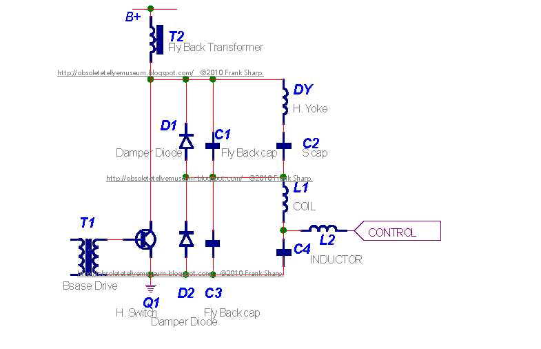
Simplified horizontal / line deflection circuit.
-------------------------------------------------------------------------------------------
A flyback transformer (FBT), also called a line output transformer (LOPT), is a special transformer, which is used for conversion of energy (current and voltage) in electronic circuits. It was initially designed to generate high current sawtooth signals at a relatively high frequency. In modern applications is used extensively in switched-mode power supplies for both low (3V) and high voltage (over 10 kV) supplies.
Flyback Transformer
It was invented as a means to control the horizontal movement of the electron beam in a cathode ray tube (CRT). Unlike conventional transformers, a flyback transformer is not fed with a signal of the same waveshape
as the intended output current. A convenient side effect of such a transformer is the considerable energy that is available in its magnetic circuit. This can be exploited using extra windings that can be used to provide power to operate other parts of the equipment. In particular, very high voltages are easily obtained using relatively few turns of winding which, once rectified, can provide the very high accelerating voltage for a CRT. Many more recent applications of such a transformer dispense with the need to produce high currents and just use the device as a relatively efficient means of producing a wide range of lower voltages using a transformer much smaller than a conventional mains transformer would be.
This GRUNDIG CHASSIS Series was featuring a Simplified BU208A based horizontal deflection section replacing all Thyristor horizontal timebase based circuits.

 A horizontal deflection circuit makes a sawtooth
current flow through a deflection coil. The current
will have equal amounts of positive and negative
current. The horizontal switch transistor conducts
for the right hand side of the picture. The damper
diode conducts for the left side of the picture.
Current only flows through the fly back capacitor
during retrace time.
For time 1 the transistor is turned on. Current
ramps up in the yoke. The beam is moved from the
center of the picture to the right edge. Energy is
stored on the inductance of the yoke.
E=I2L/2

For time 2 the transistor is turned off. Energy
transfers from the yoke to the flyback capacitor. At
the end of time two all the energy from the yoke is
placed on the flyback capacitor. There is zero
current in the yoke and a large voltage on the
capacitor. The beam is quickly moved from the
right edge back to the middle of the picture.
 During time 3 the energy on the capacitor flows
back into the yoke. The voltage on the flyback
capacitor decreases while the current in the yoke
builds until there is no voltage on the capacitor. By
the end of time 3 the yoke current is at it's
maximum amount but in the negative direction.
The beam is quickly deflected form the center to the
left edge.

Time 4 represents the left hand half of the picture.
Yoke current is negative and ramping down. The
beam moves from the left to the center of the
picture.
The current that flows when the horizontal switch is
closed is approximately:
Ipk ≅ Vcc T / Ldy
Ipk = collector current
T = 1/2 trace time
Ldy = total inductance (yoke + lin coil + size coil)
note:The lin coil inductance varies with current.
______
Tr ≅ 3.14 √ L C
The current that flows during retrace is produced by
the C and L oscillation. The retrace time is 1/2 the
oscillation frequency of the L and C.
I2L /2 ≅ V2C /2 or I2L = V2C As stated earlier the energy in the yoke moves to the
flyback capacitor during time 2.
V= the amount of the flyback pulse that is above the
supply voltage.
 D.C. annualizes is inductors are considered
shores, capacitors are open and generally
semiconductors are removed. The voltage at the
point “B+” is the supply voltage. The collector
voltage of Q1 is also at the supply voltage. The
voltage across C2 is equal to the supply voltage.
When we A.C. annualize this circuit we will find
that the collector of Q1 has a voltage that ranges
from slightly negative to 1000 volts positive. The
average voltage must remain the same as the D.C.
value.
In the A.C. annualizes of the circuit, the
inductance of the yoke (DY) and the inductance of
the flyback transformer are in parallel. The
inductance of T2 is much larger than that if the
DY. This results is a total system inductance of
about 10% to 20% less than that of the DY it’s
self.
The voltage across the Q1 is a half sinusoid pulse during the flyback or retrace period and close to zero at
all other times. It is not possible or safe to observe this point on an oscilloscope without a proper high
frequency high voltage probe. Normally use a 100:1 probe suitable for 2,000V peak. The probe must have
been high frequency calibrated recently.
HORIZONTAL SIZE / E/W AMPLITUDE - CORRECTION CIRCUIT:
There are several different methods of adjusting horizontal size.
 SIZE COIL
Add a variable coil to the yoke current path
causes the total inductance to vary with the coils
setting.
The yoke current is related to supply voltage,
trace time and total inductance. This method
has a limited range!
The horizontal section uses a PWM to set the
horizontal size. One DAC sets the horizontal
size and another DAC sets the pincushion and
trap.
The Raster Centering (D.C. centering) is
controlled by a DAC.
On small monitors the retrace time is fixed. On
large monitors or wide frequency range monitors
two different retrace times are available. The flyback time is set by the micro computer by selecting two
different flyback capacitors. At slow frequencies the longer retrace time is selected.
Different S corrector capacitor values are selected by the micro computer. At the highest frequency the
smallest capacitor is selected.
 SPLIT DIODE MODULATOR
This horizontal circuit consists of two parts. D1, C1, C2 and DY are the components as described above.
D2, C3, C4 and L1 are a second “dummy” horizontal section that does not cause deflection current. By the
D.C. analyzing this circuit the voltage across C2 + C4 must equal the supply voltage (B+). Deflection
current in the DY is related to the supply voltage minus the voltage across C4. For a maximum horizontal
size the control point must be held at ground. This causes the dummy section to not operate and the DY
section will get full supply voltage. If the control point is at 1/3 supply then the DY section will be
operating at 2/3 supply.
Note: The impedance of (D1,C1,C2 and DY) and (D2,C3,C4 and L1) makes a voltage divider. If the
control point is not connected then there is some natural voltage on C4. Most split diode monitors are built
to pull power from the dummy section through L2 to ground. A single power transistor shunts from the
control point to ground. It is true that power can be supplied from some other supply through L2 to rise the voltage on C4. For maximum range a bi-directional power amplifier can drive the control point.
The most exciting feature if the split diode modulator is that the flyback pulse, as seen by the flyback
transformer, is the same size at all horizontal size settings.
HORIZONTAL SWITCH/DAMPER DIODEOn the right hand side of the screen, the H. switch transistor conducts current through the deflection yoke.
This current comes from the S correction capacitors, which have a charge equal to the effective supply
voltage. The damper diode allows current for the left hand side of the screen to flow back through the
deflection yoke to the S capacitors.
FLYBACK CAPACITOR
The flyback capacitor connects the hot side of the yoke to ground. This component determines the size and
length of the flyback pulse. ‘Tuning the flyback capacitor’ is done to match the timing of the flyback pulse
to the video blanking time of the video signal. The peak flyback voltage on the horizontal switch must be
set to less that 80% if the Vces specification. The two conditions of time and voltage can be set by three
variables (supply voltage, retrace capacitor and yoke inductance) .
S CAPACITOR
The S capacitors corrects outside versus center linearity in the horizontal scan. The voltage on the S cap
has a parabola plus the DC horizontal supply. Reducing the value of S cap increases this parabola thus
reducing the size of the outside characters and increasing the size of the center characters.
S Capacitor value: Too low: picture will be squashed towards edges.
Too high: picture will be stretched towards edges.
By simply putting a capacitor in series with each coil, the sawtooth waveform is
modified into a slightly sine-wave shape. This reduces the scanning speed near the
edges where the yoke is more sensitive. Generally the deflection angle of the electron
beam and the yoke current are closely related. The problem is the deflection angle
verses the distance of movement on the CRT screen does not have a linear effect.
BASE DRIVE CURRENT
The base drive resistor determines the amount of
base drive. If the transistor is over driven the Vsat
looks very good, but the current fall time is poor.
If the base current is too small the current fall time is very fast. The problem is that the transistor will have many volts across C-E when closed.
The best condition is found by placing the transistor in the heaviest load condition. Adjust the base resistor for the least power consumption then increase the base drive a small amount. This will slightly over drive the base.
BU508(A)
Silicon NPNnpn transistors,pnp transistors,transistors
Category: NPN Transistor, Transistor
MHz: <1 MHz
Amps: 5A
Volts: 1500V
HIGH VOLTAGE CAPABILITY
JEDEC TO-3 METAL CASE.
DESCRIPTION
The BU208A, BU508A and BU508AFI are
manufactured using Multiepitaxial Mesa
technology for cost-effective high performance
and use a Hollow Emitter structure to enhance
switching speeds.
APPLICATIONS:
* HORIZONTAL DEFLECTION FOR COLOUR TV With 110° or even 90° degree of deflection angle.
ABSOLUTE MAXIMUM RATINGS
Symbol Parameter Value Unit
VCES Collector-Emit ter Voltage (VBE = 0) 1500 V
VCEO Collector-Emit ter Voltage (IB = 0) 700 V
VEBO Emitter-Base Voltage (IC = 0) 10 V
IC Collector Current 8 A
ICM Collector Peak Current (tp < 5 ms) 15 A
TO - 3 TO - 218 ISOWATT218
Ptot Total Dissipation at Tc = 25 oC 150 125 50 W
Tstg Storage Temperature -65 to 175 -65 to 150 -65 to 150 oC
Tj Max. Operating Junction Temperature 175 150 150 °C
----------------------------------------------------------------------------------
FRAME Deflection Output with IC TDA3650 (PHILIPS)GENERAL DESCRIPTION
TDA3650 is a monolithic integrated circuit for vertical deflection in large screen colour television
receivers.
The circuit incorporates the following functions:
• Oscillator
• Synchronization circuit
• Blanking pulse generator
• Sawtooth generator
• $-correction and linearity control
• Comparator and drive circuit
• Output stage
• Flyback generator
• Voltage stabilizer
• Thermal protection circuit
• Guard circuit
• Output stage protection
APPLICATION INFORMATION
The function is described against the corresponding pin number.
1. Comparator and drive circuit
The current flowing through the deflection coils is measured across an external series resistor. The signal
across this resistor is fed to the comparator via pin 1, where it is compared with the internally generated
sawtooth signal. The output of the comparator drives.the output stage. Pin 1 is also used for d.c. feed-
back of the output stage (mid-point setting).
2. Negative supply (ground) for the output stage
3. Output stage
The output stage provides the current to the deflection coils. The vertical deflection coil is connected
to this pin, via a series connection of a coupling capacitor and a feedback resistor to ground. The
output stage is protected against over-voltages and over-currents by a SOAR-protection circuit. When
one of the transistors exceeds its operational threshold the drive current is reduced to a safe level.
Temperature protection reduces the drive of the output stage when the junction temperature exceeds
170 oc.
4. Positive supply of output stage
This supply is obtained from the flyback generator. An electrolytic capacitor between pins 4 and 6, a
diode between pins 4 and 13, and a resistor between pins 6 and ground must be connected for correct
operation of the flyback generator.
5. Synchronization input
When the voltage applied to pin 5 reaches a level of 0, 7 V the lower switching level is increased thus
initiating the charge cycle of the oscillator capacitor. The synchronization circuit is inhibited during
oscillator flyback time.
6. Flyback generator
The flyback generator reduces power dissipation in the vertical stage. As a result a lower power supply
can be chosen (26 V for 30AX application). Whereas the voltage during flyback is increased to 45 V
(depending on the design of external components), the maximum increase of the voltage during fly back
is nearly factor 2.
The capacitor between pins 6 and 4 is charged via the external diode during the scan period. Then,
when the flyback generator is.activated by the oscillator flyback pulse, the voltage across the capacitor
is connected in series with the supply voltage to provide the required flyback voltage. At the end of the
oscillator pulse the drive of the flyback generator is maintained by the flyback voltage of the deflection
circuit.
7. Oscillator
The oscillator frequency is determined by the val.ues of the external resistor and capacitor connected
in parallel to pin 7. The capacitor is discharged via the resistor which is connected to ground. The
voltage on the capacitor is compared with an internal voltage from the voltage stabilizer (lower switching
level). When this loviter switching level is reached the capacitor is charged via an internal 500 n resistor.
At the same time the comparator voltage is increased (higher switching level). When the voltage on the
capacitor reaches the higher switching level the charge current is switched off and the capacitor is
discharged again.
8. S-correction and linearity circuit
From pin 8 an adjustable parabolic current is fed back to the mid-point of the sawtooth generator
capacitors at pin 9 to provide linearity control. The external components connected between pins 8
and 9 together with the d.c. feedback circuitry at pin 1 define the S-shape of the deflection current.
9. Sawtooth generator
The sawtooth signal is obtained by charging the capacitors connected to pin 9 via an external resistorVariation of the charge current will vary the amplitude of the signal. During oscillator flyback time
the capacitors are discharged to an internally fixed voltage level.
10. Output stage decoupling
A low value capacitor must be connected to pin 10 for decoupling of the output driver stage.
11. Blanking pulse generator
The blanking pulse duration is determined by the oscillator sawtooth signal. The guard circuit providcontinuous blanking when the vertical deflection current is absent.
12. Negative supply (ground) of small-signal part
13. Positive supply
The supply voltage at this pin is used to supply the flyback generator, the voltage stabilizer and the
protection circuits.
Chrominance + Luminance with PHILIPS TDA3561A,
PAL decoder TDA3561A
GENERAL DESCRIPTION

The PHILIPS TDA3561A is a decoder for the PAL colour television standard. It combines all functions required for the identification
and demodulation of PAL signals.
Furthermore it contains a luminance amplifier, an RGB-matrix and amplifier. These
amplifiers supply output signals up to 5 V peak-to-peak (picture information) enabling direct drive of the discrete output
stages.

The circuit also contains separate inputs for data insertion, analogue as well as digital, which can be used for text display systems (e.g. (Teletext/broadcast antiope), channel number display, etc. Additional to the TDA3560, the
circuit includes the following features:
· The peak white limiter is only active during the time that the 9,3 V level at the output is exceeded.
The start of the
limiting function is delayed by one line period. This avoids peak white limiting by test patterns which have abrupt transitions from colour to white signals.
· The brightness
control is obtained by inserting a variable pulse in the luminance
channel. Therefore the ratio of brightness variation and signal
amplitude at the three outputs will be identical and independent of the
difference in gain of the three channels. Thus discolouring due to
adjustment of contrast and brightness is avoided.
· Improved suppression of the internal RGB signals when the device is switched to external signals, and vice versa.
· Non-synchronized external RGB signals do not disturb the black level of the internal signals.
· Improved suppression of the residual 4,4 MHz signal in the RGB output stages.
· Cascoded stages in the demodulators and burst phase detector minimize the radiation of the colour demodulator
inputs.
· High current capability of the RGB outputs and the chrominance output.
APPLICATION INFORMATION
The function is described against the corresponding pin
number.
1. + 12 V power supply
The circuit gives good operation in a supply voltage range
between 8 and 13,2 V provided that the supply voltage for
the controls is equal to the supply voltage for the
TDA3561A. All signal and control levels have a linear
dependency on the supply voltage. The current taken by
the device at 12 V is typically 85 mA. It is linearly
dependent on the supply voltage.
2. Control voltage for identification
This pin requires a detection capacitor of about 330 nF for
correct operation. The voltages available under various
signal conditions are given in the specification.
3. Chrominance input
The chroma signal must be a.c.-coupled to the input.
Its amplitude must be between 55 mV and 1100 mV
peak-to-peak (25 mV to 500 mV peak-to-peak burst
signal). All figures for the chroma signals are based on a
colour bar signal with 75% saturation, that is the
burst-to-chroma ratio of the input signal is 1 : 2,25.
4. Reference voltage A.C.C. detector
This pin must be decoupled by a capacitor of about 330
nF. The voltage at this pin is 4,9 V.
5. Control voltage A.C.C.
The A.C.C. is obtained by synchronous detection of the
burst signal followed by a peak detector. A good noise
immunity is obtained in this way and an increase of the
colour for weak input signals is prevented. The
recommended capacitor value at this pin is 2,2 µF.
6. Saturation control
The saturation control range is in excess of 50 dB.
The control voltage range is 2 to 4 V. Saturation control is
a linear function of the control voltage.
When the colour killer is active, the saturation control
voltage is reduced to a low level if the resistance of the
external saturation control network is sufficiently high.
Then the chroma amplifier supplies no signal to the
demodulator. Colour switch-on can be delayed by proper
choice of the time constant for the saturation control
setting circuit.
When the saturation control pin is connected to the power
supply the colour killer circuit is overruled so that the colour
signal is visible on the screen. In this way it is possible to
adjust the oscillator frequency without using a frequency
counter (see also pins 25 and 26).
7. Contrast control
The contrast control range is 20 dB for a control voltage
change from + 2 to + 4 V. Contrast control is a linear
function of the control voltage. The output signal is
suppressed when the control voltage is 1 V or less. If one
or more output signals surpasses the level of 9 V the peak
white limiter circuit becomes active and reduces the out
putsignals via the contrast control by discharging C2 via an
internal current sink.
8. Sandcastle and field blanking input
The output signals are blanked if the amplitude of the input
pulse is between 2 and 6,5 V. The burst gate and clamping
circuits are activated if the input pulse exceeds a level of
7,5 V.
The higher part of the sandcastle pulse should start just
after the sync pulse to prevent clamping of video signal on
the sync pulse. The width should be about 4 µs for proper
A.C.C. operation.
9. Video-data switching
The insertion circuit is activated by means of this input by
an input pulse between 1 V and 2 V. In that condition, the
internal RGB signals are switched off and the inserted
signals are supplied to the output amplifiers. If only normal
operation is wanted this pin should be connected to the
negative supply. The switching times are very short
(< 20 ns) to avoid coloured edges of the inserted signals
on the screen.
10. Luminance signal input
The input signal should have a peak-to-peak amplitude of
0,45 V (peak white to sync) to obtain a black-white output
signal to 5 V at nominal contrast. It must be a.c.-coupled to
the input by a capacitor of about 22 nF. The signal is
clamped at the input to an internal reference voltage.
A 1 kΩ luminance delay line can be applied because the
luminance input impedance is made very high.
Consequently the charging and discharging currents of the
coupling capacitor are very small and do not influence the
signal level at the input noticeably. Additionally the
coupling capacitor value may be small.
11. Brightness control
The black level of the RGB outputs can be set by the
voltage on this pin (see Fig.5). The black level can be set
higher than 4 V however the available output signal
amplitude is reduced (see pin 7). Brightness control also
operates on the black level of the inserted signals.
12, 14, 16. RGB outputs
The output circuits for red, green and blue are identical.
Output signals are 5,25 V (R, G and B) at nominal input
signals and control settings. The black levels of the three
outputs have the same value. The blanking level at the
outputs is 2,1 V. The peak white level is limited to 9,3 V.
When this level exceeded the output signal amplitude is
reduced via the contrast control (see pin 7).
13, 15, 17. Inputs for external RGB signals
The external signals must be a.c.-coupled to the inputs via
a coupling capacitor of about 100 nF. Source impedance
should not exceed 150 Ω. The input signal required for
a 5 V peak-to-peak output signal is 1 V peak-to-peak.
At the RGB outputs the black level of the inserted signal is
identical to that of normal RGB signals. When these inputs
are not used the coupling capacitors have to be connectedto the negative supply.
18, 19, 20. Black level clamp capacitors
The black level clamp capacitors for the three channels are
connected to these pins. The value of each capacitor
should be about 100 nF.
21, 22. Inputs (B-Y) and (R-Y) demodulators
The input signal is automatically fixed to the required level
by means of the burst phase detector and A.C.C.
generator which are connected to pin 21 and pin 22. As the
burst (applied differentially to those pins) is kept constant
by the A.C.C., the colour difference signals automatically
have the correct value.
23, 24. Burst phase detector outputs
At these pins the output of the burst phase detector is
filtered and controls the reference oscillator. An adequate
catching range is obtained with the time constants given in
the application circuit (see Fig.6).
25, 26. Reference oscillator
The frequency of the oscillator is adjusted by the variable
capacitor C1. For frequency adjustment interconnect pin
21 and pin 22. The frequency can be measured by
connecting a suitable frequency counter to pin 25.
28. Output of the chroma amplifier
Both burst and chroma signals are available at the output.
The burst-to-chroma ratio at the output is identical to that
at the input for nominal control settings. The burst signal is
not affected by the controls. The amplitude of the input
signal to the demodulator is kept constant by the A.C.C.
Therefore the output signal at pin 28 will depend on the
signal loss in the delay line.
Synchronization With TDA3576B.12V 70mA sync combination with transmitter identification and vertical 625 divider system
- Line deflection synchronized Power supply on the bottom of the cabinet !
TDA2541 IF AMPLIFIER WITH DEMODULATOR AND AFC

DESCRIPTION
The TDA2540 and 2541 are IF amplifier and A.M.
demodulator circuits for colour and black and white
television receivers using PNP or NPN tuners. They
are intended for reception of negative or positive
modulation CCIR standard.
They incorporate the following functions : .Gain controlled amplifier .Synchronous demodulator .White spot inverter .Video preamplifier with noise protection .Switchable AFC .AGC with noise gating .Tuner AGC output (NPN tuner for 2540)-(PNP
tuner for 2541) .VCR switch for video output inhibition (VCR
play back).
.SUPPLYVOLTAGE : 12V TYP
.SUPPLYCURRENT : 50mATYP
.I.F. INPUT VOLTAGE SENSITIVITY AT
F = 38.9MHz : 85mVRMS TYP
.VIDEO OUTPUT VOLTAGE (white at 10% of
top synchro) : 2.7VPP TYP
.I.F. VOLTAGE GAIN CONTROL RANGE :
64dB TYP .SIGNAL TO NOISE RATIO AT VI = 10mV :
58dB TYP
.A.F.C. OUTPUT VOLTAGE SWING FOR
Df = 100kHz : 10V TYP.
PHILIPS 20CT4426 /08Z SEGANTINI CHASSIS KT4 CIRCUIT ARRANGEMENT IN A PICTURE DISPLAY DEVICE UTILIZING A STABILIZED SUPPLY VOLTAGE CIRCUIT:CHASSIS KT4 Line synch Switched Mode Power Supply with Line deflection output Transistor Drive Circuit:
A
stabilized supply voltage circuit for a picture display device
comprising a chopper wherein the switching signal has the line frequency
and is duration-modulated. The coil of the chopper constitutes the
primary winding of a transformer a secondary winding of which drives
the line output transistor so that the switching transistor of the
chopper also functions as a driver for the line output stage. The
oscillator generating the switching signal may be the line oscillator.
In a special embodiment the driver and line output transistor
conduct simultaneously and in order to limit the base current of the
line output transistor a coil shunted by a diode is incorporated in
the drive line of the line output transistor. Other secondary
windings of the transformer drive diodes which conduct simultaneously
with the efficiency diode of the chopper so as to generate further
stabilized supply voltages.

 The
invention relates to a circuit arrangement in a picture display
device wherein the input direct voltage between two input terminals,
which is obtained be rectifying the mains alternating voltage, is
converted into a stabilized output direct voltage by means of a
switching transistor and a coil and wherein the transistor is connected
to a first input terminal and an efficiency diode is connected to the
junction of the transistor and the coil. The switching transistor is
driven by a pulsatory voltage of line frequency which pulses are
duration-modulated in order to saturate the switching transistor during
part of the period dependent on the direct voltage to be stabilized
and to cut off this transistor during the remaining part of the
period. The pulse duration modulation is effected by means of a
comparison circuit which compares the direct voltage to be stabilized
with a substantially constant voltage, the coil constituting the
primary winding of a transformer.
The
invention relates to a circuit arrangement in a picture display
device wherein the input direct voltage between two input terminals,
which is obtained be rectifying the mains alternating voltage, is
converted into a stabilized output direct voltage by means of a
switching transistor and a coil and wherein the transistor is connected
to a first input terminal and an efficiency diode is connected to the
junction of the transistor and the coil. The switching transistor is
driven by a pulsatory voltage of line frequency which pulses are
duration-modulated in order to saturate the switching transistor during
part of the period dependent on the direct voltage to be stabilized
and to cut off this transistor during the remaining part of the
period. The pulse duration modulation is effected by means of a
comparison circuit which compares the direct voltage to be stabilized
with a substantially constant voltage, the coil constituting the
primary winding of a transformer.
Such a circuit arrangement is known from German "Auslegeschrift" 1.293.304. wherein a circuit arrangement is described which has for its object to convert an input direct voltage which is generated between two terminals into a different direct voltage. The circuit employs a switch connected to the first terminal of the input voltage and periodically opens and closes so that the input voltage is converted into a pulsatory voltage. This pulsatory voltage is then applied to a coil. A diode is arranged between the junction of the switch and the coil and the second terminal of the input voltage whilst a load and a charge capacitor in parallel thereto are arranged between the other end of the coil and the second terminal of the input voltage. The assembly operates in accordance with the known efficiency principle i.e., the current supplied to the load flows alternately through the switch and through the diode. The function of the switch is perform
 ed
by a switching transistor which is driven by a periodical pulsatory
voltage which saturates this transistor for a given part of the
period. Such a configuration is known under different names in the
literature; it will be referred to herein as a "chopper." A known
advantage thereof, is that the switching transistor must be able to
stand a high voltage or provide a great current but it need not
dissipate a great power. The output voltage of the chopper is
compared with a constant reference voltage. If the output voltage
attempts to vary because the input voltage and/or the load varies, a
voltage causing a duration modulation of the pulses is produced at
the output of the comparison arrangement. As a result the quantity of
the energy stored in the coil varies and the output voltage is
maintained constant. In the German "Auslegeschrift" referred to it is
therefore an object to provide a stabilized supply voltage device.
ed
by a switching transistor which is driven by a periodical pulsatory
voltage which saturates this transistor for a given part of the
period. Such a configuration is known under different names in the
literature; it will be referred to herein as a "chopper." A known
advantage thereof, is that the switching transistor must be able to
stand a high voltage or provide a great current but it need not
dissipate a great power. The output voltage of the chopper is
compared with a constant reference voltage. If the output voltage
attempts to vary because the input voltage and/or the load varies, a
voltage causing a duration modulation of the pulses is produced at
the output of the comparison arrangement. As a result the quantity of
the energy stored in the coil varies and the output voltage is
maintained constant. In the German "Auslegeschrift" referred to it is
therefore an object to provide a stabilized supply voltage device.In the circuit arrangement according to the mentioned German "Auslegeschrift" the frequency of the load variations or a harmonic thereof is chosen as the frequency for the switching voltage. Particularly when the load fed by the chopper is the line deflection circuit of a picture display device, wherein thus the impedance of the load varies in the rhythm of the line frequency, the frequency of the switching voltage is equal to or is a multiple of the line frequency.
It
is to be noted that the chopper need not necessarily be formed as
that in the mentioned German "Auslegeschrift." In fact, it is known
from literature that the efficiency diode and the coil may be
exchanged. It is alternatively possible for the coil to be provided at
the first terminal of the input voltage whilst the switching
transistor is arranged between the other end and the second terminal
of the input voltage. The efficiency diode is then provided between
the junction of said end and the switching transistor and the load. It
may be recognized that for all these modifications a voltage is
present across the connections of the coil which voltage has the same
frequency and the same shape as the pulsatory switching voltage. The
control voltage of a line deflection circuit is a pulsatory voltage
which causes the line output transistor to be saturates and cut off
alternately. The invention is based on the recognition that the
voltage present across the connections of the coil is suitable to
function as such a control voltage and that the coil constitutes the
primary of a transformer. To this end the circuit arrangement
according to the invention is characterized in that a secondary
winding of the transformer drives the switching element which applies a
line deflection current to line deflection coils and by which the
voltage for the final anode of a picture display tube which forms part
of the picture display device is generated, and that the ratio
between the period during which the switching transistor is saturated
and the entire period, i.e., the switching transistor duty cycle is
between 0.3 and 0.7 during normal operation.The invention is also based on the recognition that the duration modulation which is necessary to stabilize the supply voltage with the switching transistor does not exert influence on the driving of the line output transistor. This resides in the fact that in case of a longer or shorter cut-off period of the line output transistor the current flowing through the line deflection coils thereof is not influenced because of the efficiency diode current and transistor current are taken over or, in case of a special kind of transistor, the collector-emitter current is taken over by the base collector current and conversely. However, in that case the above-mentioned ratios of 0.3 : 0.7 should be taken into account since otherwise this take-over principle is jeopardized.
As will be furth
er explained the use of the switching transistor as a driver for
the line output transistor in an embodiment to be especially
described hereinafter has the further advantage that the line output
transistor automatically becomes non-conductive when this switching
transistor is short circuited so that the deflection and the EHT for
the display tube drop out and thus avoid damage thereof.Due to the step according to the invention the switching transistor in the stabilized supply functions as a driver for the line deflection circuit. The circuit arrangement according to the invention may in addition be equipped with a very efficient safety circuit so that the reliability is considerably enhanced, which is described in the U.S. Pat. No. 3,629,686. The invention is furthermore based on the recognition of the fact that the pulsatory voltage present across the connections of the coil is furthermore used and to this end the circuit arrangement according to the invention is characterized in that secondary windings of the transformer drive diodes which conduct simultaneously with the efficiency diode so as to generate further stabilized direct voltages, one end of said diodes being connected to ground.
In order that the invention may be readily carried into effect, a few embodiments thereof will now be described in detail by way of example with reference to the accompanying diagrammatic drawings in which:
FIG. 1 shows a principle circuit diagram wherein the chopper and the line deflection circuit are further shown but other circuits are not further shown.
FIGS. 2a, 2b and 2c show the variation as a function of time of two currents and of a voltage occurring in the circuit arrangement according to FIG. 1.
FIGS. 3a 3b, 3c and 3d show other embodiments of the chopper.
FIGS. 4a and 4b show modifications of part of the circuit arrangement of FIG. 1.
 In
FIG. 1 the reference numeral 1 denotes a rectifier circuit which
converts the mains voltage supplied thereto into a non-stabilized direct
voltage. The collector of a switching transistor 2 is connected to
one of the two terminals between which this direct voltage is
obtained, said transistor being of the npn-type in this embodiment and
the base of which receives a pulsatory voltage which originates
through a control stage 4 from a modulator 5 and causes transistor 2
to be saturated and cut off alternately. The voltage waveform 3 is
produced at the emitter of transistor 2. In order to maintain the
output voltage of the circuit arrangement constant, the duration of
the pulses provided is varied in modulator 5. A pulse oscillator 6
supplies the pulsatory voltage to modulator 5 and is synchronized by a
signal of line frequency which originates from the line oscillator
6' present in the picture display device. This line oscillator 6' is
in turn directly synchronized in known manner by pulses 7' of line
frequency which are present in the device and originate for example
from a received television signal if the picture display device is a
television receiver. Pulse oscillator 6 thus generates a pulsatory
voltage the repetition frequency of which is the line frequency.
In
FIG. 1 the reference numeral 1 denotes a rectifier circuit which
converts the mains voltage supplied thereto into a non-stabilized direct
voltage. The collector of a switching transistor 2 is connected to
one of the two terminals between which this direct voltage is
obtained, said transistor being of the npn-type in this embodiment and
the base of which receives a pulsatory voltage which originates
through a control stage 4 from a modulator 5 and causes transistor 2
to be saturated and cut off alternately. The voltage waveform 3 is
produced at the emitter of transistor 2. In order to maintain the
output voltage of the circuit arrangement constant, the duration of
the pulses provided is varied in modulator 5. A pulse oscillator 6
supplies the pulsatory voltage to modulator 5 and is synchronized by a
signal of line frequency which originates from the line oscillator
6' present in the picture display device. This line oscillator 6' is
in turn directly synchronized in known manner by pulses 7' of line
frequency which are present in the device and originate for example
from a received television signal if the picture display device is a
television receiver. Pulse oscillator 6 thus generates a pulsatory
voltage the repetition frequency of which is the line frequency.
The emitter of switching transistor 2 is connected at one end to the cathode of an efficiency diode 7 whose other end is connected to the second input voltage terminal and at the other end to primary winding 8 of a transformer 9. Pulsatory voltage 3 which is produced at the cathode of efficiency diode 7 is clamped against the potential of said second terminal during the intervals when this diode conducts. During the other intervals the pulsatory voltage 3 assumes the value V i . A charge capacitor 10 and a load 11 are arranged between the other end of winding 8 and the second input voltage terminal. The elements 2,7,8,10 and 11 constitute a so-called chopper producing a direct voltage across charge capacitor 10, provided that capacitor 10 has a sufficiently great value for the line frequency and the current applied to load 11 flowing alternately through switching transistor 2 or through efficiency diode 7. The output voltage V o which is the direct voltage produced across charge capacitor 10 is applied to a comparison circuit 12 which compares the voltage V o with a reference voltage. Comparison circuit 12 generates a direct voltage which is applied to modulator 5 so that the duration of the effective period δ T of switching transistor 2 relative to the period T of pulses 3 varies as a function of the variations of output voltage V 0 . In fact, it is readily evident that output voltage V o is proportional to the ratio δ :
V o = V i . δ
Load 11 of the chopper consists in the consumption of parts of the picture display device which are fed by output voltage V 0 .
In a practical embodiment of the circuit arrangement according to
FIG. 1 wherein the mains alternating voltage has a nominal effective
value of 220 V and the rectified voltage V i is approximately 270 V, output voltage V o
for δ = 0.5 is approximately 135 V. This makes it also possible, for
example, to feed a line deflection circuit as is shown in FIG. 1
wherein load 11 then represents different parts which are fed by the
chopper. Since voltage V o is maintained constant due to
pulse duration modulation, the supply voltage of this line deflection
circuit remains constant with the favorable result that the line
amplitude(= the width of the picture displayed on the screen of the
picture display tube) likewise remains constant as well as the EHT
required for the final anode of the picture display tube in the same
circuit arrangement independent of the variations in the mains voltage
and the load on the EHT generator (= variations in brightness).However,
variations in the line amplitude and the EHT may occur as a result
of an insufficiently small internal impedance of the EHT generator.
Compensation means are known for this purpose. A possibility within
the scope of the present invention is to use comparison circuit 12
for this purpose. In fact, if the beam current passes through an
element having a substantially quadratic characteristic, for example,
a voltage-dependent resistor, then a variation for voltage V o
may be obtained through comparison circuit 12 which variation is
proportional to the root of the variation in the EHT which is a known
condition for the line amplitude to remain constant.In addition this facilitates smoothing of voltage V o since the repetition frequency of pulsatory voltage 3 is many times higher than that of the mains and a comparatively small value may be sufficient for charge capacitor 10. If charge capacitor 10 has a sufficiently high value for the line frequency, voltage V o is indeed a direct voltage so that a voltage having the same form as pulsatory voltage 3 is produced across the terminals of primary winding 8. Thus voltages which have the same shape as pulsatory voltage 3 but have a greater or smaller amplitude are produced across secondary windings 13, 14 of transformer 9 (FIG. 1 shows only 2 secondary windings but there may be more). The invention is based on the recognition that one end of each secondary winding is connected to earth while the other end thereof drives a diode, the winding sense of each winding and the direction of conductance of each diode being chosen to be such that these diodes conduct during the same period as does efficiency diode 7. After smoothing, stabilized supply voltages, for example, at terminal 15 are generated in this manner at the amplitudes and polarities required for the circuit arrangements pre
sent
in the picture display device. In FIG. 1 the voltage generated at
terminal 15 is, for example, positive relative to earth. It is to be
noted that the load currents of the supply voltages obtained in this
manner cause a reduction of the switching power which is economized by
efficiency diode 7. The sum of all diode currents including that of
diode 7 is in fact equal to the current which would flow through
diode 7 if no secondary winding were wound on transformer 9 and if no
simultaneous diode were used. This reduction may be considered an
additional advantage of the circuit arrangement according to the
invention, for a diode suitable for smaller powers may then be used.
However, it will be evident that the overall secondary load must not
exceed the primary load since otherwise there is the risk of
efficiency diode 7 being blocked so that stabilization of the
secondary supply voltages would be out of the question.It is to be noted that a parabola voltage of line frequency as shown at 28 is produced across the charge capacitor 10 if this capacitor is given a smaller capacitance so that consequently the so-called S-correction is established.
In FIG. 1 charge capacitors are arranged between terminals 15 etc. and earth so as to ensure that the voltages on these points are stabilized direct voltages. If in addition the mean value of the voltage on one of these terminals has been made equal to the effective value of the alternating voltage which is required for heating the filament of the picture display tube present in the picture display device, this voltage is suitable for this heating. This is a further advantage of the invention since the cheap generation of a stabilized filament voltage for the picture display tube has always been a difficult problem in transistorized arrangements.
A further advantage of the picture display device according to the invention is that transformer 9 can function as a separation transformer so that the different secondary windings can be separated from the mains and their lower ends can be connected to ground of the picture display device. The latter step makes it possible to connect a different apparatus such as, for example, a magnetic recording and/or playback apparatus to the picture display device without earth connection problems occurring.
In FIG. 1 the reference numeral 14 denotes a secondary winding of transformer 9 which in accordance with the previously mentioned recognition of the invention can drive line output transistor 16 of the line deflection circuit 17. Line deflection circuit 17 which is shown in a simplified form in FIG. 1 includes inter alia line deflection coils 18 and an EHT transformer 19 a secondary winding 20 of which serves for generating the EHT required for the acceleration anode of the picture display tube. Line deflection circuit 17 is fed by the output voltage V o of the chopper which voltage is stabilized due to the pulse duration modulation with all previously mentioned advantages. Line deflection circuit 17 corresponds, for example, to similar arrangements which have been described in U.S. Pat. No. 3,504,224 issued Mar. 31, 1970 to J.J. Reichgelt et al., U.S. patent application Ser. No. 737,009 filed June 14, 1968 by W. H. Hetterscheid and U.S. application Ser. No. 26,497 filed April 8, 1970 by W. Hetterscheid et al. It will be evident that differently formed lined deflection circuits are alternatively possible.
It will now be shown that secondary winding 14 can indeed drive a line deflection circuit so that switching transistor 2 can function as a driver for the line deflection. FIGS. 2a and b show the variation as a function of time of the current i C which flows in the collector of transistor 16 and of the drive voltage v 14 across the terminals of
secondary winding 14. During the flyback period (0, t 1 ) transistor 16 must be fully cut off because a high voltage peak is then produced at its collector; voltage v 14 must then be absolutely negative. During the scan period (t 1 , t 4 ) a sawtooth current i C
flows through the collector electrode of transistor 16 which current
is first negative and then changes its direction. As the circuit
arrangement is not free from loss, the instant t 3 when current i C becomes zero lies, as is known, before the middle of the scan period. At the end t 4
of the scan period transistor 16 must be switched off again.
However, since transistor 16 is saturated during the scan period and
since this transistor must be suitable for high voltages and great
powers so that its collector layer is thick, this transistor has a
very great excess of charge carriers in both its base and collector
layers. The removal of these charge carriers takes a period t s
which is not negligible whereafter the transistor is indeed switched
off. Thus the fraction δ T of the line period T at which v 14 is positive must end at the latest at the instant (t 4 - t s ) located after the commencement (t = 0) of the previous flyback.The time δ T may be initiated at any instant t 2 which is located between the end t 1 of the flyback period and the instant t 3 when collector current i C reverses its direction. It is true that emitter current flows through transistor 16 at the instant t 2 , but collector current i C is not influenced thereby, at least not when the supply voltage (= V o ) for line deflection circuit 17 is high enough. All this has been described in the U.S. Pat. No. 3,504,224. The same applies to line deflection circuits wherein the collector base diode does not function as an efficiency diode as is the case in the described circuit 17, but wherein an efficiency diode is arranged between collector and emitter of the line output transistor. In such a case the negative part of the current i C of FIG. 2a represents the current flowing through the said efficiency diode.
After the instant t 3 voltage v 14 must be positive. In other words, the minimum duration of the period T when voltage v 14 must be positive is (t 4 - t s ) - t 3 whilst the maximum duration thereof is (t 4 - t s ) - t 1 . In a television system employing 625 lines per raster the line period t 4 is approximately 64 μus and the flyback period is approximately 12 μus. Without losses in the circuit arrangement instant t 3 would be located approximately 26 μus after the instant t 1 ,
and with losses a reasonable value is 22 μus which is 34 μus after
the commencement of the period. If for safety's sake it is assumed
that t s lasts approximately 10 μus, the extreme values of
δ T are approximately 20 and 42 μus and consequently the values for δ
are approximately 0.31 and 0.66 at a mean value which is equal to
approximately 0.49. It was previously stated that a mean value of δ =
0.5 was suitable. Line deflection circuit 17 can therefore indeed be
used in combination with the chopper in the manner described, and the
relative variation of δ may be (0.66 - 0.31) : 0.49 = 71.5 percent.
This is more than necessary to obviate the variations in the mains
voltage or in the various loads and to establish the East-West
modulation and ripple compensation to be described hereinafter. In
fact, if it is assumed that the mains voltage varies between -15 and
+10 percent of the nominal value of 220 V, while the 50 Hz ripple
voltage which is superimposed on the input voltage V i has a peak-to-peak value of 40 V and V i is nominally 270 V, then the lowest occurring V i is:0.85 × 270 V - 20 V = 210 V and the highest occurring V i is
1.1 × 270 V + 20 V = 320 V. For an output voltage V o of 135 V the ratio must thus vary between
δ = 135 : 210 = 0.64 and δ = 135 : 320 = 0.42.
A considerable problem presenting itself is that of the simultaneous or non-simultaneous drive of line output transistor 16 with switching transistor 2, it being understood that in case of simultaneous drive both transistors are simultaneously bottomed, that is during the period δ T. This depends on the winding sense of secondary winding 14 relative to that of primary winding 8. In FIG. 1 it has been assumed that the drive takes place simultaneously so that the voltage present across winding 14 has the shape shown in FIG. 2b. This voltage assumes the v
alue n(V i - V o ) in the
period δ T and the value -nVo in the period (1 - δ )T, wherein n is
the ratio of the number of turns on windings 14 and 8 and wherein V o is maintained constant at nominal mains voltage V o = δ V inom . However, if as a result of an increase or a decrease of the mains voltage V i increases or decreases proportionally therewith, i.e., V i = V i nom + Δ V, the positive portion of V 14 becomes equal to n(V i nom - V o +Δ V) = n [(1 -δ)V i nom +ΔV] = n(0.5 V inom +ΔV) if δ = 0.5 for V i = V i nom. Relatively, this is a variation which is twice as great. For example, if V i nom = 270 V and V o = 135 V, a variation in the mains voltage of from -15 to +10 percent causes a variation of V i
of from -40.5 V to +27 V which ranges from -30 to +20 percent of 135
V which is present across winding 8 during the period δ T. The
result is that transistor 16 can always be bottomed over a large
range of variation. If the signal of FIG. 2b would be applied through
a resistor to the base of transistor 16, the base current thereof
would have to undergo the same variation while the transistor would
already be saturated in case of too low a voltage. In this case it is
assumed that transformer 9 is ideal (without loss) and that coil 21
has a small inductance as is explained in the U.S. patent application
Ser. No. 737,009 above mentioned. It is therefore found to be
desirable to limit the base current of transistor 16.This may be effected by providing a coil 22 having a large value inductance, approximately 100 μH, between winding 14 and the small coil 21. The variation of said base current i b is shown in FIG. 2c but not to the same scale as the collector current of FIG. 2a. During the conducting interval δ T current i b varies as a linear function of time having a final value of wherein L represents the inductance of coil 22. This not only provides the advantage that this final value is not immediately reached, but it can be shown that variation of this final value as a function of the mains voltage has been reduced, for there applies at nominal mains voltage that: If the mains voltage V i = V i nom +Δ V, then ##SPC1## because V i nom = 2 V o . Thus this variation is equal to that of the mains voltage and is not twice as great.
 During switching off, t 2 ,
of transistor 16 coil 22 must exert no influence and coil 21 must
exert influence which is achieved by arranging a diode 23 parallel to
coil 22. Furthermore the control circuit of transistor 16 in this
example comprises the two diodes 24 and 25 as described in U.S.
application Ser. No. 26,497 above referred to, wherein one of these
diodes, diode 25 in FIG. 1, must be shunted by a resistor.
During switching off, t 2 ,
of transistor 16 coil 22 must exert no influence and coil 21 must
exert influence which is achieved by arranging a diode 23 parallel to
coil 22. Furthermore the control circuit of transistor 16 in this
example comprises the two diodes 24 and 25 as described in U.S.
application Ser. No. 26,497 above referred to, wherein one of these
diodes, diode 25 in FIG. 1, must be shunted by a resistor.
The control circuit of transistor 16 may alternatively be formed as is shown in FIG. 4. In fact, it is known that coil 21 may be replaced by the parallel arrangement of a diode 21' and a resistor 21" by which the inverse current can be limited. To separate the path of the inverse current from that of the forward current the parallel arrangement of a the diode 29' and a resistor 29" must then be present. This leads to the circuit arrangement shown in the upper part of FIG. 4. This circuit arrangement may now be simplified if it is noted that diodes 25 and 21' on the one hand and diodes 23 and 29' on the other hand are series-arranged. The result is shown in the lower part of FIG. 4 which, as compared with the circuit arrangement of FIG. 1, employs one coil less and an additional resistor.
FIG. 3 shows possible modifications of the chopper. FIG. 3a shown in a simplified form the circuit arrangement according to FIG. 1 wherein the pulsatory voltage present across the connections of windings 8 has a peak-to-peak amplitude of V i - V o = 0.5 V i for δ = 0.5, As has been stated, the provision of coil 22 gives a relative variation for the base current of transistor 16 which is equal to that of the mains voltage. In the cases according to FIG. 3b, 3c and 3d the peak-to-peak amplitude of the voltage across winding 8 is equal to V i so that the provision of coil 22 results in a relative variation which is equal to half that of the mains voltage which is still more favorable than in the first case.
Transistors of the npn type are used in FIG. 3. If transistors of the pnp type are used, the relevant efficiency diodes must of course be reversed.
In this connection it is to be noted that it is possible to obtain an output voltage V o with the aid of the modifications according to FIGS. 3b, c and d, which voltage is higher than input voltage V i . These modifications may be used in countries such as, for example, the United of America or France where the nominal mains voltage is 117 or 110 V without having to modify the rest of the circuit arrangement.
The above-mentioned remark regarding the sum of the diode currents only applies, however, for the modifications shown in FIGS. 3a and d.
The line deflection circuit itself is also safeguarded: in fact, if something goes wrong in the supply, the driver voltage of the line deflection circuit drops out because the switching voltage across the terminals of primary winding 8 is no longer present so that the deflection stops. This particularly happens when switching transistor 2 starts to constitute a short-circuit between emitter and collector with the result that the supply voltage V o for the line deflection circuit in the case of FIG. 1 becomes higher, namely equal to V i . However, the line output transformer is now cut off and is therefore also safe as well as the picture display tube and other parts of the display device which are fed by terminal 15 or the like. However, this only applies to the circuit arrangement according to FIG. 1 or 3a.
 Pulse
oscillator 6 applies pulses of line frequency to modulator 5. It may
be advantageous to have two line frequency generators as already
described, to wit pulse oscillator 6 and line oscillator 6' which is
present in the picture display device and which is directly synchronized
in known manner by line synchronizing pulses 7'. In fact, in this
case line oscillator 6' applies a signal of great amplitude and free
from interference to pulse oscillator 6. However, it is alternatively
possible to combine pulse oscillator 6 and line oscillator 6' in one
single oscillator 6" (see FIG. 1) which results in an economy of
components. It will be evident that line oscillator 6' and oscillator 6"
may alternatively be synchronized indirectly, for example, by means
of a phase discriminator. It is to be noted neither pulse oscillator
6, line oscillator 6' and oscillator 6" nor modulator 5 can be fed by
the supply described since output voltage V o is still
not present when the mains voltage is switched on. Said circuit
arrangements must therefore be fed directly from the input terminals.
If as described above these circuit arrangements are to be separated
from the mains, a small separation transformer can be used whose
primary winding is connected between the mains voltage terminals and
whose secondary winding is connected to ground at one end and controls
a rectifier at the other end.
Pulse
oscillator 6 applies pulses of line frequency to modulator 5. It may
be advantageous to have two line frequency generators as already
described, to wit pulse oscillator 6 and line oscillator 6' which is
present in the picture display device and which is directly synchronized
in known manner by line synchronizing pulses 7'. In fact, in this
case line oscillator 6' applies a signal of great amplitude and free
from interference to pulse oscillator 6. However, it is alternatively
possible to combine pulse oscillator 6 and line oscillator 6' in one
single oscillator 6" (see FIG. 1) which results in an economy of
components. It will be evident that line oscillator 6' and oscillator 6"
may alternatively be synchronized indirectly, for example, by means
of a phase discriminator. It is to be noted neither pulse oscillator
6, line oscillator 6' and oscillator 6" nor modulator 5 can be fed by
the supply described since output voltage V o is still
not present when the mains voltage is switched on. Said circuit
arrangements must therefore be fed directly from the input terminals.
If as described above these circuit arrangements are to be separated
from the mains, a small separation transformer can be used whose
primary winding is connected between the mains voltage terminals and
whose secondary winding is connected to ground at one end and controls
a rectifier at the other end.
Capacitor 27 is
arranged parallel to efficiency diode 7 so as to reduce the
dissipation in switching transistor 2. In fact, if transistor 2 is
switched off by the pulsatory control voltage, its collector current
decreases and its collector-emitter voltage increases simultaneously
so that the dissipated power is not negligible before the collector
current has becomes zero. If efficiency diode 7 is shunted by
capacitor 27 the increase of the collector-emitter voltage is delayed
i.e., this voltage does not assume high values until the collector
current has already been reduced. It is true that in that case the
dissipation in transistor 2 slightly increases when it is switched on
by the pulsatory control voltage but on the other hand since the
current flowing through diode 7 has decreased due to the presence of the
secondary windings, its inverse current is also reduced when
transistor 2 is switched on and hence its dissipation has become
smaller. In addition it is advantageous to delay these switching-on and
switching-off periods to a slight extent because the switching
pulses then contain fewer Fourier components of high frequency which
may cause interferences in the picture display device and which may
give rise to visible interferences on the screen of the display tube.
These interferences occupy a fixed position on the displayed image
because the switching frequency is the line frequency which is less
disturbing to the viewer. In a practical circuit wherein the line
frequency is 15,625 Hz and wherein switching transistor 2 is an
experimental type suitable for a maximum of 350 V collector-emitter
voltage or 1 A collector current and wherein efficiency diode 7 is of
the Philips type BA 148 the capacitance of capacitor 27 is
approximately 680 pF whilst the load is 70 W on the primary and 20 W
on the secondary side of transformer 9. The collector dissipation
upon switching off is 0.3 W (2.5 times smaller than without capacitor
27) and 0.7 W upon switching on.As is known the so-called pincushion distortion is produced in the picture display tubes having a substantially flat screen and large deflection angles which are currently used. This distortion is especially a problem in color television wherein a raster correction cannot be brought about by magnetic means. The correction of the so-called East-West pincushion distortion i.e., in the horizontal direction on the screen of the picture display tube can be established in an elegant manner with the aid of the circuit arrangement according to the invention. In fact, if the voltage generated by comparison circuit 12 and being applied to modulator 5 for duration-modulating pulsatory voltage 3 is modulated by a parabola voltage 28 of field frequency, pulsatory voltage 3 is also modulated thereby. If the power consumption of the line deflection circuit forms part of the load on the output voltage of the chopper, the signal applied to the line deflection coils is likewise modulated in the same manner. Conditions therefore are that the parabola voltage 28 of field frequency has a polarity such that the envelope of the sawtooth current of line frequency flowing through the line deflection coils has a maximum in the middle of the scan of the field period and that charge capacitor 10 has not too small an impedance for the field frequency. On the other hand the other supply voltages which are generated by the circuit arrangement according to the invention and which might be hampered by this component of field frequency must be smoothed satisfactorily.
A practical embodiment of the described example with the reference numerals given provides an output for the supply of approximately 85 percent at a total load of 90 W, the internal resistance for direct current loads being 1.5 ohms and for pulsatory currents being approximately 10 ohms. In case of a variation of ± 10 percent of the mains voltage, output voltage V o is stable within 0.4 V. Under the nominal circumstances the collector dissipation of switching transistor 2 is approximately 2.5 W.
Since the internal resistance of the su
pply is so small, it can be used
advantageously, for example, at terminal 15 for supplying a class-B
audio amplifier which forms part of the display device. Such an
amplifier has the known advantages that its dissipation is directly
proportional to the amplitude of the sound to be reproduced and that
its output is higher than that of a class-A amplifier. On the other
hand a class-A amplifier consumes a substantially constant power so
that the internal resistance of the supply voltage source is of little
importance. However, if this source is highly resistive, the supply
voltage is modulated in the case of a class-B amplifier by the audio
information when the sound intensity is great which may detrimentally
influence other parts of the display device. This drawback is
prevented by means of the supply according to the invention.The 50 Hz ripple voltage which is superimposed on the rectified input voltage V i is compensated by comparison circuit 12 and modulator 5 since this ripple voltage may be considered to be a variation of input voltage V i . A further compensation is obtained by applying a portion of this ripple voltage with suitable polarity to comparison circuit 12. It is then sufficient to have a lower value for the smoothing capacitor which forms part of rectifier circuit 1 (see FIG. 3). The parabola voltage 28 of field frequency originating from the field time base is applied to the same circuit 12 so as to correct the East-West pincushion distortion.
The RC-5 infrared remote protocol was developed by Philips in the late 1980s as a semi-proprietary consumer IR (infrared) remote control communication protocol for consumer electronics. However, it was also adopted by most European manufacturers, as well as many US manufacturers of specialty audio and video equipment.
The RC-5 infrared remote protocol was developed by Philips in the late 1980s as a semi-proprietary consumer IR (infrared) remote control communication protocol for consumer electronics. However, it was also adopted by most European manufacturers, as well as many US manufacturers of specialty audio and video equipment.The advantage of the RC-5 protocol is that (when properly followed) any CD handset (for example) may be used to control any brand of CD player using the RC-5 protocol.
Protocol Details
The basics of the protocol are well known. The handset contains a keypad and a transmitter integrated circuit (IC) driving an IR LED. The command data is a bi-phase encoded bitstream modulating a 36 kHz carrier. (Often the carrier used is 38 kHz or 40 kHz, apparently due to misinformation about the actual protocol.) The IR signal from the transmitter is detected by a specialized IC with an integral photo-diode, and is amplified, filtered, and demodulated so that the receiving device can act upon the received command. RC-5 only provides a one-way link, with information traveling from the handset to the receiving unit.The command comprises 14 bits:
- A start bit, which is always logic 1 and allows the receiving IC to set the proper gain.
- A field bit, which denotes whether the command sent is in the lower field (logic 1 = 0 to 63 decimal) or the upper field (logic 0 = 64 to 127 decimal). The field bit was added later by Philips when it was realized that 64 commands per device were insufficient. Previously, the field bit was combined with the start bit. Many devices still use this original system.
- A control bit, which toggles with each button press. This allows the receiving device to distinguish between two successive button presses (such as "1", "1" for "11") as opposed to the user simply holding down the button and the repeating commands being interrupted by a person walking by, for example.
- A five-bit system address, that selects one of 32 possible systems.
- A six-bit command, that (in conjunction with the field bit) represents one of the 128 possible RC-5 commands.
PHILIPS RC-5 System and Command Codes:
While the protocol is well known and understood, what is not so well documented are the system number allocations and the actual RC-5 commands used for each system. The information provided below is the most complete and accurate information available at this time. It is from a printed document from Philips dated December 1992 that is unfortunately not available in electronic format (e.g., PDF), nor is an updated version available. This information is provided so that companies that wish to use the RC-5 protocol can use it properly, and avoid conflicts with other equipment that may or may not be using the correct system numbers and commands.This code has an instruction set of 2048 different instructions and is divided into 32 address
of each 64 instructions. Every kind of equipment use his own address,
so this makes it possible to change the volume of the TV without change the volume of the hifi.
The transmitted code is a dataword wich consists of 14 bits and is defined as:

2 startbits for the automatic gain control in the infrared receiver.
1 toggle bit (change everytime when a new button is pressed on the ir transmitter)
5 address bits for the systemaddress
6 instructionbits for the pressed key.
The Philips RC5 IR transmission protocol uses Manchester encoding of the message bits. Each pulse burst (mark – RC transmitter ON) is 889us in length, at a carrier frequency of 36kHz (27.7us). Logical bits are transmitted as follows:
- Logical '0' – an 889us pulse burst followed by an 889us space, with a total transmit time of 1.778ms
- Logical '1' – an 889us space followed by an 889us pulse burst, with a total transmit time of 1.778ms
When a key is pressed on the remote controller, the message frame transmitted consists of the following 14 bits, in order:
- two Start bits (S1 and S2), both logical '1'.
- a Toggle bit (T). This bit is inverted each time a key is released and pressed again.
- the 5-bit address for the receiving device
- the 6-bit command.
 The
address and command bits are each sent most significant bit first.
Figure 1 illustrates the format of a Philips RC5 IR transmission
frame, for an address of 05h (00101b) and a command of 35h (110101b).
The
address and command bits are each sent most significant bit first.
Figure 1 illustrates the format of a Philips RC5 IR transmission
frame, for an address of 05h (00101b) and a command of 35h (110101b).Figure 1. Example message frame using the Philips RC5 IR transmission protocol.
From Figure 1 we can see that it takes:
- 5.334ms to transmit the Start and Toggle bits (S1, S2 and T). Notice that, as the first half-bit of S1 is a space, the receiver will only notice the real start of the message frame after 889us.
- 8.89ms to transmit the 5 bits for the address
- 10.668ms to transmit the 6 bits for the command
- 24.892ms to fully transmit the actual message frame.
No comments:
Post a Comment
The most important thing to remember about the Comment Rules is this:
The determination of whether any comment is in compliance is at the sole discretion of this blog’s owner.
Comments on this blog may be blocked or deleted at any time.
Fair people are getting fair reply. Spam and useless crap and filthy comments / scrapers / observations goes all directly to My Private HELL without even appearing in public !!!
The fact that a comment is permitted in no way constitutes an endorsement of any view expressed, fact alleged, or link provided in that comment by the administrator of this site.
This means that there may be a delay between the submission and the eventual appearance of your comment.
Requiring blog comments to obey well-defined rules does not infringe on the free speech of commenters.
Resisting the tide of post-modernity may be difficult, but I will attempt it anyway.
Your choice.........Live or DIE.
That indeed is where your liberty lies.
Note: Only a member of this blog may post a comment.