
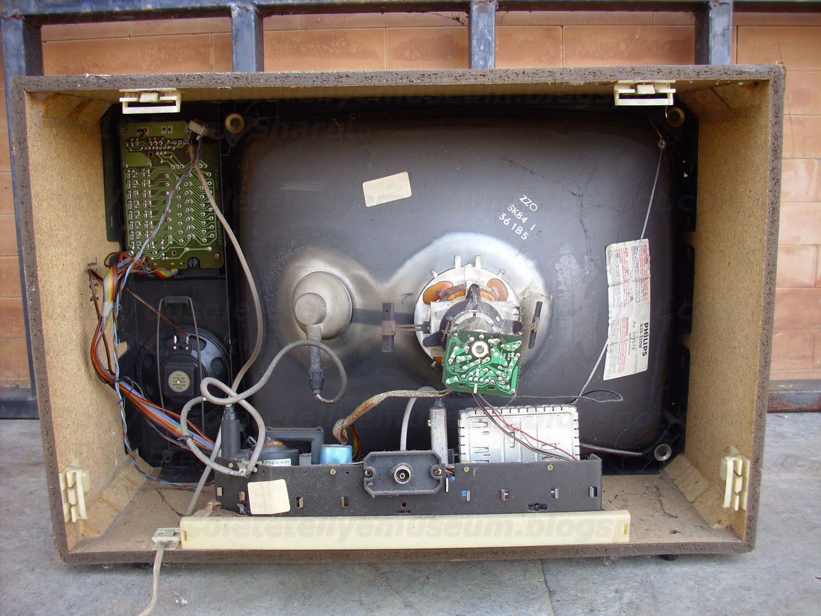


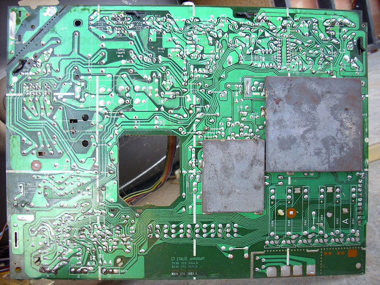
The PHILIPS CHASSIS L7 contains all functions of the receiver in a monocarrier PCB.
It's directly power supplyed by mains and is an example of a B/W chassis equipped with SMPS power supply type.
Mainly based on these here described circuits:
- TDA2577 Synchronization circuit with vertical oscillator and driver stages.
- TDA3190 COMPLETE TV SOUND CHANNEL
- TDA2541 IF


PHILIPS 20TL7021 /06Z ELBA CHASSIS L7 Synchronized switch-mode power supply:
In a switch mode power supply, a first switching
transistor is coupled to a primary winding of an isolation transformer.
A second switching transistor periodically applies a low impedance
across a second winding of the transformer that is coupled to an
oscillator for synchronizing the oscillator to the horizontal frequency.
A third winding of the transformer is coupled via a switching diode to a
capacitor of a control circuit for developing a DC control voltage in
the capacitor that varies in accordance with a supply voltage B+. The
control voltage is applied via the transformer to a pulse width
modulator that is responsive to the oscillator output signal for
producing a pulse-width modulated control signal. The control signal is
applied to a mains coupled chopper transistor for generating and
regulating the supply voltage B+ in accordance with the pulse width
modulation of the control signal.
Description:
The invention relates to switch-mode power supplies.
Some television receivers have signal terminals for receiving, for example, external video input signals such as R, G and B input signals, that are to be developed relative to the common conductor of the receiver. Such signal terminals and the receiver common conductor may be coupled to corresponding signal terminals and common conductors of external devices, such as, for example, a VCR or a teletext decoder.
To simplify the coupling of signals between the
external devices and the television receiver, the common conductors of
the receiver and of the external devices are connected together so that
all are at the same potential. The signal lines of each external device
are coupled to the corresponding signal terminals of the receiver. In
such an arrangement, the common conductor of each device, such as of the
television receiver, may be held "floating", or conductively isolated,
relative to the corresponding AC mains supply source that energizes the
device. When the common conductor is held floating, a user touching a
terminal that is at the potential of the common conductor will not
suffer an electrical shock.
Therefore, it may be desirable to isolate the common conductor, or ground, of, for example, the television receiver from the potentials of the terminals of the AC mains supply source that provide power to the television receiver. Such isolation is typically achieved by a transformer. The isolated common conductor is sometimes referred to as a "cold" ground conductor.
In a typical switch mode power supply (SMPS) of a television receiver the AC mains supply voltage is coupled, for example, directly, and without using transformer coupling, to a bridge rectifier. An unregulated direct current (DC) input supply voltage is produced that is, for example, referenced to a common conductor, referred to as "hot" ground, and that is conductively isolated from the cold ground conductor. A pulse width modulator controls the duty cycle of a chopper transistor switch that applies the unregulated supply voltage across a primary winding of an isolating flyback transformer. A flyback voltage at a frequency that is determined by the modulator is developed at a secondary winding of the transformer and is rectified to produce a DC output supply voltage such as a voltage B+ that energizes a horizontal deflection circuit of the television receiver. The primary winding of the flyback transformer is, for example, conductively coupled to the hot ground conductor. The secondary winding of the flyback transformer and voltage B+ may be conductively isolated from the hot ground conductor by the hot-cold barrier formed by the transformer.
It may be desirable to synchronize the operation of the chopper transistor to horizontal scanning frequency for preventing the occurrence of an objectionable visual pattern in an image displayed in a display of the television receiver.
It may be further desirable to couple a horizontal
synchronizing signal that is referenced to the cold ground to the
pulse-width modulator that is referenced to the hot ground such that
isolation is maintained.
A synchronized switch mode power supply, embodying an aspect of the invention, includes a transfromer having first and second windings. A first switching arrangement is coupled to the first winding for generating a first switching current in the first winding to periodically energize the second winding. A source of a synchronizing input signal at a frequency that is related to a deflection frequency is provided. A second switching arrangement responsive to the input signal and coupled to the second winding periodically applies a low impedance across the energized second winding that by transformer action produces a substantial increase in the first switching current. A periodic first control signal is generated. The increase in the first switching current is sensed to synchronize the first control signal to the input signal. An output supply voltage is generated from an input supply voltage in accordance with the first control signal.
PHILIPS 20TL7021 /06Z ELBA CHASSIS L7 CIRCUIT ARRANGEMENT IN A
PICTURE DISPLAY DEVICE UTILIZING A STABILIZED SUPPLY VOLTAGE CIRCUIT:
A stabilized supply voltage circuit for a picture display device comprising a chopper wherein the switching signal has the line frequency and is duration-modulated. The coil of the chopper constitutes the primary winding of a transformer a secondary winding of which drives the line output transistor so that the switching transistor of the chopper also functions as a driver for the line output stage. The oscillator generating the switching signal may be the line oscillator. In a special embodiment the driver and line output transistor conduct simultaneously and in order to limit the base current of the line output transistor a coil shunted by a diode is incorporated in the drive line of the line output transistor. Other secondary windings of the transformer drive diodes which conduct simultaneously with the efficiency diode of the chopper so as to generate further stabilized supply voltages.

 1. An electrical circuit
arrangement for a picture display device operating at a given line
scanning frequency, comprising a source of unidirectional voltage, an
inductor, first switching transistor means for periodically energizing
said inductor at said scanning frequency with current from said source,
an electrical load circuit coupled to said inductor and having applied
thereto a voltage as determined by the ratio of the ON and OFF periods
of said transistor, means for maintaining the voltage across said load
circuit at a given value comprising means for comparing the voltage of
said load circuit with a reference voltage, means responsive to
departures of the value of the load circuit voltage from the value of
said reference voltage for varying the conduction ratio of the ON and
OFF periods of said transistor thereby to stabilize said load circuit
voltage at the given value, a line deflection coil system for said
picture display device, means for energizing said line deflection coil
system from said load voltage circuit means, means for periodically
interrupting the energization of said line deflection coil comprising
second switching means and means coupled to said inductor for deriving
therefrom a switching current in synchronism with the energization
periods of said transistor and applying said switching
current to said switching means thereby to actuate the same, and means
coupled to said switching means and to said load voltage circuit for
producing a voltage for energizing said 2. A circuit as claimed in claim
1 wherein the duty cycle of said switching 3. A circuit as claimed in
claim 1 further comprising an efficiency first 4. A circuit as claimed
in claim 3 further comprising at least a second diode coupled to said
deriving means and to ground, and being poled to 5. A circuit as claimed
in claim 1 wherein said second switching means comprises a second
transistor coupled to said deriving means to conduct simultaneously with
said first transistor, and further comprising a coil coupled between
said driving means and said second transistor and a third diode shunt
coupled to said coil and being poled to conduct when said 6. A circuit
as claimed in claim 1 further comprising a horizontal oscillator coupled
to said first transistor, said oscillator being the 7. A circuit as
claimed in claim 1 further comprising means coupled to said inductor for
deriving filament voltage for said display device.
1. An electrical circuit
arrangement for a picture display device operating at a given line
scanning frequency, comprising a source of unidirectional voltage, an
inductor, first switching transistor means for periodically energizing
said inductor at said scanning frequency with current from said source,
an electrical load circuit coupled to said inductor and having applied
thereto a voltage as determined by the ratio of the ON and OFF periods
of said transistor, means for maintaining the voltage across said load
circuit at a given value comprising means for comparing the voltage of
said load circuit with a reference voltage, means responsive to
departures of the value of the load circuit voltage from the value of
said reference voltage for varying the conduction ratio of the ON and
OFF periods of said transistor thereby to stabilize said load circuit
voltage at the given value, a line deflection coil system for said
picture display device, means for energizing said line deflection coil
system from said load voltage circuit means, means for periodically
interrupting the energization of said line deflection coil comprising
second switching means and means coupled to said inductor for deriving
therefrom a switching current in synchronism with the energization
periods of said transistor and applying said switching
current to said switching means thereby to actuate the same, and means
coupled to said switching means and to said load voltage circuit for
producing a voltage for energizing said 2. A circuit as claimed in claim
1 wherein the duty cycle of said switching 3. A circuit as claimed in
claim 1 further comprising an efficiency first 4. A circuit as claimed
in claim 3 further comprising at least a second diode coupled to said
deriving means and to ground, and being poled to 5. A circuit as claimed
in claim 1 wherein said second switching means comprises a second
transistor coupled to said deriving means to conduct simultaneously with
said first transistor, and further comprising a coil coupled between
said driving means and said second transistor and a third diode shunt
coupled to said coil and being poled to conduct when said 6. A circuit
as claimed in claim 1 further comprising a horizontal oscillator coupled
to said first transistor, said oscillator being the 7. A circuit as
claimed in claim 1 further comprising means coupled to said inductor for
deriving filament voltage for said display device.
The
invention relates to a circuit arrangement in a picture display device
wherein the input direct voltage between two input terminals, which is
obtained be rectifying the mains alternating voltage, is converted into a
stabilized output direct voltage by means of a switching transistor and
a coil and wherein the transistor is connected to a first input
terminal and an efficiency diode is connected to the junction of the
transistor and the coil. The switching transistor is driven by a
pulsatory voltage of line frequency which pulses are duration-modulated
in order to saturate the switching transistor during part of the period
dependent on the direct voltage to be stabilized and to cut off this
transistor during the remaining part of the period. The pulse duration
modulation is effected by means of a comparison circuit which compares
the direct voltage to be sta bilized with a substantially constant voltage, the coil constituting the primary winding of a transformer.
 Such a circuit arrangement is known from German
"Auslegeschrift" 1.293.304. wherein a circuit arrangement is described
which has for its object to convert an input direct voltage which is
generated between two terminals into a different direct voltage. The
circuit employs a switch connected to the first terminal of the input
voltage and periodically opens and closes so that the input voltage is
converted into a pulsatory voltage. This pulsatory voltage is then
applied to a coil. A diode is arranged between the junction of the
switch and the coil and the second terminal of the input voltage whilst a
load and a charge capacitor in parallel thereto are arranged between
the other end of the coil and the second terminal of the input voltage.
The assembly operates in accordance with the known efficiency principle
i.e., the current supplied to the load flows alternately through the
switch and through the diode. The function of the switch is performed by
a switching transistor which is driven by a periodical pulsatory
voltage which saturates this transistor for a given part of the period.
Such a configuration is known under different names in the literature;
it will be referred to herein as a "chopper." A known advantage thereof,
is that the switching transistor must be able to stand a high voltage
or provide a great current but it need not dissipate a great power. The
output voltage of the chopper is compared with a constant reference
voltage. If the output voltage attempts to vary because the input
voltage and/or the load varies, a voltage causing a duration modulation
of the pulses is produced at the output of the comparison arrangement.
As a result the quantity of the energy stored in the coil varies and the
output voltage is maintained constant. In the German "Auslegeschrift"
referred to it is therefore an object to provide a stabilized supply
voltage device.
Such a circuit arrangement is known from German
"Auslegeschrift" 1.293.304. wherein a circuit arrangement is described
which has for its object to convert an input direct voltage which is
generated between two terminals into a different direct voltage. The
circuit employs a switch connected to the first terminal of the input
voltage and periodically opens and closes so that the input voltage is
converted into a pulsatory voltage. This pulsatory voltage is then
applied to a coil. A diode is arranged between the junction of the
switch and the coil and the second terminal of the input voltage whilst a
load and a charge capacitor in parallel thereto are arranged between
the other end of the coil and the second terminal of the input voltage.
The assembly operates in accordance with the known efficiency principle
i.e., the current supplied to the load flows alternately through the
switch and through the diode. The function of the switch is performed by
a switching transistor which is driven by a periodical pulsatory
voltage which saturates this transistor for a given part of the period.
Such a configuration is known under different names in the literature;
it will be referred to herein as a "chopper." A known advantage thereof,
is that the switching transistor must be able to stand a high voltage
or provide a great current but it need not dissipate a great power. The
output voltage of the chopper is compared with a constant reference
voltage. If the output voltage attempts to vary because the input
voltage and/or the load varies, a voltage causing a duration modulation
of the pulses is produced at the output of the comparison arrangement.
As a result the quantity of the energy stored in the coil varies and the
output voltage is maintained constant. In the German "Auslegeschrift"
referred to it is therefore an object to provide a stabilized supply
voltage device.
In the circuit arrangement according to the mentioned German "Auslegeschrift" the frequency of the load variations or a harmonic thereof is chosen as the frequency for the switching voltage. Particularly when the load fed by the chopper is the line deflection circuit of a picture display device, wherein thus the impedance of the load varies in the rhythm of the line frequency, the frequency of the switching voltage is equal to or is a multiple of the line frequency.
 It
is to be noted that the chopper need not necessarily be formed as that
in the mentioned German "Auslegeschrift." In fact, it is known from
literature that the efficiency diode and the coil may be exchanged. It
is alternatively possible for the coil to be provided at the first
terminal of the input voltage whilst the switching transistor is
arranged between the other end and the second terminal of the input
voltage. The efficiency diode is then provided between the junction of
said end and the switching transistor and the load. It may be recognized
that for all these modifications a voltage is present across the
connections of the coil which voltage has the same frequency and the
same shape as the pulsatory switching voltage. The control voltage of a
line deflection circuit is a pulsatory voltage which causes the line
output transistor to be saturates and cut off alternately. The invention
is based on the recognition that the voltage present across the
connections of the coil is suitable to function as such a control
voltage and that the coil constitutes the primary of a transformer. To
this end the circuit arrangement according to the invention is
characterized in that
a secondary winding of the transformer drives the switching element
which applies a line deflection current to line deflection coils and by
which the voltage for the final anode of a picture display tube which
forms part of the picture display device is generated, and that the
ratio between the period during which the switching transistor is
saturated and the entire period, i.e., the switching transistor duty
cycle is between 0.3 and 0.7 during normal operation.
It
is to be noted that the chopper need not necessarily be formed as that
in the mentioned German "Auslegeschrift." In fact, it is known from
literature that the efficiency diode and the coil may be exchanged. It
is alternatively possible for the coil to be provided at the first
terminal of the input voltage whilst the switching transistor is
arranged between the other end and the second terminal of the input
voltage. The efficiency diode is then provided between the junction of
said end and the switching transistor and the load. It may be recognized
that for all these modifications a voltage is present across the
connections of the coil which voltage has the same frequency and the
same shape as the pulsatory switching voltage. The control voltage of a
line deflection circuit is a pulsatory voltage which causes the line
output transistor to be saturates and cut off alternately. The invention
is based on the recognition that the voltage present across the
connections of the coil is suitable to function as such a control
voltage and that the coil constitutes the primary of a transformer. To
this end the circuit arrangement according to the invention is
characterized in that
a secondary winding of the transformer drives the switching element
which applies a line deflection current to line deflection coils and by
which the voltage for the final anode of a picture display tube which
forms part of the picture display device is generated, and that the
ratio between the period during which the switching transistor is
saturated and the entire period, i.e., the switching transistor duty
cycle is between 0.3 and 0.7 during normal operation.
The invention is also based on the recognition that the duration modulation which is necessary to stabilize the supply voltage with the switching transistor does not exert influence on the driving of the line output transistor. This resides in the fact that in case of a longer or shorter cut-off period of the line output transistor the current flowing through the line deflection coils thereof is not influenced because of the efficiency diode current and transistor current are taken over or, in case of a special kind of transistor, the collector-emitter current is taken over by the base collector current and conversely. However, in that case the above-mentioned ratios of 0.3 : 0.7 should be taken into account since otherwise this take-over principle is jeopardized.
As will be further explained the use of the switching transistor as a driver for the line output transistor in an embodiment to be especially described hereinafter has the further advantage that the line output transistor automatically becomes non-conductive when this switching transistor is short circuited so that the deflection and the EHT for the display tube drop out and thus avoid damage thereof.
Due to the step according to the invention the
switching transistor in the stabilized supply functions as a driver for
the line deflection circuit. The circuit arrangement according to the
invention may in addition be equipped with a very efficient safety
circuit so that the reliability is considerably enhanced, which is
described in the U.S. Pat. No. 3,629,686. The invention is furthermore
based on the recognition of the fact that the pulsatory voltage present
across the connections of the coil is furthermore used and to this end
the circuit arrangement according to the invention is characterized in
that secondary windings of the transformer drive diodes which conduct
simultaneously with the efficiency diode so as to generate further
stabilized direct voltages, one end of said diodes being connected to
ground.
In order that the invention may be readily carried into effect, a few embodiments thereof will now be described in detail by way of example with reference to the accompanying diagrammatic drawings in which:
FIG. 1 shows a principle circuit diagram wherein the chopper and the line deflection circuit are further shown but other circuits are not further shown.
FIGS. 2a, 2b and 2c show the variation as a function of time of two currents and of a voltage occurring in the circuit arrangement according to FIG. 1.
FIGS. 3a 3b, 3c and 3d show other embodiments of the chopper.
FIGS. 4a and 4b show modifications of part of the circuit arrangement of FIG. 1.
 In
FIG. 1 the reference numeral 1 denotes a rectifier circuit which
converts the mains voltage supplied thereto into a non-stabilized direct
voltage. The collector of a switching transistor 2 is connected to one
of the two terminals between which this direct voltage is obtained, said
transistor being of the npn-type in this embodiment and the base of
which receives a pulsatory voltage which originates through a control
stage 4 from a modulator 5 and causes transistor 2 to be saturated and
cut off alternately. The voltage waveform 3 is produced at the emitter
of transistor 2. In order to maintain the output voltage of the circuit
arrangement constant, the duration of the pulses provided is varied in
modulator 5. A pulse oscillator 6 supplies the pulsatory voltage to
modulator 5 and is synchronized by a signal of line frequency which
originates from the line oscillator 6' present in the picture display
device. This line oscillator 6' is in turn directly synchronized in
known manner by pulses 7' of line frequency which are present in the
device and originate for example from a received television signal if
the picture display device is a television receiver. Pulse oscillator 6
thus generates a pulsatory voltage the repetition frequency of which is
the line frequency.
In
FIG. 1 the reference numeral 1 denotes a rectifier circuit which
converts the mains voltage supplied thereto into a non-stabilized direct
voltage. The collector of a switching transistor 2 is connected to one
of the two terminals between which this direct voltage is obtained, said
transistor being of the npn-type in this embodiment and the base of
which receives a pulsatory voltage which originates through a control
stage 4 from a modulator 5 and causes transistor 2 to be saturated and
cut off alternately. The voltage waveform 3 is produced at the emitter
of transistor 2. In order to maintain the output voltage of the circuit
arrangement constant, the duration of the pulses provided is varied in
modulator 5. A pulse oscillator 6 supplies the pulsatory voltage to
modulator 5 and is synchronized by a signal of line frequency which
originates from the line oscillator 6' present in the picture display
device. This line oscillator 6' is in turn directly synchronized in
known manner by pulses 7' of line frequency which are present in the
device and originate for example from a received television signal if
the picture display device is a television receiver. Pulse oscillator 6
thus generates a pulsatory voltage the repetition frequency of which is
the line frequency.
The emitter of switching transistor 2 is connected at
one end to the cathode of an efficiency diode 7 whose other end is
connected to the second input voltage terminal and at the other end to
primary winding 8 of a transformer 9. Pulsatory voltage 3 which is
produced at the cathode of efficiency diode 7 is clamped against the
potential of said second terminal during the intervals when this diode
conducts. During the other intervals the pulsatory voltage 3 assumes the
value V i . A charge capacitor 10 and a load 11 are arranged
between the other end of winding 8 and the second input voltage
terminal. The elements 2,7,8,10 and 11 constitute a so-called chopper
producing a direct voltage across charge capacitor 10, provided that
capacitor 10 has a sufficiently great value for the line frequency and
the current applied to load 11 flowing alternately through switching
transistor 2 or through efficiency diode 7. The output voltage V o
which is the direct voltage produced across charge capacitor 10 is
applied to a comparison circuit 12 which compares the voltage V o with a reference voltage. Comparison circuit 12 generates a direct voltage which is applied
to modulator 5 so that the duration of the effective period δ T of
switching transistor 2 relative to the period T of pulses 3 varies as a
function of t he variations of output voltage V 0 . In fact, it is readily evident that output voltage V o is proportional to the ratio δ :
V o = V i . δ
Load 11 of the chopper consists in the consumption of parts of the picture display device which are fed by output voltage V 0 . In a practical embodiment of the circuit arrangement according to FIG. 1 wherein the mains alternating voltage has a nominal effective value of 220 V and the rectified voltage V i is approximately 270 V, output voltage V o for δ = 0.5 is approximately 135 V. This makes it also possible, for example, to feed a line deflection circuit as is shown in FIG. 1 wherein load 11 then represents different parts which are fed by the chopper. Since voltage V o is maintained constant due to pulse duration modulation, the supply voltage of this line deflection circuit remains constant with the favorable result that the line amplitude(= the width of the picture displayed on the screen of the picture display tube) likewise remains constant as well as the EHT required for the final anode of the picture display tube in the same circuit arrangement independent of the variations in the mains voltage and the load on the EHT generator (= variations in brightness).
However,
variations in the line amplitude and the EHT may occur as a result of
an insufficiently small internal impedance of the EHT generator.
Compensation means are known for this purpose. A possibility within the
scope of the present invention is to use comparison circuit 12 for this
purpose. In fact, if the beam current passes through an element having a
substantially quadratic characteristic, for example, a
voltage-dependent resistor, then a variation for voltage V o
may be obtained through comparison circuit 12 which variation is
proportional to the root of the variation in the EHT which is a known
condition for the line amplitude to remain constant.
In addition this facilitates smoothing of voltage V o since the repetition frequency of pulsatory voltage 3 is many times higher than that of the mains and a comparatively small value may be sufficient for charge capacitor 10. If charge capacitor 10 has a sufficiently high value for the line frequency, voltage V o is indeed a direct voltage so that a voltage having the same form as pulsatory voltage 3 is produced across the terminals of primary winding 8. Thus voltages which have the same shape as pulsatory voltage 3 but have a greater or smaller amplitude are produced across secondary windings 13, 14 of transformer 9 (FIG. 1 shows only 2 secondary windings but there may be more). The invention is based on the recognition that one end of each secondary winding is connected to earth while the other end thereof drives a diode, the winding sense of each winding and the direction of conductance of each diode being chosen to be such that these diodes conduct during the same period as does efficiency diode 7. After smoothing, stabilized supply voltages, f or example, at terminal 15
are generated in this manner at the amplitudes and polarities required
for the circuit arrangements present in the picture display device. In
FIG. 1 the voltage generated at terminal 15 is, for example, positive
relative to earth. It is to be noted that the load currents of the
supply voltages obtained in this manner cause a reduction of the
switching power which is economized by efficiency diode 7. The sum of
all diode currents including that of diode 7 is in fact equal to the
current which would flow through diode 7 if no secondary winding were
wound on transformer 9 and if no simultaneous diode were used. This
reduction may be considered an additional advantage of the circuit
arrangement according to the invention, for a diode suitable for smaller
powers may then be used. However, it will be evident that the overall
secondary load must not exceed the primary load since otherwise there is
the risk of efficiency diode 7 being blocked so that stabilization of
the secondary supply voltages would be out of the question.
or example, at terminal 15
are generated in this manner at the amplitudes and polarities required
for the circuit arrangements present in the picture display device. In
FIG. 1 the voltage generated at terminal 15 is, for example, positive
relative to earth. It is to be noted that the load currents of the
supply voltages obtained in this manner cause a reduction of the
switching power which is economized by efficiency diode 7. The sum of
all diode currents including that of diode 7 is in fact equal to the
current which would flow through diode 7 if no secondary winding were
wound on transformer 9 and if no simultaneous diode were used. This
reduction may be considered an additional advantage of the circuit
arrangement according to the invention, for a diode suitable for smaller
powers may then be used. However, it will be evident that the overall
secondary load must not exceed the primary load since otherwise there is
the risk of efficiency diode 7 being blocked so that stabilization of
the secondary supply voltages would be out of the question.
It is to be noted that a parabola voltage of line
frequency as shown at 28 is produced across the charge capacitor 10 if
this capacitor is given a smaller capacitance so that consequently the
so-called S-correction is established.
In FIG. 1 charge capacitors are arranged between terminals 15 etc. and earth so as to ensure that the voltages on these points are stabilized direct voltages. If in addition the mean value of the voltage on one of these terminals has been made equal to the effective value of the alternating voltage which is required for heating the filament of the picture display tube present in the picture display device, this voltage is suitable for this heating. This is a further advantage of the invention since the cheap generation of a stabilized filament voltage for the picture display tube has always been a difficult problem in transistorized arrangements.
A further advantage of the picture
display device according to the invention is that transformer 9 can
function as a separation transformer so that the different secondary
windings can be separated from the mains and their lower ends can be
connected to ground of the picture display device. The latter step makes
it possible to connect a different apparatus such as, for example, a
magnetic recording and/or playback apparatus to the picture display
device without earth connection problems occurring.
In FIG. 1 the reference numeral 14 denotes a secondary winding of transformer 9 which in accordance with the previously mentioned recognition of the invention can drive line output transistor 16 of the line deflection circuit 17. Line deflection circuit 17 which is shown in a simplified form in FIG. 1 includes inter alia line deflection coils 18 and an EHT transformer 19 a secondary winding 20 of which serves for generating the EHT required for the acceleration anode of the picture display tube. Line deflection circuit 17 is fed by the output voltage V o of the chopper which voltage is stabilized due to the pulse duration modulation with all previously mentioned advantages. Line deflection circuit 17 corresponds, for example, to similar arrangements which have been described in U.S. Pat. No. 3,504,224 issued Mar. 31, 1970 to J.J. Reichgelt et al., U.S. patent application Ser. No. 737,009 filed June 14, 1968 by W. H. Hetterscheid and U.S. application Ser. No. 26,497 filed April 8, 1970 by W. Hetterscheid et al. It will be evident that differently formed lined deflection circuits are alternatively possible.
It will now be shown that secondary winding 14 can indeed drive a line deflection circuit so that switching transistor 2 can function as a driver for the line deflection. FIGS. 2a and b show the variation as a function of time of the current i C which flows in the collector of transistor 16 and of the drive voltage v 14 across the terminals of secondary winding 14. During the flyback period (0, t 1 ) transistor 16 must be fully cut off because a high voltage peak is then produced at its collector; voltage v 14 must then be absolutely negative. During the scan period (t 1 , t 4 ) a sawtooth current i C
flows through the collector electrode of transistor 16 which current is
first negative and then changes its direction. As the circuit
arrangement is not free from loss, the instant t 3 when current i C becomes zero lies, as is known, before the middle of the scan period. At the end t 4
of the scan period transistor 16 must be switched off again. However,
since transistor 16 is saturated during the scan period and since this
transistor must be suitable for high voltages and great powers so that
its collector layer is thick, this transistor has a very great excess of
charge carriers in both its base and collector layers. The removal of
these charge carriers takes a period t s which is not
negligible whereafter the transistor is indeed switched off. Thus the
fraction δ T of the line period T at which v 14 is positive must end at the latest at the instant (t 4 - t s ) located after the commencement (t = 0) of the previous flyback.
The time δ T may be initiated at any instant t 2 which is located between the end t 1 of the flyback period and the instant t 3 when collector current i C reverses its direction. It is true that emitter current flows through transistor 16 at the instant t 2 , but collector current i C is not influenced thereby, at least not when the supply voltage (= V o )
for line deflection circuit 17 is high enough. All this has been
described in the U.S. Pat. No. 3,504,224. The same applies to line
deflection circuits wherein the collector base diode does not function
as an efficiency diode as is the case in the described circuit 17, but
wherein an efficiency diode is arranged between collector and emitter of
the line output transistor. In such a case the negative part of the
current i C of FIG. 2a represents the current flowing through the said efficiency diode.
After the instant t 3 voltage v 14 must be positive. In other words, the minimum duration of the period T when voltage v 14 must be positive is (t 4 - t s ) - t 3 whilst the maximum duration thereof is (t 4 - t s ) - t 1 . In a television system employing 625 lines per raster the line period t 4 is approximately 64 μus and the flyback period is approximately 12 μus. Without losses in the circuit arrangement instant t 3 would be located approximately 26 μus after the instant t 1 , and with losses a reasonable value is 22 μus which is 34 μus after the commencement of the period. If for safety's sake it is assumed that t s lasts approximately10
μus, the extreme values of δ T are approximately 20 and 42 μus and
consequently the values for δ are approximately 0.31 and 0.66 at a mean
value which is equal to approximately 0.49. It was previously stated
that a mean value of δ = 0.5 was suitable. Line deflection circuit 17
can therefore indeed be used in combination with the chopper in the
manner described, and the relative variation of δ may be (0.66 - 0.31) :
0.49 = 71.5 percent. This is more than necessary to obviate the
variations in the mains voltage or in the various loads and to establish
the East-West modulation and ripple compensation to be described
hereinafter. In fact, if it is assumed that the mains voltage varies
between -15 and +10 percent of the nominal value of 220 V, while the 50
Hz ripple voltage which is superimposed on the input voltage V i has a peak-to-peak value of 40 V and V i is nominally 270 V, then the lowest occurring V i is:
0.85 × 270 V - 20 V = 210 V and the highest occurring V i is
1.1 × 270 V + 20 V = 320 V. For an output voltage V o of 135 V the ratio must thus vary between
δ = 135 : 210 = 0.64 and δ = 135 : 320 = 0.42.
A considerable problem presenting itself is that of
the simultaneous or non-simultaneous drive of line output transistor 16
with switching transistor 2, it being understood that in case of
simultaneous drive both transistors are simultaneously bottomed, that is
during the period δ T. This depends on the winding sense of secondary
winding 14 relative to that of primary winding 8. In FIG. 1 it has been
assumed that the drive takes place simultaneously so that the voltage
present across winding 14 has the shape shown in FIG. 2b. This voltage
assumes the value n(V i - V o ) in the period δ T
and the value -nVo in the period (1 - δ )T, wherein n is the ratio of
the number of turns on windings 14 and 8 and wherein V o is maintained constant at nominal mains voltage V o = δ V inom . However, if as a result of an increase or a decrease of the mains voltage V i increases or decreases proportionally therewith, i.e., V i = V i nom + Δ V, the positive portion of V 14 becomes equal to n(V i nom - V o +Δ V) = n [(1 -δ)V i nom +ΔV] = n(0.5 V inom +ΔV) if δ = 0.5 for V i = V i nom. Relatively, this is a variation which is twice as great. For example, if V i nom = 270 V and V o = 135 V, a variation in the mains voltage of from -15 to +10 percent causes a variation of V i
of from -40.5 V to +27 V which ranges from -30 to +20 percent of 135 V
which is present across winding 8 during the period δ T. The result is
that transistor 16 can always be bottomed over a large range of
variation. If the signal of FIG. 2b would be applied through a resistor
to the base of transistor 16, the base current thereof
would have to undergo the same variation while the transistor would
already be saturated in case of too low a voltage. In this case it is
assumed that transformer 9 is ideal (without loss) and that coil 21 has a
small inductance as is explained in the U.S. patent application Ser.
No. 737,009 above mentioned. It is therefore found to be desirable to
limit the base current of transistor 16.
This may be effected by providing a coil 22 having a large value inductance, approximately 100 μH, between winding 14 and the small coil 21. The variation of said base current i b is shown in FIG. 2c but not to the same scale as the collector current of FIG. 2a. During the conducting interval δ T current i b varies as a linear function of time having a final value of wherein L represents the inductance of coil 22. This not only provides the advantage that this final value is not immediately reached, but it can be shown that variation of this final value as a function of the mains voltage has been reduced, for there applies at nominal mains voltage that: If the mains voltage V i = V i nom +Δ V, then ##SPC1## because V i nom = 2 V o . Thus this variation is equal to that of the mains voltage and is not twice as great.
 During switching off, t 2 ,
of transistor 16 coil 22 must exert no influence and coil 21 must exert
influence which is achieved by arranging a diode 23 parallel to coil
22. Furthermore the control circuit of transistor 16 in this example
comprises the two diodes 24 and 25 as described in U.S. application Ser.
No. 26,497 above referred to, wherein one of these diodes, diode 25 in
FIG. 1, must be shunted by a resistor.
During switching off, t 2 ,
of transistor 16 coil 22 must exert no influence and coil 21 must exert
influence which is achieved by arranging a diode 23 parallel to coil
22. Furthermore the control circuit of transistor 16 in this example
comprises the two diodes 24 and 25 as described in U.S. application Ser.
No. 26,497 above referred to, wherein one of these diodes, diode 25 in
FIG. 1, must be shunted by a resistor.
The control circuit of transistor 16 may alternatively be formed as is shown in FIG. 4. In fact, it is known that coil 21 may be replaced by the parallel arrangement of a diode 21' and a resistor 21" by which the inverse current can be limited. To separate the path of the inverse current from that of the forward current the parallel arrangement of a the diode 29' and a resistor 29" must then be present. This leads to the circuit arrangement shown in the upper part of FIG. 4. This circuit arrangement may now be simplified if it is noted that diodes 25 and 21' on the one hand and diodes 23 and 29' on the other hand are series-arranged. The result is shown in the lower part of FIG. 4 which, as compared with the circuit arrangement of FIG. 1, employs one coil less and an additional resistor.
FIG. 3 shows possible modifications of the chopper. FIG. 3a shown in a simplified form the circuit arrangement according to FIG. 1 wherein the pulsatory voltage present across the connections of windings 8 has a peak-to-peak amplitude of V i - V o = 0.5 V i for δ = 0.5, As has been stated, the provision of coil 22 gives a relative variation for the base current of transistor 16 which is equal to that of the mains voltage. In the cases according to FIG. 3b, 3c and 3d the peak-to-peak amplitude of the voltage across winding 8 is equal to V i so that the provision of coil 22 results in a relative variation which is equal to half that of the mains voltage which is still more favorable than in the first case.
Transistors
of the npn type are used in FIG. 3. If transistors of the pnp type are
used, the relevant efficiency diodes must of course be reversed.
In this connection it is to be noted that it is possible to obtain an output voltage V o with the aid of the modifications according to FIGS. 3b, c and d, which voltage is higher than input voltage V i . These modifications may be used in countries such as, for example, the United of America or France where the nominal mains voltage is 117 or 110 V without having to modify the rest of the circuit arrangement.
The above-mentioned remark regarding the sum of the diode currents only applies, however, for the modifications shown in FIGS. 3a and d.
If line output transistor 16 is not simultaneously driven with switching transistor 2, efficiency diodes 7 conducts simultaneously with transistor 16 i.e., during the period which is denoted by δ T in FIGS. 1 and 2b. During that period the output voltage V o of the chopper is stabilized so that the base current of transistor 16 is stabilized without further difficulty. However, a considerable drawback occurs. In FIG. 1 the reference numeral 26 denotes a safety circuit the purpose of which is to safeguard switching transistor 2 when the current supplied to load 11 and/or line deflection circuit 17 becomes to high, which happens because the chopper stops. After a given period output voltage V o is built up again, but gradually which means that the ratio δ
is initially small in the order of 0.1. All this is described in U.S.
patent No. 3,629,686. The same phenomenon occurs when the display device
is switched on. Since δ = 0.1 corresponds to approximately 6 μs when T =
64 μs, efficiency diode 7 conducts in that case for 64 - 6 = 58 μus so
that transistor 16 is already switched on at the end of the scan or at a
slightly greater ratio δ during the flyback. This would cause an
inadmissibly high dissipation. For this reason the simultaneous drive is
therefore to be preferred.
The line deflection circuit itself is also safeguarded: in fact, if something goes wrong in the supply, the driver voltage of the line deflection circuit drops out because the switching voltage across the terminals of primary winding 8 is no longer present so that the deflection stops. This particularly happens when switching transistor 2 starts to constitute a short-circuit between emitter and collector with the result that the supply voltage V o for the line deflection circuit in the case of FIG. 1 becomes higher, namely equal to V i . However, the line output transformer is now cut off and is therefore also safe as well as the picture display tube and other parts of the display device which are fed by terminal 15 or the like. However, this only applies to the circuit arrangement according to FIG. 1 or 3a.
 Pulse
oscillator 6 applies pulses of line frequency to modulator 5. It may be
advantageous to have two line frequency generators as already
described, to wit pulse oscillator 6 and line oscillator 6' which is
present in the picture display device and which is directly synchronized
in known manner by line synchronizing pulses 7'. In fact, in this case
line oscillator 6' applies a signal of great amplitude and free from
interference to pulse oscillator 6. However, it is alternatively
possible to combine pulse oscillator 6 and line oscillator 6' in one
single oscillator 6" (see FIG. 1) which results in an economy of
components. It will be evident that line oscillator 6' and oscillator 6"
may alternatively be synchronized indirectly, for example, by means of a
phase discriminator. It is to be noted neither pulse oscillator 6, line
oscillator 6' and oscillator 6" nor modulator 5 can be fed by the
supply described since output voltage V o is still not
present when the mains voltage is switched on. Said circuit arrangements
must therefore be fed directly from the input terminals. If as
described above these circuit arrangements are to be separated from the
mains, a small separation transformer can be used whose primary winding
is connected between the mains voltage terminals and whose secondary
winding is connected to ground at one end and controls a rectifier at
the other end.
Pulse
oscillator 6 applies pulses of line frequency to modulator 5. It may be
advantageous to have two line frequency generators as already
described, to wit pulse oscillator 6 and line oscillator 6' which is
present in the picture display device and which is directly synchronized
in known manner by line synchronizing pulses 7'. In fact, in this case
line oscillator 6' applies a signal of great amplitude and free from
interference to pulse oscillator 6. However, it is alternatively
possible to combine pulse oscillator 6 and line oscillator 6' in one
single oscillator 6" (see FIG. 1) which results in an economy of
components. It will be evident that line oscillator 6' and oscillator 6"
may alternatively be synchronized indirectly, for example, by means of a
phase discriminator. It is to be noted neither pulse oscillator 6, line
oscillator 6' and oscillator 6" nor modulator 5 can be fed by the
supply described since output voltage V o is still not
present when the mains voltage is switched on. Said circuit arrangements
must therefore be fed directly from the input terminals. If as
described above these circuit arrangements are to be separated from the
mains, a small separation transformer can be used whose primary winding
is connected between the mains voltage terminals and whose secondary
winding is connected to ground at one end and controls a rectifier at
the other end.
Capacitor 27 is arranged parallel to efficiency diode 7
so as to reduce the dissipation in switching transistor 2. In fact, if
transistor 2 is switched off by the pulsatory control voltage, its
collector current decreases and its collector-emitter voltage increases
simultaneously so that the dissipated power is not negligible before the
collector current has becomes zero. If efficiency diode 7 is shunted by
capacitor 27 the increase of the collector-emitter voltage is delayed
i.e., this voltage does not assume high values until the collector
current has already been reduced. It is true that in that case the
dissipation in transistor 2 slightly increases when it is switched on by
the pulsatory control voltage but on the other hand since the current
flowing through diode 7 has decreased due to the presence of the
secondary windings, its inverse current is also reduced when transistor 2
is switched on and hence its dissipation has become smaller. In
addition it is advantageous to delay these switching-on and
switching-off periods to a slight extent because the switching pulses
then contain fewer Fourier components of high frequency which may cause
interferences in the picture display device and which may give rise to
visible interferences on the screen of the display tube. These
interferences occupy a fixed position on the displayed image because the
switching frequency is the line frequency which is less disturbing to
the viewer. In a practical circuit wherein the line frequency is 15,625
Hz and wherein switching transistor 2 is an experimental type suitable
for a maximum of 350 V collector-emitter
voltage or 1 A collector current and wherein efficiency diode 7 is of
the Philips type BA 148 the capacitance of capacitor 27 is approximately
680 pF whilst the load is 70 W on the primary and 20 W on the secondary
side of transformer 9. The collector dissipation upon switching off is
0.3 W (2.5 times smaller than without capacitor 27) and 0.7 W upon
switching on.
As is known the so-called pincushion distortion is
produced in the picture display tubes having a substantially flat screen
and large deflection angles which are currently used. This distortion
is especially a problem in color television wherein a raster correction
cannot be brought about by magnetic means. The correction of the
so-called East-West pincushion distortion i.e., in the horizontal
direction on the screen of the picture display tube can be established
in an elegant manner with the aid of the circuit arrangement according
to the invention. In fact, if the voltage generated by comparison
circuit 12 and being applied to modulator 5 for duration-modulating
pulsatory voltage 3 is modulated by a parabola voltage 28 of field
frequency, pulsatory voltage 3 is also modulated thereby. If the power
consumption of the line deflection circuit forms part of the load on the
output voltage of the chopper, the signal applied to the line
deflection coils is likewise modulated in the same manner. Conditions
therefore are that the parabola voltage 28 of field frequency has a
polarity such that the envelope
of the sawtooth current of line frequency flowing through the line
deflection coils has a maximum in the middle of the scan of the field
period and that charge capacitor 10 has not too small an impedance for
the field frequency. On the other hand the other supply voltages which
are generated by the circuit arrangement according to the invention and
which might be hampered by this component of field frequency must be
smoothed satisfactorily.
A practical embodiment of the described example with the reference numerals given provides an output for the supply of approximately 85 percent at a total load of 90 W, the internal resistance for direct current loads being 1.5 ohms and for pulsatory currents being approximately 10 ohms. In case of a variation of ± 10 percent of the mains voltage, output voltage V o is stable within 0.4 V. Under the nominal circumstances the collector dissipation of switching transistor 2 is approximately 2.5 W.
Since the internal resistance of the supply is so small, it can be used advantageously, for example, at terminal 15 for supplying a class-B audio amplifier which forms part of the display device. Such an amplifier has the known advantages that its dissipation is directly proportional to the amplitude of the sound to be reproduced and that its output is higher than that of a class-A amplifier. On the other hand a class-A amplifier consumes a substantially constant power so that the internal resistance of the supply voltage source is of little importance. However, if this source is highly resistive, the supply voltage is modulated in the case of a class-B amplifier by the audio information when the sound intensity is great which may detrimentally influence other parts of the display device. This drawback is prevented by means of the supply according to the invention.
The 50 Hz ripple voltage which is superimposed on the rectified input voltage V i
is compensated by comparison circuit 12 and modulator 5 since this
ripple voltage may be considered to be a variation of input voltage V i .
A further compensation is obtained by applying a portion of this ripple
voltage with suitable polarity to comparison circuit 12. It is then
sufficient to have a lower value for the smoothing capacitor which forms
part of rectifier circuit 1 (see FIG. 3). The parabola voltage 28 of
field frequency originating from the field time base is applied to the
same circuit 12 so as to correct the East-West pincushion distortion.
bilized with a substantially constant voltage, the coil constituting the primary winding of a transformer.
Such a circuit arrangement is known from German
"Auslegeschrift" 1.293.304. wherein a circuit arrangement is described
which has for its object to convert an input direct voltage which is
generated between two terminals into a different direct voltage. The
circuit employs a switch connected to the first terminal of the input
voltage and periodically opens and closes so that the input voltage is
converted into a pulsatory voltage. This pulsatory voltage is then
applied to a coil. A diode is arranged between the junction of the
switch and the coil and the second terminal of the input voltage whilst a
load and a charge capacitor in parallel thereto are arranged between
the other end of the coil and the second terminal of the input voltage.
The assembly operates in accordance with the known efficiency principle
i.e., the current supplied to the load flows alternately through the
switch and through the diode. The function of the switch is performed by
a switching transistor which is driven by a periodical pulsatory
voltage which saturates this transistor for a given part of the period.
Such a configuration is known under different names in the literature;
it will be referred to herein as a "chopper." A known advantage thereof,
is that the switching transistor must be able to stand a high voltage
or provide a great current but it need not dissipate a great power. The
output voltage of the chopper is compared with a constant reference
voltage. If the output voltage attempts to vary because the input
voltage and/or the load varies, a voltage causing a duration modulation
of the pulses is produced at the output of the comparison arrangement.
As a result the quantity of the energy stored in the coil varies and the
output voltage is maintained constant. In the German "Auslegeschrift"
referred to it is therefore an object to provide a stabilized supply
voltage device.
In the circuit arrangement according to the mentioned German "Auslegeschrift" the frequency of the load variations or a harmonic thereof is chosen as the frequency for the switching voltage. Particularly when the load fed by the chopper is the line deflection circuit of a picture display device, wherein thus the impedance of the load varies in the rhythm of the line frequency, the frequency of the switching voltage is equal to or is a multiple of the line frequency.
It
is to be noted that the chopper need not necessarily be formed as that
in the mentioned German "Auslegeschrift." In fact, it is known from
literature that the efficiency diode and the coil may be exchanged. It
is alternatively possible for the coil to be provided at the first
terminal of the input voltage whilst the switching transistor is
arranged between the other end and the second terminal of the input
voltage. The efficiency diode is then provided between the junction of
said end and the switching transistor and the load. It may be recognized
that for all these modifications a voltage is present across the
connections of the coil which voltage has the same frequency and the
same shape as the pulsatory switching voltage. The control voltage of a
line deflection circuit is a pulsatory voltage which causes the line
output transistor to be saturates and cut off alternately. The invention
is based on the recognition that the voltage present across the
connections of the coil is suitable to function as such a control
voltage and that the coil constitutes the primary of a transformer. To
this end the circuit arrangement according to the invention is
characterized in that
a secondary winding of the transformer drives the switching element
which applies a line deflection current to line deflection coils and by
which the voltage for the final anode of a picture display tube which
forms part of the picture display device is generated, and that the
ratio between the period during which the switching transistor is
saturated and the entire period, i.e., the switching transistor duty
cycle is between 0.3 and 0.7 during normal operation.
The invention is also based on the recognition that the duration modulation which is necessary to stabilize the supply voltage with the switching transistor does not exert influence on the driving of the line output transistor. This resides in the fact that in case of a longer or shorter cut-off period of the line output transistor the current flowing through the line deflection coils thereof is not influenced because of the efficiency diode current and transistor current are taken over or, in case of a special kind of transistor, the collector-emitter current is taken over by the base collector current and conversely. However, in that case the above-mentioned ratios of 0.3 : 0.7 should be taken into account since otherwise this take-over principle is jeopardized.
As will be further explained the use of the switching transistor as a driver for the line output transistor in an embodiment to be especially described hereinafter has the further advantage that the line output transistor automatically becomes non-conductive when this switching transistor is short circuited so that the deflection and the EHT for the display tube drop out and thus avoid damage thereof.
Due to the step according to the invention t
he
switching transistor in the stabilized supply functions as a driver for
the line deflection circuit. The circuit arrangement according to the
invention may in addition be equipped with a very efficient safety
circuit so that the reliability is considerably enhanced, which is
described in the U.S. Pat. No. 3,629,686. The invention is furthermore
based on the recognition of the fact that the pulsatory voltage present
across the connections of the coil is furthermore used and to this end
the circuit arrangement according to the invention is characterized in
that secondary windings of the transformer drive diodes which conduct
simultaneously with the efficiency diode so as to generate further
stabilized direct voltages, one end of said diodes being connected to
ground.
In order that the invention may be readily carried into effect, a few embodiments thereof will now be described in detail by way of example with reference to the accompanying diagrammatic drawings in which:
FIG. 1 shows a principle circuit diagram wherein the chopper and the line deflection circuit are further shown but other circuits are not further shown.
FIGS. 2a, 2b and 2c show the variation as a function of time of two currents and of a voltage occurring in the circuit arrangement according to FIG. 1.
FIGS. 3a 3b, 3c and 3d show other embodiments of the chopper.
FIGS. 4a and 4b show modifications of part of the circuit arrangement of FIG. 1.
 In
FIG. 1 the reference numeral 1 denotes a rectifier circuit which
converts the mains voltage supplied thereto into a non-stabilized direct
voltage. The collector of a switching transistor 2 is connected to one
of the two terminals between which this direct voltage is obtained, said
transistor being of the npn-type in this embodiment and the base of
which receives a pulsatory voltage which originates through a control
stage 4 from a modulator 5 and causes transistor 2 to be saturated and
cut off alternately. The voltage waveform 3 is produced at the emitter
of transistor 2. In order to maintain the output voltage of the circuit
arrangement constant, the duration of the pulses provided is varied in
modulator 5. A pulse oscillator 6 supplies the pulsatory voltage to
modulator 5 and is synchronized by a signal of line frequency which
originates from the line oscillator 6' present in the picture display
device. This line oscillator 6' is in turn directly synchronized in
known manner by pulses 7' of line frequency which are present in the
device and originate for example from a received television signal if
the picture display device is a television receiver. Pulse oscillator 6
thus generates a pulsatory voltage the repetition frequency of which is
the line frequency.
In
FIG. 1 the reference numeral 1 denotes a rectifier circuit which
converts the mains voltage supplied thereto into a non-stabilized direct
voltage. The collector of a switching transistor 2 is connected to one
of the two terminals between which this direct voltage is obtained, said
transistor being of the npn-type in this embodiment and the base of
which receives a pulsatory voltage which originates through a control
stage 4 from a modulator 5 and causes transistor 2 to be saturated and
cut off alternately. The voltage waveform 3 is produced at the emitter
of transistor 2. In order to maintain the output voltage of the circuit
arrangement constant, the duration of the pulses provided is varied in
modulator 5. A pulse oscillator 6 supplies the pulsatory voltage to
modulator 5 and is synchronized by a signal of line frequency which
originates from the line oscillator 6' present in the picture display
device. This line oscillator 6' is in turn directly synchronized in
known manner by pulses 7' of line frequency which are present in the
device and originate for example from a received television signal if
the picture display device is a television receiver. Pulse oscillator 6
thus generates a pulsatory voltage the repetition frequency of which is
the line frequency.
 The emitter of switching transistor 2 is connected at
one end to the cathode of an efficiency diode 7 whose other end is
connected to the second input voltage terminal and at the other end to
primary winding 8 of a transformer 9. Pulsatory voltage 3 which is
produced at the cathode of efficiency diode 7 is clamped against the
potential of said second terminal during the intervals when this diode
conducts. During the other intervals the pulsatory voltage 3 assumes the
value V i . A charge capacitor 10 and a load 11 are arranged
between the other end of winding 8 and the second input voltage
terminal. The elements 2,7,8,10 and 11 constitute a so-called chopper
producing a direct voltage across charge capacitor 10, provided that
capacitor 10 has a sufficiently great value for the line frequency and
the current applied to load 11 flowing alternately through switching
transistor 2 or through efficiency diode 7. The output voltage V o
which is the direct voltage produced across charge capacitor 10 is
applied to a comparison circuit 12 which compares the voltage V o with a reference voltage. Comparison circuit 12 generates a direct voltage which is applied
to modulator 5 so that the duration of the effective period δ T of
switching transistor 2 relative to the period T of pulses 3 varies as a
function of the variations of output voltage V 0 . In fact, it is readily evident that output voltage V o is proportional to the ratio δ :
The emitter of switching transistor 2 is connected at
one end to the cathode of an efficiency diode 7 whose other end is
connected to the second input voltage terminal and at the other end to
primary winding 8 of a transformer 9. Pulsatory voltage 3 which is
produced at the cathode of efficiency diode 7 is clamped against the
potential of said second terminal during the intervals when this diode
conducts. During the other intervals the pulsatory voltage 3 assumes the
value V i . A charge capacitor 10 and a load 11 are arranged
between the other end of winding 8 and the second input voltage
terminal. The elements 2,7,8,10 and 11 constitute a so-called chopper
producing a direct voltage across charge capacitor 10, provided that
capacitor 10 has a sufficiently great value for the line frequency and
the current applied to load 11 flowing alternately through switching
transistor 2 or through efficiency diode 7. The output voltage V o
which is the direct voltage produced across charge capacitor 10 is
applied to a comparison circuit 12 which compares the voltage V o with a reference voltage. Comparison circuit 12 generates a direct voltage which is applied
to modulator 5 so that the duration of the effective period δ T of
switching transistor 2 relative to the period T of pulses 3 varies as a
function of the variations of output voltage V 0 . In fact, it is readily evident that output voltage V o is proportional to the ratio δ :
V o = V i . δ
Load 11 of the chopper consists in the consumption of parts of the picture display device which are fed by output voltage V 0 . In a practical embodiment of the circuit arrangement according to FIG. 1 wherein the mains alternating voltage has a nominal effective value of 220 V and the rectified voltage V i is approximately 270 V, output voltage V o for δ = 0.5 is approximately 135 V. This makes it also possible, for example, to feed a line deflection circuit as is shown in FIG. 1 wherein load 11 then represents different parts which are fed by the chopper. Since voltage V o is maintained constant due to pulse duration modulation, the supply voltage of this line deflection circuit remains constant with the favorable result that the line amplitude(= the width of the picture displayed on the screen of the picture display tube) likewise remains constant as well as the EHT required for the final anode of the picture display tube in the same circuit arrangement independent of the variations in the mains voltage and the load on the EHT generator (= variations in brightness).
However,
variations in the line amplitude and the EHT may occur as a result of
an insufficiently small internal impedance of the EHT generator.
Compensation means are known for this purpose. A possibility within the
scope of the present invention is to use comparison circuit 12 for this
purpose. In fact, if the beam current passes through an element having a
substantially quadratic characteristic, for example, a
voltage-dependent resistor, then a variation for voltage V o
may be obtained through comparison circuit 12 which variation is
proportional to the root of the variation in the EHT which is a known
condition for the line amplitude to remain constant.
In addition this facilitates smoothing of voltage V o since the repetition frequency of pulsatory voltage 3 is many times higher than that of the mains and a comparatively small value may be sufficient for charge capacitor 10. If charge capacitor 10 has a sufficiently high value for the line frequency, voltage V o is indeed a direct voltage so that a voltage having the same form as pulsatory voltage 3 is produced across the terminals of primary winding 8. Thus voltages which have the same shape as pulsatory voltage 3 but have a greater or smaller amplitude are produced across secondary windings 13, 14 of transformer 9 (FIG. 1 shows only 2 secondary windings but there may be more). The invention is based on the recognition that one end of each secondary winding is connected to earth while the other end thereof drives a diode, the winding sense of each winding and the direction of conductance of each diode being chosen to be such that these diodes conduct during the same period as does efficiency diode 7. After smoothing, stabilized supply voltages, f
or example, at terminal 15
are generated in this manner at the amplitudes and polarities required
for the circuit arrangements present in the picture display device. In
FIG. 1 the voltage generated at terminal 15 is, for example, positive
relative to earth. It is to be noted that the load currents of the
supply voltages obtained in this manner cause a reduction of the
switching power which is economized by efficiency diode 7. The sum of
all diode currents including that of diode 7 is in fact equal to the
current which would flow through diode 7 if no secondary winding were
wound on transformer 9 and if no simultaneous diode were used. This
reduction may be considered an additional advantage of the circuit
arrangement according to the invention, for a diode suitable for smaller
powers may then be used. However, it will be evident that the overall
secondary load must not exceed the primary load since otherwise there is
the risk of efficiency diode 7 being blocked so that stabilization of
the secondary supply voltages would be out of the question.
It is to be noted that a para
bola voltage of line
frequency as shown at 28 is produced across the charge capacitor 10 if
this capacitor is given a smaller capacitance so that consequently the
so-called S-correction is established.
In FIG. 1 charge capacitors are arranged between terminals 15 etc. and earth so as to ensure that the voltages on these points are stabilized direct voltages. If in addition the mean value of the voltage on one of these terminals has been made equal to the effective value of the alternating voltage which is required for heating the filament of the picture display tube present in the picture display device, this voltage is suitable for this heating. This is a further advantage of the invention since the cheap generation of a stabilized filament voltage for the picture display tube has always been a difficult problem in transistorized arrangements.
A further advantage of the picture
display device according to the invention is that transformer 9 can
function as a separation transformer so that the different secondary
windings can be separated from the mains and their lower ends can be
connected to ground of the picture display device. The latter step makes
it possible to connect a different apparatus such as, for example, a
magnetic recording and/or playback apparatus to the picture display
device without earth connection problems occurring.
In FIG. 1 the reference numeral 14 denotes a secondary winding of transformer 9 which in accordance with the previously mentioned recognition of the invention can drive line output transistor 16 of the line deflection circuit 17. Line deflection circuit 17 which is shown in a simplified form in FIG. 1 includes inter alia line deflection coils 18 and an EHT transformer 19 a secondary winding 20 of which serves for generating the EHT required for the acceleration anode of the picture display tube. Line deflection circuit 17 is fed by the output voltage V o of the chopper which voltage is stabilized due to the pulse duration modulation with all previously mentioned advantages. Line deflection circuit 17 corresponds, for example, to similar arrangements which have been described in U.S. Pat. No. 3,504,224 issued Mar. 31, 1970 to J.J. Reichgelt et al., U.S. patent application Ser. No. 737,009 filed June 14, 1968 by W. H. Hetterscheid and U.S. application Ser. No. 26,497 filed April 8, 1970 by W. Hetterscheid et al. It will be evident that differently formed lined deflection circuits are alternatively possible.
It will now be shown that secondary winding 14 can indeed drive a line deflection circuit so that switching transistor 2 can function as a driver for the line deflection. FIGS. 2a and b show the variation as a function of time of the current i C which flows in the collector of transistor 16 and of the drive voltage v 14 across the terminals of secondary winding 14. During the flyback period (0, t 1 ) transistor 16 must be fully cut off because a high voltage peak is then produced at its collector; voltage v 14 must then be absolutely negative. During the scan period (t 1
, t 4 ) a sawtooth current i C
flows through the collector electrode of transistor 16 which current is
first negative and then changes its direction. As the circuit
arrangement is not free from loss, the instant t 3 when current i C becomes zero lies, as is known, before the middle of the scan period. At the end t 4
of the scan period transistor 16 must be switched off again. However,
since transistor 16 is saturated during the scan period and since this
transistor must be suitable for high voltages and great powers so that
its collector layer is thick, this transistor has a very great excess of
charge carriers in both its base and collector layers. The removal of
these charge carriers takes a period t s which is not
negligible whereafter the transistor is indeed switched off. Thus the
fraction δ T of the line period T at which v 14 is positive must end at the latest at the instant (t 4 - t s ) located after the commencement (t = 0) of the previous flyback.
The time δ T may be initiated at any instant t 2 which is located between the end t 1 of the flyback period and the instant t 3 when collector current i C reverses its direction. It is true that emitter current flows through transistor 16 at the in
stant t 2 , but collector current i C is not influenced thereby, at least not when the supply voltage (= V o )
for line deflection circuit 17 is high enough. All this has been
described in the U.S. Pat. No. 3,504,224. The same applies to line
deflection circuits wherein the collector base diode does not function
as an efficiency diode as is the case in the described circuit 17, but
wherein an efficiency diode is arranged between collector and emitter of
the line output transistor. In such a case the negative part of the
current i C of FIG. 2a represents the current flowing through the said efficiency diode.
After the instant t 3 voltage v 14 must be positive. In other words, the minimum duration of the period T when voltage v 14 must be positive is (t 4 - t s ) - t 3 whilst the maximum duration thereof is (t 4 - t s ) - t 1 . In a television system employing 625 lines per raster the line period t 4 is approximately 64 μus and the flyback period is approximately 12 μus. Without losses in the circuit arrangement instant t 3 would be located approximately 26 μus after the instant t 1 , and with losses a reasonable value is 22 μus which is 34 μus after the commencement of the period. If for safety's sake it is assumed that t s lasts approximately
10
μus, the extreme values of δ T are approximately 20 and 42 μus and
consequently the values for δ are approximately 0.31 and 0.66 at a mean
value which is equal to approximately 0.49. It was previously stated
that a mean value of δ = 0.5 was suitable. Line deflection circuit 17
can therefore indeed be used in combination with the chopper in the
manner described, and the relative variation of δ may be (0.66 - 0.31) :
0.49 = 71.5 percent. This is more than necessary to obviate the
variations in the mains voltage or in the various loads and to establish
the East-West modulation and ripple compensation to be described
hereinafter. In fact, if it is assumed that the mains voltage varies
between -15 and +10 percent of the nominal value of 220 V, while the 50
Hz ripple voltage which is superimposed on the input voltage V i has a peak-to-peak value of 40 V and V i is nominally 270 V, then the lowest occurring V i is:
0.85 × 270 V - 20 V = 210 V and the highest occurring V i is
1.1 × 270 V + 20 V = 320 V. For an output voltage V o of 135 V the ratio must thus vary between
δ = 135 : 210 = 0.64 and δ = 135 : 320 = 0.42.
A considerable problem presenting itself is that of
the simultaneous or non-simultaneous drive of line output transistor 16
with switching transistor 2, it being understood that in case of
simultaneous drive both transistors are simultaneously bottomed, that is
during the period δ T. This depends on the winding sense of secondary
winding 14 relative to that of primary winding 8. In FIG. 1 it has been
assumed that the drive takes place simultaneously so that the voltage
present across winding 14 has the shape shown in FIG. 2b. This voltage
assumes the value n(V i - V o ) in the period δ T
and the value -nVo in the period (1 - δ )T, wherein n is the ratio of
the number of turns on windings 14 and 8 and wherein V o is maintained constant at nominal mains voltage V o = δ V inom . However, if as a result of an increase or a decrease of the mains voltage V i increases or decreases proportionally therewith, i.e., V i = V i nom + Δ V, the positive portion of V 14 becomes equal to n(V i nom - V o +Δ V) = n [(1 -δ)V i nom +ΔV] = n(0.5 V inom +ΔV) if δ = 0.5 for V i = V i nom. Relatively, this is a variation which is twice as great. For example, if V i nom = 270 V and V o = 135 V, a variation in the mains voltage of from -15 to +10 percent causes a variation of V i
of from -40.5 V to +27 V which ranges from -30 to +20 percent of 135 V
which is present across winding 8 during the period δ T. The result is
that transistor 16 can always be bottomed over a large range of
variation. If the signal of FIG. 2b would be applied through a resistor
to the base of transistor 16, the base current thereof
would have to undergo the same variation while the transistor would
already be saturated in case of too low a voltage. In this case it is
assumed that transformer 9 is ideal (without loss) and that coil 21 has a
small inductance as is explained in the U.S. patent application Ser.
No. 737,009 above mentioned. It is therefore found to be desirable to
limit the base current of transistor 16.
This may be effected by providing a coil 22 having a large value inductance, approximately 100 μH, between winding 14 and the small coil 21. The variation of said base current i b is shown in FIG. 2c but not to the same scale as the collector current of FIG. 2a. During the conducting interval δ T current i b varies as a linear function of time having a final value of wherein L represents the inductance of coil 22. This not only provides the advantage that this final value is not immediately reached, but it can be shown that variation of this final value as a function of the mains voltage has been reduced, for there applies at nominal mains voltage that: If the mains voltage V i = V i nom +Δ V, then ##SPC1## because V i nom = 2 V o . Thus this variation is equal to that of the mains voltage and is not twice as great.
 During switching off, t 2 ,
of transistor 16 coil 22 must exert no influence and coil 21 must exert
influence which is achieved by arranging a diode 23 parallel to coil
22. Furthermore the control circuit of transistor 16 in this example
comprises the two diodes 24 and 25 as described in U.S. application Ser.
No. 26,497 above referred to, wherein one of these diodes, diode 25 in
FIG. 1, must be shunted by a resistor.
During switching off, t 2 ,
of transistor 16 coil 22 must exert no influence and coil 21 must exert
influence which is achieved by arranging a diode 23 parallel to coil
22. Furthermore the control circuit of transistor 16 in this example
comprises the two diodes 24 and 25 as described in U.S. application Ser.
No. 26,497 above referred to, wherein one of these diodes, diode 25 in
FIG. 1, must be shunted by a resistor.
The control circuit of transistor 16 may alternatively be formed as is shown in FIG. 4. In fact, it is known that coil 21 may be replaced by the parallel arrangement of a diode 21' and a resistor 21" by which the inverse current can be limited. To separate the path of the inverse current from that of the forward current the parallel arrangement of a the diode 29' and a resistor 29" must then be present. This leads to the circuit arrangement shown in the upper part of FIG. 4. This circuit arrangement may now be simplified if it is noted that diodes 25 and 21' on the one hand and diodes 23 and 29' on the other hand are series-arranged. The result is shown in the lower part of FIG. 4 which, as compared with the circuit arrangement of FIG. 1, employs one coil less and an additional resistor.
FIG. 3 shows possible modifications of the chopper. FIG. 3a shown in a simplified form the circuit arrangement according to FIG. 1 wherein the pulsatory voltage present across the connections of windings 8 has a peak-to-peak amplitude of V i - V o = 0.5 V i for δ = 0.5, As has been stated, the provision of coil 22 gives a relative variation for the base current of transistor 16 which is equal to that of the mains voltage. In the cases according to FIG. 3b, 3c and 3d the peak-to-peak amplitude of the voltage across winding 8 is equal to V i so that the provision of coil 22 results in a relative variation which is equal to half that of the mains voltage which is still more favorable than in the first case.
Transistors
of the npn type are used in FIG. 3. If transistors of the pnp type are
used, the relevant efficiency diodes must of course be reversed.
In this connection it is to be noted that it is possible to obtain an output voltage V o with the aid of the modifications according to FIGS. 3b, c and d, which voltage is higher than input voltage V i . These modifications may be used in countries such as, for example, the United of America or France where the nominal mains voltage is 117 or 110 V without having to modify the rest of the circuit arrangement.
The above-mentioned remark regarding the sum of the diode currents only applies, however, for the modifications shown in FIGS. 3a and d.
If line output transistor 16 is not simultaneously driven with switching transistor 2, efficiency diodes 7 conducts simultaneously with transistor 16 i.e., during the period which is denoted by δ T in FIGS. 1 and 2b. During that period the output voltage V o of the chopper is stabilized so that the base current of transistor 16 is stabilized without further difficulty. However, a considerable drawback occurs. In FIG. 1 the reference numeral 26 denotes a safety circuit the purpose of which is to safeguard switching transistor 2 when the current supplied to load 11 and/or line deflection circuit 17 becomes to high, which happens because the chopper stops. After a given period output voltage V o is built up again, but gradually which means that the ratio δ
is initially small in the order of 0.1. All this is described in U.S.
patent No. 3,629,686. The same phenomenon occurs when the display device
is switched on. Since δ = 0.1 corresponds to approximately 6 μs when T =
64 μs, efficiency diode 7 conducts in that case for 64 - 6 = 58 μus so
that transistor 16 is already switched on at the end of the scan or at a
slightly greater ratio δ during the flyback. This would cause an
inadmissibly high dissipation. For this reason the simultaneous drive is
therefore to be preferred.
The line deflection circuit itself is also safeguarded: in fact, if something goes wrong in the supply, the driver voltage of the line deflection circuit drops out because the switching voltage across the terminals of primary winding 8 is no longer present so that the deflection stops. This particularly happens when switching transistor 2 starts to constitute a short-circuit between emitter and collector with the result that the supply voltage V o for the line deflection circuit in the case of FIG. 1 becomes higher, namely equal to V i . However, the line output transformer is now cut off and is therefore also safe as well as the picture display tube and other parts of the display device which are fed by terminal 15 or the like. However, this only applies to the circuit arrangement according to FIG. 1 or 3a.
 Pulse
oscillator 6 applies pulses of line frequency to modulator 5. It may be
advantageous to have two line frequency generators as already
described, to wit pulse oscillator 6 and line oscillator 6' which is
present in the picture display device and which is directly synchronized
in known manner by line synchronizing pulses 7'. In fact, in this case
line oscillator 6' applies a signal of great amplitude and free from
interference to pulse oscillator 6. However, it is alternatively
possible to combine pulse oscillator 6 and line oscillator 6' in one
single oscillator 6" (see FIG. 1) which results in an economy of
components. It will be evident that line oscillator 6' and oscillator 6"
may alternatively be synchronized indirectly, for example, by means of a
phase discriminator. It is to be noted neither pulse oscillator 6, line
oscillator 6' and oscillator 6" nor modulator 5 can be fed by the
supply described since output voltage V o is still not
present when the mains voltage is switched on. Said circuit arrangements
must therefore be fed directly from the input terminals. If as
described above these circuit arrangements are to be separated from the
mains, a small separation transformer can be used whose primary winding
is connected between the mains voltage terminals and whose secondary
winding is connected to ground at one end and controls a rectifier at
the other end.
Pulse
oscillator 6 applies pulses of line frequency to modulator 5. It may be
advantageous to have two line frequency generators as already
described, to wit pulse oscillator 6 and line oscillator 6' which is
present in the picture display device and which is directly synchronized
in known manner by line synchronizing pulses 7'. In fact, in this case
line oscillator 6' applies a signal of great amplitude and free from
interference to pulse oscillator 6. However, it is alternatively
possible to combine pulse oscillator 6 and line oscillator 6' in one
single oscillator 6" (see FIG. 1) which results in an economy of
components. It will be evident that line oscillator 6' and oscillator 6"
may alternatively be synchronized indirectly, for example, by means of a
phase discriminator. It is to be noted neither pulse oscillator 6, line
oscillator 6' and oscillator 6" nor modulator 5 can be fed by the
supply described since output voltage V o is still not
present when the mains voltage is switched on. Said circuit arrangements
must therefore be fed directly from the input terminals. If as
described above these circuit arrangements are to be separated from the
mains, a small separation transformer can be used whose primary winding
is connected between the mains voltage terminals and whose secondary
winding is connected to ground at one end and controls a rectifier at
the other end.
 Capacitor 27 is arranged parallel to efficiency diode 7
so as to reduce the dissipation in switching transistor 2. In fact, if
transistor 2 is switched off by the pulsatory control voltage, its
collector current decreases and its collector-emitter voltage increases
simultaneously so that the dissipated power is not negligible before the
collector current has becomes zero. If efficiency diode 7 is shunted by
capacitor 27 the increase of the collector-emitter voltage is delayed
i.e., this voltage does not assume high values until the collector
current has already been reduced. It is true that in that case the
dissipation in transistor 2 slightly increases when it is switched on by
the pulsatory control voltage but on the other hand since the current
flowing through diode 7 has decreased due to the presence of the
secondary windings, its inverse current is also reduced when transistor 2
is switched on and hence its dissipation has become smaller. In
addition it is advantageous to delay these switching-on and
switching-off periods to a slight extent because the switching pulses
then contain fewer Fourier components of high frequency which may cause
interferences in the picture display device and which may give rise to
visible interferences on the screen of the display tube. These
interferences occupy a fixed position on the displayed image because the
switching frequency is the line frequency which is less disturbing to
the viewer. In a practical circuit wherein the line frequency is 15,625
Hz and wherein switching transistor 2 is an experimental type suitable
for a maximum of 350 V collector-emitter
voltage or 1 A collector current and wherein efficiency diode 7 is of
the Philips type BA 148 the capacitance of capacitor 27 is approximately
680 pF whilst the load is 70 W on the primary and 20 W on the secondary
side of transformer 9. The collector dissipation upon switching off is
0.3 W (2.5 times smaller than without capacitor 27) and 0.7 W upon
switching on.
As is known the so-called pincushion distortion is
produced in the picture display tubes having a substantially flat screen
and large deflection angles which are currently used. This distortion
is especially a problem in color television wherein a raster correction
cannot be brought about by magnetic means. The correction of the
so-called East-West pincushion distortion i.e., in the horizontal
direction on the screen of the picture display tube can be established
in an elegant manner with the aid of the circuit arrangement according
to the invention. In fact, if the voltage generated by comparison
circuit 12 and being applied to modulator 5 for duration-modulating
pulsatory voltage 3 is modulated by a parabola voltage 28 of field
frequency, pulsatory voltage 3 is also modulated thereby. If the power
consumption of the line deflection circuit forms part of the load on the
output voltage of the chopper, the signal applied to the line
deflection coils is likewise modulated in the same manner. Conditions
therefore are that the parabola voltage 28 of field frequency has a
polarity such that the envelope
of the sawtooth current of line frequency flowing through the line
deflection coils has a maximum in the middle of the scan of the field
period and that charge capacitor 10 has not too small an impedance for
the field frequency. On the other hand the other supply voltages which
are generated by the circuit arrangement according to the invention and
which might be hampered by this component of field frequency must be
smoothed satisfactorily.
Capacitor 27 is arranged parallel to efficiency diode 7
so as to reduce the dissipation in switching transistor 2. In fact, if
transistor 2 is switched off by the pulsatory control voltage, its
collector current decreases and its collector-emitter voltage increases
simultaneously so that the dissipated power is not negligible before the
collector current has becomes zero. If efficiency diode 7 is shunted by
capacitor 27 the increase of the collector-emitter voltage is delayed
i.e., this voltage does not assume high values until the collector
current has already been reduced. It is true that in that case the
dissipation in transistor 2 slightly increases when it is switched on by
the pulsatory control voltage but on the other hand since the current
flowing through diode 7 has decreased due to the presence of the
secondary windings, its inverse current is also reduced when transistor 2
is switched on and hence its dissipation has become smaller. In
addition it is advantageous to delay these switching-on and
switching-off periods to a slight extent because the switching pulses
then contain fewer Fourier components of high frequency which may cause
interferences in the picture display device and which may give rise to
visible interferences on the screen of the display tube. These
interferences occupy a fixed position on the displayed image because the
switching frequency is the line frequency which is less disturbing to
the viewer. In a practical circuit wherein the line frequency is 15,625
Hz and wherein switching transistor 2 is an experimental type suitable
for a maximum of 350 V collector-emitter
voltage or 1 A collector current and wherein efficiency diode 7 is of
the Philips type BA 148 the capacitance of capacitor 27 is approximately
680 pF whilst the load is 70 W on the primary and 20 W on the secondary
side of transformer 9. The collector dissipation upon switching off is
0.3 W (2.5 times smaller than without capacitor 27) and 0.7 W upon
switching on.
As is known the so-called pincushion distortion is
produced in the picture display tubes having a substantially flat screen
and large deflection angles which are currently used. This distortion
is especially a problem in color television wherein a raster correction
cannot be brought about by magnetic means. The correction of the
so-called East-West pincushion distortion i.e., in the horizontal
direction on the screen of the picture display tube can be established
in an elegant manner with the aid of the circuit arrangement according
to the invention. In fact, if the voltage generated by comparison
circuit 12 and being applied to modulator 5 for duration-modulating
pulsatory voltage 3 is modulated by a parabola voltage 28 of field
frequency, pulsatory voltage 3 is also modulated thereby. If the power
consumption of the line deflection circuit forms part of the load on the
output voltage of the chopper, the signal applied to the line
deflection coils is likewise modulated in the same manner. Conditions
therefore are that the parabola voltage 28 of field frequency has a
polarity such that the envelope
of the sawtooth current of line frequency flowing through the line
deflection coils has a maximum in the middle of the scan of the field
period and that charge capacitor 10 has not too small an impedance for
the field frequency. On the other hand the other supply voltages which
are generated by the circuit arrangement according to the invention and
which might be hampered by this component of field frequency must be
smoothed satisfactorily.
A practical embodiment of the described example with the reference numerals given provides an output for the supply of approximately 85 percent at a total load of 90 W, the internal resistance for direct current loads being 1.5 ohms and for pulsatory currents being approximately 10 ohms. In case of a variation of ± 10 percent of the mains voltage, output voltage V o is stable within 0.4 V. Under the nominal circumstances the collector dissipation of switching transistor 2 is approximately 2.5 W.
Since the internal resistance of the supply is so small, it can be used advantageously, for example, at terminal 15 for supplying a class-B audio amplifier which forms part of the display device. Such an amplifier has the known advantages that its dissipation is directly proportional to the amplitude of the sound to be reproduced and that its output is higher than that of a class-A amplifier. On the other hand a class-A amplifier consumes a substantially constant power so that the internal resistance of the supply voltage source is of little importance. However, if this source is highly resistive, the supply voltage is modulated in the case of a class-B amplifier by the audio information when the sound intensity is great which may detrimentally influence other parts of the display device. This drawback is prevented by means of the supply according to the invention.
The 50 Hz ripple voltage which is superimposed on the rectified input voltage V i
is compensated by comparison circuit 12 and modulator 5 since this
ripple voltage may be considered to be a variation of input voltage V i .
A further compensation is obtained by applying a portion of this ripple
voltage with suitable polarity to comparison circuit 12. It is then
sufficient to have a lower value for the smoothing capacitor which forms
part of rectifier circuit 1 (see FIG. 3). The parabola voltage 28 of
field frequency originating from the field time base is applied to the
same circuit 12 so as to correct the East-West pincushion distortion. The TDA3190 is a monolithic integrated circuit in a
16-lead dual in-line plastic package. It performs all
the functions needed for the TV sound channel :
.IF LIMITER AMPLIFIER
.ACTIVE LOW-PASS FILTER
.FM DETECTOR
.DC VOLUMECONTROL.AF PREAMPLIFIER
.AF OUTPUT STAGE
DESCRIPTION
The TDA3190 can give an output power of 4.2 W
(d = 10 %) into a 16 W load at VS = 24 V, or 1.5 W
(d = 10 %) into an 8 W load at VS = 12 V. This
performance, togetherwith the FM-IF section characteristics
of high sensitivity, highAM rejection and
low distortion, enables the device to be used in
almost every type of television receivers.
The device has no irradiation problems, hence no
external screening is needed.
The TDA3190 is a pin to pin replacement of
TDA1190Z.
APPLICATION INFORMATION
The electrical characteristics of the TDA3190 remain
almost constant over the frequenc
yrange 4.5to 6 MHz, therefore it can be used in all television
standards (FM mod.). The TDA3190 has a high
input impedance,so it can work with a ceramic filter
or with a tuned circuit that provide the necessary
input selectivity.
The value of the resistors connected to pin 9,
determine the AC gain of the audio frequency amplifier.
This enables the desired gain to be selected
in relation to the frequency deviation at which the
output stage of the AF amplifier, must enter into
clipping.
Capacitor C8, connected between pins 10 and 11,
determines the upper cutoff frequency of the audio
bandwidth.To increase the bandwidththe values of
C8 and C7 must be reduced, keeping the ratio
C7/C8 as shown in the table of fig. 16.
The capacitor connected between pin 16 and
ground, together with the internal resistor of 10 KW
forms the de-emphasis network. The Boucherot
cell eliminates the high frequency oscillations
caused by the inductiveload and thewires connecting
the loudspeaker.
TDA2577 SYNCHRONIZATION CIRCUIT WITH VERTICAL OSCILLATOR
AND DRIVER STAGESGENERAL DESCRIPTION
The PHILIPS TDA2577a separates the vertical and horizontal sync pulses from the composite TV video signal
and uses them to synchronize horizontal and vertical oscillators.
Features
0 Horizontal sync separator and noise inverter
0 Horizontal oscillator
0 Horizontal output stage
0 Horizontal phase detector (sync to oscillator)
0 Time constant switch for phase detector (fast time constant during catching)
0 Slow time constant for noise only conditions
0 Time constant externally switchable (e.g. fast for VCR)
0 Inhibit of horizontal phase detector and video transmitter identification circuit during vertical
oscillator flyback
0 Second phase detector ((o2) for storage compensation of horizontal deflection stage
o Sandcastle pulse generator (3-levels)
0 Video transmitter identification circuit
0 Stabilizer and supply circuit for starting the horizontal oscillator and output stage directly from the
mains rectifier
0 Duty factor of horizontal output pulse is 50% when flybacl< pulse is absent
0 Vertical sync separator
0 Bandgap 6,5 V reference voltage for vertical oscillator and comparator
0 Synchronized vertical oscillator/sawtooth generator (synchronization inhibited when no video
transmitter is detected)
0 Internal circuit for 3% parabolic pre-correction of the oscillator/sawtooth generator. Comparator
supplied with pre-corrected sawtooth and external feedback input
0 Vertical comparator with internal 3% pre-correction circuit for vertical oscillator/sawtooth generator
0 Vertical driver stage
0 Vertical blanking pulse generator with external adjustment of pulse duration (50 Hz: 21 lines;
6OHz: 17 lines)
o Vertical guard circuit
APPLICATION INFORMATION
The TDA2577A generates the signal for driving the horizontal deflection output circuit. lt also contains
a synchronized vertical sawtooth generator for direct drive of the vertical deflection output stage.
The horizontal oscillator and output stage can start operating on a very low supply current (116 >4,5 mA)
which can be taken directly from the mains rectifier. Therefore, it is possible to derive the main supply
(pin 10) from the horizontal deflection output stage. The duty factor of the horizontal output sional
is about 65% during the starting-up procedure. After starting-up, the second phase detector (
at the middle of the sync pulse. The nominal top sync level at the input is 3,1 V. The amplitude
selective noise inverter is activated at a level of 0,7 V.
Good stability is obtained by means of the two control loops. In the first loop, the phase of the
horizontal sync signal is compared with a waveform of which the rising edge refers to the top of the
horizontal oscillator signal. ln the second loop, the phase of the flyback pulse is compared with another
reference waveform, the timing of which is such that the top of the flyback pulse is situated symmetrically
noise immunity, whereas the second loop can be as fast as desired for compensation of switch-off delays
in the horizontal output stage.
The first phase detector is gated with a pulse derived from the horizontal oscillator signal. This gating
(slow time constant) is switched off during catching. Also, the output current of the phase detector is
increased fivefold, during the catching time and VCR conditions (fast time constant). The first phase
detector is inhibited during the retrace time of the vertical oscillator.
The in-sync, out-of-sync or no video condition is detected by the video transmitter identification/coin-
cidence detector circuit (pin 18). The voltage on pin 18 defines the time constant and gating of the first
phase detector.
The stability of displayed video information (e.g. channel number), during noise only conditions, is
improved by the first phase detector time constant being set to slow.
The average voltage level of the video input on pin 5 during noise only conditions should not exceed '
5,5 V othen/vise the time constant switch may be set to fast due to the average voltage level on pin
18 dropping below 0,1 V. When the voltage on pin 18 drops below 100 mV a counter is activated
which sets the time constant switch to fast, and not gated for 3 vertical periods. This condition occurs
when a new video signal is present at pin 5. When the horizontal oscillator is locked the voltage on pin 18
increases. Nominally a level of 5 V is reached within 15 ms (1 vertical period). The mute switching level
of 1,2 V is reached within
to operate under VCR playback conditions the first phase detector can be set to fast by connecting a
resistor of 180 l
the main supply of the IC can be taken from the horizontal deflection output stage. The start of the
other IC functions depends on the value of the main supply voltage at pin 10. At 5,5 V all IC functions
start operating except the second phase detector (oscillator to flyback pulse). The output voltage of the
second phase detector at pin 14 is clamped by means of an internally loaded n-p-n emitter follower.
This ensures that the duty factor of the horizontal output signal (pin 11) remains at about 65%. The
second phase detector will close if the supply voltage at pin 10 reaches 8,8 V. At this value the supply
current for the horizontal oscillator an
voltage at pin 16 to change to a stabilized 8,7 V. This change switches off the n-p-n emitter follower
at pin 14 and activates the second phase detector. The supply voltage for the horizontal oscillator will,
however, still be referred to the stabilized voltage at pin 16, and the duty factor of the output signal
at pin 12 is at the value required by the delay at the horizontal deflection stage. Thus switch-off delays
in the horizontal output stage are compensated. When no horizontal flyback signal is detected the duty
factor of the horizontal output signal is 50%.
Horizontal picture shift is possible by externally charging or discharging the 47 nF capacitor connected
to pin 14.
The IC also contains a synchronized vertical oscillator/sawtooth generator. The oscillator signal is
connected to the internal comparator (the other side of which is connected to pin 2), via an inverter
and amplitude divider stage. The output of the comparator drives an emitter-follower output stage at
pin 1. For a linear sawtooth in the oscillator, the load resistor at pin 3 should be connected to a voltage
source of 26 V or higher. The sawtooth amplit
feedback signal is applied to pin 2 and compared to the sawtooth signal at pin 3. For an economical
feedback circuit with less picture bounce the sawtooth signal is internally precorrected by 3% (convex)
referred to pin 2. The linearity of the vertical deflection current depends upon the oscillator signal at
pin 3 and the feedback signal at pin 2.
Synchronization of the vertical oscillator is inhibited when the mute output is present at pin 13.
To minimize the influence of the horizontal part on the vertical part a 6,5 V bandgap reference source
is provided for supply and reference of the vertical oscillator and comparator.
The sandcastle pulse, generated at pin 17, has three different voltage levels. The highest level (11 V)
can be used for burst gating and black level clamping. The second level (4,6 V) is obtained from the
horizontal flyback pulse at pin 12 and used for horizontal blanking. The third level (2,5 V) is used for
vertical blanking and is derived by counting the horizontal frequency pulses. For 50 Hz the blanking
pulse duration is 21 lines and for 60 Hz it is 17 lines. The blanking pulse duration is set by the negative
voltage value of the horizontal flyback pulse at pin 12.
The lC also incorporates a vertical guard circuit, which monitors the vertical feedback signal at pin 2.
lf this level is below 3 V or higher than 5,8 V, the guard circuit will insert a continuous level of 2,5 V
into the sandcastle output signal. This will result in complete blanking of the screen if the sandcastle
pulse is used for blanking in the TV set.
No comments:
Post a Comment
The most important thing to remember about the Comment Rules is this:
The determination of whether any comment is in compliance is at the sole discretion of this blog’s owner.
Comments on this blog may be blocked or deleted at any time.
Fair people are getting fair reply. Spam and useless crap and filthy comments / scrapers / observations goes all directly to My Private HELL without even appearing in public !!!
The fact that a comment is permitted in no way constitutes an endorsement of any view expressed, fact alleged, or link provided in that comment by the administrator of this site.
This means that there may be a delay between the submission and the eventual appearance of your comment.
Requiring blog comments to obey well-defined rules does not infringe on the free speech of commenters.
Resisting the tide of post-modernity may be difficult, but I will attempt it anyway.
Your choice.........Live or DIE.
That indeed is where your liberty lies.
Note: Only a member of this blog may post a comment.