


Digital Board B, Video Signal Processing
The entire video signal processing function for PAL and
SECAM, the videotext decoder and the deflection signal
generator, are located together on one board, the Digital
Board B-
This contains the VCU 2133 as an analog-digital converter for
the video signals, the PVPU 2203 and SPU 2220 for PAL and
SECAM signal processing respectively, the DTI 2222 for
improved reproduction of colour transitions, the TPU 2732 with
page buffer IC 645 for videotext decoding, the deflection
processor DPU 2543 and clock pulse generator MCU 2600 for
generating the working clock pulse for all processors.
Digital Board B has 2 separate inputs for video signals. The
internal FBAS (composite colour) signal is fed from the RF
module via plug connector DV 4 to impedance converter T 660,
and further from the emitter ofT 660 to Pin 35 of VCU 2133, IC
650. If a video signal is fed in at the SCART socket, this
passes
through DV 7 and T 680 as an impedance converter to Pin 37 of
the VCU. To clamp the porch levels each to 5.5 V, the DPU
delivers specially generated clamping pulses from its Pins 21
and 4 to input Pins 35 and 37 of the VCU. Switch-over to the
desired signal source is performed inside the VCU, and is
controlled via the IM Bus.
After conversion of the FBAS (composite colour) signal selected
into digital form (7-bit gray code), this is passed from output
Pins 2-8 ofthe VCU to SPU 2220, IC 630, to TPU 2732, IC 640
and to DPU 2540.
The further path of the video signal leads first to the SECAM
processor SPU 2220. Here the signal standard is identified and
appropriately switched. In the case of a PAL signal, the input
information is passed unaltered to the video output (Pins 14-20),
and thus on to the input of PVPU 2203, Pins 5-11.
For further processing of the PAL signal, it is first split inside the
IC into luminance and chroma components. The conditioned
luminance signal, extended by 1 bit, appears on the output side
at Pins 32-39, and passes from here to DTI 2222, Pins 6-13.
The chroma signal component is demodulated, decoded and
converted into the colour difference signals in PVPU 2203;
these signals are then also passed (in multiplex mode, together
with picture tube beam current measured data), via output Pins
27-30 to DTI 2222, Pins 17-20.
At this point, the SECAM chroma signal path from SPU 2220,
output Pins 23-26, rejoins the main path. If the input signal is
identified as a SECAM signal in the SPU, the SECAM decoder
is activated, and the decoded signal appears at the output in the
same form as with the PAL processor.
In this case, the luminance signal component is passed through
an integrated delay circuit of 3.7 us, in order to compensate for
the corresponding travel time in the SECAM colour decoder,
and is then fed on the same path as the PAL signal (Pins 14-20,
SPU 2220, PVPU 2203) to DTI 2222, Pins 6-13. All adjustment
functions required for the signals, such as contrast, brightness,
colour intensity, etc. are of course controlled inside the IC via
the IM Bus.
Integrated circuit DTI 2222 serves solely to improve
reproduction of colour transitions on the screen. Since (owing to
the smaller transmission bandwidth with chroma) the signal
leading edges are very flat compared with Y-signals, a clear
improvement in the quality of colour reproduction can be
achieved by electronically increasing the steepness of the
edges. Since the signal manipulation involved increases travel
times in the chroma channel, this must be compensated by a
corresponding delay in the luminance channel. This function is
contained in DTI 2222, so that there are no differences in travel
time at the outputs of this circuit (Pins 27-34 for Y and Pins 22-25 for chroma).


Chassis DIGI B-E 110° FST. Modular Parts.
Digital Video Processing Modul:
 Digiboard B/2T MULTI
Contains DIGIT2000 Digital Video Processing ChipSet.
VCU 2133 A (ITT VCU2133 A) (Video Codec Decodec Unit)
DPU 2543 (ITT DPU2543) (Digital Deflection Processor Unit)
PVPU 2203 (ITT PVPU2203) (PAL and Video Processor Unit)
DTI 2222 (ITT DTI2222) (Digital Transient Improvement [Chroma])
TPU 2732 (ITT TPU2732) (Teletext Processor Unit)
MCU 2600 (ITT MCU2600) (Main Clock Unit)
ITT DIGIVISION CHIPSET FUNCTIONS.
DIGITAL CRT TUBE Cathode RAY CURRENT CONTROL / Cut OFF / Drive and processing.
In this IC set, the dark currents and the white levels of the three electron guns, the leakage currents of the cathodes, and a light-detector current are measured during four successive vertical blanking intervals. The cathode leakage currents and the dark currents are measured in the first half of the vertical blanking interval, and the light-detector current and the white level currents are measured at the end of this interval. From these measured data and alignment data stored in a reprogrammable memory (ps), a microprocessor (mp) contained together with the memory (ps) in an integrated circuit (ic2) derives operating data for the picture tube (b) as well as further data. These operating data are transferred over a wire of a chroma bus (cb), over which chroma signals are transferred during the vertical sweep, into a shift register (sr) of a further integrated circuit (ic3) at the beginning of each vertical blanking interval, from where they are passed on to the picture tube (b) in groups via digital-to-analog converters and analog amplifiers. By the use of the chroma bus for a dual purpose, and the successive measurements of the above-mentioned picture-tube data, a saving of external terminals of the integrated circuits (ic1, ic2, ic3) is achieved.1. Set of three integrated circuits(ic1, ic2, ic3) for digital video-signal processing in color-television receivers,
wherein the first integrated circuit (ic1) contains an analog-to-digital converter (ad) followed by a first bus interface circuit (if1) for a serial data bus (sb), and a first multiplexer (mx1) following the first bus interface circuit (if1), the analog-to-digital converter (ad) being fed with measured data corresponding to the cathode currents of the picture tube (b) flowing at "black" (="dark current") and "white" (="white level") in each of the three electron guns, and with the signal of an ambient-light detector (ls) via a second multiplexer (mx) in the vertical blanking interval, and the first multiplexer (mx1) being fed with the processed digital chrominance signals (cs),
 wherein the second integrated circuit (ic2) contains a microprocessor (mp), an electrically reprogrammable memory (ps), and a second serial-data-bus interface circuit (if2) corresponding to the first bus interface circuit (if1), the memory (ps) holding alignment data and nominal dark-current/white-level data of the picture tube used (b) which were entered by the manufacturer of the color-television receiver and, together with the measured data, are used by the microprocessor (mp) to generate video-signal-independent operating data for the picture tube (b), and
 wherein the third integrated circuit (ic3) contains a demultiplexer (dx), an analog RGB matrix (m), and three analog amplifiers (vr, vg, vb) each designed to drive one of the electron guns via an external video output stage (ve), the dark current of the picture tube (b) being adjusted via the operating point of the respective analog amplifier, and the white level of the picture tube (b) being adjusted by adjusting the gain of the respective amplifier after digital-to-analog conversion, and with the demultiplexer (dx) connected to the first multiplexer (mx1)of the first integrated circuit (ic1) via a chroma bus (cb),
Characterized by the Following Features:
The first multiplexer (mx1) consists of three electronic switches (s1, s2, s3),
the first of which (s1) has its input grounded through a first resistor (r1) and connected to the collectors of external transistors (tr, tg, tb) which are each associated with one of the electron guns and the base of each of which is driven by the associated video output stage, while the emitter is connected to the associated electron gun system, and the output of the first switch (s1) is connected to the input of the analog-to-digital converter (ad);
the second of which (s2) has its input connected to the light detector (ls), while its output is coupled with the input of the analog-to-digital converter (ad), and
the third of which (s3) has its input connected to the input of the first electronic switch (s1) via a second resistor (r2), and its output is grounded, the value of the second resistor (r2) being about one order of magnitude smaller than that of the first resistor (r1);
the three electronic switches (s1, s2, s3) have the following positions:
| ______________________________________ |
| s1 s2 s3 |
| ______________________________________ |
during vertical closed open closed sweep during vertical closed/open open/closed open/closed retrace: for leakage/light- det. current meas. for white level closed open closed measurement for dark current closed open open measurement |
| ______________________________________ |
to this end, the cathodes are connected at one end to a voltage for blacker than black (us), and at the other end to a voltage for black (ud) and then to a voltage for white (uw) in accordance with the following table:
| ______________________________________ |
| Measurement in the first at about the Vertical half of the end of the blanking vertical vertical interval blanking blanking Cathode No. interval interval red green blue |
| ______________________________________ |
1 Leakage cur- Light-detect- us us us rents of the or current cathodes 2 Dark current White level ud/uw us us red red 3 Dark current White level us ud/uw us green green 4 Dark current White level us us ud/uw blue blue |
| ______________________________________ |
the measured data are transferred from the analog-to-digital converter (ad) to the microprocessor (mp) of the second integrated circuit (ic2) via the two interface circuits (if1, if2) and the data bus (sb) at an appropriate instant, and the video-signal-independent operating data for the picture tube (b), which are generated by the microprocessor (mp), are transferred from the second integrated circuit (ic2) via the two interface circuits (if1, if2) and a line (db) to the first multiplexer (mx1) of the first integrated circuit (ic1) at an appropriate instant, and from there over a wire of the chroma bus (cb) into a shift register (sr) of the third integrated circuit (ic3) shortly after the beginning of the next vertical blanking interval, the parallel outputs of which shift register (sr) are combined in groups each assigned to one type of operating value, and each of the groups is connected to one digital-to-analog converter (dh, ddr, ddg, ddd, dwr, dwg, dwb) which drives the RGB matrix (m) or the respective analog amplifier (vr, vg, vb).
. 2. An integrate
d-circuit set as claimed in claim 1, characterized in that the voltage for blacker than black (us) is applied to the cathodes of the picture tube (b) during the data transfer to the shift register (sr). 3. An integrated-circuit set as claimed in claim 2, characterized in that the microprocessor (mp) determines the appropriate instant for the measured-data transfer, and that, if a measurement has not yet been finished at that instant, the measured data of the corresponding earlier measurement are transferred. 4. An integrated-circuit set as claimed in claim 3, characterized in that the measurement performed in a vertical blanking interval is not enabled until the data of the preceding measurement have been transferred to the microprocessor (mp). 5. An integrated-circuit set as claimed in claim 2, characterized in that the measurement performed in a vertical blanking interval is not enabled until the data of the preceding measurement have been transferred to the microprocessor (mp). 6. An integrated-circuit set as claimed in claim 1, characterized in that the microprocessor (mp) determines the appropriate instant for the measured-data transfer, and that, if a measurement has not yet been finished at that instant, the measured data of the corresponding earlier measurement are transferred. 7. An integrated-circuit set as claimed in claim 6, characterized in that the measurement performed in a vertical blanking interval is not enabled until the data of the preceding measurement have been transferred to the microprocessor (mp). 8. An integrated-circuit set as claimed in claim 1, characterized in that the measurement performed in a vertical blanking interval is not enabled until the data of the preceding measurement have been transferred to the microprocessor (mp). The first integrated circuit, designated in the above-mentioned publications by "MAA 2200" and called "Video Processor Unit" (VPU), includes an analog-to-digital converter followed by a first serial-data-bus interface circuit which, in turn, is followed by a first multiplexer. During the vertical blanking interval, the analog-to-digital converter is fed, via a second multiplexer, with measured data corresponding to the cathode currents of the picture tube flowing at "black" (="dark current") and "white" ("white level") in each of the three electron guns, and with the signal of an ambient-light detector. The processed digital chrominance signals are applied to the first multiplexer. The second integrated circuit, designated by "MAA 2000" and called "central control unit" (CCU) in the above publications, contains a microprocessor, an electrically reprogrammable memory, and a second serial-data-bus interface circuit. The memory holds alignment data and nominal dark-current/white-level data entered by the manufacturer of the color-television receiver. From these data and the measured data, the microprocessor derives video-signal-independent operating data for the picture tube.
The third integrated circuit, designated by "MAA 2100" and called "video-codec unit" (VCU) in the above publications, includes a demultiplexer, an analog RGB matrix, and three analog amplifiers each designed to drive one of the electron guns via an external video output stage. After digital-to-analog conversion, the dark current of the picture tube is adjusted via the operating point of the respective analog amplifier, and the white level of the picture tube is adjusted by adjusting the gain of the respective analog amplifier. The demultiplexer is connected to the first multiplexer of the first integrated circuit via a chroma bus. As to the prior art concerning such digital color-television receiver systems, reference is also made to the journal "Elektronik", Aug. 14, 1981 (No. 16), pages 27 to 35, and the journal "Electronics", Aug. 11, 1981, pages 97 to 103.
During the further development of the prior art system following the above-mentioned publication dates, the developers were faced with the problem of how to accomplish the dark-current/white-level control of the picture tube within the existing system, particularly with respect to measured-data acquisition and transfer and to the transfer of the operating data to the picture tube.
Another requirement imposed during the further development of the prior art system was that the leakage currents of the electron guns of the picture tube be measured and processed within the existing system. The solution of these problems is to take into account the requirement that the number of external terminals of the individual integrated circuits be kept to a minimum.
The object of the invention as claimed is to solve the problems pointed out. The essential principles of the solution, which directly give the advantages of the invention, are, on the one hand, the division of the measurement to four successive vertical blanking intervals and, on the other hand, the utilization of one wire of the chroma bus at the beginning of the next vertical blanking interval as well as the measurement of the ambient light by means of the light detector and the measurement of the leakage currents during a single vertical blanking interval.
The invention will now be explained in more detail with reference to the accompanying drawing, which is a block diagram of one embodiment of the IC set in accordance with the invention. It shows the first, second, and third integrated circuits ic1, ic2, and ic3, which are drawn as rectangles bordered by heavy lines. The first integrated circuit ic1 includes the analog-to-digital converter ad, which converts the measured dark-current, white-level, ambient-light, and leakage-current data into digital signals, which are fed to the first bus interface circuit if1. The latter is connected via the line db to the first multiplexer mx1, which interleaves data from the first bus interface circuit if1 with digital chrominance signals cs produced in the first integrated circuit ic1, and places the interleaved signals on the chroma bus cb. The generation of the digital chrominance signals cs is outside the scope of the present invention and is disclosed in the references cited above.
The first integrated circuit ic1 further includes the second multiplexer mx2, which consists of the three electronic switches s1, s2, s3, and represents a subcircuit which is essential for the invention. The input of the first switch s1 is grounded through the first resistor r1, and connected to the collectors of the external transistors tr, tg, tb, each of which is associated with one of the electron guns. Via the base-emitter paths of these transistors, the cathodes of the three electron guns are driven by the video output stages ve. The final letters r, g, and b in the reference characters tr, tg, and tb and in the reference characters explained later indicate the assignment to the electron gun for RED (r), GREEN (g), and BLUE (b), respectively. The output of the first switch s1 is connected to the input of the analog-to-digital converter ad.
The input of the second switch s2 is connected to the light detector ls, which has its other terminal connected to a fixed voltage u and combines with the grounded resistor r3 to form a voltage divider. The input of the second switch s2 is thus connected to the tap of this voltage divider, while the output of this switch, too, is coupled to the input of the analog-to-digital converter ad.
The input of the third switch s3 is connected to the input of the first switch s1 via the second resistor r2, while the output of the third switch s3 is grounded. The value of the resistor r1 is about one order of magnitude greater than that of the resistor r2.
For the whole duration of the picture shown on the screen of the picture tube b, and throughout the vertical sweep, the first switch s1 and the third switch s3 are closed, and the second switch s2 is open. During the vertical retrace interval, for the white-level measurement, the switches s1, s3 are closed, and the switch s2 is open; for the dark-current measurement and the leakage-current measurement, the switch s1 is closed, and the switches s2, s3 are open, and for the light-detector-current measurement, the switches s2, s3 are closed, and the switch s1 is open. The measurements of the dark current and the white level of each electron gun and the measurements of the light-detector current and the leakage currents are made in four successive vertical blanking intervals. One end of the respective cathode is connected to a voltage us for blacker-than-black, and the other end is connected to a voltage ud for black and then to a voltage uw for white, in accordance with the following table:
| ______________________________________ |
| Measurement in the first at about the Vertical half of the end of the blanking vertical vertical interval blanking blanking Cathode No. interval interval red green blue |
| ______________________________________ |
1 Leakage cur- Light-detect- us us us rents of the or current cathodes 2 Dark current White level ud/uw us us red red 3 Dark current White level us ud/uw us green green 4 Dark current White level us us ud/uw blue blue |
| ______________________________________ |
Thus, two measurements are made during each vertical blanking interval, namely one in the first half, preferably at one-third of the pulse duration of the vertical blanking interval, and the other at about the end of the first half. During the four successive vertical blanking intervals, the first measurement determines the leakage currents of the cathodes and the dark currents for red, green, and blue. The second measurements determine the light-detector current and the white levels for red, green, and blue. During the measurement of the cathode leakage currents and the light-detector current, all three cathodes are at the voltage us. During the measurements of the dark current and the white level of the respective cathode, the latter is connected to the respective dark-current cathode voltage ud and white-level cathode voltage uw, respectively, while the cathodes of the two other electron guns, which are not being measured, are at the voltage us.
The second in
tegrated circuit circuit ic2 contains the microprocessor mp, the electrically reprogrammable memory ps, and the second bus interface circuit if2, which is associated with the serial data bus sb in this integrated circuit and also connects the microprocessor mp and the memory ps with one another and with itself. The memory ps holds alignment data and nominal dark-current/white-value data of the picture tube used, which were entered by the manufacturer. From this alignment and nominal data and from the measured data obtained via the second multiplexer mx2 and the analog-to-digital converter ad of the first integrated circuit ic1, the microprocessor mp derives video-signal-independent operating data for the picture tube. The derivation of these operating data is also outside the scope of the invention; it should only be mentioned that with respect to the operating data of the picture tube, the microprocessor performs a control function in accordance with a predetermined control characteristic.
The third integrated circuit ic3 includes the demultiplexer dx, which is connected to the first multiplexer mx1 of the first integrated circuit ic1 via the chroma bus cb and separates the chrominance signals cs and the operating data of the picture tube from the interleaved signals transferred over the chroma bus. While the transfer of measured data from the analog-to-digital converter ad to the microprocessor mp of the second integrated circuit ic2 takes place via the two interface circuits if1, if2 and the data bus sb at an appropriate instant, the video-signal-independent operating data for the picture tube b, which are derived by the microprocessor mp, are transferred from the second integrated circuit ic2 via the two interface circuits if1, if2 and the line db to the first multiplexer mx1 at an appropriate instant, and from the first multiplexer mx1 over a wire of the chroma bus cb into the shift register sr of the third integrated circuit ic3 shortly after the beginning of the next vertical blanking interval. To accomplish this, the first interface circuit if1 also includes a shift register from which the operating data are read serially.
During this data transfer into the shift register sr, the cathodes of the picture tube b are preferably at the voltage us in order that this data transfer does not become visible on the screen.
The appropriate instant for the transfer of measured data to the microprocessor mp is determined by the latter itself, i.e., depending on the program being executed in the microprocessor, and on the time needed therefor, the measured data are called for from the interface circuits not at the time of measurement but at a selectable instant within the working program of the microprocessor mp. If the measurement currently being performed should not yet be finished at the instant at which the measured data are called for, in a preferred embodiment of the invention, the stored data of the previous measurement will be transferred to the microprocessor mp.
As mentioned previously, the operating data for the picture tube b are transferred into the shift register sr at the beginning of a vertical blanking interval. The parallel outputs of this shift register are combined in groups each assigned to one operating value, and each group has one of the digital-to-analog converters dh, ddr, ddg, ddb, dwr, dwg, dwb associated with it. In the figure, the division of the shift register into groups is indicated by broken lines. The shift register sr performs a serial-to-parallel conversion in the usual manner, and the operating data are entered by the demultiplexer dx into the shift register in serial form and are then available at the parallel outputs of the shift register.
The digital-to-analog converter dh provides the analog brightness control signal, which is applied to the RGB matrix m in the integrated circuit ic3. Also applied to the RGB matrix m are the analog color-difference signals r-y, b-y and the luminance signal y. The formation of these signals is outside the scope of the invention and is known per se from the publications cited at the beginning.
The three analog-to-digital converters ddr, ddg, ddb provide the dark-current-adjusting signals for the three cathodes, which are currents and are applied to the inverting inputs--of the analog amplifiers vr, vg, vb. Also connected to these inputs is a resistor network which is adjustable in steps in response to the digital
white-level-adjusting signals at the respective group outputs of the shift register sr. The resistors serve as digital-to-analog converters dwr, dwg, dwb and establish the connection between the inverting inputs--and the outputs of the analog amplifiers vr, vg, vb. In an arrangement according to the invention which has proved good in practice, each of the three dark-current-adjusting signals is a seven-digit signal, and each of the three white-level-adjusting signals and the brightness control signal are five-digit signals. The voltages us and ud/uw of the three cathodes are assigned a three-digit identification signal in accordance with the above table, which signal is also fed into the shift register sr in the implemented circuit. Finally, a three-digit contrast control signal is provided in the implemented circuit for the Teletext mode of the color-television receiver. These nine data blocks are transferred in the implemented circuit from the demultiplexer dx to the shift register sr in the following order, with the least significant bit transmitted first, and with the specified number of blanks: identification signal, white-level signal blue, three blanks, white-level signal green, three blanks, white-level signal red, one blank, dark-current signal blue, one blank, dark-current signal green, one blank, dark-current signal red, contrast signal Teletext, and brightness control signal. These are seven eight-digit data blocks which are assigned to 56 pulses of a 4.4-MHz clock frequency, which is the frequency of the shift clock signal of the shift register sr.
It should be noted that the data sequence just described does not correspond to the order of the groups of the shift register sr in the figure. The order in the figure was chosen only for the sake of clarity.
The outputs of the three analog amplifiers vr, vg, vb are coupled to the inputs of the video output stage ve, whose outputs, as explained previously, are connected to the bases of the transistors pr, tg, td, so that the cathodes of the picture tube b are driven via the base-emitter paths of these transistors.
In another preferred embodiment of the invention, the measurement performed during a vertical blanking interval is not enabled until the data of the previous measurement has been transferred into the microprocessor mp. In this manner, no measurement will be left out.
It is also possible to omit the digital-to-analog converter dh if the analog RGB matrix m is replaced with a digital one.
One advantage of the invention is that the use of the chroma bus for the transfer of operating data facilitates the implementation of the third integrated circuit ic3 using bipolar technology, because an additional bus interface circuit, which could be used there, would occupy too much chip area.
Color-television receiver having integrated circuit for the luminance signal and the chrominance signals:
VIDEO CODEC UNIT (VCU).
 The invention permits an n bit resolution to be achieved with an n-1 bit converter. In a color television receiver the analog-to-digital converter is a parallel analog-to-digital converter with p=2r -1 differential amplifiers as comparators, where r is the number of binary digits of the output signal of the analog-to-digital converter minus one. The composite color signal is then applied as the input signal to the noninverting (or inverting) inputs of all p differential amplifiers and the inverting (noninverting) inputs of the differential amplifiers being connected successively to the taps of a resistive voltage divider which contains equal-value resistors and is fed with a reference voltage (Ur).
For the duration of every second line, either the reference voltage or the input signal is shifted by ΔU=0.5 Ur/2r.
1. A color-television receiver comprising at least one integrated circuit for separating and conditioning the luminance signal and the chrominance signals from the composite color signal, said integrated circuit containing: a chrominance-subcarrier oscillator,
a chrominance-subcarrier band-pass filter,
a synchronous demodulator,
a PAL switch,
a color matrix, and, if necessary,
an R--G--B matrix, and being characterized by the following subcircuits for conditioning digital signals:
the chrominance-subcarrier oscillator is a squarewave clock generator providing four clock signals the first of which has four times the chrominance-subcarrier frequency and the second to fourth of which have the chrominance-subcarrier frequency, with the first and second clock signals having a pulse duty factor of 0.5, and the third and fourth clock signals each consisting of two consecutive, T/2-long pulses separated by T/2 within each 4T-long period (T=period of the first clock signal);
an analog-to-digital converter clocked by the first clock signal, whose analog input is presented with the composite color signal, and which forms as its output signal a parallel binary word from the amplitude of the composite color signal (F) at the instants the respective amplitudes of the undemodulated chrominance signal are equal to the amplitudes of the respective color-difference signal;
a first binary arithmetic stage which multiplies the output signal of the analog-to-digital converter by a binary overall-contrast control signal;
a two-stage delay line which delays the output signal of the first binary arithmetic stage by T/2;
a second binary arithmetic stage which forms the arithmetic mean of the delayed and undelayed output signals of the first binary arithmetic stage;
a third binary arithmetic stage which subtracts the output signal of the second binary arithmetic stage from the output signal of the first delay stage;
a buffer-memory arrangement which temporarily stores the output signal of the third binary arithmetic stage, and whose enable input is fed with the third clock signal;
a shift-register arrangement consisting of n parallel shift registers (n=number of bits at the output of the third binary arithmetic stage) each of which provides a delay of one line period and whose serial inputs are connected to the parallel outputs of the buffer-memory arrangement, while their clock inputs are fed with the fourth clock signal;
a fourth binary arithmetic stage which forms the arithmetic mean of the input and output signals of the shift-register arrangement;
a fifth binary arithmetic stage which subtracts the input signal of the shift-register arrangement from the output signal of this arrangement and then divides the difference by two;
a sixth binary arithmetic stage which, controlled by the PAL switch, either leaves the output signal of the fifth binary arithmetic stage unchanged or forms its absolute value;
a seventh binary arithmetic stage which forms the green color-difference signal from the output signals of the fourth and sixth binary arithmetic stages;
the outputs of the second, fourth, sixth and seventh binary arithmetic stages are connected to the binary R-G-B matrix each of whose outputs is coupled to one of three digital-to-analog converters for deriving the analog signals for controlling the R-G-B values of the picture tube, or
the outputs of the second, fourth, sixth and seventh binary arithmetic stages are each connected to one of four digital-to-analog converters for deriving the analog signals for controlling the color-difference value of the picture tube;
the improvement wherein
the analog-to-digital converter is a parallel analog-to-digital converter with p=2r -1 differential amplifiers as comparators, where r is the number of binary digits of the output signal of the analog-to-digital converter minus one, the composite color signal being applied as the input signal to one of the noninverting or inverting inputs of all p differential amplifiers and the other of the inverting or noninverting inputs of the differential amplifiers being connected successively to the taps of a resistive voltage divider which contains equal-value resistors and is fed with a reference voltage (Ur), and
for the duration of every second line, either the reference voltage (Ur) or the input signal (F) is shifted by ΔU=0.5 Ur/2r.
Color-television receivers comprising at least one integrated circuit for separating and conditioning the luminance signal and the chrominance signals from the composite color signal are known in the art. The particular color-television receiver of such a known type comprises at least one integrated circuit for separating and conditioning the luminance signal and the chrominance signals from the composite color signal. This integrated circuit contains a chrominance-subcarrier oscillator, a chrominance-subcarrier band-pass filter, a synchronous demodulator, a PAL switch, a color matrix, and, if necessary, an R-G-B matrix. Additionally, such a color-television receiver contains the following subcircuits for conditioning digital signals; (1) the chrominance-subcarrier oscillator is a square-wave clock generator providing four clock signals the first of which has four times the chrominance-subcarrier frequency and the second to fourth of which have the chrominance-subcarrier frequency, with the first and second clock signals having a pulse duty factor of 0.5, and the third and fourth clock signals each consisting of two consecutive, T/2-long pulses separated by T/2 within each 4T-long period (T=period of the first clock signal); (2) an analog-to-digital converter clocked by the first clock signal, whose analog input is presented with the composite color signal, and which forms as its output signal a parallel binary word from the amplitude of the composite color signal (F) at the instants the respective amplitudes of the undemodulated chrominance signal are equal to the amplitudes of the respective color-difference signal; (3) a first binary arithmetic stage which multiplies the output signal of the analog-to-digital converter by a binary overall-contrast control signal; (4) a two stage delay line which delays the output signal of the first binary arithmetic stage by T/2; (5) a second binary arithmetic stage which forms the arithmetic means of the delayed and undelayed output signals of the first binary arithmetic stage; (6) a third binary arithmetic stage, which subtracts the output signal of the second binary arithmetic stage from the output signal of the first delay stage; (7) a buffer-memory arrangement which temporarily stores the output signal of the third binary arithmetic stage, and whose enable input is fed with the third clock signal; (8) a shift-register arrangement consisting of n parallel shift registers (n=number of bits at the output of the third binary arithmetic stage) each of which provides a delay of one line period and whose serial inputs are connected to the parallel outputs of the buffer-memory arrangement, while their clock inputs are fed with the fourth clock signal; (9) a fourth binary arithmetic stage which forms the arithmetic mean of the input and output signals of the shift-register arrangement; (10) a fifth binary arithmetic stage which subtracts the input signal of the shift-register arrangement from the output signal of this arrangement and then divides the difference by two; (11) a sixth binary arithmetic stage which, controlled by the PAL switch, either leaves the output signal of the fifth binary arithmetic stage unchanged or forms its absolute value; (12) a seventh binary arithmetic stage which forms the green color-difference signal from the output signals of the fourth and sixth binary arithmetic stages; (13) the outputs of the second, fourth, sixth and seventh binary arithmetic stages are connected to the binary R-G-B matrix each of whose outputs is coupled to one of three digital-to-analog converters for deriving the analog signals for controlling the R-G-B values of the picture tube, or (14) the outputs of the second, fourth, sixth and seventh binary arithmetic stages are each connected to one of four digital-to-analog converters for deriving the analog signals for controlling the color-difference values of the picture tube. An essential feature of such a receiver is the use of an analog-to-digital converter whose analog input is presented with the composite color signal and which is clocked by a clock signal at four times the chrominance-subcarrier frequency, so that a parallel binary word is obtained from the amplitudes of the composite color signal at the instants the respective amplitudes of the undemodulated chrominance signal are equal to the amplitudes of the respective color-difference signal. Thus, because of the high frequencies to be be processed, a parallel analog-to-digital converter is needed. Such fast parallel analog-to-digital converters are well known (cf. D. F. Hoeschele, "Analog-to-Digital/Digital-to-Analog Conversion Techniques", New York, 1968, p. 10) and contain 2 s -1 differential amplifiers as comparators, where s is the number of binary digits of the digital converter output signal. The noninverting (or inverting) inputs of all differential amplifiers are presented with the composite color signal, while the inverting (or noninverting) inputs are connected successively to the taps of a resistive voltage divider inserted between a constant reference voltage and ground and consisting of 2 s or 2 s -1 equal-value resistors. A 6-bit parallel analog-to-digital converter thus has 63 comparators and 63 resistors. A 7-bit converter has 127 comparators and resistors, and an 8-bit converter even has 255 comparators and resistors. It is readily apparent that as the number of digits increases, the implementation of such converters using integrated circuit techniques quickly becomes uneconomical. In particular, a reduction by one digit would result in the component count being halved.
Accordingly, the object of the invention is to reduce the number of comparators and resistors in an arrangement as set forth hereinbefore to one half without adversely affecting the digital resolution. In other words, the invention is to permit a 6-bit resolution, for example, to be achieved with a 5-bit converter. This is done by using the means set forth above recourse being had to the principle described in the above-cited book on pp. 413 to 415 as follows: In color-television receiver described above, the analog-to-digital converter is a parallel analog-to-digital converter with p=2 r -1 differential amplifiers as comparators, where r is the number of binary digits of the output signal of the analog-to-digital converter minus one. The composite color signal is then applied as the input signal to the noninverting (or inverting) inputs of all p differential amplifiers and the inverting (noninverting) inputs of the differential amplifiers being connected successively to the taps of a resistive voltage divider which contains equal-value resistors and is fed with a reference voltage (Ur). For the duration of every second line, either the reference voltage or the input signal is shifted by ΔU=0.5 Ur/2 r .
The invention will now be explained in more detail with reference to the accompanying drawings, in which:
FIG. 1 shows the block diagram of a color-television receiver of a known type.
FIGS. 2a-h, k, l, and p-t show various waveforms occurring in the arrangement of FIG. 1, and, in tabular form, signals occurring at given points of the circuit at given times, and
FIG. 3 is a block diagram of a preferred embodiment of the invention.
At the outset, FIG. 1, will be explained to permit a better understanding of the invention.
In the block diagrams shown in FIGS. 1 to 3, like parts are designated by like reference characters. In addition to interconnections indicated by solid lines as is usual in circuit diagrams, these figures contain interconnections indicated by stripes. These stripes mark connections between digital parallel outputs of the delivering portion of the circuit and digital parallel inputs of the receiving portion. The interconnections indicated by stripes, therefore, consist of at least as many wires as there are bits in the binary word to be transferred. Thus, the signals transferred over the lines indicated by stripes in FIGS. 1 to 3 are all binary signals whose instantaneous binary value corresponds to the instantaneous analog value of the composite color signal and of other signals.  Like in conventional color-television receivers, the composite color signal F, derived in the usual manner controls the chrominance-subcarrier oscillator, which, according to the invention, is designed as a squarewave clock generator 1. By means of the so-called burst contained in the composite color signal F, the clock generator 1 is synchronized to the transmitted chrominance-subcarrier frequency. The clock generator 1 generates the clock signal F1, whose frequency is four times the chrominance-subcarrier frequency, i.e. about 17.73 MHz (precisely 17.734475 MHz) in the case of the CCIR standard.
 The clock generator 1 also generates the square-wave clock signal F2 having the frequency of the chrominance subcarrier. The first and second clock signals F1, F2 have a pulse duty factor of 0.5 (cf. FIGS. 2a and 2b). In addition, the clock generator 1 generates the third clock signal F3 and the fourth clock signal F4, each of which consists of two consecutive, T/2-long pulses separated by T/2 within each 4T-long period, where T is the period of the first clock signal F1. The third and fourth clock signals F3, F4 are shown in FIGS. 2b and 2g.
The individual clock signals are generated within the clock generator 1 in the usual manner using conventional digital techniques. The clock signal F1, for instance, may be generated by means of a suitable 17.73--MHz crystal, and the clock signals F2, F3, F4 may be derived therefrom by frequency division and suitable elimination of pulses. Like in conventional color-television receivers, the clock generator 1 is also fed with a pulse Z from the horizontal output stage during which the clock generator 1 is sychronized by the burst.
 The composite color signal F is also applied to the analog input of the analog-to-digital converter 2, which is clocked by the first clock signal F1 and, (at the beginning of each pulse of the first clock signal F1) forms from the amplitude of this pulse a parallel binary word and delivers it as an output signal. These leading edges of the pulses of the first clock signal F1 thus occur at the instants the respective amplitudes of the undemodulated chrominance signal contained in the composite color signal are equal to the amplitudes of the respective color-difference signal.
 These parallel binary words then remain unchanged for the respective period T of the first clock signal F1, i.e., they are held like in a sample-and-hold circuit. The signals appearing at the output of the analog-to-digital converter 2 are given in tabular form in FIG. 2c, where the vertical lines symbolize the respective clock periods of the first clock signal F1. The letter c of FIG. 2 is also shown in FIG. 1 (encircled).
According to FIG. 2c, successive signals Y+V, Y-U, Y-V, and Y+U are obtained in a line m during one period of the second clock signal F2, where U, V and Y have the formal meanings given in the above-mentioned book, namely U=B-Y, V=R-Y, B=blue chrominance signal, R=red chrominance signal, and Y=luminance signal, but designate here the corresponding digitized signals, i.e., the corresponding binary words. The second line in the Table of FIG. 2c gives the corresponding binary signals in the line m+1, namely the signals Y-V, Y-U and Y+U, occurring during that period of the clock signal F2 which is under consideration.
This output signal of the analog-to-digital converter 2 is applied to one of the two inputs of the first binary arithmetic stage 10, which multiplies this output signal by a binary overall-contrast control signal GK. This overall contrast control signal thus corresponds to the analog overall-contrast control signal present in conventional color-television receivers. In present day color-television receivers, the binary overall contrast control signal GK, just as the binary color-saturation control signal FK and the binary brightness control signal H to be explained below, is available in digital form, because remote-control units and digital controls are usually present which provide these signals.
An advantage of the present application is, therefore, seen in the fact that these signals need no longer be conditioned in analog form in their place of action.
The output signal of the first binary arithmetic stage 10 is fed to the second binary arithmetic stage 20 and to the two-stage delay line 3, which delays this output signal by T/2. The second binary arithmetic stage 20 forms the arithmetic mean of the delayed and undelayed signals. The underlying idea is that if a sinusoidal signal, namely the chrominance subcarrier, is sampled at double frequency, the mean of two successive sample values will always be zero. Thus, by forming the arithmetic means in the second binary arithmetic stage 20, the chrominance subcarrier is suppressed and the luminance signal Y is obtained in digital form.
The output signal of the f
irst binary arithmetic stage 10, delayed in the first stage 31 of the delay line 3 by half the delay provided by this stage, i.e., by T/4, and the output signal of the second binary arithmetic stage 20 are then fed to the third binary arithmetic stage 30, which subtracts the latter signal, i.e., the Y signal, from the former signal. As a result, the output of the third binary arithmetic stage 30 provides the color-difference signal, made up of the successive components B-Y, R-Y, -(B-Y) and -(R-Y), as shown in FIG. 2d in tabular form for the lines m and m+1. These signals are fed to the buffer-memory arrangement 4, whose enable input is fed with the third clock signal F3, which is shown in FIG. 2e. This buffer memory operates in such a manner that the binary word fed to the input at the beginning of each pulse of the third clock signal F3 appears at the output when the next clock pulse occurs. Thus, the instantaneous output signals given in FIG. 2f in tabular form for the lines m and m+1 are obtained. The individual stages of the buffer-memory arrangement may be so-called D flip-flops, for example.
The output signal of the buffer-memory arrangement 4 is applied to the shift-register arrangement 5, which consists of n parallel shift registers, where n is the number of bits at the ouput of the third binary arithmetic stage 30. The delay provided by the n parallel shift registers is equal to the duration of one line, i.e., 64 μs in the case of PAL television sets. The clock inputs of the n parallel shift registers are fed with the fourth clock signal F4, which is shown in FIG. 2g. The output signal of the shift-register arrangement is given in tabular form in FIG. 2h for the lines m and m+1.
This output signal, together with the input signal of the shift-register arrangement 5 is fed to the fourth binary arithmetic stage 40, which forms the arithmetic means of the two signals, so that its output provides the signal B-Y in digital form, which is given in tabular form in FIG. 2k. The input and output signals of the shift-register arrangement 5 are also fed to the fifth binary arithmetic stage 50, which subtracts the input signal from the output signal and divides the difference by two. By the division, a sort of averaging is performed as well.
The output signal of the fifth binary arithmetic stage 50 is given in tabular form in FIG. 21, again for the lines m and m+1. This output signal is fed to the sixth binary arithmetic stage 60, which, in response to the output signal of the PAL switch 12, leaves it unchanged in one line and forms its absolute value in the other. "To form the absolute value" is used here first of all in the mathematical sense i.e., the negative sign of a negative number is suppressed and only the positive value of this negative number is taken into account. Within the scope of the present invention, however, "absolute value" also means "value with respect to a constant number". By this it is meant that for a number A below the constant X, the "absolute value with respect to X" is 2X-A. Thus, for the number 30, the "absolute value with respect to 50" is 70. The output of the sixth binary arithmetic stage 60 thus provides the PAL compensated signal R-Y in digital form, i.e., the red color-difference signal, which is given in tabular form in FIG. 2p for the lines m and m+1.
The output signals of the fourth binary arithmetic stage 40 and of the sixth binary arithmetic stage 60 are fed to the seventh binary arithmetic stage 70, which forms the green color-difference signal G-Y by the well-known formula Y=0.3R+0.59G+0.11B.
The subcircuits 5, 40, 50, 60 and 70, together with the PAL switch 12, represent the portion for correcting the phase of the received signal by the PAL method.
The output signals of the second, fourth, sixth and seventh binary arithmetic stages 20, 40, 60, 70, i.e., the luminance signal Y and the color-difference signals B-Y, R-Y, and G-Y, are then fed to the binary R-G-B matrix 6, which forms therefrom the binary chrominance signals R, G, B by the above formula. Each of these binary chrominance signals is then fed to one of the three digital-to-analog converters 7, 8, 9, which convert the binary chrominance signals to the analog chrominance signals R', G', B' necessary for R-G-B control of the picture tube.
In the embodiment of FIG. 1, each of thes digital-to-analog converters is also fed with the color-saturation control signal FK and the brightness control signal H, both in binary form. The PAL switch 12 is fed with the second clock signal F2, i.e., a signal having the chrominance-subcarrier frequency locked to the burst, with the composite color signal F, and with the reference pulse Z from the horizontal output stage.
FIG. 3 shows the block diagram of an embodiment of the invention. The analog-to-digital converter 2 is designed as a parallel analog-to-digital converter 2' and contains the differential amplifiers D1, D2, D3, Dp-1, Dp which are used as comparators, the resistors R1, R2, R3, Rp-1, Rp, RO, connected in series to form a voltage divider, and the decoder 21, which changes the output signals of the comparators into corresponding binary words. That portion of FIG. 3 located on the right-hand side of the decoder 21 is a greatly simplified representation of the units designated by like reference characters in FIG. 1.
The parallel analog-to-digital converter 2' contains p=2 r -1 differential amplifiers and a corresponding number of resistors, where r is the number of binary digits of the output signal of the analog-to-digital converter 2 of FIG. 1 minus one. If the analog-to-digital converter is to provide 8 bits, for example, then r is 7. The resistors R2 to Rp are alike and have a value of R, while the resistors RO, R1 have a value of 0.5 R.
According to the invention, the reference voltage applied to the comparators, in the embodiment of FIG. 3 to all inverting inputs, is shifted by ΔU=0.5 Ur/2 r during every second line as electronic switches S1 and S2 in parallel with resistors R1 and RO, respectively, are opened and closed alternately. Their control signal comes from one of the outputs Q, Q of the binary divider BT, which is fed with the horizontal synchronizing or horizontal flyback pulses Z.
Instead of shifting the reference voltage Ur as described, the amount of change ΔU may be added to the composite color signal in an analog adding stage during every second line. The reference voltage UR then remains constant.
By influencing the reference voltage Ur during every second line, and with the fourth or fifth binary arithmetic stage 40, 50 and the shift-register arrangement 5, which acts as a delay stage providing a delay of exactly one line period, the intended effect is produced, i.e., the number of comparators required is reduced to one half, while the resolution corresponds to that achieved with an additional binary digit since the average of the signals of two successive lines is taken at the output of the fourth or fifth binary arithmetic stage 40,50.
The principle explained with the aid of FIG. 3 can also be applied to the luminance channel if a comb filter and a delay arrangement providing a delay of one line period are provided in this channel.
Digital integrated chrominance-channel circuit with gain control:
(Pal) Video Processing Unit (VPU - PVPU)
An improved digital integrated chrominance-channel circuit having gain control for color-television receivers includes at least one integrated circuit for digitally processing the composite color signal. The circuit includes a first limiter inserted between a parallel multiplier and a burst-amplitude-measuring stage, and a control stage including a parallel subtracter whose minuend input is fed with a reference signal, and whose subtrahend input is connected to the output of the burst-amplitude-measuring stage. A digital accumulator whose enable input is presented with a signal derived from the trailing edge of a burst gating signal is used as an integrator.1. A digital integrated chrominance-channel circuit with gain control for color-television receivers, comprising:
at least one integrated circuit for digitally processing the composite color signal, wherein a digital chrominance signal appearing at an output of a digital chroma filter is applied to a first input of a parallel multiplier, and a digital gain control signal is applied to a second input of the parallel multiplier, the output of the parallel multiplier is connected to an input of a digital chroma demodulator with a color killer stage and to an input of a burst-amplitude-measuring stage whose output signal is compared with a reference signal in a control stage, the output signal of the control stage passes through an integrator whose output signal is the gain control signal;
a square-wave clock generator used as a chrominance subcarrier oscillator generates at least a first clock signal, whose frequency is four times that of the chrominance subcarrier, and a second clock signal, whose frequency is equal to that of the chrominance subcarrier; and
a first limiter is inserted between the parallel multiplier and the burst-amplitude-measuring stage, the control stage is a parallel subtracter whose minuend input is presented with the reference signal, and whose subtrahend input is connected to the output of the burst-amplitude-measuring stage and the integrator is a digital accumulator whose enable input is fed with a signal derived from the trailing edge of a burst gating signal.
2. A chrominance-channel circuit as claimed in claim 1, wherein the output signal from the first limiter is applied to the input of a first buffer memory and, through a delay element which provides a delay equal to the period of the first clock signal, to the input of a second buffer memory, the second clock signal being applied to the enable inputs of the first and second buffer memories during the burst gating signal, the output signals from the first buffer memory and the second buffer memory are fed, respectively, to a first absolute-value former and a second absolute-value former which have their outputs connected to the first and the second input, respectively, of a first parallel adder, the output of the first parallel adder is connected via a second limiter to the input of a third buffer memory and to the minuend input of a parallel comparator whose minuend-greater-than-subtrahend output is coupled to the enable input of the third buffer memory through the first input-output path of an AND gate whose second input is fed with the second clock signal, and the output of the third buffer memory is coupled to the subtrahend input of the parallel comparator, the output of the third buffer memory is connected to the input of a fourth buffer memory whose output is coupled to the subtrahend input of the parallel subtracter, and whose enable input is fed with a signal derived from the leading edges of horizontal-frequency pulses not coinciding with the burst gating signal, and the clear input of the third buffer memory is fed with a signal derived from the trailing edges of the pulses not coinciding with the burst gating signal. 3. A chrominance-channel circuit as claimed in claim 1, wherein the output signal from the parallel subtracter is applied to the first input of a second parallel adder having its output connected via a third limiter to the input of a fifth buffer memory whose output is coupled to the second input of the second parallel adder, and which has normalizing-data inputs and the enable input of the accumulator. 4. A chrominance-channel circuit as claimed in claim 2, wherein the output signal from the parallel subtracter is applied to the first input of a second parallel adder having its output connected via a third limiter to the input of a fifth buffer memory whose output is coupled to the second input of the second parallel adder, and which has normalizing-data inputs and the enable input of the accumulator. 5. A chrominance-channel circuit as claimed in claim 1, additionally comprising:
a first bus switch having its path from the break-contact input to the output inserted between the output of the chroma filter and the associated input of the parallel multiplier and its make-contact input connected to the input of the chroma filter;
a second bus switch having its path from the break-contact input to the output inserted between the output of the first limiter and the input of the chroma demodulator and its make-contact input connected to the input of the chroma filter;
a first test enable signal and a second test enable signal, which does not overlap the first test enable signal, being applied to the control input of the first bus switch and to the control input of the second bus switc
h, respectively; an actuating signal being applied to the input of the color killer stage during the second test enable signal;
a normalizing signal being applied to the enable input of the fifth buffer memory during a third test enable signal; and
in addition to the usual contact pads, there is a contact pad via which the test-result signals of the individual subcircuits are accessible.
6. A chrominance-channel circuit as claimed in claim 2, additionally comprising:
a first bus switch having its path from the break-contact input to the output inserted between the output of the chroma filter and the associated input of the parallel multiplier and its make-contact input connected to the input of the chroma filter;
a second bus switch having its path from the break-contact input to the output inserted between the output of the first limiter and the input of the chroma demodulator and its make-contact input connected to the input of the chroma filter;
a first test enable signal and a second test enable signal, which does not overlap the first test enable signal, being applied to the control input of the first bus switch and to the control input of the second bus switch, respectively;
an actuating signal being applied to the input of the color killer stage during the second test enable signal;
a normalizing signal being applied to the enable input of the fifth buffer memory during a third test enable signal; and
in addition to the usual contact pads, there is a contact pad via which the test-result signals of the individual subcircuits are accessible.
7. A chrominance-channel circuit as claimed in claim 3, additionally comprising:
a first bus switch having its path from the break-contact input to the output inserted between the output of the chroma filter and the associated input of the parallel multiplier and its make-contact input connected to the input of the chroma filter;
a second bus switch having its path from the break-contact input to the output inserted between the output of the first limiter and the input of the chroma demodulator and its make-contact input connected to the input of the chroma filter;
a first test enable signal and a second test enable signal, which does not overlap the first test enable signal, being applied to the control input of the first bus switch and to the control input of the second bus switch, respectively;
an actuating signal being applied to the input of the color killer stage during the second test enable signal;
a normalizing signal being applied to the enable input of the fifth buffer memory during a third test enable signal; and
in addition to the usual contact pads, there is a contact pad via which the test-result signals of the individual subcircuits are accessible.
8. A chrominance-channel circuit as claimed in claim 4, additionally comprising:
a first bus switch having its path from the break-contact input to the output inserted between the output of the chroma filter and the associated input of the parallel multiplier and its make-contact input connected to the input of the chroma filter;
a second bus switch having its path from the break-contact input to the output inserted between the output of the first limiter and the input of the chroma demodulator and its make-contact input connected to the input of the chroma filter;
a first test enable signal and a second test enable signal, which does not overlap the first test enable signal, being applied to the control input of the first bus switch, respectively;
an actuating signal being applied to the input of the color killer stage during the second test enable signal;
a normalizing signal being applied to the enable input of the fifth buffer memory during a third test enable signal; and
in addition to the usual contact pads, there is a contact pad via which the test-result signals of the individual subcircuits are accessible.
9. A method of testing a chrominance-channel circuit as claimed in claim 5, characterized by the following features:
in a first step, the chroma demodulator is tested by applying the second test enable signal to the control input of the second bus switch, the actuating signal to the input of the color killer stage, and a known data sequence to the input of the chroma filter;
in a second step, the parallel multiplier is tested by applying the first test enable signal to the control input of the first bus switch, the third test enable signal and the normalizing signal to the enable input of the accumulator, the normalizing data to the normalizing-data input of the accumulator, and a known data sequence to the input of the chroma filter;
in further steps, the absolute-value formers the first adder, and the parallel comparator are tested by applying the first test enable signal to the control input of the first bus switch, and known data sequences to the input of the chroma filter, and
in the last step, the accumulator is tested by applying the first test enable signal to the control input of the first bus switch, the third test enable signal and the normalizing signal to the enable input of the accumulator, the normalizing data to the normalizing data to the normalizing-data input of the accumulator, a trigger signal to the second limiter, and known data sequences to the minuend input of the parallel sub- tracter.
10. A method
of testing a chrominance-channel circuit as claimed in claim 6, characterized by the following features: in a first step, the chroma demodulator is tested by applying the second test enable signal to the control input of the second bus switch, the actuating signal to the input of the color killer stage, and a known data sequence to the input of the chroma filter;
in a second step, the parallel multiplier is tested by applying the first test enable signal to the control input of the first bus switch, the third test enable signal and the normalizing signal to the enable input of the accumulator, the normalizing data to the normalizing-data input of the accumulator, and a known data sequence to the input of the chroma filter;
in further steps, the absolute-value formers the first adder, and the parallel comparator are tested by applying the first test enable signal to the control input of the first bus switch, and known data sequences to the input of the chroma filter, and
in the last step, the accumulator is tested by applying the first test enable signal to the control input of the first bus switch, the third test enable signal and the normalizing signal to the enable input of the accumulator, the normalizing data to the normalizing-data input of the accumulator, a trigger signal to the second limiter, and known data sequences to the minuend input of the parallel subtracter.
11. A method of testing a chrominance-channel circuit as claimed in claim 7, characterized by the following features:
in a first step, the chroma demodulator is tested by applying the second test enable signal to the control input of the second bus switch, the actuating signal to the input of the color killer stage, and a known data sequence to the input of the chroma filter;
in a second step, the parallel multiplier is tested by applying the first test enable signal to the control input of the first bus switch, the third test enable signal and the normalizing signal to the enable input of the accumulator, the normalizing data to the normalizing-data input of the accumulator, and a known data sequence to the input of the chroma filter;
in further steps, the absolute-value formers the first adder, and the parallel comparator are tested by applying the first test enable signal to the control input of the first bus switch, and known data sequences to the input of the chroma filter, and
in the last step, the accumulator is tested by applying the first test enable signal to the control input of the first bus switch, the third test enable signal and the normalizing signal to the enable input of the accumulator, the normalizing data to the normalizing-data input of the accumulator, a trigger signal to the second limiter, and known data sequences to the minuend input of the parallel subtracter.
12. A method of testing a chrominance-channel circuit as claimed in claim 8, characterized by the following features:
in a first step, the chroma demodulator is tested by applying the second test enable signal to the control input of the second bus switch, the actuating signal to the input of the color killer stage, and a known data sequence to the input of the chroma filter;
in a second step, the parallel multiplier is tested by applying the first test enable signal to the control input of the first bus switch, the third test enable signal and the normalizing signal to the enable input of the accumulator, the normalizing data to the normalizing-data input of the accumulator, and a known data sequence to the input of the chroma filter;
in further steps, the absolute-value formers the first adder, and the parallel comparator are tested by applying the first test enable signal to the control input of the first bus switch, and known data sequences to the input of the chroma filter, and
in the last step, the accumulator is tested by applying the first test enable signal to the control input of the first bus switch, the third test enable signal and the normalizing signal to the enable input of the accumulator, the normalizing data to the normalizing-data input of the accumulator, a trigger signal to the second limiter, and known data sequences to the minuend input of the parallel subtracter.
1. Field of the Invention
The present invention relates to a digital integrated chrominance-channel circuit with gain control for color-television receivers containing at least one integrated circuit for digitally processing the composite color signal.
2. Description of the Prior Art
A chrominance-channel circuit is disclosed in the published patent application EP 51075 Al. (U.S. application Ser. No. 311,218, Oct. 11, 1981).
Practical tests of color-television receivers with digital signal processing circuitry have shown that the prior art chrominance-channel circuit still has a few disadvantages. For example, the burst-amplitude-measuring circuit is not yet optimal because it is possible in the prior art arrangement that the burst signals are sampled, i.e., measured, near or at the zero crossing. As these measured values are small, so that the digitized values formed therefrom are small numbers, the measurement error is large.
Another disadvantage of the prior art arrangement is that it has two set points for the gain control, namely a lower and an upper threshold level in the form of corresponding numbers entered into two read-only memories. Finally, the integration of the control signal is implemented with two counters, so that the time constant of this "integrator" is determined only by the clock signals for the counters and by the count lengths of these counters. As to the prior art, reference is also made to the journal "Fernseh- und Kino-Technik", 1981, pages 317 to 323, particularly FIG. 9 on page 321. However, the digital chrominance-channel circuit shown there works on the principle of feed-forward control, while both the invention and the above-mentioned prior art use a feedback control system, so that the arrangement disclosed in that journal lies further away from the present invention, the more so since in that prior art arrangement, the set point is implemented only with the concrete circuit (hardware).
The invention as claimed eliminates the above disadvantages and, thus, has for its object to improve the prior art digital integrated chrominance-channel circuit with gain control in such a way that error-free burst amplitude measurement is ensured, that a single set point can be generated, and that the integration of the control signal is implemented in optimum fashion. Another object of the invention is to modify the chrominance-channel circuit so that the automatic control system can be opened for measuring purposes.
FIG. 1 is a block diagram of the chrominance channel in accordance with the invention.
FIG. 2 is a block diagram of a preferred embodiment of the burst-amplitude-measuring stage and the digital accumulator.
FIG. 3 is a block diagram of another embodiment of the invention with the aforementioned measuring facility.
 The block diagram of FIG. 1 includes a digital chroma filter cf, which derives a digital chrominance signal cs from a digitized composite color signal. The digital chrominance signal cs is applied to a first input of a parallel multiplier m, whose second input is fed with a digital gain control signal st. The output of the parallel multiplier m is connected to an input of a first limiter b1, which limits the output signals from the parallel multiplier m to a predetermined value. This can be done by arranging, for example, that at least one of the high-order digits of the output signal from the parallel multiplier is indicated by the interconnecting lead between these two subcircuits in FIG. 1.
 In the figures of the accompanying drawing, the lines interconnecting the signal inputs and outputs of the individual subcircuits are shown as stripelike connections (buses), while the solid lines commonly used to indicate interconnections in discrete-component circuits are used for interconnections over which only individual bits or clock and/or noise signals are transferred. The stripelike lines thus interconnect parallel inputs and parallel outputs, i.e., inputs to which complete binary words are applied, which are transferred in parallel into the subcircuit at a given time, and outputs which provide complete binary words.
An output signal bs of the first limiter b1 is applied to the input of a burst-amplitude-measuring stage bm, which has its output coupled to a subtrahend input (-) of a parallel subtracter sb, while its minuend input (+) is fed with the reference signal rs, i.e., the set point. The output of the parallel subtracter sb is connected to the input of a digital accumulator ak, which provides the digital gain control signal st, which is applied to the second input of the parallel multiplier m, as mentioned above. A signal rb derived from the trailing edge of the burst gating signal (keying pulse) is applied to an enable input eu of the accumulator ak.
It is also indicated in FIG. 1 that a square-wave clock generator os, used as a chrominance-subcarrier oscillator, forms part of the invention. It provides at least the first clock signal f1, whose frequency is four times that of the chrominance subcarrier, and a second clock signal f2, having the same frequency as the chrominance subcarrier.
 FIG. 2 is a block diagram of a preferred embodiment of the burst-amplitude-measuring stage bm and the digital accumulator ak of FIG. 1. The burst-amplitude-measuring stage in FIG. 2 comprises all subcircuits ahead of the subtrahend input (-) of the parallel subtracter sb, while the accumulator consists of the subcircuits following the output of the parallel subtracter sb.
 The output signal bs from the first limiter b1 of FIG. 1 is applied in FIG. 2 to the input of a first buffer memory p1 and, through a delay element v, which provides a delay equal to the period of the first clock signal f1, i.e., to one quarter or 90° of the chrominance-subcarrier frequency, to an input of a second buffer memory p2.
The second clock signal f2 is applied to the enable inputs eu of these two buffer memories p1, p2 during the burst gating signal ki, which is indicated in FIG. 2 by the logical term f2.ki. During the keying pulse ki, whose duration usually equals about 10 periods of the chrominance-subcarrier frequency, a corresponding number of digital values are thus transferred successively from the first limiter b1 into the two buffer memories p1, p2, the values transferred into the second buffer memory p2 differing in phase from those transferred into the first buffer memory p1 by the aforementioned 90°; thus, two zero-crossing values are never evaluated at the same time.
The outputs of the two buffer memories p1, p2 are connected to the inputs of a first absolute-value former bb1 and a second absolute-value former bb2, respectively, whose outputs are coupled to a first and a second input, respectively, of a first adder a1. The absolute-value formers bb1, bb2 provide digital values without the sign of the input value, i.e., without the sign bit, for example. They thus contain a subcircuit which converts negative numbers in one's or two's complement notation into the corresponding positive number, i.e., they include complement reconverters.
The first adder a1 is followed by the second limiter b2, whose limiting action is controlled by at least one of the high-order digits of the first adder a1.
The output signal from the second limiter b2 is applied to the input of a third buffer memory p3 and to a minuend input a of a parallel comparator k, which has its subtrahend input b connected to the output of the third buffer memory p3.
In the present description, the two inputs of the parallel comparator k, too, are referred to as "minuend input" and "subtrahend input", respectively, which is considered justifiable in view of the fact that, purely formally, the arithmetic operation performed by comparators is more closely related to subtraction than to addition by means of an adder, even though the internal circuit of a comparator resembles that of an adder more than that of a subtracter, cf. the corresponding mathematical operations a-b and a b as opposed to a+b.
The minuend-greater-than-subtrahend output a>b of the parallel comparator k is connected to the enable input eu of the third buffer memory p3 via the first input-output path of the AND gate u, while the second clock signal f2 is applied to the second input of the AND gate u. The output of the third buffer memory p3 is also connected to an input of a fourth buffer memory p4, which has its output coupled to the subtrahend input (-) of the parallel subtracter sb. The enable input eu of the fourth buffer memory p4 is presented with a signal vz derived from the trailing edges of horizontal-frequency pulses zf, which, however, do not coincide with the burst gating signal ki, while a signal rz derived from the trailing edges of the horizontal-frequency pulses zf not coinciding with the burst gating signal ki is applied to the clear input el of the third buffer memory p3.
The derivation of the two signals rz, vz from the horizontal-frequency pulses zf is indicated in FIG. 2 by a pulse-shaper stage if. The section consistin
g of the two buffer memories p3, p4, the parallel comparator k, the AND gate u, and the pulse shaper if determines, for each line of the television picture, the maximum value of the burst amplitude from the--possibly limited--output signal of the first adder a1, and feeds this maximum value to the subtrahend input (-) of the parallel subtracter sb. This is achieved essentially by transferring only those words of the output signal of the second limiter b2 into the third buffer memory p3 which are greater than any word already stored in the third buffer memory p3. This is done line by line during the keying pulse ki. As mentioned, a preferred embodiment of the accumulator ak of FIG. 1 is shown in the lower portion of FIG. 2. The output signal from the parallel subtracter sb is applied to a first input of a second parallel adder a2, which has its output connected to an input of a fifth buffer memory p5 through the third limiter b3. To realize the adding function, the output of the fifth buffer memory p5 is connected to the second input of the second adder a2. The buffer memory p5 has, in addition to the enable input eu, which is the enable input of the accumulator ak of FIG. 1, the normalizing-data inputs ne, through which normalizing data nd, i.e., known data, can be entered if necessary. The enable input eu is presented with the signal rb derived from the trailing edge of the burst gating signal ki. With the trailing edge of the keying pulse, the output signal from the third limiter b3 is thus transferred into the fifth buffer memory p5 and simultaneously transferred to the output. With the trailing edge of each keying pulse, the sum of the value from the preceding line and the set-point deviation calculated in the measured line by the parallel subtracter sb is thus produced line by line as the control signal st.
Thus, the essential advantages of the invention follow directly from the solution of the problem, namely particularly the line-by-line subtraction of the maximum burst amplitude, which is integrated in the accumulator ak to form the control signal st for the automatic control system, from the reference signal rs.
 FIG. 3, a block diagram like FIGS. 1 and 2, shows a preferred embodiment of the invention which makes it possible to test the digital automatic control system after the fabrication of the integrated circuit, and to make the test-result signals accessible. The testing is necessary because the automatic control system contains several subcircuits each of which may be faulty. The test procedure and the design of the overall circuit must therefore be adapted to one another in such a way that all subcircuits of the automatic control system can be tested with little additional circuitry.
 To this end, the path from a break-contact input to an output of a first bus switch bu1, whose make-contact input is connected to the input of the chroma filter cf, is interposed between the output of this chroma filter and the associated input of the parallel multiplier m, as shown in the block diagram of FIG. 3. For the graphic representation of the bus switch bu1, the symbol of a mechanical transfer switch has been chosen, with the above mentioned stripelike interconnecting lines, i.e., buses, connected to the signal inputs and the output of the switch. It is thus clear that the bus switch consists of as many individual electronic switches as there are wires in the buses.
Inserted between the output of the first limiter b1 and the input of the chroma demodulator cd, which is also present in FIG. 1, where it "demodulates" the output signal bs of the first limiter b1 into the chroma signal cs, is a path from a break-contact input to an output of a second bus switch bu2, which has its make-contact input am connected to the input of the chroma filter cf. Viewed in the direction of signal flow, the second bus switch bu2 lies behind the junction point where the signal bs for the burst-amplitude-measuring circuit is taken off. What was said on the circuit design and the graphic representation of the first bus switch bu1 applies analogously to the second bus switch bu2.
The first test enable signal t1 and the second test enable signal t2, which does not overlap the first test enable signal t1, are applied to the control input of the first bus switch bu1 and to the control input of the second bus switch bu2, respectively. Thus, when the second bus switch bu2 is in its "make" position, the first bus switch bu2 is in its "break" position, and vice versa.
During the first test enable signal t1, an actuating signal db is applied to the input ec of the color killer stage ck of the chroma demodulator cd, so that the latter is active during the testing of the automatic control system although the circuit is not in its normal mode of operation but only in a test mode.
The enable input eu of the accumulator ak, i.e., the enable input eu of the fifth buffer memory p5 in FIG. 3, may be fed with a normalizing signal ns during the third test enable signal t3. During testing and measurement, instead of the signal rb, derived from the trailing edge of the keying pulse and applied in the normal mode of operation, the normalizing signal ns is applied to the enable input eu of the fifth buffer memory p5 and causes the normalizing data nd to be transferred into this buffer.
In addition to the usual contact pads of the integrated circuit, through part of which the output signal cs of the chroma demodulator cd is coupled out, a contact pad is provided via which test-result signals of individual subcircuits are accessible, i.e., transferred out of the integrated circuit. These test-result signals are advantageously coupled to this additional contact pad through transfer transistors which, in turn, are driven by the above-mentioned test enable signals or corresponding additional signals of this kind or by signals derived by performing simple logic operations on the signals just mentioned. In this manner, only the respective subcircuit to be tested is connected to the additional contact pad.
An advantageous method of testing the chrominance-channel circuit according to the invention consists in the following time sequence of test steps. In the first step, the chroma demodulator cd is tested. This is necessary because, throughout the testing of the chrominance-channel circuit, signals are transferred out through the chroma demodulator cd and must not be falsified by the latter.
This first test step is performed by applying the second test enable signal t2 to the control input of the second bus switch bu2, the actuating signal db to the input ec of the color killer stage ck, and a known data sequence, i.e., a test-data sequence, to the input of the chroma filter cf. The application of the actuating signal db to the input ec of the color killer stage ck is necessary because an actual actuating signal coming from other stages of the chrominance-channel circuit is applied to the color killer only during normal operation of the chrominance-channel circuit, cf. the above-mentioned printed publication EP 0 051 075 Al.
In response to the application of the second test enable signal t2 to the second bus switch bu2, the input signals of the chroma filter cf are transferred directly to the input of the chroma demodulator cd, so that, if a known test-data sequence is used, the performance of the chroma demodulator cd can be checked by means of the output signals.
In the second step, the parallel multiplier m is tested. This is done by applying the first test enable signal t1 to the control input of the first
bus switch bu1, the third test enable signal t3 and the normalizing signal ns to the enable input of the accumulator ak, i.e., to the enable input of the fifth buffer memory p5, for example; the normalizing data nd are applied to the normalizing-data input ne of the fifth buffer memory p5, and a known data sequence, i.e., a test-data sequence, is applied to the input of the chroma filter cf. As in the first test, the first test enable signal t1 causes the test-data sequence to bypass the chroma filter cf, so that the test data are applied directly to one input of the parallel multiplier m. This bypassing of the chroma filter cf is necessary because the chroma filter is generally a dynamic subcircuit, which is not suitable for being included in the individual tests for this reason alone.
As a result of the entry of normalizing data into the accumulator ak or into the fifth buffer memory p5 as a subcircuit of the accumulator, known data are also applied to the second input of the parallel multiplier m, so that the output signal of the latter is predeterminable, which makes it possible to check the correct functioning of the multiplier. Since the chroma demodulator cd was tested already in the first test step, the data appearing at its output during the second test step are the unchanged output data of the parallel multiplier m if the chroma demodulator cd was found to operate correctly.
Further tests may now be performed on the absolute-value formers bb1, bb2, the first adder a1, and the parallel comparator k. To do this, the first test enable signal t1 is applied to the control input of the first bus switch bu1, and known data sequences are applied to the input of the chroma filter cf, the individual test results being accessible via the above-mentioned additional contact pad and being generally present in the form of a go/no-go decision.
The last test to be performed is that of the accumulator ak. To this end, the first test enable signal t1 is applied to the control input of the first bus switch bu1; the third test enable signal t3 and the normalizing signal ns are applied to the enable input of the accumulator ak, i.e., to the corresponding input of the fifth buffer memory p5, for example; a trigger signal is applied to the second limiter b2, and known data sequences are fed to the minuend input (+) of the parallel subtracter sb. With the second limiter sb2 triggered, one of the input signals of the accumulator is predetermined and, thus, known because the output data of the subtracter sb are known as well. The accumulator ak can thus be tested by varying the reference data rs.
The reference data rs, the above-mentioned various test-data sequences, and the normalizing data nd may come from a microprocessor.
Digital horizontal-deflection circuit:
Digital deflection Processor (DPU)
Instead of fine-controlling the horizontal deflection signal in a digital television receiver by means of two phase-locked loops and gate-delay stages as is done in prior art arrangements, in the horizontal-deflection circuit according to the invention, a first digital word delivered by a first phase-locked loop and representative of the horizontal frequency is added in an adder to a suitably amplified third digital word delivered by a phase comparator of a second phase-locked loop. The output of the adder is fed to the control input of a digital sine-wave generator which drives a frequency divider. The latter delivers the horizontal deflection signal, which drives the horizontal output stage. The phase comparator is fed with the horizontal flyback signal, which is derived from the horizontal deflection signal, and a second digital word generated by the first phase-locked loop and representative of the desired phase position of the flyback signal.a first digital phase-locked loop which synchronizes the horizontal deflection signal with the horizontal synchronizing signal separated from the composite color signal and delivers for each line of video signal a first digital word representative of the horizontal frequency and a second digital word representative of the desired phase position of the horizontal flyback signal;
a second phase-locked loop which uses a digital phase comparator to generate a third digital word representative of the phase deviation of the horizontal flyback signal from the desired position and shifts the horizontal deflection signal in time so that the horizontal flyback signal takes up the desired phase position;
an adder having a first input to which said first digital word is fed and a second input to which said third digital word is fed via a multiplier serving as an amplifier;
a digital sine-wave generator having a control input to which the output of said adder is fed; and
a frequency divider to which the output of said digital sine-wave generator is supplied, the output of said frequency divider providing the horizontal deflection signal.
2. A horizontal-deflection circuit as defined in claim wherein said first digital word is representative of the period of the horizontal deflection signal, and additionally comprising a digital period-to-frequency converter connected between said first phase-locked loop and said first input of said adder. 3. A horizontal-deflection circuit as defined in claims 1 or 2, additionally comprising a protection circuit coupled between the output of said digital sine-wave generator and the input of said frequency divider, said protection circuit providing a sine-wave signal of a desired frequency if the frequency of said sine-wave generator departs from a desired-value range. 4. A horizontal-deflection circuit as defined in claim 3, wherein said protection circuit is an analog phase-locked loop.
The present invention relates to a digital horizontal-deflection circuit for generating an analog horizontal deflection signal driving the horizontal output stage of a digital television receiver clocked with a system clock. A digital horizontal-deflection circuit of this kind is described in a data book of Intermetall, "DIGIT 2000 VLSI Digital TV System," 1984/5, pages 112 to 114, which deal with the integrated circuit DPU 2500.
In the prior art arrangement, the phase variation which is necessary for the digital generation of the horizontal deflection signal and must be stepped in fractions of the period of the system clock is achieved essentially by the use of gate-delay stages or chains as are described, for example, in the European Patent Applications EP-A Nos. 0,059,802; 0,080,970; and 0,116,669, which essentially utilize the inherent delay of inverters. It turned out, however, that with these arrangements, it is not possible to completely control all operating conditions which may occur.
It is, therefore, the object of the invention to modify and improve the digital horizontal-deflection circuit described in the above prior art in such a way that the gate-delay stages can be dispensed with.
 The invention will now be explained in more detail with reference to the single FIGURE of the accompanying drawing, which is a block diagram of an embodiment of the invention. The block diagram shows that portion of a digital television receiver, i.e., of a television receiver in which the analog signal received via the antenna is processed digitally, which is of interest in connection with the invention. Thus, all subcircuits for digital-to-analog conversion, sync separation, chrominance-signal and luminance-signal processing or sound-signal processing have been omitted; the overall circuit concept of digital television receivers has been well known for some time.
 The first digital phase-locked loop (PLL) p1 is supplied with the (digital) horizontal synchronizing signal hs, which was separated from the composite color signal, and the system clock st, and derives therefrom, in the manner described in the prior art, the first digital word d1, which is representative of the horizontal frequency, and the second digital word d2, which is representative of the desired phase position of the horizontal flyback signal fy. The signal fy comes from the receiver's horizontal output stage ps, which supplies the necessary sawtooth current to the deflection coil 1. The phase position of the flyback signal fy relative to the horizontal deflection signal ps is dependent on the switching properties of the horizontal output stage ps and is also influenced by the video signal applied to the picture tube.
By means of the second PLL p2, indicated in the FIGURE by the large rectangle bounded by a broken line, these dependences are compensated in the manner described in the prior art. The phase comparator pv generates the third digital word d3, which is representative of the phase deviation of the flyback signal fy from its desired position, and the second PLL p2 shifts the horizontal deflection signal ds in time so that the flyback signal fy takes up the desired phase position.
The first digital word d1 is fed to the first input of the adder ad, and the third digital word d3 is fed to the second input of this adder via the multiplier m, which serves as an amplifier. The second input of the multiplier m is fed with the signal k determining the gain of the second PLL p2, so that the transient response of the latter can be optimally adjusted by the manufacturer of the television receiver.
The output of the adder ad is fed to the control input of the digital sine-wave generator s, which may be designed as an accumulator followed by a sine looker table (ROM). If an n-bit word d4 is applied to its control input, this arrangement, which is known in principle, delivers a sine-wave of frequency (d4)fs/2 n , where fs is the frequency of the system clock st.
The output of the digital sine-wave generator sg is fed to the frequency divider ft, which provides the horizontal deflection signal ds, a square-wave signal as usual. The frequency divider ft thus not only divides the frequency of the signal delivered by the sine-wave generator sg, but also converts the sine-wave signal into the above-mentioned square-wave signal; this can be done in a suitable sine-to-square wave converter stage at the input of the frequency divider ft.
Two stages which can be added to the arrangement singly or in combination are indicated in the FIGURE by rectangles bounded by broken lines. The period-to-frequency converter fw between the output of the first PLL pl for the first digital word d1 and the corresponding input of the adder ad is necessary if the first digital word d1, generated by the first PLL p1, represents the period of the horizontal deflection signal ds (if this word represents the frequency of the horizontal deflection signal, the stage fw is not necessary).
Between the output of the digital sine-wave generator sg and the input of the frequency divider ft, the protection circuit sc may be inserted. It is preferably an analog phase-locked loop which provides a sine-wave signal of the desired frequency if the frequency of the sine-wave generator sg departs from a predetermined desired-value range. This may be to advantage during the start-up phase after the turning on of the television receiver or may serve to afford protection in the event of a failure of one or both of the PLL's p1, p2.
In the FIGURE, the stripe-like connecting leads represent signal paths over which digital signals are transferred in parallel, i.e., on these buses, the individual (parallel) digital words follow one after the other at the pulse repetition rate of the system clock st. The fact that the individual stages of the second PLL p2--where necessary and appropriate--and the period-to-frequency converter fw are clocked with the system clock st, too, is indicated by the respective clock input lines. The digital horizontal-deflection circuit in accordance with the invention is preferably realized using monolithic integrated circuit techniques, particularly MOS technology. It may form part of a larger integrated circuit but can also be implemented as a separate integrated circuit.
Digital circuit for steepening color-signal transitions:
Digital Transient Improvement Processor (DTI)
This circuit arrangement is designed for use in digital color-television receivers or the like and contains for each of the two digital color-difference signals a slope detector to which both a digital signal defining an amplitude threshold value and a digital signal defining a time threshold value are applied. At least one intermediate value occurring during an edge to be steepened is stored, and at the same time value of the steepened edge, it is "inserted" into the latter. This is done by means of memories switches, output registers, and a sequence controller.first and second circuit branches, said first branch receiving a first color difference digital signal from a first color difference channel and said second branch receiving a second color difference digital signal from a second color difference channel, each of said branches comprising:
a digital slope detector for generating a control signal at an output when the respective one of said first or second color difference digital signals has a predetermined relationship to predetermined amplitude and time thresholds;
a first delay element receiving and delaying said respective one color difference digital signal by a time equal to the delay of said digital slope detector;
at least one memory having its input connected to the output of said first delay element;
a switch having first and second inputs connected to the outputs of said delay element and said at least one memory, respectively; and
an output register having its input connected to the output of said switch;
and
a sequence controller coupled to the outputs of said digital slope detectors in said first and second circuit branches, and receiving a clock signal having a predetermined frequency relationship to a chrominance subcarrier frequency, and receiving a digital signal determining the hold time equal to the known system rise time of said first and second color difference channels, said sequence controller providing sequence control signals for controlling said at least one memory, said switch and said output register in both of said first and second circuit branches such that:
a color difference signal value occurring at an intermediate value of said hold time is read into said memory, said color difference signal value stored in said memory is read via said switch into said output rergister at the corresponding intermediate value of the steepened leading edge of said color-signal, the input of said output register being connected to the output of said delay element at all times except at said intermediate value of said steepened leading edge.
2. A circuit arrangement in accordance with claim 1, wherein each said slope detector comprises:
a first digital differentiator receiving the respective color difference digital signal;
a digital absolute value stage coupled to said first digital differentiator output;
a first digital comparator having a minuend input coupled to said digital absolute value stage output, a subtrahend input supplied with a digital signal corresponding to said amplitude threshold value, and an output;
a second digital differentiator having an input coupled to said comparator output;
a counter for counting pulses of said clock signal, said counter having an enable input coupled to said comparator output, and having a reset input coupled to the output of said second digital differentiator;
a fifth memory having its inputs coupled to the count outputs of said counter and an enable input coupled to said second digital differentiator output;
a second digital comparator having a minuend input coupled to the output of said fifth memory, a subtrahend input supplied with a digital signal corresponding to said time threshold value; and
gate means for combining the output of said comparator and the output of said second digital differentiator to provide said control sign
al when the output of said comparator and the output of said second digital differentiator are both active.3. A circuit arrangement in accordance with claim 2,
wherein each of said first and second circuit branches further comprises a second memory having its input connected to said first delay element output, said switch having a third input coupled to said second memory output; and
wherein said sequence controller comprises:
a counter for counting pulses of said clock signal; and
a decoder for decoding the count output of said counter to provide said sequence control signals, said sequence control signals also controlling each said second memory,
said sequence controller operating such that color difference signal values occurring at the end of the first third of said hold time are written into said at least one memory, and color difference signal values occurring at the end of the second third of said hold time are written into said second memory; and
wherein:
in said first circuit branch the contents of said at least one memory and said second memory are written via said switch into said output register at the end of the first third and at the end of the second third, respectively, of said steepened leading edge;
in said second circuit branch the contents of said at least one memory and said second memory are written via said switch into said output register at the end of the first third and the second third, respectively, of said steepened leading edge; and
the input of the respective output register of each of said first and second circuit branches is connected to the output of the respective first delay element at all times except at the end of said first third and said second third or said steepened leading edge.
4. A circuit arrangement in accordance with claim 1,
wherein each of said first and second circuit branches further comprises a second memory having its input connected to said first delay element output, said switch having a third input coupled to said second memory output;
wherein said sequence controller comprises:
a counter for counting pulses of said clock signal; and
a decoder for decoding the count output of said counter to provide said sequence control signals, said sequence control signals also controlling each said second memory,
said sequence controller operating such that color difference signal values occurring at the end of the first third of said hold time are written into said at least one memory, and color difference signal values occurring at the end of the second third of said hold time are written into said second memory; and
wherein:
in said first circuit branch the contents of said at least one memory and said second memory are written via said switch into said output register at the end of the first third and at the end of said second third, respectively, of said steepened leading edge;
in said second circuit branch the contents of said at least one memory and said second memory are written via said switch into said output register at the end of the first third and the second third, respectively, of said steepened leading edge; and
the input of the respective output register of each of said first and second circuit branches is connected to the output of the respective first delay element at all times except at the end of said first third and said second third of said steepened leading edge.
The invention pertains to a circuit for steepening color-signal transitions in color television receivers or the like.
A circuit arrangement of this kind includes a slope detector which, when a predetermined amplitude threshold value is exceeded, delivers a switching signal which causes a substitute signal to appear at the respective output of the two color-difference channels for the duration of the system rise time of said channels. One circuit arrangement of this kind, which provides a chroma transient improvement, is described in a publication by VALVO entitled "Technische Information 840228 (Feb. 28, 1984): Versteilerung von Farbsignalsprungen and Leuchtdichtesignal-Verzogerung mit der Schaltung TDA 4560".
The bandwidth of the color-difference channel is very small compared with the bandwidth of the luminance channel, namely only about 1/5 that of the luminance channel in the television standards now in use. This narrow bandwidth leads to blurred color transitions ("color edging") in case of sudden color-signal changes, e.g., at the edges of the usual color-bar test signal, because, compared with the associated luminance-signal transition, an approximately fivefold duration of the color-signal transition results from the narrow transmission bandwidth.
In the prior circuit arrangement, the relatively slowly rising color-signal edges are steepened by suitably delaying the color-difference signals and the luminance signal and steepening the edges of the color-difference signals at the end of the delay by suitable analog circuits. The color-difference signals and the luminance signal are present and processed in analog form as usual.
The problem to be solved by the invention is to modify the principle of the prior art analog circuits in such a way that it can be used in known color-television receivers with digital signal-processing circuitry (cf. "Electronics", Aug. 11, 1981, pages 97 to 103), with the slope detector responding not only to one criterion, namely a predeterminable amplitude threshold value as in the prior art arrangement, but to an additional criterion.
In accordance with the invention a circuit arrangement provides a fully digital solution for chroma transient improvement. The circuit arrangement contains a slope detector, a memory, a switch-over switch and a timing control stage for the processing of each color difference signal. A time period threshold signal and an amplitude threshold signal are fed to the slope detector. If the amplitude threshold is exceeded and the time threshold is not being reached, the slope is improved.
This circuit arrangement is designed for use in digital color-television receivers or the like and contains for each of the two digital color-difference signals a slope detector to which both a digital signal defining an amplitude threshold value and a digital signal defining a time threshold value are applied. At least one intermediate value occurring during an edge to be steepened is stored, and at the same time value of the steepened edge, it is "inserted" into the latter. This is done by means of memories, switches, output registers, and a sequence controller.
The invention will be better understood from a reading of the following detailed description in conjunction with the drawing in which:
FIG. 1 is a block diagram of a first embodiment of the invention;
FIG. 2 is a block diagram of a second form of the arrangement of FIG. 1;
FIG. 3 is a block diagram of an embodiment of the slope detectors of FIGS. 1 and 2;
FIGS. 4a-c shows various waveforms to explain the basic operation of the invention; and
FIGS. 5a and 5b shows waveforms to explain the operation of the improved arrangement of FIG. 2.
 In the block diagram of FIG. 1, the digital color-difference signals yr, yb are present in the baseband at the frequency of the clock signal f, which is four times the chrominance-subcarrier frequency, i.e., the individual data words appear one after the other at this frequency. If a subharmonic of the clock signal f, i.e., the chrominance-subcarrier frequency itself, for example, is chosen for the color-difference-signal demodulation as may be the case in known digital color-television receivers, these digital signals must be brought to the aforementioned repetition frequency of the clock signal f by digital interpolation.
 In FIG. 1, there are two branches for the two color-difference signal yr and yb, respectively. They are of the same design, with the branch z1 assigned to the red-minus-luminance channel, and the branch z2 to the blue-minus-luminance channel. In the branch z1, the red-minus-luminance signal yr is applied to the inputs of the first delay element v1 and the first digital slope detector fs1. The output of the first delay element v1 is fed to the input of the first memory s1 and to one of the inputs of the first switch us1, whereas the output of the first memory s1 is connected to the other input of the first switch us1, whose output is coupled to the input of the first output register r1.
The second branch z2, to which the blue-minus-luminance signals yb are applied, is of the same design as the first branch z1 as far as the individual circuits and their interconnections are concerned, and contains the second digital slope detector fs2, the second delay element v2, the second memory s2, the second switch us2, and the second output register r2.
The output signals of the two slope detectors fs1, fs2 are applied, respectively, to the first and second inputs of the OR gate og, whose output is connected to the first input of the sequence controller ab. The second input of the latter is presented with the clock signal f, and the third input with the digital signal hz, by which the hold time equal to the system rise time of the color-difference channels can be preset. The outputs of the sequence controller ab are connected to the enable inputs en of the first and second memories s1, s2 and of the first and second output registers r1, r2 and to the control inputs of the two switches us1, us2.
The sequence controller ab controls these subcircuits as follows. A red-minus-luminance signal value yr1 and a blue-minus-luminance signal value yb1 occurring at an intermediate value of the hold time are read into the memories s1 and s2, respectively. This intermediate value of the hold time lies preferably in the middle of the hold time. Furthermore, the sequence controller causes the contents of the memories s1 and s2 to be transferred via the associated switches us1 and us2 into the associated output registers r1 and r2, respectively, at the corresponding intermediate value, preferably one-half, of the steepened leading edge, while at all times other than the instant of the intermediate value of the steepened leading edge, the inputs of the associated output registers are connected to the outputs of the delay elements v1 and v2, respectively.
 The block diagram of FIG. 2 shows an improved version of the arrangement of FIG. 1. The improvement is that the first and second memories s1 and s2 of FIG. 1 have been supplemented with the third and fourth memories s3 and s4, respectively, each of which is connected in parallel with the associated memory, and that the two switches us1 and us2 of FIG. 1 have been expanded into multiposition switches us1' and us2' each having one additional input connected to the output of the third memory s3 and the output of the fourth memory s4, respectively.
 This improved portion of FIG. 2 concerns the sequence controller ab of FIG. 1. In FIG. 2, the latter consists of the counter c2, which counts the pulses of the clock signal s, the decoder dc, and the AND gate u2. The start input st of the counter c2 is connected to the output of the OR gate og, whereas the stop input sp is controlled by the decoder dc. The digital signal hz is fed to the decoder dc, cf. FIG. 1.
The counts of the counter c2 are decoded by reading the red- and blue-minus-luminance signal values occurring at the end of the first third of the hold time, i.e., the values yr1' and yb1', into the first memory s1 and the second memory s2, respectively, and the red- and blue-minus-luminance signal values occurring at the end of the second third of the hold time, i.e., the values yr2 and yb2, into the third memory s3 and the fourth memory s4, respectively. At the end of the first third and second third, respectively, of the steepened leading edge, the contents of the memories s1 and s3, respectively, are transferred through the switch us1' into the output register r1, and at the end of the first third and second third, respectively of that edge, the contents of the memories s2 and s4, respectively, are transferred through the switch us2' into the output register r2. The inputs of the two outputs registers are connected to the outputs of the first and second delay elements v1 and v2, respectively, except at the end of the first and second thirds, respectively, of the steepened leading edge.
The clock signal f is applied to one of the inputs of the AND gate u2, whose other input is connected to one of the outputs of the decoder dc, and whose output is coupled to the enable inputs en of the first and second output registers r1, r2.
 The block diagram of FIG. 3 shows a preferred embodiment of the circuit of the slope detectors fs1, fs2. The input for the color-difference signal yr, yb is followed by the series combination of the first digital differentiator d1, the digital absolute-value stage bb, and the minuend input m of the first digital comparator k1. The subtrahend input s of the latter is presented with the digital signal corresponding to the amplitude threshold value, the signal ta.
 The absolute-value stage bb delivers digital values which are unsigned, i.e., which have no sign bit, for example.
Accordingly, the absolute-value stage bb contains a subcircuit which changes negative binary numbers in, e.g., one's or two's complement representation into the corresponding positive binary number, i.e., a recomplementer.
The term "comparator" as used herein means a digital circuit which compares the two digital signals appearing at the two inputs to determine which of the two signals is greater. Since, purely formally, such a comparison is closer to the arithmetic operation of subtraction than to that of addition although the concrete internal circuitry of such comparators is more similar to that of adders than to that of subtracters, the two inputs of the comparator are called "minuend input" and "subtrahend input" as in the case of a subtracter. The three logic output signals are "minuend greater than subtrahend", "subtrahend greater than minuend", and "minuend equal to subtrahend". Thus, in positive logic, the more positive logic level will appear at the minuend-greater-than-subtrahend output of a comparator if and as long as the minuend is greater than the subtrahend. If needed, the more negative logic level appearing at this output may serve to signal the "minuend-smaller-than-subtrahend" function, i.e., it is also possible to use negative logic.
In the slope detector of FIG. 3, the enable input eb of the first clock-pulse counter c1 and one of the inputs of the second digital differentiator d2 are connected to the minuend-greater-than-subtrahend output ms of the first comparator k1. The count outputs of the first counter c1 are coupled to the input of the fifth memory s5, which has its output connected to the minuend input m of the second digital comparator k2. The subtrahend input s of the latter is presented with a digital signal corresponding to the time threshold value, the signal tt.
The reset input re of the first counter c1, the enable input en of the fifth memory s5, and the first input of the first AND gate u1 are connected to the output of the second differentiator d2. The subtrahend-greater-than-minuend output sm of the second comparator k2 is connected to the second input of the second AND gate u2, whose output is fed to the OR gate of FIGS. 1 or 2. The subcircuits d1, bb, k1, d2, and, as mentioned above, c1 are clocked by the clock signal f.
 FIGS. 4a-c and 5a and b serve to illustrate the operation of the circuit arrangement in accordance with the invention. FIG. 4a shows the assumed shape of one of the two color-difference signals yr, yb; it should be noted that, in those figures, the representation commonly used for analog signals has been chosen for simplicity.
 FIG. 4b shows the output signal of the absolute-value stage bb and the amplitude threshold value corresponding to the digital signal ta. Also shown is the time threshold value corresponding to the digital signal tt. FIG. 4c shows the shape of the assumed color-difference signal of FIG. 4a as it appears at the output of the output register r1, r2 of FIG. 1 or FIG. 2. A comparison between FIGS. 4a and 4c shows that the last edge on the right has been steepened since, during this edge, both the amplitude threshold value is exceeded and the time threshold value is not reached (cf. the use of the subtrahend-greater-than-minuend output sm of the second comparator k2), the steepening function becomes effective. The first comparator k1 provides a signal at the minuend-greater-than-subtrahend output ms as long as the output signal of the absolute-value stage bb is greater than the amplitude threshold value. During that time, the first counter c1 can count the clock pulses until it is reset by a signal derived by the second differentiator d2 from the trailing edge of the output signal of the first comparator k1. The previous count of the counter c1 is transferred into the fifth memory s5 and compared with the time threshold value by the second comparator k2. If the time threshold value is greater than the period measured by the counter c1, the above-mentioned function will be initiated.
FIGS. 5a and 5b serve to explain how the steepened edge is formed. Curve a of FIG. 5a shows a slowly rising edge used for the explanation. The distances between the points in curves a and b of FIG. 5a are to illustrate the period of the clock signal f. FIG. 5b shows the waveform at the enable inputs en of the output registers r1, r2. At the arrow shown on the left between curves a and b of FIG. 5a, the signal periodically applied to these inputs at the repetition rate of the clock signal f is stopped, so to speak, so that no signals are transferred to the output registers r1, r2 over several clock periods, but the signal read in at the "clocking" of the enable inputs en is retained in those registers. After the "clocking" of the enable inputs of the output registers r1, r2 has resumed at the beginning of the edge to be steepened, the signal values yr1', yb1' and yr2, yb2 read into the memories s1, s2 and s3, s4 at the end of the first third and the second third, respectively, of the slowly rising edge of curve a of FIG. 5a are transferred into the output registers r1, r2 at the end of the first third and the second third, respectively, of this edge. The arrow shown on the right between curves a and b of FIG. 5a is to indicate that, at the end of the slowly rising edge of curve a, the steepened edge of curve b has reached the desired signal value.
The period for which the "clocking" of the enable inputs en of the output registers r1, r2 is "interrupted" is equal to the duration of the digital signal hz fed to the sequence controller ab of FIG. 1 or to the decoder dc of FIG. 2.
The circuit arrangement in accordance with the invention can be readily implemented in monolithic integrated form. As it uses exclusively digital circuits, it is especially suited for integration using insulated-gate field-effect transistors, i.e., MOS technology.
VCU 2133 Video Codec UNIT
High-speed cod
er/decoder IC for analog-to-digital and di-gital-to-analog conversion of the video signal in digital TV
receivers based on the DIGIT 2000 concept. The VCU 2133
is a VLSI circuit in Cl technology, housed in a 40-pin Dil
plastic package. One single silicon chip combines the fol-
lowing functions and circuit details (Fig. 1):
- two input video amplifiers
- one A/D converter for the composite video signal
- the noise inverter
- one D/A converter for the luminance signal
- two D/A converters for the color difference signals
- one RGB matrix for converting the color difference sig-
nals and the luminance signal into RGB signals
- three RGB output amplifiers
- programmable auxiliary circuits for blanking, brightness
adjustment and picture tube alignment
- additional clamped RGB inputs for text and other analog
RGB signals
- programmable beam current limiting
1. Functional Description
The VCU 2133 Video Codec is intended for converting the
analog composite video signal from the video demodulator
into a digital signal. The latter is further processed
digitally
in the VPU 2203 Video Processor and in the DPU 2553 De-
flection Processor. After processing in the VPU 2203 (color
demodulation, PAL compensation, etc.), the VPU‘s digital
output signals (luminance and color difference) are recon-
verted into analog signals in the VCU 2133. From these an-
alog signals are derived the RGB signals by means of the
RGB matrix, and, after amplification in the integrated RGB
amplifiers, the RGB signals drive the RGB output amplifiers
of the color T\/ set.
For TV receivers using the NTSC standard the VPU 2203
may be replaced by the CVPU 2233 Comb Filter Video Pro-
cessor which is pin-compatible with the VPU 2203, but of-
fers better video performance. In the case of SECAM, the
SPU 2220 SECAM Chroma Processor must be connected
in parallel to the VPU 2203 for chroma processing, while
the luma processing remains inthe VPU 2203.
In a more sophisticated CTV receiver according to the Dl-
GIT 2000 concept, after the VPU Video Processor may be
placed the DTI 2223 Digital Transient Improvement Proces-
sor which serves for sharpening color transients on the
screen. The output signals of the DTI are fed to the VCU’s
luma and chroma inputs. To achieve the desired transient
improvement, the R-Y and B-Y D/A converters of the VCU
must be stopped for a certain time which is done by the
hold pulse supplied by the DTI and fed to the Reset pin 23
of the VCU. The pulse detector following this pin seperates
the (capacitively-coupled) hold pulse from the reset signal.
In addition, the VCU 2133 carries out the functions:
- brightness adjustment
- automatic CRT spot-cutoff control (black level)
- white balance control and beam current limiting
Further, the VCU 2133 offers direct inputs for text or other
analog RGB signals including adjustment of brightness and
contrast for these signals.
The RGB matrix and RGB amplifier circuits integrated in
the VCU 2133 are analog. The CRT spot-cutoff control is
carried out via the RGB amplifiers’ bias, and the white bal-
ance control is accomplished by varying the gain of these
amplifiers. The VCU 2133 is clocked by a 17.7 or 14.3 MHz
clock signal supplied by the MCU 2632 Clock Generator IC.
1.1. The A/D Converter with Input Amplifiers and Bit
Enlargement
The video signal is input to the VCU 2133 via pins 35 and 37
which are intended for normal TV video signal (pin 35) and
for VCR or SCART video signal (pin 37) respectively. The
video amplifier whose action is required, is activated by the
CCU 2030, CCU 2050 or CCU 2070 via the IM bus by soft-
ware. The amplification of both video amplifiers is doubled
during the undelayed horizontal blanking pulse (at pin 36)
in order to obtain a higher digital resolution of the color
synchronization signal (burst). At D 2-MAC reception, the
doubled gain is switched off by means of bit p = 1 (Fig. 8).
The A/D converter is of the flash type, a circuit of 2" com-
parators connected in parallel. This means that the number
of comparators must be doubled if one additional bit is
needed. Thus it is important to have as few bits as possi-
ble. For a slowly varying video signal, 8 bits are required.
ln
order to achieve an 8-bit picture resolution using a 7-bit
converter, a trick is used: during every other line the refer-
ence voltage of the A/D converter is changed by an
amount corresponding to one half of the least significant
bit. ln this procedure, a grey value located between two 7-
bit steps is converted to the next lower value during one
line and to the next higher value during the next line. The
two grey values on the screen are averaged by the viewer’s
eye, thus producing the impression of grey values with
8-bit resolution. Synchronously to the changing reference
voltage of the A/D converter, to the output signal of the Y
D/A converter is added a half-bit step every second line.
The bit enlargement just described must be switched off in
the case of using the D2-MAC standard (q = 1 and r = 1
in Fig. 8). ln the case of using the comb filter CVPU instead
of the VPU, the half-bit adding in the Y D/A converter must
be switched off (r = 1 in Fig. 8).
The A/D converter’s sampling frequency is 17.7 MHZ for
PAL and 14.3 MHz for NTSC, the clock being supplied by
the MCU 2632 Clock Generator IC which is common to all
circuits for the digital T\/ system. The converter’s resolu-
tion is 1/2 LSB of 8 bits. Its output signal is Gray-coded to
eliminate spikes and glitches resulting from different com-
parator speeds or from the coder itself. The output is fed to
the VPU 2203 and to the DPU 2553 in parallel form.
1.2. The Noise Inverter
The digitized composite video signal passes the noise in-
verter circuit before it is put out to the VPU 2203 and to the
DPU 2553. The noise inverter serves for suppressing bright
spots on the screen which can be generated by noise
VCU 2133
pulses, p. ex. produced by ignition sparks of cars etc. The
function of the noise inverter can be seen in Fig. 2. The
maximum white level corresponds with step 126 of the A/D
converter’s output signal (that means a voltage of 7 V at
pin 35). lf, due to an unwanted pulse on the composite
video signal, the voltage reaches 7.5 V (what means step
127 in digital) or more, the signal level is reduced by such
an amount, that a medium grey is obtained on the screen
(about 40 lFiE). The noise inverter circuit can be switched
off by software (address 16 in the VPU 2203, see there).
1.3. The Luminance D/A Converter (Y)
After h
aving been processed in the VPU 2203 (color de-modulation, PAL compensation, etc.), the different parts of
the digitized video signal are fed back to the VCU 2133 for
further processing to drive the RGB output amplifiers. The
luminance signal (Y) is routed from the VPU’s contrast mul-
tiplier to the Y D/A converter in the VCU 2133 in the form of
a parallel 8-bit signal with a resolution of 1/2 LSB of 9
bits.
This bit range provides a sufficient signal range for contrast
as well as positive and negative overshoot caused by the
peaking filter (see Fig. 3 and Data Sheet VPU 2203).
The luminance D/A converter is designed as an R-2R lad-
der network. lt is clocked with the 17.7 or the 14.3 MHz
clock signal applied to pin 22. The cutoff frequency of the
luminance signal is determined by the clock frequency.
1.4. The D/A Converters for the Color Difference Signals
R-Y and B-Y
ln order to save output pins at the VPU 2203 and input pins
at the VCU 2133 as well as connection lines, the two digital
color difference signals R-Y and B-Y are transferred in time
multiplex operation. This is possible because these signals’
bandwidth is only 1 MHZ and the clock is a 17.7 or 14.3
MHz signal.
The two 8-bit D/A converters R-Y and B-Y are also built as
R-2R ladder networks. They are clocked with ‘A clock fre-
quency, but the clock for the multiplex data transfer is 17.7
or 14.3 MHz. Four times 4 bits are transferred sequentially,
giving a total of 16 bits. A sync signal coordinates the
multi-
plex operations in both the VCU 2133 and the VPU 2203.
Thus, only four lines are needed for 16 bits. Fig. 4 shows
the timing diagram of the data transfer described.
ln a CTV receiver with digital transient improvement (DTI
2223), the R-Y and B-Y D/A converters are stopped by the
hold pulse supplied by the DTI, and their output signal is
kept constant for the duration of the hold pulse. Thereafter,
the output signal jumps to the new value, as described in
the DTl’s data sheet.
Fig. 4:
Timing diagram of the multiplex data transfer of the chroma
channel between VPU 2203, VCU 2133 and SPU 2220
a) main clock signal QSM
b) valid data out of the VCU 2133’s video A/D converter.
AIAD is the delay time of this converter, about 40 ns.
c) valid data out of the VPU 2203.
d) MUX data transfer of the chroma signals from VPU 2203
to VCU 2133, upper line: sync pulse from pin 27 VPU to
pin 21 VCU during sync time in vertical blanking time,
see Fig. 8; lower line: valid data from pins 27 to 30
(VPU) to pins 18 to 21 (VCU)
1.5. The RGB Matrix and the RGB Output Amplifiers
ln the RGB matrix, the signals Y, R-Y and B-Y are dema-
trixed, the reduction coefficients of 0.88 and 0.49 being tak-
en into account. In addition, the matrix is supplied with a
signal produced by an 8-bit D/A converter for setting the
brightness of the picture. The brightness adjustment range
corresponds to 1/2 of the luminance signal range (see Fig.
3). It can be covered in 255 steps. The brightness is set by
commands fed from the CCU 2030, CCU 2050 or CCU 2070
Central Control Unit to the VPU 2203 via the IM bus.
There are available four different matrices: standard PAL,
matrix 2, 3 and 4, the latter for foreign markets. 'The re-
quired matrix must be mask-programmed during produc-
tion. The matrices are shown in Table 1, based on the for-
mulas:
R = r1~(R-Y)+ l'2~(B-Y) +Y
G = Q1-(Ft-Y)+ Q2 - (B-Y) +Y
B = b1-(Ft-Y)+ bg - (B-Y) +Y
The three RGB output amplifiers are impedance converters
having a low output impedance, an output voltage swing of
6 V (p-p), thereof 3 V for the video part and 3 V for bright-
ness and dark signal. The output current is 4 mA. Fig. 5
shows the recommended video output stage configuration.
For the purpose of white-balance control, the amplification
factor of each output amplifier can be varied stepwise in
127 steps (7 bits) by a factor of 1 to 2. Further, the CRT
spot-cutoff control is accomplished via these amplifiers’ bi-
as by adding the output signal of an 8-bit D/A converter to
the intelligence signal. The amplitude of the output signal
corresponds to one half of the luminance range. The eight
bits make it possible to adjust the dark voltage in 0.5 %
steps. By means of this circuit, the factory-set values for
the dark currents can be maintained and aging of the pic-
ture tube compensated.
1.6. The Beam Current and Peak Beam Current Limiter
The principle of this circuitry may be explained by means of
Fig. 6. Both facilities are carried out via pin 34 of the VCU
2133. For beam current limiting and peak beam current li-
miting, contrast and brightness are reduced by reducing
the reference voltages for the D/A converters Y, Ft-Y and
B-Y. At a voltage of more than +4 V at pin 34, contrast and
brightness are not affected. In the range of +4 V to +3 V,
the contrast is continuously reduced. At +3 V, the original
contrast is reduced to a programmable level, which is set
by the bits of address 16 of the VPU as shown in Table 2. A
further decrease of the voltage merely reduces brightness,
the contrast remains unchanged. At 2 V, the brightness is
reduced to zero. At voltages lower than 2 V, the output
goes to ultra black. This is provided for security purposes.
The beam current limiting is sensed at the ground end of
the EHT circuit, where the average value of the beam cur-
rent produces a certain voltage drop across a resistor in-
serted between EHT circuit and ground. The peak beam
current limiting can be provided additionally to avoid
“blooming” of white spots or letters on the screen. For
this, a fast peak current limitation is needed which is
sensed by three sensing transistors inserted between the
RGB amplifiers and the cathodes of the picture tube. One
of these three transistors is shown in Fig. 6. The sum of the
picture tube’s three cathode currents produces a voltage
drop across resistor R1. If this voltage exceeds that gen-
erated by the divider R2, B3 plus the base emitter voltage
of T2, this transistor will be turned on and the voltage at
pin
34 of the VCU 2133 sharply reduced. Time constants for
both beam current
limiting and peak beam current limitingcan be set by the capacitors C1 and C2.
1.7. The Blanking Circuit
The blanking circuit coordinates blanking during vertical
and horizontal flyback. During the latter, the VCU 2133's
output amplifiers are switched to “ultra black”. Such
switching is different during vertical flyback, however, be-
cause at this time the measurements for picture tube align-
ment are Carried out. During vertical flyback, only the ca-
thode to be measured is switched to “black” during mea-
suring time, the other two are at ultra black so that only the
dark current of one cathode is measured at the same time.
For measuring the leakage current, all three cathodes are
switched to ultra black.
The sequence described is controlled by three code bits
contained in a train of 72 bits which is transferred from the
VPU 2203 to the VCU 2133 during each vertical blanking in-
terval. This transfer starts with the vertical blanking pulse.
During the transfer all three cathodes of the picture tube
are biased to ultra black. In the same manner, the white-
balance control is done.
The blanking circuit is controlled by two pulse combina-
tions supplied by the DPU 2553 Deflection Processor
(“sandcastle pulses"). Pin 39 of the VCU 2133 receives the
combined vertical blanking and delayed horizontal blanking
pulse from pin 22 of the DPU (Fig. 7 b), and pin 36 of the
VCU gets the combined undelayed horizontal blanking and
color key pulse from pin 19 of the DPU (Fig. 7 a). The two
outputs of the DPU are tristate-controlled, supplying the
output levels max. 0.4 V (low), min. 4.0 V (high), or high-im-
pedance, whereby the signal level in the high-impedance
mode is determined by the VCU’s input configuration, a
voltage divider of 3.6 KS! and 5 KQ between the +5 V sup-
ply and ground, to 2_8 V. The VCU’s input amplifier has two
thresholds of 2.0 V and 3.4 V for detecting the three levels
of the combined pulses. ln this way, two times two pulses
are transferred via only two lines.
1.8. The Circuitry for Picture Tube Alignment
During vertical flyback, a number of measurements are tak-
en and data is exchanged between the VCU 2133, the VPU
2203 and the CCU 2030 or CCU 2050. These measure-
ments deal with picture tube alignment, as white level and
dark current adjustment, and with the photo current sup-
plied by a photo resistor (Fig. 5) which serves for adapting
Fig. 8:
Data sequence during the transfer of test results from the
VPU 2203 to the VCU 2133. Nine Bytes are transferred, in
each case the LSB first. These 9 Bytes, 8 bits each, coin-
cide with the 72 pulses of 4.4 MHz that are transferred dur-
ing vertical flyback from pin 27 of the VPU 2203 to pin 21 of
the VCU 2133 (see Fig. 9).
l and mi beam current limiter range
l<: noise inverter on/off
n: video input switching bit
S: SECAM chroma sync bit; S = 1 means that the chroma
demultiplexer is synchronized every line. The switch-over
time from C0 to demux counter begins with the end of the
undelayed horizontal blanking pulse and remains valid for a
time of 12 Q M clock periods.
6
the contrast of the picture to the light in the room where
the TV set is operated. The circuitry for transferring the
pic-
ture tube alignment data, the sensed beam currents and
the photo current is clocked in compliance with the VPU
2203 by the vertical blanking pulse and the color key pulse.
To carry out the measurements, a quadruple cycle is pro-
vided (see Table 3). The timing of the data transfer during
the vertical flyback is shown in Fig. 9, and Fig. 8 shows the
data sequence during that data transfer.
Ft, G, B: code bits
p=1; no doubled gain in the input amplifier during horizon-
tal blanking (see section 1.1.)
q=1: no changing of the A/D converter’s reference vol-
tage during every other line (see section 1.1.)
r=1: when operating with the DMA D2-MAC decoder or
the CVPU comb filter video processor, the adding of
a step of ‘/2 LSB to the output signal of the Y D/A
converter is switched off (see section 1.1.).
s=1; the blankirig pulse in the analog video output signal
at pins 26 to 28 is switched off, as is required in
stand-alone applications.
1.9. The Additional RGB Inputs
The three additional analog RGB inputs are provided for
inputting text or other analog RGB signals. They are con-
nected to fast voltage-to-current converters whose output
current can be altered in 64 steps (6 bits) for contrast set-
ting between 100 % and 30 %. The three inputs are
clamped to a DC black level which corresponds to the level
of 31 steps in the luminance channel, by means of the color
key pulse. So, the same brightness level is achieved for
normal and for external RGB signals. The output currents
ofthe converters are then fed to the three RGB output am-
plifiers. Switchover to the external video signal is also
fast.
1.10. The Reset Circuit and Pulse Detector
The reset pulse produced by the external reset RC network
in common for the whole DIGIT 2000 system, switches the
RGB outputs to ultra black during the power-on routine of
the TV set. At other times, high level must be applied to the
reset input pin 23.
There is an additional facility with pin 23 which is used only
in conjunction with the DTl 2223 Digital Transient Improve-
ment Processor. The hold pulse produced by the latter
which serves for stopping the R-Y and B-Y D/A converters,
is also fed to pin 23, capacitively-coupled. The pulse detec-
tor responds on positive pulses which exceed the 5 V sup-
ply by about 1 V. The two DACs are stopped as long as the
hold pulse lasts, and supply a constant output signal of the
amplitude at the begin of the hold pulse.
5. Description of the Connections and the Signals
Pins 1, 9, and 25 - Supply Voltage, +5 V
The supply voltage is +5 V. Pins 1 and 25 supply the ana-
log part and must be filtered separately.
Pins 2 to 8 - Outputs V0 to V6
Via these pins the VCU 2133 supplies the digitized video
signal in a parallel 7-bit Gray code to the VPU 2203 and the
DPU 2553. The output configuration is shown in Fig. 16.
Pins 10 to 17 - Inputs L7 to L0
Fig. 17 shows these inputs’ configuration. Via these pins,
the VCU 2133 receives the digital luminance signal from the
VPU 2203 in a paraliel 8-bit code.
Pins 18 to 21 - Inputs C0 to C3
Via these inputs, whose circuitry and data correspond to
those of pins 10 to 17, the VCU 2133 is fed with the digi-
tized color difference signals R-Y and B-Y and with the
control and alignment signals described in section 1.8., in
multiplex operation. Pin 21 is additionally used for the
multi-
plex sync signal.
Pin 22 - QSM Main Clock Input
Via this pin, whose circuitry is shown in Fig. 18, the VCU
2133 is supplied with the clock signal QSM produced by the
MCU 2600 or MCU 2632 Clock Generator IC. The clock fre-
quency is 17.7 MHz for PAL and SECAM and 14.3 MHz for
NTSC. The clock signal must be DC-coupled.
Pin 23 - Reset and Hold Pulse Input (Fig. 19)
Via this pin, the VCU 2133 is supplied with the reset and
hold signals which are supplied by pin 21 of the DTI 2223
Digital Transient Improvement Processor for stopping the
R-Y and B-Y D/A converters, and for Reset.
Pins 24 and 29 - Analog Ground, 0
These pins serve as ground connections for the supply and
for the analog signals (GND pin 24 for RGB).
Pins 26 to 28 - RGB Outputs
These three analog outputs deliver an analog signal suit-
able for driving the RGB output transistors. Their diagram
is shown in Fig. 20. The output voltage swing is 6 V total,
3 V for the black-to-white signal and 3 V for adjusting
the brightness and the black level.
Pins 30 to 32 - Additional Analog Inputs R, G and B
Fig. 21 shows the configuration of these inputs. They serve
to feed analog RGB signals, for example for Teletext or si-
milar applications, and they are clamped during the color
key pulse. At a 1 V input, full brightness is reached. The
bandwidth extends from 0 to 8 MHz.
Pin 33 - Fast Switching Input
This input is connected as shown in Fig. 22. It ser\/es for
fast switchover of the video channel between an internally-
produced video signal and an externally-applied video sig-
nal via pins 30 to 32. With 0 V at pin 33, the RGB outputs
will supply the internal video signal, and at a 1 V input
level,
the RGB outputs are switched to the external video signal.
Bandwidth is 0 to 4 MHz, and input impedance 1 KQ mini-
mum.
Pin 34 - Beam Current Limiter Input
The diagram of pin 34 is shown in Fig. 25. The input voltage
may be between +5 V and 0 V. The input impedance is 100
kQ. The function of pin 34 is described in section 1.6.
Pin 35 - Composite Video Signal Input 1
To fully drive the video A/D converter the following ampli-
tudes are required at pin 35: +5 V = sync pulse top level,
all bits low; +7 V = peak white, all bits high. Fig. 24 shows
the configuration of pin 35.
Pin 36 - Undelayed Horizontal Blanking and Color Key
Pulse Input
The circuitry of this pin is shown in Fig. 23. Pin 36 receives
the combined undelayed horizontal blanking and color key
pulse which are “sandcastled” and are supplied by pin 19
of the DPU 2553 Deflection Processor. During the undelay-
ed horizontal blanking pulse, the input amplifiers’ gain is
doubled, and the bit enlargement circuit is also switched
by this pulse, and the counter for the data transmission
gap started. The color key pulse is used for clamping the
RGB inputs pins 30 to 32.
Pin 37 - Composite Video Signal Input 2
This pin has the same function and properties as pin 35,
except the gain of the input amplifier which is twice the
gain as that of the amplifier at pin 35. This means an input
voltage range of +5 V to +6 V.
Pin 38 - Supply Voltage, +12 V »
The 12 V supply is needed for certain circuit parts to obtain
the required input or output voltage range, as the video in-
put and the RGB outputs (see Figs. 20 and 24).
Pin 39 - Vertical Blanking and Delayed Horizontal Blanking
Input
This pin receives the combined vertical blanking and delay-
ed horizontal blanking. pulse from pin 22 of the DPU 2553
Deflection Processor. Both pulses are “sandcastled” so
that only one connection is needed for the transfer of two
pulses. These two pulses are separated in the input circui-
try of the VCU 2133, and are used for blanking the picture
during vertical and horizontal flyback. Fig. 23 shows the cir-
cuitry of pin 39.
Pin 40 - Digital Ground, O
This pin is used as GND connection in conjunction with the
pins 2 to 8 and 10 to 21 which carry digital signals.
DPU 2553, DPU 2554 Deflection Processors UNITNote: lf not otherwise designated, the pin numbers
mentioned refer to the 40-pin Dil package.
1. Introduction
These programmable VLSI circuits in n-channel mOS
technology carry out the deflection functions in digital
colorTV receivers based onthe DiGiT 2000 system and
are also suitable for text and D2~mAC application. The
three types are basically identical, but are modified ac-
cording to the intended application:
DPU 2553
normal-scan horizontal deflection, standard CTV re-
ceivers, also equipped with Teletext and D2-mAC fa-
cility
DPU 2554
double-scan horizontal deflection, for CTV receivers
equipped with double-frequency horizontal deflection
and double-~frequency vertical deflection for improved
picture quality. At power-up, this version starts with
double horizontal frequency.
1.1. General Description
The DPU 2553/54 Deflection Processors contain the fol-
lowing circuit functions on one single silicon chip:
- video clamping
- horizontal and vertical sync separation
~ horizontal synchronization
- normal horizontal deflection
-east-west correction, also for flat-screen picture
tubes
- vertical synchronization
- normal vertical deflection
~ sawtooth generation
-text display mode with increased deflection frequen-
cies (18.7 kHz horizontal and 60 Hz vertical)
- D2-mAC operation mode
and for DPU 2554 only:
- double-scan horizontal deflection
- normal and double-scan vertical deflection
ln this data sheet, all information given for double~scan
mode is available with the DPU 2554 only. Type DPU
2553 starts the horizontal deflection with 15.5 kHz ac-
cording to the normal TV standard, whereas type DPU
2554 starts with 31 kHz according to the double-scan
system.
The following characteristics are programmable:
~ selection ofthe TV standard (PAL, D2-mAC or NTSC)
- selection ofthe deflection standard (Teletext, horizon-
tal and vertical double-scan, and normal scan)
- filter time»constant for horizontal synchronization
- vertical amplitude, S correction, and vertical position
for in-line, flat-screen and Trinitron picture tubes
- east-west parabola, horizontal width, and trapezoidal
correction for in-line, flat-screen and Trinitron picture
tubes
- switchover characteristics between the different syn-
chronization modes
~characteristic of the synchronism detector for PLL
switching and muting
1.2. Environment
Fig. 1-1 showsthe simplified block diagram ofthe video
and deflection section of a digital TV receiver based on
the DIGIT 2000 system. The analog video signal derived
from the video detector is digitized in the VCU 2133,
VCU 2134 or VCU 2136 Video Codec and supplied in a
parallel 7 bit Gray code. This digital video signal is fed to
the video section (PVPU, CVPU, SPU and DmA) and to
the DPU 2553/54 Deflection Processorwhich carries out
all functions required in conjunction with deflection, from
sync separation to the control of the deflection power
stages, as described in this data sheet.
3. Functional Description
3.1. Block Diagram
The DPU 2553 and DPU 2554 Deflection Processors
perform all tasks associated with deflection in TV sets;
- sync separation
- generation and synchronization of the horizontal and
the vertical deflection frequencies
-the various eastevvest corrections
- vertical savvtooth generation including S correction
as described hereafter. The DPU communicates, viathe
bidirectional serial lm bus, with the CCU 2050 or CCU
2070 Central Control Unit and, via this bus, is supplied
with the picture-correction alignment information stored
in the mDA 2062 EEPROM during set production, vvhen
the set is turned on. The DPU is normally clocked with
a trapezoidal 17.734 mHz (PAL or SECAm), or 14.3 mhz
(NTSC) or 20.25 mHz (D2-mAC) clock signal supplied
by the mCU 2600 or mCU 2632 Clock Generator IC.
The functional diagram of the DPU is shovvn in Fig. 3-1.
3.2. The Video Clamping Circuit and the Sync Pulse
Separation Circuit
The digitized composite video signal delivered as a 7»bit
parallel signal by the VCU 2133, VCU 2134 or VCU 2136
Video Codec is first noise-filtered by a 1 mHz digital lovv-
pass filter and, to improve the noise immunity ofthe
clamping circuit, is additionally filtered by a 0.2 mHz low-
pass filter before being routed to the minimum and back
porch level detectors (Fig. 3-3).
The DPU has tvvo different clamping outputs, no. 1 and
No. 2, one of vvhich supplies the required clamping
pulses to the video input of the VCU as shovvn in Fig.
3-1. The following values forthe clamping circuit apply
for Video Amp. l. since the gain of Video Amp. ll istwice
th at of Video Amp l, all clamping and signal levels of Vid-
eo Amp ll are halt those of Video Amp l referred to +5 V.
Afterthe TV set is switched on,thevideo clamping circuit
first of all ensures by means of horizontal-frequency
current pulses from the clamping output of the DPU to
the coupling capacitor of the analog composite video
signal, that the video signal atthe VCU’s input is optimal-
ly biased for the operation range of the A/D converter of
5 to 7 V. For this, the sync top level is digitally measured
and set to a constant level of 5.125 V by these current
pulses. The horizontal and vertical sync pulses are novv
separated by a fixed separation level of 5.250 V so that
the horizontal synchronization can lock to the correct
phase (see section 3.3. and Figs. 3-2 and 3-3).
vvith the color key pulse which is now present in syn-
chronism with the composite video signal, the video
clamping circuit measures the DC voltage level of the
porch and by means of the pulses from pin 21 (or pin4),
sets the DC level ofthe porch at a constant 5.5 V (5.25 V
for Video Amp ll). This level is also the reference black
to Video Processorffeletext Processor, D2-MAC Processor tc.
level for the PVPU 2204 or CvPU 2270 Video Proces-
sors.
When horizontal synchronization is achieved, the slice
level for the sync pulses is set to 50 % of the sync pulse
amplitude by averaging sync top and black level. This
ensures optimum pulse separation, even with small
sync pulse amplitudes (see application notes, section
4).
3.3. Horizontal Synchronization
Two operating modes are provided for in horizontal syn-
chronization. The choice of mode depends on whether
or not the Tv station is transmitting a standard PAL or
NTSC signal, in which there is a fixed ratio between color
subcarrier frequency and horizontal frequency. ln the
first case we speak of “color-locked” operation and in
the second case of “non-color-locked” operation (e.g.
black-and-white programs). Switching between thetwo
modes is performed automatically by the standard sig-
nal detector.
3.3.1. Non-Color-Locked Operation
ln the non»locked mode,which is needed in the situation
where there is no standard fixed ratio between the color
subcarrier frequency and the horizontal frequency ofthe
transmitter, the horizontal frequency is produced by subdemding the clock frequency (1 7.7 mHz for PAL and SECAM, 14.3
mHz for NTSC) in the programmable fre-
quency dmder (Fig. 3-4) until the correct horizontal
frequency is obtained. The correct adjustment of fre-
quency and phase is ensured by phase comparator l.
This determines the frequency and phase deviation by
means of a digital phase comparison between the sepa-
rated horizontal sync pulses and the output signal of the
programmable dmder and corrects the dmder accordingly. For
optimum adjustment of phase iitter, capture
behavior and transient response of the horizontal PLL
circuit, the measured phase deviation is filtered in a digi-
lowpass filter (PLL phase filter). ln the case of non-
OZMH synchronized horizontal PLL, this filter is set to
wideband PLL response with a pull-in range of 1800 Hz. if the
- sync sync PLL circuit is locked, the PLL filter is
automatically switched to narrow-band response by an internal
synchronism detector in order to limit the phase jitter to a
minimum, even in the case of weak and noisy signals.
A calculator circuit in phase comparator , which analyzes the
edges of the horizontal sync pulses, increases
the resolution of the phase measurement from 56 ns at
Fig. 3-3: Principle ofvideo clamping and pulse separa- 17.7
mHz clock frequency to approx. 6 ns, or from 70 ns
NON at 14.3 MHz clock frequency to approx. 2.2 ns.
The various key and gating pulses such as the color key
pulse (tKe(,), the normal-scan (1 H) and double-scan
(2H) horizontal blanking pulse (tAZ(/) and the 1 H hori-
zontal undelayed gating pulse (t/(Z) are derived from the
output signals ofthe programmable dmder and an addi-
tional counter forthe2H signals and the 1 H and 2H skew
data output. These pulses retain a fixed phase position
with respect to the 1 H inputvideo signal andthe double-
scan output video signal from the CvPU 2270 Video Pro-
cessor
Forthe purpose of equalizing phase changes in the hori-
zontal output stage due to switching response toler-
ances or video influence, a second phase control loop
is used which generates the horizontal output pulse at
pin 31 to drivethe horizontal output stage. ln phase com-
parator li (Fig. 3~4), the phase difference between the
output signal of the programmable dmder and the lead-
ing edge (or the center) of the horizontal flyback pulse
(pin 23) is measured by means of a balanced gate delay
line. The deviation from the desired phase difference is
used as an input to an adder. ln this, the information on
the horizontal frequency derived from phase com-
parator l is added to the phase deviation originating form
phase comparator ll. The result of this addition controls
a digital on-chip sinewave generator (about 1 mHz)
which acts as a phase shifter with a phase resolution of
1/128 of one main clock period
By means of control loop ll the horizontal output pulse
(pin 31) is shifted such that the horizontal flyback pulse
(pin 23) acquiresthe desired phase position with respect
to the output signal of the programmable dmder which,
in turn, due to phase comparator l, retains a fixed phase
position with respect to the video signal. The horizontal
output pulse itself is generated by dmding the frequency
ofthe 1 mHz sinewave oscillator by a fixed ratio of 64 in
the case of norm al scan and of 32 in the case of double-
scan operation.
3.3.2. Color-Locked Operation
When in the color~locked operating mode, after the
phase position has been set in the non-color-locked
mode, the programmable dmder is set to the standard
dmsion ratio (1135:1 for PAL, 91O:1 for NTSC) and
phase comparator is disconnected so that interfering
pulses and noise cannot influence the horizontal deflec-
tion. Because phase comparator ll is still connected,
phase errors ofthe horizontal output stage are also cor-
rected in the color»locKed operating mode. The stan-
dard signal detector is so designed that it only switches
to color-locked operation when the ratio between color
subcarrier frequency and horizontal frequency deviates
no more than 1O'7 from the standard dmsion ratio. To
ascertain this requires about 8 s (NTSC). Switching off
color-locked operation takes place automatically, in the
_ case of a change of program for example, within approx-
imately 67 ms (e.g. two NTSC fields, 60 Hz).
3.3.3. Skew Data Output and Field Number Informa-
tion
with non-standard input signals, the TPU 2735 or TPU
2740 Teletext Processor produce a phase error vvith re-
spect to the deflection phase.
The DPU generates a digital data stream (skevv data,
pin 7 ofthe DPU), which informs the PSP and TPU on
the amount of phase delay (given in 2.2 ns increments)
used in the DPU for the 1H and 2h output pulse com-
pared With the Fm main clock signal of 17.7 mHz (PAL
or SECAm) or 14.3 mhz (NTSC), see also Figs. 3-6 to
3-8. The skew data is used by the PSP and by the TPU
to adjust the double-scan video signal to the 1 H and 2H
phase of the horizontal deflection to correct these phase
errors.
For the vmC processor the skew data contains three additional
bits for information about frame number, 1 V
sync and 2 V sync start.
3.3.4. Synchronism Detector for PLL and Muting
Signal
To evaluate locking ofthe horizontal PLL and condition
of the signal, the DPU’s HSP high-speed processor
(Fig. 3~1) receives two items of information from the hor-
izontal PLL circuit (see Fig. 3-11).
a) the overall pulsevvidth of the separated sync pulses
during a 6.7 us phase window centered to the horizontal
sync pulse (value A in Fig. 3-11).
b) the overall pulsevvidth of the separated sync pulse
during one horizontal line but outside the phase window
(value B in Fig. 3-11).
Based on a) and b) and using the selectable coefficients
KS1 and KS2 and a digital lovi/pass filter, the HSP pro-
cessor evaluates an 8-bit item of information “SD” (see
Fig. 3-12). By means of a comparator and a selectable
level SLP, the switching threshold for the PLL signal
“UN” is generated. UN indicates Whether the PLL is in
the synchronous or in the asynchronous state.
To produce a muting signal in the CCU, the data SD can
be read by the CCU. The range ot SD extends from O
(asynchronous) to +127 (synchronous). Typical values
torthe comparator levels and their hysteresis B1 = 30/20
and for muting 40/30 (see also HSP Bam address Table
5-6).
DPU 2553, DPU 2554
3.4. Start Oscillator and Protection Circuit
To protect the horizontal output stage of the TV set dur-
ing changing the standard and for using the DPU as a
low power start oscillator, an additional oscillator is pro-
vided on-chip (Fig. 3-4), with the output connected to
pin 31. This oscillator is controlled by a 4 mHz signalin-
dependent trom the Fm main clock produced by the
MCU 2600 or mCU 2632 C
ered by a separate supply connected to pin 35. Thefunc-
tion ofthis circuitry depends on the external standard se-
lection input pin 33 and on the start oscillator select input
pin 36, as described in Table 3-3. Using the protection
circuit as a start oscillator, the following operation modes
are available (see Table 3-3).
With pin 33 open-circuit, pin 36 at high potential (con-
nected to pin 35) and a 4 mHz clock applied to pin 34,
the protection circuit acts as a start oscillator. This pro-
duces a constant-frequency horizontal output pulse of
15.5 kHz in the case of DPU 2553, and of 31 khz in the
case of DPU 2554 while the Beset input pin 5 is at low
potential. The pulsewidth is 30 us with DPU 2553, and
16 us with DPU 2554. main clock at pin 2 or main power
supplies at pins 8, 32 and 40 are not required for this start
oscillator After the main power supply is stabilized and
the main clock generator has started, the reset input pin
5 must be switched to the high state. As long as the start
values from the CCU are invalid, the start oscillator will
continuously supply the output pulses of constant fre-
quency to pin 31 _ By means of the start values given by
the CCU via the lm bus, the register FL must be set to
zero to enable the stan oscillator to be triggered by the
horizontal PLL circuit. After that, the output frequency
and phase are controlled by the horizontal PLL only.
It the external standard selection input pin 33 is con-
nected to ground or to +5 V, the start oscillator is
switched off as soon as it ls in phase with PLL circuit. Pin
33to ground selects PAL or SECAm standard (17.7 mHz
main clock), and pin 33 to +5 V selects NTSC standard
(14.3 MHz main clock). After the main power supplies to
pins 8, 32 and 40 are stabilized, the start oscillator can
be used as a separate horizontal oscillator with a con-
stant frequency of 15.525 khz. For this option, pin 33
must be unconnected. By means ofthe lm bus register
SC the start oscillator can be switched on (SC = 0) or oft
(SC = 1). Setting SC =1 is recommended.
By means of pin 29 (horizontal output polarity selectin-
put and start oscillator pulsewidth select input), the out-
put pulsewidth and polarity ofthe start oscillator and pro-
tection circuit can be hardware-selected. Pin 29 at low
potential gives 30 us for DPU 2553 and 16 us for DPU
2554,with positive output pulses. Pin 29 at high potential
gives 36 us for DPU 2553 and 18 its for DPU 2554, with
negative output pulses. Both apply forthetime period in
which no start values are valid from the CCU. If pin 29
is intended to be in the high state, it must be connected
to pin 35 (standby power). Pin 29 must be connected to
ground or to +5 V in both cases.
Table 3-3: Operation modes ofthe start oscillator and
protection circuit
Operation Mode Pins
33 34 35 36
Horizontal output stage protected not connected 4 mHz Clock at
+5 V at ground
during main clock frequency changing
(for PAL and NTSC)
Horizontal output stage protected not connected 4 MHz Clock +5
V with connected to
and start oscillator function start oscilla- pin 35
(for PAL and NTSC) tor supply
Only start oscillator function with at +5 V 4 mHz Clock +5 V
with connected to
NTSC standard after Beset start oscilla- pin 35
tor supply
Only start oscillator function with at ground 4 mHz Clock +5 V
with connected to
PAL or SECAM standard after Beset start oscilla~ pin 35
5 tor supply
_ with 17.7 mHz clock at ground at ground at +5 V at ground
without protection.
3.5. Blanking and Color Key Pulses
Pin 19 supplies a combination ofthe color key pulse and
the undelayed horizontal blanking pulse in the form of a
three-level pulse as shown in Fig. 3-13. The high level
(4 V min.) and the low level (0.4 V max.) are controlled
by the DPU. During the low time of the undelayed hori-
zontal blanking pulse, pin 19 of the DPU i sin the high--
impedance mode and the output level at pin 19 is set to
2.8 V by the VCU.
At pin 22, the delayed horizontal blanking pulse in com-
bination with the vertical blanking pulse is available as
athree-level pulse as shown in Fig. 3-13. Output pin 22
is in high-impedance mode during the delayed horizon-
tal blanking pulse.
ln double-scan operation mode (DPU 2554), pin 22 sup-
plies the double-scan (2H) horizontal blanking pulse in-
stead ofthe 1H blanking pulse (DPU 2553). ln text dis-
play mode with increased deflection frequencies (see
section 1.), pin 22 ofthe respective DPU (DPU 2553, as
defined by register ZN) delivers the horizontal blanking
pulse with 18.7 kHz and the vertical blanking pulse with
60 Hz according to the display. At pin 24 the undelayed
horizontal blanking pulse is output.
normally,pin3suppliesthe samevertical blanking pulse
as pin 22. However, with“DVS” = 1, pin 3 will be in the
single-scan mode also with double-scan operation of
the system. The pulsewidth of the single-scan vertical
blanking pulse at pin 3 will be the same as.that of the
double-scan vertical blanking pulse at pin 22. The out-
put pulse of pin 3 is only valid if the COU register “VBE”
is set to 1 . The default value is set to 0 (high-impedance
state of pin 3).
Fig. 3-13: Shape of the output pulses at pins 19 and 22
*) The output level is externally defined
3.6. Output for Switching the Horizontal Power
Stage Between 15.6 kHz (PAL/NTSC) and 18 kHz
(Text Display)
This output (pin 37) is designed as a tristate output. High
levels (4 V mln.) and low levels (0.4 V max.) are con-
trolled bythe DPU. During high-impedance state an ex-
ternal resistor network defines the output level,
For changing the horizontal frequency from 15 kHz to
18 kHz, the following sequence of output levels is
derived at pin 37 (see Fig. 3-14).
After register ZN is set from ZN = 2 (15 kHz) to ZN = 0
(18 kHz) by the CCU, pin 37 is switched from High level
to high-impedance state synchronously with the fre-
quency change at pin 31. Following a delay of 20ms, pin
37 is set to Low level and remains in this state forthetime
the horizontal frequency remains 18 kHz (with ZN == 0).
This 20 ms delay is required for switching-over the hori-
zontal power stage.
To change the horizontal frequency in the opposite di-
rection, from 18 kHz to 15.6 kHz, the sequence de-
scribed is reversed.
3.7. Text Display Mode with Increased Deflection
Frequencies
As already mentioned, the DPU 2553 provides the fea-
ture of increased deflection frequencies for text display
for improved picture quality in this mode of operation. To
achieve this, the processor acting as deflection proces-
sor has its register Zn set to 0. The horizontal output fre-
quency at pin 31 is then switched to a frequency of
18746.802 Hz which is generated by dmding the Fm
main clock frequency by 946 i 46. The horizontal PLL is
then able to synchronize to an external composite sync
signal offH = 18.746 kHzi 46. The horizontal PLL isthen
able to synchronizeto an external composite sync signal
of fH = 18.746 kHzi 5 % and f\, = 60 Hz i 10 % and can
be set to an independent horizontal and vertical sync
generator by setting register VE = 1 and register VB = 0.
That means a constant dmder of 946 for horizontal fre-
quency and constant 312 lines per frame.
The DPU working in this mode supplies the TPU 2740
Teletext Processor or the respective Viewdata Proces-
sor with the 18.7 kHz horizontal blanking pulses form pin
24 and the 60 Hz vertical blanking pulses form pin 22
(see Fig. 3-8).
To be able to receive and store data from an IF video sig-
nal at the same time, the Teletext or Viewdata Processor
requires horizontal and vertical sync pulses from this IF
signal. Therefore, the second DPU provides video
clamping and sync separation forthe external signal and
supplies the horizontal sync pulses (pin 24) and the ver-
tical sync pulses (pin 22) to the Teletext or viewdata Pro-
cessor. For this, the second DPU is set to the PAL stan-
dard by register ZN = 2, and the clamping pulses of the
other DPU are disabled by CLD = 1.
To change the output frequency ofthe DPU acting as de-
flection processor from 18.7 kHz to 15.6 kHz, the control
switch output pin 37 prepares the horizontal output
stage for 15.6 khz operation (pin 37 is in the high-impe-
dance state) beforethe DPU changesthe horizontal out-
put frequencyto 15.6 kHz, after a minimum delay of one
vertical period. Switching the horizontal deflection fre-
quency from 15.6 kHzto 18.7 kHz is done in the reverse
sequence. Firstly, the horizontaloutput frequency of pin
31 is switched to 1 8.7 khz, and after a delay of one verti-
cal period, pin 37 is set low.
3.8. D2-MAC Operation Mode
When receiving Tv signals having the D2-mAC stan-
dard (direct satellite reception), register ZN is set to 3.
The programmable dmder is set to a dmsion ratio of
1296 i48 to generate a horizontal frequency of 15.625
khz with the clock rate of 20.25 mHz used in the
D2-mAC standard. ln this operation mode, pin 6 acts as
input forthe composite sync signal supplied by the DmA
2271 D2-mAC Decoder. The DPU is synchronized to
this sync signal, and after locking-in (status register
UN = 0), the CCU switches the DPU to a clock-locked
mode between clock signal and horizontal frequency
(f
clock by 1024, during the vertical sync signal separated
from the received video signal. To use an 8-bit register,
the result of the count is dmded by 2 and given to the
DPU status register. ln the CCU, the vertical frequency
can be evaluated using the following equation:
fv I __lL1’_l\
1024- vP- 2
with
fm), = 17.734475 mHz with PAL and SECAm
fq,M =14.31818 mHz with NTSC
rw = 2o_25 MHZ with D2-mAc
VP = status value, read from DPU.
The interlace control output pin 39 supplies a 25 Hz (for
PAL and SECAm) or 80 Hz (for NTSC) signal for control-
ling an external interlace-off switch, which is required
with A.C.-coupled vertical output stages, becausethese
are not able to handle the internal interlace-off proce-
dure using register “ZS”.
For operation with the vmC Processor the DPU 2554
hasthree interlace control modes in double vertical scan
mode (DVS = 1). These options can be selected with the
register “IOP” and can be used together with the control
output pin 39 only. This output has to be connected to the
vertical output stage, so that the vertical phase can be
shifted by 16 us (or 32 us with DPU 2553).

Chassis DIGI B-E 110° FST. Modular Parts. Digital Sound Modul: SEL Stereo Modul DIGI. B
Viewing of Digital Audio - Sound Processing: ADC 2310 (ITT ADC2310) and APU 2470 (ITT APU247


Chassis DIGI B-E 110° FST. Modular Parts. Digital Sound Modul: SEL Stereo Modul DIGI. B
Viewing of Digital Audio - Sound Processing: ADC 2310 (ITT ADC2310) and APU 2470 (ITT APU2470)
Stereo Modul DIGI. B
Plug connectors ST 23 and ST 25 constitute the AF signal inputs
for the TV I and TV ll signals coming from the RF module. Each
of these signals is then passed (via 2 impedance converters
and 1 notch filter for suppressing interference frequency
components) to Pins 4 and 5 ofthe audio signal converter ADC
2310 E, IC 3101.
The stereo pilot carrier is selectively decoupled from sound
channel TV ll and fed separately to Pin 8 for recognition of the
station operating mode.
The digitized output signals are then available as pulse-rate-
modulated signals PDM I and PDM ll at Pins 10 and 11. Digital
signal processing is then performed completely in APU 2470,
the audio processor IC 3201, to which of course all control
functions controlled via the IM Bus belong. At IC outputs 22 and
23, the processed signals are outputted as pulse-width-
modulated information, so that they can be reconverted into
their original analog form by simple integration (RC element).
The downstream lC’s TDA 2040 H (3401/3501) supply power
amplification for feed to the loudspeakers. A second pair of
analog outputs, Pins 19, 20 ofthe APU, followed by an
integrated amplifier stage, IC 3301 , TDA 2822 M, serves for
connection of earphones or a stereo system via cinch sockets.
This output is likewise controllable, and also suitable for the
listening to the alternative sound channel in dual-channel sound
mode. Pins 21 and 24 at ADC 2310 E are available for coupling
a second dual-channel analog sound source. The signals
concerned come from the SCART socket (PPT), and in sets with
picture-in-picture function are passed via the PIP decoder. In
the opposite direction, the ADC 2310 E supplies at Pins 22 and
23 analog output signals to the SCART socket, e.g. as required
for recording audio signals. All switch-over functions necessary
in this area are executed inside the IC and controlled via the IM
Bus. Detection of the station transmission mode (mono, stereo,
dual-sound) is performed in the lC’s in exactly the same way as
the corresponding switch-over to the operating mode being
transmitted. A muting stage in each of the two audio channels
(T 3401 and T 3501) provides an audio muting function by short-
circuiting the signal input Pin 1 at the power output stage lC’s.
This function can be controlled in two different ways:
1. Via ST 33 at the moment when the set is switched on, in
order to suppress the switch-on click.
2. From Pin 16 of ADC 2310 E, e.g. for noise suppression,
when no TV signal is being received.
ln the first case, the L signal, which is passed as a switch-on
signal from Pin 5 of the CCU via R 1505 to ST 33 of Stereo
Module B, and thus via R 3511 to the base of T 3510, will switch
the transistor to on-state and thus connect the muting line to
12 V. Since in this case the two switching transistors T 4301 and
T 3501 also become conducting, the signal inputs to the audio
output stages are then short-circuited. The second muting
branch from Pin 16 of ADC 2310 E is software-controlled, and
receives the switch-off information from the CCU via the IM
Bus.
The stereo module also houses the SCART socket (PPT).
2. Features of the CCU 2030, CCU 2050 and CCU 2070
With the proliferation of low cost microprocessors and microprocessor controlled devices, television (TV) receivers are being designed to utilize digitized signals and controls. There are many advantages associated with digital TV receivers, including uniformity of product, precise control of signal parameters and operating conditions, elimination of mechanical switches and a potential for reliability that has been heretofore unknown. Digital television receivers include a high speed communication bus for interconnecting a central control unit microprocessor (CCU) with various TV function modules for processing a TV signal. These modules include a deflection processing unit (DPU), a video processing unit (VPU), an automatic phase control (APC), a video codec unit (VCU), an audio analog to digital converter (ADC) and an audio processing unit (APU). The CCU has associated with it a non-volatile memory, a hardware-generated clock signal source and a suitable interface circuit for enabling the CCU to control processing of the TV signal throughout the various TV function modules. The received TV signal is in analog form and suitable analog to digital (A/D) converters and digital to analog (D/A) converters are provided for converting the digital and analog signals for signal processing and for reconverting them after processing for driving a cathode ray tube (CRT) and suitable speakers. The CCU microprocessor is heavily burdened because of the high speed timing required to control the various TV function modules.
Central
Control Units All three types, differing only in their ROM and RAM
capacity, are the unprogrammed versions and are programmed during
production according to the customer's specifications. For programming,
an emulator board is available. The programmed versions have the type
designations CCU2031, CCU 2032 and so on. Combined with peripheral
hardware, CCU 2030, CCU 2050 and CCU 2070 offer the following features:
infrared remote control ~ front-panel control with up to 32 commands —
tuning by frequency synthesis (PLL) and band switching non-volatile
program storage LED display for channel indication, max. 4 digits,
directly driven storage of alignment information during production
generation and recognition of various signals control of the digital
signal processors for video, audio, teletext and deflection via a serial
bus (IM bus) The CCUs are produced in N-channel HMOS technology, are
housed in a 40-pin Dil plastic package, and contain on one chip the
following functions (Fig. 4): 8049 8-bit

microcomputer
remote-control decoder Ports P2 and P3 for connecting a maximum of 32
keys and 4-digit seven-segment LED channel indication PLL tuner circuit
for VHF and UHF IM bus interface for inputting and outputting control
signals and for inputting alignment instructions crystal-controlled
clock oscillator which also serves as reference for the PLL circuit
mains flip-flop and reset circuit This specification is restricted to
the hardware aspects of the CCU 20.0 Central Control Unit. Many
functions are defined in detail by the microcomputer’s ROM code and are
thus described in the program specifications of the individual
applications. For understanding the operation of the CCU, the following
texts are useful: IM bus specification (section 11.) and the manual of
the 48-series microprocessor family (see sections 12. and 13.).
3. Functional Description
The
CCU 20.0 Central Control Unit provides an efficient interface between
user and TV set. Their programmability enables different set makers to
design receivers according to their own specs. The CCU has the main
functions: — processing of user’s settings — control of the digital
signal processors for video, audio, Teletext and deflection By means of
the MDA 2062 non-volatile memory (EE-PROM) which has a capacity of 128 x
8 bits, the CCU controls storage and output of factory alignment values
that have been programmed during production of the TV set.
10. Description of the Connections and Signals
Pin
1 — XTAL: Oscillator Crystal The internal configuration of this
in/output is shown in Fig. 8. For normal use, a 4 MHz crystal is
connected to this oscillator pin and to GND. The input is self-biasing
to ap- prox. 3.5 V, input DC resistance is approx. 350 kQ. The output
signal is the 4 MHz clock signal of the CCU. It may be fed to other
circuits, but maximum load configurations have to be observed as loading
affects oscillation start-up after power-on of the ST.BY supply (see
section 8.).

Pin 2 — S: Single-Step Input
The internal configuration of this input is shown in Fig. 9. Via this input, the CCU can be put into the single-step mode (see section 12.2.2.). The inactive low level is 0 to +5 V and the required, active high level is +12 V. The input contains a pull-down device (about 30 pA to GND) which allows to leave the input unconnected for normal operation.
Pin 3 - Osc Out: fos./4096 Output
‘The
internal configuration of this output is shown in Fig. 10. This output
provides the memory clock signal for the MDA 2062 EEPROM (1 kHz). The
drive capability of pin 3 is one TTL gate. The frequency is selected by a
mask option (see section 14.).

Pin 4 — Reset: Reset Input The internal configuration of this input is shown in Fig. 11. An active low level at this pin provides normalization for uC and peripheral circuits. An inactive high level is fed to the uC and peripheral circuits depending on the state of the mains flip-flop and the setting of the reset options (cf. sec- tions 4.6. and 14.). The input circuit is of a Schmitt trigger configuration and provides some noise immunity. In critical applications, however, an additional ceramic capacitor, connected between this pin and GND, may be necessary to increase noise immunity.
Pin 5 — Mains: Mains Switch Input/Output The internal configuration of this in/output is shown in Fig. 12.
Pin 5 represents the output of the mains flip-flop with a resistive pull-up. The output is active low (mains on). By shorting this pin to GND momentarily, the mains flip-flop is set to the active, low state via the input circuitry of this pin. The resistive pull-up provides drive for a PNP transistor connected emitter to ST.BY, base via a resistor to pin 5, and collector to the mains relay. A detailed functional de- scription of the mains flip-flop and reset circuit is given in section 4.6.
Pin 6 — EA: Test Enable Input The internal configuration of this input is shown in Fig. 9. Pin 6 is a test input providing external access to the uC (cf. sections 5. and 12.2.4.). For normal operation, an inactive low level is required at this pin (GND). Pin 7 to 9 — Data, Ident, Clock: IM Bus Connections The internal configurations of these pins are shown in Figs. 12 and 13. By means of these pins, the CCU links with peri- pheral devices. The IM bus is described in detail in section 11. Please note that the resistive pull-ups for all open-drain outputs connected to the IM bus are situated within the CCU.
Pins 10 and 11 — Up and Down: Tuning Voltage Outputs The internal configuration of these pins is shown in Fig. 13. Active high levels on these outputs indicate whether the tuner frequency should be increased (Up) or reduced (Down) and represent the output signals of the phase- locked loop circuit of the CCU (cf. section 4.4.). The out- puts contain resistive pull-ups.
Pin 12 — IR: Remote-Control Input The internal configuration of this pin is shown in Fig. 14. Via an external coupling capacitor of 10 nF, the remote-control signal, amplified by the TBA 2800 preamplifier IC, is fed to the remote-control decoder contained in the CCU (cf. sec- tion 4.2.). The input is self-biasing to approx. 1.4 V, and the input DC resistance is approx. 150 kQ. For highest input sensitivity, this pin must not be loaded resistively.

Pin 13 — LO: Local Oscillator Input The internal configuration of this input is shown in Fig. 14. Via an external coupling capacitor of at least 1 nF, the tuner oscillator frequency (signal), divided by 64 by a prescaler device, is fed to the PLL circuit contained in the CCU, thereby providing feedback from the tuner oscillator (cf. section 4.4.). The input is self-biasing to approx. 1.7 V, and the input DC resistance is approx. 200 kQ. For highest in- put sensitivity, this pin must not be loaded resistively.
Pin 14 to 19, 21 and 22 — Port P3, Bits 0 to 7 The internal configuration of these outputs or test in/out- puts is shown in Fig. 15. During normal use, these open- drain outputs provide multiplexed drive for LED display and keyboard (cf. section 4.3.). The voltage handling capability is limited to Vpp. During test operations (EA at or above 5 V, cf. section 5.), these pins give access to the nC bus port DBp to DB7 which also connects to peripheral circuits as PLL, IM bus interface, remote-control decoder etc. Drive capability of the bus port via P3 is very limited (external CMOS bidirectional buffers required).
Pin 20 — GND: Ground, 0 This pin must be connected to the negative of the supply. It may also be designated Vsgg. Please note that current on this pin is total Vpp and ST.BY supply current plus currents flowing into outputs (Port P3) and may amount to more than 300 mA.
Pins 23 to 26 and 36 to 39 — Port P2, Bits 0 to 7
The internal configuration of these in/outputs or test out- puts is shown in Fig. 16. Direct data transfer with the uC can be executed via this port (cf. sections 12.2.12. and 4.3.). The outputs drive one TTL gate. Open-drain outputs with a 5 V rating may be specified on each single pin of this port as an option (cf. section 14.). During test operations (EA at or above 5 V, cf. section 5.), P24, to P27 give access to the C output signals RD, WR, ALE and PSEN which al- so connect to peripheral circuits as PLL, IM bus interface, remote-control! decoder etc. Drive capability of the uC con- trol signals via connections P2, to P27 is very limited (exter- nal CMOS buffers required). Pin 27 — ST.BY: Standby Supply Voltage This pin must be connected to the positive of the 5 V standby supply. it powers the crystal oscillator, the mains flip-flop and reset circuits, the remote-control decoder and a specific portion of the 1.C-resident RAM. From standby operation, an infrared signal may activate the mains flip-flop and thus awake the system to full operation.
Pins 28 to 35 — Port P1, Bits 0 to 7
The internal configuration of these in/outputs is shown in Fig. 17. Direct data transfer with the 4C can be executed via this port (cf. section 12.2.12.). The outputs are open- drain with a 12 V rating. Pin 40 —- Vpp: Supply Voltage This pin must be connected to the positive of the 5 V supply.
11. Description of the IM Bus
The
INTERMETALL Bus (IM Bus for short) has been designed to control the
DIGIT 2000 ICs by the CCU Central Control Unit. Via this bus the CCU can
write data to the ICs or read data from them. This means the CCU acts
as a master whereas all controlled ICs are slaves. The IM Bus consists
of three lines for the signals Ident (ID), Clock (CL) and Data (D). The
clock frequency range is 50 Hz to 170 kHz. Ident and clock are
unidirectional from the CCU to the slave ICs, Data is bidirectional. Bi
directionality is achieved by using open-drain outputs with
On-resistances of 150 Q maximum. The 2.5 kQ. pull-up resistor common to
all outputs is incorporated in the CCU. The timing of a complete IM Bus
transaction is shown in Fig. 18 and Table 1.

In the non-operative state the signals of all three bus lines are High. To start a transaction the CCU sets the ID signal to Low level, indicating an address transmission, and sets the CL signal to Low level as well to switch the first bit on the Data line.

Thereafter
eight address bits are transmitted beginning with the LSB. Data
takeover in the slave ICs occurs at the High levels of the clock signal.
At the end of the address byte the ID signal goes High, initiating the
address comparison in the slave circuits. In the addressed slave the IM
bus interface switches over to Data read or write, because these
functions are correlated to the address. Also controlled by the address
the CCU now transmits eight or sixteen clock pulses, and accordingly one
or two bytes of data are written into the addressed IC or read out from
it, beginning with the LSB. The Low clock level after the last clock
pulse switches the Data line to High level. After this the completion of
the bus transaction is signalled by a short Low-state pulse of the ID
signal. This initiates the storing of the transferred data. It is
permissible to interrupt a bus transaction for up to 10 ms. For future
software compatibility, the CCU must write a zero into all bits not used
at present. When reading undefined or unused bits, the CCU must adopt
“don’t care” behaviour.
VCU 2134 Video Codec
High-speed
coder/decoder IC for analog - to-digital and digital-to- analog
conversion of the video signal in digital TV receivers based on the
DIGIT 2000 concept and having double-scan horizontal deflection. The VCU
2134 is a VLSI circuit in Cl technology, housed in a 40-pin Dil plastic
package. One single silicon chip combines the following functions and
circuit details (see Fig. 1):

— two input video amplifiers
— one A/D converter for the composite video signal
— the noise inverter
— one D/A converter for the luminance signal
— two D/A converters for the color difference signals
~ one RGB matrix for converting the color difference signals and the luminance signal into RGB signals
— three RGB output amplifiers
— programmable auxiliary circuits for blanking, brightness
adjustment and picture tube alignment
~ additional clamped
RGB inputs for text and other analog RGB signals
— programmable beam current limiting
1. Functional Description
The
VCU 2134 Video Codec Unit is intended for converting the analog
composite video signal from the video demodulator into a digital
signal. The latter is further processed digitally in the CVPU 2235 Video
Processor, in the PSP 2210 Progressive Scan Processor, and in the DPU
2554 Deflection Processor. After processing in the CVPU and the PSP
(color demodulation, comb filtering, line storage for double scanning
etc.), the PSP’s output signals (luminance and color difference) are
reconverted into analog signals in the VCU 2134. From these analog
signals are de- rived the RGB signals by means of the RGB matrix, and,
af- ter amplification in the internal RGB amplifiers, the RGB signals
drive the RGB output amplifiers of the color TV re- ceiver. In addition,
the VCU 2134 carries out the following functions:
— brightness adjustment
— automatic CRT spot-cutoff contro! (black level)
- white balance control and beam current limiting
Further,
the VCU 2134 offers direct inputs for text or other analog RGB signals
including adjustment of brightness and contrast for these signals. The
RGB matrix and RGB amplifier circuits integrated in the VCU 2134 are
analog. The CRT spot-cutoff control is carried out via the RGB
amplifiers’ bias, and the white balance control is accomplished by
varying the gain of these amplifiers. The VCU 2134 is clocked both by a
14 to 20.5 MHz clock signal and a 28 to 41 MHz clock signal supplied by
the MCU 2632 Clock Generator IC.
1.1. The A/D Converter with Input Amplifiers and Bit Enlargement The video signal is input to the VCU 2134 via pin 37 which is intended for normal TV video signal and for VCR or SCART video signal respectively. The video amplifier whose action is required, is activated by the CCU 2030, CCU 2050 or CCU 2070, via the IM bus by software (see Fig. 9). Video Amp | has the low gain (2 V video amplitude required), and Video Amp Il has the high gain (1 V video amplitude required). The amplification of both video amplifiers is doubled during the undelayed horizontal blanking pulse (at pin 36) in order to obtain a higher digital resolution of the color synchronization signal (burst). The A/D converter is of the flash type, a circuit of 2" comparators connected in parallel. This means that the number of comparators must be doubled if one additional bit is needed. Thus it is important to have as few bits as possible. For a slowly varying video signal, 8 bits are required. In order to achieve an 8-bit picture resolution

using a 7-bit converter, a trick is used: during every other line the reference voltage of the A/D converter is changed by an
amount corresponding to one half of the least significant bit. In this procedure, a grey value located between two 7-bit steps is converted to the next lower value during one line and to the next higher value during the next line. The two grey values on the screen are averaged by the viewer’s eye, thus producing the impression of grey values with 8-bit resolution. The A/D converter’s sampling frequency is 14 to 20.5 MHz, the clock being supplied by the MCU 2632 Clock Generator IC which is common to all circuits for the digital TV system. The converter’s resolution is 1/2 LSB of 8 bits. Its output signal is Gray-coded to eliminate spikes and glitches resulting from different comparator speeds or from the coder itself. The output is fed to the CVPU 2235 and to the DPU 2554 in parallel form.
1.2. The Noise Inverter
The
digitized composite video signal passes the noise inverter circuit
before it is put out to the CVPU and to the DPU 2554. The noise inverter
serves for suppressing bright spots on the screen which can be
generated by noise pulses, p. ex. produced by ignition sparks of cars
etc. The function of the noise inverter can be seen in Fig. 2.

The maximum white level corresponds with step 126 of the A/D converter’s output signal (that means a voltage of 7 V at pin 37 in the case Video Amp | being selected). If, due to an unwanted pulse on the composite video signal, the voltage reaches 7.5 V (what means step 127 in digital) or more, the signal level is reduced by such an amount, that a medium grey is obtained on the screen (about 40 IRE). The noise inverter circuit can be switched off by software (address 16 in the CVPU, see there). The luminance D/A converter is designed as an R-2R ladder network. It is clocked with the 28.6 MHz clock signal applied to pin 23. The cutoff frequency of the luminance signal is determined by the clock frequency.
1.3. The Luminance D/A Converter (Y)
After
having been processed in the CVPU 2235 (color demodulation, comb
filtering, etc.) and in the PSP 2210, the different parts of the
digitized video signal are fed back to the VCU 2134 for further
processing to drive the RGB out- put amplifiers. The luminance signal
(Y) is routed to the Y D/A converter in the VCU 2134 in the form of a
parallel 8- bit signal with a resolution of 1/2 LSB of 9 bits. This bit
range provides a sufficient signal range for contrast as well as
positive and negative overshoot caused by the peaking filter (see Data
Sheet CVPU).
1.4. The D/A Converters for the Color Difference Signals
R-Y
and B-Y In order to save input and output pins at the VCU 2134, CVPU
and PSP as well as connection lines, the two digital color difference
signals R-Y and B-Y are transferred in time muitiplex operation. This is
possible because these signals’ bandwidth is only 2 MHz and the clock
is a 28 to 41 MHz signal. The two 8-bit D/A converters R-Y and B-Y are
also built as R-2R ladder networks. They are clocked with % clock fre-
quency, but the clock for the multiplex data transfer is 28 to 41 MHz.
Four times 4 bits are transferred sequentially, giving a total of 16
bits. A sync signal coordinates the multi- plex operations in the VCU
2134, CVPU and PSP. Thus, only four lines are needed for 16 bits.

Fig. 4 shows the timing diagram of the data transfer described. To switch the CO input the VCU 2134 from chroma signal reception to sync signal reception, the information to do this is given by the PSP to pins 10 to 17 of the VCU in the shape of “zero luminance” during horizontal blanking time. To avoid mistakes, a limiter in the PSP ensures that no zero luminance is put out at other times.
1.5. The RGB
Matrix
and the RGB Output Amplifiers In the RGB matrix, the signals Y, R-Y and
B-Y are dematrixed, the reduction coefficients of 0.88 and 0.49 being
tak- en into account. In addition, the matrix is supplied with a signal
produced by an 8-bit D/A converter for setting the brightness of the
picture. The brightness adjustment range corresponds to ‘2 of the
luminance signal range. It can be covered in 255 steps. The brightness
is set by commands fed from the CCU 2030, CCU 2050 or CCU 2070 Central
Control Unit to the CVPU via the IM bus. There is available one matrix,
called matrix 1, based on the formula: R = 1, + (RY) + 2° (BY) + Y G =
g,- (RY) + go: (BY) + Y B = b, - (R-Y) + bp - (BY) + Y
The three RGB
output amplifiers are impedance converters having a low output
impedance, an output voltage swing of 6 V (p-p), thereof 3 V for the
video part and 3 V for bright- ness and dark signal. The output current
is 4 mA.

Fig. 5 shows the recommended video output stage configuration. For the purpose of white-balance control, the amplification factor of each output amplifier can be varied stepwise in 127 steps (7 bits) by a factor of 1 to 2. Further, the CRT spot-cutoff control is accomplished via these amplifiers’ bi- as by adding the output signal of an 8-bit D/A converter to the intelligence signal. The amplitude of the output signal corresponds to one half of the luminance range. The eight bits make it possible to adjust the dark voltage in 0.5% steps. By means of this circuit, the factory-set values for the dark currents can be maintained and aging of the picture tube compensated.
1.6. The Beam Current and Peak Beam Current Limiter The principle of this circuitry may be explained by means of

Fig. 6. Both facilities are carried out via pin 38 of the VCU 2134. For beam current limiting and peak beam current limiting, contrast and brightness are reduced by reducing the reference voltages for the D/A converters Y, R-Y and B-Y. At a voltage of more than +4 V at pin 38, contrast and brightness are not affected. In the range of +4 Vto +3V, the contrast is continuously reduced. At +3 V, the original contrast is reduced to a programmable level, which is set by the bits of address 16 of the CVPU as shown in Table 2. A further decrease of the voltage merely reduces brightness, the contrast remains unchanged. At 2.5 V, the brightness is reduced to zero. At voltages lower than 2 V, the output goes to ultra black. This is provided for security purposes. The beam current limiting is sensed at the ground end of the EHT circuit, where the average value of the beam cur- rent produces a certain voltage
drop across a resistor inserted between EHT circuit and ground. The peak beam current limiting can be provided additionally to avoid “blooming” of white spots or letters on the screen. For this, a fast peak current limitation is needed which is sensed by three sensing transistors inserted between the RGB amplifiers and the cathodes of the picture tube. One of these three transistors is shown in Fig. 6. The sum of the picture tube’s three cathode currents produces a voltage drop across resistor R1. If this voltage exceeds that generated by the divider R2, R3 plus the base emitter voltage of T2, this transistor will be turned on and the voltage at pin 38 of the VCU 2134 sharply reduced. Time constants for both beam current limiting and peak beam current limiting can be set by the capacitors C1 and C2.
1.7. The Blanking
Circuit
The blanking circuit coordinates blanking during vertical and
horizontal flyback. During the latter, the VCU 2134's output amplifiers
are switched to “ultra black”. Such switching is different during
vertical flyback, however, be- cause at this time the measurements for
picture tube alignment are carried out. During vertical flyback, only
the cathode to be measured is switched to “black” during measuring time,
the other two are at ultra black so that only the dark current of one
cathode is measured at the same time. For measuring the leakage current,
all three cathodes are switched to ultra black. The sequence described
is controlled by three code bits contained in a train of 72 bits which
is transferred from the CVPU through PSP to the VCU 2134 during each
vertical blanking interval. This transfer starts with the vertical
blanking pulse. During the transfer all three cathodes of the picture
tube are biased to ultra black. In the same manner, the white-balance
control is done. The blanking circuit is controlled by two pulse
combinations supplied by the DPU 2554 Deflection Processor (“sandcastle
pulses”).

Pin 34 of the VCU 2134 receives the combined vertical blanking and delayed horizontal blanking pulse from pin 22 of the DPU (Fig. 7b), and pin 36 of the VCU gets the combined undelayed horizontal blanking and color key pulse from pin 19 of the DPU (Fig. 7a). The two outputs of the DPU are tristate controlled, supplying the output levels max. 0.4 V (low), min. 4.0 V (high), or high impedance, whereby the signal level in the high-impedance mode is determined by the VCU's input configuration, a voltage divider of 3.6 kQ and 4.7 kQ between the +5 V supply and ground, to 2.8 V. The VCU’s input amplifier has two thresholds of 2.0 V and 3.4 V for detecting the three levels of the combined pulses. In this way, two times two pulses are transferred via only two lines.
1.8. The Circuitry for Picture Tube Alignment
During
vertical flyback, a number of measurements are taken and data is
exchanged between the VCU 2134, the CVPU via PSP and the CCU. This
measurements deal with picture tube alignment, as white level and dark
current adjustment, and with the photo current supplied by a photo
resistor which serves for adapting the contrast of the picture to the
light in the room where the TV set is operated (the latter feature only
in connection with the CVPU 2235, see Fig. 5). The circuitry for
transferring the picture tube alignment data, the sensed beam currents
and the photo current is clocked in compliance with the PSP 2210 by the
vertical blanking pulse and the color key pulse.

To carry out the measurements, a quadruple cycle is provided (see Table 3). The timing of the data transfer during the vertical flyback is shown in Fig. 8, and Fig. 9 shows the data sequence during that data transfer.

A) Video signal during vertical flyback, lines No. 1 to 22.
B) Vertical blanking pulse supplied by pin 22 of the DPU 2554 to pin 34 of the VCU 2134 (tgp), duration is 13 lines and delay with respect to the start of line 4 is tyg = 23 us. With this pulse starts the 72-bit data transfer described in section 1.7., and with the end of pulse starts the picture tube’s cathode current measurement.
C) Internal control pulse for CRT current measurement, generated simultaneously in VCU 2134 and CVPU. The cathode under test is set to black by code bits.
D) Internal control pulse generated in VCU 2134 (pulse B + pulse C). During this pulse the cathodes of the CRT are at ultra black, the D/A converters for chroma and brightness are set to zero output, and Teletext fast blanking is off.
E) Control pulse generated in CVPU and VCU 2134 for CRT spot-cutoff current sensing. During this time, the measured output is set to black level. E’) Control pulse generated in VCU 2134. During this pulse, the output of the Y D/A converter delivers the white- current measuring level. This is achieved by switchi ng off the clock for the D/A converter.
F) Control pulse generated in VPU and VCU for white cur- rent sensing. During this time, the measured output is set to white current measuring level. F’) Control pulse generated in VCU 2134 which sets the Y D/A converter to zero output by setting its reference voltage to zero.
G) Window pulse for 72-bit data transfer from CVPU to VCU as described in section 1.7., duration 4 lines, generated in VCU 2134. The end of this pulse starts the clock hold-off time for the Y D/A converter (diagram E’).
H) Signal at the CO/Msync output of the PSP supplied to the CO/Msync input of the VCU 2134 (pin 21). Normally, via this connection are transferred chroma data and the sync signal. With the begin of the vertical blanking, chroma data transfer is interrupted to enable the trans- fer of 72 clock pulses for 72-bit data transfer.
1) Window pulse for 72-bit data transfer, generated in CVPU, duration 6 lines. The end of this pulse enables Y and chroma data output from CVPU to VCU.
J) Signals at the LO to L7 outputs of the PSP supplied to the LO to L7 inputs (pins 10 to 17) of the VCU 2134. With the begin of vertical blanking, luma data transfer is interrupted and the luminance output of the CVPU supplies white-current measuring level during lines 19 and 20 (see diagram F).
Fig. 9:
Data sequence during the transfer of test results from the CVPU to the VCU 2134. Nine Bytes are transferred, in each case the MSB first. These 9 Bytes, 8 bits each, coincide with the 72 pulses of 4.4 MHz that are transferred during vertical flyback from pin 8 of the PSP to pin 21 of the VCU 2134 (see Fig. 8). ! and m: beam current limiter range k: noise inverter on/off n: video input amplifier switching bit n=0 means Video Amp | selected (input amplitude 2 V) n= 1 means Video Amp II selected (input amplitude 1 V) : clamping mode: S=0 means clamping by color key pulse at pin 36 S=1 means clamping by additional pulse (Fig. 10) R, G, B: code bits p= 1: no doubled gain in the input amplifier during horizon- tal blanking (see section 1.1.) q=1: no changing of the A/D converter’s reference voltage during every other line (see section 1.1.)

1.9. The Analog RGB Inputs
The
three additional analog RGB inputs are provided for inputting text or
other analog RGB signals. They are connected to fast voltage-to-current
converters whose output current can be altered in 64 steps (6 bits) for
contrast set- ting between 100 % and 30 %. The three inputs are clamped
to a DC black level which corresponds to the level of 31 steps in the
luminance channel, by means of either the color key pulse or an
additional pulse provided by a modified fast switching input. The mode
is selected by the shift register (Fig. 9). So, the same brightness
level is achieved for normal and for external RGB signals. The output
currents of the converters are then fed to the three RGB output
amplifiers. Switchover to the external video signal is also fast.
The present invention relates to a set of three or more integrated circuits for digital video signal processing in color-television receivers as is set forth in the preamble of claim 1. An IC set of this kind is described in a publication by INTERMETALL entitled "Eine neue Dimension-VLSI-Digital-TV-System", Freiburg im Breisgau, September 1981, on pages 6 to 11 (see also the corresponding English edition entitled "A new dimension-VLSI Digital TV System", also dated September 1981).
The first integrated circuit, designated in the above-mentioned publications by "MAA 2200" and called "Video Processor Unit" (VPU), includes an analog-to-digital converter followed by a first serial-data-bus interface circuit which, in turn, is followed by a first multiplexer. During the vertical blanking interval, the analog-to-digital converter is fed, via a second multiplexer, with measured data corresponding to the cathode currents of the picture tube flowing at "black" (="dark current") and "white" ("white level") in each of the three electron guns, and with the signal of an ambient-light detector. The processed digital chrominance signals are applied to the first multiplexer.
The second integrated circuit, designated by "MAA 2000" and called "central control unit" (CCU) in the above publications, contains a microprocessor, an electrically reprogrammable memory, and a second serial-data-bus interface circuit. The memory holds alignment data and nominal dark-current/white-level data entered by the manufacturer of the color-television receiver. From these data and the measured data, the microprocessor derives video-signal-independent operating data for the picture tube.
The third integrated circuit, designated by "MAA 2100" and called "video-codec unit" (VCU) in the above publications, includes a demultiplexer, an analog RGB matrix, and three analog amplifiers each designed to drive one of the electron guns via an external video output stage. After digital-to-analog conversion, the dark current of the picture tube is adjusted via the operating point of the respective analog amplifier, and the white level of the picture tube is adjusted by adjusting the gain of the respective analog amplifier. The demultiplexer is connected to the first multiplexer of the first integrated circuit via a chroma bus.
As to the prior art concerning such digital color-television receiver systems, reference is also made to the journal "Elektronik", Aug. 14, 1981 (No. 16), pages 27 to 35, and the journal "Electronics", Aug. 11, 1981, pages 97 to 103.
During the further development of the prior art system following the above-mentioned publication dates, the developers were faced with the problem of how to accomplish the dark-current/white-level control of the picture tube within the existing system, particularly with respect to measured-data acquisition and transfer and to the transfer of the operating data to the picture tube.
Another requirement imposed during the further development of the prior art system was that the leakage currents of the electron guns of the picture tube be measured and processed within the existing system. The solution of these problems is to take into account the requirement that the number of external terminals of the individual integrated circuits be kept to a minimum.
The object of the invention as claimed is to solve the problems pointed out. The essential principles of the solution, which directly give the advantages of the invention, are, on the one hand, the division of the measurement to four successive vertical blanking intervals and, on the other hand, the utilization of one wire of the chroma bus at the beginning of the next vertical blanking interval as well as the measurement of the ambient light by means of the light detector and the measurement of the leakage currents during a single vertical blanking interval.
The invention will now be explained in more detail with reference to the accompanying drawing, which is a block diagram of one embodiment of the IC set in accordance with the invention. It shows the first, second, and third integrated circuits ic1, ic2, and ic3, which are drawn as rectangles bordered by heavy lines. The first integrated circuit ic1 includes the analog-to-digital converter ad, which converts the measured dark-current, white-level, ambient-light, and leakage-current data into digital signals, which are fed to the first bus interface circuit if1. The latter is connected via the line db to the first multiplexer mx1, which interleaves data from the first bus interface circuit if1 with digital chrominance signals cs produced in the first integrated circuit ic1, and places the interleaved signals on the chroma bus cb. The generation of the digital chrominance signals cs is outside the scope of the present invention and is disclosed in the references cited above.
The first integrated circuit ic1 further includes the second multiplexer mx2, which consists of the three electronic switches s1, s2, s3, and represents a subcircuit which is essential for the invention. The input of the first switch s1 is grounded through the first resistor r1, and connected to the collectors of the external transistors tr, tg, tb, each of which is associated with one of the electron guns. Via the base-emitter paths of these transistors, the cathodes of the three electron guns are driven by the video output stages ve. The final letters r, g, and b in the reference characters tr, tg, and tb and in the reference characters explained later indicate the assignment to the electron gun for RED (r), GREEN (g), and BLUE (b), respectively. The output of the first switch s1 is connected to the input of the analog-to-digital converter ad.
The input of the second switch s2 is connected to the light detector ls, which has its other terminal connected to a fixed voltage u and combines with the grounded resistor r3 to form a voltage divider. The input of the second switch s2 is thus connected to the tap of this voltage divider, while the output of this switch, too, is coupled to the input of the analog-to-digital converter ad.
The input of the third switch s3 is connected to the input of the first switch s1 via the second resistor r2, while the output of the third switch s3 is grounded. The value of the resistor r1 is about one order of magnitude greater than that of the resistor r2.
For the whole duration of the picture shown on the screen of the picture tube b, and throughout the vertical sweep, the first switch s1 and the third switch s3 are closed, and the second switch s2 is open. During the vertical retrace interval, for the white-level measurement, the switches s1, s3 are closed, and the switch s2 is open; for the dark-current measurement and the leakage-current measurement, the switch s1 is closed, and the switches s2, s3 are open, and for the light-detector-current measurement, the switches s2, s3 are closed, and the switch s1 is open.
The measurements of the dark current and the white level of each electron gun and the measurements of the light-detector current and the leakage currents are made in four successive vertical blanking intervals. One end of the respective cathode is connected to a voltage us for blacker-than-black, and the other end is connected to a voltage ud for black and then to a voltage uw for white, in accordance with the following table:
| ______________________________________ |
| Measurement in the first at about the Vertical half of the end of the blanking vertical vertical interval blanking blanking Cathode No. interval interval red green blue |
| ______________________________________ |
1 Leakage cur- Light-detect- us us us rents of the or current cathodes 2 Dark current White level ud/uw us us red red 3 Dark current White level us ud/uw us green green 4 Dark current White level us us ud/uw blue blue |
| ______________________________________ |
The voltage ud for black is, as usual, a voltage which just causes no brightness on the screen of the picture tube b, i.e., a voltage just below the dark threshold of the picture tube. The voltage us for blacker-than-block is then a cathode voltage lying further in the black direction than the voltage for black. The voltage for white is the voltage for the screen brightness to be measured; the brightness of the screen is generally below the maximum permissible value.
Thus, two measurements are made during each vertical blanking interval, namely one in the first half, preferably at one-third of the pulse duration of the vertical blanking interval, and the other at about the end of the first half. During the four successive vertical blanking intervals, the first measurement determines the leakage currents of the cathodes and the dark currents for red, green, and blue. The second measurements determine the light-detector current and the white levels for red, green, and blue. During the measurement of the cathode leakage currents and the light-detector current, all three cathodes are at the voltage us. During the measurements of the dark current and the white level of the respective cathode, the latter is connected to the respective dark-current cathode voltage ud and white-level cathode voltage uw, respectively, while the cathodes of the two other electron guns, which are not being measured, are at the voltage us.
The second integrated circuit circuit ic2 contains the microprocessor mp, the electrically reprogrammable memory ps, and the second bus interface circuit if2, which is associated with the serial data bus sb in this integrated circuit and also connects the microprocessor mp and the memory ps with one another and with itself. The memory ps holds alignment data and nominal dark-current/white-value data of the picture tube used, which were entered by the manufacturer. From this alignment and nominal data and from the measured data obtained via the second multiplexer mx2 and the analog-to-digital converter ad of the first integrated circuit ic1, the microprocessor mp derives video-signal-independent operating data for the picture tube.
The derivation of these operating data is also outside the scope of the invention; it should only be mentioned that with respect to the operating data of the picture tube, the microprocessor performs a control function in accordance with a predetermined control characteristic.
The third integrated circuit ic3 includes the demultiplexer dx, which is connected to the first multiplexer mx1 of the first integrated circuit ic1 via the chroma bus cb and separates the chrominance signals cs and the operating data of the picture tube from the interleaved signals transferred over the chroma bus. While the transfer of measured data from the analog-to-digital converter ad to the microprocessor mp of the second integrated circuit ic2 takes place via the two interface circuits if1, if2 and the data bus sb at an appropriate instant, the video-signal-independent operating data for the picture tube b, which are derived by the microprocessor mp, are transferred from the second integrated circuit ic2 via the two interface circuits if1, if2 and the line db to the first multiplexer mx1 at an appropriate instant, and from the first multiplexer mx1 over a wire of the chroma bus cb into the shift register sr of the third integrated circuit ic3 shortly after the beginning of the next vertical blanking interval. To accomplish this, the first interface circuit if1 also includes a shift register from which the operating data are read serially.
During this data transfer into the shift register sr, the cathodes of the picture tube b are preferably at the voltage us in order that this data transfer does not become visible on the screen.
The appropriate instant for the transfer of measured data to the microprocessor mp is determined by the latter itself, i.e., depending on the program being executed in the microprocessor, and on the time needed therefor, the measured data are called for from the interface circuits not at the time of measurement but at a selectable instant within the working program of the microprocessor mp. If the measurement currently being performed should not yet be finished at the instant at which the measured data are called for, in a preferred embodiment of the invention, the stored data of the previous measurement will be transferred to the microprocessor mp.
As mentioned previously, the operating data for the picture tube b are transferred into the shift register sr at the beginning of a vertical blanking interval. The parallel outputs of this shift register are combined in groups each assigned to one operating value, and each group has one of the digital-to-analog converters dh, ddr, ddg, ddb, dwr, dwg, dwb associated with it. In the figure, the division of the shift register into groups is indicated by broken lines. The shift register sr performs a serial-to-parallel conversion in the usual manner, and the operating data are entered by the demultiplexer dx into the shift register in serial form and are then available at the parallel outputs of the shift register.
The digital-to-analog converter dh provides the analog brightness control signal, which is applied to the RGB matrix m in the integrated circuit ic3. Also applied to the RGB matrix m are the analog color-difference signals r-y, b-y and the luminance signal y. The formation of these signals is outside the scope of the invention and is known per se from the publications cited at the beginning.
The three analog-to-digital converters ddr, ddg, ddb provide the dark-current-adjusting signals for the three cathodes, which are currents and are applied to the inverting inputs--of the analog amplifiers vr, vg, vb. Also connected to these inputs is a resistor network which is adjustable in steps in response to the digital white-level-adjusting signals at the respective group outputs of the shift register sr. The resistors serve as digital-to-analog converters dwr, dwg, dwb and establish the connection between the inverting inputs--and the outputs of the analog amplifiers vr, vg, vb.
In an arrangement according to the invention which has proved good in practice, each of the three dark-current-adjusting signals is a seven-digit signal, and each of the three white-level-adjusting signals and the brightness control signal are five-digit signals. The voltages us and ud/uw of the three cathodes are assigned a three-digit identification signal in accordance with the above table, which signal is also fed into the shift register sr in the implemented circuit. Finally, a three-digit contrast control signal is provided in the implemented circuit for the Teletext mode of the color-television receiver. These nine data blocks are transferred in the implemented circuit from the demultiplexer dx to the shift register sr in the following order, with the least significant bit transmitted first, and with the specified number of blanks: identification signal, white-level signal blue, three blanks, white-level signal green, three blanks, white-level signal red, one blank, dark-current signal blue, one blank, dark-current signal green, one blank, dark-current signal red, contrast signal Teletext, and brightness control signal. These are seven eight-digit data blocks which are assigned to 56 pulses of a 4.4-MHz clock frequency, which is the frequency of the shift clock signal of the shift register sr.
It should be noted that the data sequence just described does not correspond to the order of the groups of the shift register sr in the figure. The order in the figure was chosen only for the sake of clarity.
The outputs of the three analog amplifiers vr, vg, vb are coupled to the inputs of the video output stage ve, whose outputs, as explained previously, are connected to the bases of the transistors pr, tg, td, so that the cathodes of the picture tube b are driven via the base-emitter paths of these transistors.
In another preferred embodiment of the invention, the measurement performed during a vertical blanking interval is not enabled until the data of the previous measurement has been transferred into the microprocessor mp. In this manner, no measurement will be left out.
It is also possible to omit the digital-to-analog converter dh if the analog RGB matrix m is replaced with a digital one.
One advantage of the invention is that the use of the chroma bus for the transfer of operating data facilitates the implementation of the third integrated circuit ic3 using bipolar technology, because an additional bus interface circuit, which could be used there, would occupy too much chip area.
VCU 2136


The VCU 2136 and VPU 2204 represent further developments of the VCU 2133 and VPU 2203 that are suitable for S-VHS. This application note describes the modifications that were necessitated for these ICs by the S-VHS. lt should be read as an addendum to data sheets VCU 2133/5E and VPU 2203/1E. Some improvements have been made in the luminance filters to get better frequency response and therefore better picture quality. See the part "New filters” in VPU 2204. With S-VHS the luma and chroma information is transmitted in parallel channels. The luma and chroma data are converted by the VCU 2136 A/D converter and are transmitted in the time multiplex via the digital bus. It is important that a corresponding demultiplex takes place in the PVPU and that the SPU 2223 is able to separate the chroma information from the multiplexed data. Furthermore, the DTI 2223 is able to compensate group delay difference between the luma and chroma data.
Fig. 1 illustrates the timing
of the data: the analog signals at the inputs V1 at pin 35 and V2 at pin 37 of the VCU 2136 are taken over in time multiplex and an A/D conversion is performed. As the timing diagram (fig. 1) shows, the data 1 (luma in S-VHS operation) are taken over with the rising edge and the data 2 with the falling edge of the clock signal. The data rate is doubled in comparison to the VCU 2133 (Double Data Stream DDS).
Changes from the VCU 2133 to the VCU 2136: With the help of two control bits, three possible VCU operation modes "Composite Video”, "VHS” and "S-VHS” can be set. First, these two bits are entered into register 16 of the VPU 2204 by the CCU. During the vertical blanking interval this information is passed on from the VPU to the VCU inside the 72 bit data stream. Composite Video, VHS and S-VHS operation mode of the VCU only differ in the setting of the input operation multipliers 1 and 2 (see fig. 2). The function of the input multiplexer remains unchanged. The following constellations are possible. Refer to the VPU 2203/1E data sheet, table 3: "Data transfer between Address no. 16, high byte, bit 6=1, Address no. 16, high byte, bit 5=0 "S-VHS mode” Pin 35: Analog Luma, 2.0V max. 1 V input is also possible if high byte bit 5 = 1 in address 16 Pin 37: Analog Chroma, 0.3V max. for burst. Address no. 16, high byte, bit 6=0, Address no. 16, high byte, bit 5=0: "Composite Video” mode Amplification during color
burst key x 2 Pin 35: Analog Composite Video, 2.0V max. Pin 37: Analog Composite Video, 2.0V max. only the data on pin 35 is processed in this mode.
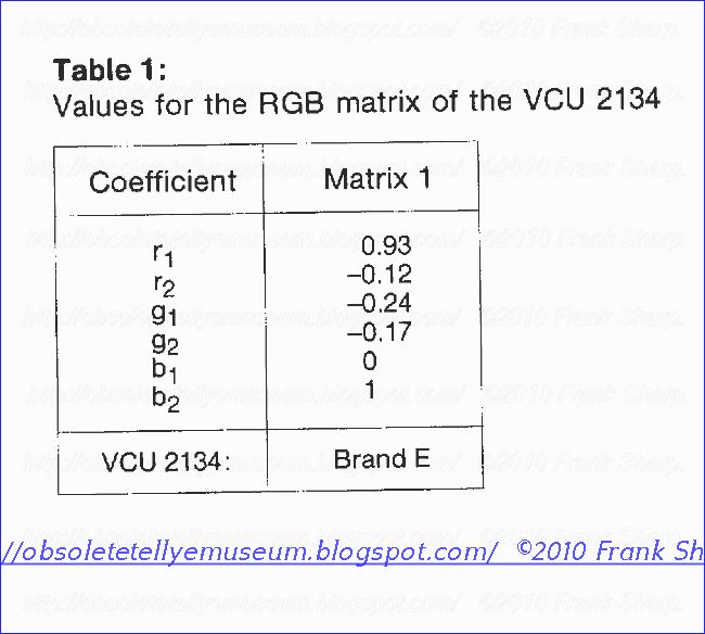
Address no. 16, high byte, bit 6=0 Address no. 16, high byte, bit 5=1: "VHS" mode. Amplification during color burst key x 2 Pin 35: Analog Composite Video, 1.0V max. Pin 37: Analog Composite Video, 1.0V max. Only the data on pin 37 is processed in this mode. Note: The VCU 2136 does not contain the noise inverter that was incorporated in the VCU 2133 any longer. Address no. 16, high byte bit 6 is the former bit "noise inverter”. Changes from the VPU 2203 to the VPU 2204: - on the input side, a demultiplexer was inserted to separate the luma and chroma data in the double data stream and to distribute them into the luma and chroma channels of the VPU (see fig. 3). — the colour trap was conceived to be switched off for the S-VHS operation mode. — Two additional control bits were introduced (refer to the VPU 2203/1E data sheet table 3: "Data transfer between ...”), that is: Address no. 15, low byte, bit 2 "S-VHS on” (see fig. 2): bit 2=0: S-VHS off VPU works on the V1 data only. Luma and chroma data are
separated with the help of chroma trap and chroma filter. bit 2=1: S-VHS on demultiplex of the sequential luma and chroma data, no chroma x 2 during color burst. Address no. 15., low byte, bit 1 (see fig. 3): bit 1=0: chroma trap on. bit 1=1: chroma trap off. New filters in the VPU 2204 To improve frequency response and picture quality some changes in the luminance- and peaking filter part of the VPU have been made. The old filter characteristics are still available. New features are: the S-VHS characteristics without chroma trap the “enhanced” Munakami filter without ringing the “broad” version. For SECAM the broader chroma trap can be switched off to the same chroma trap as for PAL.
DPU 2553, DPU 2554, DPU 2555 Deflection Processors.
During the past few years, digital circuit technology has come into se in television receivers, including color television receivers, for processing the received signal and for generating the deflection signal required to control the movement of the electron beam. During the research for and the development and implementation of these digital circuit systems, the course traced ou by conventional analog signal processing was followed, and the known individual problems were solved by means of digital rather than analog circuits.
By contrast, the present invention is predicated on the realization that, against the background of digital signal processing in television receivers, the constraints resulting from conventional analog technology, particularly with respect to predetermined signal waveforms, can be eliminated, thus making it possible to cope with difficult problems better than with conventional analog and/or digital technology. One of those difficult problems is still the geometric distortions introducted by the nonspherical curvature of the tube screen during reproduction. To eliminate these distortions, a considerable amount of circuitry is required both with conventional analog technology and more recent digital technology; an example is the great number of pincushion-correcting circuits.The fundamental idea of the invention as claimed is to abandon the rigid dependence on the commonly used sawtooth signal for ohorizontal deflection and vertical deflection, which both have a very short retrace period in comparison with the trace period, and to make the individual pixels of the video signal visible on the screen when the two deflection signals have moved the electron beam to the point intended on the transmitter side.
In the present invention, therefore, the deflection signals are no longer generated by a sawtooth generator of long-known analog or more recent digital design, but a deflection processor is provided which generates horizontal and vertical deflection signals with freely selectable waveforms.
The video signal, after being digitized by means of a clock signal, is written into a random-access memory and is read ou in such a way that the individual pixels occupy the intended positions on the screen. The memory has a suitable controller associated therewith, of course. The digital signals read out of the memory must be applied to a compensating stage for correcting picture tube errors before they drive the picture tube via digital-to-analog converters.
Deflection Processors
1.
Introduction These programmable VLSI circuits in N-channel MOS
technology carry out the deflection functions in digital color TV
receivers based on the DIGIT 2000 system and are also suitable for text
and D2-MAC application. The three types are basically identical, but are
modified according to the in- tended application: DPU 2553 —
normal-scan horizontal deflection, standard CTV receivers, also equipped
with Teletext and D2-MAC facility

DPU 2554 -— double-scan horizontal deflection, for CTV receivers equipped with double-frequency horizontal deflection and double-frequency vertical deflection for improved picture quality. At pow- er-up, this version starts with double horizontal frequency.
DPU 2555 — normal scan horizontal deflection as DPU 2553, but with an extra flag for the IM bus, so that one DPU 2553 and one DPU 2555 may be operated simultaneously in one CTV receiver as is required for Teletext or Viewdata operation if increased deflection frequency is intended for high-quality text display. In this case, the DPU 2553 acts as sync separator for the received Teletext or Viewdata signal, whereas the DPU 2555 is used as deflection processor for the displayed page, or viceversa.
1.1.
General Description The DPU 2553/54/55 Deflection Processors contain
the following circuit functions on one single silicon chip: video
clamping horizontal and vertical sync separation horizontal
synchronization normal horizontal deflection east-west correction, also
for flat-screen picture tubes vertical synchronization normal vertical
deflection sawtooth generation text display mode with increased
deflection frequencies (18.7 kHz horizontal and 60 Hz vertical) — D2-MAC
operation mode and for DPU 2554 only: -— double-scan horizontal
deflection - normal and double-scan vertical deflection In this data
sheet, all information given for double-scan mode is available with the
DPU 2554 only.
Types DPU 2553 and DPU 2555 start the horizontal
deflection with 15.5 kHz according to the normal TV standard, whereas
type DPU 2554 starts with 31 KHz according to the double-scan sys- tem.
The
only difference between types DPU 2553 and DPU 2555 is in the function
of the flag IMS which enables and disables the IM bus interface of the
respective deflection processor. With this, it is possible to operate
both types in parallel on the same IM bus, as is required for the
Teletext or Viewdata display mode with increased deflection frequencies.
The following characteristics are programmable: ~ selection of the TV
standard (PAL, D2-MAC or NTSC) - selection of the deflection standard
(Teletext, horizontal and vertical double -scan, and normal scan) —
filter time-constant for horizontal synchronization — vertical
amplitude, S correction, and vertical position for in-line, flat-screen
and Trinitron picture tubes — east-west parabola, horizontal width, and
trapezoidal correction for in-line, flat-screen and Trinitron picture
tubes — switch over characteristics between the different
synchronization modes — characteristic of the synchronism detector for
PLL switching and muting.
1.2. Environment
Fig. 1-1 shows the
simplified block diagram of the video and deflection section of a
digital TV receiver based on the DIGIT 2000 system. The analog video
signal derived from the video detector is digitized in the VCU 2133
Video Codec and supplied in a parallel 7 bit Gray code. This digital
video signal is fed to the video section (VPU, CVPU, SPU and DMA) and to
the DPU 2553/54/55 Deflection Processor which carries out all functions
required in conjunction with deflection, from sync separation to the
control of the deflection power stages, as described in this data sheet.
. Pin Connections

- Ground
- @TMM Main Clock Input
- Output for Single-Scan Vertical Blanking Pulse
- Clamping Output 2
- Reset Input
- Input for the D2-MAC Composite Sync Signal and Output for the Separated Composite Sync Signal
- 1H and 2H Skew Data Output
- Vsup Supply Voltage
- V6 Video Input (MSB)
- V5 Video Input
- V4 Video Input
- V3 Video Input
- V2 Video Input
- V1 Video Input
- VO Video Input (LSB)
- IM Bus Clock Input
- IM Bus Ident Input
- IM Bus Data Input/Output
- Combined Output for the Color Key Pulse and the Undelayed Horizontal Blanking Pulse
- Ground
- Clamping Output 1
- Combined Output for the Delayed Horizontal Blanking Pulse and the Vertical Blanking Pulse
- Horizontal Flyback Input
- Undelayed Horizontal Blanking Output
- Vertical Flyback Safety Input
- Vertical Flyback Output
- Vertical Sawtooth Output
- East-West Parabola Output
- Horizontal Output Polarity Select Input and Start Oscillator Pulsewidth Select Input
- Ground
- Horizontal Output
- Vsup Supply Voltage
- External Standard Selection Input
- Start Oscillator Clock Input
- Start Oscillator Supply Voltage
- Start Oscillator Select Input
- Control Switch Output for the Horizontal Power Stage
- Test Pin, leave vacant
- Interlace Control Output
- Vsup Supply Voltage

2.3. Pin Descriptions
Pins 1, 20 and 30 — Ground These pins must be connected to the negative of the supply.
Pins 2— @M Main Clock Input (Fig. 2-4) By means of this input, the DPU receives the required main clock signal from the MCU 2600 or MCU 2632 Clock Gen- erator IC.
Pin 3 — Single-Scan Vertical Blanking Output (Fig. 2-11) In vertical double-scan mode, this pulse is also required by the CVPU 2235 Comb Filter Video Processor.
Pins 4 and 21 — Clamping Outputs 2 and 1 (Fig. 2-10) These pins supply pulses for clamping the video signal at the VCU 2133 or VCU 2134 during the back porch.
Pin 5 — Reset Input (Fig. 2-2) This pin is used for hardware reset. At low level, reset is actuated, and at high level the DPU is ready for communication with the CCU via the IM bus.
Pin 6 — Input for the D2-MAC Composite Sync Signal and Output for the Separated Composite Sync Signal This pin (Fig. 2-9) is the input for the D2-MAC composite sine signal and the output for the separated composite sync signal.
Pin 7 — Skew Data Output (Fig. 2-10) This pin delivers the 1H and 2H skew data stream required by the PSP 2210 or PSP 2032 Progressive Scan Processor and the TPU 2732 or TPU 2733 or TPU 2740 Teletext Processor or others for adjusting the phase of the double- scan video signal and for information about vertical sync.
Pins 8, 32 and 40 — Vsyp Supply Voltage These pins must be connected to the positive of the supply.
Pins 9 to 15 — V6 to VO Video Inputs (Fig. 2-3) Via these pins, the DPU receives the digitized composite video signal from the VCU 2133 or VCU 2134 Video Codec in a parallel 7-bit Gray code. With a standard signal, the sync pulse resolution is 6 bits.
Pins 16 to 18 — IM Bus Connections These pins connect the DPU to the IM bus. It is via the IM bus that the DPU communicates with the CCU. Pins 16 (IM Bus Clock Input) and 17 (IM Bus Ident Input) have the con- figuration shown in Fig. 2-2. Pin 18 (IM Bus Data Input/Out- put) is shown in Fig. 2-9.
Pin 19 — Combined Output for the Color Key Pulse and the Undelayed Horizontal Blanking Pulse (Fig. 2-11) his output is tristate-controlled. In conjunction with the in- put load represented by the VCU, the three-level key and blanking pulse is produced which is also needed by the other DIGIT 2000 processors.
Pin 22 - Combined Output for the Delayed Horizontal Blanking Pulse and the Vertical Blanking Pulse (Fig. 2-11) This pin is a tristate-controlled output. In conjunction with the input load represented by the VCU, the three-level combined blanking pulse is produced which is also needed by the other DIGIT 2000 processors. Pin 23 — Horizontal Flyback Input (Fig. 2-5) Pin 23 requires horizontal flyback pulses which must be clamped by a diode to the +5 V supply.
Pin 24 — Undelayed Horizontal Blanking Output (Fig. 2-11) This output supplies undelayed horizontal blanking pulses. These pulses are for keying of the IF amplifier and are key- ing pulses for the VCU.
Pin 25 — Vertical Flyback Safety Input (Fig. 2-5) To protect the picture tube from damage by burn-in in the event of a malfunction of the vertical deflection, an ac- knowledge pulse derived from the vertical deflection yoke is fed to pin 25. If this pulse exceeds the 2.5 V threshold during vertical blanking, the blanking pulse will be terminated. If it is planned to operate without this picture tube protection, pin 25 must be connected to +5V.
Pin 26 — Vertical Flyback Output (Fig. 2-12) This pin supplies the same pulse width-modulated sawtooth signal as pin 27, but only for 350 us from the start of the vertical flyback. During the remaining time, pin 26 is at high impedance. The signal supplied by pin 26 is used for fast charge-reversal of the integration capacitor.
Pin 27 ~ Vertical Sawtooth Output (Fig. 2-12) This pin supplies the signal, in pulse width-modulated form, for driving the vertical output stage. To produce the analog sawtooth signal, this signal must be integrated externally, e. g. by an RC network. By way of the IM bus interface and the HSP processor, it is possible for this sawtooth to be varied by the CCU.
Pin 28 — East-West Parabola Output (Fig. 2-12) This pin supplies the vertical-frequency parabola signal for the east-west correction in pulse width-modulated form. Via the IM bus and the HSP processor, the east-west parabola can be adjusted by the CCU.
Pin 29 — Horizontal Output Polarity and Pulse width Select Input (Fig. 2-6) This pin serves for selecting the polarity and the pulse width of the output pulses of pin 31 as described in section 3.4. This pin must be connected to ground or to +5 V.
Pin 31 — Horizontal Output (Fig. 2-10) This output supplies the driving pulses for the horizontal output stage. The output pulse polarity can be selected by means of pin 29.
Pin 33 — External Standard Selection Input (Fig. 2-7) This input is used for selecting the horizontal frequency standard, as shown in Table 3-2. If pin 33 is +5 V, the DPU operates only with the NTSC standard. If it is connected to ground, however, the DPU is set for the PAL or SECAM standard, and the horizontal standard can only be changed by the CCU command between PAL/SECAM and Text dis- play mode. If pin 33 is unconnected, all standards can be selected by the CCU via the IM bus. Furthermore, when pin 33 is unconnected, the horizontal protection circuit is in ef- fect, and for this a 4 MHz signal is required at pin 34. In this case, the output pulse at pin 31 is limited to a maximum du- ration of 30 us for all standards. The phase resolution of the trailing edge of this pulse is reduced to 250 ns, if the output pulse is set to more than 30 ys pulse width.
Pin 34 — Protection Circuit Clock Input (Fig. 2-8) When pin 33 is left unconnected, a 4 MHz clock signal is required at pin 34 for the horizontal protection circuit. The 4 MHz clock can be fed to pin 34 via a capacitor, and is available, e. g., at pin 1 of the CCU at no added cost. If the 4 MHz signal is not present and pin 33 is not connected, the horizontal output pin 31 is undefined.
Pin 35 — Start Oscillator Supply
Via this pin it is possible with minimum current consumption to operate the horizontal protection circuit as a starting oscillator. For this purpose only the 4 MHz signal at pin 34 is required. Pin 36 must be connected to pin 35.
Pin 36 — Start Oscillator Select Input (Fig. 2-6) if the start oscillator function is required (see Table 3-2), pin 36 must be connected to pin 35. If the start oscillator function is not used, pin 36 has to be connected to ground. In this mode, the horizontal output pin 31 is switched off (at high level) as long as the Reset input pin 5 is Low.
Pin 37 — Control Switch Output for the Horizontal Power Stage (Fig. 2-11) This pin serves for switching over the horizontal output
stage to another frequency.
Pin 38 — Test pin This pin is an input/output of the type shown in Fig. 2-9. It is used for testing the DPU during production and should be left unconnected in normal operation.
Pin 39 — Interlace Control Output (Fig. 2-10) This pin is for controlling an AC coupled vertical power stage for interlace-free mode.
3. Functional Description
3.1. Block Diagram
 The
DPU 2553, DPU 2554 and DPU 2555 Deflection Processors perform all tasks
associated with deflection in TV sets: — sync separation — generation
and synchronization of the horizontal and the vertical deflection
frequencies — the various east-west corrections, - vertical sawtooth
generation including S correction as described hereafter. The DPU
communicates, via the bidirectional serial IM bus, with the CCU 2030,
CCU 2050 or CCU 2070 Central Control Unit and, via this bus, is supplied
with the picture-correction alignment information stored in the MDA
2062 EEPROM during set production, when the set is turned on. The DPU is
normally clocked with a trapezoidal 17.734 MHz (PAL or SECAM), or 14.3
MHz (NTSC) or 20.25 MHz (D2-MAC) clock signal supplied by the MCU 2600
or MCU 2632 Clock Generator IC. The functional diagram of the DPU is
shown in Fig. 3-1. 3.2.
The Video Clamping Circuit and the Sync Pulse Separation Circuit The
digitized composite video signal delivered as a 7-bit parallel signal by
the VCU 2133 or
The
DPU 2553, DPU 2554 and DPU 2555 Deflection Processors perform all tasks
associated with deflection in TV sets: — sync separation — generation
and synchronization of the horizontal and the vertical deflection
frequencies — the various east-west corrections, - vertical sawtooth
generation including S correction as described hereafter. The DPU
communicates, via the bidirectional serial IM bus, with the CCU 2030,
CCU 2050 or CCU 2070 Central Control Unit and, via this bus, is supplied
with the picture-correction alignment information stored in the MDA
2062 EEPROM during set production, when the set is turned on. The DPU is
normally clocked with a trapezoidal 17.734 MHz (PAL or SECAM), or 14.3
MHz (NTSC) or 20.25 MHz (D2-MAC) clock signal supplied by the MCU 2600
or MCU 2632 Clock Generator IC. The functional diagram of the DPU is
shown in Fig. 3-1. 3.2.
The Video Clamping Circuit and the Sync Pulse Separation Circuit The
digitized composite video signal delivered as a 7-bit parallel signal by
the VCU 2133 or The DPU has two different clamping outputs, No. 1 and No. 2, one of which supplies the required clamping pulses to the video input of the VCU as shown in Fig. 3-1. The following values for the clamping circuit apply for Video Amp. I. Since the gain of Video Amp. Il is twice that of Video Amp I, all clamping and signal levels of Video Amp II are half those of Video Amp | referred to +5 V. After the TV set is switched on, the video clamping circuit first of all ensures by means of horizontal-frequency cur- rent pulses from the clamping output of the DPU to the coupling capacitor of the analog composite video signal, that the video signal at the VCU’s input is optimally biased for the operation range of the A/D converter of 5 to 7 V. For this, the sync top level is digitally measured and set to a constant level of 5.125 V by these current pulses. The horizontal and vertical sync pulses are now separated by a fixed separation level of 5.250 V so that the horizontal synchronization can lock to the correct phase (
see section 3.3. and Figs. 2-17 and 3-2). With the color key pulse which is now present in synchro with the composite video signal, the video clamping circuit measures the DC voltage level of the porch and by means of the pulses from pin 21 (or pin 4), sets the DC level of the porch at a constant 5.5 V (5.25 V for Video Amp ll). This level is also the reference black level for the VPU 2203, CVPU 2233 or CVPU 2235 Video Processors. When horizontal synchronization is achieved, the slice level for the sync pulses is set to 50 % of the sync pulse amplitude by averaging sync top and black level. This ensures optimum pulse separation, even with small sync pulse amplitudes (see application notes, section 4.).


SPU 2220 SECAM Chroma Processor
SECAM
Chroma Processor Digital real time signal processor for processing
SECAM video chroma signals in combination with the VPU 2203 Video
Processor which processes the luminance information at the same time.
The SPU 2220 is an N-channel VLSI MOS circuit, housed in a 40-pin Dil
plastic package and contains on a single silicon chip the following
functions: — a code converter — a digital SECAM bell filter — a
switchable IF spectrum compensation filter ~ a digital FM de modulator
with DC offset correction, de emphasis and de multiplexer — a digital
Red-/Blue-line identification - a digital standard recognition circuit —
a color saturation multiplier with multiplexer for the color difference
signals — the IM bus interface circuit which provides the communication
with the CCU 2030, CCU 2050 or CCU 2070 Central Control Unit via the
bidirectional IM bus — chroma outputs (pins 23 to 26) can be disabled by
means of pin 22

1. Functional Description
The SPU 2220 digitally processes the SECAM color signals supplied in digital form as a parallel 7-bit Gray-coded signal by the VCU 2133 Video Codec. Acting in parallel with the VPU 2203 Video Processor (Fig. 2),


the SPU 2220 separates the color information from the digital video signal, performs the bell filter function and the IF spectral compensation before submitting the 17.734 MHz sampled signal to the digital algebraic demodulator. The demodulator produces an 8-bit signal, sampled at 4.43 MHz, whose amplitude is proportional to the frequency of the incoming frequency-modulated color difference signal. After demodulation, the color difference signals undergo digital deemphasis before being demultiplexed using a 64 us delay line. After passing the saturation multiplier the co- lor difference signals are multiplexed in a form compatible to that used in the VPU 2203. The SPU 2220 also includes automatic SECAM identification logic as well as Red-/Blue-Line detection and synchronization. Since the signal-
processing delay in the performance of SECAM decoding is greater than that experienced during PAL or NTSC decoding, the SPU 2220 compensates for this delay by delaying the digital video signal supplied to the VPU 2203 by a corresponding amount (5.5 us) in SECAM operation.
1.1. The Code Converter The 7-bit digital video signal supplied by the VCU 2133 Video Codec in the Gray code is initially converted into 7-bit two’s complement binary code for further processing.
1.2. The 5.5 us Delay Line This part of the SPU 2220 delays the digital video signal supplied by the VCU 2133 to be delivered to the VPU 2203. In this way the difference in processing time between the VPU 2203 (luminance channel) and the SPU 2220 (chrominance channel) in SECAM operation is compensated. The color key pulse for the VPU 2203 passes the Aux Delay block of the SPU 2220 in order to provide the same delay as for the video signal delayed in the 5.5 us delay line.
1.3. The SECAM Bell Filter This filter which has the same function as the conventional LC bell filter hitherto used, removes the luminance information and compensates the anti-bell response of the transmitter. Center frequency and frequency response of the bell filter are fixed and cannot be altered externally. The response of the SECAM bell filter is shown in Figs. 3 and 4.
1.4. The IF Spectrum Compensation Filter Since the FM color information in the SECAM system covers a range of frequencies from 3.9 to 4.75 MHz (unlike the single frequency with its AM color information in the PAL and NTSC systems), the slight spectral distortion resulting from the tuner and IF section of the TV set should be compensated. For this, the 14-bit output of the bell filter passes the IF spectrum compensation filter which gives a compensating frequency response of about 4 dB/MHz. This filter can be switched on and off by the CCU via the IM bus using address 107 (see Table 2). Fig. 4 shows the various filter responses of the bell and IF compensation filter with the latter switched on and off.
CVPU 2233 NTSC Comb Filter Video Processor
Article "Color Decoding a PCM NTSC Television Signal" by J. P. Rossi,
Jun., 1974, Journal of the SMPTE, vol. 83, No. 6, pp. 489-495.
Article "Digital Television Image
Enhancement" by J. P. Rossi, 1975, Journal of the SMPTE, vol. 84, at pp.
545-551.
Text "Theory and Application of Digital
Signal Processing" by Rabiner and Gold, (Prentice-Hall, 1975), p. 550.
Paper "Nonrecursive Digital Filters with
Coefficients of Powers of Two" by A. Tomozawa, in the IEEE Int'l. Conf.
on Comm., pp. 18D-1 through 18D-5.
Paper "Colour Demodulation of an NTSC
Television Signal Using Digital Filtering Techniques" by A. G. Deczky,
1975 IEEE Int'l. Conf. on Comm., vol. II, pp. 23-6 through 23-11.
U.S. patent application filed Aug. 31, 1981
in the name of H. G. Lewis, Jr., Digital Color Television Signal
Demodulator, Ser. No.: 297,556.
An Approach to the Implementation of Digital
Filters by L. R. Jackson, reprinted from IEEE Trans. Audio
Electroacoust., vol. AU-16, pp. 413-421, Sep. 1968.
W. Weltersbach et al., "Digitale
Videosignalverarbeitung im Farbfernsehempfanger", Fernseh und
Kino-Technik, 35 Jahrgang, Nr. 9, Sep. 1981, pp. 317-323, (with
translation).
T. Fischer, "Digital VLSI Breeds
Next-Generation TV Receivers", Electronics, Aug. 11, 1981, pp. 97-103.
T. Fischer, "Fernsehen Wird Digital",
Elektronik, No. 16, 1981, pp. 27-35, (with translation of pp. 30-31).
ITT Intermetall, A New Dimension-VLSI Digital TV System, Sep. 1981, pp. 1-23.
In a conventional television receiver, all signals are analog-processed. Analog signal processing, however, has the problems at the video stage and thereafter. These problems stem from the general drawbacks of analog signal processing with regard to time-base operation, specifically, incomplete Y/C separation (which causes cross color and dot interference), various types of problems resulting in low picture quality, and low precision of synchronization. Furthermore, from the viewpoints of cost and ease of manufacturing the analog circuit, a hybrid configuration must be employed even if the main circuit comprises an IC. In addition to these disadvantages, many adjustments must be performed.
In order to solve the above problems, it is proposed to process all signals in a digital form from the video stage to the chrominance signal demodulation stage. In such a digital television receiver, various improvements in picture quality should result due to the advantages of digital signal processing.
NTSC Comb Filter Video Processor Digital real-time signal processor for processing the video signals digitized by the VCU 2133 Video Codec Unit in digital color TV receivers according to the NTSC standard.
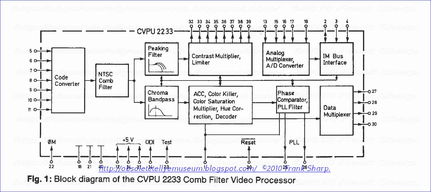
The CVPU 2233 is an N-channel MOS circuit, is housed in a 40- pin Dil plastic package and contains on a single silicon chip the following functions:
— a code converter
— an NTSC comb filter
— the chroma band pass filter
— the luminance filter with peaking facility
— a contrast multiplier with limiter for the luminance signal
~- all color signal processing circuits such as automatic color control (ACC), color killer, identification, decoder and hue correction
~ a color saturation multiplier with multiplexer for the color difference signals
— the IM bus interface circuit for communicating with the CCU 2030 or CCU 2050 Central Control Unit ~ circuitry for measuring dark current (CRT spot-cutoff), white level and photo current, and for transferring this data to the CCU.
1. Functional Description The CVPU 2233 Comb Filter Video Processor digitally processes the digital video signal supplied by the VCU 2133 Video Codec in the various circuit parts just mentioned.


The resulting digital signals are then reconverted to analog signals in the VCU 2133 and used to drive the cathodes of the picture tube, via the external RGB output amplifiers. Further, in conjunction with the VCU 2133, the CVPU 2233 performs a number of measurements and control operations relating to picture tube alignment such as spot-cutoff current adjustment, white level controi, beam current limiting, etc. To understand the signal processing in the two integrated circuits VCU 2133 and CVPU 2233, Fig. 2 may prove useful because it shows the signal flow and the several functional blocks in their logical sequence regardless of whether these blocks are in the VCU 2133 or CVPU 2233.
1.1. The Code Converter This circuit is shown only in Fig. 1. It serves to convert the digitized video signal, delivered by the VCU 2133 in a parallel Gray code, into a simple binary-coded signal for the comb filter.
1.2. The Comb Filter With the NTSC system, a comb filtering for separation of chrominance and luminance signals is easy to realize by a delay line that has the delay of one horizontal period (64 us). In the case of the CVPU 2233, this delay is realized by a RAM. When a comb filter is used, it is no longer necessary to have a chroma trap in the luminance signal path.
1.3. The Luminance Channel The luminance filter has two different values for its band- with, 4 MHz in the case an IF filtered video signal is processed, and 7 MHz if the video signal originates from a camera, a video signal disc player etc. Additionally, the filter handles peaking whereby the high-frequency components of the luminance signal in the range of 3 MHz are raised to improve picture sharpness. The amount of peaking is set by the CCU 2030 or CCU 2050 via the IM bus. Us- ing a fixed subtrahend of —0.25, the sync signal component not required in the luminance channel is suppressed. Peaking at 3 MHz is provided in the range from —3 dB to + 10 dB. It can be set by the user in eight steps. The peaking has a dead-data zone as shown in Fig. 14
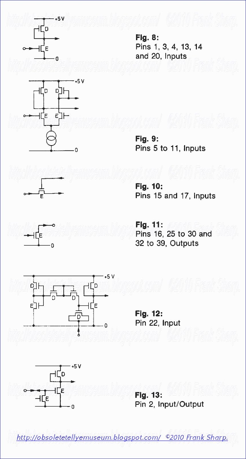
in the description of the VCU 2133. The luminance filter has a DC gain of 1.0 (see Fig. 4). Behind the luminance filter, 9 bits are used to carry the luminance signal, so that the overshoots caused by the peaking filter can be transmitted to the Y D/A converter in
the VCU 2133.
The peaking curves are shown in Fig. 5.
Following the peaking circuit (Fig. 2) is the contrast multiplier which, combined with a limiter, limits the luminance signal if its amplitude becomes too high. The contrast setting, too, is controlled by the CCU via the IM bus, depending on the user’s instructions. Further, the contrast is adapted to the room lighting by means of a photo sensor connected to pin 17 of the CVPU 2233. In this process, the signal generated by the photo sensor is first digitized in the CVPU 2233 and then, during vertical flyback, transferred in multiplex operation to the CCU. The CCU calculates the contrast needed and finally sends the corresponding control signal to the CVPU 2233's contrast multiplier via the IM bus. After the contrast multiplier are added 31 steps as a constant DC signal, so that the system can transmit the negative undershoots-caused by peaking, to the D/A converter (see Fig. 3). From the contrast multiplier, the digital luminance signal is back to 2133 form of a 8-bit signal. In fed the VCU in the VCU 2133,
the signal enters the Y D/A converter. The converter feeds the analog luminance signal to the RGB matrix.
The setting range of the contrast multiplier comprises 6 bits (63 steps) and a gain of 1. If the product of the multiplication at the multiplier’s output is higher than the working range, the largest possible number (1 111 1 1 1 1) is put out. This means the limiting mentioned above is achieved.
4. Inner Configuration of the Connection Pins The following figures schematically show the circuitry at the various pins. The integrated protection structures are not shown. The letter “E” means enhancement, the letter “D” depletion.
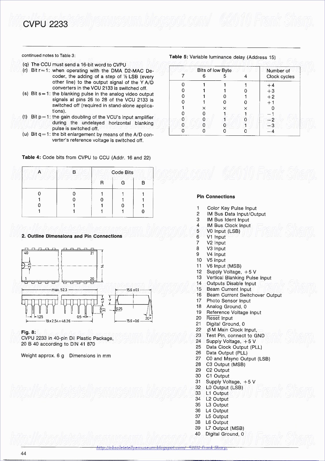

5. Description of the Connections and the Signals
Pin 1 - Color Key Pulse Input This input’s configuration is shown in Fig. 8. Via this pin, the CVPU 2233 gets the color key pulse from pin 19 of the DPU 2543. In the quiescent state high level must be applied, and during pulse a low level.
Pins 2 to 4 - IM Bus Connections By means of these pins, the CVPU 2233 is linked with the CCU 2030 or CCU 2050.
Pins 3 (Ident Input) and 4 (Clock Input) are configured as shown in Fig. 8. Pin 2 (Data Input/ Output) is shown in Fig. 13.
Pins 5 to 11 — Inputs VO to V6 The circuit of these inputs is shown in Fig. 9. Via these in- puts, the CVPU 2233 receives the digitized composite video signal from the VCU 2133 in a 7-bit parallel Gray code. Input VO gets the least significant bit (LSB) and input V6 the most significant bit (MSB).
Pins 12, 24 and 31 — Supply Voltage, +5 V These pins must be connected to the positive of the 5 V supply. Pin 13 — Vertical Blanking Pulse Input Fig. 8 shows the diagram of this input. Via this pin the CVPU 2233 receives the vertical blanking pulse from the DPU 2543. In the steady state, high level must be applied, and during pulse a low level. The vertical blanking pulse is required for controlling the tests described in section 1.5., which are carried out during vertical flyback.
Pin 14 - Outputs Disable Input This input (Fig. 8) serves for fast switch over of the luma and chroma outputs (Pin 27 to 30 and 32 to 39) to the high- impedance state. Pin 14 low means outputs active, and Pin 14 high means outputs disabled.
Pin 15 —- Beam Current Input By means of this pin, whose circuit is shown in Fig. 10, the CVPU 2233 receives the common analog signal which is supplied by three current sensing transistors inserted in the cathode lines of the picture tube. Via the internal switch $1 (Fig. 5) the analog signal is fed to the internal A/D converter. Input voltage range is 0 V to Vig.
Pin 16 — Beam Current Switch over Output This pin serves for selecting the sensitivity of the beam cur- rent input pin 15 by connecting an additional 10 kQ resistor parallel to pin 15 and ground, thus reducing this input’s sensitivity. By this means, the current supplied by the three sensor transistors mentioned is the spot-cutoff current on the one hand (high sensitivity) and the white level current on the other (low sensitivity).
The circuit of pin 16 is shown in Fig. 11.
Pin 17 — Photo Sensor Input This input has the same properties as pin 15. It serves for measuring the current supplied by the photo sensor and is activated by switch S2 (Fig. 5). Its input voltage range is al- so 0 V to Vig.
Pin 18 — Analog Ground, 0 This pin is used as a ground connection in conjunction with pins 15 to 17.
Pin 19 — Reference Voltage Input This pin gets the externally-produced reference voltage of half the supply voltage, that is required by the circuitry shown in Fig. 5 and must be filtered by a capacitor of sufficient capacity.
Pin 20 — Reset Input This pin’s circuit is shown in Fig. 8. In the steady state, high level is required. A low level normalizes the CVPU 2233.
Pins 21 and 40 — Digital Ground, 0 These pins are used as ground connection in all cases where digital signals are invoived.
Pins 22 — gM Main Clock Input Via this pin the CVPU 2233 is supplied with the required main clock signal by the MCU 2600 or MCU 2632 Clock Generator IC. Fig. 12 shows the diagram of Pin 22.
Pin 23 — Test Pin During normal operation, this pin must be connected to ground.
Pin 25 — Data Clock Output (PLL) This pin whose diagram is shown in Fig. 11 supplies the data clock signal needed for the serial data transfer of the PLL information from the phase comparator contained in the CVPU 2233 to the voltage-controlled oscillator (VCO) contained in the MCU 2600 or MCU 2632 Clock Generator IC. The frequency of the data clock signal is one fourth of the main clock’s frequency.
Pin 26 — Data Output (PLL)
This pin whose diagram is shown in Fig. 11 supplies the 12- bit data word explained in section 1.6., which serves for closing the PLL circuit which determines the main clock signal used in the DIGIT 2000 TV receiver.
Pins 27 to 30 — Outputs C3 to CO These outputs’ configuration is shown in Fig. 11. Via these pins, the R-Y, B-Y, and picture tube alignment data is transferred in multiplex operation to the VCU 2133.
Pins 32 to 39 — Outputs LO to L7
These outputs are identical to pin 27, too. Via these pins, the CVPU 2233 delivers the digital luminance signal (Y) to the VCU 2133, where it is reconverted to an analog signal.
VPU 2204
VPU 2204 ,


DTI 2222 2223.
This invention relates generally to digital television systems and specifically to an arrangement for improving the luminance signal transient response characteristics and peaking of a digital television receiver.
A digital television receiver described in the ITT publication entitled "Digit 2000-DSLI Digital TV System," which is incorporated by reference herein, describes a digital color television receiver arrangement having a microprocessor that controls a plurality of function control modules over a so-called IM (Intermetall) bus. The luminance signal processing system of the present invention may be utilized with a television receiver constructed in accordance with the above-mentioned publication.
The art has circuits illustrating transient improvement of video signals to compensate for the effects of limited band-width and the like. In U.S. Pat. No. 4,030,121, issued Jun. 14, 1977, a "video crispener" is disclosed for improving the transient response of vide signals. That system developed first and second differentials of an analog input video signal and processing the first differential through a full wave rectifier and the second differential through a limiting amplifier. The products of the rectifier and limiting amplifier were multiplied and added back to the suitably delayed input video signal. Other variants on the above method were also disclosed. The inventive arrangement of the patent, to Applicants' knowledge has never been implemented in video apparatus.
Peaking of video signals has long been done in television receivers in an attempt to enhance the video display by emphasizing certain frequencies of the video signal. Peaking is arbitrary and is based upon subjective criteria as to what constitutes an optimized display. Conventional analog signal peaking techniques are not useful with digital signals however.
The present invention describes apparatus for processing a digitized luminance signal to accentuate or improve transients in the signal and to selectively and variably peak the signal to emphasize low and high frequencies while controlling undershoot and overshoot of the signal. In accordance with the preferred form of the invention, the various parameters for controlling the amount of peaking and transient improvement are factory settings which may be accomplished in software.
Functional Description 3.1. Block Diagram The DTI 2222 is an N-channel MOS circuit which contains on one silicon chip mainly the following functional blocks (see Fig. 3-1):

- chroma nibble demultiplexer and R-Y/B-Y demultiplexer - R-Y and B-Y interpolation filters - R-Y and B-Y rise time detectors - hold pulse generator - chroma nibble multiplexer - clock generator and MUX/DEMUX control - luminance delay circuit - IM bus interface The normal risetime of Luminance transients is about 150 ns, how- ever, for chrominance transients the rise time is between 800 and 1000 ns. The picture impression, especially of color bars in the standard test pattern, is considerably improved if the chrominance transients are given the same short rise time as the luminance transients.
TPU 2732
Teletext
Processor for Level 1 Teletext The TPU 2732 is specified to handle
Level-1-Teletext information (in Germany: Video text) as it is
transmitted today by the TV broadcast stations in Great Britain, Germany
and other European countries. In this function, the TPU 2732 is part of
the DIGIT 2000 digital TV system and works in con- junction with the
other VLSI circuits and processors of this system. The Teletext adapter
designed with the TPU 2732 is very simple and economic (Fig. 1), so that
this new fea- ture may now become common as it was not possible due to
the high cost of former multi-chip solutions up to now.

The TPU 2732 is an N-channel VLSI MOS circuit, housed in a 40-pin Dil plastic package and contains on a single silicon chip the following functions:
— one-chip solution of the Teletext processing (except for external RAM)
— ghost compensation to eliminate the effects of ghost pictures due to reflections
— as input signal is used the 7-bit digitized composite video signal delivered in a parallel Gray code by the VCU 2133 or VCU 2134 Video Codec
— reduced access time is provided for the Teletext pages by receiving and storing up to eight pages in one go
— up to eight stored pages
— function extended by automatic language-dependent character selection
~ switchover facility PAL/NTSC TPY 2732 H for Hebrew Characters Using the type designation TPU 2732 H, a mask option of the TPU 2732 can be supplied which, instead of the automatic language-dependent character selection described in sections 9.7. and 10.3., only displays the Hebrew character set.
With this device, the language-selecting control bits Cy to C14 or LSO to LS2 have no effect. 1. Short Functional Description The TPU 2732 whose block diagram is shown in Fig. 2, op- erates according to a rigid timing determined by the vertical cycle of the TV receiver. The data acquisition period starts at line 7 with PAL or line 10 with NTSC and ends at line 22 with PAL or line 21 with NTSC. During this period, the input data is processed by a ghost filter which is able to compensate reflections with short delay time of 0 to 0.8 us for PAL or 0 to 1 us for NTSC. Teletext information is synchronized and identified. A comparator pre selects the pages with page numbers that are requested by the CCU 2030, CCU 2050 or CCU 2070 Central Control Unit and loads them into the RAM. To eliminate speed problems of the external RAMs, the data is buffered in an internal RAM buffer (Fig. 2). The comparator contained in the data acquisition unit decides into which sector of the RAM the data is stored. The display period
starts at line 48 with PAL or line 50 with NTSC and ends at line 286 with PAL or line 242 with NTSC. The display control unit selects one of the stored eight pages for display. The 8-bit character words are trans- formed into a 6 x 10 dot matrix with PAL or 6 x 8 dot matrix with NTSC by a character generator (ROM) of 96 programmed characters and are displayed in 24 rows of 40 characters each. Different character sets are available for eight languages under CCU or transmitter control, the required character set being selected automatically by the control bits C1 to C14 of row O of the Teletext page display- ed. Every tenth line with PAL or every eighth line with NTSC a new Teletext row is loaded from the RAM into the RAM buffer. When the RAM is not.accessed by the TPU 2732, the memory control refreshes the memory and handles CCU requests for RAM access. Via the IM bus the CCU can read from and write into ail RAM locations and controls the TPU 2732 by loading the appropriate registers in the RAM, so that the
TPU 2732 can be used to display text from other sources. The TPU 2732 can display a list of contents of the stored eight pages (me- nu) all by itself. As external RAM can be used either one 64 K x 1 bit Dynamic RAM or one 16 K x 1 bit Dynamic RAM. So, the RAM capacity is flexible to store 2 or 8 pages. The RAMs can be standard types (see section 3.).
 MCU 2600 Clock Generator IC
Clock
Generator IC Integrated circuit in Cl technology for generating the
main clock @M for digital TV receivers according to the DIGIT 2000
concept.
1.
Introduction The MCU 2600 Clock Generator IC supplies the digital
signal processors, decoders, converters etc. of the DIGIT 2000 digital
TV system with the required main clock signal, which is of trapezoidal
shape, with rounded corners, in order to avoid interference.
For PAL
and SECAM, the clock frequency is four times the PAL color subcarrier
frequency, and for NTSC, the clock frequency is four times the NTSC
color subcarrier frequency: for PAL and SECAM: fom=4 x 4.4383 618 75
MHz= 17.734475 MHz for NTSC: fom=4 x 3.579545 MHz= 14.318 180 MHz for
D2-MAC: fg. =20.25 MHz
2. Functional Description As can be seen from the block diagram Fig. 2-1,


three VCOs (voltage-controlled oscillators) integrated in the MCU 2600 Clock Generator IC (one for PAL and SECAM, one for NTSC, and one for D2-MAC operation) form part of a PLL (phase-locked loop) circuit, the other parts of which, the phase comparator and the digital PLL filter are placed in the VPU 2203 or the CVPU 2233 or the CVPU 2235 or the DMA 2270. The filtered phase difference signal Ag is sup- plied in digital serial form (Fig. 2-2) to pin 6 of the MCU 2600. This data transfer is controlled by means of the data clock signal which is fed to pin 5 of the MCU 2600 and whose frequency is % of the main clock signal @M. With the negative transition of the data clock signal, the data is written into the shift register, and with the positive transition, the content of the shift register is shifted by 1 bit. After 12 bit have been written into the shift register and the data clock signal has attained again the stable high level (Fig. 2-2), an internal delay of about one data clock period occurs.
This following, the data are taken over into the parallel register. From there, the information is fed to the oscillator control circuit and to the 9-stage D/A converter that produces the tuning voltage for the three voltage-controlled oscillators. The write-and-store cycle is initiated at the begin of each horizontal sweep. The closed control loop ensures a phase-true locking be- tween the oscillator signal (from which is produced the @M main clock) and the color subcarrier burst or the digital data burst contained in the received signal. The signal produced by the VCO in action, is transferred to the filter via the oscillator control circuit. The filter forms the required main clock @M and is followed by the output buffer that provides a low-impedance output signal suited for clocking the DIGIT 2000 signal processors. The timing of the data transfer from the VPU 2203, CVPU 2233 or CVPU 2235 Video Processor or the DMA 2270 D2-- MAC Decoder to the MCU 2600 Clock Generator IC is illustrated in Fig. 2-2. The
first three bits serve for selecting the required VCO, depending on whether PAL/SECAM, NTSC, or D2-MAC operation is chosen. The following nine bits (LSB first) provide the tuning signal for the VCO in the shape of two’s complement. These nine bits are composed of the filtered sign-containing phase deviation Aq (7 bits) and the sign-containing alignment value for the oscillator (8 bits). If the MCU 2600 Clock Generator IC is employed in a multi- standard TV set, the required VCO is selected in the way al- ready described. For use in a single-standard receiver, the selection of the operating VCO is free and independent of the data signal. The not-used oscillators can be blocked externally by applying ground to pins 9, 10 or 12. In the case of a multi-standard TV set with up to three operated VCOs, the priority level for operation is internally fixed with the highest level for VCO 1 and the lowest level for VCO 3. This means, when switching on and also in the case of data faults the oscillator control circuit
will select the oscillator with the highest level, if the input of this oscillator is not externally grounded. It should be noted that all connection rails on the PC board must be designed under the point of view of HF signals. An inductance of 10 nH/cm can be assumed at a 0.5 to 1 mm wide rail. This makes an inductive impedance of several Ohms per cm length for the important 3°¢ harmonic of f gy. Best performance is given by ground plane layout of the PC board. All ground and signal lines should be as wide as possible, inductance-free and without loops in the neighbourhood of high HF currents. All supply pins of the clock generator IC must be equipped with ceramic bypass capacitors directly at the IC to ground pins on the shortest possible way.
6. Description of the Connections and Signals
Pin 1 — Ground of Output Buffer This pin serves as separate ground pin for the output buffer and must be carefully decoupled from the crystal oscillators and the input signals.
Pin 3 —- @M Main Clock Output (Fig. 5-1) This pin supplies the clock signal for the DIGIT 2000 TV receiver for clocking all signal processors used in this system.
Pin 4 — Vsyp Output Buffer Supply A positive supply voltage of 5 V is required which powers the output buffer and must be well decoupled with respect to the other supply pin. For this, a bypass capacitor is required between pins 4 and 1.
Pin 5 — PLL Clock Input (Fig. 5-2) Via this pin the MCU 2600 Clock Generator receives the PLL clock for transferring the tuning signal from the VPU, the CVPU or the DMA to the VCO integrated in the MCU 2600.
Pin 6 — PLL Data Input (Fig. 5-2) The desired oscillator is selected by the signal fed to pin 6 as described in Table 4-1. Additionally, pin 6 receives the digital PLL information supplied by the VPU, the CVPU or the DMA, to control the VCO included in the MCU 2600 Clock Generator.
Pin 7 — Ground This pin serves as ground pin for the whole circuit except the output buffer. Its connection should be separated care- fully from the pin 1 ground connection.
Pins 8 to 13 — Crystal Connections (Fig. 5-3) In addition to the oscillator function, the respective input pin serves also for switching off the not-used oscillators by connecting their input pins to ground (pin 7).
Pin 14 — Vgyp Supply Voltage This pin is the supply pin for the whole IC except the output buffer. It must be decoupled carefully with respect to the output buffer supply pin 4. For this, a bypass capacitor between pins 14 and 7 is required.
MDA 2062 1024-Bit EEPROM
1024-Bit EEPROM
Electrically erasable programmable read-only memory (EEPROM) in N-channel floating-gate technology with a capacity of 128 words, 8 bits each. The MDA 2062 is intended for use as a re programmable non-volatile memory in conjunction with the CCU 2030/2050/2070 series Central Control Units of the DIGIT 2000 Digital TV System, the MAA 4000 Remote-Control and PLL-Tuning Microcomputers for TV receivers or the SAA 1280, SAA 1290 and SAA 1293 Remote-Control and Tuning ICs. It serves for storing the tuning information as well as several analog settings, further alignment information given in the factory when producing the TV set. The stored information remains stored even with the supply voltages switched off. Reading and programming operations are executed via the IM bus (see section 7.). Input and output signals are TTL level. An address option input provides the possibility to operate two memories in parallel, to obtain a total storage capacity of 2048 bits.

1. Functional Description
1.1. Memory Operation
The internal memory address space ranges from address 128 to address 255. Addresses 4 and 14 provide special functions. To read a stored data word, the desired memory address has to be entered to the memory address register first. This is done by serially entering the IM bus address 128 (optionally 132) (during Ident = L), followed by the memo- ry address (during Ident = H) in a single IM bus operation. With the memory address register set, the memory data may be read. This, in turn, is done by entering the IM bus address 129 (optionally 133) to the device (during Ident = L). Immediately after this, within the same IM bus operation (during Ident = H) the open-drain Data output will conduct to serially transmit the respective 8-bit memory data. Reprogramming a memory location is done in two steps, a) and b), that are identical except for the data word to be entered. Step a) resets all bits to “1”, and step b) programs the desired data into the selected memory location. a) First, the desired memory address is
entered in the way described above. Second, the actual programming is initiated by serially entering the IM bus address 131 (optional- ly 135) followed by the data word to be stored, which is 255 for step a). The device will now internally time its program- ming sequence of approx. 16 periods of the 1 kHz memory clock. During this “busy” time all inputs are blocked from affecting the programming except for the Reset input. A Reset = L signal will immediately cancel any programming operation as well as any bus operation in progress. The busy state may be interrogated by reading bit 1 of ad- dress location 14. A high level of this “busy-bit” indicates that programming is still under way. The IM bus operation for entering address 14 should always directly precede reading the busy-bit. Reading any other address location during the busy state will produce erroneous data at the Data output. An address change operation during the busy state will not change the memory address register content. The intended start of another programming operation during the busy time will not be executed. b) After time-out, normal operation may be resumed, e. g. by performing the second step of a programming sequence, i. e. by programming the desired 8-bit data word into the respective memory address location. This is done by restoring the proper memory address first, if necessary, and then by serially entering the IM bus address 131 (optionally 135) followed by the desired 8-bit data word. The device will again time its own programming sequence as described under a). After time-out the new data may be verified.
1.2. Redundancy
The MDA 2062 EEPROM contains circuitry that allows to replace up to two rows of the memory matrix, each containing 4 bytes of memory, by redundant rows SR 1 and SR 2. This substitution can be done in the field, by the user. To prepare for activation of SR 1, memory address location 192 must contain the 5 LSB of the memory address containing the defect, which identifies the row to be substituted. Furthermore, bit 5 has to be set to “0”, which identifies the data to be redundancy relevant (see Fig. 2). To prepare for activation of SR 2, memory address location 160 must contain the equivalent data.
The activation itself of the redundant rows is done by reading the content of memory address locations 192 and 160. This transfers the repair information stored nonvolately in the memory array to volatile repair registers. It is important to note that the repair registers are cleared (bit 5 set to “1”) by any Reset = L signal. Thus, any LH transition of the Reset signal must immediately be followed by reading the memory address locations 192 and 160, which restores the repair information to the repair registers. SR 2 may be substituted by SR 1, whereas SR 1 cannot be substituted. As well, row 0 which contains the memory address locations 192 and 160 cannot be substituted. SR 1 and SR 2 are part of the memory matrix portion that is not protectable by the S signal. Memory address locations 192 and 160 are part of the protectable portion.
1.3. Testing The MDA 2062 EEPROM contains circuitry designed to facilitate testing of the various functions. By programming data into address location 4, the device is switched to one or more of a number of test modes. A detailed description is given in section 6.
1.4. Protected Matrix The programming matrix contains a protectable portion. Addresses 128 to 134, 160 to 166, 192 to 198 and 224 to 230 can only be programmed if the “Safe” input S (pin 6) is at high potential. In that way, this portion of the memory is protected against inadvertent reprogramming even if such false information were received via the IM bus. The second part of the programming matrix is not protected.
1.5. Shipment Parts are shipped with all bits set to “1”, except for ad- dresses 192 and 160 which may contain repair information. The content of memory address locations 192 and 160, if different from 255, should not be altered, as this will result in defective rows appearing within the memory address space.
5. Description of the Connections and the Signals
Pin 1 — Option Input Fig. 5 shows the internal configuration of this input. With Pin 1 at ground potential (low) or floating, the MDA 2062 reacts upon the IM bus addresses 128, 129 and 131. With pin 1 continuously at Vpp potential (high), the MDA 2062 reacts upon this IM bus addresses 132, 133 and 135 (see Fig. 8). In this way, parallel operation of two MDA 2062 is permitted, to obtain 2048 bits of non-volatile storage direct- ly accessible via the IM bus. Pin 1 is internally tied to ground via a transistor equivalent to a 40 kQ resistor.


Pins 2, 4, 5 and 11 — NC These pins are not connected internally.
Pin 3 — Programming Voltage Vp A programming voltage of + 20 V (+ 5%) is required. The current consumption during programming is approximately 1 mA. During non-programming operations, pin 3 may be held at any level between (Vpp — 0.7 V) and + 21 V. It may also be left floating. The MDA 2062 EEPROM must not be inserted or removed from a socket with Vp > 6 V. During power on/off sequences, current from the Vp supply should be limited to Ip max = 5 MA.
Pin 6 ~ Safe Input S Fig. 5 shows the internal configuration of this input. Normally, with pin 6 at ground potential (low), one portion of the programming matrix is protected so that this part of the memory cannot be reprogrammed inadvertently. Only when pin 6 receives high potential continuously, the protected portion of the memory matrix can be programmed. Pin 6 is internally tied to ground via a transistor equivalent to a 40 kQ. resistor.
Pin 7 — Ground, 0 This pin must be connected to the negative of the supplies.
Pins 8 to 10 — IM Bus Connections These pins serve to connect the MDA 2062 EEPROM to the IM bus (see section 7.), via which it communicates with the CCU 2030/2050/2070 or MAA 4030 series pC or the SAA 1280/SAA 1290/SAA 1293.
Pins 8 (IM Bus Clock In- put) and 9 (IM Bus Ident Input) are inputs as shown in Fig. 6 and pin 10 (IM Bus Data) is an input/output as shown in Fig. 7. The signal diagram for the IM bus is illustrated in Figs. 8 and 11. The required addresses which the MDA 2062 EEPROM receives from the microcomputer, are also shown in Fig. 8.

Pin 12 — Reset Input This input has a configuration as shown in Fig. 6. Via this in- put, the MDA 2062, together with the other circuits belong- ing to the system, receives the Reset signal which is derived from Vpp via an external RC circuit. A low level is required during power-up and power-down procedures. Low level at pin 12 (max. 1.3 V) cancels a programming procedure and an IM bus operation in progress.
The memory address register is not, the repair register is erased.
During operation, pin 12 requires high level (min. 2.4 V). Pin 13 — Memory Clock Input Via this input (Fig. 6) the MDA 2062 receives a 1 kHz clock signal from pin 3 of the CCU 2030, CCU 2050, CCU 2070 or MAA 4030 microcomputer or the SAA 1280/SAA 1290/SAA 1293.
Pin 14 — Supply Voltage Vpp
The supply voltage required is + 5 V (+ 5 %), and the current
consumption in active operation is approx. 30 mA.
6. Test Functions
This description of the test byte is not part of the specification. It contains no information necessary for normal (intended) use of the MDA 2062 memory. It is only intended as a description of the various functions of the test byte that are designed for factory use, but it does not specify such properties. The description is subject to change. Address location 4 contains a test byte which governs test mode operation of the MDA 2062. The test byte is set by performing the IM bus operation for entering address 4, followed by an IM bus programming operation with the desired test data word.
The test byte is valid during all following IM bus operations until changed or set to 0 by a Reset = L signal. The test byte shall not be changed during the busy time of a programming operation. Fig. 9 shows the bit arrangement of the test byte. Set bit 5 for activation of the test byte!
Block Programming Three block program modes can be activated by the test byte, in conjunction with the memory address loaded into the memory address register: 1) all bytes are selected (including 8 bytes in redundant rows): 2) all even-numbered bytes are selected (redundant bytes are not predetermined, they have to be defined as even bytes): 3) all odd-numbered bytes are selected (redundant bytes are not predetermined): memory address 76543210 1xxxxxOx (e.g. 128) 1xxxxx10 = (e.g. 130) 1xxxxx11~= (e.g. 131)
Thus, programming all selected bytes with the same de- sired data is done within one programming sequence. The complete sequence is: Enter Address 4 Program Test byte (e. g. 160) Enter Address 128, 130 or 131 Program Data A checker board pattern is programmed with two program- ming operations after loading the test byte: Enter Address 130 Program Data 85 Enter Address 131 Program Data 170 Read Reference Shifting
During read operations the memory cell threshold voltage is compared with a reference voltage. The comparator out- put then produces the logic one level for a cell threshold higher than the reference and the logic zero level for a cell threshold lower than the reference. The test byte provides means to shift the reference voltage in positive or negative direction in three steps: +0.3V, +06Vand + 09V.
During a read operation a positive-shifted reference voltage establishes a margin test for logic ones, whereas a negative-shifted reference does so for logic zeroes. This margin test is performed digitally by IM bus operations on- ly, without the need to switch analog power supplies. +0.9V: +0.6V: +0.3V: -—-03V: —06V: —~0O9V: 76543210 ~x010x1x1 x010x0x1 x010x1x0 *x110x0x0 x011x0x0 ‘%~111x0x0
Redundancy Disable
With bit one of the test byte set, the redundant rows can be accessed neither during byte program operations nor during any read operation, even if the redundancy registers are properly loaded. This test byte function has no effect on block programming operations.
Ramp Disable
The MDA 2062 contains circuitry to shape the internal program supply voltage to be a ramp function during programming operations. This feature is considered to be essential to a high erase/write endurance of the memory cells. Bit 3 of the test byte disables this ramp function so that the internal program supply, according to the timing diagram Fig. 10, is immediately disconnected from the Vop supply and connected to the Vp supply at the 4th falling edge of the 1 kHz memory clock, and is immediately disconnected from the Vp supply and re-connected to the Vpp supply at the 14th falling edge of the 1 kHz clock after the last rising Ident signal edge of the IM bus operation starting the program cycle. By this feature other than the built-in ramp function (approx. 100 ts/V) can be applied via the Vp supply pin.
7. Description of the IM Bus
The INTERMETALL Bus (IM Bus for short) has been designed to control the DIGIT 2000 ICs by the CCU Central Control Unit. Via this bus the CCU can write data to the ICs or read data from them. This means the CCU acts as a master whereas all controlled ICs are slaves. The IM Bus consists of three lines for the signals Ident (ID), Clock (CL) and Data (D). The clock frequency range is 50 Hz to 170 KHz. Ident and clock are unidirectional from the CCU to the slave ICs, Data is bidirectional. Bidirectionality is achieved by using open-drain outputs with On-resistances of 150 2 maximum. The 2.5 kQ pull-up resistor common to all outputs is incorporated in the CCU. The timing of a complete IM Bus transaction is shown in Fig. 11 and Table 1. In the non-operative state the signals of all three bus lines are High. To start a transaction the CCU sets the ID signal to Low level, indicating an address transmission, and sets the CL signal to Low level as well to switch the first bit on the Data line. Thereafter eight address

bits are transmitted beginning with the LSB. Data takeover in the slave ICs occurs at the High levels of the clock signal. At the end of the address byte the ID signal goes High, initiating the address comparison in the slave circuits. In the addressed slave the IM bus interface switches over to Data read or write, because these functions are correlated to the address. Also controlled by the address the CCU now transmits eight or sixteen clock pulses, and accordingly one or two bytes of data are written into the addressed IC or read out from it, beginning with the LSB. The Low clock level after the last clock pulse switches the Data line to High level. After this the completion of the bus transaction is signalled by a short Low state pulse of the ID signal. This initiates the storing of the transferred data. It is permissible to interrupt a bus transaction for up to 10 ms.
ADC 2310 E Audio A/D Converter
Audio A/D Converter
1. Introduction
Analog-to-digital
converter for digitizing the analog stereo sound signals in digital TV
receivers based on the DIGIT 2000 system, intended for working together
with the APU 2400 T or the APU 2470 Audio Processor, being controlled by
the CCU 2030, CCU 2050 or CCU 2070 Central Control Unit and being
clocked by the MCU 2632 Clock Generator. The ADC 2310 E is an integrated
circuit in Cl technology, housed in a 24-pin Dil plastic package, and
contains on one silicon chip the following functions (see Fig. 1-1):

— several analog input and output amplifiers
— five analog switches (S1 to $5) for selecting different
signal sources
— an analog stereo dematrix circuit
— alevel control facility
- two pulse-density modulators (PDM | and PDM Il)
— an IM bus interface
2. Functional Description Fig. 2-1 shows the block diagram of a digital stereo sound channel intended for a DIGIT 2000 TV receiver, equipped with additional audio inputs and outputs which can be used with the so-called Euro connector or SCART connector, e. g. for connecting a video recorder.
The analog sound signals selected for conversion by the analog switch S1 firstly pass through the level control section where the desired level control is carried out. Thereafter, they are fed to the first processing stage of the A/D conversion, the pulse-density modulators PDM | and PDM Il, whose output signals are 1-bit data streams with a data rate of 4.7 MHz maximum. This data is then transferred to the APU Audio Processor where the digital decimation filters are the input, performing the second step of the con- version process. Due to the very high sampling rate of the pulse-density modulators, no steep anti-aliasing filters are needed at the input. The digital output data of the whole converting system has a signal-to-noise ratio which can be compared to that of a conventional 13-bit A/D converter.
The TV Audio inputs get their analog signal (_+R and 2 R) from the stereo decoder of the TV set, whereas the Aux. Analog inputs are intended to receive an audio signal from a video recorder or another external source, e.g. via the SCART connector. The Analog Out | and II pins supply the selected audio signal, e.g., to the SCART connector for connection to a video recorder or other equipment.
2.1. The Analog Switches The five analog switches S1 to S5 (S1 and S3 are two-pole switches) are controlled via the IM bus (see section 2.6.) to select the required connections between the four analog inputs and the two digital outputs and the two additional analog outputs.
2.2. The Dematrix When switched on via the IM bus (switch 2, see Table 2-2),


the dematrix provides the 2 R and 2L stereo signals at the analog outputs. These signals are extracted form the L+R and 2R input signals according to the German TV stereo sound system (see Table 2-1 ).
2.3. The Pulse-Density Modulators The two pulse-density modulators, PDM | and PDM Il, are sigma-delta modulators equipped with two feedback loops each. At the outputs they supply pulse trains whose pulse density is proportional to the amplitude of the input signal. The maximum sampling rate, and thus the maximum pulse rate, is 4.7 MHz. possibilities are switched off, the capacitor at pin 9 is discharged rapidly to 2.8 V, and the level control goes to full level. The level control is under IM Bus control as shown in Table 2-2.
2.4. The Level Control Section This part of the ADC 2310 E serves to reduce the level of the input signal to be converted if the input signal exceeds the level for full drive of the PDM pulse-density modulators. Controlled by the IM bus, the audio level is sensed either in channel | or in channel fl or in both channels. If all three possibilities are switched off, the capacitor at pin 9 is discharged rapidly to 2.8 V, and the level control goes to full level. The level control is under IM Bus control as shown in Table 2-2.
2.5. The Clock Divider This part of the ADC 2310 E is provided for adapting the digital stereo sound channel to different TV standards. With bit 7 = Low (see Table 2-2 ), the divider ratio is set to 4:1, whereas bit 7 = High gives 3:1. This allows operation of the ADC 2310 E with almost the same sampling frequency at a main clock frequency OM of 17.7 MHz (PAL) or 14.3 MHz (NTSC), both supplied by the MCU 2632 Clock Generator.
2.6. The IM Bus Interface This circuit section is provided for controlling the ADC 2310 E by the CCU 2030, CCU 2050 or CCU 2070 Central Control Unit via the IM bus (see section 7.). In the case of ADC 2310 E, the IM bus is unidirectional from the CCU to the ADC. That means that information is only transferred from the CCU to the ADC 2310 E. The bit arrangement is shown in Fig. 2-2, and the actions performed can be de- rived from Table 2-2.
2.7. The Preemphasis and Deemphasis
The audio signal supplied by the stereo decoder or video demodulator of the TV set has a preemphasis determined.
5. Description of the Connections and Signals
Pin 1 — Ground
(Analog) This pin serves as ground connection for the analog input signals at pins 4, 5, 8, 21 and 24 and as ground connection for the supply of the analog part of the ADC 2310 E.
Pins 2, 3, 6 and 7 — Capacitor Pins (Fig. 4-8) The filter capacitors for the inner and the outer feedback loop of the pulse-density modulators PDM | and PDM II must be connected to these pins.
Pins 4 and 5 — Analog (TV) Audio Inputs | and I! (Fig. 4-1)


These two inputs get their input signal from the stereo decoder or sound demodulator of the TV set, coupled via capacitors. The input signal range can be increased by adding series resistors.
Pin 8 — Analog (TV) Pilot Input (Fig. 4-2) It is possible to supply the ADC 2310 E with the pilot regardless of the position of switch S1 via this pin. The signal must be coupled capacitively.
Pin 9 ~ Level Control RC Pin (Fig. 4-9) The RC element connected to this pin determines the response time of the level control circuit.
Pins 10 and 11 — PDM Digital Sound Outputs (Fig. 4-5) These pins are the outputs of the pulse-density modulators PDM | and II which supply the PDM data to the APU Audio Processor.
Pin 12 —Vgyp; Supply Voltage (Analog) The analog circuitry of the ADC 2310 E is supplied via this pin.
Pin 13 —- Vgype Supply Voltage The supply at this pin powers the analog switches.
Pin 14 — Ground (Digital)
This pin is the ground connection for the digital output signals supplied by pins 10 and 11 and for the supply of the digital part of the ADC 2310 E.
Pin 15 — @M Clock Input (Fig. 4-3) This pin receives the required clock signal from the MCU 2632 Clock Generator.
Pin 16 — Bit 6 Data Output (Fig. 4-6) This output provides the status of bit 6 (see Table 2-2).
Pins 17 to 19 ~ IM Bus Inputs (Fig. 4-4) The ADC 2310 E is connected to the IM Bus and receives commands issued by the CCU via these pins.
Pin 20 — Vgyp; Supply Voltage (Digital) Pin 20 supplies the digital part of the ADC 2310 E.
Pins 21 and 24 — Analog (Aux) Audio Inputs | and Il (Fig. 4-2) These inputs can be used as playback inputs from a video recorder or other external sources, e. g. connected via the Euro or SCART connector. The input signal must be coupled via capacitors. The input signal range can be in- creased by adding series resistors.
Pins 22 and 23 —- Analog Audio Outputs | and II (Fig. 4-7)
These two analog outputs provide either the signals of the TV inputs (pins 4 and 5) or the signals of the Aux inputs pins 21 and 24, depending on the state of the analog switches which are set by the CCU via the IM bus according to Table 2-2.
APU2470 Audio Processor
digital Audio Processor
1. Introduction
The APU 2470 Audio Processor is an N-channel MOS circuit, housed in a 24 pin Dil plastic package. It is designed to perform digital processing of TV audio information. The architecture of the APU 2
 470 combines two main blocks:
1/0 blocks DSP block The I/O blocks are used to manage the input and output of audio information. The DSP block consists of a mask-programmable digital signal processor, whose software can be controlled by a microprocessor (CCU) via the IM bus. So parameters like coefficients can be modified during performance. By means of the DSP software, audio functions like dematrixing, bilingual mode, tone manipulation and volume control are performed. To allow bilingual performance two audio processing channels are available: MAIN channel, provided for the loudspeaker system AUX channel, provided for headphones Fig. 1-1 gives an overview of the APU functions.
1.1. Application of the APU 2470 The APU2470 is designed to interface with ITT’s ADC 2310E Audio A/D Converter as well as with the DMA 2270 D2-MAC Decoder or the NIP 2400 NICAM Demodulator/Decoder and the AMU 2485 Audio Mixer. It can receive digital data in two different formats:
a) The ADC 2310E receives analog audio information either from the SCART Interface, also called Euro connector (for example: video recorder) or from any terrestrial TV transmission and converts it into two 1-bit PDM streams. For this input format, decimation filters are provided in the APU 2470, converting each PDM stream into a 16-bit word at a sampling rate of approximately 35 kHz.
b) Digital serial audio data, provided for example by the DMA 2270 D2-MAC Decoder or the NIP 2400 NICAM Demodulator/Decoder and mixed in the AMU 2485 Audio Mixer, can be received via the S bus by means of the S bus interface.
ITT’s CCU 2030, CCU 2050, CCU 2070 or CCU 3000 Central Control Units of the DIGIT 2000 family are well suited for interfacing with the APU 2470 Audio Processor. Fig. 1-2 shows how the APU 2470 can be used together with the mentioned ITT ICs to realize multistandard audio processing with PAL and D2-MAC or NICAM signals. In the follow- ing descriptions data coming from the ADC will be called “PDM-Data’”, and data from the AMU will be called “S-Data”. Two different audio configurations are possible with the APU 2470 (Fig. 1-2). The dashed line version uses the AMU 2485 as a pre processing unit both for PDM-Data and S-Da- ta and allows mixing between both kinds of inputs. Another advantage of this version is the digital 50 us deemphasis included in the AMU 2485 applied to the PDM inputs. This gives the flexibility to switch between the D2-MAC/NICAM J17 deemphasis and the FM 50 us deemphasis without using analog means. This version is recommended for new TV concepts. The other application needs an analog 50 us
deemphasis in case of S-Data input in the AMU 2485. For that reason a switchable 50 us preemphasis is included in the AMU 2485. This version can be used in conjunction with the old ADC-APU concept.

5.3. Pin Descriptions
Pins 1 and 21 — Reference Current Inputs (Fig. 5-2) These inputs require a current of 150 uA called reference current Ine- and serving for volume adjustment in the DAC interfaces.
Pins 2 and 12 — Digital Ground, 0 These pins must be connected to the negative of the supply. They have to be used for ground connections in con- junction with digital signals.
Pins 3, 4 and 5 — IM Bus Connections
Via these pins, the APU 2470 is connected to the IM bus and communicates with the CCU. Pins 4 (IM bus Ident input) and 5 (IM bus Clock input) have the configuration shown in Fig. 5-3. Pin 3 (IM bus Data input/output) is shown in Fig. 5-7. The IM bus is described in section 2.1.3.
Pins 6, 8, 9 and 15 — Serial Audio Interface (S Bus)
Pin 9 is the S-Data input (Fig. 5-6) and pin 6 the S-Data out- put (Fig. 5-9). Pins 8 and 15 are S-Clock and S-Ident inputs/outputs (Fig. 5-8), the status depending on bit 4 in co- efficient k33 (see sections 2.1.2. and 4.13.). Pins 7, 14 and 18 — Vsyp Supply Voltage These pins must be connected to the positive of the supply. The clock buffer supply pin 14 must be decoupled carefully from the other supply pins.
Pin 10 — Vigg internal Substrate Bias Voltage
The APU 2470 has an on-chip substrate bias generator which produces a negative bias voltage of about 3.4 V. Pin 10 should have a 0.1 uF capacitor to ground.
Pin 11 — Reset Input (Fig. 5-3)
In the steady state, high level is required at pin 11. A low level normalizes the APU 2470. Initialization of the APU 2470 is described in section 4.12.
Pin 13 — @M
Main Clock Input (Fig. 5-4) This pin receives the required main clock signal from the MCU 2600 or MCU 2632 Clock Generator IC or from the DMA 2270 D2-MAC Decoder or the NIP 2400 NICAM Demodulator/Decoder.
Pins 16 and 17 —- PDM Il and PDM | Digital Inputs (Fig. 5-5) These pins receive the pulse-density modulated output signals of the ADC 2300 E or ADC 2310 E.
Pins 19 and 20 - AUX DAC Outputs 2L and 2R (Fig. 5-9) These pins supply the audio output signals as output cur- rents whose amplitude is determined by the reference cur- rent Inco fed to pin 1. The output signal of pins 19 and 20 is not influenced by the VOL 1 and VOL 2 volume controls and is intended for headphones, for example.
Pins 22 and 23 — MAIN DAC Outputs 1L
and 1R (Fig. 5-9) These pins supply the audio output signals as output cur- rents whose amplitude is determined by the reference cur- rent Iger, fed to pin 21. The output signal of pins 22 and 23 is influenced by the VOL 1 and VOL 2 volume control facilities.
Pin 24 — Analog Ground 0 This pin must be connected to the negative of the supply. It serves as ground connection for analog signals.
----------------------------------
Tuner HF-MOD.OS.OPT.FS.5,6 MHz RF-IF Module Os. 5829 01 18


Tuner HF-MOD.OS.OPT.FS.5,6 MHz RF-IF Module Os. 5829 01 18 Details:
TDA5030A OSC + Mixer
TDA2556 Stereo IF AMP - Demod
TDA4427A VIF VIDEO IF AMPL - Demod
U664B Prescaler
OFW G 3251 SAW Filter.
TDA2556 QUASI-SPLIT-SOUND CIRCUIT WITH DUAL SOUND DEMODULATORS
GENERAL DESCRIPTION
The TDA2556 is a monolithic integrated circuit for quasi-split-sound processing, including two FM
demodulators, for two carrier stereo TV receivers and VTR.
Features
First IF (vision carrier plus sound carrier).
0 3 stage gain controlled IF amplifier
0 AGC circuit
0 Reference amplifier and limiter amplifier for vision carrier (V.C.) processing
0 Linear multiplier for quadrature demodulation
Second IF (two separate channels for both FM sound signals).
0 4-stage-limiting amplifier
0 Ouadrature demodulator
0 AF amplifier with de-emphasis
O Output buffer
0 Muting for one or both AF outputs
TDA 4427 VIDEO IF CIRCUIT
Technology: Bipolar
Features:
o Very high input sensitivity
0 Very low intermodulation
products
0 Minimum differential error
o Constant input impedance
independent of AGC
o Fixed video output, voltage
with small tolerance range
o Negative video signal hardly
affected by supply voltage
variations
o Very few external components
TDA 4427 A: For ceramic sound traps
Extreme fast AGC action - gating
largely independent of pulse shape
and amplitude
Positive as well as neg. video signal
available from low-impedance outputs
Positive or negative going gating pulse
Large AFC output current swing
(push-pull output)
Switchable AFC
Connecting and basic circuitry compa-
tible to the TELEFUNKEN electronic
video IF type programme - permits
building block system for video IF
module.
Television receiver with multipicture display PIP DIGIVISION ITT DIGIT2000:
CHASSIS DIG B-E PIP DECODER UNIT:
 The output signal of one tuner or of other TV signal sources in the base band are digitized and stored in a part of a memory. After automatic switching over to another TV-channel, this new signal is stored in another part of the memory and so on. The whole memory is then read out continuously and produces the displayed multipicture on the screen.1. A television receiver in which a single video signal can be reproduced simultaneously in at least two subareas of a picture screen, or at least two different video signals can each be reproduced in different subareas, with each subarea displaying either a reduced size picture or part of the picture supplied by a video signal source, said receiver comprising:
 a digital signal processing circuit for receiving signals from a plurality of video signal sources and converting said signals to picture data comprising luminance and color data for each picture element;
a random access memory for storing picture data for an entire screen;
a control unit for controlling the writing of picture data into an area of said random access memory, the area being selected depending on how many of said different video signals are to be reproduced on said picture screen and also depending upon an order by which lines of picture data are read from said random access memory, only selected lines being transferred from said video signal sources into associated areas of said random access memory;
a digital to analog converter which receives picture data read from said random access memory and which generates therefrom analog red, green and blue signals;
line counters, each having its respective count outputs coupled to said control unit, said line counters each being associated with one of said video signal sources and each being advanced between received periods such that at the beginning of a receive period it has a count corresponding to the line being received from the respective video signal source;
a sensing circuit for sensing horizontal and vertical synchronizing pulses received in receive periods of said video signal sources to synchronize said line counters; and
a signal source counter connected to said control unit that causes said control unit to periodically switch between selected ones of said video signal sources.
2. A television receiver in accordance with claim 1, comprising:
a single radio-frequency receiver receiving at least two television channels originating as video signals from a single video-signal source
said radio frequency receiver being switched by said control unit to a frequency range of a corresponding television channel for the duration of one receive period which starts with the beginning of a complete scanning line, lasts at least one line period, and, if all receive periods of a switching cycle are approximately equally long, does not exceed the duration of a received field.
3. A television receiver in accordance with claim 1, wherein: a field stored in a memory area is composed of parts originating at a receiving end from odd-and even-numbered fields the size and the arrangement of the various parts of the field changing at most only slightly within a few multipicture display periods.
4. A television receiver in accordance with claim 1, wherein said control unit causes at least one video signal to be displayed in a selected subarea of the screen to be skipped and displays a still picture in said selected subarea.
5. A television receiver in accordance with claim 1, wherein:
a frequency at which switching of video signals of at least one subarea is adjustable to obtain a lower frame frequency.
6. A television receiver in accordance with claim 1 wherein:
said random access memory comprises at least one DRAM having a common bidirectional data bus and a common address bus for providing write addresses and read addresses to said DRAM to select a storage location within said DRAM, and at least one first FIFO (first-in first-out) buffer and one second FIFO buffer;
said bidirectional data bus being connected to a data output of said first FIFO buffer and to a data input of second FIFO buffer;
said first FIFO buffer having a data input supplied with picture data, and having clock input receiving a write signal;
said second FIFO buffer having an output which delivers picture data which is read out under control of a read signal and wherein
during writing into and reading from said DRAM, data is transferred block by block over said bidirectional data bus, respective write addresses and read addresses are applied over said common address bus, and a read/write signal is supplied to said DRAM.
7. A television receiver in accordance with claim 1, wherein said plurality of video signal sources indicate at least one television channel.
The invention pertains to a television receiver. More specifically, the present invention pertains to a television receiver with a multipicture display. In a television receiver with multipicture display a single video signal can be reproduced simultaneously in two or more subareas, or two or more different video signals can each be reproduced in associated subareas. Each of the subareas can display either a reduced-size picture or a part of the picture supplied by a video-signal source. A digital signal-processing circuit converts the signals from the video-signal source to picture data consisting of luminance and color data for each picture element. A random-access memory (RAM) holds the picture data of the entire screen. A control unit controls the writing of the picture data into an area of the RAM depending on the number of video signals to be reproduced and the line-by-line readout, with only selected lines being transferred from the video-signal source into the associated memory area. A digital-to-analg converted which is furnished with the picture data read from the RAM delivers the analog red, green, and blue signals.
A television receiver of this kind is described in a printed publication by Intermetall Semiconductors ITT, "VMC Video Memory Controller", August 1985.
That television receiver circuit uses random-access memories (RAMs). For the multipicture display, the screen is divided into up to nine equal-sized subareas which each contain a part of a picture of normal size or a complete picture of reduced size. In that mode, successively produced "snapshots" of up to nine different video signals can be displayed simultaneously. The switching of the video signals takes place manually.
Offenlegungsschrift DE No. 24 13 839 A1 describes a circuit for a television receiver with a facility for simultaneously reproducing two or more programs. In a part of the picture of the directly received main program, the secondary program, received with a single switchable tuner, is stored in a memory with a reduced number of lines and is called up line by line when the electron beam of the picture tube sweeps across the predetermined part of the picture. The disadvantage of this method lies in horizontal grating-like interference in the main picture which results from the fact that lines of the main picture are missing at regular intervals when the tuner has been switched to the secondary program, and which can only be incompletely compensated.
Accordingly, the problem to be solved by the invention is to provide a circuit of the above kind with which the grating-like interference caused during reproduction using the above-described single-tuner switching method is eliminated.
The output signal of one tuner or of other TV signal sources in the base band are digitize and stored in part of a memory. After automatic switching over to another TV-channel, this new signal is stored in another part of the memory and so on.
The whole memory is then read out continuously and produces the multi-picture display on the screen. Another advantage consists in the fact that, for the construction of the whole screen picture, all picture data are withdrawn from the RAM, so that the usual picture-improvement techniques can be applied. By fast readout from the memory rows, the displayed picture is freed from both line flicker and background flicker.
By changing the sampling rates of the different video-signal sources, it is readily possible to monitor the latter, nearly up to the still picture. In an arrangement in accordance with the invention digital picture processing and digital storage are used thereby permitting the circuit to process analog or digital signals,from video signal sources.
The invention will be better understood from a reading of the following detailed description in conjunction with the drawing in which:
FIG. 1 is a block diagram of a simplified embodiment of a television receiver with multipicture display in accordance with the invention;
FIG. 2 illustrates the division of the screen in the multipicture display mode;
FIG. 3a shows the sampling scheme for two television channels each consisting of an alternating sequence of even-and odd-numbered fields;
FIG. 3b shows schematically the division of the RAM if the sampling scheme of FIG. 3a is used,and
FIG. 4 is a block diagram of RAM.
 In the simplified block diagram of FIG. 1, the video-signal sources suitable for the multipicture display are as follows: q1 is the respective signal of a television channel k1 . . . kn which is the output signal of the inermediate-frequency amplifier 112, which follows the radio-frequency receiver 114, that contains a single tuner and is supplied with the antenna signal hf; q2 is the output signal of 120 the video recorder; q3 is the output signal of 124 the video camera; q4 and q5 are the output signal of two further terminals (not shown) to which a source such as computer or a videotext set can be connected; q6 is the output signal of the teletext decoder 132. The video-signal q1 can provide alternately different television channels k1, k2 . . . if the tuner is switched in a suitable manner.
 The video-signals q1 . . . q5 are connected to the input sockets of the analog signal switch 134. The output of the teletext decoder 132 is connected internally to one input of the data switch 136. The signal switch 134 and the data switch 136 are controlled via the control bus 138, which carries the control data sd derived by the control unit 142.
The selection of the different television channels contained in the antenna signal hf takes place in the radio-frequency receiver 114, which contains a frequency-programable tuner. Control data sd which designates the respective television channel to be selected is fed to the tuner over the control bus 138 and prepares the tuner for switching. The actual and very fast switching of the tuner is effected by the tuner switching signal ts, which is produced by the control unit 142. A corresponding switching signal, the switching signal sus, is applied to the signal switch, and an additional signal from the control unit, the digital switching signal dss, controls the switching of the data switch 136. With switching signals ts, sus, and dss, accurate and fast switching is possible.
The composite color signal output f of the signal switch 134, is fed to the input of the digital signal-processing circuit 150. The latter delivers the picture data bd, consisting of the (R-Y) signal and the (B-Y) signal (R=red, B=blue, Y=luninance). The picture data bd from the digital signal processing circuit 150 and the picture data bd' from the teletext decoder 132 are fed respectively to two inputs of the data switch 136. The latter has two outputs a1, a2, which are switched by the control unit 142. In the normal mode, without multipicture display, the output signals of the data switch 136 are transferred from the output a1 directly to the digital-to-analog converter 162, which also contains the R-G-B matrix and delivers the analog R, G, and B signals (G=green), which are fed to the output amplifiers and then to the individual color cathodes of the picture tube. In the multipicture display mode, the digital-to-analog converter 162 is fed with the picture data br read from the RAMs, the latter being designed to have the capability of being written into and read from simultaneously.
The other output a2 of the data switch 136 feeds the RAM 164, which is divided into four areas 166, 168, 170, 172 in this embodiment. The division is only an imaginary or address-related division and is to illustrate a four-picture display. The simultaneous writing and reading of the picture data bd, bd' into and out of the RAM 164 is controlled by the control unit 142, which transfers addresses w and read addresses r over separate address buses. The control unit 142 also supplies the RAM 164 with the write signal tw and the read signal tr, which may differ in frequency. This depends on whether, in the multipicture display mode, the video-signal sources are to be presented reduced in size, as a section in the same picture size, or even as an enlarged section. In addition, the clock frequency depends on whether, during a multipicture display, the picture is to be flicker-free, because the individual television lines are then written on the screen at an increased scanning speed, which necessitates reading the individual lines from the RAM 164 at a correspondingly higher speed.
A further output signal of the digita
l signal-processing circuit 150, which corresponds to the digital composite color signal f', is fed to the teletext decoder 132 and the sensing circuit 182. The latter separates the horizontal synchronizing pulses and any vertical synchronizing pulses from the digital composite color signal f' in the respective receive cycle and feeds a line pulse h to one of the line counters 186 associated with the respective video-signal source or television channel. The contents of the selected one of the line counters 186 are fed to the control unit 142. The line counters 186 are advanced during the different receive periods so that, at the beginning of a receive period, the respective line counter has the count which corresponds to the line being received. This advance is controlled by the control unit 142. In this manner, line synchronism with the respective video-signal source or the television channel is achieved which is independent of whether the video-signal source or the television channel is connected to the RAM 164. Only with this exact synchronism is it possible to ensure that, despite the video-signal-source or television-channel switching, the corresponding scanning line is written at the correct location of the RAM 164 and that the beginning of this line is placed at the beginning of the respective memory-area row. A receive period thus starts with the beginning of a complete scanning line and continues at least for the duration of that line. If the respective receive period contains a vertical synchronizing pulse, the sensing circuit 182 supplies the vertical pulse v to the respective one of the line counters 186 which uses it to synchronize the counting of the individual lines.
The control unit 142 is also suppied with the contents of the signal-source counter 190, which is advanced with the switching of the video signals. The signal-source counter 190 is a sort of ring counter whose number of states is equal to the number of video signals to be reproduced.
If either alternate even and odd-numbered fields or only like fields are to be tranferred into the respective memory area ss . . . , the signal-source counter 190 may be designed accordingly, e.g., by increasing the number of counter states to an even-or-odd-number value.
During the multipicture display, line flicker or background flicker can be eliminated by suitable techniques, as described in the above prior art. Jerky movements of the picture content in the case of video signals with moving picture content are unavoidable. However, this impairment is reduced by the reduced-size display of the video signals in subareas 192, 194, 196, 198 of the screen 200. However, the effect increases as the number of video signals contributing to the construction of the picture increases. It is therefore an advantage if the average receive periods of the video signals are not equal to each other but are individually adjustable. With this, a less important video-signal q3, which originates from a camera, or a less important channel k . . . can be switched to the signal switch 134 only at a very low repetition rate. The receive periods thus remaining vacant can be used for another video-signal source, which can then provide a nearly jerk-free picture. For this specific control, a signal-source counter 190 in connection with the control unit 142 is required. The signal-source counter 190 thus has its input connected to the control bus 138 and is supplied with a switching signal, here the switching signal sus, and its output is fed to the control unit 142.
The durations of the individual receive periods, which are normally about equally long within a switching cycle and do not exceed the duration of a received field, are changed by the individual switch over so that individual receive periods occur which may comprise more than one field. In exchange, receive periods for other video signals become shorter or even are skipped completely.
Between the digital signal-processing circuit 150 and the RAM 164 a filter circuit may be provided which compresses the picture data bd, whereby the size of the RAM 164 can be reduced.
Another advantage of such filter circuits is a horizontal and vertical interpolation of the selected scanning lines of the respective video signal, which permits improved picture reproduction in the subareas 192, 194, 196, 198 and horizontal structures occur in the respective video signal, these structures may be present or absent in the read-out picture data br as a result of the selection of the picture elements stored in the memory area 166, 168, 170, 172, thus interfering with the picture reproduction. The interpolation eliminates this interference, which may also appear as moire.
 FIG. 2 shows a typical multipicture display on the screen 200 of a television set which is divided into four subareas 192, 194, 196, 198 in accordance with the embodiment of FIG. 1. In the first subarea 192 and the second subarea 194, pictures of two different television channels k1, k2 are shown. The third subarea 196 shows a videotext page as is delivered by the video-signal q6, while in the fourth subarea 198, the recorded signal of the video recorder 120 is being reproduced. In all four subareas, the images of the different video-signal sources are reduced in size.
 In the display in the second subarea 194, the frame frequency can be reduced, for this area only serves to check when a particular program, e.g., a film, begins. The videotext page in the third subarea 196 can be stored as a still picture; the frame frequency is thus increased for the first and fourth subareas 192, 198.
 FIG. 3a shows an embodiment of the sampling scheme of two television channels k1, k2 of a 625-line standard with 25 blanked lines per field. The respective fields h1, h2 are shown one above the other, with the odd-numbered field h1 containing the odd-numbered lines, and the even-numbered field h2 the even-numbered lines. The schematic course of the sampling of the two television channels k1, k2 is indicated by the meander line bd*, which runs between the two television channels k1, k2. The first memory area 166 is used for the first television channel k1, and the fourth memory area 172 for the second television channel k2. The receive period is 20 ms, after which the received televisions channel is switched to the other channel. The sampling beginnings with line 1 in the odd-numbered field h1 of the television channel k1, and lines 47 to 451 of this field are stored. Then, the television channel k2 is turned on, whose phase position is such that the 121st line of the odd-numbered field h1 can just be written in. This field h1 is stored until line 619 inclusive. During the retrace period, no storage takes place. Of the even-numbered field h2, the 46th to the 120th lines are then stored at the corresponding locations of the fourth memory area 172. Another switchover to the television channel k1 finds the line 452 in the even-numbered field h2, after which this field is written in until line 618 inclusive. During the retrace period, no storage takes place. The new odd-numbered field h1 is again written in with line 47, and the sampling process continues periodically in this manner.
 For simplicity, in FIG. 3a, only the area between the line 46, 47 and 618, 619 has been included in the storage process. The memory area required for the video signal sources thus decreases by the retrace lines without picture information.
FIG. 3b shows schematically how the storage process of FIG. 3a takes place in the RAM 164. The first memory area 166 shows a stored line combination from the odd-numbered field h1 and the even-numbered field h2 of the first television channel k1. In the fourth memory area 172, the corresponding stored lines of the television channel k2 are shown, again a combination from the odd-numbered field h1 and the even-numbered field h2. The memory areas ss2, ss3 contain "old" picture data and are not involved in the above-described video-signals switching but may contain, for example, a previously taken "snapshot" or a still picture which is then presented as part of the multipicture display.
The sampling scheme of FIG. 3a is the associated memory content of FIG. 3b also show that the size and arrangement of the different parts of the picture which are stored in the individual memory areas 166, 168, 170, 172 change only slightly, if at all, within a few multipicture display periods. This results if the phases of the video signals involved drift past each other, so that the relative phase position of the fields h1, h2 of the video signals gradually changes.
Unlike the circuit described in Offenlegungsschrift DE No. 24 13 839, all video signals to be reproduced are first written into a memory area 166, 168, 170, 172 and then read out for display. No distinction is made between a main program and a secondary program. The respective picture reproduction in the subareas 192, 194, 196 and 198 corresponds to the picture data read from the respective memory areas 166, 168, 170, and 172. The switching and storage process has thus become highly variable in time, for the duration of the receive periods is variable within a wide range-from the duration of a line up to the duration of a field-without this resulting in a superposed interference pattern on the screen because of missing lines or missing line blocks. The more video signals are to be reproduced, the clearer the improvement over the method disclosed in the above Offenlegungsschrift, in which the number of missing lines in the main picture would increase intolerably if there were several secondary pictures. Therefore, that method is applicable in practice to a single secondary picture at best.
The RAM 162 shown in the schematic presentation of FIG. 1 is a "dual-port RAM" with separate read and write cycles, which has a data bus for the picture data to be stored, bd, or bd', a data bus 210 for the picture data read out, a data bus 212 for the write addresses, a data bus 214 for the read addresses, an input 216 for the write signal tw, and an input 218 for the read signal tr.
Direct realization of this arrangement with currently availably RAMs, particularly with the currently standardized and, therefore, less expensive dynamic RAMs (dynamic RAM=DRAM) is not possible because the above described function separation is not provided for.
With the specific "dual-port DRAM" MB 81461-12, the function separation is possible in a slightly modified form, for this commercially available memory module includes all separate functional units except a separate address bus. In addition, this dual-port DRAM permits fast reloading of stored data blocks from the actual memory area to an integrated buffer. From the latter, the stored picture data br for the multipicture display are then read strictly sequentially, so that the common address bus is free for the loading process during that time.
FIG. 4 shows a somewhat more sophisticated realization with two so-called first-in, first-out buffers (FIFO buffers) 230, 232, which, however, allows the use of standardized DRAMs 234 with a common address bus 236 and a common data bus 238. Such FIFO buffers 230, 232 (example of a commercially available type: TDC 1030) convert the bidirectional data bus 238 functionally into two isolated data busses for simultaneous write-in and readout of data.
The output of the first FIFO buffer 230 and the input of the second FIFO buffer 232 are connected to the bidirectional data bus 238 of the DRAM 234. The first FIFO buffer 230 is supplied with the write signal tw, and the second FIFO buffer 232 with the read signal tr. The writing of the picture data bd, bd' into the first FIFO buffer 230 and the reading of the stored picture data br from the second FIFO buffer 232 are thus isolated from each other.
The fast block-by-block reloading of the data stored in the first FIFO buffer 230 into the DRAM 234 takes place via the bidirectional data bus 238, with the write addresses w entered as block addresses over the address bus of the DRAM 234, and thus represents the actual loading process of the DRAM 234. The clock signal supplied to the DRAM 234 is the read/write signal twr.
Data is read out of the DRAM 234 over the bidirectional data bus 238 in blocks which are temporarily stored in the second FIFO buffer 232, with the read addresses r entered as block addresses over the address bus 236 of the DRAM 234, and the clock signal being the rear/write signal twr. For the multipicture display, the readout of the stored picture data br from the second FIFO buffer 232 then takes place strictly sequentially for the scanning lines to be displayed. Technology Overview:
Picture-in-picture means the insertion of a second programs picture on the screen of a CTV receiver (at reduced size) simultaneously with the full-size main picture. The second, smail picture may origine from anofher TV"transmitter, from a video recorder, a monitor camera or another source. It allows monitoring of the second channel while watching the main channel. Main requirementfor picture-in-picture is to store the content of the small picture when it is supplied by its source, and to deliver the content at the proper Instant when it must be inserted into the main picture which is received and displayed continuously. For storing the content of the second, small picture, two standard 64 K dynamic RAMs (16 x 4) are used, thus makingthe storage simple and economic. Todays picture-in-picture fits neatless Into the wellknown DIGIT2000 system, but is also suitable for stand-alone applications. The PIP2250 is a fast signal processor in CMOS technology which is used to filter (for anti-aliasing) and to decimate the digital Y, R-Yand B-Y signal supplied by the VSP2850 VideoSync Processor, to control the DRAMs for storing the small pictures content and for reading the same at the proper time for display. Further, a border generator supplies the borderline for the small picture
Digit 2000 VLSI Digital TV System DIGIVISION ITT Intermetal Timing correction for a picture-in-picture television system
 System performance of picture-in-picture video display systems is dependent on critical timing relationships between the incoming signals and the clock signals used to sample and display both the large picture and small picture signals. Video signals from various sources, e.g. VTR's, tend to have jittering time bases which may cause the small image to appear jagged or tilted. This distortion in the small image may be reduced by effecting adaptive signal delays in the small picture signal responsive to the relative phase of the system clock signal with respect to the horizontal synchronizing pulses of the large and/or small picture signal. One phase measure is used to control an interpolator which combines successive samples of the small picture signal in proportions to develop sample values corresponding to samples that would have occurred had the small picture signal been sampled by a clock properly aligned to the small picture horizontal synchronizing pulses. A second phase measure is used to delay the clock signal used to display the small picture so that the clock pulses that define the edges of the small picture occurs with the same timing relative to the large picture horizontal synchronizing pulses form line-to-line.
1. In a video signal processing system including a source of first video signal having a periodic horizontal line synchronizing signal component and a memory for holding sampled data representing a second video signal, apparatus for processing said sampled data in synchronism with said first video signal comprising:
means coupled to said source for developing horizontal synchronizing pulses representing the horizontal line synchronizing signal component of said first video signal:
a terminal for applying a clock pulse signal wherein the occurrence of clock pulses possibly exhibits varying amounts of skew relative to said horizontal synchronizing pulses;
skew measuring means coupled to said clock signal terminal and responsive to said horizontal synchronizing pulses for generating a control signal corresponding to the difference in time, as a proper fraction of the period of said clock pulse signal, between the occurrence of a horizontal synchronizing pulse and a pulse of said clock signal;
means coupled to said clock signal terminal, for controlling the reading of the sampled data from said memory; and
skew correcting means coupled to said clock signal terminal, to said memory and to said skew measuring means for effecting a time displacement of the signal represented by the sampled data read from said memory, the magnitude of said time displacement being determined by said control signal.
2. The apparatus set forth in claim 1 wherein said skew correcting means comprises:
means coupled to said clock signal terminal and responsive to said control signal for effecting a time displacement of said clock signal to develop a skew corrected clock signal; and
means for applying said skew corrected clock signal to said means for controlling the reading of sampled data from said memory.
3. The apparatus set forth in claim 2 wherein:
said skew measuring means includes means for measuring the time interval between the center point of a pulse of said horizontal line synchronizing signal and a transition of the pulse of said clock signal which occurs in time immediately prior to said center point.
4. The apparatus set forth in claim 1 wherein said skew correcting means comprises:
means for generating samples corresponding to the sums of first and second consecutive samples read from said memory and scaled by respective first and second scale factors proportional to said control signal.
5. The apparatus set forth in claim 1 wherein said skew correcting means comprises:
m
eans for scaling the values of first and second consecutive samples read from said memory by first and second mutually complementary scale factors proportional to said control signal; and means for combining the first and second scaled samples to develop samples representing said time displaced signal.
6. In a video signal processing system including a source of first video signal having a horizontal line synchronizing component and a source of second video signal having a horizontal line synchronizing component, apparatus for processing said second video signal in synchronism with said first video signal comprising:
means coupled to said source of first video signal for developing first horizontal synchronizing pulses representing the horizontal synchronizing component of said first video signal;
means coupled to said source of second video signal for developing second horizontal synchronizing pulses representing the horizontal line synchronizing component of said second video signal;
a terminal for applying a clock pulse signal, wherein the occurrence of clock pulses possibly exhibits respectively different varying amounts of skew relative to said first and second horizontal sync pulses;
first skew measuring means coupled to said clock signal terminal and responsive to said second horizontal synchronizing pulses for generating a first control signal corresponding to the time difference between the occurrence of one of said second horizontal synchronizing pulses and a pulse of said clock pulse signal;
first skew correcting means responsive to said first control signal and coupled to said sampling means for modifiying the values of samples provided thereby to effect a time displacement of the signal represented by said samples, the magnitude of said time displacement being determined by said first control signal;
memory means coupled to said skew correcting means for storing samples representing said time displaced second signal;
second skew measuring means responsive to said clock signal and to said first horizontal synchronizing pulses for generating a second control signal corresponding to the time difference between the occurrence of one of said first horizontal synchronizing pulses and a pulse of said clock signal;
means coupled to said clock signal terminal for controlling the reading of the sampled data from said memory means; and
second skew correcting means coupled to said clock signal terminal, to said memory and to said skew measuring means for effecting a time displacement of the signal represented by the sampled data read from said memory, the magnitude of said time displacement being determined by said second control signal.
7. The apparatus set forth in claim 6 wherein said second skew correcting means comprises:
means coupled to said clock signal terminal and responsive to said second control signal for effecting a time displacement of said clock signal to develop a skew corrected clock signal; and
means for applying said skew corrected clock signal to said means for controlling the reading of sampled data from said memory.
8. The apparatus set forth in claim 6 wherein said second skew correcting means comprises:
means for generating samples corresponding to the sums of first and second consecutive samples read from said memory and scaled by respective first and second scale factors proportional to said second control signal.
9. The apparatus set forth in claim 6 wherein said second skew correcting means comprises:
means for scaling the values of first and second consecutive samples read from said memory by first and second mutually complementary scale factors proportional to said second control signal; and
means for combining the first and second scaled samples to develop samples representing said time displaced signal.
10. The apparatus set forth in claim 6 wherein:
said first skew measuring means comprises means for measuring the time interval, as a proper fraction of a period of said clock signal, between a predetermined point on a pulse of said second horizontal line synchronizing signal and a transition of a pulse of said clock signal which is adjacent in time to said predetermined point; and
said second skew measuring means comprises means for measuring the time interval, as a proper fraction of a period of said clock signal, between a predetermined point on a pulse of said first horizontal line synchronizing signal and a transition of a pulse of said clock signal which is adjacent in time to said predetermined point.
11. The apparatus set forth in claim 10 wherein said first skew correcting means includes means for scaling the values of first and second consecutive samples representing said second signal by a factor proportional to said first control signal and by a factor proportional to the complement of said first control signal respectively and means for adding the first and second scaled samples to develop a first sample representing said time displaced signal. 12. In a picture-in-picture television display system including a source of first video signal having a periodic horizontal line synchronizing signal component and a source of second video signal having a periodic horizontal line synchronzing signal component, apparatus for processing said second video signal in synchronism with said first video signal comprising:
means including a memory for processing said second video signal to develop sampled data in said memory representing said second video signal;
a terminal for applying a clock pulse signal wherein the occurrence of pulses of said clock signal possibly exhibits varying amounts of skew relative to the horizontal synchronizing pulses of said first video signal;
skew measuring means coupled to said clock signal terminal and responsive to said horizontal synchronizing pulses of said first signal for generating a control signal corresponding to the amount time, as a proper fraction of the period of said clock signal, between the occurrence of a horizontal synchronizing pulse and a pulse of said clock signal;
skew correcting means coupled to said clock signal terminal and responsive to said control signal for effecting a time displacement of said clock signal to develop a skew corrected clock signal:
means coupled to said skew correcting means and to said memory for extracting the sampled data therefrom in synchronism with said skew corrected clock signal; and
multiplexing means coupled to said sampled data extracting means and to said source of first video signal for selectively providing signals from said source of first video signal and from said memory to a display device.
13. The apparatus set forth in claim 12 wherein:
said skew measuring means includes means for measuring the time interval between a predetermined point on a pulse of said horizontal line synchronizing signal and a transition of the pulse of said clock signal which occurs immediately prior to said predetermined point; and
said skew correcting means includes means for delaying said clock signal by an amount of time approximately equal to said time interval to develop said skew corrected clock signal.
14. The apparatus set forth in claim 12 wherein said means for processing said second video signal comprises:
means coupled to said source of second video signal for developing further horizontal synchronizing pulses representing the horizontal line synchronizing signal component of said second video signal;
means coupled to said source of second video signal for developing samples representing said second video signal at instants in time determined by said clock signal;
further skew measuring means coupled to said clock signal terminal and responsive to said further horizontal synchronizing pulses for generating a further control signal corresponding to the amount of time, as a proper fraction of the period of said clock signal, between the occurrence of a further horizontal sync pulse and a pulse of said clock signal; further skew correcting means coupled to said sample developing means and to said clock signal terminal and responsive to said further control signal for effecting a time displacement of the signal represented by the samples provided by said sample developing means;
means coupled to said further skew correcting means for applying selected ones of the samples provided thereby to said memory.
15. The apparatus set forth in claim 14 wherein,
said second video signal may include a color synchronizing burst signal component; and
the clock pulse signal applied to said clock terminal is synchronized in frequency and phase to said color synchronizing burst signal component.
16. The apparatus set forth in claim 14, wherein:
said first and second video signals include respective first and second chrominance signal components including respective first and second color synchronizing burst signal components;
the clock pulse signal applied to said clock terminal is synchronized in frequency and phase to said first color synchronizing burst signal component;
the chrominance signal components of the samples provided by said sample providing means tend to have phase errors relative to the samples which would be provided if the clock signal were locked in frequency and phase to the second color synchronizing burst signal component; and
means coupled to said sample providing means and responsive to said second color synchronizing burst signal component for substantially correcting said phase errors.
17. In a picture-in-picture television display apparatus including a source of first video signal having a periodic horizontal line synchronizing component, means for applying a clock pulse signal wherein the occurrence of clock pulses may exhibit varying amounts of skew relative to said horizontal line synchronizing component, a memory for holding sampled data representing a second video signal, means for displaying the image represented by said first video signal and means for reading the sampled data from said memory and for displaying the image represented by said samples as an inset in the image represented by said second video signal, wherein the improvement comprises:
skew measuring means responsive to said clock signal and to said horizontal synchronizing pulses for generating a control signal corresponding to the difference in time, as a proper fraction of the period of said clock signal between the occurrence of a horizontal synchronizing pulse and a pulse of said clock signal; and
skew correcting means responsive to said clock signal and coupled to said memory and to said skew measuring means for effecting a time displacement of the sampled data read from said memory, the magnitude of said time displacement being determined by said control signal.
The timing errors relevant to the present invention occur when either the primary or secondary signal is a nonstandard signal. As used in this application, the term nonstandard signal means a video signal having a horizontal line period which may vary in width by, for example, 4 ns or more from the horizontal line period set by the signal standard to which the video signal nominally conforms (e.g. NTSC, PAL, or SECAM).
To understand how these timing errors may affect the inset image, it is helpful to know how the secondary signal is processed and displayed. In a conventional PIP display system, the secondary signal is sampled at instants determined by a sampling clock signal which, desirably, bears a fixed relationship to the horizontal line scanning frequency of the secondary signal. To aid separation of the luminance and chrominance components of color television signals, the sampling clock signal has a frequency that is a multiple of the chrominance subcarrier frequency which is itself a harmonic of one-half the horizontal line scanning frequency. This sampling clock signal may be developed by a phase locked loop which locks the clock signal to the color reference burst component of the composite video signals.
The secondary signals are separated into their component parts, generally a luminance signal and two color difference signals, and then subsampled both vertically and horizontally to develop signals which represent a reduced-size image. The lines of samples taken during one field of the secondary signal are stored in a memory. These samples are then read from the memory for display using a clock signal which is desirably related to the horizontal line scanning frequency of the primary signal.
When the secondary signal originates from a video tape recorder (VTR), video disk player or home computer, the frequency of the color burst signal may be relatively stable while the frequency of the horizontal line scanning signal may vary significantly from line to line. This variation may be caused by stretching of the tape, defects in the disk, motor speed variations in either the VTR or disk player, or inaccuracies in the frequencies used by the home computer. Since the sampling clock signal is locked to the burst signal, corresponding sampling points on successive lines may be shifted or skewed relative to each other. When these lines of samples are displayed in synchronism with the primary signal, the corresponding samples do not line up vertically. Consequently vertical lines in the inset image may appear jagged, if the timing errors randomly change the period of the horizontal sync signal, or tilted if there is a fixed error in the horizontal sync period. Assuming a 3:1 reduction in the secondary image, a timing difference of 12 ns or more in successive horizontal line periods of the secondary signal may produce noticeable skew distortion in the inset image.
Timing errors in the primary signals change the relative time difference between primary horizontal sync pulses, which define the edges of the primary image, and the first samples in lines of the inset image. Primary signal timing errors that cause the periods of successive horizontal sync pulses to vary from the applicable signal standard by 4 ns or more may produce noticeable skew distortion in the inset image. This distortion causes the entire inset image to appear jagged or tilted.
To gain a better understanding of skew and the methods which may be used to compensate for it, consider the waveforms shown in FIG. 1. The waveform A represents a portion of one horizontal line of, e.g. luminance signal, including the horizontal synchronizing pulse (note the waveforms of FIG. 1 are not drawn to scale). Waveforms B, C and C' represent sampling (system) clock waveforms. The pulses of waveform B are assumed to occur at the points in time that a subcarrier locked clock, locked to a standard signal, would occur. Put another way, if waveform A corresponds to n lines of an image, then waveform B represents the desired sampling (system) clock for each successive line, i.e. without skew. A clock signal having constant skew may also be desirable. In either a zero skew or a constant skew system, the sampling clock pulse r always occurs at the same point in time relative to the HSYNC pulse. This point in time is represented by the sample S2 on waveform A. Waveform C represents a subcarrier locked clock which exhibits a degree of skew. The number of pulses per line period contained in waveform C may not be constant from line-to-line. Generally, the difference in the number of whole clock pulses in a line period can be compensated for in the phase locked loop which generates the horizontal synchronizing signal. The sampling phase error (skew) which is a fractional portion of a clock period, however, may only be corrected by operation on the samples themselves or on the sampling clock signal.
One method of correction is to adjust the sample values on a line-by-line basis so that the adjusted samples conform to samples that would be taken by a clock with zero skew or with some constant skew. For example, the sample values generated by the clock signal of waveform C may be adjusted to equal or approximate corresponding sample values that would be generated by the clock signal of waveform B. In the FIG. 1, clock pulse r' of waveform C is assumed to correspond to clock pulse r of waveform B. Clock pulse r' is advanced in time or skewed by one-half of one clock period, TS, with respect to clock pulse r. Clock pulse r' generates a sample value S1. Desirably, clock pulse r' should occur coincident with clock pulse r and generate the sample value S2. Replacing the sample taken coincident with clock pulse r' with a sample having a value approximately equal to S2 effectively advances the timing of the signal taken with the sampling clock signal C so that it matches the signal which would have been taken had the zero-skew sampling clock signal B been used. Neglecting the complications of chrominance decoding, an alternative method of skew correction is to adjust the phase of the sampling clock signal on a line-by-line basis so that it approximately matches the phase of the desired clock signal B or some other clock signal which exhibits equal skew from line to line. The waveform C' represents the clock signal C delayed an amount of time substantially equal to the skew. Samples taken with this delayed clock signal approximate samples taken with the desired clock signal, B.
The first skew correction method may be used to correct skew errors in the secondary signal since it does not affect the phase of the sampling clock signal. It is recalled that the phase of this clock signal cannot be changed without affecting the processing of the secondary chrominance signal components. The second skew correction method may be used to compensate for skew errors in the primary signal when the samples representing the separated luminance and color difference signal components of the secondary image are retrieved from the secondary field memory for display.
SUMMARY OF THE INVENTION
The present invention is embodied in apparatus which compensates for timing errors in a first video signal relative to a second, stored video signal. This apparatus includes circuitry for measuring the time interval between a horizontal synchronizing pulse of the first signal and a pulse of the clock signal which controls the retrieval and display of the second signal. The apparatus further includes circuitry with changes the timing of the second signal relative to the horizontal sync component of the first signal, as the second signal is displayed, to compensate for any variations in the measured time intervals from line-to-line.
BRIEF DESCRIPTION OF THE DRAWINGS
FIG. 1 is a timing diagram useful in describing skew and methods of skew correction.
FIG. 2 is a block diagram of a PIP television display system incorporating the present invention.
FIG. 3 is a block diagram of a digital PIP television display system incorporating the present invention.
FIGS. 4 and 5 are a block diagrams showing skew correction circuitry which may be used in the display devices shown in FIGS. 2 and 3.
FIG. 6 is a block diagram of alternative skew correcting apparatus which may be used in the display devices shown in FIGS. 2 and 3.
DETAILED DESCRIPTION OF THE INVENTION
In the drawings, broad arrows represent busses for multiple-bit parallel digital signals and line arrows represent connections carrying analog signals or single bit digital signals. Depending on the processing speed of the devices, compensating delays may be required in certain of the signal paths. One skilled in the art of digital signal processing circuit design would know where such delays would be needed in a particular system.
 FIG. 2 is a block diagram of a PIP display device in which the primary signal is processed using conventional analog apparatus and the secondary signal is processed digitally. This circuitry uses a single clock signal, synchronized to the secondary burst signal, both for sampling and processing the secondary signal and for displaying the secondary image as an inset in the main image.
 A source of primary composite video signals 10 applies the primary video signals to a Y/C separation filter 12. Filter 12, which may include conventional low-pass and high-pass filters, separates the composite video signals into primary luminance signals, YP, and primary chrominance signals Cp. The primary luminance and chrominance signals are applied to a primary chroma/luma processor 14 which may include, for example, band shaping filters for peaking the high frequency components of the luminance signals to develop a signal Y'P and a chrominance signal demodulator for deriving the baseband color difference signals (R-Y)P and (B-Y)P from the primary chrominance signals, CP. The signals Y'P, (R-Y)P, and (B-Y)P applied to a matrix 16 which combines the signals to develop the color signals RP, GP and BP. These signals are applied to one set of signal input terminals of an analog multiplexer 26, the output of which drives a cathode ray tube (CRT) 28. The color signals RS, GS and BS developed from the secondary signal are applied to a second set of signal input terminals of the multiplexer 26. These signals are developed by apparatus described below.
A source of secondary composite video signals 50, which may include the tuner, IF amplifier and video detector of a conventional color television receiver, provides secondary composite video signals to an analog-to-digital converter (ADC) 52. ADC 52 samples and digitizes the secondary composite video signals at instants determined by the sampling clock signal CK. A phase-locked-loop (PLL) 56, described below, generates the signal, CK, which has a frequency 4fc substantially equal to four times the chrominance subcarrier frequency, fc. The signal CK is phase locked to the color synchronizing burst component of the secondary video signals.
ADC 52 provides digitized secondary video signals to a Y/C separation filter 54. Filter 54 may be a conventional digital filter having a clock input terminal coupled to receive the signal CK. Filter 54 may include, for example, an FIR filter which passes the chrominance signal components of composite video signal to the relative exclusion of luminance signal components and a subtracter for subtracting the chrominance signal components from the composite signal to develop luminance signal components.
The clock signal CK is applied to the skew measuring circuitry 59. Exemplary skew measuring circuitry 59 accumulates the fractional part of the horizontal skew period values, HSP, provided by the sync separator circuitry 58 to develop a secondary skew signal, SSK. The integer part of the signal SSK is fed back to the sync separator circuitry 58, where it is used in the phase-locked-loop to update the horizontal sync period measurement. The fractional part of the signal SSK is retained in the accumulator of the skew measuring circuitry 59 and applied as skew values to the skew correcting circuitry 62. As used in the present embodiment, the fractional part of the signal SSK represents the time interval between the center of the respective phase locked horizontal sync pulse and the leading edge of the clock pulse which occurs immediately before the center of the respective horizontal sync pulse. This interval is measured with a resolution substantially equal to one-sixteenth of the period of the signal CK. The sync separator circuitry 58 and the skew measuring circuitry 59 are of the type contained in the integrated circuit DPU 2532 manufactured by ITT Intermetall GmbH and which is described at pages 47-72 of the data book "Digit 2000 NTSC Double-scan VLSI Digital TV System" edition 1985/5 of ITT Intermetall, Freiburg, W. Germany.
Exem
 plary skew error correcting circuitry 62 is shown in FIG. 4. This circuitry interpolates between successive input samples to provide output samples that are substantially equivalent to the samples which would have been taken synchronous with a sampling clock signal having zero skew. The circuitry shown in FIG. 4 may be divided into two parts, a linear interpolator and a correction circuit. Luminance samples YS are applied to a delay element 410, which delays the samples by one period of the clock signal CK. The delayed samples are applied to a multiplier 412 which scales the samples by a factor K. The factor K may be a value between zero and one and is provided by a read only memory (ROM) 424 in response to the secondary skew signal SSK. Luminance samples YS are also applied to a multiplier 414 which scales these undelayed samples by a factor 1-K, also provided by ROM 424. The samples provided by the multipliers 412 and 414 are summed in adder 416.
 The samples provided by adder 416 are linearly interpolated samples. If the frequency components of the sampled signals YS are an order of magnitude or more lower than the sampling frequency, the apparent delay of the interpolated samples is given by the product KTS, where TS is the period of the sampling clock signal CK. As the frequency components of the sampled signals approach the sampling frequency, however, the amount by which Ys appears to have been delayed becomes a function of the levels of its higher frequency components as well as of K. The correction circuit, which includes filter 422, multiplier 428 and adder 420 compensates for the frequency induced delay components. Luminance signals YS are applied to the filter 422 which has the transfer function T422 =-1+Z-1 +Z-2 -Z-3 expressed in Z transform notation. The samples provided by filter 422 are scaled by a factor C in multiplier 428. The factor C is provided by ROM 424 in response to the secondary skew signal, SSK. The samples developed by adder 416 are applied to a delay element 418 which compensates for the processing time through filter 422. These delayed samples are then added to the samples from multiplier 428 by an adder 420.
The combination of the linear interpolator and the correcting filter produce signals having an apparent delay of (1+K)Ts where the signals to be delayed have components with frequencies as high as one-third of the frequency of the sampling clock signal. In the NTSC system, for example, where the sampling clock frequency is approximately 14.3 MHz this skew correcting circuit provides uniformly spaced delays for luminance signals which may have frequency components up to 4.2 MHz. I defines the contents of ROM 424 to achieve delay steps of one-sixteenth of a sampling clock period.
| TABLE I |
| ______________________________________ |
| DELAY TOTAL SSK K 1-K C CHANGE DELAY |
| ______________________________________ |
15 1/16 15/16 1/32 TS /16 17TS /16 14 2/16 14/16 1/32 2TS /16 18TS /16 13 3/16 13/16 2/32 3TS /16 19TS /16 12 4/16 12/16 2/32 4TS /16 20TS /16 11 5/16 11/16 2/32 5TS /16 21TS /16 10 6/16 10/16 3/32 6TS /16 22TS /16 9 7/16 9/16 3/32 7TS /16 23TS /16 8 8/16 8/16 3/32 8TS /16 24TS /16 7 9/16 7/16 3/32 9TS /16 25TS /16 6 10/16 6/16 3/32 10TS /16 26TS /16 5 11/16 5/16 3/32 11TS /16 27TS /16 4 12/16 4/16 2/32 12TS /16 28TS /16 3 13/16 3/16 2/32 13TS /16 29TS /16 2 14/16 2/16 1/32 14TS /16 30TS /16 1 15/16 1/16 1/32 15TS /16 31TS /16 0 1 0 0 TS 2TS |
| ______________________________________ |
The luminance samples from skew correcting circuitry 62 and the chrominance samples from delay element 63 are applied to a secondary chroma/luma processor 64. Processor 64 may include, for example, an FIR band shaping filter for peaking the frequency spectrum of the digital luminance signals to provide a modified secondary luminance signal YS ' and a digital chrominance demodulator for developing samples which represent the baseband secondary color difference signals (R-Y)S and (B-Y)S.
The signals YS ', (R-Y)S and (B-Y)S are applied to PIP field memory 68 where they are subsampled and stored under control of the write address generator circuitry 70. Memory 68 may be a conventional random access memory having a sufficient number of storage cells to hold one field of the subsampled secondary signal. This memory may be organized as three separate field memories, one for the luminance signal and one for each of the two color difference signals, or it may be organized as a single field memory with the sampled luminance and color difference signals combined into a single sampled signal. For example, these signals may be combined by alternately concatenating samples of the two color difference signals to samples of the luminance signal.
Data from the secondary chroma/luma processor 64 is written into the field memory 68 under control of the memory address generator circuity 70. The circuitry 70 develops write address signals, WADDR, and other control signals WCS, as may be needed from the clock signal CK, and the secondary vertical and horizontal sync signals SVS and SHS respectively. The write address generator circuitry 70 operates to subsample the secondary signal in, for example, a three-to-one ratio both vertically and horizontally by providing address values and control signals for the memory 68 at appropriate times. Samples representing lines of the subsampled secondary image are read from the PIP field memory 68 under control of the read address generator circuitry 24. The signals applied to circuitry 24 are the primary vertical and horizontal sync signals, PVS and PHS respectively, and a skew corrected clock signal CK'. The circuitry 24 may for example, count pulses of the horizontal sync signal, PHS, relative to the vertical sync pulses, PVS, and pulses of the signal CK' relative to the primary horizontal sync pulses to determine when to initiate read operations for the memory 68 and when to switch the multiplexer 26 between providing primary and secondary drive signals to the display device 28. Read address generator 24 provides a read address signal, RADDR, and read control signals RCS, to the field memory 68 and a primary/secondary image selection signal, P/S to the multiplexer 26.
The write address generator circuitry 70, read address generator circuitry 24 and field memory 68 are not a part of the present invention and, so, are not described in detail. Exemplary circuitry for subsampling, storing, and retrieving the signal which produces the insert image is described in the U.S. Pat. Nos. 4,249,213 entitled "Picture-in-Picture Television Receiver" and 4,139,860 entitled "Television Receiver Equipped for Simultaneously Showing Several Programs" which are hereby incorporated by reference.
The Read address generator 24, it is recalled, operates in synchronism with the skew corrected clock signal CK'. This signal is generated as follows. Primary composite video signals from source 10 are applied to an ADC 17 which is clocked by the signal CK provided by the PLL 56. ADC 17 applies the sampled primary composite video signals to a DPU 20. DPU 20, which includes sync separator 18 and skew measuring circuitry 19 may be identical to the DPU 60 described above. The sync separator 18 develops the primary vertical sync signal, PVS, and the primary horizontal sync signal, PHS, from the primary composite video signals. The signal PHS, the horizontal sync period value HSP, and the clock signal CK are applied to the skew measuring circuitry 19. Circuitry 19 is functionally identical to the skew measuring circuitry 59 described above. It measures the time difference between the center of each pulse of the signal PHS and the leading edge of the immediately preceding pulse of the clock signal CK. The fractional part of the signal, PSK, provided by the skew measuring circuitry 19 is a four bit value indicating the skew for each primary horizontal scan line in units of one-sixteenth of the period of the clock signal CK. The integer part of the signal PSK is applied to the sync separator 18 as set forth above in reference to DPU 60. The fractional part of the signal PSK and the signal CK are applied to the skew correcting circuitry 22. Circuitry 22 may be a programmable delay element similar to that shown in FIG. 5.
In FIG
. 5, the clock signal CK is applied to the input termnal of an inverter I1 which is the first inverter in a chain of thirty series-connected inverters. The inverter chain is organized as fifteen pairs of inverters, I1 and I1 ' through I15 and I15 '. The input terminal to the inverter I1 and the output terminals of all of the pairs, i.e. I1 ', I2 ' . . . I15 ' are connected to respectively different data input terminals of the multiplexer 500. The control input port of multiplexer 500 is coupled to receive the fractional part of the primary skew signal, PSK, provided by the skew measuring circuitry 19. Each pair of inverters in the chain has a signal propogation delay of approximately one-sixteenth of the period of clock signal CK so the output terminals of each of the pairs provide clock signals delayed by between one-sixteenth and fifteen-sixteenths of a clock period. The multiplexer 500 is conditioned by the fractional part of the signal PSK to provide, as its output signal CK', the signal CK when PSK is zero, the signal at the output terminal of inverter of I1 ' when PSK is one, the signal at the output terminal of inverter I2 ' when PSK is two, and so on, providing the signal at the output terminal of inverter I15 ' when PSK is fifteen. Accordingly, the signal CK' provided by the skew correcting circuitry 22 is a clock signal CK delayed by an amount of time approximately equal to the value of the fractional part of PSK times one-sixteenth of the period of the signal CK. As set forth above, in reference to FIG. 1, this signal is a skew corrected clock signal, which is to say a clock signal aligned with the horizontal sync signal PHS from line-to-line. The samples provided by the memory 68 in synchronism with the skew corrected clock signal CK' are applied to a digital-to-analog converter (DAC) 72 which is clocked by the skew corrected clock signal CK'. DAC 72 provides analog signals representing the secondary luminance and (R-Y) and (B-Y) color difference signals to the matrix 74. Matrix 74 is a conventional analog matrix which converts secondary luminance and color difference signals into the color signals RS, GS, and BS for application to the multiplexer 26 as set forth above.
The analog multiplexer 26 is controlled by the image selection signal P/S provided by the read address generator 24 to apply either primary or secondary signals to the display device 28 to develop composite PIP images.
FIG. 6 is a block diagram showing a
 ternative circuitry to correct for skew in the primary signal. This embodiment uses an interpolation scheme which is the same as is used to correct for the skew of the secondary signal. The read address generator circuitry 24' is clocked by the signal CK but is otherwise the same as the circuitry 24 described in reference to FIG. 2. From the clock signal CK and the primary horizontal and vertical sync signals PHS and PVS, read address generator circuitry 24' develops the read address signal RADDR and the read control signals RCS which control the reading of the subsampled secondary luminance and color difference signals from the PIP field memory 68. The luminance samples, Yss, are applied to skew correcting circuitry 22' which is responsive to the fractional part of the signal PSK. Circuitry 22' may be identical to the skew correcting circuitry 62 described above in reference to FIG. 2. Circuitry 22' interpolates between successive ones of the samples Yss to provide samples having values representing a signal delayed by the skew value. In other words, substantially the same signal as would be represented by the samples read from the memory in synchronism with a skew corrected clock signal. The luminance samples developed by the skew correcting circuitry 22' are applied to a DAC 72'. The (R-Y) and (B-Y) color difference samples provided by the field memory 68' are applied to the DAC 72' via the compensating delay elements 602 and 604 respectively. Delay elements 602 and 604 compensate for processing delay in the skew correcting circuitry 22'. As set forth in reference to the skew correcting circuitry 62, only the luminance signals need skew correction since the eye is less sensitive to changes in color than to changes in brightness. Nonetheless, it is contemplated that the delay elements 602 and 604 may be replaced by skew correcting circuitry similar to the circuitry 22' if skew correction of the color difference samples is found to be desirable. The DAC 72' is clocked by the uncorrected clock signal CK but is otherwise the same as the DAC 72 described with reference to FIG. 2. DAC 72' provides analog luminance and color difference signals representing the reduced secondary signal to the matrix 74.
 F
 IG. 3 is a block diagram of an alternative embodiment of the invention in which both the primary and secondary signals are processed digitally. A single clock signal, PCK, which is phase locked to the primary color synchronizing burst signal, is used for both the primary and secondary processing circuitry. Since the secondary signals are sampled by a clock which is not phase locked to the secondary color burst signal, this embodiment of the invention includes circuitry to adjust the phase of the secondary chrominance signals to ensure proper color reproduction.
 In the PIP system shown in FIG. 3, analog composite video signals from a source of primary composite video signals 310 are applied to an ADC 317. ADC 317 is responsive to the primary burst locked clock signal PCK to provide digital samples representing the analog primary video signals. These samples are applied to a Y/C separation filter 312 and to the DPU 320. DPU 320 is, for example, identical to the DPUs 20 and 60 described above. It provides the primary vertical and horizontal synchronization signals, PHS and PVS, a primary burst gate signal, PBG, and a signal, PSK, representing the skew of the clock signal, PCK, relative to the primary horizontal sync signal, PHS, as a proper fraction of the clock period. The Y/C separation filter 312, which may be identical to the filter 54, separates the luminance and chrominance components from the primary composite video signals.
The primary chrominance signals from filter 312 and the burst gate signal PBG from sync separator 318 are applied to the PLL 321. PLL 321, which may contain circuitry identical to that used by the PLL 56, generates the clock signal PCK having a frequency of substantially 4fc that is phase-locked to the color burst component of the primary signal.
The primary luminance and chrominance signal components are applied to the primary chroma/luma processor 314. Chroma/luma processor 314 provides processed luminance signals and (R-Y) and (B-Y) color difference signals to the DAC 315. DAC 315 converts the digital luminance and color difference signals into analog form and applies the analog signals to an RGB matrix 316. Matrix 316 develops the red, green, and blue color signals which represent the primary image, and applies them to a first set of signal input terminals of a multiplexer 326. Multiplexer 326, selects between the color signals representing the primary image and color signals representing the secondary image, which are applied to a second set of signal input terminals, to drive the display device 328. Apparatus which generates the color signals for the secondary image and which generates the selection signal, P/S, for the multiplexer 326 is described below.
Analog composite video signals from a source of secondary composite video signals 350 are applied to an ADC 352. ADC 352 is responsive to the primary sampling clock signal PCK for providing samples representing secondary composite video signals to the Y/C separation filter 354 and to the DPU 360. DPU 360, for example, is identical to the DPUs 20 and 60 described above. It provides the secondary horizontal and vertical synchronization signals, SHS and SVS respectively, a secondary burst gate signal SBG, and a signal, SSK, representing the skew of the clock signal PCK relative to the secondary horizontal sync signal SHS as a proper fraction of the clock period.
Y/C separation filter 354, separates the secondary composite video samples into a luminance signal component and a chrominance signal component. The luminance signal component and the signal SSK from skew measuring circuitry 359 are applied to skew correcting circuitry 362. The circuitry 362 may be identical to the circuitry described with reference to FIG. 4. It produces luminance samples having equal skew from line-to-line relative to the secondary horizontal sync signal SHS. These samples are applied to the secondary chroma/luma processor 364. The chrominance samples from filter 354 are applied to the processor 364 via the delay element 363. Delay element 363 compensates for the processing delays incurred by the luminance samples in the skew correction circuitry 362 by delaying the chrominance samples by two sample periods.
 The secondary luma/chroma processor 364 processes the luminance signal and demodulates the chrominance signal into two quadrature phase related color difference signals. In this instance, however, the color difference signals provided by the processor 364 may not be (R-Y) and (B-Y) signals. The demodulator in the chroma/luma processor 364 will provide (R-Y) and (B-Y) signals only when the sampling clock signal has a frequency of 4fc and is phase locked to the color burst component of the secondary signal. In this embodiment, the sampling clock signal used to develop the secondary samples is phase locked to the primary color burst component. Since the primary and secondary signals may be from different sources, there may be phase and frequency differences between their respective color burst signals. Consequently, there may be phase errors in the demodulated color difference signals provided by the processor 364 relative to the (R-Y) and (B-Y) phases of the secondary signal. The present embodiment includes chrominance phase error correction circuitry 365 to detect and correct phase errors in the color difference signals provided by processor 364. This circuit is not a part of the present invention. Suitable circuitry 365 may be built by one skilled in the art from the teachings of the patent application Ser. No. 567,190 entitled "A Digital Video Signal Processing System Using Asynchronous A-to-D Encoding", which is hereby incorporated by reference. Briefly, the circuitry 365 converts the two color difference signals into a phase angle signal and an amplitude signal. The phase signal is compared against a reference phase during the secondary burst interval. The difference between the burst phase and the reference phase is used to correct the phase and amplitude signals in a closed loop control system. The corrected phase and amplitude signals are then processed to develop at least two color difference signals (e.g. (R-Y) and (B-Y)).
 The phase corrected color difference signals provided by the circuitry 365 and the luminance signal provided by processor 364 via compensating delay element 367 are applied to the PIP field memory 368. The PIP field memory 368, memory write address generator circutry 370 and memory read address generator circuitry 324 may be similar to the respective field memory 68, and memory write and read address generator circutry 70 and 24 of FIG. 2. The circuitry 370 and 324 are responsive to the clock signal PCK and skew corrected clock signal PCK' respectively, but otherwise operate identically to the circuitry described above.
The skew corrected clock signal PCK' is developed by the skew correction circuitry 322. Circuitry 322,
which may be similar to the circuitry 22, delays the clock signal PCK by the measured skew value times one-sixteenth of the period of PCK, to produce a skew corrected clock signal PCK'. It is contemplated that circuitry similar to that shown in FIG. 6 may be used in place of the skew correcting circuitry 622 to correct for the skew of the primary signal. The samples provided by the PIP field memory 368 under control of the memory output address and timing control circuitry are applied to a DAC 372. DAC 372, synchronous with the skew corrected clock signal PCK', develops analog luminance and (R-Y) and (B-Y) color difference signals representing the secondary image and applies these samples to the matrix 374. Matrix 374 converts these luminance and color difference signals into red, green and blue color signals. These color signals, which represent the secondary image, are applied to the second set of signal input terminals of the analog multiplexer 326 as described above.
Although the embodiments described above use digital processing circuitry and use random access memory for the field store, it is contemplated that similar skew correction circuitry could be used with analog sampled data signals and that analog or digital shift register memories could be used for the field store.
Hinton, “Character rounding for the Wireless Word Teletex Decoder,” Wireless World, Nov. 1978, pp. 49-53, vol. 84 No. 1515, IPC Business Press, United Kingdom.
Kruger, “Speicherfernsehen, Das Digitale Kennungssystem ZPS,” Proceedings 9th International Congress Microelectroncis, pp. 39-45.
“Fernsehempfang rund um die Uhr” Funk Technik, Mar. 1981, vol. 36.
“Method for the Transmission of Additional Information,” German Patent Application submitted by Blaupunkt Werke GMBH, filed May 31, 1980.
“Eine Neue Generation Mikroprozessorgesteuerter Datensender Und -Empfänger Für Alle Varianten Der Datenübertragung in Der V-Lücke Des Fernsehisgnals”, A. Ebner and K. Schuster, Rundfunktechnische Mitteilungen, vol. 26, No. 5, pp. 215-220.
“A Novel Television Add-On Data Communication System”, Jan. 1974, Patrick T. King, Society of Motion Picture and Television Engineers Journal, vol. 83.
“Actual Two-Way Systems,” Ronald K. Jurgen, IEEE Spectrum, Nov. 1971.
“Additional Information Within the Television Signal”, Sep. 1970, R. A. O'Connor, Journal of the Society of Motion Picture and Television Engineers, vol. 79, No. 9, p. 824.
“Applications of Information Networks,” J.C.R. et al, Proceedings of the IEEE, vol. 66, No. 11, pp. 1330-1346, Nov. 1978.
“Automated Control Units for Advertising on Cable,” G. Morgan, Image Technology, vol. 68, No. 9, pp. 457, 460, Sep. 1986.
“Coded Information Within the Picture Area”, Feb.,1974, Wilton R. Holm, Society of Motion Picture and Television Engineers Journal, vol. 83.
“Color Decode a PCM NTSC Television Signal”, Jun. 1974, John P. Rossi, Society of Motion Picture and Television Engineers Journal, vol. 83.
“Comparison of Technology and Capital Costs of New Home Services,” Metin B. Akgun, IEEE Transactions on Cable Television, vol. CATV-5, No. 3, Jul. 1980.
“Codifica Numerica Del Segnale Sonoro—Interfaccia Per Gli Apparati Professionali”, Oct. 1985, M. Barbero and M. Occhiena, Elettronica e Telecomunicazi oni, vol. 34, No. 5, 9 pp. 209-216.
“Encryption-based security systems”, May 29, 1987-Jun. 1, 1987, Wechselberger, NCTA Convention Records pp. 148-152.
“Experiences with Piolot Projects in North America, Japan, and Europe”, 1977, Eds. W. Kaiser, H. Marko, and E. Witte, Two-Way Cable Television.
“Going for The Microcomputer Market with Commercial Telesoftware”, 1982, M. Shain, Viewdata 82.
“Hard encrypted video & audio television system”, Mar. 15, 1986-Mar. 18, 1986, Jeffers, Glaab 8&. Griffin, NCTA Convention Records pp. 232-234.
“Hybrid Addressability,” Stubbs & Holobinko, National Cable Television Association Convention, pp. 255-265, Jun. 3-6, 1984.
“Individualized Still-Picture Communication on a Two-Way Broad-Band CATV System,” Koji Maeda, IEEE Transactions on Communications, vol. Com-23, No. 1, Jan. 1975.
“Low Cost Interactive Home TV Terminal,” Stetten & Mason, National Cable Television Association Convention, pp. 49-53, Jul. 6-9, 1971.
“Measurement and Control of TV Transmitters,” Shelley and Smart, Society of Motion Picture and Television Engineers Journal, vol. 80, Nov. 1971.
“Off Premises Addressability,” Preschutti, National Cable Television Association Convention, pp. 48-57, Jun. 2-5, 1985.
“On Distributed Communications,” Paul Baran, The RAND Corporation, vols. 1-10.
“Operational Implementation of a Broadcast Television Frame Synchronizer”, Mar. 1975, Robert J. Butler , Society of Motion Picture and Television Engineers Journal, vol. 84.
“Pilot Two-Way CATV Systems,” Ernest K. Smith, IEEE Transactions on Communications, vol. COM-23, No. 1, Jan. 1975.
“Some Methods of Automatic Analysis of Television Test Signals”, Dec. 1971, R. H. Vivian, Society of Motion Picture and Television Engineers Journal, vol. 80.
“SRS El Segundo Interim Test Report,” Callais, National Cable Television Association Convention, pp. 384-407, May 14-17, 1972.
“Status Monitoring System,” Hale, National Cable Television Association Convention, . 153-158, 1974.
“Television Applications and Transmission of Digital Data in the Vertical Blanking Interval”, 1980, J. J. Lopinto ITC/USA/'80, International Telemetering Conference, p. 650, pp. 345-349.
“Television Central,” Society of Motion Picture and Television Engineers Journal, vol. 85, Oct. 1976.
“The Digital Video Effects System,” Patten, Society of Motion Picture and Television Engineers Journal, vol. 87, Apr. 1978.
“The Magnavox Premium TV System,” Forbes & Cooley, National Cable Television Association Convention, pp. 100-104, Jun. 17-20, 1973.
“The Subscriber Response System,” Durfee & Callais, National Cable Television Association Convention, pp. 28-48, Jul. 6-9, 1971.
“TV Frame Synchronizer,” Kano, et al., Society of Motion Picture and Television Engineers Journal, vol. 84, Mar. 1975.
“Two-Way Coax TV System Handles All Communication Needs,” George F. Benton, Communications News, Apr. 1975.
“Use of Low Frequency Bi-Directional Digital Transmission on Cable,” Ellis, National Cable Television Association Convention, pp. 38-45, Apr. 17-20, 1977.
“Videotex & Teletext,” Technical Panel, National Cable Television Association Convention, pp. 160-184, Jun. 12-15, 1983.
“Videotex Network,” J. Stynen and M. Keymolen, Revue HF, vol. 1, No. 12, pp. 413-424, 1981.
“Videotex Technologies,” Technical Panel, National Cable Television Association Convention, pp. 99-123, May 29-Jun. 1, 1981.
Das Digitales Fernsehkennungssystem ZPS, H. Eckhard Kruger, ntz Bd. 35 (1982) Helft 6 (“The Digital Television Identification System ZPS,” ntz, vol. 35, No. 6, 1982, pp. 368-376).
Digitales Kennungssystem ZPS, Dr. H. E. Krüger, Forderungsvorhaben TK 0054/3 (“Digital Identification System ZPS,” Dr. H. E. Krüger, Research Project TK 0054/3, Final Report, Oct. 1, 1978 to Oct. 31, 1979).
Hi-Ovis Development Project, M. Kawahata, Presented in Two-Way Cable Television, Experiences with Pilot Projects in North America, Japan and Europe, Proceedings of a Symposium Held in Munich, Apr. 27-29, 1977, pp. 135-142.
Kinghorn, J.R., 11/00/85, “Using Extensions to World System Teletext,” IEEE Transactions on Consumer Electronics, vol. CE-31, No. 4, pp. 661-666.
The Videotex and Teletext Handbook, Hurly et al., Harper and Row Publishers, Inc., 1985.
Two-Way Applications for Cable Television Systems in the '70s, Ronald K. Jurgen, Editor, IEEE Spectrum, Nov. 1971.
Vereinbarung ZVEI/ARD/ZDF ZUR ZRD/ZDF/ZVVEI—Tichtline “Video-Programm-System (VPS),” ARD/ZDF, Dec. 4, 1984 (Memorandum of Understanding ZVEI/ARD/ZDF on the ARD/ZDF/ZVEI Guideline for a ‘Video Programming System (VPS)’).
Videoprogrammsystem Der 2. Generation, Von Gunther Stacker, net 40 (1986), Heft 7/8 (“Second-Generation Video Programming Systems,” Von Gunther Stacker, net vol. 7/8 No. 40 (1986), pp. 311-315).
Videotext Programmiert Videoheimgerate (VPV), Gerhard Eitz, Karl-Ulrich Oberlies, Fundfunktechnische Mitteilungen, Jahrg. 30 (1986), H. 5 (“VCR Programming VIA Teletext”).
Videotext Programmiert Videorecorder, Von Gunther Hofmann, Andreas Neuman, Karl-Ulrich Oberlies and Eckhard Schadwinkel, Rundfunktech Mitteilunger, Jahrg. 26 (1982) H. 6 (“Videotext Programs Video Recorder”).
Videotext Und Bildschirmtext Mit Den LSI-Schaltungden SAA 5020, SAA 5030, SAA 5041 Und SAA 5051, Valvo, Technische Information fur die Industrie, Apr. 1980 (Videotext and Interactive Videotex With the LSI-Circuits SAA 5020, SAA 5030, SAA 5041 and SAA 5051).
Viewdata: A Public Information Utility, Second Edition, 1980, Dr. Adrian V. Stokes.
Wunschprogramm Aus Der Fernsehzeitschrift, Funkschau Dec. 1981, p. 6070 (“Recording Programs From the Program Guide,” Funkschau Dec. 1982, pp. 60-70).
James, A., “ORACLE—Broadcasting the Written Word,” Wireless Word, Jul. 1975.
Carne, E. Bryan, “The Wired Household,” IEEE Spectrum, Oct. 1979, p. 61-66.
McKenzie, G.A., “Oracle—an Information Broadcasting Service Using Data Transmission in the Vertical Interval,” Journal of the SMPTE, vol. 83, No. 1, Jan. 1974, pp. 6-10.
Edwardson, S.M., “CEEFAX: A Proposed New Broadcasting Service,” Journal of the SMPTE, Jan. 1974, p. 14-19.
J. Chiddix, “Automated Videotape Delay of Satellite Transmissions,” Satellite Communications Magazine, May 1978 (reprint—2 pages).
J. Chiddix, “Tape Speed errors in Line-Locked Videocassettes Machines For CATV Applications,” TVC, Nov. 1977 (reprint—2 pages).
CRC Electronics, Inc. Product Description, “Model TD-100—Time Delay Videotape Controller,” 2 pages.
CRC Electronics, Inc., Net Price List—Mar. 1, 1980 (TD-100 Time Delay Videotape Controller), 1 page.
CRC Electronics, Inc. Product Description, “Model P-1000 Videocassette Programmer,” 4 pages.
CRC Electronics, Inc., Net Price List—Jul. 31, 1981 (P-1000 Video Machine Programmer), 1 page.
Tunmann, E.O. et al. (Tele-Engineering Corp.), “Microprocessor for CATV Systems,” Cable 78— Technical Papers, National Cable Television Association 27th Annual Convention, New Orleans, LA, Apr. 30-May 3, 1978 (“Cable 78”), pp. 70-75.
Vega, Richard L. (Telecommunications Systems, Inc.), “From Satellite to Earth Station to Studio to S-T-L to MDS Transmitter to the Home; Pay Television Comes to Anchorage, Alaska,” Cable 78, pp. 76-80.
Wright, James B. et al. (Rockford Cablevision, Inc.), “The Rockford Two-Way Cable Project: Existing and Projected Technology,” Cable 78, pp. 20-28.
Fannetti, John D. et al. (City of Syracuse), “The Urban Market: Paving the Way for Two-Way Telecommunications,”Cable 78, pp. 29-33.
Schnee Rolf M. et al. (Heinrich-Hertz-Institut Berlin (West)), “Technical Aspects of Two-Way CATV Systems in Germany,” Cable 78, pp. 34-41.
Dickinson, Robert V.C. (E-Com Corporation), “A Versatile, Low Cost System for Implementing CATV Auxiliary Services,” Visions '79—Technical Papers, National Cable Television Association 28th Annual Convention, Las Vegas, NV, May 20-23, 1979, (“Vision '79”), pp. 65-72.
Evans, William E. et al. (Manitoba Telephone System), “An Intercity Coaxial Cable Electronic Highway,” Visions '79, pp. 73-79.
Schrock, Clifford B. (C.B. Schrock and Associates, Inc.), “Pay Per View, Security, and Energy Controls Via Cable: The Rippling River Project,” Visions '79, pp. 80-85.
Southworth, Glen (Colorado Video, Inc.), “Narrow-Band Video: The UPI ‘Newstime’ Technology,” Visions '79pp. 86-88.
Daly IV, Raymond E. (Computer Cablevision, Inc.), “Pontential Use of Microcomputers—The Threats to the Technical Personnel, Manufacturers And Owners,” Vision '79, pp. 124-126.
Grabenstein, James B. (Potomac Valley Television Co., Inc.), “System Design and Operation with ‘Basic’,” Visions '79 (Appendix B), p. 127.
Amell, Richard L. (Cox Cable Communications, Inc.), “Computer-Aided CATV System Design,” Visions '79, pp. 128-133.
Yoshino, Hirokazu et al. (Matsushita Electric Industrial Co., Ltd.), “Multi-Information System Using Fiber Optics,” Visions '79, pp. 134-137.
Albright, Thomas G. (Printer Terminal Communications Corporation), “Cable Service: A Data Distribution Link,” Visions of the 80's—Technical Papers, National Cable Television Association 29th Annual Convention, Dallas, TX, May 18-21, 1980 (“Visions of the 80's”), pp. 30-34.
Blineau, Joseph J. (Centre Commun d'Etudes de Télévision et Télécommunications), “Measuring Methods and Equipments for Data Packet Broadcasting,” Visions of the 80's, pp. 35-39.
Katz, Harold W. (Interactive Systems/3M), “Status Report on EIA Broadband Modem Standards,” Visions of the 80's, pp. 40-44.
Lopinto, John J. (Home Box Office), “Considerations for Implementing Teletext in the Cable System,” Visions of the 80's, pp. 45-48.
O'Brien, Jr., Thomas E. (General Instrument Corporation), “System Design Criteria of Addressable Terminals Optimized for the CATV Operator,” Visions of the 80's, pp. 89-91.
Ost, Clarence S. et al. (Electronic Mechanical Products Co.), “High-Security Cable Television Access System,” Visions of the 80's, pp. 92-94.
Bacon, John C. (Scientific-Atlanta, Inc.), “Is Scrambling the Only Way?,” Visions of the 80's, pp. 95-98.
Davis, Allen (Home Box Office), “Satellite Security,” Visions of the 80's, pp. 99-100.
Mannino, Joseph A. (Applied Date Research, Inc.), “Computer Applications in Cable Television,” Visions of the 80's, pp. 116-117.
Beck, Ann et al. (Manhattan Cable TV), “An Automated Programming Control System for Cable TV,” Visions of the 80's, pp. 122-127.
Schloss, Robert E. et al. (Omega Communications, Inc.), “Controlling Cable TV Head Ends and Generating Messages by Means of a Micro Computer,” Vision of the 80's, pp. 136-138.
Eissler, Charles O. (Oak Communications, Inc.), “Addressable Control,” Cable: '81 the Future of Communications—Technical Papers, National Cable Television Association 30th Annual Convention, Los Angeles, CA, May 29-Jun. 1, 1981 (“Cable: '81 ”), pp. 29-33.
Schoeneberger, Carl F. (TOCOM, Inc.), “Addressable Terminal Control Using the Vertical Interval,” Cable: '81, pp. 34-40.
Stern, Joseph L. (Stern Telecommunications Corporation), “Addressable Taps,” Cable: '81, p. 41.
Brown, Larry C. (Pioneer Communications of America), “Addressable Control—A Big First Step Toward the Marriage of Computer, Cable, and Consumer,” Cable: '81, pp. 42-46.
Grabowski, Ralph E. (VISIONtec), “The Link Between the Computer and Television,” Cable: '81, pp. 99-100.
Ciciora, Ph.D., W.S. (Zenith Radio Corporation), “Virtext & Virdata: Adventures in Vertical Interval Signaling,” Cable: '81, pp. 101-04.
Gilbert, Bill et al. (Texscan Corporation), “Automatic Status Monitoring for a CATV Plant,” Cable: '81 , pp. 124-128.
Ciciora, Walter et al., “An Introduction to Teletext and Viewdata with Comments on Compatibility,” IEEE Transactions on Consumer Electronics, vol. CE-25, No. 3, Jul. 1979, (“Consumer Electronics”), pp. 235-245.
Tanton, N. E. “UK Teletext— Evolution and Potential,” Consumer Electronics, pp. 246-250.
Bright, Roy D., “Prestel—The World's First Public Viewdata Service,” Consumer Electronics, pp. 251-255.
Bown, H.G. et al., “Telidon: A New Approach to Videotex System Design,” Consumer Electronics, pp. 256-268.
Chitnis, A.M. et al., “Videotex Services: Network and Terminal Alternatives,” Consumer Electronics, pp. 269-278.
Hedger, J. “Telesoftware: Home Computing Via Broadcast Teletext,” Consumer Electronics, pp. 279-287.
Crowther, G.O., “Teletext and Viewdata Systems and Their Possible Extension to Europe and USA,” Consumer Electronics,, pp. 288-294.
Gross, William S., “Info-Text, Newspaper of the Future,” Consumer Electronics, pp. 295-297.
Robinson, Gary et al., “‘Touch-Tone’ Teletext—A Combined Teletext-Viewdata System,” Consumer Electronics, pp. 298-303.
O'Connor, Robert A., “Teletext Field Tests,” Consumer Electronics, pp. 304-310.
Blank, John, “System and Hardware Considerations of Home Terminals With Telephone Computer Access,” Comsumer Electronics, pp. 311-317.
Plummer, Robert P. et al, “4004 Futures for Teletext and Videotex in the U.S.,” Consumer Electronics, pp. 318-326.
Marti, B. et al., The Antiope Videotex System, Consumer Electronics, pp. 327-333.
Frandon, P. et al, “Antiope LSI,” Consumer Electronics, pp. 334-338.
Crowther, G.O., “Teletext and Viewdata Costs As Applied to the U.S. Market,” Consumer Electronics, pp. 339-344.
Mothersole, Peter L., “Teletext Signal Generation Equipment and Systems,” Consumer Electronics pp. 345-352.
Harden, Brian, “Teletext/Viewdata LSI,” Consumer Electronics, pp. 353-358.
Swanson, E. et al., “An Integrated Serial to Parallel Converter for Teletext Application,” Consumer Electronics, pp. 359-361.
Neal, C. Bailey et al., “A Frequency-Domain Interpretation of Echoes and Their Effect on Teletext Data Reception,” Consumer Electronics, pp. 362-377.
Goyal, Shri K. et al., “Reception of Teletext Under Multipath Conditions,” Consumer Electronics, pp. 378-392.
Prosser, Howard F., “Set Top Adapter Considerations for Teletext,” Consumer Electronics, pp. 393-399.
Suzuki, Tadahiko et al., Television Receiver Design Aspects for Employing Teletext LSI, Consumer Electronics, pp. 400-405.
Baer, Ralph H., “Tele-Briefs—A Novel User-Selectable Real Time News Headline Service for Cable TV,” Consumer Electronics, pp. 406-408.
Sherry, L.A., “Teletext Field Trials in the United Kingdom,” Consumer Electronics, pp. 409-423.
Clifford, Colin, “A Universal Controller for Text Display Systems,” Consumer Electronics, pp. 424-429.
Barlow, “The Design of an Automatic Machine Assignment System”, Journal of the SMPTE, Jul. 1975, vol. 84, p. 532-537.
Barlow, “The Automation of Large Program Routing Switchers”, SMPTE Journal, Jul. 1979, Vol. 88, p. 493-497.
Barlow, “The Computer Control of Multiple-Bus Switchers”, SMPTE Journal, Sep. 1976, Vol. 85, p. 720-723.
Barlow, “The Assurance of Reliability”, SMPTE Journal, Feb. 1976, Vol. 85, p. 73-75.
Barlow, “Some Features of Computer-Controlled Television Station Switchers”,Journal of the SMPTE, Mar. 1972, vol. 81, p. 179-183.
Barlow et al., “A Universal Software for Automatic Switchers”, SMPTE Journal, Oct. 1978, vol. 87, p. 682-683.
Butler, “PCM-Multiplexed Audio in a Large Audio Routing Switcher”, SMPTE Journal, Nov. 1976, vol. 85, p. 875-877.
Dickson et al., “An Automated Network Center”, Journal of the SMPTE, Jul. 1975, Vol. 84, p. 529-532.
Edmondson et al., “Nbc Switching Central”, SMPTE Journal, Oct. 1976, Vol. 85, p. 795-805.
Flemming, “NBC Television Central—An Overview”, SMPTE Journal, Oct. 1976, Vol. 85, p. 792-795.
Horowitz, “CBS” New-Technology Station, WBBM-T, SMPTE Journal, Mar. 1978, vol. 87, p. 141-146.
Krochmal et al., “Television Transmission Audio Facilities at NBC New York”, SMPTE Journal, Oct. 1976, vol. 85, p. 814-816.
Kubota et al., “The Videomelter”, SMPTE Journal, Nov. 1978, Vol. 87, p. 753-754.
Mausler, “Video Transmission Video Facilities at NBC New York”, SMPTE Journal, Oct. 1976, vol. 85, p. 811-814.
Negri, “Hardware Interface Considerations for a Multi-Channel Television Automation System”, SMPTE Journal, Nov. 1976, vol. 85, p. 869-872.
Paganuzzi, “Communication in NBC Television Central”, SMPTE Journal, Nov. 1976, vol. 85, p. 866-869.
Roth et al., “Functional Capabilities of a Computer Control System for Television Switching”, SMPTE Journal, Oct. 1976, vol. 85, p. 806-811.
Rourke, “Television Studio Design—Signal Routing and Measurement”, SMPTE Journal, Sep. 1979, vol. 88, p. 607-609.
Yanney, Sixty-Device Remote-Control System for NBC's Television Central Project, SMPTE Journal, Nov. 1976, vol. 85, p. 873-877.
Young et al., “Developments in Computer-Controlled Television Switches”, Journal of the SMPTE, Aug. 1973, vol. 82, p. 658-661.
Young et al., “The Automation of Small Television Stations”, Journal of the SMPTE, Oct. 1971, vol. 80, p. 806-811.
Zborowski, “Automatic Transmission Systems for Television”, SMPTE Journal, Jun. 1978, vol. 87, p. 383-385.
“Landmark forms cable weather news network,” Editor & Publisher, (Aug. 8, 1981) p. 15.
“Broadcast Teletext Specification,” published jointly by British Broadcasting Corporation, Independent Broadcasting Authority, British Radio Equipment Manufacturers' Association (Sep. 1976), pp. 1-24.
“Colormax Cable captioning—16,000,000 Subs Need It!,” Colormax Electronic Corp. (advertisement), 3 pages.
“7609 Sat-A-Dat Decoder/Controller,” Group W Satellite Communications (advertisement) 2 pages.
“Teletext Timing Chain Circuit (SAA5020),” (Aug. 1978), pp. 109.
“Teletext Video Processor (SAA 5030),” Mullard (Dec. 1979), pp. 1-9.
“Video Text Decoder Systems (Signetics)”, Phillips IC Product Line Summary (May 1981), pp. 15-16.
“Teletext Acquisition and Control Circuit (SAA5040 Series),” Mullard (Jun. 1980), pp. 1-16.
“Asynchronous Data Transmission System Series 2100 Vidata,”Wagener Communications, Inc. (advertisement), 2 pages.
“Zenith VIRTEXTTM . . . Vertical Interval Region Text and Graphics,” Zenith Radio Corporation (flyer), 7 paged.
Anon, “Television Network Automated by Microcomputer-Controlled Channels,” Computer Design, vol. 15, No. 11, (Nov. 1976), pp. 50, 59, 62, 66 and 70.
Kinik, et al., “A Network Control System for Television Distribution by Satellite,” Journal of the SMPTE, Feb. 1975, vo. 84 No. 2, pp. 63-67.
Chiddix, “Videocassette Banks Automate Delayed Satellite Programming,” Aug. 1978, TV Comunications, pp. 38-39.
Curnal, et al., “Automating Television Operating Centers,” Bell Laboratories Record, Mar. 1978, pp. 65-70.
Baran, Paul (Packetcable Inc.), “Packetcable: A New Interactive Cable System Technology,” Cable '82—Technical Papers, National Cable Television Association 31st Annual Convention, Las Vegas, NV, May 3-5, 1982 (“CABLE '82”), pp. 1-6.
Tunmann, Ernest O. (Tele-Engineering Corporation), “Two-Way Cable TV Technologies,” Cable '82, pp. 7-15.
Dickinson, Robert V.C. (E-COM Corporation), “Carriage of Multiple One-Way and Interactive Service on CATV Networks,” Cable '82, pp. 16-21.
McNamara, R.P. et al. (Sytek, Incorporated), “MetroNet: an Overview of a CATV Regional Data Network,” Cable '82, pp. 22-31.
Eissler, Charles (Oak Communications Systems), “Addressable Control for the Small System,” Cable '82, pp. 32-36.
Mesiya, M.F. et al. (Times Fiber Communications, Inc.), “Mini-Hub Addressable Distribution System for Hi-Rise Application,” Cable '82, pp. 37-42.
Thomas, William L. (Zenith Radio Corporation), “Full Field Tiered Addressable Teletext,” Cable '82, pp. 44 46.
Langley, Don et al. (University of Cincinnati and Rice-Richter Associates), “Interactive Split Screen Teleconferencing,” Cable '82, pp. 47-50.
Klare, Stephen W. (Scientific—Atlanta), “Bandwidth-Efficient, High-Speed Modems for Cable Systems,” Cable '82, pp. 72-78.
Jubert, Jay (Wang Laboratories, Inc.), “Wangnet, a Cable-Based Localnet,” Cable '82, pp. 79-81.
Switzer, I. (Cable America, Inc.), “Cable TV Advances and TV Receiver Compatibility Problems,” Cable '82, pp. 114-118.
Skrobko, John (Scientific-Atlanta Incorporated), “Improving CATV System Reliability with Automatic Status Monitoring and Bridger Switching,” Cable '82, pp. 133-137.
Dahlquist, John (Jerrold Division, General Instrument Corporation), “Techniques for Improving Continuity of Service in a CATV Distribution System,” Abstract, Cable '82, p. 138.
Polishuk, Paul Dr. (Information Gatekeepers, Inc.) “Present Status of Fiber Optics Technology and its Impact on the CATV Industry,” Cable '82, pp. 142-147.
Dufresne, Michel (Videotron Communications LTEE), “New Services: an Integrated Cable Networks's Approach,” Cable '82, pp. 156-160.
Stanton, Gary W. (Southern Satellite Systems), “Downloading and Addressing via Teletext,” Cable '82, pp. 161-165.
Goldberg, Efrem I. (GTE Laboratories Incorporated), “Videotex on Two-Way Cable Television Systems—Some Technical Considerations,” Cable '82, pp. 166-174.
Noirel, Yves (CCETT/Rennes, France), “Abstract of paper entitled Data Broadcasting: “Didon” and “Diode” Protocols,” Cable '82, pp. 175-179.
von Meister, William F. (Digital Music Company), “The Home Music Store,” Cable '82, pp. 180-182.
Brown, Jr., Robert R. (Cima Telephone and Television), “Inter Bridger Trunking for Information Services,” Cable '82, pp. 183-189.
Alvord, Charles, Dr. (Communications Technology Management, Inc.), “Creating Standards for Interconnect Systems,” Cable '82, pp. 190-196.
Schrock, Clifford B. (Cable Bus Systems Corporation), “Can Noise and Ingress Coexist with Two-Way Services?,” Cable '82, pp. 205-209.
The Weather Channel, “The Weather Star Satellite Transponder Addressable Receiver,” Operation/Installation Manual, Rev. 01.5/82.
Lafayette, Jon, “TV ad monitor system starts tests here Mon.,” New York Post, Oct. 18, 1985, p. 63.
Jones, Stacy V., “Patents/Monitoring Display of TV Ads,” The New York Times, Oct. 19, p. 34.
Remley, F.M., “Television Technology,” SMPTE Journal, May 1982, pp. 458-462.
Proposed American National Standard, “Electrical and Mechanical Characteristics for Digital Control Interface,” SMPTE Journal, Sep. 1982, pp. 888-897.
Zaludek, Jerry P., “Videotape—Past, Present, and Future,” SMPTE Journal, Apr. 1982, pp. 356-360.
Kary, Michael Loran, “Video-Assisted Film Editing System,” SMPTE Journal, Jun. 1982, pp. 547-551.
Glover, S. “Automatic Switching at the Edmonton Television Studios,” SMPTE Journal, Nov. 1966, vol. 75, pp. 1089-1092.
Barlow, M.W.S., “The Remote Control of Multiplexed Telecine Chains,” SMPTE Journal, Apr. 1971, vol. 80, pp. 270-275.
Campbell, Keith D., “An Automated Video-Tape Editing System,” Journal of the SMPTE, Mar. 1970, vol. 79, pp. 191-194.
Bonney, R.B. et al., “A Proposed Standard Time and Control Code for Video-Tape Editing,” Journal of the SMPTE, Mar. 1970, vol. 79, pp. 186-190.
Barlow, M., Letter to the Editor, “Re: Coding and Packaging Film for Broadcasting,” Journal of the SMPTE, Oct. 1969, vol. 78, p. 889.
Barlow, M., Letter to the Editor, “Re: Automation of Telecine Equipment,” Journal of the SMPTE, Apr. 1970, vol. 79, pp. 345-346.
Matley, J. Brian, “A Digital Framestore Synchronizer,” SMPTE Journal, Jun. 1976, vol. 85, pp. 385-388.
Connolly, W.G. et al., “The Electronic Still Store: A Digital System for the Storage and Display of Still Pictures,” SMPTE Journal, Aug. 1976, vol. 85, pp. 609-613.
Sadashige, K., “Overview of Time-Base Correction Techniques and Their Applications,” SMPTE Journal, Oct. 1976, vol. 85, pp. 787-791.
Siocos, C.A., “Satellite Technical and Operational Committee—Television (STOC-TV) Guidelines for Waveform Graticules,” SMPTE Journal, Nov. 1976, vol. 85, pp. 878-879.
“Index to Subjects—Jan.-Dec. 1976 • vol. 85,” 1976 Index to SMPTE Journal, SMPTE Journal, vol. 85, pp. I-5 to I-13, I-15.
Rodgers, Richard W., “Design Considerations for a Transmission and Distribution System for SMPTE Time-Code Signals,” SMPTE Journal, Feb. 1977, vol. 86, pp. 69-70.
Allan, J.J., III, et al., “A Computer-Controlled Super-8 Projector,” SMPTE Journal, Jul. 1977, vol. 86, pp. 488-489.
“Index to Subjects—Jan.-Dec. 1977 • vol. 86,” 1977 Index to SMPTE Journal, SMPTE Journal, vol. 86, pp. I-5 to I-14.
Hamalainen, KJ., “Videotape Editing Systems Using Microprocessors,” SMPTE Journal, Jun. 1978, Vol. 87, pp. 379-382.
McCoy, Reginald F.H., “A New Digital Video Special-Effects Equipment,” SMPTE Journal, Jan. 1978, vol. 87, pp. 20-23.
Leonard, Eugene, “Considerations Regarding the Use of Digital Data to Generate Video Backgrounds,” SMPTE Journal, Aug. 1978, vol. 87, pp. 499-504.
Swetland, George R., “Applying the SMPTE Time and Control Code to Television Audio Post Production,” SMPTE Journal, Aug. 1978, vol. 87, pp. 508-512.
Moore, J.K., et al., “A Recent Innovation in Digital Special Effects, The CBS ‘Action Track’ System,” SMPTE Journal, Oct. 1978, vol. 87, pp. 673-676.
Connolly, William G., “Videotape Program Production at CBS Studio Center,” SMPTE Journal, Nov. 1978, vol. 87, pp. 761-763.
Nicholls, William C., “A New Edit Room Using One-

Inch Continuous-Field Helical VTRs,” SMPTE Journal, Nov. 1978, vol. 87, pp. 764-766.
“Index to vol. 87 Jan.-Dec. 1978,” SMPTE Journal, Part II to Jan. 1979 SMPTE Journal, pp. I-1, I-4 to I-14.
Wetmore,
R. Evans, “System Performance Objectives and Acceptance Testing of
the Public Television Satellite Interconnection System,” SMPTE
Journal, Feb. 1979, vol. 88, pp. 101-111.
Bates, George W.,
“Cut/Lap: A New Method for Programmable Fades and Soft Edit
Transitions Using a Single Source VTR,” SMPTE Journal, Mar. 1979, vol.
88, pp. 160-161.
Douglas, W. Gordon, “PBS Satellite
Interconnection Technical Operations and Maintenance,” SMPTE Journal,
Mar. 1979, vol. 88, pp. 162-163.
Oliphant, Andrew et al., “A Digital Telecine Processing Channel,” SMPTE Journal, Jul. 1979, vol. 88, pp. 474-483.
Bates,
George W. et al., “Time Code Error Correction Utilizing a
Microprocessor,” SMPTE Journal, Oct. 1979, vol. 88, pp. 712-715.
Geise,
Heinz-Dieter, “The Use of Microcomputers and Microprocessors in
Modern VTR Control,” SMPTE Journal, Dec. 1979, vol. 88, pp. 831-834.
“Index to Subjects—Jan.-Dec. 1979 • vol. 88,” 1979 Index to SMPTE Journal, SMPTE Journal, vol. 88, pp. I-4 to I-10.
“Advanced Transmission Techniques,” SMPTE Journal, Report on the 121st Technical Conference, Jan. 1980, vol. 89, pp. 31-32.
“Anderson: Progress Committee Report for 1979—Television,” SMPTE Journal, May 1980, vol. 89, pp. 324-328.
SMPTE Journal, May 1980, vol. 89, p. 391, no title.
“The TCR-119 Reader,” Gray Engineering Laboratories, SMPTE Journal, May 1980, vol. 89, p. 438. (advertisement).
Hopkins, Robert S., Jr., “Report of the Committee on New Technology,” SMPTE Journal, Jun. 1980, vol. 89, pp. 449-450.
Limb, J.O. et al., “An Interframe Coding Technique for Broadcast Television,” SMPTE Journal, Jun. 1980, vol. 89, p. 451.
“Preliminary List of Papers,” SMPTE Journal, Sep. 1980, vol. 89, p. 677.
Davis, John T., “Automation of a Production Switching System,” SMPTE Journal, Oct. 1980, vol. 89, pp. 725-727.
“Video Tape Recording Glossary,” SMPTE Journal, Oct. 1980, vol. 89, p. 733.
Advertisement,
“CTVM 3 series of Barco master control color monitors”, “Barco TV
Modulator, Model VSBM 1/S”, “VICMACS Type 1724 Vertical Interval
Machine Control System”, “Videotape Editing Controllers by US JVC
Corp., RM-70U, RM-82U, RM-88U”, SMPTE Journal, Oct. 1980, Vol. 89, p.
820 et seq.
Ciciora, Walter, “Teletext Systems: Considering the Prospective User,” SMPTE Journal, Nov. 1980, vol. 89, pp. 846-849.
Hathaway,
R.A. et al., “Development and Design of the Ampex Auto Scan Tracking
(AST) System,” SMPTE Journal, Dec. 1980, vol. 89, p. 931.
Connor, Denis J., “Network Distribution of Digital Television Signals,” SMPTE Journal, Dec. 1980, vol. 89, pp. 935-938.
“Index to Subjects—Jan.-Dec. 1980 • vol. 89,” 1980 Index to SMPTE Journal, SMPTE Journal, pp. I-5 to I-11.
“Index
to SMPTE-Sponsored American National Standards, Society Recommended
Practices, and Engineering Committee Recommendations,” 1980 Index to
SMPTE Journal, SMPTE Journal, pp. I-15 to I-20.
Table of Contents, SMPTE Journal, Feb. 1981, vol. 90, No. 2, 1 page.
Table of Contents, SMPTE Journal, Mar. 1981, vol. 90, No. 3, 1 page.
Table of Contents, SMPTE Journal, Apr. 1981, vol. 90, No. 4,1 page.
Table of Contents, SMPTE Journal, May 1981, vol. 90, No. 5, 1 page.
“Television,” SMPTE Journal, May 1981, pp. 375-379.
Table of Contents, SMPTE Journal, Jan. 1981, vol. 90, No. 1,1 page.
Table of Contents, SMPTE Journal, Jun. 1981, vol. 90, No. 6, 1 page.
Table of Contents, SMPTE Journal, Jul. 1981, vol. 90, No. 7,1 page.
Table of Contents, SMPTE Journal, Aug. 1981, vol. 90, No. 8, 1 page.
“American
National Standard” “time and control code for video and audio tape
for 525-line/ 60-field television systems,” SMPTE Journal, Aug. 1981,
pp. 716-717.
Table of Contents, SMPTE Journal, Sep. 1981, vol. 90, No. 9, 1 page.
“Proposed
SMPTE Recommended Practice” “Vertical Interval Time and Control Code
Video Tape for 525-Line/ 60-Field Television Systems,” SMPTE Journal,
Sep. 1981, pp. 800-801.
Table of Contents, SMPTE Journal, Oct. 1981, vol. 90, No. 10, 1 page.
Kaufman, Paul A. et al., “The Du Art Frame Count Cueing System,” SMPTE Journal, Oct. 1981, pp. 979-981.
“American
National Standard” “dimensions of video, audio and tracking control
records on 2-in video magnetic tape quadruplex recorded at 15 and 7.5
in/ s,” SMPTE Journal, Oct. 1981, pp. 988-989.
Table of Contents, SMPTE Journal, Nov. 1981, vol. 90, No. 11, 1 page.
Table of Contents, SMPTE Journal, Dec. 1981, vol. 90, No. 12, 1 page.
Powers,
Kerns H., “A Hierarchy of Digital Standards for Teleproduction in the
Year 2001,” SMPTE Journal, Dec. 1981, pp. 1150-1151.
“Application
of Direct Broadcast Satellite Corporation for a Direct Broadcast
Satellite System,” Before the Federal Communications Commission,
Washington, D.C., Jul. 16, 1981.
Rice, Michael, “Toward
Enhancing the Social Benefits of Electronic Publishing,” Report of an
Aspen Institute Planning Meeting, Communications and Society Forum
Report, Feb. 25-26, 1987.
Rice, Michael, “Toward Improved
Computer Software for Education and Entertainment in the Home,” Report
of an Aspen Institute Planning Meeting, Communications and Society
Forum Report, Jun. 3-4, 1987.
Gano, Steve, “Teaching ‘real world’ systems,” 1 page, 1987.
Pollack, Andrew, “Putting 25,000 Pages on a CD,” New York Times, 1 page, Mar. 4, 1987.
Gano,
Steve, “A Draft of a Request for Proposals Concerning the Adoption of
Computer Technology in the Home,” Jan. 1988, Draft © 1987 Steve Gano.
COMSAT, “Communications Satellite Corporation Magazine,” No. 7, 1982.
COMSAT, “Satellite to Home Pay Television,” no date.
COMSAT, “Annual Report 1981.”
“Comsat's STC: Poised for blastoff into TV's space frontier,” Broadcasting, Feb. 22, 1982, pp. 38-45.
Taylor,
John P., “Comsat bid to FCC for DBS authorization: Questions of
finances, ‘localism,’ monopoly,” Television/Radio Age, May 4, 1981,
pp. 42-44 and 80-81.
Taylor, John P., “Fourteen DBS
authorization applications to FCC differ greatly in both structure and
operations,” Television/Radio Age, Oct. 5, 1981, pp. 40-42 and
116-119.
Taylor, John P., “Comsat bid to FCC for DBS
authorization: Is direct broadcasting the wave of the future?”,
Television/Radio Age, Mar. 23, 1981, pp. A-22-24 and A-26 and A-28-31.
“At Sequent Computer, One Size Fits All,” Business Week, Sep. 17, 1984, 1 page.
Hayashi, Alden, M., “Can Logic Automation model its way to success?”, Electronic Business, Aug. 1, 1986, 1 page.
“Imager monitors the bloodstream,” High Technology, Mar. 1987, 1 page.
Merritt,
Christopher R.B., M.D., “Doppler blood flow imaging: integrating flow
with tissue data,” Diagnostic Imaging, Nov. 1986, pp. 146-155.
Eisenhammer, John, “Will Europe's Satellite TV Achieve Lift-Off?”, Business, Aug. 1986, pp. 56-60.
Hayes, Thomas C., “New M.C.C. Chief's Strategy: To Speed Payoff on Research,” The New York Times, Jun. 24, 1987, 2 pages.
Collins, Glenn, “For Many, a Vast Wasteland Has Become a Brave New World,” New York Times, no date, 2 pages.
Gleick, James, “U.S. Is Lagging on Forecasting World Weather,” The New York TimesFeb. 15, 1987, 2 pages.
Browning,
E.S., “Sony's Perseverance Helped It Win Market for Mini-CD Players,”
Wall Street Journal, Feb. 27, 1986, 2 pages.
Dragutsky, Paula, “Data in the bank is booming biz,” New York Post, Apr. 29, 1985, 1 page.
Wayne, Leslie, “Dismantling the Innovative D.R.I.,” The New York Times, Dec. 16, 1984, 2 pages.
Sanger, David E., “A Computer Full of Surprises,” The New York Times, May 8, 1987, 2 pages.
Hoffman, Paul, “The Next Leap in Computers,” The New York Times Magazine, Dec. 7, 1986, 6 pages.
Taylor, Thayer C., “Laptops and the Sales Force: New Stars in the Sky,” pp. 81-84.
Parker,
Edwin B., “Satellite micro earth stations—a small investment with big
returns,” Data Communications, Jan. 1983, 5 pages.
“Micro Key System,” Video Associates Labs, product description.
“SMPTE Journal Five-Year Index 1971-1975,” SMPTE Journal.
“SMPTE Journal Five-Year Index 1976-1980,” SMPTE Journal.
“SMPTE Journal Five-Year Index 1981-1985,” SMPTE Journal, vol. 95, No. 1, Jan. 1986.
“SMPTE Journal Five-Year Index 1986-1990,” SMPTE Journal, vol. 100, No. 1, Jan. 1991.
“Annual Index 1982,” SMPTE Journal, vol. 91, Jan.-Dec. 1982, pp. 1253-1263.
“Highlights, SMPTE, The 124th SMPTE Conference,” SMPTE Journal, Jan. 1983, p. 3.
SMPTE Journal, Jan. 1983, pp. 64, 69-70, 87-90, 92-98.
“Highlights, SMPTE,” SMPTE Journal, Feb. 1983, p. 163.
“Highlights, SMPTE,” SMPTE Journal, Mar. 1983, p. 267.
“Highlights, SMPTE,” SMPTE Journal, Apr. 1983, p. 355.
Thomas, L. Merle, “Television,” SMPTE Journal, Apr. 1983, pp. 407-410.
“Highlights, SMPTE,” SMPTE Journal, May 1983, p. 547.
“Highlights, SMPTE,” SMPTE Journal, Jun. 1983, p. 627.
“Highlights, SMPTE,” SMPTE Journal, Jul. 1983, p. 715.
“Highlights, SMPTE,” SMPTE Journal, Aug. 1983, p. 803.
Tooms,
Michael S. et al., “The Evolution of a Comprehensive Computer Support
System for the Television Operation,” SMPTE Journal, Aug. 1983, pp.
824-833.
“Highlights, SMPTE,” SMPTE Journal, Sep. 1983, p. 907.
“Highlights, SMPTE,” SMPTE Journal, Oct. 1983, p. 1027.
“Highlights, SMPTE,” SMPTE Journal, Nov. 1983, p. 1173.
“Highlights, SMPTE,” SMPTE Journal, Dec. 1983, p. 1269.
“Index to Subjects—Jan.-Dec. 1983 • vol. 92,” Annual Index 1983, SMPTE Journal, pp. 1385-1391.
“Highlights, SMPTE,” SMPTE Journal, Jan. 1984, p. 3.
“Index to Subjects—Jan.-Dec. 1984 • vol. 93,” Annual Index 1984, SMPTE Journal, pp. 1211-1217.
“Highlights, SMPTE,” SMPTE Journal, Jan. 1985, p. 3.
Barlow, Michael W.S., “Application of Personal Computers in Engineering,” SMPTE Journal, Jan. 1985, pp. 27-30.
“Television Systems and Broadcast Technology,” SMPTE Journal, Jan. 1985, pp. 172-175.
“Highlights, SMPTE,” SMPTE Journal, Feb. 1985, p. 181.
Day, Alexander G., “From Studio to Home—How Good is the Electronic Highway?”, SMPTE Journal, Feb. 1985, pp. 216-217.
“Highlights, SMPTE,” SMPTE Journal, Mar. 1985, p. 265.
“Proposed
SMPTE Recommended Practice, Storage of Edit Decision Lists on 8-in.
Flexible Diskette Media,” SMPTE Journal, Mar. 1985, pp. 353-354.
McCroskey, Donald C., “Television,” SMPTE Journal, Apr. 1985, pp. 382-395.
“Highlights, SMPTE,” SMPTE Journal, Apr. 1985, p. 361.
SMPTE Journal, Apr. 1985, pp. 366-368, 473-478.
“Highlightsd SMPTE,” SMPTE Journal, May 1985, p. 545.
Morii, Yutaka, et al., “A New Master Control System for NHK's Local Stations,” SMPTE Journal, May 1985, pp. 559-564.
Kuca, Jay, et al., “A Fifth-Generation Routing Switcher Control System,” SMPTE Journal, May 1985, pp. 566-571.
“Highlights, SMPTE,” SMPTE Journal, Jun. 1985, p. 641.
“Highlights, SMPTE,” SMPTE Journal, Jul. 1985, p. 721.
Busby, E.S., “Digital Component Television Made Simple,” SMPTE Journal, Jul. 1985, pp. 759-762.
“Highlights, SMPTE,” SMPTE Journal, Aug. 1985, p. 801.
Rayner, Bruce, “High-Level Switcher Interface Improves Editing Techniques,” , SMPTE Journal, Aug. 1985, pp. 810-813.
Hayes, Donald R., “Vertical-Interval Encoding for the Recordable Laser Videodisc,” SMPTE Journal, Aug. 1985, pp. 814-820.
“SMPTE
Recommended Practice, Video Record Parameters for 1-in Type C
Helical-Scan Video Tape Recording,” SMPTE Journal, Aug. 1985, pp.
872-873.
“Proposed SMPTE Recommended Practice, Time and
Control Codes for 24, 25, or 30 Frame-Per-Second Motion-Picture
Systems,” SMPTE Journal, Aug. 1985, pp. 874-876.
“Proposed
SMPTE Recommended Practice, Data Tracks on Low-Dispersion Magnetic
Coatings on 35-mm Motion-Picture Film,” SMPTE Journal, Aug. 1985, pp.
877-878.
“Highlights,” SMPTE Journal, Sep. 1985, p. 881.
“Proposed SMPTE Recommended Practice, Control Message Archtecture,” SMPTE Journal, Sep. 1985, pp. 990-991.
“Proposed SMPTE Recommended Practice, Tributary Interconnection,” SMPTE Journal, Sep. 1985, pp. 992-995.
“Highlights,” SMPTE Journal, Oct. 1985, p. 1001.
Zimmerman, Frank, “Hybrid Circuit Construction for Routing Switchers,” SMPTE Journal, Oct. 1985, pp. 1015-1019.
“Highlights,” SMPTE Journal, Nov. 1985, p. 1155.
Sabatier, J., et al., “The D2-MAC-Packet System for All Transmission Channels,”SMPTE Journal, Nov. 1985, pp. 1173-1179.
“Highlights,” SMPTE Journal, Dec. 1985, p. 1243.
Shiraishi, Yuma, “History of Home Videotape Recorder Development,” SMPTE Journal, Dec. 1985, pp. 1257-1263.
“Index to Subjects—Jan.-Dec. 1985 • vol. 94,” Annual Index 1985, SMPTE Journal, pp. 1351-1357.
“Highlights,” SMPTE Journal, Jan. 1986, p. 3.
“Proposed
American National Standard for component digital video
recording—19-mm type D-1 cassette— tape cassette,” SMPTE Journal, Mar.
1986, pp. 362-363.
“Index to SMPTE-Sponsored American
National Standards and Society Recommended Practices and Engineering
Guidelines,” Smpte Journal, Annual Index 1987, pp. 1258, 1260-1262.
Rice, Philip, et al., “Development of the First Optical Videodisc,” SMPTE Journal, Mar. 1982, pp. 277-284.
Kubota, Yasuo, “The Videomelter,” SMPTE Journal, vol. 87, Nov. 1978, pp. 753-754.
“USTV Direct Satellite to Home Television Service,” General Instrument News Release, Aug. 1982.
“Second
Senior Executive Conference on Productivity Improvement,” SALT,
Society for Applied Learning Technology, Dec. 4-6, 1986.
“New Publications for 1987 from The Videodisc Monitor,” advertisement, 2 pages.
“The Videodisc Monitor,” vol. IV: No. 10, Oct. 1986.
“The Videodisc Monitor,” vol. IV: No. 12, Dec. 1986.
Smith, Charles C., “Computer Update” “Program Notes,” TWA Ambassador, Sep. 1982, pp. 74-90.
Harrar, George, “Opening Information Floodgates,” American Way, Oct. 1982, pp. 53-56.
“Publishers Go Electronic,” Business Week, Jun. 11, 1984, pp. 84-97.
“Serious Software Helps the Home Computer Grow Up,” Business Week, Jun. 11, 1984, pp. 114-118.
“Videoconferencing: No Longer Just a Sideshow,” Business Week, Nov. 12, 1984, pp. 116-120.
“Ratings War,” Forbes, Aug. 1, 1983, 1 page.
Kindel, Stephen, “Pictures at an exhibition,” Forbes, Aug. 1, 1983, pp. 137-139.
“Merrill Lynch and IBM Form Joint Venture to Market Financial Data Systems and Services,” News Release, Mar. 1984, 2 pages.
Branch, Charles, “Text Over Video,” PC World, Dec. 1983, pp. 202-210.
“Window on the World” “The Home Information Revolution,” 1981, Business Week, Jun. 29, 1981, pp. 74-83.
“Correspondence School Via Computer Is Planned,” The New York Times, Sep. 13, 1983, 1 page.
“‘Smart’ Digital TV Sets May Replace The Boob Tube,” Business Week, Sep. 26, 1983, p. 160, 2 pages.
“Round Two for Home Computer Makers,” Business Week, Sep. 19, 1983, pp. 93-95.
“High Technology,” Business Week, Jan. 11, 1982, pp. 74-79.
Kneale, Dennis, “Stations That Show Only Ads Attract a Lot of TV Watchers,” The Wall Street Journal, Sep. 23, 1982, 1 page.
“Video
Kitchen” “Commercial Prospects for Food Data-Base Management,”
Prospectus for a Multiclient Study from American Information Exchange,
1982.
I/Net Corporation, Company Brochure.
Diamond,
David, “Why Television's Business Programs Haven't Turned a
Profit,”The New York Times, Jun. 16, 1985, pp. F10-F11.
Tagliabue, John, “ITT's Key. West German Unit,” The New York Times, Apr. 29, 1985, p. D8.
Tagliaferro, John, “Tag Lines,” 1982, 1 page.
“PBS Project With Merrill,” newsarticle, Apr. 4, 1983.
“Merrill Lynch sinks $4M into FNN's Data Cast service,” Cable Vision, Mar. 11, 1985, p. 23.
“Merrill Lynch bullish on new data service,” Electronic Media, Feb. 28, 1985, p. 4.
“Merrill Lynch Plans Stock-Quote Service Linked to IBM's PC,” The Wall Street Journal, Mar. 21, 1984, p. 60.
Sanger,
David E., “Public TV Joins Venture to Send Finance Data to Computer
Users,” The New York Times, Feb. 21, 1985, pp. 1 and D8.
Dolnick, Edward, “Inventing The Future,” The New York Times Magazine, Aug. 23, 1987.
“Everything you've always wanted to know about TV Ratings,” A.C. Nielsen Company, brochure, 1978.
“Management With The Nielsen Retail Index System,” A.C. Nielsen Company, 1980.
Pollack, Andrew, “Computer Programs as University Teachers,” The New York Times, 4 pages.
“Business Television” “Changing the Way America Does Business,” PSN, 1986.
Merrell, Richard G., “TAC-Timer,” 1986 NCTA Technical Papers, 1986, pp. 203-206.
“Universal Remote Control,” Radio Shack, Owner's Manual, 4 pages.
Long, Michael, E., “The VCR Interface,” 1986 NCTA Technical Papers, 1986, pp. 197-202.
“Flexible programmieren mit. VPS,” Funkschau, (German publication), 1985. (translation provided).
Chase,
Scott, “Corporate Satellite Networks No Longer A Luxury But Rather A
Necessity,” Via Statellite, Jul. 1987, pp. 18-21.
Diamond, Sam, “Turning Television Into A Business Tool,” High Technology, Apr. 1987, 2 pages.
“The Portable Plus Personal Computer,” Hewlett-Packard, advertisement, Mar. 1986.
“The Portable Plus for Professionals in Motion,” Hewlett-Packard, advertisement, Jul. 1985.
“KBTV Kodak Business TeleVision,” Kodak, brochure, Sep. 1987.
“Broadway Video,” Brochure, Feb. 1987.
“Digital TV set to burst on U.S. mart,” New York Post, 2 pages.
Prospectus, VIKONICS, Inc., Jul. 14, 1987.
Prospectus, DIGITEXT, Inc., Feb. 27, 1986.
Prospectus, Color Systems Technology, Inc., Aug. 13, 1986.
Prospectus, Cheyenne Software, Inc., Oct. 3, 1985.
1986 Annual Report, the Allen Group Inc.
Wilson,
Donald H., “A Process for Creating a National Legal Computer Research
Service in The United States,” remarks at the conference on World
Peace Through World Law and World Assembly of Judges, Belgrade
Yugoslavia, Jul. 23, 1971.
Pollack, Andrew, “Teletext is Ready for Debut,” The New York Times, Feb. 18, 1983, 2 pages.
“Sunny Outlook for Landmark's John Wynne; Landmark Communications Inc.,” Broadcasting, Lexis-Nexis, Jul. 27, 1987.
“Applications
Information VCR-3001A Universal Videocassette Control Module,”
Channelmatic, Inc., product description, 5 pages, Mar. 1984.
Killion, Bill, “Advertising,” SAT Guide, Jul. 1982.
“PL-5A Price List Typical Systems,” Channelmatic, Inc., Nov. 1984.
“Channelmatic SPOTMATIC Random Access Commercial Insert System,” Channelmatic, Inc., product description, Jul. 1983.
Killion,
Bill, “Automatic Commercial Insertion Equipment for the Unattended
Insertion of Local Advertising,” paper presented at 33rd Annual
National Cable Television Association Convention, Jun. 1984.
“Channelmatic SDA-1A Sync Stripping Pulse Distribution Amplifier,” Channelmatic, Inc., product description, 1 page.
“Broadcast
Quality Random Access Commercial Insert System Featuring the
Channelmatic SPOTMATIC Z,” Channelmatic, Inc., product description, 1
page.
“Audio Level Detector ALD-3000A,” Channelmatic, Inc., product description, Mar. 1984, 1 page.
“CVS-3000A Commercial Verification System,” Channelmatic, Inc., product description, Mar. 1984, 1 page.
“Four-Channel
Commercial Insert System Featuring the Channelmatic CIS-1A SPOTMATIC
JR,” Channelmatic, Inc., product description, 1 page.
“Local
Program Playback System Featuring the Channelmatic VCR-3005A-5
Videocassette Sequencer,” Channelmatic, Inc., product description, 1
page.
“Channelmatic BBX-1A Billibox Bypass and Test Switcher,” Channelmatic, Inc., product description, 2 pages.
“Channelmatic's Handimod I,” Channelmatic, Inc., product description, 2 pages.
“SPOTMATIC JR. Single VCR Commercial Insert System,” Channelmatic, Inc., product description, 4 pages.
“PL-1A Price List, 3000 Series Equipment,” Channelmatic, Inc., Feb. 1985, 2 pages.
“PL-2B 1000 Series Price List, 1.75× 19 Inch Rack Mounting,” Channelmatic, Inc., Jul. 1985.
“VPD-3001A Signal Presence Detector,” Channelmatic, Inc., product description, Mar. 1984, 1 page.
“Channelmatic CMG-3008A 8-page Color Message Generator Module,” Channelmatic, Inc., product description, 1 page.
“Tone Switching System Model TSS-3000A-1,” Channelmatic, Inc., product description, 1 page.
“Series 3000 Satellite Receiver Controllers,” Channelmatic, Inc., product description, 2 pages.
“Channelmatic UAA-6A Universal Audio Amplifier,” Channelmatic, Inc., product description, 1 page.
“Channelmatic ADA-3006A Audio Distribution Amplifier,” Channelmatic, Inc., product description, 1 page.
“Channelmatic ADA-1A, ADA-2A, ADA-3A Audio Distribution Amplifier,” Channelmatic, Inc., product description, 1 page.
“Channelmatic VDA-3006A Video Distribution Amplifier,” Channelmatic, Inc., product description, 1 page.
“Channelmatic VDA-1A, VDA-2A, VDA-3A Video Distribution Amplifier,” Channelmatic, Inc., product description, 1 page.
“Channelmatic AVS-10A Patchmaster,” Channelmatic, Inc., product description, 2 pages.
“Broadcast Break Sequencer Model BBS-3006A,” Channelmatic, Inc., product description, Mar. 1984, 1 page.
“Audio-Video Emergency Alert System,” Channelmatic, Inc., product description, Mar. 1984, 2 page.
“VCR Automation System LPS-3000A,” Channelmatic, Inc., product description, Mar. 1984, 2 pages.
“Clock Switching System Model CCS-3000A-1,” Channelmatic, Inc., product description, Mar. 1984, 1 page.
“Channelmatic PCM-3000A Superclock Programmable Controller Module,” Channelmatic, Inc., product description, 2 pages.
“PL-3A Price List Videocassette Changers,” Channelmatic, Inc., Nov. 1984, 1 page.
Channelmatic, Inc., advertisement, “Looking at Local Ad Sales?”, 1 page.
“Channelmatic Television Switching and Control Equipment 3000 Series,” Channelmatic, Inc., product descriptions, 1984.
“CIS-1A
SPOTMATIC JR. & CIS-2A Li' l Moneymaker,” Channelmatic, Inc.,
Installation and Operations Guide, 950-0066-00, V1.0.
“1986 Annual Report to Shareowners, Customers and Employees,” The Dun & Bradstreet Corporation.
Landro,
Laura, “CBS, AT&T May Start Videotex Business in '83 if
7-Month Home Test Is Successful,” The Wall Street Journal, Sep. 28,
1982, p. 8.
“Video Visionaries,” Review, Sep. 1982, pp. 95-103.
“Video-Game Boom Continues Despite Computer Price War,” Technology, The Wall Street Journal, Oct. 1, 1982, p. 33.
Dunn,
Donald H., editor, “How to Pick Your Stocks by Computer,” Personal
Business, Business Week, Sep. 12, 1983, pp. 121-122.
Sandberg-Diment, Erik, “Instruction Without Inspiration,” Personal Computers, The New York Times, Sep. 6, 1983, p. C4.
Pace, Eric, “Videotex: Luring Advertisers,” The New York Times, Oct. 14, 1982.
“Will Knight-Ridder Make News With Videotex?”, Media, Business Week, Aug. 8, 1983, pp. 59-60.
Kneale,
Dennis, et al., “Merrill Lynch and IBM Unveil Venture To Deliver
Stock-Quote Data to IBM PCs,” The Wall Street Journal, Mar. 22, 1984,
p. 8.
“Merrill Lynch Joins I.B.M. in Venture, ” The New York Times, Mar. 22, 1984, 1 page.
Kneale,
Dennis, “Merrill Lynch Plans Stock-Quote Service Linked to I.B.M.'s
PC,” The Wall Street Journal, Mar. 21, 1984, 1 page.
“A Videotex Pioneer Pushes Into the U.S. Market,” Business Week, Apr. 16, 1984, p. 63.
Gregg, Gail, “The Boom In On-Line Information,” New Businesses, Venture, Mar. 1984, pp. 98-102.
Sanger, David E., “Trading Stock by Computer,” Technology, The New York Times, Mar. 29, 1984, 1 page.
Saddler,
Jeanne et al., “COMSAT, Citing Risks, Ends Negotiations With
Prudential on Satellite—TV Venture,” The Wall Street Journal, Dec. 3,
1984, p. 51.
Pollack, Andrew, “Electronic Almanacs Are There for the Asking,” The New York Times, Mar. 18, 1984, 1 page.
Connelly,
Mike, “Knight-Ridder's Cutbacks at Viewtron Show Videotex Revolution
Is Faltering,” The Wall Street Journal, Nov. 2, 1984, p. 42.
“Time Inc. May Drop Teletext,” newspaper article, 1 page.
Pollack, Andrew, “Time Inc. Drops Teletext Experiment,” newspaper article, 1 page.
Arenson, Karen W., “CBS, I.B.M., Sears Join in Videotex Venture,” newspaper article, 1 page.
“E.F. Hutton to Start A Videotex Service,” newspaper article, 1 page.
Dunn,
Donald H., editor, “Devices That Let You Track Stocks Like A Floor
Trader,” Personal Business, Business Week, Jul. 25, 1983, pp. 83-84.
“United Satellite Racing Competitors,” newspaper article, 1 page.
Fantel, Hans, “Videotex to Expand What a TV Can Do,” article, 1 page.
“Zenith and Taft Co. In Teletext Venture,” The New York Times, p. D3.
Pollack, Andrew, “Videodisk's Data Future,” The New York Times, Oct. 7, 1982, p. D2.
Pace, Eric, “Videotex in Years To Come,” The New York Times, Sep. 1, 1982, p. D15.
“Advanced
Minicomputer-based Systems for Banking and Financial Institutions,”
Money Management Systems, Incorporated, brochure, 1980, 9 pages.
Middleton, Teresa, “The Education Utility,” American Educator, Winter 1986, pp. 18-25.
Perlez, Jane, “Teachers Act to Increase Decision-Making Power,” The New York Times, Jul. 8, 1986, 1 page.
Couzens, Michael, “Invasion of the People Meters,” Channels, Jun. 1986, pp. 40-45.
Behrens, Steve, “People Meters vs. The Gold Standard,” Channels, p. 72, Sep. 1987.
Diamond, Edwin, “Attack of the People Meters,” New York, pp. 38-41, Aug. 24, 1987.
“Ratings Brawl (Is Nielsen losing its grip?)” Time, p. 57, Jul. 20, 1987.
Sheets,
Kenneth R., “No go. TV networks nix new high-tech rating system,”
U.S. News & World Report, p. 39, Jul. 20, 1987.
Lieberman, David, “The Networks' Big Headache,” Business Week, pp. 26-28, Jul. 6, 1987.
Barbieri, Rich, “Perfecting the Body Count,” Channels, p. 15, Jun. 1987.
Dumaine, Brian, “Who's Gypping Whom in TV Ads?”, Fortune, pp. 78-79, Jul. 6, 1987.
Behrens, Steve, “People Meters' Upside,” Channels, p. 19, May 1987.
“People Meters,” The New Yorker, pp. 24-25, Mar. 2, 1987.
Zoglin, Richard, “Peering Back at the Viewer,” Time, p. 84, Jun. 30, 1986.
Kanner, Bernice, “Now, People Meters,” New York, 3 pages, May 19, 1986.
Trachtenberg, Jeffrey A., “Anybody home out there?”, Forbes, pp. 169-170, May 19, 1986.
Waters, Harry F. et al., “Tuning In on the Viewer,” Newsweek, p. 68, Mar. 4, 1985.
Berss, Marcia, “Tune in,” Forbes, p. 227, Sep. 24, 1984.
“Financial
News Network Eyeing Teletext Service Tied To Home Computers,”
International Videotex Teletext News, Dec. 1983, 1 page.
Prospectus, Financial News Network, Inc., Jul. 13, 1982.
“ELRA Group Cablemark Reports vol. I,” SAT Guide, Feb. 1982, 1 page.
“DOWALERT,” Brochure, 1983, 6 pages.
New York Stock Exchange, Inc., Computer Input Services, Schedule of Monthly Charges, Aug. 1, 1981, 1 page.
New York Stock Exchange, Inc., Market Data Services, Schedule of Monthly Charges, Jan. 1, 1982, 1 page.
“Introducing DowAlert,” brochure, 1982, 8 pages.
“Dow Jones Cable Information Services,” Company Brochure, 1982.
“Personal Portfolio Button,” brochure, JS&A, 1982.
“Business news breakthrough from Dow Jones,” advertisement, The Wall Street Journal, Jun. 10, 1982, p. 47.
“Charting
A More Profitable Course for Your Portfolio?”, advertisement, Dow
Jones News/Retrieval, The Wall Street Journal, Jun. 24, 1982, p. 40.
“Now you can get the precise business and financial news you
want . . . throughout the business day.” “Dow Alert,” brochure, 1982.
Promotional letter, “Dow Jones Cable News,” Dow Jones & Company, Inc., Jan. 1, 1982, 2 pages.
“1981 Annual Report,” Quotron Systems, Inc.
Prospectus, Quotron Systems, Inc., Nov. 1982.
“Threat to Quotron Discounted,” The New York Times, 1984, 2 pages.
“Quotron's
Central Position in Statistics Service Is Facing Competition From
Several Challengers,” The Wall Street Journal, Feb. 2, 1984, p. 59.
“European Security Prices Are Now Available As New Service From Quotron Systems,” News Release, Sep. 21, 1984, 1 page.
“1983 Annual Report,” Quotron Systems, Inc.
“How to increase training productivity through Videodisc and Microcomputer systems,” seminar brochure, 1981.
“The Revolution Continues . . . ”, Regency Systems, Inc., company brochure, 1984, 6 pages.
“How personal computers can backfire,” Business Week, Jul. 12, 1982, pp. 56-59.
“Taking control of computer spending,” Business Week, Jul. 12, 1982, pp. 59-60.
Meserve, Everett T., “A History of Rabbits,” Datamation, pp. 188-192.
Meserve, Everett T. (BILL), “The Future of Rabbits,” Datamation, Jan. 1982, pp. 130-136.
PC Ideas International Corp., product catalog, 7 pages, 1985.
UltiTech, Inc., “The Portable Interactive Videodisc System 3,” brochure, 1985.
Sony Video Communications, “LDP-1000A Laser Videodisc Player,” product description, 1983, 2 pages.
TMS Inc., Digital Laser Technology, product information, 1984, 16 pages.
Sony Video Communications, “Videodisc, Premastering and Formatting,” brochure, 1982.
Pioneer Video, Inc., “LD-V4000 Industrial Laserdisc Player,” product description, Feb. 1984, 2 pages.
Pioneer Video, Inc., “LD-V6000 Industrial Laserdisc Player,” product description, May 1985, 2 pages.
Pioneer Video, Inc., “LD-V6000 Industrial Laserdisc Player,” products price list, Apr. 1984, 1 page.
Pioneer Video, Inc., “Customer Support Publications,” 2 pages.
Pioneer Video, Inc., “Pioneer LD-V1000 Laserdisc Player,” price list, Feb. 1984, 1 page.
Pioneer Video, Inc., “LD-V1000 Laserdisc Player,” product description, Feb. 1985, 2 pages.
Pioneer Video, Inc., “LD-V4000 Laserdisc Player,” products price list, Dec. 1983, 1 page.
“Space-Age Navigation For The Family Car,” reprinted from Business Week, Jun. 18, 1984, 2 pages.
Held,
Thomas et al., “Videodisc to Lure and to Learn,” reprinted from The
Journal of the International Television Association, International
Television, May 1984, 4 pages.
Sony, “SONY View System, The Intelligent Video System,” product description, 1985, 2 pages.
Sony, “LDP-2000 Series, VideoDisc Players,” brochure, 1985, 12 pages.
Digital, “Vax Producer, A System for Creating Interactive Applications,” product bulletin, May 1984, 8 pages.
“Laserdata Announces Trio Encoder at the SALT Show,” News release, Aug. 21, 1985, 3 pages.
“Laserdata Still Frame Audio Premastering Guide,” advertisement, 3 pages.
“Laserdata Trio Encoder Product Description,” product description, 4 pages.
“PC Trio,” Laserdata, product description, 2 pages.
Laserdata, price list, Aug. 1, 1985, 4 pages.
News Release, Industrial Training Corporation, Merger of IIAT with and into ITC, Jun. 11, 1985, 1 page.
“A
Touch-Screen Disc (Devlin Interviews the Producer),” reprinted
magazine, E&ITV magazine, vol. 16, No. 5, May 1984, 4 pages.
“Interactive
Videodisc in Education and Training,” Seventh Annual Conference,
Society for Applied Learning Technology, conference agenda, Aug. 1985.
“Inter Active Video from . . . . ” BCD Associates, brochure, 1985.
The Videodisc Monitor, vol. II: No. 8, Aug. 1984, 16 pages.
“Products From The VideoDisc Monitor,” order form, 2 pages.
“Interactive Video Served on a disc,” Scotch Laser Videodisc, 3M, brochure, 8 pages.
Scotch Laser Videodisc, Price List, May 1, 1984, 2 pages.
“How to find the pot of gold at the end of this rainbow,” Scotch Videodisc, 3M, brochure.
Scotch Laser Videodisc, Prices for Special Services, Feb. 15, 1984, 2 pages.
Scotch Laser Videodisc, Master Tape Specifications, May 1984, 2 pages.
“IEV Graphics and Interactive Video Products,” IEV Corporation, product information, 1 page.
“IEV-20 High-Resolution Color Graphics for The IBM-PC,” IEV Corporation, product description, 1 page.
“IEV-40 Graphics Overlay and Video Disc and Tape Control for the IBM-PC,” IEV Corporation, product description, 1 page.
“IEV-10
A Direct Replacement for the IBM Color/Graphics Adapter Card with
Video Overlay Capability,” IEV Corporation, product description, 1
page.
“Model 60 Graphics Overlay and Disc or Tape Controller,” IEV Corporation, product description, 1 page.
“The IRIS System,” Silicon Graphics, Inc., product brochure, 1983.
“IRIS 1400, High Performance Geometry Computer,” Silicon Graphics, Inc., product specification, 2 pages.
“IRIS 1000/1200, High Performance Geometry Terminals,” Silicon Graphics, Inc., product specification, 2 pages.
“IRIS 1500, High Performance Geometry Computer,” Silicon Graphics, Inc., product specification, 2 pages.
“The IRIS Graphics System,” Silicon Graphics, Inc., system description, 1983, 6 pages.
“UNIX, Operating System for the IRIS Geometry Computer,” Silicon Graphics, Inc., product specification, 1 page.
“IRIS Graphics Library, Programming Support for IRIS Systems,” Silicon Graphics, Inc., product specification, 1 page.
“Ethernet, 10mbit per second Local Area Network,” Silicon Graphics, Inc., product specification, 2 pages.
Sony, Sony Video Communications, “PVM-1910/PVM-1911 19” Trinitron Color Video Monitors, product brochure, 1984, 8 pages.
“Computer Controls for Video Production,” EECO EECODER Still-Frame Decoder VAC-300, product brochure, 1984, 4 pages.
O'Donnell, John et al., “Videodisc Program Production Manual,” Sony, 1981.
“Still Frame Audio Encoder,” Laserdata, product description, 2 pages.
“TRIO 110,” Laserdata, product description, 2 pages.
“LD-V6000, Industrial Laserdisc Player,” A Technical Perspective, Pioneer Video, Inc., May 1984.
“SWSD System,” Stills With Sound and Data, Pioneer Video, Inc., product description, Aug. 1984, 2 pages.
Pioneer Video, Inc., Price List, Industrial Disc Replication and Program Development Services, May 1984, 4 pages.
“V: Link 1000,” Visage, Inc., product description, 1984, 2 pages.
“The
University of Delaware Videodisc Music Series presents Interactive
Videodisc Instruction in Music,” advertisement, 8 pages.
“Interactive
Videodisc In Education and Training,” Sixth Annual Conference,
Society for Applied Learning Technology, conference agenda, Aug. 1984,
2 pages.
“Sony engineering introduces to industry the new
Sony Laser VideoDisc,” Sony Video Communications, product brochure, 12
pages.
“GraphOver 9500,” Hi-Res Graphics Overlays for NTSC Video, New Media Graphics, product description, 1983, 4 pages.
“New Horizons in Interactive Video,” Puffin product advertisement, IEV Corporation, 2 pages.
IEV Feb. 1985 Price List, 1 page.
“Fast Forth” “No Other Forth Comes Close,” IEV Corporation, product brochure.
“Pro
68 Advanced Technology 16/32 Bit Co-Processor for IBM PC, PC/XT,
PC/AT and Capatibles,” Hallock Systems Company, Inc., product
description, 7 pages.
“Pro 68 Software Facts,” Hallock Systems Company, Inc., product description, 6 pages.
“Pro CAD A Pro 68 Software Product,” Hallock Systems Company, Inc., product description, 4 pages.
“V: Station 2000 System,” Visage, Inc., product description, 2 pages.
“Upgrade Packages,” Visage, Inc., product description, 1 page.
“Development Software,” Visage, Inc., product description, 4 pages.
“V: Link Modules,” Visage, Inc., product description, 4 pages.
Visage, Price List, Visage, Inc., Apr. 1985, 4 pages.
Kalowski, Nathan, “Player, Monitor, Interface,” reprinted from Jan. 1985 issue of Data Training, 4 pages.
“Five
Authoring Languages Now Available for Use With Visage Interactive
Video Systems,” Visage News Release, Visage, Inc., Mar. 18, 1985, 5
pages.
“GraphOver 9500,” Hi-Res Hi-Speed Graphics Overlays for Videodisc, New Media Graphics, product description, 1985, 4 pages.
“PC-VideoGraph,” Hi-Res PC Graphics For Videotaping or Display, New Media Graphics, product description, 1985, 4 pages.
“PC-GraphOver,” Interactive Video With Graphics Overlays, New Media Graphics, product description, 1985, 4 pages.
“Off-the-shelf
raster scan display generator creates composite video image,”
reprinted by Defense Systems Review and Military Communications, Jan.
1985, p. 55.
“The NTN Entertainment Network,” NTN Entertainment Network, programming information sheet, 2 pages.
Dickey, Glenn, “A Game That's Better Than the Real Thing,” San Francisco Chronicle, Dec. 17, 1985, p. 63.
Connell,
Steve, “Arm-Chair Quarterbacking (Computer football game makes fans
the play-callers),” The Sacramento Union, Jan. 23, 1986, 3 pages.
Gunn, William, “Get Ready For Monday Night Football,” Night Club and Bar, Jul. 1986, pp. 20-22.
Brack, Fred, “QB1 Anyone?”, Alaska Airlines, Aug. 1986, 2 pages.
Dickey, Glenn, “QB1: Bringing The Game Into the Bar,” Sport Magazine, Oct. 1986, 1 page.
“The
Most Exciting Customer and Revenue Building Program Since Sports were
First Shown on T.V.”, NTN Communications, Inc., QB1 product brochure,
1986, 4 pages.
“NTN—The Company,” NTN Communications, Inc., company description, 1 page.
NTN Communications, Inc., “Trivia Countdown,” and “Trivia Showdown,” product descriptions, 1 page.
Pottle,
Jack T. et al., “The Impact of Competitive Distribution Technologies
on Cable Television,” Report, prepared for The National Cable
Television Association, Mar. 1982.
“Consumer Electronics: A
$40-Billion American Industry,” a report prepared by Arthur D. Little,
Inc. for the Electronic Industries Association/Consumer Electronics
Group, Apr. 1985.
“Camp,” Arbitron Cable, The Arbitron Company, product brochure, May 1980, 8 pages.
“Times Mirror Videotex/Infomart Joint Venture,” Times Mirror, Background, Jan. 8, 1982, 3 pages.
Cable Advertising Conference Feb. 9, 1982, conference agenda, Cabletelevision Advertising Bureau, Inc., 6 pages.
True
Stereo Television, Series 1600 Warner-Amex Stereo Processers, Wegener
Communications, Inc., product description, 1982, 3 pages.
“EUROM—a single-chip c.r.t. controller for videotex,” Mullard, Technical publication, 1984, 12 pages.
“EUROM” “A display IC for CEPT Videotex,” Mullard, product information, Feb. 1984, 6 pages.
“Satellite-Delivered Text Service Signs 4 Carriers,” Multichannel News, Jun. 18, 1984, p. 18.
Aarsteinsen,
Barbara, “How the Chip Spurs TV Growth,” “The promise of digital
televison has stirred the U.S. Industry,”The New York Times, May 20,
1984, 1 page.
Pollack, Andrew, “As Usual, Here Comes The Japanese,” The New York Times, May 20, 1984, 1 page.
“Unleashing IBM Could Help a Satellite Venture Blast Off,” Business Week, May 28, 1984, 2 pages.
Mayer, Martin, “Here comes Ku-band,” Forbes, May 21, 1984, pp. 65-72.
“The UCSD p-System Version IV,” SOFTECH Microsystems, product description, 2 pages.
“UCSD
p-System Languages, Version IV UCSD Pascal, Fortran-77, Basic and
Assembler,” SOFTECH Microsystems, product description, 2 pages.
“Add-On Features, UCSD p-System Version IV,” SOFTECH Microsystems, product description, 2 pages.
“USCD p-System, Version IV.1,” SOFTECH Microsystems, product description, 4 pages.
SOFTECH Microsystems, Product Order Form, Oct. 1982, 2 pages.
“Homecast, A Consumer Market Service from ICM Services,” Chase Econometrics, product brochure, 2 pages.
“Consumer Systems Industry Service,” research notes, Gartner Group, Inc., Jun. 22, 1983, 13 pages.
Download, Monthly Newsletter, vol. 1, No. 1, May 1984.
Nocera, Joseph, “Death of a Computer,” Texas Monthly, Apr. 1984.
Special Report, Business Week, Jul. 16, 1984, pp. 84-111.
Zenith, Video Hi-Tech Component TV, product brochure, Aug. 1982, 8 pages.
Ferretti, Fred, “For Major-League Times, Addicts, A Way to Win a Pennant,” The New York Times, Jul. 8, 1980, 1 page.
Friedman,
Jack, “The Most Peppery Game Since The Hot Stove League? It's
Rotisserie Baseball,” People weekly, Apr. 23, 1984, 2 pages.
“Information Package for MDS Applicants,” Department of Communications Radio Frequency Management Division, Oct. 1986.
Department
of Transport and Communications Radio Frequency Management Division,
Licensing Procedures for Ancillary Communications Services (ACS).
Minister
for Communications Guidelines for Provision of Video and Audio
Entertainment and Information Services, Oct. 13, 1986.
Christopher, Maurine, “BAR cable service set,” Advertising Age, Sep. 21, 1981, pp. 68 & 72.
“In this corner, Digisonics!”, Media Decisions, Jun. 1968, 5 pages.
“Did the ad run?”, Media Decisions, Jul. 1969, pp. 44 et seq.
“Digisonics TV Monitor System Finds Defenders,” Advertising Age, Dec. 8, 1969, 1 page.
“Merrill
Lynch Advanced Applications Systems,” Advanced Automation Systems
Department, system description, publication date unknown.
Dougherty, Philip, “Gathering Intelligence for Profit,” newspaper article, 1981, p. D7.
“Vidbits,” Advertising Age, Sep. 21, 1981, p. 70.
“Measuring The Cable Audience,” Ogilvy & Mather, Advertising, 1980, pp. H1-H8.
Cooney, John E., “Counting Cable's Gold Coins,” View, Sep. 1981, 4 pages.
“Cable TV Advertising,” Paul Kogan Associates, Inc., No. 22, Feb. 18, 1981, 6 pages,
“IDC begins monitoring,” At Deadline, Broadcasting, Sep. 14, 1970, p. 9.
“Contraband code,” Closed Circuit, Broadcasting, Sep. 28, 1970, 1 page.
“Listeners,” Closed Circuit, Broadcasting, 1 page.
“Digisonics violated standards, says BAR,” Broadcasting, Oct. 5, 1970, pp. 21-23.
“Talent pay code put off,” At Deadline, Broadcasting, Nov. 9, 1970, p. 9.
“Digisonics' Aim Is Info Bank, Not Just Proof of Performance,” Advertising Age, Nov. 9, 1970, 4 pages.
“Digisonics pushes its coding method,” Broadcasting, Dec. 7, 1970, p. 37.
“No. Digisonics friends show in comments,” Broadcasting, May 24, 1971, p. 62.
“Digisonics' dilemma,” Media Decisions, Jun. 1971, 6 pages.
“IDC encoding system still alive at FCC,” Broadcasting, Sep. 27, 1971, p. 31.
Howard, Niles A., “IDC drops tv monitoring; mulls revival,” reprint from Advertising Age, Feb. 3, 1975, 1 page.
“Teleproof I” “An Exciting New Development of International Digisonics Corporation,” product brochure, 13 pages.
“Teleproof 2,” IDC Services, Inc., product description, 6 pages.
“The Best Reason to Buy Odetics On-Air Automation Systems Today?” Advertisement, Odetics Broadcast, 1 page.
“Advertising
on Cable” “Automatic Commercial Insertion-Plus-Automatic Print-Out
Verification With the New Ad Machine and Ad Log,” Advertisement,
Tele-Engineering Corporation, 4 pages.
“NTN Communications, Inc. Entertainment Network Program Schedule,” Advertisement, NTN Communications, Inc., 2 pages.
“Interactive Football for The Home,” Advertisement, U.S. Videotel, 2 pages.
“NTN Programming,” Advertisement, NTN Communications, Inc., 2 pages.
“Electronic Surveys, Inc. Signs NTN Contract,” News Release, NTN Communications, Inc. Carlsbad, CA, 2 pages.
Andrews, Edmund L., “AT&T Sees The Future in Games,” The New York Times, Business Day, 2 pages.
“Total
Teleconferencing Solutions for Your Communication and Training
Needs,” brochure, Parker Communications Corporation, Parker
Associates.
“PSN Signs Fourth High Technology Customer As
Amdahl Corporation Implements Business Television,” PSN News, News
Release, Private Satellite Network, Inc., 2 pages.
PSN,
Private Satellite Network, Inc., product information for MISTS, Mass
Interactive Simultaneous Telecommunications System, 6 pages.
“Broadcasting Services,” brochure, PSN, Private Satellite Network, Inc., 6 pages.
Martin, Vivian B., “Companies use TV talk shows to inform workers,” The Hartford Journal, Business Weekly, 1 page.
Fisher, Lawrence M., “TV: Growing Corporate Tool,” The New York Times, 2 pages.
Vaughan,
Kimithy, “Evolution of Corporate Television Networks,”
Teleconference, The Business Communication Magazine, pp. 38-40.
“New in Teleconferencing Resources,” advertisement, Parker Associates, 4 pages.
“Business Television Services,” Irwin Communications, Inc., brochure, 1 page.
“Corporate Capabilities,” Irwin Communications, Inc., brochure, 1 page.
“Introducing RSVP: The latest breakthrough for cable!”, advertisement, Arbitron, 1 page.
“Viacom Unit Will Tap Into Pay Networks,” newspaper article, 1 page.
“Show or Tell?”, Advertising material, The Weather Star 4000, The Weather Channel, 8 pages.
“Video Hi-Tech Component TV,” CV 1950, CV 510, CV 540, CV 520, CV 150, advertisement, Zenith Radio Corporation, 4 pages.
“Point-To-Multipoint Data Communication Network Services,” product description, Equatorial Communications Company, 5 pages.
“C-100
Series Micro Earth Stations for Satellite Data Distribution,” product
description, Equatorial Communications Company, 4 pages.
“C-200
Micro Earth Station for Satellite Data Communications,” product
description, Equatorial Communications Company, 3 pages.
“Interactive Data Communication Network Services,” product description, Equatorial Communications Company, 3 pages.
“Data Communications Network Description,” product description, Equatorial Communications Company, 5 pages.
Landro, Laura, “Satellite Company Signs Merill Lynch For Its Video Service,” The Wall Street Journal, 1 page.
“Elite
2000 Creation System,” IBM Compatible Information Display System,
advertisement, Display Systems International, Inc., 1 page.
“Video Database Management . . . When Words Are Not Enough,” advertisement, U.S. Video, 2 pages.
“U.S.
Video presents . . . True Computer-Video Overlays,” The Raster Master
RM-110, product description, U.S. Video, 2 pages.
“Now You Can
Find Just the Right Image Every Time Quickly and Easily with Image
Search and the IBM PC/XT,” advertisement, Online Computer Systems,
Inc., 1 page.
“Touch the Future Today,” advertisement, MetaMedia Systems, Inc., 1 page.
“Training solutions for the 80's and beyond,” advertisement, Online Computer Systems, Inc., 2 pages.
“Experienced
Educator/Trainers,” “Use the new Pilot plus Training System to
develop highly interactive courseware on your IBM PC that will run on
most microcomputers,” advertisement, Online Computer Systems, Inc., 2
pages.
“Technical Specifications for Hardware and Software Products,” Online Products Corporation, 9 pages.
“Museum Image Series,” product information, Online Products Corporation, 2 pages.
“Omega Vision,” product description, Omega Management Group Corp., 2 pages.
“Visage Visual Information Systems,” Interactive Video Products, brochure, Visage, Inc.
“Now the Future Is Clear,” Visage Visual Information Systems, brochure, Visage, Inc., 4 pages.
“Speak Through The Power of Today's Technology,” QUEST, product description, Allen Communication, 4 pages.
“Universal Video Controller,” product description, Allen Communication, 2 pages.
“Video-Microcomputer Interface,” product description, Allen Communication, 2 pages.
“The Leader in Interactive Video,” advertisement, Allen Communication, 2 pages.
“Allen Communication Price List,” Allen Communication, 1 page.
“Touché
Interactive videodisc training by IIAT,” advertisement, IIAT,
International Institute of Applied Technology, Inc., 1 page.
“Touché
Interactive Videodisc System,” product description, IIAT,
International Institute of Applied Technology, Inc., 2 pages.
“IIAT
ST-1000A IIAT Training Station,” product description, IIAT,
International Institute of Applied Technology, Inc., 2 pages.
“IIAT
ST-1000B IIAT Training Station,” product description, IIAT,
International Institute of Applied Technology, Inc., 2 pages.
“IIAT International Institute of Applied Technology, Inc.,” company description, 4 pages.
“Pilot plus Course Authoring Interpreter,” IIAT Products, product description, 1 page.
“Touch Monitor/ Videodisc Player Interface Card and Video Switch Box,” IIAT Products, product description, 1 page.
“Touch Sensitive Monitor Interface Card for Apple II,” IIAT Products, product description, 1 page.
“Touchpoint, A Total Eclipse of Existing Technology,” product description, Allen Communication, 2 pages.
“Totally Integrated Interactive System—TII-PC,” product description, Allen Communication, 2 pages.
“Most Valuable Peripheral,” product description, Allen Communication, 2 pages.
“Allen Communication Introduces Integrated Interactive Video Systems,” brochure, 2 pages.
“Automation, Control and Monitoring Systems,” brochure, Jasmin Electronics Limited.
“jasmin,” company brochure, Jasmin Electronics Limited, 4 pages.
“jasmin Teletext Systems,” advertisement, Jasmin Electronics Limited, 4 pages.
“jasmin Process Control Systems,” advertisement, Jasmin Electronics Limited, 4 pages.
“Teleprompter of Denver Channel Line Up,” 2 pages.
“City of Seal Beach Channel Utilization Guide,” 3 pages.
“V: Link 1910: The Single-Slot VGA Interactive Video Solution,” product description, Visage, Inc., 4 pages.
“The OASYS Authoring System,” advertisement, Online Computer Systems, Inc., 1 page.
“Advertisers Guide to Cable TV Terms,” brochure, Cable Ad Associates, Inc.
“Cable
Audience Measurement Study,” A Prospectus based upon recommendations
of the Ad Hoc Cable Measurement Committee, pamphlet.
Kane, Sharyn et al., “Technology in the First Person,” reprint from Delta Air Lines' SKY magazine, 4 pages.
“Training Systems,” brochure, WICAT systems, Training Systems Division, 4 pages.
“The
Consultant,” advertisement, Co-Opportunities, Sales Development
Information Systems, a division of Jefferson-Pilot Communications
Company.
“Introducing Spot Data,” “Cable Ad Sales Just Got Better,” advertisement, TV Data Technologies, 4 pages.
“Do
You Want to be Making $5-$10 a Subscriber—Right Now?” “Join Us in Our
Success!”, advertisement, Multi-Image Systems, 1page.
“Mediastar,” “The message is clear,” brochure, Multi-Image Systems, 6 pages.
“Art to Go” “The Business Builder in a Box,” advertisement, Multi-Image Systems, 1 page.
“Few Things in Life Work As Well As TAPSCAN,” advertisement, Tapscan Incorporated, 6 pages.
“Dow Jones Cable News Service Daily Features Financial Markets,” product summary, 1 page.
“Financial News Network The Business Connection,” brochure, Financial News Network, 8 pages.
“The Financial News Network Means Business,” advertisement, The Financial News Network, 1 page.
“The Dawn of a New Era in Financial News Broadcasting,” advertisement, Financial News Network, 1 page.
“FNN
Financial News Network,” advertisement, brief review of research from
the Stanford Research Institute's VALS study, and research from ELRA
Group Cablemark Reports vol. I, 4 pages.
“Industrial Skills
Training With the Touch of a Finger . . . Introducing . . . Activ,”
Advanced Concepts in Touch-Interactive Video, advertisement,
Industrial Training Corporation, 4 pages.
“eca,” brochure, Effective Communication Arts, Inc., 4 pages.
“ODC 612 Encoder/Generator,” product description, Optical Disc Corporation, 2 pages.
“. . . the Recordable Laser Videodisc—RLV,” product description, Optical Disc Corporation, 2 pages.
“ODC 610 Videodisc Recording System,” product description, Optical Disc Corporation, 2 pages.
“Hitachi New CD-ROM Drive CDR-2500,” product description, Hitachi, Ltd., 2 pages.
“Hitachi CD-ROM Drive CDR-1502S,” product description, Hitachi, Ltd., 6 pages.
James, A., “Oracle—Broadcasting the Written Word,” Wireles Word, Jul. 1975.
Carne, E. Bryan, “The Wired Household,” IEEE Spectrum, Oct. 1979, p. 61-66.
McKenzie,
G.A., “Oracle—An Information Broadcasting Service Using Data
Transmission in the Vertical Interval ” Journal of the SMPTE, vol. 83,
No. 1, Jan. 1974, pp. 6-10.
Edwardson, S.M., “Ceefax: A Proposed New Broadcasting Service,” Journal of the SMPTE, Jan. 1974, p. 14-19.
J.
Chiddix, “Automated Videotape Delay of Satellite Transmissions,”
Satellite Communications Magazine, May 1978 (reprint—2 pages).
J.
Chiddix, “Tape Speed Errors in Line-Locked Videocassette Machines for
CATV Applications,” TVC, Nov. 1977 (reprint—2 pages).
CRC Electronics, Inc. Product Description, “Model TD-100-Time Delay Videotape Controller,” 2 pages.
CRC Electronics, Inc., Net Price List—Mar. 1, 1980 (TD-100 Time Delay Videotape Controller), 1 page.
CRC Electronics, Inc. Product Description, “Model P-1000 Videocassette Programmer,” 4 pages.
CRC Electronics, Inc., Net Price List—Jul. 31, 1981 (P-1000 Video Machine Programmer), 1page.
Tunmann,
E.O. et al. (Tele-Engineering Corp.), “Microprocessor for CATV
Systems,” Cable 78— Technical Papers, National Cable Television
Association 27th Annual Convention, New Orleans, LA, Apr. 30-May 3,
1978 (“Cable 78”), pp. 70-75.
Vega, Richard L.
(Telecommunications Systems, Inc.), “From Satellite to Earth Station to
Studio to S-T-L to MDS Transmitter to the Home; Pay Television Comes
to Anchorage, Alaska,” Cable 78, pp. 76-80, 1978.
Wright,
James B. et al. (Rockford Cablevision, Inc.), “The Rockford Two-Way
Cable Project: Existing and Projected Technology,” Cable 78, pp. 20-28,
1978.
Fannetti, John D. et al. (City of Syracuse), “The
Urban Market: Paving the Way for Two-Way Telecommunications,”Cable 78,
pp. 29-33, 1978.
Schnee Rolf M. et al.
(Heinrich-Hertz-Institut Berlin (West)), “Technical Aspects of Two-Way
CATV Systems in Germany,” Cable 78, pp. 34-41, 1979.
Dickinson,
Robert V.C. (E-Com Corporation), “A Versatile, Low Cost System for
Implementing CATV Auxiliary Services,” Visions '79—Technical Papers,
National Cable Television Association 28th Annual Convention, Las
Vegas, NV, May 20-23, 1979, (“Vision '79”), pp. 65-72.
Evans,
William E. et al. (Manitoba Telephone System), “An Intercity Coaxial
Cable Electronic Highway,” Visions '79, pp. 73-79.
Schrock,
Clifford B. (C.B. Schrock and Associates, Inc.), “Pay Per View,
Security, and Energy Controls Via Cable: The Rippling River Project,”
Visions '79, pp. 80-85.
Amell, Richard L. (Cox Cable Communications, Inc.), “Computer-Aided CATV System Design,” Visions '79, pp. 128-133.
Lopinto,
John J. (Home Box Office), “Considerations for Implementing Teletext
in the Cable System,” Visions of the 80's, pp. 45-48, 1980.
O'Brien,
Jr., Thomas E. (General Instrument Corporation), “System Design
Criteria of Addressable Terminals Optimized for the CATV Operator,”
Visions of the 80's, pp. 89-91, 1980.
Ost, Clarence S. et al.
(Electronic Mechanical Products Co.), “High-Security Cable Television
Access System ” Visions of the 80's, pp. 92-94, 1980.
Bacon, John C. (Scientific-Atlanta, Inc.), “Is Scrambling the Only Way?,” Visions of the 80's, pp. 95-98, 1980.
Davis, Allen (Home Box Office), “Satellite Security,” Visions of the 80's, pp. 99-100, 1980.
Mannino,
Joseph A. (Applied Date Research, Inc.), “Computer Applications in
Cable Television,” Visions of the 80's, pp. 116-117, 1980.
Beck,
Ann et al. (Manhattan Cable TV), “An Automated Programming Control
System for Cable TV,” Visions of the 80's, pp. 122-127, 1980.
Schloss,
Robert E. et al. (Omega Communications, Inc.), “Controlling Cable TV
Head Ends and Generating Messages by Means of a Micro Computer, ”
Visions of the 80's, pp. 136-138, 1980.
Eissler, Charles O.
(Oak Communications, Inc.), “Addressable Control,” Cable: '81 The
Future of Communications—Technical Papers, National Cable Television
Association 30th Annual Convention, Los Angeles, CA, May 29-Jun. 1,
1981 (“Cable: '81”), pp. 29-33.
Schoeneberger, Carl F. (TOCOM, Inc.), “Addressable Terminal Control Using the Vertical Interval,” Cable: '81, pp. 34-40.
Stern, Joseph L. (Stem Telecommunications Corporation), “Addressable Taps,” Cable: '81, p. 41.
Brown,
Larry C. (Pioneer Communications of America), “Addressable Control—A
Big First Step Toward the Marriage of Computer, Cable, and Consumer,”
Cable: '81, pp. 42-46.
Grabowski, Ralph E. (VISIONtec), “The Link Between the Computer and Television,” Cable: '81, pp. 99-100.
Ciciora,
Ph.D., W.S. (Zenith Radio Corporation), “Virtext & Virdata:
Adventures in Vertical Interval Signaling,” Cable: '81, pp. 101-104.
Gilbert, Bill et al. (TEXSCAN Corporation), “Automatic Status Monitoring for a CATV Plant,” Cable: '81, pp. 124-128.
Ciciora,
Walter et al., “An Introduction to Teletext and Viewdata with
Comments on Compatibility,” IEEE Transactions on Consumer Electronics,
vol. CE-25, No. 3, Jul. 1979 (“Consumer Electronics”), pp. 235-245.
Tanton, N. E. “UK Teletext— Evolution and Potential,” Consumer Electronics, pp. 246-250, 1979.
Bown, H.G. et al., “Telidon: A New Approach to Videotex System Design,” Consumer Electronics, pp. 256-268, 1979.
Chitnis, A..M. et al., “Videotex Services: Network and Terminal Alternatives ” Consumer Electronics, pp. 269-278, 1979.
Hedger, J. “Telesoftware: Home Computing Via Broadcast Teletext,” Consumer Electronics, pp. 279-287, 1979.
Crowther,
G.O., “Teletext and Viewdata Systems and Their Possible Extension to
Europe and USA,” Consumer Electronics, pp. 288-294, 1979.
Gross, William S., “Info-Text, Newspaper of the Future ” Consumer Electronics, pp. 295-297, 1979.
Robinson,
Gary et al., “‘Touch-Tone’ Teletext—A Combined Teletext-Viewdata
System,” Consumer Electronics, pp. 298-303, 1979.
O'Connor, Robert A., “Teletext Field Tests,” Consumer Electronics, pp. 304-310, 1979.
Blank,
John, “System and Hardware Considerations of Home Terminals With
Telephone Computer Access,” Comsumer Electronics, pp. 311-317, 1979.
Plummer, Robert P. et al., “4004 Futures for Teletext and Videotex in the U.S.,” Consumer Electronics, pp. 318-326, 1979.
Marti, B. et al., The Antiope Videotex System, Consumer Electronics, pp. 327-333, 1979.
Frandon, P. et al., “Antiope LSI,” Consumer Electronics, pp. 334-338, 1979.
Crowther, G.O., “Teletext and Viewdata Costs As Applied to the U.S. Market,” Consumer Electronics, pp. 339-344, 1979.
Mothersole, Peter L., “Teletext Signal Generation Equipment and system,” Consumer Electronics, pp. 345-352, 1979.
Harden, Brian, “Teletext/Viewdata LSI,” Consumer Electronics, pp. 353-358, 1979.
Swanson,
E. et al., “An Integrated Serial to Parallel Converter for Teletext
Application,” Consumer Electronics, pp. 359-361, 1979.
Neal, C.
Bailey et al., “A Frequency-Domain Interpretation of Echoes and Their
Effect on Teletext Data Reception,” Consumer Electronics, pp.
362-377, 1979.
Goyal, Shri K. et al., “Reception of Teletext Under Multipath Conditions,” Consumer Electronics, pp. 378-392, 1979.
Prosser, Howard F., “Set Top Adapter Considerations for Teletext,” Consumer Electronics, pp. 393-399, 1979.
Suzuki,
Tadahiko et al., Television Receiver Design Aspects for Employing
Teletext LSI, Consumer Electronics, pp. 400-405, 1979.
Baer,
Ralph H., “Tele-Briefs—A Novel User-Selectable Real Time News Headline
Service for Cable TV,” Consumer Electronics, pp. 406-408, 1979.
Sherry, L.A., “Teletext Field Trials in the United Kingdom,” Consumer Electronics, pp. 409-423, 1979.
Clifford, Colin, “A Universal Controller for Text Display Systems,” Consumer Electronics, pp. 424-429, 1979.
Barlow, “The Design of an Automatic Machine Assignment System”, Journal of the SMPTE, Jul. 1975, vol. 84, p. 532-537.
Barlow, “The Automation of Large Program Routing Switchers”, SMPTE Journal, Jul. 1979, vol. 88, p. 493-497.
Barlow, “The Computer Control of Multiple-Bus Switchers”, SMPTE Journal, Sep. 1976, vol. 85, p. 720-723.
Barlow, “The Assurance of Reliability”, SMPTE Journal, Feb. 1976, vol. 85, p. 73-75.
Barlow,
“Some Features of Computer-Controlled Television Station Switchers”,
Journal of the SMPTE, Mar. 1972, vol. 81, p. 179-183.
Barlow et al., “A Universal Software for Automatic Switchers” SMPTE Journal, Oct. 1978, vol. 87, p. 682-683.
Butler, “PCM-Multiplexed Audio in a Large Audio Routing Switcher”, SMPTE Journal, Nov. 1976, vol. 85, p. 875-877.
Dickson et al., “An Automated Network Center”, Journal of the SMPTE, Jul. 1975, vol. 84, p. 529-532.
Edmondson et al., “NBC Switching Central”, SMPTE Journal, Oct. 1976, vol. 85, p. 795-805.
Flemming, “NBC Television Central—An Overview”, SMPTE Journal, Oct. 1976, vol. 85, p. 792-795.
Horowitz, “CBS” New-Technology Station, WBBM-T, SMPTE Journal, Mar. 1978, vol. 87, p. 141-146.
Krochmal et al., “Television Transmission Audio Facilities at NBC New York”, SMPTE Journal, Oct. 1976, vol. 85, p. 814-816.
Kubota et al., “The Videomelter”, SMPTE Journal, Nov. 1978, vol. 87, p. 753-754.
Mausler, “Video Transmission Video Facilities at NBC New York”, SMPTE Journal, Oct. 1976, vol. 85, p. 811-814.
Negri,
“Hardware Interface Considerations for a Multi-Channel Television
Automation System”, SMPTE Journal, Nov. 1976, vol. 85, p. 869-872.
Paganuzzi, “Communication in NBC Television Central”, SMPTE Journal, Nov. 1976, vol. 85, p. 866-869.
Roth
et al., “Functional Capabilities of a Computer Control System for
Television Switching”, SMPTE Journal, Oct. 1976, vol. 85, p. 806-811.
Rourke, “Television Studio Design—Signal Routing and Measurement”, SMPTE Journal, Sep. 1979, vol. 88, p. 607-609.
Yanney,
Sixty-Device Remote-Control System for NBC's Television Central
Project, SMPTE Journal, Nov. 1976, vol. 85, p. 873-877.
Young
et al., “Developments in Computer-Controlled Television Switches”,
Journal of the SMPTE, Aug. 1973, vol. 82, p. 658-661.
Young et al., “The Automation of Small Television Stations”, Journal of the SMPTE, Oct. 1971, vol. 80, p. 806-811.
Zborowski, “Automatic Transmission Systems for Television”, SMPTE Journal, Jun. 1978, vol. 87, p. 383-385.
“Landmark forms cable weather news network,” Editor & Publisher, (Aug. 8, 1981) p. 15.
“Broadcast
Teletext Specification,” published jointly by British Broadcasting
Corporartion, Independent Broadcasting Authority, British Radio
Equipment Manufacturers' Association (Sep. 1976), pp. 1-24.
“Colormax Cable captioning—16,000,000 Subs NEED IT !,” Colormax Electronic Corp. (advertisement), 3 pages.
“7609 Sat-A-Dat Decoder/Controller,” Group W Satellite Communications (advertisement) 2 pages.
“Teletext Video Processor (SAA 5030),” Mullard (Dec. 1979), pp. 1-9.
“Video Text Decoder Systems (Signetics)”, Phillips IC Product Line Summary (May 1981), pp. 15-16.
“Teletext Acquisition and Control Circuit (SAA5040 Series),” Mullard (Jun. 1980), pp. 1-16.
“Asynchronous Data Transmission System Series 2100 VIDATA, ”Wagener Communications, Inc. (advertisement), 2 pages.
“Zenith Virtexttm . . . Vertical Interval Region Text and Graphics,” Zenith Radio Corporation (flyer), 7 pages.
Anon,
“Television Network Automated by Microcomputer-Controlled Channels,”
Computer Design, vol. 15, No. 11, (Nov. 1976), pp. 50, 59, 62, 66 and
70.
Kinik, et al., “A Network Control System for Television
Distribution by Satellite,” Journal of the SMPTE, Feb. 1975, vo 84, No.
2, pp. 63-67.
Chiddix, “'Videocassette Banks Automate Delayed Satellite Programming,” Aug. 1978, TV Comunications, pp. 38-39.
Curnal, et al., “Automating Television Operating Centers,” Bell Laboratories Record, Mar. 1978, pp. 65-70.
Chorafas, “Interactive Videotex: The Domesticated Computer,” 1981, Petrocelli Books, New York.
Hinton,
“Character rounding for the Wireless Word teletex decoder,” Wireless
World, Nov. 1978, pp. 49-53, vol. 84 No. 1515, IPC Business Press,
United Kingdom.
Kruger, “Speicherfernsehen, Das Digitale
Kennungssystem ZPS,” Proceedings 9th International Congress
Microelectronics, pp. 39-45.
“Fernsehempfang rund um die Uhr” Funk Technik, Mar. 1981, vol. 36.
Hanas et al.,“An Addressable Satellite Encryption System for Preventing Signal Piracy”, Nov. 1981, pp. 631-635.
National Cable Television Association Executive Seminar Series, Videotex Services, Oct. 1980, pp. 1-155.
Kokado et al.,“A Programmable TV Receiver”, Feb. 1976, pp. 69-82.
J. Hedger et al., “Telesoftware-Value Added Teletext”,Auqust 1980, pp. 555-567.
Marti , B., The Concept of a Universal “Teletext” Jun. 1979, pp. 1-11.
Article re: America's Talk-Back Television Experiment: Qube.
Article re: “Teletext-Applications in Electronic Publishing”.
Article re: A Description of the Broadcast Telidon System.
Article re: EPEOS—Automatic Program Recording System by G. Degoulet.
Article re: Teletext signals transmitted in Uk . . . .
Article re: New services offered by a packet data broadcasting system.
Article re: Philips TV set indicates station tunign and color settings on screen.
Vincent,A.et al., “Telidon Teletest System. Field Triasl” (Abstract).
Rzeszeewski, T.,“A New Telletex Channel”.
Numaguchi,
Y. et al., “Compatibility and Transmision Characteristics of Digital
Signals Inserted in the Field-Blanking Interval of the Television
Signal” (Abstract).
Zimmerman, R. et al., Bildschirmtextesysteme (Abstract).
Pilz,
F., “Digital Codierte Uebertragungen von Text and Graphik in den
Vertikal-anstastintervallen des Fernsehsignas” (Abstract).
Pilz,
F., “Uebertragung Insaitryliches Informationen, Insbesondere von
Texten, In Ungenutryten Zeilen der Vertikal-Anstastlueke des
Fernsehsignals” (Abstract).
Numaguchi, Y., Wie man
Stillstehende Bilder Uebertraegt. Ueberlick Ueber Teletext-,
Fernseheinzelbild-Und Faksimile-Uebertrragunsverfahren (Abstract).
Transcript,
Videotex, Viewdata, and Teletext: Viewdata '801 Online Conference on
Videotex, Viewdata and Teletext, London. Mar. 26k-28, 1980 (Abstract).
Graf, P.H., “Antiope-Uebertragung fuer Breitbandige Videotex-Verteildienste”, 1981.
Poubread, J.J., “Cryptage' du Son Pour la Televiser A Peague” 1981 (Abstract).
Graf, P.H., “Das Videotex-System Antiope” 1980 (Abstract).
Vardo, J.C., “Les Emetteurs de Television et la Diffusion de Donnees” 1980 (Abstract).
Noirel, Y., “Constructin D'un Reseau de Diffusion de Donnees Par Paquets” 1979 (Abstract).
Vardo, J.C., “ Effet de Distorsions en Diffusion de Donnes. II. Resultats Theoriques” 1979 (Abstract).
Baerfuss, C., “Experiences de Diffusion de Donnees dans un Canal de Television” 1979 (Abstract).
Blineau, J., “Liasons Telex a Support Video Sur Des Circuits de Television Internationaux” 1979 (Abstract) .
Dublet,
G., “Methodes Utilisees et Principaux Resultats Obtenus Lors D'Une
Campagne de esure ‘Didon’ Dans la Refion Centre-est” 1978 (Abstract).
Guinet, Y., “Etude Comparative des Systems de Teletexte en
Radio-Diffusion. Quelques Avantages de la Diffusion des Donnees Par
Paques Applique an Teletexte” 1977 (Abstract).
Goff, R., “A Review of Teletext” 1978 (Abstract).
Haplinsky, C.H., “The D**(2)B A One Logical Wire Bus for Consumer Applications” 1981.
Cazals, A., “cts Techniques du Teletexte Diffuse” 1981 (Abstract).
Sechet, C. et al., “Epees et la Viideomessagerie” 1981 (Abstract).
Cayet, A. “La Peritelevison Face a Son Public” 1981 (Abstract).
“La
Telematique au Service Des Entreprises et des Particliers: Les
Reseaux—Les Produits Noveaux—Les Aplication” 1980 (Abstract).
Sechet, C., “Antiope Teletext Captioning” 1980.
Lambert, O. et al., “Antiope and D.R.C.S.” 1980.
Broggini, P., “Antiope: La Bonne Information Au Bon Moment” 1980 (Abstract).
Strauch,
D., “(Texte Sur Ecran An Nivenn International. Viewdata 80. Premeire
Confirence Mendiale Sur Viewdata, Video text at Teletext, a Londres)”
1980.
Strauch, D., (Las Media De Telecommunication Devant la
Rapture. Les Nonvellas Methodes Presentees a L'Exposition
International 1979 de Radio (Et Television)) 1979.
Eymery, G., “Le Teletexte Antiope System D'Information a La Demande” 1979-1980 (Abstract).
Brasq , R., “Micro 8 Bits Dans Linite Gestion da Terminal de Videotex Antiope”.
Hughes, JW,“Videotex and Teletext Systems” 1979.
Marti, B., “Terminolegie Des Services de Communication De Texte” 1979.(Abstract).
Schreber, H., “Antiope et Tietae, La Tele-Informatique Sur L'ecran De Votre Televiscur” 1978 (Abstract).
Kulpok, A., “Videotext, Teletext, Bilschimzeiting” 1979 (Abstract).
Cochard, J.P. et al., “Antiope Prototype da Teletexte De Demain” 1979 (Abstract).
Messerschmid, U., “Videotext: Ein Nueur Informations dienst in Fernschrund funk” 1978 (Abstract).
D'Argoevves, T. et al, “La Chaine Vieo: Magnetoscopes, Videodisqhes, Andiodisques” 1979 (Abstract).
Klingler, R., “Les Systemes de Teletexte Unidirectionals” 1978 (Abstract).
Guillermin, J., “Dix Annees D'Antomatisation Au Service De la Radiodiffusion” 1977 (Abstract).
Brusq, R., “Le Terminal de Teletexte Antiope” 1977 (Abstract).
Guinet, Y., “Les Systemes des Teletextes Antiope” 1977 (Abstract).
Schwartz, C. et al., “Specification Preliminarie du Systeme Teletexte Antope” 1977 (Abstract).
United
States International Trade Commission notice of decision not to
review Admin. law judges initial dismissal of complaint (case involves
certain recombinantly Produced Human Growth Hormones).
U.S.
I.T.C.'s order granting Complainants Motion to Desqualify the Law Firm
of Finnegan, Henderson et al. (Case involves Certain Cardiac
Pacemakers and Components therof).
Decision in Ford Motor Company v. Jerome H. Lemelson.
General
Counsel's recommendation to U.S.I.T.C. to refuse a patent-based
section 337 investigation based on a complaint filed not by the owner
of the patents in issue, but by nonexclusive licensees.
Portion of ITC's Industry and Trade Summary serial publication.
ITC Admin. Judges Order #9: Initial Determination Terminating Investigation (Investigation #337-TA-373) .
“LSI Circuits for Teletext and Viewdata—The Lucy Generation” published by Mullard Limited, Mullard House (1981).
2 page article by Nicholas Negroponte in SID 80 Digest titled, “17.4/10:25 a.m.: Soft Fonts”, pp. 184-185.
IEEE Consumer Electronics Jul. 1979 issue from Spring Conference titled, “Consumer Text Display Systems”, pp. 235-429.
Videotext '81 published by Online Conferences Ltd., for the May 20-22, 1981 Confernece, pp. 1-470.
“Teletext and Viewdata Costs as Applied to the U.S. Market” Published by Mullard House (1979), pp. 1-8.
CCETT publication titled, “Didon Diffusion de donnees parpaquets”.
Dalton,C.J., “International Broadcasting Convention” (1968), Sponsors: E.E.A., I.E.E., I.E.E.E., I.E.R.E., etc.
Shorter,
D.E.L., “The Distribution of Television Sound by Pulse-Code
Modulation Signals Incorporated in the Video Waveform”.
Chorky, J.M., Shorter, D.E.L., “International Broadcasting Convention” (1970), pp. 166-169.
The Implementation of the Sound-in-Sync project for Eurovision (Feb. 1975), pp. 18-22.
Maegele, Manfred, “Digital Transmissions of Two Television Sound Channels in Horizontal Banking”, pp. 68-70.
Weston, J.D., “Digital TV Transmission for the European Communications Satellite” (1974), pp. 318-325.
Golding, L., “A 15 to 25 Mhz Digital Television System for Transmission of Commercial Color Television” (1967), pp. 1-26.
Huth,
Gaylord K., Digital Television System Design Study: Final Report
(Nov. 28, 1976), prepared for NASA Lyndon B. Johnson Space Center.
Weston, J.D., “Transmission of Television by Pulse Code modulation”, Electrical Communication (1967), pp. 165-172.
Golding,
L, “F1-Ditec-A-Digital Television Communications System for Satellite
Links,” Telecommunications Numeriques Par Satellite.
Haberle, H. et al.,“Digital TV Transmission via Satellite”, Electrical Communications (1974).
Dirks, H. et al., TV-PCM6 Integrated Sound and Vision Transmission System, Electrical Communication (1977), pp. 61-67.
Talygin,
N. V. et al., The “Orbita” Ground Station for Receiving Television
Programs Relayed by Satellites, Elecktrovinz, pp. 3-5.
1973 NAB Convention Program, Mar. 25-28, 1973.
Portions
of Electonic Engineer's Reference Book (1989)—Multichannel sound
systems, Teletext transmission, cable television, ISDN applications,
etc.
Yoshido, Junko, teletext back in focus: VBI service
revived as alternative delivery system, Electronic Engineering Times
(1994) (Abstract).
Blankenhorn, Dana, “ Int'l Teletext expands
market (International Teletext Communication Inc.),” NewsBytes (1993)
(Abstract).
Collin, Simon, PC Text II (Hardware Review (Shortlist), PC User (1990).
Alfonzetti, Salvatore, “Interworking between teletext and OSI systems,” Computer Communications (1989).
Gabriel, Michael R., Videotex and teletex: Waiting for the 21st century?, Education Technology (1988).
Voorman,
J.O. et al., A one-chip Automatic Equalizer for Echo Reduction in
Teletext , IIEE Transactions on Consumer Electronics, pp. 512-529.
National Online Meeting: Proceedings—1982 sponsored by: Online Review, pp. 547-551.
MacKenzie, G.A., A Model for the UK Teletext Level 2 Specification (Ref: GTV2 242 Annex 6″ based on the ISO Layer model.
Chambers, J.P., A Domestic Television Program Delivery Services, British Broadcasting Corporation, pp. 1-5.
McKenzie, G.A., UK Teletext—The Engineering Choices, Independent Broadcasting Authority, pp. 1-8.
Adding a new dimension to British television, Electronic Engineering (1974).
Jones, Keith, The Development of Teletext, pp. 1-6.
Marti, B. et al., Discrete, service de television cryptee, Revue de radiodiffusion—television (1975), pp. 24-30.
Ando,
Heiichero et al., Still-Picture Broadcasting—A new Informational and
Instructional Broadcasting System, IEEE Transactions on Broadcasting
(1973), pp. 68-76.
Sauter, Dietrich, “Intelligente Komponenten
Fur Das Afra-Bus-Fernsteuersystem”, Rundfunk technischen Mittelungen,
pp. 54-57.
Hogel, T. et al., “Afra-Bus-ein digitales
Fersteuersysten fur Fernsehstudion Komplexe”, Fernseh-Und Kino-Technik
(1974), pp. 13-14.
Hogel, G., “Das Afra-Bus System: 2.
Technische Struktur des AFRA-Bus-Systems”, Fernseh-Und Kino-Technik
(1975), pp. 395-400.
Krauss, G., “Das Afra-Bus-System: 4.
Wirtschaftlich Keits-betrachtungen und Rationalisierung seifekte beim
Einsatz des AFRA-Bus-Systems”, Fernseh-Und Kino-Technik (1976), pp.
40-49.
Wellhausen, H. “Das AFRA-Bus-System: 1.
Grundsatzliche-Betrachtungen und Rationlisierung und Automatisierun in
den Fernschbetreben”, Fernseh-Und Kino-Technik (1975), pp. 353-356.
Sauter,
D., “Das AFRA-Bus-System: 3. Einsatz-moglich Keiten des Afra-Bus
Systems in Fernsehbetrieben”, Fernseh-Und Kino-Technik (1976), pp.
9-13.
B.B.C.I.B.A., Specification of Standards for information
transmission by digitally coded signals in the field—blanking interval
of 625-line systems (1974), pp. 5-40.
Centre Commun Des De Television et Telecommunications, Specification du Systeme Di Teletext, Antiope.
Heller, Arthur, VPS—Ein Neues System Zuragsgesteurten Programmanfzeichnung, Rundfunk technisde Mitteilungen, pp. 162-169.
Institut fur Rundfunktechnik, ARD/SDF/ZXEI—Richlinie “Video Programm-System”, pp. 1-30.
Buro
der Technischen Kommission, “Niederschrift uber die Besprechung
zwischen Rundfunkanstalten (Techik, Sendeleiter) und ZVEI zur
Einfuhrung des Video-Programm-Systems”, pp. 1-4.
Buro der
Technischen Kommission, Ergebnisse und Festlegungen anda “Blich einer
Besprechung zwishen Rundfunanstalten..”, pp. 1-4.
Koch, H. et al., “Bericht der ad hoc—Arbeitsgruppe ‘Videotext programmiert Videorecorder’ der TEKO”, pp. 1-40.
European Broadcasting Union, “Specification of the Domestic Video Programme Delivery Control System”, pp. 1-72.
ARD/ZDF/ZVEI-Richtlinie “Video Programme System”.
Reports on Developments in USA, Teletext, EIA Meeting.
Videotex '81: A Special Report.
Tarrant, D.R., “Teletext for the World”.
Clifford,
Colin et al., “Microprocessor Based, Software Defined Television
Controller”, IEEE Transaction on Consumer Electronics (1978), pp.
436-441.
Hughes, William L. et al., “Some Design
Considerations for Home Interactive Terminals”, IEEE Transactions on
Broadcasting (1971).
Mothersdale, Peter L. , “Teletext and
viewdata: new information systems using the domestic television
receiver”, Electronics Record (1979), pp. 1349-1354.
Betts, W.R., “Viewdata: the evolution of home and business terminals”, PROC.IEE (1979), pp. 1362-1366.
Hutt, P.R., “Thical and practical ruggedness of UK teletext transmission”, PROC.IEE (1979), pp. 1397-1403.
Rogers, B.J., “Methods of measurement on teletext receivers and decoders”, PROC.IEE (1979), pp. 1404-1407 .
Green, N., “Subtitling using teletext service—technical and editorial aspects”, PROC.IEE (1979), pp. 1408-1416.
Chambers, M.A., “Teletext—enhancing the basic system”, PROC.IEE (1979), pp. 1425-1428.
Crowther,
G.O., “Adaptation of Uk Teletex System for 525/60 Operation”, IEEE
Transactions on Consumer Electronics (1980), pp. 587-596.
Marti, B. et al., Discrete, service de television cryptee , Revue de radiodiffusion—television (1975), pp. 24-30.
Lopinto,
John, “The Application of DRCS within the North American Broad cast
Teletext Specification”, IEEE Transactions on Consumer Electronics
(1982), pp. 612-617.
BBC, BBC Microcomputer: BBC Microcomputer with Added Processor and Teletex Adaptor (Manual).
Green, N.W., “Picture Oracle,” on Independent Television Companies Association Limited Letterhead.
National
Captioning Institute, Comments on the Matter of Amendment of Part 73,
Subpart E. of the Federal Communications Rules Government Television
Stations to Authorize Teletext (before F.C.C.).
Balchin, C., “Videotext and the U.S.A.”, I.C. Product Marketing Memo.
Koteen and Burt, “British Teletext/Videotex”.
EIA Teletext SubCommittee Meetings, Report on USA Visit.
Brighton's Experience with Software for Broadcast (Draft).
The institution of Electronic and Radio Engineers, Conference on Electronic Delivery of Data and Software.
AT&T, “Videotex Standard Presentation Level Protocol”.
Various Commissioner statements on Authorization of Teletext Transmissions by TV Stations.
Report
and Order of FCC on the Matter of Amendment of Parts 2,73, and 76 of
the Commission's Rules to Authorize the Transmission of Teletext by TV
Stations, pp. 1-37.
IBA Technical Review of Digital Television, pp. 1-64.
National Cable Television Association report, “Videotex Services” given at Executive Seminar.
Lexis Research results for Patent No. 4,145,717.
Web page—Company Overview of Norepack Corporation.
Coversheet titled, “Zing”.
Lemelson v. Apple Computer, Inc. patent case in the Bureau of National Affairs, 1996.
A computer printout from Library Search.
Electronic
Industries Association—Teletext Subcommittee Rask Group A—Systems
Minutes of Meeting Mar. 30, 1981 at Zenith plus attachments.
Electronic
Industries Association—Teletext Subcommittee Task Group A Systems
Interim Report, Mar. 30, 1981 by Stuart Lipoff, Arthur D. Little Inc.
Minutes of Eletronic Industries Association Teletext
Subcommittee Task Force B —Laboratory & Field Tests Mar. 30,
1981.
National Captioning Institute Report, “The 1980 Closed-Captioned Television Audience”.
Electronic Industries Assoc.—Teletext Subcommittee— Steering Committee Minutes of Meeting on Mar. 31, 1981.
Aug. 6, 1990 letter from Herb Zucker to Walter Ciciora with attachment.
Articles, information sheets under cover sheet “QVP—Pay Per View” Nov. 29, 1982.
National Cable Television Association report, “Videotex Services”.
Scala Info Channel Advertisement, “The Art of Conveying A Message”.
Zenith Corporation's Z-Tac Systems information includes Z-tac specifications, access list, etc.
Report by Cablesystems Engineering Ltd. on, “Zenith Addressable System and Operating Procedures” and Advertising documents.
Memo from W. Thomas to G. Kelly on Jan. 21, 1982 Re: Modified ZTAC/Multi Channel.
Notations by Walt Ciciora dated Aug. 19, 1981 referring to Virtext figures.
Stamped Zenith Confidential, “Preliminay Specification for Basic Text”.
Report titled “The Necams Business Plan,” dated Mar. 18, 1994.
The
Personalized Mass Media Corp. reported titled, “Portfolio of
Programming Examples” by Harvey, Keil, & Parker 1991.
Petition
to FCC dated Mar. 26, 1981 titled, “Petition for Rulemaking of
Unighted Kingdom Teletext Industry Goup,” also 1 page of handwritten
notes from Walter Ciciora.
“Enhanced Computer Controlled Teletext for 525 Line Systems (Usecct) SAA 5245 User Manual” report by J.R. Kinghorn.
“Questions and Answers about Pay TV” by Ira Kamen.
Oak Industries 1981 Annual Report.
Article, “50 Different Uses for At Home 2-Way Cable TV Systems” by Morton Dubin.
Derwent Info Ltd. search. Integrated broadcasting & Computer Processing system. Inventor J. Harvey/J. Cuddihy.
Telefax
from Arjen Hooiveld to Jones, Day, Reavis & Pogue Re:
European Patent Appl. No. 88908836.5 and abstract plus related
correspondence and Derwent search.
Advertisement in royal TV Society Journal (1972) for PYE TVT.
Letter to Dean Russell listing “reference papers”, pp. 1-4.
Letter from George McKenzie to Dean Russell Re: PMM Corp., v. TWC Inc.
Reisebericht (German memo).
Blanpunk (German memo).
“Relevant papers for Weather Channel V PMMC”.
Letter to Peter Hatt Re: BVT: Advisory UK Industry Contact Group.
Incomplete report on Antiope.
Memo FCC: Next Moves.
Memo—Re: British Teletext—ABC.
Memo with FCC Report and Order Authorizing Teletext Transmission.
Manual.
Notes to Section 22.4: Simple Block Encipherment Algorithm.
Memos on Zenith and Teletext.
Memo
to Bernie Kotten about National Cable TV Association meeting and
efforst to encourage Sony to integrate teletext chip sets into its TV.
Memo's from Koteen & Naftalin.
Description of patents from Official Gazette.
Explanation of Collateral Estoppel.
DNA's Intellectual Property Library on CD's summary of Jamesbury Corporation v. United States.
BBA's Intellectual Property printouts of Lemelson v. Apple Computer, Inc.
ITC
Judge Order denying Motion for Summary Judgment in the Matter of
Certain Memory Devices with Increased Capacitance and Products
Containing Same, Investigation #337-TA-371.
Decision in court case Corbett v. Chisolm and Schrenk invovling patent #3,557,265.
Matthew Beaden Printouts regarding interference practice and the Board Interference.
BNA's Intellectual Property Library on CD printouts about Corbett v. Chisolm.
Numerous Group W business cards including James Cuddihy.
The
Broadcast Teloetext Specification, published by the BBC, The IBA and
the British Radio Equipment Manufacturers' Association (1976).
Kahn,
et al., “Advances in Packet Radio Technology,” . . . Proceedings of
the IEEE, vol. 66, No. 11, Nov. (1978) pp. 1468-1495.
Clifford,
C., “A Universal Controller for Text Display Systems,” IEEE
Transactions on Consumer Electronics, (1979) pp. 424-429.
Harden, B., “Teletext/Viewdata LSI,” IEEE Transactions on Consumer Electronics, (1979), pp. 353-358.
Bown,
H. et al., “Comparative Terminal Realizatins with Alpha-Geometric
Coding,” IEEE Transaction on Consumer Electronics, (1980), pp.
605-614.
Crowther, “Dynamically Redefinable Character
Sets—D.R.C.S.,” IEEE Transaction on Consumer Electronics, (1980), pp.
707-716.
Chambers, John et al., “The Development of a Coding
Hierarchy for Enhanced UK Teletext,” IEEE Transaction on Consumer
Electronics, (1981), pp. 536-540.
Reexamination of U.S. Patent No. 4,706,121.
U.S. Patent Application by T. Diepholz (Serial No. 266900).
List of relevant or searched patents.
88908836.5 and Amendments to John C. Harvey,. European Patent Office.
88908836.5 International Application to John C. Harvey.
Kruger, H.E., “Memory Television, the ZPS Digital Identification System,” pp. 1-9.
Gaines, B.R. and Sams, J., “Minicomputers in Security Dealing,” Computer, Sep. 1976, pp. 6-15.
Kazama et al., “Automatic storage and retreival of video taped programs”, Apr. 1979.
Transcript of Viewdata '80, first world conference on viewdata, videotex, and teletext, Mar. 26-28, 1980, London.
Benson, K. B. et al., “CBS New York Video Tape Facilities”.
Brown et al., Project Score, pp. 624-630, 1960.
Burkhardt et al., “Digitial Television Transmisson With 34 Mbit/s”.
Byloff, “Automatic Control of Video Tape Equipment at NBC, Burbank,” by the National Broadcasting Company, Inc. In 1959.
Charles Gerrish, “QUBE”—Interactive Video on the Move.
Crowther, et al. G.O., “Teletext Receiver LSI Data Acquisition and Control,” Jan. 13, 1976, pp. 911-915.
Davidoff, Frank, “The All-Digital Television Studio,” SMPTE Journal, vol. 89, No. 6.
Diederich,
Werner DT, “Electronic Image and Tone Return Equipment With Switching
System and Remote Control Receiver for Television Decoder”.
Gaucher, “Automatic Program Recording System”.
M.W.S.. Barlow, “Automatic Switching in the CBC—An Update”.
Marsden, “Master Control Techniques,” v 9 of the “Journal of the Television Society,” 1959.
McArthur, David, “The television as a receive only terminal”.
Millar et al., “Transmission of Alphanumeric Data by Television”.
Schober, “The WETA Teletext Filed Trial: Some Technical Concerns . . . ”.
Skilton, The Digitrol 2—Automatic VTR Programme Control.
Stern, “An Auotmated Programming Control Sysem for Cable TV”.
Yamane et al., “System and apparatus for automatic Monitoring control of Broadcast Circuits”.
Zettl, “Television Production Handbook”, second edition.
Schiller et al., “CATV Program Origination and Production”.
Hughes
et al., Some Design Considerations for Home Interactive Terminals,
IEEE Transaction on Broadcasting, vol. BC-17, No. 2, Jun. 1971.
Kaneko et al., “Digital Transmission of Broadcast Television with Reduced Bit Rate.”
Gautier, C., “Automatic Program Recording Systems”.
Kahn et al. “Advances in Packet Radio Technology,” Proceedings of IEEE, vol. 6.6, No. 11, Nov. 1975.
Marti,
B., “The Concept of Universal Teletext,” CCETTt, Rennes 11th
International Television Symposium Paper, V11 A-3A, pp. 1-11, May 27,
1979.
“Videotex Services,” National Cable Television
Association Executive Seminar Series, NCTA Washington, Oct. 1980, pp.
III-VII, 1-3, 23-27, Oct. 1980.
“Specification du service de classe A, TeleDiffusion de France,” Antiope, Feb. 1985.
Gautier, J.P. “Language Telediffuse de Messagerie du Projet Ecrans Hybrides,” Antiope/Didon system, Jun. 1981.
Auer, R., “Die Warteschlange Uberlistet,” Funkschau, pp. 53-56, Jun. 1985.
Grethlein, M., “Videotext und Bildschirmtext,” Funkschau, Heft 5, 1981, pp. 69-73, May 1981.
Heider, et al., “Videotext und Bildschirmtext,” Grundig Technische Informationen, Heft 4/5, 1980, pp. 171-195, Apr. 1980.
Kombinierer fur Videotextsignal, “Runfunktechnische Mitteilungen,” Jahrgang 28, (1984), Heft 6, pp. 273-289, Jun. 1984.
Art Kleiman, “Heathkit GR-2001—Programmable Color TV,” Radio Electronics, May 1977.
Gecsei, Jan. The Architecture of Videotex Systems (Englewood Cliffs, N.J.: Prentice-Hall, Inc., 1983 pp. 174-177, 233-238.
Sigel,
Efrem et al. The Future of Videotext: Worldwide Prospects for
Home/Office Electronic Information Services (White Plains, N.Y.:
Knowledge Industry Publications, Inc., 1983), pp. 28, 119-126.
Raggett,
Michael. “Broadcast Telesoftware,” Computer Graphics World, vol. 6,
No. 9, Sep. 1983, table of contents, pp. 49, 50, 52 and letters.
Tydeman,
John et al. Teletex and Videotex in the United States: Market
Potential Technology, Public Policy Issues, Institute for the Future
(New York: McGraw-Hill Publications, 1982), pp. 4, 89-99, 122-169.
“Telesoftware
and Education Project: Summary of Report,” A Joint BBC/ITV &
Brighton Research Project, Summer 1982, 111 p. and appendix.
Damouny,
N. G. “Teletext Decoders—Keeping Up with the Latest Technology
Advances,” Consumer Electronicsvol. CE-30, No. 3, Aug. 1984, pp.
429-436.
Nishimoto, Naomichi et al. “VHS VCR with Index and
Address Search Systems,” Consumer Electronics, vol. CE-33, No. 3 Aug.
1987, pp. 220-225.
Weissman, Steven B. “Teletext in transactional videotex,” Electronic Publishing Review, vol. 2, No. 4, 1982, pp. 301-304.
Crowther, G.O. “Teletext Enhancements—Levels 1, 2 and 3,” IBA Technical Review, May 1983, pp. 11-16.
McIntyre,
Colin, “Broadcast teletext—who says it isn't interactive?” pp. 1-12
in: Anon. Videotex -key to the information revolution (Online
Publications Ltd., 1982).
Veith, Richard H., “Television's
Teletext,” Elsevier Science Publishing, Inc., New York, 1983, pp. 9,
12, 17, 19, 32, 46-47, 136-137, 139.
Alber, Antone F.,
“Videotex/Teletext, Principles and Practices,” McGraw-Hill Book
Company, pp. 37, 138-139, 142-147, 188-191.
Russell, R.T. “Teletext remote control,” part 1, Wireless World, Apr. 1979, 4 pages.
Russell, R.T. “Teletext remote control”, part 2, Wireless World, May 1979, pp. 83-86.
Pandey, K. “Second generation teletext and viewdata decoders,” Proceedings IEE, vol. 126, Dec. 1979, pp. 1367-1373.
Hedger, J. et al. “Telesoftware: adding intelligence to teletext,” Proceedings IEE, vol. 126, Dec. 1979, pp. 1412-1416.
Sigel,
Efrem et al. Videotext: The Coming Revolution in Home/Office
Information Retrieval, (White Plains, NY: Knowledge Industry
Publications, Inc., 1980), pp. 6, 7, 13, 28, 33, 34, 36, 37.
Roizen, Joseph, “Teletext in the USA,” SMPTE Journal, vol. 90, Jul. 1981, pp. 602-610.
Money,
Steve A. Teletext and Viewdata (London: Butterworth & Co.,
Ltd., 1981), preface, pp. 1-145, glossary and index.
Risher,
Carol A. “Electronic Media and the Publishers, Part 1: Teletext,”
Videodisc Videotex, vol. 1, No. 3, Summer 1981, pp. 162-167.
Chew,
J.R. “CEEFAX: evolution and potential,” BBC Reseach Department Report
No. BBC RD 1977/26, Aug. 1977, table of contents, pp. 1-14 and
appendix.
Hedger, John. “Telesoftware: Home computing via teletext,” Wireless World, Nov. 1978, pp. 61-64.
Anon,
Videotex '81, International Conference & Exhibition, May
20-22, 1981 Toronto, Canada (Northwood Hills, UK: Online Conference,
Ltd; 1981), pp. 78-84.
Winsbury, Rex, ed. Viewdata in Action: A
Comparative Study of Prestel (London: McGraw-Hill, Ltd., 1981), pp.
10-12, 31, 35, 36, 57-61, 102, 103, 109, 202-204, 211-219.
“Colloquium
on Broadcast and Wired Teletext Systems—Ceefax, Oracle, Viewdata,”
Tuesday, Jan. 13, 1976, IEE Electronics Division, Professional Groupm
E14 (Television and Sound), Digest No. 1976/3.
Anon. “Updating databases by off-peak TV,” New Scientist, Oct. 21, 1976, p. 162.
Martin, Bernard. “New Ancillary Services Using a Televison Channel,” SMPTE Journal, vol. 86, Nov. 1977, pp. 815, 817, 818.
Biggs,
A.J. et al., “Broadcast data in television,”GEC Journal of Science
and Technology, vol. 41, No. 4, 1974, pp. 117-124.
Heuer, D.A.
“A Microprocessor Controlled Memory Tuning System,” Consumer
Electronics, vol. CE-25, No. 4, Aug. 1979, pp. 677-683.
Marti, Bernard et al. “Antiope, service de télétexte,” journal unk., pp. 17-22.
Lipoff, Stuart J. “Mass Market Potential for Home Terminals,” Consumer Electronics, vol. unk., pp. 169-184.
Crowther,
G.O., “Adaptation of U.K. Teletext System for 525/60 Operations,”
IEEE Transactions on Consumer Electronics, vol. CE-26, Aug. 1980, pp.
587-599.
Gosch, John, “Code accompanying TV program turns on
video cassette recorder in proposed scheme,” Electronics, Feb. 10,
1981, pp. 80-82.
Somers, Eric, “Appropriate Technology for
Text Broadcasting,” Viewdata and Videotext 1980-81: A Worldwide
Report, Transcript of viewdata '80, first word conference on viewdata
and Videotext, and teletext, Knowledge Industry Publications, Inc.,
White Plains, New York, Copyright 1980 by Online Conference, Ltd., pp.
499-514.
Dages, Charles L., “Playcable: A Technological
Alternative for Information Services,” IEEE Transactions on Consumer
Electronics, vol. CE-26, Aug. 1980, pp. 482-486.
Norris, Bryan L. et al., “Teletext Data Decoding,” IEEE Transactions on Consumer Electronics, Aug. 1976, pp. 248-253.
Kokado,
N. et al., “A Programmable TV Receiver,” IEEE Transactions on
Consumer Electronics, vol. 22, No. 1, Feb. 1976, pp. 69-83.
“Advanced
Minicomputer-based Systems for Banking and Financial Institutions,”
Money Management Systems, Incorporated, brochure, 1980, 9 pages.
“Advanced
Transmission Techniques,” SMPTE Journal, Report on the 121st
Technical Conference, Jan. 1980, vol. 89, pp. 31-32.
“American
National Standard” “dimensions of video, audio and tracking control
records on 2-in video magnetic tape quadruplex recorded at 15 and 7.5
in/s,” SMPTE Journal, Oct. 1981, pp. 988-989.
“American
National Standard” “time and control code for video and audio tape for
525-line/60-field television systems,” SMPTE Journal, Aug. 1981, pp.
716-717.
“Anderson: Progress Committee Report for 1979—Television,” SMPTE Journal, May 1980, vol. 89, pp. 324-328.
“Application
of Direct Broadcast Satellite Corporation for a Direct Broadcast
Satellite System,” Before the Federal Communications Commission,
Washington, D.C., Gen. Docket No. 80-603, Jul. 16, 1981.
“Cable TV Advertising,” Paul Kogan Associates, Inc., No. 22, Feb. 18, 1981, 6 pages.
“CAMP,” Arbitron Cable, The Arbitron Company, product brochure, May 1980, 8 pages.
“Contraband code,” Closed Circuit, Broadcasting, Sep. 28, 1970, 1 page.
“Did the ad run?”, Media Decisions, Jul. 1969, pp. 44 et seq.
“Digisonics pushes its coding method,” Broadcasting, Dec. 7, 1970, p. 37.
“Digisonics TV Monitor System Finds Defenders,” Advertising Age, Dec. 8, 1969, 1 page.
“Digisonics violated standards, says BAR,” Broadcasting, Oct. 5, 1970, pp. 21-23.
“Digisonics' Aim Is Info Bank, Not Just Proof of Performance,” Advertising Age, Nov. 9, 1970, 4 pages.
“Digisonics' dilemma,” Media Decisions, Jun. 1971, 6 pages.
“Everything you've always wanted to know about TV Ratings,” A.C. Nielsen Company, brochure, 1978.
“How to increase training productivity through Videodisc and Microcomputer systems,” seminar brochure, 1981.
“IDC begins monitoring,” At Deadline, Broadcasting, Sep. 14, 1970, p. 9.
“IDC encoding system still alive at FCC,” Broadcasting, Sep. 27, 1971, p. 31.
“In this corner, Digisonics!”, Media Decisions, Jun. 1968, 5 pages.
“Index
to SMPTE-Sponsored American National Standards, Society Recommended
Practices, and Engineering Committee Recommendations,” 1980 Index to
SMPTE Journal, SMPTE Journal, pp. 1-15 to 1-20.
I“Index to Subjects—Jan.-Dec. 1976 • vol. 85,” 1976 Index to SMPTE Journal, SMPTE Journal, vol. 85, pp. I-5 to I-13, I-15.
“Index to Subjects—Jan.-Dec. 1977 • vol. 86,” 1977 Index to SMPTE Journal, SMPTE Journal, vol. 86, pp. I-5 to I-14.
“Index to Subjects—Jan.-Dec. 1979 • vol. 88,” 1979 Index to SMPTE Journal, SMPTE Journal, vol. 88, pp. I-4 to I-10.
“Index to Subjects—Jan.-Dec. 1980 • vol. 89,” 1980 Index to SMPTE Journal, SMPTE Journal, pp. I-5 to I-11.
“Index to vol. 87 Jan.-Dec. 1978,” SMPTE Journal, Part II to Jan. 1979 SMPTE Journal, pp. I-1, I-4 to I-14.
“Listeners,” Closed Circuit, Broadcasting, 1 page.
“Management With The Nielsen Retail Index System,” A.C. Nielsen Company, 1980.
“Measuring The Cable Audience,” Ogilvy & Mather, Advertising, 1980, pp. H1-H8.
“No Digisonics friends show in comments,” Broadcasting, May 24, 1971, p. 62.
“Preliminary List of Papers,” SMPTE Journal, Sep. 1980, vol. 89, p. 677.
“Proposed
SMPTE Recommended Practice” “Vertical Interval Time and Control Code
for Video Tape for 525-Line/60-Field Television Systems,” SMPTE
Journal, Sep. 1981, pp. 800-801.
“SMPTE Journal Five-Year Index 1971-1975,” SMPTE Journal.
“SMPTE Journal Five-Year Index 1976-1980,” SMPTE Journal.
“Talent pay code put off,” At Deadline, Broadcasting, Nov. 9, 1970, p. 9.
“Television,” SMPTE Journal, May 1981, pp. 375-379.
“The TCR-119 Reader,” Gray Engineering Laboratories, SMPTE Journal, May 1980, vol. 89, p. 438, (advertisement ).
“Vidbits,” Advertising Age, Sep. 21, 1981, p. 70.
“Video Tape Recording Glossary,” SMPTE Journal, Oct. 1980, vol. 89, p. 733.
“Window on the World” “The Home Information Revolution,” Business Week, Jun. 29, 1981, pp. 74-83.
9 Digital Television Developments, Independent Broadcasting Authority (Iba) Technical Review, pp. 19-31.
A
System of Data Transmission in the Field Blanking Period of the
Television Signal, Iba Technical Review, Digital Television, pp. 37-44.
Adams, D.M., “The Place of Viewdata in Relation to Other
Communications Techniques in the Travel Industry : A Personal View,”
Viewdata & Videotext, 1980-81: A Worldwide Report, 1980, pp.
379-397.
Addressable Cable Television Control System with
Vertical Interval Data Transmission, Campbell et al. abandoned app.
No. 348,937, pp. 1-28, abstract, claims 1-42, Fig. 1-13 (Mar. 1980).
Addressable control—A big first step toward the marriage of
computer, cable, & consumer, Larry C. Brown, (Pioneer
Communications of America), Cable.
Ancillary Signals for Television, U.S. Dept. Of Commerce, Sep. 1975.
Anderson, The Vertical Interval: A General-Purpose Transmission Path, Sep. 1, 1971.
Appx. B of Petition to FCC, p. 72, filed Jul. 29, 1980.
Automated Videotape Delay of Satellite Transmission, Chiddix, “Satellite Communicatins Magazine”, 2 Pages.
Barlow, Automatic Switching in the CBC—A Update, Sep. 1, 1976.
Beakhurst,
D.J., et al., “Teletext and Viewdata—A Comprehensive Component
Solution,” Illustrations, Proceedings, IEE, vol. 126, Dec. 1979, pp.
1382-1385.
BS-14, Broadcast Specification, Television Broadcast Videotext, Telecommunication Regulatory Service, Jun. 19, 1981.
DeGoulet, et al., “Automatic Program Recording System” Radio diff. Et TV 11/75.
Diederich,
Electronic Image and Tone Return Equipment With Switching System and
Remote Control Receiver for Television Decoder, May 22, 1975.
Enhanced graphics for Teletext, R.H. Vivian, Aug. 1981, IEEE pp. 541-550.
Etkin, Vertical Interval Signal Applications, Broadcast Engineering, pp. 30-35, Apr. 1970.
Federal Register/vol. 64, No. 146/Friday, Jul. 30, 1999.
Ferre, “Goodbye, TV Snow”, Electronic Servicing, May 1977, pp. 14-22.
From
Satellite to Earth Station to Studio to S-T-L to MDS Transmitter to
Home; Pay Television Comes to Anchorage Alaska, Verga,
“Telecommunications Systems, Inc.”, Baltimore, Md. pp. 76-80.
Gaucher, et al., Automatic Program Recording System, Nov. 1, 1975.
Howell, “A Primer on Digital Television” Journal of the SMPTE, Jul. 1975, 538-541.
Hutt, “A System of Data Transmission in the Field Blanking Period of the Television Signal”, SLICE pp. 37-44, Jun. 1973.
John Hedger, Oracle ( (TCA), U.K. 1980).
Kamishima, et al., A Monitor Device of a Switcher System, May 8, 1981.
Money, “CEEFAX/ORACLE: reception techniques (part 1)” Television, Jul. 1975, vol. 25, No. 9, pp. 398-398.
O'Donnell, John et al., “Videodisc Program Production Manual,” Sony, 1981.
O'Connor, Ad Hoc Committee on Television Broadcast Ancillary Signals, Journal of the SMPTE, vol. 82, Dec. 1973.
Petition for Rulemaking filed with the FCC by CB Inc. on Jul. 29, 1980, p. 72 of Appendix B.
Present Status of Still. Picture Television, Research & Development, Nhk.
Schubin, The First Nationwide Live Stereo Simulcast Network, SMPTE Journal, vol. 86, Jan. 1977.
SMPTE Journal, May 1980, vol. 89, p. 391, no. title.
Stagg, “An integrated Teletext and Viewdata Receiver” The SERT Journal vol. 11, Oct. 1977, pp. 210-213.
Stern, et al., An Automated Programming Control System for Cable TV.
Systems of VSA-Videographic (KCO26867).
Taylor,
John P., “Comsat bid to FCC for DBS authorization: Is direct
broadcasting the wave of the future?”, Television/Radio Age, Mar. 23,
1981, pp. A-22-24 and A-26 and A-28-31.
Taylor, John P.,
“Comsat bid to FCC for DBS authorization: Questions of finances,
‘localism,’ monopoly,” Television/Radio Age, May 4, 1981, pp. 42-44 and
80-81.
Taylor, John P., “Fourteen DBS authorization
applications to FCC differ greatly in both structure and operations,”
Television/Radio Age, Oct. 5, 1981, pp. 40-42 and 116-119.
Teletext Receiver LSI Data Acquisition and Copntrol, G.O. Growther, et al., Jan. 1976 pp. 9/1-9/5.
Television Network Automated by Mini Computer-Controlled Channels, “Computer Design”, vol. 15, No. 11, pp. 58,59,62,66,70.
The Specification of the Parent Application of Campbell et al., filed Mar. 1980 (WO 81/02961 PCT).
Viewdata, First World Conference on Viewdata, Videotext and Teletext, Mar. 26, 1980, pp. 431-445.
VSA's Teletext Products, Videographic Systems of America.
Zettl, Television Production Handbook, Jan. 1, 1969.
Powell,
C., “Prestel: The Opportunity For Advertising,” Viewdata &
Videotext, 1980-81 A Worldwide Report/Transcript of Viewdata '80 First
World Conference On Viewdata, Videotex, and Teletext, Mar. 26-28,
1980, pp. 233-246.
Reuters, “Transmission Protocol for Reuters News-View,” Aug. 1978, 2 pages.
Bright,
R., “The Telematique Programme in France,” Viewdata &
Videotext, 1980-81 A Worldwide Report/Transcript of Viewdata '80 First
World Conference On Viewdata, Videotex, and Teletext, Mar. 26-28,
1980, pp. 19-24.
Barlund, O., et al., “TELSET, the Finnish
Viewdata System,” Viewdata & Videotext, 1980-81 A Wolrdwide
Report/Transcript of Viewdata '80 First World Conference On Viewdata,
Videotex, and Teletext, Mar. 26-28, 1980, pp. 139-148.
Hutt,
P., “Oracle—A Fourth Dimension in Broadcasting,” IBM Technical Review,
Sep. 1976/9 Digital Television Developments, pp. 3-9.
Hutt,
P., “A System of Data Transmission in the Field Blanking Period of the
Television Signal,” IBA Technical Review, Jun. 1973, Digital
Television, pp. 37-44.
Allora-Abbondi, G., “Transmission
System Evaluation for Two-Way Cable,” IEEE Transactions on Cable
Television, vol. CATV-4, No. 3, Jul. 1979, pp. 111-118.
Chorafas, D., “Interactive Videotex—The Domesticated Computer,” 1981, pp. 171-183 & preface.
Baer, R., “Innovative Add-On TV Products,” IEEE Transactions on Consumer Electronics, vol. CE-25, Nov. 1979, pp. 765-771.
Henderson,
Jr., D., et al., “Issue in Message Technology,” Proceedings, Fifth
Data Communications Symposium, Sep. 27-29, 1977, pp. 6-1-6-9.
Schmodel,
S., “TV Systems Enabling Viewers to Call Up Printed Data Catch Eye of
Media Firms,” newspaper article The Wall Street Journal, Tuesday,
Jul. 24, 1979, p. 46.
Braden, R., “A Server Host System on the
Arpanet,” Proceedings, Fifth Data Communications Symposium, Sep.
27-29, 1977, p. 4-1-4-9.
Proceedings, Fifth Data Communications Symposium, Sep. 27-29, 1977, Table of Contents.
Greenberg, B., et al., “VIMACS—A Vertical Interval Machine Control System,” pp. 146-152.
Dynamic Technology Limited, Vimacs, Machine Control and Data Transmission Systems, product description, 6 pages.
Online Conference on Videotex, Viewdata, and Teletext, Conference Transcription, Table of Contents, 1980.
Viewdata
81, the second World Conference on viewdata, videotex and teletext,
Table of Contents for written papers presented at the Conference, Oct.
1981.
Anderson, T., “The Vertical Interval: A General-Purpose
Transmission Path,” IEEE Transactions On Broadcasting, vol. BC-17,
No. 3, Sep. 1971, pp. 77-82.
“LSI circuits for teletext and viewdata, The Lucy Generation,” Mullard, Technical Publication M81-0001, Jun. 1981.
Hedger,
J., et al., “Telesoftware—Value Added Teletext,” IEEE Transactions on
Consumer Electronics, vol. CE-26, Aug. 1980, pp. 555-566.
Hedger, J., “Telesoftware: Using Teletext to Support a Home Computer,” Sep. 1978, pp. 273-276.
Zenith, “Virtext System, VI.6, Hardware and Software Reference Manual,” Zenith Radio Corporation, Apr. 1981.
Hedger, J., “Broadcast Telesoftware: Experience with Oracle,” 1980, pp. 413-429.
Aston, M.H., “Viewdata-Implications for Education,” 1980, pp. 467-476.
de Weger, M., “Virdata Decoder V-2,” circuit diagram, Jul. 1, 1981, 1 page.
“Virtext,” circuit diagram, 1980, 1 page.
“UK
Teletext and Videotex—The world's first established electronic
information services available to the public,” ORACLE—Ceefax, 12
pages.
Lucas, K., “The Numerical Basis for ORACLE
Transmission,” IBA Technical Review, vol. 9, Sep. 1976, Digital
Television Developments, pp. 10-16.
Green, N., et al, “ORACLE
on Independent Television,” IBA Technical Review, vol. 9, Sep. 1976,
Digital Television Developments, pp. 18-31.
Green, N. W., “Computer Aided Programme Presentation,” IBA Technical Review, vol. 1, Sep. 1972, pp. 55-64.
Chambers,
J. P., “Enhanced UK Teletext Moves Towards Still Pictures,” IEEE
Transactions on Consumer Electronics, vol. CE-26, Aug. 1980, pp.
527-554.
Crowther, G.O., “Dynamically Redefinable Character
Sets—D.R.C.S.,” IEEE Transactions on Consumer Electronics, vol. CE-26,
Nov. 1980, pp. 707-716.
Kaplinsky, C. H., “The D2B a One
Logical Wire Bus for Consumer Applications,” IEEE Transactions on
Consumer Electronics, vol. CE-27, Feb. 1981, pp. 102-109.
Vivian, R. H., et al., “Telesoftware Makes Broadcast Teletext Interactive,” pp. 277-280.
Numaguchi,
Y., et al., “Experimental Studies of Transmission Bit-Rate for
Teletext Signal in the 525-Lane Television System,” IEEE Transactions
on Broadcasting, vol. BC-25, Dec. 1979, pp. 137-142.
Arnold, W. F., “Britons Mull ‘Magazine’ Via TV,” Electronics, Feb. 5, 1976, pp. 68-69.
“Telesoftware,” Systems International, Jun. 1980, p. 43.
Baldwin,
J. L. E., et al., “A Standards Converter Using Digital Techniques,”
IBA Technical Review, vol. 3, Jun. 1973, Digital Television, pp.
15-35.
Hawker, P., “An Introduction to Integrated Circuits and
Digital Electronics,” IBA Technial Review, vol. 3, Jun. 1973, Digital
Television, pp. 5-13.
Baldwin, J. L. E., “The Digital Future
of Television Studio Centres,” IBA Technical Review, vol. 3, Jun.
1973, Digital Television, pp. 45-51.
Bown, H. G., et al.,
“Comparative Terminal Realizations with Alpha-Geometric Coding,”IEEE
Transactions on Consumer Electronics, vol. CE-26, Aug. 1980, pp.
605-614.
Hanas, O. J., et al., “An Addressable Satellite
Encryption for Preventing Signal Piracy,” IEEE Transactions on
Consumer Electronics, vol. CE-27, Nov. 1981, pp. 631-635.
Breeze, E. G., “Television Line 21 Encoded Information and Its Impact on Receiver Design,” Aug. 20, 1972, pp. 234-237.
Lentz,
J., et al., “Television Captioning for the Deaf Signal and Display
Specifications,” Report No. E-7709-C, PBS Engineering and Technical
Operations, May 1980.
“Pulses on a Television Signal Control Stations in Network,” Electronics, Feb. 6, 1967, pp. 101-102.
“Demonstration
of the Principle of Data Transmission in the Vertical Interval of the
Television Video Waveform,” Oct. 22, 1968, 4 pages.
King, P. T., “A Novel TV Add-On Data Communication System,” 5 pages.
Pierce,
W. D., et al., “A Low Cost Terminal for the 1980's: Project Green
Thumb,” IEEE Transactions on Consumer Electronics, vol. CE-26, Aug.
1980, pp. 487-495.
“CBS/ CCETT North American Broadcast Teletext Specification,” (Extended Antiope), May 20, 1981.
Baer, W. S., “Interactive Television: Prospects for Two-Way Services on Cable,” Rand Corporation, Nov. 1971, pp. 1-88.
Noirel, Y, et al., “Architecture of the French LSI Set for Antiope Teletext Decoders,” pp. 134-144.
Beakhust,
D. J., et al., “Teletext and Viewdata—A Comprehensive Component
Solution,” Proceedings, IEEE, vol. 126, Dec. 1979, pp. 1374-1396.
Money, S. A., et al., “Teletext. Decoder Update—Part 1,” Television, Jun. 1979, pp. 407-409.
Money, S. A., et al., “Teletext Decoder Update—Part 2,” Television, Jun. 1979, pp. 479-481.
Money, S.A., et al., “Teletext Decoder Update—Part 3,” Television, Aug. 1979, pp. 538-541.
Peters, H., “Teletext the Philips Way,” Television, Apr. 1980, pp. 298-301.
Crowther,
G. O., “Teletext and Viewdata Systems and Their Possible Extension to
the USA,” Proceedings, IEE, vol. 126, No. 12, Dec. 1979, pp.
1417-1424.
Shortland, D., “Teletext with Infra-Red Remote Control,” 1 Practical Electronics, Aug. 1980, pp. 39-44.
Mokhoff, N., “Consumer Electronics,” Technology '80, pp. 64-68.
Government
of Canada, Department of Communications, “Broadcast Specification:
Television Broadcast Videotex,” Jun. 19, 1981.
Insam, E., et al., “An Integrated Teletext and Viewdata Receiver,” The SERT Journal, vol. 11, Oct. 1977, pp. 210-213.
Thomas,
H. B., et al., “Methods of Designing and Evaluating Videotex,”
Online: A Transcript of the Online Conference on Videotex, Videodata
and Teletext, 1980, pp. 203-216.
Wright, J. B., et al., “An
Evolutionary Approach to the Development of Two-Way Cable Technology
Communication,” IEEE Transactions on Cable Television, vol. CATV-2,
No. 1, Jan. 1977, pp. 52-61.
Fedida, S., et al.,
“Viewdata—The Post Office's Textual Information Communications System,”
Wireless World, Feb. 1977, and pp. 32-35.
Fedida, S., et al., Videodata Revolution, Halsted Press, New York, 1979, pp. 1-31 and 170-183.
Clarke,
K. E., “The Application of Picture Coding Techniques to Viewdata,”
IEEE Transactions on Consumer Electronics, vol. CE-26, Aug. 1980, pp.
568-577.
Blatt, J. et al., “The Promise of Teletext for
Hearing Impaired Audiences,” IEEE Transactions on Consumer
Electronics, vol. CE-26, Nov. 1980, pp. 717-722.
Rupp, C. R.,
“A Stand-Alone CAI System Based on Procedural Grammars,” EASCON '76
Record, Sep. 1976, pp. 1153-A through 1153-Z.
Vezza, A., et
al., “An Electronic Message System: Where Does It Fit?,” Trends and
Applications 1976: Computer Networks, Nov. 17, 1976, pp. 89-97.
Myer, T. H., et al., “Message Technology in the Arpanet,” NTC '77, 21: 2-1 through 2-8.
Kuo,
F. F., “Message Services in Computer Networks,” Interlinking of
Computer Networks, Reidel Publishing Co., 1978, pp. 387-395.
Hagan,
R., “Interworking Between Different Text Communication Services and
Between Different Text Communication Networks,” NTC 1980—Conference
Record, Nov. 1980, pp. 28.5.1-28.5.6.
Rinde, J., “Packet Network Access in Electronic Mail System,” NTC 1980—Conference Record, Nov. 1980, pp. 60.4.1-60.4.4.
Wendlinger,
F., et al., “Systems for Corporate Text Communication,” NTC
1980—Conference Record, Nov. 1980, pp. 65.5.1-65.5.4.
Naffah, N., “Communication Protocols for Integrated Office Systems,” Computer Networks, vol. 5, No. 6, 1981, pp. 445-454.
Treves,
S.R., et al., “Text, Image, and Data Integration In a Distributed
Control Digital Voice Switching System,” ISS '81, Sep. 1981.
Wiest, G., et al., “An Integrated Service Broadband Network for Voice, Text, Data and Video,” ISS '81, Sep. 1981.
Dickson, E.M. et al., The Video Telephone, Praeger Publishers, 1973, pp. v. and 9-78.
Rayner,
B., “The Application of Switcher-Intelligent Interfaces to Video Tape
Editing,” SMPTE Journal, vol. 88, Oct. 1979, pp. 715-717.
Everton,
J.K., “A Hierarchical Basis for Encryption Key Management in a
Computer Communications Network,” Conference Record—1978 International
Conference on Communications, vol. 3, pp. 46.4.1. through 46.4.7.
Davies, D.W., et al., Computer Networks and Their Protocols, John Wiley & Sons, 1979, pp. v-viii and 390-417.
Popek, G.J., et al., Encryption and Secure Computer Networks, Computing Surveys, vol. 11, No. 4, Dec. 1979, pp. 331-356.
Everton,
J.K., “Adaptation of the Basic Hierarchy for Encryption Key
Management to Serve Applications with Conflicting Requirements,”
Proceedings, Computer Networking Symposium, Dec. 1979, pp. 186-191.
Nelson,
J., “Implementations of Encryption in an ‘Open Systems’
Architecture,” Proceedings, Computer Networking Symposium, Dec. 1979,
pp. 198-205.
Lyons, R.E., “A Total Autodin System
Architecture,” IEEE Transactions on Communications, vol. Com-28, No. 9,
Sep. 1980, pp. 1467-1471.
Powers, S., et al., “Memo: An
Application of Secret Key Cryptography and Public Key Distribution,”
CompSac '80, Oct. 1980, pp. 821-827.
Allgaier, G.R., et al.,
“Navy Command and Control (c2) Using Local Networks,” NTC
1980—Conference Record, Nov. 1980 vol. 1, pp. Local 41.3.1 through
41.3.5.
Kowalchuk, J., et al., “Communications Privacy:
Integration of Public and Secret Key Cryptography,” NTC 1980—Conference
Record, Nov. 1980, pp. 49.1.1 through 49.1.5.
Denning,
D.E., et al., “Timestamps In Key Distribution Protocols,”
Communications of the ACM, vol. 24, No. 8, Aug. 1981, pp. 533-536.
Chambers,
J.P., et al., “The Development of a Coding Hierarchy for Enhanced UK
Teltext,” IEEE Transactions on Consumer Electronics, vol. CE-27, No.
3, Aug. 1981, pp. 536-540.
Takizawa, M., et al., “Resource
Integration and Data Sharing on Heterogeneous Resource Sharing
System,” Evolutions In Computer Communications, 1978, pp. 253-258.
Smith,
R.G., et al., “Considerations for Microprocessor-based Terminal
Design,” Conference Record—12th Asilomar Conference on Circuits,
Systems and Computers, Nov. 1978, pp. 437-441.
Mowafi, O.A.,
et al., “Integrated Voice/Data Packet Switching Techniques for Future
Military Networks,” Proceedings, Computer Networking Symposium, 1979,
pp. 216-223.
Day, J.D., “Terminal Protocols,” IEEE Transactions on Communications, vol. COM-28, No. 4, Apr. 1980, pp. 585-593.
Rosen, E.C., “The Updating Protocol of ARPANET's New Routing Algorithm,” Computer Networks, vol. 4, 1980, pp. 11-19.
Hasuike, K., et al., “Text and Facsimile Integrated Terminal,” NTC 1980-Conference Record, 1980, p. 60.5.1 through 60.5.5.
Cerf,
V.G., et al., “An Experimental Service for Adaptable Data
Reconfiguration,” IEEE Transactions on Communications, vol. COM-20, No.
3, Jun. 1972, pp. 557-564.
Croll, R.H., et al., “A
Distributed Data Acquisition and Processing System for Multiple
Aerospace Test Facilities,” Proceedings of the 26th Int'l
Instrumentation Symposium, May 1980, pp. 287-295.
Tsay, D.P.,
et al., “Design of a Robust Network Front-End for the Distributed
Double-Loop Computer Network,” Distributed Data Acquisition,Computing,
and Control Symposium, Dec. 1980, pp. 141-155.
Glorieux,
A.M., et al., “Distributing a Line System into a Distributed Data Base
Management System: Sirius-Delta Experience,” Proceedings—Computer
Networking Symposium, Dec. 1980, pp. 19-25.
Chambers, J.P.,
“Potential of Extended Teletext,” Television: Journal of the Royal
Television Society, Sep./Oct. 1980, pp. 43-45.
Chambers, J.P., “Teletext—The Potential of an Extended System,” pp. 114-117.
Pandey, K., “Advanced Teletext Systems,” pp. 262-265.
Hartung, R.L., et al., “Virtual I/O—An Experiment,” Sigmicro Newsletter, vol. 10, No. 4, Dec. 1979, pp. 109-113.
Daniels, J.F., “Wireless World Teletext Decoder,” Wireless World, Dec. 1975, pp. 563-566.
“Microprocessor Smartens Teletext,” Electronics, Sep. 28, 1978, pp. 74.
Sowter, B., “Vision of the Future,” International Broadcast Engineer, Dec. 1977/Jan. 1978, pp. 13-19.
VIMACS— Machine Control and Data Transmission System, Advertisement, 3 pages.
O'Connor,
R.A., “Current Usage of Vertical Interval Test Signals in Television
Broadcasting,” IEEE Transactions on Consumer Electronics, Aug. 1976,
pp. 220-229.
Solomon, B., “New World of T.V. Reception,” Popular Electronics, May 1979.
Setos, A., “WASEC's Network Operations Center,” Cable: '81, May 1981, pp. 52-54.
Beakley, G.W., et al., “Cable and Earth Stations—A Business Connection,” Cable: '81, May 1981, pp. 108-113.
“Petition
for Rulemaking of United Kingdom Teletext Industry Group,” Before the
Federal Communications Commission, Mar. 26, 1981, 139 pages.
Conte, J.J., et al., “A NOAA/ National Weather Service Teletext Type Weather Experiment,” Nov. 1979.
Vivian, R.H., “Level 4 Enhanced UK Teletext Transmits Graphics Through Efficient Alpha-Geometric Coding,” IBA, pp. 1-6.
Bugg,
R.E.F., “Microprocessor Peripheral for Viewdata,” Electronic
Components & Applications, vol. 3, No. 2, Feb. 1981, pp. 2-11.
Chambers, J.P., “Enhanced UK Teletext Moves Towards Still
Pictures,” BBC Research Report-BBC RD 1980/14, Jun. 1980, pp. 1-28.
VG Electronics—Short Form Catalogue, 4 pages.
Multitext—Technical Information 050, Signetics, pp. 3-51.
Presentation Level Protocol—Videotex Standard, Bell System, May 1981, pp. 1-105.
Crozier-Cole, P.A., “Regional Operations Centres—The next Generation,” pp. 7-9.
Crozier-Cole, P.A., “Regional Operations Centres for the IBA UK Transmitter Network,” pp. 197-204.
Lloyd, H.F., et al., “A Television-Network Switching Equipment to 625-Line Colour Standards.” pp. 199-201.
Griffiths, E., “Eurovision's Technical Facilities,” pp. 215-220.
Parker, F.G., “The Impact of Digital Techniques on Studio Equipment,” pp. 267-272.
“Family Functional Specification,” Norpak Limited, Aug. 7, 1981, 14 pages,
“Software Specification for Monitoring the Use of Teletext,” Norpak Limited, Nov. 1980, 4 pages.
Wegner, R., “The 1980's—A New Era for the Data Display System,” pp. 62-64.
“Vidata—2105/Interface,” 9 pages.
“Vidata—352/BNC Connectors,” Wegener Communications, Inc., 8 pages.
Taylor, E.L, “Teletext v. Videotext: Pros and Cons and What's Really Going on,” For TVC Magazine, 6 pages.
Service Bulletin, To All CableText Customers with Zenith Virtext Decoders, Nov. 14, 1980, 8 pages.
Thomas, W., “Zenith Videotex/Teletext Review,”3 pages.
Sullivan, W., “Cabletext: Into Second Year and Developing,” Satellite Communications Corp., 4 pages.
Vidata Interface Cable (Vidata 2105).
Gallagher,
E.F., “Digital Time Division Switching for Military Communications,”
IEEE Transactions on Communications, vol. COM-27, No. 7, Jul. 1979,
pp. 1138-1143.
Roth, M., “Security Alert a Two-Way Digital
Communications System,” Official Transcript—20th Annual NCTA
Convention, Jul. 1971, pp. 500-506.
Zenith Text Products, Advertisement, 4 pages.
Gardner, T., “Viewers Given Equal Time to Talk Back to TV Sets,” Aug. 1977.
Campbell, S., “Step Ahead of Future TV Market,” The Register, Oct. 26, 1978.
Bown,
H.G., et al., “Picture Description Instructions PDI for the Telidon
Videotex System,” Department of Communications, Canada, Nov. 1979, pp.
1-71.
“An Example of Aggressive Subcarrier Loading,” Table, United Video Inc.
Livaditis,
E., et al., “Optimizing Subcarriers for Satellite Transmission,”
National Cable Television's 30th Annual Convention and Exposition, May
1981, 6 pages.
Gunn, H., et al., “A Public Broadcaster's View of Teletext in the United States.”
Fraser,
J., “From ‘Pots’ to Pans'—Videotex Development in Canada,” OnLine
Conference on Viewdata Service, Mar. 1980, pp. 1-10.
Parkhill, D.F., “An Overview of the Canadian Scene,” Viewdata '80, Mar. 1980, pp. 1-12.
Maguire, W.T., “Videotex and the Newspaper Business,” American Newspaper Publishers Association.
Wilson,
L.G., “Vista: Leading to the Successful Implementation of Videotex in
Canada,” OnLine Conference On Viewdata Services, Mar. 1980.
Guillermin, J., “Development & Applications of the Antiope-Didon Technology,” Viewdata '80, Mar. 1980, pp. 29-38.
Haimes, A.R., “IVS-3 as a Private Viewdata System,” Viewdata '80, Mar. 1980, pp. 323-336.
Haslam, G., “Information Provider Activities in Canada,” Viewdata '80, Mar. 1980, pp. 1-6.
Heys, E.A., et al., STC's Approach to In-House Viewdata Systems, Viewdata '80, Mar. 1980, pp. 313-322.
Inoue, R., “The Index System of the Captain System Experimental Service,” Viewdata '80, Mar. 1980, pp. 113-122.
Kumamoto,
T., et al., “Captain System Features—Presentation Capability and
Transmission Method,” Viewdata '80, Mar. 1980, pp. 93-105.
Kurushima,
N., “The Cooperative Association of Captain Information Providers and
Present State of Information Supply for the Experimental Service,”
Viewdata '80, Mar. 1980, pp. 123-132.
Marti, B., “Broadcast Text Information in France,” Viewdata '80, Mar. 1980, pp. 359-370.
Maury, J.P., “Plans and Projection for the Electronic Directory Service,” Viewdata '80, Mar. 1980, pp. 39-50.
Messerschmid, U., “Teletext in the Federal Republic of Germany,” Viewdata '80, Mar. 1980, pp. 431-445.
Montague, P.M., “The Electronic Newspaper,” Viewdata '80, Mar. 1980, pp. 63-71.
Morgan, G., “Britains Teletext Services are a Commercial Success,” Viewdata '80, Mar. 1980, pp. 341-357.
Park, R.F., “The Role of Viewdata in Electronic Funds Transfer,” Viewdata '80, Mar. 1980, pp. 185-201.
Ruiten, P.J.G.M., “Viewdata in the Netherlands,” Viewdata '80, Mar. 1980, pp. 133-138.
Sedman, E.C., “The Use of MicroCobol for Telesoftware,” Viewdata '80, Mar. 1980, pp. 399-411.
Shrimpton, W., “International Business Applications of Viewdata,” Viewdata '80, Mar. 1980, pp. 147-158.
Smirle,
J.C., et al., “International Videotex Standardization: A Canadian
View of Progess Towards the Wired World,” Viewdata '80, Mar. 1980, pp.
271-280.
Smith, M.G., “Prestel—The Private System or Both?,” Viewdata '80 , Mar. 1980, pp. 337-339.
Tantawi, A.N., et al., “Workstations in the Electronic Office,” Viewdata '80, Mar. 1980, pp. 159-171.
Termens, M., “Teletel—The Planned French Videotex Service,” Viewdata '80, Mar. 1980, pp. 25-28.
Troughton, P., “Prestel Operational Strategy,” Viewdata '80, Mar. 1980, pp. 51-62.
Watson, K., “Prestel User Market Research,” Viewdata '80, Mar. 1980, pp. 281-284.
Winsbury, R., “Prestel as a publishing medium: the elements of success or failure,” Viewdata '80, Mar. 1980, pp. 285-293.
Woolfe, R., “The emerging markets for videotex,” Viewdata '80, Mar. 1980, pp. 217-231.
Yasuda, K., “Conception of Captain System— Background, Experiment and Future Plans,” Viewdata '80, Mar. 1980, pp. 107-111.
Zimmerman,
R., “Future Utilization of Interactive and Broadcast Videotex in
Germany and its Effects on Standardization,” Viewdata '80, Mar. 1980,
pp. 263-269.
Adams, D.M., “The Place of Viewdata in Relation
to Other Communications Techniques in the Travel Industry: A Personal
View,” Viewdata & Videotext, 1980-81: A. Worldwide Report,
1980, pp. 379-397.
Barren, J., “Electronic Publishing and the
Government,” Viewdata & Videotext, 1980-81: A Worldwide
Report, 1980, pp. 295-300.
Berkman, S., “A Videotex Trial,”Viewdata & Videotext, 1980-81: A Worldwide Report, 1980, pp. 447-460.
Bochmann,
G.V., et al., “Towards Videotex Standards,” Viewdata &
Videotext, 1980-81: A Worldwide Report, 1980, pp. 253-262.
Botten,
B., “Providing Business Information to Prestel,” Viewdata &
Videotext, 1980-81: A Worlwide Report, 1980, pp. 73-81.
Bown,
H.G., et al., “Telidon Technology Development in Canada,” Viewdata
& Videotext, 1980-81: A Worldwide Report, 1980, pp. 547-558.
Ciciora, W.S., “The Role of the Television Receiver
Manufacturer in the United States,” Viewdata & Videotext,
1980-81: A Worldwide Report, 1980 pp. 533-546.
Bowers, P.G.,
et al., “Telidon and Education in Canada,” Viewdata &
Videotext, 1980-81: A Worldwide Report, 1980, pp. 7-17.
Camrass,
R., “Viewdata: A Practical Medium for Electronic Mail,” Viewdata
& Videotext, 1980-81: A Worldwide Report, 1980, pp. 173-184.
Castell, S., “Prestel and the Law,” Viewdata & Videotext, 1980-81: A Worldwide Report, 1980, pp. 301-312.
Clarke,
K.E., “What Kind of Pictures for Videotex?,” Viewdata &
Videotext, 1980-81: A Worldwide Report, 1980, pp. 83-92.
Courtney, J.F., “Videotel,” Viewdata & Videotext, 1980-81: A Worldwide Report, 1980, pp. 371-377.
Davis, M., “Prestel and the Travel Industry,” Viewdata & Videotext, 1980-81: A Worldwide Report, 1980, pp. 595-602.
Korda, A., “Private Viewdata Systems,” Viewdata & Videotext, 1980-81: A Worldwide Report, 1980, pp. 515-521.
Maslin,
J.M., “An evaluation of viewdata for training in industry,” Viewdata
& Videotext, 1980-81: A Worldwide Report, 1980, pp. 523-531.
Morioka, F.K., “An Experiment with Computer-Based Educational
Services in a General Public Environment,” Viewdata &
Videotext, 1980-81: A Worldwide Report, 1980, pp. 613-623.
Ciciora,
W.S., “Twenty-Four Rows of Videotex in 525 Scan Lines,” IEEE
Transactions on Consumer Electronics, vol. CE-27, No. 4, Nov. 1981,
pp. 575-587.
Ciciora, W.S., “Virtext & Virdata—A Present U.S. Teletext Application,” Videotex '81, May 1981, pp. 77-84.
Johnson, G.A., et al., “The Networking of Oracle,” pp. 27-36.
Mullard Application Laboratory, “Integrated Circuits for Receivers,” pp. 43-56.
Lambourne, A.D., “NEWFOR—An Advanced Subtitle Preparation System,” pp. 57-63.
Keyfax—National Teletext Magazine, Advertisement, 4 pages.
Keyfax—National Teletext Magazine, Technical Bulletin, 1 page.
Keyfax, Keyfax by Satellite, Advertisement, 2 pages.
ORACLE, Advertisement Rate Card No. 1, Sep. 1, 1981, 8 pages.
“Multi-Level Teletext and Interactive Videotex,” Operational Systems Worldwide, Information Sheets.
“Brighton's Experience with Educational Software for Broadcast,” 10 pages.
CCITT, “Recommendation S.100—International Information Exchange for Interactive Videotex,” Geneva, 1980, pp. 165-205.
KSL-TV-Salt Lake City, Utah, Press Release About Telextext Signal, pp. 1-7d.
CBS/ CCETT, “North America Broadcast Teletext Specification,”Jun. 22, 1981, pp. 1-240.
Crudele, J., “TI Tests Home Information System,” Electronic News, Nov. 6, 1978, pp. 24-25.
“Systems—NABTS-NAPLPS,” VSA—Videographic, Advertisement, 5 pages.
“Now,” World System Teletext, Advertisement, 6 pages.
“Context” A Complete Teletext Origination System Developed by Logica and the BBC, Advertisement, 8 pages.
Dages, C.L., “Videotex Services via CATV—Hybrid Systems Approach,” pp. 14-25.
Rogers, B.J., “The Broadcasting Options for Data Transmission Methods in Public Service Broadcasting,” pp. 1-3.
Williams, D., “Oak, Micro TV in Talks for Teletext,” Electronic News, Nov. 13, 1978, pp. 25 & 88.
“U.S. TV Station to Write Viewdata Software Link,” newspaper article, Jan. 22, 1979, p. 81.
Barbetta, F., “CBS Joins EIA in Test of Foreign TV Data System,” newspaper article, 1979, p. 23.
Hershberger, S., “Form Mktg. Unit for Antiope System,” newspaper article, Apr. 2, 1979, p. 27.
Hershberger, S., “Say French in Talks on Teletext,” newspaper article, May 14, 1979, p. 48.
Kinghorn,
J.R., “New Features in World System Teletext,” IEEE Transactions on
Consumer Electronics, Aug. 1984, vol. CE-30, No. 3, pp. 437-440.
“Audio Service Packages May Shed Stepchild Status,” CableAge, Nov. 16, 1981, pp. 17, 18 & 23.
Technical
Publications Department, Mullard Limited, “525 Line NTSC Teletext
Decoder Module,” Advanced Development Sample Information, Jan. 1983, 8
pages.
Crowther, G.O., “Subscription T.V., A Concept for a
Multi Satellite, Multi Programme Source Environment,” Apr. 27, 1987, 2
pages.
Sillman, David, “Television Captioning for the Deaf,”
IEEE Transactions on Consumer Electronics, May 1984, vol. CE-30, No.
2, pp. 62-65.
Institution of Electronic and Radio Engineers,
“Programme and Registration Form, International Conference on
‘Telesoftware,’0 Cavendish Conference Centre, London: Sep. 27-28,
1984,”4 pages.
Kruesi, William R., et al., “Residential
Control Considerations,” IEEE Transactions on Consumer Electronics,
Nov. 1982, vol. CE-28 No. 4, pp. 563-570.
McKenzie, G.A.,
“Teletext—The First Ten Years,” Developments in Teletext, Independent
Broadcasting Authority, May 1983, pp. 4-10.
Vivian, R.H.,
“Level 4—Teletext Graphics using Alpha-geometric Coding,” Developments
in Teletext, Independent Broadcasting Authority, May 1983, pp. 21-26.
Johnson, G.A., et al., “The Networking of ORACLE,”
Developments in Teletext, Independent Broadcasting Authority, May
1983, pp. 27-36.
Staff at the Mullard Application Laboratory,
“Integrated Circuits for Receivers,” Developments in Teletext,
Independent Broadcasting Authority, May 1983, pp. 43-56.
Lambourne,
A.D., “NEWFOR—An Advanced Subtitle Preparation System,” Developments
in Teletext, Independent Broadcasting Authority, May 1983, pp. 57-63.
Harris, Dr. Thomas G., et al., “Development of the MILNET,” Conference Record, Eascon 82, 1982, pp. 77-80.
Veith,
Richard H., “Teletext (Broadcast Videotex) Begins in the United
States,” National ONLINE Meeting Proceedings—1982, pp. 547-551.
Beville,
Hugh M. Jr., “The Audience Potential of the New Technologies:
1985-1990,” Journal of Advertising Research, Apr./May 1985, pp.
RC-3-RC-10.
“Draft, North American Broadcast Teletext Specification (NABTS),” EIA/CVCC, Sep. 20, 1983, 85 pages.
Yamamoto,
Toshiaki, et al., “An Experimental System of FM Data-Broadcasting,”
NHK Laboratories Note, Dec. 1983, serial No. 293, 12 pages.
Numaguchi, Y, et al., “A Teletext System for Ideographs,” NHK Laboratories Note, Feb. 1982, serial No. 271, 14 pages.
International
Telecommunications Union, “Recommendations and Reports of the CCIR,
1982,” XVth Plenary Assembly Geneva, 1982, 393 pages.
Murata,
M., et al., “A Proposal for Standardization of Home Bus System for
Home Automation,” IEEE Transactions on Consumer Electronics, Nov.
1983, vol. CE-29, No. 4, pp. 524-529.
Yamamoto, Kazuyuki, et
al., A Home Terminal System Using the Home Area Information Network,
IEEE Transactions on Consumer Electronics, Nov. 1983 vol. CE-30, No.
4, pp. 608-616.
Broadcast Teletext Telesoftware Specification, Apr. 1983, 31 pages.
Lukaart, A., “Dutch Telesoftware Standard,” Netherlands PTT, Sep. 1984, 24 pages.
Rayers,
D.J., “The UK Teletext Standard for Telesoftware Transmission,”
Telesoftware, Cavendish Conference Center, Sep. 27-28, 1984, IERE
Publication No. 60, pp. 1-8.
Kinghorn, J.R., “Receiving
Telesoftware with CCT,” Telesoftware, Cavendish Conference Center,
Sep. 27-28, 1984, IERE Publication No. 60, pp. 9-14.
Sharpless,
G.T., “Telesoftware: Adding Intelligence to Video,” Telesoftware,
Cavendish Conference Center, Sep. 27-28, 1984, IERE Publication No.
60, pp. 15-19.
Blineau, J., et al., “How to Execute
TeleSoftware within the Terminals,” Telesoftware, Cavendish Conference
Center, Sep. 27-28, 1984, IERE Publication No. 60, pp. 21-24.
Brown,
L., “Telesoftware: Experiences of Providing a Broadcast Service,”
Telesoftware, Cavendish Conference Center, Sep. 27-28, 1984, IERE
Publication No. 60, pp. 25-28.
White, M., “Educational
Telesoftware,” Telesoftware, Cavendish Conference Center, Sep. 27-28,
1984, IERE Publication No. 60, pp. 29-33.
Yeates, N.J.,
“Monitoring and Evaluation of the Telesoftware and Primary Education
Project,” Telesoftware, Cavendish Conference Center, Sep. 27-28, 1984,
IERE Publication No. 60, pp. 35-37.
Stanton, G.W.,
“Implementation of Teletext on Cable Television System in the United
States,” Telesoftware, Cavendish Conference Center, Sep. 27-28, 1984,
IERE Publication No. 60, pp. 39-43.
Dowsett, C., “Telesoftware
in the Development of Wideband Cable Systems and Services,”
Telesoftware, Cavendish Conference Center, Sep. 27-28, 1984, IERE
Publication No. 60, pp. 45-48.
Pim, D.N., “Telesoftware via
Full Channel Teletext,” Telesoftware, Cavendish Conference Center,
Sep. 27-28, 1984, IERE Publication No. 60, pp. 49-54.
Havelock,
T.J., “Games Telesoftware on Cable,”Telesoftware, Cavendish
Conference Center, Sep. 27-28, 1984, IERE Publication No. 60, pp.
55-58.
Shain, M., “Microcomputer Publishing,” Telesoftware,
Cavendish Conference Center, Sep. 27-28, 1984, IERE Publication No.
60, pp. 59-69.
Sweet, A., “The Development of a Commercial
Telesoftware Service,” Telesoftware, Cavendish Conference Center, Sep.
27-28, 1984, IERE Publication No. 60, pp. 71-74.
Maurer, H.,
et al., “Teleprograms—The Right Approach to Videotex . . . If You Do
It Right,” Telesoftware, Cavendish Conference Center, Sep. 27-28,
1984, IERE Publication No. 60, pp. 75-76.
Harris, A., “A
European Standard Protocol for Videotext Telesoftware,” Telesoftware,
Cavendish Conference Center, Sep. 27-28, 1984, IERE Publication No.
60, pp. 79-82.
Griffith, Michael, “Text Services on Wideband Cable Networks,” Sep. 11, 1986, 12 pages.
Pim,
D.N., “The World System Teletext Specification,” IERE Conference on
Electronic Delivery of Data and Software, London, Sep. 16-17, 1986,
Publication No. 69, pp. 3-8.
Dowsett, C., “Code of Practice
for Second Generation Teletext,” IERE Conference on Electronic
Delivery of Data and Software, London, Sep. 16-17, 1986 pp. 9-26.
Foster,
R.A.L., et al., “The European Videotext Standard,” IERE Conference on
Electronic Delivery of Data and Software, London, Sep. 16-17, 1986
pp. 27-32.
Brown, Lawson, J., “BBC Telesoftware—3 Years On,”
IERE Conference on Electronic Delivery of Data and Software, London,
Sep. 16-17, 1986 pp. 35-38.
Harris, Anthony, “A European
Standard for Videotex Processable Data,” IERE Conference on Electronic
Delivery of Data and Software, London, Sep. 16-17, 1986 pp. 39-42.
Waters,
A.G., “The Use of Broadcast and Multicast Techniques on Computer
Networks,” IERE Conference on Electronic Delivery of Data and
Software, London, Sep. 16-17, 1986 pp. 45-50.
Conway, Paul A.,
“‘Acotuda’ An adaptive Technique for Optimum Channel Useage in Data
Broadcasting,” IERE Conference on Electronic Delivery of Data and
Software, London, Sep. 16-17, 1986 pp. 51-56.
Robinson, C.J.,
“Interactive Video Cable,” IERE Conference on Electronic Delivery of
Data and Software, London, Sep. 16-17, 1986 pp. 59-66.
Boyd,
R.T., “Interactive Service Development on the BT Switched-Star
Network,” IERE Conference on Electronic Delivery of Data and Software,
London, Sep. 16-17, 1986 pp. 67-73.
Mason, A., “The
Principles of the Over-Air Addressed Pay-Per-View Encryption System
for Direct Broadcasting by Satellite and for Teletext,” IERE
Conference on Electronic Delivery of Data and Software, London, Sep.
16-17, 1986 pp. 77-85.
Stow, R.G., et al., “Privacy and
Security in Broadcast Teletext Systems,” IERE Conference on Electronic
Delivery of Data and Software, London, Sep. 16-17, 1986 pp. 87-91.
Chambers,
J.P., “BBC Datacast—The Transmission System,” IERE Conference on
Electronic Delivery of Data and Software, London, Sep. 16-17, 1986 pp.
93-98.
Bradshaw, D.J., et al., “BBC Datacast—Conditional
Access Operation,” IERE Conference on Electronic Delivery of Data and
Software, London, Sep. 16-17, 1986 pp. 99-105.
Brown, Lawson,
J., “BBC Datacast—Implementing A Data Service,” IERE Conference on
Electronic Delivery of Data and Software, London, Sep. 16-17, 1986 pp.
107-110.
Givertz, M.J., “Practical Implementation of an
Information Provision Service Using Teletext,” IERE Conference on
Electronic Delivery of Data and Software, London, Sep. 16-17, 1986 pp.
111-116.
Tarrant, D.R, “Data Link Using Page-Format Teletext
Transmission,” IERE Conference on Electronic Delivery of Data and
Software, London, Sep. 16-17, 1986 pp. 119-125.
Hinson, C.R.,
“A ‘Full Level One+’ World System Teletext Decoder,” IERE Conference
on Electronic Delivery of Data and Software, London, Sep. 16-17, 1986
pp. 127-132.
Kinghorn, J.R., et al.,“Packet and Page Format
Data Reception Using a Multistandard Acquisition Circuit,” IERE
Conference on Electronic Delivery of Data and Software, London, Sep.
16-17, 1986 pp. 133-140.
Gill, B., “A New Teletext Data
Acquisition Circuit in CMOS, The MV1812,” IERE Conference on
Electronic Delivery of Data and Software, London, Sep. 16-17, 1986 pp.
141-145.
Martin, James, Viewdata and the Information Society, Prentice Hall, 1982, pp. 293+.
Alber, Antone F., Videotex/Teletext, McGraw-Hill, 1985 pp. 495+.
Veith, Richard H., Videotex/Teletext, North-Holland, 1983, pp. 180+.
Joint
EIA/CVCC Recommended Practice for Teletext: North American Basic
Teletext Specification (NABTS), IS-14, CVCC-TS100, Mar. 1984, pp. 76+.
Videotex/Teletext Presentation Level Protocol Syntax, North
American PLPS, ANSI X3.110-1983, CSA T500-1983, ANSI & CSA,
Dec. 1983, pp. 105+.
Fletcher, Carol, “Videotext: Return Engagement,” IEEE Spectrum, Oct. 1985, pp. 34-38.
Bortz,
Paul I., et al., Great Expectations; A Television Manager's Guide to
the Future, National Association of Broadcasters, Apr. 1986, pp.
101-103, 133-136.
Raag, Helmo, “International Electronic
Mail,” NTC Record-1981, National Telecommunications Conference, Nov.
29, 1981-Dec. 3, 1981, pp. A9.1.1-A9.1.5.
Hagen, Rolf,
“Teletex, A New Text Communication Service and Its Impact on Network
Modules,” NTC Record-1981, National Telecommunications Conference,
Nov. 29, 1981-Dec. 3, 1981, pp. F5.3.1-F5.3.5.
Holmes, Edith, “Electronic Mail Debuts,” ,ASIS Bulletin, Dec. 1981, pp. 40-42.
Bertsekas,
Dimitri P., “Distributed Dynamic Programming,” Proceedings of the
20th IEEE Conference on Decision & Control, Dec. 16, 1981,
vol. 1, pp. 774-779.
Herman, James C., “Application of Fiber
Optics in CATV Distribution Systems,” Technical Papers. NCTA 31st
Annual Convention & Exposition, May 3-5, 1982, pp. 148-152.
“SAT-Guide Tests Electronic Program Guide Unit at Facilities,” SAT Guide, May 1982, pp. 50-52.
Ciciora, Walter S., “Pixels and Bits—How Videotex Works,” The World Videotex Report, 1984, pp. 17-33.
Ciciora, Walter S., “Cable Videotex in the United States,” The World Videotex Report, 1984, pp. 559-573.
“Zenith Teletex Technology: A Backgrounder,” Zenith Radio Corporation, Summer 1983, 6 pages.
“KEYCOM,
SSS Boards Approve Joint Venture for KEYFAX National Teletex
Magazine,” KEYCOM News Release, Aug. 20, 1982, 3 pages.
“KEYCOM Completes Successful Nite-Owl Experiment,” KEYCOM News Release, Sep. 5, 1982, 3 pages.
“SSS, KEYCOM Formally Launch KEYFAX National Teletext Magazine,” SSS Press Release, Nov. 17, 1982, 2 pages.
“1983 Worldwide Census of Videotex and Cabletext Activities,” CSP International, Sep. 1983, pp. 24+.
“Diode Array Connection,” Virdata 2.1, 1982, 7 pages.
Gits, V., “Surprise a-Tac,” Cablevision, vol. 10, No. 5, Oct. 1984, pp. 30-33.
Rosenthal, E.M., “Keyfax: first nationally but only the beginning,” Cable Age, Jan. 31, 1982, 3 pages.
Mapp,
L., et al., Telesoftware & Education Project—Final Report,
BBC/ITV and Brighton Polytechnic, Jul. 1982, pp. 1-111.
Roussel, A.D., et al., T400 Teletext Terminal Operators Manual, Logica, Oct. 1985.
Guide to Context—The Logica Teletext Origination System, TV Systems Division—Logica Limited, Jul. 1983.
Hobbs, R., The Guide to Teletext, Logica, Jan. 1986.
LSM General Characteristics, Jun. 1982, 11 pages.
“Vidata Teletext and Vertical Interval Data Products,” Product Summary, Wegener Communications, Apr. 20, 1983.
Roizen,
J., “New technologies Make Headlines at Videotex '82,” The
International Journal of Broadcast Technology, Aug. 1982, 3 pages.
Weiss,
M., et al., “How Teletext Can Deliver More Service and Profits,” The
International Journal of Broadcast Technology, Aug. 1982, 4 pages.
Zenith
Radio Corporation, News Release, “Teletext: The Newest Window To The
Future As Science Fiction Becomes Reality,” Jun. 23, 1983.
Roberts, C., “Will Cable Television Revolutionize Campaigns?,” The Register, Feb. 21, 1982.
Yanagimachi, Akio, “An Experimental Second-Generation Japanese Teletext System,” NHK Laboratorie s Note, Oct. 1983, serial No. 291.
Mothersole,
P.L., “Equipment for Network Distribution,” Developments in Teletext,
Independent Broadcasting Authority, May 1983, pp. 37-42.
Article, Electronic, Aug. 11, 1981, "Digital VLSI Breeds Next-Generation
TV Receivers", by T. Fischer, pp. 97-103.
Pamphlet by Intermetall Semiconductors ITT,
"A New Dimension--VLSI Digital TV System", Publically Available Prior to
Filing Date of Subject U.S. patent application of H. G. Lewis, Jr.
Data Sheet from Analogic Corporation,
"MP8308, MP8318, Ultrafast 8-Bit Video D/A Converters", copyright 1979.
Article "Color Decoding a PCM NTSC Television Signal" by J. P. Rossi,
Jun., 1974, Journal of the SMPTE, vol. 83, No. 6, pp. 489-495.
Article "Digital Television Image
Enhancement" by J. P. Rossi, 1975, Journal of the SMPTE, vol. 84, at pp.
545-551.
Text "Theory and Application of Digital
Signal Processing" by Rabiner and Gold, (Prentice-Hall, 1975), p. 550.
Paper "Nonrecursive Digital Filters with
Coefficients of Powers of Two" by A. Tomozawa, in the IEEE Int'l. Conf.
on Comm., pp. 18D-1 through 18D-5.
Paper "Colour Demodulation of an NTSC
Television Signal Using Digital Filtering Techniques" by A. G. Deczky,
1975 IEEE Int'l. Conf. on Comm., vol. II, pp. 23-6 through 23-11.
U.S. patent application filed Aug. 31, 1981
in the name of H. G. Lewis, Jr., Digital Color Television Signal
Demodulator, Ser. No.: 297,556.
An Approach to the Implementation of Digital
Filters by L. R. Jackson, reprinted from IEEE Trans. Audio
Electroacoust., vol. AU-16, pp. 413-421, Sep. 1968.
W. Weltersbach et al., "Digitale
Videosignalverarbeitung im Farbfernsehempfanger", Fernseh und
Kino-Technik, 35 Jahrgang, Nr. 9, Sep. 1981, pp. 317-323, (with
translation).
T. Fischer, "Digital VLSI Breeds
Next-Generation TV Receivers", Electronics, Aug. 11, 1981, pp. 97-103.
T. Fischer, "Fernsehen Wird Digital",
Elektronik, No. 16, 1981, pp. 27-35, (with translation of pp. 30-31).
ITT Intermetall, A New Dimension-VLSI Digital TV System, Sep. 1981, pp. 1-23.
Pages 57 through 63 of the ITT "Digit 2000 VLSI Digital TV System" Product Description published by the Intermettal Division of ITT in Sep. 1983.
E. Lerner, "Digital TV: Makers Bet on VLSI", IEEE Spectrum, 2/83, pp. 39-43.
TRW LSI Product Data Sheet--Model TDC1016J, Monolithic Video D/A Converters, 6/79.
B. Amazeen et al., "Monolithic d-a Converter
Operates on Single Supply," Electronics, Feb. 28, 1980, pp. 125-131.
"Digital VLSI Breeds Next-Generation TV Receivers", Electronics, Aug. 11, 1981, pp. 97-103.
Selected pages from a technical bulletin of
the Semiconductor Division of ITT Corporation, titled "Digit 2000 VLSI
Digital TV System".
No comments:
Post a Comment
The most important thing to remember about the Comment Rules is this:
The determination of whether any comment is in compliance is at the sole discretion of this blog’s owner.
Comments on this blog may be blocked or deleted at any time.
Fair people are getting fair reply. Spam and useless crap and filthy comments / scrapers / observations goes all directly to My Private HELL without even appearing in public !!!
The fact that a comment is permitted in no way constitutes an endorsement of any view expressed, fact alleged, or link provided in that comment by the administrator of this site.
This means that there may be a delay between the submission and the eventual appearance of your comment.
Requiring blog comments to obey well-defined rules does not infringe on the free speech of commenters.
Resisting the tide of post-modernity may be difficult, but I will attempt it anyway.
Your choice.........Live or DIE.
That indeed is where your liberty lies.
Note: Only a member of this blog may post a comment.