


The SONY CHASSIS SCC-405A-A Is a specifically developed type for the application in this models series.
From the complete modularity of parts it's different from a classic standard tellye but not too radically.
Indeed the power supply is based around TDA4600 (Siemens)
Line Deflection and EHT are similar to Normal series type.
The multistandard and controls are the major advanced parts and they're qualifying the main differences toghether with FRAME Deflection controls.
To understand the main concept its opportune to consider any SONY Tellye as a Monitor with or without a Tuner and relative IF stages.........
Anyway it's a Pro product so the standard is relatively high.
Power supply is based on TDA4600 (SIEMENS)

TDA4601 Operation. * The TDA4601 device is a single in line, 9 pin chip. Its predecessor was the TDA4600 device, the TDA4601 however has improved switching, better protection and cooler running. The (SIEMENS) TDA4601 power supply is a fairly standard parallel chopper switch mode type, which operates on the same basic principle as a line output stage. It is turned on and off by a square wave drive pulse, when switched on energy is stored in the chopper transformer primary winding in the form of a magnetic flux; when the chopper is turned off the magnetic flux collapses, causing a large back emf to be produced. At the secondary side of the chopper transformer this is rectified and smoothed for H.T. supply purposes. The advantage of this type of supply is that the high chopping frequency (20 to 70 KHz according to load) allows the use of relatively small H.T. smoothing capacitors making smoothing easier. Also should the chopper device go short circuit there is no H.T. output. In order to start up the TDA4601 I.C. an initial supply of 9v is required at pin 9, this voltage is sourced via R818 and D805 from the AC side of the bridge rectifier D801, also pin 5 requires a +Ve bias for the internal logic block. (On some sets pin 5 is used for standby switching). Once the power supply is up and running, the voltage on pin 9 is increased to 16v and maintained at this level by D807 and C820 acting as a half wave rectifier and smoothing circuit. PIN DESCRIPTIONS Pin 1 This is a 4v reference produced within the I.C. Pin 2 This pin detects the exact point at which energy stored in the chopper transformer collapses to zero via R824 and R825, and allows Q1 to deliver drive volts to the chopper transistor. It also opens the switch at pin 4 allowing the external capacitor C813 to charge from its external feed resistor R810. Pin 3 H.T. control/feedback via photo coupler D830. The voltage at this pin controls the on time of the chopper transistor and hence the output voltage. Normally it runs at Approximately 2v and regulates H.T. by sensing a proportion of the +4v reference at pin 1, offset by conduction of the photo coupler D830 which acts like a variable resistor. An increase in the conduction of transistor D830 and therefor a reduction of its resistance will cause a corresponding reduction of the positive voltage at Pin 3. A decrease in this voltage will result in a shorter on time for the chopper transistor and therefor a lowering of the output voltage and vice versa, oscillation frequency also varies according to load, the higher the load the lower the frequency etc. should the voltage at pin 3 exceed 2.3v an internal flip flop is triggered causing the chopper drive mark space ratio to extend to 244 (off time) to 1 (on time), the chip is now in over volts trip condition. Pin 4 At this pin a sawtooth waveform is generated which simulates chopper current, it is produced by a time constant network R810 and C813. C813 charges when the chopper is on and is discharged when the chopper is off, by an internal switch strapping pin 4 to the internal +2v reference, see Fig 2. The amplitude of the ramp is proportional to chopper drive. In an overload condition it reaches 4v amplitude at which point chopper drive is reduced to a mark-space ratio of 13 to 1, the chip is then in over current trip. The I.C. can easily withstand a short circuit on the H.T. rail and in such a case the power supply simply squegs quietly. Pin 4 is protected by internal protection components which limit the maximum voltage at this pin to 6.5v. Should a fault occur in either of the time constant components, then the chopper transistor will probably be destroyed. Pin 5 This pin can be used for remote control on/off switching of the power supply, it is normally held at about +7v and will cause the chip to enter standby mode if it falls below 2v. Pin 6 Ground. Pin 7 Chopper switch off pin. This pin clamps the chopper drive voltage to 1.6v in order to switch off the chopper. Pin 8 Chopper base current output drive pin. Pin 9 L.T. pin, approximately 9v under start-up conditions and 16v during normal running, Current consumption of the I.C. is typically 135mA. The voltage at this pin must reach 6.7v in order for the chip to start-up.
The invention relates to a blocking oscillator type switching power supply for supplying power to electrical equipment, wherein the primary winding of a transformer, in series with the emitter-collector path of a first bipolar transistor, is connected to a d-c voltage obtained by rectification of a line a-c voltage fed-in via two external supply terminals, and a secondary winding of the transformer is provided for supplying power to the electrical equipment, wherein, furthermore, the first bipolar transistor has a base controlled by the output of a control circuit which is acted upon in turn by the rectified a-c line voltage as actual value and by a set-point transmitter, and wherein a starting circuit for further control of the base of the first bipolar transistor is provided.
Such a blocking oscillator switching power supply is described in the German periodical, "Funkschau" (1975) No. 5, pages 40 to 44. It is well known that the purpose of such a circuit is to supply electronic equipment, for example, a television set, with stabilized and controlled supply voltages. Essential for such switching power supply is a power switching transistor i.e. a bipolar transistor with high switching speed and high reverse voltage. This transistor therefore constitutes an important component of the control element of the control circuit. Furthermore, a high operating frequency and a transformer intended for a high operating frequency are provided, because generally, a thorough separation of the equipment to be supplied from the supply naturally is desired. Such switching power supplies may be constructed either for synchronized or externally controlled operation or for non-synchronized or free-running operation. A blocking converter is understood to be a switching power supply in which power is delivered to the equipment to be supplied only if the switching transistor establishing the connection between the primary coil of the transformer and the rectified a-c voltage is cut off. The power delivered by the line rectifier to the primary coil of the transformer while the switching transistor is open, is interim-stored in the transformer and then delivered to the consumer on the secondary side of the transformer with the switching transistor cut off. In the blocking converter described in the aforementioned reference in the literature, "Funkschau" (1975), No. 5, Pages 40 to 44, the power switching transistor is connected in the manner defined in the introduction to this application. In addition, a so-called starting circuit is provided. Because several diodes are generally provided in the overall circuit of a blocking oscillator according to the definition provided in the introduction hereto, it is necessary, in order not to damage these diodes, that due to the collector peak current in the case of a short circuit, no excessive stress of these diodes and possibly existing further sensitive circuit parts can occur.
Considering the operation of a blocking oscillator, this means that, in the event of a short circuit, the number of collector current pulses per unit time must be reduced. For this purpose, a control and regulating circuit is provided. Simultaneously, a starting circuit must bring the blocking converter back to normal operation when the equipment is switched on, and after disturbances, for example, in the event of a short circuit. The starting circuit shown in the literature reference "Funkschau" on Page 42 thereof, differs to some extent already from the conventional d-c starting circuits. It is commonly known for all heretofore known blocking oscillator circuits, however, that a thyristor or an equivalent circuit replacing the thyristor is essential for the operation of the control circuit.
It is accordingly an object of the invention to provide another starting circuit. It is a further object of the invention to provide a possible circuit for the control circuit which is particularly well suited for this purpose. It is yet another object of the invention to provide such a power supply which is assured of operation over the entire range of line voltages from 90 to 270 V a-c, while the secondary voltages and secondary load variations between no-load and short circuit are largely constant.
With the foregoing and other objects in view, there is provided, in accordance with the invention, a blocking oscillator-type switching power supply for supplying power to electrical equipment wherein a primary winding of a transformer, in series with an emitter-collector path of a first bipolar transistor, is connected to a d-c voltage obtained by rectification of a line a-c voltage fed-in via two external supply terminals, a secondary winding of the transformer being connectible to the electrical equipment for supplying power thereto, the first bipolar transistor having a base controlled by the output of a control circuit acted upon, in turn, by the rectified a-c line voltage as actual value and by a set-point transmitter, and including a starting circuit for further control of the base of the first bipolar transistor, including a first diode in the starting circuit having an anode directly connected to one of the supply terminals supplied by the a-c line voltage and a cathode connected via a resistor to an input serving to supply power to the control circuit, the input being directly connected to a cathode of a second diode, the second diode having an anode connected to one terminal of another secondary winding of the transformer, the other secondary winding having another terminal connected to the emitter of the first bipolar transmitter.
In accordance with another feature of the invention, there is provided a second bipolar transistor having the same conduction type as that of the first bipolar transistor and connected in the starting circuit with the base thereof connected to a cathode of a semiconductor diode, the semiconductor diode having an anode connected to the emitter of the first bipolar transistor, the second bipolar transistor having a collector connected via a resistor to a cathode of the first diode in the starting circuit, and having an emitter connected to the input serving to supply power to the control circuit and also connected to the cathode of the second diode which is connected to the other secondary winding of the transformer.
In accordance with a further feature of the invention, the base of the second bipolar transistor is connected to a resistor and via the latter to one pole of a first capacitor, the anode of the first diode being connected to the other pole of the first capacitor.
In accordance with an added feature of the invention, the input serving to supply power to the control circuit is connected via a second capacitor to an output of a line rectifier, the output of the line rectifier being directly connected to the emitter of the first bipolar transistor.
In accordance with an additional feature of the invention, the other secondary winding is connected at one end to the emitter of the first bipolar transistor and to a pole of a third capacitor, the third capacitor having another pole connected, on the one hand, via a resistor, to the other end of the other secondary winding and, on the other hand, to a cathode of a third diode, the third diode having an anode connected via a potentiometer to an actual value input of the control circuit and, via a fourth capacitor, to the emitter of the first bipolar transistor.
In accordance with yet another feature of the invention, the control circuit has a control output connected via a fifth capacitor to the base of the first bipolar transistor for conducting to the latter control pulses generated in the control circuit.
In accordance with a concomitant feature of the invention, there is provided a sixth capacitor shunting the emitter-collector path of the first transistor. Other features which are considered as characteristic for the invention are set forth in the appended claim.
Although the invention is illustrated and described herein as embodied in a blocking oscillator type switching power supply, it is nevertheless not intended to be limited to the details shown, since various modifications and structural changes may be made therein without departing from the spirit of the invention and within the scope and range of equivalents of the claims.
UPC1365C
 Chroma Processor Circuit - PAL Chrominance & Luminance Processor
SONY TRINTRON E/W Pincushion distortion correction apparatus CIRCUIT:
A pincushion distortion correction saturable reactor is a saturable transformer comprising a core having four legs, controlled and control coils being coupled to the core legs in a perpendicular relation to each other. The core gap for the controlled coil is provided in an unbalanced form, and a parabolic current at the vertical scanning frequency (or at horizontal scanning frequency) containing a superimposed DC component is supplied through the control coil to modulate the inductance of the controlled coil. The inductance of the controlled coil is thus reduced in a region where the magnetomotive force produced by the control coil is greater than that produced by the control coil to preclude deflectional distortion in the neighborhood of the center of the reproduction on the screen and improve the horizontal linearity.
1. A pincushion distortion correction apparatus for television receivers comprising;
a saturable transformer including a ferromagnetic core forming a cubic magnetic loop path structure, said ferromagnetic core consisting of two ferromagnetic core pieces having four legs and two common portions, a controlled winding wound on the first and second ones of said four legs of the core, a control winding wound on the second and third ones of said four legs of the core, and a space gap means provided between said two ferromagnetic core pieces;
a deflection coil being connected in series with said controlled winding; and
a signal source for supplying a control parabolic signal to said control winding.
2. A pincushion distortion correction apparatus according to claim 1, wherein said two pieces constituting ferromagnetic core have respectively four legs and a common portion, and said space gap means is provided between the first and second legs of said two pieces of cores. 3. A pincushion distortion correction apparatus according to claim 1, wherein one piece of said ferromagnetic core has four legs and a common portion and the other core is a ferromagnetic core plate, and also wherein said space gap means is provided between the top of the first and second legs of said one core and said core plate. 4. A pincushion distortion correction apparatus for television receivers comprising;
a saturable transformer including a ferromagnetic core forming a cubic magnetic loop structure, said ferromagnetic core consisting of two core pieces and, said cubic magnetic loop having four magnetic legs and two common portions, a horizontal winding wou
nd on the first and second legs of the core, a vertical winding wound on the second and third legs of the core, and a space gap means provided between said first and second legs of one of the ferromagnetic core pieces and the other core piece; a horizontal deflection coil connected in series with said horizontal winding; and
a signal source for supplying a vertical parabolic signal to said vertical winding.
5. A pincushion distortion correction apparatus according to claim 4, wherein said two pieces constituting the ferromagnetic core each have four legs and a common portion, and also wherein said space gap means is provided between the first and second one of the four legs of one of the core pieces on one hand and the corresponding legs of the other core piece on the other hand, and third and fourth legs of the two cores are in direct contact. 6. A pincushion distortion correction apparatus according to claim 4, wherein one of said core pieces of the ferromagnetic core has four legs and a common portion and the other core piece is a plate, and also wherein said space gap means is provided between the first and second ones of said four legs of said one of core pieces on one hand and said plate core piece on the other hand.
Description:
BACKGROUND OF THE INVENTION
1. Field of the Invention
This invention relates to pincushion distortion correction apparatus and, more particularly, to an apparatus to this end having a control coil and a controlled coil, these coils being coupled to a saturable magnetic core in a perpendicular relation to each other.
2. Description of the Prior Art
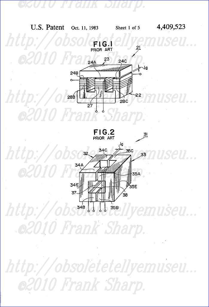
A prior-art saturable reactor apparatus for correcting pincushion distortion in a television receiver has a construction as shown in FIG. 1.
 In the pincushion distortion correction transformer 21 shown in FIG. 1, saturable E and I type cores 22 and 23 are held in face to face relationship to each other with a predetermined gap l g provided between them, a control coil 27 is wound on a central leg 24 A of the E type core 22, and first and second controlled coils 28 B and 28 C are wound on the respective opposite end legs 24 B and 24 C of the same core such that they operate differentially with respect to each other. For correcting horizontal pincushion distortions, a parabolic current changing at the vertical scanning frequency is caused through the control coil 27 to modulate the horizontal deflecting current flowing through the controlled coils 28 B and 28 C , thus obtaining a correction such that the horizontal deflection current becomes maximum at the center of the vertical scanning portion. The inductance L H of the transformer 21 is given as ##EQU1## where N H1 and N H2 are respectively turns numbers of the first and second controlled coils 28 B and 28 C (N H1 =N H2 ), l is the average length of the magnetic path, S is the sectional area of the core, and μ e is the effective magnetic permeability while μO is the magnetic permeability of a vacuum.
FIG. 2 shows a pincushion distortion correction transformer disclosed in a earlier patent application filed by the same applicant, and it is mentioned here for the purpose of faccilitating the understanding of the present invention. In this transformer 31, a control coil 37 and a controlled coil 38 are wound in a perpendicular relation to each other on legs 34 and 35 of a pair of four leg cores 32 and 33. The core 32 has a square or rectangular plate-like base portion 34 E and four legs 34 A to 34 D extending from the four corners of the base portion. The four legs have equal sectional area. Likewise, the core 33 has a base portion 35 E and four legs 35 A to 35 D . In FIG. 2, the legs 34 D and 35 D are concealed and not shown. The cores 32 and 33 having this construction are held such that the ends of the legs 34 A to 34 D of the former are respectively brought into contact with the corresponding legs 35 A to 35 D of the latter through predetermined gaps to define a constant space l g . The control coil 37 is wound on the legs 34 B and 34 D of the core 32 as a set, and the controlled coil 38 is wound on the legs 35 A and 35 B of the core 33 as a set. The inductance of this perpendicular transformer 31 is given as ##EQU2## N H in equation (2) is the turns number of the controlled coil 38 having almost half the turns of FIG. 1, and this means that for the example in FIG. 2 substantially the same variable inductance characteristic can be obtained with one half the turns number compared with the prior-art example of FIG. 1.
However, these pincushion distortion correction saturable reactor apparatus shown in FIGS. 1 and 2, have disadvantages; for example, raster shrinkage occurs in the neighborhood of the center of the screen, and the horizontal linearity is inferior.
 FIG. 3 is a graph showing the variable inductance characteristic of the perpendicular transformer 31 shown in FIG. 2. In this graph, the abscissa represents the horizontal deflecting current I H (in A), and the ordinate represents the inductance L H (in μH). The vertical deflecting current I V (in mA) is taken as the parameter, and characteristic curves for 0,10,20,40 mA respectively are shown. When the inductance characteristic is as shown in FIG. 3, the reproduction on the screen has a character as shown in FIG. 4. The reproduction shown in FIG. 4 is obtained when a reference pattern consisting of a plurality of uniformly spaced vertical lines is reproduced on the television screen after the horizontal pincushion distortion correction using the transformer 31 mentioned above. The ratio of the interline space in the reproduction of FIG. 4 with respect to the interline average space in the reference pattern (in %) is as shown in FIG. 5. It will be seen that the raster shrinkage is produced in the neighborhood of the center of the screen, particularly in a horizontal deflecting current region between from -1 to +1 A. Due to this shrinkage, the horizontal linearity is inferior. Therefore the dynamic range of the variable inductance defined by the DC superimposition characteristics thereof becomes narrow.
SUMMARY OF THE INVENTION
The present invention seeks to overcome the aforementioned drawback inherent in the prior art, and its object is to provide a pincushion distortion correction saturable reactor apparatus, which is simple in construction and can improve the variable inductance characteristic and preclude the distortion of deflection in the neighborhood of the center of the reproduction, thus permitting wide improvement of the horizontal linearity and extension of the DC superimposition variable inductance dynamic range.
In accordance with an aspect of present invention, the apparatus for correcting pincushion distortion comprises a core having a gap, a control coil and a controlled coil, the control and controlled coils being wound on the core in a perpendicular relation to each other, the gap having an unbalanced configuration in the path of magnetic flux produced by the controlled coil, the control coil supplying a parabolic current for pincushion distortion correction, and the controlled coil supplying a deflecting current to be corrected.
The above and other objects, features and advantages of the illustrated embodiments of the invention will appear from the description given below, which is to be read in connection with the accompanying drawings.
BRIEF DESCRIPTION OF THE DRAWINGS
FIG. 1 is a perspective view showing a prior art example.
FIGS. 2 through 5 illustrate information concerning a transformer, given for the purpose of facilitating the understanding of the present invention, and of which FIG. 2 is a perspective view of the transformer;
FIG. 3 is a graph showing the variable inductance characteristic in FIG. 1 or 2;
FIG. 4 is a plan view showing the reproduction on a television screen in example FIG. 1 or 2;
FIG. 5 is a graph showing the horizontal linearity;
FIGS. 6 and 7 show a first embodiment of the present invention, and of which FIG. 6 is a perspective view showing the apparatus before the assembly, and FIG. 7 is a perspective view showing the apparatus after the assembly.
FIGS. 8 through 13 show a second embodiment of the present invention, and of which FIG. 8 is a perspective view showing the apparatus before the assembly thereof, FIG. 9 is a perspective view showing the apparatus after assembly, FIG. 10 is a fragmentary perspective view of the apparatus for illustrating the operation thereof, FIG. 11 is a graph showing the variable inductance characteristic, FIG. 12 is a plan view showing the reproduction on a television screen, and FIG. 13 is a graph showing the horizontal linearity.
DETAILED DESCRIPTION OF THE PREFERRED EMBODIMENTS
Now, a preferred embodiment of the present invention will be described in conjunction with some preferred embodiments thereof with reference to the accompanying drawings.
 FIGS. 6 and 7 show a first embodiment of the pincushion distortion correction saturable reactor apparatus 1 according to the present invention. FIG. 6 shows a perspective view of the apparatus before the assembly thereof, and FIG. 7 shows a perspective view of the apparatus after assembly. In these Figures, the apparatus comprises cores 2 and 3 having an identical shape and made of a ferrite material. The core 2 has a plate-like base portion 4 E , for instance having a square or rectangular shape, and four legs 4 A ,4 B ,4 C and 4 D perpendicularly projecting from the four corners of one side of the base portion and having an equal sectional area. Likewise, the other core 3 has a base portion 5 E and four leg portions 5 A ,5 B ,5 C and 5 D . These cores 2 and 3 are arranged such that the legs 4 A to 4 D of the former abut on the corresponding legs 5 A to 5 D of the latter. More particularly, an adjacent two of the four legs of the core 2, for instance legs 4 A and 4 B are coupled to the corresponding legs of the other core, for instance legs 5 A and 5 B via a spacer 6. Thus, the faces of the legs facing each other are inclined with respect to each other, and the gap is increased toward the reader. The thickness of the spacer 6 is set substantially to 2 l g , i.e., double the gap interval l g in the afore-mentioned prior-art construction. A control coil 7 is wound on a pair of legs, namely the leg 4 B of the core 2 in contact with the spacer 6 and the leg 4 D adjacent to the leg 4 B but not in contact with the spacer 6. A controlled coil 8 is wound on a pair of legs 5 A and 5 B of the other core 3 in contact with the spacer 6. Alternatively, the controlled coil 8 may be wound on pair legs 5 C and 5 D which are not in contact with the spacer 6. The magnetic flux produced by the current through the control coil 7 passes through a loop constituted by the legs 4 A and 5 A and legs 5 B and 4 B. The magnetic flux produced by the current through the controlled coil 8 passes through a loop constituted by the legs 4 A and 5 A and legs 5 C and 4 C . Since the facing faces of the individual pairs of legs constituting the path of magnetic flux set up by the controlled coil 8 are inclined due to the spacer 6 interposed between the legs 4 A and 5 A and also between the legs 4 B and 5 B , the gap between these facing surfaces is increased toward the reader in the FIG. 7, that is, the gap formed in the path of magnetic flux set up by the controlled coil 8 has an unbalanced form. In the afore-mentioned prior-art example (shown in FIG. 2), in which the facing surfaces of the individual pair legs are parallel, the gaps in the magnetic flux paths for both the control and controlled coils are balanced in form.
 FIGS. 8 through 10 show a second embodiment of the present invention. In this embodiment of the pincushion distortion correction saturable reactor apparatus 11, a pair of cores 12 and 13 which have different shapes are used. The assembled form of the pincushion distortion saturable reactor apparatus 11 is practially the same as the apparatus of the first embodiment, but this embodiment is different from the first embodiment in the position, in which the core halves of the apparatus are coupled to each other, and the assembly can be more readily made.
More particularly, referring to FIGS. 8 and 10, the core 12 has a base portion 14 E , for instance having a square or rectangular shape, and four legs 14 A ,14 B ,14 C and 14 D perpendicularly projecting from the four corners of the base portion and somewhat a greater length (capable of accommodating two coils). The core 13, on the other hand, consists of a square or rectangular plate corresponding to the base portion of cores in the first embodiment.
These cores 12 and 13 are arranged such that they abut on each other with a spacer 6 provided in contact with two adjacent legs 14 A and 14 B of the core 12 to form a gap of an unbalanced form for the controlled coil 8. The coil 7 is wound on the set of legs 14 B and 14 D , and the controlled coil 8 is wound on a set of legs 14 A and 14 B in contact with the spacer 6. In this construction, the gap in the magnetic flux path for the controlled coil 8 varies for different portions of the facing surfaces and thus has an unbalanced form.
In the use of the first and second embodiments for the lateral pincushion distortion correction, parabolic current I V containing an appropriate DC bias is supplied to the control coil 7, and horizontal deflecting current I H is supplied to the controlled coil 8. In this case, the turns number N V of the control coil 7 is selected relatively large to reduce the exciting current I V so that a flux φ V within a saturating region is produced by the magnetizing force N V I V . For the control coil 8 a large diameter wire is used, and its turns number N H is set to a value necessary for obtaining the required variable inductance for the lateral pincushion distortion correction.
The first and second embodiments having the above constructions according to the present invention operate practically in the same way, so the operation of the second embodiment only will be described.
The flux φ V produced by the current I V through the control coil 7 passes through the leg 14 B , base portion 14 E and leg 14 A of the core 12 and the core 13 as shown by dashed arrows in FIG. 9. Also, although not shown, a flux is caused to pass through the leg 14 D , base portion 14 E and 14 C of the core 12 and core 13. On the other hand, the flux φ H produced by the current I H through the controlled coil 8 passes through a loop constituted by the leg 14 A , base portion 14 E and leg 14 C of the core 12 and the core 13 as shown by solid arrows in FIG. 9. These fluxes φ V and φ H do not link with each other, so that no induction voltage is produced. Thus, by causing a parabolic current at the vertical scanning frequency to flow through the control coil 7, the inductance of the controlled coil 8 can be varied to obtain the correction of the lateral pincushion distortion.
Now, the effects of the gap having the unbalanced form will be described. In a state when the magnetomotive force N V I V provided by the control coil 7 is less than the magnetomotive force N H I H provided by the controlled coil 8 (i.e., N V I V H I H ), the flux through the four legs 14 A to 14 D , and hence the magnetic permeability, is controlled by the magnetomotive force N H I H . Thus, in the neighborhood of the end faces of the legs 14 C and 14 D free from the spacer 6, the magnetic saturation in the core sets gradually in from the contact points of the legs 14 C and 14 D with the core 13, and substantially the similar variable inductance characteristic as that obtained with the balanced gap perpendicular transformer 31 shown in FIG. 2 can be obtained.
On the other hand, in a state when the magnetomotive force N V I V is greater than the magnetomotive force N H I H (i.e., N V I H >N H I H ), the saturation of the core in the neighborhood of the gaps defined by the end faces of the legs 14 C and 14 D is determined by the magnetomotive force N V I V . For the flux φ V , most flux flows in one loop through the legs 14 C and 14 D , because the other magnetic loop which includes the legs 14 A and 14 B has two wide gaps, therefore the magnetic reluctance of this loop is larger than that of the former. Therefore the large flux φ V concentrates at the contact points of the legs 14 C and 14 D . The concentration of flux makes the points saturate and, the saturated points act as the effective gaps. With the saturation in the neighborhood of the gaps defined by the legs 14 C and 14 D , the magnetic reluctance of the gaps is apparently increased. Also, the distance of the gap in the magnetic flux path for the controlled coil 8 is increased in the gaps defined by the legs 14 C and 14 D . The flux φ H and the apparent gap Δl g are shown in FIG. 10.
 With the apparent increase of the magnetic reluctance (i.e., increase of the gap distance), the inductance is reduced to L H , which is expressed as ##EQU3## where l is the average length of magnetic path, S is the sectional area of the core, and μ e is the effective permeability, while μ O is the permeability of a vacuum.
FIG. 11 shows the variable inductance characteristics of the pincushion distortion correction saturable reactor apparatus having the above construction. In the graph of FIG. 11, the ordinate is taken as the variable inductance L H ' in μH, and the abscissa is taken as the horizontal deflecting current I H in A. Characteristic curves shown are obtained when the vertical parabolic current I V is respectively 0,10,20 and 40 mA. These characteristic curves have substantially M-shaped forms with the variable inductance L H , reduced in an I H range in the neighborhood of 0 corresponding to the central portion of the screen. Thus, in the reproduction, the deflectional distortion in the central portion of the television screen can be widely improved as shown in FIG. 12. FIG. 12 is similar to FIG. 4, showing the reproduction of a reference pattern consisting of uniformly spaced vertical lines. In this case, extremely improved horizontal linearity compared with that shown in FIG. 5 can be obtained as shown in FIG. 13. Also, the dynamic range for the control coil current I V and controlled coil current I H can be increased. Further, with the same outer case size and current I H , a larger CRT size correction is possible even with a reduced value of current I V . Furthermore, with the same amplitude of control current, a larger CRT where the horizontal deflecting current is higher is possible to correct.
The characteristics of the prior-art reactor apparatus of FIG. 1, as shown in FIGS. 3 through 5, and the characteristics of the reactor apparatus according to the present invention, as shown in FIGS. 11 through 13, are based upon data obtained from experiments using a 20-inch color television receiver with a deflection angle of 100 degrees for 10% pincushion distortion correction. The relevant conditions and performance are shown in table 1.
A signal source means S is indicated in FIG. 7 for supplying a control parabolic signal to the control winding 7, and a deflection coil means D is indicated in FIG. 7 as being connected in series with the controlled winding 8, for the sake of diagrammatic illustration.
The data listed in Table 1 for the present invention are for the second embodiment. According to the present invention, the volume of the apparatus can be reduced to 0.58 times that of the prior-art apparatus. Also, the total weight can be reduced to 0.66 times that in the case of the prior art. Further, in the performance, the horizontal linearity can be improved, and the heat dissipation of the core can be reduced.
As has been described in the foregoing, with the pincushion distortion correction saturable reactor apparatus according to the present invention, which is a saturable transformer comprising a core having four legs and respective common portions (such as 4E, 5E, FIG. 7, and 13, 14E, FIG. 9), and controlled and control coils coupled to the core legs in a perpendicular relation to each other, the core gap for the controlled coil is provided in an unbalanced form, and a parabolic current at the vertical scanning frequency (or at horizontal scanning frequency) containing a superimposed DC component is caused, through the control coil, thus modulating the inductance of the controlled coil.
By the unbalance of the gap is meant that the gap distance varies with different portions of the facing surfaces defining the gap. This can be obtained by interposing a spacer between two of the four legs on which the controlled coil is wound as mentioned above or between the other two legs so that the surfaces forming the gap are inclined with respect to each other.
With this construction, the variable inductance is reduced in a region in which the magnetomotive force produced by the control coil is greater than that produced by the controlled coil and, as a whole, characteristic curves having M-shaped forms can be obtained. Thus, the deflectional distortion in the neighborhood of the center of the reproduction on the screen is reduced, so that horizontal linearity can be widely improved. In addition, the dynamic range of the variable inductance inclusive of the superimposed DC portion is extended, so that it is possible to obtain size reduction and wide cost reduction compared with the prior art. Further, it is possible to realize the reduction of heat dissipation of the core, reduction of the controlled power, reduction of the number of component parts connected to the transformer and also reduction of the area of the printed circuit board occupied by the transformer.
The above embodiments of the present invention are by no means limitative, and the invention may be applied to the top and bottom pincushion distortion correction as well. Also, various other changes and modifications are possible without departing from the scope and spirit of the present invention.
SONY DST EHT FBT TRANSFORMER Bobbin structure for high voltage transformers EHT Output.
A coil bobbin for a fly-back transformer or the like having a bobbin proper. A plurality of partition members or flanges are formed on the bobbin proper with a slot between adjacent ones. At least first and second coil units are formed in the bobbin proper, each having several slots, formed between the flanges, and first and second high voltage coils are wound on the first and second coil units in opposite directions, respectively. A rectifying means is connected in series to the first and second coil units, and a cut-off portion or recess is provided on each of the partition members. In this case, a wire lead of the coil units passes from one slot to an adjacent slot through the cut-off portion which is formed as a delta groove, and one side of the delta groove is corresponded to the tangent direction to the winding direction.
1. A fly-back transformer comprising a coil bobbin comprising a plurality of parallel spaced discs with a first adjacent plurality of said disc for med with delta shaped slots having first edges which extend tangentially to a first winding direction and a first winding wound on said first adjacent plurality of said discs in said first winding direction, a second adjacent plurality of said discs formed with delta shaped slots having first edges which extend tangentially to a second winding direction opposite said first winding direction and a second winding wound on said second adjacent plurality of said discs in said second winding direction, a third adjacent plurality of said discs formed with delta shaped slots having first edges which extend tangentially to said first winding direction and a third winding wound on said third adjacent plurality of said discs in said first winding direction and said second plurality of adjacent discs mounted between said first and third plurality of adjacent discs. 2. A fly-back transformer according to claim 1 wherein adjacent ones of said first adjacent plurality of discs are mounted such that their delta shaped slots are orientated 180 degrees relative to each other. 3. A fly-back transformer according to claim 2 including a first winding turning partition mounted between said first and second adjacent plurality of discs and formed with grooves and notches for changing winding direction between said first and second windings and a second winding turning partition mounted between said second and third adjacent plurality of discs and formed with grooves and notches for changing the winding direction between said second and third windings. 4. A fly-back transformer according to claim 3 wherein said first and second winding turning partitions are formed with winding guiding slots for guiding the winding between the first, second and third adjacent plurality of discs. 5. A fly-back transformer according to claim 2 including a first rectifying means connected between one end of said first winding and one end of said second winding, and a second rectifying means connected between the second end of said second winding and one end of said third winding. 6. A fly-back transformer according to claim 5 wherein the second end of said first winding is grounded and a third rectifying means connected between the second end of said third winding and an output terminal.
1. Field of the Invention
This invention relates to pincushion distortion correction apparatus and, more particularly, to an apparatus to this end having a control coil and a controlled coil, these coils being coupled to a saturable magnetic core in a perpendicular relation to each other.
2. Description of the Prior Art
A prior-art saturable reactor apparatus for correcting pincushion distortion in a television receiver has a construction as shown in FIG. 1.
In the pincushion distortion correction transformer 21 shown in FIG. 1, saturable E and I type cores 22 and 23 are held in face to face relationship to each other with a predetermined gap l g provided between them, a control coil 27 is wound on a central leg 24 A of the E type core 22, and first and second controlled coils 28 B and 28 C are wound on the respective opposite end legs 24 B and 24 C of the same core such that they operate differentially with respect to each other. For correcting horizontal pincushion distortions, a parabolic current changing at the vertical scanning frequency is caused through the control coil 27 to modulate the horizontal deflecting current flowing through the controlled coils 28 B and 28 C , thus obtaining a correction such that the horizontal deflection current becomes maximum at the center of the vertical scanning portion. The inductance L H of the transformer 21 is given as ##EQU1## where N H1 and N H2 are respectively turns numbers of the first and second controlled coils 28 B and 28 C (N H1 =N H2 ), l is the average length of the magnetic path, S is the sectional area of the core, and μ e is the effective magnetic permeability while μO is the magnetic permeability of a vacuum. FIG. 2 shows a pincushion distortion correction transformer disclosed in a earlier patent application filed by the same applicant, and it is mentioned here for the purpose of faccilitating the understanding of the present invention. In this transformer 31, a control coil 37 and a controlled coil 38 are wound in a perpendicular relation to each other on legs 34 and 35 of a pair of four leg cores 32 and 33. The core 32 has a square or rectangular plate-like base portion 34 E and four legs 34 A to 34 D extending from the four corners of the base portion. The four legs have equal sectional area. Likewise, the core 33 has a base portion 35 E and four legs 35 A to 35 D . In FIG. 2, the legs 34 D and 35 D are concealed and not shown. The cores 32 and 33 having this construction are held such that the ends of the legs 34 A to 34 D of the former are respectively brought into contact with the corresponding legs 35 A to 35 D of the latter through predetermined gaps to define a constant space l g . The control coil 37 is wound on the legs 34 B and 34 D of the core 32 as a set, and the controlled coil 38 is wound on the legs 35 A and 35 B of the core 33 as a set. The inductance of this perpendicular transformer 31 is given as ##EQU2## N H in equation (2) is the turns number of the controlled coil 38 having almost half the turns of FIG. 1, and this means that for the example in FIG. 2 substantially the same variable inductance characteristic can be obtained with one half the turns number compared with the prior-art example of FIG. 1.
However, these pincushion distortion correction saturable reactor apparatus shown in FIGS. 1 and 2, have disadvantages; for example, raster shrinkage occurs in the neighborhood of the center of the screen, and the horizontal linearity is inferior.
 FIG. 3 is a graph showing the variable inductance characteristic of the perpendicular transformer 31 shown in FIG. 2. In this graph, the abscissa represents the horizontal deflecting current I H (in A), and the ordinate represents the inductance L H (in μH). The vertical deflecting current I V (in mA) is taken as the parameter, and characteristic curves for 0,10,20,40 mA respectively are shown. When the inductance characteristic is as shown in FIG. 3, the reproduction on the screen has a character as shown in FIG. 4. The reproduction shown in FIG. 4 is obtained when a reference pattern consisting of a plurality of uniformly spaced vertical lines is reproduced on the television screen after the horizontal pincushion distortion correction using the transformer 31 mentioned above. The ratio of the interline space in the reproduction of FIG. 4 with respect to the interline average space in the reference pattern (in %) is as shown in FIG. 5. It will be seen that the raster shrinkage is produced in the neighborhood of the center of the screen, particularly in a horizontal deflecting current region between from -1 to +1 A. Due to this shrinkage, the horizontal linearity is inferior. Therefore the dynamic range of the variable inductance defined by the DC superimposition characteristics thereof becomes narrow.
 SUMMARY OF THE INVENTION
The present invention seeks to overcome the aforementioned drawback inherent in the prior art, and its object is to provide a pincushion distortion correction saturable reactor apparatus, which is simple in construction and can improve the variable inductance characteristic and preclude the distortion of deflection in the neighborhood of the center of the reproduction, thus permitting wide improvement of the horizontal linearity and extension of the DC superimposition variable inductance dynamic range.
In accordance with an aspect of present invention, the apparatus for correcting pincushion distortion comprises a core having a gap, a control coil and a controlled coil, the control and controlled coils being wound on the core in a perpendicular relation to each other, the gap having an unbalanced configuration in the path of magnetic flux produced by the controlled coil, the control coil supplying a parabolic current for pincushion distortion correction, and the controlled coil supplying a deflecting current to be corrected.
The above and other objects, features and advantages of the illustrated embodiments of the invention will appear from the description given below, which is to be read in connection with the accompanying drawings.
BRIEF DESCRIPTION OF THE DRAWINGS
FIG. 1 is a perspective view showing a prior art example.
FIGS. 2 through 5 illustrate information concerning a transformer, given for the purpose of facilitating the understanding of the present invention, and of which FIG. 2 is a perspective view of the transformer;
FIG. 3 is a graph showing the variable inductance characteristic in FIG. 1 or 2;
FIG. 4 is a plan view showing the reproduction on a television screen in example FIG. 1 or 2;
FIG. 5 is a graph showing the horizontal linearity;
FIGS. 6 and 7 show a first embodiment of the present invention, and of which FIG. 6 is a perspective view showing the apparatus before the assembly, and FIG. 7 is a perspective view showing the apparatus after the assembly.
FIGS. 8 through 13 show a second embodiment of the present invention, and of which FIG. 8 is a perspective view showing the apparatus before the assembly thereof, FIG. 9 is a perspective view showing the apparatus after assembly, FIG. 10 is a fragmentary perspective view of the apparatus for illustrating the operation thereof, FIG. 11 is a graph showing the variable inductance characteristic, FIG. 12 is a plan view showing the reproduction on a television screen, and FIG. 13 is a graph showing the horizontal linearity.
DETAILED DESCRIPTION OF THE PREFERRED EMBODIMENTS
Now, a preferred embodiment of the present invention will be described in conjunction with some preferred embodiments thereof with reference to the accompanying drawings.
 FIGS. 6 and 7 show a first embodiment of the pincushion distortion correction saturable reactor apparatus 1 according to the present invention. FIG. 6 shows a perspective view of the apparatus before the assembly thereof, and FIG. 7 shows a perspective view of the apparatus after assembly. In these Figures, the apparatus comprises cores 2 and 3 having an identical shape and made of a ferrite material. The core 2 has a plate-like base portion 4 E , for instance having a square or rectangular shape, and four legs 4 A ,4 B ,4 C and 4 D perpendicularly projecting from the four corners of one side of the base portion and having an equal sectional area. Likewise, the other core 3 has a base portion 5 E and four leg portions 5 A ,5 B ,5 C and 5 D . These cores 2 and 3 are arranged such that the legs 4 A to 4 D of the former abut on the corresponding legs 5 A to 5 D of the latter. More particularly, an adjacent two of the four legs of the core 2, for instance legs 4 A and 4 B are coupled to the corresponding legs of the other core, for instance legs 5 A and 5 B via a spacer 6. Thus, the faces of the legs facing each other are inclined with respect to each other, and the gap is increased toward the reader. The thickness of the spacer 6 is set substantially to 2 l g , i.e., double the gap interval l g in the afore-mentioned prior-art construction. A control coil 7 is wound on a pair of legs, namely the leg 4 B of the core 2 in contact with the spacer 6 and the leg 4 D adjacent to the leg 4 B but not in contact with the spacer 6. A controlled coil 8 is wound on a pair of legs 5 A and 5 B of the other core 3 in contact with the spacer 6. Alternatively, the controlled coil 8 may be wound on pair legs 5 C and 5 D which are not in contact with the spacer 6. The magnetic flux produced by the current through the control coil 7 passes through a loop constituted by the legs 4 A and 5 A and legs 5 B and 4 B. The magnetic flux produced by the current through the controlled coil 8 passes through a loop constituted by the legs 4 A and 5 A and legs 5 C and 4 C . Since the facing faces of the individual pairs of legs constituting the path of magnetic flux set up by the controlled coil 8 are inclined due to the spacer 6 interposed between the legs 4 A and 5 A and also between the legs 4 B and 5 B , the gap between these facing surfaces is increased toward the reader in the FIG. 7, that is, the gap formed in the path of magnetic flux set up by the controlled coil 8 has an unbalanced form. In the afore-mentioned prior-art example (shown in FIG. 2), in which the facing surfaces of the individual pair legs are parallel, the gaps in the magnetic flux paths for both the control and controlled coils are balanced in form.
  FIGS. 8 through 10 show a second embodiment of the present invention. In this embodiment of the pincushion distortion correction saturable reactor apparatus 11, a pair of cores 12 and 13 which have different shapes are used. The assembled form of the pincushion distortion saturable reactor apparatus 11 is practially the same as the apparatus of the first embodiment, but this embodiment is different from the first embodiment in the position, in which the core halves of the apparatus are coupled to each other, and the assembly can be more readily made.
 More particularly, referring to FIGS. 8 and 10, the core 12 has a base portion 14 E , for instance having a square or rectangular shape, and four legs 14 A ,14 B ,14 C and 14 D perpendicularly projecting from the four corners of the base portion and somewhat a greater length (capable of accommodating two coils). The core 13, on the other hand, consists of a square or rectangular plate corresponding to the base portion of cores in the first embodiment.
These cores 12 and 13 are arranged such that they abut on each other with a spacer 6 provided in contact with two adjacent legs 14 A and 14 B of the core 12 to form a gap of an unbalanced form for the controlled coil 8. The coil 7 is wound on the set of legs 14 B and 14 D , and the controlled coil 8 is wound on a set of legs 14 A and 14 B in contact with the spacer 6. In this construction, the gap in the magnetic flux path for the controlled coil 8 varies for different portions of the facing surfaces and thus has an unbalanced form.
In the use of the first and second embodiments for the lateral pincushion distortion correction, parabolic current I V containing an appropriate DC bias is supplied to the control coil 7, and horizontal deflecting current I H is supplied to the controlled coil 8. In this case, the turns number N V of the control coil 7 is selected relatively large to reduce the exciting current I V so that a flux φ V within a saturating region is produced by the magnetizing force N V I V . For the control coil 8 a large diameter wire is used, and its turns number N H is set to a value necessary for obtaining the required variable inductance for the lateral pincushion distortion correction.
The first and second embodiments having the above constructions according to the present invention operate practically in the same way, so the operation of the second embodiment only will be described.
The flux φ V produced by the current I V through the control coil 7 passes through the leg 14 B , base portion 14 E and leg 14 A of the core 12 and the core 13 as shown by dashed arrows in FIG. 9. Also, although not shown, a flux is caused to pass through the leg 14 D , base portion 14 E and 14 C of the core 12 and core 13. On the other hand, the flux φ H produced by the current I H through the controlled coil 8 passes through a loop constituted by the leg 14 A , base portion 14 E and leg 14 C of the core 12 and the core 13 as shown by solid arrows in FIG. 9. These fluxes φ V and φ H do not link with each other, so that no induction voltage is produced. Thus, by causing
a parabolic current at the vertical scanning frequency to flow through the control coil 7, the inductance of the controlled coil 8 can be varied to obtain the correction of the lateral pincushion distortion. Now, the effects of the gap having the unbalanced form will be described. In a state when the magnetomotive force N V I V provided by the control coil 7 is less than the magnetomotive force N H I H provided by the controlled coil 8 (i.e., N V I V H I H ), the flux through the four legs 14 A to 14 D , and hence the magnetic permeability, is controlled by the magnetomotive force N H I H . Thus, in the neighborhood of the end faces of the legs 14 C and 14 D free from the spacer 6, the magnetic saturation in the core sets gradually in from the contact points of the legs 14 C and 14 D with the core 13, and substantially the similar variable inductance characteristic as that obtained with the balanced gap perpendicular transformer 31 shown in FIG. 2 can be obtained.
On the other hand, in a state when the magnetomotive force N V I V is greater than the magnetomotive force N H I H (i.e., N V I H >N H I H ), the saturation of the core in the neighborhood of the gaps defined by the end faces of the legs 14 C and 14 D is determined by the magnetomotive force N V I V . For the flux φ V , most flux flows in one loop through the legs 14 C and 14 D , because the other magnetic loop which includes the legs 14 A and 14 B has two wide gaps, therefore the magnetic reluctance of this loop is larger than that of the former. Therefore the large flux φ V concentrates at the contact points of the legs 14 C and 14 D . The concentration of flux makes the points saturate and, the saturated points act as the effective gaps. With the saturation in the neighborhood of the gaps defined by the legs 14 C and 14 D , the magnetic reluctance of the gaps is apparently increased. Also, the distance of the gap in the magnetic flux path for the controlled coil 8 is increased in the gaps defined by the legs 14 C and 14 D . The flux φ H and the apparent gap Δl g are shown in FIG. 10.
 With the apparent increase of the magnetic reluctance (i.e., increase of the gap distance), the inductance is reduced to L H , which is expressed as ##EQU3## where l is the average length of magnetic path, S is the sectional area of the core, and μ e is the effective permeability, while μ O is the permeability of a vacuum.
 FIG. 11 shows the variable inductance characteristics of the pincushion distortion correction saturable reactor apparatus having the above construction. In the graph of FIG. 11, the ordinate is taken as the variable inductance L H ' in μH, and the abscissa is taken as the horizontal deflecting current I H in A. Characteristic curves shown are obtained when the vertical parabolic current I V is respectively 0,10,20 and 40 mA. These characteristic curves have substantially M-shaped forms with the variable inductance L H , reduced in an I H range in the neighborhood of 0 corresponding to the central portion of the screen. Thus, in the reproduction, the deflectional distortion in the central portion of the television screen can be widely improved as shown in FIG. 12. FIG. 12 is similar to FIG. 4, showing the reproduction of a reference pattern consisting of uniformly spaced vertical lines. In this case, extremely improved horizontal linearity compared with that shown in FIG. 5 can be obtained as shown in FIG. 13. Also, the dynamic range for the control coil current I V and controlled coil current I H can be increased. Further, with the same outer case size and current I H , a larger CRT size correction is possible even with a reduced value of current I V . Furthermore, with the same amplitude of control current, a larger CRT where the horizontal deflecting current is higher is possible to correct.
The characteristics of the prior-art reactor apparatus of FIG. 1, as shown in FIGS. 3 through 5, and the characteristics of the reactor apparatus according to the present invention, as shown in FIGS. 11 through 13, are based upon data obtained from experiments using a 20-inch color television receiver with a deflection angle of 100 degrees for 10% pincushion distortion correction. The relevant conditions and performance are shown in table 1.
A signal source means S is indicated in FIG. 7 for supplying a control parabolic signal to the control winding 7, and a deflection coil means D is indicated in FIG. 7 as being connected in series with the controlled winding 8, for the sake of diagrammatic illustration.
| TABLE 1 |
| ______________________________________ |
| Present Item Invention Prior Art |
| ______________________________________ |
Core Data Gap 75μ (unbalanced) 38 (balanced) N V /N H (turns ratio) 1200 T /16 T 900 T /9 T + 9 T Outer dimensions 18 × 18 × 22 mm 19 × 21.5 × 30 mm of core Volume of core 4608 mm 3 9747 mm 3 Total weight 38.5 g 58.5 g Performance Horizontal linearity +1.4%.about.-2.7% +6.3%.about.-5.7% Controlled power 0.6 W 0.8 W Heat generation 20° C. 30° C. from core |
| ______________________________________ |
As has been described in the foregoing, with the pincushion distortion correction saturable reactor apparatus according to the present invention, which is a saturable transformer comprising a core having four legs and respective common portions (such as 4E, 5E, FIG. 7, and 13, 14E, FIG. 9), and controlled and control coils coupled to the core legs in a perpendicular relation to each other, the core gap for the controlled coil is provided in an unbalanced form, and a parabolic current at the vertical scanning frequency (or at horizontal scanning frequency) containing a superimposed DC component is caused, through the control coil, thus modulating the inductance of the controlled coil.
By the unbalance of the gap is meant that the gap distance varies with different portions of the facing surfaces defining the gap. This can be obtained by interposing a spacer between two of the four legs on which the controlled coil is wound as mentioned above or between the other two legs so that the surfaces forming the gap are inclined with respect to each other.
With this construction, the variable inductance is reduced in a region in which the magnetomotive force produced by the control coil is greater than that produced by the controlled coil and, as a whole, characteristic curves having M-shaped forms can be obtained. Thus, the deflectional distortion in the neighborhood of the center of the reproduction on the screen is reduced, so that horizontal linearity can be widely improved. In addition, the dynamic range of the variable inductance inclusive of the superimposed DC portion is extended, so that it is possible to obtain size reduction and wide cost reduction compared with the prior art. Further, it is possible to realize the reduction of heat dissipation of the core, reduction of the controlled power, reduction of the number of component parts connected to the transformer and also reduction of the area of the printed circuit board occupied by the transformer.
The above embodiments of the present invention are by no means limitative, and the invention may be applied to the top and bottom pincushion distortion correction as well. Also, various other changes and modifications are possible without departing from the scope and spirit of the present invention.
SONY DST EHT FBT TRANSFORMER Bobbin structure for high voltage transformers EHT Output.
A coil bobbin for a fly-back transformer or the like having a bobbin proper. A plurality of partition members or flanges are formed on the bobbin proper with a slot between adjacent ones. At least first and second coil units are formed in the bobbin proper, each having several slots, formed between the flanges, and first and second high voltage coils are wound on the first and second coil units in opposite directions, respectively. A rectifying means is connected in series to the first and second coil units, and a cut-off portion or recess is provided on each of the partition members. In this case, a wire lead of the coil units passes from one slot to an adjacent slot through the cut-off portion which is formed as a delta groove, and one side of the delta groove is corresponded to the tangent direction to the winding direction.
1. A fly-back transformer comprising a coil bobbin comprising a plurality of parallel spaced discs with a first adjacent plurality of said disc for
med with delta shaped slots having first edges which extend tangentially to a first winding direction and a first winding wound on said first adjacent plurality of said discs in said first winding direction, a second adjacent plurality of said discs formed with delta shaped slots having first edges which extend tangentially to a second winding direction opposite said first winding direction and a second winding wound on said second adjacent plurality of said discs in said second winding direction, a third adjacent plurality of said discs formed with delta shaped slots having first edges which extend tangentially to said first winding direction and a third winding wound on said third adjacent plurality of said discs in said first winding direction and said second plurality of adjacent discs mounted between said first and third plurality of adjacent discs. 2. A fly-back transformer according to claim 1 wherein adjacent ones of said first adjacent plurality of discs are mounted such that their delta shaped slots are orientated 180 degrees relative to each other. 3. A fly-back transformer according to claim 2 including a first winding turning partition mounted between said first and second adjacent plurality of discs and formed with grooves and notches for changing winding direction between said first and second windings and a second winding turning partition mounted between said second and third adjacent plurality of discs and formed with grooves and notches for changing the winding direction between said second and third windings. 4. A fly-back transformer according to claim 3 wherein said first and second winding turning partitions are formed with winding guiding slots for guiding the winding between the first, second and third adjacent plurality of discs. 5. A fly-back transformer according to claim 2 including a first rectifying means connected between one end of said first winding and one end of said second winding, and a second rectifying means connected between the second end of said second winding and one end of said third winding. 6. A fly-back transformer according to claim 5 wherein the second end of said first winding is grounded and a third rectifying means connected between the second end of said third winding and an output terminal.
Description:
BACKGROUND OF THE INVENTION
1. Field of the Invention
The present invention relates generally to a bobbin structure for high voltage transformers, and is directed more particularly to a bobbin structure for high voltage transformer suitable for automatically winding coils thereon.
2. Description of the Prior Art
In the art, when a wire lead is reversely wound on a bobbin separately at every winding block, a boss is provided at every winding block and the wire lead is wound on one block, then one end of the wire lead is tied to the boss where it will be cut off. The end of the wire lead is tied to another boss, and then the wire lead is wound in the opposite direction. Therefore, the prior art winding method requires complicated procedures and the winding of the wire lead cannot be rapidly done and also the winding can not be performed automatically. Further, the goods made by the prior art method are rather unsatisfactory and have a low yield.
OBJECTS AND SUMMARY OF THE INVENTION
Accordingly an object of the invention is to provide a coil bobbin for a fly-back transformer or the like by which a wire lead can be automatically wound on winding blocks of the coil bobbin even though the winding direction is different among the different winding blocks.
Another object of the invention is to provide a coil bobbin for a fly-back transformer or the like in which a bridge member and an inverse engaging device for transferring a wire lead from one wiring block to an adjacent wiring block of the coil bobbin and wiring the wire lead in opposite wiring directions between adjacent wiring blocks, and a guide member for positively guiding the wire lead are provided.
According to an aspect of the present invention, a coil bobbin for a fly-back transformer or the like is provided which comprises a plurality of partition members forming a plurality of slots, a first coil unit having several slots on which a first high voltage coil is wound in one winding direction, a second coil unit having several slots on which a second high voltage coil is wound in the other direction, a rectifying means connected in series to the first and second coil units, and a cut-off portion provided on each of the partition members, a wire lead passing from one slot to an adjacent slot through the cut-off portions, each of the cut-off portions being formed as a delta groove, and one side of the delta groove corresponding to a tangent to the winding direction.
The other objects, features and advantages of the present invention will become apparent from the following description taken in conjunction with the accompanying drawings through which the like reference numerals and letters designate the same elements and parts, respectively.
BRIEF DESCRIPTION OF THE DRAWINGS
FIG. 1 is a schematic diagram showing the construction of a fly-back transformer;
FIG. 2 is a connection diagram showing an example of the electrical connection of the fly-back transformer shown in FIG. 1;
FIG. 3 is a schematic diagram showing an example of a device for automatically winding a wire lead of the fly-back transformer on its bobbin;
FIG. 4 is a perspective view showing an example of the coil bobbin according to the present invention;
FIG. 5 is a plan view of FIG. 4;
FIGS. 6 and 7 are views used for explaining recesses or cut-off portions shown in FIGS. 4 and 5; and FIGS. 8A and 8B cross-sectional views showing an example of the inverse engaging means according to the present invention.
DESCRIPTION OF THE PREFERRED EMBODIMENT
When the high voltage winding of a fly-back transformer used in a high voltage generating circuit of a television receiver is divided into plural ones and then wound on a bobbin, the divided windings (divided coils) are connected in serie s through a plurality of rectifying diodes.
When the winding is divided into, for example, three portions, such as divided coils La, Lb and Lc, they are wound on a bobbin proper 1 from, for example, left to right sequentially in this order as shown in FIG. 1. In this case, if the divided coils La and Lc are selected to have the same sense of turn and the middle coil Lb is selected to have the opposite sense of turn from the coils La and Lc, the distance between the terminal end of coil La and the start of coil Lb and the distance between the terminal end of coil Lb and the start of coil Lc can be got relatively long. Therefore, diodes Da and Db can be mounted by utilizing the space above the block on which the middle coil Lb is wound as shown in FIG. 1, so that it becomes useless to provide spaces for diodes between the divided coils La and Lb and between the divided coils Lb and Lc and hence the bobbin proper 1 can be made compact.
FIG. 2 is a connection diagram showing the connection of the above fly-back transformer. In FIG. 2, reference numeral 2 designates a primary winding (Primary coil) of the fly-back transformer, reference letter L designates its high voltage winding (secondary coil), including divided coils La, Lb and Lc, 3 an output terminal, and 4 a lead wire connected to the anode terminal of a cathode ray tube (not shown), respectively.
An example of the bobbin structure according to the invention, which is suitable to automatically wind coils, which are different in sense of turn in each winding block as shown in FIG. 1, on the bobbin, will be hereinafter described with reference to the drawings.
FIG. 3 is a diagram showing an automatic winding apparatus of a wire lead on a coil bobbin. If it is assumed that the wire lead is wound in the order of w inding blocks A, B and C in FIG. 1 and the wire lead is wound on the block A with the bobbin proper 1 being rotated in the counter-clockwise direction as shown in FIG. 3, the relation between the bobbin proper 1 and the wire lead becomes as shown in FIG. 3. In this figure, reference numeral 6 designates a bobbin for feeding the wire lead.
Turning to FIG. 4, an example 10 of the bobbin structure or coil bobbin according to the present invention will be described now. In this example, the winding blocks A, B and C for the divided coils La, Lb and Lc are respectively divided into plural slots or sections by plural partition members or flanges 11, and a cut-off portion or recess 12 is formed on each of the flanges 11 through which the wire lead in one section is transferred to the following winding section.
As shown in FIG. 6, each recess 12 is so formed that its one side extends in the direction substantially coincident with the tangent to the circle of the bobbin proper 1 and its direction is selected in response to the sense of turn of the winding or wire lead. In this case, the direction of recess 12 means the direction of the opening of recess 12, and the direction of recess 12 is selected opposite to the sense of turn of the wi nding in the present invention.
Now, recesses 12A, which are formed in the winding block A, will be now described by way of example. The positions of recesses 12A formed on an even flange 11Ae and an odd flange 11A 0 are different, for example, about 180° as shown in FIGS. 6A and 6B. Since the bobbin proper 1 is rotated in the counter-clockwise direction in the winding block A and hence the sense of turn of the wire lead is in the clockwise direction, the recess 12A is formed on the even flange 11Ae at the position shown in FIG. 6A. That is, the direction of recess 12A is inclined with respect to the rotating direction of bobbin proper 1 as shown in FIG. 6A. In this case, one side 13a of recess 12A is coincident with the tangent to the circle of bobbin proper 1, while the other side 13b of recess 12A is selected to have an oblique angle with respect to the side 13a so that the recess 12A has a predetermined opening angle.
The opening angle of recess 12A is important but the angle between the side 13a of recess 12A and the tangent to the circle of bobbin proper 1 is also important in the invention. When the wire lead is bridged or transferred from one section to the following section through the recess 12A, the wire lead in one section advances to the following section in contact with the side 13a of recess 12A since the bobbin proper 1 is rotated. In the invention, if the side 13a of recess 12A is selected to be extended in the direction coincident with the tangent to the circle of bobbin proper 1, the wire lead can smoothly advance from one section to the next section without being bent.
In the invention, since the middle divided coil Lb is wound opposite to the divided coil La, a recess 12B provided on each of flanges 11B of the winding block B is formed to have an opening opposite to that of recess 12A formed in the winding block A as shown in FIGS. 6C and 6D.
As shown in FIG. 5, terminal attaching recesses 14 are provided between the winding blocks A and B to which diodes are attached respectively. In the illustrated example of FIG. 5, a flange 15AB is formed between the flanges 11A 0 and 11B 0 of winding blocks A and B, and the recesses 14 are formed between the flanges 11A 0 and 15AB and between 15AB and 11B 0 at predetermined positions. Then, terminal plates 16, shown in FIG. 4, are inserted into the recesses 14 and then fixed there to, respectively. The terminal plates 16 are not shown in FIG. 5. Between the winding blocks B and C and between the blocks A and B, similar terminal attaching recesses 14 are formed, and terminal plates 16 are also inserted thereinto and then fixed thereto.
As described above, since the divided coil Lb is wound opposite to the divided coils La and Lc, it is necessary that the winding direction of the wire lead be changed when the wire lead goes from the block A to block B and also from the block B to block C, respectively.
Turning to FIG. 7, an example of the winding or wire lead guide means according to the present invention will be now described. In FIG. 7, there are mainly shown a bridge member for the wire lead and an inve rse member or means for the wire lead which are provided between the winding blocks A and B. At first, a bridge means 20 and its guide means 21, which form the bridge member, will be described. The bridge means 20 is provided by forming a cut-out portion or recess in the middle flange 15AB located between the winding blocks A and B. In close relation to the bridge means or recess 20, the guide means 21 is provided on a bridge section X A at the side of block A. This guide means 21 is formed as a guide piece which connects an edge portion 20a of recess 20 at the winding direction side to the flange 11A 0 of block A in the oblique direction along the winding direction through the section X A .
Next, an inverse engaging means 22 will be now described with reference to FIGS. 7 and 8. If the flange 11B 0 of FIG. 7 is viewed from the right side, the inverse engaging means 22 can be shown in FIG. 8A. In this case, the tip end of one side 13a of recess 12B 1 is formed as a projection which is extended outwards somewhat beyond the outer diameter of flange 11B 0 . The inverse engaging means 22 may take any configuration but it is necessary that when the rotating direction of the bobbin proper 1 is changed to the clockwise direction, the wire lead can be engaged with the recess 12B 1 or projection of one side 13a and then suitably transferred to the next station.
Another guide means 23 is provided on a bridge section X B at the side of winding block B in close relation to the inverse engaging means 22. The guide means 23 is formed as a guide surface which is a projected surface from the bottom surfa ce of section X B and extended obliquely in the winding direction. This guide means or guide surface 23 is inclinded low into the means 22 and has an edge 23a which is continuously formed between the middle flange 15AB and the flange 11B 0 .
In this case, it is possible that the guide means 21 and guide surface 23 are formed to be the same in construction. That is, both the guide means 21 and 23 can be made of either the guide piece, which crosses the winding section or guide surface projected upwards from the bottom surface of the winding section. It is sufficient if the guide means 21 and 23 are formed to smoothly transfer the wire lead from one section to the next section under the bobbin proper 1 being rotated.
Although not shown, in connection with the middle flange 15BC between the winding blocks B and C, there are provided similar bridge means 20, guide means 21, inverse engaging means 22 and another guide means 23, respectively. In this case, since the winding direction of the wire lead is reversed, the forming directions of the means are reverse but their construction is substantially the same as that of the former means. Therefore, their detailed description will be omitted.
According to the bobbin structure of the invention with the construction set forth above, the wire lead, which is transferred from the block A to the section X A by the rotation of bobbin proper 1, is wound on the section X B from the section X A after being guided by the guide piece 21 to the recess 20 provided on the middle flange 15AB, and then transferred to the recess 22 provided on the flange 11B 0 guide surface 23, bridged once to the first section of winding block B through the recess 22 (refer to dotted lines b in FIG. 7). Then, if the rotating direction of the bobbin proper 1 is reversed, the wire lead is engaged with the bottom of recess 22 (refer to solid lines b in FIG. 7). Thus, if the above reverse rotation of bobbin proper 1 is maintained, the wire lead is wound on the block B in the direction reverse to that of block A. When the wire lead is transferred from the block B to block C, the same effect as that above is achieved. Therefore, according to the present invention, the wire lead can be automatically and continuously wound on the bobbin proper 1.
After the single wire lead is continuously wound on blocks A, B and C of bobbin proper 1 as set forth above, the wire lead is cut at the substantially center of each of its bridging portions. Then, the cut ends of the wire lead are connected through diodes Da, Db and Dc at the terminal plates 16, respectively by solder.
In the present invention, the projection piece, which has the diameter greater than that of the flange 11B, is provided in the bridge recess 12 to form the inverse engaging means 22 as described above, so that when the winding direction is changed, the wire lead engages with the inverse engaging means 22 without errors when reversing the winding direction of the wire lead.
If the diameter of the projection piece of means 22 is selected, for example, to be the same as that of the flange 11B, it will not be certain that the wire lead engages with the means 22 because it depends upon the extra length of the wire lead and hence errors in winding cannot be positively avoided.
Further, in this invention, the bridge means is provided on the flange positioned at the bridging portion of the bobbin which has a number of dividing blocks separated by flanges, and the inverse engaging means is provided and also the guide means is provided at the former winding section to cooperate with the inverse engaging means. Therefore, the wire lead can be positively fed to the bridge means, and the transfer of the wire lead to the following winding section can be carried out smoothly.
Further, in this invention since one side of the recess 12 is selected coincident with the tangent of the outer circle of the bobbin proper 1 and also with the winding direction, the wire lead can be smoothly bridged to the following section. Due to the fact that the direction of recess 12 is changed in response to the winding direction, even if there is a block on which the wire lead is wound in the opposite direction to that of the other block, the wire lead can be continuously and automatically wound through the respective blocks.
The above description is given for the case where the present invention is applied to the coil bobbin for the high voltage winding of a fly-back transformer, but it will be clear that the present invention can be applied to other coil bobbins which require divided windings thereon with the same effects.
It will be apparent that many modifications and variations could be effected by one skilled in the art without departing from the spirits or scope of the novel concepts of the present invention, so that the spirits or scope of the invention should be determined by the appended claims only.
1. Field of the Invention
The present invention relates generally to a bobbin structure for high voltage transformers, and is directed more particularly to a bobbin structure for high voltage transformer suitable for automatically winding coils thereon.
2. Description of the Prior Art
In the art, when a wire lead is reversely wound on a bobbin separately at every winding block, a boss is provided at every winding block and the wire lead is wound on one block, then one end of the wire lead is tied to the boss where it will be cut off. The end of the wire lead is tied to another boss, and then the wire lead is wound in the opposite direction. Therefore, the prior art winding method requires complicated procedures and the winding of the wire lead cannot be rapidly done and also the winding can not be performed automatically. Further, the goods made by the prior art method are rather unsatisfactory and have a low yield.
OBJECTS AND SUMMARY OF THE INVENTION
Accordingly an object of the invention is to provide a coil bobbin for a fly-back transformer or the like by which a wire lead can be automatically wound on winding blocks of the coil bobbin even though the winding direction is different among the different winding blocks.
Another object of the invention is to provide a coil bobbin for a fly-back transformer or the like in which a bridge member and an inverse engaging device for transferring a wire lead from one wiring block to an adjacent wirin
g block of the coil bobbin and wiring the wire lead in opposite wiring directions between adjacent wiring blocks, and a guide member for positively guiding the wire lead are provided. According to an aspect of the present invention, a coil bobbin for a fly-back transformer or the like is provided which comprises a plurality of partition members forming a plurality of slots, a first coil unit having several slots on which a first high voltage coil is wound in one winding direction, a second coil unit having several slots on which a second high voltage coil is wound in the other direction, a rectifying means connected in series to the first and second coil units, and a cut-off portion provided on each of the partition members, a wire lead passing from one slot to an adjacent slot through the cut-off portions, each of the cut-off portions being formed as a delta groove, and one side of the delta groove corresponding to a tangent to the winding direction.
The other objects, features and advantages of the present invention will become apparent from the following description taken in conjunction with the accompanying drawings through which the like reference numerals and letters designate the same elements and parts, respectively.
BRIEF DESCRIPTION OF THE DRAWINGS
FIG. 1 is a schematic diagram showing the construction of a fly-back transformer;
FIG. 2 is a connection diagram showing an example of the electrical connection of the fly-back transformer shown in FIG. 1;
FIG. 3 is a schematic diagram showing an example of a device for automatically winding a wire lead of the fly-back transformer on its bobbin;
FIG. 4 is a perspective view showing an example of the coil bobbin according to the present invention;
FIG. 5 is a plan view of FIG. 4;
FIGS. 6 and 7 are views used for explaining recesses or cut-off portions shown in FIGS. 4 and 5; and FIGS. 8A and 8B cross-sectional views showing an example of the inverse engaging means according to the present invention.
DESCRIPTION OF THE PREFERRED EMBODIMENT
When the high voltage winding of a fly-back transformer used in a high voltage generating circuit of a television receiver is divided into plural ones and then wound on a bobbin, the divided windings (divided coils) are connected in serie
 s through a plurality of rectifying diodes.
 When the winding is divided into, for example, three portions, such as divided coils La, Lb and Lc, they are wound on a bobbin proper 1 from, for example, left to right sequentially in this order as shown in FIG. 1. In this case, if the divided coils La and Lc are selected to have the same sense of turn and the middle coil Lb is selected to have the opposite sense of turn from the coils La and Lc, the distance between the terminal end of coil La and the start of coil Lb and the distance between the terminal end of coil Lb and the start of coil Lc can be got relatively long. Therefore, diodes Da and Db can be mounted by utilizing the space above the block on which the middle coil Lb is wound as shown in FIG. 1, so that it becomes useless to provide spaces for diodes between the divided coils La and Lb and between the divided coils Lb and Lc and hence the bobbin proper 1 can be made compact.
FIG. 2 is a connection diagram showing the connection of the above fly-back transformer. In FIG. 2, reference numeral 2 designates a primary winding (Primary coil) of the fly-back transformer, reference letter L designates its high voltage winding (secondary coil), including divided coils La, Lb and Lc, 3 an output terminal, and 4 a lead wire connected to the anode terminal of a cathode ray tube (not shown), respectively.
An example of the bobbin structure according to the invention, which is suitable to automatically wind coils, which are different in sense of turn in each winding block as shown in FIG. 1, on the bobbin, will be hereinafter described with reference to the drawings.
FIG. 3 is a diagram showing an automatic winding apparatus of a wire lead on a coil bobbin. If it is assumed that the wire lead is wound in the order of w
 inding blocks A, B and C in FIG. 1 and the wire lead is wound on the block A with the bobbin proper 1 being rotated in the counter-clockwise direction as shown in FIG. 3, the relation between the bobbin proper 1 and the wire lead becomes as shown in FIG. 3. In this figure, reference numeral 6 designates a bobbin for feeding the wire lead.
 Turning to FIG. 4, an example 10 of the bobbin structure or coil bobbin according to the present invention will be described now. In this example, the winding blocks A, B and C for the divided coils La, Lb and Lc are respectively divided into plural slots or sections by plural partition members or flanges 11, and a cut-off portion or recess 12 is formed on each of the flanges 11 through which the wire lead in one section is transferred to the following winding section.
As shown in FIG. 6, each recess 12 is so formed that its one side extends in the direction substantially coincident with the tangent to the circle of the bobbin proper 1 and its direction is selected in response to the sense of turn of the winding or wire lead. In this case, the direction of recess 12 means the direction of the opening of recess 12, and the direction of recess 12 is selected opposite to the sense of turn of the wi
 nding in the present invention.
 Now, recesses 12A, which are formed in the winding block A, will be now described by way of example. The positions of recesses 12A formed on an even flange 11Ae and an odd flange 11A 0 are different, for example, about 180° as shown in FIGS. 6A and 6B. Since the bobbin proper 1 is rotated in the counter-clockwise direction in the winding block A and hence the sense of turn of the wire lead is in the clockwise direction, the recess 12A is formed on the even flange 11Ae at the position shown in FIG. 6A. That is, the direction of recess 12A is inclined with respect to the rotating direction of bobbin proper 1 as shown in FIG. 6A. In this case, one side 13a of recess 12A is coincident with the tangent to the circle of bobbin proper 1, while the other side 13b of recess 12A is selected to have an oblique angle with respect to the side 13a so that the recess 12A has a predetermined opening angle.
The opening angle of recess 12A is important but the angle between the side 13a of recess 12A and the tangent to the circle of bobbin proper 1 is also important in the invention. When the wire lead is bridged or transferred from one section to the following section through the recess 12A, the wire lead in one section advances to the following section in contact with the side 13a of recess 12A since the bobbin proper 1 is rotated. In the invention, if the side 13a of recess 12A is selected to be extended in the direction coincident with the tangent to the circle of bobbin proper 1, the wire lead can smoothly advance from one section to the next section without being bent.
In the invention, since the middle divided coil Lb is wound opposite to the divided coil La, a recess 12B provided on each of flanges 11B of the winding block B is formed to have an opening opposite to that of recess 12A formed in the winding block A as shown in FIGS. 6C and 6D.
As shown in FIG. 5, terminal attaching recesses 14 are provided between the winding blocks A and B to which diodes are attached respectively. In the illustrated example of FIG. 5, a flange 15AB is formed between the flanges 11A 0 and 11B 0 of winding blocks A and B, and the recesses 14 are formed between the flanges 11A 0 and 15AB and between 15AB and 11B 0 at predetermined positions. Then, terminal plates 16, shown in FIG. 4, are inserted into the recesses 14 and then fixed there to, respectively. The terminal plates 16 are not shown in FIG. 5. Between the winding blocks B and C and between the blocks A and B, similar terminal attaching recesses 14 are formed, and terminal plates 16 are also inserted thereinto and then fixed thereto.
As described above, since the divided coil Lb is wound opposite to the divided coils La and Lc, it is necessary that the winding direction of the wire lead be changed when the wire lead goes from the block A to block B and also from the block B to block C, respectively.
Turning to FIG. 7, an example of the winding or wire lead guide means according to the present invention will be now described. In FIG. 7, there are mainly shown a bridge member for the wire lead and an inve
 rse member or means for the wire lead which are provided between the winding blocks A and B. At first, a bridge means 20 and its guide means 21, which form the bridge member, will be described. The bridge means 20 is provided by forming a cut-out portion or recess in the middle flange 15AB located between the winding blocks A and B. In close relation to the bridge means or recess 20, the guide means 21 is provided on a bridge section X A at the side of block A. This guide means 21 is formed as a guide piece which connects an edge portion 20a of recess 20 at the winding direction side to the flange 11A 0 of block A in the oblique direction along the winding direction through the section X A .
 Next, an inverse engaging means 22 will be now described with reference to FIGS. 7 and 8. If the flange 11B 0 of FIG. 7 is viewed from the right side, the inverse engaging means 22 can be shown in FIG. 8A. In this case, the tip end of one side 13a of recess 12B 1 is formed as a projection which is extended outwards somewhat beyond the outer diameter of flange 11B 0 . The inverse engaging means 22 may take any configuration but it is necessary that when the rotating direction of the bobbin proper 1 is changed to the clockwise direction, the wire lead can be engaged with the recess 12B 1 or projection of one side 13a and then suitably transferred to the next station.
Another guide means 23 is provided on a bridge section X B at the side of winding block B in close relation to the inverse engaging means 22. The guide means 23 is formed as a guide surface which is a projected surface from the bottom surfa
ce of section X B and extended obliquely in the winding direction. This guide means or guide surface 23 is inclinded low into the means 22 and has an edge 23a which is continuously formed between the middle flange 15AB and the flange 11B 0 . In this case, it is possible that the guide means 21 and guide surface 23 are formed to be the same in construction. That is, both the guide means 21 and 23 can be made of either the guide piece, which crosses the winding section or guide surface projected upwards from the bottom surface of the winding section. It is sufficient if the guide means 21 and 23 are formed to smoothly transfer the wire lead from one section to the next section under the bobbin proper 1 being rotated.
Although not shown, in connection with the middle flange 15BC between the winding blocks B and C, there are provided similar bridge means 20, guide means 21, inverse engaging means 22 and another guide means 23, respectively. In this case, since the winding direction of the wire lead is reversed, the forming directions of the means are reverse but their construction is substantially the same as that of the former means. Therefore, their detailed description will be omitted.
According to the bobbin structure of the invention with the construction set forth above, the wire lead, which is transferred from the block A to the section X A by the rotation of bobbin proper 1, is wound on the section X B from the section X A after being guided by the guide piece 21 to the recess 20 provided on the middle flange 15AB, and then transferred to the recess 22 provided on the flange 11B 0 guide surface 23, bridged once to the first section of winding block B through the recess 22 (refer to dotted lines b in FIG. 7). Then, if the rotating direction of the bobbin proper 1 is reversed, the wire lead is engaged with the bottom of recess 22 (refer to solid lines b in FIG. 7). Thus, if the above reverse rotation of bobbin proper 1 is maintained, the wire lead is wound on the block B in the direction reverse to that of block A. When the wire lead is transferred from the block B to block C, the same effect as that above is achieved. Therefore, according to the present invention, the wire lead can be automatically and continuously wound on the bobbin proper 1.
After the single wire lead is continuously wound on blocks A, B and C of bobbin proper 1 as set forth above, the wire lead is cut at the substantially center of each of its bridging portions. Then, the cut ends of the wire lead are connected through diodes Da, Db and Dc at the terminal plates 16, respectively by solder.
In the present invention, the projection piece, which has the diameter greater than that of the flange 11B, is provided in the bridge recess 12 to form the inverse engaging means 22 as described above, so that when the winding direction is changed, the wire lead engages with the inverse engaging means 22 without errors when reversing the winding direction of the wire lead.
If the diameter of the projection piece of means 22 is selected, for example, to be the same as that of the flange 11B, it will not be certain that the wire lead engages with the means 22 because it depends upon the extra length of the wire lead and hence errors in winding cannot be positively avoided.
Further, in this invention, the bridge means is provided on the flange positioned at the bridging portion of the bobbin which has a number of dividing blocks separated by flanges, and the inverse engaging means is provided and also the guide means is provided at the former winding section to cooperate with the inverse engaging means. Therefore, the wire lead can be positively fed to the bridge means, and the transfer of the wire lead to the following winding section ca
n be carried out smoothly. Further, in this invention since one side of the recess 12 is selected coincident with the tangent of the outer circle of the bobbin proper 1 and also with the winding direction, the wire lead can be smoothly bridged to the following section. Due to the fact that the direction of recess 12 is changed in response to the winding direction, even if there is a block on which the wire lead is wound in the opposite direction to that of the other block, the wire lead can be continuously and automatically wound through the respective blocks.
The above description is given for the case where the present invention is applied to the coil bobbin for the high voltage winding of a fly-back transformer, but it will be clear that the present invention can be applied to other coil bobbins which require divided windings thereon with the same effects.
It will be apparent that many modifications and variations could be effected by one skilled in the art without departing from the spirits or scope of the novel concepts of the present invention, so that the spirits or scope of the invention should be determined by the appended claims only.
No comments:
Post a Comment
The most important thing to remember about the Comment Rules is this:
The determination of whether any comment is in compliance is at the sole discretion of this blog’s owner.
Comments on this blog may be blocked or deleted at any time.
Fair people are getting fair reply. Spam and useless crap and filthy comments / scrapers / observations goes all directly to My Private HELL without even appearing in public !!!
The fact that a comment is permitted in no way constitutes an endorsement of any view expressed, fact alleged, or link provided in that comment by the administrator of this site.
This means that there may be a delay between the submission and the eventual appearance of your comment.
Requiring blog comments to obey well-defined rules does not infringe on the free speech of commenters.
Resisting the tide of post-modernity may be difficult, but I will attempt it anyway.
Your choice.........Live or DIE.
That indeed is where your liberty lies.
Note: Only a member of this blog may post a comment.