


- A completely NEW design of power supply was developed By GRUNDIG when designing the CUC720 CUC740 CHASSIS SERIES.
Based on TDA4600 (SIEMENS) was Universally used for very long time since the design Of the CHASSIS CUC720 is the father of all chassis design from 1981 to the end of GRUNDIG productions, employing a varyiety of versions type of the control IC (TDA460X) except for CHASSIS CUC2201 and CUC3400 and CUC3410 and CUC3510 which they're based on other technology.
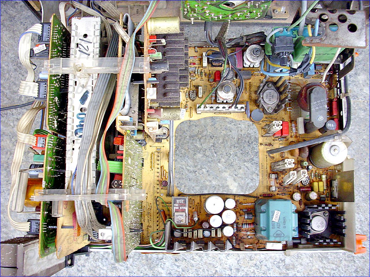
GRUNDIG SUPER COLOR B7502 SERIE 3022 SUPERSOUND CHASSIS CUC740 Power supply Description based on TDA4600 (SIEMENS)
 3 charges when the chopper is on and is discharged when the chopper is off, by an internal switch strapping pin 4 to the internal +2v reference, see Fig 2. The amplitude of the ramp is proportional to chopper drive. In an overload condition it reaches 4v amplitude at which point chopper drive is reduced to a mark-space ratio of 13 to 1, the chip is then in over current trip. The I.C. can easily withstand a short circuit on the H.T. rail and in such a case the power supply simply squegs quietly. Pin 4 is protected by internal protection components which limit the maximum voltage at this pin to 6.5v. Should a fault occur in either of the time constant components, then the chopper transistor will probably be destroyed. Pin 5 This pin can be used for remote control on/off switching of the power supply, it is normally held at about +7v and will cause the chip to enter standby mode if it falls below 2v. Pin 6 Ground. Pin 7 Chopper switch off pin. This pin clamps the chopper drive voltage to 1.6v in order to switch off the chopper. Pin 8 Chopper base current output drive pin. Pin 9 L.T. pin, approximately 9v under start-up conditions and 16v during normal running, Current consumption of the I.C. is typically 135mA. The voltage at this pin must reach 6.7v in order for the chip to start-up.Semiconductor circuit for supplying power to electrical equipment, comprising a transformer having a primary winding connected, via a parallel connection of a collector-emitter path of a transistor with a first capacitor, to both outputs of a rectifier circuit supplied, in turn, by a line a-c voltage; said transistor having a base controlled via a second capacitor by an output of a control circuit acted upon, in turn by the rectified a-c line voltage as actual value and by a reference voltage; said transformer having a first secondary winding to which the electrical equipment to be supplied is connected; said transformer having a second secondary winding with one terminal thereof connected to the emitter of said transistor and the other terminal thereof connected to an anode of a first diode leading to said control circuit; said transformer having a third secondary winding with one terminal thereof connected, on the one hand, via a series connection of a third capacitor with a first resistance, to the other terminal of said third secondary winding and connected, on the other hand, to the emitter of said transistor, the collector of which is connected to said primary winding; a point between said third capacitor and said first resistance being connected to the cathode of a second diode; said control circuit having nine terminals including a first terminal delivering a reference voltage and connected, via a voltage divider formed of a third and fourth series-connected resistances, to the anode of said second diode; a second terminal of said control circuit serving for zero-crossing identification being connected via a fifth resistance to said cathode of said second diode; a third terminal of said control-circuit serving as actual value input being directly connected to a divider point of said voltage divider forming said connection of said first terminal of said control circuit to said anode of said second diode; a fourth terminal of said control circuit delivering a sawtooth voltage being connected via a sixth resistance to a terminal of said primary winding of said transformer facing away from said transistor; a fifth terminal of said control circuit serving as a protective input being connected, via a seventh resistance to the cathode of said first diode and, through the intermediary of said seventh resistance and an eighth resistance, to the cathode of a third diode having an anode connected to an input of said rectifier circuit; a sixth terminal of said control circuit carrying said reference potential and being connected via a fourth capacitor to said fourth terminal of said control circuit and via a fifth capacitor to the anode of said second diode; a seventh terminal of said control circuit establishing a potential for pulses controlling said transistor being connected directly and an eighth terminal of said control circuit effecting pulse control of the base of said transistor being connected through the intermediary of a ninth resistance to said first capacitor leading to the base of said transistor; and a ninth terminal of said control circuit serving as a power supply input of said control circuit being connected both to the cathode of said first diode as well as via the intermediary of a sixth capacitor to a terminal of said second secondary winding as well as to a terminal of said third secondary winding.
Description:
The invention relates to a blocking oscillator type switching power supply for supplying power to electrical equipment, wherein the primary winding of a transformer, in series with the emitter-collector path of a first bipolar transistor, is connected to a d-c voltage obtained by rectification of a line a-c voltage fed-in via two external supply terminals, and a secondary winding of the transformer is provided for supplying power to the electrical equipment, wherein, furthermore, the first bipolar transistor has a base controlled by the output of a control circuit which is acted upon in turn by the rectified a-c line voltage as actual value and by a set-point transmitter, and wherein a starting circuit for further control of the base of the first bipolar transistor is provided. Such a blocking oscillator switching power supply is described in the German periodical, "Funkschau" (1975) No. 5, pages 40 to 44. It is well known that the purpose of such a circuit is to supply electronic equipment, for example, a television set, with stabilized and controlled supply voltages. Essential for such switching power supply is a power switching transistor i.e. a bipolar transistor with high switching speed and high reverse voltage. This transistor therefore constitutes an important component of the control element of the control circuit. Furthermore, a high operating frequency and a transformer intended for a high operating frequency are provided, because generally, a thorough separation of the equipment to be supplied from the supply naturally is desired. Such switching power supplies may be constructed either for synchronized or externally controlled operation or for non-synchronized or free-running operation. A blocking converter is understood to be a switching power supply in which power is delivered to the equipment to be supplied only if the switching transistor establishing the connection between the primary coil of the transformer and the rectified a-c voltage is cut off. The power delivered by the line rectifier to the primary coil of the transformer while the switching transistor is open, is interim-stored in the transformer and then delivered to the consumer on the secondary side of the transformer with the switching transistor cut off.
In the blocking converter described in the aforementioned reference in the literature, "Funkschau" (1975), No. 5, Pages 40 to 44, the power switching transistor is connected in the manner defined in the introduction to this application. In addition, a so-called starting circuit is provided. Because several diodes are generally provided in the overall circuit of a blocking oscillator according to the definition provided in the introduction hereto, it is necessary, in order not to damage these diodes, that due to the collector peak current in the case of a short circuit, no excessive stress of these diodes and possibly existing further sensitive circuit parts can occur.
Considering the operation of a blocking oscillator, this means that, in the event of a short circuit, the number of collector current pulses per unit time must be reduced. For this purpose, a control and regulating circuit is provided. Simultaneously, a starting circuit must bring the blocking converter back to normal operation when the equipment is switched on, and after disturbances, for example, in the event of a short circuit. The starting circuit shown in the literature reference "Funkschau" on Page 42 thereof, differs to some extent already from the conventional d-c starting circuits. It is commonly known for all heretofore known blocking oscillator circuits, however, that a thyristor or an equivalent circuit replacing the thyristor is essential for the operation of the control circuit. It is accordingly an object of the invention to provide another starting circuit. It is a further object of the invention to provide a possible circuit for the control circuit which is particularly well suited for this purpose. It is yet another object of the invention to provide such a power supply which is assured of operation over the entire range of line voltages from 90 to 270 V a-c, while the secondary voltages and secondary load variations between no-load and short circuit are largely constant. With the foregoing and other objects in view, there is provided, in accordance with the invention, a blocking oscillator-type switching power supply for supplying power to electrical equipment wherein a primary winding of a transformer, in series with an emitter-collector path of a first bipolar transistor, is connected to a d-c voltage obtained by rectification of a line a-c voltage fed-in via two external supply terminals, a secondary winding of the transformer being connectible to the electrical equipment for supplying power thereto, the first bipolar transistor having a base controlled by the output of a control circuit acted upon, in turn, by the rectified a-c line voltage as actual value and by a set-point transmitter, and including a starting circuit for further control of the base of the first bipolar transistor, including a first diode in the starting circuit having an anode directly connected to one of the supply terminals supplied by the a-c line voltage and a cathode connected via a resistor to an input serving to supply power to the control circuit, the input being directly connected to a cathode of a second diode, the second diode having an anode connected to one terminal of another secondary winding of the transformer, the other secondary winding having another terminal connected to the emitter of the first bipolar transmitter.

In accordance with another feature of the invention, there is provided a second bipolar transistor having the same conduction type as that of the first bipolar transistor and connected in the starting circuit with the base thereof connected to a cathode of a semiconductor diode, the semiconductor diode having an anode connected to the emitter of the first bipolar transistor, the second bipolar transistor having a collector connected via a resistor to a cathode of the first diode in the starting circuit, and having an emitter connected to the input serving to supply power to the control circuit and also connected to the cathode of the second diode which is connected to the other secondary winding of the transformer.
In accordance with a further feature of the invention, the base of the second bipolar transistor is connected to a resistor and via the latter to one pole of a first capacitor, the anode of the first diode being connected to the other pole of the first capacitor.
In accordance with an added feature of the invention, the input serving to supply power to the control circuit is connected via a second capacitor to an output of a line rectifier, the output of the line rectifier being directly connected to the emitter of the first bipolar transistor. In accordance with an additional feature of the invention, the other secondary winding is connected at one end to the emitter of the first bipolar transistor and to a pole of a third capacitor, the third capacitor having another pole connected, on the one hand, via a resistor, to the other end of the other secondary winding and, on the other hand, to a cathode of a third diode, the third diode having an anode connected via a potentiometer to an actual value input of the control circuit and, via a fourth capacitor, to the emitter of the first bipolar transistor.
In accordance with yet another feature of the invention, the control circuit has a control output connected via a fifth capacitor to the base of the first bipolar transistor for conducting to the latter control pulses generated in the control circuit.
In accordance with a concomitant feature of the invention, there is provided a sixth capacitor shunting the emitter-collector path of the first transistor.
Other features which are considered as characteristic for the invention are set forth in the appended claim.
Although the invention is illustrated and described herein as embodied in a blocking oscillator type switching power supply, it is nevertheless not intended to be limited to the details shown, since various modifications and structural changes may be made therein without departing from the spirit of the invention and within the scope and range of equivalents of the claims.
BU208(A)
Silicon NPNnpn transistors,pnp transistors,transistors
Category: NPN Transistor, Transistor
MHz: <1 MHz
Amps: 5A
Volts: 1500V
HIGH VOLTAGE CAPABILITY
JEDEC TO-3 METAL CASE.
DESCRIPTION
The BU208A,
BU508A and BU508AFI aremanufactured using Multiepitaxial Mesa
technology for cost-effective high performance
and use a Hollow Emitter structure to enhance
switching speeds.
APPLICATIONS:
* HORIZONTAL DEFLECTION FOR COLOUR TV With 110° or even 90° degree of deflection angle.
ABSOLUTE MAXIMUM RATINGS
Symbol Parameter Value Unit
VCES Collector-Emit ter Voltage (VBE = 0) 1500 V
VCEO Collector-Emit ter Voltage (IB = 0) 700 V
VEBO Emitter-Base Voltage (IC = 0) 10 V
IC Collector Current 8 A
ICM Collector Peak Current (tp < 5 ms) 15 A
TO - 3 TO - 218 ISOWATT218
Ptot Total Dissipation at Tc = 25 oC 150 125 50 W
Tstg Storage Temperature -65 to 175 -65 to 150 -65 to 150 oC
Tj Max. Operating Junction Temperature 175 150 150 °C
----------------------------------------------------------------------------------
Note on the upper right chassis the Ensemble / Stereo bandwidth enhancer unit.
This version Incorporates a Stereo band expansion Unit fitted on the right bottom side of the cabinet.
It combines circuits to feature the Stereo sound expansion:29502.006.01
A system and method for enhancing the stereo sound effect produced by speaker systems having two or more speakers fed by two or more channels or audio, respectively. Second-order high pass filtering is applied to first and second audio signals of a stereo signal. A phase shift of approximately 180 degrees is applied to the resulting signals. A mixer mixes the processed first audio signal with the original second audio signal and mixes the processed second audio signal with the original first audio signal, whereby an expanded stereo sound field effect is created.

Stereo separation is the ability of an audio system to reproduce the spatial location information of sound sources in an audio recording. During stereo recording, two or more microphones, in different locations, are typically used to record an acoustic source. The time delays and pressure differences between the audio signals from the microphones provide spatial information. The spatial information allows the listener to interpolate the location of the various sound sources in the recording. By contrast, a monophonic sound recording may contain the same detail of the recorded source, but will not contain the spatial information of stereophonic sound.
Various design factors may have a negative affect on stereo separation. For example, audio systems which have the right and left stereo speaker drivers in close proximity to each other can suffer from poor channel separation, which reduces the stereo sound field effect, yielding a sound that is more monophonic than stereophonic. Other factors that can negatively affect stereo separation include, but are not limited to, the physical design of the speaker enclosure, speaker placement within the enclosure, and sound processing techniques, including bass enhancement circuits or algorithms.
In audio systems that include two speaker drivers and a subwoofer, driving the speakers out of phase with respect to each other can be used to enhance the stereo sound field effect. This technique is generally disadvantageous, however, particularly in audio systems containing two speaker drivers without a subwoofer, because it can cause phase-related distortion of the low-frequency content due to the generally monophonic nature of such content; because the low-frequency signal is substantially the same in both the left and right channels, running the left and right speakers out of phase causes cancellation of desirable low frequencies.
 Various electrical circuits have been provided for enhancing the stereo sound field, but these typically utilize complex circuitry and speaker driver configurations to create the effect. For example, U.S. Pat. No. 5,870,484 to Greenberger teaches a sound reproduction system having an array of loudspeaker transducer elements that operate in combination with signal processing circuitry to control the radiation pattern of sound radiating from the system. Signals fed to the system are manipulated by the signal processing circuitry so that the signals are each radiated in their desired directions, thereby improving spatial separation. Such approaches, however, are complex and expensive to implement, and are inappropriate for stereo systems containing a small number of loudspeaker transducer elements.
It is therefore an object of the invention to provide an improved system and method for enhancing the stereo sound field in speaker systems.
It is one object of the invention to provide a system and method for providing enhanced stereo sound field which overcomes one or more of the limitations of the prior art.
It is a further object of the invention to provide an enhanced stereo sound effect in audio systems that include two or more speaker drivers but which do not include a subwoofer.
It is a further object of the invention to provide a system and method for enhancing the stereo sound effect without sacrificing low frequency content.
In one embodiment, the invention provides a system and method for enhancing the stereo sound effect produced by speaker systems having two or more speakers fed by two or more channels or audio, respectively. Second-order high pass filtering is applied to first and second audio signals of a stereo signal. A phase shift of approximately 180 degrees is applied to the resulting signals. A mixer mixes the processed first audio signal with the original second audio signal and mixes the processed second audio signal with the original first audio signal, whereby an expanded stereo sound field effect is created.
The disclosed system and method can be used in any audio system and is particularly useful when the audio system contains two or more speaker drivers without a subwoofer. The system and method improves the stereo field without sacrificing low frequency content.


TDA3561A (PHILIPS)
Luminance+Chrominance+RGB MATRIX

PAL decoder TDA3561A
GENERAL DESCRIPTION
The TDA3561A is a decoder for the PAL colour television standard. It combines all functions required for the identification
and demodulation of PAL signals.
Furthermore it contains a luminance amplifier, an RGB-matrix and amplifier. These
amplifiers supply output signals up to 5 V peak-to-peak (picture information) enabling direct drive of the discrete output
stages.
The circuit also contains separate inputs for data insertion, analogue as well as digital, which can be used for text display systems (e.g. (Teletext/broadcast antiope), channel number display, etc. Additional to the TDA3560, the
circuit includes the following features:
· The peak white limiter is only active during the time that the 9,3 V level at the output is exceeded.
The start of the
limiting function is delayed by one line period. This avoids peak white limiting by test patterns which have abrupt transitions from colour to white signals.
· The brightness control is obtained by inserting a variable pulse in the luminance channel. Therefore the ratio of brightness variation and signal amplitude at the three outputs will be identical and independent of the difference in gain of the three channels. Thus discolouring due to adjustment of contrast and brightness is avoided.
· Improved suppression of the internal RGB signals when the device is switched to external signals, and vice versa.
· Non-synchronized external RGB signals do not disturb the black level of the internal signals.
· Improved suppression of the residual 4,4 MHz signal in the RGB output stages.
· Cascoded stages in the demodulators and burst phase detector minimize the radiation of the colour demodulator
inputs.
· High current capability of the RGB outputs and the chrominance output.


TUNING SYSTEM 96 PROGR. (ABSTIMMUNG BAUSTEIN 29504- 003.04)
96 Programs frequency synthesized tuning system based on SIEMENS uController and SIEMENS
synthesizer and memory.
- SDA2010 A013 uController
- SDA2112-3 (Uc controlled frequency systhesizer)
- SDA2006 (Memory x 3)


- TDA2594 (PHILIPS) Synch Separator + H-OSC
- TDA2653 (PHILIPS) FRAME Deflection Output + V-OSC
Vertical deflection circuit TDA2653A
DESCRIPTION

The TDA2653A is a monolithic integrated circuit for vertical deflection in large screen colour television receivers.
The circuit incorporates the following functions:
· Oscillator; switch capability for 50 Hz/60 Hz operation
· Synchronization circuit
· Blanking pulse generator with guard circuit
· Sawtooth generator with buffer stage
· Preamplifier with fed-out inputs
· Output stage with thermal and short-circuit protection
· Flyback generator
· Voltage stabilizers
QUICK REFERENCE DATA
Note
1. for 45 AX systems
PACKAGE OUTLINE
13-lead SIL; plastic power (SOT141RGA); SOT141-6; 1996 November 19.
Supply voltage (pin 9) V9-8= VS typ. 26 V
Supply current (pin 5 + pin 9) (1) I5 + I9 = IS typ. 325 mA
Output current (peak-to-peak value) (1) I6(p-p) typ. 1,7 A
Maximum output current (peak-to-peak value) I6(p-p) max. 2,6 A
Picture frequency f 50 Hz/60 Hz
Sync input pulse (peak-to-peak value) V2-8(p-p) ³ 1 V
Thermal resistance from junction to mounting base Rth j-mb £ 5 K/W
TDA2030 14W
Hi-Fi AUDIO AMPLIFIERDESCRIPTION
The TDA2030 is a monolithic integrated circuit in
Pentawatt[ package, intended for use as a low
frequency class AB amplifier. Typically it provides
14W output power (d = 0.5%) at 14V/4W; at ± 14V
or 28V, the guaranteed output power is 12W on a
4W load and 8W on a 8W (DIN45500).
TheTDA2030 provideshigh outputcurrentand has
very low harmonic and cross-over distortion.
Further the device incorporates an original (and
patented) short circuit protection system comprising
an arrangement for automatically limiting the
dissipated power so as to keep the working point
of the output transistors within their safe operating
area.A conventional thermal shut-down system is
also included.
SHORT CIRCUIT PROTECTION
TheTDA2030hasan original circuit whichlimits the
current of the output transistors. Fig. 18 shows that
the maximum output current is a function of the
collector emitter voltage; hence the output transistors
work within their safe operating area (Fig. 2).
This function can thereforebe consideredas being
peak power limiting rather than simple current limiting.
It reduces the possibility that the device gets damaged
during an accidental short circuit from AC
output to ground.
THERMAL SHUT-DOWN
The presence of a thermal limiting circuit offers the
following advantages:
1. An overload on the output (even if it is permanent),
or an abovelimit ambienttemperaturecan
be easily supported since the Tj cannot be
higher than 150°C.
2. The heatsink can have a smaller factor of safety
compared with that of a conventional circuit.
There is no possibility of device damage due to
high junction temperature.If for any reason, the
junction temperatureincreasesup to 150°C, the
thermal shut-down simply reduces the power
dissipation at the current consumption.
The maximum allowable power dissipation depends
upon the size of the external heatsink (i.e. its
thermal resistance); fig. 22 shows this dissipable
power as a function of ambient temperature for
different thermal resistance.
- Stereo Sound Decoder 29504-002.001 TDA2795 + TDA1195 + TDA4942.
- Sound Amplifier unit 29504-004.12 TDA2030 (see above)

GRUNDIG SUPER COLOR B7502 SERIE 3022 SUPERSOUND CHASSIS CUC740 Remote control television with external data bus connection,
Remote Control With MOS IC's For TV Sets: THE GRUNDIG AV FEATURE CONNECTOR TECHNOLOGY:A television receiver is provided for use as a picture display terminal for electronic peripheral equipment, where a control system with a data-bus is built into the television receiver for multitude of commands and in which the television receiver is intended to be used in addition to the normal direct reception of televised pictures for other possible applications. The television receiver can serve as a monitor for a picture tape recorder, which is equipped for recording independently of the television receiver. A complete television receiving set is provided with automatic transmitter seeking mechanism and electronic channel storage.
1. A system for the use of a television receiver for external control of electronic peripheral devices, said television being of the type including a built-in integrated circuit remote control receiver, said remote control receiver being divided into two sections, one section being allocated to the remote control of the receiving and reproduction sections of the television receiver and the other section being allocated to a databus having nothing to do with the television receiver receiving and reproduction sections; an output terminal of said databus comprising an adaptor connector between said television receiver and an external peripheral device; a peripheral device external to the television receiver; cable means connecting the output of said databus with said peripheral device; and a decoder interposed between said databus output terminal and peripheral device for converting data from said databus into a form suitable for controlling functions of said peripheral device.
2. A television receiver as a picture terminal according to claim 1, in which said external coupling includes a connecting cable between the external connections of the television set and the peripheral device forming a unitary unit together with a decoder which transforms the data from the data collector into a code which directly controls the functions of the peripheral device.
3. A television receiver as a picture terminal according to claim 1 or 2, in which the peripheral device is a picture taping device which operates for recording independently from the television set which acts as a monitor.
4. A television receiver as a picture terminal according to claim 1, in which the functions controlled by said first commands include the on-off switching, picture, sound and channel selection of the television receiver and the functions controlled by said second commands include electronic program storage and changeover functions.
Description:
BACKGROUND OF THE INVENTION Integrated circuits are presently known in the art for the convenient operation of television receivers, whereby the functions of on-off switching, channel selection, picture (video) and sound (audio) can be remotely controlled by the received telecontrol signal. In particular, the following function can be operated by such a system: Switching on and off of the equipment, calling for different program channels, variations and basic adjustments of sound level, brightness and color saturation, silencing of the sound as well as inserting of time references. With a known and presently available operating system up to 16 channels can be installed, so that it is possible, to select directly that number of programs and to tune the receiver to the appropriate channel.
Television receivers available today in many designs provide for up to 30 remotely controlled channels or channels controlled by the received signal (tele-signal) to properly operate. Additionally, infrared control is also becoming popular. These controls provide commands by means of a databus so that the operation of the various functions is possible with the provision of additional commands.
It is further known to equip peripheral equipment such as video tape recorders with a so-called electronic-tap-key rather than keys with a long throw so that all parts which are susceptable to mechanical wear are eliminated and replaced by digital controls.
It has become of interest to connect the peripheral equipment such as the video tape recorder to the television receiver so that both can be conveniently operated. With the development of new concepts simplification of design becomes critical for ease of operation and reduction of expense.
SUMMARY OF THE INVENTION
A .television receiver as a picture display terminal for electronic peripheral devices wherein a remote control system with a data collector is installed for receiving a plurality of commands and in which only a portion of the commands is used for the remote control functions of the receiving and display portions of the television set, while another portion of the commands is used for adjusting the functions of an electronic peripheral device which may be coupled with a television set, and that the data collector is electrically coupled by means of an external coupling of the television set with the corresponding stages of the peripheral device.
BRIEF DESCRIPTION OF THE DRAWING
The FIGURE is a diagrammatic showing of a television receiver and electronic periphery device incorporating the invention.
DESCRIPTION OF THE PREFERRED EMBODIMENT
A television receiver and electronic peripheral device incorporating the invention are shown in the FIGURE. The television receiver 10 can be used as a picture display terminal for peripheral device 12. This provides the advantage, that by means of a single tele-control signal, the control of functions of the receiving and displaying sections of the television receiver can be accomplished as wel.l as the control functions of the peripheral equipment 12, which is connected to the receiver. The peripheral device does not require a separate tele-control system since that which is already installed in the television receiver can be used. To accomplish this, portion A of the available commands A, B of the tele-control system 11 are used for the function of the television receiver 10. The remaining portion B of the available commands A, B, which is made available at databus or data collector 14 is used for the control of functions of the peripheral equipment. The databus, which is coordinated with the peripheral equipment, and which is built into the tele-control system of the television receiver, is connected electrically to external terminal 16 of the television receiver. The external terminals at television receivers and peripheral equipment are relatively inexpensive.
The primary expenses result from the necessary cable connections between the external terminals of the television receiver and the peripheral equipment, as well as the auxiliary apparatus, such as decoder 18, which decodes the data from the databus 14 and prepares it for the peripheral equipment. These expenses are reduced by simplified design, in which the connecting cables 20 and 22 together with the auxiliary apparatus or decoder 18 are combined in one component or building block. This building block can be offered as an accessory to the user of television receivers with peripheral equipment.
The invention can be used with especial advantage in connecting a television receiver with a picture tape recorder as a peripheral equipment. The picture tape recorder is equipped preferably for recording independently from the television receiver, so that the latter serves as a monitor only. With such a switching combination it is possible, for example, to accomplish this with a single control system, and by the help of a tele-control system, which is built into the television receiver, to operate the channel selection and drive mechanism control, the control for an electronic switch clock and programming of the switch commands of the picture tape recorder as well as the control of the function of the receiving and displaying unit of the receiver. In this way it is possible to use the tele-control of a television receiver additionally for the tele-control of the picture tape recorder without substantial higher expenses.
512-Bit Nonvolatile EAROM SIEMENS SDA2006 MOS circuit
General features
• Nonvolatile memory of electrical, word-organized reprogrammability, in n channel floating gate technology
• 512-bit storage capacity (32 words of 16 bits, each)
• Serial word address, chip select, and instruction input via an 8-b1t or 12-bit control word (switchable by means of external components)
• Erase and write duration determined with the aid of chip-internal control
• Signal outputs with open-drain stages active signal inputs and outputs can be inverted by terminal wiring
• Number of reprogrammings > 104
• Unlimited number of read-out procedures without refresh
• Min. 10 years storage time
Circuit description
Data transfer
Data transfer with the SDA 2006 is performed serially via a 5-line bus, consisting of:
Data input D;
Data output D q/D;;"
Data input signal REC/REC (receive data)
Clock input <P/iP
Programming output signal [/L (load)
The active input or output levels, respectively, may be inverted via the input INV. They are switchable, as a group, in order to facilitate adaptation to different external circuits.
Read-out (figure 1a and 1b)
Prior to the read operation of the memory the 8-bit or 12-bit control word must be serially clocked into the data input D. 8 or 12 clock pulses, respectively, at the input <PIP are necessary for the input of the control word. During the input, the REC/REC input is active (active high for low at INV, active low for high at INV). The information input is closed by means of the trailing edge of the REC/REC signal and at chip select the read-out instruction is decoded. In this way, also the data output D ;/D 9 becomes low-ohmic. With the aid of a further clock pulse S, the read-out operation is initialized. The data is shifted with the trailing edge of further clock pulses. The LSB arrives at the data output with the first of these pulses. During the read-out operation via the control word either the first data bit D 1 or the ninth data bit D 9 can be chosen as LSB. The read-out operation can be discontinued after any number of shift pulses. Thus.every stored 16-bit data word can also be read split into two 8-bit data words.
Reprogramming (figure 2a and 2b)
Prior to programming, the 16-bit data word (D 1 as LSB, first), then the 8-bit or 12-bit control word at the data input D; must be clocked in by means of the active REC/REC signal. It is the trailing edge of the REC/REC signal which decodes the programming instruction at chip select. The reprogramming operation, however, only starts with the trailing edge of a further clock pulse and is recorded to the memory controller via the [/L signal.
The duration tprog of reprogramming is determined by chip-internal control. Independent of the external operating voltages VpH and Vp1the erase and the write operation are only finished after every memory has reached the desired state. During rewriting, the memory cannot be influenced externally, because the input REC/REC, PIP and D; remain blocked. Premature termination of the operation can only be caused by zero level at the input RES.
Reset function
A low level voltage at the input RES moves the memory into the reset status. A voltage divider is internally connected to the input. It reliably finishes the reset status for V00 >11 V.
Voltage supply
The
SDA 2006 includes four brought out voltage inputs Vpp, Vp1, V00 , V88
with respect to Vss (ground). Normally, V00 and Vp1are externally
interconnected. The voltages VpH and Vp1 are only required during the
programming operation. During read out or in the quiescent state, they
may also be open or grounded. The values of these voltages are only of
influence on the duration, but not on the reliability of the nonvolatile
storage operation. Figure 3 shows an appropriate circuit configuration
as tuning memory in TV sets.


-----------------------------------------------------------------------------------------------------------------------
PLL Device for 125 kHz Resolution for TV Application SIEMENS SDA2112-2 Bipolar circuit
The SDA 2112-2 is fabricated in ASBC technology. In connection with a VCO (tuner) and a high-speed 1:64 divider, it forms a digitally programmable phase-locked loop for producing TV sets with PLL frequency-synthesis tuning. The PLL enables crystal-controlled setting of the tuner oscillator frequency for a 125 kHz rsolution in the frequency bands I/IIl, IV, and V.
A serial interface provides for simple connection to a microprocessor. The latter loads the programmable divider and the band-selection outputs with the appropriate information.
Features
@ No external integrator necessary
@ Internal buffer
@ Microprocessor compatible
SDA 2112-2 description (refer to block diagram) A switchable 16/17 counter is triggered by the ECL signal inputs F/F. The counter, in connection with a 4-bit and a 9-bit programmable, synchronous counter, forms a programmable, 13-bit synchronous divider using the dual-modulus technique, the 4-bit counter controlling the switchover from 16 to 17. Divider ratios of N = 256 to 8191 are possible. For test purposes the carry of the synchronous divider is available at the LDM output (open collector). The 16-bit shift register and latch is subdivided into 13 bits for storing the divider ratio N and 3 bits for controlling the three band-selection outputs. The telegram is shifted in via the serial data input IFO with the HL edge of the shift clock CPL when the enable input PLE is also on high level. First the complement of the divider ratio N, beginning with the LSB, is inserted in binary code, followed by the three control bits for the band-selection switching (see truth table). The 16-bit latch takes the data from the shift register when the enable input PLE is on low level. The IC includes a crystal-controlled, 3-MHz clock oscillator. The output signal is divided down to 1.953125 kHz (reference signal) by a 1/1536 reference divider. The oscillator frequency appears at the TTL output OSC. The clock of 62.5 kHz is available at the open-collector output CL. The divided input signal is compared with the reference signal in a digital phase detector. If the falling edge of the input signal appears prior to the falling edge of the reference signal, the DOWN output of the phase detector turns to high level for the duration of this phase difference. In the reverse case the UP output turns to high level. If the two signals are in phase, both outputs remain at low level. The UP/DOWN outputs control the two current sources I+ und! (charge pump). If the two outputs are low (PLL locked), the charge-pump output PD will turn to the high-impedance state (TRISTATE). An L signal appears at the LOCK IND output if frequency and phase are synchronous. The current sources I+ and I~ are then reduced from 300 to 100 pA. The current pulses generated by the charge pump are integrated to form the tuning voltage by means of an active lowpass filter (external pull-up resistor to supply Vso and external RC circuitry). The dc output signal appears at Viy, and serves as a tuning voltage for the VCO. The band-selection outputs (UHF, VHF, Bd I/II) contain current drains with open collectors. In this way PNP transistors working as band-selection switches can be connected directly without current-limiting resistors (see application circuit).


----------------------------------------------------------------------------------------------------------------------------------------
Application-Oriented Single Chip Microcomputer SIEMENS SDA2010 MOS circuit.
Features
@ 8 bit CPU, ROM, RAM, IN/OUT in a DIP 40 package
@ 4 analog outputs with 6 bit resolution
@ 30 digital IN/OUT lines
Two serial interfaces
Two 8 bit interfaces
Two 4 bit interfaces
Two test inputs
2 Kbyte ROM
64 byte RAM
10 ps cycle time — 1 or 2 cycles per instruction
Zero passage detector
Interface for mudulated digital signal
Interval timer/counter
5 V supply voltage
Instructions - subset of SAB 8048
Brief description
The SDA 2010 stresses application-specific control functions surpassing the former purely numeric computation performance. As a result, the use of additional hardware could be reduced and software operations have been simplified, optimizing cost savings during the developmental and production stages. Although the SDA 2010 was designed for electronic entertainment devices, it is equally suitable for mass-produced applications requiring highly economic components. The SDA 2010 includes a 2 Kbyte program memory (ROM), a 64 byte data memory (RAM) and four 6 bit D/A converters. The 30 digital IN/OUT lines are comprised of two 4 and 8 bit ports each, two test inputs and 2 serial interfaces consisting of one data and one clock line each. Test input TO processes signals modulated with approx. 30 kHz and is equipped with a digitai demoduiator, which derives the enveiope curve from the moduiaied digiiai signal. Since the digital demodulator forwards an unmodulated signal without changing it, test input TO can also function as a normal digital input during operations with standard H/L levels. Test input T1 includes a zero passage detector and can also serve as a normal digital input. The SDA 2010 is equipped with its own oscillator and timer/counter.
The instruction set includes 65 instructions (1-2 bytes), which can be processed in max. 2 cycles. Numerical problems can be processed in either binary or BCD arithmetic modes. The large number of available bit-handling instructions increases the efficiency of the controller functions. The program development and system testing for the SDA 2010 are carried out on the SME development system in conjunction with the SDA 2010 emulator board EMB U2. The EMB U2 emulator consists of one 2 K EPROM (SAB 2716) as well as a 40 pin plug which is used to insert an SAB 8035 type microprocessor or an ICE 48 plug. In addition, the EBM U2 contains all the necessary hardware to simulate the four analog outputs and the serial and parallel interfaces of the SDA 2010. A 40 wire cable is used to connect the U2 emulator with the user system. A version without the ROM (SDA 3010) is available for in-house software development on an SME system. Technical data of the SDA 2010
Maximum ratings must carefully be observed to prevent the IC from being permanently
damaged.


Siemens Digital Tuning System SDA200
Description of the system
A digital tuning system essentially consists of 3 blocks. Frequency synthesis Controller and display Station memory
Frequency synthesis
The desired frequencies are generated according to the PLL principle (Fig. 2). The PLL
comprises a VCO {the equivalent tuner oscillator), a prescaler with fixed divider factor P, a
divider with digitally selectable divider factor N, a phase detector, and an integrator. The
reference frequency for the phase detector can be obtained from a crystal oscillator with
following divider {divider factor Q).

The selection of the parameter is as follows: 1. VCO frequency range fosc. min· fosc. max• 2. Necessary frequency raster Llf 3. Max. permissible tuning time and noise phase shift. In TV applications a frequency raster of Llf = 125 kHz is sufficient. Therefore it follows that N _ fosc. min and N fosc. max min - Llf max= j f Hence a 13 bit programmable divider N = 2 ...... 8191 is required. The reference frequency fret decisively determines the tuning time and the noise phase shift of the oscilla- Llf tor. It results from the frequency raster Llfand the prescaler factor P: fret= p. On the other hand, the prescaler factor P determines the max. input frequency for the pro- grammable divider f.1max = fosc. p max · The reference frequency fret is obtained from an oscillator fref = ~ . Hence, it follows: fosc = p~ · fa. In the given system P = 64, Q = 2048, and fa = 4 MHz have been determined. The reference frequency thus results in: fret = ~f = ~ = 1.953125 kHz. 1.
The prescaler SDA 2001 is an ECL divider with a fixed divider factor P = 64. The max. input frequency is 1 GHz. A broadband preamplifier with 20 dB gain and separated switchover inputs for VHF and UHF is integrated in the SDA 2001. To ensure reliable operation, the sinusoidal input voltage covering a frequency range between 80 and 1000 MHz should be V; = 20 mV. The push-pull outputs result in good noise immunity against cross talking. The output levels of 1 VPP only cause low noise radiation.
2. The PLL IC SDA 2002 The IC contains a 13 bit binary programmable synchronous divider (divider factor N = 256 ....... 8191), a 16 bit shift register, a quartz oscillator (fosc = 4 MHz) with fol- lowing divider stage (divider factor Q = 2048), and a frequency and phase sensitive digital phase detector. Together with the 3-bit information "VHF Bd I", "VHF Bd Ill" and "UHF" the divider factor N is serially mored in the 16 bit dual code into the 16 bit shift register with parallel output. First the LSB (least significant bit) is put in, at least the MSB (most s.b.) as last bit. The transition at information input (IFO) is done only during the H state of the enable input (PLE).
The infeeding is done with the L-H slope of the clock (CPL). A 16-bit buffer memory fol- lows the 16-bit shift register. The information transition into the buffer is done with the L-level of the enable input (PLE). Referred to the H-L trailing edge of the enable input only the last 16 clocks are interpreted. Possibly preceding dummy bits will not be interpreted. A clock with the frequency f = 62.5 kHz. Appears at the open collector output CL· The out- puts VHF Bd I, VHF Bd Ill, and UHF are active low current sources (open collector). The sync divider has symmetrical push-pull inputs (F, F) for ECL level. In the case of frequency and phase synchronization, an L-signal is obtained at the output LOCK IND. The phase detector can be driven with a separated supply voltage ( V 52 ). The outputs PD and Vo are connected with an RC network. Vo delivers the tuning voltage for the VCO (tuner).
3. The SDA 2003 controller


The
integrated MOS circuit, part of the frequenc synthesis tuning system,
is located be- tween the programmable divider of the PLL circuit and
both the tuning memories which electrically memorize the allocation of
the tuning information (fine tuning) and the pro- gram number. The
controller converts the tuning information into frequency information
(divider ratio). The frequency information is a binary number,
representing the divider fac- tor for the PLL divider; it is serially
transferred into the PLL. Under usual operation, only the station
selection buttons of the TV set are actuated. A fixed program address in
the tuning memory is assigned to every static on button. This program
address is intended to store the actual tuning information as well as
the pertinent channel. After actuating a station button, a program
change instruction PC is issued from the remote control receiver or from
the front-end keyboard to the controller. This instruc- tion causes the
controller to read the tuning information (fine tuning) out of the
tuning memory and to assign it to the corresponding channel; hence the
TV set is precisely tuned to the requested frequency by means of the
PLL. Setting of a not yet stored TV transmitter is done by means of the
actuating buttons: K 1 for setting of channel units digits and K 10 for
setting of channel tens digits. By means of the button K 1 the channel
number units digits 0 to 9 without carry and by means of the button K 10
the channel number tens digits can be set. After every button
operation, the concerned channel number is incremented by 1. For every
adjustment of the channel number, the controller converts this
information into frequency information (the PLL divider factor) and
provides serial output to the PLL circuit. The success of every tuning
step can be watched on the screen. In addition to that, the SDA 2003 is
designed for station search, which can also be used for setting a TV
channel. The station search is started via the setting button: Search
Start SL. Thereupon the controller sequentially issues every frequency
information contained in the internal ROM individually to the PLL
circuit. This process is automatically stopped as soon as an operating
TV broadcast station is found. This is indicated to the controller by a
pulse (active low) at the input "Search STOP", which can be derived from
line synchronization and the video signal.
Via the setting buttons "fine tuning plus FT+" and "fine tuning minus FT - " frequency de- viations from the rated frequency of the individual channel can be set in steps of 125 kHz up to 3,875 MHz and down to - 4 MHz. Frequency tuning, moreover, readjusts automati- cally every 250 ms, as soon as the proper button is pressed. Within the tuning limits men- tioned above, fine tuning runs against a stop (owerflow inhibit). After having attained it, the channel number display lights up as long as the setting button is kept pressed. The tuning information of a tuned TV broadcast station can be stored in the tuning mem- ory by actuating the store button. The SDA 2003 then serially outputs the tuning data on the output IFO. The tuning data comprises the fine tuning information and the channel number information. From the tuning information serially read into the MOS memories, it is the channel num- ber which is used for addressing the internal ROM table. Frequency information from 100TV channels as well as band selection (2 bytes) are stored in the ROM table. There are some frequencies to which several TV channels are allocated (stored in the ROM), hence no unambiguous channel designition can be gathered from the frequency. This is the reason why the channel number is used as tuning information, since only in this way unambiguous channel designation and frequency information can be gained, simul- taneously. The frequency information is obtained by adding up the ROM divider factor and the center position of fine tuning. At every process of setting a new channel number, fine tuning is adjusted to center position. The PLL divider factor then complies with the nominal divider factor. The nominal divider factor results in an oscillator frequency lying only by f = 25 kHz below the nominal value. It represents the frequency information of the exact channel frequency, except the deviation of 25 kHz which is needed to attain a 125 kHz raster frequency at a given IF of 38.9 MHz. The band selection information is programmed in the internal ROM for every frequency information and is serially output from the con- troller. Band selection differentiates between VHF range I/Ill and UHF. The internal ROM table is made up such that between the CCIR channels - designated with corresponding channel numbers - other channels are allocated. Thus, the Italian TV channels A-H are stored between channel 12 and channel 21 under channel Nos. 13 to 20. Data communication between the SDA 2003 and the memory is done via a data bus that comprises shift clock CNVM, actual information (IFO), and an enable signal (EX/REC). The data word contains information on channel number and fine tuning.
4. Display driver SDA 2004
The LED display driver decodes in the remote-controlled tuning system of TV sets the channel and program numbers from a serially offered BCD code and drives in multiplex operation 2 or 4 digits, as required. The information D (active H) for the four digits is coded in 16 bits and is serially input in two shift registers of 8 bits, each. The input for the digits D, and D, and/or D3 and D. is provided by 8 falling edges of the driving clock pulses T,, or T3•. respectively, if Enable EN is on high level. The contents of both the shift registers is stored in an eight bit broad memory, if EN is on low level. The 16 memory outputs operate on a multiplexer. The multi- plexer and the digit selection outputs Dl 1, Dl 2, Dl 3 and Dl 4 (digit driver for the LED dis- plays, active low) are serviced by an internal clock generator. The 7 outputs of the de-coder, series-connected to the multiplexer, are used for driving the segments (active high)
in the LEDs.
If input 01 4 is grounded, the multiplexer only works for the digits 1 and 2. Thereby the duty
cycle for the clock pulse of the multiplexer is changed over.
5. On-screen IC SDA 2105
The SDA 2105 IC is intended to display channel and program numbers on the screen of the TV set and is adapted to the SDA 2003 Siemens channel processor. The on-screen device provides 2 display panels of 2 digits, each, and 1 display panel of 5 digits. The information for the display panels is serially transferred via the DATA line. The display panels are activated via the pertinent ENABLE line.
6. Nonvolatile memory SDA 2006
This IC allows the nonvolatile, wordoriented reprogrammable storage of 32 x 16 bit words. Thus, up to 32 programs or channels as well as their possible allocations can be stored. The SDA 2006 is fabricated in the n-channel floating gate technology in order to provide extremely long storage times and as many read-out operations as required refresh. Addressing and instruction input is done serially and may comprise 8 or 12 bits as re- quired. The entailing erase and write cycles are determined by a complex, chip-internal control.
7. IR remote control receiver SDA 2007
The device is a further development of the types SAB 3209 and SAB 4209. Like those, it utilizes the proven biphase code for IR transmission and, therefore, it can be applied with the SAB 3210 or SDA 2008 as IR instruction generator. It is, in particular, designed for operation in connection with the tuning system SDA 200. The program memory has, there- fore, been relocated from the remote control receiver to the channel processor SDA 2003.
Particulars:
2 combined series interfaces with common DATA line for information transfer (leading bit LB = H and 6 information bits A, B, C, D, E, and F). Distinction is made by the enable signals OLE and TE (7 pulses, each, i.e. 1 pulse/bit). Modification is possible through the outputs of the TUS 1/2 flip-flops, thus different groups of equipment such as teletext de- coder and the VCR device can be addressed precisely. H level at one of the TUS outputs drops the OLE pulses (OLE = L) out and switches the TE output over to single mode operation. For a better adaptation to a microprocessor the output is now executed by means of 4 T osc/bit (64 μs/bit at 62.5 kHz).
2 combined series interfaces with common DATA line for information transfer (leading bit LB = H and 6 information bits A, B, C, D, E, and F). Distinction is made by the enable signals OLE and TE (7 pulses, each, i.e. 1 pulse/bit). Modification is possible through the outputs of the TUS 1/2 flip-flops, thus different groups of equipment such as teletext de- coder and the VCR device can be addressed precisely. H level at one of the TUS outputs drops the OLE pulses (OLE = L) out and switches the TE output over to single mode operation. For a better adaptation to a microprocessor the output is now executed by means of 4 T osc/bit (64 μs/bit at 62.5 kHz).
During the "standby" status (ON/OFF = H), all outputs of the 4 analog memories VOLU, BRIG, COLO and CONT are kept on L level. Corrective instructions (instruction Nos. 8 to 15) will then not be executed, i.e. the last set status of the analog memories is retained. The connection VPM, included in the volume memory VOLU, is provided for front end con- trolling, which acts like the instructions "volume+" and "volume-", respectively. 2 spare outputs, controlled by 2 alternating flip-flops with different quiescent levels open up additional individual applications (e.g. clock time display).
There is, moreover, the possibility to switch over the start bit for IR reception. Thus, two
receiver units can be operated in the same room at the same clock frequency indepen-
dently of each other.
8. Remote control transmitter SDA 2008
The transmitter module SDA 2008 is an advanced product of the SAB 3210 IC within the
frame of the IR 60 Siemens infrared remote control system. In detail,the IC includes the
following:
1. The keyboard is completely latched against incorrect operation. Even in case of double operation as provided for instruction input within one column with one of the lines 1 to 7 incl. line 8, practically no misinstruction can be generated by pressing two buttons, since for that both the buttons had to be pressed absolutely simultaneously.
2. After outputting the first information instruction, the instruction can only be changed by switching off the transmitter (releasing all buttons). This avoids further incorrect ser- vicing because no unwanted instruction change can be effected by premature releasing the "shift button" (keyboard changeover) or pressing a further button.
3. Instruction expansion to more than 32 instructions can be done as previously by diode wiring, and recently additionally via a "shift button" (connects PPIN to SA). Moreover, the instructions 40 to 47 can be issued by connecting the line inputs to - Vs without re- quiring any additional component.
4. The start bit in infrared transmission can be changed over from outside (connecting PPIN to SC). Thus, selective addressing of 2 different receivers by one transmitter is possible. A TV transmitter and a broadcasting set with one transmitter can, therefore, be serviced independently of each other in one room.
5. The oscillator was converted to 8 times the frequency in order to permit operation with a ceramic resonator. Hence, also lowcost AM IF resonators (appr. 500 kHz or 455 kHz) can be used instead of the oscillator.
6. In addition to the hitherto existing final instruction, an "initial instruction" is transmit- ted. The initial instruction exactly complies with the final instruction, except that it is issued by information instructions. Thus separation between 2 button operations can be recognized even more precisely, and more time is provided for the gain control of the preamplifiers on the receiver side.
7. No external column resistors are required.
GRUNDIG SUPER COLOR B7502 SERIE 3022 SUPERSOUND CHASSIS CUC740 Television receiver including a teletext decoder circuit :
In
a teletext decoder circuit the character generator supplies picture
elements at a rate of nominally approximately 6 MHz under the control of
display pulses occurring at the same rate. These display pulses are
derived from reference clock pulses which occur at a rate which is not a
rational multiple of 6 MHz. The character generator comprises a
generator circuit which receives the reference clock pulses and selects,
from each series of N reference clock pulses, as many pulses as
correspond to the number of horizontal picture elements constituting a
character, while the time interval of N reference clock pulses
corresponds to the desired width of the characters to be displayed. The
character generator supplies picture elements of distinct length,
while the length of a picture element is dependent on the ordinal
number of this picture element in the character. 1. A receiver for television signal s including a teletext decoder circuit for decoding teletext signals constituted by character codes which are transmitted in the television signal, and comprising:
a video input circuit receiving the television signal and converting it into a serial data flow;
an acquisition circuit for receiving the serial data flow supplied by the video input circuit and selecting that part therefrom which corresponds to the teletext page described by the viewer;
a character generator comprising:
a memory medium addressed by the character codes which together represent the teletext page desired by the user and which in response to each character code successively supply m2 series of m1 simultaneously occurring character picture element codes each indicating wether a corresponding picture element of the character must be displayed in the foreground colour or in the background colour;
a generator circuit receiving a series of reference clock pulses and deriving display clock pulses therefrom;
a converter circuit receiving each series of m1 simultaneously occurring character picture element codes as well as the display clock pulses for supplying the m1 character picture element codes of a series one after the other and at the display clock pulse rate;
a display control circuit receiving the serial character picture element codes and converting each into an R, a G and a B signal for the relevant picture element of the character to be displayed;
characterized in that
the generator circuit is adapted to partition the series of reference clock pulses applied thereto into groups of N reference clock pulses each, in which N reference clock pulse periods correspond to the desired width of a character to be displayed, and to select from each such group m1 clock pulse to function as display clock pulses;
the converter circuit is adapted to supply each character picture element code during a period which is dependent on the ordinal number of the character picture element code in the series of m1 character picture element codes.
2. A character generator for use in a receiver teletext claim 1, comprising:
a memory medium which is addressable by character codes and successively applies m2 series of m1 simultaneously occurring character picture element codes in response to a character code applied as an address thereto, each character picture element code indicating whether a corresponding picture element of the character must be displayed in the foreground colour or in the background colour;
a generator circuit receiving a series of reference clock pulses and deriving display clock pulses therefrom;
a converter circuit receiving each series of m1 simultaneously occurring character picture element codes and the display clock pulses for supplying the m1 character picture element codes of the series one after the other at the display clock pulse rate;
a display control circuit receiving the serial character picture element codes and converting each into an R, a G and a B signal for the relevant picture element of the character to be displayed; characterized in that
the generator circuit is adapted to partition the series of reference clock pulses applied thereto into groups of N reference clock pulses each, in which N reference clock pulse periods correspond to the desired width of a character to be displayed, and to select from each such group m1 clock pulses to function as display clock pulses;

the converter circuit is adapted to supply each character picture element code during a period which is dependent on the ordinal number of the character picture element code in the series of m1 character picture element codes.
Description:
 BACKGROUND OF THE INVENTION
 1. Field of the Invention
The invention generally relates to receivers for television signals and more particularly to receivers including teletext decoders for use in a teletext transmission system.
2. Description of the Prior Art
As is generally known, in a teletext transmission system, a number of pages is transmitted from a transmitter to the receiver in a predetermined cyclic sequence. Such a page comprises a plurality of lines and each line comprises a plurality of alphanumerical characters. A character code is assigned to each of these characters and all character codes are transmitted in those (or a number of those) television lines which are not used for the transmission of video signals. These television lines are usually referred to as data lines.
Nowadays the teletext transmission system is based on the standard known as "World System Teletext", abbreviates WST. According to this standard each page has 24 lines and each line comprises 40 characters. Furthermore each data line comprises, inter alia, a line number (in a binary form) and the 40 character codes of the 40 characters of that line.
A receiver which is suitable for use in such a teletext transmission system includes a teletext decoder enabling a user to select a predetermined page for display on a screen. As is indicated in, for example, Reference 1, a teletext decoder comprises, inter alia, a video input circuit (VIP) which receives the received television signal and converts it into a serial data flow. This flow is subsequently applied to an acquisition circuit which selects those data which are required for building up the page desired by the user. The 40 character codes of each teletext line are stored in a page memory which at a given moment thus comprises all character codes of the desired page. These character codes are subsequently applied one after the other and line by line to a character generator which supplies such output signals that the said characters become visible when signals are applied to a display.
For the purpose of display each character is considered as a matrix of m 1 ×m 2 picture elements which are displayed row by row on the screen. Each picture element corresponds to a line section having a predetermined length (measured with respect to time); for example, qμsec. Since each line of a page comprises 40 characters and each character has a width of m 1 qμsec, each line has a length of 40 m 1 μsec. In practice a length of approximately 36 to 44 μsec appears to be a good choice. In the teletext decoder described in Reference 1 line length of 40 μsec and a character width of 1 μsec at m 1 =6 have been chosen.
The central part of the character generator is constituted by a memory which is sub-divided into a number of submemories, for example, one for each character. Each sub-memory then comprises m 1 ×m 2 memory locations each corresponding to a picture element and the contents of each memory location define whether the relevant picture element must be displayed in the so-called foreground colour or in the so-called background colour. The contents of such a code memory location will be referred to as character picture element code. This memory is each time addressed by a character code and a row code. The character code selects the sub-memory and the row code selects the row of m 1 memory elements whose contents are desired. The memory thus supplies groups of m simultaneously occurring character picture element codes which are applied to a converter circuit. This converter circuit usually includes a buffer circuit for temporarily storing the m 1 substantially presented character picture element codes. It is controlled by display clock pulses occurring at a given rate and being supplied by a generator circuit. It also supplies the m 1 character picture element codes, which are stored in the buffer circuit, one after the other and at a rate of the display clock pulses. The serial character picture element codes thus obtained are applied to a display control circuit converting each character picture element code into an R, a G and a B signal value for the relevant picture element, which signal values are applied to the display device (for example, display tube).
The frequency f d at which the display clock pulses occur directly determines the length of a picture element and hence the character width. In the above-mentioned case in which m 1 =6 and in which a character width of 1 μsec is chosen, this means that f d =6 MHz. A change in the rate of the display clock pulses involves a change in the length of a line of the page to be displayed (now 40 μsec). In practice a small deviation of, for example, not more than 5% appears to be acceptable. For generating the display clock pulses the generator circuit receives reference clock pulses. In the decoder circuit described in Reference 1 these reference clock pulses are also supplied at a rate of 6 MHz, more specifically by an oscillator specially provided for this purpose.
OBJECT AND SUMMARY OF THE INVENTION
A particular object of the invention is to provide a teletext decoder circuit which does not include a separate 6 MHz oscillator but in which for other reasons clock pulses, which are already present in the television receiver, can be used as reference clock pulses, which reference clock pulses generally do not occur at a rate which is a rational multiple of the rate at which the display clock pulses must occur.
According to the invention,
the generator circuit is adapted to partition the series of reference clock pulses applied thereto into groups of N reference clock pulses each, in which N clock pulse periods correspond to the desired width of a character to be displayed, and to select of each such group m 1 clockpulses to function as display clock pulses;
the converter circuit is adapted to supply each character picture element code during a period which is dependent on the ordinal number of the character picture element code in the series of m 1 character picture element codes.
The invention has resulted from research into teletext decoder circuits for use in the field of digital video signal processing in which a 13.5 MHz clock generator is provided for sampling the video signal. The 13.5 MHz clock pulses supplied by this clock generator are now used as reference clock pulses. The generator circuit partitions these reference clock pulses into groups of N clock pulses periods each. The width of such a group is equal to the desired character width. Since a character comprises rows of m 1 picture elements, m 1 reference clock pulses are selected from such a group which clock pulses are distributed over this group as regularly as possible. Since the mutual distance between the display clock pulses thus obtained is not constantly the same, further measures will have to be taken to prevent undesired gaps from occurring between successive picture elements when a character is displayed. Since the length of a picture element is
determined by the period during which the converter circuit
supplies a given character picture element code, this period has been
rendered dependent on the ordinal number of the character picture
element code in the series of m 1 character picture element codes. REFERENCES
1. Computer-controlled teletext, J. R. Kinghorn; Electronic Components and Applications, Vol. 6, No. 1, 1984, pages 15-29.
2. Video and associated systems, Bipolar, MOS; Types MAB 8031 AH to TDA 1521: Philips' Data Handbook, Integrated circuits, Book ICO2a 1986, pages 374,375.
3. Bipolar IC's for video equipment; Philips' Data Handbook, Integrated Circuits Part 2, January 1983.
4. IC' for digital systems in radio, audio and video equipment, Philips' Data Handbook, Integrated Circuits Part 3, September 1982.
BRIEF DESCRIPTION OF THE DRAWINGS
FIG. 1 shows the general structure of a television receiver including a teletext decoder circuit;
FIG. 2 shows different matrices of picture elements constituting a character;
FIG. 3 shows diagrammatically the general structure of a character generator;
FIG. 4 shows an embodiment of a converter circuit and a generator circuit for use in the character generator shown in FIG. 3, and
FIG. 5 shows some time diagrams to explain its operation;
FIG. 6 shows another embodiment of a converter circuit and a generator circuit for use in the character generator shown in FIG. 3, and
FIG. 7 shows some time diagrams to explain its operation;
FIG. 8 shows a modification of the converter circuit shown in FIG. 6, adapted to round the characters.
EXPLANATION OF THE INVENTION
General structure of a TV receiver
FIG. 1 shows diagra
mmatically
the general structure of a colour television receiver. It has an
antenna input 1 connected to an antenna 2 receiving a television signal
modulated on a high-frequency carrier, which signal is processed in a
plurality of processing circuits. More particularly, it is applied to
a tuning circuit 23 (tuner or channel selector). This circuit
receives a band selection voltage V B in order to enable
the receiver to be tuned to a frequency within one of the frequency
bands VHF1, VHF2, UHF, etc. The tuning circuit also receives a tuning
voltage V T with which the receiver is tuned to the desired frequency within the selected frequency band. This tuning circuit 3 supplies an oscillator signal having a frequency of f OSC on the one hand and an intermediate frequency video signal IF on the other hand. The latter signal is applied to an intermediate frequency amplification and demodulation circuit 4 supplying a baseband composite video signal CVBS. The Philips IC TDA 2540 described in Reference 3 can be used for this circuit 4.
The signal CVBS thus obtained is also applied to a colour decoder circuit 5. this circuit supplies the three primary colour signals R', G' and B' which in their turn are applied via an amplifier circuit 6 to a display device 7 in the form of a display tube for the display of broadcasts on a display screen 8. In the colour decoder circuit 5 colour saturation, contrast and brightness are influenced by means of control signals ANL. The circuit also receives an additional set of primary colour signals R, G and B and a switching signal BLK (blanking) with which the primary colour signals R', G' and B' can be replaced by the signals R, G and B of the additional set of primary colour signals. A Philips IC of the TDA 356X family described in Reference 3 can be used for this circuit 5.
The video signal CVBS is also applied to a teletext decoder circuit 9. This circuit comprises a video input circuit 91 which receives the video signal CVBS and converts it into a serial data flow. This flow is applied to a circuit 92 which will be referred to as teletext acquisition and control circuit (abbreviated TAC circuit). This circuit selects that part of the data applied thereto which corresponds to the teletext page desired by the viewer. The character codes defined by these data are stored in a memory 93 which is generally referred to as page memory and are applied from this memory to a character generator 94 supplying an R, a G and a B signal for each picture element of the screen 8. It is to be noted that this character generator 94 also supplies the switching signal BLK in this embodiment. As is shown in the Figure, the teletext acquisition and control circuit 92, the page memory 93 and the character generator 94 are controlled by a control circuit 95 which receives reference clock pulses with a frequency f o from a reference clock oscillator 10. The control circuit 95 has such a structure that it supplies the same reference clock pulses from its output 951 with a phase which may be slightly shifted with respect to the reference clock pulses supplied by the clock pulse oscillator 10 itself. The reference clock pulses occurring at this output 951 will be denoted by TR.
The
Philips IC SAA 5030 may be used as video input circuits 91, the
Philips IC SAA 5040 may be used as teletext acquisition and control
circuit, a 1K8 RAM may be used as page memory, a modified version of
the Philips IC SAA 5050 may be used as character generator 94 and a
modified version of the Philips IC SAA 5020 may be used as control
circuit 95, the obvious modification being a result of the fact that
this IC is originally intended to receive reference clock pulses at a
rate of 6 MHz for which 13.5 MHz has now been taken. The acquisition and control circuit 92 is also connected to a bus system 11. A control circuit 12 in the form of a microcomputer, an interface circuit 13 and a non-volatile memory medium 14 are also connected to this system. The interface circuit 13 supplies the said band selection voltage V B , the tuning voltage V T and the control signals ANL for controlling the analog functions of contrast, brightness and colour saturation. It receives an oscillator signal at the frequency f' OSC which is derived by means of a frequency divider 15, a dividing factor of which is 256, from the oscillator signal at the frequency f OSC which is supplied by the tuning circuit 3. Tuning circuit 3, frequency divider 15 and interface circuit 13 combined constitute a frequency synthesis circuit. The Philips IC SAB 3035 known under the name of CITAC (Computer Interface for Tuning and Analog Control) and described in Reference 4 can be used as interface circuit 13. A specimen from the MAB 84XX family, manufactured by Philips, can be used as a microcomputer.
The memory medium 14 is used, for example, for storing tuning data of a plurality of preselected transmitter stations (or programs). When such tuning data are applied to the interface circuit 13 under the control of the microcomputer 12, this circuit supplies a given band selection voltage V B and a given tuning voltage V T so that the receiver is tuned to the desired transmitter.
For operating this television receiver an operating system is provided in the form of a remote control system comprising a hand-held apparatus 16 and a local receiver 17. This receiver 17 has an output which is connected to an input (usually the "interrupt" input) of the microcomputer 12. It may be constituted by the Philips IC TDB 2033 described in Reference 4 and is then intended for receiving infrared signals which are transmitted by the hand-held apparatus 16.
The hand-held apparatus 16 comprises an operating panel 161 with a plurality of figure keys denoted by the FIGS. 0 to 9 inclusive, a colour saturation key SAT, a brightness key BRI, a volume key VOL, and a teletext key TXT. These keys are coupled to a transmitter circuit 162 for which, for example, the Philips IC SAA 3004, which has extensively been described in Reference 4, can be used. When a key is depressed, a code which is specific of that key is generated by the transmitter circuit 162, which code is transferred via an infrared carrier to the local receiver 17, demodulated in this receiver and subsequently presented to the microcomputer 12. This microcomputer thus receiv
 es
operating instructions and activates, via the bus system 11, one of
the circuits connected thereto. It is to be noted that an operating
instruction may be a single instruction, that is to say, it is complete
after depressing only one key. It may also be multiple, that is to
say, it is not complete until two or more keys have been depressed.
This situation occurs, for example, when the receiver is operating in
the teletext mode. Operation of figure keys then only yields a
complete operating instruction when, for example, three figure keys
have been depressed. As is known, such a combination results in the
page number of the desired teletext page.
es
operating instructions and activates, via the bus system 11, one of
the circuits connected thereto. It is to be noted that an operating
instruction may be a single instruction, that is to say, it is complete
after depressing only one key. It may also be multiple, that is to
say, it is not complete until two or more keys have been depressed.
This situation occurs, for example, when the receiver is operating in
the teletext mode. Operation of figure keys then only yields a
complete operating instruction when, for example, three figure keys
have been depressed. As is known, such a combination results in the
page number of the desired teletext page. The character generator
As already stated, a character is a matrix comprising m 2 rows of m 1 picture elements each. Each picture element corresponds to a line section of a predetermined length (measured with respect to time); for example, q/μsec. Such a matrix is indicated at A in FIG. 2 for m 1 =6 and m 2 =10. More particularly this is the matrix of a dummy character. The character for the letter A is indicated at B in the same FIG. 2. It is to be noted that the forty characters constituting a line of teletext page are contiguous to one another without any interspace. The sixth column of the matrix then ensures the required spacing between the successive letters and figures.
FIG. 3 shows diagrammatically the general structure of the character generator described in Reference 2 and adapted to supply a set of R, G and B signals for each picture element of the character. This character generator comprises a buffer 940 which receives the character codes from memory 93 (see FIG. 1). These character codes address a sub-memory in a memory medium 941, which sub-memory consists of m 1 ×m 2 memory elements each comprising a character picture element code. Each m 1 ×m 2 char
 acter
picture element code corresponds to a picture element of the
character and defines, as already stated, whether the relevation
picture element must be displayed in the so-called foreground colour
or in the so-called background colour. Such a character picture
element code has the logic value "0" or "1". A "0" means that the
corresponding picture element must be displayed in the background
colour (for example, white). The "1" means that the corresponding
picture element must be displayed in the foreground colour (for
example, black or blue). At C in FIG. 2 there is indicated, the
contents of the sub-memory for the character shown at B in FIG. 2.
acter
picture element code corresponds to a picture element of the
character and defines, as already stated, whether the relevation
picture element must be displayed in the so-called foreground colour
or in the so-called background colour. Such a character picture
element code has the logic value "0" or "1". A "0" means that the
corresponding picture element must be displayed in the background
colour (for example, white). The "1" means that the corresponding
picture element must be displayed in the foreground colour (for
example, black or blue). At C in FIG. 2 there is indicated, the
contents of the sub-memory for the character shown at B in FIG. 2. The addressed sub-memory is read now by row under the control of a character row signal LOSE. More particularly, all first rows are read of the sub-memories of the forty characters of a teletext line, subsequently all second rows are read, then all third rows are read and so forth until finally all tenth rows are read.
The six character element codes of a row will hereinafter be referred to as CH(1), CH(2), . . . CH(6). They are made available in parallel by the memory medium 941 and are applied to a converter circuit 942 operating as a parallel-series converter. In addition to the six character picture element codes it receives display clock pulses DCL and applies these six character picture element codes one by one at the rate of the display clock pulses to a display control circuit 943 which converts each character picture element code into a set of R, G, B signals.
The display clock pulses DCL and the character row signal LOSE are supplied in known manner (see Reference 2, page 391) by a generator circuit 944 which receives the reference clock pulses TR from the control circuit 95 (see FIG. 1), which reference clock pulses have a rate f 0 . In the character generator described in Reference 2, page 391, f 0 is 6 MHz and the display clock pulses DCL occur at the same rate. The converter circuit thus supplies the separate character picture element codes at a rate of 6 MHz. The picture elements shown at A and B therefore have a length of 1/6 μsec each and a character thus has a width of 1 μsec.
When the rate of the reference clock pulses increases, the rate of the display clock pulses also increases and the character width decreases. Without chan
ging the character width the
above-described character generator can also be used without any
essential changes if the rate of the reference clock pulses is an
integral multiple of 6 MHz. In that case the desired display clock
pulses can e derived from the reference clock pulses by means of a
divider circuit with an integral dividing number. However, there is a
complication if f 0 is not a rational multiple of 6 MHz, for example, if f 0
=13.5 MHz and each character nevertheless must have a width of
substantially 1 μsec. Two generator circuits and a plurality of
converter circuits suitable for use in the character generator shown in
FIG. 3 and withstanding the above-mentioned complication will be
described hereinafter. FIG. 4 shows an embodiment of the generator circuit 944 and the converter circuit 942. The reference clock pulses TR are assumed to occur at a rate of 13.5 MHz. To derive the desired display clock pulses from these reference clock pulses, the generator circuit 944 comprises a modulo-N-counter circuit 9441 which receives the 13.5 MHz reference clock pulses TR indicated at A in FIG. 5. The quantity N is chosen to be such that N clock pulse periods of the reference clock pulses substantially correspond to the desired character width of, for example, 1 μsec. This is the case for N=14, which yields a character width of 1.04 μsec.
An encoding network 9442 comprising two output lines 9443 and 9444 is connected to this modulo-N-counter circuit 9441. This encoding netw
ork
9442 each time supplies a display clock pulse in response to the
first, the third, the sixth, the eighth, the eleventh and the
thirteenth reference clock pulse in a group of fourteen reference
clock pulses. More particularly the display clock pulse, which is
obtained each time in response to the first reference clock pulse of a
group, is applied to the output line 9443, whilst the other display
clock pulses are applied to the output line 9444. Thus, the pulse
series shown at B and C in FIG. 5 occur at these output lines 9443 and
9444, respectively. The converter circuit 942 is constituted by a shift register circuit 9420 comprising six shift register elements each being suitable for storing a character picture element code CH(.) which is supplied by the memory medium 941 (see FIG. 3). This shift register circuit 9420 has a load pulse input 9421 and a shift pulse input 9422. The load pulse input 9421 is connected to the output line 9443 of the encoding network 9442 and thus receives the display clock pulses indicated at B in FIG. 5. The shift pulse input 9422 is connected to the output line 9444 of the encoding network 9442 and thus receives the display clock pulses indicated at C in FIG. 5.
This converter circuit operates as follows. Whenever a display clock pulse occurs at the load pulse input 9421, the six character picture element codes CH(.) are loaded into the shift register circuit 9420. The first character picture element code CH(1) thereby becomes immediately available at the output. The contents of the shift register el
 ements are shifted one position in the direction of the output by each display clock pulse at the shift pulse input 9422.
 Since the display clock pulses occur at mutually unequal distances, the time interval during which a character picture element code is available at the output of the shift register circuit is longer for the one character picture element code than for the other. This is shown in the time diagrams D of FIG. 5. More particularly the diagrams show for each character picture element code CH(.) during which reference clock pulse periods the code is available at the output of the shift register circuit. The result is that the picture elements from which the character is built up upon display also have unequal lengths as is indicated at D and E in FIG. 2.
The same character display is obtained by implementing the converter circuit 942 and the generator circuit 944 in the way shown in FIG. 6. The generator circuit 944 again comprises the modulo-N-counter circuit 9441 with N=14 which receives the 13.5 MHz reference clock pulses TR shown at A in FIG. 7. An encoding network 9445 is also connected to this counter circuit, which network now comprises six output lines 9446(.). This encoding network 9445 again supplies a display clock pulse in response to the first, the third, the sixth, the eighth, the eleventh and the thirteenth reference clock pulse of a group of fourteen reference clock pulses, which display clock pulses are applied to the respective output lines 9446(1), . . . , 9446(6). Thus, the pulse series indicated at B, C, D, E, F and G in FIG. 7 occur at these outputs.
The converter circuit 942 has six latches 9423(.) each adapted to store a character picture element code CH(.). The outputs of these latches are connected to inputs of respective AND gate circuits 9424(.). Their outputs are connected to inputs of an OR gate circuit 9425. The AND gate circuit is 9424(.) are controlled by the control signals S(1) to S(6), respectively, which are derived by means of a pulse widening circuit 9426 from the display clock pulses occurring at the output lines 9446(.) of the encoding network 9445 and which are also shown in FIG. 7. Such a control signal S(i) determines how long the character picture element code CH(i) is presented to the output of the OR gate circuit 9425 and hence determines the length of the different picture elements of the character on the display screen.
As is shown in FIG. 6, the pulse widening circuit 9426 may be constituted by a plurality of JK flip-flops 9426(.) which are connected to the output lines of the encoding network 944, in the manner shown in the Figure. It is to be noted that the function of the pulse widening circuit 9426 may also be included in the encoding network 9445. In that case this function may be realized in a different manner.
In the above-described embodiments of the converter circuit 942 and the generator circuit 944 the character generator supplies exactly contiguous picture elements on the display screen. This means that the one picture elements begins immediately after the previous picture element has ended. The result is that round and diagonal shapes become vague. It is therefore common practice to realize a rounding for such shapes. This rounding can be realized with the converter circuit shown in FIGS. 4 and 6
 by ensuring that two consecutive picture elements partly overlap each
other. This is realized in the converter circuit shown in FIG. 4 by
means of a rounding circuit 9427 which receives the character picture
element codes occurring at the output of the shift register circuit
9420. This rounding circuit 9427 comprises an OR gate 9427(1) and a D
flip-flop 9427(2). The T input of this flip-flop receives the clock
pulses shown at E in FIG. 5, which pulses are derived from the
reference clock pulses TR by means of a delay circuit 9427(3). This
circuit has a delay time t 0 for which a value in the time
diagram indicated at E in FIG. 5 is chosen which corresponds to half a
clock pulse period of the reference cock pulses. The character
picture element codes supplied by the shift register circuit 9420 are
now applied directly and via the D flip-flop 9427(2) to the OR gate
which thereby supplies the six character picture element codes CH(.)
in the time intervals as indicated at F in FIG. 5. The result of this
measure for the display of the character with the letter A is shown at
F in FIG. 2.
by ensuring that two consecutive picture elements partly overlap each
other. This is realized in the converter circuit shown in FIG. 4 by
means of a rounding circuit 9427 which receives the character picture
element codes occurring at the output of the shift register circuit
9420. This rounding circuit 9427 comprises an OR gate 9427(1) and a D
flip-flop 9427(2). The T input of this flip-flop receives the clock
pulses shown at E in FIG. 5, which pulses are derived from the
reference clock pulses TR by means of a delay circuit 9427(3). This
circuit has a delay time t 0 for which a value in the time
diagram indicated at E in FIG. 5 is chosen which corresponds to half a
clock pulse period of the reference cock pulses. The character
picture element codes supplied by the shift register circuit 9420 are
now applied directly and via the D flip-flop 9427(2) to the OR gate
which thereby supplies the six character picture element codes CH(.)
in the time intervals as indicated at F in FIG. 5. The result of this
measure for the display of the character with the letter A is shown at
F in FIG. 2. The same rounding effect can be realized by means of the converter circuit shown in FIG. 6, namely by providin
 g it with a rounding circuit as well. This is shown in FIG. 8. In this FIG. 8 the elements corresponding to those in FIG. 6 h
 ave
the same reference numerals. The converter circuit 942 shown in FIG. 8
differs from the circuit shown in FIG. 6 in that the said rounding
circuit denoted by the reference numeral 9428 is incorporated between
the pulse widening circuit 9426 and the AND gate circuits 9424(.). More
particularly this rounding circuit is a pluriform version of the
rounding circuit 9427 shown in FIG. 4 and is constituted by six D
flip-flops 9428(.) and six OR gates 9429(.). These OR gates receive the
respective control signals S(1) to S(6) directly and via the D
flip-flops. The T inputs of these D flip-flops again receive the version
of the reference clock pulses delayed over half a reference clock
pulse period by means of the delay circuit 94210. This rounding circuit
thus supplies the control signals S'(.) shown in FIG. 7.
ave
the same reference numerals. The converter circuit 942 shown in FIG. 8
differs from the circuit shown in FIG. 6 in that the said rounding
circuit denoted by the reference numeral 9428 is incorporated between
the pulse widening circuit 9426 and the AND gate circuits 9424(.). More
particularly this rounding circuit is a pluriform version of the
rounding circuit 9427 shown in FIG. 4 and is constituted by six D
flip-flops 9428(.) and six OR gates 9429(.). These OR gates receive the
respective control signals S(1) to S(6) directly and via the D
flip-flops. The T inputs of these D flip-flops again receive the version
of the reference clock pulses delayed over half a reference clock
pulse period by means of the delay circuit 94210. This rounding circuit
thus supplies the control signals S'(.) shown in FIG. 7.
Other References:
Philips
Data Handbook, Electronic Components and Materials "Integrated
Circuits: Part 3, Sep. 1982: ICs for Digital Systems in Radio, Audio,
and Video Equipment: SAA5030 Series", pp. 1-10. Philips Data Handbook, Electronic Components and Materials "Integrated Circuits: Part 3, Sep. 1982: ICs for Digital Systems in Radio, Audio, and Video Equipment: SAA5020 Series", pp. 1-10.
Philips Data Handbook, Electronic Components and Materials "Integrated Circuits: Book IC02a, 1986: Video and Associated Systems: Bipolar, MOS: Types MAB8031AH to TDA1521", pp. 374-375.
F. J. R. Kinghorn, "Computer Controlled Teletext"; Electronic Components and Applications; vol. 6, No. 1, 1984, pp. 15-29.
"World System Teletext Technical Specification", Revised Mar. 1985, pp. 1-10 and 38-41.
Philips Data Handbook, Electronic Components and Materials; "Integrated Circuits, Part 2: Jan. 1983: Bipola
r ICs for Video Equipment: TDA2540, TDA2540Q"; pp. 1-8. Philips Data Handbook, Electronic Components and Materials; "Integrated Circuits: Part 2: Jan. 1983: Bipolar ICs for Video Equipment: TDA 3562A"; pp. 1-16.
Philips Data Handbook, Electronic Components and Materials "Integrated Circuits: Part 3, Sep. 1982: IC's for Digital Systems in Radio, Audio, and Video Equipment: SAA3004"; pp. 1-10.
Philips Data Handbook, Electronic Components and Materials, "Integrated Circuits: Part 3, Sep. 1982: Ics for Digital Systems in Radio, Audio, and Video Equipment: SAB3035", pp. 1-4.
Philips Data Handbook, Electronic Components and Materials "Integrated Circuits: Part 3, Sep. 1982: ICs for Digital Systems in Radio, Audio and Video Equipment: TDB2033", pp. 1-9.
GRUNDIG SUPER COLOR B7502 SERIE 3022 SUPERSOUND CHASSIS CUC740 Teletext / Videotext Error correction circuit using character probability :
An error correction circuit in a television receiver for receiving, for example, Teletext information, Viewdata information or information of comparable systems. The codes representing symbol information received by the receiver are classified into one out of two or more classes in dependence on the frequency of their occurrence, this classification being an indication of the extent to which it is probable that a received code is correctly received.
 In
FIG. 1, a picture text television receiver has a receiving section,
audio and video amplifiers 4 and 9 and a picture tube 10, 11. A text
decoder 21 receives symbol information which is stored in a store 25
for display. An error detector circuit 40 including a comparison
circuit 43 and two parity circuits 41 and 42, and checks for parity
between newly received and already stored symbol information. A
reliability circuit 60 is also included.
In
FIG. 1, a picture text television receiver has a receiving section,
audio and video amplifiers 4 and 9 and a picture tube 10, 11. A text
decoder 21 receives symbol information which is stored in a store 25
for display. An error detector circuit 40 including a comparison
circuit 43 and two parity circuits 41 and 42, and checks for parity
between newly received and already stored symbol information. A
reliability circuit 60 is also included.1. An error correction circuit for a receiving device for receiving digitally transmitted symbol information, the transmission of this information being repeated one or more times, the receiving device having a decoding circuit for decoding the received information, an information store coupled to said decoding circuit for storing the information, a circuit for generating synchronizing signals and a video converter circuit coupled to said information store and said generating circuit for converting information and synchronizing signals into a composite video signal for application to a standard television receiver, a symbol address in the information store corresponding with a symbol location on a television picture screen, a symbol location being a portion of a text line which is displayed with a number of video lines greater than one, the error correction circuit being coupled to said decoding circuit and said information store and including means coupled between said decoding circuit and said information store for checking newly received symbol information against symbol information stored in the information store for the corresponding symbol location, a write-switch having one input coupled to said decoding circuit and an output coupled to said information store, and a write-setting circuit, coupled to another input of said write-switch, which determines whether the newly received information is written or not written into the information store, said write-setting circit having an input coupled to said checking means whereby the results of said checking are a factor in the setting of said write-switch by said write-setting circuit, characterized in that the error correction circuit further comprises a classification circuit coupled to the output of said decoding circuit for classifying a newly received and decoded symbol in one of at least two classes on the basis of the probability of occurrence of the newly received symbol, the input of the classification circuit being coupled to another input of the write-setting circuit. 2. An error correction circuit for a receiving device as claimed in claim 1, characterized in that the write-setting circuit includes a reliability circuit and the information store comprises an additional storage element for each symbol address in the information store for storing a reliability bit associated with that symbol address, inputs of the reliability circuit being coupled to the classification circuit and to the information store for accessing the additional storage elements, for determining, from the additi
onal
storage element corresponding with the symbol address position of
newly received symbol information, a new reliability bit, an output of
the reliability circuit being coupled back to the information store
for writing this new reliability bit into the corresponding additional
storage element when the reliability bit for this symbol address
changes its value. 3. An error
correction circuit for a receiving device as claimed in claim 2,
characterized in that the checking means comprises a comparison circuit
for bit-wise comparing a newly received and decoded symbol with a
symbol read from an address of the information store, this address
corresponding with the symbol location, a comparison output of the
comparison circuit being coupled to a further input of the reliability
circuit. 4. An error correction
circuit for a receiving device as claimed in any one of the preceding
claims, characterized in that the classification circuit comprises a
parity circuit for classifying newly received symbols for respective
particular symbol locations into one of two classes which correspond to
an even and an odd parity respectively, of the newly received
information, and for classifying symbol information already stored in
the corresponding symbol addresses in the information store.
5. An error correction circuit for a
receiving device as claimed in claim 2, characterized in that the
reliability circuit comprises a reliability flipflop and a reliability
read circuit for this flipflop, an output of which also constitutes
the output of the reliability circuit.
6. An error correction circuit for a receiving device as claimed
in claim 1, characterized in that the error correction circuit
comprises a second classification circuit, coupled between said other
classification circuit and said write-setting circuit and having
inputs coupled to said information store, for classifying a symbol
read from the information store.
7. An error correction circuit for a receiving device as claimed in
claim 1 characterized in that the information store comprises, for
each symbol address in the information store, at least one further
storage element for storing the classification associated with the
symbol for that symbol address.
Description:
BACKGROUND OF THE INVENTION
The invention relates to an error correction circuit of a type suitable for a receiving device for receiving digitally transmitted symbol information (picture and/or text), the transmission of this information being repeated one or more times, the receiving device comprising a deconding circuit for decoding the received information, an information store for storing the information, a circuit for generating synchronizing signals and a video converter circuit for converting information and synchronizing signals for applying a composite video signal to a standard television receiver, a symbol address in the information store corresponding with a symbol location on a television picture screen, a symbol location being a portion of a text line which is displayed with a number of videolines greater than one, the error correction circuit comprising means for checking newly received symbol information against symbol information stored in the information store for the corresponding symbol location, together with a write-switch having a write-setting circuit which determines whether the newly received information is written or not written into the information store, the position of the switch being determined on the basis of the result of said checking.
Error correction circuits of the above type are used in auxiliary apparatus for the reception of Teletext transmissions or comparable transmissions, these auxiliary apparatus being connected to a standard television receiver either by applying video signals to a so-called video input, or by applying these video signals, modulated on a carrier, to an aerial input of the television set. There are already television receivers with a built-in Teletext receiver already including an error correction circuit of the above-mentioned type.
The present Teletext system as it is already used rather widely in the UK, is based on an 8-bit symbol teletext code having 7 information bits and 1 parity bit; this parity bit is chosen so that each 8-bit symbol in the code has a so-called "odd" parity, that is to say there is an odd number of ones in a symbol, and, consequently, also an odd number of zeros. A display on the television picture screen comprises a "page" consisting of a number of rows (e.g. 24) of symbols.
Only symbols with the "odd" parity are stored in the information store. Each symbol represents either an alpha-numeric or a graphics character for display on the picture screen, or a control symbol.
If, in a subsequent transmission cycle for the same symbol location of the same page, a faulty symbol is detected, then, assuming that only a single error occurs within a symbol, this faulty symbol will have an even parity, that is to say a "one" changed into a "zero", or vice versa, as the result of the error. In this case the information store is not written into and the old information is retained in the relevant symbol address.
As the probability is very great that this old information is correct, the parity check does not only furnish an error detection, but also an error correction, partly because of the fact that some knowledge has already been gained from the previous history. Of course, this does not hold for the first transmission cycle. Should an "even" parity be found in a 8-bit symbol in the first transmission cycle, a space ("blank") is generally recorded in the relevant symbol address and, consequently, displayed as a space. The easiest way to do this is by filling the entire information store with space symbols when a new Teletext page is requested, so that also in the first cycle no information need be written into the information store on receipt of a symbol having an "even" parity.
For a poor transmission condition an error probability of 0.01 is assumed, that is to say one symbol out of a hundred symbols is received incorrectly. In a complete page having 960 Teletext symbol locations, (i.e. up to 24 rows of up to 40 symbols per row) the displayed page then shows, after the first cycle, 9 to 10 erroneous spaces on average. In the present system substantially all these erroneous spaces are likely to have been corrected in the second cycle.
When the receiving conditions are better, this situation is already correspondingly more favourable in the first cycle. Even in the poorest receiving conditions, it appears that the number of double errors is so small that they may be neglected. Double errors therefore are hardly ever taken into consideration hereafter. It will be apparent that in this system each symbol has a certain degree of redundancy in the form of the parity bit, but this is off-set by the drawback that the 8-bit code, which has 256 (=2 8 ) combinations, is utilized for only 50% of this capacity, i.e. only for the 128 symbols having "odd" parity.
Although, for the U.K. itself, such a code has a sufficient capacity to contain all desired symbols for control, graphics elements, letters, figures, punctuation marks, etc. as required for Teletext and also, for example, for Viewdata, it is not possible to allot a specific symbol to all of the special characters occurring in various other languages.
Several European la nguages,
in so far they are written in latin characters, have all sorts of
"extra" characters, for example Umlaut letters, accent letters, etc.
When all these extra characters are totalled, including Icelandic,
Maltese and Turkish, then it appears that a total of approximately 220
symbols is required, namely the 128 known symbols plus further
symbols for these "extra" characters.
nguages,
in so far they are written in latin characters, have all sorts of
"extra" characters, for example Umlaut letters, accent letters, etc.
When all these extra characters are totalled, including Icelandic,
Maltese and Turkish, then it appears that a total of approximately 220
symbols is required, namely the 128 known symbols plus further
symbols for these "extra" characters.
Several solutions have been proposed to solve this, but so far none of these have been satisfactory as they are either very cumbersome or allow only one language within one page, so that it is impossible or very difficult e.g. to quote foreign names in a page of text.
Alternatively it has been proposed--and this is of course very obvious--to use the entire 8-bit code for symbols. As the redundancy in the code has now been reduced to zero, no correction can be effected in the second cycle. If two codes for one symbol location differ from one another in different transmission cycles, it is theoretically impossible to decide with certainty which one of the two codes is correct. An additional information store is required to enable a comparison between a newly received symbol in the third cycle and a symbol from the second and the first cycles, and to take the frequently used majority decision thereafter. This is possible, but three reading cycles are necessary before the number of errors is reduced to an acceptable level. As each transmission cycle of a completely full magazine (i.e. a plurality of pages) takes approximately 25 seconds, the correct text is not known until after approximately 75 seconds.
As the present system displays the text correctly after approximately 50 seconds already, such a solution would mean an increase in the so-called access time.
If a new parity bit were added to the 8-bit code, each symbol would require 8+1=9 bits so that it is no longer possible, as is done in the present system, to accommodate the symbols for one text line of 40 characters in one video line, whereas on the other hand the average transmission rate decreases if more video lines are needed for the information transmission. This solution is generally considered to be unacceptable, also because the compatibility with existing receivers would be fully lost.
Although any language to be displayed can be considered to contain redundancy both as regards text and graphics, so that a viewer may "overlook" many errors, in the sense that there is still an intelligible display, this does not offer a satisfactory solution.
SUMMARY OF THE INVENTION
It is the object of the invention to provide an error correction circuit of the type referred to for a receiving device for Teletext and comparable systems, which offers such a solution for the problem outlined above that also for an 8-bit code without a parity bit substantially all errors, if any, can be corrected in the second transmission cycle which is received.
According to the invention an error correction circuit of the type referred to is characterized in that it comprises at least one classification circuit for classifying a newly received and decoded symbol in one of at least two classes on the basis of the probability of occurrence of the newly received symbol, an output of the classification circuit being coupled to an input of the write-setting circuit.
The classification circuit utilizes the hitherto unrecognized fact that the "language" used for the Teletext system and for associated systems comprises a third form of redundancy, namely the frequency with which the different symbols occur in any random text.
From counts performed on longer texts in several languages, including texts that quote words or names from other languages, it is found that, on average, these texts did not contain more than approximately 5% "extra" symbols, in spite of the fact that the extra symbols constitute approximately 50% of the different code combinations. The remaining 95% are symbols from the original 50% of the different code combinations, that is to say control, graphics and text symbols which were already used in the existing system. For simplicity, these latter symbols are hereinafter denoted A-symbols, and the "extra" symbols are denoted B-symbols.
If now an A-symbol is received in the first cycle and a B-symbol in the second cycle, or vice versa, it is already possible to decide with a high degree of certainty which of the two is correct.
Let us assume that an identified A-symbol is transmitted from the transmitter end for the same symbol location in those first and second cycles, whereas the receiver receives an A-symbol in the first cycle and a B-symbol in the second cycle.
It can be seen that some form of A-symbol is obtained in the receiver when either a real A-symbol is properly received or a real B-symbol is erroneously received. Assuming there is an error probability of 0.01, the probability that the first-mentioned situation occurs is 0.95×0.99=0.9405 and the probability that the second situation occurs is 0.05×0.01=0.0005 so that the probability that an A-symbol is received totals 0.941. A B-symbol results from a real B-symbol (0.05×0.99=0.0495) or a faulty A-symbol (0.95×0.01=0.0095), adding up to a total probability of 0.059. Of course 0.941+0.059=1.000, based on the assumption that double errors do not occur, so that any A-symbol A x will never be received as another A-symbol A y from the same class. The probability that a received A-symbol is correct is 0.9405/0.941=0.9995. The probability that a received B-symbol is correct is 0.0495/0.059=0.839.
For the above mentioned case, it is correctly assumed that the A-symbol in the first cycle is correct, and that the B-symbol in the second cycle is incorrect.
Consequently, there is an A-symbol in the information store in both cycles. In the second cycle the B-symbol must not be stored, and the A-symbol obtained from the first cycle must be retained.
Should a B-symbol be received first, then a B-symbol is written into the information store, (the probability that this B-symbol is correct is still 84%) but it is not retained in the second cycle, and the A-symbol received in the second cycle must now be recorded in the information store.
At the end of the second cycle it is seen that in this manner the then remaining error is less than one in approximately 5 full pages, as applied to the Teletext system. Such a number of errors is so small that apparently they are not noticed by a viewer.
When an A-symbol is received in the first cycle and in the second cycle or a B-symbol is received in both cycles then there is no doubt, after symbol sequences A, B or B, A there is little doubt, but the symbol stored in the information store must be
considered to be somewhat suspect. This also applies to each B-symbol
recorded in the first cycle, which may lead to a further improvement
when a decision is taken.
Another advantageous embodiment of an error correction circuit according to the invention is characterized in that the error correction circuit comprises a reliability circuit and the information store comprises an additional storage element for each symbol address in the information store for storing a reliability bit associated with that symbol address, inputs of the reliability circuit being coupled to the classification circuit and to a read circuit for the additional storage elements, for determining from the additional storage element corresponding with the symbol address of newly received symbol information a new reliability bit, this new reliability bit being written at least into the corresponding additional storage element when the reliability bit for this symbol address changes its value.
When the transmitter successively transmits an A-symbol for a certain symbol and location and symbols ABA are successively received, then the A-symbol may be recorded as being "non-suspect" after the first cycle, indicated by an R (reliable) hereinafter. An R' after the second (A), the brackets indicating that the information is retained (not written into the information store) indicates the assumed non-reliability of this retained (A)-symbol, and an A and an R in the third cycle indicates the reliability of the correctly received A-symbol. The A-symbol in the information store is now again assumed to be reliable for this symbol sequence.
In like manner, when the transmitter transmits a B for a certain symbol location, and the symbols B, A, B, B are successively received, symbols and reliability states B. R', A.R', B. R' and B.R are recorded.
All this depends on the decision logic opted for.
It is assumed here that the possibility of an error for the same symbol location in two consecutive cycles is also extremely small; when the transmitter transmits symbols A, A, A, A in successive cycles, the probability that the receiver would receive, for example, symbols A, B, B, A is assumed to be zero. From practical experiments it was seen that this form of a double error can be fully neglected.
This improvement makes it of course necessary for reliability state R or R' to be retained together with the related symbol in the information store and that it must be revised every cycle, if necessary. Each symbol address now has 9 bits instead of 8 in the Teletext receiver
memory. This has hardly any consequences for the price as a standard
RAM having a capacity of 1kx9 can be used.
As is apparent from the foregoing examples, it can be advantageous to make different decisions in the case a symbol sequence B-A is formed after the first cycle or after a further cycle.
A further advantageous embodiment of an error correction circuit is characterized in that the error correction circuit comprises a counting circuit for counting information transmission cycles following a new request for (always) a full picture of the requested symbol information, a counting output of this counting circuit being coupled at least to another input of the reliability circuit, this counting output being, for example, also coupled to a further input of the write-setting circuit.
As seen earlier in the history of data transmission and information processing equipment, the need was felt also for Teletext and comparable systems, to realise the extension with new symbols by doubling the number of symbols identified by an n-bit code, in such a way that the original symbols retain as far as possible their existing bit combustion.
This results inter alia in that transmission in a new, extended, code are also displayed reasonably well by existing receivers. A receiver for the original symbols only allots the correct symbol to approximately 95% or more of the symbol locations in the display. A limited compatability is therefore still possible, and even a full compatibility if a normal "English" text is transmitted.
In the example considered herein all the original symbols remain the same, and all the "extra" symbols have even parity.
This symbol set is now under discussion as an international standardization proposal.
It will be apparent that in the last-mentioned case no intricate classification circuit is required to decide for each symbol whether this symbol must be allocated to the A or to the B group.
A further advantageous embodiment of an error correction circuit according to the invention is therefore characterized in that the classification circuit comprises a parity circuit for classifying newly received symbols for respective particular symbol locations into one of two classes which correspond to an even and an odd parity, respectively, of the newly received information, and for classifying symbol information already stored in the corresponding symbol addresses in the information store.
This results, at first sight, in very strange circuit, as now a parity check is performed on a code which contains no parity bit at all.
It is, of course, alternatively possible to record the relevant classification of a symbol in the information store, but this requires at least a tenth bit for each symbol address and, for a classification in more than two groups, it requires even more. It is, however, more advantageous, when a newly received symbol for a particular symbol location is compared with the symbol already stored in the corresponding symbol address of the information store, to determine the classification of the symbol again when it is read from the address, as this requires less material and the advantage that a standard 1 Kx9 RAM can be used is retained.
A further advantageous embodiment is characterized in that the error correction circuit comprises a second classification circuit for classifying a symbol read from the information store.
In the most advantageous case, wherein all extra symbols are even parity codes, this means a second parity check circuit.
In the case that classification in two classes coincides with an even and an odd parity, respectively, of the symbols, it furthermore appears to be possible to enter the classification in the information store in such a way that the notation of the classification does not require an additional storage bit.
An embodiment of an error correction circuit according to the invention, which is advantageous for this case, is characterized in that the error correction circuit comprises a modification circuit which after having determined the "0" or "1" parity value of a newly received symbol means of the parity circuit replaces the content of a fixed bit position of the newly received symbol by this parity value.
Any random bit can be selected as the fixed bit position in the symbol, for example, the eight bit in the case of an 8-bit symbol, whereas a ninth bit is used as, for example, the reliability bit.
There are four distruct possibilities:
In this case only one 8-bit parity circuit is needed.
It is of course alternatively possible to realize the second classification circuit virtually by using the first classification circuit twice on a time-sharing basis, first as the first and then as the second classification circuit. This requires some additional control logic and some additional time, so that the provision of a second classification circuit will be preferred, especially in the case where a simple parity check is performed.
The above-mentioned solution with its possible extensions will furnish the best result if all these extensions are provided. This is at the same time the most expensive solution. Error correction circuits which do not have all the above-described extensions are cheaper and hardly less good.
DESCRIPTION OF THE DRAWINGS
One specific combination will now be discussed in greater detail by way of example with reference to the drawings. On the basis thereof, any other combination can be easily implemented by one skilled in the art.
In the drawings:
FIG. 1 shows a simplified block diagram of a television receiver comprising a Teletext receiving section including an error correction circuit according to the invention.
FIG. 2 shows a simplified time diagram in which a number of different error combinations is shown in an exaggerated burst of errors.
DESCRIPTION OF THE PREFERRED EMBODIMENT
The embodiment chosen for FIG. 1 is suitable for reception in accordance with the proposed new code and comprises two clasification circuits consisting of two parity circuits, a comparison circuit for the bit-wise comparison of two symbols, a reliability circuit comprising a reliability flipflop and, in addition, the elements already known for a television plus Teletext receiver.
FIG. 1 shows a television receiver by means of a simplified block diagram.
 A
receiving section 1 having an aerial input 2 comprises the
high-frequency receiving section, the intermediate-frequency amplifier
section, the detection and the synchronizing circuits of the receiver.
An audio output 3 is coupled to one or more loudspeakers 5 via an
audio amplifier 4. Via control switches 7 and 8 a video output 6 is
coupled for normal television reception to a video amplifier 9 for a
picture tube 10 comprising the picture screen 11. Via a control switch
13 a synchronizing output 12 is coupled during normal television
reception to a time-base circuit 14 which supplies the deflection
voltages for the picture tube 10 via an output 15.
A
receiving section 1 having an aerial input 2 comprises the
high-frequency receiving section, the intermediate-frequency amplifier
section, the detection and the synchronizing circuits of the receiver.
An audio output 3 is coupled to one or more loudspeakers 5 via an
audio amplifier 4. Via control switches 7 and 8 a video output 6 is
coupled for normal television reception to a video amplifier 9 for a
picture tube 10 comprising the picture screen 11. Via a control switch
13 a synchronizing output 12 is coupled during normal television
reception to a time-base circuit 14 which supplies the deflection
voltages for the picture tube 10 via an output 15.
However, the control switches 7, 8 and 13 are shown in the position for Teletext reception and display.
Via the switch 7 the video signal is applied to an input 20 of a Teletext decoder 21, a synchronizing input 22 of which is coupled to the synchronizing output 12 of the receiving section 1.
In the Teletext decoder 21, serially received Teletext symbols are successively entered in parallel into a buffer register 23 thereof. Depending on the action decided upon, the contents of the buffer register 23 can be transferred to a storage register 24 of an information store 25, and from the storage register 24, the consecutive symbol addresses each corresponding to a symbol location on the picture screen 11 are filled, until the entire information store 25 is filled with the symbol information which corresponds to the desired Teletext page.
This and also the further processing operations are fully in agreement with the existing Teletext system. Addressing, reading of the information store, etc. are therefore not further described.
An output 26 of the information store 25 is coupled to a video (Teletext) generator 27, an output 28 of which is connected to the video amplifier 9 via the switch 8. In addition, there is provided in known manner a signal generator 29 and a generator 30 for generating several timing signals required in the receiver, which are applied to several other elements via outputs 31 to 35, inclusive. Synchronizing signals which can be applied to the time-base circuit 14 via the switch 13 are produced at the output 32.
The decision whether the content of the buffer register 23 must be transferred or not transferred to the storage register 24 is taken by an error correction circuit, which would, in the known Teletext system, consist of a parity check circuit.
The error correction circuit according to the invention consists of an error detection circuit 40 and, in the specific embodiment being described, a reliability circuit 60. The error detection circuit 40 comprises a parity circuit 41 for the buffer register 23, a parity circuit 42 for the storage register 24, a comparison circuit 43 for comparing the contents of buffer and storage registers 23, 24 with one another, and a number of write switches 44-0 to 44-7 inclusive. In this example these write switches are represented as respective AND-gates each having two
inputs and an output. An input 45-i of each of the write switches is
always connected to a corresponding output 46-i of the buffer register
23, these outputs also being connected respectively to inputs 47-1 to
47-8 inclusive, of the parity circuit 41 and to inputs 48-0 to 48-7
inclusive, of the comparison circuit 43.
The other input 49-i of each of the write switches is connected to a common write command input 50 of the error detection circuit 40.
In addition, output 51-i of the storage register 24 are connected to respective inputs 52-1 to 52-8 inclusive, of the parity circuit 42 and to corresponding further inputs 53-i of the comparison circuit 43 and to outputs 54-i of the write switches 44-0 to 44-7.
An odd parity-output 55 ("1" for odd-parity) of the parity circuit 41, is connected to an input 52-9 of the additional parity circuit 42, which has an output 56 for even or odd parity at the inputs 52-1 to 52-9, inclusive.
A Signetics IC No. 54180 or No. 8262 may, for example, be used for the parity circuit 41. If the parity of the symbol in the buffer register 23 is odd or even, a "1" and "0", respectively, appears at the output 55.
A Signetics IC No. 8262 may also be used for the parity circuit 42. If the parity of the symbol in the storage register 24 is odd and a "1" has appeared at the output 55, then a "1" appears at the output 56 for the even parity of the parity circuit 42, that is to say both symbols had an odd parity. If both symbols have an even parity the input 52-9 receives a zero, so that the total number of ones is even again and the output 56 shows an "1" again. Should the parities of the buffer register 23 and the storge register 24 be unequal, then the output 56 shows "0".
Thus the output 56 (Even Parity) may be considered to be an output which indicates by means of the "1", that the investigated symbols have an equal parity (Equal Parity, EP).
The comparison circuit 43 has an output 57 which becomes a "1" as soon as all the bits of the compared symbols are mutually equal. The signal thus obtained will be denoted EB (Equal Bytes).
The reliability circuit 60 comprises a flipflop 61 having number of writing gates 62. A JK flipflop is chosen for the described example but this is not essential to the inventive idea. One half of a Signetics 54112 may, for example, be used as a JK flipflop. Descriptions, truth tables and time diagrams of the above-mentioned Signetics circuits are known from the Philips Signetics Data Handbook.
The reliability circit 60 satisfies the following equations:
CK R =CLK, obtained from the clock signal generator 29. J R =R/WR G +(R/W)'EP (I) K R =R/WR G +(R/W)'EB (II)
in which R G is the reliability status as stored in the memory 25,
 The operation of the JK-flipflop can be explained as follows, reference also being made to the time diagram of FIG. 2.
 Within
successive periods of approximately 25 seconds the symbols for 960
symbol locations (i.e. a page of text) are repeatedly received. The
solid line sections 100 represent the symbol processing of the symbol S x in consecutive cycles 0 to 7, inclusive, indicated as S x ,0 to S x ,7 inclusive. The broken line sections represent in a very concise manner the processing of S 0 to S x -1, inclusive, and S x +1 to S 959 ,
inclusive, one processing period comprising, for example, two cycles
of the clock signal 101 of the clock signal generator 29 and one
read/write cycle consisting of the portions R/W and (R/W)', read and
write respectively, controlled by the signal 102, obtained from the
output 31 of time signal generator 30. During the read portion 103 of
cycle 102 the contents of a symbol address which correspond with the
signal combination entered in the buffer register 23 for a given symbol
location, is entered into the storage register 24. As each symbol
address has a ninth bit for a reliability bit, a status value R G
appears simultaneously at an output 63 of the information store 25.
On the first rising clock edge 104 only the first terms of the
equations I and II are operative, as R/W="1" and consequently
(R/W)'="0". This means that at the instant 104 the flipflop 61, R
assumes the value "1" when R G ="1" and the value "0" when R G
="0", as shown in the line sections 105. At the next clock edge 106
only the second terms are operative, and the flipflop 61 can now
retain the previously adjusted value or assume the other value. This
final value at the output 64 of the flipflop 61 is applied to an input
65 of the information store for writing a next R G in the ninth bit of the corresponding storage address.
Within
successive periods of approximately 25 seconds the symbols for 960
symbol locations (i.e. a page of text) are repeatedly received. The
solid line sections 100 represent the symbol processing of the symbol S x in consecutive cycles 0 to 7, inclusive, indicated as S x ,0 to S x ,7 inclusive. The broken line sections represent in a very concise manner the processing of S 0 to S x -1, inclusive, and S x +1 to S 959 ,
inclusive, one processing period comprising, for example, two cycles
of the clock signal 101 of the clock signal generator 29 and one
read/write cycle consisting of the portions R/W and (R/W)', read and
write respectively, controlled by the signal 102, obtained from the
output 31 of time signal generator 30. During the read portion 103 of
cycle 102 the contents of a symbol address which correspond with the
signal combination entered in the buffer register 23 for a given symbol
location, is entered into the storage register 24. As each symbol
address has a ninth bit for a reliability bit, a status value R G
appears simultaneously at an output 63 of the information store 25.
On the first rising clock edge 104 only the first terms of the
equations I and II are operative, as R/W="1" and consequently
(R/W)'="0". This means that at the instant 104 the flipflop 61, R
assumes the value "1" when R G ="1" and the value "0" when R G
="0", as shown in the line sections 105. At the next clock edge 106
only the second terms are operative, and the flipflop 61 can now
retain the previously adjusted value or assume the other value. This
final value at the output 64 of the flipflop 61 is applied to an input
65 of the information store for writing a next R G in the ninth bit of the corresponding storage address.
The output 66 (R') of the flipflop 61, which is connected to thewrite command signal input 50 of the error detection circuit 50, further determines whether the contents of the buffer register 23 can be transferred to the storage register 24 during the write cycle 107 (see FIG. 2).
Finally, the lines 108, 109 of FIG. 2 represent two bit contents of the storage register and 110, 111 represent two bit contents of the buffer register. For clarity's sake the remaining bits have been omitted.
The signal EP is denoted by 112, and the signal EB by 113.
In this example the following set of decision rules has been realised in the circuit.
The states, indicated by an x, of J R and K R
are irrelevant for the position of the flipflop. The equations I and
II have been chosen thus that the required values "0" and "1" for J R and K R are produced.
FIG.
2 shows the states and EP, EB and R in the line sections 112, 113 and
105, respectively, by means of an example which shows an unprobable
burst of received errors, such that each one of the decisions occurs at
least once.
When the first cycle starts, the entire information store 25 is filled with space symbols. The space symbol is an A-symbol, denoted in FIG. 2 by A. It is assumed that the transmitter transmits a B-symbol and continues to do so. A faulty B-symbol has the same parity as A and is denoted by B'. On the basis of decision 1, EP=0, EB=0 and R G ="0" in the second half of the cycle a B' (erroneously received B with an even number of errors) is written into the storage register 24. The new R G remains "0" because J R =0, K R =x.
In the next cycle the buffer register 23 contains a correctly received B, which is transferred to the storage register 24 in accordance with decision 2.
The further cycles need no explanation. (B) indicates when there is no transfer to the store. The B already present in the relevant symbol address is not changed.
Throughout the example of the transmitter
transmitted: B B B B B B B B
received: B' B B' B B A B B
dislayed: B' B (B) B B (B) B B
The displayed error B' in the first cycle can of course not be avoided in this example, all following results are correct.
Any other possible received sequence can be followed in a similar manner.
Two of the decisions need some further explanation.
Decision 2 with EP="1" and EB="0", seems to indicate a multiple and, consequently, very rare error. As the information store 25 is initially filled with A's and the probability that an A will be received is high, this "error" will occur very frequently, especially in the first cycle.
Any double error occurring at a later instant will be treated likewise, in that very rare event.
Decision 6 deals with an equally rare event, but with R G ="1". It shortens the elimination of a multiple error, but will be rarely necessary. However, this decision 6 can be combined cheaply with decision 7.
In the embodiment explained on the basis of Table I the processing of EP in particular is simplified.
The following simple process can now, for example, be applied.
A newly received symbol is applied to the input of the parity circuit 41.
If the newly received symbol (n+1) is a symbol from the A group, then the parity circuit 41 indicates an odd parity that is to say a "1"at the output "odd parity".
This "1" is transferred to the eight bit of the buffer register 23.
By comparing a corresponding symbol (n) from the information store 25 with a modified symbol (n+1), EP can now be found by comparing the two eights bits of the buffer register 23 and the storage register 24. EB can be determined as previously to detect whether there is or there is not a difference between the two (modified) symbols.
In dependence on EP, EB and R, it is decided in a conventional manner whether the modified symbol will be written or not written into the information store 25. Thus the information store 25 comprises modified symbols only, so that in checking with the comparator 43, this check must be made against the also modified, newly received symbol.
During the display of the page, the parity circuit 41 is available for remodification, it only being necessary to invert the eighth bit if the eighth bit of the symbol to be displayed differs from the parity of this symbol, that is to say it is sufficient to replace the eighth bit of the storge register 24 by the parity now found..
A slight improvement can still be obtained by means of the additional decision (see at the bottom of the Table II). However, to enable the use of this additional decision, instead of decision 2 which can then only hold for the first cycle, a cycle counter must now be incorporated which forms with New Request="1" an additional condition for decision 2 and which, in all subsequent cycles with NR="0" results in decision 4 when EP=1, EB=0 and R G =0.
In view of what was described herefore such an extension can be easily realized by one normally skilled in the art of logic design.
In extremely rare cases this embodiment results in a further small improvement.
A simplified embodiment produces for all normal single errors an equally satisfactory result but it deals with the multiple errors in a less satisfactory way. However, the total result remains very satisfactory for the user.
The entire comparison circuit is omitted from this simplified embodiment. The decision table is now reduced to:
Again this embodiment can be easily realized by one normally skilled in the art, using what has been described herein.
The same applies if smll changes are desired in the decisions, and also when, for example, the circuit must be implemented in the form of one or more Large Scale Integrated circuits (LSI), or when it is realized wholly or partly by means of a micro-processor.
The invention relates to an error correction circuit of a type suitable for a receiving device for receiving digitally transmitted symbol information (picture and/or text), the transmission of this information being repeated one or more times, the receiving device comprising a deconding circuit for decoding the received information, an information store for storing the information, a circuit for generating synchronizing signals and a video converter circuit for converting information and synchronizing signals for applying a composite video signal to a standard television receiver, a symbol address in the information store corresponding with a symbol location on a television picture screen, a symbol location being a portion of a text line which is displayed with a number of videolines greater than one, the error correction circuit comprising means for checking newly received symbol information against symbol information stored in the information store for the corresponding symbol location, together with a write-switch having a write-setting circuit which determines whether the newly received information is written or not written into the information store, the position of the switch being determined on the basis of the result of said checking.
Error correction circuits of the above type are used in auxiliary apparatus for the reception of Teletext transmissions or comparable transmissions, these auxiliary apparatus being connected to a standard television receiver either by applying video signals to a so-called video input, or by applying these video signals, modulated on a carrier, to an aerial input of the television set. There are already television receivers with a built-in Teletext receiver already including an error correction circuit of the above-mentioned type.
The present Teletext system as it is already used rather widely in the UK, is based on an 8-bit symbol teletext code having 7 information bits and 1 parity bit; this parity bit is chosen so that each 8-bit symbol in the code has a so-called "odd" parity, that is to say there is an odd number of ones in a symbol, and, consequently, also an odd number of zeros. A display on the television picture screen comprises a "page" consisting of a number of rows (e.g. 24) of symbols.
Only symbols with the "odd" parity are stored in the information store. Each symbol represents either an alpha-numeric or a graphics character for display on the picture screen, or a control symbol.
If, in a subsequent transmission cycle for the same symbol location of the same page, a faulty symbol is detected, then, assuming that only a single error occurs within a symbol, this faulty symbol will have an even parity, that is to say a "one" changed into a "zero", or vice versa, as the result of the error. In this case the information store is not written into and the old information is retained in the relevant symbol address.
As the probability is very great that this old information is correct, the parity check does not only furnish an error detection, but also an error correction, partly because of the fact that some knowledge has already been gained from the previous history. Of course, this does not hold for the first transmission cycle. Should an "even" parity be found in a 8-bit symbol in the first transmission cycle, a space ("blank") is generally recorded in the relevant symbol address and, consequently, displayed as a space. The easiest way to do this is by filling the entire information store with space symbols when a new Teletext page is requested, so that also in the first cycle no information need be written into the information store on receipt of a symbol having an "even" parity.
For a poor transmission condition an error probability of 0.01 is assumed, that is to say one symbol out of a hundred symbols is received incorrectly. In a complete page having 960 Teletext symbol locations, (i.e. up to 24 rows of up to 40 symbols per row) the displayed page then shows, after the first cycle, 9 to 10 erroneous spaces on average. In the present system substantially all these erroneous spaces are likely to have been corrected in the second cycle.
When the receiving conditions are better, this situation is already correspondingly more favourable in the first cycle. Even in the poorest receiving conditions, it appears that the number of double errors is so small that they may be neglected. Double errors therefore are hardly ever taken into consideration hereafter. It will be apparent that in this system each symbol has a certain degree of redundancy in the form of the parity bit, but this is off-set by the drawback that the 8-bit code, which has 256 (=2 8 ) combinations, is utilized for only 50% of this capacity, i.e. only for the 128 symbols having "odd" parity.
Although, for the U.K. itself, such a code has a sufficient capacity to contain all desired symbols for control, graphics elements, letters, figures, punctuation marks, etc. as required for Teletext and also, for example, for Viewdata, it is not possible to allot a specific symbol to all of the special characters occurring in various other languages.
Several European la
nguages,
in so far they are written in latin characters, have all sorts of
"extra" characters, for example Umlaut letters, accent letters, etc.
When all these extra characters are totalled, including Icelandic,
Maltese and Turkish, then it appears that a total of approximately 220
symbols is required, namely the 128 known symbols plus further
symbols for these "extra" characters. Several solutions have been proposed to solve this, but so far none of these have been satisfactory as they are either very cumbersome or allow only one language within one page, so that it is impossible or very difficult e.g. to quote foreign names in a page of text.
Alternatively it has been proposed--and this is of course very obvious--to use the entire 8-bit code for symbols. As the redundancy in the code has now been reduced to zero, no correction can be effected in the second cycle. If two codes for one symbol location differ from one another in different transmission cycles, it is theoretically impossible to decide with certainty which one of the two codes is correct. An additional information store is required to enable a comparison between a newly received symbol in the third cycle and a symbol from the second and the first cycles, and to take the frequently used majority decision thereafter. This is possible, but three reading cycles are necessary before the number of errors is reduced to an acceptable level. As each transmission cycle of a completely full magazine (i.e. a plurality of pages) takes approximately 25 seconds, the correct text is not known until after approximately 75 seconds.
As the present system displays the text correctly after approximately 50 seconds already, such a solution would mean an increase in the so-called access time.
If a new parity bit were added to the 8-bit code, each symbol would require 8+1=9 bits so that it is no longer possible, as is done in the present system, to accommodate the symbols for one text line of 40 characters in one video line, whereas on the other hand the average transmission rate decreases if more video lines are needed for the information transmission. This solution is generally considered to be unacceptable, also because the compatibility with existing receivers would be fully lost.
Although any language to be displayed can be considered to contain redundancy both as regards text and graphics, so that a viewer may "overlook" many errors, in the sense that there is still an intelligible display, this does not offer a satisfactory solution.
SUMMARY OF THE INVENTION
It is the object of the invention to provide an error correction circuit of the type referred to for a receiving device for Teletext and comparable systems, which offers such a solution for the problem outlined above that also for an 8-bit code without a parity bit substantially all errors, if any, can be corrected in the second transmission cycle which is received.
According to the invention an error correction circuit of the type referred to is characterized in that it comprises at least one classification circuit for classifying a newly received and decoded symbol in one of at least two classes on the basis of the probability of occurrence of the newly received symbol, an output of the classification circuit being coupled to an input of the write-setting circuit.
The classification circuit utilizes the hitherto unrecognized fact that the "language" used for the Teletext system and for associated systems comprises a third form of redundancy, namely the frequency with which the different symbols occur in any random text.
From counts performed on longer texts in several languages, including texts that quote words or names from other languages, it is found that, on average, these texts did not contain more than approximately 5% "extra" symbols, in spite of the fact that the extra symbols constitute approximately 50% of the different code combinations. The remaining 95% are symbols from the original 50% of the different code combinations, that is to say control, graphics and text symbols which were already used in the existing system. For simplicity, these latter symbols are hereinafter denoted A-symbols, and the "extra" symbols are denoted B-symbols.
If now an A-symbol is received in the first cycle and a B-symbol in the second cycle, or vice versa, it is already possible to decide with a high degree of certainty which of the two is correct.
Let us assume that an identified A-symbol is transmitted from the transmitter end for the same symbol location in those first and second cycles, whereas the receiver receives an A-symbol in the first cycle and a B-symbol in the second cycle.
It can be seen that some form of A-symbol is obtained in the receiver when either a real A-symbol is properly received or a real B-symbol is erroneously received. Assuming there is an error probability of 0.01, the probability that the first-mentioned situation occurs is 0.95×0.99=0.9405 and the probability that the second situation occurs is 0.05×0.01=0.0005 so that the probability that an A-symbol is received totals 0.941. A B-symbol results from a real B-symbol (0.05×0.99=0.0495) or a faulty A-symbol (0.95×0.01=0.0095), adding up to a total probability of 0.059. Of course 0.941+0.059=1.000, based on the assumption that double errors do not occur, so that any A-symbol A x will never be received as another A-symbol A y from the same class. The probability that a received A-symbol is correct is 0.9405/0.941=0.9995. The probability that a received B-symbol is correct is 0.0495/0.059=0.839.
For the above mentioned case, it is correctly assumed that the A-symbol in the first cycle is correct, and that the B-symbol in the second cycle is incorrect.
Consequently, there is an A-symbol in the information store in both cycles. In the second cycle the B-symbol must not be stored, and the A-symbol obtained from the first cycle must be retained.
Should a B-symbol be received first, then a B-symbol is written into the information store, (the probability that this B-symbol is correct is still 84%) but it is not retained in the second cycle, and the A-symbol received in the second cycle must now be recorded in the information store.
At the end of the second cycle it is seen that in this manner the then remaining error is less than one in approximately 5 full pages, as applied to the Teletext system. Such a number of errors is so small that apparently they are not noticed by a viewer.
When an A-symbol is received in the first cycle and in the second cycle or a B-symbol is received in both cycles then there is no doubt, after symbol sequences A, B or B, A there is little doubt, but the symbol stored in the information store must be
considered to be somewhat suspect. This also applies to each B-symbol
recorded in the first cycle, which may lead to a further improvement
when a decision is taken. Another advantageous embodiment of an error correction circuit according to the invention is characterized in that the error correction circuit comprises a reliability circuit and the information store comprises an additional storage element for each symbol address in the information store for storing a reliability bit associated with that symbol address, inputs of the reliability circuit being coupled to the classification circuit and to a read circuit for the additional storage elements, for determining from the additional storage element corresponding with the symbol address of newly received symbol information a new reliability bit, this new reliability bit being written at least into the corresponding additional storage element when the reliability bit for this symbol address changes its value.
When the transmitter successively transmits an A-symbol for a certain symbol and location and symbols ABA are successively received, then the A-symbol may be recorded as being "non-suspect" after the first cycle, indicated by an R (reliable) hereinafter. An R' after the second (A), the brackets indicating that the information is retained (not written into the information store) indicates the assumed non-reliability of this retained (A)-symbol, and an A and an R in the third cycle indicates the reliability of the correctly received A-symbol. The A-symbol in the information store is now again assumed to be reliable for this symbol sequence.
In like manner, when the transmitter transmits a B for a certain symbol location, and the symbols B, A, B, B are successively received, symbols and reliability states B. R', A.R', B. R' and B.R are recorded.
All this depends on the decision logic opted for.
It is assumed here that the possibility of an error for the same symbol location in two consecutive cycles is also extremely small; when the transmitter transmits symbols A, A, A, A in successive cycles, the probability that the receiver would receive, for example, symbols A, B, B, A is assumed to be zero. From practical experiments it was seen that this form of a double error can be fully neglected.
This improvement makes it of course necessary for reliability state R or R' to be retained together with the related symbol in the information store and that it must be revised every cycle, if necessary. Each symbol address now has 9 bits instead of 8 in the Telete
xt receiver
memory. This has hardly any consequences for the price as a standard
RAM having a capacity of 1kx9 can be used. As is apparent from the foregoing examples, it can be advantageous to make different decisions in the case a symbol sequence B-A is formed after the first cycle or after a further cycle.
A further advantageous embodiment of an error correction circuit is characterized in that the error correction circuit comprises a counting circuit for counting information transmission cycles following a new request for (always) a full picture of the requested symbol information, a counting output of this counting circuit being coupled at least to another input of the reliability circuit, this counting output being, for example, also coupled to a further input of the write-setting circuit.
As seen earlier in the history of data transmission and information processing equipment, the need was felt also for Teletext and comparable systems, to realise the extension with new symbols by doubling the number of symbols identified by an n-bit code, in such a way that the original symbols retain as far as possible their existing bit combustion.
This results inter alia in that transmission in a new, extended, code are also displayed reasonably well by existing receivers. A receiver for the original symbols only allots the correct symbol to approximately 95% or more of the symbol locations in the display. A limited compatability is therefore still possible, and even a full compatibility if a normal "English" text is transmitted.
In the example considered herein all the original symbols remain the same, and all the "extra" symbols have even parity.
This symbol set is now under discussion as an international standardization proposal.
It will be apparent that in the last-mentioned case no intricate classification circuit is required to decide for each symbol whether this symbol must be allocated to the A or to the B group.
A further advantageous embodiment of an error correction circuit according to the invention is therefore characterized in that the classification circuit comprises a parity circuit for classifying newly received symbols for respective particular symbol locations into one of two classes which correspond to an even and an odd parity, respectively, of the newly received information, and for classifying symbol information already stored in the corresponding symbol addresses in the information store.
This results, at first sight, in very strange circuit, as now a parity check is performed on a code which contains no parity bit at all.
It is, of course, alternatively possible to record the relevant classification of a symbol in the information store, but this requires at least a tenth bit for each symbol address and, for a classification in more than two groups, it requires even more. It is, however, more advantageous, when a newly received symbol for a particular symbol location is compared with the symbol already stored in the corresponding symbol address of the information store, to determine the classification of the symbol again when it is read from the address, as this requires less material and the advantage that a standard 1 Kx9 RAM can be used is retained.
A further advantageous embodiment is characterized in that the error correction circuit comprises a second classification circuit for classifying a symbol read from the information store.
In the most advantageous case, wherein all extra symbols are even parity codes, this means a second parity check circuit.
In the case that classification in two classes coincides with an even and an odd parity, respectively, of the symbols, it furthermore appears to be possible to enter the classification in the information store in such a way that the notation of the classification does not require an additional storage bit.
An embodiment of an error correction circuit according to the invention, which is advantageous for this case, is characterized in that the error correction circuit comprises a modification circuit which after having determined the "0" or "1" parity value of a newly received symbol means of the parity circuit replaces the content of a fixed bit position of the newly received symbol by this parity value.
Any random bit can be selected as the fixed bit position in the symbol, for example, the eight bit in the case of an 8-bit symbol, whereas a ninth bit is used as, for example, the reliability bit.
There are four distruct possibilities:
| TABLE I |
| ______________________________________ |
| Modified Class Symbol (n+1) Parity symbol (n+1) Parity |
| ______________________________________ |
A xxxxxxx 1 1 xxxxxxx 1 1 A xxxxxxx 0 1 xxxxxxx 1 0 B xxxxxxx 1 0 xxxxxxx 0 1 B xxxxxxx 0 0 xxxxxxx 0 0 |
| ______________________________________ |
It is of course alternatively possible to realize the second classification circuit virtually by using the first classification circuit twice on a time-sharing basis, first as the first and then as the second classification circuit. This requires some additional control logic and some additional time, so that the provision of a second classification circuit will be preferred, especially in the case where a simple parity check is performed.
The above-mentioned solution with its possible extensions will furnish the best result if all these extensions are provided. This is at the same time the most expensive solution. Error correction circuits which do not have all the above-described extensions are cheaper and hardly less good.
DESCRIPTION OF THE DRAWINGS
One specific combination will now be discussed in greater detail by way of example with reference to the drawings. On the basis thereof, any other combination can be easily implemented by one skilled in the art.
In the drawings:
FIG. 1 shows a simplified block diagram of a television receiver comprising a Teletext receiving section including an error correction circuit according to the invention.
FIG. 2 shows a simplified time diagram in which a number of different error combinations is shown in an exaggerated burst of errors.
DESCRIPTION OF THE PREFERRED EMBODIMENT
The embodiment chosen for FIG. 1 is suitable for reception in accordance with the proposed new code and comprises two clasification circuits consisting of two parity circuits, a comparison circuit for the bit-wise comparison of two symbols, a reliability circuit comprising a reliability flipflop and, in addition, the elements already known for a television plus Teletext receiver.
FIG. 1 shows a television receiver by means of a simplified block diagram.
A
receiving section 1 having an aerial input 2 comprises the
high-frequency receiving section, the intermediate-frequency amplifier
section, the detection and the synchronizing circuits of the receiver.
An audio output 3 is coupled to one or more loudspeakers 5 via an
audio amplifier 4. Via control switches 7 and 8 a video output 6 is
coupled for normal television reception to a video amplifier 9 for a
picture tube 10 comprising the picture screen 11. Via a control switch
13 a synchronizing output 12 is coupled during normal television
reception to a time-base circuit 14 which supplies the deflection
voltages for the picture tube 10 via an output 15. However, the control switches 7, 8 and 13 are shown in the position for Teletext reception and display.
Via the switch 7 the video signal is applied to an input 20 of a Teletext decoder 21, a synchronizing input 22 of which is coupled to the synchronizing output 12 of the receiving section 1.
In the Teletext decoder 21, serially received Teletext symbols are successively entered in parallel into a buffer register 23 thereof. Depending on the action decided upon, the contents of the buffer register 23 can be transferred to a storage register 24 of an information store 25, and from the storage register 24, the consecutive symbol addresses each corresponding to a symbol location on the picture screen 11 are filled, until the entire information store 25 is filled with the symbol information which corresponds to the desired Teletext page.
This and also the further processing operations are fully in agreement with the existing Teletext system. Addressing, reading of the information store, etc. are therefore not further described.
An output 26 of the information store 25 is coupled to a video (Teletext) generator 27, an output 28 of which is connected to the video amplifier 9 via the switch 8. In addition, there is provided in known manner a signal generator 29 and a generator 30 for generating several timing signals required in the receiver, which are applied to several other elements via outputs 31 to 35, inclusive. Synchronizing signals which can be applied to the time-base circuit 14 via the switch 13 are produced at the output 32.
The decision whether the content of the buffer register 23 must be transferred or not transferred to the storage register 24 is taken by an error correction circuit, which would, in the known Teletext system, consist of a parity check circuit.
The error correction circuit according to the invention consists of an error detection circuit 40 and, in the specific embodiment being described, a reliability circuit 60. The error detection circuit 40 comprises a parity circuit 41 for the buffer register 23, a parity circuit 42 for the storage register 24, a comparison circuit 43 for comparing the contents of buffer and storage registers 23, 24 with one another, and a number of write switches 44-0 to 44-7 inclusive. In this example these write switches are represented as respective AND-gates each having t
wo
inputs and an output. An input 45-i of each of the write switches is
always connected to a corresponding output 46-i of the buffer register
23, these outputs also being connected respectively to inputs 47-1 to
47-8 inclusive, of the parity circuit 41 and to inputs 48-0 to 48-7
inclusive, of the comparison circuit 43. The other input 49-i of each of the write switches is connected to a common write command input 50 of the error detection circuit 40.
In addition, output 51-i of the storage register 24 are connected to respective inputs 52-1 to 52-8 inclusive, of the parity circuit 42 and to corresponding further inputs 53-i of the comparison circuit 43 and to outputs 54-i of the write switches 44-0 to 44-7.
An odd parity-output 55 ("1" for odd-parity) of the parity circuit 41, is connected to an input 52-9 of the additional parity circuit 42, which has an output 56 for even or odd parity at the inputs 52-1 to 52-9, inclusive.
A Signetics IC No. 54180 or No. 8262 may, for example, be used for the parity circuit 41. If the parity of the symbol in the buffer register 23 is odd or even, a "1" and "0", respectively, appears at the output 55.
A Signetics IC No. 8262 may also be used for the parity circuit 42. If the parity of the symbol in the storage register 24 is odd and a "1" has appeared at the output 55, then a "1" appears at the output 56 for the even parity of the parity circuit 42, that is to say both symbols had an odd parity. If both symbols have an even parity the input 52-9 receives a zero, so that the total number of ones is even again and the output 56 shows an "1" again. Should the parities of the buffer register 23 and the storge register 24 be unequal, then the output 56 shows "0".
Thus the output 56 (Even Parity) may be considered to be an output which indicates by means of the "1", that the investigated symbols have an equal parity (Equal Parity, EP).
The comparison circuit 43 has an output 57 which becomes a "1" as soon as all the bits of the compared symbols are mutually equal. The signal thus obtained will be denoted EB (Equal Bytes).
The reliability circuit 60 comprises a flipflop 61 having number of writing gates 62. A JK flipflop is chosen for the described example but this is not essential to the inventive idea. One half of a Signetics 54112 may, for example, be used as a JK flipflop. Descriptions, truth tables and time diagrams of the above-mentioned Signetics circuits are known from the Philips Signetics Data Handbook.
The reliability circit 60 satisfies the following equations:
CK R =CLK, obtained from the clock signal generator 29. J R =R/WR G +(R/W)'EP (I) K R =R/WR G +(R/W)'EB (II)
in which R G is the reliability status as stored in the memory 25,
 The operation of the JK-flipflop can be explained as follows, reference also being made to the time diagram of FIG. 2. Within
successive periods of approximately 25 seconds the symbols for 960
symbol locations (i.e. a page of text) are repeatedly received. The
solid line sections 100 represent the symbol processing of the symbol S x in consecutive cycles 0 to 7, inclusive, indicated as S x ,0 to S x ,7 inclusive. The broken line sections represent in a very concise manner the processing of S 0 to S x -1, inclusive, and S x +1 to S 959 ,
inclusive, one processing period comprising, for example, two cycles
of the clock signal 101 of the clock signal generator 29 and one
read/write cycle consisting of the portions R/W and (R/W)', read and
write respectively, controlled by the signal 102, obtained from the
output 31 of time signal generator 30. During the read portion 103 of
cycle 102 the contents of a symbol address which correspond with the
signal combination entered in the buffer register 23 for a given symbol
location, is entered into the storage register 24. As each symbol
address has a ninth bit for a reliability bit, a status value R G
appears simultaneously at an output 63 of the information store 25.
On the first rising clock edge 104 only the first terms of the
equations I and II are operative, as R/W="1" and consequently
(R/W)'="0". This means that at the instant 104 the flipflop 61, R
assumes the value "1" when R G ="1" and the value "0" when R G
="0", as shown in the line sections 105. At the next clock edge 106
only the second terms are operative, and the flipflop 61 can now
retain the previously adjusted value or assume the other value. This
final value at the output 64 of the flipflop 61 is applied to an input
65 of the information store for writing a next R G in the ninth bit of the corresponding storage address.
The operation of the JK-flipflop can be explained as follows, reference also being made to the time diagram of FIG. 2. Within
successive periods of approximately 25 seconds the symbols for 960
symbol locations (i.e. a page of text) are repeatedly received. The
solid line sections 100 represent the symbol processing of the symbol S x in consecutive cycles 0 to 7, inclusive, indicated as S x ,0 to S x ,7 inclusive. The broken line sections represent in a very concise manner the processing of S 0 to S x -1, inclusive, and S x +1 to S 959 ,
inclusive, one processing period comprising, for example, two cycles
of the clock signal 101 of the clock signal generator 29 and one
read/write cycle consisting of the portions R/W and (R/W)', read and
write respectively, controlled by the signal 102, obtained from the
output 31 of time signal generator 30. During the read portion 103 of
cycle 102 the contents of a symbol address which correspond with the
signal combination entered in the buffer register 23 for a given symbol
location, is entered into the storage register 24. As each symbol
address has a ninth bit for a reliability bit, a status value R G
appears simultaneously at an output 63 of the information store 25.
On the first rising clock edge 104 only the first terms of the
equations I and II are operative, as R/W="1" and consequently
(R/W)'="0". This means that at the instant 104 the flipflop 61, R
assumes the value "1" when R G ="1" and the value "0" when R G
="0", as shown in the line sections 105. At the next clock edge 106
only the second terms are operative, and the flipflop 61 can now
retain the previously adjusted value or assume the other value. This
final value at the output 64 of the flipflop 61 is applied to an input
65 of the information store for writing a next R G in the ninth bit of the corresponding storage address. The output 66 (R') of the flipflop 61, which is connected to thewrite command signal input 50 of the error detection circuit 50, further determines whether the contents of the buffer register 23 can be transferred to the storage register 24 during the write cycle 107 (see FIG. 2).
Finally, the lines 108, 109 of FIG. 2 represent two bit contents of the storage register and 110, 111 represent two bit contents of the buffer register. For clarity's sake the remaining bits have been omitted.
The signal EP is denoted by 112, and the signal EB by 113.
In this example the following set of decision rules has been realised in the circuit.
| TABLE II |
| ______________________________________ |
| Decision Read Write SR EP EB R G 23➝24 Written S R K R |
| ______________________________________ |
1 0 0 0 1 0 0 x 2 1 0 0 1 1 1 x 3 1 1 0 1 1 1 x 5 1 1 1 0 1 x 1 6 1 0 1 0 0 x 0 7 0 0 1 0 0 x 0 (4) 1 0 0 1 0 0 x |
| ______________________________________ |
FIG.
2 shows the states and EP, EB and R in the line sections 112, 113 and
105, respectively, by means of an example which shows an unprobable
burst of received errors, such that each one of the decisions occurs at
least once. When the first cycle starts, the entire information store 25 is filled with space symbols. The space symbol is an A-symbol, denoted in FIG. 2 by A. It is assumed that the transmitter transmits a B-symbol and continues to do so. A faulty B-symbol has the same parity as A and is denoted by B'. On the basis of decision 1, EP=0, EB=0 and R G ="0" in the second half of the cycle a B' (erroneously received B with an even number of errors) is written into the storage register 24. The new R G remains "0" because J R =0, K R =x.
In the next cycle the buffer register 23 contains a correctly received B, which is transferred to the storage register 24 in accordance with decision 2.
The further cycles need no explanation. (B) indicates when there is no transfer to the store. The B already present in the relevant symbol address is not changed.
Throughout the example of the transmitter
transmitted: B B B B B B B B
received: B' B B' B B A B B
dislayed: B' B (B) B B (B) B B
The displayed error B' in the first cycle can of course not be avoided in this example, all following results are correct.
Any other possible received sequence can be followed in a similar manner.
Two of the decisions need some further explanation.
Decision 2 with EP="1" and EB="0", seems to indicate a multiple and, consequently, very rare error. As the information store 25 is initially filled with A's and the probability that an A will be received is high, this "error" will occur very frequently, especially in the first cycle.
Any double error occurring at a later instant will be treated likewise, in that very rare event.
Decision 6 deals with an equally rare event, but with R G ="1". It shortens the elimination of a multiple error, but will be rarely necessary. However, this decision 6 can be combined cheaply with decision 7.
In the embodiment explained on the basis of Table I the processing of EP in particular is simplified.
The following simple process can now, for example, be applied.
A newly received symbol is applied to the input of the parity circuit 41.
If the newly received symbol (n+1) is a symbol from the A group, then the parity circuit 41 indicates an odd parity that is to say a "1"
at the output "odd parity". This "1" is transferred to the eight bit of the buffer register 23.
By comparing a corresponding symbol (n) from the information store 25 with a modified symbol (n+1), EP can now be found by comparing the two eights bits of the buffer register 23 and the storage register 24. EB can be determined as previously to detect whether there is or there is not a difference between the two (modified) symbols.
In dependence on EP, EB and R, it is decided in a conventional manner whether the modified symbol will be written or not written into the information store 25. Thus the information store 25 comprises modified symbols only, so that in checking with the comparator 43, this check must be made against the also modified, newly received symbol.
During the display of the page, the parity circuit 41 is available for remodification, it only being necessary to invert the eighth bit if the eighth bit of the symbol to be displayed differs from the parity of this symbol, that is to say it is sufficient to replace the eighth bit of the storge register 24 by the parity now found..
A slight improvement can still be obtained by means of the additional decision (see at the bottom of the Table II). However, to enable the use of this additional decision, instead of decision 2 which can then only hold for the first cycle, a cycle counter must now be incorporated which forms with New Request="1" an additional condition for decision 2 and which, in all subsequent cycles with NR="0" results in decision 4 when EP=1, EB=0 and R G =0.
In view of what was described herefore such an extension can be easily realized by one normally skilled in the art of logic design.
In extremely rare cases this embodiment results in a further small improvement.
A simplified embodiment produces for all normal single errors an equally satisfactory result but it deals with the multiple errors in a less satisfactory way. However, the total result remains very satisfactory for the user.
The entire comparison circuit is omitted from this simplified embodiment. The decision table is now reduced to:
| TABLE III |
| ______________________________________ |
| Read Write Written Decision EP R G 23-24 R G |
| ______________________________________ |
1A 1 0 1 1 2A 1 1 1 1 3A 0 0 1 0 4A 0 1 0 0 |
| ______________________________________ |
The same applies if smll changes are desired in the decisions, and also when, for example, the circuit must be implemented in the form of one or more Large Scale Integrated circuits (LSI), or when it is realized wholly or partly by means of a micro-processor.
LIST OF COMMON FAULTS / TROUBLESHOOTING OF GRUNDIG CHASSIS CUC740:
Grundig CUC740 Chopper tr blows instantly R633 27R o/c in base cct - also blew lop tr
Grundig CUC740 Dead - chopper tr blows instantly at sw on R633 27R o/c in base cct - also blew LOPTr
Grundig CUC740 dead - comes on briefly when tapped dry joints chopper tr and surroundings
Grundig CUC740 Dead - chopper tr blows instantly at sw on R633 27R o/c in base cct - also blew LOPTr
Grundig CUC740 dead - comes on briefly when tapped dry joints chopper tr and surroundings
Grundig CUC740 Dead - S1644 1.25A fuse blown T654 BU208A s/c - check for arcing at C634
Grundig CUC740 Excess width D572 SKE4G2/06
Grundig CUC740 INT CUTOUT , GOING TO SBY OR DEAD D671 5v SUPPLY
Grundig CUC740 Int Dead D671 BY299 in 5v supply int o/c
Grundig CUC740 Int dead or int st/by C633 100µ 25v.
Grundig CUC740 Int sound Check if +G supply missing - if so check relay contacts.
Grundig CUC740 lines across screen - no sound adj R2741 on Ablenkung pcb.
Grundig CUC740 No adj of vol,col,contrast etc IC2335 MC144111 inside IF/Tuner can.
Grundig CUC740 Pulling/Rolling - weak sync 2 x 1µ & 1 10µ cap in IF module.
Grundig CUC740 Pulling/rolling with weak sync replace 2 x 1µ caps & 1 x 10µ cap in IF module.
Grundig CUC740 Sound couldn't be reduced &"88" in display MC144111 IC2335 on tuning pcb.
No comments:
Post a Comment
The most important thing to remember about the Comment Rules is this:
The determination of whether any comment is in compliance is at the sole discretion of this blog’s owner.
Comments on this blog may be blocked or deleted at any time.
Fair people are getting fair reply. Spam and useless crap and filthy comments / scrapers / observations goes all directly to My Private HELL without even appearing in public !!!
The fact that a comment is permitted in no way constitutes an endorsement of any view expressed, fact alleged, or link provided in that comment by the administrator of this site.
This means that there may be a delay between the submission and the eventual appearance of your comment.
Requiring blog comments to obey well-defined rules does not infringe on the free speech of commenters.
Resisting the tide of post-modernity may be difficult, but I will attempt it anyway.
Your choice.........Live or DIE.
That indeed is where your liberty lies.
Note: Only a member of this blog may post a comment.