


The SONY RX2 CHASSIS IS quite complex but anyway well organized:
On the left top we have the Power supply unit Line frequency synchronized based on UPc1394
On the floor of the cabinet the Main chassis with all parts of the receiver such as Audio / Video /Synchronization / Deflections and EHT.
Video Chroma part is based on the PHILIPS TDA3562A
Audio Power Out with STK4362
Audio Stereo Decoder with CS20199
System Control CX523-113P
Synchronization with TDA2579 (PHILIPS)
E/W Correction based on TDA1082
On the right top The RF Part with tuner unit and I.F. Stages (Stereo) + Teletext decoder Unit.
- TDA3541 VIF
- TDA4940 STEREO SOUND IF:
As is known, two frequency-modulated sound carriers are used, according to the German standard, for the transmission of stereo/dual sound television signals, the second, for instance weaker, sound carrier being frequency-modulated by a pilot carrier which, in the case of stereo or dual sound transmission, is amplitude-modulated by an identifying signal which characterizes the stereo or dual-sound transmission mode and which is required in the receiver to enable the required switching actions to be effected automatically. In a television receiver comprising the prior art circuit, the identifying signal is obtained in that the modulated pilot carrier is multiplied by the output signal of a PLL circuit whose oscillator oscillates at a frequency equal to 28-times the line frequency and whose frequency is controlled by a phase discriminator which compares the frequency-divided oscillator signal with the line frequency.
The fact that, in accordance with the relevant German standard, the line frequency is in a fixed frequency and phase-relationship to the pilot carrier frequency is utilized, and the pilot carrier frequency is precisely 3.5-times the line frequency. As a result thereof, a signal which is phase-locked onto the pilot carrier can be recovered from the ocscillator signal by means of a 1:8-frequency divider. Then only the modulation product of the pilot carrier, that is to say one of the two identifying signals, is then only present at the output of the multiplier circuit.
An advantage of this circuit is that it has a high identifying signal reliability and sensitivity. A disadvantage is that it always requires the presence of a signal of the line frequency which is phase-locked onto the pilot carrier frequency. This signal is, however, not always available. Novel receiving and display concepts provide, for example, the possibility to connect the receiving section of a television receiver to a video recorder and the display section to a video disc player. However, for recording with the video recorder, the identifying signal must already have been demodulated. The line-frequency signal required therefore is however only available in the display section of the television receiver and is derived from the video disc, and consequently has no fixed phase relationship with the pilot carrier. The prior art circuit is not suitable for such a receiver concept.
To recover the pilot signal, from the antenna signal it is necessary for the carriers contained in the antenna signal and on which the sound signals are frequency modulated, to be first converted into a frequency corresponding to the frequency spacing of the two carriers from the picture carrier on which the video signal is modulated. For the German standard, two sound carriers are obtained in this manner at 5.5 and 5.742 MHz, respectively. In a known television receiver published in Funkschau 2, 1982, pages 76 to 79, these two sound carriers are separated from each other by two filters and demodulated by two demodulators, which produce the two sound signals and also the modulated pilot signal.
As in the dual-sound mode, the two sound signals are independent from each other as regards their content, a very high cross-talk attenuation, for instance better than 60 dB is necessary between the two sound channels. For that reason and as the frequency spacing of the upper side band of the sound carriers to the lower frequency of the lower sideband of the sound carriers having the higher frequency--relative to the sound carrier frequencies--is very small, the filter arrangement must be formed from very expensive high-selection filters. For that purpose, the known arrangement utilizes ceramic filters. Also the FM-demodulators require resonant circuits which, in the known receiver, are also ceramic filters. All the filters and resonant circuits must be balanced. Consequently, the processing section for processing the dual-sound stereo signals is very expensive.
A further disadvantage is that with such a receiver, only signals in accordance with the German standard can be received. If signals in accordance with a different standard, that is to say with an other frequency of the sound carrier or a different frequency spacing between the carriers for the picture and the sound information, must be processed, additional filter, resonant circuits, etc. are required.
- TDA2546
The chassis runs almost in excellent way and this because the development is really well made toghether with quality of all components and parts.
Was probabily one of the best TV chassis made by SONY.
Nothing to compare with modern stuff.
---------------------------------------------------------------
SONY KV-27XS TA CHASSIS RX2 Synchronized switch-mode power supply:
In a switch mode power supply, a first switching
transistor is coupled to a primary winding of an isolation transformer. A
second switching transistor periodically applies a low impedance across
a second winding of the transformer that is coupled to an oscillator
for synchronizing the oscillator to the horizontal frequency. A third
winding of the transformer is coupled via a switching diode to a
capacitor of a control circuit for developing a DC control voltage in
the capacitor that varies in accordance with a supply voltage B+. The
control voltage is applied via the transformer to a pulse width
modulator that is responsive to the oscillator output signal for
producing a pulse-width modulated control signal. The control signal is
applied to a mains coupled chopper transistor for generating and
regulating the supply voltage B+ in accordance with the pulse width
modulation of the control signal.
Description:
The invention relates to switch-mode power supplies.
Some television receivers have signal terminals for receiving, for example, external video input signals such as R, G and B input signals, that are to be developed relative to the common conductor of the receiver. Such signal terminals and the receiver common conductor may be coupled to corresponding signal terminals and common conductors of external devices, such as, for example, a VCR or a teletext decoder.
To simplify the coupling of signals between the
external devices and the television receiver, the common conductors of
the receiver and of the external devices are connected together so that
all are at the same potential. The signal lines of each external device
are coupled to the corresponding signal terminals of the receiver. In
such an arrangement, the common conductor of each device, such as of the
television receiver, may be held "floating", or conductively isolated,
relative to the corresponding AC mains supply source that energizes the
device. When the common conductor is held floating, a user touching a
terminal that is at the potential of the common conductor will not
suffer an electrical shock.
Therefore, it may be desirable to isolate the common conductor, or ground, of, for example, the television receiver from the potentials of the terminals of the AC mains supply source that provide power to the television receiver. Such isolation is typically achieved by a transformer. The isolated common conductor is sometimes referred to as a "cold" ground conductor.
In a typical switch mode power supply (SMPS) of a
television receiver the AC mains supply voltage is coupled, for example,
directly, and without using transformer coupling, to a bridge
rectifier. An unregulated direct current (DC) input supply voltage is
produced that is, for example, referenced to a common conductor,
referred to as "hot" ground, and that is conductively isolated from the
cold ground conductor. A pulse width modulator controls the duty cycle
of a chopper transistor switch that applies the unregulated supply
voltage across a primary winding of an isolating flyback transformer. A
flyback voltage at a frequency that is determined by the modulator is
developed at a secondary winding of the transformer and is rectified to
produce a DC output supply voltage such as a voltage B+ that energizes a
horizontal deflection circuit of the television receiver. The primary
winding of the flyback transformer is, for example, conductively coupled
to the hot ground conductor. The secondary winding of the flyback
transformer and voltage B+ may be conductively isolated from the hot
ground conductor by the hot-cold barrier formed by the transformer.
It may be desirable to synchronize the operation of the chopper transistor to horizontal scanning frequency for preventing the occurrence of an objectionable visual pattern in an image displayed in a display of the television receiver.
It may be further desirable to couple a horizontal synchronizing signal that is referenced to the cold ground to the pulse-width modulator that is referenced to the hot ground such that isolation is maintained.
A synchronized switch mode power supply, embodying an aspect of the invention, includes a transfromer having first and second windings. A first switching arrangement is coupled to the first winding for generating a first switching current in the first winding to periodically energize the second winding. A source of a synchronizing input signal at a frequency that is related to a deflection frequency is provided. A second switching arrangement responsive to the input signal and coupled to the second winding periodically applies a low impedance across the energized second winding that by transformer action produces a substantial increase in the first switching current. A periodic first control signal is generated. The increase in the first switching current is sensed to synchronize the first control signal to the input signal. An output supply voltage is generated from an input supply voltage in accordance with the first control signal.
TDA3562A VIDEO CHROMA IC

The TDA3562A is a monolithic IC designed as
decode PAL and/or NTSC colour television standards
and it combines all functions required for the
identification and demodulation of PAL and NTSC
signals.
.CHROMINANCE SIGNALPROCESSOR
.LUMINANCE SIGNAL PROCESSING WITH
CLAMPING
.HORIZONTAL AND VERTICAL BLANKING
.LINEAR TRANSMISSION OF INSERTED
RGB SIGNALS
.LINEAR CONTRAST AND BRIGHTNESS
CONTROL ACTING ON INSERTED AND MATRIXED
SIGNALS
.AUTOMATIC CUT-OFF CONTROL
.NTSC HUE CONTROL.


 GENERAL DESCRIPTION
The TDA3562A is a monolithic integrated decoder for the PAL and/or NTSC colour television standards. It combines all functions required for the identification and demodulation of PAL/NTSC signals. Furthermore it contains a ftuminance amplifier, an RGB-matrix and amplifier. These amplifiers supply output signals up to 4 V peak-to-peak (picture information) enabling direct drive of the discrete output stages. The circuit also contains separate inputs for data insertion, analogue as well as digital, which can be used for text display systerns (e.g. Teletext/broadcast Antiope), channel number display, etc.
Features
@ A black-current stabilizer which controls the black-currents of the three electron-guns to a level low enough to omit the black-level adjustrnent
@ Contrast control of inserted RGB signals
@ No black-level disturbance when non-synchronized external RGB signals are available on the inputs
® NTSC capability with hue control
FUNCTIONAL DESCRIPTION
Luminance amplifier The lurninance amplifier is voltage driven and requires an input signal of 450 mV peak-to-peak (positive video).
The luminance delay line must be connected between the i.f. amplifier and the decoder. The input signal is a.c. coupled to the input (pin 8). After amplification, the black level at the output of the preamplifier is clamped to a fixed d.c. level by the black level clarnping circuit. During three line periods after vertical blanking, the luminance signal is blanked out and the black tevel reference voitage is inserted by a switching circuit. This black level reference voltage is controlled via pin 11 (brightness). At the same tirne the RGB signals are clamped. Noise and residual signals have no influence during clamping thus simple internal clamping circuitry is used. Chrominance amplifiers The chrominance amplifier has ari asymmetrical input.
The input signa! must be a.c. coupled (pin 4) and have a minimum amplitude of 40 mV peak-to-peak. The gain control stage has a control range in excess of 30 dB, the maximum input signal must not exceed 1,1 V peak-to-peak, otherwise clipping of the input signal will occur. From the gain control stage the chrominance signal is fed to the saturation control stage. Saturation is linear controlled via pin 5. The control voltage range is 2 to 4 V, the input impedance is high and the saturation control range is in excess of 50 dB. The burst signal is not affected by saturation control. The signal is then fed to a gated amplifier which has a 12 dB higher gain during the chrominance signal. As a result the signal at the output (pin 28) has a burst to chrominance ratio which is 6 dB lower than that of the input signal when the saturation control is set at —6 dB. The chrominance output signal is fed tc the delay line and, after matrixing, is applied to the demodulator input pins (pins 22 and 23). These signals are fed to the burst phase detector. Oscillator and identification circuit
The burst phase detector is gatecl with the narrow part of the sandcastle pulse (pin 7). In the detector the (R-Y) and (B-Y) signals are added to provide the composite burst signal again. This composite signal is compared with the oscillator signal divided-by-2 (R-Y) reference signal. The control voltage is available at pins 24 and 25, and is also applied to the 8,8 MHz oscillator. The 4,4 MHz signal is obtained via the divide-by-2 circuit, which generates both the (B-Y) and (R-Y} reference signals and provides a 90° phase shift between them. The flip-flop is driven by pulses obtained from the sandcastle detector. For the identification of the phase at PAL mode, the (R-Y) reference signal coming from the PAL switch, is compared to the vertical signal (R-Y) of the PAL delay line. This is carried out in the H/2 detector, which is gated during burst.
When the phase is incorrect, the flip-flop gets a reset from the identification circuit. When the phase is correct, the output voltage of the H/2 detector is directly related to the burst amplitude so that this voltage can be used for the a.c.c. To avoid ‘blooming-up’ of the picture under weak input signal conditions the a.c.c. voltage is generated by peak detection of the H/2 detector output signal. The killer and identification circuits get their information from a gated output signal of the H/2 detector. Killing is obtained via the saturation control stage and the demodulators to obtain good suppression. The time constant of the saturation contro! (pin 5) provides a delayed switch-on after killing. Adjustrnent of the oscillator is achieved by variation of the burst phase detector load resistance between pins 24 and 25 (see Fig. 7). With this application the trimmer capacitor in series with the 8,8 MHz crystal (pin 26) can be replaced by a fixed value capacitor to compensate for unbalance of the phase detector.
Demodulator The (R-Y) and (B-Y) demodulators are driven by the colour difference signals from the delay-line matrix circuit and the reference signals from the 8,8 MHz divider circuit. The (R-Y) reference signal is fed via the PAL-switch.
The output signals are fed to the R and B matrix circuits and to the (G-Y) matrix to provide the (G-Y) signal which is applied to the G-matrix. The demodulation circuits are killed and blanked by by-passing the input signals. NTSC mode The NTSC mode is switched on when the voltage at the burst phase detector outputs (pins 24 and 25) is adjusted below 9 V. To ensure reliable application the phase detector load resistors are external. When the TDA3562A is used only for PAL these two 33 kQ resistors must be connected to +12 V (see Fig. 7). For PAL/NTSC application the value of each resistor must be recluced to 10 k& and connected to the slider of a potentiometer (see Fig. 8). The switching transistor brings the voltage at pins 24 and 25 below 9 V which switches the circuit to the NTSC mode.
The position of the PAL flip- flop ensures that the correct phase of the (R-Y) reference signal is supplied to the (R-Y) dernodulator. The drive to the H/2 detector is now provided by the (B-Y) reference signal. In the PAL. mode it is driven by the (R-Y) reference signal. Hue control is realized by changing the phase of the reference drive to the burst phase cletector. This is achieved by varying the voltage at pins 24 and 25 between 7,5 and 8,5 V, nominal position 8,0 V. The hue control characteristic is shown in Fig. 5. RGB matrix and amplifiers The three matrix and amplifier circuits are identical and only one circuit will be described.
The luminance and the colour difference signals are added in the matrix circuit to obtain the colour signal, which is then fed to the contrast control stage. The contrast control voltage is supplied to pin 6 (high-input impedance). The control range is +5 dB to —15 dB nominal. The relationship between the control voltage and the gain is linear (see Fig. 2). During the 3-line period after blanking a pulse is inserted at the output of the contrast control stage. The amplitude of this pulse is varied by a control voltage at pin 11. This applies a variable offset to the normai black level, thus provicling brightness control.
The brightness control range is 1 V to 3 V. While this offset level is present, the ‘black-current’ input impedance (pin 18) is high and the internal clamp circuit is activated. The clamp circuit then compares the reference voltage at pin 19 with the voltage developed across the external resistor network RA and Rp (pin 18) which is provided by picture tube beam current. The output of the comparator is stored in capacitors connected from pins 10, 20 and 21 to ground which controls the black level at the output. The reference voltage is composed by the resistor divider network and the leakage current of the picture tube into this bleeder. During vertical blanking, this voltage is stored in the capacitor connected to pin 19, which ensures that the leakage current of the CRT does not influence the black current measurement. The FGB output signals can never exceed a level of 10 V. When the signal tends to exceed this level the output signal is clipped. The black level at the outputs (pins 13, 15 and 17) will be about 3 V.
This tevel depends on the spread of the guns of the picture tube. If a beam current stabilizer is not used it is possible to stabilize the biack levels at the outputs, which in this application must be connected to the black current measuring input (pin 18} via a resistor network.
Data insertion
Each colour amplifier has a separate input for data insertion. A 1 V peak-to-peak input signal provides
a4 V peak-to-peak output signal. To avoid the ‘black-level’ of the inserted signal differing from the
black level of the normal video signal, the data is clamped to the black level of the luminance signal.
Therefore a.c. coupling is required for the data inputs.
To avoid a disturbance of the blanking level due to the clamping circuit, the source impedance of the driver circuit must not exceed 150 22.
The data insertion circuit is activated by the data blanking input (pin 9). When the voltage at this pin
exceeds a level of 0,9 V, the RGB matrix circuits are switched off and the data amplifiers are switched
on. To avoid coloured edges, the clata blanking switching time is short.
The amplitude of the data output signals is controlled by the contrast control at pin 6. The black level
is equal to the video black level and can be varied between 2 and 4 V (nominal condition) by the brightness control voltage at pin 11.
Non-synchronized data signals do not disturb the black level of the internal signals.
Blanking of RGB and data signals
Both the RGB and data signals can be blanked via the sandcastle input (pin 7). A slicing level of 1,5 V
is used for this blanking function, so that the wide part of the sandcastle pulse is separated from the
remainder of the pulse. During blanking a level of + 1 V is available at the output.
THE PHILIPS TDA3562A Circuit arrangement for the control of a picture tube :SONY KV-27XS TA CHASSIS RX2
1. Circuit arrangement for the control of at least one beam current in a picture tube by a picture comprising a control loop which in one sampling interval obtains a measuring signal from the value of the beam current on the occurrence of a given reference level in the picture signal, stores a control signal derived therefrom until the next sampling interval and thereby adjusts the beam current to a value preset by a reference signal.
and a trigger circuit which suppresses auxiliary pulses used to generate the beam current after the picture tube has been started up and issues a switching signal for the purpose of closing the control loop during the sampling intervals and for releasing the control of the beam current by the picture signal after the measuring signal has exceeded the threshold value,
a change detection arrangement which delivers a change signal when the stored signal has assumed a largely constant value, and
a logic network which does not release the control of the beam current by the picture signal outside the sampling intervals until the change signal has also been issued after the switching signal.
2. Circuit arrangement as set forth in claim 1, in
which the picture signal comprises several color signals for the control
of a corresponding number of beam currents for the display of a color
picture in the picture tube and the control loop stores a part measuring
signal or a part control signal derived therefrom for each color
signal, characterized in that the change detection arrangement includes a
change detector for each color signal which delivers a part change
signal when the relevant stored signal has assumed a largely constant
value, and the logic network does not release the control of the beam
currents by the color signals outside the sampling intervals until the
part change signals have been delivered by all change detectors.
3. Circuit arrangement as set forth in claim 1, including a comparator arrangement which compares the measuring signal with the reference signal and derives the control signal from this comparison, characterized in that the change detection arrangement detects a change in the control signal with respect to time and issues the change signal when the control signal has assumed a largely constant value.
4. Circuit arrangement as set forth in claims 1, 2, 3 including a control signal memory which contains at least one capacitor, characterized in that the change detection arrangement delivers the change signal when a charge-reversing current of the capacitor occuring during the starting up of the picture tube falls below a limit value.
5. Circuit arrangement as set forth in claim 2, including a comparator arrangement which compares the measuring signal with the reference signal and derives the control signal from this comparison, characterized in that the change detection arrangement detects a change in the control signal with respect to time and issues the change signal when the control signal has assumed a largely constant value.
Description:
BACKGROUND OF THE INVENTIONThe invention relates to a circuit arrangement for the control of at least one beam current in a picture tube by a picture signal with a control loop which in one sampling interval obtains a measuring signal from the value of the beam current on the occurrence of a given reference level in the picture signal, stores a control signal derived therefrom until the next sampling interval and by this means adjusts the beam current to a value preset by a reference signal, and with a trigger circuit which suppresses auxiliary pulses used to generate the beam current after the picture tube is turned on and issues a switching signal for the purpose of closing the control loop during the sampling intervals and releasing the control of the beam current by the picture signal after the measuring signal has exceeded a threshold value.
Such a circuit arrangement has been described in Valvo Technische Information 820705 with regard to the integrated color decoder circuit PHILIPS TDA3562A and is used in this as a so-called cut-off point control. In the known circuit arrangement, such a cut-off point control provides automatic
compensation of the so-called cut-off point of the picture tube, i.e. it
regulates the beam current in the picture tube in such a way that for a
given reference level in the picture signal the beam current has a
constant value despite tolerances and changes with time (aging, thermal
modifications) in the picture tube and the circuit arrangement, thereby
ensuring correct picture reproduction. Such a blocking point control is particularly advantageous for the operation of a picture tube for the display of color pictures because in this case there are several beam currents for different color components of the color picture which have to be in a fixed ratio with one another. If this ratio changes, for example, as the result of manufacturing tolerances or ageing processes, distortions of the colors occur in the reproduction of the color picture. The beam currents, therefore, have to be very accurately balanced. The said cut-off point control prevents expensive adjustment and maintenance time which is otherwise necessary.
Conventional picutre tubes are constructed as cathode-ray tubes with hot cathodes which require a certain time after being turned on for the hot cathodes to heat up. Not until a final operating temperature has been reached do these hot cathodes emit the desired beam currents to the full extent, while gradually rising beam currents occur in the time interval when the hot cathodes are heating up. The instantaneous values of these beam currents depend on the instantaneous temperatures of the hot cathodes and on the accelerating voltages for the picture tube which build up simultaneously with the heating process and are undefined until the end of the heating time. After the picture tube is turned on, these values initially produce a highly distorted picture until the beam currents have attained their final value. These picture distortions after the picture tube is turned on are even further intensified by the fact that the cut-off point control is not yet adjusted to the beam currents which flow after the heating time is over.
For the purpose of suppressing di
storted pictures during the heating time of the hot
cathodes, the known circuit arrangement has a turn-on delay element
operating as a trigger circuit which, in essence, contains a bistable
flip-flop. When the picture tube and the circuit arrangement controlling
the beam currents flowing in it are turned on, the flip-flop is
switched into a first state in which it interrupts the supply of the
picture signal to the picture tube. Thus, during the heating time the
beam currents are suppressed, and the picture tube does not yet display
any picture. In sampling intervals which are provided subsequent to
flybacks of the cathode beam into an initial position on the changeover
from the display of one picture to the display of a subsequent picture
and even within the changeover, that is outside the display of pictures,
the picture tube is controlled for a short time in such a way that beam
currents occur when the hot cathodes are sufficiently heated up and an
accelerating voltage is resent. If these currents exceed a certain
threshold value, the flip-flop circuit switches into a second state and
releases the picture signal for the control of the beam currents and the
cut-off point control. It is found, however, that the picture displayed in the picture tube immediately after the switching over of the flip-flop is still not fault-free. Because, in fact, the beam currents are supported during the heating time of the hot cathodes, the cut-off point control cannot respond yet. This response of the cut-off point control takes place only after the beam currents are switched on, i.e. after the flip-flop is switched into the second state and therefore at a time in which the picture signal already controls the beam currents. In this way the response of the blocking point control makes its presence felt in the picture displayed.
With the known circuit arrangement the brightness of the picture gradually increases, during the response of the cut-off point control, from black to the final value.
This slow increase in the picture brightness after the tube is turned on is disturbing to the eyes of the viewer not only in the case of the black-and-white picture tubes with one hot cathode, but especially so in the case of colour picture tubes which usually have three hot cathodes. With a color picture tube, color purity errors can also occur in addition to the change in the picture brightness if, as a result of different speeds of response of the cut-off point control for the three beam currents, there are found to be intermittent variations from the interrelation between the beam currents required for a correct picture reproduction.
SUMMARY OF THE INVENTION
The aim of the invention is to create a circuit arrangement which suppresses the above-described disturbances of brightness and color of the displayed picture when the picture tube is being started.
The invention achieves this aim in that a circuit arrangement of the type mentioned in the preamble contains a change detection arrangement which emits a change signal when the stored signal has assumed an essentially constant value, and a logic network which does not release the control of the beam current by the picture signal until the change signal has also been emitted after the switching signal.
In the circuit arrangement according to the invention, therefore, the display of the picture is suppressed after the picture tube is turned on until the cut-off point control has responded. If the picture signal then starts to control the beam current, a perfect picture is displayed immediately. In this way, all the disturbances of the picture which affect the viewer's pleasure are suppressed. The circuit arrangement of the invention is of simple desig
n and can be combined on one semiconductor
wafer with the existing picture signal processing circuits and also, for
example, with the known circuit arrangement for cut-off point control.
Such an integrated circuit arrangement not only requires very little
space on the semiconductor wafer, but also needs no additional external
leads. Thus the circuit arrangement of the invention can be arranged,
for example, in an integrated circuit which has precisely the same
external connections as known integrated circuits. This means that an
integrated circuit containing the circuit arrangement of the invention
can be directly incorporated in existing equipment without the need for
additional measures. In one embodiment of the said circuit arrangement, in which the picture signal contains several color signals for the control of a corresponding number of beam currents for representing a color picture in the picture tube and, for each color signal, the control loop stores a part measuring signal or a part control signal derived from it, the change detection arrangement contains a change detector for each color signal which emits a part change signal when the relevant stored signal has assumed an essentially constant value, and the logic network does not release the control of the beam currents by the color signals outside the sampling intervals until the part change signals have been emitted from all change detectors.
In principle, therefore, such a circuit arrangement has three cut-off point controls for the three beam currents controlled by the individual color signals. To reduce the cost of the circuitry, the measuring stage is common to all the cut-off point controls, as in the known circuit arrangement. All three beam currents are then measured successively by this measuring stage. In this way, a part measuring signal or a part control signal derived from it is obtained for each beam current and is stored sesparately according to which of the beam currents it belongs. Changes in the part measuring signal or part control signal are detected for each beam current by one of the change detectors each time. Each of these ch
ange detectors issues a part change
signal to the logic network. The latter does not release the control of
the beam currents by the picture signal outside the sampling intervals
until all the part change signals indicate that the part measuring
signal or the part control signal, as the case may be, remains constant.
This ensures that the cut-off point controls for the beam currents of
all color signals have responded when the picture appears in the picture
tube. In a further embodiment of the circuit arrangement according to the invention with a comparator arrangement which compares the measuring signal with the reference signal and derives the control signal from this comparison, the change detection arrangement detects a change in the control signal with respect to time and issues the change signal when the control signal has assumed an essentially constant value. In the case of the representation of a color signal the comparator arrangement derives several part control signals, whose changes with time are detected by the change detectors, from a corresponding comparison of the part measuring signals with the reference signal. In this embodiment of the circuit arrangement of the invention, preference is given to storage of only the control signal or the part control signals for the purpose of controlling the beam currents.
In another embodiment of the circuit arrangement of the invention which includes a control signal memory which contains at least one capacitor in which a charge or voltage corresponding to the control signal is stored, the change detection arrangement issues the change signal when a charge-reversing current of the capacitor occurring during the turning on of the picture tube has fallen below a limit value and has thus at least largely decayed. Such a detection of the steady state of the cut-off point control is independent of the actual magnitude of the control signal and therefore independent of, for example, the level of the picture tube cut-off voltage, circuit tolerances or ageing processes in the circuit arrangement or the picture tube.
Detection of whether or not
the charge-reversing current
exceeds the limit value is performed preferentially by a current
detector which is designed with a current mirror system which is
arranged in a supply line to a capacitor acting as a control signal
store. A current mirror arrangement of this kind supplies a current
which coincides very precisely with the charging current of the
capacitor. This current is then compared, preferably in a further device
contained in the change detection arrangement, with a current
representing a limit value or, after conversion into a voltage, with a
voltage representing the limit value. The change signal is obtained from
the result of this comparison. On the other hand, digital memories may also be used as control signal memories, especially when the picture signal is supplied as a digital signal and the blocking point control is constructed as a digital control loop. In such a case, the comparator arrangement, the change detection arrangement and the trigger circuit are also designed as digital circuits. Then, the change detection arrangement advantageously forms the difference of the signals stored in the control signal memory in two successive sampling intervals and compares this with the limit value formed by a digital value. If the difference falls short of the limit value, the change signal is issued.
BRIEF DESCRIPTION OF THE DRAWINGS
An embodiment of the invention is described in greater detail below with the aid of the drawings in which:
FIG. 1 shows a block circuit diagram of the embodiment,
FIG. 2 shows a somewhat more detailed block circuit diagram of the embodiment,
FIG. 3 shows time-dependency diagrams of some signals occurring in the circuit diagram shown in FIG. 2, and
FIG. 4 shows a somewhat moredetailed block circuit diagram of a part of the circuit diagram shown in FIG. 2.
 DETAILED DESCRIPTION OF THE INVENTION
FIG. 1 shows a block circuit diagram of a circuit arrangement to which a picture signal is fed via a first input 1 of a combinatorial stage 2. From the output 3 of the combinatorial stage 2 the picture signal is fed to the picture signal input of a controllable amplifier 5 which at an output 6 issues a current controlled by the picture signal. This current is fed via a measuring stage 7 to a hot cathode 8 in a picture tube 9 and forms therein a beam current of a cathode ray by means of which a picture defined by the picture signal is displayed on a fluorescent screen of the picture tube 9.
The measuring stage 7 measures the current fed to the hot cathode 8, i.e. the the beam current in the picture tube 9, and at a measuring signal output 10, issues a measuring signal corresponding to the magnitude of this current. This is fed to a measuring signal input 11 of a comparator arrangement 12 to which a reference signal is supplied at a reference signal input 13. In a preferably periodically recurring sampling interval during the occurrence of a given reference level in the picture signal, the comparator arrangement 12 forms a control signal from the value of the measuring signal fed to the measuring signal input 11 at this time, on the one hand, and the reference signal, on the other, by means of substraction and delivers this at a control signal output 14. From there the control signal is fed to an input 15 of a control signal memory 16 and is stored in the latter. The control signal is fed via an output 17 of the control signal memory 16 to a second input 18 of combinatorial stage 2 in which it is combined with the picture signal, e.g. added to it.
The combinatorial stage 2, the controllable amplifier 5, the measuring stage 7, the comparator arrangement 12 and the control signal memory 16 form a control loop with which the beam current is guided towards the reference signal in the sampling interval during the occurrence of the reference level in the picture signal. For the reference level, use is made in particular of a black level or
a level
with small, fixed distance from the black level, i.e. a value in the
picture signal which produces a black or almost back picture area in the
displayed picture in the picture tube. In this case the control loop,
as described, forms a cut-off point control for the picture tube. If the
reference level is away from the black level, the control loop is also
designated as quasi-cut-off-point control. The circuit arrangement as shown in FIG. 1 also has a trigger circuit 19 to which the measuring signal from the measuring signal output 10 of measuring stage 7 is fed at a measuring signal input 20. When the circuit arrangement and therefore the picture tube are turned on, the trigger circuit 19 is set in a first state in which by means of a first connection 21 it blocks the comparator arrangement 12 in such a way that the latter delivers no control signal or a control signal with the value zero at its control signal output 14. This prevents the control signal memory 16 from storing undefined values for the control signal at the moment of turning on or immediately thereafter.
The circuit arrangement shown in FIG. 1 also has a logic network 22 which is connected via a second connection 23, by means of which a switching signal is supplied, with the trigger circuit 10 and via a third connection 24 with the controllable amplifier 5. Like the trigger circuit 19, the logic network 22 also finds itself controlled, when the circuit arrangement is being turned on, by the switching signal in a first stage in which by way of the third connection 24 it blocks the controllable amplifier 5 with a blocking signal in such a way that no beam currents controlled by the picture signal can yet flow in the picture tube 9. Thus the picture tube 9 is blanked; no picture is displayed yet.
When picture tube 9 is turned on, the hot cathode 8 is still cold so that no beam current can flow anyhow. The hot cathode 8 is then heated up and, after a certain time, begins gradually to emit electrons as the result of which a cathode ray and therefore a beam current can form. However, during the heating up of the hot cathode 8, and because the cut-off point control has not yet responded, this would be undefined and is therefore suppressed by the controllable amplifier 5. Only in time intervals which are provided immediately subsequent to flybacks of the cathode rays into an initial position at the changeover from the display of one image to that of a subsequent image, but even before the start of the display of the subsequent image, the controllable amplifier 5 delivers a voltage in the form of an auxiliary pulse for a short time at its output 6, and when the hot cathode 8 in the picture tube 9 is heated up sufficiently, this voltage produces a beam current. The time interval for the delivery of this voltage is selected in such a way that a cathode ray produced by its does not produce a visible image in the picture tube 9, and coincides for example with the sampling interval.
The measuring stage 7 measures the short-time cathode current produced in the manner described and, at its measuring signal output
10, delivers a corresponding measuring signal
which is passed via measuring signal output 20 to the trigger circuit
19. If the measuring signal exceeds a definite preset threshold value,
the trigger circuit 19 is switched into a second state in which it
releases the comparator arrangement 12 via the first connection 12 and,
by means of the second connection 23, uses the switching signal to also
bring the logic network 22 into a second state. The comparator
arrangement 12 now evaluates the measuring signal supplied to it via the
measuring signal input 11, i.e. it forms the control signal as the
difference between the measuring signal and the reference signal
supplied via the reference signal input 13. The control signal is
transferred via the control signal output 14 and the input 15 into the
control signal memory 16. It is subsequently fed via the output 17 of
the control signal memory 16 to the second input 18 of the combinatorial
stage 2 and is there combined with the picture signal at the first
input 1, e.g. is superimposed on it by addition. This superimposed
picture signal is fed to the picture signal input 4 of the controllable
amplifier 5 via the output 3 of the combinatorial stage 2. In the second state of the logic network 22 the controllable amplifier 5 is switched via the third connection 24 by the blocking signal in such a way that the picture signal controls the beam currents only during the sampling intervals and that, for the rest, no image appears yet in the picture tube. The cut-off point control now gebins to respond, i.e. the value of the control signal is changed by the control loop comprising the combinatorial stage 2, the controllable amplifier 5, the measuring stage 7, the comparator arrangement 12 and the control signal memory 16 until such time as the beam current in the picture tube 9 at the blocking point or at a fixed level with respect to it is adjusted to
a
value preset by the reference signal. For this purpose the sampling
interval, in which the picture signal controls the beam current via the
controllable amplifier 5 is selected in such a way that within it the
picture signal just assumes a value corresponding to the cut-off point
or to a fixed level with respect to it.During the response of the cut-off point control the control signal fed to the control signal memory 16 changes continuously. Between the control signal output 14 of the comparator arrangement 12 and the input 15 of the control signal memory 16 is inserted a changed detection arrangement 25 which detects the variations of the control signal. When the cut-off point control has responded, i.e. the control signal has assumed a constant value, the change detection arrangement 25 delivers a change signal at an output 26 which indicates that the steady stage of the cut-off point control is achieved and the said signal is fed to a change signal input 27 of the logic network 22. The logic network then switches into a third state in which via the third connection 24 it enables the controllable amplifier 5 in such a way that the beam currents are now controlled without restriction by the picture signal. Thus a correctly represented picture appears in the picture tube 9.
A shadow-like representation of individual constituents of the circuit arrangement in FIG. 1 is used to indicate a modification by which this circuit arrangement is equipped for the representation of color pictures in the picture tube 9. For example, three color signals are fed in this case as the picture signal via the input 1 to the combinatorial stage 2. Accordingly, the input 1 is shown in triplicate, and the combinatorial stage 2 has a logic element, e.g. an adder, for example of these color signals. The controllable amplifier 5 now has three amplifier stages, one for each of the color signals, and the picture tube now contains three hot cathodes 8 instead of one so that three independent cathode rays are available for the three color signals.
However, to simplify the circuit
arrangement and to save on components, only one measuring stage 7 is
provided which measures all three beam currents successively. Also, the
comparator arrangement 12 forms part control signals from the
successively arriving part measuring signals for the individual beam
currents with the reference signal, and these part control signals are
allocated to the individual color signals and passed on to three storage
units which are contained in the control signal memory 16. From there,
the part control signals are sent via the second input 18 of the
combinatorial stage 2 to the assigned logic elements. The circuit arrangement thus forms three independently acting control loops for the cut-off point control of the individual color signals, in which case only the measuring stage 7 and to some extent at least the comparator arrangement 12 are common to these control loops.
The change detection arrangement 25 now has three change detectors each of which detects the changes with time of the part control signals relating to a color signal. Then via the output 26 each of these change detectors delivers a part change signal to the change signal input 27 of the logic network 22. These part change signals occur independently of one another when the relevent control loop has responded. The logic network 22 evaluates all three part change signals and does not switch into its third stage until all part change signals indicate a steady state of the control loops. Only then, in fact, is it ensured that all the color signals from the beam currents controlled by them are correctly reproduced in the picture tube, and thus no distortions of the displayed image, especially no color purity errors, occur. The color picture displayed then immediately has the correct brightness and color on its appearance when the picture tube is turned on.

FIG. 2 shows a somewhat more detailed block circuit diagram of an embodiment of a circuit arrangement equipped for the processing of a picture signal containing three colour signals. Three color signals for the representation of the colors red, green and blue are fed to this circuit arrangement via three input terminals 101, 102, 103. A red color signal is fed via the first input terminal 101 to a first adder 201, a green colour signal is fed via the second input terminal to a second adder 202, and a blue colour signal is fed via the third input terminal 103 to a third adder 203. From outputs 301, 302 and 303 of the adders 201, 202, 203 the color signals are fed to amplifier stages 501, 502 and 503 respectively. Each of the amplifier stages contains a switchable amplifier 511, 512 and 513, an output amplifier 521, 522 and 523 as well as a measuring transistor 531, 532 and 533 respectively. The emitters of these measuring transistors 531, 532, 533 are each connected to a hot cathode 801, 802, 803 of the picture tube 9 and deliver the cathode currents, whereas the collectors of measuring transistors 521, 532, 533 are connected to one another and to a first terminal 701 of a measuring resistor 702 the second terminal of which 703 is connected to earth. The current ga
in of the measuring transistors 531, 532 and 533 is so great
that their collector currents coincide almost with the cathode currents.
By measuring the voltage drop produced by the cathode currents at the
measuring resistor 802 it is then possible to measure the cathode
currents and therefore the beam currents in the picture tube 9 with
great accuracy. The falling voltage at the measuring resistor 702 is fed as a measuring signal to an input 121 of a buffer amplifier 120 with a gain factor of one, at the output 122 of which the unchanged measuring signal is therefore available at low impedance. From there it is fed to a first terminal 131 of a reference voltage source 130 which is connected with its second terminal 132 to inverting inputs 111, 112 and 113 of three differential amplifiers 123, 124, 125 respectively. The differential amplifiers 123, 124, 125 also each have a non-inverting input 114, 115, and 116 respectively. These are connected to each other at a junction 117, to earth via a leakage current storage capacitor 126 and to the output 122 of the buffer amplifier 120 via decoupling resistor 118 and a leakage current sampling switch 119. In addition, the input 121 of the buffer amplifier 120 can be connected to earth via a short-circuiting switch 127.

The operation of the comparator arrangement 12 which consists mainly of the buffer amplifier 120, the reference voltage source 130 and differential amplifiers 123, 124, 125 will be explained below with the aid of the pulse diagrams in FIG. 3. FIG. 3a shows a horizontal blanking signal for a television signal which, as the picture signal, controls the beam currents in the picture tube 9. In this diagram, H represents horizontal blanking pulses which follow one another in the picture signal at the time interval of one line duration and by means of which the beam currents are switched off during line flyback between the display of the individual picture lines in the picture tube. FIG. 3b shows a vertical blanking pulse V by means of which the beam currents are switched off during the change ober from the display of one picture to the display of the next picture. FIG. 3c shows a measuring signal control pulse VH which is formed from a vertical blanking pulse lengthened by three line duration.
The short-circuiting switch 127 is now controlled in such a way that it is non-conducting only throughout the duration of the measuring signal control pulse VH and during the remaining time short-circuits the input 121 of the buffer amplifier 120 to earth. This means that a measuring signal only reaches the comparator arrangement 12 during frame change so that the parts of the picture signal which control the beam currents producing the picture in the picture tube exert no influence on comparator arrangement 12 and therefore on the blocking point control.
Throughout the duration of the measuring signal control pulse VH, the measuring signal from output 122, reduced by a reference voltage issued by the reference voltage source 130 between its first 131 and its second terminal 132, is present at the inverting inputs 111, 112, 113 of differential a
mplifiers 123, 124, 125. If the differential amplifiers 123, 124, 125
were not present, this difference would be fed directly as part control
signals to the control signal storage capacitors 161, 162, 162. The
differential amplifiers 123, 124, 125 amplify the difference and thus
form the control amplifiers of the control loops. The comparator arrangement 12 further contains a device for compensation of the influence of any leakage currents occurring in the picture tube 9. For this purpose, a voltage to which the leakage current storage capacitor 126 is charged is fed to the non-inverting inputs 114, 115, 116 of the three differential amplifiers 123, 124 and 125. The charging is performed by the measuring signal from output 122 of the buffer amplifier 120 via the decoupling resistor 118 and the leakage current sampling switch 119 which is closed only within the period of the vertical blanking pulse V, and in certain cases only during part of the latter. Within this time the beam currents are, in fact, totally switched off by the picture signal so that in certain cases only a leakage current flows through the measuring resistor 702. Consequently, throughout the duration of the vertical blanking pulse V the measuring signal corresponds to this leakage current. Because the leakage current also flows during the remaining time, even outside the duration of the vertical blanking pulse the measuring signal contains a component originating from the leakage current which therefore is also contained in the voltage fed to the inverting inputs 111, 112, 113 of differ
ential
amplifiers 123, 124, 125 and is subtracted out in the differential
amplifiers 123, 124, 125. The part control signal is fed from output 141 of differential amplifier 123 by the first control signal sampling switch 154 to the first terminal 151 of the first control signal storage capacitor 161 during the period of a storage pulse L1 and is stored in the said capacitor. Similarly, the part control signal from output 143 of differential amplifier 125 is fed to the third control signal storage capacitor 163 during the period of a storage pulse L2 and the part control signal from output 142 of differential amplifier 124 is fed to the second control signal storage capacitor 162 during a storage pulse L3. The storage pulses L1, L2 and L3 are illustrated in FIGS. 3d, e and f. They lie in sequence in one of the three line periods by which the measuring signal control pulse VH is longer than the vertical blan
king pulse V. These three line periods form
the sampling interval for the measuring signal or the part measuring
signals, as the case may be. During the remaining periods the outputs,
141, 152, 143 of the differential amplifiers 123, 124, 125 are isolated
from the control signal storage capacitors 161, 162, 163 so that no
interference can be transmitted from there and any distortion of the
stored part control signals caused thereby is eliminated. For the
duration of storage pulses L1, L2 and L3 the color signals at the input
terminals 101, 102, 103 are at their reference level i.e. in the present
embodiment at a level, corresponding to the blocking point or at a
fixed level with respect to it so that the control loops can adjust to
this level.The switchable amplifiers 511, 512, and 513 each receive at each input 241, 242, 243 a blanking signal BL1, BL2, BL3 respectively, the curves of which are shown in FIGS. 3g, h, i. These blanking signals interrupt the supply of the color signals during line flybacks and frame change, i.e. during the period of the measuring signal control pulse VH, and thus the beam currents in these time intervals are switched off. Naturally, the red color signal is let through during the first line period after the end of the vertical blanking pulse V, the blue color signal during the second line period after the end of the vertical blanking pulse V and the green color signal during the third line period after the end of the vertical blanking pulse V by the switchable amplifiers 511, 512, 513 respectively so that they can control the beam currents. Blanking signals BL1, BL2 and BL3 also provide for interruptions in the frame change blanking pulse, which corresponds to the measuring signal control pulse, in the corresponding time intervals. In these time intervals the beam currents are measured and part control signals are determined from the part measuring signals and stored in the control signal storage capacitors 161, 162, 163.
The circuit arrangement shown in FIG. 2 further contains a trigger circuit 19 to which a supply voltage is fed via a supply terminal 190. Via a reset input 191 a voltage is also
supplied to
the trigger circuit 19 from a third terminal 133 of the reference
voltage source 130. When the circuit arrangement is turned on, this
voltage is designed so as to be delayed with respect to the supply
voltage so that when the circuit arrangement is brought into operation
the interplay of the two voltages produces a switch-on reset signal such
that a low-value voltage pulse occurs at the reset input 191 during
turn on, which means that the trigger circuit 19 is set in its first
state. The reset input 191 can also be connected to another circuit of
any configuration which generates a switch-on reset signal when the
picture tube is turned on. The trigger circuit 19 is further connected via a second connection 23 to a logic network 22 which, when the circuit arrangement is turned on, is also set into a first state via the second connection 23. In this first state the logic network 22 delivers a blocking signal at a blocking output 240 which is fed to the three switchable amplifiers 511, 512, 513. By this means the supply of the color signals to the output amplifiers 521, 522, 523 is interrupted completely so that no beam currents can be generated by these. No picture is therefore displayed.
An insertion signal EL which extends over the three line periods by which the measuring signal control pulse VH is longer than the vertical blanking pulse V, i.e. over the sampling interval, is also fed via a line 233 to the trigger circuit 19 and the logic network 22. As long as the trigger circuit 19 is in its first state, this insertion pulse EL is issued via a control output 192 from the trigger circuit 19 and fed to the pulse generator 244. During the period of the insertion pulse EL this generator produces a voltage pulse of a definite magnitude and passes this to output amplfiiers 521, 522, 523 as an auxiliary pulse via switching diodes 245, 246, 247. By this means the beam currents are switched on for a short time so as to receive a measuring signal despite the disconnected color signals as soon as at least one of the
hot cathodes 801, 802, 803
delivers a beam current. In its first state the trigger circuit 19 also delivers a signal via a control line 211, and this signal is used to switch the outputs 141, 142, 143 of the differential amplifiers 123, 124, 125 to earth potential or practically to earth potential. This suppresses effects of voltages at the inputs 111 to 116 of the differential amplifiers 123, 124, 125, especially effects of the reference voltage source 130 which may in some cases initiate incorrect charging of the control signal storage capacitors 161, 162, 163.
The measuring signal produced by means of the pulse generator 244 at the input 121 of the buffer amplifier 120 is also fed to the trigger circuit 19 via a measuring signal input 20. If it exceeds a preset threshold value, the trigger circuit 19 switched into its second state. The logic network 22 is then also switched into its second state via the second connection 23. The differential amplifiers 123, 124, 125, too, are triggered by the signal along the control line 211 into issuing a control signal defined by the difference in the voltages at its inputs 111 to 116. The pulse generator 244 is blocked by the control output 192. The blocking signal issued from the blocking output 240 of the logic network 22 now turns on the switchable amplifiers 511, 512, 513 in the time intervals defined by the storage puls
es L1, L2, L3 in such a
way that in these time intervals the color signals can produce beam
currents to form a measuring signal by which the control loops respond.
However, the display of the picture is still suppressed. The control
signal storage capacitors 161, 162, 163 are charged up in this process.
In the leads to the first terminals 151, 152, 153 there are change
detectors 251, 252, 253 which detect the changes of the charging
currents of the control signal storage capacitors 161, 162, 163 and at
their outputs 261, 262, 263 in each case deliver a part change signal
when the charging current of the control signal storage capacitor in
question has decayed and thus the relevant control loop has responded.
The part change signals are fed to three terminals 271, 272, 273 of the
change signal input 27 of the logic network 22. When part change signals are present from all change detectors 251, 252, 253, when therefore all control loops have responded, the logic network 22 switches from its second to its third state. The blocking signal from the blocking output 240 is now completely disconnected such that the switchable amplifiers 511, 512, 513 are now switched only by the blanking signals BL1, BL2, BL3. The colour signals are then switched through to the output amplifiers 521, 522, 523 and the picture is displayed in the picture tube.

FIG. 4 shows an embodiment for a trigger circuit 19 and a logic network 22 of the circuit arrangements as shown in FIGS. 1 or 2. The trigger circuit 19 contains a flip-flop circuit formed from two NAND-gates 194, 195 to which the switch-on reset signal, by which the trigger circuit 19 is returned to its first stage, is fed via the reset input 191. All the elements of the circuit arrangement in FIG. 4 are shown in positive logic. Thus, a short-time low voltage at the reset input 191 immediately after the circuit arrangement is started up is used to set the flip-flop circuit 194, 195 in such a way that a high voltage occurs at the output of the second NAND gate 194 and a low voltage at the output of the second NAND gate 195. The low voltage at the output of the second NAND gate 195 blocks differential amplifiers 123, 124, 125 via the control line 211 in the manner described.
The insertion pulse EL is fed via the line 233 to the trigger circuit 19, is combined via an AND gate 196 with the signal from the output of the first NAND gate 194 and is delivered at the control output 192 for the purpose of controlling the pulse generator 244.
The signals from the outputs of the NAND-gates 194, 195 are fed via a first line 231 and a second line 232 of the second connection 23 as a switching signal to the logic network 22. The first line 231 is connected to reset inputs R of three part change signal memories 221, 222, 223 in the form of bistable flip-flop circuits which when the circuit arrangement is started up are reset via the
first line 231 in such a way that they carry a low voltage at their
outputs Q. The second line 232 of the second connection 23 leads via
three AND gates 224, 225, 226 to setting inputs S of the three part
change signal memories 221, 222, 223. By means of the AND gates 224,
225, 226 the signal on the second line 232 of the second connection 23
is combined each time with one of the part change signals supplied via
the terminals 271, 272, 273. The signals from the outputs Q of the part
change signal memories 221, 222, 223 are combined by means of a
collecting gate 227 in the form of an NAND gate and are held ready at
its output 228. The measuring signal is fed to the trigger circuit 19 via the measuring signal input 20 and passed to a first input 197 of a threshold detector 198 to which at a second input a threshold value, in the form of a threshold voltage for example, produced by a threshold generator 199 is also supplied. When the voltage at the first input 197 of the threshold detector 198 is smaller than the voltage delivered by the threshold generator 199, the threshold detector 198 delivers a high voltage at its output 200. When, on the other hand, the voltage at the first input 197 is greater than the voltage of the threshold generator 199, the voltage at the output 200 jumps to a low value. This voltage is supplied as the setting signal of the flip-flop circuit 194, 195, reverses the latter and thereby switches the trigger circuit 19 into its second state when the voltage at the first input 197 exceeds the voltage of the threshold generator 199.
Between the output 200 and the flip-flop circuit 194, 195 in the circuit arrangem
ent
shown in FIG. 4 there is inserted an inquiry gate 181 in the form of an
OR gate to which an inquiry pulse is fed via an inquiry input 193 of
the trigger circuit 19. This ensures that the flip-flop circuit 194, 195
is switched over only at a time fixed by the inquiry pulse--in the
present case a negative voltage pulse--and not at any other times due to
disturbances. As such an inquiry pulse it is possible to use, for
example, a pulse which occurs in the second line period after the end of
the vertical blanking pulse V, i.e. one which largely corresponds to
the storage pulse L2. After the switching over of the flip-flop circuit 194, 195 corresponding to the setting of the trigger circuit 19 into the second state, appropriately modified signals are supplied via the control line 211 and the output 192 for the purpose of controlling the pulse generator 244 and the differential amplifiers 123, 124, 125. Modified voltages also appear on the lines 231, 232 of the second connection 23, and these voltages release the part change signal memories 221, 222, 223 such that they can each be set when the part change signals reach the terminals 271, 272, 273.
In certain cases, a further flip-flop circuit 234 is inserted in the lines 231, 232 to delay the signals passing along these lines; this is reset via the first line 231 when the circuit arrangement is started up and thus it also resets the part change
signal memories 221, 222, 223. However,
after the trigger circuit 19 is switched into the second state the
further flip-flop circuit 234 is not set via the second line 232 of the
second connection 23 until a release pulse arrives via a release input
235 and another AND gate 236, for example a period of approximately the
interval of two vertical blanking pulses V after the switching of the
trigger circuit 19 into the second state. In this way it is possible to
bridge a period of time in which no defined signal values are present at
the terminals 271, 272, 273. The signal at the output 228 of the collecting gate 227 changes its state when the last of the three part change signals has also arrived and has set the last of the three part change signal memories. The signal is then combined via a gate arrangement 229 of two NAND gates and one AND gate with the insertion pulse EL of line 223 and with the signal on the second line 232 of the second connection 23 or from the output Q of the further flip-flop circuit 234 to the blocking signal delivered at the blocking output 24 which is fed to the switchable amplifiers 511, 512, 513.
The circuit arrangement described is designed in such a way that the trigger circuit 19 remains in its second state and logic network 22 remains in its third state even if charging currents reappear at the difference signal storage cpacitors 161, 162, 163 due to disturbances during the operation of the circuit arrangement. The cutoff point control then makes readjustments without the displayed picture being disturbed.
In the circuit arrangement shown in F
IG. 2, the green
color signal can also be let through during the second line period after
the end of the vertical blanking pulse V and the blue color signal
during the third line period after the end of the vertical blanking
pulse V by the switchable amplifiers 511, 512, 513 for the purpose of
controlling the beam currents. The storage pulses L2 and L3 at the
control signal sampling switches 155 and 156 and the second and third
blanking signals BL2 and BL3 at the blanking inputs 242 and 243 are then
to be interchanged. The resulting insertion signals A2 and A3 as shown
in FIGS. 3m and n are also interchanged then accordingly. In FIG. 2 a dashed line is used to indicate which components of the circuit arrangement can be combined advantageously to form an integrated circuit. The first terminals 151, 152, 153 of the difference signal storage capacitors 161, 162, 163, one terminal 128 of leakage current storage capacitor 126, three terminals 524, 525, 526 in the leads to the output amplifiers 521, 522, 523 as well as a line connection 704 between the first terminal 701 of the measuring resistor 702 and the input 121 of the buffer amplifier 120 will then form the connecting contacts of this integrated circuit
-------------------------------------
- IF DEM + AMPL with TDA3541
DESCRIPTION
The TDA3541;Q are integrated IF
amplifier and demodulator circuits for colour or black/white
television receivers, the TDA8340;Q is for application with
n-p-n tuners and the TDA8341;Q for p-n-p tuners.
The TDA8340;Q and TDA8341;Q are pin-compatible
successors with improved performance to types
TDA2540/2541;Q and TDA3540/3541;Q.
Features
· Full range gain-controlled wide-band IF amplifier
· Linear synchronous demodulator with excellent
intermodulation performance
· White spot inverter
· Wide-band video amplifier with noise protection
· AFC circuit with AFC on/off switching and
sample-and-hold function
· Low impedance AFC output
· AGC circuit with noise gating
· Tuner AGC output for n-p-n tuners (TDA8340) or p-n-p
tuners (TDA8341)
· External video switch for switching-off the video output
· Reduced sensitivity for high sound carriers
· Integrated filter to limit second harmonic IF signals
· Wide supply voltage range
· Requires few external components
------------------------------
TDA2546 ( PHILIPS)
GENERAL DESCRIPTION
The TDA2545/6A is a monolithic integrated circuit for quasi-split-sound processing in television receivers.
Features
· 3-stage gain controlled i.f. amplifier
· A.G.C. circuit
· Reference amplifier and limiter amplifier for vision carrier (V.C.) processing
· Linear multiplier for quadrature demodulation
---------------------------------------------------------------------
PHILIPS TDA1082 East-West correction driver circuit
The TDA1082 is a monolithic integrated circuit driving east-west correction of colour tubes in television receivers.
The circuit can be used for class-A and class-D operation and incorporates the following functions:
· differential input amplifier
· squaring stage
· differential output amplifier with driver stage
· protection stage with threshold
· switching off the correction during flyback
· voltage stabilizer
------------------------------------------------------------------------
TDA2579B Horizontal/vertical synchronization circuit
GENERAL DESCRIPTION
The TDA2579B generates and synchronizes horizontal and vertical signals. The device has a 3 level sandcastle output;
a transmitter identification signal and also 50/60 Hz identification.
Features
· Horizontal phase detector, (sync to oscillator), sync separator and noise inverter
· Triple current source in the phase detector with automatic selection
· Second phase detector for storage compensation of the horizontal output
· Stabilized direct starting of the horizontal oscillator and output stage from mains supply
· Horizontal output pulse with constant duty cycle value of 29 ms
· Internal vertical sync separator, and two integration selection times
· Divider system with three different reset enable windows
· Synchronization is set to 628 divider ratio when no vertical sync pulses and no video transmitter is identified
· Vertical comparator with a low DC feedback signal
· 50/60 Hz identification output combined with mute function
· Automatic amplitude adjustment for 50 and 60 Hz and blanking pulse duration
· Automatic adaption of the burst-key pulsewidth
FUNCTIONAL DESCRIPTION
Vertical part (pins 1,2,3,4)
The IC embodies a synchronized divider system for generating the vertical sawtooth at pin 3. The divider system has an
internal frequency doubling circuit, so the horizontal oscillator is working at its normal line frequency and one line period
equals 2 clock pulses. Due to the divider system no vertical frequency adjustment is needed. The divider has a
discriminator window for automatically switching over from the 60 Hz to 50 Hz system. The divider system operates with
3 different divider reset windows for maximum interference/disturbance protection.
The windows are activated via an up/down counter. The counter increases its counter value by 1 for each time the
separated vertical sync pulse is within the searched window. The count is decreased by 1 when the vertical sync pulse
is not present.
Large (search) window: divider ratio between 488 and 722
This mode is valid for the following conditions:
1. Divider is looking for a new transmitter.
2. Divider ratio found, not within the narrow window limits.
3. Up/down counter value of the divider system operating in the narrow window mode decreases below count 1.
4. Externally setting. This can be reached by loading pin 18 with a resistor of 220 kW to earth or connecting a 3.6 V
diode stabistor between pin 18 and ground.
Narrow window: divider ratio between 522-528 (60 Hz) or 622-628 (50 Hz).
The divider system switches over to this mode when the up/down counter has reached its maximum value of 12 approved
vertical sync pulses. When the divider operates in this mode and a vertical sync pulse is missing within the window the
divider is reset at the end of the window and the counter value is decreased by 1. At a counter value below count 1 the
divider system switches over to the large window mode.
Standard TV-norm
When the up/down counter has reached its maximum value of 12 in the narrow window mode, the information applied to
the up/down counter is changed such that the standard divider ratio value is tested. When the counter has reached a
value of 14 the divider system is changed over to the standard divider ratio mode. In this mode the divider is always reset
at the standard value even if the vertical sync pulse is missing. A missed vertical sync pulse decreases the counter value
by 1. When the counter reaches the value of 10 the divider system is switched over to the large window mode.
The standard TV-norm condition gives maximum protection for video recorders playing tapes with anti-copy guards.
No-TV-transmitter found: (pin 18 < 1.2 V)
In this condition, only noise is present, the divider is rest to count 628. In this way a stable picture display at normal height
is achieved.
It should be noted that some VTRs operating in the feature modes, such as picture search, generate such distorted
pictures that the no-TV-transmitter detection circuit can be activated as pin V18 drops below 1.2 V. This would imply a
rolling picture (see Phase detector, sub paragraph d). In general VTR-machines use a re-inserted vertical sync pulse in
the feature mode. Therefore the divider system has been made such that the automatic reset of the divider at count 628
when V18 is below 1.2 V is inhibited when a vertical sync pulse is detected.
The divider system also generates the anti-top-flutter pulse which inhibits the Phase 1 detector during the vertical sync.
pulse. The width of this pulse depends on the divider mode. For the divider mode a the start is generated at the reset of
the divider. In mode b and c the anti-top-flutter pulse starts at the beginning of the first equalizing pulse.
The anti-top-flutter pulse ends at count 8 for 50 Hz and count 10 for 60 Hz. The vertical blanking pulse is also generated
via the divider system. The start is at the reset of the divider while the pulse ends at count 34 (17 lines) for 60 Hz, and at
count 44 (22 lines) for 50 Hz systems. The vertical blanking pulse generated at the sandcastle output pin 17 is made by
adding the anti-top-flutter pulse and the blanking pulse. In this way the vertical blanking pulse starts at the beginning of
the first equalizing pulse when the divider operates in the b or c mode. For generating a vertical linear sawtooth voltage
a capacitor should be connected to pin 3. The recommended value is 150 nF to 330 nF (see Fig.1).
The capacitor is charged via an internal current source starting at the reset of the divider system. The voltage on the
capacitor is monitored by a comparator which is activated also at reset. When the capacitor has reached a voltage value
of 5.85 V for the 50 Hz system or 4.85 V for the 60 Hz system the voltage is kept constant until the charging period ends.
The charge period width is 26 clock pulses. At clock pulse 26 the comparator is switched off and the capacitor is
discharged by an npn transistor current source, the value of which can be set by an external resistor between pin 4 and
ground (pin 9). Pin 4 is connected to a pnp transistor current source which determines the current of the npn current
source at pin 3. The pnp current source on pin 4 is connected to an internal zener diode reference voltage which has a
typical voltage of » 7.5 volts. The recommended operating current range is 10 to 75 mA. The resistance at pin R4 should
be 100 to 770 kW. By using a double current mirror concept the vertical sawtooth pre-correction can be set on the desired
value by means of external components between pin 4 and pin 3, or by connecting the pin 4 resistor to the vertical current
measuring resistor of the vertical output stage. The vertical amplitude is set by the current of pin 4. The vertical feedback
voltage of the output stage has to be applied to pin 2. For the normal amplitude adjustment the values are DC = 1 V and
AC = 0.8 V. Due to the automatic system adaption both values are valid for 50 Hz and 60 Hz.
The low DC voltage value improves the picture bounce behaviour as less parabola compensation is necessary. Even a
fully DC coupled feedback circuit is possible.
Vertical guard
The IC also contains a vertical guard circuit. This circuit monitors the vertical feedback signal on pin 2. When the level
on pin 2 is below 0.35 V or higher than 1.85 V the guard circuit inserts a continuous level of 2.5 V in the sandcastle output
signal of pin 17. This results in the blanking of the picture displayed, thus preventing a burnt-in horizontal line. The guard
levels specified refer to the zener diode reference voltage source level.
Driver output
The driver output is at pin 1, it can deliver a drive current of 1.5 mA at 5 V output. The internal impedance is approximately
170 W. The output pin is also connected to an internal current source with a sink current of 0.25 mA.
Sync separator, phase detector and TV-station identification (pins 5,6,7,8 and 18)
The video input signal is connected to pin 5. The sync separator is designed such that the slicing level is independent of
the amplitude of the sync pulse. The black level is measured and stored in the capacitor at pin 7. The slicing level value
is stored in the capacitor at pin 6.
Black level detector
A gating signal is used for the black level detector. This signal is composed of an internal horizontal reference pulse with
a duty factor of 50% and the flyback pulse at pin 12. In this way the TV-transmitter identification operates also for all DC
conditions at input pin 5 (no video modulation, plain carrier only).
During the frame interval the slicing level detector is inhibited by a signal which starts with the anti-top flutter pulse and
ends with the reset vertical divider circuit. In this way shift of the slicing level due to the vertical sync signal is reduced
and separation of the vertical sync pulse is improved.
Noise level detector
An internal noise inverter is activated when the video level at pin 5 decreases below 0.7 V. The IC also embodies a
built-in sync pulse noise level detection circuit. This circuit is directly connected to pin 5 and measures the noise level at
the middle of the horizontal sync pulse. When a signal-to-noise level of 19 dB is detected a counter circuit is activated.
A video input signal is processed as “acceptable noise free” when 12 out of 15 sync pulses have a noise level below
19 dB for two successive frame periods. The sync pulses are processed during a 15 line width gating period generated
by the divider system. The measuring circuit has a built-in noise level hysteresis of approximately 3 dB. When the
“acceptable noise free” condition is found the phase detector of pin 8 is switched to not gated and normal time constant.
When a higher sync pulse noise level is found the phase detector is switched over to slow time constant and gated sync
pulse phase detection. At the same time the integration time of the vertical sync pulse separator is adapted.
Phase detector
The phase detector circuit is connected to pin 8. This circuit consists of 3 separate phase detectors which are activated
depending on the voltage of pin 18 and the state of the sync pulse noise detection circuit. For normal and fast time
constants all three phase detectors are activated during the vertical blanking period, this with the exception of the
anti-top-flutter pulse period, and the separated vertical sync-pulse time. As a result, phase jumps in the video signal
related to the video head, take over of video recorders are quickly restored within the vertical blanking period. At the end
of the blanking period the phase director time constant is increased by 1.5 times. In this way there is no requirement for
external VTR time constant switching, and so all station numbers are suitable for signals from VTR, video games or home
computers.
For quick locking of a new TV station starting from a noise only signal condition (normal time constant) a special circuit
is incorporated. A new TV station which is not locked to the horizontal oscillator will result in a voltage decrease below
0.1 V at pin 18. This will activate a frame period counter which switches the phase detector to fast for 3 frame periods
during the vertical scan period.
The horizontal oscillator will now lock to the new TV-station and as a result, the voltage on pin 18 will increase to
approximately 6.5 V. When pin 18 reaches a level of 1.8 V the mute output transistor of pin 13 is switched OFF and the
divider is set to the large window. In general the mute signal is switched OFF within 5 ms (pin C18 = 47 nF) after reception
of a new TV-signal. When the voltage on pin 18 reaches a level of 5 V, usually within 15 ms, the frame counter is switched
OFF and the time constant is switched from fast to normal during the vertical scan period.
6.5 V to »10 V. When pin 18 exceeds the level of 7.8 V the phase detector is switched to slow time constant and gated
sync pulse condition. The current is also reduced during the vertical blanking period by 1 mA. When desired, most
conditions of the phase detector can also be set by external means in the following way:
a. Fast time constant TV transmitter identification circuit not active, connect pin 18 to earth (pin 9).
b. Fast time constant TV transmitter identification circuit active, connect a resistor of 220 kW between pin 18 and ground.
This condition can also be set by using a 3.6 V stabistor diode instead of a resistor.
c. Slow time constant, (with exception of frame blanking period), connect pin 18 via a resistor of 10 kW to + 12 V, pin 10.
In this condition the transmitter identification circuit is not active.
d. No switching to slow time constant desired (transmitter identification circuit active), connect a 6.8 V zener diode
between pin 18 and ground.
Supply (pins 9, 10 and 16)
The IC has been designed such that the horizontal oscillator and output stage can start operating by application of a very
low supply current into pin 16.
The horizontal oscillator starts at a supply current of appr
oximately 4 mA. The horizontal output stage is forced into thenon-conducting stage until the supply current has a typical value of 5 mA. The circuit has been designed so that after
starting the horizontal output function a current drop of » 1 mA is allowed. The starting circuit has the ability to derive the
main supply (pin 10) from the horizontal output stage. The horizontal output signal can also be used as the oscillator
signal for synchronized switched mode power supplies. The maximum allowed starting current is 9.7 mA (Tamb = 25 °C).
The main supply should be connected to pin 10, and pin 9 should be used as ground. When the voltage on pin 10
increases from zero to its final value (typically 12 V) a part of the supply current of the starting circuit is taken from pin 10
via internal diodes, and the voltage on pin 16 will stabilize to a typical value of 9.4 V.
In a stabilized condition (pin V10 > 10 V) the minimum required supply current to pin 16 is » 2.5 mA. All other IC functions
are switched on via the main supply voltage on pin 10. When the voltage on pin 10 reaches a value of » 7 V the horizontal
phase detector circuit is activated and the vertical ramp on pin 3 is started. The second phase detector circuit and burst
pulse circuit are started when the voltage on pin 10 reaches the stabilized voltage value of pin 16 which is typically 9.4 V.
To close the second phase detector loop, a flyback pulse must be applied to pin 12. When no flyback pulse is detected
the duty factor of the horizontal output stage is 50%.
For remote switch-off pin 16 can be connected to ground (via a npn transistor with a series resistor of » 500 W) which
switches off the horizontal output.
Horizontal oscillator, horizontal output transistor, and second phase detector (pins 11, 12, 14 and 15)
The horizontal oscillator is connected to pin 15. The frequency is set by an external RC combination between pin 15 and
ground, pin 9. The open collector horizontal output stage is connected to pin 11. An internal zener diode configuration
limits the open voltage of pin 11 to » 14.5 V.
The horizontal output transistor at pin 11 is blocked until the current into pin 16 reaches a value of » 5 mA.
A higher current results in a horizontal output signal at pin 11, which starts with a duty factor of » 40% HIGH.
The duty factor is set by an internal current-source-loaded npn emitter follower stage connected to pin 14 during starting.
When pin 16 changes over to voltage stabilization the npn emitter follower and current source load at pin 14 are switched
OFF and the second phase detector circuit is activated, provided a horizontal flyback pulse is present at pin 12.
When no flyback pulse is detected at pin 12 the duty factor of the horizontal output stage is set to 50%.
The phase detector circuit at pin 14 compensates for storage time in the horizontal deflection output stage. The horizontal
output pulse duration is 29 ms HIGH for storage times between 1 ms and 17 ms (flyback pulse of 12 ms). A higher storage
time increases the HIGH time. Horizontal picture shift is possible by forcing an external charge or discharge current into
the capacitor at pin 14.
Mute output and 50/60 Hz identification (pin 13)
The collector of an npn transistor is connected to pin 13. When the voltage on pin 18 drops below 1.2 V
(no TV-transmitter) the npn transistor is switched ON.
When the voltage on pin 18 increases to a level of » 1.8 V (new TV-transmitter found) the npn transistor is switched OFF.
Pin 13 has also the possibility for 50/60 Hz identification. This function is available when pin 13 is connected to pin 10
(+ 12 V) via an external pull-up resistor of 10 to 20 kW. When no TV-transmitter is identified the voltage on pin 13 will be
LOW (< 0.5 V). When a TV-transmitter with a divider ratio > 576 (50 Hz) is detected the output voltage of pin 13 is HIGH
(+ 12 V).
When a TV-transmitter with a divider ratio < 576 (60 Hz) is found an internal pnp transistor with its emitter connected to
pin 13 will force this pin output voltage down to » 7.6 V.
Sandcastle output (pin 17)
The sandcastle output pulse generated at pin 17, has three different voltage levels. The highest level, (10.4 V), can be
used for burst gating and black level clamping. The second level (4.5 V) is obtained from the horizontal flyback pulse at
pin 12, and is used for horizontal blanking. The third level (2.5 V) is used for vertical blanking and is derived via the
vertical divider system. For 50 Hz the blanking pulse duration is 44 clock pulses and for 60 Hz it is 34 clock pulses started
from the vertical divider reset. For TV-signals which have a divider ratio between 622 and 628 or between 522 and 528
the pulse is started at the first equalizing pulse. With the 50/60 Hz information the burst-key pulse width is switched to
improve the behaviour in multi-norm concepts.
SONY TRINITRON CONVERGENCE DEFLECTING DEVICE FOR SINGLE-GUN, PLURAL-BEAM COLOR PICTURE TUBE
 1. A single-gun, plural-beam color picture tube comprising a color screen, beam generating means directing a central beam and two side beams in a common horizontal plane toward said screen, electron lens means defining a focusing field having a center through which the beams pass and by which the bundle of electrons in each of the beams are focused on said color screen with the central beam emerging from said lens along the optical axis of the latter and said two side beams emerging from said lens along paths that are oppositely divergent from said central beam, electrostatic convergence deflecting means including a pair of horizontally spaced plates arranged along each of said divergent paths, said spaced plates of each pair being disposed at the inside and outside, respectively, of the side beam in the related divergent path and having voltages applied thereacross to produce an electric field by which the respective side beam passing therethrough is deflected horizontally to converge at a common spot with said central beam and the other of said side beams, and a main deflection yoke producing magnetic fields by which said beams are deflected horizontally and vertically respectively, for causing the beams to scan said screen and produce respective rasters on the latter; said convergence deflecting means being located within the field produced by said yoke to deflect said beams vertically so that said beams are similarly deflected vertically within said convergence deflecting means, and the horizontal distance between said plates of each of said pairs varying progressively in the vertical direction normal to said common horizontal plane from a maximum at said common horizontal plane to minimums at the opposed edges of the plates remote from said common plane so as to correspondingly vary the strength of the respective electric field for changing the rasters of said side beams with respect to the raster of said central beam and thereby compensating for deviations between said rasters as produced by said magnetic fields of the main deflection yoke. 2. A single gun, plural-beam color picture tube according to claim 1, in which the inner plate of each of said pairs which is closest to said central beam is flat, and the other plate of the respective pair is convex at the side thereof facing away from said inner plate. 3. A single-gun, plural-beam color picture tube according to claim 1, in which the plates of each of said pairs are convex at the sides thereof facing away from each other.
Description:
This invention relates generally to color picture tubes of the single-gun, plural-beam type, and particularly to tubes of that type in which the plural beams are passed through the optical center of a common electron lens by which the beams are focussed on the color phosphor screen.In single-gun, plural-beam color picture tubes of the described type, for example, as specifically disclosed in U.S. Pat. No. 3,448,316, issued June 3, 1969, and having a common assignee herewith, three laterally spaced electron beams are emitted by a beam generating or cathode assmebly and directed in a common substantially horizontal plane with the central beam coinciding with the optical axis of the single electron focussing lens and the two outer or side beams being converged to cross the central beam at the optical center of the lens and thus emerge from the latter along paths that are divergent from the optical axis. Arranged along such divergent paths are respective pairs of convergence deflecting plates constituting a convergence deflecting device and having voltages applied thereacross to produce electric fields which laterally deflect the divergent beams in a substantially horizontal plane for causing all beams to converge at a common spot on the apertured beam selecting grill or shadow mask associated with the color screen. Further, arranged between the convergence deflecting device and the screen is a main deflection yoke which, in response to its reception of horizontal and vertical sweep signals, produces horizontal and vertical magnetic deflection fields acting on all of the beams to cause the latter to scan the color screen in predetermined rasters. Since the beams are horizontally spaced and non-parallel during their passage through the horizontal deflection field, the distances that the side beams travel through such field will be respectively greater and less than the distance that the central beam travels through the field when the beams are deflected toward one side or the other side of the screen. If the horizontal deflection field has a uniform flux density thereacross, the side beam traveling therethrough for the greater distance will be deflected to a greater extent than the side beam traveling the shorter distance through the field and misconvergence of the beams will result. Even if the horizontal deflection field is given a non-uniform flux density thereacross, misconvergence of the beams can be thereby avoided only when the beams are deflected toward one side or the other of the screen midway between the top and bottom of the screen, that is, when the common plane of the beams passing through the horizontal deflection field is directed horizontally, that is, substantially perpendicular to the vertical lines of magnetic flux of the horizontal deflection field. However, when the common plane of the beams passing through the horizontal deflection field is substantially inclined from the horizontal, that is, when the vertical deflection field deflects the beams to cooperate with the horizontal deflection field in directing the beams toward an upper or lower corner of the screen, the difference between the distances traveled by the side beams through the horizontal deflection field is further increased and hence may not be compensated by the non-uniform flux density established across the horizontal deflection field. Thus, the rasters of the side beams may have shapes that are oppositely distorted with respect to the shape of the raster of the central beam.
Accordingly, it is an object of this invention to provide a single-gun, plural-beam color picture tube in which the rasters of the several beams are free of distortion with respect to each other.
Another object is to provide a single-gun, plural-beam color picture tube in which distortions of the rasters of the several beams are avoided by a particular construction of the convergence deflecting device.
In accordance with an aspect of the invention, the described distortions of the rasters of the side beams with respect to the raster of the central beam are avoided by suitably varying, in the direction perpendicular to the common plane in which the beams originate, the distances between the paired plates of the convergence deflecting device, whereby to correspondingly vary the strengths of the electric fields between such plates by which the side beams are convergently deflected.
The above, and other objects, features and advantages of this invention, will be apparent in the following detailed description of illustrative embodiments which is to be read in connection with the accompanying drawing, wherein:
FIG. 1 is a schematic sectional view in a horizontal plane passing through the axis of a single-gun, plural-beam color picture tube of the type to which this invention is preferably applied;
FIG. 2 is a diagrammatic view to which reference is hereinafter made in explaining the invention;
FIG. 3 is a diagrammatic view showing the possible relative distortions of the rasters of the several beams, as seen from the viewer's side of the tube screen, and which are to be avoided by this invention;
FIG. 4 is a diagrammatic, transverse sectional view through the convergence deflecting device of a color picture tube according to a first embodiment of this invention; and
FIGS. 5-8 are views similar to FIG. 4, but showing other embodiments of the invention.
Referring to the drawings in detail, and initially to FIG. 1 thereof, it will be seen that a single-gun, plural-beam color picture tube of the type to which this invention may be applied comprises a glass envelope (indicated in broken lines) having a neck N and cone C extending from the neck to a color screen S provided with the usual arrays of color phosphors S R , S G and S B and with an apertured beam selecting grill or shadow mask G P . Disposed within neck N is an electron gun A having cathodes K R , K G and K B , each of which is constituted by a beam-generating source with the respective beam-generating surfaces thereof disposed as shown in a plane which is substantially perpendicular to the axis of the electron gun A. In the embodiment shown, the beam-generating surfaces are arranged in a straight line so that the respective beams B R , B G and B B emitted therefrom are directed in a substantially horizontal plane containing the axis of the gun, with the central beam B G being coincident with such axis. A first grid G 1 is spaced from the beam-generating surfaces of cathodes K R , K G and K B and has apertures g 1R , g 1G and g 1B formed therein in alignment with the respective cathode beam-generating surfaces. A common grid G 2 is spaced from the first and grid G 1 and has apertures g 2R , g 2G and g 2B 1 . Successively arranged in the axial direction away from the common grid G 2 are open-ended, tubular grids or electrodes G 3 , G 4 and G 5 , respectively with cathodes K R , K G and K B , grids G 1 and G 2 , and electrodes G 3 , G 4 and G 5 being suitably maintained in the depicted, assembled positions thereof. formed therein in alignment with the respective apertures of the first grid G For operation of the electron gun A of FIG. 1, appropriate voltages are applied to the grids G 1 2 and to the electrodes G 3 , G 4 and G 5 . Thus, for example, a voltage of 0 to minus 400V is applied to the grid G 1 , a voltage of 0 to 500V is applied to the grid G 2 , a voltage of 13 to 20KV is applied to the electrodes G 3 and G 5 , and a voltage of 0 to 400V is applied to the electrode G 4 , with all of these voltages being based upon the cathode voltage as a reference. As a result, the voltage distributions between the respective electrodes and cathodes, and the respective lengths and diameters thereof, may be substantially identical with those of a unipotential-single beam type electron gun which is constituted by a single cathode and first and second, single-apertured grids. and G

Further included in the electron gun A of FIG. 1 and electron beam convergence deflecting means F which comprise inner shielding plates P and P' disposed in the depicted spaced, relationship at opposite sides of the gun axis, and axially extending, deflector plates Q and Q' which are disposed, as shown, in outwardly spaced, opposed relationship to shielding plates P and P', respectively. Although depicted as substantially straight, it is to be understood that the deflector plates Q and Q' may, alternatively, be somewhat curved or outwardly bowed, as is well known in the art.
The shielding plates P and P' are equally charged and disposed so that the central electron beam B G will pass substantially undeflected therebetween, while the deflector plates Q and Q' have negative charges with respect to the plates P and P' so that electron beams B B and B R will be convergently deflected as shown by the respective passages thereof between the plates P and Q and the plates P' and Q'. More specifically, a voltage V P which is equal to the voltage applied to the electrode G 5 , may be applied to both shielding plates P and P', and a voltage V Q , which is some 200 to 300V lower than the voltage V P , is applied to the plates Q and Q' to result in the plates P and P' being at the same potential, and in the application of a deflecting voltage difference or convergence deflecting voltages V C between the plates P' and Q' and the plates P and Q and it is, of course, this convergence deflecting voltage V C which will impart the requisite convergent deflection to the electron beams B B and B R .
In operation, the electron beams B R , B G and B B which emanate from the beam generating surfaces of the cathodes K R , K G and K B will pass through the respective grid apertures g 1R , g 1G and g 1B , to be intensity modulated with what may be termed the "red", "green" and "blue" intensity modulation signals applied between the said cathodes and the first grid G 1 . The electron beams will then pass through the common auxiliary lens L' to cross each other at the center of the main lens L. Thereafter, the central electron beam B G will pass substantially undeflected between sheilding plates P and P' since the latter are at the same potential. Passage of the electron beam B B between the plates P' and Q' and of the electron beam B R between the plates P and Q will, however, result in the convergent deflections thereof as a result of the convergence deflecting voltage V Q applied therebetween, and the system of FIG. 1 is so arranged that the electron beams B B , B G and B R will desirably converge or cross each other at a common spot centered in an aperture of the beam selecting grill or mask G P so as to diverge therefrom to strike the respective color phosphors of a corresponding array thereof on screen S. More specifically, it may be noted that the color phosphor screen S is composed of a large plurality of sets or arrays of vertically extending "red", "green" and "blue" phosphor stripes or dots S R , S G B with each of the arrays or sets of color phosphors forming a color picture element. Thus, it will be understood that the common spot of beam convergence corresponds to one of the thusly formed color picture elements. and S The voltage V P may also be applied to the lens electrodes G 3 and G 5 and to the screen S as an anode voltage as well as to the aperture grill G p . Electron beam scanning of the face of the color phosphor screen is effected in conventional manner, for example, main deflection yoke means indicated in broken lines at D and which receives horizontal and vertical sweep signals to produce horizontal and vertical deflection fields by which the beams are made to scan the screen for providing a color picture thereon. Since, with this arrangement, the respective electron beams are each passed, for focussing, through the center of the main lens L of the electron gun A, the beam spots formed by impingement of the beams on the color phosphor screen S will be substantially free from the effects of coma and/or astigmatism of the same main lens, whereby improved color picture resolution will be provided.
In the color picture tube as illustrated on FIG. 1, plates P and P' and plates Q and Q' are shown flat and parallel with each other so that the electric fields between plates P and Q and plates P' and Q' are substantially uniform thereacross, that is, in the direction perpendicular to the common horizontal plane of beams B B , B G and B B . Thus, as the beams are vertically deflected by the vertical deflection field of yoke D so as to be directed at the upper or lower portions of screen S and such vertical deflection field vertically displaces the beams within convergence deflecting device F, the deflecting effects on beams B B and B R of the fields between plates P and Q and plates P' and Q', respectively, are substantially unchanged. However, as shown on FIG. 2, when the horizontal deflection field of yoke D deflects the beams toward the left side of the screen as seen from the viewer's side of the latter, that is, downwardly as viewed on FIG. 2, the side beams B B and B R travel distances through such horizontal deflection field that are respectively greater than and smaller than the distance that the central beam B G travels through the horizontal deflection field. Conversely, when the horizontal deflection field of yoke D deflects the beams toward the right side of the screen as viewed from the viewer's side, the distances traveled by the beams B B and B R through the horizontal deflection field are respectively smaller than and greater than the distance that the central beam B G travels through such field. By reason of the foregoing differences between the distances that the beams travel through the horizontal deflection field when deflected by the latter toward one side or the other of the screen S, the raster of beam B B and the raster of beam B R would be displaced toward the left and toward the right, respectively, from the raster of the beam B G , as seen from the viewer's side of the screen. If the horizontal deflection field of yoke D is given a non-uniform flux density thereacross, for example, a greater flux density at the sides than at the middle of the field, the described relative displacements of the rasters can be compensated for so long as the common plane of the beams is substantially horizontal, that is, so long as the beams are directed at the screen substantially midway between the top and bottom of the screen. However, when the horizontal deflection field of yoke D directs the beams toward one side or the other of the screen at a time when the vertical deflection field of yoke D deflects the beams vertically so that the common plane of the beams is substantially inclined from the horizontal to direct the beams toward a corner of the screen, the differences between the distances traveled by the beams through the horizontal deflection field are further increased, as compared with the differences in the distances traveled through the field when the common plane of the beams is horizontal, so that even the mentioned non-uniform flux density across the horizontal deflection field of yoke D would be ineffective to avoid distortions of the rasters of beams B B and B R relative to the raster of beam B G .
 In accordance with the present invention, such distortions of the rasters of side beams B B and B R relative to the raster of central beam B G are avoided by suitably varying, in the direction perpendicular to the common plane in which the beams originate, for example, in the vertical direction for the tube of FIG. 1, the distances by which plates P and Q and plates P' and Q' are spaced from each other. For example, in the embodiment shown by FIG. 4, plates P and P' are made flat or planar while plates Q and Q' are outwardly concave in the vertical direction or the direction across the plates, whereby the distances between plates P and Q and between plates P' and Q' are relatively small at the horizontal plane 21 containing the tube axis and such distances between the plates increase progressively in the direction of vertical plane 22 upwardly and downwardly from horizontal plane 21 in which the beams all originate.
Since convergence deflecting device F is disposed adjacent the main deflecting yoke D (FIG. 1), it will be apparent that the vertical deflection field of yoke D will extend into device F, and thereby influence the vertical positions of the beams B B , B G and B R in passing through device F. Thus, when the vertical and horizontal deflection fields of yoke D are effective to direct the beams toward a corner of the screen, the vertical deflection field of yoke D will vertically displace beams B R , B G and B B either upwardly or downwardly from plane 21 within convergence deflection device F. By reason of the increased distance betweeen plates P and Q and plates P' and Q' at such displaced positions of beams B B and B R , the parts of the electric fields then acting on such beams will be of relatively reduced intensity thereby to similarly reduce the convergent deflections imparted to beams B B and B R . Thus, for example, when the beams are horizontally and vertically deflected by yoke D so as to be directed at the upper or lower left-hand corner of the screen, as seen from the viewer's side thereof, the left-ward deflection of beam B B by the field between plates P and Q will be reduced and the right-ward deflection of beam B R by the field between plates P' and Q' will be similarly reduced, whereby to bring the left-hand sides of the rasters L B and L R , as seen on FIG. 3, into agreement with the left-hand side of the raster L G . Similarly, when the beams are horizontally and vertically deflected by yoke D so as to be directed at the upper or lower right-hand corner of the screen as viewed on FIG. 3, the left-ward and right-ward deflections of beams B B and B R , respectively, by the fields between plates P and Q and plates P' and Q' will be reduced whereby to bring the right-hand sides of rasters L B and L R into agreement with the right-hand side of raster L G . Thus, distortions of the rasters L B and L R relative to the raster L G can be effectively avoided by suitably selecting the position of convergence deflecting device F relative to yoke D and the shapes of plates Q and Q'.
As shown on FIGS. 5 and 7, the effect described above may also be achieved by providing flat or planar outer plates Q and Q' and outwardly convex inner plates P and P' (FIG. 5), or by providing outer plates Q and Q' that are inwardly convex and inner plates P and P' that are outwardly convex (FIG. 7). In each of these modifictions, the distances between plates P and Q and between P' and Q' vary from a minimum at the horizontal plane passing through the tube axis to maximums at the upper and lower portions of the plates to conversely vary the strengths of the electrical fields between plates P and Q and plates P' and Q'. Since plates P and P' are at equal potential there is no electric field established therebetween, and thus the varying distance between plates P and P' in FIGS. 5 and 7 does not affect beam B G as the latter is vertically deflected.
Further, in each of the above described embodiments of this invention, the convergence deflection device F consists of only a single pair of plates P and Q or P' and Q' acting on each of the beams B B and B R to deflect the respective beam in the direction for convergence with the central beam B G . However, the invention can also be applied to color picture tubes, for example, as disclosed in the copending U.S. application Ser. No. 718,738, filed Apr. 4, 1968, and having a common assignee herewith, in which the beams following paths diverging from the tube axis upon emerging from the focussing lens are each successively acted upon by two pairs of deflecting plates, with the first pair of plates establishing an electric field therebetween by which the respective beam is further diverged from the tube axis and the second pair of plates establishing a field therebetween by which the beam is deflected in the direction for converging with the other beams. The foregoing arrangement makes it possible to increase the angles of incidence of the side beams B B and B R at the beam selecting apertured grill or mask G P , whereby to permit a decrease in the distance of the latter from screen S for facilitating the accurate locating and mounting of the grill or mask G P relative to the screen S. Where each of the side beams B B and B R is successively acted upon by two pairs of deflecting plates, as aforesaid, one or the other of such pairs of plates, and preferably the pair of plates closest to the location of the main deflection yoke, is provided with a distance between the plates that varies in the direction perpendicular to the common plane in which the beams originate so as to avoid distortion of the raster of the respective beam in accordance with this invention.
Having described various embodiments of this invention, it is to be understood that the invention is not limited to those precise embodiments, and that various changes and modifications may be effected therein by one skilled in the art without departing from the scope or spirit of the invention.
SONY TRINTRON DYNAMIC CONVERGENCE CIRCUIT
A dynamic convergence circuit for color television receivers which has a dynamic convergence winding connected in series to an output coil provided for a horizontal deflection output device performing the switching operation and an impedance element connected in parallel to the dynamic convergence winding. A horizontal pulse voltage appears at the output coil and the output coil is operative to integrate the horizontal pulse voltage in cooperation with the impedance element to supply a current of generally parabolic waveform with a horizontal scanning period repetition to the dynamic convergence winding, to thereby maintain the proper beam convergence in response to beam scanning.
1. A dynamic convergence circuit for a plural beam cathode ray tube comprising: 2. A dynamic convergence circuit as recited in claim 1 including a power source for operating the horizontal deflection output device and wherein the series connection of the inductance means and the convergence coil device is connected between the output of the output device and one end of the power source. 3. A dynamic convergence circuit as recited in claim 2, wherein the output device comprises a transistor performing the switching operation in response to a horizontal driving signal supplied thereto from an external source. 4. A dynamic convergence circuit as recited in claim 1, wherein the impedance means comprises a series connection of a capacitor and a resistor. 5. A dynamic convergence circuit as recited in claim 4, wherein the resistor comprises a variable resistor for varying the tilt of the sawtoothed waveform voltage supplied to the convergence coil device. 6. A dynamic convergence circuit as recited in claim 5 further comprising an additional variable resistor connected in parallel with the convergence coil device for varying the amplitude of the parabolic waveform current flowing through the convergence coil device. 7. A dynamic convergence circuit for a plural beam cathode ray tube comprising: 8. A dynamic convergence circuit as recited in claim 7, wherein the current supplying means comprises a vertical deflection circuit and connecting means for connecting the vertical deflection circuit to the convergence coil device. 9. A dynamic convergence circuit as recited in claim 8, wherein the connecting means includes filter means for preventing the current of parabolic waveform with horizontal period repetition from being fed to the vertical deflection circuit. 10. A dynamic convergence circuit as recited in claim 7, wherein the current supplying means comprises a pin-cushion compensating circuit provided for modulating the horizontal beam deflection current with a signal of parabolic waveform with vertical scanning period repetition.
Description:
BACKGROUND OF THE INVENTION
1. Field of the Invention
This invention relates generally to dynamic convergence circuits for plural electron beam display apparatus such as a color television receiver, and is more particularly directed to an improved dynamic convergence circuit of reduced complexity provided together with a horizontal deflection circuit.
2. Description of the Prior Art
 In most color cathode ray tubes employed in color television receivers for commercial use at present, plural electron beams, for example, three electron beams are utilized. In such a color cathode ray tube, respective electron beams emitted from its electron gun are deflected for beam scanning by a deflection yoke provided around the neck portion of the tube. An aperture mask is provided in the tube in front of the color phosphor screen for determining the impinging positions of the electron beams on the color phosphor screen. The respective electron beams impinge on the positions corresponding to red, green and blue color phosphors in response to their incident angles to the aperture of the mask. Thus, the electron beams scan the color phosphor screen under the control of the deflection yoke to form separate images of different primary colors and hence to display a full color image on the color phosphor screen. In order to form a correct full color image on the screen it is required that the plural primary color images should be formed on the screen with a superposition relation over all the points on the screen. To this end, arriving positions of the plural electron beams on the screen are required to be in superposition. This superposition is achieved by not only a static correction means but also by a dynamic correction means generally called a convergence means.
The static convergence means is provided for converging the plural electron beams at the center of the screen when the deflection yoke is inoperative. However, when the deflection yoke is operative the plural electron beams are subjected to different degrees of deflection by the deflection yoke because the electron beams pass through the deflection field established by the deflection yoke at different portions thereof. As a result, the electron beams may mis-converge as they move from the center of the screen to its periphery.
To correct or compensate for the misconvergence of the electron beams, an additional dynamic convergence coil is provided as a dynamic convergence means in addition to the deflection yoke for beam scanning. The additional dynamic convergence coil is supplied with a current in accordance with a beam position to correct or compensate for the beam deflection state. To this end, a waveform of a generally parabolic shape with horizontal and/or vertical scanning period repetition is used as the current supplied to the dynamic convergence coil. Thus, the plural electron beams are deflected by the beam deflection field of the dynamic convergence coil to be converged correctly at all of points on the screen.
 In the prior art, it has been proposed that the current having a waveform of parabolic shape with a repetition which is the same as the horizontal scanning period and which is fed to the dynamic deflection coil be formed by a circuit in which a horizontal pulse appearing at an output transformer of the horizontal deflection circuit is integrated by a series connection of a coil and a capacitor. The voltage of sawtooth waveform obtained across the capacitor is then fed to the dynamic convergence coil so as to apply the current of parabolic shape waveform. Such a circuit, however, is required to provide means for deriving the horizontal pulse from the horizontal output transformer, means for integrating the thus obtained horizontal pulse, means for adjusting the integrated pulse in amplitude and so on, separately, so that the circuit becomes complicated in construction.
SUMMARY OF THE INVENTION
The above and other disadvantages are overcome by the p resent invention of a dynamic convergence circuit for a plural beam cathode ray tube comprising a horizontal deflection output device provided for supplying a horizontal beam deflection current of generally sawtoothed waveform to a deflection coil for the horizontal scanning of beams, inductance means connected to the output of the output device, with a horizontal pulse voltage being produced at the inductance means, convergence coil means connected in series with the inductance means, and impedance means connected to the inductance means and in parallel with the convergence coil device, the impedance means being operative to integrate the horizontal pulse voltage in cooperation with the inductance means to supply a sawtoothed waveform voltage across the convergence coil and, by means of the sawtoothed waveform voltage, to have a current of generally parabolic waveform flow through the convergence coil device, thereby to maintain the proper convergence of the plural beams in response to the beam scanning.
In one preferred embodiment the output device comprises a transistor performing the switching operation in response to a horizontal driving signal supplied thereto. The impedance means comprises a series connection of a capacitor and a resistor. Furthermore in some embodiments the resistor comprises a variable resistor for varying the tilt of the sawtoothed waveform voltage supplied to the convergence coil device.
Accordingly, it is an object of this invention to provide an improved dynamic convergence circuit of reduced complexity for a plural beam color cathode ray tube.
Another object of this invention is to provide an improved dynamic convergence circuit which is simplified by being designed together with a horizontal deflection circuit.
The foregoing and other objectives, features, and advantages of the invention will be more readily understood upon consideration of the following detailed description of certain preferred embodiments of the invention, taken in conjunction with the accompanying drawings.
BRIEF DESCRIPTION OF THE DRAWINGS
FIG. 1 is a schematic circuit diagram showing one embodiment of a dynamic convergence circuit according to the present invention;
FIGS. 2 and 4 show waveforms used for explanation of the present invention; and
FIGS. 3, 5, 6 and 7 are schematic circuit diagrams respectively showing other embodiments of dynamic convergence circuits according to the present invention.
DESCRIPTION OF CERTAIN PREFERRED EMBODIMENTS
 FIG. 1 is a circuit diagram for illustrating an embodiment of this invention. In the figure reference numeral 1 designates a horizontal driving circuit whose output terminal is connected to the base electrode of an NPN-type transistor 2 which forms a horizontal output circuit. The emitter electrode of the transistor 2 is grounded while its collector electrode is connected through a horizontal output winding 3 and a dynamic convergence coil 13 to an electric power source terminal 4 which is supplied with a DC voltage from an external source (not shown). The collector electrode of the transistor 2 is grounded through a parallel circuit of a damper diode 5 and a capacitor 6 and also through a series circuit of a horizontal deflection coil 7 and a deflection current wave compensation capacitor 8.
The dynamic convergence coil 13 is connected in series between the power source terminal 4 and the end of the horizontal output winding 3 remote from the transistor 2. A series circuit of a capacitor 11 and a variable resistor 12 is connected in parallel with the dynamic convergence coil 13. A variable resistor 14 for correction of the amplitude of a parabolic waveform current is also connected in parallel with the dynamic convergence coil 13. In this case, the capacitance of the capacitor 11 may be selected, for example, as 0.022 micro-Farads (μF), the resistance value of the variable resistor 12 may be selected within a range of from 220 ohms (Ω ) to 500 ohms (Ω ) and the inductance value of the dynamic convergence coil 13 may be selected to be 14 milli-Henries (mH) to resonate with a signal with a frequency of 15.75 KHz.
With the circuit constructed as above, a horizontal pulse obtained at the horizontal output winding 3 is substantially integrated by the horizontal output winding 3 and the capacitor 11 and then a sawtooth waveform current flows from the power source terminal 4 to the circuit ground through the capacitor 11, the variable resistor 12 and the horizontal output winding 3 to impress a sawtooth waveform voltage across the dynamic convergence coil 13. This results in a parabolic shape waveform current i c with the horizontal scanning period repetition, which is shown in FIG. 2, flowing through dynamic convergence coil 13 to achieve the horizontal dynamic convergence compensation.
As mentioned above, with the circuit shown in FIG. 1 the parabolic shape waveform current flows through the dynamic convergence coil 13 without the provision of a separately provided coil for integration, so that the circuit construction is simplified.
Further, according to this invention if the resistance value of the variable resistor 12 is adjusted the phase or tilt of the parabolic shape waveform current i c can be controlled as shown in FIG. 2 by a dotted line. If the resistance value of the variable resistor 14 is adjusted the amplitude of the parabolic shape waveform current i c for the dynamic convergence compensation is controlled. In this case, it should be noted that, it is possible to adjust the amplitude and the tilt of the parabolic shape waveform current independently, which is an advantage of this invention.
 FIGS. 3 and 5, respectively show other embodiments of this invention in which horizontal and vertical convergence compensations are both performed. In these figures reference numerals similar to those of FIG. 1 designate similar elements so that their description is omitted for the sake of brevity.
In the embodiment of FIG. 3, the collector electrode of the transistor 2 for the horizontal output circuit is connected directly to the power source terminal 4 and the parallel circuit of the damper diode 5 and capacitor 6 is connected between the collector and emitter electrodes of the transistor 2. The series circuit of the horizontal deflection coil 7 and capacitor 8 for deflection current wave compensation is also connected between the emitter and collector electrodes of the transistor 2. The emitter electrode of the transistor 2 is grounded through the series circuit of the horizontal output winding 3 and dynamic convergence coil 13. The connection point between the winding 3 and the coil 13 is grounded through the series circuit of the capacitor 11 and variable resistor 12 and also through the variable resistor 14. Thus, a parabolic shape waveform current flows through the horizontal dynamic convergence coil 13 in the same manner as in FIG. 1. The connection point between the horizontal output winding 3 and the dynamic convergence coil 13 is further connected to a coil 15, which servies as a horizontal frequency stopper, such that a parabolic shape waveform current with horizontal scanning period repetition is obtained at the coil 15 and is blocked from being applied to a point a.
In FIG. 3 reference numeral 16 indicates a vertical driving circuit whose output terminal is connected to base electrode of an NPN-type transistor 17. The collector electrode of the transistor 17 is connected through the base-collector junction of a transistor 18 to the base electrode of a transistor 21, which forms a SEPP-type output stage together with a transistor 20. The collector electrode of transistor 17 is also connected to the cathode of a diode 19 whose anode is connected to the base electrode of the transistor 20. The connection point between the emitter electrode of the transistor 20 and the collector electrode of the transistor 21 is connected to the emitter electrode of transistor 18 and through a series circuit of a vertical deflection coil 22, capacitors 23 and 24 to the emitter electrode of the transistor 17. A sawtooth waveform current flows through the vertical deflection coil 22 so that a parabolic shape waveform current with a vertical scanning period repetition is delivered to the connection point a between the two capacitors 23 and 24.
With the circuit shown in FIG. 3 a current i' c , in which the parabolic shape waveform current with the vertical scanning period repetition for vertical dynamic convergence compensation is superimposed on the parabolic shape waveform current with the horizontal scanning period repetition for horizontal dynamic convergence compensation is obtained as shown in FIG. 4 to perform both vertical and horizontal dynamic convergence compensation.
In the embodiment of FIG. 5 a parabolic shape waveform current with the vertical scanning period repetition is obtained at the emitter electrode of the transistor 21 as described above in reference to the embodiment of FIG. 3. The connection point between the horizontal output winding 3 and the horizontal dynamic convergence coil 13 is connected through the coil 15, serving as a horizontal frequency stopper, to the common connection point a' of the emitter electrode of the transistor 21, a resistor 25 and a capacitor 26. The connection point between the emitter electrode of the transistor 20 and the collector electrode of the transistor 21 is connected through the vertical deflection coil 22 to another electric power source terminal 4' which is supplied with a DC voltage. The other circuit elements are connected in a manner similar to FIG. 3. The embodiment of FIG. 5 operates to attain the same effect as that of the embodiment of FIG. 3.
FIGS. 6 and 7, respectively show further embodiments of this invention in which reference numerals similar to those of the foregoing figures indicate similar elements. In these embodiments a pin-cushion compensation signal, which is applied to the horizontal deflection circuit for compensation of pin-cushion distortion of the raster, is used for vertical dynamic convergence.
In the embodiment of FIG. 6, the connection point between the horizontal output winding 3 and the dynamic convergence coil 13 is grounded through the series circuit of the coil 15 serving as a horizontal frequency stopper and a capacitor 27. The connection point between the coil 15 and the capacitor 27 is connected to the collector electrode of an NPN-type transistor 28 whose emitter electrode is grounded. An input terminal 28a for a pin-cushion compensation signal is connected to the base electrode of the transistor 28. The input terminal 28a may be supplied with a parabolic shape waveform current with a vertical scanning period repetition for pin-cushion compensation. The dynamic convergence coil 13 is grounded through a capacitor 29 and the connection point between them is grounded through a series circuit of a variable resistor 30 and a capacitor 31 for amplitude compensation of the parabolic shape waveform current with the vertical scanning period repetition.
In the embodiment constructed as above, the parabolic shape waveform current with the vertical scanning period repetition for pin-cushion compensation is applied to the base electrode of the transistor 28, which is connected in parallel to the dynamic convergence coil 13, through the input terminal 28a, so that a first parabolic shape waveform current with a vertical scanning period repetition such as, for example, shown in FIG. 4, flows through the dynamic convergence coil 13 where a second parabolic shape waveform current, with the horizontal scanning period, is superimposed on the first parabolic shape waveform current. Accordingly, it should be apparent that the vertical and horizontal convergence compensations are achieved by this embodiment as in the embodiments shown in FIGS. 3 and 5.
Since the parabolic shape waveform current with the vertical scanning period repetition for pin-cushion compensation is used in the embodiment of FIG. 6 as mentioned above, a separate circuit for producing the parabolic shape waveform current can be dispensed with.
The embodiment shown in FIG. 7 is similar to that shown in FIG. 6 except that the dynamic convergence circuit of FIG. 6 is connected to the power source side of the horizontal output transistor 2. It will be easily understood that this embodiment performs the same effect as that mentioned above.
The terms and expressions which have been employed here are used as terms of description and not of limitation, and there is no intention in the use of such terms and expressions, of excluding equivalents of the features shown and described, or portions thereof, it being recognized that various modifications are possible within the scope of the invention claimed.
1. Field of the Invention
This invention relates generally to dynamic convergence circuits for plural electron beam display apparatus such as a color television receiver, and is more particularly directed to an improved dynamic convergence circuit of reduced complexity provided together with a horizontal deflection circuit.
2. Description of the Prior Art
The static convergence means is provided for converging the plural electron beams at the center of the screen when the deflection yoke is inoperative. However, when the deflection yoke is operative the plural electron beams are subjected to different degrees of deflection by the deflection yoke because the electron beams pass through the deflection field established by the deflection yoke at different portions thereof. As a result, the electron beams may mis-converge as they move from the center of the screen to its periphery.
To correct or compensate for the misconvergence of the electron beams, an additional dynamic convergence coil is provided as a dynamic convergence means in addition to the deflection yoke for beam scanning. The additional dynamic convergence coil is supplied with a current in accordance with a beam position to correct or compensate for the beam deflection state. To this end, a waveform of a generally parabolic shape with horizontal and/or vertical scanning period repetition is used as the current supplied to the dynamic convergence coil. Thus, the plural electron beams are deflected by the beam deflection field of the dynamic convergence coil to be converged correctly at all of points on the screen.
SUMMARY OF THE INVENTION
The above and other disadvantages are overcome by the p
resent invention of a dynamic convergence circuit for a plural beam cathode ray tube comprising a horizontal deflection output device provided for supplying a horizontal beam deflection current of generally sawtoothed waveform to a deflection coil for the horizontal scanning of beams, inductance means connected to the output of the output device, with a horizontal pulse voltage being produced at the inductance means, convergence coil means connected in series with the inductance means, and impedance means connected to the inductance means and in parallel with the convergence coil device, the impedance means being operative to integrate the horizontal pulse voltage in cooperation with the inductance means to supply a sawtoothed waveform voltage across the convergence coil and, by means of the sawtoothed waveform voltage, to have a current of generally parabolic waveform flow through the convergence coil device, thereby to maintain the proper convergence of the plural beams in response to the beam scanning.In one preferred embodiment the output device comprises a transistor performing the switching operation in response to a horizontal driving signal supplied thereto. The impedance means comprises a series connection of a capacitor and a resistor. Furthermore in some embodiments the resistor comprises a variable resistor for varying the tilt of the sawtoothed waveform voltage supplied to the convergence coil device.
Accordingly, it is an object of this invention to provide an improved dynamic convergence circuit of reduced complexity for a plural beam color cathode ray tube.
Another object of this invention is to provide an improved dynamic convergence circuit which is simplified by being designed together with a horizontal deflection circuit.
The foregoing and other objectives, features, and advantages of the invention will be more readily understood upon consideration of the following detailed description of certain preferred embodiments of the invention, taken in conjunction with the accompanying drawings.
BRIEF DESCRIPTION OF THE DRAWINGS
FIG. 1 is a schematic circuit diagram showing one embodiment of a dynamic convergence circuit according to the present invention;
FIGS. 2 and 4 show waveforms used for explanation of the present invention; and
FIGS. 3, 5, 6 and 7 are schematic circuit diagrams respectively showing other embodiments of dynamic convergence circuits according to the present invention.
DESCRIPTION OF CERTAIN PREFERRED EMBODIMENTS
 FIG. 1 is a circuit diagram for illustrating an embodiment of this invention. In the figure reference numeral 1 designates a horizontal driving circuit whose output terminal is connected to the base electrode of an NPN-type transistor 2 which forms a horizontal output circuit. The emitter electrode of the transistor 2 is grounded while its collector electrode is connected through a horizontal output winding 3 and a dynamic convergence coil 13 to an electric power source terminal 4 which is supplied with a DC voltage from an external source (not shown). The collector electrode of the transistor 2 is grounded through a parallel circuit of a damper diode 5 and a capacitor 6 and also through a series circuit of a horizontal deflection coil 7 and a deflection current wave compensation capacitor 8.
The dynamic convergence coil 13 is connected in series between the power source terminal 4 and the end of the horizontal output winding 3 remote from the transistor 2. A series circuit of a capacitor 11 and a variable resistor 12 is connected in parallel with the dynamic convergence coil 13. A variable resistor 14 for correction of the amplitude of a parabolic waveform current is also connected in parallel with the dynamic convergence coil 13. In this case, the capacitance of the capacitor 11 may be selected, for example, as 0.022 micro-Farads (μF), the resistance value of the variable resistor 12 may be selected within a range of from 220 ohms (Ω ) to 500 ohms (Ω ) and the inductance value of the dynamic convergence coil 13 may be selected to be 14 milli-Henries (mH) to resonate with a signal with a frequency of 15.75 KHz.
With the circuit constructed as above, a horizontal pulse obtained at the horizontal output winding 3 is substantially integrated by the horizontal output winding 3 and the capacitor 11 and then a sawtooth waveform current flows from the power source terminal 4 to the circuit ground through the capacitor 11, the variable resistor 12 and the horizontal output winding 3 to impress a sawtooth waveform voltage across the dynamic convergence coil 13. This results in a parabolic shape waveform current i c with the horizontal scanning period repetition, which is shown in FIG. 2, flowing through dynamic convergence coil 13 to achieve the horizontal dynamic convergence compensation.
As mentioned above, with the circuit shown in FIG. 1 the parabolic shape waveform current flows through the dynamic convergence coil 13 without the provision of a separately provided coil for integration, so that the circuit construction is simplified.
Further, according to this invention if the resistance value of the variable resistor 12 is adjusted the phase or tilt of the parabolic shape waveform current i c can be controlled as shown in FIG. 2 by a dotted line. If the resistance value of the variable resistor 14 is adjusted the amplitude of the parabolic shape waveform current i c for the dynamic convergence compensation is controlled. In this case, it should be noted that, it is possible to adjust the amplitude and the tilt of the parabolic shape waveform current independently, which is an advantage of this invention.
 FIGS. 3 and 5, respectively show other embodiments of this invention in which horizontal and vertical convergence compensations are both performed. In these figures reference numerals similar to those of FIG. 1 designate similar elements so that their description is omitted for the sake of brevity.
In the embodiment of FIG. 3, the collector electrode of the transistor 2 for the horizontal output circuit is connected directly to the power source terminal 4 and the parallel circuit of the damper diode 5 and capacitor 6 is connected between the collector and emitter electrodes of the transistor 2. The series circuit of the horizontal deflection coil 7 and capacitor 8 for deflection current wave compensation is also connected between the emitter and collector electrodes of the transistor 2. The emitter electrode of the transistor 2 is grounded through the series circuit of the horizontal output winding 3 and dynamic convergence coil 13. The connection point between the winding 3 and the coil 13 is grounded through the series circuit of the capacitor 11 and variable resistor 12 and also through the variable resistor 14. Thus, a parabolic shape waveform current flows through the horizontal dynamic convergence coil 13 in the same manner as in FIG. 1. The connection point between the horizontal output winding 3 and the dynamic convergence coil 13 is further connected to a coil 15, which servies as a horizontal frequency stopper, such that a parabolic shape waveform current with horizontal scanning period repetition is obtained at the coil 15 and is blocked from being applied to a point a.
In FIG. 3 reference numeral 16 indicates a vertical driving circuit whose output terminal is connected to base electrode of an NPN-type transistor 17. The collector electrode of the transistor 17 is connected through the base-collector junction of a transistor 18 to the base electrode of a transistor 21, which forms a SEPP-type output stage together with a transistor 20. The collector electrode of transistor 17 is also connected to the cathode of a diode 19 whose anode is connected to the base electrode of the transistor 20. The connection point between the emitter electrode of the transistor 20 and the collector electrode of the transistor 21 is connected to the emitter electrode of transistor 18 and through a series circuit of a vertical deflection coil 22, capacitors 23 and 24 to the emitter electrode of the transistor 17. A sawtooth waveform current flows through the vertical deflection coil 22 so that a parabolic shape waveform current with a vertical scanning period repetition is delivered to the connection point a between the two capacitors 23 and 24.
With the circuit shown in FIG. 3 a current i' c , in which the parabolic shape waveform current with the vertical scanning period repetition for vertical dynamic convergence compensation is superimposed on the parabolic shape waveform current with the horizontal scanning period repetition for horizontal dynamic convergence compensation is obtained as shown in FIG. 4 to perform both vertical and horizontal dynamic convergence compensation.
In the embodiment of FIG. 5 a parabolic shape waveform current with the vertical scanning period repetition is obtained at the emitter electrode of the transistor 21 as described above in reference to the embodiment of FIG. 3. The connection point between the horizontal output winding 3 and the horizontal dynamic convergence coil 13 is connected through the coil 15, serving as a horizontal frequency stopper, to the common connection point a' of the emitter electrode of the transistor 21, a resistor 25 and a capacitor 26. The connection point between the emitter electrode of the transistor 20 and the collector electrode of the transistor 21 is connected through the vertical deflection coil 22 to another electric power source terminal 4' which is supplied with a DC voltage. The other circuit elements are connected in a manner similar to FIG. 3. The embodiment of FIG. 5 operates to attain the same effect as that of the embodiment of FIG. 3.FIGS. 6 and 7, respectively show further embodiments of this invention in which reference numerals similar to those of the foregoing figures indicate similar elements. In these embodiments a pin-cushion compensation signal, which is applied to the horizontal deflection circuit for compensation of pin-cushion distortion of the raster, is used for vertical dynamic convergence.
In the embodiment of FIG. 6, the connection point between the horizontal output winding 3 and the dynamic convergence coil 13 is grounded through the series circuit of the coil 15 serving as a horizontal frequency stopper and a capacitor 27. The connection point between the coil 15 and the capacitor 27 is connected to the collector electrode of an NPN-type transistor 28 whose emitter electrode is grounded. An input terminal 28a for a pin-cushion compensation signal is connected to the base electrode of the transistor 28. The input terminal 28a may be supplied with a parabolic shape waveform current with a vertical scanning period repetition for pin-cushion compensation. The dynamic convergence coil 13 is grounded through a capacitor 29 and the connection point between them is grounded through a series circuit of a variable resistor 30 and a capacitor 31 for amplitude compensation of the parabolic shape waveform current with the vertical scanning period repetition.
In the embodiment constructed as above, the parabolic shape waveform current with the vertical scanning period repetition for pin-cushion compensation is applied to the base electrode of the transistor 28, which is connected in parallel to the dynamic convergence coil 13, through the input terminal 28a, so that a first parabolic shape waveform current with a vertical scanning period repetition such as, for example, shown in FIG. 4, flows through the dynamic convergence coil 13 where a second parabolic shape waveform current, with the horizontal scanning period, is superimposed on the first parabolic shape waveform current. Accordingly, it should be apparent that the vertical and horizontal convergence compensations are achieved by this embodiment as in the embodiments shown in FIGS. 3 and 5.
Since the parabolic shape waveform current with the vertical scanning period repetition for pin-cushion compensation is used in the embodiment of FIG. 6 as mentioned above, a separate circuit for producing the parabolic shape waveform current can be dispensed with.
The embodiment shown in FIG. 7 is similar to that shown in FIG. 6 except that the dynamic convergence circuit of FIG. 6 is connected to the power source side of the horizontal output transistor 2. It will be easily understood that this embodiment performs the same effect as that mentioned above.The terms and expressions which have been employed here are used as terms of description and not of limitation, and there is no intention in the use of such terms and expressions, of excluding equivalents of the features shown and described, or portions thereof, it being recognized that various modifications are possible within the scope of the invention claimed.
SONY TRINTRON Convergence means for color cathode ray tube
The beam forming means and static convergence correcting means in a color cathode ray tube are arranged to provide for proper convergence of the beams at regions remote from the center of the screen and closer to the corners. The resulting misconvergence at the center of the screen is then corrected by dynamic convergence correcting means which produces less beam distortion then if it had to correct misconvergence at the corners.

1. A convergence correction system for a color cathode ray tube comprising a fluorescent screen and means to produce three electron beams, said system comprising a deflection yoke to deflect said beams at line repetition rate in a raster pattern repeated at field repetition rate on said screen, and system further comprising:
static convergence correction means to cause said beams to be substantially fully converged to common points at certain outer regions of said screen and to be only partially converged at the central region of said screen; and
magnetic, dynamic, convergence correction means comprising a coil and current-generating means connected thereto to supply to said coil a magnetic convergence correction current that has a repetitive waveform with a maximum magnitude when said beams strike the central region of said screen and a lesser magnitude when said beams are deflected to strike said certain outer regions of said screen to cause said coil to produce a magnetic convergence field of greatest intensity when said beams strike said central region, whereby said beams are substantially fully converged at said central region.
2. The convergence correction system of claim 1 in which said static convergence correction means comprises:
electrostatic deflection means within said tube and positioned therein between said means to produce said beams and the location of said deflection means; and
substantially constant voltage means connected to said electrostatic deflection means to apply thereto deflection voltages of magnitudes sufficient to cause said beams to converge to common points at the outer region of said raster pattern and less than sufficient to cause said beams to converge to a common point at the center of said raster pattern.
3. The convergence correction system of claim 1 in which said vurrent-generating means comprises means to generate a correction current in which said repetitive waveform comprises parabolic segments of substantially equal amplitude and the same repetition rate as said line repetition rate. 4. The convergence correction system of claim 3 in which said current-generating means generates a current having second substantially parabolic waveform segments at a repetition rate equal to the field repetition rate of said raster, said first-named correction current and said second current being connected additively to said magnetic dynamic convergence correction means and the additive value of said first-named current and said second current being substantially equal to zero when said beams are deflected substantially to the corners of said raster. 5. A convergence correction system for a color cathode ray tube comprising a fluorescent screen and means to produce three electron beams directed generally toward said screen, said system comprising a magnetic deflection yoke located on said tube in a region between said means to produce said beams and said screen to deflect said beams in a raster pattern on said screen in response to deflection currents applied to said deflection yoke, said deflection yoke producing an electron lens with a strength that is a function of the deflection current and is substantially zero at the center of said raster, said system further comprising:
electrostatic static convergence deflection plates in said tube in a region between said means to produce said beams and said region on which said deflection yoke is located, said deflection plates having a fixed voltage applied thereto to produce a static convergence field to converge said beams in combination with the focusing effect of said yoke when said beams are deflected by said yoke to the outermost parts of said raster;
magnetic dynamic convergence means defining a lens field and comprising a coil; and
means to generate a convergence correction current to be applied to said coil to cause said magnetic dynamic convergence means to produce a magnetic electron lens having different horizontal and vertical strengths, the magnitudes of said strengths being a function of the magnitude of said current and varying from substantially zero when said beams are deflected to the outermost parts of said raster to a maximum when said beams are not deflected from the center of said raster, whereby said beams are converged at the center of said raster by the combined effects of said statis convergence field and said lens field of said magnetic dynamic convergence means when said deflection current in said yoke is substantially zero.
static convergence means to produce, in cooperation with the deflection field of said yoke, a convergence field to cause said beams to be substantially fully converged to common points only when said beams are deflected to outer regions of said raster pattern;
magnetic dynamic convergence correction means comprising a coil and current generating means connected thereto to supply to said coul a convergence correction current comprising a parabolic waveform repetitive at said line repetition rate, said current having a maximum magnitude when said beams are directed to the central region of said screen and substantially zero magnitude when said beams are deflected to said outer regions of said raster pattern.
7. The method of correcting convergence of electron beams on a color cathode ray tube screen, said method comprising the steps of:
statically converging the beams near outer regions of the screen; and
imposing additional dynamic magnetic convergence fields on selective ones of said beams, said dynamic magnetic convergence fields having maximum intensity when the beams are in the central region of the screen to converge the beams in said central region.
8. The method of correcting convergence of a plurality of electron beams disposed in spaced relation substantially in a common plane and deflected along a series of lines defining a rectangular raster, said lines being substantially parallel to said plane and being the points of interception of said beams with a cathode ray tube screen, said method comprising:
statically deflecting said beams selectively parallel to said plane to cause all of said beams to converge at the corners of said raster; and
selectively imposing on said beams dynamic magnetic convergence fields having maximum intensity when the beams strike the central region of the raster, said dynamic convergence fields applying converging force to said beams in a direction parallel to said plane and substantially perpendicular to said beams.
9. The method of claim 8 in which said dynamic, magnetic, convergence fields have minimum intensity when beams are deflected to each end of each of said lines. 10. The method of claim 8 in which said dynamic magnetic convergence fields have minimum intensity only when said beams are deflected to the corners of said raster.
Description:
BACKGROUND OF THE INVENTION
1. Field of the Invention
This invention relates to convergence correction apparatus for color cathode ray tubes and particularly to apparatus that includes static and dynamic convergence correcting devices, at least the latter of which is a magnetic correcting device.
2. Description of the Prior Art
It has been the practice heretofore to provide proper focusing and convergence of the electron beams of a color cathode ray tube at the center of the screen when the magnetic deflection fields are not present and therefore are not contributing to any distortion of the beam or to any misconvergence. However, as the beams are deflected away from the center of the screen and particularly at the most distant locations in the four corners of the screen, the beams are subjected to magnetic fields and in some cases to electrostatic fields that cause the beams to strike different locations instead of being converged to a small area and further cause the cross sections of the beams to be distorted. Both of these effects cause the quality of the image to be deteriorated at the corners of the picture.
In addition, the change of beam size due to distortion affects the current density. Steps taken to correct the misconvergence at the corners still may leave the current density uncorrected. Since the luminance of the different phosphors is relatively linear only up to a certain maximum amount and is then saturated, and the point of saturation is different for the different phosphors, the hue of the image will be incorrect at the corners due to the fact that one of the phosphors will start to saturate first.
OBJECTS AND SUMMARY OF THE INVENTION
It is one of the objects of this invention to provide a simpler and better convergence arrangement for a color cathode ray tube.
Another object is to provide more uniform color balance over the entire cathode ray tube screen.
A further object is to provide improved convergence of the beams of a multibeam color cathode ray tube without producing high distortion of the beams.
Further objects will become apparent from the following description including the drawings.
In accordance with this invention a multibeam color cathode ray tube, particularly a tube of the general type shown and described in U.S. Pat. No. Re 27,751, has a static convergence correction device, such as a set of electrostatic deflection plates with applied voltages of the magnitude to cause static convergence of the beams at the corners of the cathode ray tube. The result is misconvergence at the center. However, the misconvergence at the center is corrected by a dynamic correction device that causes the beams to converge at a time when the beams are not also being subjected to the magnetic deflection fields.
BRIEF DESCRIPTION OF THE DRAWINGS
FIG. 1 is a simplified cross sectional view of the electron gun region and part of the convergence and deflection coils of a color cathode ray tube.
FIG. 2 illustrates the relationship between the dynamic convergence apparatus and the electron beams in the device in FIG. 1 when operated according to the prior art.
FIGS. 3 and 4 illustrate two types of misconvergence of electron beams on a cathode ray tube screen in a tube of the type represented in FIG. 1.
FIG. 5 is a waveform of correction current applied to the dynamic correction device in FIG. 1 according to the prior art.
FIG. 6 is a waveform of a modified correction current to correct for the misconvergence shown in FIG. 4.
FIG. 7 illustrates the proper cross sectional shape of an electron beam in a tube of the type shown in FIG. 1.
FIG. 8 shows a typical distortion of the cross sectional shape of the beam in FIG. 7.
FIG. 9 shows a beam pattern similar to that in FIG. 3 but with static correction applied according to the present invention.
FIG. 10 shows a beam pattern corresponding to that in FIG. 4 but with proper static convergence according to the present invention.
FIG. 11 is a waveform of dynamic convergence correction current to effect convergence of the beams having the type of misconvergence shown in FIG. 9.
FIG. 12 is a waveform of the current applied to a dynamic convergence correction device according to the present invention to correct misconvergence of the type illustrated in FIG. 10.
FIG. 13 is a graph of luminance versus beam current for different phosphors .
DETAILED DESCRIPTION OF THE EMBODIMENTS
 The cathode ray tube in FIG. 1 includes means for forming three electron beams. In the embodiment illustrated the tube is provided with three cathodes K R , K G and K B as the origin of the three beams. The cathodes are supported by insulating means within a control grid G 1 that has appropriately spaced apertures for the three beams. In front of, and spaced slightly from, the first grid is a second grid G 2 that also has appropriately spaced apertures. Beyond the second grid G 2 , that is, to the right of that grid as shown in FIG. 1, is the beam focusing structure that includes a three-element electron lens consisting of three generally cylindrical electrodes identified as G 3 , G 4 and G 5 . Commonly electrodes G 3 and G 5 are directly electrically connected together and are operated at or close to the most positive voltage of the tube.
Beyond the electrode G 5 is an electrostatic convergence structure 1 comprising an inner pair of deflection plates 2 and 3 juxtaposed, respectively, with a pair of outer deflection plates 4 and 5. The plates 2 and 3 are electrically connected together to a voltage terminal E b and the plates 4 and 5 are electrically connected together to a terminal E c .
External to the tube in FIG. 1 are an electromagnetic convergence device 6 and part of a deflection yoke 7. The latter is arranged to deflect the electron beams, for the most part, after they have been subjected to convergence forces by the structure 1 and the structure 6.
The cathodes K R , K G and K B are preferably located in the same plane, which may be considered to be the plane of the drawing. The cathode K G is at the center at the axis of the tube and the other two cathodes are parallel to the cathode K G and equally spaced from it on opposite sides. The beams originally emitted from the cathodes are substantially parallel until they reach a lens identified as L S , formed generally by electrostatic fields in the region between the second grid G 2 and the anode, or third grid, G 3 . This lens is commonly called an auxiliary lens. The focal length of the auxiliary lens is such that it causes the three beams to intersect in the lens region L M approximately centrally located in the three-element lens formed by the electrodes G 3 -G 5 . As is now well known, this permits the three beams identified as R, G and B to be focused by nearly the same electrostatic field in the three-electrode lens so as to minimize distortion of the spots produced by the electron beams at the screen (not shown). After passing through the lens field L M and being focused thereby (an action which is not illustrated), the beams diverge along continuations of the lines by which they entered the lens field L M . The beam that will eventually strike green phosphor elements and is therefore identified by the reference character G, continues along the tube axis midway between the deflection plates 2 and 3. Since these plates are at the same voltage, the beam G is not substantially affected by the voltage on those plates. The beam B passes between the plates 2 and 4 and the beam R passes between the plates 3 and 5. Since these beams originate at points that are symmetrically displaced with respect to the beam G, and since the deflection plates of the structure 1 are also substantially symmetrically arranged, voltages applied to the terminals E b and E c deflect the beams B and R to intersect the beam G once more at the region of the screen of the cathode ray tube. In accordance with prior technology, if the screen has a 22 inch size, the voltage E b , which is considered the anode voltage of the tube, is approximately 1300 volts higher than the voltage E c . This voltage brings the three beams together at the center of the cathode ray screen and is referred to as the static convergence correction condition. It is illustrated in either FIG. 3 or FIG. 4 by the single dot at the center of the screen S of those two figures.
The dynamic convergence correction device 6 is located at substantially the same point on the Z-axis of the cathode ray tube as the static convergence correction device 1. As shown in FIG. 2, the dynamic convergence correction device 6 comprises two U-shaped magnetic cores 8 and 9. A coil 10 is wound on the core 8 and a similar core 11 is wound on the core 9. The coils are connected in series and are polarized so that the current of a given polarity following through them will produce magnetic fields in the cores 8 and 9 to result in north and south magnetic poles N and S as illustrated in FIG. 2. The direction of flux across the poles of the core 8 and across the poles of the core 9 is indicated by the reference character H 1 . Flux between the upper ends of the cores 8 and 9 and between the lower ends of these cores is denoted by reference character H 2 . The arrangement of the cores 8 and 9 is called a four-pole construction. The forces produced by magnetic fields of the cores 8 and 9 acting on electron beams B, G and R are indicated as the forces F 1 and F 2 . The force F 1 is produced by the flux H 1 and the force F 2 is produced by the flux H 2 . In the simplified representation in FIG. 2, these forces are illustrated as being substantially perpendicular to the respective magnetic fields that cause them, and the combined effect of these forces is to flatten the beams vertically and to spread them apart horizontally.
 The beam pattern produced on the screen S of a cathode ray tube in accordance with the prior art is indicated in FIG. 3. At the center of the screen S, the three beams are caused to converge to a single dot by electrostatic fields on the deflection plates 2-5. These plates are not illustrated in FIG. 2, but would be located in a manner consistent with the cross sectional view illustrated in FIG. 1 so that the electrostatic fields acting upon the beams B and R would both be horizontally inward in FIG. 2 to cause them to intersect at the center of the screen S in FIG. 3. The type of misconvergence illustrated in FIG. 3 varies only horizontally and not vertically and, in accordance with the teachings of the prior art, has heretofore been corrected by applying a parabolic current of the type shown in FIG. 5 to the coils 10 and 11 in the dynamic convergence correction structure 6 in FIG. 2. This parabolic current has a periodicity of 1H corresponding to the horizontal deflection frequency.
FIG. 4 shows another typical misconvergence pattern, and FIG. 6 shows the prior art convergence correction current applied to the coils 10 and 11 in FIG. 2. The misconvergence illustrated in FIG. 4 has both a horizontal and a vertical component and therefore the correction current waveform in FIG. 6 includes a parabolic horizontal component 1H and a parabolic vertical component 1V. The combined currents reach a maximum when the beams are deflected to the four corners of the screen S.
FIG. 7 represents the cross section of any one of the beams R, B or G when the current flowing through the dynamic convergence correction structure 6 in FIG. 2 is zero under the conditions of the prior art. That is, the correction current applied to the coils 10 and 11 in the structure 6 is zero and the beams are not deflected from the center of the screen S. However, when the beams are deflected toward the corners under the conditions of the prior art, which requires that the current through the coils 10 and 11 be at the peak values shown in FIG. 5 to correct the type of misconvergence in FIG. 3 or at the peak values shown in FIG. 6 to correct the type of misconvergence in FIG. 4, the beams are flattened as illustrated in FIG. 8. This is due to the force F 1 pulling the electron beams horizontally so as to spread them apart and the force F 2 compressing the beams vertically. This distortion of the beams adversely affects the quality of the television picture, mainly by adversely affecting the focus of the beams at the outer part of the screen.
 The present invention overcomes the disadvantage of the prior art by changing the convergence correction fields. In accordance with the present invention, an anode voltage E b supplied to the inner deflection plates 2 and 3 of the static convergence device 1 and the convergence voltage E c applied to the outer deflection plates 4 and 5 are more nearly at the same level than in the prior art. For example, the difference between the voltage E b c may be lower, thus creating a different convergent lens than the prior art. This can be accomplished by making the voltage E c only about 1100 volts lower than the anode voltage E b for a 22 inch color cathode ray tube instead of 1300 volts in accordance with the prior art. This causes the beams to be properly converged at the outer sides of the screen S in the case of a cathode ray tube having a misconvergence only in the horizontal direction as shown in FIG. 9. The dynamic correction current applied to the coils 10 and 11 from a source 12 is of the type shown in FIG. 11, which has the same parabolic waveform shown in FIG. 5 but which reaches zero value when the electron beams are deflected to the edges of the screen. This parabolic current has a negative value that reaches a maximum value when the beams are at the center of each horizontal line, and little or no dynamic convergence force is applied by the magnetic field when the beams are at the ends of each line. and the voltage E
In the case of a tube having both horizontal and vertical components of misconvergence, the reduction in the voltage difference between the inner deflection plates 2 and 3 and the outer deflection plates 4 and 5 eliminates misconvergence at the corners of the screen S as shown in FIG. 10. The correction current applied to the coils 10 and 11 from a source 12 must be of the type illustrated in FIG. 12. This current has the same waveform as the correction current shown in FIG. 6 but reaches zero value at the corners of the screen and a maximum negative value at the center of the middle line of the raster.
The current values required for dynamic convergence correction in accordance with this invention and as illustrated in FIGS. 11 and 12 do not necessarily have the same magnitudes as the current values in FIGS. 5 and 6. When the beams are in the exact center of the screen, they are not subjected to any deflection fields, which, when present, have not only a deflecting effect but a focusing effect that is a function of the deflection current and of the configuration of the deflection yoke 7. As a result dynamic convergence current may be less than in the case of the maximum dynamic convergence current in FIGS. 5 or 6. The magnetic field produced in the structure 6 in FIG. 2 is, in effect, a magnetic lens that has unequal horizontal and vertical effects on the beams. In the case of the present invention, this lens has maximum power due to maximum current when the beams are at the center of the screen and are thus not subjected to the combined lens and prism effects of the deflection yoke 7 shown in FIG. 1. As a result the beams B, G and R are not distorted in the manner shown in FIG. 8 or at least are distorted less than under the conditions of the prior art. This produces a picture of relatively uniform high resolution, not only at the outer part of the screen, but in the central region.
FIG. 13 shows the relationship between luminance and beam current for three typical phosphors used in color cathode ray tubes. For low beam currents the luminance of all three phosphors varies substantially linearly with the beam current. At a certain beam current the green phosphor begins to saturate so that additional current does not produce a corresponding additional green luminance. In the absence of any correcting circuits, if the beam current extends to a high enough value for all three phosphors so that the green phosphor is saturated, an image of a white object would take on a magenta hue due to an excess of red and blue light with respect to the green.
When the convergence correction device 6 is used in accordance with the prior art, maximum distortion of the beam spots occurs at the outer parts of the screen S. The beam distortion concentrates the beams at the outer parts of the screen and thus produces the effect of excess beam current, even if the current remains constant. The reason is that the constant current is concentrated into a smaller area by the distortion and thus the phosphor elements are subjected to increased current density. This produces the same adverse effect on hue as if the current had simply been increased without beam distortion.
By correcting the beam convergence according to the present invention, there is relatively little distortion of the beams at any part of the screen S and thus there is less tendency to have a high density that will adversely effect the color balance.
SONY TRINITRON E/W Pincushion distortion correction apparatus CIRCUIT:
A pincushion distortion correction saturable reactor is a saturable transformer comprising a core having four legs, controlled and control coils being coupled to the core legs in a perpendicular relation to each other. The core gap for the controlled coil is provided in an unbalanced form, and a parabolic current at the vertical scanning frequency (or at horizontal scanning frequency) containing a superimposed DC component is supplied through the control coil to modulate the inductance of the controlled coil. The inductance of the controlled coil is thus reduced in a region where the magnetomotive force produced by the control coil is greater than that produced by the control coil to preclude deflectional distortion in the neighborhood of the center of the reproduction on the screen and improve the horizontal linearity.

1. A pincushion distortion correction apparatus for television receivers comprising;
a saturable transformer including a ferromagnetic core forming a cubic magnetic loop path structure, said ferromagnetic core consisting of two ferromagnetic core pieces having four legs and two common portions, a controlled winding wound on the first and second ones of said four legs of the core, a control winding wound on the second and third ones of said four legs of the core, and a space gap means provided between said two ferromagnetic core pieces;
a deflection coil being connected in series with said controlled winding; and
a signal source for supplying a control parabolic signal to said control winding.
2. A pincushion distortion correction apparatus according to claim 1, wherein said two pieces constituting ferromagnetic core have respectively four legs and a common portion, and said space gap means is provided between the first and second legs of said two pieces of cores. 3. A pincushion distortion correction apparatus according to claim 1, wherein one piece of said ferromagnetic core has four legs and a common portion and the other core is a ferromagnetic core plate, and also wherein said space gap means is provided between the top of the first and second legs of said one core and said core plate. 4. A pincushion distortion correction apparatus for television receivers comprising;
a saturable transformer including a ferromagnetic core forming a cubic magnetic loop structure, said ferromagnetic core consisting of two core pieces and, said cubic magnetic loop having four magnetic legs and two common portions, a horizontal winding wound on the first and second legs of the core, a vertical winding wound on the second and third legs of the core, and a space gap means provided between said first and second legs of one of the ferromagnetic core pieces and the other core piece;
a horizontal deflection coil connected in series with said horizontal winding; and
a signal source for supplying a vertical parabolic signal to said vertical winding.
 5. A pincushion distortion correction apparatus according to claim 4, wherein said two pieces constituting the ferromagnetic core each have four legs and a common portion, and also wherein said space gap means is provided between the first and second one of the four legs of one of the core pieces on one hand and the corresponding legs of the other core piece on the other hand, and third and fourth legs of the two cores are in direct contact. 6. A pincushion distortion correction apparatus according to claim 4, wherein one of said core pieces of the ferromagnetic core has four legs and a common portion and the other core piece is a plate, and also wherein said space gap means is provided between the first and second ones of said four legs of said one of core pieces on one hand and said plate core piece on the other hand.
1. Field of the Invention
This invention relates to convergence correction apparatus for color cathode ray tubes and particularly to apparatus that includes static and dynamic convergence correcting devices, at least the latter of which is a magnetic correcting device.
2. Description of the Prior Art
It has been the practice heretofore to provide proper focusing and convergence of the electron beams of a color cathode ray tube at the center of the screen when the magnetic deflection fields are not present and therefore are not contributing to any distortion of the beam or to any misconvergence. However, as the beams are deflected away from the center of the screen and particularly at the most distant locations in the four corners of the screen, the beams are subjected to magnetic fields and in some cases to electrostatic fields that cause the beams to strike different locations instead of being converged to a small area and further cause the cross sections of the beams to be distorted. Both of these effects cause the quality of the image to be deteriorated at the corners of the picture.
In addition, the change of beam size due to distortion affects the current density. Steps taken to correct the misconvergence at the corners still may leave the current density uncorrected. Since the luminance of the different phosphors is relatively linear only up to a certain maximum amount and is then saturated, and the point of saturation is different for the different phosphors, the hue of the image will be incorrect at the corners due to the fact that one of the phosphors will start to saturate first.
OBJECTS AND SUMMARY OF THE INVENTION
It is one of the objects of this invention to provide a simpler and better convergence arrangement for a color cathode ray tube.
Another object is to provide more uniform color balance over the entire cathode ray tube screen.
A further object is to provide improved convergence of the beams of a multibeam color cathode ray tube without producing high distortion of the beams.
Further objects will become apparent from the following description including the drawings.
In accordance with this invention a multibeam color cathode ray tube, particularly a tube of the general type shown and described in U.S. Pat. No. Re 27,751, has a static convergence correction device, such as a set of electrostatic deflection plates with applied voltages of the magnitude to cause static convergence of the beams at the corners of the cathode ray tube. The result is misconvergence at the center. However, the misconvergence at the center is corrected by a dynamic correction device that causes the beams to converge at a time when the beams are not also being subjected to the magnetic deflection fields.
BRIEF DESCRIPTION OF THE DRAWINGS
FIG. 1 is a simplified cross sectional view of the electron gun region and part of the convergence and deflection coils of a color cathode ray tube.
FIG. 2 illustrates the relationship between the dynamic convergence apparatus and the electron beams in the device in FIG. 1 when operated according to the prior art.
FIGS. 3 and 4 illustrate two types of misconvergence of electron beams on a cathode ray tube screen in a tube of the type represented in FIG. 1.
FIG. 5 is a waveform of correction current applied to the dynamic correction device in FIG. 1 according to the prior art.
FIG. 6 is a waveform of a modified correction current to correct for the misconvergence shown in FIG. 4.
FIG. 7 illustrates the proper cross sectional shape of an electron beam in a tube of the type shown in FIG. 1.
FIG. 8 shows a typical distortion of the cross sectional shape of the beam in FIG. 7.
FIG. 9 shows a beam pattern similar to that in FIG. 3 but with static correction applied according to the present invention.
FIG. 10 shows a beam pattern corresponding to that in FIG. 4 but with proper static convergence according to the present invention.
FIG. 11 is a waveform of dynamic convergence correction current to effect convergence of the beams having the type of misconvergence shown in FIG. 9.
FIG. 12 is a waveform of the current applied to a dynamic convergence correction device according to the present invention to correct misconvergence of the type illustrated in FIG. 10.
FIG. 13 is a graph of luminance versus beam current for different phosphors .
DETAILED DESCRIPTION OF THE EMBODIMENTS
The cathode ray tube in FIG. 1 includes means for forming three electron beams. In the embodiment illustrated the tube is provided with three cathodes K R , K G and K B as the origin of the three beams. The cathodes are supported by insulating means within a control grid G 1 that has appropriately spaced apertures for the three beams. In front of, and spaced slightly from, the first grid is a second grid G 2 that also has appropriately spaced apertures. Beyond the second grid G 2 , that is, to the right of that grid as shown in FIG. 1, is the beam focusing structure that includes a three-element electron lens consisting of three generally cylindrical electrodes identified as G 3 , G 4 and G 5 . Commonly electrodes G 3 and G 5 are directly electrically connected together and are operated at or close to the most positive voltage of the tube. Beyond the electrode G 5 is an electrostatic convergence structure 1 comprising an inner pair of deflection plates 2 and 3 juxtaposed, respectively, with a pair of outer deflection plates 4 and 5. The plates 2 and 3 are electrically connected together to a voltage terminal E b and the plates 4 and 5 are electrically connected together to a terminal E c .
External to the tube in FIG. 1 are an electromagnetic convergence device 6 and part of a deflection yoke 7. The latter is arranged to deflect the electron beams, for the most part, after they have been subjected to convergence forces by the structure 1 and the structure 6.
The cathodes K R , K G and K B are preferably located in the same plane, which may be considered to be the plane of the drawing. The cathode K G is at the center at the axis of the tube and the other two cathodes are parallel to the cathode K G and equally spaced from it on opposite sides. The beams originally emitted from the cathodes are substantially parallel until they reach a lens identified as L S , formed generally by electrostatic fields in the region between the second grid G 2 and the anode, or third grid, G 3 . This lens is commonly called an auxiliary lens. The focal length of the auxiliary lens is such that it causes the three beams to intersect in the lens region L M approximately centrally located in the three-element lens formed by the electrodes G 3 -G 5 . As is now well known, this permits the three beams identified as R, G and B to be focused by nearly the same electrostatic field in the three-electrode lens so as to minimize distortion of the spots produced by the electron beams at the screen (not shown). After passing through the lens field L M and being focused thereby (an action which is not illustrated), the beams diverge along continuations of the lines by which they entered the lens field L M . The beam that will eventually strike green phosphor elements and is therefore identified by the reference character G, continues along the tube axis midway between the deflection plates 2 and 3. Since these plates are at the same voltage, the beam G is not substantially affected by the voltage on those plates. The beam B passes between the plates 2 and 4 and the beam R passes between the plates 3 and 5. Since these beams originate at points that are symmetrically displaced with respect to the beam G, and since the deflection plates of the structure 1 are also substantially symmetrically arranged, voltages applied to the terminals E b and E c deflect the beams B and R to intersect the beam G once more at the region of the screen of the cathode ray tube. In accordance with prior technology, if the screen has a 22 inch size, the voltage E b , which is considered the anode voltage of the tube, is approximately 1300 volts higher than the voltage E c . This voltage brings the three beams together at the center of the cathode ray screen and is referred to as the static convergence correction condition. It is illustrated in either FIG. 3 or FIG. 4 by the single dot at the center of the screen S of those two figures.
The dynamic convergence correction device 6 is located at substantially the same point on the Z-axis of the cathode ray tube as the static convergence correction device 1. As shown in FIG. 2, the dynamic convergence correction device 6 comprises two U-shaped magnetic cores 8 and 9. A coil 10 is wound on the core 8 and a similar core 11 is wound on the core 9. The coils are connected in series and are polarized so that the current of a given polarity following through them will produce magnetic fields in the cores 8 and 9 to result in north and south magnetic poles N and S as illustrated in FIG. 2. The direction of flux across the poles of the core 8 and across the poles of the core 9 is indicated by the reference character H 1 . Flux between the upper ends of the cores 8 and 9 and between the lower ends of these cores is denoted by reference character H 2 . The arrangement of the cores 8 and 9 is called a four-pole construction. The forces produced by magnetic fields of the cores 8 and 9 acting on electron beams B, G and R are indicated as the forces F 1 and F 2 . The force F 1 is produced by the flux H 1 and the force F 2 is produced by the flux H 2 . In the simplified representation in FIG. 2, these forces are illustrated as being substantially perpendicular to the respective magnetic fields that cause them, and the combined effect of these forces is to flatten the beams vertically and to spread them apart horizontally.
 The beam pattern produced on the screen S of a cathode ray tube in accordance with the prior art is indicated in FIG. 3. At the center of the screen S, the three beams are caused to converge to a single dot by electrostatic fields on the deflection plates 2-5. These plates are not illustrated in FIG. 2, but would be located in a manner consistent with the cross sectional view illustrated in FIG. 1 so that the electrostatic fields acting upon the beams B and R would both be horizontally inward in FIG. 2 to cause them to intersect at the center of the screen S in FIG. 3. The type of misconvergence illustrated in FIG. 3 varies only horizontally and not vertically and, in accordance with the teachings of the prior art, has heretofore been corrected by applying a parabolic current of the type shown in FIG. 5 to the coils 10 and 11 in the dynamic convergence correction structure 6 in FIG. 2. This parabolic current has a periodicity of 1H corresponding to the horizontal deflection frequency.
 FIG. 4 shows another typical misconvergence pattern, and FIG. 6 shows the prior art convergence correction current applied to the coils 10 and 11 in FIG. 2. The misconvergence illustrated in FIG. 4 has both a horizontal and a vertical component and therefore the correction current waveform in FIG. 6 includes a parabolic horizontal component 1H and a parabolic vertical component 1V. The combined currents reach a maximum when the beams are deflected to the four corners of the screen S.
FIG. 7 represents the cross section of any one of the beams R, B or G when the current flowing through the dynamic convergence correction structure 6 in FIG. 2 is zero under the conditions of the prior art. That is, the correction current applied to the coils 10 and 11 in the structure 6 is zero and the beams are not deflected from the center of the screen S. However, when the beams are deflected toward the corners under the conditions of the prior art, which requires that the current through the coils 10 and 11 be at the peak values shown in FIG. 5 to correct the type of misconvergence in FIG. 3 or at the peak values shown in FIG. 6 to correct the type of misconvergence in FIG. 4, the beams are flattened as illustrated in FIG. 8. This is due to the force F 1 pulling the electron beams horizontally so as to spread them apart and the force F 2 compressing the beams vertically. This distortion of the beams adversely affects the quality of the television picture, mainly by adversely affecting the focus of the beams at the outer part of the screen.
 The present invention overcomes the disadvantage of the prior art by changing the convergence correction fields. In accordance with the present invention, an anode voltage E b supplied to the inner deflection plates 2 and 3 of the static convergence device 1 and the convergence voltage E c applied to the outer deflection plates 4 and 5 are more nearly at the same level than in the prior art. For example, the difference between the voltage E b c may be lower, thus creating a different convergent lens than the prior art. This can be accomplished by making the voltage E c only about 1100 volts lower than the anode voltage E b for a 22 inch color cathode ray tube instead of 1300 volts in accordance with the prior art. This causes the beams to be properly converged at the outer sides of the screen S in the case of a cathode ray tube having a misconvergence only in the horizontal direction as shown in FIG. 9. The dynamic correction current applied to the coils 10 and 11 from a source 12 is of the type shown in FIG. 11, which has the same parabolic waveform shown in FIG. 5 but which reaches zero value when the electron beams are deflected to the edges of the screen. This parabolic current has a negative value that reaches a maximum value when the beams are at the center of each horizontal line, and little or no dynamic convergence force is applied by the magnetic field when the beams are at the ends of each line. and the voltage E
 In the case of a tube having both horizontal and vertical components of misconvergence, the reduction in the voltage difference between the inner deflection plates 2 and 3 and the outer deflection plates 4 and 5 eliminates misconvergence at the corners of the screen S as shown in FIG. 10. The correction current applied to the coils 10 and 11 from a source 12 must be of the type illustrated in FIG. 12. This current has the same waveform as the correction current shown in FIG. 6 but reaches zero value at the corners of the screen and a maximum negative value at the center of the middle line of the raster.
The current values required for dynamic convergence correction in accordance with this invention and as illustrated in FIGS. 11 and 12 do not necessarily have the same magnitudes as the current values in FIGS. 5 and 6. When the beams are in the exact center of the screen, they are not subjected to any deflection fields, which, when present, have not only a deflecting effect but a focusing effect that is a function of the deflection current and of the configuration of the deflection yoke 7. As a result dynamic convergence current may be less than in the case of the maximum dynamic convergence current in FIGS. 5 or 6. The magnetic field produced in the structure 6 in FIG. 2 is, in effect, a magnetic lens that has unequal horizontal and vertical effects on the beams. In the case of the present invention, this lens has maximum power due to maximum current when the beams are at the center of the screen and are thus not subjected to the combined lens and prism effects of the deflection yoke 7 shown in FIG. 1. As a result the beams B, G and R are not distorted in the manner shown in FIG. 8 or at least are distorted less than under the conditions of the prior art. This produces a picture of relatively uniform high resolution, not only at the outer part of the screen, but in the central region.
FIG. 13 shows the relationship between luminance and beam current for three typical phosphors used in color cathode ray tubes. For low beam currents the luminance of all three phosphors varies substantially linearly with the beam current. At a certain beam current the green phosphor begins to saturate so that additional current does not produce a corresponding additional green luminance. In the absence of any correcting circuits, if the beam current extends to a high enough value for all three phosphors so that the green phosphor is saturated, an image of a white object would take on a magenta hue due to an excess of red and blue light with respect to the green.
When t
he convergence correction device 6 is used in accordance with the prior art, maximum distortion of the beam spots occurs at the outer parts of the screen S. The beam distortion concentrates the beams at the outer parts of the screen and thus produces the effect of excess beam current, even if the current remains constant. The reason is that the constant current is concentrated into a smaller area by the distortion and thus the phosphor elements are subjected to increased current density. This produces the same adverse effect on hue as if the current had simply been increased without beam distortion. By correcting the beam convergence according to the present invention, there is relatively little distortion of the beams at any part of the screen S and thus there is less tendency to have a high density that will adversely effect the color balance.
SONY TRINITRON E/W Pincushion distortion correction apparatus CIRCUIT:
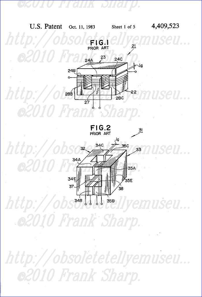
1. A pincushion distortion correction apparatus for television receivers comprising;
a saturable transformer including a ferromagnetic core forming a cubic magnetic loop path structure, said ferromagnetic core consisting of two ferromagnetic core pieces having four legs and two common portions, a controlled winding wound on the first and second ones of said four legs of the core, a control winding wound on the second and third ones of said four legs of the core, and a space gap means provided between said two ferromagnetic core pieces;
a deflection coil being connected in series with said controlled winding; and
a signal source for supplying a control parabolic signal to said control winding.
2. A pincushion distortion correction apparatus according to claim 1, wherein said two pieces constituting ferromagnetic core have respectively four legs and a common portion, and said space gap means is provided between the first and second legs of said two pieces of cores. 3. A pincushion distortion correction apparatus according to claim 1, wherein one piece of said ferromagnetic core has four legs and a common portion and the other core is a ferromagnetic core plate, and also wherein said space gap means is provided between the top of the first and second legs of said one core and said core plate. 4. A pincushion distortion correction apparatus for television receivers comprising;
a saturable transformer including a ferromagnetic core forming a cubic magnetic loop structure, said ferromagnetic core consisting of two core pieces and, said cubic magnetic loop having four magnetic legs and two common portions, a horizontal winding wound on the first and second legs of the core, a vertical winding wound on the second and third legs of the core, and a space gap means provided between said first and second legs of one of the ferromagnetic core pieces and the other core piece;
a horizontal deflection coil connected in series with said horizontal winding; and
a signal source for supplying a vertical parabolic signal to said vertical winding.
Description:
BACKGROUND OF THE INVENTION
1. Field of the Invention
This invention relates to pincushion distortion correction apparatus and, more particularly, to an apparatus to this end having a control coil and a controlled coil, these coils being coupled to a saturable magnetic core in a perpendicular relation to each other.
2. Description of the Prior Art
A prior-art saturable reactor apparatus for correcting pincushion distortion in a television receiver has a construction as shown in FIG. 1.
In the pincushion distortion correction transformer 21 shown in FIG. 1, saturable E and I type cores 22 and 23 are held in face to face relationship to each other with a predetermined gap l g provided between them, a control coil 27 is wound on a central leg 24 A of the E type core 22, and first and second controlled coils 28 B and 28 C are wound on the respective opposite end legs 24 B and 24 C of the same core such that they operate differentially with respect to each other. For correcting horizontal pincushion distortions, a parabolic current changing at the vertical scanning frequency is caused through the control coil 27 to modulate the horizontal deflecting current flowing through the controlled coils 28 B and 28 C , thus obtaining a correction such that the horizontal deflection current becomes maximum at the center of the vertical scanning portion. The inductance L H of the transformer 21 is given as ##EQU1## where N H1 and N H2 are respectively turns numbers of the first and second controlled coils 28 B and 28 C (N H1 =N H2 ), l is the average length of the magnetic path, S is the sectional area of the core, and μ e is the effective magnetic permeability while μO is the magnetic permeability of a vacuum.
FIG. 2 shows a pincushion distortion correction transformer disclosed in a earlier patent application filed by the same applicant, and it is mentioned here for the purpose of faccilitating the understanding of the present invention. In this transformer 31, a control coil 37 and a controlled coil 38 are wound in a perpendicular relation to each other on legs 34 and 35 of a pair of four leg cores 32 and 33. The core 32 has a square or rectangular plate-like base portion 34 E and four legs 34 A to 34 D extending from the four corners of the base portion. The four legs have equal sectional area. Likewise, the core 33 has a base portion 35 E and four legs 35 A to 35 D . In FIG. 2, the legs 34 D and 35 D are concealed and not shown. The cores 32 and 33 having this construction are held such that the ends of the legs 34 A to 34 D of the former are respectively brought into contact with the corresponding legs 35 A to 35 D of the latter through predetermined gaps to define a constant space l g . The control coil 37 is wound on the legs 34 B and 34 D of the core 32 as a set, and the controlled coil 38 is wound on the legs 35 A and 35 B of the core 33 as a set. The inductance of this perpendicular transformer 31 is given as ##EQU2## N H in equation (2) is the turns number of the controlled coil 38 having almost half the turns of FIG. 1, and this means that for the example in FIG. 2 substantially the same variable inductance characteristic can be obtained with one half the turns number compared with the prior-art example of FIG. 1.
However, these pincushion distortion correction saturable reactor apparatus shown in FIGS. 1 and 2, have disadvantages; for example, raster shrinkage occurs in the neighborhood of the center of the screen, and the horizontal linearity is inferior.
 FIG. 3 is a graph showing the variable inductance characteristic of the perpendicular transformer 31 shown in FIG. 2. In this graph, the abscissa represents the horizontal deflecting current I H (in A), and the ordinate represents the inductance L H (in μH). The vertical deflecting current I V (in mA) is taken as the parameter, and characteristic curves for 0,10,20,40 mA respectively are shown. When the inductance characteristic is as shown in FIG. 3, the reproduction on the screen has a character as shown in FIG. 4. The reproduction shown in FIG. 4 is obtained when a reference pattern consisting of a plurality of uniformly spaced vertical lines is reproduced on the television screen after the horizontal pincushion distortion correction using the transformer 31 mentioned above. The ratio of the interline space in the reproduction of FIG. 4 with respect to the interline average space in the reference pattern (in %) is as shown in FIG. 5. It will be seen that the raster shrinkage is produced in the neighborhood of the center of the screen, particularly in a horizontal deflecting current region between from -1 to +1 A. Due to this shrinkage, the horizontal linearity is inferior. Therefore the dynamic range of the variable inductance defined by the DC superimposition characteristics thereof becomes narrow.
SUMMARY OF THE INVENTION
The present invention seeks to overcome the aforementioned drawback inherent in the prior art, and its object is to provide a pincushion distortion correction saturable reactor apparatus, which is simple in construction and can improve the variable inductance characteristic and preclude the distortion of deflection in the neighborhood of the center of the reproduction, thus permitting wide improvement of the horizontal linearity and extension of the DC superimposition variable inductance dynamic range.
In accordance with an aspect of present invention, the apparatus for correcting pincushion distortion comprises a core having a gap, a control coil and a controlled coil, the control and controlled coils being wound on the core in a perpendicular relation to each other, the gap having an unbalanced configuration in the path of magnetic flux produced by the controlled coil, the control coil supplying a parabolic current for pincushion distortion correction, and the controlled coil supplying a deflecting current to be corrected.
The above and other objects, features and advantages of the illustrated embodiments of the invention will appear from the description given below, which is to be read in connection with the accompanying drawings.
BRIEF DESCRIPTION OF THE DRAWINGS
FIG. 1 is a perspective view showing a prior art example.
FIGS. 2 through 5 illustrate information concerning a transformer, given for the purpose of facilitating the understanding of the present invention, and of which FIG. 2 is a perspective view of the transformer;
FIG. 3 is a graph showing the variable inductance characteristic in FIG. 1 or 2;
FIG. 4 is a plan view showing the reproduction on a television screen in example FIG. 1 or 2;
FIG. 5 is a graph showing the horizontal linearity;
FIGS. 6 and 7 show a first embodiment of the present invention, and of which FIG. 6 is a perspective view showing the apparatus before the assembly, and FIG. 7 is a perspective view showing the apparatus after the assembly.
FIGS. 8 through 13 show a second embodiment of the present invention, and of which FIG. 8 is a perspective view showing the apparatus before the assembly thereof, FIG. 9 is a perspective view showing the apparatus after assembly, FIG. 10 is a fragmentary perspective view of the apparatus for illustrating the operation thereof, FIG. 11 is a graph showing the variable inductance characteristic, FIG. 12 is a plan view showing the reproduction on a television screen, and FIG. 13 is a graph showing the horizontal linearity.
DETAILED DESCRIPTION OF THE PREFERRED EMBODIMENTS
Now, a preferred embodiment of the present invention will be described in conjunction with some preferred embodiments thereof with reference to the accompanying drawings.
 FIGS. 6 and 7 show a first embodiment of the pincushion distortion correction saturable reactor apparatus 1 according to the present invention. FIG. 6 shows a perspective view of the apparatus before the assembly thereof, and FIG. 7 shows a perspective view of the apparatus after assembly. In these Figures, the apparatus comprises cores 2 and 3 having an identical shape and made of a ferrite material. The core 2 has a plate-like base portion 4 E , for instance having a square or rectangular shape, and four legs 4 A ,4 B ,4 C and 4 D perpendicularly projecting from the four corners of one side of the base portion and having an equal sectional area. Likewise, the other core 3 has a base portion 5 E and four leg portions 5 A ,5 B ,5 C and 5 D . These cores 2 and 3 are arranged such that the legs 4 A to 4 D of the former abut on the corresponding legs 5 A to 5 D of the latter. More particularly, an adjacent two of the four legs of the core 2, for instance legs 4 A and 4 B are coupled to the corresponding legs of the other core, for instance legs 5 A and 5 B via a spacer 6. Thus, the faces of the legs facing each other are inclined with respect to each other, and the gap is increased toward the reader. The thickness of the spacer 6 is set substantially to 2 l g , i.e., double the gap interval l g in the afore-mentioned prior-art construction. A control coil 7 is wound on a pair of legs, namely the leg 4 B of the core 2 in contact with the spacer 6 and the leg 4 D adjacent to the leg 4 B but not in contact with the spacer 6. A controlled coil 8 is wound on a pair of legs 5 A and 5 B of the other core 3 in contact with the spacer 6. Alternatively, the controlled coil 8 may be wound on pair legs 5 C and 5 D which are not in contact with the spacer 6. The magnetic flux produced by the current through the control coil 7 passes through a loop constituted by the legs 4 A and 5 A and legs 5 B and 4 B. The magnetic flux produced by the current through the controlled coil 8 passes through a loop constituted by the legs 4 A and 5 A and legs 5 C and 4 C . Since the facing faces of the individual pairs of legs constituting the path of magnetic flux set up by the controlled coil 8 are inclined due to the spacer 6 interposed between the legs 4 A and 5 A and also between the legs 4 B and 5 B , the gap between these facing surfaces is increased toward the reader in the FIG. 7, that is, the gap formed in the path of magnetic flux set up by the controlled coil 8 has an unbalanced form. In the afore-mentioned prior-art example (shown in FIG. 2), in which the facing surfaces of the individual pair legs are parallel, the gaps in the magnetic flux paths for both the control and controlled coils are balanced in form.
 FIGS. 8 through 10 show a second embodiment of the present invention. In this embodiment of the pincushion distortion correction saturable reactor apparatus 11, a pair of cores 12 and 13 which have different shapes are used. The assembled form of the pincushion distortion saturable reactor apparatus 11 is practially the same as the apparatus of the first embodiment, but this embodiment is different from the first embodiment in the position, in which the core halves of the apparatus are coupled to each other, and the assembly can be more readily made.
More particularly, referring to FIGS. 8 and 10, the core 12 has a base portion 14 E , for instance having a square or rectangular shape, and four legs 14 A ,14 B ,14 C and 14 D perpendicularly projecting from the four corners of the base portion and somewhat a greater length (capable of accommodating two coils). The core 13, on the other hand, consists of a square or rectangular plate corresponding to the base portion of cores in the first embodiment.
These cores 12 and 13 are arranged such that they abut on each other with a spacer 6 provided in contact with two adjacent legs 14 A and 14 B of the core 12 to form a gap of an unbalanced form for the controlled coil 8. The coil 7 is wound on the set of legs 14 B and 14 D , and the controlled coil 8 is wound on a set of legs 14 A and 14 B in contact with the spacer 6. In this construction, the gap in the magnetic flux path for the controlled coil 8 varies for different portions of the facing surfaces and thus has an unbalanced form.
In the use of the first and second embodiments for the lateral pincushion distortion correction, parabolic current I V containing an appropriate DC bias is supplied to the control coil 7, and horizontal deflecting current I H is supplied to the controlled coil 8. In this case, the turns number N V of the control coil 7 is selected relatively large to reduce the exciting current I V so that a flux φ V within a saturating region is produced by the magnetizing force N V I V . For the control coil 8 a large diameter wire is used, and its turns number N H is set to a value necessary for obtaining the required variable inductance for the lateral pincushion distortion correction.
The first and second embodiments having the above constructions according to the present invention operate practically in the same way, so the operation of the second embodiment only will be described.
The flux φ V produced by the current I V through the control coil 7 passes through the leg 14 B , base portion 14 E and leg 14 A of the core 12 and the core 13 as shown by dashed arrows in FIG. 9. Also, although not shown, a flux is caused to pass through the leg 14 D , base portion 14 E and 14 C of the core 12 and core 13. On the other hand, the flux φ H produced by the current I H through the controlled coil 8 passes through a loop constituted by the leg 14 A , base portion 14 E and leg 14 C of the core 12 and the core 13 as shown by solid arrows in FIG. 9. These fluxes φ V and φ H do not link with each other, so that no induction voltage is produced. Thus, by causing a parabolic current at the vertical scanning frequency to flow through the control coil 7, the inductance of the controlled coil 8 can be varied to obtain the correction of the lateral pincushion distortion.
Now, the effects of the gap having the unbalanced form will be described. In a state when the magnetomotive force N V I V provided by the control coil 7 is less than the magnetomotive force N H I H provided by the controlled coil 8 (i.e., N V I V H I H ), the flux through the four legs 14 A to 14 D , and hence the magnetic permeability, is controlled by the magnetomotive force N H I H . Thus, in the neighborhood of the end faces of the legs 14 C and 14 D free from the spacer 6, the magnetic saturation in the core sets gradually in from the contact points of the legs 14 C and 14 D with the core 13, and substantially the similar variable inductance characteristic as that obtained with the balanced gap perpendicular transformer 31 shown in FIG. 2 can be obtained.
On the other hand, in a state when the magnetomotive force N V I V is greater than the magnetomotive force N H I H (i.e., N V I H >N H I H ), the saturation of the core in the neighborhood of the gaps defined by the end faces of the legs 14 C and 14 D is determined by the magnetomotive force N V I V . For the flux φ V , most flux flows in one loop through the legs 14 C and 14 D , because the other magnetic loop which includes the legs 14 A and 14 B has two wide gaps, therefore the magnetic reluctance of this loop is larger than that of the former. Therefore the large flux φ V concentrates at the contact points of the legs 14 C and 14 D . The concentration of flux makes the points saturate and, the saturated points act as the effective gaps. With the saturation in the neighborhood of the gaps defined by the legs 14 C and 14 D , the magnetic reluctance of the gaps is apparently increased. Also, the distance of the gap in the magnetic flux path for the controlled coil 8 is increased in the gaps defined by the legs 14 C and 14 D . The flux φ H and the apparent gap Δl g are shown in FIG. 10.
 With the apparent increase of the magnetic reluctance (i.e., increase of the gap distance), the inductance is reduced to L H , which is expressed as ##EQU3## where l is the average length of magnetic path, S is the sectional area of the core, and μ e is the effective permeability, while μ O is the permeability of a vacuum.
FIG. 11 shows the variable inductance characteristics of the pincushion distortion correction saturable reactor apparatus having the above construction. In the graph of FIG. 11, the ordinate is taken as the variable inductance L H ' in μH, and the abscissa is taken as the horizontal deflecting current I H in A. Characteristic curves shown are obtained when the vertical parabolic current I V is respectively 0,10,20 and 40 mA. These characteristic curves have substantially M-shaped forms with the variable inductance L H , reduced in an I H range in the neighborhood of 0 corresponding to the central portion of the screen. Thus, in the reproduction, the deflectional distortion in the central portion of the television screen can be widely improved as shown in FIG. 12. FIG. 12 is similar to FIG. 4, showing the reproduction of a reference pattern consisting of uniformly spaced vertical lines. In this case, extremely improved horizontal linearity compared with that shown in FIG. 5 can be obtained as shown in FIG. 13. Also, the dynamic range for the control coil current I V and controlled coil current I H can be increased. Further, with the same outer case size and current I H , a larger CRT size correction is possible even with a reduced value of current I V . Furthermore, with the same amplitude of control current, a larger CRT where the horizontal deflecting current is higher is possible to correct.
The characteristics of the prior-art reactor apparatus of FIG. 1, as shown in FIGS. 3 through 5, and the characteristics of the reactor apparatus according to the present invention, as shown in FIGS. 11 through 13, are based upon data obtained from experiments using a 20-inch color television receiver with a deflection angle of 100 degrees for 10% pincushion distortion correction. The relevant conditions and performance are shown in table 1.
A signal source means S is indicated in FIG. 7 for supplying a control parabolic signal to the control winding 7, and a deflection coil means D is indicated in FIG. 7 as being connected in series with the controlled winding 8, for the sake of diagrammatic illustration.
The data listed in Table 1 for the present invention are for the second embodiment. According to the present invention, the volume of the apparatus can be reduced to 0.58 times that of the prior-art apparatus. Also, the total weight can be reduced to 0.66 times that in the case of the prior art. Further, in the performance, the horizontal linearity can be improved, and the heat dissipation of the core can be reduced.
As has been described in the foregoing, with the pincushion distortion correction saturable reactor apparatus according to the present invention, which is a saturable transformer comprising a core having four legs and respective common portions (such as 4E, 5E, FIG. 7, and 13, 14E, FIG. 9), and controlled and control coils coupled to the core legs in a perpendicular relation to each other, the core gap for the controlled coil is provided in an unbalanced form, and a parabolic current at the vertical scanning frequency (or at horizontal scanning frequency) containing a superimposed DC component is caused, through the control coil, thus modulating the inductance of the controlled coil.
By the unbalance of the gap is meant that the gap distance varies with different portions of the facing surfaces defining the gap. This can be obtained by interposing a spacer between two of the four legs on which the controlled coil is wound as mentioned above or between the other two legs so that the surfaces forming the gap are inclined with respect to each other.
With this construction, the variable inductance is reduced in a region in which the magnetomotive force produced by the control coil is greater than that produced by the controlled coil and, as a whole, characteristic curves having M-shaped forms can be obtained. Thus, the deflectional distortion in the neighborhood of the center of the reproduction on the screen is reduced, so that horizontal linearity can be widely improved. In addition, the dynamic range of the variable inductance inclusive of the superimposed DC portion is extended, so that it is possible to obtain size reduction and wide cost reduction compared with the prior art. Further, it is possible to realize the reduction of heat dissipation of the core, reduction of the controlled power, reduction of the number of component parts connected to the transformer and also reduction of the area of the printed circuit board occupied by the transformer.
The above embodiments of the present invention are by no means limitative, and the invention may be applied to the top and bottom pincushion distortion correction as well. Also, various other changes and modifications are possible without departing from the scope and spirit of the present invention.
SONY DST EHT FBT TRANSFORMER Bobbin structure for high voltage transformers EHT Output.
A coil bobbin for a fly-back transformer or the like having a bobbin proper. A plurality of partition members or flanges are formed on the bobbin proper with a slot between adjacent ones. At least first and second coil units are formed in the bobbin proper, each having several slots, formed between the flanges, and first and second high voltage coils are wound on the first and second coil units in opposite directions, respectively. A rectifying means is connected in series to the first and second coil units, and a cut-off portion or recess is provided on each of the partition members. In this case, a wire lead of the coil units passes from one slot to an adjacent slot through the cut-off portion which is formed as a delta groove, and one side of the delta groove is corresponded to the tangent direction to the winding direction.

1. A fly-back transformer comprising a coil bobbin comprising a plurality of parallel spaced discs with a first adjacent plurality of said disc formed with delta shaped slots having first edges which extend tangentially to a first winding direction and a first winding wound on said first adjacent plurality of said discs in said first winding direction, a second adjacent plurality of said discs formed with delta shaped slots having first edges which extend tangentially to a second winding direction opposite said first winding direction and a second winding wound on said second adjacent plurality of said discs in said second winding direction, a third adjacent plurality of said discs formed with delta shaped slots having first edges which extend tangentially to said first winding direction and a third winding wound on said third adjacent plurality of said discs in said first winding direction and said second plurality of adjacent discs mounted between said first and third plurality of adjacent discs. 2. A fly-back transformer according to claim 1 wherein adjacent ones of said first adjacent plurality of discs are mounted such that their delta shaped slots are orientated 180 degrees relative to each other. 3. A fly-back transformer according to claim 2 including a first winding turning partition mounted between said first and second adjacent plurality of discs and formed with grooves and notches for changing winding direction between said first and second windings and a second winding turning partition mounted between said second and third adjacent plurality of discs and formed with grooves and notches for changing the winding direction between said second and third windings. 4. A fly-back transformer according to claim 3 wherein said first and second winding turning partitions are formed with winding guiding slots for guiding the winding between the first, second and third adjacent plurality of discs. 5. A fly-back transformer according to claim 2 including a first rectifying means connected between one end of said first winding and one end of said second winding, and a second rectifying means connected between the second end of said second winding and one end of said third winding. 6. A fly-back transformer according to claim 5 wherein the second end of said first winding is grounded and a third rectifying means connected between the second end of said third winding and an output terminal.
1. Field of the Invention
This invention relates to pincushion distortion correction apparatus and, more particularly, to an apparatus to this end having a control coil and a controlled coil, these coils being coupled to a saturable magnetic core in a perpendicular relation to each other.
2. Description of the Prior Art
A prior-art saturable reactor apparatus for correcting pincushion distortion in a television receiver has a construction as shown in FIG. 1.
In the pincushion distortion correction transformer 21 shown in FIG. 1, saturable E and I type cores 22 and 23 are held in face to face relationship to each other with a predetermined gap l g provided between them, a control coil 27 is wound on a central leg 24 A of the E type core 22, and first and second controlled coils 28 B and 28 C are wound on the respective opposite end legs 24 B and 24 C of the same core such that they operate differentially with respect to each other. For correcting horizontal pincushion distortions, a parabolic current changing at the vertical scanning frequency is caused through the control coil 27 to modulate the horizontal deflecting current flowing through the controlled coils 28 B and 28 C , thus obtaining a correction such that the horizontal deflection current becomes maximum at the center of the vertical scanning portion. The inductance L H of the transformer 21 is given as ##EQU1## where N H1 and N H2 are respectively turns numbers of the first and second controlled coils 28 B and 28 C (N H1 =N H2 ), l is the average length of the magnetic path, S is the sectional area of the core, and μ e is the effective magnetic permeability while μO is the magnetic permeability of a vacuum. FIG. 2 shows a pincushion distortion correction transformer disclosed in a earlier patent application filed by the same applicant, and it is mentioned here for the purpose of faccilitating the understanding of the present invention. In this transformer 31, a control coil 37 and a controlled coil 38 are wound in a perpendicular relation to each other on legs 34 and 35 of a pair of four leg cores 32 and 33. The core 32 has a square or rectangular plate-like base portion 34 E and four legs 34 A to 34 D extending from the four corners of the base portion. The four legs have equal sectional area. Likewise, the core 33 has a base portion 35 E and four legs 35 A to 35 D . In FIG. 2, the legs 34 D and 35 D are concealed and not shown. The cores 32 and 33 having this construction are held such that the ends of the legs 34 A to 34 D of the former are respectively brought into contact with the corresponding legs 35 A to 35 D of the latter through predetermined gaps to define a constant space l g . The control coil 37 is wound on the legs 34 B and 34 D of the core 32 as a set, and the controlled coil 38 is wound on the legs 35 A and 35 B of the core 33 as a set. The inductance of this perpendicular transformer 31 is given as ##EQU2## N H in equation (2) is the turns number of the controlled coil 38 having almost half the turns of FIG. 1, and this means that for the example in FIG. 2 substantially the same variable inductance characteristic can be obtained with one half the turns number compared with the prior-art example of FIG. 1.
However, these pincushion distortion correction saturable reactor apparatus shown in FIGS. 1 and 2, have disadvantages; for example, raster shrinkage occurs in the neighborhood of the center of the screen, and the horizontal linearity is inferior.
 FIG. 3 is a graph showing the variable inductance characteristic of the perpendicular transformer 31 shown in FIG. 2. In this graph, the abscissa represents the horizontal deflecting current I H (in A), and the ordinate represents the inductance L H (in μH). The vertical deflecting current I V (in mA) is taken as the parameter, and characteristic curves for 0,10,20,40 mA respectively are shown. When the inductance characteristic is as shown in FIG. 3, the reproduction on the screen has a character as shown in FIG. 4. The reproduction shown in FIG. 4 is obtained when a reference pattern consisting of a plurality of uniformly spaced vertical lines is reproduced on the television screen after the horizontal pincushion distortion correction using the transformer 31 mentioned above. The ratio of the interline space in the reproduction of FIG. 4 with respect to the interline average space in the reference pattern (in %) is as shown in FIG. 5. It will be seen that the raster shrinkage is produced in the neighborhood of the center of the screen, particularly in a horizontal deflecting current region between from -1 to +1 A. Due to this shrinkage, the horizontal linearity is inferior. Therefore the dynamic range of the variable inductance defined by the DC superimposition characteristics thereof becomes narrow.
 SUMMARY OF THE INVENTION
The present invention seeks to overcome the aforementioned drawback inherent in the prior art, and its object is to provide a pincushion distortion correction saturable reactor apparatus, which is simple in construction and can improve the variable inductance characteristic and preclude the distortion of deflection in the neighborhood of the center of the reproduction, thus permitting wide improvement of the horizontal linearity and extension of the DC superimposition variable inductance dynamic range.
In accordance with an aspect of present invention, the apparatus for correcting pincushion distortion comprises a core having a gap, a control coil and a controlled coil, the control and controlled coils being wound on the core in a perpendicular relation to each other, the gap having an unbalanced configuration in the path of magnetic flux produced by the controlled coil, the control coil supplying a parabolic current for pincushion distortion correction, and the controlled coil supplying a deflecting current to be corrected.
The above and other objects, features and advantages of the illustrated embodiments of the invention will appear from the description given below, which is to be read in connection with the accompanying drawings.
BRIEF DESCRIPTION OF THE DRAWINGS
FIG. 1 is a perspective view showing a prior art example.
FIGS. 2 through 5 illustrate information concerning a transformer, given for the purpose of facilitating the understanding of the present invention, and of which FIG. 2 is a perspective view of the transformer;
FIG. 3 is a graph showing the variable inductance characteristic in FIG. 1 or 2;
FIG. 4 is a plan view showing the reproduction on a television screen in example FIG. 1 or 2;
FIG. 5 is a graph showing the horizontal linearity;
FIGS. 6 and 7 show a first embodiment of the present invention, and of which FIG. 6 is a perspective view showing the apparatus before the assembly, and FIG. 7 is a perspective view showing the apparatus after the assembly.
FIGS. 8 through 13 show a second embodiment of the present invention, and of which FIG. 8 is a perspective view showing the apparatus before the assembly thereof, FIG. 9 is a perspective view showing the apparatus after assembly, FIG. 10 is a fragmentary perspective view of the apparatus for illustrating the operation thereof, FIG. 11 is a graph showing the variable inductance characteristic, FIG. 12 is a plan view showing the reproduction on a television screen, and FIG. 13 is a graph showing the horizontal linearity.
DETAILED DESCRIPTION OF THE PREFERRED EMBODIMENTS
Now, a preferred embodiment of the present invention will be described in conjunction with some preferred embodiments thereof with reference to the accompanying drawings.
 FIGS. 6 and 7 show a first embodiment of the pincushion distortion correction saturable reactor apparatus 1 according to the present invention. FIG. 6 shows a perspective view of the apparatus before the assembly thereof, and FIG. 7 shows a perspective view of the apparatus after assembly. In these Figures, the apparatus comprises cores 2 and 3 having an identical shape and made of a ferrite material. The core 2 has a plate-like base portion 4 E , for instance having a square or rectangular shape, and four legs 4 A ,4 B ,4 C and 4 D perpendicularly projecting from the four corners of one side of the base portion and having an equal sectional area. Likewise, the other core 3 has a base portion 5 E and four leg portions 5 A ,5 B ,5 C and 5 D . These cores 2 and 3 are arranged such that the legs 4 A to 4 D of the former abut on the corresponding legs 5 A to 5 D of the latter. More particularly, an adjacent two of the four legs of the core 2, for instance legs 4 A and 4 B are coupled to the corresponding legs of the other core, for instance legs 5 A and 5 B via a spacer 6. Thus, the faces of the legs facing each other are inclined with respect to each other, and the gap is increased toward the reader. The thickness of the spacer 6 is set substantially to 2 l g , i.e., double the gap interval l g in the afore-mentioned prior-art construction. A control coil 7 is wound on a pair of legs, namely the leg 4 B of the core 2 in contact with the spacer 6 and the leg 4 D adjacent to the leg 4 B but not in contact with the spacer 6. A controlled coil 8 is wound on a pair of legs 5 A and 5 B of the other core 3 in contact with the spacer 6. Alternatively, the controlled coil 8 may be wound on pair legs 5 C and 5 D which are not in contact with the spacer 6. The magnetic flux produced by the current through the control coil 7 passes through a loop constituted by the legs 4 A and 5 A and legs 5 B and 4 B. The magnetic flux produced by the current through the controlled coil 8 passes through a loop constituted by the legs 4 A and 5 A and legs 5 C and 4 C . Since the facing faces of the individual pairs of legs constituting the path of magnetic flux set up by the controlled coil 8 are inclined due to the spacer 6 interposed between the legs 4 A and 5 A and also between the legs 4 B and 5 B , the gap between these facing surfaces is increased toward the reader in the FIG. 7, that is, the gap formed in the path of magnetic flux set up by the controlled coil 8 has an unbalanced form. In the afore-mentioned prior-art example (shown in FIG. 2), in which the facing surfaces of the individual pair legs are parallel, the gaps in the magnetic flux paths for both the control and controlled coils are balanced in form.
  FIGS. 8 through 10 show a second embodiment of the present invention. In this embodiment of the pincushion distortion correction saturable reactor apparatus 11, a pair of cores 12 and 13 which have different shapes are used. The assembled form of the pincushion distortion saturable reactor apparatus 11 is practially the same as the apparatus of the first embodiment, but this embodiment is different from the first embodiment in the position, in which the core halves of the apparatus are coupled to each other, and the assembly can be more readily made.
 More particularly, referring to FIGS. 8 and 10, the core 12 has a base portion 14 E , for instance having a square or rectangular shape, and four legs 14 A ,14 B ,14 C and 14 D perpendicularly projecting from the four corners of the base portion and somewhat a greater length (capable of accommodating two coils). The core 13, on the other hand, consists of a square or rectangular plate corresponding to the base portion of cores in the first embodiment.
These cores 12 and 13 are arranged such that they abut on each other with a spacer 6 provided in contact with two adjacent legs 14 A and 14 B of the core 12 to form a gap of an unbalanced form for the controlled coil 8. The coil 7 is wound on the set of legs 14 B and 14 D , and the controlled coil 8 is wound on a set of legs 14 A and 14 B in contact with the spacer 6. In this construction, the gap in the magnetic flux path for the controlled coil 8 varies for different portions of the facing surfaces and thus has an unbalanced form.
In the use of the first and second embodiments for the lateral pincushion distortion correction, parabolic current I V containing an appropriate DC bias is supplied to the control coil 7, and horizontal deflecting current I H is supplied to the controlled coil 8. In this case, the turns number N V of the control coil 7 is selected relatively large to reduce the exciting current I V so that a flux φ V within a saturating region is produced by the magnetizing force N V I V . For the control coil 8 a large diameter wire is used, and its turns number N H is set to a value necessary for obtaining the required variable inductance for the lateral pincushion distortion correction.
The first and second embodiments having the above constructions according to the present invention operate practically in the same way, so the operation of the second embodiment only will be described.
The flux φ V produced by the current I V through the control coil 7 passes through the leg 14 B , base portion 14 E and leg 14 A of the core 12 and the core 13 as shown by dashed arrows in FIG. 9. Also, although not shown, a flux is caused to pass through the leg 14 D , base portion 14 E and 14 C of the core 12 and core 13. On the other hand, the flux φ H produced by the current I H through the controlled coil 8 passes through a loop constituted by the leg 14 A , base portion 14 E and leg 14 C of the core 12 and the core 13 as shown by solid arrows in FIG. 9. These fluxes φ V and φ H do not link with each other, so that no induction voltage is produced. Thus, by causing a parabolic current at the vertical scanning frequency to flow through the control coil 7, the inductance of the controlled coil 8 can be varied to obtain the correction of the lateral pincushion distortion.
Now, the effects of the gap having the unbalanced form will be described. In a state when the magnetomotive force N V I V provided by the control coil 7 is less than the magnetomotive force N H I H provided by the controlled coil 8 (i.e., N V I V H I H ), the flux through the four legs 14 A to 14 D , and hence the magnetic permeability, is controlled by the magnetomotive force N H I H . Thus, in the neighborhood of the end faces of the legs 14 C and 14 D free from the spacer 6, the magnetic saturation in the core sets gradually in from the contact points of the legs 14 C and 14 D with the core 13, and substantially the similar variable inductance characteristic as that obtained with the balanced gap perpendicular transformer 31 shown in FIG. 2 can be obtained.
 With the apparent increase of the magnetic reluctance (i.e., increase of the gap distance), the inductance is reduced to L H , which is expressed as ##EQU3## where l is the average length of magnetic path, S is the sectional area of the core, and μ e is the effective permeability, while μ O is the permeability of a vacuum.
 FIG. 11 shows the variable inductance characteristics of the pincushion distortion correction saturable reactor apparatus having the above construction. In the graph of FIG. 11, the ordinate is taken as the variable inductance L H ' in μH, and the abscissa is taken as the horizontal deflecting current I H in A. Characteristic curves shown are obtained when the vertical parabolic current I V is respectively 0,10,20 and 40 mA. These characteristic curves have substantially M-shaped forms with the variable inductance L H , reduced in an I H range in the neighborhood of 0 corresponding to the central portion of the screen. Thus, in the reproduction, the deflectional distortion in the central portion of the television screen can be widely improved as shown in FIG. 12. FIG. 12 is similar to FIG. 4, showing the reproduction of a reference pattern consisting of uniformly spaced vertical lines. In this case, extremely improved horizontal linearity compared with that shown in FIG. 5 can be obtained as shown in FIG. 13. Also, the dynamic range for the control coil current I V and controlled coil current I H can be increased. Further, with the same outer case size and current I H , a larger CRT size correction is possible even with a reduced value of current I V . Furthermore, with the same amplitude of control current, a larger CRT where the horizontal deflecting current is higher is possible to correct.
The characteristics of the prior-art reactor apparatus of FIG. 1, as shown in FIGS. 3 through 5, and the characteristics of the reactor apparatus according to the present invention, as shown in FIGS. 11 through 13, are based upon data obtained from experiments using a 20-inch color television receiver with a deflection angle of 100 degrees for 10% pincushion distortion correction. The relevant conditions and performance are shown in table 1.
A signal source means S is indicated in FIG. 7 for supplying a control parabolic signal to the control winding 7, and a deflection coil means D is indicated in FIG. 7 as being connected in series with the controlled winding 8, for the sake of diagrammatic illustration.
| TABLE 1 |
| ______________________________________ |
| Present Item Invention Prior Art |
| ______________________________________ |
Core Data Gap 75μ (unbalanced) 38 (balanced) N V /N H (turns ratio) 1200 T /16 T 900 T /9 T + 9 T Outer dimensions 18 × 18 × 22 mm 19 × 21.5 × 30 mm of core Volume of core 4608 mm 3 9747 mm 3 Total weight 38.5 g 58.5 g Performance Horizontal linearity +1.4%.about.-2.7% +6.3%.about.-5.7% Controlled power 0.6 W 0.8 W Heat generation 20° C. 30° C. from core |
| ______________________________________ |
As has been described in the foregoing, with the pincushion distortion correction saturable reactor apparatus according to the present invention, which is a saturable transformer comprising a core having four legs and respective common portions (such as 4E, 5E, FIG. 7, and 13, 14E, FIG. 9), and controlled and control coils coupled to the core legs in a perpendicular relation to each other, the core gap for the controlled coil is provided in an unbalanced form, and a parabolic current at the vertical scanning frequency (or at horizontal scanning frequency) containing a superimposed DC component is caused, through the control coil, thus modulating the inductance of the controlled coil.
By the unbalance of the gap is meant that the gap distance varies with different portions of the facing surfaces defining the gap. This can be obtained by interposing a spacer between two of the four legs on which the controlled coil is wound as mentioned above or between the other two legs so that the surfaces forming the gap are inclined with respect to each other.
With this construction, the variable inductance is reduced in a region in which the magnetomotive force produced by the control coil is greater than that produced by the controlled coil and, as a whole, characteristic curves having M-shaped forms can be obtained. Thus, the deflectional distortion in the neighborhood of the center of the reproduction on the screen is reduced, so that horizontal linearity can be widely improved. In addition, the dynamic range of the variable inductance inclusive of the superimposed DC portion is extended, so that it is possible to obtain size reduction and wide cost reduction compared with the prior art. Further, it is possible to realize the reduction of heat dissipation of the core, reduction of the controlled power, reduction of the number of component parts connected to the transformer and also reduction of the area of the printed circuit board occupied by the transformer.
The above embodiments of the present invention are by no means limitative, and the invention may be applied to the top and bottom pincushion distortion correction as well. Also, various other changes and modifications are possible without departing from the scope and spirit of the present invention.
SONY DST EHT FBT TRANSFORMER Bobbin structure for high voltage transformers EHT Output.
A coil bobbin for a fly-back transformer or the like having a bobbin proper. A plurality of partition members or flanges are formed on the bobbin proper with a slot between adjacent ones. At least first and second coil units are formed in the bobbin proper, each having several slots, formed between the flanges, and first and second high voltage coils are wound on the first and second coil units in opposite directions, respectively. A rectifying means is connected in series to the first and second coil units, and a cut-off portion or recess is provided on each of the partition members. In this case, a wire lead of the coil units passes from one slot to an adjacent slot through the cut-off portion which is formed as a delta groove, and one side of the delta groove is corresponded to the tangent direction to the winding direction.
1. A fly-back transformer comprising a coil bobbin comprising a plurality of parallel spaced discs with a first adjacent plurality of said disc formed with delta shaped slots having first edges which extend tangentially to a first winding direction and a first winding wound on said first adjacent plurality of said discs in said first winding direction, a second adjacent plurality of said discs formed with delta shaped slots having first edges which extend tangentially to a second winding direction opposite said first winding direction and a second winding wound on said second adjacent plurality of said discs in said second winding direction, a third adjacent plurality of said discs formed with delta shaped slots having first edges which extend tangentially to said first winding direction and a third winding wound on said third adjacent plurality of said discs in said first winding direction and said second plurality of adjacent discs mounted between said first and third plurality of adjacent discs. 2. A fly-back transformer according to claim 1 wherein adjacent ones of said first adjacent plurality of discs are mounted such that their delta shaped slots are orientated 180 degrees relative to each other. 3. A fly-back transformer according to claim 2 including a first winding turning partition mounted between said first and second adjacent plurality of discs and formed with grooves and notches for changing winding direction between said first and second windings and a second winding turning partition mounted between said second and third adjacent plurality of discs and formed with grooves and notches for changing the winding direction between said second and third windings. 4. A fly-back transformer according to claim 3 wherein said first and second winding turning partitions are formed with winding guiding slots for guiding the winding between the first, second and third adjacent plurality of discs. 5. A fly-back transformer according to claim 2 including a first rectifying means connected between one end of said first winding and one end of said second winding, and a second rectifying means connected between the second end of said second winding and one end of said third winding. 6. A fly-back transformer according to claim 5 wherein the second end of said first winding is grounded and a third rectifying means connected between the second end of said third winding and an output terminal.
Description:
BACKGROUND OF THE INVENTION
1. Field of the Invention
The present invention relates generally to a bobbin structure for high voltage transformers, and is directed more particularly to a bobbin structure for high voltage transformer suitable for automatically winding coils thereon.
2. Description of the Prior Art
In the art, when a wire lead is reversely wound on a bobbin separately at every winding block, a boss is provided at every winding block and the wire lead is wound on one block, then one end of the wire lead is tied to the boss where it will be cut off. The end of the wire lead is tied to another boss, and then the wire lead is wound in the opposite direction. Therefore, the prior art winding method requires complicated procedures and the winding of the wire lead cannot be rapidly done and also the winding can not be performed automatically. Further, the goods made by the prior art method are rather unsatisfactory and have a low yield.
OBJECTS AND SUMMARY OF THE INVENTION
Accordingly an object of the invention is to provide a coil bobbin for a fly-back transformer or the like by which a wire lead can be automatically wound on winding blocks of the coil bobbin even though the winding direction is different among the different winding blocks.
Another object of the invention is to provide a coil bobbin for a fly-back transformer or the like in which a bridge member and an inverse engaging device for transferring a wire lead from one wiring block to an adjacent wiring block of the coil bobbin and wiring the wire lead in opposite wiring directions between adjacent wiring blocks, and a guide member for positively guiding the wire lead are provided.
According to an aspect of the present invention, a coil bobbin for a fly-back transformer or the like is provided which comprises a plurality of partition members forming a plurality of slots, a first coil unit having several slots on which a first high voltage coil is wound in one winding direction, a second coil unit having several slots on which a second high voltage coil is wound in the other direction, a rectifying means connected in series to the first and second coil units, and a cut-off portion provided on each of the partition members, a wire lead passing from one slot to an adjacent slot through the cut-off portions, each of the cut-off portions being formed as a delta groove, and one side of the delta groove corresponding to a tangent to the winding direction.
The other objects, features and advantages of the present invention will become apparent from the following description taken in conjunction with the accompanying drawings through which the like reference numerals and letters designate the same elements and parts, respectively.
BRIEF DESCRIPTION OF THE DRAWINGS
FIG. 1 is a schematic diagram showing the construction of a fly-back transformer;
FIG. 2 is a connection diagram showing an example of the electrical connection of the fly-back transformer shown in FIG. 1;
FIG. 3 is a schematic diagram showing an example of a device for automatically winding a wire lead of the fly-back transformer on its bobbin;
FIG. 4 is a perspective view showing an example of the coil bobbin according to the present invention;
FIG. 5 is a plan view of FIG. 4;
FIGS. 6 and 7 are views used for explaining recesses or cut-off portions shown in FIGS. 4 and 5; and FIGS. 8A and 8B cross-sectional views showing an example of the inverse engaging means according to the present invention.
DESCRIPTION OF THE PREFERRED EMBODIMENT
When the high voltage winding of a fly-back transformer used in a high voltage generating circuit of a television receiver is divided into plural ones and then wound on a bobbin, the divided windings (divided coils) are connected in serie s through a plurality of rectifying diodes.
When the winding is divided into, for example, three portions, such as divided coils La, Lb and Lc, they are wound on a bobbin proper 1 from, for example, left to right sequentially in this order as shown in FIG. 1. In this case, if the divided coils La and Lc are selected to have the same sense of turn and the middle coil Lb is selected to have the opposite sense of turn from the coils La and Lc, the distance between the terminal end of coil La and the start of coil Lb and the distance between the terminal end of coil Lb and the start of coil Lc can be got relatively long. Therefore, diodes Da and Db can be mounted by utilizing the space above the block on which the middle coil Lb is wound as shown in FIG. 1, so that it becomes useless to provide spaces for diodes between the divided coils La and Lb and between the divided coils Lb and Lc and hence the bobbin proper 1 can be made compact.
FIG. 2 is a connection diagram showing the connection of the above fly-back transformer. In FIG. 2, reference numeral 2 designates a primary winding (Primary coil) of the fly-back transformer, reference letter L designates its high voltage winding (secondary coil), including divided coils La, Lb and Lc, 3 an output terminal, and 4 a lead wire connected to the anode terminal of a cathode ray tube (not shown), respectively.
An example of the bobbin structure according to the invention, which is suitable to automatically wind coils, which are different in sense of turn in each winding block as shown in FIG. 1, on the bobbin, will be hereinafter described with reference to the drawings.
FIG. 3 is a diagram showing an automatic winding apparatus of a wire lead on a coil bobbin. If it is assumed that the wire lead is wound in the order of w inding blocks A, B and C in FIG. 1 and the wire lead is wound on the block A with the bobbin proper 1 being rotated in the counter-clockwise direction as shown in FIG. 3, the relation between the bobbin proper 1 and the wire lead becomes as shown in FIG. 3. In this figure, reference numeral 6 designates a bobbin for feeding the wire lead.
Turning to FIG. 4, an example 10 of the bobbin structure or coil bobbin according to the present invention will be described now. In this example, the winding blocks A, B and C for the divided coils La, Lb and Lc are respectively divided into plural slots or sections by plural partition members or flanges 11, and a cut-off portion or recess 12 is formed on each of the flanges 11 through which the wire lead in one section is transferred to the following winding section.
As shown in FIG. 6, each recess 12 is so formed that its one side extends in the direction substantially coincident with the tangent to the circle of the bobbin proper 1 and its direction is selected in response to the sense of turn of the winding or wire lead. In this case, the direction of recess 12 means the direction of the opening of recess 12, and the direction of recess 12 is selected opposite to the sense of turn of the wi nding in the present invention.
Now, recesses 12A, which are formed in the winding block A, will be now described by way of example. The positions of recesses 12A formed on an even flange 11Ae and an odd flange 11A 0 are different, for example, about 180° as shown in FIGS. 6A and 6B. Since the bobbin proper 1 is rotated in the counter-clockwise direction in the winding block A and hence the sense of turn of the wire lead is in the clockwise direction, the recess 12A is formed on the even flange 11Ae at the position shown in FIG. 6A. That is, the direction of recess 12A is inclined with respect to the rotating direction of bobbin proper 1 as shown in FIG. 6A. In this case, one side 13a of recess 12A is coincident with the tangent to the circle of bobbin proper 1, while the other side 13b of recess 12A is selected to have an oblique angle with respect to the side 13a so that the recess 12A has a predetermined opening angle.
The opening angle of recess 12A is important but the angle between the side 13a of recess 12A and the tangent to the circle of bobbin proper 1 is also important in the invention. When the wire lead is bridged or transferred from one section to the following section through the recess 12A, the wire lead in one section advances to the following section in contact with the side 13a of recess 12A since the bobbin proper 1 is rotated. In the invention, if the side 13a of recess 12A is selected to be extended in the direction coincident with the tangent to the circle of bobbin proper 1, the wire lead can smoothly advance from one section to the next section without being bent.
In the invention, since the middle divided coil Lb is wound opposite to the divided coil La, a recess 12B provided on each of flanges 11B of the winding block B is formed to have an opening opposite to that of recess 12A formed in the winding block A as shown in FIGS. 6C and 6D.
As shown in FIG. 5, terminal attaching recesses 14 are provided between the winding blocks A and B to which diodes are attached respectively. In the illustrated example of FIG. 5, a flange 15AB is formed between the flanges 11A 0 and 11B 0 of winding blocks A and B, and the recesses 14 are formed between the flanges 11A 0 and 15AB and between 15AB and 11B 0 at predetermined positions. Then, terminal plates 16, shown in FIG. 4, are inserted into the recesses 14 and then fixed there to, respectively. The terminal plates 16 are not shown in FIG. 5. Between the winding blocks B and C and between the blocks A and B, similar terminal attaching recesses 14 are formed, and terminal plates 16 are also inserted thereinto and then fixed thereto.
As described above, since the divided coil Lb is wound opposite to the divided coils La and Lc, it is necessary that the winding direction of the wire lead be changed when the wire lead goes from the block A to block B and also from the block B to block C, respectively.
Turning to FIG. 7, an example of the winding or wire lead guide means according to the present invention will be now described. In FIG. 7, there are mainly shown a bridge member for the wire lead and an inve rse member or means for the wire lead which are provided between the winding blocks A and B. At first, a bridge means 20 and its guide means 21, which form the bridge member, will be described. The bridge means 20 is provided by forming a cut-out portion or recess in the middle flange 15AB located between the winding blocks A and B. In close relation to the bridge means or recess 20, the guide means 21 is provided on a bridge section X A at the side of block A. This guide means 21 is formed as a guide piece which connects an edge portion 20a of recess 20 at the winding direction side to the flange 11A 0 of block A in the oblique direction along the winding direction through the section X A .
Next, an inverse engaging means 22 will be now described with reference to FIGS. 7 and 8. If the flange 11B 0 of FIG. 7 is viewed from the right side, the inverse engaging means 22 can be shown in FIG. 8A. In this case, the tip end of one side 13a of recess 12B 1 is formed as a projection which is extended outwards somewhat beyond the outer diameter of flange 11B 0 . The inverse engaging means 22 may take any configuration but it is necessary that when the rotating direction of the bobbin proper 1 is changed to the clockwise direction, the wire lead can be engaged with the recess 12B 1 or projection of one side 13a and then suitably transferred to the next station.
Another guide means 23 is provided on a bridge section X B at the side of winding block B in close relation to the inverse engaging means 22. The guide means 23 is formed as a guide surface which is a projected surface from the bottom surface of section X B and extended obliquely in the winding direction. This guide means or guide surface 23 is inclinded low into the means 22 and has an edge 23a which is continuously formed between the middle flange 15AB and the flange 11B 0 .
In this case, it is possible that the guide means 21 and guide surface 23 are formed to be the same in construction. That is, both the guide means 21 and 23 can be made of either the guide piece, which crosses the winding section or guide surface projected upwards from the bottom surface of the winding section. It is sufficient if the guide means 21 and 23 are formed to smoothly transfer the wire lead from one section to the next section under the bobbin proper 1 being rotated.
Although not shown, in connection with the middle flange 15BC between the winding blocks B and C, there are provided similar bridge means 20, guide means 21, inverse engaging means 22 and another guide means 23, respectively. In this case, since the winding direction of the wire lead is reversed, the forming directions of the means are reverse but their construction is substantially the same as that of the former means. Therefore, their detailed description will be omitted.
According to the bobbin structure of the invention with the construction set forth above, the wire lead, which is transferred from the block A to the section X A by the rotation of bobbin proper 1, is wound on the section X B from the section X A after being guided by the guide piece 21 to the recess 20 provided on the middle flange 15AB, and then transferred to the recess 22 provided on the flange 11B 0 guide surface 23, bridged once to the first section of winding block B through the recess 22 (refer to dotted lines b in FIG. 7). Then, if the rotating direction of the bobbin proper 1 is reversed, the wire lead is engaged with the bottom of recess 22 (refer to solid lines b in FIG. 7). Thus, if the above reverse rotation of bobbin proper 1 is maintained, the wire lead is wound on the block B in the direction reverse to that of block A. When the wire lead is transferred from the block B to block C, the same effect as that above is achieved. Therefore, according to the present invention, the wire lead can be automatically and continuously wound on the bobbin proper 1.
After the single wire lead is continuously wound on blocks A, B and C of bobbin proper 1 as set forth above, the wire lead is cut at the substantially center of each of its bridging portions. Then, the cut ends of the wire lead are connected through diodes Da, Db and Dc at the terminal plates 16, respectively by solder.
In the present invention, the projection piece, which has the diameter greater than that of the flange 11B, is provided in the bridge recess 12 to form the inverse engaging means 22 as described above, so that when the winding direction is changed, the wire lead engages with the inverse engaging means 22 without errors when reversing the winding direction of the wire lead.
If the diameter of the projection piece of means 22 is selected, for example, to be the same as that of the flange 11B, it will not be certain that the wire lead engages with the means 22 because it depends upon the extra length of the wire lead and hence errors in winding cannot be positively avoided.
Further, in this invention, the bridge means is provided on the flange positioned at the bridging portion of the bobbin which has a number of dividing blocks separated by flanges, and the inverse engaging means is provided and also the guide means is provided at the former winding section to cooperate with the inverse engaging means. Therefore, the wire lead can be positively fed to the bridge means, and the transfer of the wire lead to the following winding section can be carried out smoothly.
Further, in this invention since one side of the recess 12 is selected coincident with the tangent of the outer circle of the bobbin proper 1 and also with the winding direction, the wire lead can be smoothly bridged to the following section. Due to the fact that the direction of recess 12 is changed in response to the winding direction, even if there is a block on which the wire lead is wound in the opposite direction to that of the other block, the wire lead can be continuously and automatically wound through the respective blocks.
The above description is given for the case where the present invention is applied to the coil bobbin for the high voltage winding of a fly-back transformer, but it will be clear that the present invention can be applied to other coil bobbins which require divided windings thereon with the same effects.
It will be apparent that many modifications and variations could be effected by one skilled in the art without departing from the spirits or scope of the novel concepts of the present invention, so that the spirits or scope of the invention should be determined by the appended claims only.
SONY Automatic pre-programming system for TV receiver/ Automatically presetting channel Program selecting system :A channel selecting system for use in a receiver having a voltage controlled tuning element which has an automatic channel presetting function which utilizes a pulse generator and a binary counter connected to the generator to count the pulses and to generate a binary coded output in accordance with the sum of the pulses. A digital-to-analog converter changes the binary coded output into a linearly increasing tuning sweep voltage which in turn conditions the voltagecontrolled tuning element to scan the frequency range of the tuner as the tuning voltage increases. As the frequencies are scanned, a detector, connected to the tuning element, senses the presence of a broadcast channel. When a channel is detected, the scan is interrupted and a binary memory is utilized to store the binary coded output which corresponds to the frequency of the detected broadcast channel. A control gate signal generator driven by the detector controls the pulse generator and memory such that the scan is continued until the entire frequency range has been scanned. Channel selection is accomplished by switch means actuatable to address the memory to read out a selected binary code output corresponding to the channel desired which causes the converter to generate a voltage to condition the tuning element to tune to the desired frequency. The voltage control tuning element may comprise several different elements, one for each of a plurality of different frequency ranges. Means are provided for selecting an appropriate tuner such that channels from any of the frequency ranges may be selected. "
An automatic tuning scheme for use in TV receivers includes a start/stop circuit which creates a search start signal and a search stop signal upon the receipt of a search start instruction and a detected incoming signal, respectively, a tuning voltage generator which generates a gradually varying tuning voltage under control of the search start signal and search stop signal, and a memory circuit for storing the tuning voltage from the generator when desired. The tuning voltage stored in the memory circuit is supplied to a tuner including a well known voltage-sensitive capacitance diode.
1. An automatic tuning scheme for use in TV receivers including an AFT detector comprising:
start/stop circuit means for creating a search start signal and a search stop signal upon the receipt of a search start instruction and the presence of a detected incoming signal, respectively, the presence of a detected incoming signal being determined at least in part in response to an output of said AFT detector;
tuning voltage generator means for generating a gradually varying tuning voltage under control of the search start signal and search stop signal;
memory circuit means for storing the tuning voltage from said tuning voltage generator means;
signal decision circuit means for determining whether the detected incoming signal is a true television signal including a television synchronizing signal by detecting the presence of the television synchronizing signal and the search stop signal, said signal decision circuit means providing a memory store instruction for the memory circuit means in the presence of the true television signal and providing a search re-start instruction for the start/stop circuit means in the absence of the true television signal, the tuning voltage stored in the memory circuit means being supplied to a tuner including a voltage-sensitive capacitance diode.
2. The automatic tuning scheme according to claim 1 further comprising a memory skip circuit for inhibiting the supply of the memory store instruction to the memory circuit and skipping an undesired broadcasting station. 3. An automatic tuning scheme for use in TV receivers including an AFT detector comprising:
start/stop circuit means for creating a search start signal and a search stop signal upon the receipt of a search start instruction and a detected incoming signal, respectively;
tuning voltage generator means for generating a gradually varying tuning voltage under control of the search start signal and search stop signal;
memory circuit means for storing the tuning voltage from the tuning voltage generator means
means for detecting the presence of synchronizing signals within the detected incoming signal;
noise skip circuit means which determines whether the detected synchronizing signal is a true synchronizing signal or noise and provides a search re-start instruction for the start/stop circuit means in the presence of noise; and
signal decision circuit means for determining whether there is a true television signal by counting the number of the true synchronizing signals derived from the noise skip circuit means and counting a predetermined number of the true synchronizing signals in a predetermined period of time, and then providing a memory store instruction for the memory circuit means in the presence of the true television signal and a search re-start instruction to the start/stop circuit means in the absence thereof, the tuning voltage stored in the memory circuit means being supplied to a tuner.
4. In an automatic tuning scheme for use in TV receivers including an AFT detector, which produces search start and stop signals upon receipt of a search start instruction and a detected incoming signal, a combination comprising:
means for detecting the presence of synchronizing signals within the detected incoming signal;
noise skip circuit means for determining whether the synchronizing signal is a true synchronizing signal or noise and provides a search restart instruction to said tuning scheme in the presence of noise; and
means for adjusting a skip level in the noise skip circuit means in accordance with the intensity of the detected incoming signal.
5. An automatic tuning scheme for use in TV receivers including an AFT detector comprising:
start/stop circuit means which creates a search start signal and a search stop signal upon the receipt of a search start instruction and a detected incoming signal, respectively;
tuning voltage generator means for generating a gradually varying tuning voltage under control of the search start signal and search stop signal;
memory circuit means for storing the tuning voltage from the generator, the tuning voltage stored in the memory circuit means being supplied to a tuner;
speed changer means for reducing the rate of variation in the tuning voltage derived from the tuning voltage generator means to enable a low speed searching operation slower than that of the normal searching operations when detecting an AFT detector output;
means for detecting the presence of synchronizing signals within the detected incoming signal; and
means for determining whether the synchronizing signal is a true synchronizing signal or noise and providing a search re-start instruction to said tuning scheme in the presence of noise.
6. An automatic tuning scheme for use in TV receivers including an AFT detector comprising:
start/stop circuit means for creating a search start signal and a search stop signal upon the receipt of a search start instruction and a detected incoming signal, respectively;
tuning voltage generator means for generating a gradually varying tuning voltage under control of the search start signal and search stop signal;
memory circuit means for storing the tuning voltage from the tuning voltage generator means, the tuning voltage stored in the memory circuit means being supplied to a tuner; and
speed changer means for reducing the rate of variation in the tuning voltage derived from the tuning voltage generator means to enable a low speed searching operation slower than that of the normal searching operation when detecting an AFT detector output, the direction of variation of the tuning voltage being reversed in accordance with the polarity of the AFT detector output.
7. An automatic tuning scheme for use in TV receivers including an AFT detector comprising:
start/stop circuit means for creating a search start signal and a search stop signal upon the receipt of a search start instruction and a detected incoming signal, respectively;
tuning voltage generator means for generating a gradually varying tuning voltage under control of the search start signal and search stop signal;
memory circuit means for storing the tuning voltage from the tuning voltage generator means, the tuning voltage stored in the memory circuit means being supplied to a tuner;
out-of-tuning detector means for supplying a search re-start signal to the start/stop circuit means when detecting the out-of-tuning condition;
means for detecting the presence of synchronizing signals within the detected incoming signal; and
means for determining whether the synchronizing signal is a true synchronizing signal or noise and providing a search re-start instruction to said tuning scheme in response thereto.
8. The automatic tuning scheme according to claim 7 wherein the out-of-tuning condition is sensed by comparing the AFT detector output to a given reference voltage. 9. An automatic tuning scheme for use in TV receivers including an AFT detector comprising:
start/stop circuit means for creating a search start signal and a search stop signal upon the receipt of a search start instruction and a detected incoming signal, respectively;
tuning voltage generator means for generating a gradually varying tuning voltage under control of the search start signal and search stop signal;
means for detecting the presence of synchronizing signals within the detected incoming signal; and
means for determining whether the detected synchronizing signal is a true synchronizing signal or noise and providing a search re-start instructions to said tuning scheme in the presence of noise.
10. The automatic tuning scheme according to claim 9 further comprising alarm means enabled by the tuning instruction for notifying the operator of the automatic tuning operation. 11. The automatic tuning scheme according to claim 10 wherein said alarm means release alarm signals in the form of sound. 12. The automatic tuning scheme according to claims 3, 4, 5, 6, 7, or 9 wherein the reception of a true television signal is determined by the use of said true synchronizing signal and an AFT output.
1. Field of the Invention
The present invention relates generally to a bobbin structure for high voltage transformers, and is directed more particularly to a bobbin structure for high voltage transformer suitable for automatically winding coils thereon.
2. Description of the Prior Art
In the art, when a wire lead is reversely wound on a bobbin separately at every winding block, a boss is provided at every winding block and the wire lead is wound on one block, then one end of the wire lead is tied to the boss where it will be cut off. The end of the wire lead is tied to another boss, and then the wire lead is wound in the opposite direction. Therefore, the prior art winding method requires complicated procedures and the winding of the wire lead cannot be rapidly done and also the winding can not be performed automatically. Further, the goods made by the prior art method are rather unsatisfactory and have a low yield.
OBJECTS AND SUMMARY OF THE INVENTION
Accordingly an object of the invention is to provide a coil bobbin for a fly-back transformer or the like by which a wire lead can be automatically wound on winding blocks of the coil bobbin even though the winding direction is different among the different winding blocks.
Another object of the invention is to provide a coil bobbin for a fly-back transformer or the like in which a bridge member and an inverse engaging device for transferring a wire lead from one wiring block to an adjacent wiring block of the coil bobbin and wiring the wire lead in opposite wiring directions between adjacent wiring blocks, and a guide member for positively guiding the wire lead are provided.
According to an aspect of the present invention, a coil bobbin for a fly-back transformer or the like is provided which comprises a plurality of partition members forming a plurality of slots, a first coil unit having several slots on which a first high voltage coil is wound in one winding direction, a second coil unit having several slots on which a second high voltage coil is wound in the other direction, a rectifying means connected in series to the first and second coil units, and a cut-off portion provided on each of the partition members, a wire lead passing from one slot to an adjacent slot through the cut-off portions, each of the cut-off portions being formed as a delta groove, and one side of the delta groove corresponding to a tangent to the winding direction.
The other objects, features and advantages of the present invention will become apparent from the following description taken in conjunction with the accompanying drawings through which the like reference numerals and letters designate the same elements and parts, respectively.
BRIEF DESCRIPTION OF THE DRAWINGS
FIG. 1 is a schematic diagram showing the construction of a fly-back transformer;
FIG. 2 is a connection diagram showing an example of the electrical connection of the fly-back transformer shown in FIG. 1;
FIG. 3 is a schematic diagram showing an example of a device for automatically winding a wire lead of the fly-back transformer on its bobbin;
FIG. 4 is a perspective view showing an example of the coil bobbin according to the present invention;
FIG. 5 is a plan view of FIG. 4;
FIGS. 6 and 7 are views used for explaining recesses or cut-off portions shown in FIGS. 4 and 5; and FIGS. 8A and 8B cross-sectional views showing an example of the inverse engaging means according to the present invention.
DESCRIPTION OF THE PREFERRED EMBODIMENT
When the high voltage winding of a fly-back transformer used in a high voltage generating circuit of a television receiver is divided into plural ones and then wound on a bobbin, the divided windings (divided coils) are connected in serie
 s through a plurality of rectifying diodes.
 When the winding is divided into, for example, three portions, such as divided coils La, Lb and Lc, they are wound on a bobbin proper 1 from, for example, left to right sequentially in this order as shown in FIG. 1. In this case, if the divided coils La and Lc are selected to have the same sense of turn and the middle coil Lb is selected to have the opposite sense of turn from the coils La and Lc, the distance between the terminal end of coil La and the start of coil Lb and the distance between the terminal end of coil Lb and the start of coil Lc can be got relatively long. Therefore, diodes Da and Db can be mounted by utilizing the space above the block on which the middle coil Lb is wound as shown in FIG. 1, so that it becomes useless to provide spaces for diodes between the divided coils La and Lb and between the divided coils Lb and Lc and hence the bobbin proper 1 can be made compact.
FIG. 2 is a connection diagram showing the connection of the above fly-back transformer. In FIG. 2, reference numeral 2 designates a primary winding (Primary coil) of the fly-back transformer, reference letter L designates its high voltage winding (secondary coil), including divided coils La, Lb and Lc, 3 an output terminal, and 4 a lead wire connected to the anode terminal of a cathode ray tube (not shown), respectively.
An example of the bobbin structure according to the invention, which is suitable to automatically wind coils, which are different in sense of turn in each winding block as shown in FIG. 1, on the bobbin, will be hereinafter described with reference to the drawings.
FIG. 3 is a diagram showing an automatic winding apparatus of a wire lead on a coil bobbin. If it is assumed that the wire lead is wound in the order of w
 inding blocks A, B and C in FIG. 1 and the wire lead is wound on the block A with the bobbin proper 1 being rotated in the counter-clockwise direction as shown in FIG. 3, the relation between the bobbin proper 1 and the wire lead becomes as shown in FIG. 3. In this figure, reference numeral 6 designates a bobbin for feeding the wire lead.
 Turning to FIG. 4, an example 10 of the bobbin structure or coil bobbin according to the present invention will be described now. In this example, the winding blocks A, B and C for the divided coils La, Lb and Lc are respectively divided into plural slots or sections by plural partition members or flanges 11, and a cut-off portion or recess 12 is formed on each of the flanges 11 through which the wire lead in one section is transferred to the following winding section.
As shown in FIG. 6, each recess 12 is so formed that its one side extends in the direction substantially coincident with the tangent to the circle of the bobbin proper 1 and its direction is selected in response to the sense of turn of the winding or wire lead. In this case, the direction of recess 12 means the direction of the opening of recess 12, and the direction of recess 12 is selected opposite to the sense of turn of the wi
 nding in the present invention.
 Now, recesses 12A, which are formed in the winding block A, will be now described by way of example. The positions of recesses 12A formed on an even flange 11Ae and an odd flange 11A 0 are different, for example, about 180° as shown in FIGS. 6A and 6B. Since the bobbin proper 1 is rotated in the counter-clockwise direction in the winding block A and hence the sense of turn of the wire lead is in the clockwise direction, the recess 12A is formed on the even flange 11Ae at the position shown in FIG. 6A. That is, the direction of recess 12A is inclined with respect to the rotating direction of bobbin proper 1 as shown in FIG. 6A. In this case, one side 13a of recess 12A is coincident with the tangent to the circle of bobbin proper 1, while the other side 13b of recess 12A is selected to have an oblique angle with respect to the side 13a so that the recess 12A has a predetermined opening angle.
The opening angle of recess 12A is important but the angle between the side 13a of recess 12A and the tangent to the circle of bobbin proper 1 is also important in the invention. When the wire lead is bridged or transferred from one section to the following section through the recess 12A, the wire lead in one section advances to the following section in contact with the side 13a of recess 12A since the bobbin proper 1 is rotated. In the invention, if the side 13a of recess 12A is selected to be extended in the direction coincident with the tangent to the circle of bobbin proper 1, the wire lead can smoothly advance from one section to the next section without being bent.
In the invention, since the middle divided coil Lb is wound opposite to the divided coil La, a recess 12B provided on each of flanges 11B of the winding block B is formed to have an opening opposite to that of recess 12A formed in the winding block A as shown in FIGS. 6C and 6D.
As shown in FIG. 5, terminal attaching recesses 14 are provided between the winding blocks A and B to which diodes are attached respectively. In the illustrated example of FIG. 5, a flange 15AB is formed between the flanges 11A 0 and 11B 0 of winding blocks A and B, and the recesses 14 are formed between the flanges 11A 0 and 15AB and between 15AB and 11B 0 at predetermined positions. Then, terminal plates 16, shown in FIG. 4, are inserted into the recesses 14 and then fixed there to, respectively. The terminal plates 16 are not shown in FIG. 5. Between the winding blocks B and C and between the blocks A and B, similar terminal attaching recesses 14 are formed, and terminal plates 16 are also inserted thereinto and then fixed thereto.
As described above, since the divided coil Lb is wound opposite to the divided coils La and Lc, it is necessary that the winding direction of the wire lead be changed when the wire lead goes from the block A to block B and also from the block B to block C, respectively.
Turning to FIG. 7, an example of the winding or wire lead guide means according to the present invention will be now described. In FIG. 7, there are mainly shown a bridge member for the wire lead and an inve
 rse member or means for the wire lead which are provided between the winding blocks A and B. At first, a bridge means 20 and its guide means 21, which form the bridge member, will be described. The bridge means 20 is provided by forming a cut-out portion or recess in the middle flange 15AB located between the winding blocks A and B. In close relation to the bridge means or recess 20, the guide means 21 is provided on a bridge section X A at the side of block A. This guide means 21 is formed as a guide piece which connects an edge portion 20a of recess 20 at the winding direction side to the flange 11A 0 of block A in the oblique direction along the winding direction through the section X A .
 Next, an inverse engaging means 22 will be now described with reference to FIGS. 7 and 8. If the flange 11B 0 of FIG. 7 is viewed from the right side, the inverse engaging means 22 can be shown in FIG. 8A. In this case, the tip end of one side 13a of recess 12B 1 is formed as a projection which is extended outwards somewhat beyond the outer diameter of flange 11B 0 . The inverse engaging means 22 may take any configuration but it is necessary that when the rotating direction of the bobbin proper 1 is changed to the clockwise direction, the wire lead can be engaged with the recess 12B 1 or projection of one side 13a and then suitably transferred to the next station.
Another guide means 23 is provided on a bridge section X B at the side of winding block B in close relation to the inverse engaging means 22. The guide means 23 is formed as a guide surface which is a projected surface from the bottom surface of section X B and extended obliquely in the winding direction. This guide means or guide surface 23 is inclinded low into the means 22 and has an edge 23a which is continuously formed between the middle flange 15AB and the flange 11B 0 .
In this case, it is possible that the guide means 21 and guide surface 23 are formed to be the same in construction. That is, both the guide means 21 and 23 can be made of either the guide piece, which crosses the winding section or guide surface projected upwards from the bottom surface of the winding section. It is sufficient if the guide means 21 and 23 are formed to smoothly transfer the wire lead from one section to the next section under the bobbin proper 1 being rotated.
Although not shown, in connection with the middle flange 15BC between the winding blocks B and C, there are provided similar bridge means 20, guide means 21, inverse engaging means 22 and another guide means 23, respectively. In this case, since the winding direction of the wire lead is reversed, the forming directions of the means are reverse but their construction is substantially the same as that of the former means. Therefore, their detailed description will be omitted.
According to the bobbin structure of the invention with the construction set forth above, the wire lead, which is transferred from the block A to the section X A by the rotation of bobbin proper 1, is wound on the section X B from the section X A after being guided by the guide piece 21 to the recess 20 provided on the middle flange 15AB, and then transferred to the recess 22 provided on the flange 11B 0 guide surface 23, bridged once to the first section of windin
g block B through the recess 22 (refer to dotted lines b in FIG. 7). Then, if the rotating direction of the bobbin proper 1 is reversed, the wire lead is engaged with the bottom of recess 22 (refer to solid lines b in FIG. 7). Thus, if the above reverse rotation of bobbin proper 1 is maintained, the wire lead is wound on the block B in the direction reverse to that of block A. When the wire lead is transferred from the block B to block C, the same effect as that above is achieved. Therefore, according to the present invention, the wire lead can be automatically and continuously wound on the bobbin proper 1. After the single wire lead is continuously wound on blocks A, B and C of bobbin proper 1 as set forth above, the wire lead is cut at the substantially center of each of its bridging portions. Then, the cut ends of the wire lead are connected through diodes Da, Db and Dc at the terminal plates 16, respectively by solder.
In the present invention, the projection piece, which has the diameter greater than that of the flange 11B, is provided in the bridge recess 12 to form the inverse engaging means 22 as described above, so that when the winding direction is changed, the wire lead engages with the inverse engaging means 22 without errors when reversing the winding direction of the wire lead.
If the diameter of the projection piece of means 22 is selected, for example, to be the same as that of the flange 11B, it will not be certain that the wire lead engages with the means 22 because it depends upon the extra length of the wire lead and hence errors in winding cannot be positively avoided.
Further, in this invention, the bridge means is provided on the flange positioned at the bridging portion of the bobbin which has a number of dividing blocks separated by flanges, and the inverse engaging means is provided and also the guide means is provided at the former winding section to cooperate with the inverse engaging means. Therefore, the wire lead can be positively fed to the bridge means, and the transfer of the wire lead to the following winding section can be carried out smoothly.
Further, in this invention since one side of the recess 12 is selected coincident with the tangent of the outer circle of the bobbin proper 1 and also with the winding direction, the wire lead can be smoothly bridged to the following section. Due to the fact that the direction of recess 12 is changed in response to the winding direction, even if there is a block on which the wire lead is wound in the opposite direction to that of the other block, the wire lead can be continuously and automatically wound through the respective blocks.
The above description is given for the case where the present invention is applied to the coil bobbin for the high voltage winding of a fly-back transformer, but it will be clear that the present invention can be applied to other coil bobbins which require divided windings thereon with the same effects.
It will be apparent that many modifications and variations could be effected by one skilled in the art without departing from the spirits or scope of the novel concepts of the present invention, so that the spirits or scope of the invention should be determined by the appended claims only.
SONY Automatic pre-programming system for TV receiver/ Automatically presetting channel Program selecting system :A channel selecting system for use in a receiver having a voltage controlled tuning element which has an automatic channel presetting function which utilizes a pulse generator and a binary counter connected to the generator to count the pulses and to generate a binary coded output in accordance with the sum of the pulses. A digital-to-analog converter changes the binary coded output into a linearly increasing tuning sweep voltage which in turn conditions the voltage
controlled tuning element to scan the frequency range of the tuner as the tuning voltage increases. As the frequencies are scanned, a detector, connected to the tuning element, senses the presence of a broadcast channel. When a channel is detected, the scan is interrupted and a binary memory is utilized to store the binary coded output which corresponds to the frequency of the detected broadcast channel. A control gate signal generator driven by the detector controls the pulse generator and memory such that the scan is continued until the entire frequency range has been scanned. Channel selection is accomplished by switch means actuatable to address the memory to read out a selected binary code output corresponding to the channel desired which causes the converter to generate a voltage to condition the tuning element to tune to the desired frequency. The voltage control tuning element may comprise several different elements, one for each of a plurality of different frequency ranges. Means are provided for selecting an appropriate tuner such that channels from any of the frequency ranges may be selected. "An automatic tuning scheme for use in TV receivers includes a start/stop circuit which creates a search start signal and a search stop signal upon the receipt of a search start instruction and a detected incoming signal, respectively, a tuning voltage generator which generates a gradually varying tuning voltage under control of the search start signal and search stop signal, and a memory circuit for storing the tuning voltage from the generator when desired. The tuning voltage stored in the memory circuit is supplied to a tuner including a well known voltage-sensitive capacitance diode.
1. An automatic tuning scheme for use in TV receivers including an AFT detector comprising:
start/stop circuit means for creating a search start signal and a search stop signal upon the receipt of a search start instruction and the presence of a detected incoming signal, respectively, the presence of a detected incoming signal being determined at least in part in response to an output of said AFT detector;
tuning voltage generator means for generating a gradually varying tuning voltage under control of the search start signal and search stop signal;
memory circuit means for storing the tuning voltage from said tuning voltage generator means;
signal decision circuit means for determining whether the detected incoming signal is a true television signal including a television synchronizing signal by detecting the presence of the television synchronizing signal and the search stop signal, said signal decision circuit means providing a memory store instruction for the memory circuit means in the presence of the true television signal and providing a search re-start instruction for the start/stop circuit means in the absence of the true television signal, the tuning voltage stored in the memory circuit means being supplied to a tuner including a voltage-sensitive capacitance diode.
2. The automatic tuning scheme according to claim 1 further comprising a memory skip circuit for inhibiting the supply of the memory store instruction to the memory circuit and skipping an undesired broadcasting station. 3. An automatic tuning scheme for use in TV receivers including an AFT detector comprising:
start/stop circuit means for creating a search start signal and a search stop signal upon the receipt of a search start instruction and a detected incoming signal, respectively;
tuning voltage generator means for generating a gradually varying tuning voltage under control of the search start signal and search stop signal;
memory circuit means for storing the tuning voltage from the tuning voltage generator means
means for detecting the presence of synchronizing signals within the detected incoming signal;
noise skip circuit means which determines whether the detected synchronizing signal is a true synchronizing signal or noise and provides a search re-start instruction for the start/stop circuit means in the presence of noise; and
signal decision circuit means for determining whether there is a true television signal by counting the number of the true synchronizing signals derived from the noise skip circuit means and counting a predetermined number of the true synchronizing signal
s in a predetermined period of time, and then providing a memory store instruction for the memory circuit means in the presence of the true television signal and a search re-start instruction to the start/stop circuit means in the absence thereof, the tuning voltage stored in the memory circuit means being supplied to a tuner.4. In an automatic tuning scheme for use in TV receivers including an AFT detector, which produces search start and stop signals upon receipt of a search start instruction and a detected incoming signal, a combination comprising:
means for detecting the presence of synchronizing signals within the detected incoming signal;
noise skip circuit means for determining whether the synchronizing signal is a true synchronizing signal or noise and provides a search restart instruction to said tuning scheme in the presence of noise; and
means for adjusting a skip level in the noise skip circuit means in accordance with the intensity of the detected incoming signal.
5. An automatic tuning scheme for use in TV receivers including an AFT detector comprising:
start/stop circuit means which creates a search start signal and a search stop signal upon the receipt of a search start instruction and a detected incoming signal, respectively;
tuning voltage generator means for generating a gradually varying tuning voltage under control of the search start signal and search stop signal;
memory circuit means for storing the tuning voltage from the generator, the tuning voltage stored in the memory circuit means being supplied to a tuner;
speed changer means for reducing the rate of variation in the tuning voltage derived from the tuning voltage generator means to enable a low speed searching operation slower than that of the normal searching operations when detecting an AFT detector output;
means for detecting the presence of synchronizing signals within the detected incoming signal; and
means for determining whether the synchronizing signal is a true synchronizing signal or noise and providing a search re-start instruction to said tuning scheme in the presence of noise.
6. An automatic tuning scheme for use in TV receivers including an AFT detector comprising:
start/stop circuit means for creating a search start signal and a search stop signal upon the receipt of a search start instruction and a detected incoming signal, respectively;
tuning voltage generator means for generating a gradually varying tuning voltage under control of the search start signal and search stop signal;
memory circuit means for storing the tuning voltage from the tuning voltage generator means, the tuning voltage stored in the memory circuit means being supplied to a tuner; and
speed changer means for reducing the rate of variation in the tuning voltage derived from the tuning voltage generator means to enable a low speed searching operation slower than that of the normal searching operation when detecting an AFT detector output, the direction of variation of the tuning voltage being reversed in accordance with the polarity of the AFT detector output.
7. An automatic tuning scheme for use in TV receivers including an AFT detector comprising:
start/stop circuit means for creating a search start signal and a search stop signal upon the receipt of a search start instruction and a detected incoming signa
l, respectively; tuning voltage generator means for generating a gradually varying tuning voltage under control of the search start signal and search stop signal;
memory circuit means for storing the tuning voltage from the tuning voltage generator means, the tuning voltage stored in the memory circuit means being supplied to a tuner;
out-of-tuning detector means for supplying a search re-start signal to the start/stop circuit means when detecting the out-of-tuning condition;
means for detecting the presence of synchronizing signals within the detected incoming signal; and
means for determining whether the synchronizing signal is a true synchronizing signal or noise and providing a search re-start instruction to said tuning scheme in response thereto.
8. The automatic tuning scheme according to claim 7 wherein the out-of-tuning condition is sensed by comparing the AFT detector output to a given reference voltage. 9. An automatic tuning scheme for use in TV receivers including an AFT detector comprising:
start/stop circuit means for creating a search start signal and a search stop signal upon the receipt of a search start instruction and a detected incoming signal, respectively;
tuning voltage generator means for generating a gradually varying tuning voltage under control of the search start signal and search stop signal;
means for detecting the presence of synchronizing signals within the detected incoming signal; and
means for determining whether the detected synchronizing signal is a true synchronizing signal or noise and providing a search re-start instructions to said tuning scheme in the presence of noise.
10. The automatic tuning scheme according to claim 9 further comprising alarm means enabled by the tuning instruction for notifying the operator of the automatic tuning operation. 11. The automatic tuning scheme according to claim 10 wherein said alarm means release alarm signals in the form of sound. 12. The automatic tuning scheme according to claims 3, 4, 5, 6, 7, or 9 wherein the reception of a true television signal is determined by the use of said true synchronizing signal and an AFT output.
Description:
BACKGROUND OF THE INVENTION
The present invention relates to an automatic pre-programming tuning circuit which performs tuning operation automatically.
It is customary to perform the tuning operations in TV receivers while a viewer manually rotates a tuning knob. However, the tuning operation is bothersome particularly in case of the continuously varying tuning operation such as in UHF reception. Though tuning operation is considerably simpler in case of TV receivers of the recently developed touch control type or remote control type, it is difficult for a non-skilled person the to preset tuning operation, namely, to adjust the tuning frequencies for respective broadcasting stations before starting to watch a TV receiver.
SUMMARY OF THE INVENTION
Accordingly, it is an object of the present invention to provide an automatic tuning scheme which enables automatic preselectable tuning operation by sequentially memorizing tuning voltages of respective automatically selected broadcasting channels.
In its broadest aspect, an automatic tuning device of the present invention comprises a tuning voltage generator which generates a tuning voltage graduallyvariable during tuning operation, a memory circuit which receives the tuning voltage derived from the generator upon receipt of normal reception signals and memorizes a plurality of discrete tuning voltages each associated with a respective one of normal reception signal corresponding to a serviceable broadcasting station and means for picking up selectively one of the discrete tuning voltages from the memory circuit and supplying it to a tuner.
BRIEF DESCRIPTION OF THE DRAWINGS
Other objects and attendant advantages of the present invention will be easily appreciated as the same becomes better understood by reference to the following detailed description when considered in conjunction with the accompanying drawings in which like reference numerals designate like part throughout the figures thereof, and wherein:
FIG. 1 is a schematic diagram of the automatic tuning apparatus embodying the present invention;
FIG. 2 is a more detailed circuit diagram of the automatic tuning apparatus shown in FIG. 1;
FIG. 3 is a schematic diagram of another embodiment of the present invention;
FIGS. 4 and 5 are a circuit diagram and a waveform diagram showing a noise skip circuit included in FIG. 3 embodiment;
FIG. 6 is an improvement in the noise skip circuit shown in FIGS. 4 and 5;
FIGS. 7 and 8 are embodiments effective to modify the searching speed in the automatic tuning apparatus;
FIGS. 9 through 11 are refresh means effective in the automatic tuning apparatus of the present invention;
FIG. 12 shows another embodiment including a memory skip circuit effective in the automatic tuning apparatus;
FIGS. 13 and 14 show alarm means effective in the automatic tuning apparatus.
DETAILED DESCRIPTION OF THE INVENTION
A basic circuit of a TV recei ver having an automatic tuning scheme implemented with the present invention is shown in FIG. 1, which includes an antenna 1, a tuner 2, an intermediate frequency (IF) circuit 3, an automatic fine tuning (AFT) circuit 4, a video circuit 5, a synchronizing separator 6, a deflection circuit 7, a picture tube 8. According to the present invention, a start/stop circuit 9, a tuning voltage generator 10, a memory circuit 11 and a signal decision circuit 12 are further provided to form the automatic tuning scheme of the present invention.
It will be noted that the tuner 2 can be implemented with a well known electronic tuning circuit which includes a voltage-sensitive capacitance diode as disclosed in U.S. Pat. No. 3,233,179 entitled "AUTOMATIC FINE TUNNING CIRCUIT USING CAPACITANCE DIODES" issued on Feb. 1, 1966.
If the start/stop circuit 9 is given a search start command or au automatic tuning instruction prior to effecting of the preset tuning operation, then the start/stop circuit 9 will develop a search start pulse which is turn is supplied to the tuning voltage generator 10. Under the circumstance the tuning voltage generator 10 develops a sweep voltage or staircase voltage which is gradually rising or dropping during the automatic tuning operation. The sweep or staircase voltage is supplied as the tuning voltage to the tuning capacitance diode in the tuner 2 by way of the memory circuit 11. This implies that the reception frequency in the tuner 2 is gradually varied.
In this way, when the television signal of a specific broadcasting channel is received, the television video signal is derived from the IF circuit 3 and the synchronizing signal from the synchronizing separator 6. These signals are applied to the start/stop circuit 9. Meantime, the AFT detector output is derived from the AFT circuit 4 and supplied to the start/stop circuit 9.
More particularly, when the television signal is accurately received, the AFT detector output voltage will change in polarity so that the start/stop circuit 9 is permitted to develop a search stop pulse and the vertical synchronizing signal. In the given example the vertical synchronizing signal may serve as the search stop pulse. The search stop pulse is supplied to the tuning voltage generator 10, barring the generator 10 from developing the sweep or staircase voltage. The voltage at this moment remains unchanged since then and keeps being supplied as the tuning voltage to the tuner 2 via the memory circuit.
The vertical synchronizing signal derived from the start/stop circuit 9 is supplied to the signal decision circuit 12 to determine as to whether the signal being received is a normal or true television signal. If the affirmative answer is given, then the signal decision circuit 12 will issue a memory instruction which in turn is supplied to the memory circuit 11 so that the instantaneous tuning voltage derived from the generator 10 is stored within the memory circuit 11.
Contrarily, if a false synchronizing signal is derived from the start/stop circuit 9, then the signal decision circuit 12 reacts to it so that the circuit 12 issues a search re-start pulse. This is supplied to the start/stop circuit 9 to repeat the same procedure as when executing the first search start pulse. The procedure is repeated in this manner until the start/stop circuit 9 recognizes a true television vertical synchronizing signal or accurate reception is available by the tuner 2.
In other words, the memory instruction is not issued from the signal decision circuit 12 until the optimum reception state is guaranteed. Upon issuance of the memory instruction the instantaneous tuning voltage is stored in the memory circuit 11 and subsequently supplied to the tuner 2.
Once the preset tuning operation (i,e, the presetting of the optimum reception frequency) has been completed for the specific broadcasting channel, the tuning voltage stored in the memory circuit 11 will be automatically supplied to the tuner in response to release of a tuning instruction from an operational panel of the known touch control type or remote control type. The searching procedure is not required at this time.
It is obvious that the memory circuit 11 shown in FIG. 1 includes a predetermined number of memory elements the number of which corresponds to the number of serviceable broadcasting stations. The same searching or presetting procedure is repeated when it is desired to search and memorize a predetermined number of discrete tuning voltages prior to use of a TV receiver.
As noted earlier, when the search start instruction is given and the search start signal is released from the start/stop circuit 9, the tuning voltage generator 10 starts generating the sweep voltage (or the staircase voltage), which is supplied to the tuner 2 via the memory circuit 11 while showing a gradual variation. Alternatively, the gradually varying voltage may be supplied to the tuner 2 directly. If the search stop signal is derived from the start/stop circuit 9 upon receipt of the television signal, the sweep voltage generating function of the tuning voltage generator will come to a halt. The instantaneous tuning voltage supplied to the tuner 2 is held unchanged for a while.
At this time the signal decision circuit 12 decides whether the received signal is true or false. After confirming the presence of the true television signal, the memory instruction is issued for the memory circuit 11 so that the tuning voltage available from the tuning voltage generator 10 is held within the memory circuit 10 to complete the presetting of the optimum reception frequency for the specific television station.
On the contrary, when the signal decision circuit 12 does not sense the presence of the true television signal, the search re-start signal is issued for the start/stop circuit 9 to start the above mentioned operation again. Each time the memorizing operation or the tuning frequency presetting operation is completed in the memory circuit 11 for a specific one of broadcasting stations, the search start instruction is issued again for the start/stop circuit 9. Eventually, a plurality of discrete tuning voltages are stored in sequence in the memory circuit 9, completing the over-all loading operation of the discrete tuning voltages.
FIG. 2 shows a detailed way of implementation of the present invention briefly described with respect to FIG. 1. When a search switch SW1 is turned on, a latch FF1 is placed to the set state with the Q output at a high level "H" and the Q output at a low level "L". A gate G3 is enabled such that clock pulses from a clock pulse generator 13 are sequentially supplied to a counter 14 to increment it at a high speed. The output of the counter 14 is supplied to a digital-to-analog converter 15 which converts the output of the counter 14 into a DC voltage correspondingly. This DC voltage is supplied as the tuning voltage to the tuner 2. Therefore, the gradually rising sweep voltage is transferred from the digital-to-analog converter 15 to the tuner 2 so that the reception frequency in the tuner 2 is gradually varied in the ascending order.
When the television signal of a specific broadcasting station is received, the television video signal is derived from the IF circuit 3 and the horizontal and vertical synchronizing signals are derived from the synchronizing separator 6. In the case where the detector output voltage from the AFT circuit 4 is positive, a gate G2 is enabled to place the latch FF1 into the reset state. At the moment the Q and Q outputs of the latch FF1 are respectively inverted into "L" and "H" levels. A gate G3 is disabled to stop supply of the clock pulses to the counter 14 so that the digital-to-analog converter 15 supplies the tuner 2 with the output voltage of a fixed value. In other words, the searching operation comes to a halt.
When the true television signal is being received, the horizontal synchronizing pulse derived from the synchronizing separator 6 is in phase with the flyback pulse derived from the deflection circuit 7. A transistor Tr1 is turned on in reponse to the horizontal synchronizing pulse with an increase in the emitter potential thereof. Gates G4 and G5 are enabled so that the vertical synchronizing pulse is supplied as the memory instruction to the memory circuit 11 via these gates G4 and G5. At this moment the output of the counter 14 is loaded into the first address of the memory circuit 11 in a digital fashion.
However, if the signal being received is not thetrue television signal, then the horizontal synchronizing pulse will neither be synchronous with the flyback pulse nor will the transistor Tr1 be turned on. Even though the vertical synchronizing pulse from the synchronizing separator 6 or the false synchronizing pulse forces the latch FF1 into the reset state, the gate G5 is never enabled but the gate G6 is enabled. The pulse transferred via the gate G6 is supplied as the search re-start pulse to the latch FF1 which then resorts to the reset state again to restart the searching procedure.
After the searching/memory operation has been completed for a specific one of broadcasting stations, the memory circuit 11 releases the search start pulse again, which is then supplied to the latch FF1 via the gate G1 to set the latch FF1.
The same operation is thus repeated. A different tuning voltage of the next suceeding station is digitally stored at the second address of the memory circuit 11. In this way, a predetermined number of discrete tuning voltages are digitally stored in sequence until the end of the presetting operation.
Once the presetting operation has been accomplished, all that is necessary for the operator to do is to select a desired one of channel selection switches 161 through 16n. Then, digital information indicative of the tuning voltage previously stored at its associated address of the memory circuit 11 is called forth in accordance with its associated selection codes within an address specifying circuit 17. The digital information is applied via the counter 14 to the digital-to-analog converter 15 which decodes it into the analog tuning voltage. The tuning voltage is supplied to the tuning capacitance diode included within the tuner 2.
FIG. 3 shows another example of the tuning scheme furth er comprising a noise skip circuit. As described above, when the true television signal is received, the output from the AFT detector will change in polarity and upon such change the television synchronizing signal will be derived from the start/stop circuit 9. This synchronizing signal is supplied to a noise skip circuit 18 to decide whether or not this is the true television vertical synchronizing signal. Particularly when the true vertical synchronizing signal is confirmed, this is applied to the signal decision circuit 12 and simultaneously applied as the search stop pulse to the tuning voltage generator 10. Contrarily, when concluded as noise and not the synchronizing signal, this will be supplied as the re-start pulse to the start/stop circuit 9. This permits the recurring of the same operation as when the search start instruction is issued for the first time. In the given example, the vertical synchronizing signal obtained from the noise skip circuit 18 is utilized as the search stop pulse.
In this way the search stop pulse is developed from noise skip circuit 18 and sent to the tuning voltage generator 10, stopping the generator 10 from generating the sweep voltage. The instantaneous voltage is thereafter kept and sent to the tuner 2 via the memory circuit 11. Under these circumstances the signal decision circuit 12 determines again whether the vertical synchronizing signal developed from the start/stop circuit 9 is the true television synchronizing signal.
By way of example, the signal decision circuit 12 may be adapted to count the number of the synchronizing signals and determine whether a predetermined number of the synchronizing signals are present during a given period of time. If the true synchronizing signal is sensed, then the signal decision circuit 12 will release the memory instruction, permitting the memory circuit 11 to store the tuning voltage supplied from the generator 10.
Nevertheless, even if the noise skip circuit 18 delivers the false synchronizing signal inadvertently, the signal decision circuit 12 never overlooks it so that the circuit 12 issues the search re-start pulse. The start/stop circuit 9 receives such pulse to repeat the above mentioned operation. In other words, the operation is repeated to assure the optimum reception condition until the true television synchronizing signal is available from the start/stop circuit 9 and the noise skip circuit 18. The memory instruction will be issued immediately after the optimum reception condition is reached.
Details of the noise skip circuit 18 are shown in FIG. 4. This is split into three major portions: an integration circuit portion 21 consisting of resistors R1 and R2 and capacitors C1 and C2 ; a noise detection circuit portion 22 consisting of transistors Q1, Q2 and Q3, a diode D1 and so on; and a synchronizing signal amplifier portion 23 consisting of a transistor Q4 and so on. Assume now that the true television synchronizing signal (with negative polarity) as viewed from FIG. 5 a is derived from the start/stop circuit 9. This signal is integrated with the integration circuit portion 21 as shown in FIG. 5 b . The base bias voltage of the first stage transistor Q1 in the noise detector portion 22 is fixed, say at approximately 0.3 volts, by the resistors R3, R4 and R5 and the diode D1. Thus, this signal at the positive polarity side is extremely shallow and the transistor Q1 is placed into the cut off state as long as the genuine vertical synchronizing signal is derived. The remaining transistors Q2 and Q3 are also placed into the cut off state. Therefore, the noise detector portion 22 does not deliver the output signal or the search stop pulse. The vertical synchronizing pulse as shown in FIG. 5 c is applied to the base of the transistor Q4 via the capacitor C3 for amplification. The vertical synchronizing signal with the positive polarity as shown in FIG. 5 d is developed at the collector of the transistor Q4 and supplied to the signal decision circuit 12 and as the search stop pulse to the tuning voltage generator 10.
On the other hand, if the noise signal, for example, as shown in FIG. 5 e is derived from the start/stop circuit 9, then this will be integrated with the integration circuit portion 21. The result is shown in FIG. 5 f , which has both positive and negative polarity components. Since the positive polarity component is well above the conduction level (say, 0.6 volts) of the transistor Q1, the transistor Q1 is turned on whenever an the transistors Q2 and Q3 are also turned on. The signal appearing at the emitter of the transistors Q3 is shown in FIG. 5 h and returned as the search re-start pulse to the start/stop circuit 9.
By the action of the noise skip circuit 18. Whether the signal derived from the start/stop circuit 9 is the true synchronizing signal or noise is determined by the positive voltage level of that signal. Then, the synchronizing signal is supplied to the signal decision circuit 12 and the tuning voltage generator 10, while the noise is supplied as the search re-start pulse to the start/stop circuit. As shown in FIG. 6, a skip level adjusting variable resistor VR1 installed in the noise detector portion 22 makes the above mentioned positive voltage level freely variable. It also becomes possible to supply the noise as the search re-start pulse to the start/stop circuit 9 when the normal television synchronizing signal is received but relatively strong noise is superimposed thereon.
Within the tuning scheme having the noise skip circuit, there is no opportunity inadvertently the tuning voltage generator 10 with the search stop instruction due to noise. In addition, only broadcasting stations with comparatively strong television signals can be preset in sequence while skipping ones with comparatively weak television signals. Although in the illustrated example the noise skip level is manually variable through the use of the variable resistor VR1, it is noted that the skip level can be varied in response to the intensity of the television signals being received by applying an AGC voltage thereto.
Details of modifications in the start/stop circuit 9 and the tuning voltage generator 10 are shown in FIG. 7 wherein the search speed is variable.
Provided that the search start instruction or the search restart pulse is supplied via an OR gate 34 to a reset input terminal of an R-S type latch 33, the latch 33 will be in the reset state so that the Q output thereof assumes a "H" level to enable an AND gate 35. Another latch 39 of the R-S type 39 is also placed into the reset state in response to the search start instruction or the search re-start pulse. The Q oupu t of the latch 39 assumes a "L" level and the Q output assumes a "H" level, enabling an AND gate 40. At this time clock pulses of, for example, 320 Hz are generated via an AND gate 40, an OR gate 47 and an AND gate 35 from a high speed clock pulse generator 36 and supplied to a counter 42 in the tuning voltage generator 10. The count of the counter 42 varies sequentially at a relatively high rate and is converted through a digital-to-analog converter 43. As a consequence, the converter 43 develops a gradually rising or dropping DC voltage, which is supplied to the tuner 2 via the memory circuit 11. A rate of variations in the tuning voltage derived from the generator 43 is relatively high and the searching procedure is carried out at a high speed.
While a specific television signal is received, the detector output is derived from the AFT circuit 4 and the vertical synchronizing signal is derived from the synchronizing separator 6. When an AFT negative output detector 44 senses the AFT detector output of the negative polarity, the output of the detector 44 increases to a "H" level. The AND gate 45 is enabled so that the vertical synchronizing signal is supplied to a set input terminal of the R-S type latch 39. The latch 39 is placed into the set state with the Q output thereof having a "H" level and the Q output thereof having a "L" level. The AND gate 40 is disabled concurrently with the enabling of the AND gate 46. Under these circumstances clock pulses of, for example, 160 Hz from a low speed clock pulse generator 47 are supplied to the counter 42 via the AND gate 46, the OR gate 41 and the AND gate 35. The counter 42 performs the counting operation at a low speed. A rate of variations in the tuning voltage or the DC voltage obtainable from the digital-to-analog converter 43 is reduced to one-half its initial rate and the searching procedure is carried out at a low speed.
If the polarity of the AFT detector output changes from negative to positive during the low speed searching operation, then the output of an AFT positive output detector will increase to a "H" level. The AND gate 38 is enabled and the vertical synchronizing signal is supplied via the AND gates 38 and 48 to the set input terminal of the R-S type latch 33 (the AND gate 48 is now enabled because of the Q output of the latch 39 at a "H" level). The latch 33 is therefore set. As a result, the Q output of the latch 33 changes to a "L" level to disable the AND gate 35. The counter 42 is supplied with the clock pulses no longer. Afterward, the count of the counter 42 remains unchanged and the tuning voltage derived from the digital-to-analog converter 43 is held at a fixed value. The searching operation comes to a stop.
Then, when the search start instruction of the search re-start pulse is issued again, the latch 33 and 39 are reset to enable AND gates 35 and 40. The clock pulses from the high speed clock pulse generator 36 are supplied to the counter 42, restarting the searching operation.
Another modification in the start/stop circuit 9 and the tuning voltage generator 10 is shown in FIG. 8. When the search sta rt instruction or the search re-start pulse is supplied to the reset input terminal of the latch 33 via the OR gate 34, the Q output of the latch 33 in the reset state will assume a "H" level with the AND gates 35 and 49 enabled. The other latches 39 and 50 are also reset in response to the search start instruction or the search re-start pulse with the Q outputs thereof at a "L" level and the Q outputs thereof a "H" level. The AND gate 40 is enabled while the AND gate 46 and 51 remain disabled. The 320 Hz clock pulses from the high speed clock pulse generator 36 are derived via the AND gate 40, the OR gate 41 and the AND gate 35 and supplied to a count up input terminal of an up/down counter 42' in the tuning voltage generator 10. The counter 42' is sequentially incremented at a high speed, the count of which is supplied to the digital-to-analog converter 43. As a result, the converter 43 develops a gradually rising DC voltage which is supplied as the tuning voltage to the tuner 2 via the memory circuit 11. In this case variations in the tuning voltage are comparatively quicker and the searching operation is carried out by the increase of the local oscillation frequency.
Under these circumstances, when the television signal is received, The AFT circuit 4 develops the AFT detector output and the synchronizing separator 6 develops the vertical synchronizing signal. If there is the negative output sensed by the AFT negative output detector 44, the output of the detector 44 will assume a "H" level to enable the AND gate 45. The vertical synchronizing signal is supplied to the set input terminal of the R-S type latch 39 via the AND gate 45, setting the same. Since the Q and Q outputs of the latch 39 assume "H" and "L" levels respectively, the AND gate 46 is enabled and the AND gate 40 is disabled. The clock pulses with 160 Hz from the low frequency clock pulse generator 47 are supplied via the AND gate 46, the OR gate 41 and the AND gate 35 to the count up input terminal of the counter 42' to execute the counting operation at a relatively low speed. The DC voltage or the tuning voltage derived from the digital-to-analog converter 43 shows variations at a rate which is reduced to one half its initial rate. The searching operation is carried out with low speed in order to eventually increase the local oscillation frequency.
Thereafter, when the polarity of the AFT detector output changes from negative to positive during the slow searching operation, the output of the AFT positive output detector 37 increases to a "H" level, enabling the AND gate 38 such that the vertical synchronizing signal is supplied to a set input terminal of an R-S type latch 50 therethrough. The result is that the latch 50 is placed into the set state with the Q output thereof at a "H" level and the Q output thereof at a "L" level. An AND gate 57 is enabled and the AND gates 40 and 46 are disabled. Therefore, clock pulses with, for example, 20 Hz are derived from an extremely low speed clock pulse generator 52 and supplied to a count down input terminal of the counter 42' via AND gates 51 and 49. The count of the counter 42' is gradually decremented at an extremely low speed. A gradually dropping tuning voltage is suddenly obtainable from the converter 43 and a rate of variations in the tuning voltage is reduced to a large extent. The searching operation is carried out with extremely low speed in a sense to decrease the local oscillation frequency.
If the output of the AFT positive output detector 37 changes to a "L" level while executing the extremely slow searching operation in the opposite direction, an output of an inverter 53 will change to a "L" level with the output of the AND gate 48 at a "H" level. The latch 33 is set with the Q output changing to a "L" level. The AND gates 35 and 49 are disabled to stop supplying the counter 42' with the clock pulses any more. Thereafter, the content of the counter 42' is fixed and the tuning voltage from the digital-to-analog converter 43 remains unchanged. In this way, the searching operation comes to a halt at the normal point of local oscillation.
If the search start instruction or the search re-start pulse is then given, then all of the latches 33, 39 and 50 are reset to enable the AND gates 35 and 40 again. The clock pulses from the high speed clock pulse generator 36 are supplied to the counter 42', executing the high speed searching operation.
Although in the given example the three clock pulse generators 36, 47 and 52 are employed for the high speed phase, low speed phase and extremely low speed phase of the searching operation, a single clock pulse generator with the frequency division ability can be a substitute theref or.
or.
An embodiment of the present invention shown in FIGS. 9 through 11 includes an out-of-tuning detector 65 in addition to the start/stop circuit 9, the tuning voltage generator 10, the memory circuit 11 and the signal decision circuit 12.
When the search start instruction is given to the start/stop circuit 9 during the presettable tuning operation, an AFT ON/OFF switch 64 will be turned off automatically, shifting from one terminal a to another b . A reference voltage from a reference voltage generator 63 is supplied to an AFT terminal of the tuner 2. The preset tuning operation keeps on under these circumstances.
The re-preset tuning operation is carried out in the following manner. If the memory circuit 11 associated with a desired channel is given the tuning instruction, then the tuning voltage stored in that memory circuit 11 is supplied to the tuner 2 via the tuning voltage generator 10 in order to select the desired channel.
The out-of-tuning detector 65 is enabled at a moment upon receipt of the above mentioned tuning instruction, where the AFT detector output voltage obtained from the AFT circuit 4 is compared with the given reference voltage from the reference voltage generator 63. If there is almost no deviation from the optimum tuning point, both the voltages are substantially equal with no development of the output pulse. On the other hand, if a difference therebetween exceeds a critical value, this is sensed to deliver the output pulse which in turn is supplied as the search re-start pulse to the start/stop circuit 9. The preset tuning operation restarts when the tuner 2 has becomes out of tuning.
The out-of-tuning detector 65 is illustrated in detail in FIG. 10, which comprises switches SW11 and SW12, transistor Q11 and Q12, resistors R11, R12 and R13, an OR gate OR11 and so on. Upon receipt of the tuning instruction the switches SW11 and SW12 are turned on instantly so that the reference voltage from the reference voltage generator 63 is applied to the base of the transistor Q11 and the emitter of the transistor Q12 via the switch SW11 and the resistor R11, whereas the AFT detector output voltage from the AFT circuit 4 is applied to the emitter of the transistor Q11 and the base of the transistor Q12 via the switch SW12. Provided that the local oscillation frequency stands at the normal point without any substantial deviation, the AFT detector output voltage will be nearly equal to the reference voltage (say, within one volt) and the transistors Q11 and Q12 will be in the cut off state. No output voltage is developed at the collectors of the transistors Q11 and Q12. When being in the out-of-tuning state, the AFT detector output voltage will tend to somewhat increase over the reference voltage (say, one volt higher), placing the transistor Q11 into the on state with a positive pulse voltage appearing at the collector thereof. This pulse is supplied to the tuning voltage generator 10 directly or via the start/stop circuit 9 and supplied as the start/stop pulse to the start/stop circuit 9 via the OR gate OR11. As a result, the re-search operation is initiated and the tuning voltage at the tuning voltage generator 10 is gradually increased. Therefore, the local oscillation frequency will be reverted back to the normal point of tuning. When the signal decision circuit 12 issues the memory instruction, the instantaneous tuning voltage is loaded into the memory circuit 11 thereby completing the re-preset tuning operation. If the local oscillation frequency will be increased above the normal point, the transistor Q12 is turned on to develop the output pulse at the collector thereof. This is supplied to the start/stop circuit 9 and the tuning voltage generator 10, gradually decreasing the tuning voltage at the tuning voltage generator 10.
An embodiment shown in FIG. 12 is effective with the abili ty of temporarily inhibiting the supply of the memory instructions to the memory circuit and skipping the memorizing of undesired channels when the capacity of the memory circuit 11 is small. There is further provided a memory skip circuit 66 which controls the transferring of the memory instructions from the signal decision circuit 12 to the memory circuit 11. While the memory skip circuit 11 is normally connected to the contact a , the memory instruction is supplied from the signal decision circuit 12 to the memory circuit 13 via the skip circuit 13 each time a specific channel is selected. The respective tuning voltages are therefore stored in the memory circuit 11 at these moments.
If an undesired channel is selected and received, then a skip instruction is given to the memory skip circuit 66 by way of any means, putting it toward the contact b . At this moment the memory instruction is supplied as the search restart pulse to the start/stop circuit 9 which restarts the searching operation to seek the next succeeding channel. Since the memory skip circuit 66 has then been returned to the contact a , the next memory instruction is supplied to the memory circuit 11, loading the tuning voltage of that channel into the memory circuit 11.
In an embodiment shown in FIG. 13, the tuning instruction from the signal decision circuit 12 is supplied to a blinking enable circuit 70 which comprises an AND g ate and an amplifying transistor. Pulses derived from a pulse oscillator 71 are gated as well as the tuning instruction, energizing a light emitting diode 72 to notify the operator of the tuning operation.
An embodiment shown in FIG. 14 is adapted to produce audiable sounds instead of release of light. An audio silence circuit 75 is enabled by the tuning instruction from the signal decision circuit 12, which provides the output thereof for an audio circuit 76 to shut out the television audio signals. No television audio signals are released from a loud speaker 77. Meanwhile, the tuning instruction is supplied to an intermittent sound generator 78 which creates intermittent sound signals through synthesis of pulse signals from a pulse oscillator 79 and a frequency divider 80. The synthesized sound signals are supplied to the audio circuit 76.
As a result, intermittent sounds are released from the loud speaker 7 during the automatic tuning operation. Once the tuning operation has been completed and the true television signal has been received, these intermittent sounds are prohibited and the true television sounds are released from the loud speaker 77.
The tuning instruction with a "H" level from the signal decision circuit 12 is amplified by the audio silence circuit 75 and supplied to the audio circuit 76, which shuts out the television sound signals. The tuning instruction with a "H" level is also supplied to an AND gate 81 in the intermittent sound circuit 78. The AND gate 81 always receives pulses from the pulse oscillator 79 consisting of a multivibrator. These pulses are also supplied to the frequency divider 80 such that the AND gate 81 develops intermittent pulse signals, which are supplied to the audio circuit 76 and then the loud speaker 77.
The invention being thus described, it will be obvious that the same may be varied in many ways. Such variations are not to be regarded as a departure from the spirit and scope of the invention, and all such modifications are intended to be included within the scope of the following claims.
The present invention relates to an automatic pre-programming tuning circuit which performs tuning operation automatically.
It is customary to perform the tuning operations in TV receivers while a viewer manually rotates a tuning knob. However, the tuning operation is bothersome particularly in case of the continuously varying tuning operation such as in UHF reception. Though tuning operation is considerably simpler in case of TV receivers of the recently developed touch control type or remote control type, it is difficult for a non-skilled person the to preset tuning operation, namely, to adjust the tuning frequencies for respective broadcasting stations before starting to watch a TV receiver.
SUMMARY OF THE INVENTION
Accordingly, it is an object of the present invention to provide an automatic tuning scheme which enables automatic preselectable tuning operation by sequentially memorizing tuning voltages of respective automatically selected broadcasting channels.
In its broadest aspect, an automatic tuning device of the present invention comprises a tuning voltage generator which generates a tuning voltage gradually
variable during tuning operation, a memory circuit which receives the tuning voltage derived from the generator upon receipt of normal reception signals and memorizes a plurality of discrete tuning voltages each associated with a respective one of normal reception signal corresponding to a serviceable broadcasting station and means for picking up selectively one of the discrete tuning voltages from the memory circuit and supplying it to a tuner. BRIEF DESCRIPTION OF THE DRAWINGS
Other objects and attendant advantages of the present invention will be easily appreciated as the same becomes better understood by reference to the following detailed description when considered in conjunction with the accompanying drawings in which like reference numerals designate like part throughout the figures thereof, and wherein:
FIG. 1 is a schematic diagram of the automatic tuning apparatus embodying the present invention;
FIG. 2 is a more detailed circuit diagram of the automatic tuning apparatus shown in FIG. 1;
FIG. 3 is a schematic diagram of another embodiment of the present invention;
FIGS. 4 and 5 are a circuit diagram and a waveform diagram showing a noise skip circuit included in FIG. 3 embodiment;
FIG. 6 is an improvement in the noise skip circuit shown in FIGS. 4 and 5;
FIGS. 7 and 8 are embodiments effective to modify the searching speed in the automatic tuning apparatus;
FIGS. 9 through 11 are refresh means effective in the automatic tuning apparatus of the present invention;
FIG. 12 shows another embodiment including a memory skip circuit effective in the automatic tuning apparatus;
FIGS. 13 and 14 show alarm means effective in the automatic tuning apparatus.
DETAILED DESCRIPTION OF THE INVENTION
A basic circuit of a TV recei
 ver having an automatic tuning scheme implemented with the present invention is shown in FIG. 1, which includes an antenna 1, a tuner 2, an intermediate frequency (IF) circuit 3, an automatic fine tuning (AFT) circuit 4, a video circuit 5, a synchronizing separator 6, a deflection circuit 7, a picture tube 8. According to the present invention, a start/stop circuit 9, a tuning voltage generator 10, a memory circuit 11 and a signal decision circuit 12 are further provided to form the automatic tuning scheme of the present invention.
 It will be noted that the tuner 2 can be implemented with a well known electronic tuning circuit which includes a voltage-sensitive capacitance diode as disclosed in U.S. Pat. No. 3,233,179 entitled "AUTOMATIC FINE TUNNING CIRCUIT USING CAPACITANCE DIODES" issued on Feb. 1, 1966.
If the start/stop circuit 9 is given a search start command or au automatic tuning instruction prior to effecting of the preset tuning operation, then the start/stop circuit 9 will develop a search start pulse which is turn is supplied to the tuning voltage generator 10. Under the circumstance the tuning voltage generator 10 develops a sweep voltage or staircase voltage which is gradually rising or dropping during the automatic tuning operation. The sweep or staircase voltage is supplied as the tuning voltage to the tuning capacitance diode in the tuner 2 by way of the memory circuit 11. This implies that the reception frequency in the tuner 2 is gradually varied.
In this way, when the television signal of a specific broadcasting channel is received, the television video signal is derived from the IF circuit 3 and the synchronizing signal from the synchronizing separator 6. These signals are applied to the start/stop circuit 9. Meantime, the AFT detector output is derived from the AFT circuit 4 and supplied to the start/stop circuit 9.
More particularly, when the television signal is accurately received, the AFT detector output voltage will change in polarity so that the start/stop circuit 9 is permitted to develop a search stop pulse and the vertical synchronizing signal. In the given example the vertical synchronizing signal may serve as the search stop pulse. The search stop pulse is supplied to the tuning voltage generator 10, barring the generator 10 from developing the sweep or staircase voltage. The voltage at this moment remains unchanged since then and keeps being supplied as the tuning voltage to the tuner 2 via the memory circuit.
The vertical synchronizing signal derived from the start/stop circuit 9 is supplied to the signal decision circuit 12 to determine as to whether the signal being received is a normal or true television signal. If the affirmative answer is given, then the signal decision circuit 12 will issue a memory instruction which in turn is supplied to the memory circuit 11 so that the instantaneous tuning voltage derived from the generator 10 is stored within the memory circuit 11.
Contrarily, if a false synchronizing signal is derived from the start/stop circuit 9, then the signal decision circuit 12 reacts to it so that the circuit 12 issues a search re-start pulse. This is supplied to the start/stop circuit 9 to repeat the same procedure as when executing the first search start pulse. The procedure is repeated in this manner until the start/stop circuit 9 recognizes a true television vertical synchronizing signal or accurate reception is available by the tuner 2.
In other words, the memory instruction is not issued from the signal decision circuit 12 until the optimum reception state is guaranteed. Upon issuance of the memory instruction the instantaneous tuning voltage is stored in the memory circuit 11 and subsequently supplied to the tuner 2.
Once the preset tuning operation (i,e, the presetting of the optimum reception frequency) has been completed for the specific broadcasting channel, the tuning voltage stored in the memory circuit 11 will be automatically supplied to the tuner in response to release of a tuning instruction from an operational panel of the known touch control type or remote control type. The searching procedure is not required at this time.
It is obvious that the memory circuit 11 shown in FIG
. 1 includes a predetermined number of memory elements the number of which corresponds to the number of serviceable broadcasting stations. The same searching or presetting procedure is repeated when it is desired to search and memorize a predetermined number of discrete tuning voltages prior to use of a TV receiver. As noted earlier, when the search start instruction is given and the search start signal is released from the start/stop circuit 9, the tuning voltage generator 10 starts generating the sweep voltage (or the staircase voltage), which is supplied to the tuner 2 via the memory circuit 11 while showing a gradual variation. Alternatively, the gradually varying voltage may be supplied to the tuner 2 directly. If the search stop signal is derived from the start/stop circuit 9 upon receipt of the television signal, the sweep voltage generating function of the tuning voltage generator will come to a halt. The instantaneous tuning voltage supplied to the tuner 2 is held unchanged for a while.
At this time the signal decision circuit 12 decides whether the received signal is true or false. After confirming the presence of the true television signal, the memory instruction is issued for the memory circuit 11 so that the tuning voltage available from the tuning voltage generator 10 is held within the memory circuit 10 to complete the presetting of the optimum reception frequency for the specific television station.
On the contrary, when the signal decision circuit 12 does not sense the presence of the true television signal, the search re-start signal is issued for the start/stop circuit 9 to start the above mentioned operation again. Each time the memorizing operation or the tuning frequency presetting operation is completed in the memory circuit 11 for a specific one of broadcasting stations, the search start instruction is issued again for the start/stop circuit 9. Eventually, a plurality of discrete tuning voltages are stored in sequence in the memory circuit 9, completing the over-all loading operation of the discrete tuning voltages.
FIG. 2 shows a detailed way of implementation
 of the present invention briefly described with respect to FIG. 1. When a search switch SW1 is turned on, a latch FF1 is placed to the set state with the Q output at a high level "H" and the Q output at a low level "L". A gate G3 is enabled such that clock pulses from a clock pulse generator 13 are sequentially supplied to a counter 14 to increment it at a high speed. The output of the counter 14 is supplied to a digital-to-analog converter 15 which converts the output of the counter 14 into a DC voltage correspondingly. This DC voltage is supplied as the tuning voltage to the tuner 2. Therefore, the gradually rising sweep voltage is transferred from the digital-to-analog converter 15 to the tuner 2 so that the reception frequency in the tuner 2 is gradually varied in the ascending order.
 When the television signal of a specific broadcasting station is received, the television video signal is derived from the IF circuit 3 and the horizontal and vertical synchronizing signals are derived from the synchronizing separator 6. In the case where the detector output voltage from the AFT circuit 4 is positive, a gate G2 is enabled to place the latch FF1 into the reset state. At the moment the Q and Q outputs of the latch FF1 are respectively inverted into "L" and "H" levels. A gate G3 is disabled to stop supply of the clock pulses to the counter 14 so that the digital-to-analog converter 15 supplies the tuner 2 with the output voltage of a fixed value. In other words, the searching operation comes to a halt.
When the true television signal is being received, the horizontal synchronizing pulse derived from the synchronizing separator 6 is in phase with the flyback pulse derived from the deflection circuit 7. A transistor Tr1 is turned on in reponse to the horizontal synchronizing pulse with an increase in the emitter potential thereof. Gates G4 and G5 are enabled so that the vertical synchronizing pulse is supplied as the memory instruction to the memory circuit 11 via these gates G4 and G5. At this moment the output of the counter 14 is loaded into the first address of the memory circuit 11 in a digital fashion.
However, if the signal being received is not the
true television signal, then the horizontal synchronizing pulse will neither be synchronous with the flyback pulse nor will the transistor Tr1 be turned on. Even though the vertical synchronizing pulse from the synchronizing separator 6 or the false synchronizing pulse forces the latch FF1 into the reset state, the gate G5 is never enabled but the gate G6 is enabled. The pulse transferred via the gate G6 is supplied as the search re-start pulse to the latch FF1 which then resorts to the reset state again to restart the searching procedure. After the searching/memory operation has been completed for a specific one of broadcasting stations, the memory circuit 11 releases the search start pulse again, which is then supplied to the latch FF1 via the gate G1 to set the latch FF1.
The same operation is thus repeated. A different tuning voltage of the next suceeding station is digitally stored at the second address of the memory circuit 11. In this way, a predetermined number of discrete tuning voltages are digitally stored in sequence until the end of the presetting operation.
Once the presetting operation has been accomplished, all that is necessary for the operator to do is to select a desired one of channel selection switches 161 through 16n. Then, digital information indicative of the tuning voltage previously stored at its associated address of the memory circuit 11 is called forth in accordance with its associated selection codes within an address specifying circuit 17. The digital information is applied via the counter 14 to the digital-to-analog converter 15 which decodes it into the analog tuning voltage. The tuning voltage is supplied to the tuning capacitance diode included within the tuner 2.
FIG. 3 shows another example of the tuning scheme furth
 er comprising a noise skip circuit. As described above, when the true television signal is received, the output from the AFT detector will change in polarity and upon such change the television synchronizing signal will be derived from the start/stop circuit 9. This synchronizing signal is supplied to a noise skip circuit 18 to decide whether or not this is the true television vertical synchronizing signal. Particularly when the true vertical synchronizing signal is confirmed, this is applied to the signal decision circuit 12 and simultaneously applied as the search stop pulse to the tuning voltage generator 10. Contrarily, when concluded as noise and not the synchronizing signal, this will be supplied as the re-start pulse to the start/stop circuit 9. This permits the recurring of the same operation as when the search start instruction is issued for the first time. In the given example, the vertical synchronizing signal obtained from the noise skip circuit 18 is utilized as the search stop pulse.
 In this way the search stop pulse is developed from noise skip circuit 18 and sent to the tuning voltage generator 10, stopping the generator 10 from generating the sweep voltage. The instantaneous voltage is thereafter kept and sent to the tuner 2 via the memory circuit 11. Under these circumstances the signal decision circuit 12 determines again whether the vertical synchronizing signal developed from the start/stop circuit 9 is the true television synchronizing signal.
By way of example, the signal decision circuit 12 may be adapted to count the number of the synchronizing signals and determine whether a predetermined number of the synchronizing signals are present during a given period of time. If the true synchronizing signal is sensed, then the signal decision circuit 12 will release the memory instruction, permitting the memory circuit 11 to store the tuning voltage supplied from the generator 10.
Nevertheless, even if the noise skip circuit 18 delivers the false synchronizing signal inadvertently, the signal decision circuit 12 never overlooks it so that the circuit 12 issues the search re-start pulse. The start/stop circuit 9 receives such pulse to repeat the above mentioned operation. In other words, the operation is repeated to assure the optimum reception condition until the true television synchronizing signal is available from the start/stop circuit 9 and the noise skip circuit 18. The memory instruction will be issued immediately after the optimum reception condition is reached.
Details of the noise skip circuit 18 are shown in FIG. 4. This is split into three major portions: an integration circuit portion 21 consisting of resistors R1 and R2 and capacitors C1 and C2 ; a noise detection circuit portion 22 consisting of transistors Q1, Q2 and Q3, a diode D1 and so on; and a synchronizing signal amplifier portion 23 consisting of a transistor Q4 and so on. Assume now that the true television synchronizing signal (with negative polarity) as viewed from FIG. 5 a is derived from the start/stop circuit 9. This signal is integrated with the integration circuit portion 21 as shown in FIG. 5 b . The base bias voltage of the first stage transistor Q1 in the noise detector portion 22 is fixed, say at approximately 0.3 volts, by the resistors R3, R4 and R5 and the diode D1. Thus, this signal at the positive polarity side is extremely shallow and the transistor Q1 is placed into the cut off state as long as the genuine vertical synchronizing signal is derived. The remaining transistors Q2 and Q3 are also placed into the cut off state. Therefore, the noise detector portion 22 does not deliver the output signal or the search stop pulse. The vertical synchronizing pulse as shown in FIG. 5 c is applied to the base of the transistor Q4 via the capacitor C3 for amplification. The vertical synchronizing signal with the positive polarity as shown in FIG. 5 d is developed at the collector of the transistor Q4 and supplied to the signal decision circuit 12 and as the search stop pulse to the tuning voltage generator 10.
On the other hand, if the noise signal, for example, as shown in FIG. 5 e is
 derived from the start/stop circuit 9, then this will be integrated with the integration circuit portion 21. The result is shown in FIG. 5 f , which has both positive and negative polarity components. Since the positive polarity component is well above the conduction level (say, 0.6 volts) of the transistor Q1, the transistor Q1 is turned on whenever an the transistors Q2 and Q3 are also turned on. The signal appearing at the emitter of the transistors Q3 is shown in FIG. 5 h and returned as the search re-start pulse to the start/stop circuit 9.
 By the action of the noise skip circuit 18. Whether the signal derived from the start/stop circuit 9 is the true synchronizing signal or noise is determined by the positive voltage level of that signal. Then, the synchronizing signal is supplied to the signal decision circuit 12 and the tuning voltage generator 10, while the noise is supplied as the search re-start pulse to the start/stop circuit. As shown in FIG. 6, a skip level adjusting variable resistor VR1 installed in the noise detector portion 22 makes the above mentioned positive voltage level freely variable. It also becomes possible to supply the noise as the search re-start pulse to the start/stop circuit 9 when the normal television synchronizing signal is received but relatively strong noise is superimposed thereon.
Within the tuning scheme having the noise skip circuit, there is no opportunity inadvertently the tuning voltage generator 10 with the search stop instruction due to noise. In addition, only broadcasting stations with comparatively strong television signals can be preset in sequence while skipping ones with comparatively weak television signals. Although in the illustrated example the noise skip level is manually variable through the use of the variable resistor VR1, it is noted that the skip level can be varied in response to the intensity of the television signals being received by applying an AGC voltage thereto.
Details of modifications in the start/stop circuit 9 and the tuning voltage generator 10 are shown in FIG. 7 wherein the search speed is variable.
Provided that the search start instruction or the search restart pulse is supplied via an OR gate 34 to a reset input terminal of an R-S type latch 33, the latch 33 will be in the reset state so that the Q output thereof assumes a "H" level to enable an AND gate 35. Another latch 39 of the R-S type 39 is also placed into the reset state in response to the search start instruction or the search re-start pulse. The Q oupu
 t of the latch 39 assumes a "L" level and the Q output assumes a "H" level, enabling an AND gate 40. At this time clock pulses of, for example, 320 Hz are generated via an AND gate 40, an OR gate 47 and an AND gate 35 from a high speed clock pulse generator 36 and supplied to a counter 42 in the tuning voltage generator 10. The count of the counter 42 varies sequentially at a relatively high rate and is converted through a digital-to-analog converter 43. As a consequence, the converter 43 develops a gradually rising or dropping DC voltage, which is supplied to the tuner 2 via the memory circuit 11. A rate of variations in the tuning voltage derived from the generator 43 is relatively high and the searching procedure is carried out at a high speed.
 While a specific television signal is received, the detector output is derived from the AFT circuit 4 and the vertical synchronizing signal is derived from the synchronizing separator 6. When an AFT negative output detector 44 senses the AFT detector output of the negative polarity, the output of the detector 44 increases to a "H" level. The AND gate 45 is enabled so that the vertical synchronizing signal is supplied to a set input terminal of the R-S type latch 39. The latch 39 is placed into the set state with the Q output thereof having a "H" level and the Q output thereof having a "L" level. The AND gate 40 is disabled concurrently with the enabling of the AND gate 46. Under these circumstances clock pulses of, for example, 160 Hz from a low speed clock pulse generator 47 are supplied to the counter 42 via the AND gate 46, the O
R gate 41 and the AND gate 35. The counter 42 performs the counting operation at a low speed. A rate of variations in the tuning voltage or the DC voltage obtainable from the digital-to-analog converter 43 is reduced to one-half its initial rate and the searching procedure is carried out at a low speed. If the polarity of the AFT detector output changes from negative to positive during the low speed searching operation, then the output of an AFT positive output detector will increase to a "H" level. The AND gate 38 is enabled and the vertical synchronizing signal is supplied via the AND gates 38 and 48 to the set input terminal of the R-S type latch 33 (the AND gate 48 is now enabled because of the Q output of the latch 39 at a "H" level). The latch 33 is therefore set. As a result, the Q output of the latch 33 changes to a "L" level to disable the AND gate 35. The counter 42 is supplied with the clock pulses no longer. Afterward, the count of the counter 42 remains unchanged and the tuning voltage derived from the digital-to-analog converter 43 is held at a fixed value. The searching operation comes to a stop.
Then, when the search start instruction of the search re-start pulse is issued again, the latch 33 and 39 are reset to enable AND gates 35 and 40. The clock pulses from the high speed clock pulse generator 36 are supplied to the counter 42, restarting the searching operation.
Another modification in the start/stop circuit 9 and the tuning voltage generator 10 is shown in FIG. 8. When the search sta
 rt instruction or the search re-start pulse is supplied to the reset input terminal of the latch 33 via the OR gate 34, the Q output of the latch 33 in the reset state will assume a "H" level with the AND gates 35 and 49 enabled. The other latches 39 and 50 are also reset in response to the search start instruction or the search re-start pulse with the Q outputs thereof at a "L" level and the Q outputs thereof a "H" level. The AND gate 40 is enabled while the AND gate 46 and 51 remain disabled. The 320 Hz clock pulses from the high speed clock pulse generator 36 are derived via the AND gate 40, the OR gate 41 and the AND gate 35 and supplied to a count up input terminal of an up/down counter 42' in the tuning voltage generator 10. The counter 42' is sequentially incremented at a high speed, the count of which is supplied to the digital-to-analog converter 43. As a result, the converter 43 develops a gradually rising DC voltage which is supplied as the tuning voltage to the tuner 2 via the memory circuit 11. In this case variations in the tuning voltage are comparatively quicker and the searching operation is carried out by the increase of the local oscillation frequency.
 Under these circumstances, when the television signal is received, The AFT circuit 4 develops the AFT detector output and the synchronizing separator 6 develops the vertical synchronizing signal. If there is the negative output sensed by the AFT negative output detector 44, the output of the detector 44 will assume a "H" level to enable the AND gate 45. The vertical synchronizing signal is supplied to the set input terminal of the R-S type latch 39 via the AND gate 45, setting the same. Since the Q and Q outputs of the latch 39 assume "H" and "L" levels respectively, the AND gate 46 is enabled and the AND gate 40 is disabled. The clock pulses with 160 Hz from the low freque
ncy clock pulse generator 47 are supplied via the AND gate 46, the OR gate 41 and the AND gate 35 to the count up input terminal of the counter 42' to execute the counting operation at a relatively low speed. The DC voltage or the tuning voltage derived from the digital-to-analog converter 43 shows variations at a rate which is reduced to one half its initial rate. The searching operation is carried out with low speed in order to eventually increase the local oscillation frequency. Thereafter, when the polarity of the AFT detector output changes from negative to positive during the slow searching operation, the output of the AFT positive output detector 37 increases to a "H" level, enabling the AND gate 38 such that the vertical synchronizing signal is supplied to a set input terminal of an R-S type latch 50 therethrough. The result is that the latch 50 is placed into the set state with the Q output thereof at a "H" level and the Q output thereof at a "L" level. An AND gate 57 is enabled and the AND gates 40 and 46 are disabled. Therefore, clock pulses with, for example, 20 Hz are derived from an extremely low speed clock pulse generator 52 and supplied to a count down input terminal of the counter 42' via AND gates 51 and 49. The count of the counter 42' is gradually decremented at an extremely low speed. A gradually dropping tuning voltage is suddenly obtainable from the converter 43 and a rate of variations in the tuning voltage is reduced to a large extent. The searching operation is carried out with extremely low speed in a sense to decrease the local oscillation frequency.
If the output of the AFT positive output detector 37 changes to a "L" level while executing the extremely slow searching operation in the opposite direction, an output of an inverter 53 will change to a "L" level with the output of the AND gate 48 at a "H" level. The latch 33 is set with the Q output changing to a "L" level. The AND gates 35 and 49 are disabled to stop supplying the counter 42' with the clock pulses any more. Thereafter, the content of the counter 42' is fixed and the tuning voltage from the digital-to-analog converter 43 remains unchanged. In this way, the searching operation comes to a halt at the normal point of local oscillation.
If the search start instruction or the search re-start pulse is then given, then all of the latches 33, 39 and 50 are reset to enable the AND gates 35 and 40 again. The clock pulses from the high speed clock pulse generator 36 are supplied to the counter 42', executing the high speed searching operation.
Although in the given example the three clock pulse generators 36, 47 and 52 are employed for the high speed phase, low speed phase and extremely low speed phase of the searching operation, a single clock pulse generator with the frequency division ability can be a substitute theref
 or.
or. An embodiment of the present invention shown in FIGS. 9 through 11 includes an out-of-tuning detector 65 in addition to the start/stop circuit 9, the tuning voltage generator 10, the memory circuit 11 and the signal decision circuit 12.
When the search start instruction is given to the start/stop circuit 9 during the presettable tuning operation, an AFT ON/OFF switch 64 will be turned off automatically, shifting from one terminal a to another b . A reference voltage from a reference voltage generator 63 is supplied to an AFT terminal of the tuner 2. The preset tuning operation keeps on under these circumstances.
The re-preset tuning operation is carried out in the following manner. If the memory circuit 11 associated with a desired channel is given the tuning instruction, then the tuning voltage stored in that memory circuit 11 is supplied to the tuner 2 via the tuning voltage generator 10 in order to select the desired channel.
The out-of-tuning detector 65 is enabled at a moment upon receipt of the above mentioned tuning instruction, where the AFT detector output voltage obtained from the AFT circuit 4 is compared with the given reference voltage from the reference voltage generator 63. If there is almost no deviation from the optimum tuning point, both the voltages are substantially equal with no development of the output pulse. On the other hand, if a difference therebetween exceeds a critical value, this is sensed to deliver the output pulse which in turn is supplied as the search re-start pulse to the start/stop circuit 9. The preset tuning operation restarts when the tuner 2 has becomes out of tuning.
The out-of-tuning detector 65 is illustrated in detail in FIG. 10, which com
prises switches SW11 and SW12, transistor Q11 and Q12, resistors R11, R12 and R13, an OR gate OR11 and so on. Upon receipt of the tuning instruction the switches SW11 and SW12 are turned on instantly so that the reference voltage from the reference voltage generator 63 is applied to the base of the transistor Q11 and the emitter of the transistor Q12 via the switch SW11 and the resistor R11, whereas the AFT detector output voltage from the AFT circuit 4 is applied to the emitter of the transistor Q11 and the base of the transistor Q12 via the switch SW12. Provided that the local oscillation frequency stands at the normal point without any substantial deviation, the AFT detector output voltage will be nearly equal to the reference voltage (say, within one volt) and the transistors Q11 and Q12 will be in the cut off state. No output voltage is developed at the collectors of the transistors Q11 and Q12. When being in the out-of-tuning state, the AFT detector output voltage will tend to somewhat increase over the reference voltage (say, one volt higher), placing the transistor Q11 into the on state with a positive pulse voltage appearing at the collector thereof. This pulse is supplied to the tuning voltage generator 10 directly or via the start/stop circuit 9 and supplied as the start/stop pulse to the start/stop circuit 9 via the OR gate OR11. As a result, the re-search operation is initiated and the tuning voltage at the tuning voltage generator 10 is gradually increased. Therefore, the local oscillation frequency will be reverted back to the normal point of tuning. When the signal decision circuit 12 issues the memory instruction, the instantaneous tuning voltage is loaded into the memory circuit 11 thereby completing the re-preset tuning operation. If the local oscillation frequency will be increased above the normal point, the transistor Q12 is turned on to develop the output pulse at the collector thereof. This is supplied to the start/stop circuit 9 and the tuning voltage generator 10, gradually decreasing the tuning voltage at the tuning voltage generator 10. An embodiment shown in FIG. 12 is effective with the abili
 ty of temporarily inhibiting the supply of the memory instructions to the memory circuit and skipping the memorizing of undesired channels when the capacity of the memory circuit 11 is small. There is further provided a memory skip circuit 66 which controls the transferring of the memory instructions from the signal decision circuit 12 to the memory circuit 11. While the memory skip circuit 11 is normally connected to the contact a , the memory instruction is supplied from the signal decision circuit 12 to the memory circuit 13 via the skip circuit 13 each time a specific channel is selected. The respective tuning voltages are therefore stored in the memory circuit 11 at these moments.
 If an undesired channel is selected and received, then a skip instruction is given to the memory skip circuit 66 by way of any means, putting it toward the contact b . At this moment the memory instruction is supplied as the search restart pulse to the start/stop circuit 9 which restarts the searching operation to seek the next succeeding channel. Since the memory skip circuit 66 has then been returned to the contact a , the next memory instruction is supplied to the memory circuit 11, loading the tuning voltage of that channel into the memory circuit 11.
In an embodiment shown in FIG. 13, the tuning instruction from the signal decision circuit 12 is supplied to a blinking enable circuit 70 which comprises an AND g
 ate and an amplifying transistor. Pulses derived from a pulse oscillator 71 are gated as well as the tuning instruction, energizing a light emitting diode 72 to notify the operator of the tuning operation.
 An embodiment shown in FIG. 14 is adapted to produce audiable sounds instead of release of light. An audio silence circuit 75 is enabled by the tuning instruction from the signal decision circuit 12, which provides the output thereof for an audio circuit 76 to shut out the television audio signals. No television audio signals are released from a loud speaker 77. Meanwhile, the tuning instruction is supplied to an intermittent sound generator 78 which creates intermittent sound signals through synthesis of pulse signals from a pulse oscillator 79 and a frequency divider 80. The synthesized sound signals are supplied to the audio circuit 76.
As a result, intermittent sounds are released from the loud speaker 7 during the automatic tuning operation. Once the tuning operation has been completed and the true television signal has been received, these intermittent sounds are prohibited and the true television sounds are released from the loud speaker 77.
The tuning instruction with a "H" level from the signal decision circuit 12 is amplified by the audio silence circuit 75 and supplied to the audio circuit 76, which shuts out the television sound signals. The tuning instruction with a "H" level is also supplied to an AND gate 81 in the intermittent sound circuit 78. The AND gate 81 always receives pulses from the pulse oscillator 79 consisting of a multivibrator. These pulses are also supplied to the frequency divider 80 such that the AND gate 81 develops intermittent pulse signals, which are supplied to the audio circuit 76 and then the loud speaker 77.
The invention being thus described, it will be obvious that the same may be varied in many ways. Such variations are not to be regarded as a departure from the spirit and scope of the invention, and all such modifications are intended to be included within the scope of the following claims.
Wow, theres a lot of wires in this sony set. Sounds like a really good quality tv.
ReplyDeleteHey Frank - i found one of these tv's today but it cannot get a picture (just 3 lines at the top running across the screen horizontally), but would like to try and repair it. You seem to have lots of info on this monitor and since you say things like "even today unsurpassed" I am even more keen to get it going. Can you give me any advice on this issue or do you have access to a service manual for it ? you dont have to publish this - i just couldnt find your email address. regards.
ReplyDelete