


EHT + Tripler
Siemens TVK 86-5 K9-g
Note: On Line EHT transformer there is a Safety Valve of 50ma.
Focus voltage manual regulator with variable resistor.
The GRUNDIG CHASSIS 29301-374 is a fully modular chassis
Siemens TVK 86-5 K9-g
Note: On Line EHT transformer there is a Safety Valve of 50ma.
Focus voltage manual regulator with variable resistor.
The GRUNDIG CHASSIS 29301-374 is a fully modular chassis
- Right side Line deflection output + EHT + Line supply transductor regulation.
- Left side Frame deflection output oscillator, Syncronization, Luminance Amplifier, Color difference amplifier, Luminace + Chrominance Signal processing, Sound amplifier, VIF Video IF.
View of Horizontal Thyristor deflection section including
Combined Commutating Coil - Transductor , Line + Eht transformer switching capacitor, various coils and bobbin.
Heatsink for Thyristors (Trace - return - regulation) Hinlauf - Ruecklauf - Regel Thyristor
( return/Ruecklauf thyristor RCA 17053 or BST CC 0146 R)
(Trace/Hinlauf thyristor RCA 17052 or BST CC 0143 H 21)
(Regulation thyristor / Regel Thyristor RCA 17127.


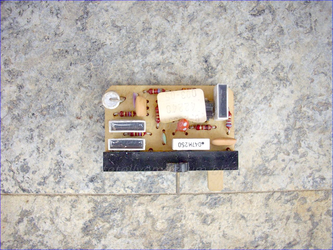


BILD-ZF-BAUSTEIN 29301-002
FARB BAUSTEIN 29301-024.01 TDA2510 TDA2521
VIDEO BST 29301-005.01
DIFFERENZ BAUSTEIN 29301.006.01
HORIZONTAL BST 29301-008.05
VERTIKAL BST 29301-009.05
REGEL BAUSTEIN 29301-035.03 (Horizontal thyristor circuit regulator Stabiliser with SN74121N)
NF-BAUSTEIN 29301-004.04
ABSTIMM BAUSTEIN TELEPILOT 8 29301-056.32 TMS3727 TMS3894 SN29799N
REGEL BAUSTEIN 29301-035.03 (Horizontal thyristor circuit regulator Stabiliser with SN74121N) LINE DEFL. REGULATION UNIT WITH SN74LS221N
The ’221 and ’LS221 devices are dual
multivibrators with performance characteristics
virtually identical to those of the ’121 devices.
Each multivibrator features a negative-transitiontriggered
input and a positive-transition-triggered
input, either of which can be used as an inhibit
input.

Pulse triggering occurs at a particular voltage level and is not directly related to the transition time of the input
pulse. Schmitt-trigger input circuitry (TTL hysteresis) for B input allows jitter-free triggering from inputs with
transition at rates as slow as 1 V/s, providing the circuit with excellent noise immunity, typically of 1.2 V. A high
immunity to VCC noise, typically of 1.5 V, also is provided by internal latching circuitry.
Once fired, the outputs are independent of further transitions of the A and B inputs and are a function of the timing
components, or the output pulses can be terminated by the overriding clear. Input pulses can be of any duration
relative to the output pulse. Output pulse length can be varied from 35 ns to the maximum by choosing
appropriate timing components. With Rext = 2 kΩ and Cext = 0, an output pulse typically of 30 ns is achieved
that can be used as a dc-triggered reset signal.
Output rise and fall times are TTL compatible and independentof pulse length. Typical triggering and clearing sequences are shown as a part of the switching characteristics
waveforms.
Pulse-width stability is achieved through internal compensation and is virtually independent of VCC and
temperature. In most applications, pulse stability is limited only by the accuracy of external timing components.
Jitter-free operation is maintained over the full temperature and VCC ranges for more than six decades of timing
capacitance (10 pF to 10 µF) and more than one decade of timing resistance (2 kΩ to 30 kΩ for the SN54221,
2 kΩ to 40 kΩ for the SN74221, 2 kΩ to 70 kΩ for the SN54LS221, and 2 kΩ to 100 kΩ for the SN74LS221).
Throughout these ranges, pulse width is defined by the relationship: tw(out) = CextRext In2 ≈ 0.7 CextRext. In
circuits where pulse cutoff is not critical, timing capacitance up to 1000 µF and timing resistance as low as 1.4 kΩ
can be used. Also, the range of jitter-free output pulse widths is extended if VCC is held to 5 V and free-air
temperature is 25°C. Duty cycles as high as 90% are achieved when using maximum recommended RT. Higher
duty cycles are available if a certain amount of pulse-width jitter is allowed.
The variance in output pulse width from device to device typically is less than ±0.5% for given external timing
components. An example of this distribution for the ’221 is shown in Figure 3. Variations in output pulse width
versus supply voltage and temperature for the ’221 are shown in Figures 4 and 5, respectively.
Pin assignments for these devices are identical to those of the SN54123/SN74123 or SN54LS123/SN74LS123
so that the ’221 or ’LS221 devices can be substituted for those products in systems not using the retrigger by
merely changing the value of Rext and/or Cext; however, the polarity of the capacitor must be changed.
FUNCTION TABLE
(each monostable multivibrator)
INPUTS OUTPUTS
CLR A B Q Q
L X X L H
X H X L H
X X L L H
H L ↑ † †
H ↓ H † †
↑‡ L H † †
† Pulsed-output patterns are tested during
AC switching at 25°C with Rext = 2 kΩ, and
Cext = 80 pF.
‡ This condition is true only if the output of
the latch formed by the two NAND gates
has been conditioned to the logic 1 state
prior to CLR going high. This latch is
conditioned by taking either A high or
B low while CLR is inactive (high).
absolute maximum ratings over operating free-air temperature range (unless otherwise noted)†
Supply voltage range, VCC 7 V . . . . . . . . . . . . . . . . . . . . . . . . . . . . . . . . . . . . . . . . . . . . . . . . . . . . . . . . . . . . . . . . . . .
Input voltage range, VI (see Note 1): ’LS221 7 V . . . . . . . . . . . . . . . . . . . . . . . . . . . . . . . . . . . . . . . . . . . . . . . . . . .
’221 5.5 V . . . . . . . . . . . . . . . . . . . . . . . . . . . . . . . . . . . . . . . . . . . . . . . . . . . .
Package thermal impedance, θJA (see Note 2): D package 73°C/W . . . . . . . . . . . . . . . . . . . . . . . . . . . . . . . . . . .
DB package 82°C/W . . . . . . . . . . . . . . . . . . . . . . . . . . . . . . . . .
N package 67°C/W . . . . . . . . . . . . . . . . . . . . . . . . . . . . . . . . . . .
NS package 64°C/W . . . . . . . . . . . . . . . . . . . . . . . . . . . . . . . . .
Storage temperature range, Tstg −65°C to 150°C.
TDA2591 SYNCHRO AND HORIZONTAL DEFLECTION CONTROL FOR COLOR TV SET
DESCRIPTION
The TDA2591 is a circuit intended for the horizontal
deflection of color TVsets, supplied with transistors
or SCR’S.
The TDA2591 and TDA2593 are integrated line
oscillator ‘_circuits for colour television receivers using
thyristor or transistor line deflection output stages.
The _circuits incorporate a line oscillator ‘which is
based on the threshold switching principle, a line de-
flection output stage capable of direct drive of thyristor
deflection circuits, phase comparison between the
oscillator voltage and both the sync pulse and line
flyback pulse. Also included on the chip is a switch for
changing the filter characteristic and the gate circuit
when used for VCR.
The TDA2593 generates a sandcastle pulse (at pin
7) suitable for use with the TDA.2532.
.LINE OSCILLATOR(two levels switching)
.PHASE COMPARISON BETWEEN SYNCHRO-
PULSE AND OSCILLATOR VOLTAGE Ø 1, ENABLED BY AN INTERNAL PULSE,
(better parasitic immunity)
PHASE COMPARISON BETWEEN THE FLYBACK
PULSES AND THE OSCILLATOR VOLTAGE Ø2
.COINCIDENCE DETECTOR PROVIDING A LARGE HOLD-IN-RANGE.
.FILTER CHARACTERISTICS AND GATE SWITCHING FOR VIDEO RECORDER APPLICATION.
.NOISE GATED SYNCHRO SEPARATOR
.FRAME PULSE SEPARATOR .BLANKING AND SAND CASTLE OUTPUT PULSES
.HORIZONTAL POWER STAGE PHASE LAGGING CIRCUIT
.SWITCHING OF CONTROL OUTPUT PULSE WIDTH
.SEPARATED SUPPLY VOLTAGE OUTPUT STAGE ALLOWING DIRECT DRIVE OF SCR’S CIRCUIT
.SECURITY CIRCUIT MAKES THE OUTPUT PULSE SUPPRESSED WHEN LOW SUPPLY
VOLTAGE.
TDA1170 vertical deflection FRAME DEFLECTION INTEGRATED CIRCUITGENERAL DESCRIPTION f The TDA1170 and TDA1270 are monolithic integrated
circuits designed for use in TV vertical deflection systems. They are manufactured using
the Fairchild Planar* process.
Both devices are supplied in the 12-pin plastic power package with the heat sink fins bent
for insertion into the printed circuit board.
The TDA1170 is designed primarily for large and small screen black and white TV
receivers and industrial TV monitors. The TDA1270 is designed primarily for driving
complementary vertical deflection output stages in color TV receivers and industrial
monitors.
APPLICATION INFORMATION (TDA1170)
The vertical oscillator is directly synchronized by the sync pulses (positive or negative); therefore its free
running frequency must be lower than the sync frequency. The use of current feedback causes the yoke
current to be independent of yoke resistance variations due to thermal effects, Therefore no thermistor is
required in series with the yoke. The flyback generator applies a voltage, about twice the supply voltage, to
the yoke. This produces a short flyback time together with a high useful power to dissipated power
ratio.
TDA2521 synchronous demodulator for PAL
GENERAL DESCRIPTION
The TDA2521 is a monolithic integrated circuit designed as a synchronous demodulator for PAL color television receivers. It includes an 8.8 MHz oscillator and divider, to generate two 4.4 MHz reference signals, and provides color difference output.

The TDA2521 is intended to interface directly with the TDA251O with a minimum of external components and is constructed on a single silicon chip using the Fairchild Planar
epitaxial process.
ABSOLUTE MAXIMUM RATINGS
Supply Voltage 14 V
Internal Power Dissipation 600 mW ORDER INFQRMATIQN
Operating Temperature Range —2O°C to +6O°C TYPE PART NO.
Storage Temperature Range —55°C to +125°C 2521 TDA2521
Pin Temperature iSo|dering 10 si 260°C
Planar is a patented Fairchild process
TDA2510 CHROMINANCE COMBINATION
GENERAL DESCRIPTION —

The TDA2510 is a monolithic integrated circuit designed for the function of a color television receiver. It Is designed to Interface directly with the TDA2521, using a minimum number of external components.
TDA251O is constructed on a single silicon chip using the Fairchild Planar‘ epitaxial process.
ABSOLUTE MAXIMUM RATINGS
supply Voltage 15 V
Collector voltage of chroma output transistor (pin 7) 20 V
(PD I 100 mW max)
Collector current of chroma output transistor (pin 7) 20 mA
Collector current of color killer output transistor (pin 11) 10 mA
Power dissipation 500 mW
Operating temperature range —25°C 10 +6O°
Storage temperature range *55°C to +12!-3°C.
Thyristors Used:
BstCC0146 7BR3 (Return / Ruecklauf)
BstCC0143 8JH21 (Trace / Hinlauf)
RCA 17127 (Regel Thyristor - Regulation Thyristor)
INTEGRAL THYRISTOR-RECTIFIER DEVICEA semiconductor switching device comprising a silicon controlled rectifier (SCR) and a diode rectifier integrally connected in parallel with the SCR in a single semiconductor body. The device is of the NPNP or PNPN type, having gate, cathode, and anode electrodes. A portion of each intermediate N and P region makes ohmic contact to the respective anode or cathode electrode of the SCR. In addition, each intermediate region includes a highly conductive edge portion. These portions are spaced from the adjacent external regions by relatively low conductive portions, and limit the conduction of the diode rectifier to the periphery of the device. A profile of gold recombination centers further electrically isolates the central SCR portion from the peripheral diode portion.
That class of thyristors known as controlled rectifiers are semiconductor switches having four semiconducting regions of alternate conductivity and which employ anode, cathode, and gate electrodes. These devices are usually fabricated from silicon. In its normal state, the silicon controlled rectifier (SCR) is non-conductive until an appropriate voltage or current pulse is applied to the gate electrode, at which point current flows from the anode to the cathode and delivers power to a load circuit. If the SCR is reverse biased, it is non-conductive, and cannot be turned on by a gating signal. Once conduction starts, the gate loses control and current flows from the anode to the cathode until it drops below a certain value (called the holding current), at which point the SCR turns off and the gate electrode regains control. The SCR is thus a solid state device capable of performing the circuit function of a thyratron tube in many electronic applications. In some of these applications, such as in automobile ignition systems and horizontal deflection circuits in television receivers, it is necessary to connect a separate rectifier diode in parallel with the SCR. See, for example, W. Dietz, U. S. Pat. Nos. 3,452,244 and 3,449,623. In these applications, the anode of the rectifier diode is connected to the cathode of the SCR, and the cathode of the rectifier is connected to the SCR anode. Thus, the rectifier diode will be forward biased and current will flow through it when the SCR is reverse biased; i.e., when the SCR cathode is positive with respect to its anode. For reasons of economy and ease of handling, it would be preferable if the circuit function of the SCR and the associated diode rectifier could be combined in a single device, so that instead of requiring two devices and five electrical connections, one device and three electrical connections are all that would be necessary. In fact, because of the semiconductor profile employed, many SCR's of the shorted emitter variety inherently function as a diode rectifier when reverse biased. However, the diode rectifier function of such devices is not isolated from the controlled rectifier portion, thus preventing a rapid transition from one function to the other. Therefore, it would be desirable to physically and electrically isolate the diode rectifier portion from that portion of the device which functions as an SCR.GRUNDIG SUPER COLOR 4232 CHASSIS 29301-374.21(03) orizontal deflection circuit with thyristors.(ZEILEN ABLENKUNG MIT THYRISTOREN SCHALTUNG)


Description:
1. A horizontal deflection circuit for generating the deflection current in the deflection coil of a television picture tube wherein a first switch controls the horizontal sweep, and wherein a second switch in a so-called commutation circuit with a commutating inductor and a commutating capacitor opens the first switch and, in addition, controls the energy transfer from a dc voltage source to an input inductor, characterized in that the input inductor (Le) and the commutating inductor (Lk) are combined in a unit designed as a transformer (U) which is proportioned so that the open-circuit inductance of the transformer is essentially equal to the value of the input inductor (Le), while the short-circuit inductance of the transformer (U) is essentially equal to the value of the commutating inductor (Lk), and that the second switch (S2) is connected in series with
the dc voltage source (UB) and a first winding (U1) of the transformer (U). 2. A horizontal deflection circuit according to claim 1, characterized in that the transformer (U) operates as an isolation transformer between the supply (UB) and the subcircuits connected to a second winding. 3. A horizontal deflection circuit according to claim 1, characterized in that the second switch (S2) is connected between ground and that terminal of the first winding (U1) of the transformer (U) not connected to the supply potential (+UB). 4. A horizontal deflection circuit according to claim 1, characterized in that a capacitor (CE) is connected across the series combination of the first winding (U1) of the transformer and the second switch (S2). 5. A horizontal deflection circuit according to claim 1, characterized in that the second winding (U2) of the transformer (U) is connected in series with a first switch (S1), the commutating capacitor (Ck), and a third, bipolar switch (S3) controllable as a function of the value of a controlled variable developed in the deflection circuit. 6. A horizontal deflection circuit according to claim 5, characterized in that the third switch (S3) is connected between ground and the second winding (U2) of the transformer. 7. A horizontal deflection circuit according to claim 2, characterized in that the isolation transformer carries a third winding via which power is supplied to the audio output stage of the television set. 8. A horizontal deflection circuit according to claims 2, characterized in that the voltage serving to control the first switch (S1) is derived from a third winding of the transformer.
Description:
The present invention relates to a horizontal deflection circuit for generating the deflection current in the deflection coil of a television picture tube wherein a first switch controls the horizontal sweep, and wherein a second switch in a so-called commutation circuit with a commutating inductor and a commutating capacitor opens the first switch and, in addition, controls the energy transfer from a dc voltage source to an input inductor.German Auslegeschrift (DT-AS) No. 1,537,308 discloses a horizontal deflection circuit in which, for generating a periodic sawtooth current within the respective deflection coil of the picture tube, in a first branch circuit, the deflection coil is connected to a sufficiently large capacitor serving as a current source via a first controlled, bilaterally conductive switch which is formed by a controlled rectifier and a diode connected in inverse parallel. The control electrode of the rectifier is connected to a drive pulse source which renders the switch conductive during part of the sawtooth trace period. In that arrangement, the sawtooth retrace, i.e. the current reversal, also referred to as "commutation", is initiated by a second controlled switch.
The first controlled switch also forms part of a second branch circuit where it is connected in series with a second current source and a reactance capable of oscillating. When the first switch is closed, the reactance, consisting essentially of a coil and a capacitor, receives energy from the second current source during a fixed time interval. This energy which is taken from the second current source corresponds to the circuit losses caused during the previous deflection cycle.
As can be seen, such a circuit needs two different, separate inductive elements, it being known that inductive elements are expensive to manufacture and always have a certain volume determined by the electrical properties required.
The object of the invention is to reduce the amount of inductive elements required.
The invention is characterized in that the input inductor and the commutating inductor are combined in a unit designed as a transformer which is proportioned so that the open-circuit inductance of the transformer is essentially equal to the value of the input inductor, while the short-circuit inductance of the transformer is essentially equal to the value of the commutating inductor, and that the second switch is connected in series with the dc voltage source and a first winding of the transformer.
This solu
 tion has an added advantage in that, in mass production, both the open-circuit and the short-circuit inductance are reproducible with reliability.
According to another feature of the invention, the electrical isolation between the windings of the transformer is such that the transformer operates as an isolation transformer between the supply and the subcircuits connected to a second winding or to additional windings of the transformer. In this manner, the transformer additionally provides reliable mains isolation.
According to a further feature of the invention, the second switch is connected between ground and that terminal of the first winding of the transformer not connected to the supply potential. This simplifies the control of the switch.
According to a further feature of the invention, to regulate the energy supply, the second winding of the transformer is connected in series with the first switch, the commutating capacitor, and a third, bipolar switch controllable as a function of the value of a controlled variable developed in the deflection circuit.
The advantage gained by this measure lies in the fact that the control takes place on the side separated from the mains, so no separate isolation device is required for the gating of the third switch. Further details and advantages will be apparent from the following description of the accompanying drawings and from the claims. In the drawings,
FIG. 1 is a basic circuit diagram of the arrangement disclosed in German Auslegeschrift (DT-AS) No. 1,537,308;
FIG. 2 shows a first embodiment of the horizontal deflection circuit according to the invention, and
FIG. 3 shows a development of the horizontal deflection circuit according to the invention.
FIG. 1 shows the essential circuit elements of the horizontal deflection circuit known from the German Auslegeschrift (DT-AS) No. 1,537,308 referred to by way of introduction.
Connected in series with a dc voltage source UB is an input inductor Le and a bipolar, controlled switch S2. In the following, this switch will be referred to as the "second switch"; it is usually called the "commutating switch" to indicate its function.
In known circuits, the second switch S2 consists of a controlled rectifier and a diode connected in inverse parallel.
The second switch S2 also forms part of a second circuit which contains, in addition, a commutating inductor Lk, a commutating capacitor Ck, and a first switch S1. The first switch S1, controlling the horizontal sweep, is c
onstructed in the same manner as the above-described second switch S2, consisting of a controlled rectifier and a diode in inverse parallel. Connected in parallel with this first switch is a deflection-coil arrangement AS with a capacitor CA as well as a high voltage generating arrangement (not shown). In FIGS. 1, 2, and 3, this arrangement is only indicated by an arrow and by the reference characters Hsp. The operation of this known horizontal deflection circuit need not be explained here in detail since it is described not only in the German Auslegeschrift referred to by way of introduction, but also in many other publications.FIGS. 2 and 3 show the horizontal deflection circuit modified in accordance with the present invention. Like circuit elements are designated by the same reference characters as in FIG. 1.
FIG. 2 shows the basic principle of the invention. The two inductors Le and Lk of FIG. 1 have been replaced by a transformer U. To be able to serve as a substitute for the two inductors Le and Lk, the transformer must be proportioned in a special manner. Regardless of the turns ratio, the open-circuit inductance of the transformer is chosen to be essentially equal to the value of the input inductor Le, and the short-circuit inductance of the transformer is essentially equal to the value of the commutating inductor Lk.
To permit the second switch S2 to be utilized for the connection of the dc voltage source UB, it is included in the circuit of that winding U1 of the transformer connected to the dc voltage UB.
In principle, it is of no consequence for the operation of the switch S2 whether it is inserted on that side of the winding U1 connected to the positive operating potential +UB or on the side connected to ground. In practice, however, the solution shown in FIGS. 2 and 3 will be chosen since the gating of the controlled rectifier is less problematic in this case.
In compliance with pertinent safety regulations, the transformer U may be designed as an isolation transformer and can thus provide mains separation, which is necessary for various reasons. It is known from German Offenlegungschrift (DT-OS) No. 2,233,249 to provide dc isolation by designing the commutating inductor as a transformer, but this measure is not suited to attaining the object of the present invention.
If the energy to be taken from the dc voltage source is to be controlled as a function of the energy needed in the horizontal deflection circuit and in following subcircuits, the embodiment of the horizontal deflection circuit of FIG. 3 may be used.
The circuit including the winding U2 of the transformer U contains a third controlled switch S3, which, too, is inserted on the grounded side of the winding U2 for the reasons mentioned above. This third switch S3, just as the second switch S2, is operated at the frequency of a horizontal oscillator HO, but a control circuit RS whose input l is fed with a controlled variable is inserted between the oscillator and the switch S3. Depending on this controlled variable, the controlled rectifier of the third switch S3 can be caused to turn on earlier. A suitable controlled variable containing information on the energy consumption is, for example, the flyback pulse capable of being taken from the high voltage generating circuit (not shown). Details of the operation of this kind of energy control are described in applicant's German Offenlegungsschrift (DT-OS) No. b 2,253,386 and do not form part of the present invention.
With mains isolation, the additional, third switch S3 shown here has the advantage of being on the side isolated from the mains and eliminates the need for an isolation device in the control lead of the controlled rectifier.
As an isolation transformer, the transformer U may also carry additional windings U3 and U4 if power is to be supplied to the audio output stage, for example; in addition, the first switch S1 may be gated via such an additional winding.
The points marked at the windings U1 and U2 indicate the phase relationship between the respective voltages. Connected in parallel with the winding U1 and the second switch S2 is a capacitor CE which completes the circuit for the horizontal-frequency alternating current; this serves in particular to bypass the dc voltage source or the electrolytic capacitors contained therein.
If required, a well-known tuning coil may be inserted, e.g. in series with the second winding U2, without changing the basic operation of the horizontal deflection circuit according to the invention.
Electron beam deflection circuit including thyristors Further Discussion and deepening of knowledge, Thyristor horizontal output circuits:GRUNDIG SUPER COLOR 4232 CHASSIS 29301-374.21(03)
1. An electron beam deflection circuit for a cathode ray tube with electromagnetic deflection by means of a sawtooth current waveform having a trace portion and a retrace portion, said circuit comprising: a deflection winding; a first source of electrical energy formed by a first capacitor; first controllable switching means comprising a parallel combination of a first thyristor and a first diode connected together to conduct in opposite directions, for connecting said winding to said first source during said trace portion, while said first switching means is turned on; a second source of electrical energy including a first inductive energy storage means coupled to a voltage supply; reacti
ve circuit means including a combination of inductive and capacitive reactances for storing the energy supplied by said second source; second controllable switching means, substantially similar to said first one, for completing a circuit including said reactive circuit means and said first switching means, when turned on before the end of said trace portion, so as to pass through said first switching means an oscillatory current in opposite direction to that which passes through said first thyristor from said first source and to turn said first thyristor off after these two currents cancel out, the oscillatory current flowing thereafter through said first diode for an interval termed the circuit turn-off time, which has to be greater than the turn-off time of said first thyristor; wherein the improvement comprises: means for drawing, during at least a part of said trace portion, a substantial amount of additional current through said first switching means, in the direction of conduction of said first diode, whereby to perceptibly shift the waveform of the current flowing through said first switching means towards the negative values by an amount equal to that of said substantial additional current and to lengthen, in proportion thereto, said circuit turn-off time, without altering the values of the reactances in the reactive circuit which intervene in the determination of both the circuit turn-off and retrace portion time intervals.
2. A deflection circuit as claimed in claim 1, wherein said amount of additional current is greater than or equal to 5 per cent of the peak-to-peak value of the current flowing through the deflection winding.
3. A deflection circuit as claimed in claim 1, wherein said means for drawing a substantial amount of additional current through said first switching means comprises a resistor connected in parallel to said first capacitor.
4. A deflection circuit as claimed in claim 1, wherein said means for drawing an additional current is formed by connecting said first and second energy sources in series so that the current charging said reactive circuit means forms the said additional current.
5. A deflection circuit as claimed in claim 1, further including a series combination of an autotransformer winding and a second high-value capacitor, said combination being connected in parallel to said first switching means, wherein said autotransformer comprises an intermediate tap located between its terminals respectively connected to said first switching means and to said second capacitor, said tap delivering, during said trace portion, a suitable DC supply voltage lower than the voltage across said second capacitor; and wherein said means for drawing a substantial amount of additional current comprises a load to be fed by said supply voltage and having one terminal connected to ground; and further controllable switching means controlled to conduct during at least part of said trace portion and to remain cut off during said retrace portion, said further switching means being connected between said tap and the other terminal of said load.
Description:
The present invention relates to electron beam deflection circuits including thyristors, such as silicon controlled rectifiers and relates, in particular, to horizontal deflection circuits for television receivers.
 The present invention constitutes an improvement in the circuit described in U.S. Pat. No. 3,449,623 filed on Sept. 6, 1966, this circuit being described in greater detail below with reference to FIGS. 1 and 2 of the accompanying drawings. A deflection circuit of this type comprises a first thyristor switch which allows the conenction of the horizontal deflection winding to a constant voltage source during the time interval used for the transmisstion of the picture signal and for applying this signal to the grid of the cathode ray tube (this interval will be termed the "trace portion" of the scan), and a second thyristor switch which provides the forced commutation of the first one by applying to it a reverse current of equal amplitude to that which passes through it from the said voltage source and thus to initiate the retrace during the horizontal blanking interval.
A undirectional reverse blocking triode type thyristor or silicon controlled rectifier (SCR), such as that used in the aformentioned circuit, requires a certain turn-off time between the instant at which the anode current ceases and the instant at which a positive bias may be applied to it without turning it on, due to the fact that there is still a high concentration of free carriers in the vicinity of the middle junction, this concentration being reduced by a process of recombination independently from the reverse polarity applied to the thyristor. This turn-off time of the thyristor is a function of a number of parameters such as the junction temperature, the DC current level, the decay time of the direct current, the peak level of the reverse current applied, the amplitude of the reverse anode to cathode voltage, the external impedance of the gate electrode, and so on, certain of these varying considerably from one thyristor to another.
In horizontal deflection circuits for television receivers, the flyback or retrace time is limited to approximately 20 percent of the horizontal scan period, the retrace time being in the case of the CCIR standard of 625 lines, approximately 12 microseconds and, in the case of the French standard of 819 lines, approximately 9 microseconds. During this relatively short interval, the thyristor has to be rendered non-conducting and the electron beam has to be returned to the origin of the scan. The first thyristor is blocked by means of a series resonant LC circuit which is subject to a certain number of restrictions (limitations as to the component values employed) due to the fact that, inter alia, it simultaneously determines the turn-off time of the circuit which blocks the thyristor and it forms part of the series resonant circuit which is to carry out the retrace. To obtain proper operation of the deflection circuit of the aforementioned Patent, especially when used for the French standard of 819 lines per image, the values of the components used have to subject to very close tolerances (approximately 2%), which results in high costs.
 The improved deflection circuit, object of the present invention, allows the lengthening of the turn-off time of the circuit for turning the scan thyristor off, without altering the values of the LC circuit, which are determined by other criteria, and without impairing the operation of the circuit.
According to the invention, there is provided an electron beam deflection circuit for a cathode ray tube with electromagentic deflection by means of a sawtooth current waveform having a trace portion and a retrace portion, said circuit comprising: a deflection winding; a first source of electrical energy formed by a first capacitor; first controllable switching means comprising a parallel combination of a first thyristor and a first diode, connected together to conduct in opposite directions, for connecting said winding to said first source during said trace portion when said first switching means is turned on; a second source of electrical energy including a first inductive energy storage means coupled to a voltage supply; reactive circuit means including a combination of inductive and capacitive reactances for storing the energy supplied by the said second source; a second controllable switching means, substantially identical with the first one, for completing a circuit including said reactive circuit means and said first switching means, when turned on, so as to pass through said first thyristor an oscillatory current in the opposite direction to that which passes through it from said first source and to turn it off after these two currents can cel out, the oscillatory current then flowing through said first diode for an interval termed the circuit turn-off time which has to be greater than the turn-off time of said first thyristor; and means for drawing duing at least a part of said trace portion a substantial amount of additional current from said first switching means in the direction of conduction of said first diode, whereby said circuit turn-off time is lengthened in proportion to the amount of said additional current, without altering the values of the reactances in the reactive circuit by shifting the waveform of the current flowing through said first switching means towards the negative by an amount equal to that of said additional current.
A further object of the invention consists in using the supplementary current in the recovery diode of the first switching means to produce a DC voltage which may be used as a power supply for the vertical deflection circuit of the television receiver, for example.
The invention will be better understood and other features and advantages thereof will become apparent from the following description and the accompanying drawings, given by way of example, and in which:
FIG. 1 is a schematic circuit diagram partially in bloc diagram form of a prior art deflection circuit according to the aforementioned Patent;
FIG. 2 shows waveforms of currents and voltages generated at various points in the circuit of FIG. 1;
FIG. 3 is a schematic diagram of a deflection circuit according to the invention which allows the principle of the improvement to be explained;
FIG. 4 is a diagram of the waveforms of the current through the first switching means 4, 5 of the circuit of FIG. 3;
FIG. 5 is a circuit diagram of another embodiment of the circuit according to the invention;
FIG. 6 is a schematic representation of the preferred embodiment of the circuit according to the invention; and
FIG. 7 shows voltage waveforms at various points of the high voltage autotransformer 21 of FIG. 6.
In all these Figures the same reference numerals refer to the same components.
 FIG. 1 shows the horizontal deflection circuit described and claimed in the U.S. Pat. No. 3,449,623 mentioned above, which comprises a first source of electrical energy in the shape of a first capacitor 2 having a high capacitance C 2 for supplying a substantially constant voltage Uc 2 across its terminals. A first terminal of the first capacitor 2 is connected to ground, whilst its second terminal which supplies a positive voltage is connected to one of the terminals of a horizontal deflection winding shown as a first inductance 1. A first switching means 3, consisting of a first reverse blocking triode thyristor 4 (SCR) and a first recovery diode 5 in parallel, the two being interconnected to conduct current in opposite directions, is connected in parallel with the series combination formed by the deflection winding 1 and the first capacitor 2. The assembly of components 1, 2, 4 and 5 forms the final stage of the horizontal deflection circuit in a television receiver using electromagnetic delfection.
The deflection circuit also includes a drive stage for this final stage which here controls the turning off of the first thyristor 4 to produce the retrace or fly-back portion of the scan during the line-blanking intervals i.e. while the picture signal is not transmitted. This driver stage comprises a second voltage source in the shape of a DC power supply 6 which delivers a constant high voltage E. The negative terminal of the power supply 6 is connected to ground and its positive terminal to one of the terminals of a second inductance 7 of relatively high value, which draws a substantially lineraly varying current from the power supply 6 to avoid its overloading. The other terminal of the second inductance 7 is connected, on the one hand, to the junction of the deflection winding 1 and the first switching means 3 by means of a second inductance 8 and a second capacitor 9 in series and, on the other hand, to one of the terminals of a second controllable bi-directionally conducting switching means 10, similar to the first one 3, including a parallel combination of a second thyristor 11 and a second recovery diode 12 also arranged to conduct in opposite directions.
The respective values of the third inductance 8 (L 8 ) and of the second capacitor 9 (C 9 ) are principally selected so that, on the one hand, one half-cycle of oscillation of the first series resonant circuit L 8 - C 9 , (i.e. π √ L 8 . C 9 ) is longer than the turn-off time of the first thyristor 4, but still is as short as possible since this time interval determines the speed of the commutation of the thyristor 4, and, on the other hand, one half-cycle of oscillation of another series resonant circuit formed by L 1 , L 8 and C 9 , i.e. π √ (L 1 + L 8 ) . C 9 , is substantially equal to the required retrace time interval (i.e. shorter than the horizontal blanking interval).
The gate (control electrode) of the second thyristor 11 is coupled to the output of the horizontal oscillator 13 of the television receiver by means of a first pulse transformer 14 and a first pulse shaping circuit 15 so that it is fed short triggering pulses which are to turn it on.
The gate of the first thyristor 4 fed with signals of a substantially rectangular waveform which are negative during the horizontal blanking intervals, is coupled to a winding 16 by means of a second pulse shaping circuit 17, the winding 16 being magnetically coupled to the second inductance 7 to make up the secondary winding of a transformer of which the inductance 7 forms the primary winding. It will be noted here that it is also possible to couple the secondary winding 16 magnetically to a primary winding connected to a suitable output (not shown) of the horizontal oscillator 13.
The operation of a circuit of this type will be explained below with reference to FIG. 2 which shows the waveforms at various points in the circuit of FIG. 1 during approximately one line period.
FIG. 2 is not to scale since one line period (t 7 - t 0 ) is equal to 64 microseconds in the case of 625 lines and 49 microseconds in the case of 819 lines, while the durations of the respective horizontal blanking intervals are approximately 12 and 9.5 microseconds.
Waveform A shows the form of the current i L1 passing through deflection winding 1, this current having a sawtooth waveform substantially linear from t 0 to t 3 and from t 5 to t 7 , and crossing zero at time instants t 0 and t 7 , and reaching values of + I 1m and - I 1m , at time instants t 3 and t 5 respectively, these being its maximum positive and negative amplitudes.
During the second half of the trace portion of the horizontal deflection cycle, that is to say from t 0 to t 3 , the thyristor 4 of the first switching means 3 is conductive and makes the high value capacitor 2 discharge through the deflector winding 1, which has a high inductance, so that current i L1 increases linearly.
A few microseconds (5 to 8 μ s) before the end of the trace portion, i.e. at time instant t 1 , the trigger of the second thyristor 11 receives a short voltage pulse V G11 which causes it to turn on as its anode is at this instant at a positive potential with respect to ground, which is due to the charging of the second capacitor 9 through inductances 7 and 8 by the voltage E from the power supply 6.
 When thyristor 11 is made conductive at time t 1 , on the one hand, inductance 7 is connected between ground and the voltage source 6 and a linearly increasing current flows through it and, on the other hand, the reactive circuit 8, 9 forms a loop through the second and first switching means 10 and 3, thus forming a resonant circuit which draws an oscillatory current i 8 ,9 of frequency ##EQU1##
This oscillatory current i 8 ,9 will pass through the first switching means 3, i.e. thyristor 4 and diode 5, in the opposite direction to that of current i L1 . Since the frequency f 1 is high, current i 8 ,9 will increase more rapidly than i L1 and will reach the same level at time t 2 , that is to say i 8 ,9 (t 2 ) = -i L1 (t 2 ) and these currents will cancel out in the thyristor 4 in accordance with the well known principle of forced commutation. After time instant t 2 , current i 8 ,9 continues to increase more rapidly than i L1 , but the difference between them (i 8 ,9 - i L1 ) passes the diode 5 (see wave form B) until it becomes zero at time instant t 3 which is the turn off time instant of the first switching means 3, at which the retrace begins.
The interval between the time instant t 2 and t 3 , i.e. (t 3 -t 2 ), during which diode 5 is conductive and the thyristor is reverse biased will be termed in what follows the circuit turn-off time and it should be greater than the turn-off time of the thyristor 4 itself since the latter will subsequently become foward biased (i.e. from t 3 to t 5 ) by the retrace or flyback pulse (see waveform E) which should not trigger it.
At time instant t 3 , the switching means 3 is opened (i 4 and i 5 are both zero -- see waveforms B and C) and the reactive circuit 8, 9 forms a loop through capacitor 2 and the deflection coil 1 and thus a series resonant circuit including (L 1 + L 8 ) and C 9 , C 2 being of high value and representing a short circuit for the flyback frequency ##EQU2## thus obtained.
The retrace which stated at time t 3 takes place during one half-cycle of the resonant circuit formed by reactances L 1 , L 8 and C 9 , i.e. during the interval between t 3 and t 5 . In the middle of this interval i.e. at time instant t 4 , both i L1 (waveform A) and i 8 ,9 (waveform D) pass through zero and change their sign, whereas the voltage at the terminals of the first switching means 3 (V 3 , waveform E) passes through a maximum. Thus, from t 4 onwards, thyristor 11 will be reverse biased and diode 12 will conduct the current from the resonant circuit 1, 8 and 9 in order to turn the second thyristor 11 off.
At time instant t 5 , when current i L1 has reached - I 1m and when voltage v 3 falls to zero, diode 5 of the first switching means 3 becomes conductive and the trace portion of scan begins.
Current i 8 ,9 nevertheless continues to flow in the resonant circuit 8, 9 through diodes 5 and 12, which causes a break to appear in waveform D at t 5 , and a negative peak to appear in waveform D and a positive one in waveform B in the interval between t 5 and t 6 , these being principally due to the distributed capacities of coil 1 or to an eventual capacitor (not shown) connected in parallel to the first switching means 3.
At time instant t 6 , diode 12 of the second switching means 10 ceases to conduct after having allowed thyristor 11 time to become turned off completely.
The level of current i 8 ,9 at time instant t 5 (i.e. I c ) as well as the negative peak I D12 in i 8 ,9 and the positive peak I D5 in i 5 depend on the values of L 8 and C 9 in the same way as does the turn-off time of the circuit (t 3 - t 2 ). If, for example, L 8 and C 9 , are increased I D5 increases towards zero and this could cause diode 5 to be cut off in an undesirable fashion. I c also increases towards zero, which is liable to cause diode 12 to be blocked and thyristor 11 to trigger prematurely.
From the foregoing it can be clearly seen that the choice of values for L 8 and C 9 is subject to four limitations which prevent the values from being increased to lengthen the turn-off time of the driver circuit of first switching thyristor 4 so as to forestall its spurious triggering.
Waveform F shows the voltage v G4 obtained at the gate of thyristor 4 from the secondary winding 16 coupled to the inductor 7. This voltage is positive from t 0 to t 1 and from t 6 to t 7 and is negative between t 2 and t 6 i.e. while the second switching means 10 is conducting.
The present invention makes the lengthening of the turn-off time of thyristor 4 possible without altering the parameters of the circuit such as inductance 8 and capacitor 9.
 In the circuit shown in FIG. 3, which illustrates the principle of the present invention, means are added to the circuit in FIG. 1 which enable the turn-off time to be lengthened by connecting a load to diode 5 so as to increase the current which flows through it during the time that it is conductive. These means are here formed by a resistor 18 connected in parallel with a capacitor 20 (which replaces capacitor 2) which is of a higher capacitance so that, in practice, it holds its charge during at least one half of the line period. FIG. 4, which shows the waveform of the current in the first switching means 3 for a circuit as shown in FIG. 3, makes it possible to explain how this lenthening of the turn-off time is achieved.
In FIG. 4, the broken lines show the waveform of the current in the first switch device 3 in the circuit of FIG. 1, this waveform being produced by adding waveforms B and C of FIG. 2. The current i 4 above the axis flows through thyristor 4 and current i 5 below the axis flows through diode 5. When the capacitance C 20 of the capacitor in series with the deflector coil is increased to some tens of microfarads (C 2 having been of the order of 1 μ F) and when there is connected in parallel with capacitor 20 a resistor 18 the value of which is calculated to draw a strong current I R18 from capacitor 20, that is to say a current at least equal to 0,1 I m (I m being of the order of some tens of amperes), current I R18 is added to that i 5 which flows through diode 5 without in any way altering the linearity of the trace portion nor the oscillatory commutation of thyristor 4 which is brought about by the resonant circuit L 8 , C 9 .
The fact of loading capacitor C 20 by means of a resistor 18 thus has the effect of permanently displacing the waveform of the current in the negative direction by I R18 . Thus, during the trace portion of the scan, the transfer of the current from the diode 5 to the thyristor 4 begins at time t 10 instead of t 0 , that is to say with a delay proportional to I R18 . The effect of the triggering pulse delivered by the horizontal oscillator (13 FIG. 1) to the second thyristor 11 at time instant t 1 , will be to start the commutation process of the first thyristor 4 when the current it draws is less by I R18 than that i 4 (t 1 ) which it would have been drawing had there been no resistor 18. Because of this, the turn-off time of the thyristor 4 proper, which as has been mentioned increases with the maximum current level passing throught it, is slightly reduced. Moreover, because the oscillatory current i 8 ,9 (FIG. 2) from circuit L 8 , C 9 which flows through thyristor 4 in the opposite direction is unchanged, it reaches a value equal to that of the current i L1 (FIG. 1) flowing in the coil 1 in a shorter time, that is to say at time t 12 . Diode 5 will thus take the oscillatory current i 8 ,9 (FIG. 2) over in advance with respect ro time instant t 2 and will conduct it until it reaches zero value at a time instant t 13 later than t 3 , the amounts of advance (t 2 - t 12 ) and delay (t 13 - t 3 ) being practically equal.
It can thus be seen in FIG. 4 that the circuit turn-off time T R of a circuit according to the invention and illustrated by FIG. 3 is distinctly longer than that T r of the circuit in FIG. 1. This increase in the turn-off time (T R - T r ) depends on the current I R18 and increases therewith.
It should be noted at this point that the current I R18 produces a voltage drop at the terminals of the resistor the only effect of which is to heat up the resistor since the level of this voltage (40 to 60 volts) does not necessarily have a suitable value to be used as a voltage supply for other circuits in an existing transistorised television receiver.
In accordance with one embodiment of the invention, illustrated in FIG. 5, an application is proposed for the additional current which is to be drawn through diode 5. In FIG. 5, the positive terminal of capacitor 20 is connected by a conductor 19 to the negative pole of the power supply 6 and the voltage at the terminals of capacitor 20 is thus added to that E from the source 6.
In the preferred embodiment of the present invention, which is shown in FIG. 6, it is possible to cause a supplementary current of a desired value to flow through the first diode 5 while obtaining a voltage which has a suitable value for use in another circuit in the television receiver.
If the voltage at the terminals of capacitor 20 in FIG. 3 is not a usable value, it is possible to connect in parallel with the series circuit comprising the deflector coil 1 and the capacitor 2 in FIG. 1, i.e. in parallel with the terminals of the first switching means 3, a series combination of an autotransformer 21 and a high value capacitor 22 (comparable with capacitor 20 in FIGS. 3 and 5). The autotransformer 21 has a tap 23 is suitably positioned between the terminal connected to capacitor 22 at the tap 24 connected to the first switching means 3. This autotransformer 21 may be formed by the one conventionally used for supplying a very high voltage to the cathode ray tube, as described for example in U.S. Pat. No. 3,452,244; such a transformer comprises a voltage step-up winding between taps 24 and 25, which latter is connected to a high voltage rectifier (not shown).
The waveform of the voltage at the various points in the autotransformer is shown in FIG. 7, in which waveform A shows the voltage at the terminals of capacitor 22, waveform B the voltage at tap 24 and waveform C the voltage at tap 23 of the autotransformer 21.
The voltage V c22 at the terminals of capacitor 22 varies slightly about a mean value V cm . It is increasing while diode 5 is conducting and decreasing during the conduction of the thyristor 4.
The voltage v 24 at tap 24 follows substantially the same curve as waveform E in FIG. 2, that is to say that during the retrace time interval from t 13 to t 5 to a positive pulse called the flyback pulse is produced and, during the time interval while the first switching means 3 is conducting, the voltage is zero. The mean valve of the voltage v 24 at tap 24 of the auto-transformer 21 is equal to the mean value V cm of the voltage at the terminals of capacitors 2 and 22.
Thus, there is obtained at tap 23 a waveform which is made up, during the retrace portion, of a positive pulse whose maximum amplitude is less than that of v 24 at tap 24 and, during the trace portion, of a substantially constant positive voltage, the level V of which is less than the mean value V cm of the voltage v c22 at the terminals of capacitor 22. By moving tap 23 towards terminals 24 the amplitude of the pulse during fly-back increases while voltage V falls and conversely by moving tap 23 towards capacitor 22 voltage V increases and the amplitude of the pulse drops.
In more exact terms, the voltage V at tap 23 is such that the means value of v 23 is equal to V cm . It has thus been shown that by choosing carefully the position of tape 23, a voltage V may be obtained during the trace portion of the scan, which may be of any value between V cm and zero.
This voltage V is thus obtained by periodically controlled rectification during the trace portion of the scan. For this purpose an electronic switch is used to periodically connect the tap 23 of trnasformer winding 21 to a load. This switch is made up of a power transistor 26 whose collector is connected to tap 23 and the emitter to a parallel combination formed by a high value filtering capacitor 27 and the load which it is desired to supply, which is represented by a resistor 28. The base of the transistor 26 receives a control voltage to block it during retrace and to unblock it during the whole or part of the trace period. A control voltage of this type may be obtained from a second winding 29 magnetically coupled to the inductance 7 of the deflection circuit and it may be transmitted to the base of transistor 26 by means of a coupling capacitor 30 and a resistor 31 connected between the base and the emitter of transistor 26.
It may easily be seen that the DC collector/emitter current in transistor 26 flows through the first diode 5 of the first switching means 3 via a resistor 28 and the part of the winding of auto-transformer 21 located between taps 23 and 24.
Experience has shown that a circuit as shown in FIG. 6 can supply 24 volts with a current of 2 amperes to the vertical deflection circuit of the same television set, the voltage at the terminals of capacitor 22 being from 50 to 60 volts.
It should be mentioned that, when the circuit which forms the load of the controlled rectifier 26, 27 does not draw enough current to sufficiently lengthen the circuit turn-off time T R , an additional resistor (not shown) may be connected between the emitter of transistor 26 and ground or in parallel to capacitor 22, which resistor will draw the additional current required.
 The present invention constitutes an improvement in the circuit described in U.S. Pat. No. 3,449,623 filed on Sept. 6, 1966, this circuit being described in greater detail below with reference to FIGS. 1 and 2 of the accompanying drawings. A deflection circuit of this type comprises a first thyristor switch which allows the conenction of the horizontal deflection winding to a constant voltage source during the time interval used for the transmisstion of the picture signal and for applying this signal to the grid of the cathode ray tube (this interval will be termed the "trace portion" of the scan), and a second thyristor switch which provides the forced commutation of the first one by applying to it a reverse current of equal amplitude to that which passes through it from the said voltage source and thus to initiate the retrace during the horizontal blanking interval.
A undirectional reverse blocking triode type thyristor or silicon controlled rectifier (SCR), such as that used in the aformentioned circuit, requires a certain turn-off time between the instant at which the anode current ceases and the instant at which a positive bias may be applied to it without turning it on, due to the fact that there is still a high concentration of free carriers in the vicinity of the middle junction, this concentration being reduced by a process of recombination independently from the reverse polarity applied to the thyristor. This turn-off time of the thyristor is a function of a number of parameters such as the junction temperature, the DC current level, the decay time of the direct current, the peak level of the reverse current applied, the amplitude of the reverse anode to cathode voltage, the external impedance of the gate electrode, and so on, certain of these varying considerably from one thyristor to another.
In horizontal deflection circuits for television receivers, the flyback or retrace time is limited to approximately 20 percent of the horizontal scan period, the retrace time being in the case of the CCIR standard of 625 lines, approximately 12 microseconds and, in the case of the French standard of 819 lines, approximately 9 microseconds. During this relatively short interval, the thyristor has to be rendered non-conducting and the electron beam has to be returned to the origin of the scan. The first thyristor is blocked by means of a series resonant LC circuit which is subject to a certain number of restrictions (limitations as to the component values employed) due to the fact that, inter alia, it simultaneously determines the turn-off time of the circuit which blocks the thyristor and it forms part of the series resonant circuit which is to carry out the retrace. To obtain proper operation of the deflection circuit of the aforementioned Patent, especially when used for the French standard of 819 lines per image, the values of the components used have to subject to very close tolerances (approximately 2%), which results in high costs.
According to the invention, there is provided an electron beam deflection circuit for a cathode ray tube with electromagentic deflection by means of a sawtooth current waveform having a trace portion and a retrace portion, said circuit comprising: a deflection winding; a first source of electrical energy formed by a first capacitor; first controllable switching means comprising a parallel combination of a first thyristor and a first diode, connected together to conduct in opposite directions, for connecting said winding to said first source during said trace portion when said first switching means is turned on; a second source of electrical energy including a first inductive energy storage means coupled to a voltage supply; reactive circuit means including a combination of inductive and capacitive reactances for storing the energy supplied by the said second source; a second controllable switching means, substantially identical with the first one, for completing a circuit including said reactive circuit means and said first switching means, when turned on, so as to pass through said first thyristor an oscillatory current in the opposite direction to that which passes through it from said first source and to turn it off after these two currents can
cel out, the oscillatory current then flowing through said first diode for an interval termed the circuit turn-off time which has to be greater than the turn-off time of said first thyristor; and means for drawing duing at least a part of said trace portion a substantial amount of additional current from said first switching means in the direction of conduction of said first diode, whereby said circuit turn-off time is lengthened in proportion to the amount of said additional current, without altering the values of the reactances in the reactive circuit by shifting the waveform of the current flowing through said first switching means towards the negative by an amount equal to that of said additional current.A further object of the invention consists in using the supplementary current in the recovery diode of the first switching means to produce a DC voltage which may be used as a power supply for the vertical deflection circuit of the television receiver, for example.
The invention will be better understood and other features and advantages thereof will become apparent from the following description and the accompanying drawings, given by way of example, and in which:
FIG. 1 is a schematic circuit diagram partially in bloc diagram form of a prior art deflection circuit according to the aforementioned Patent;
FIG. 2 shows waveforms of currents and voltages generated at various points in the circuit of FIG. 1;FIG. 3 is a schematic diagram of a deflection circuit according to the invention which allows the principle of the improvement to be explained;
FIG. 4 is a diagram of the waveforms of the current through the first switching means 4, 5 of the circuit of FIG. 3;
FIG. 5 is a circuit diagram of another embodiment of the circuit according to the invention;
FIG. 6 is a schematic representation of the preferred embodiment of the circuit according to the invention; and
FIG. 7 shows voltage waveforms at various points of the high voltage autotransformer 21 of FIG. 6.
In all these Figures the same reference numerals refer to the same components.
FIG. 1 shows the horizontal deflection circuit described and claimed in the U.S. Pat. No. 3,449,623 mentioned above, which comprises a first source of electrical energy in the shape of a first capacitor 2 having a high capacitance C 2 for supplying a substantially constant voltage Uc 2 across its terminals. A first terminal of the first capacitor 2 is connected to ground, whilst its second terminal which supplies a positive voltage is connected to one of the terminals of a horizontal deflection winding shown as a first inductance 1. A first switching means 3, consisting of a first reverse blocking triode thyristor 4 (SCR) and a first recovery diode 5 in parallel, the two being interconnected to conduct current in opposite directions, is connected in parallel with the series combination formed by the deflection winding 1 and the first capacitor 2. The assembly of components 1, 2, 4 and 5 forms the final stage of the horizontal deflection circuit in a television receiver using electromagnetic delfection.The deflection circuit also includes a drive stage for this final stage which here controls the turning off of the first thyristor 4 to produce the retrace or fly-back portion of the scan during the line-blanking intervals i.e. while the picture signal is not transmitted. This driver stage comprises a second voltage source in the shape of a DC power supply 6 which delivers a constant high voltage E. The negative terminal of the power supply 6 is connected to ground and its positive terminal to one of the terminals of a second inductance 7 of relatively high value, which draws a substantially lineraly varying current from the power supply 6 to avoid its overloading. The other terminal of the second inductance 7 is connected, on the one hand, to the junction of the deflection winding 1 and the first switching means 3 by means of a second inductance 8 and a second capacitor 9 in series and, on the other hand, to one of the terminals of a second controllable bi-directionally conducting switching means 10, similar to the first one 3, including a parallel combination of a second thyristor 11 and a second recovery diode 12 also arranged to conduct in opposite directions.
The respective values of the third inductance 8 (L 8 ) and of the second capacitor 9 (C 9 ) are principally selected so that, on the one hand, one half-cycle of oscillation of the first series resonant circuit L 8 - C 9 , (i.e. π √ L 8 . C 9 ) is longer than the turn-off time of the first thyristor 4, but still is as short as possible since this time interval determines the speed of the commutation of the thyristor 4, and, on the other hand, one half-cycle of oscillation of another series resonant circuit formed by L 1 , L 8 and C 9 , i.e. π √ (L 1 + L 8 ) . C 9 , is substantially equal to the required retrace time interval (i.e. shorter than the horizontal blanking interval).
The gate (control electrode) of the second thyristor 11 is coupled to the output of the horizontal oscillator 13 of the television receiver by means of a first pulse transformer 14 and a first pulse shaping circuit 15 so that it is fed short triggering pulses which are to turn it on.
The gate of the first thyristor 4 fed with signals of a substantially rectangular waveform which are negative during the horizontal blanking intervals, is coupled to a winding 16 by means of a second pulse shaping circuit 17, the winding 16 being magnetically coupled to the second inductance 7 to make up the secondary winding of a transformer of which the inductance 7 forms the primary winding. It will be noted here that it is also possible to couple the secondary winding 16 magnetically to a primary winding connected to a suitable output (not shown) of the horizontal oscillator 13.
The operation of a circuit of this type will be explained below with reference to FIG. 2 which shows the waveforms at various points in the circuit of FIG. 1 during approximately one line period.
FIG. 2 is not to scale since one line period (t 7 - t 0 ) is equal to 64 microseconds in the case of 625 lines and 49 microseconds in the case of 819 lines, while the durations of the respective horizontal blanking intervals are approximately 12 and 9.5 microseconds.Waveform A shows the form of the current i L1 passing through deflection winding 1, this current having a sawtooth waveform substantially linear from t 0 to t 3 and from t 5 to t 7 , and crossing zero at time instants t 0 and t 7 , and reaching values of + I 1m and - I 1m , at time instants t 3 and t 5 respectively, these being its maximum positive and negative amplitudes.
During the second half of the trace portion of the horizontal deflection cycle, that is to say from t 0 to t 3 , the thyristor 4 of the first switching means 3 is conductive and makes the high value capacitor 2 discharge through the deflector winding 1, which has a high inductance, so that current i L1 increases linearly.
A few microseconds (5 to 8 μ s) before the end of the trace portion, i.e. at time instant t 1 , the trigger of the second thyristor 11 receives a short voltage pulse V G11 which causes it to turn on as its anode is at this instant at a positive potential with respect to ground, which is due to the charging of the second capacitor 9 through inductances 7 and 8 by the voltage E from the power supply 6.
This oscillatory current i 8 ,9 will pass through the first switching means 3, i.e. thyristor 4 and diode 5, in the opposite direction to that of current i L1 . Since the frequency f 1 is high, current i 8 ,9 will increase more rapidly than i L1 and will reach the same level at time t 2 , that is to say i 8 ,9 (t 2 ) = -i L1 (t 2 ) and these currents will cancel out in the thyristor 4 in accordance with the well known principle of forced commutation. After time instant t 2 , current i 8 ,9 continues to increase more rapidly than i L1 , but the difference between them (i 8 ,9 - i L1 ) passes the diode 5 (see wave form B) until it becomes zero at time instant t 3 which is the turn off time instant of the first switching means 3, at which the retrace begins.
The interval between the time instant t 2 and t 3 , i.e. (t 3 -t 2 ), during which diode 5 is conductive and the thyristor is reverse biased will be termed in what follows the circuit turn-off time and it should be greater than the turn-off time of the thyristor 4 itself since the latter will subsequently become foward biased (i.e. from t 3 to t 5 ) by the retrace or flyback pulse (see waveform E) which should not trigger it.
The retrace which stated at time t 3 takes place during one half-cycle of the resonant circuit formed by reactances L 1 , L 8 and C 9 , i.e. during the interval between t 3 and t 5 . In the middle of this interval i.e. at time instant t 4 , both i L1 (waveform A) and i 8 ,9 (waveform D) pass through zero and change their sign, whereas the voltage at the terminals of the first switching means 3 (V 3 , waveform E) passes through a maximum. Thus, from t 4 onwards, thyristor 11 will be reverse biased and diode 12 will conduct the current from the resonant circuit 1, 8 and 9 in order to turn the second thyristor 11 off.
At time instant t 5 , when current i L1 has reached - I 1m and when voltage v 3 falls to zero, diode 5 of the first switching means 3 becomes conductive and the trace portion of scan begins.
Current i 8 ,9 nevertheless continues to flow in the resonant circuit 8, 9 through diodes 5 and 12, which causes a break to appear in waveform D at t 5 , and a negative peak to appear in waveform D and a positive one in waveform B in the interval between t 5 and t 6 , these being principally due to the distributed capacities of coil 1 or to an eventual capacitor (not shown) connected in parallel to the first switching means 3.
At time instant t 6 , diode 12 of the second switching means 10 ceases to conduct after having allowed thyristor 11 time to become turned off completely.
The level of current i 8 ,9 at time instant t 5 (i.e. I c ) as well as the negative peak I D12 in i 8 ,9 and the positive peak I D5 in i 5 depend on the values of L 8 and C 9 in the same way as does the turn-off time of the circuit (t 3 - t 2 ). If, for example, L 8 and C 9 , are increased I D5 increases towards zero and this could cause diode 5 to be cut off in an undesirable fashion. I c also increases towards zero, which is liable to cause diode 12 to be blocked and thyristor 11 to trigger prematurely.
From the foregoing it can be clearly seen that the choice of values for L 8 and C 9 is subject to four limitations which prevent the values from being increased to lengthen the turn-off time of the driver circuit of first switching thyristor 4 so as to forestall its spurious triggering.
Waveform F shows the voltage v G4 obtained at the gate of thyristor 4 from the secondary winding 16 coupled to the inductor 7. This voltage is positive from t 0 to t 1 and from t 6 to t 7 and is negative between t 2 and t 6 i.e. while the second switching means 10 is conducting.
The present invention makes the lengthening of the turn-off time of thyristor 4 possible without altering the parameters of the circuit such as inductance 8 and capacitor 9.
 In the circuit shown in FIG. 3, which illustrates the principle of the present invention, means are added to the circuit in FIG. 1 which enable the turn-off time to be lengthened by connecting a load to diode 5 so as to increase the current which flows through it during the time that it is conductive. These means are here formed by a resistor 18 connected in parallel with a capacitor 20 (which replaces capacitor 2) which is of a higher capacitance so that, in practice, it holds its charge during at least one half of the line period. FIG. 4, which shows the waveform of the current in the first switching means 3 for a circuit as shown in FIG. 3, makes it possible to explain how this lenthening of the turn-off time is achieved.
In FIG. 4, the broken lines show the waveform of the current in the first switch device 3 in the circuit of FIG. 1, this waveform being produced by adding waveforms B and C of FIG. 2. The current i 4 above the axis flows through thyristor 4 and current i 5 below the axis flows through diode 5. When the capacitance C 20 of the capacitor in series with the deflector coil is increased to some tens of microfarads (C 2 having been of the order of 1 μ F) and when there is connected in parallel with capacitor 20 a resistor 18 the value of which is calculated to draw a strong current I R18 from capacitor 20, that is to say a current at least equal to 0,1 I m (I m being of the order of some tens of amperes), current I R18 is added to that i 5 which flows through diode 5 without in any way altering the linearity of the trace portion nor the oscillatory commutation of thyristor 4 which is brought about by the resonant circuit L 8 , C 9 .
The fact of loading capacitor C 20 by means of a resistor 18 thus has the effect of permanently displacing the waveform of the current in the negative direction by I R18 . Thus, during the trace portion of the scan, the transfer of the current from the diode 5 to the thyristor 4 begins at time t 10 instead of t 0 , that is to say with a delay proportional to I R18 . The effect of the triggering pulse delivered by the horizontal oscillator (13 FIG. 1) to the second thyristor 11 at time instant t 1 , will be to start the commutation process of the first thyristor 4 when the current it draws is less by I R18 than that i 4 (t 1 ) which it would have been drawing had there been no resistor 18. Because of this, the turn-off time of the thyristor 4 proper, which as has been mentioned increases with the maximum current level passing throught it, is slightly reduced. Moreover, because the oscillatory current i 8 ,9 (FIG. 2) from circuit L 8 , C 9 which flows through thyristor 4 in the opposite direction is unchanged, it reaches a value equal to that of the current i L1 (FIG. 1) flowing in the coil 1 in a shorter time, that is to say at time t 12 . Diode 5 will thus take the oscillatory current i 8 ,9 (FIG. 2) over in advance with respect ro time instant t 2 and will conduct it until it reaches zero value at a time instant t 13 later than t 3 , the amounts of advance (t 2 - t 12 ) and delay (t 13 - t 3 ) being practically equal.
It can thus be seen in FIG. 4 that the circuit turn-off time T R of a circuit according to the invention and illustrated by FIG. 3 is distinctly longer than that T r of the circuit in FIG. 1. This increase in the turn-off time (T R - T r ) depends on the current I R18 and increases therewith.It should be noted at this point that the current I R18 produces a voltage drop at the terminals of the resistor the only effect of which is to heat up the resistor since the level of this voltage (40 to 60 volts) does not necessarily have a suitable value to be used as a voltage supply for other circuits in an existing transistorised television receiver.
In accordance with one embodiment of the invention, illustrated in FIG. 5, an application is proposed for the additional current which is to be drawn through diode 5. In FIG. 5, the positive terminal of capacitor 20 is connected by a conductor 19 to the negative pole of the power supply 6 and the voltage at the terminals of capacitor 20 is thus added to that E from the source 6.
In the preferred embodiment of the present invention, which is shown in FIG. 6, it is possible to cause a supplementary current of a desired value to flow through the first diode 5 while obtaining a voltage which has a suitable value for use in another circuit in the television receiver.
If the voltage at the terminals of capacitor 20 in FIG. 3 is not a usable value, it is possible to connect in parallel with the series circuit comprising the deflector coil 1 and the capacitor 2 in FIG. 1, i.e. in parallel with the terminals of the first switching means 3, a series combination of an autotransformer 21 and a high value capacitor 22 (comparable with capacitor 20 in FIGS. 3 and 5). The autotransformer 21 has a tap 23 is suitably positioned between the terminal connected to capacitor 22 at the tap 24 connected to the first switching means 3. This autotransformer 21 may be formed by the one conventionally used for supplying a very high voltage to the cathode ray tube, as described for example in U.S. Pat. No. 3,452,244; such a transformer comprises a voltage step-up winding between taps 24 and 25, which latter is connected to a high voltage rectifier (not shown).
The waveform of the voltage at the various points in the autotransformer is shown in FIG. 7, in which waveform A shows the voltage at the terminals of capacitor 22, waveform B the voltage at tap 24 and waveform C the voltage at tap 23 of the autotransformer 21.
The voltage V c22 at the terminals of capacitor 22 varies slightly about a mean value V cm . It is increasing while diode 5 is conducting and decreasing during the conduction of the thyristor 4.
The voltage v 24 at tap 24 follows substantially the same curve as waveform E in FIG. 2, that is to say that during the retrace time interval from t 13 to t 5 to a positive pulse called the flyback pulse is produced and, during the time interval while the first switching means 3 is conducting, the voltage is zero. The mean valve of the voltage v 24 at tap 24 of the auto-transformer 21 is equal to the mean value V cm of the voltage at the terminals of capacitors 2 and 22.
In more exact terms, the voltage V at tap 23 is such that the means value of v 23 is equal to V cm . It has thus been shown that by choosing carefully the position of tape 23, a voltage V may be obtained during the trace portion of the scan, which may be of any value between V cm and zero.
This voltage V is thus obtained by periodically controlled rectification during the trace portion of the scan. For this purpose an electronic switch is used to periodically connect the tap 23 of trnasformer winding 21 to a load. This switch is made up of a power transistor 26 whose collector is connected to tap 23 and the emitter to a parallel combination formed by a high value filtering capacitor 27 and the load which it is desired to supply, which is represented by a resistor 28. The base of the transistor 26 receives a control voltage to block it during retrace and to unblock it during the whole or part of the trace period. A control voltage of this type may be obtained from a second winding 29 magnetically coupled to the inductance 7 of the deflection circuit and it may be transmitted to the base of transistor 26 by means of a coupling capacitor 30 and a resistor 31 connected between the base and the emitter of transistor 26.
It may easily be seen that the DC collector/emitter current in transistor 26 flows through the first diode 5 of the first switching means 3 via a resistor 28 and the part of the winding of auto-transformer 21 located between taps 23 and 24.
Experience has shown that a circuit as shown in FIG. 6 can supply 24 volts with a current of 2 amperes to the vertical deflection circuit of the same television set, the voltage at the terminals of capacitor 22 being from 50 to 60 volts.
It should be mentioned that, when the circuit which forms the load of the controlled rectifier 26, 27 does not draw enough current to sufficiently lengthen the circuit turn-off time T R , an additional resistor (not shown) may be connected between the emitter of transistor 26 and ground or in parallel to capacitor 22, which resistor will draw the additional current required.
GRUNDIG SUPER COLOR 4232 CHASSIS 29301-374.21(03) Gating circuit for television SCR deflection system AND REGULATION / stabilization of horizontal deflection NETWORK CIRCUIT with Transductor reactor / Reverse thyristor energy recovery circuit.In a television deflection system employing a first SCR for coupling a deflection winding across a source of energy during a trace interval of each deflection cycle and a second SCR for replenishing energy to the source of energy during a commutation interval of each deflection cycle, a gating circuit for triggering the first SCR. The gating circuit employs a voltage divider coupled in parallel with the second SCR which develops gating signals proportional to the voltage across the second SCR.

1. In a television deflection system in which a first switching means couples a deflection winding across a source of energy during a trace interval of each deflection cycle and a second switching means replenishes energy to said source of energy during a commutation interval of each deflection cycle, a gating circuit for said first switching means, comprising:
capacitive voltage divider means coupled in parallel with said second switching means for developing gating signals proportional to the voltage across said second switching means; and
means for coupling said voltage divider means to said first switching means to provide for conduction of said first switching means in response to said gating signals.
2. A gating circuit according to claim 1 wherein said voltage divider includes first and second capacitors coupled in series and providing said gating signals at the common terminal of said capacitors. 3. A gating circuit according to claim 2 wherein said first and second capacitors are proportional in value to provide for the desired magnitude of gating signals. 4. A gating circuit according to claim 3 wherein said means for coupling said voltage divider means to said first switching means includes an inductor. 5. A gating circuit according to claim 4 wherein said inductor and said first and second capacitors comprise a resonant circuit having a resonant frequency chosen to shape said gating signal to improve switching of said first switching means.
Description:
BACKGROUND OF THE INVENTION
 This invention relates to a gating circuit for controlling a switching device employed in a deflection circuit of a television receiver.


Various deflection system designs have been utilized in television receivers. One design employing two bidirectional conducting switches and utilizing SCR's (thyristors) as part of the switches is disclosed in U.S. Pat. No. 3,452,244. In this type deflection system, a first SCR is


 employed for coupling a deflection winding across a source of energy during a trace interval of each deflection cycle, and a second SCR is employed for replenishing energy during a commutation interval of each deflection cycle. The first SCR is commonly provided with gating voltage by means of a separate winding or tap of an input reactor coupling a source of B+ to the second SCR.
Various regulator system designs have been utilized in conjunction with the afore described deflection system to provide for uniform high voltage production as well as uniform picture width with varying line voltage and kinescope beam current conditions.
One type regulator system design alters the amount of energy stored in a commutating capacitor coupled between the first and second SCR's during the commutating interval. A regulator design of this type may employ a regulating SCR and diode for coupling the input reactor to the source of B+. With this type regulator a notch, the width of which depends upon the regulation requirements, is created in the current supplied through the reactor and which notch shows up in the voltage waveform developed on the separate winding or tap of the input reactor which provides the gating voltage for the first SCR. The presence of the notch, even though de-emphasized by a waveshaping circuit coupling the gating voltage to the first SCR, causes erratic control of the first SCR.
SUMMARY OF THE INVENTION
In accordance with one embodiment of the invention, a gating circuit of a television deflection system employing a first switching means for coupling a deflection winding across a source of energy during a trace interval of each deflection cycle and a second switching means for replenishing energy to said source of energy during a commutation interval of each deflection cycle includes a voltage divider means coupled in parallel with the second switching means for developing gating signals proportional to the voltage across the second switching means. The voltage divider means are coupled to the first switching means to provide for conduction of the first switching means in response to the gating signals.
A more detailed description of a preferred embodiment of the invention is given in the following description and accompanying drawing of which:
FIG. 1 is a schematic diagram, partially in block form, of a prior art SCR deflection system;
FIG. 2 is a schematic diagram, partially in block form, of an SCR deflection system of the type shown in FIG. 1 including a gating circuit embodying the invention;
FIG. 3 is a schematic diagram, partially in block form, of one type of a regulator system which employs an SCR as a control device and which is suitable for use with the SCR deflection system of FIG.2;
FIG. 4 is a schematic diagram, partially in block form, of another type of a regulator system suitable for use with the deflection circuit of FIG. 2; and
FIG. 5 is a schematic diagram, partially in block form, of still another type of a regulator system suitable for use with the SCR deflection system of FIG. 2.
DESCRIPTION OF THE PREFERRED EMBODIMENT
FIG. 1 is a schematic diagram, partially in block form, of a prior art deflection system of the retrace driven type similar to that disclosed in U.S. Pat. No. 3,452,244. This system includes a commutating switch 12, comprising a silicon controlled rectifier (SCR) 14 and an oppositely poled damper diode 16. The commutating switch 12 is coupled between a winding 18a of an input choke 18 and ground. The other terminal of winding 18a is coupled to a source of direct current voltage (B+) by means of a regulator network 20 which controls the energy stored in the deflection circuit 10 when the commutating switch is off, during an interval T3 to T0' as shown in curve 21 which is a plot of the voltage level at the anode of SCR 14 during the deflection cycle. A damping network comprising a series combination of a resistor 22 and a capacitor 23 is coupled in parallel with commutating switch 12 and serves to reduce any ringing effects produced by the switching of commutating switch 12. Commutating switch 12 is coupled through a commutating coil 24, a commutating capacitor 25 and a trace switch 26 to ground. Trace switch 26 comprises an SCR 28 and an oppositely poled damper diode 30. An auxiliary capacitor 32 is coupled between the junction of coil 24 and capacitor 25 and ground. A series combination of a horizontal deflection winding 34 and an S-shaping capacitor 36 are coupled in parallel with trace switch 26. Also, a series combination of a primary winding 38a of a horizontal output transformer 38 and a DC blocking capacitor 40 are coupled in parallel with trace switch 26.
A secondary of high voltage winding 38b of transformer 38 produces relatively large amplitude flyback pulses during the retrace interval of each deflection cycle. This interval exists between T1 and T2 of curve 41 which is a plot of the current through windings 34 and 38a during the deflection cycle. These flyback pulses are applied to a high voltage multiplier (not shown) or other suitable means for producing direct current high voltage for use as the ultor voltage of a kinescope (not shown).
An auxiliary winding 38c of transformer 38 is coupled to a high voltage sensing and control circuit 42 which transforms the level of flyback pulses into a pulse width modulated signal. The control circuit 42 is coupled to the regulator network 20.
A horizontal oscillator 44 is coupled to the gate electrode of commutating SCR 14 and produces a pulse during each deflection cycle slightly before the end of the trace interval at T0 of curve 21 to turn on SCR 14 to initiate the commutating interval. The commutating interval occurs between T0 and T3 of curve 21. A resonant waveshaping network 46 comprising a series combination of a capacitor 48 and an inductor 50 coupled between a winding 18b of input choke 18 and the gate electrode of trace SCR 28 and a damping resistor 52 coupled between the junction of capacitor 48 and inductor 50 and ground shapes the signal developed at winding 18b (i.e. voltage waveform 53) to form a gating signal voltage waveform 55 to enable SCR 28 for conduction during the second half of the trace interval occurring between T2 and T1' of curve 41.
 The regulator network 20, when of a type to be described in conjunction with FIG. 3, operates in such a manner that current through winding 18a of input choke 18 during an interval between T4 and T5 (region A) of curves 21, 53 and 55 is interrupted for a period of time the duration of which is determined by the signal produced by the high voltage sensing and control circuit 42. During the interruption of current through winding 18a a zero voltage level is developed by winding 18b as shown in interval T4 to T5 of curve 53. The resonant waveshaping circuit 46 produces the shaped waveform 55 which undesirably retains a slump in region A corresponding to the notch A of waveform 53. The slump in waveform 55 applied to SCR 28 occurs in a region where the anode of SCR 28 becomes positive and where SCR 28 must be switched on to maintain a uniform production of the current waveshape in the horizontal deflection winding 34 as shown in curve 41. The less positive amplitude current occurring at region A of waveform 55 may result in insufficient gating current for SCR 28 and may cause erratic performance resulting in an unsatisfactory raster.
FIG. 2 is a schematic diagram, partially in block form, of a deflection system 60 embodying the invention. Those elements which perform the same function in FIG. 2 as in FIG. 1 are labeled with the same reference numerals. FIG. 2 differs from FIG. 1 essentially in that the signal to enable SCR 28 derived from sampling a portion of the voltage across commutating switch 12 rather than a voltage developed by winding 18b which is a function of the voltage across winding 18a of input choke 18 as in FIG. 1. This change eliminates the slump in the enabling signal during the interval T4 to T5 as shown in curve 64 since the voltage across the commutating switch 12 is not adversely effected by the regulator network 20 operation.
A series combination of resistor 22, capacitor 23 and a capacitor 62 is coupled in parallel with commutating switch 12, one terminal of capacitor 62 being coupled to ground. The junction of capacitors 23 and 62 is coupled to the gate electrode of SCR 28 by means of the inductor 50. The resistor 52 is coupled in parallel with capacitor 62.
Capacitors 23 and 62 form a capacitance voltage divider which provides a suitable portion of the voltage across commutating switch 12 for gating SCR 28 via inductor 50. The magnitude of the voltage at the junction of capacitors 23 and 62 is typically 25 to 35 volts. It can, therefore, be seen that the ratio of values of capacitors 23 and 62 will vary depending on the B+ voltage utilized to energize the deflection system. Capacitors 23 and 62 and inductor 50 form a resonant circuit tuned in a manner which provides for peaking of the curve 64 between T4 and T5. This peaking effect further enhances gating of SCR 28 between T4 and T5.
Since the waveshape of the voltage across commutating switch 12 (curve 21) is relatively independent of the type of regulator system employed in conjunction with the deflection system, the curve 64 also is independent of the type of regulator system.
When commutating switch 12 switches off during the interval T3 to T0' curve 21, the voltage across capacitor 62 increases and the voltage at the gate electrode of SCR 28 increases as shown in curve 64. As will be noted, no slump of curve 64 occurs between T3 and T5 because there is no interruption of the voltage across commutating switch 12.


FIG. 3 is a schematic diagram, partially in block form, of one type of a regulator system which may be used in conjunction with the invention. B+ is supplied through a regulator network 20 which comprises an SCR 66 and an oppositely poled diode 68. The diode is poled to provide for conduction of current from B+ to the horizontal deflection circuit 60 via winding 18a of input choke 18. Current flows through the diode during the period T3 to T4 of curve 21 FIG. 1 after which current tries to flow through the SCR 66 from the horizontal deflection circuit to B+ since the commutating capacitor 25 is charged to a voltage higher than B+.
The horizontal deflection circuit 60 produces a flyback pulse in winding 38a of the flyback transformer 38 which is coupled to winding 38c. The magnitude of the pulse on winding 38c determines how long the signal required to switch SCR 66 on is delayed after T4 curve 21 FIG. 1. If the flyback pulse is greater than desirable, the SCR 66 turns on sooner than if the flyback pulse is less than desirable and provides a discharge path for current in commutating capacitor 25 back to the B+ supply. In this manner a relatively constant amplitude flyback pulse is maintained.
FIG. 4 is a schematic diagram, partially in block form, of another well-known type of a regulator system which may be used in conjunction with the invention shown in FIG. 2. B+ is coupled through winding 18a of input choke 18 and through a series combination of windings 70a and 70b of a saturable reactor 70 and a parallel combination of a diode 72 and a resistor 74 to the horizontal deflection circuit 60. Diode 72 is poled to conduct current from the horizontal deflection circuit 60 to B+.
Flyback pulse variations are obtained from winding 38c of the horizontal output transformer 38 and applied to a voltage divider comprising resistors 76, 78 and 80 of the high voltage sensing and control circuit 42. A portion of the pulse produced by winding 38c is selected by the position of the wiper terminal on potentiometer 78 and coupled to the base electrode of a transistor 82 by means of a zener diode 84. The emitter electrode of transistor 82 is grounded and a DC stabilization resistor 85 is coupled in parallel with the base-emitter junction of transistor 82. When the pulse magnitude on winding 38c exceeds a level which results in forward biasing the base-emitter junction of transistor 82, current flows from B+ through a resistor 86, a winding 70c of saturable reactor 70 and transistor 82 to ground. Due to the exponential increase of current in winding 70c during the period of conduction of transistor 82, the duration of conduction of transistor 82 determines the magnitude of current flowing in winding 70c and thus the total inductance of windings 70a and 70b. The current in winding 70c is sustained during the remaining deflection period by means of a diode 88 coupled in parallel with winding 70c and poled not to conduct current from B+ to the collector electrode of transistor 82. A capacitor 90 coupled to the cathode of diode 88 provides a bypass for B+. Windings 70a and 70b are in parallel with input reactor 18a and thereby affect the total input inductance of the deflection circuit and thereby controls the transfer of energy to the deflection circuit. The dotted waveforms shown in conjunction with a curve 21' indicate variations from a nominal waveform provided at the input of horizontal deflection circuit 60 by the windings 70a and 70b.


FIG. 5 is a schematic diagram of yet another type of a regulator system which may be used in conjunction with the invention. B+ is coupled through a winding 92a and a winding 92b of a saturable reactor to the horizontal deflection circuit 60. Windings 92a and 92b are used to replace the input choke 18 shown in FIGS. 1 and 2 while also providing for a regulating function corresponding to that provided by regulating network 20.
Flyback pulse variations are obtained from winding 38c and applied to the high voltage sensing and control circuit 42 as in FIG. 4. Current flows from B+ through resistor 86, a winding 92c and transistor 82 to ground. As in FIG. 4 the duration of the conduction of transistor 82 determines the energy stored in winding 92c and thus the total inductance of windings 92a and 92b which control the amount of energy transferred to the deflection circuit during each horizontal deflection cycle. The variations in waveforms of curve 21', shown in conjunction with FIG. 4, are also provided at the input of horizontal deflection circuit 60 by windings 92a and 92b.
For various reasons including cost or performance, a manufacturer may wish to utilize a particular one of the regulators illustrated in FIGS. 3, 4 and 5. Regardless of the choice, the gating circuit according to the invention may be utilized therewith advantageously by providing improved performance and the possibility of cost savings by eliminating taps or extra windings on the wound components which heretofore normally provided a source of SCR gating waveforms.
This invention relates to a gating circuit for controlling a switching device employed in a deflection circuit of a television receiver.


Various deflection system designs have been utilized in television receivers. One design employing two bidirectional conducting switches and utilizing SCR's (thyristors) as part of the switches is disclosed in U.S. Pat. No. 3,452,244. In this type deflection system, a first SCR is


Various regulator system designs have been utilized in conjunction with the afore described deflection system to provide for uniform high voltage production as well as uniform picture width with varying line voltage and kinescope beam current conditions.
One type regulator system design alters the amount of energy stored in a commutating capacitor coupled between the first and second SCR's during the commutating interval. A regulator design of this type may employ a regulating SCR and diode for coupling the input reactor to the source of B+. With this type regulator a notch, the width of which depends upon the regulation requirements, is created in the current supplied through the reactor and which notch shows up in the voltage waveform developed on the separate winding or tap of the input reactor which provides the gating voltage for the first SCR. The presence of the notch, even though de-emphasized by a waveshaping circuit coupling the gating voltage to the first SCR, causes erratic control of the first SCR.
SUMMARY OF THE INVENTION
In accordance with one embodiment of the invention, a gating circuit of a television deflection system employing a first switching means for coupling a deflection winding across a source of energy during a trace interval of each deflection cycle and a second switching means for replenishing energy to said source of energy during a commutation interval of each deflection cycle includes a voltage divider means coupled in parallel with the second switching means for developing gating signals proportional to the voltage across the second switching means. The voltage divider means are coupled to the first switching means to provide for conduction of the first switching means in response to the gating signals.A more detailed description of a preferred embodiment of the invention is given in the following description and accompanying drawing of which:
FIG. 1 is a schematic diagram, partially in block form, of a prior art SCR deflection system;
FIG. 2 is a schematic diagram, partially in block form, of an SCR deflection system of the type shown in FIG. 1 including a gating circuit embodying the invention;
FIG. 3 is a schematic diagram, partially in block form, of one type of a regulator system which employs an SCR as a control device and which is suitable for use with the SCR deflection system of FIG.2;
FIG. 4 is a schematic diagram, partially in block form, of another type of a regulator system suitable for use with the deflection circuit of FIG. 2; and
FIG. 5 is a schematic diagram, partially in block form, of still another type of a regulator system suitable for use with the SCR deflection system of FIG. 2.
DESCRIPTION OF THE PREFERRED EMBODIMENT
FIG. 1 is a schematic diagram, partially in block form, of a prior art deflection system of the retrace driven type similar to that disclosed in U.S. Pat. No. 3,452,244. This system includes a commutating switch 12, comprising a silicon controlled rectifier (SCR) 14 and an oppositely poled damper diode 16. The commutating switch 12 is coupled between a winding 18a of an input choke 18 and ground. The other terminal of winding 18a is coupled to a source of direct current voltage (B+) by means of a regulator network 20 which controls the energy stored in the deflection circuit 10 when the commutating switch is off, during an interval T3 to T0' as shown in curve 21 which is a plot of the voltage level at the anode of SCR 14 during the deflection cycle. A damping network comprising a series combination of a resistor 22 and a capacitor 23 is coupled in parallel with commutating switch 12 and serves to reduce any ringing effects produced by the switching of commutating switch 12. Commutating switch 12 is coupled through a commutating coil 24, a commutating capacitor 25 and a trace switch 26 to ground. Trace switch 26 comprises an SCR 28 and an oppositely poled damper diode 30. An auxiliary capacitor 32 is coupled between the junction of coil 24 and capacitor 25 and ground. A series combination of a horizontal deflection winding 34 and an S-shaping capacitor 36 are coupled in parallel with trace switch 26. Also, a series combination of a primary winding 38a of a horizontal output transformer 38 and a DC blocking capacitor 40 are coupled in parallel with trace switch 26.A secondary of high voltage winding 38b of transformer 38 produces relatively large amplitude flyback pulses during the retrace interval of each deflection cycle. This interval exists between T1 and T2 of curve 41 which is a plot of the current through windings 34 and 38a during the deflection cycle. These flyback pulses are applied to a high voltage multiplier (not shown) or other suitable means for producing direct current high voltage for use as the ultor voltage of a kinescope (not shown).An auxiliary winding 38c of transformer 38 is coupled to a high voltage sensing and control circuit 42 which transforms the level of flyback pulses into a pulse width modulated signal. The control circuit 42 is coupled to the regulator network 20.
A horizontal oscillator 44 is coupled to the gate electrode of commutating SCR 14 and produces a pulse during each deflection cycle slightly before the end of the trace interval at T0 of curve 21 to turn on SCR 14 to initiate the commutating interval. The commutating interval occurs between T0 and T3 of curve 21. A resonant waveshaping network 46 comprising a series combination of a capacitor 48 and an inductor 50 coupled between a winding 18b of input choke 18 and the gate electrode of trace SCR 28 and a damping resistor 52 coupled between the junction of capacitor 48 and inductor 50 and ground shapes the signal developed at winding 18b (i.e. voltage waveform 53) to form a gating signal voltage waveform 55 to enable SCR 28 for conduction during the second half of the trace interval occurring between T2 and T1' of curve 41.
 The regulator network 20, when of a type to be described in conjunction with FIG. 3, operates in such a manner that current through winding 18a of input choke 18 during an interval between T4 and T5 (region A) of curves 21, 53 and 55 is interrupted for a period of time the duration of which is determined by the signal produced by the high voltage sensing and control circuit 42. During the interruption of current through winding 18a a zero voltage level is developed by winding 18b as shown in interval T4 to T5 of curve 53. The resonant waveshaping circuit 46 produces the shaped waveform 55 which undesirably retains a slump in region A corresponding to the notch A of waveform 53. The slump in waveform 55 applied to SCR 28 occurs in a region where the anode of SCR 28 becomes positive and where SCR 28 must be switched on to maintain a uniform production of the current waveshape in the horizontal deflection winding 34 as shown in curve 41. The less positive amplitude current occurring at region A of waveform 55 may result in insufficient gating current for SCR 28 and may cause erratic performance resulting in an unsatisfactory raster.FIG. 2 is a schematic diagram, partially in block form, of a deflection system 60 embodying the invention. Those elements which perform the same function in FIG. 2 as in FIG. 1 are labeled with the same reference numerals. FIG. 2 differs from FIG. 1 essentially in that the signal to enable SCR 28 derived from sampling a portion of the voltage across commutating switch 12 rather than a voltage developed by winding 18b which is a function of the voltage across winding 18a of input choke 18 as in FIG. 1. This change eliminates the slump in the enabling signal during the interval T4 to T5 as shown in curve 64 since the voltage across the commutating switch 12 is not adversely effected by the regulator network 20 operation.
A series combination of resistor 22, capacitor 23 and a capacitor 62 is coupled in parallel with commutating switch 12, one terminal of capacitor 62 being coupled to ground. The junction of capacitors 23 and 62 is coupled to the gate electrode of SCR 28 by means of the inductor 50. The resistor 52 is coupled in parallel with capacitor 62.
Capacitors 23 and 62 form a capacitance voltage divider which provides a suitable portion of the voltage across commutating switch 12 for gating SCR 28 via inductor 50. The magnitude of the voltage at the junction of capacitors 23 and 62 is typically 25 to 35 volts. It can, therefore, be seen that the ratio of values of capacitors 23 and 62 will vary depending on the B+ voltage utilized to energize the deflection system. Capacitors 23 and 62 and inductor 50 form a resonant circuit tuned in a manner which provides for peaking of the curve 64 between T4 and T5. This peaking effect further enhances gating of SCR 28 between T4 and T5.
Since the waveshape of the voltage across commutating switch 12 (curve 21) is relatively independent of the type of regulator system employed in conjunction with the deflection system, the curve 64 also is independent of the type of regulator system.
When commutating switch 12 switches off during the interval T3 to T0' curve 21, the voltage across capacitor 62 increases and the voltage at the gate electrode of SCR 28 increases as shown in curve 64. As will be noted, no slump of curve 64 occurs between T3 and T5 because there is no interruption of the voltage across commutating switch 12.
 FIG. 3 is a schematic diagram, partially in block form, of one type of a regulator system which may be used in conjunction with the invention. B+ is supplied through a regulator network 20 which comprises an SCR 66 and an oppositely poled diode 68. The diode is poled to provide for conduction of current from B+ to the horizontal deflection circuit 60 via winding 18a of input choke 18. Current flows through the diode during the period T3 to T4 of curve 21 FIG. 1 after which current tries to flow through the SCR 66 from the horizontal deflection circuit to B+ since the commutating capacitor 25 is charged to a voltage higher than B+.
The horizontal deflection circuit 60 produces a flyback pulse in winding 38a of the flyback transformer 38 which is coupled to winding 38c. The magnitude of the pulse on winding 38c determines how long the signal required to switch SCR 66 on is delayed after T4 curve 21 FIG. 1. If the flyback pulse is greater than desirable, the SCR 66 turns on sooner than if the flyback pulse is less than desirable and provides a discharge path for current in commutating capacitor 25 back to the B+ supply. In this manner a relatively constant amplitude flyback pulse is maintained.
FIG. 4 is a schematic diagram, partially in block form, of another well-known type of a regulator system which may be used in conjunction with the invention shown in FIG. 2. B+ is coupled through winding 18a of input choke 18 and through a series combination of windings 70a and 70b of a saturable reactor 70 and a parallel combination of a diode 72 and a resistor 74 to the horizontal deflection circuit 60. Diode 72 is poled to conduct current from the horizontal deflection circuit 60 to B+.Flyback pulse variations are obtained from winding 38c of the horizontal output transformer 38 and applied to a voltage divider comprising resistors 76, 78 and 80 of the high voltage sensing and control circuit 42. A portion of the pulse produced by winding 38c is selected by the position of the wiper terminal on potentiometer 78 and coupled to the base electrode of a transistor 82 by means of a zener diode 84. The emitter electrode of transistor 82 is grounded and a DC stabilization resistor 85 is coupled in parallel with the base-emitter junction of transistor 82. When the pulse magnitude on winding 38c exceeds a level which results in forward biasing the base-emitter junction of transistor 82, current flows from B+ through a resistor 86, a winding 70c of saturable reactor 70 and transistor 82 to ground. Due to the exponential increase of current in winding 70c during the period of conduction of transistor 82, the duration of conduction of transistor 82 determines the magnitude of current flowing in winding 70c and thus the total inductance of windings 70a and 70b. The current in winding 70c is sustained during the remaining deflection period by means of a diode 88 coupled in parallel with winding 70c and poled not to conduct current from B+ to the collector electrode of transistor 82. A capacitor 90 coupled to the cathode of diode 88 provides a bypass for B+. Windings 70a and 70b are in parallel with input reactor 18a and thereby affect the total input inductance of the deflection circuit and thereby controls the transfer of energy to the deflection circuit. The dotted waveforms shown in conjunction with a curve 21' indicate variations from a nominal waveform provided at the input of horizontal deflection circuit 60 by the windings 70a and 70b.


FIG. 5 is a schematic diagram of yet another type of a regulator system which may be used in conjunction with the invention. B+ is coupled through a winding 92a and a winding 92b of a saturable reactor to the horizontal deflection circuit 60. Windings 92a and 92b are used to replace the input choke 18 shown in FIGS. 1 and 2 while also providing for a regulating function corresponding to that provided by regulating network 20.
Flyback pulse variations are obtained from winding 38c and applied to the high voltage sensing and control circuit 42 as in FIG. 4. Current flows from B+ through resistor 86, a winding 92c and transistor 82 to ground. As in FIG. 4 the duration of the conduction of transistor 82 determines the energy stored in winding 92c and thus the total inductance of windings 92a and 92b which control the amount of energy transferred to the deflection circuit during each horizontal deflection cycle. The variations in waveforms of curve 21', shown in conjunction with FIG. 4, are also provided at the input of horizontal deflection circuit 60 by windings 92a and 92b.
For various reasons including cost or performance, a manufacturer may wish to utilize a particular one of the regulators illustrated in FIGS. 3, 4 and 5. Regardless of the choice, the gating circuit according to the invention may be utilized therewith advantageously by providing improved performance and the possibility of cost savings by eliminating taps or extra windings on the wound components which heretofore normally provided a source of SCR gating waveforms.
1. Saturable reactor apparatus comprising a ferrite core including a central part and a shaft extending in opposite directions therefrom and flanges on the shaft defining spaces on opposite sides of the central part, primary and secondary windings on the shaft in each of said spaces and in close coupling relationship, the secondary windings being oppositely wound, permanent magnets at opposite ends of the shaft to generate flux in said core, and means to control the thusly generated flux. 2. Apparatus as claimed in claim 1 wherein said means includes means to vary the position of the permanent magnets relative to said shaft. 3. Apparatus as claimed in claim 1 wherein said means includes a further permanent magnet adjacent the core and rotatable about an axis perpendicular to said shaft. 4. Apparatus as claimed in claim 1 wherein said magnets are of plate-form. 5. Apparatus as claimed in claim 1 comprising horizontal and vertical deflection deflection television-receiver circuits generating horizontal and vertical deflection currents, and means for respectively coupling the currents to said primary and secondary windings. 6. Apparatus as claimed in claim 3 wherein said further magnet is of circular form and has peripheral magnetic poles therein. 7. Apparatus as claimed in claim 2 wherein the latter said means includes threaded rods.
A saturable reactor comprised of a cross-shaped core having a yoke on the center portion thereof and protrusions at right angles to the yoke and two coils wound on the yoke. Each coil of the said two coils is divided into two coil parts which are wound on the right and left yoke arms. The first pair of the said two coils is constituted so as to be identical as to the direction of the magnetic generation as is the pair of coils wound on the right and left yoke arms. The second pair of coils is constituted so as to be opposite to each other as to the direction of magnetic flux generation as is the pair of coils wound on the right and left yoke arms.


Description:
BACKGROUND OF THE INVENTIONThe present invention relates to a reactor for controlling or modifying "pincushion" type distortion in cathode ray tube displays. It is particularly well suited for use in conjunction with color display tubes.
One approach, which has been adopted in connection with the correction of pincushion distortion in color displays involves modulation or variation of one of the sweep currents in such a manner as to produce the desired results.
In the arrangement for correction of raster distortion occurring in the vertical direction (e.g., top and bottom pincushion distortion), the cyclically varying vertical scanning current must be modulated at a higher horizontal rate, such as by adding a horizontal rate correction current alternated parabolically to the vertical deflection current.
In the arrangement for the correction of raster distortion occurring in the horizontal direction (e.g., side pincushion distortion), the cyclically varying horizontal scanning must be varied at a lower vertical rate, since the magnitude of a horizontal scanning must be varied at a lower vertical rate, since the magnitude of a horizontal scanning current is parabolical.
It has further been suggested in the prior art that this modulation be accomplished electromagnetically using a combination of magnetic and electrical circuitry which works on the principle of magnetic saturability.
In general, nominal correction can be produced by this means. There are many kinds of saturable reactor device and circuit connections for correcting pincushion distortion such as those described in U.S. Pats. No. 2,906,919, No. 3,346,765, and No. 3,444,422.
The existing reactor, as seen in the aforementioned U.S. patents, is composed of a core that mutually couples the two ends of three parallel yokes, a coil is shunt-wound on the two yokes on both sides of the said core in opposite winding direction and is connected in series, and another coil is wound on the center of the said core. Since the vertical deflection current has been applied to one of the above-mentioned coils and the horizontal deflection current has been applied to the other coil, the device has disadvantages as described herein.
In the manufacture of a reactor, coils are fitted to respective yokes of an E-shaped core, and I-shaped cores are coupled on the free ends of the yokes of the E-shaped core in order to magnetically couple the yokes. Using this process, the manufacturing process has been time-consuming, making it unsuited to mass-production. Magnetic flux leakage has been small, since the yokes formed a closed magnetic path. However, since current magnetic flux density in the closed magnetic path varied markedly depending on the infinitesimal differences in the gaps in the magnetic path, the characteristics of individual products lost uniformity because of disparity in the gap arising in the coupled part of the E-shaped core and the I-shaped core.
The present invention offers saturable reactors extremely easy to assemble and manufacture and with uniform quality of individual products.
SUMMARY
In accordance with the invention there is provided a saturable reactor for correcting raster distortion comprised of a cross-shaped magnetic core having a
 yoke on the center portion thereof and protrusions being provided at right angles thereto, and two coils wound on the said yoke, each coil of the said two coils being divided into two parts and the divided coils wound on the respective arms formed on both sides of the said protrusions, the first coil being so constituted that the magnetic fluxes generated in the two divided coil parts assume the same direction when an electric current is caused to flow therethrough, while the said second coil is so constituted that the magnetic fluxes will be generated in opposite directions in the two divided coil parts when an electric current is caused to flow therethrough.
GRUNDIG SUPER COLOR 4232 CHASSIS 29301-374.21(03) VIDEO Amplifier suitable for use as a color CRT TUBE / kinescope driver:
A color kinescope matrix amplifier has a first input coupled through a capacitor to a source of color difference signals. Another input is coupled to a source of luminance signals. The matrix amplifier includes a cascode output stage direct current coupled to a cathode of a kinescope. A portion of a direct voltage developed at the cascode output amplifier is coupled to one input of a comparator circuit. The other input of the comparator circuit is coupled to a temperature compensated direct voltage reference source. The comparator is rendered operative during horizontal retrace intervals to provide a current to either charge or discharge the input capacitor in accordance with the difference between the voltage at the output of the cascode output amplifier and the reference voltage to compensate for voltage variations at the output of the cascode amplifier due to power supply variations and the like. To compensate for droop caused by the discharge of the input capacitor during the scanning interval, one input of a differential amplifier is included between the input capacitor and the input of the cascode output stage. Negative signal feedback is provided from the output stage to the other input of the differential amplifier via a capacitor arranged to be charged during the horizontal retrace interval. The two capacitors discharge at substantially the same rates during the scanning interval. By virtue of the common mode operation of the differential amplifier droop effects are minimized.
1. In a television receiver including an image reproducing device, a source of chrominance signa
 ls, a source of luminance signals and a source of horizontal blanking pulses, said horizontal blanking pulses occurring during the time interval during which said image reproducing device is horizontally retraced, the apparatus comprising:
amplifying means for combining said chrominance signals and said luminance signals, said amplifying means including first and second input terminals and an output terminal, said output terminal being direct current coupled to said image reproducing device, said second input terminal being direct current coupled to said source of said luminance signals;
first capacitive means for coupling said chrominance signals to said first input terminal;
comparator means having first and second input terminals for comparing voltages applied thereto, said comparator means being normally inoperative;
a relatively low level stabilized reference voltage source coupled to said first input terminal of said comparator means;
means coupled to said second input terminal of said comparator means for providing a direct voltage proportional to the direct voltage developed at said output terminal;
means for selectively rendering said comparator operative in response to said horizontal blanking pulses; and
current converting means coupled to said comparator and to said first capacitive means for charging and discharging said capacitive means to a direct voltage level in relation to the difference in voltage between said first and second input terminals of said comparator means so as to counteract the changes of the voltage developed at said output terminal.
2. The apparatus recited in claim 1 wherein said amplifying means includes:
a differential amplifier having first and second input terminals and an output terminal, said first input terminal being coupled to sai
 d first input terminal of said amplifying means, said output terminal of said differential amplifier being coupled to said output terminal of said amplifying means;
second capacitive means coupled to said second input terminal of said differential amplifier; and
means for selectively charging said second capacitive means during said horizontal retrace interval, said first and second capacitive means being selected to have substantially equal discharging rates during the time intervals between said horizontal retrace intervals.
3. The apparatus recited in claim 2 wherein said second capacitive means is coupled between said output terminal of said ampl ifying means and said second input terminal of said differential amplifier. 4. The apparatus recited in claim 3 wherein said amplifying means includes a cascode amplifier coupled between the output of said differential amplifier and said output terminal of said amplifying means. 5. The apparatus recited in claim 3 wherein said amplifying means includes first and second transistors, the emitter of said first transistor being direct current coupled to the collector of said second transistor, the base of said first transistor being coupled to said first input terminal of said amplifying means, the base of said second transistor being coupled to said second input terminal of said amplifying means, the emitter of said first transist
or being coupled to said first input terminal of said differential amplifier. 6. The apparatus recited in claim 3 wherein said means for selectively charging said second capacitive means includes means for clamping the second input terminal of said differential amplifier to a predetermined voltage during said horizontal retrace interval. 7. The apparatus recited in claim 3 wherein means are provided for adjusting the portion of the voltage developed at said output terminal of said amplifying means which is coupled to said second capacitive means. 8. The apparatus recited in claim 1 wherein said means coupled to said second input terminal of said comparator means for providing a direct voltage proportional to the direct voltage developed at said output terminal of said amplifying means includes means for adjusting the voltage coupled to said second input terminal of said comparator means. 9. The apparatus recited in claim 1 wherein said comparator means includes:
a differential amplifier having two input terminals and two output terminals, one of said input terminals being coupled to said reference voltage source, the other of said input terminals being coupled to said output terminal of said amplifier means; and
a current mirror circuit having an input and an output, one of said output terminals of said differential amplifier being coupled to said input terminal of said current mirror circuit, the other of said output terminals of said differential amplifier being coupled to the output of said current mirror circuit and to said first capacitor means.
10. The apparatus recited in claim 1 wherein said voltage reference source is temperature compensated. 11. In a television receiver including a color kinescope leaving a plurality of electron beam forming apparatus, a source of luminance signals, a source of a plurality of color difference signals, and a source of horizontal blanking pulses, said horizontal blanking pulses corresponding to the time interval during which said electron beams are horizontally retraced, the apparatus comprising:
a plurality of amplifiers, each of said amplifiers including
amplifying means for com
 bining one of said plurality of color difference signals with said luminance signals, said amplifying means including first and second input terminals and an output terminal, said output terminal being direct current coupled to a respective one of said plurality of electron beam forming apparatus, said second input terminal being direct current coupled to said source of said luminance signals, capacitive means for coupling said one of said plurality of color difference signals to said first input terminal,
comparator means having first and second input terminals for comparing voltages applied thereto, said comparator means being normally inoperative,
means coupled to said second input terminal of said comparator means for providing a direct voltage proportional to the direct voltage developed at said output terminal,
means for selectively rendering said comparator operative in response to said horizontal blanking pulses, and
current converting means coupled to said comparator and to said capacitive means for charging and discharging said capacitive means to a direct voltage level in relation to the difference in voltage between said first and second input terminals of said comparator means so as to counteract the changes of the voltage developed at said output terminal; and a relatively low level stabilized reference
voltage source coupled to said first input terminals of each of said plurality of comparator means.
CRT TV EHT VOLTAGE MULTIPLIER - KASKADE COCKCROFT-WALTON CASCADE CIRCUIT FOR VOLTAGE MULTIPLICATION:
A Cockcroft-Walton cascade circuit comprises an input voltage source and a pumping and storage circuit with a series array of capacitors with pumping and storage portions of the circuit being interconnected by silicon rectifiers, constructed and arranged so that at least the capacitor nearest the voltage source, and preferably one or more of the next adjacent capacitors in the series array, have lower tendency to internally discharge than the capacitors in the array more remote from the voltage source.
1. An improved voltage multiplying circuit comprising,
2. An improved voltage multiplying circuit in accordance with claim 1 wherein said first pumping capacitor is a self-healing impregnated capacitor which is impregnated with a high voltage impregnant.
3. An improved voltage multiplying circuit in accordance with claim 1 wherein said first pumping capacitor comprises a foil capacitor.
Description:
BACKGROUND OF THE INVENTION
The invention relates in general to Cockcroft-Walton cascade circuits for voltage multiplication and more particularly to such circuits with a pumping circuit and a storage circuit composed of capacitors connected in series, said pumping circuits and storage circuit being linked with one another by a rectifier circuit whose rectifiers are preferably silicon rectifiers, especially for a switching arrangement sensitive to internal discharges of capacitors, and more especially a switching arrangement containing transistors, and especially an image tube switching arrangement.
Voltage multiplication cascades composed of capacitors and rectifiers are used to produce high D.C. voltages from sinusoidal or pulsed alternating voltages. All known voltage multiplication cascades and voltage multipliers are designed to be capacitance-symmetrical, i.e., all capacitors used have the same capacitance. If U for example is the maximum value of an applied alternating voltage, the input capacitor connected directly to the alternating voltage source is charged to a D.C. voltage with a value U, while all other capacitors are charged to the value of 2U. Therefore, a total voltage can be obtained from the series-connected capacitors of a capacitor array.
In voltage multipliers, internal resistance is highly significant. In order to obtain high load currents on the D.C. side, the emphasis in the prior art has been on constructing voltage multipliers with internal resistances that are as low as possible.
Internal resistance of voltage multipliers can be reduced by increasing the capacitances of the individual capacitors by equal amounts. However, the critical significance of size of the assembly in the practical application of a voltage multiplier, limits the extent to which capacitance of the individual capacitors can be increased as a practical matter.
In television sets, especially color television sets, voltage multiplication cascades are required whose internal resistance is generally 400 to 500 kOhms. Thus far, it has been possible to achieve this low internal resistance with small dimensions only by using silicon diodes as rectifiers and metallized film capacitors as the capacitors.
When silicon rectifiers are used to achieve low internal resistance, their low forward resistance produces high peak currents and therefore leads to problems involving the pulse resistance of the capacitors. Metallized film capacitors are used because of space requirements, i.e., in order to ensure that the assembly will have the smallest possible dimensions, and also for cost reasons. These film capacitors have a self-healing effect, in which the damage caused to the capacitor by partial evaporation of the metal coating around the point of puncture (pinhole), which develops as a result of internal spark-overs, is cured again. This selfhealing effect is highly desirable as far as the capacitors themselves are concerned, but is not without its disadvantages as far as the other cirucit components are concerned, especially the silicon rectifiers, the image tubes, and the components which conduct the image tube voltage.
It is therefore an important object of the invention to improve voltage multiplication cascades of the type described above.
It is a further object of the invention to keep the size of the entire assembly small and the internal resistance low.
It is a further object of the invention to increase pulse resistance of the entire circuit.
It is a further object of the invention to avoid the above-described disadvantageous effects on adjacent elements.
It is a further object of the invention to achieve multiples of the foregoing objects and preferably all of them consistent with each other.
SUMMARY OF THE INVENTION
In accordance with the invention, the foregoing objects are met by making at least one of the capacitors in the pumping circuit, preferably including the one which is adjacent to the input voltage source, one which is less prone to internal discharges than any of the individual capacitors in the storage circuit.
The Cockcroft-Walton cascade circuit is not provided with identical capacitors. Instead, the individual capacitors are arranged according to their loads and designed in such a way that a higher pulse resistance is attained only in certain capacitors. It can be shown that the load produced by the voltage in all the capacitors in the multiplication circuit is approximately the same. But the pulse currents of the capacitors as well as their forward flow angles are different. In particular, the capacitors of the pumping circuit are subjected to very high loads in a pulsed mode. In the voltage multiplication cascade according to the invention, these capacitors are arranged so that they exhibit fewer internal discharges than the capacitors in the storage circuit.
The external dimensions of the entire assembly would be unacceptably large if one constructed the entire switching arrangement using such capacitors.
The voltage multiplication cascade according to the invention also makes it possible to construct a reliably operating
arrangement which has no tendency toward spark-overs, consistent with satisfactory internal resistance of the voltage multiplication cascade and small dimensions of the entire assembly. This avoids the above cited disadvantages with respect to the particularly sensitive components in the rest of the circuit and makes it possible to design voltage multiplication cascades with silicon rectifiers, which are characterized by long lifetimes. Hence, a voltage multiplication cascade has been developed particularly for image tube circuits in television sets, especially color television sets, and this cascade satisfies the highest requirements in addition to having an average lifetime which in every case is greater than that of the television set.
A further aspect of the invention is that at least one of the capacitors that are less prone to internal discharges is a capacitor which is impregnated with a high-voltage impregnating substance, especially a high-voltage oil such as polybutene or silicone oil, or mixtures thereof. In contrast to capacitors made of metallized film which have not been impregnated, this allows the discharge frequency due to internal discharges or spark-overs to be reduced by a factor of 10 to 100.
According to a further important aspect of the invention, at least one of the capacitors that are less prone to internal discharges is either a foil capacitor or a self-healing capacitor. In addition, the capacitor in the pumping circuit which is adjacent to the voltage source input can be a foil capacitor which has been impregnated in the manner described above, while the next capacitor in the pumping circuit is a self-healing capacitor impregnated in the same fashion.
Other objects, features and advantages of the invention will be apparent from the following detailed description of preferred embodiments, taken in connection with the accompanying drawing, the single FIGURE of which:
BRIEF DESCRIPTION OF THE DRAWING
is a schematic diagram of a circuit made according to a preferred embodiment of the invention.
DETAILED DESCRIPTION OF PREFERRED EMBODIMENTS
The voltage multiplier comprises capacitors C1 to C5 and rectifiers D1 to D5 connected in a cascade. An alternating voltage source UE is connected to terminals 1 and 2, said voltage source supplying for example a pulsed alternating voltage. Capacitors C1 and C2 form the pumping circuit while capacitors C3, C4 and C5 form the storage circuit.
In the steady state, capacitor C1 is charged to the maximum value of the alternating voltage UE as are the other capacitors C2 to C5. The desired high D.C. voltage UA is picked off at terminals 3 and 4, said D.C. voltage being composed of the D.C. voltages from capacitors C3 to C5. Terminal 3 and terminal 2 are connected to one pole of the alternating voltage source UE feeding the circuit, which can be at ground potential. In the circuit described here, a D.C. voltage UA can be picked off whose voltage value is approximately 3 times the maximum value of the pulsed alternating voltage UE. By using more than five capacitors, a correspondingly higher D.C. voltage can be obtained.

The individual capacitors are discharged by disconnecting D.C. voltage UA. However, they are constantly being recharged by the electrical energy supplied by the alternating voltage source UE, so that the voltage multiplier can be continuously charged on the output side.
According to the invention, in this preferred embodiment, capacitor C1 and/or C2 in the pumping circuit are designed so that they have a lower tendency toward internal discharges than any of the individual capacitors C3, C4 and C5 in the storage circuit.
It is evident that those skilled in the art, once given the benefit of the foregoing disclosure, may now make numerous other uses and modifications of, and departures from the specific embodiments described herein without departing from the inventive concepts. Consequently, the invention is to be construed as embracing each and every novel feature and novel combination of features present in, or possessed by, the apparatus and techniques herein disclosed and limited solely by the scope and spirit of the appended claims.
Inventors:Petrick, Paul (Landshut, DT)
Schwedler, Hans-peter (Landshut, DT)
Holzer, Alfred (Schonbrunn, DT)
ERNST ROEDERSTEIN SPEZIALFABRIK
US Patent References:
3714528 ELECTRICAL CAPACITOR WITH FILM-PAPER DIELECTRIC 1973-01-30 Vail
3699410 SELF-HEALING ELECTRICAL CONDENSER 1972-10-17 Maylandt
3463992 ELECTRICAL CAPACITOR SYSTEMS HAVING LONG-TERM STORAGE CHARACTERISTICS 1969-08-26 Solberg
3457478 WOUND FILM CAPACITORS 1969-07-22 Lehrer
3363156 Capacitor with a polyolefin dielectric 1968-01-09 Cox
2213199 Voltage multiplier 1940-09-03 Bouwers et al.
GRUNDIG SUPER COLOR 4232 CHASSIS 29301-374.21(03) memory-saving all channel digital tuning system:
 A tuning system for a television receiver includes fine tune memories and tuning information memories, the latter having reference channel nominal tuning information for each of the various frequency bands, first increment tuning information for each frequency band and second increment tuning information for each channel. The first increment information represents the initial slope of the tuning characteristic and the second increment information represents the slope of the slope of the tuning characteristic for each channel. Accumulator means add the reference channel and first and second increment informations to derive nominal tuning information for any selected channel. Control logic including counters and latches control the operation of the accumulator means and memories. The accumulator means and fine tune counters are interrogated by counter-driven comparators which develop pulse-width modulated signals corresponding to the tuning information therein. A tuning voltage generator develops the final tuning voltage from the pulse-width modulated signals. Increment tuning information representative of the slope of the tuning characteristic at each channel is derived and used to equalize any auxiliary tuning source. The reference channel information is combined with appropriate numbers of first tuning increments and second tuning increments for deriving nominal tuning information for the selected channel.
1. A television tuning system including:
a voltage controlled tuner having a nonlinear tuning voltage-versus-frequency characteristic;
memory means storing reference tuning information, first increment tuning information related to the slope of said characteristic at a base channel and second increment tuning information related to the slope of the slope of said characteristic at each channel;
tuning voltage means generating a tuning voltage for said tuner;
channel address means accessing said memory means and reading out the corresponding tuning informations; and
accumulator means coupled between said memory means and said tuning voltage means for generating nominal tuning information for the selected channel from said reference tuning information, said first increment tuning information and said second increment tuning information.
2. A television tuning system as set forth in claim 1 wherein said reference tuning information comprises nominal tuning information for a reference channel, said first increment tuning information represents the change in nominal tuning information between said reference channel and the next adjacent channel and said second increment tuning information represents the change in said first increment tuning information between adjacent channels;
said accumulator means algebraically adding second increments of tuning information to said first increment of tuning information and to said reference tuning information to derive the nominal tuning information for the selected channel.
3. A television tuning system as set forth in claim 2 wherein the reference channel tuning information is for a channel at one extremity of the frequency band and the first increment tuning information is for an adjacent channel. 4. A television tuning system as set forth in claim 3 wherein the reference channel tuning information and the first increment tuning information correspond to a pseudo channel 6 MHz below the lowest numbered channel in said band, and wherein said accumulator means add second increment tuning information to the pseudo channel tuning informations to derive the nominal tuning information for the selected channel. 5. A television tuning system as set forth in claim 3 further including a source of secondary tuning information;
said accumulator means adding said first and said second increment tuning information to derive a last increment of tuning information;
means proportioning said secondary tuning information by said last increment of tuning information; and
means combining said derived nominal tuning information for the selected channel with the proportioned secondary tuning information.
6. The method of operating a television tuning system including a tuner having a nonlinear tuning voltage-versus-frequency characteristic and a channel-number-accessible memory for storing tuning information, comprising the steps of:
storing in said memory reference tuning information, first increment tuning information related to the slope of said characteristic at a base channel and second increment tuning information related to the slope of the slope of said characteristic at successive channel positions;
reading out the reference and first increment tuning informations and the second increments of tuning informations for a selected channel;
computing the nominal tuning information for the selected channel from the read-out tuning informations; and
producing a tuning voltage therefrom for said tuner.
7. The method of claim 6 wherein said reference tuning information comprises nominal tuning information for a pseudo channel, said first increment tuning information is representative of the change in nominal tuning information between said pseudo tuning information and said base channel and said second increment tuning information is representative of the change in first increment tuning information between successive channels;
said computing step including the step of:
algebraically summing second increment tuning information with said first increment tuning information and the reference channel tuning information to derive nominal tuning information for the selected channel.
8. The method of claim 7 wherein the pseudo channel is located below the lowest numbered channel in the band and wherein said summing step includes the further step of:
adding the second increment tuning informations of successive higher channels to the first increment tuning information and the nominal tuning information of said pseudo channel.
9. The method of claim 8 further including the steps of:
proportioning a source of secondary tuning information with the summation of the first increment tuning information and the second increment tuning informations corresponding to the selected channel; and
combining the derived nominal tuning information for the selected channel with the proportioned secondary tuning information for producing the tuning voltage for said tuner.
10. The method of operating a television tuning system including a tuner having a nonlinear tuning voltage-versus-frequency characteristic and a channel-number-accessible memory for storing tuning information comprising the steps of:
storing in said memory
(a) nominal tuning information and first increment tuning information for a pseudo channel;
(b) second increment tuning information for each channel corresponding to the change in first increment tuning information between successive channels including the pseudo channel, said pseudo channel corresponding to a frequency 6 MHz below the lowest numbered channel in the frequency band;
interrogating said memory for a desired channel to read out the pseudo channel tuning informations and one or more of said second increment informations;
computing the nominal tuning voltage information for said desired channel from said pseudo channel information and said second increment information; and
producing a tuning voltage therefrom for said tuner.
11. The method of claim 10 further including accumulating means having arithmetic logic units and storage registers, and further comprising the steps of:
transferring to one of said storage registers said first increment tuning information and to another of said storage registers said reference tuning information; and
operating said arithmetic logic units to combine said first increment and said reference tuning informations with successive second increment tuning informations.
12. The method of claim 11 further including a channel number counter and a channel number latch, said method further comprising the steps of:
latching the desired channel number in the latch;
resetting the channel number counter and clearing the registers;
operating the channel number counter to count up to the number in the latch; and
interrogating said memory to read the appropriate tuning informations into the registers as the counter is stepped.
13. The method of claim 12 further including a viewer operated channel Up/Dn switch for controlling the counter and means displaying the channel number in the latch to the viewer, and further including the steps of:
automatically replacing the number in the latch with the new channel number in the counter at a given repetition rate in response to operation of the Up/Dn switch; and
repeating said interrogating and computing steps for each new channel number, said latter steps taking significantly less time to perform than the period of said given repetition rate.
14. A television tuning system including a voltage-controlled tuner having a nonlinear voltage-versus-frequency characteristic and a memory having a plurality of accessible locations storing nominal tuning information for a reference channel, first increment tuning information representative of changes in nominal tuning information between said reference channel and the next adjacent channel and second increment tuning information representative of changes in first increment tuning information between successive pairs of adjacent channels;
a channel number counter for accessing said different memory locations in accordance with channel numbers;
a
ccumulator means coupled to said memory for developing nominal tuning information for a selected channel by combining said nominal tuning information for said reference channel and first increment information with second increment tuning informations between said reference channel and said selected channel; and
a tuning voltage generator coupled to said accumulator means for generating a tuning voltage for said tuner from said developed nominal tuning information.
15. A television tuning system as set forth in claim 14 wherein said reference channel is a pseudo channel selected at a point on said characteristic 6 MHz below the frequency corresponding to the lowest numbered channel in the band. 16. A television tuning system as set forth in claim 15 further including control logic means comprising a channel number latch;
a high speed clock;
state counter means driven by said clock for resetting said channel number counter after a channel number change has been stored in said latch and for operating said channel number counter until its count matches the number in said latch; and
comparator means disabling said state counter means when the channel number counter counts to the number in said latch.
17. A television tuning system as set forth in claim 16 wherein said accumulator means include arithmetic logic units and storage registers;
said arithmetic logic units either substituting information in said registers or adding information to previous information therein under control of said state counter means.
18. A television tuning system as set forth in claim 17 including means displaying the channel number in the latch and a viewer-operable Up/Dn switch for producing a channel change initiate signal for said control logic means;
said initiate signal comprising a pulse train of predetermined periodicity and changing the count in said channel number counter;
said state counter means being activated by said initiate signal for latching the new channel number, resetting said channel counter, driving said channel counter from its reset count to the count stored in the latch and disabling itself when the number in the channel counter matches the number in the latch.
19. A television tuning system as set forth in claim 18 wherein said state counter means cycles once for each count change in the channel counter, the maximum cycle time of the state counter means being less than the predetermined periodicity of said pulse train. 20. An all-channel television tuning system including a voltage controlled tuner having a nonlinear voltage-versus-frequency characteristic and a memory having a plurality of locations each accessible by a distinct channel number, said channels being numbered consecutively but lying in more than one distinct frequency band;
one or more of said locations in each distinct frequency band storing nominal tuning information for a reference channel in its associated band and first increment tuning information representative of changes in nominal tuning information between the associated reference channel and the next adjacent channel;
others of said locations in each band storing second increment tuning informations representative of changes in first increment tuning information between successive pairs of adjacent channels in each band;
a channel number counter;
accumulator means coupled to said memory for developing nominal tuning information for any selected channel by combining the nominal tuning information and first increment tuning information for its associated reference channel with second increment tuning information between the associated reference channel and the selected channel;
a tuning voltage generator coupled to the said accumulator means for generating a tuning voltage for said tuner from said developed nominal tuning information;
band decoder means determining the proper frequency band for each channel number; and
memory location translation means for allocating blocks of memory locations to said different frequency bands.
21. An all-channel television tuning system as set forth in claim 20 wherein said channel number counter generates a BCD tens digit and a BCD units digit corresponding to the respective digits of the selected channel number, said units digits being coupled directly to said memory and said tens digit being routed through said memory location translation means along with the output of said band decoder means. 22. An all-channel television tuning system as set forth in claim 21 wherein said reference channels comprise pseudo channels selected to be 6 MHz below the lowest channels in each band.
This application is related to, but not dependent upon, the invention and apparatus disclosed in copending application Ser. No. 791,897 filed Apr. 28, 1977 and application Ser. No. 807,627 filed June 17, 1977, both in the name of Akio Tanaka and assigned to Zenith Radio Corporation.
FIELD OF THE INVENTION
This invention relates generally to digital tuning systems and in particular to all-electronic television receiver digital tuning systems having a memory for storing tuning information.
BACKGROUND OF THE INVENTION AND PRIOR ART
Varactor diode tuners have contributed to the simplification of tuning systems in general, and television receiver tuning systems in particular. In such tuners, which are often referred to as electronic tuners, the varactor diodes exhibit capacitance variations with changes in bias voltage and serve as the variable reactances in-otherwise-conventional tuned circuits. Such tuning systems are easy to tune, free from RF signal carrying contacts and afford the designer great versatility in receiver styling. As pointed out in the related applications, their most serious drawbacks are the limited range of diode capacitance change and the nonlinear relationship between frequency and bias voltage.
The invention in the first-mentioned related application (Ser. No. 791,897)--now U.S. Pat. No. 4,142,157--provides an attractive solution to these problems and the problems associated with implementation of the Federal Communications Commission so-called "equal tuning" rule for VHF and UHF television channels. In brief, that system produces a separate "slope factor" which is related to the slope of the tuning voltage-versus-frequency characteristic for proportioning the "fine" tuning voltage such that equal frequency excursions are experienced for equal tuning information increments. The result is a truly "equalized" tuning system. The slope factors are stored in appropriate channel-number-addressable memories as are the nominal (coarse) tuning informations and fine tuning informations. For each channel selection a nominal tuning voltage information, a fine tuning voltage information and a slope factor are produced. The fine tuning information is multiplied by the slope factor and combined with the nominal tuning information for conversion to the final tuning voltage.
The invention in the second-mentioned copending application Ser. No. 807,627 is concerned with memory utilization in digital tuning systems and the savings in memory which may be achieved by proper utilization of the slope factor. The structure of that invention accomplishes significant memory reduction by storing initial value tuning information for a pseudo channel in each frequency band and separate tuning increment information, representing the tuning voltage changes required to successively tune from one channel to the next, beginning with the pseudo channel. (These increments are the difference equation analog of the slope factors defined in the application Ser. No. 791,897--now U.S. Pat. No. 4,142,157--). Upon occurrence of a channel change, an arithmetic computation is performed in which the initial value information and successive increment informations are added. The initial value tuning information is selected at a point 6 MHz below the lowest numbered channel in the band which point is then referred to as the pseudo channel number. Thus, in the low VHF band, for instance, rather than storing complete information words corresponding to the nominal tuning information for channels 2-4, the nominal tuning information for pseudo channel 1 is stored along with the slope factors or increments required to go from pseudo channel 1 to real channel 2, from channel 2 to channel 3, and from channel 3 to channel 4. Suitable logic and apparatus are provided for summing the pseudo channel information and successive increments for obtaining the nominal tuning information corresponding to the selected channel number.
Since the last increment represents the slope factor of the tuning curve at the selected channel, and since this slope information is separately available, it is readily usable for equalization of any auxiliary tuning voltage source to provide true equalized tuning for the system. In the offset fine tuning system disclosed, one-half of the fine tune information, after equalization, is added to the derived nominal tuning information to produce the final tuning information for the selected channel.
There is no art known to the inventor which is relevant to the invention described and claimed; that is a system which "computes" a tuning voltage by algebraic summation of nominal tuning information for a reference channel and increment tuning information representative of tuning differences between channels.
The present invention represents a further improvement in memory utilization over that obtainable in the system of the Ser. No. 807,627 application. In essence, only the differences in increment tuning information from channel to channel are stored in the memory. Effectively these difference increments result from taking the "slope of the slope" of the tuning characteristic at each channel tuning position, and may be conveniently referred to as a second derivative system. Thus rather than storing a tuning information increment equivalent to a one volt tuning change for example, only the tuning increment change for that channel, which may amount to only a tenth of a volt, is stored and thus a substantial further savings in memory is obtainable. The nominal tuning information for the selected channel is derived by summing the nominal tuning information for the pseudo channel and first increment tuning information in that band with the appropriate number of successive second increment tuning informations. The first and second increment tuning informations are added to produce a last tuning increment for the selected channel, which is the slope factor, and which may be conveniently used to produce equalized tuning as disclosed in the Ser. No. 791,897 application.
OBJECTS OF THE INVENTION
The principal object of this invention is to provide a novel television tuning system.
Another object of this invention is to provide a television tuning system requiring less memory.
SUMMARY OF THE INVENTION
In accordance with the invention a television receiver includes a voltage controlled tuner having a nonlinear tuning voltage-versus-frequency characteristic, tuning voltage means for generating a tuning voltage for the tuner and memory means storing reference tuning information, first increment tuning information related to the slope of the characteristic at a base channel and second increment tuning information related to the slope of the slope of the tuning characteristic at each channel position. The memory means supply the tuning informations to accumulator means which generate therefrom the nominal tuning information and slope factor for the selected channel.
A color kinescope matrix amplifier has a first input coupled through a capacitor to a source of color difference signals. Another input is coupled to a source of luminance signals. The matrix amplifier includes a cascode output stage direct current coupled to a cathode of a kinescope. A portion of a direct voltage developed at the cascode output amplifier is coupled to one input of a comparator circuit. The other input of the comparator circuit is coupled to a temperature compensated direct voltage reference source. The comparator is rendered operative during horizontal retrace intervals to provide a current to either charge or discharge the input capacitor in accordance with the difference between the voltage at the output of the cascode output amplifier and the reference voltage to compensate for voltage variations at the output of the cascode amplifier due to power supply variations and the like. To compensate for droop caused by the discharge of the input capacitor during the scanning interval, one input of a differential amplifier is included between the input capacitor and the input of the cascode output stage. Negative signal feedback is provided from the output stage to the other input of the differential amplifier via a capacitor arranged to be charged during the horizontal retrace interval. The two capacitors discharge at substantially the same rates during the scanning interval. By virtue of the common mode operation of the differential amplifier droop effects are minimized.
1. In a television receiver including an image reproducing device, a source of chrominance signa
amplifying means for combining said chrominance signals and said luminance signals, said amplifying means including first and second input terminals and an output terminal, said output terminal being direct current coupled to said image reproducing device, said second input terminal being direct current coupled to said source of said luminance signals;
first capacitive means for coupling said chrominance signals to said first input terminal;
comparator means having first and second input terminals for comparing voltages applied thereto, said comparator means being normally inoperative;
a relatively low level stabilized reference voltage source coupled to said first input terminal of said comparator means;
means coupled to said second input terminal of said comparator means for providing a direct voltage proportional to the direct voltage developed at said output terminal;
means for selectively rendering said comparator operative in response to said horizontal blanking pulses; and
current converting means coupled to said comparator and to said first capacitive means for charging and discharging said capacitive means to a direct voltage level in relation to the difference in voltage between said first and second input terminals of said comparator means so as to counteract the changes of the voltage developed at said output terminal.
2. The apparatus recited in claim 1 wherein said amplifying means includes:
a differential amplifier having first and second input terminals and an output terminal, said first input terminal being coupled to sai

second capacitive means coupled to said second input terminal of said differential amplifier; and
means for selectively charging said second capacitive means during said horizontal retrace interval, said first and second capacitive means being selected to have substantially equal discharging rates during the time intervals between said horizontal retrace intervals.
3. The apparatus recited in claim 2 wherein said second capacitive means is coupled between said output terminal of said ampl
 ifying means and said second input terminal of said differential amplifier. 4. The apparatus recited in claim 3 wherein said amplifying means includes a cascode amplifier coupled between the output of said differential amplifier and said output terminal of said amplifying means. 5. The apparatus recited in claim 3 wherein said amplifying means includes first and second transistors, the emitter of said first transistor being direct current coupled to the collector of said second transistor, the base of said first transistor being coupled to said first input terminal of said amplifying means, the base of said second transistor being coupled to said second input terminal of said amplifying means, the emitter of said first transist
a differential amplifier having two input terminals and two output terminals, one of said input terminals being coupled to said reference voltage source, the other of said input terminals being coupled to said output terminal of said amplifier means; and
a current mirror circuit having an input and an output, one of said output terminals of said differential amplifier being coupled to said input terminal of said current mirror circuit, the other of said output terminals of said differential amplifier being coupled to the output of said current mirror circuit and to said first capacitor means.
10. The apparatus recited in claim 1 wherein said voltage reference source is temperature compensated. 11. In a television receiver including a color kinescope leaving a plurality of electron beam forming apparatus, a source of luminance signals, a source of a plurality of color difference signals, and a source of horizontal blanking pulses, said horizontal blanking pulses corresponding to the time interval during which said electron beams are horizontally retraced, the apparatus comprising:
a plurality of amplifiers, each of said amplifiers including
amplifying means for com

comparator means having first and second input terminals for comparing voltages applied thereto, said comparator means being normally inoperative,
means coupled to said second input terminal of said comparator means for providing a direct voltage proportional to the direct voltage developed at said output terminal,
means for selectively rendering said comparator operative in response to said horizontal blanking pulses, and
current converting means coupled to said comparator and to said capacitive means for charging and discharging said capacitive means to a direct voltage level in relation to the difference in voltage between said first and second input terminals of said comparator means so as to counteract the changes of the voltage developed at said output terminal; and a relatively low level stabilized reference
voltage source coupled to said first input terminals of each of said plurality of comparator means.
Description:
The present invention is directed to the field of amplifiers and is particularly directed to the field of amplifier arrangements utilized to drive color image reproducing devices such as kinescopes.
The electron guns of a color kinescope are typically driven by separate amplifier stages. Variations of the operating conditions of an amplifier stage, such as variations of the stage's supply voltage, tend to produce variations in the brightness of a reproduced image. Furthermore, because each of the stages tends to operate at different power dissipation levels the operating conditions of the stages vary with respect to each other and hence color imbalances may occur.
Athou
gh supply voltage regulators and high level clamping circuits have been employed in conjunction with kinescope amplifier stages to inhibit the aformentioned problems, it is desirable to provide kinescope driver amplifier arrangements which maintain their operating point stability with variations in operating conditions such as power supply variations without the need of supply voltage regulators or high level clamping circuits.
Furthermore, it is desirable, because of the trend toward miniaturization in electronic art, that at least a portion of the kinescope amplifier driver should be able to be constructed in integrated circuit form.
It is also desirable to provide kinescope driver amplifier arrangements which include independent controls for adjusting the DC level and the AC amplitude of the signals coupled to the kinescope. This is particularly desirable where "precision-in-line" kinescopes or the like, in which the electron guns have common control electrodes, are employed since, in these types of kinescopes, it is difficult to independently adjust the operating conditions associated with the respective guns because of the commonality of control electrodes.
Furthermore, it is desirable that a kinescope driver amplifier which is to be utilized with a precision-in-line type of kinescope provide a relatively wide bandwidth without the requirement of high frequency peaking coils. Peaking coils tend to be bulky. In addition, undesirable voltages may be developed across a peaking coil due to the large magnetic fields which may be produced by the yokes associated with a precision-in-line kinescope. These undesirable voltages may produce disconcerting brightness and/or hue changes.
In accordance with the present invention, one input terminal of amplifying means is coupled to a source of chrominance signals through capacitive means. A second input of the amplifying means is direct current coupled to a source of luminance signals. The output terminal of the amplifying means is direct current coupled to a color image reproducing device such as a precision-in-line kinescope of the like. The amplifying means includes means for combining the luminance and chrominance signals to provide the image reproducing device with color signals. The amplifying means also includes comparator means for comparing the voltage developed at the output terminal to a reference voltage to generate a current to control the charging of the capacitive means in a manner so as to counter-act the changes of the voltage developed at the output due, for example, to changes in the power supply voltage. The comparator means is arranged to be normally inoperative and is selectively rendered operative during the horizontal retrace interval.
In accordance with another aspect of the present invention, the amplifying means includes a differential amplifier having first and second input terminals and an output terminal. The output terminal of the differential amplifier is coupled to the output terminal of the amplifying means. The first input terminal of the differential amplifier is coupled to the input terminal of the amplifying means. The second input terminal of the differential amplifying means is coupled to a second capacitive means. Means are provided for selectively charging the second capacitive means during the horizontal retrace interval. The first and second capacitive means are selected to have substantially equal discharging rates so as to compensate for any decrease in the DC content (i.e., droop) at the output terminal of the amplifying means during the scanning interval.
In accordance
with still another feature of the present invention, the second capacitive means is coupled to the output terminal of the amplifying means in a manner so as to allow adjustment of the AC gain of the amplifying means. The DC conditions of the output of the amplifying means may be controlled by controlling the portion of the voltage developed at the output terminal coupled to the comparator means.
The present invention may best be understood by reference to the following detailed description and accompanying drawing which shows, partially in block diagram form and partially in schematic form, the general arrangement of a color television receiver employing a kinescope driver amplifier arrangement constructed in accordance with the present invention .
The color television receiver includes a video signal processing unit 141 responsive to radio frequency (RF) signals, received by an antenna, for receiving in a known manner, a composite video signal comprising chrominance, luminance, sound and synchronizing signal components.
The output of video processing unit 141 is coupled to a chrominance channel 142 including a chrominance processing unit 143 and a color demodulator 144. Chrominance processing unit 143 separates chrominance signals from the composite video signal. Color demodulator 144 derives signals of the appropriate polarity representing, for example, R-Y, G-Y and B-Y color difference signal information from the chrominance signals. The TAA630 integrated circuit or similar circuit is suitable for use as color demodulator 144.
The output of video processing unit 141 is also coupled to a luminance channel 145 including a luminance processing unit 146 which amplifies and processes luminance components of the composite signal to form an output signal of the appropriate polarity representing luminance, Y, information. A brightness control unit 147 to control the DC content of luminance signal Y and a contrast control unit 148 to control the amplitude of luminance signal Y are coupled to processing unit 146.
The composite video signal is also coupled to a sync separator 149 which, in turn, is coupled to a horizontal deflection unit 151 and a vertical deflection unit 152. Horizontal deflection unit 151 is also coupled to a high voltage unit 154 which generates operating voltages for kinescope 153. Outputs from horizontal deflection unit 151 and vertical deflection unit 152 are coupled to luminance pr
ocessing unit 146 to inhibit or blank luminance signal Y during the horizontal and vertical retrace intervals. Similarly, an output from horizontal deflection unit 151 may be coupled to chroma processing unit 143 or color demodulator 144 to inhibit the color difference signals during the horizontal retrace interval. Furthermore, first and second signals including positive going pulses, the pulses of each signal being coincident with the horizontal retrace or blanking interval, are coupled to matrix unit 100 to control its operation, as will appear below, via conductors 159 and 167, respectively.
The R-Y output signal and luminance signal Y are coupled to a matrix unit 100 where they are combined to form a color signal representing red (R) information. Similarly, the B-Y and G-Y color difference signals are respectively coupled to matrix-driver units 150 and 157, similar to the combination of matrix unit 100 and kinescope driver 199, where they are matrixed with luminance signal Y to produce color signals representing blue (B) and green (G) information. Since the matrix units for the various color difference signals are similar, only matrix unit 100 will be described in detail.
Matrix unit 100, enclosed within dotted line 160, is suitable for construction as an integrated circuit. The R-Y color difference signal is coupled through a capacitor 110 to the base of an NPN transistor 101 which is a
rranged as a common collector amplifier for color difference signals. Transistor 101, NPN transistor 102, resistors 178 and 184 form a summing circuit 161 for the color difference signal and luminance signal Y, the latter being direct current coupled to the base of transistor 102. The combined output of circuit 161, taken at the collector of transistor 102, is coupled to the base of an NPN transistor 105. Transistor 105 and an NPN transistor 106 form a differential amplifier 162 to which bias current is supplied from a current source including a suitably biased transistor 182. The output of differential amplifier 162, taken at the collector of transistor 105, is coupled through a level shifter, shown as the series connection of a zener diode 163, and a diode 165 to a kinescope 199. Bias current is provided for zener diode 163 and diode 165 through a resistor 183, which serves as the load resistor of transistor 105, and resistors 176 and 177.
Kinescope driver 199 comprises a cascode amplifier 164 including NPN transistors 120 and 119. The output of matrix unit 100 is coupled to the base of transistor 119 while a positive supply voltage (e.g. +12 volts) is coupled to the base of transistor 120. The output of kinescope driver 199, taken at the collector of transistor 120 is direct current coupled through a resistor 179 to the red (R) cathode of kinescope 153. The collector of transistor 120 is coupled to a source of supply voltage B+ through a load resistor 165. Supply voltage B+ is a relatively high voltage, typically, in the order of 200 to 300 vdc.
The collector of transistor 120 is also coupled to a series combination of a resistor 166 and a black level setting potentiometer 167, the latter being returned to ground. A direct voltage proportional to that at the collector of transistor 120 is developed at the wiper arm of potentiometer 167 and is coupled to one input of a voltage comparator circuit 168. Comparator 168 comprises NPN transistors 103 and 104 coupled as a differential amplifier. A second input of comparator 168, at the base of transistor 103, is coupled to a temperature compensated voltage reference (TCVR) unit 169.
Voltage reference unit 169, which may, for example, be similar to that employed in the CA3085 integrated circuit manufactured by RCA Corporation, supplies a regulated reference voltage of approximately 1.6 vdc.
Voltage reference unit 169 is also coupled to the matrix portions of units 150 and 157 via conductor 155 so that a common reference voltage is coupled to the respective comparators of units 100, 150 and 157. It is noted that matrix unit 100 and the matrix portions of units 150 and 153 may be constructed as a single integrated circuit.
A current source including an NPN transistor 170 is coupled to the jointly connected emitters of transistors 103 and 104. The first horizontal blanking pulse signal generated by horizontal deflection unit 151 is coupled to the base of transistor 170 via conductor 159.
The output of differential amplifier 168 provided at the collector of NPN transistor 103 is converted to a bidirectional current by means of a current mirror circuit 180 comprising a diode-connected PNP transistor 172 and a PNP transistor 173. The collector of transistor 173 is coupled to the collector of transistor 104 and to the base of transistor 101.
The junction of resistors 166 and 167 is coupled to a signal feedback circuit comprising a series connection of a potentiometer 174 and a resistor 175. Feedback voltage developed at the wiper arm of potentiometer 174 is coupled through a capacitor 120 to the base of transistor 106 (i.e., one input of differential amplifier 162). The base of transistor 106 is returned to ground through resistor 181 and the collector-emitter junction of a transistor 108. The base of transistor 108 is coupled to horizontal deflection unit 151 to receive the first horizontal blanking pulse signal via conductor 159. An NPN transistor 107, the emitter of which is coupled to the base of transistor 106, is arranged together with resistor 181 and the collector-emitter junction of transistor 108 as an emitter follower. The base of transistor 107 is coupled to horizontal deflection unit 151 to receive the second horizontal blanking pulse signal via conductor 167. It is noted that this signal may also be generated within the IC device.
Kinescope 153 may be a precision-in-line kinescope such as the RCA type 15VADTCO1. As is described in U.S. Pat. No. 3,817,397, issued May 21, 1974, there is no provision for separate adjustment of red, green and blue gun screen and grid potentials and only the cathodes of the three guns of such a kinescope are available for separate adjustment of the cut off point of the guns. As will become apparent in the following description, matrix unit 100 and kinescope driver 199 are particularly suited to a kinescope of the precision-in-line type but it should be appreciated that they may be utilized for other types of kinescopes such as delta-gun, shadow mask or other slotted mask types.
In operation, the signal supplied to the base of transistor 107 during the scanning interval by horizontal deflection unit 151 is of sufficiently low amplitude (e.g., less than +4vdc) in relationship to the voltage at its emitter (controlled by the charge on capacitor 120 as will be explained) that it is non-conductive. Because of relatively low voltage applied to the bases of transistors 108 and 170 during the scanning interval, transistors 108, 170, 103 and 104 are also non-conductive and do not affect the operation of matrix circuit 100 during the scanning interval.
The signal -(R-Y), representing red color difference information, and the signal Y, representing luminance information, are coupled to amplifier 161 where they are combined in the emitter circuit of transistor 101 to form a signal -R, representing red information. The signal -R is further amplified and inverted twice by differential amplifier 162 and cascode amplifier 164 for application to kinescope 153.
It is noted that resistors 183, 176 and 177 should be selected so that zener diode 163 is biased well into its reverse breakdown region to inhibit noise.
The portion of the output signal of cascode amplifier 164 developed at the wiper arm of potentiometer 174, is capacitively fed back to one input of differential amplifier 162. This negative feedback arrangement, in conjunction with the use of cascode amplifier 199, provides for a relatively wide bandwidth, thereby eliminating the need for peaking coils or the like to improve high frequency response. The AC gain (or drive) of the matrix unit-kinescope driver arrangement may be adjusted by adjustment of the wiper arm of potentiometer 174 (normally a service or factory adjustment).
During the horizontal retrace interval, a relatively high voltage (e.g., approximately +6 vdc plus the base to emitter voltage of transistor 107 when transistor 107 is rendered conductive) is applied to the base of transistor 107 from horizontal deflection unit 151. Horizontal deflection unit 151 also applies a relatively high voltage to the bases of transistors 108 and 170. As a result transistors 107, 108, 170, 103 and 104 are rendered conductive and the base of transistor 106 is clamped to a voltage substantially equal to the voltage at the base of transistor 107 less the base emitter voltage of transistor 107 (e.g., +6 vdc). The voltage to which the base of transistor 106 is clamped is sufficiently lower than that at the base of transistor 105 so that transistor 106 will be rendered non-conductive and transistor 105 will be rendered fully conductive. Under these conditions, the voltage developed at the collector of transistor 120 will rise toward B+ to a voltage determined by t
he conduction of transistors 119 and 120 and the voltage division action of resistors 165, 166 and the impedance of potentiometer 167 in parallel combination with the series combination of potentiometer 174 and resistor 175.
While the base of transistor 106 is clamped to the voltage applied to the base of transistor 107 less the voltage developed between the base and emitter of transistor 107, the AC feedback provided by capacitor 120 is effectively disconnected and capacitor 120 is provided with a charging path including resistor 166 and a portion of potentiometer 174 by which it is rapidly charged to a voltage determined by the voltage at the emitter of transistor 107 and DC voltage developed at the collector of transistor 120.
The voltage developed at the wiper arm of potentiometer 167 is coupled to the base of transistor 104 and, during each horizontal retrace interval, is compared to the voltage developed at the base of transistor 103 by TCVR 169. A difference in voltage is converted by virtue of the current mirror configuration of transistors 172 and 173 into an error current at the junction of the collectors of transistors 104 and 173. The error current acts, depending on the relative levels at the bases of transistors 103 and 104, to charge or discharge capacitor 110.
Potentiometer 167 initially is adjusted to provide a voltage at the collector of transistor 120 sufficient to cut off the red gun of kinescope 153 when a black image signal is present. Therefore, it is desirable to select the values of resistors 165 and 166 and potentiometer 167 to ensure that the full range of black level control at the red cathode of kinescope 153 is available.
Matrix circuit 100 is arranged so that capacitor 110 will be charged or discharged in a manner to compensate for any change in B+. For example, if B+ decreases, the voltage developed at the base of transistor 104 will decrease relative to the stable reference voltage developed at the base of transistor 103. Therefore, the collector current of transistor 103 and the substantially equal currents flowing through the emitter-collector circuits of transistors 172 and 173 will increase, causing capacitor 110 to be charged. As a result, the voltage at the base of transistor 101 will increase, the voltage at the bas
e of transistor 105 will increase, the voltage at the collector of transistor 105 will decrease and the voltage at the collector of transistor 120 will increase.
It is noted that transistor 173 and transistor 104 operate in what may be termed a push-pull fashion in that the change in current flowing between the emitter and collector of transistor 173 is inversely related to the change in current flowing between the collector and the emitter of transistor 104. Thus, if the current flowing through the emitter-collector of transistor 104 increases, the current through the collector-emitter of transistor 173 decreases, so that capacitor 110 is discharged by the excess of current flowing through transistor 104 rather than being charged by current from transistor 173.
Thus, the feedback arrangement including TCVR 169 of matrix unit 100 adjusts the charge on capacitor 110 to compensate for, and therefore substantially eliminate, the effect on the direct voltage applied to the kinescope cathodes of variations in B+. Furthermore, it is noted that variations in other portions of the matrix amplifier driver arrangement (such as variations caused by temperature or component tolerance changes) affecting the DC conditions at the collector of transistor 120 will be compensated for by the arrangement in a similar manner.
The charge stored on capacitor 110 during the horizontal retrace interval serves to control the bias on cascode amplifier 164 during the succeeding scanning interval. It is noted that the charge on capacitor 110 is not affected by the color difference signals or luminance signals during the horizontal retrace interval, since these signals are arranged to be constant during the horizontal retrace interval.
After the horizontal retrace interval, transistors 103, 104, 170, 172, 173, 107 and 108 are rendered nonconductive (as previously described) and capacitors 110 and 120 begin to discharge. While capacitor 110 controls the bias voltage at the base of transistor 105, capacitor 120 controls the bias voltage at the base of transistor 106. Capacitors 110 and 120 and their associated discharging circuitry preferably are selected so that capacitors 110 and 120 discharge at substantially equal rates. The similar changes in voltage are applied to opposite sides of differential amplifier 162. The common mode rejection characteristics of differential amplifier 162 will prevent the discharging of capacitor 110 to be reflected in the DC conditions at the collector of transistor 120. This "droop" compensation feature provided by capacitor 120 in junction with differential amplifier 162 is desirable, since in its absence, capacitor 110 would have to be a relatively large value to prevent droop. This is especially undesirable if it is desired to construct matrix unit 100 as an integrated circuit because large currents, not compatible with integrated circuit technology, would be required to charge and discharge capacitor 110.
Typical values for the arrangement are shown on the accompanying drawing.
It should be noted that although the present invention has been described in terms of a particular configuration shown in the diagram, modifications may be made which are contemplated to be within the scope of the invention. For instance, cascode driver 199 may be placed with other driver stages well known in the art. Furthermore, the current mirror configuration comprising transistors 172 and 173 may be modified in accordance with other known current mirror configurations.
The electron guns of a color kinescope are typically driven by separate amplifier stages. Variations of the operating conditions of an amplifier stage, such as variations of the stage's supply voltage, tend to produce variations in the brightness of a reproduced image. Furthermore, because each of the stages tends to operate at different power dissipation levels the operating conditions of the stages vary with respect to each other and hence color imbalances may occur.
Athou
Furthermore, it is desirable, because of the trend toward miniaturization in electronic art, that at least a portion of the kinescope amplifier driver should be able to be constructed in integrated circuit form.
It is also desirable to provide kinescope driver amplifier arrangements which include independent controls for adjusting the DC level and the AC amplitude of the signals coupled to the kinescope. This is particularly desirable where "precision-in-line" kinescopes or the like, in which the electron guns have common control electrodes, are employed since, in these types of kinescopes, it is difficult to independently adjust the operating conditions associated with the respective guns because of the commonality of control electrodes.
Furthermore, it is desirable that a kinescope driver amplifier which is to be utilized with a precision-in-line type of kinescope provide a relatively wide bandwidth without the requirement of high frequency peaking coils. Peaking coils tend to be bulky. In addition, undesirable voltages may be developed across a peaking coil due to the large magnetic fields which may be produced by the yokes associated with a precision-in-line kinescope. These undesirable voltages may produce disconcerting brightness and/or hue changes.
In accordance with the present invention, one input terminal of amplifying means is coupled to a source of chrominance signals through capacitive means. A second input of the amplifying means is direct current coupled to a source of luminance signals. The output terminal of the amplifying means is direct current coupled to a color image reproducing device such as a precision-in-line kinescope of the like. The amplifying means includes means for combining the luminance and chrominance signals to provide the image reproducing device with color signals. The amplifying means also includes comparator means for comparing the voltage developed at the output terminal to a reference voltage to generate a current to control the charging of the capacitive means in a manner so as to counter-act the changes of the voltage developed at the output due, for example, to changes in the power supply voltage. The comparator means is arranged to be normally inoperative and is selectively rendered operative during the horizontal retrace interval.
In accordance with another aspect of the present invention, the amplifying means includes a differential amplifier having first and second input terminals and an output terminal. The output terminal of the differential amplifier is coupled to the output terminal of the amplifying means. The first input terminal of the differential amplifier is coupled to the input terminal of the amplifying means. The second input terminal of the differential amplifying means is coupled to a second capacitive means. Means are provided for selectively charging the second capacitive means during the horizontal retrace interval. The first and second capacitive means are selected to have substantially equal discharging rates so as to compensate for any decrease in the DC content (i.e., droop) at the output terminal of the amplifying means during the scanning interval.
In accordance
The present invention may best be understood by reference to the following detailed description and accompanying drawing which shows, partially in block diagram form and partially in schematic form, the general arrangement of a color television receiver employing a kinescope driver amplifier arrangement constructed in accordance with the present invention .
The color television receiver includes a video signal processing unit 141 responsive to radio frequency (RF) signals, received by an antenna, for receiving in a known manner, a composite video signal comprising chrominance, luminance, sound and synchronizing signal components.
The output of video processing unit 141 is coupled to a chrominance channel 142 including a chrominance processing unit 143 and a color demodulator 144. Chrominance processing unit 143 separates chrominance signals from the composite video signal. Color demodulator 144 derives signals of the appropriate polarity representing, for example, R-Y, G-Y and B-Y color difference signal informatio
n from the chrominance signals. The TAA630 integrated circuit or similar circuit is suitable for use as color demodulator 144.The output of video processing unit 141 is also coupled to a luminance channel 145 including a luminance processing unit 146 which amplifies and processes luminance components of the composite signal to form an output signal of the appropriate polarity representing luminance, Y, information. A brightness control unit 147 to control the DC content of luminance signal Y and a contrast control unit 148 to control the amplitude of luminance signal Y are coupled to processing unit 146.
The composite video signal is also coupled to a sync separator 149 which, in turn, is coupled to a horizontal deflection unit 151 and a vertical deflection unit 152. Horizontal deflection unit 151 is also coupled to a high voltage unit 154 which generates operating voltages for kinescope 153. Outputs from horizontal deflection unit 151 and vertical deflection unit 152 are coupled to luminance pr
ocessing unit 146 to inhibit or blank luminance signal Y during the horizontal and vertical retrace intervals. Similarly, an output from horizontal deflection unit 151 may be coupled to chroma processing unit 143 or color demodulator 144 to inhibit the color difference signals during the horizontal retrace interval. Furthermore, first and second signals including positive going pulses, the pulses of each signal being coincident with the horizontal retrace or blanking interval, are coupled to matrix unit 100 to control its operation, as will appear below, via conductors 159 and 167, respectively.
Matrix unit 100, enclosed within dotted line 160, is suitable for construction as an integrated circuit. The R-Y color difference signal is coupled through a capacitor 110 to the base of an NPN transistor 101 which is a
Kinescope driver 199 comprises a cascode amplifier 164 including NPN transistors 120 and 119. The output of matrix unit 100 is coupled to the base of transistor 119 while a positive supply voltage (e.g. +12 volts) is coupled to the base of transistor 120. The output of kinescope driver 199, taken at the collector of transistor 120 is direct current coupled through a resistor 179 to the red (R) cathode of kinescope 153. The collector of transistor 120 is coupled to a source of supply voltage B+ through a load resistor 165. Supply voltage B+ is a relatively high voltage, typically, in the order of 200 to 300 vdc.
The collector of transistor 120 is also coupled to a series combination of a resistor 166 and a black level setting potentiometer 167, the latter being returned to ground. A direct voltage proportional to that at the collector of transistor 120 is developed at the wiper arm of potentiometer 167 and is coupled to one input of a voltage comparator circuit 168. Comparator 168 comprises NPN transistors 103 and 104 coupled as a differential amplifier. A second input of comparator 168, at the base of transistor 103, is coupled to a temperature compensated voltage reference (TCVR) unit 169.
Voltage reference unit 169 is also coupled to the matrix portions of units 150 and 157 via conductor 155 so that a common reference voltage is coupled to the respective comparators of units 100, 150 and 157. It is noted that matrix unit 100 and the matrix portions of units 150 and 153 may be constructed as a single integrated circuit.
A current source including an NPN transistor 170 is coupled to the jointly connected emitters of transistors 103 and 104. The first horizontal blanking pulse signal generated by horizontal deflection unit 151 is coupled to the base of transistor 170 via conductor 159.
The output of differential amplifier 168 provided at the collector of NPN transistor 103 is converted to a bidirectional current by means of a current mirror circuit 180 comprising a diode-connected PNP transistor 172 and a PNP transistor 173. The collector of transistor 173 is coupled to the collector of transistor 104 and to the base of transistor 101.
The junction of resistors 166 and 167 is coupled to a signal feedback circuit comprising a series connection of a potentiometer 174 and a resistor 175. Feedback voltage developed at the wiper arm of potentiometer 174 is coupled through a capacitor 120 to the base of transistor 106 (i.e., one input of differential amplifier 162). The base of transistor 106 is returned to ground through resistor 181 and the collector-emitter junction of a transistor 108. The base of transistor 108 is coupled to horizontal deflection unit 151 to receive the first horizontal blanking pulse signal via conductor 159. An NPN transistor 107, the emitter of which is coupled to the base of transistor 106, is arranged together with resistor 181 and the collector-emitter junction of transistor 108 as an emitter follower. The base of transistor 107 is coupled to horizontal deflection unit 151 to receive the second horizontal blanking pulse signal via conductor 167. It is noted that this signal may also be generated within the IC device.
Kinescope 153 may be a precision-in-line kinescope such as the RCA type 15VADTCO1. As is described in U.S. Pat. No. 3,817,397, issued May 21, 1974, there is no provision for separate adjustment of red, green and blue gun screen and grid potentials and only the cathodes of the three guns of such a kinescope are available for separate adjustment of the cut off point of the guns. As will become apparent in the following description, matrix unit 100 and kinescope driver 199 are particularly suited to a kinescope of the precision-in-line type but it should be appreciated that they may be utilized for other types of kinescopes such as delta-gun, shadow mask or other slotted mask types.In operation, the signal supplied to the base of transistor 107 during the scanning interval by horizontal deflection unit 151 is of sufficiently low amplitude (e.g., less than +4vdc) in relationship to the voltage at its emitter (controlled by the charge on capacitor 120 as will be explained) that it is non-conductive. Because of relatively low voltage applied to the bases of transistors 108 and 170 during the scanning interval, transistors 108, 170, 103 and 104 are also non-conductive and do not affect the operation of matrix circuit 100 during the scanning interval.
The signal -(R-Y), representing red color difference information, and the signal Y, representing luminance information, are coupled to amplifier 161 where they are combined in the emitter circuit of transistor 101 to form a signal -R, representing red information. The signal -R is further amplified and inverted twice by differential amplifier 162 and cascode amplifier 164 for application to kinescope 153.
It is noted that resistors 183, 176 and 177 should be selected so that zener diode 163 is biased well into its reverse breakdown region to inhibit noise.
The portion of the output signal of cascode amplifier 164 developed at the wiper arm of potentiometer 174, is capacitively fed back to one input of differential amplifier 162. This negative feedback arrangement, in conjunction with the use of cascode amplifier 199, provides for a relatively wide bandwidth, thereby eliminating the need for peaking coils or the like to improve high frequency response. The AC gain (or drive) of the matrix unit-kinescope driver arrangement may be adjusted by adjustment of the wiper arm of potentiometer 174 (normally a service or factory adjustment).
During the horizontal retrace interval, a relatively high voltage (e.g., approximately +6 vdc plus the base to emitter voltage of transistor 107 when transistor 107 is rendered conductive) is applied to the base of transistor 107 from horizontal deflection unit 151. Horizontal deflection unit 151 also applies a relatively high voltage to the bases of transistors 108 and 170. As a result transistors 107, 108, 170, 103 and 104 are rendered conductive and the base of transistor 106 is clamped to a voltage substantially equal to the voltage at the base of transistor 107 less the base emitter voltage of transistor 107 (e.g., +6 vdc). The voltage to which the base of transistor 106 is clamped is sufficiently lower than that at the base of transistor 105 so that transistor 106 will be rendered non-conductive and transistor 105 will be rendered fully conductive. Under these conditions, the voltage developed at the collector of transistor 120 will rise toward B+ to a voltage determined by t
he conduction of transistors 119 and 120 and the voltage division action of resistors 165, 166 and the impedance of potentiometer 167 in parallel combination with the series combination of potentiometer 174 and resistor 175.
The voltage developed at the wiper arm of potentiometer 167 is coupled to the base of transistor 104 and, during each horizontal retrace interval, is compared to the voltage developed at the base of transistor 103 by TCVR 169. A difference in voltage is converted by virtue of the current mirror configuration of transistors 172 and 173 into an error current at the junction of the collectors of transistors 104 and 173. The error current acts, depending on the relative levels at the bases of transistors 103 and 104, to charge or discharge capacitor 110.
Potentiometer 167 initially is adjusted to provide a voltage at the collector of transistor 120 sufficient to cut off the red gun of kinescope 153 when a black image signal is present. Therefore, it is desirable to select the values of resistors 165 and 166 and potentiometer 167 to ensure that the full range of black level control at the red cathode of kinescope 153 is available.
Matrix circuit 100 is arranged so that capacitor 110 will be charged or discharged in a manner to compensate for any change in B+. For example, if B+ decreases, the voltage developed at the base of transistor 104 will decrease relative to the stable reference voltage developed at the base of transistor 103. Therefore, the collector current of transistor 103 and the substantially equal currents flowing through the emitter-collector circuits of transistors 172 and 173 will increase, causing capacitor 110 to be charged. As a result, the voltage at the base of transistor 101 will increase, the voltage at the bas
It is noted that transistor 173 and transistor 104 operate in what may be termed a push-pull fashion in that the change in current flowing between the emitter and collector of transistor 173 is inversely related to the change in current flowing between the collector and the emitter of transistor 104. Thus, if the current flowing through the emitter-collector of transistor 104 increases, the current through the collector-emitter of transistor 173 decreases, so that capacitor 110 is discharged by the excess of current flowing through transistor 104 rather than being charged by current from transistor 173.
Thus, the feedback arrangement including TCVR 169 of matrix unit 100 adjusts the charge on capacitor 110 to compensate for, and therefore substantially eliminate, the effect on the direct voltage applied to the kinescope cathodes of variations in B+. Furthermore, it is noted that variations in other portions of the matrix amplifier driver arrangement (such as variations caused by temperature or component tolerance changes) affecting the DC conditions at the collector of transistor 120 will be compensated for by the arrangement in a similar manner.
The charge stored on capacitor 110 during the horizontal retrace interval serves to control the bias on cascode amplifier 164 during the succeeding scanning interval. It is noted that the charge on capacitor 110 is not affected by the color difference signals or luminance signals during the horizontal retrace interval, since these signals are arranged to be constant during the horizontal retrace interval.
After the horizontal retrace interval, transistors 103, 104, 170, 172, 173, 107 and 108 are rendered nonconductive (as previously described) and capacitors 110 and 120 begin to discharge. While capacitor 110 controls the bias voltage at the base of transistor 105, capacitor 120 controls the bias voltage at the base of transistor 106. Capacitors 110 and 120 and their associated discharging circuitry preferably are selected so that capacitors 110 and 120 discharge at substantially equal rates. The similar changes in voltage are applied to opposite sides of differential amplifier 162. The common mode rejection characteristics of differential amplifier 162 will prevent the discharging of capacitor 110 to be reflected in the DC conditions at the collector of transistor 120. This "droop" compensation feature provided by capacitor 120 in junction with differential amplifier 162 is desirable, since in its absence, capacitor 110 would have to be a relatively large value to prevent droop. This is especially undesirable if it is desired to construct matrix unit 100 as an integrated circuit because large currents, not compatible with integrated circuit technology, would be required to charge and discharge capacitor 110.
It should be noted that although the present invention has been described in terms of a particular configuration shown in the diagram, modifications may be made which are contemplated to be within the scope of the invention. For instance, cascode driver 199 may be placed with other driver stages well known in the art. Furthermore, the current mirror configuration comprising transistors 172 and 173 may be modified in accordance with other known current mirror configurations.

A Cockcroft-Walton cascade circuit comprises an input voltage source and a pumping and storage circuit with a series array of capacitors with pumping and storage portions of the circuit being interconnected by silicon rectifiers, constructed and arranged so that at least the capacitor nearest the voltage source, and preferably one or more of the next adjacent capacitors in the series array, have lower tendency to internally discharge than the capacitors in the array more remote from the voltage source.
1. An improved voltage multiplying circuit comprising,
2. An improved voltage multiplying circuit in accordance with claim 1 wherein said first pumping capacitor is a self-healing impregnated capacitor which is impregnated with a high voltage impregnant.
3. An improved voltage multiplying circuit in accordance with claim 1 wherein said first pumping capacitor comprises a foil capacitor.
Description:
BACKGROUND OF THE INVENTION
The invention relates in general to Cockcroft-Walton cascade circuits for voltage multiplication and more particularly to such circuits with a pumping circuit and a storage circuit composed of capacitors connected in series, said pumping circuits and storage circuit being linked with one another by a rectifier circuit whose rectifiers are preferably silicon rectifiers, especially for a switching arrangement sensitive to internal discharges of capacitors, and more especially a switching arrangement containing transistors, and especially an image tube switching arrangement.
Voltage multiplication cascades composed of capacitors and rectifiers are used to produce high D.C. voltages from sinusoidal or pulsed alternating voltages. All known voltage multiplication cascades and voltage multipliers are designed to be capacitance-symmetrical, i.e., all capacitors used have the same capacitance. If U for example is the maximum value of an applied alternating voltage, the input capacitor connected directly to the alternating voltage source is charged to a D.C. voltage with a value U, while all other capacitors are charged to the value of 2U. Therefore, a total voltage can be obtained from the series-connected capacitors of a capacitor array.
In voltage multipliers, internal resistance is highly significant. In order to obtain high load currents on the D.C. side, the emphasis in the prior art has been on constructing voltage multipliers with internal resistances that are as low as possible.
Internal resistance of voltage multipliers can be reduced by increasing the capacitances of the individual capacitors by equal amounts. However, the critical significance of size of the assembly in the practical application of a voltage multiplier, limits the extent to which capacitance of the individual capacitors can be increased as a practical matter.
In television sets, especially color television sets, voltage multiplication cascades are required whose internal resistance is generally 400 to 500 kOhms. Thus far, it has been possible to achieve this low internal resistance with small dimensions only by using silicon diodes as rectifiers and metallized film capacitors as the capacitors.
When silicon rectifiers are used to achieve low internal resistance, their low forward resistance produces high peak currents and therefore leads to problems involving the pulse resistance of the capacitors. Metallized film capacitors are used because of space requirements, i.e., in order to ensure that the assembly will have the smallest possible dimensions, and also for cost reasons. These film capacitors have a self-healing effect, in which the damage caused to the capacitor by partial evaporation of the metal coating around the point of puncture (pinhole), which develops as a result of internal spark-overs, is cured again. This selfhealing effect is highly desirable as far as the capacitors themselves are concerned, but is not without its disadvantages as far as the other cirucit components are concerned, especially the silicon rectifiers, the image tubes, and the components which conduct the image tube voltage.
It is therefore an important object of the invention to improve voltage multiplication cascades of the type described above.
It is a further object of the invention to keep the size of the entire assembly small and the internal resistance low.
It is a further object of the invention to increase pulse resistance of the entire circuit.
It is a further object of the invention to avoid the above-described disadvantageous effects on adjacent elements.
It is a further object of the invention to achieve multiples of the foregoing objects and preferably all of them consistent with each other.
SUMMARY OF THE INVENTION
In accordance with the invention, the foregoing objects are met by making at least one of the capacitors in the pumping circuit, preferably including the one which is adjacent to the input voltage source, one which is less prone to internal discharges than any of the individual capacitors in the storage circuit.
The Cockcroft-Walton cascade circuit is not provided with identical capacitors. Instead, the individual capacitors are arranged according to their loads and designed in such a way that a higher pulse resistance is attained only in certain capacitors. It can be shown that the load produced by the voltage in all the capacitors in the multiplication circuit is approximately the same. But the pulse currents of the capacitors as well as their forward flow angles are different. In particular, the capacitors of the pumping circuit are subjected to very high loads in a pulsed mode. In the voltage multiplication cascade according to the invention, these capacitors are arranged so that they exhibit fewer internal discharges than the capacitors in the storage circuit.
The external dimensions of the entire assembly would be unacceptably large if one constructed the entire switching arrangement using such capacitors.
The voltage multiplication cascade according to the invention also makes it possible to construct a reliably operating

arrangement which has no tendency toward spark-overs, consistent with satisfactory internal resistance of the voltage multiplication cascade and small dimensions of the entire assembly. This avoids the above cited disadvantages with respect to the particularly sensitive components in the rest of the circuit and makes it possible to design voltage multiplication cascades with silicon rectifiers, which are characterized by long lifetimes. Hence, a voltage multiplication cascade has been developed particularly for image tube circuits in television sets, especially color television sets, and this cascade satisfies the highest requirements in addition to having an average lifetime which in every case is greater than that of the television set.
A further aspect of the invention is that at least one of the capacitors that are less prone to internal discharges is a capacitor which is impregnated with a high-voltage impregnating substance, especially a high-voltage oil such as polybutene or silicone oil, or mixtures thereof. In contrast to capacitors made of metallized film which have not been impregnated, this allows the discharge frequency due to internal discharges or spark-overs to be reduced by a factor of 10 to 100.
According to a further important aspect of the invention, at least one of the capacitors that are less prone to internal discharges is either a foil capacitor or a self-healing capacitor. In addition, the capacitor in the pumping circuit which is adjacent to the voltage source input can be a foil capacitor which has been impregnated in the manner described above, while the next capacitor in the pumping circuit is a self-healing capacitor impregnated in the same fashion.
Other objects, features and advantages of the invention will be apparent from the following detailed description of preferred embodiments, taken in connection with the accompanying drawing, the single FIGURE of which:
BRIEF DESCRIPTION OF THE DRAWING
is a schematic diagram of a circuit made according to a preferred embodiment of the invention.
DETAILED DESCRIPTION OF PREFERRED EMBODIMENTS
The voltage multiplier comprises capacitors C1 to C5 and rectifiers D1 to D5 connected in a cascade. An alternating voltage source UE is connected to terminals 1 and 2, said voltage source supplying for example a pulsed alternating voltage. Capacitors C1 and C2 form the pumping circuit while capacitors C3, C4 and C5 form the storage circuit.
In the steady state, capacitor C1 is charged to the maximum value of the alternating voltage UE as are the other capacitors C2 to C5. The desired high D.C. voltage UA is picked off at terminals 3 and 4, said D.C. voltage being composed of the D.C. voltages from capacitors C3 to C5. Terminal 3 and terminal 2 are connected to one pole of the alternating voltage source UE feeding the circuit, which can be at ground potential. In the circuit described here, a D.C. voltage UA can be picked off whose voltage value is approximately 3 times the maximum value of the pulsed alternating voltage UE. By using more than five capacitors, a correspondingly higher D.C. voltage can be obtained.

The individual capacitors are discharged by disconnecting D.C. voltage UA. However, they are constantly being recharged by the electrical energy supplied by the alternating voltage source UE, so that the voltage multiplier can be continuously charged on the output side.
According to the invention, in this preferred embodiment, capacitor C1 and/or C2 in the pumping circuit are designed so that they have a lower tendency toward internal discharges than any of the individual capacitors C3, C4 and C5 in the storage circuit.
It is evident that those skilled in the art, once given the benefit of the foregoing disclosure, may now make numerous other uses and modifications of, and departures from the specific embodiments described herein without departing from the inventive concepts. Consequently, the invention is to be construed as embracing each and every novel feature and novel combination of features present in, or possessed by, the apparatus and techniques herein disclosed and limited solely by the scope and spirit of the appended claims.
Inventors:Petrick, Paul (Landshut, DT)
Schwedler, Hans-peter (Landshut, DT)
Holzer, Alfred (Schonbrunn, DT)
ERNST ROEDERSTEIN SPEZIALFABRIK
US Patent References:
3714528 ELECTRICAL CAPACITOR WITH FILM-PAPER DIELECTRIC 1973-01-30 Vail
3699410 SELF-HEALING ELECTRICAL CONDENSER 1972-10-17 Maylandt
3463992 ELECTRICAL CAPACITOR SYSTEMS HAVING LONG-TERM STORAGE CHARACTERISTICS 1969-08-26 Solberg
3457478 WOUND FILM CAPACITORS 1969-07-22 Lehrer
3363156 Capacitor with a polyolefin dielectric 1968-01-09 Cox
2213199 Voltage multiplier 1940-09-03 Bouwers et al.
GRUNDIG SUPER COLOR 4232 CHASSIS 29301-374.21(03) memory-saving all channel digital tuning system:
1. A television tuning system including:
a voltage controlled tuner having a nonlinear tuning voltage-versus-frequency characteristic;
memory means storing reference tuning information, first increment tuning information related to the slope of said characteristic at a base channel and second increment tuning information related to the slope of the slope of said characteristic at each channel;
tuning voltage means generating a tuning voltage for said tuner;
channel address means accessing said memory means and reading out the corresponding tuning informations; and
accumulator means coupled between said memory means and said tuning voltage means for generating nominal tuning information for the selected channel from said reference tuning information, said first increment tuning information and said second increment tuning information.
2. A television tuning system as set forth in claim 1 wherein said reference tuning information comprises nominal tuning information for a reference channel, said first increment tuning information represents the change in nominal tuning information between said reference channel and the next adjacent channel and said second increment tuning information represents the change in said first increment tuning information between adjacent channels;
said accumulator means algebraically adding second increments of tuning information to said first increment of tuning information and to said reference tuning information to derive the nominal tuning information for the selected channel.
3. A television tuning system as set forth in claim 2 wherein the reference channel tuning information is for a channel at one extremity of the frequency band and the first increment tuning information is for an adjacent channel. 4. A television tuning system as set forth in claim 3 wherein the reference channel tuning information and the first increment tuning information correspond to a pseudo channel 6 MHz below the lowest numbered channel in said band, and wherein said accumulator means add second increment tuning information to the pseudo channel tuning informations to derive the nominal tuning information for the selected channel. 5. A television tuning system as set forth in claim 3 further including a source of secondary tuning information;
said accumulator means adding said first and said second increment tuning information to derive a last increment of tuning information;
means proportioning said secondary tuning information by said last increment of tuning information; and
means combining said derived nominal tuning information for the selected channel with the proportioned secondary tuning information.
6. The method of operating a television tuning system including a tuner having a nonlinear tuning voltage-versus-frequency characteristic and a channel-number-accessible memory for storing tuning information, comprising the steps of:
storing in said memory reference tuning information, first increment tuning information related to the slope of said characteristic at a base channel and second increment tuning information related to the slope of the slope of said characteristic at successive channel positions;
reading out the reference and first increment tuning informations and the second increments of tuning informations for a selected channel;
computing the nominal tuning information for the selected channel from the read-out tuning informations; and
producing a tuning voltage therefrom for said tuner.
said computing step including the step of:
algebraically summing second increment tuning information with said first increment tuning information and the reference channel tuning information to derive nominal tuning information for the selected channel.
8. The method of claim 7 wherein the pseudo channel is located below the lowest numbered channel in the band and wherein said summing step includes the further step of:
adding the second increment tuning informations of successive higher channels to the first increment tuning information and the nominal tuning information of said pseudo channel.
9. The method of claim 8 further including the steps of:
proportioning a source of secondary tuning information with the summation of the first increment tuning information and the second increment tuning informations corresponding to the selected channel; and
combining the derived nominal tuning information for the selected channel with the proportioned secondary tuning information for producing the tuning voltage for said tuner.
10. The method of operating a television tuning system including a tuner having a nonlinear tuning voltage-versus-frequency characteristic and a channel-number-accessible memory for storing tuning information comprising the steps of:
storing in said memory
(a) nominal tuning information and first increment tuning information for a pseudo channel;
(b) second increment tuning information for each channel corresponding to the change in first increment tuning information between successive channels including the pseudo channel, said pseudo channel corresponding to a frequency 6 MHz below the lowest numbered channel in the frequency band;
interrogating said memory for a desired channel to read out the pseudo channel tuning informations and one or more of said second increment informations;
computing the nominal tuning voltage information for said desired channel from said pseudo channel information and said second increment information; and
producing a tuning voltage therefrom for said tuner.
11. The method of claim 10 further including accumulating means having arithmetic logic units and storage registers, and further comprising the steps of:
transferring to one of said storage registers said first increment tuning information and to another of said storage registers said reference tuning information; and
operating said arithmetic logic units to combine said first increment and said reference tuning informations with successive second increment tuning informations.
12. The method of claim 11 further including a channel number counter and a channel number latch, said method further comprising the steps of:
latching the desired channel number in the latch;
resetting the channel number counter and clearing the registers;
operating the channel number counter to count up to the number in the latch; and
interrogating said memory to read the appropriate tuning informations into the registers as the counter is stepped.
13. The method of claim 12 further including a viewer operated channel Up/Dn switch for controlling the counter and means displaying the channel number in the latch to the viewer, and further including the steps of:
automatically replacing the number in the latch with the new channel number in the counter at a given repetition rate in response to operation of the Up/Dn switch; and
repeating said interrogating and computing steps for each new channel number, said latter steps taking significantly less time to perform than the period of said given repetition rate.
14. A television tuning system including a voltage-controlled tuner having a nonlinear voltage-versus-frequency characteristic and a memory having a plurality of accessible locations storing nominal tuning information for a reference channel, first increment tuning information representative of changes in nominal tuning information between said reference channel and the next adjacent channel and second increment tuning information representative of changes in first increment tuning information between successive pairs of adjacent channels;
a channel number counter for accessing said different memory locations in accordance with channel numbers;
a
a tuning voltage generator coupled to said accumulator means for generating a tuning voltage for said tuner from said developed nominal tuning information.
15. A television tuning system as set forth in claim 14 wherein said reference channel is a pseudo channel selected at a point on said characteristic 6 MHz below the frequency corresponding to the lowest numbered channel in the band. 16. A television tuning system as set forth in claim 15 further including control logic means comprising a channel number latch;
a high speed clock;
state counter means driven by said clock for resetting said channel number counter after a channel number change has been stored in said latch and for operating said channel number counter until its count matches the number in said latch; and
comparator means disabling said state counter means when the channel number counter counts to the number in said latch.
17. A television tuning system as set forth in claim 16 wherein said accumulator means include arithmetic logic units and storage registers;
said arithmetic logic units either substituting information in said registers or adding information to previous information therein under control of said state counter means.
18. A television tuning system as set forth in claim 17 including means displaying the channel number in the latch and a viewer-operable Up/Dn switch for producing a channel change initiate signal for said control logic means;
said initiate signal comprising a pulse train of predetermined periodicity and changing the count in said channel number counter;
said state counter means being activated by said initiate signal for latching the new channel number, resetting said channel counter, driving said channel counter from its reset count to the count stored in the latch and disabling itself when the number in the channel counter matches the number in the latch.
19. A television tuning system as set forth in claim 18 wherein said state counter means cycles once for each count change in the channel counter, the maximum cycle time of the state counter means being less than the predetermined periodicity of said pulse train. 20. An all-channel television tuning system including a voltage controlled tuner having a nonlinear voltage-versus-frequency characteristic and a memory having a plurality of locations each accessible by a distinct channel number, said channels being numbered consecutively but lying in more than one distinct frequency band;
one or more of said locations in each distinct frequency band storing nominal tuning information for a reference channel in its associated band and first increment tuning information representative of changes in nominal tuning information between the associated reference channel and the next adjacent channel;
others of said locations in each band storing second increment tuning informations representative of changes in first increment tuning information between successive pairs of adjacent channels in each band;
a channel number counter;
accumulator means coupled to said memory for developing nominal tuning information for any selected channel by combining the nominal tuning information and first increment tuning information for its associated reference channel with second increment tuning information between the associated reference channel and the selected channel;
a tuning voltage generator coupled to the said accumulator means for generating a tuning voltage for said tuner from said developed nominal tuning information;
band decoder means determining the proper frequency band for each channel number; and
memory location translation means for allocating blocks of memory locations to said different frequency bands.
Description:
CROSS REFERENCE TO RELATED PATENT APPLICATIONThis application is related to, but not dependent upon, the invention and apparatus disclosed in copending application Ser. No. 791,897 filed Apr. 28, 1977 and application Ser. No. 807,627 filed June 17, 1977, both in the name of Akio Tanaka and assigned to Zenith Radio Corporation.
FIELD OF THE INVENTION
This invention relates generally to digital tuning systems and in particular to all-electronic television receiver digital tuning systems having a memory for storing tuning information.
BACKGROUND OF THE INVENTION AND PRIOR ART
Varactor diode tuners have contributed to the simplification of tuning systems in general, and television receiver tuning systems in particular. In such tuners, which are often referred to as electronic tuners, the varactor diodes exhibit capacitance variations with changes in bias voltage and serve as the variable reactances in-otherwise-conventional tuned circuits. Such tuning systems are easy to tune, free from RF signal carrying contacts and afford the designer great versatility in receiver styling. As pointed out in the related applications, their most serious drawbacks are the limited range of diode capacitance change and the nonlinear relationship between frequency and bias voltage.
The invention in the first-mentioned related application (Ser. No. 791,897)--now U.S. Pat. No. 4,142,157--provides an attractive solution to these problems and the problems associated with implementation of the Federal Communications Commission so-called "equal tuning" rule for VHF and UHF television channels. In brief, that system produces a separate "slope factor" which is related to the slope of the tuning voltage-versus-frequency characteristic for proportioning the "fine" tuning voltage such that equal frequency excursions are experienced for equal tuning information increments. The result is a truly "equalized" tuning system. The slope factors are stored in appropriate channel-number-addressable memories as are the nominal (coarse) tuning informations and fine tuning informations. For each channel selection a nominal tuning voltage information, a fine tuning voltage information and a slope factor are produced. The fine tuning information is multiplied by the slope factor and combined with the nominal tuning information for conversion to the final tuning voltage.
The invention in the second-mentioned copending application Ser. No. 807,627 is concerned with memory utilization in digital tuning systems and the savings in memory which may be achieved by proper utilization of the slope factor. The structure of that invention accomplishes significant memory reduction by storing initial value tuning information for a pseudo channel in each frequency band and separate tuning increment information, representing the tuning voltage changes required to successively tune from one channel to the next, beginning with the pseudo channel. (These increments are the difference equation analog of the slope factors defined in the application Ser. No. 791,897--now U.S. Pat. No. 4,142,157--). Upon occurrence of a channel change, an arithmetic computation is performed in which the initial value information and successive increment informations are added. The initial value tuning information is selected at a point 6 MHz below the lowest numbered channel in the band which point is then referred to as the pseudo channel number. Thus, in the low VHF band, for instance, rather than storing complete information words corresponding to the nominal tuning information for channels 2-4, the nominal tuning information for pseudo channel 1 is stored along with the slope factors or increments required to go from pseudo channel 1 to real channel 2, from channel 2 to channel 3, and from channel 3 to channel 4. Suitable logic and apparatus are provided for summing the pseudo channel information and successive increments for obtaining the nominal tuning information corresponding to the selected channel number.
Since the last increment represents the slope factor of the tuning curve at the selected channel, and since this slope information is separately available, it is readily usable for equalization of any auxiliary tuning voltage source to provide true equalized tuning for the system. In the offset fine tuning system disclosed, one-half of the fine tune information, after equalization, is added to the derived nominal tuning information to produce the final tuning information for the selected channel.
There is no art known to the inventor which is relevant to the invention described and claimed; that is a system which "computes" a tuning voltage by algebraic summation of nominal tuning information for a reference channel and increment tuning information representative of tuning differences between channels.
The present invention represents a further improvement in memory utilization over that obtainable in the system of the Ser. No. 807,627 application. In essence, only the differences in increment tuning information from channel to channel are stored in the memory. Effectively these difference increments result from taking the "slope of the slope" of the tuning characteristic at each channel tuning position, and may be conveniently referred to as a second derivative system. Thus rather than storing a tuning information increment equivalent to a one volt tuning change for example, only the tuning increment change for that channel, which may amount to only a tenth of a volt, is stored and thus a substantial further savings in memory is obtainable. The nominal tuning information for the selected channel is derived by summing the nominal tuning information for the pseudo channel and first increment tuning information in that band with the appropriate number of successive second increment tuning informations. The first and second increment tuning informations are added to produce a last tuning increment for the selected channel, which is the slope factor, and which may be conveniently used to produce equalized tuning as disclosed in the Ser. No. 791,897 application.
OBJECTS OF THE INVENTION
The principal object of this invention is to provide a novel television tuning system.
Another object of this invention is to provide a television tuning system requiring less memory.
SUMMARY OF THE INVENTION
In accordance with the invention a television receiver includes a voltage controlled tuner having a nonlinear tuning voltage-versus-frequency characteristic, tuning voltage means for generating a tuning voltage for the tuner and memory means storing reference tuning information, first increment tuning information related to the slope of the characteristic at a base channel and second increment tuning information related to the slope of the slope of the tuning characteristic at each channel position. The memory means supply the tuning informations to accumulator means which generate therefrom the nominal tuning information and slope factor for the selected channel.
No comments:
Post a Comment
The most important thing to remember about the Comment Rules is this:
The determination of whether any comment is in compliance is at the sole discretion of this blog’s owner.
Comments on this blog may be blocked or deleted at any time.
Fair people are getting fair reply. Spam and useless crap and filthy comments / scrapers / observations goes all directly to My Private HELL without even appearing in public !!!
The fact that a comment is permitted in no way constitutes an endorsement of any view expressed, fact alleged, or link provided in that comment by the administrator of this site.
This means that there may be a delay between the submission and the eventual appearance of your comment.
Requiring blog comments to obey well-defined rules does not infringe on the free speech of commenters.
Resisting the tide of post-modernity may be difficult, but I will attempt it anyway.
Your choice.........Live or DIE.
That indeed is where your liberty lies.
Note: Only a member of this blog may post a comment.