


SINUDYNE 2969 COLOR ; This is first SINUDYNE color tv CHASSIS entirely based on semiconductors and first SINUDYNE COLOR TELEVISION SET.
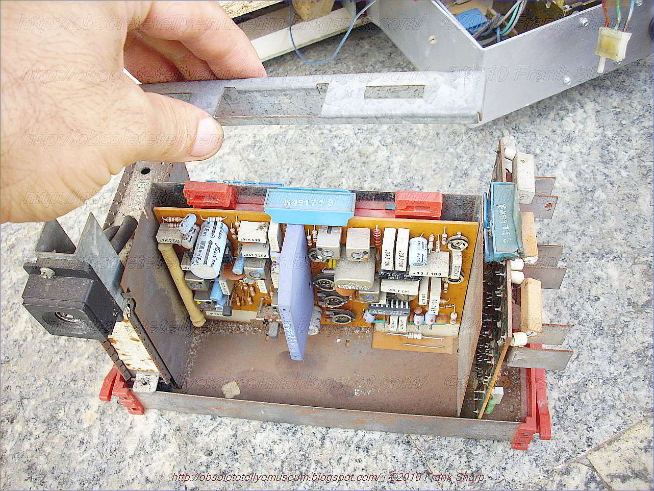
The SINUDYNE 2969 COLOR CHASSIS FR2 PROFESSIONAL 1000 is an excellent example of organization of a tv color chassis.
His full grouped multi modular concept is pretty unique and is rendering service and analisys of tv circuits easy and pleasant.
On the left side a group of signal units is present.
The power supply is located In the middle bottom side.
Right side the group of all deflections units and EHT parts.
The chassis shown is an example on how good was Italian engineering and industry and even if wasn't anyway capable to compete with the bigs it had anyway his limited but present role and fashion.
SINUDYNE 2969 COLOR CHASSIS FR2 PROFESSIONAL 1000 UNITS:
- SIGNAL GROUP BASE BOARD 8C-A-00 FR2
- RGB AMPLIFIER M-FV-00 0959000 FR2
- CHROMINANCE UNIT M-CR-00 0962000 FR2 TBA560C TBA550 TBA540
- IF AMPL DEM UNIT M-MF-00 0958000 FR2 TBA440
- IF SOUND + AMPL TBA120T M-MS-00 0963000 FR2
- DEFLECTION GROUP BASE BOARD PCB BC-B-00 FR2
- HOR OSC SYNCH M-00-00 0967000 FR2 TBA920
- FRAME VERTICAL OSCILLATOR UNIT M-OV-OO 0965000 FR2
- E/W + N/S CORRECTION UNIT M-RA-00 0969000
- SUPPLY UNIT M-AL-00 0970000 FR3.
 THE
TBA920 SYNC/TIMEBASE IC It has been quite common for some time for sync
separation to be carried out in an i.c. but until 1971 this was as far
as i.c.s had gone in television receiver timebase circuitry. With the
recent introduction of the delta featured 110° colour series however
i.c.s have gone a step farther since this chassis uses a TBA920 as sync
separator and line generator. A block diagram of this PHILIPS /Mullard
i.c. is shown in Fig. 1.
THE
TBA920 SYNC/TIMEBASE IC It has been quite common for some time for sync
separation to be carried out in an i.c. but until 1971 this was as far
as i.c.s had gone in television receiver timebase circuitry. With the
recent introduction of the delta featured 110° colour series however
i.c.s have gone a step farther since this chassis uses a TBA920 as sync
separator and line generator. A block diagram of this PHILIPS /Mullard
i.c. is shown in Fig. 1.The video signal at about 2-7V peak -peak is fed to the sync separator section at pin 8, the composite sync waveform appearing at pin 7.
The noise gate switches off the sync separator when a positive -going input pulse is fed in at pin 9, an external noise limiter circuit being required .
The line sync pulses are shaped by R1 /C1 /C2/R2 and fed in to the oscillator phase detector section at pin 6.
The line oscillator waveform is fed internally to the oscillator phase detector circuit which produces at pin 12 a d.c. potential which is used to lock the line oscillator to the sync pulse frequency, the control potential being fed in at pin 15. The oscillator itself is a CR type whose waveform is produced by the charge and discharge of the external capacitor (C7) connected to pin 14. The oscillator frequency is set basically by C7 and R6 and can be varied by the control potential appearing at pin 15 from pin 12 and the external line hold control. Internally the line oscillator feeds a triangular waveform to the oscillator and flyback phase detector sections and the pulse width control section. The coincidence detector section is used to set the time constant of the oscillator phase detector circuit. It is fed internally with sync pulses from the sync separator section, and with line flyback pulses via pin 5. When the flyback pulses are out of phase with the sync pulses the impedance looking into pin 11 is high (21(Q). When the pulses are coincident the impedance falls to about 150Q and the oscillator phase detector circuit is then slow acting. The effect of this is to give fast pull -in when the pulses are out of sync and good noise immunity when they are in sync. The coincidence detector is controlled by the voltage on pin 10. When the sync and flyback pulses are in sync C3 is charged: when they are out of sync C3 discharges via R3. VTR use has been taken into consideration here. With a video recorder it is necessary to be able to follow the sync pulse phase variations that occur as a result of wow and flutter in the tape transport system, while noise is much less of a problem. For use with a VTR therefore the network on pin 10 can simply be left out so that the oscillator phase detector circuit is always fast acting. A second control loop is used to adjust the timing of the pulse output obtained from pin 2 to take into account the delay in the line output stage. The fly back phase detector compares the frequency of the flyback pulses fed in at pin 5 with the oscillator signal which has already been synchronised to the sync pulse frequency.
Any phase difference results in an output from pin 4 which is integrated and fed into the pulse width control section at pin 3. The potential at pin 3 sets the width of the output pulse obtained at pin 2: with a high positive voltage (via R11 and R12) at pin 3 a 1:1 mark -space ratio out- put pulse (32/us on, 32/us off) will be produced while a low potential at pin 3 (negative output at pin 4) will give a 16us output pulse at the same frequency. The action of this control loop continues until the fly- back pulses are in phase with a fixed point on the oscillator waveform: the flyback pulses are then in phase with the sync pulses and delays in the line output stage are compensated. The output obtained at pin 2 is of low impedance and is suitable for driving valves, transistors or thyristors: R9 is necessary to provide current limiting.
SINUDYNE 2969 COLOR CHASSIS FR2 PROFESSIONAL 1000 power supply CONSTANT-VOLTAGE CONVERTER EMPLOYING THYRISTOR:
A constant voltage converter having a rectifier for rectifying AC power and with a thyristor connected between the rectifier and a filter for selectively passing therethrough a rectified output to an output terminal. There is a wave generator connected to the output of the rectifier for producing a first signal and an intergrator circuit connected to the output of the wave generator for producing an integral output in response to this first signal. In addition there is a detector circuit for detecting a fluctuation of the rectified output power and for producing second signal. A comparison circuit is connected between the intergrator circuit and the detector circuit for producing third signal in accordance with the comparison. A trigger circuit is connected between the comparison circuit and the control gate of the thyristor for supplying a phase control signal to the thyristor to thereby obtain a constant voltage output regardless of the fluctuation of the rectified output.
Description:
This invention relates to constant-voltage converters and more particularly to a constant-voltage converter employing a thyristor.Conventional constant-voltage converters of the type employing a thyristor are arranged to phase shift and full-wave-rectify an input a.c. power applied thereto and to maintain the output voltages constant by regulating the firing angle of the thyristor in comparison of the output voltages with the phase-shifted and rectified input a.c. power. When, however, these converters are connected to a common a.c. source having a relatively high internal impedance, the waveform of the phase-shifted and rectified a.c. input power is distorted thereby causing undesired operations of the converters.
It is therefore an object of the present invention to provide a constant-voltage converter which correctly operates notwithstanding the distortion of the input a.c. voltage.
Another object of the invention is to provide a constant-voltage converter which effectively suppress an undesired rush current.
Another object of the invention is to provide a constant-voltage converter having an improved feed-back circuit of a substantially constant loop gain .
In the drawings:
FIG. 1 is a schematic view of a converter according to the present invention;
FIG. 2 is a diagram showing a circuit arrangement of the converter of FIG. 1;
FIG. 3 is a diagram showing various waveforms of signals appearing in the circuit of FIG. 2;
FIG. 4 is a diagram showing various waveforms appearing in the circuit of FIG. 2 when an a.c. power is supplied to the circuit;
FIG. 5 is a diagram showing another circuit arrangement of the converter of FIG. 1;
FIG. 6 is a diagram showing waveforms of signals appearing in the circuit of FIG. 5; and
FIG. 7 is a diagram showing further another circuit arrangement of generator the of FIG. 1.
Referring now to FIG. 1, a cons
 tant-voltage converter 10 according to the present invention comprises a rectifier 11 having two input terminals 12 and 13 through which an a.c. power is supplied. The rectifier 11 is preferably a full-wave rectifier although a half-wave rectifier may be employed. An output 14 of the rectifier 11 is connected through a line 15 to an anode of a thyristor 16. The thyristor 16 passes therethrough the rectified a.c. power in only one direction from its anode to cathode when triggered by a trigger pulse through its gate. The cathode of the thyristor 16 is connected through a line 17 to an input of a smoothing filter 18. The smoothing filter 18 smoothes the power from the thyristor 16. An output of the smoothing filter 18 is connected through a line 19 to an output terminal 20. The output 14 of the rectifier 11 is also connected through a line 21 to a saw-tooth wave generator 22 which generates a saw-tooth wave signal having the same repetition period as the rectified input a.c. power. An output of the saw-tooth wave generator 22 is connected through a line 23 to one input of a trigger pulse generator 24. The other input of the trigger pulse generator 24 is connected through a line 25 to the line 19. An output of the trigger pulse generator 24 is connected through a line 26 to the gate of the thyristor 16. The trigger pulse generator 24 produces a trigger pulse on its output when the voltage of the saw-tooth wave signal reaches a level which is varied in response to the output voltage on the terminal 20. The trigger pulse generator 24 may be variously arranged and in this case arranged to comprise rectangular generator 27 having one input connected through the line 23 to the saw-tooth wave generator 22 and the other input connected through a line 28 to an output voltage detector 29. The detector 29 produces a reference signal representing the output voltage on the terminal 20. The pulse generator 27 is adapted to produces a rectangular pulse when the saw-tooth wave signal to the one input reaches a level which defined is in accordance with the reference signal. An output of the rectangular pulse generator 27 is connected through a line 30 to an input of a trigger circuit 31. The trigger circuit 31 is adapted to convert the rectangular pulse into a spike pulse. An output of the trigger circuit 31 is connected through the line 26 to the gate of the thyristor 16.
FIG. 2 illustrates a prefe
 rred circuit arrangement of the converter shown in FIG. 1 which comprises a rectifier 11 of a full-wave rectifier consisting of rectifiers 40, 41, 42 and 43. Inputs of the rectifier are connected to terminals 12 and 13 through which an a.c. power is applied. The output 14 of the rectifier 11 is connected through a line 15 to an anode of a thyristor 16. A cathode of the thyristor 16 is connected through a line 17 to a smoothing filter 18 which includes a capacitor C4 having one terminal connected to the line 17 and the other terminal grounded. The output of the smoothing filter 18 is connected through a line 19 to an output terminal 20.
The rectangular pulse generator 27 comprises a transistor T 2 of PNP type having a base connected through a resistor R 6 to the collector of the transistor T 1 . An emitter of the transistor T 2 is connected through a resistor R 7 to the emitter of the transistor T 1 . A collector of the transistor T 2 is grounded through a resistor R 8 and connected through the line 30 to one terminal of a capacitor C 4 of the trigger circuit 31. The other terminal of the capacitor C 4 is connected through a line 26 to the gate of the thyristor 16.
The output voltage detector 29 includes a transistor T 3 of NPN type having an emitter grounded through a zener diode ZD. A collector of the transistor T 3 is connected through a line 28 to the emitter of the transistor T 2 and, on the other hand, connected through a capacitor C 5 to the grounded. A base of the transistor T 3 is connected to a tap of an adjustable resistor R 9 connected through a resistor R 10 and a line 25 to the line 19 and connected, in turn, to the ground through a resistor R 11 .
When, in operation, an a.c. electric power is applied through the input terminals 12 and 13 of the rectif
 ier 11, a full-wave rectified power as shown in FIG. 3 (a) appears on the output 14. The rectified power is applied through the line 15 to the anode of the thyristor 16. The thyristor 16 passes therethrough the rectified power while its firing angle is regulated by the trigger signal applied to the gate. The rectified power passed through the thyristor 16 is applied through the line 17 to the smoothing filter 18. The smoothing filter smoothes the power by removing the ripple component in the power. The smoothed power appears on the line 19 which is to be supplied to a load through the output terminal 20. The smoothed power on the line 19 is, on the other hand, delivered through the line 25 to the resistor R 10 of the output voltage detector 29. The resistor R 10 constitutes a voltage divider in cooperation with the resistors R 9 and R 11 . The output of the voltage divider is applied through the tap of the resistor R 9 to the base of the transistor T 3 . When the potential of the base of the transistor T 3 exceeds the zener voltage of the zener diode ZD, a base current flows through the transistor T 3 so as to render the transistor T 3 conductive. The potential of the collector of the transistor T 3 then varies in accordance with the voltage of the smoothed output power on the line 19. The potential variation at the collector of the transistor T 3 is then applied through the line 28 to the trigger pulse generator 27 and utilized to regulate the triggering timing of the thyristor 16.
The full-wave rectified power is, on the other hand, applied through the line 21 to the saw-tooth wave generator 22. Since the resistors R 1 and R 2 consistute a voltage divider to reduce the voltage of the full-wave rectified power to a potential at the junction J 1 , a charging current to the capacitor C 1 flows from the emitter to the base of the transistor T 1 whereby the transistor T 1 repeats ON-OFF operation in accordance with the voltage of the rectified power. If the transistor T 1 is conductive when the voltage of the full-wave rectified power is lower than a threshold voltage v 1 as shown in FIG. 3(a), then the potential at the collector of the transistor T 1 is varied as shown in FIG. 3 (b) due to the charge and discharge of the capacitor C 2 . The variation of the potential at the collector of the transistor T 1 is supplied through the line 23 to the resistor R 6 of the trigger pulse generator 27.
As long as the voltage of the smoothed power on the line 19 equals to the rated output voltage, the transistor T 2 is adapted to become conductive when the voltage of the saw-tooth wave signal falls below a threshold value v 3 shown in FIG. 3(b). Therefore, a potential at the collector of the transistor T 2 varies as shown in FIG. 3(c). The potential variation, that is, a pulse signal at the collector of the transistor T 2 is supplied through the line 30 to the capacitor C 4 of the trigger circuit trigger 31. The trigger circuit 31 converts the pulse signal into a spike pulse or a trigger pulse shown in FIG. 3(d) which is then applied through the line 25 to the gate of the thyristor 16. Upon receiving the spike pulse, the thyristor 16 becomes conductive until the voltage of the rectified power on the line 15 falls below the cut-off voltage of the thyristor 16.
When the voltage of the smoothed power on the line 19 exceeds the rated output voltage, the collector current of the transistor T 3 increases with the result that the current flowing through the resistor R 7 increases. The threshold voltage of the transistor T 2 therefore reduces to a voltage v 2 as shown in FIG. 3(b). At this instant, leading edge of the pulse signal delays as shown by dot-and-dash lines in FIG. 3(c), so that each trigger pulse delays as shown by dot-and-dash line in FIG. 3(d). When on the contrary, the voltage of the smoothed signal on the line 19 lowers below the rated output voltage, the collector current of the transistor T 3 decreases whereby the threshold voltage rises to a voltage v 4 in FIG. 3(b). Each leading edge of the signal pulse now leads as shown by dotted line in FIG. 3(d). Being apparent from the above description, the appearance timing of each trigger pulse is regulated in accordance with the voltage of the smoothed power on the line 19 so that the voltage of the output voltage at the terminal 20 is held substantially constant.
Referring now to FIG. 4, start operation of the converte
 r 10 is discussed hereinbelow in conjunction with FIG. 2. When an a.c. voltage is applied to the input terminals 12 and 13, the capacitor C 3 begins to be charged by the voltage on the line 15, and the capacitor C 5 also begins to be charged through the resistors R 3 and R 7 . It is important that the time constant of power supply circuit constituted by the resistor R 3 and the capacitor C 3 is selected to be much larger than that of the time constant of another power supply circuit constituted by the resistor R 7 and the capacitor C 5 . Thus, the emitter potential of the transistor T 1 is built up more quickly than that of the transistor T 2 . Upon completion of the charging of the capacitor C 3 , the saw-tooth wave generator 22 begins to generate saw-tooth wave signal as shown in FIG. 4(b). Since the capacitor C 5 is, on the other hand, slowly charged, the emitter voltage of the transistor T 2 slowly rises as shown in FIG. 4(c), so that, the threshold voltage of the transistor T 2 gradually rises as shown by a dotted line in FIG. 4 (b). Accordingly, the trigger pulses is produced on the gate of the thyristor 16 as shown in FIG. 4(d), whereby the firing angle of the thyristor 16 is gradually reduced as shown in FIG. 4(a) which illustrates the voltage at the output terminal 14 of the rectifier 11. The output voltage on the output terminal 20 therefore gradually rise up as shown in FIG. 4(e). It is to be understood that since the output voltage of the converter 10 starts to gradually rise up as shown in FIG. 4(e), an undesired rush current is effectively suppressed.
FIG. 5 illustrates another fo
 rm of the converter 10 which is arranged identically to the circuit arrangement of FIG. 1 except that an integrator 50 is interposed between the output of the saw-tooth wave generator 22 and the input of the trigger pulse generator 27. The integrator 50 includes a resistor R 12 having one terminal connected to the output of the saw-tooth wave generator 22 and the other terminal connected to the input of the rectangular pulse generator 27, and a capacitor C 7 having one terminal connected to the other terminal of the resistor R 12 and the other terminal grounded.
In operation, the saw-tooth wave generator 22 produces on its ouput a saw-tooth wave signal having decreasing exponential wave form portion as shown in FIG. 6 (a), although the saw-tooth wave signal ideally is illustrated in FIG. 3. This saw-tooth wave signal is converted by the integrator 50 into another form of saw-tooth wave having a increasing exponential wave form portion as shown in FIG. 6(b).
It should be noted that the saw-tooth wave signal of FIG. 6(a) has a smaller inclination near 180°. Hence, when the integrator 50 is omitted and the saw-tooth wave signal as shown in FIG. 6(a) is applied to the trigger pulse generator 27, the rate of change of the output voltage of the converter 10 become larger at a firing angle near to 1
 80°. On the other hand, it is apparent from FIG. 6(c) that the rate of change the output voltage of the thyristor 16 with respect to the firing angle become large at a firing angle near to 180°. Therefore, the loop gain of the trigger pulse generator 24 increases when the firing angle of the thyristor 16 is near to 180°. It is apparent through a similar discussion that the loop gain of the trigger pulse generator 24 decreases when the firing angle is near to 90°. Such non-uniformity of the loop gain of the trigger pulse generator invites a difficulty of the regulation of the output voltage of the converter. It is to be noted that the saw-tooth wave signal shown in FIG. 6(b) has a large inclination at an angle near 180°. Therefore, when the saw-tooth wave signal of FIG. 6(b) is applied to the trigger pulse generator 24, the loop gain of the trigger pulse generator 24 is held substantially constant, whereby the output voltage of the converter is effectively held constant.
It is to be understood that the integrator 50 may be substituted for by a miller integrator and a bootstrap integrator. Furthermore, a plurality of integrator may be employed, if desired.
FIG. 7 illustrates another circuit arrangement of the converter according to the present invention, which is arranged identically to the circuit of FIG. 2 except for the trigger circuit 31 and the smoothing circuit 18.
The trigger circuit 31 of FIG. 7 comprises a transformer TR with primary and secondary coils. One terminal of the primary coil is connected to the resistor R 7 of the pulse generator 27. The other terminal of the primary coil is connected to a collector of a transistor T 4 of NPN type. The secondary coil has terminals respectively connected to the gate and cathode of the thyristor 16. An emitter of the transistor T 4 is grounded through a resistor R 13 . A base of the transistor T 4 is grounded through a resistor R 14 and connected through a capacitor C 8 to the collector of the transistor T 2 of the pulse generator 27.
The smoothing filter 18 of FIG. 7 comprises a choke coil CH connected to the lines 17 and 19, and to capacitors C 9 and C 10 which are in turn grounded. The circuit of FIG. 7 operates in the same manner as the circuit of FIG. 2.
Obviously many modifications and variations of the present invention are possible in the light of the above teachings. It is therefore to be understood that within the scope of the appended claims the invention may be practiced otherwise than as specifically described.
The CRT TUBE IS a TELEFUNKEN A66-410X.
SINUDYNE 2969 COLOR CHASSIS FR2 PROFESSIONAL 1000 NORD SOUTH (NORD/SUD) CORRECTION CIRCUIT ARRANGEMENT FOR CORRECTING THE DEFLECTION OF AT LEAST ONE ELECTRON BEAM IN A TELEVISION PICTURE TUBE BY MEANS OF A TRANSDUCTOR :
A circuit arrangement for raster correction in a television picture tube by means of a transductor whose power winding is connected in parallel with at least a portion of the line deflection coils, the line deflection genera
 tor having a low internal impedance. In order to increase this impedance a mainly inductive impedance is connected in series with the generator. In a picture tube employing at least two electron beams the series impedance may include the convergence circuit. As a result the convergence in the corners of the picture screen is also improved. The linearity control circuit may likewise form part of the series impedance.
1. A deflection circuit for a cathode ray tube comprising a transistor horizontal deflection generator; a horizontal deflection coil parallel coupled to said generator; means for pincushion correction of said tube comprising a saturable reactor having a control winding adapted to receive a vertical deflection signal and a power winding parallel coupled to at least a portion of said deflection coil; and means for increasing the effectiveness of said correction means comprising an impedance element external to said generator having a substantially inductive reactance series coupled between said generator and said coil. 2. A circuit as claimed in claim 1 wherein said generator comprises a transformer having a tap and said power winding has a first end coupled to said coil and a second end coupled to said tap. 3. A circuit as claimed in claim 1 wherein said impedance element comprises means for controlling the linearity of the beam deflection. 4. A deflection circuit for a cathode ray tube having at least two electron beams comprising a transistor horizontal deflection generator; a horizontal deflection coil parallel coupled to said generator; means for pincushion correction of said tube comprising a saturable reactor having a control winding adapted to receive a vertical deflection signal and a power winding parallel coupled to at least a portion of said deflection coil; means for increasing the effectiveness of said correction means comprising an Impedance element external to said generator having a substantially inductive reactance series coupled between said generator and said coil; and means for dynamically converging said beams comprising a convergence circuit coupled to said horizontal generator and to said transductor. 5. A circuit as claimed in claim 4 wherein said generator comprises a transformer having a tap and said power winding has a first end coupled to said coil and a second end coupled to said tap. 6. A circuit as claimed in claim 4 wherein said impedance element comprises means for controlling the linearity of the beam deflection.
The invention relates to a circuit arrangement for correcting the deflection of at least one electron beam (raster correction) in a television picture tube by means of a saturable reactor a power winding of which is connected in parallel with at least a portion of the coils for the horizontal deflection, the current flowing through these coils being supplied by a deflection generator having a low internal impedance.
A circuit arrangement for raster correction with the aid of a transductor is described, for example, in U.S. Pat. No. 3,444,422. In this patent the power winding of a transductor is connected in parallel with the horizontal deflection coils while the control winding receives a signal of field frequency so that the current of line frequency which flows through the deflection coils is modulated at the field
 -frequency (East-West correction), whereas the vertical deflection current is modulated at the line frequency (North-South correction). However, in this known arrangement there is the difficulty that the transductor can exert little influence on the horizontal deflection current if the internal impedance of the deflection generator is low because the transductor then only constitutes an additional load on the generator. This is the case when the deflection generator includes a valve with feedback -- or a switch formed with one or more transistors. In order to be able to use a transductor arrangement also in such a case the circuit arrangement according to the invention is characterized in that a mainly inductive impedance is connected in series between the said parallel arrangement and the deflection generator.
 Due to the step according to the invention the internal impedance of the deflection generator is increased and the different components of the circuit remain mainly inductive so that the deflection current is more or less linear when the voltage provided by the deflection generator during the line scan period is substantially constant. The series impedance may be, for example, a fixed coil. However, the invention is furthermore based on the recognition of the fact that the increase in the internal resistance of the horizontal deflection generator may not only be obtained by a constant impedance, but other arrangements envisaging other improvements of the deflection may be used for this purpose. In that case even special improvements may be obtained as will be apparent hereinafter and possible small non-linearities of the additionally used arrangements have no detrimental results.
 It is true that in known convergence circuits in picture tubes employing a plurality of electron beams a satisfactory improvement is obtained for the central horizontal and vertical lines of a picture tube of the shadow mask type. However, it is found that convergence errors may subsist in the corners of the picture. Known circuit arrangements which correct these second-order errors are often complicated and expensive. In the circuit arrangement according to the invention a satisfactory compensation of such convergence errors is possible in a simple manner if the series impedance which is arranged between the horizontal deflection generator and the deflection coils includes the convergence circuit. In this manner the sum of the deflection current and of the current derived for the field correction and modulated by the transductor flows through the convergence circuit so that the desired additional convergence correction in the corners of the written raster is obtained.
In order that the invention may be readily carried into effect a few embodiments thereof will now be described in detail by way of example with reference to the accompanying diagrammatic drawings in which:
FIG. 1 shows a circuit arrangement in which the transductor is connected in parallel with the deflection coils, while in
FIG. 2 the transductor is only fed by part of the voltage applied to the deflection coils.
FIG. 1 shows two line-output transistors 1 and 2 which are arranged in series. The emitter of transistor 2 is connected to ground through a winding 3 while the collector of transistor 1 is connected through a winding 4 and a small series impedance 5, preferably a resistor, to the positive terminal of a supply source V b whose negative terminal is connected to ground.
Windings 3 and 4 are wound together with an EHT-winding 6 on the same transformer core 7. The ends of windings 3 and 4 remote from each other are connected through the capacitor 10 for the S-correction to the deflection-unit consisting of two windings 8 and 9 arranged, for example, in parallel. The base of transistors 1 and 2 receive pulses of line frequency in a manner not shown in FIG. 1 so that these transistors are cut off during the flyback period. During the scan period, a substantially constant voltage is applied to the deflection unit. Consequently a more or less sawtooth-shaped current flows through windings 8 and 9. The bipartite power winding 11 of a transductor ensuring the raster correction is connected in parallel with this deflection unit 8, 9. The control winding 12 of said transductor, and a converting capacitor 13 in parallel therewith form part of the circuit for the vertical deflection through terminals 14 and 15. An adjustable coil 16 with which the raster correction can be adjusted exactly is connected in series with winding 12.
Windings 3 and 4 have the same number of turns so that pulses of the same amplitude and reversed polarity are produced at the emitter of transistor 2 and at the collector of transistor 1. As a result a disturbing radiation of these pulses is reduced. Furthermore, transistor types are chosen in this Example for transistors 1 and 2 whose collector-base diodes may function as efficiency diodes. All this has been described in U.S. Pat. No. 3,504,224.
According to the invention the convergence circuit 17 is arranged through a separation transformer 20 between the end of winding 3 remote from winding 4 and the horizontal deflection coils 8, 9. Furthermore, this current branch includes the linearity control circuit 21 which comprises the parallel arrangement of a resistor and a coil whose inductance is adjustable, for example, by means of premagnetization of the core of the coil. A current, which is the sum of the current for the deflection coils 8, 9 and of the current for the power winding 11 of the transductor, flows through the primary winding of transformer 20. This primary current is transformed to the secondary circuit of transformer 20 so that a current flows through convergence circuit 17.
In known arrangements the con
vergence current is only influenced by the deflection current itself. It has been found that in this case the convergence correction is not sufficient in the corners of the picture. At these areas, where the deflection in both directions is at a maximum, a greater intensity of the convergence current is required. This is especially the case in picture tubes having a great deflection angle and according to the invention this is achieved in that the current which is derived from the power winding 11 of the transductor for the raster correction is also applied to the convergence circuit. This current flows from the horizontal deflection generator constituted by windings 3 and 4 through the primary winding of transformer 20 to power winding 11 of the transductor. The transductor current is in fact at a minimum in the center of the picture and increases towards the edges and particularly towards the corners. Thus the convergence current varies in the desired manner. According to the invention the desired improvements of the convergence correction and simultaneously the likewise desired increase in the internal resistance of the horizontal deflection generator is consequently obtained without a considerable increase in the number of required circuit elements and without disturbing the normal operation of the circuit arrangement. Due to transformer 20 a terminal of convergence circuit 17 may be connected to ground so that the convergence can be adjusted safely. If necessary, a suitable impedance transformation may also be obtained with the aid of transformer 20.
 The linearity control circuit 21 may alternatively be connected in series with the said branch which includes transformer 20. As a result the internal resistance of the horizontal deflection generator for the line frequency is further increased without the field correction and the convergence correction being disturbingly influenced.
FIG. 2 shows a modification of the circuit arrangement according to the invention in which the deflection current is not changed relative to that of FIG. 1. The end of power winding 11 of the transductor shown on the upper side of FIG. 1 is connected to ground in FIG. 2. In addition convergence circuit 17 is included between winding 3 and ground so that separation transformer 20 may be omitted. If as a first approximation the impedances 5 and 17 are assumed to be negligibly small relative to the other impedance of the circuit arrangement, power winding 11 may be considered to be connected to a tap on the deflection generator 3, 4. Consequently, only approximately half the voltage of the deflection generator is applied to transductor winding 11 which winding must therefore be proportioned in such a manner that it can convey a current which is approximately twice as large as that of FIG. 1. This larger current also flows through convergence circuit 17 which, with the omission of separation transformer 20, is favorable for the convergence in the corners of the picture screen.
In FIG. 2 the emitter of transistor 2 is connected to ground i.e., the said tap on the deflection generator. During the scan period the series arrangement of supply source V b and windings 3 and 4 FIG. 1 is substantially short-circuited by transistors 1 and 2. In order that these transistors in the circuit arrangement according to FIG. 2 operate under the same circumstances as those in FIG. 1, an additional winding 24 must be wound on core 7 between windings 4 and 6, winding 24 having the same number of turns as winding 3, and the collector of transistor 1 must be connected to the junction of windings 6 and 24.
The end of power winding 11 connected to ground in FIG. 2 may alternatively be connected for the desired adjustment of the corner convergence to a different tap on the transformer, that is to say, on winding 3 or 4.
Resistor 5 serves in known manner mainly as a safety resistor so that in case of an inadmissible load of the EHT, for example, as a result of flash-over in the picture tube, the supply voltage for transistors 1 and 2 is reduced so that overload of these transistors is avoided.
A circuit arrangement for raster correction with the aid of a transductor is described, for example, in U.S. Pat. No. 3,444,422. In this patent the power winding of a transductor is connected in parallel with the horizontal deflection coils while the control winding receives a signal of field frequency so that the current of line frequency which flows through the deflection coils is modulated at the field
In order that the invention may be readily carried into effect a few embodiments thereof will now be described in detail by way of example with reference to the accompanying diagrammatic drawings in which:
FIG. 1 shows a circuit arrangement in which the transductor is connected in parallel with the deflection coils, while in
FIG. 2 the transductor is only fed by part of the voltage applied to the deflection coils.
FIG. 1 shows two line-output transistors 1 and 2 which are arranged in series. The emitter of transistor 2 is connected to ground through a winding 3 while the collector of transistor 1 is connected through a winding 4 and a small series impedance 5, preferably a resistor, to the positive terminal of a supply source V b whose negative terminal is connected to ground.
Windings 3 and 4 are wound together with
an EHT-winding 6 on the same transformer core 7. The ends of windings 3 and 4 remote from each other are connected through the capacitor 10 for the S-correction to the deflection-unit consisting of two windings 8 and 9 arranged, for example, in parallel. The base of transistors 1 and 2 receive pulses of line frequency in a manner not shown in FIG. 1 so that these transistors are cut off during the flyback period. During the scan period, a substantially constant voltage is applied to the deflection unit. Consequently a more or less sawtooth-shaped current flows through windings 8 and 9. The bipartite power winding 11 of a transductor ensuring the raster correction is connected in parallel with this deflection unit 8, 9. The control winding 12 of said transductor, and a converting capacitor 13 in parallel therewith form part of the circuit for the vertical deflection through terminals 14 and 15. An adjustable coil 16 with which the raster correction can be adjusted exactly is connected in series with winding 12.Windings 3 and 4 have the same number of turns so that pulses of the same amplitude and reversed polarity are produced at the emitter of transistor 2 and at the collector of transistor 1. As a result a disturbing radiation of these pulses is reduced. Furthermore, transistor types are chosen in this Example for transistors 1 and 2 whose collector-base diodes may function as efficiency diodes. All this has been described in U.S. Pat. No. 3,504,224.
According to the invention the convergence circuit 17 is arranged through a separation transformer 20 between the end of winding 3 remote from winding 4 and the horizontal deflection coils 8, 9. Furthermore, this current branch includes the linearity control circuit 21 which comprises the parallel arrangement of a resistor and a coil whose inductance is adjustable, for example, by means of premagnetization of the core of the coil. A current, which is the sum of the current for the deflection coils 8, 9 and of the current for the power winding 11 of the transductor, flows through the primary winding of transformer 20. This primary current is transformed to the secondary circuit of transformer 20 so that a current flows through convergence circuit 17.
In known arrangements the con
FIG. 2 shows a modification of the circuit arrangement according to the invention in which the deflection current is not changed relative to that of FIG. 1. The end of power winding 11 of the transductor shown on the upper side of FIG. 1 is connected to ground in FIG. 2. In addition convergence circuit 17 is included between winding 3 and ground so that separation transformer 20 may be omitted. If as a first approximation the impedances 5 and 17 are assumed to be negligibly small relative to the other impedance of the circuit arrangement, power winding 11 may be considered to be connected to a tap on the deflection generator 3, 4. Consequently, only approximately half the voltage of the deflection generator is applied to transductor winding 11 which winding must
therefore be proportioned in such a manner that it can convey a current which is approximately twice as large as that of FIG. 1. This larger current also flows through convergence circuit 17 which, with the omission of separation transformer 20, is favorable for the convergence in the corners of the picture screen.In FIG. 2 the emitter of transistor 2 is connected to ground i.e., the said tap on the deflection generator. During the scan period the series arrangement of supply source V b and windings 3 and 4 FIG. 1 is substantially short-circuited by transistors 1 and 2. In order that these transistors in the circuit arrangement according to FIG. 2 operate under the same circumstances as those in FIG. 1, an additional winding 24 must be wound on core 7 between windings 4 and 6, winding 24 having the same number of turns as winding 3, and the collector of transistor 1 must be connected to the junction of windings 6 and 24.
The end of power winding 11 connected to ground in FIG. 2 may alternatively be connected for the desired adjustment of the corner convergence to a different tap on the transformer, that is to say, on winding 3 or 4.
Resistor 5 serves in known manner mainly as a safety resistor so that in case of an inadmissible load of the EHT, for example, as a result of flash-over in the picture tube, the supply voltage for transistors 1 and 2 is reduced so that overload of these transistors is avoided.
SINUDYNE 2969 COLOR CHASSIS FR2 PROFESSIONAL 1000 E/W CORRECTION Circuit arrangement in an image display apparatus for (horizontal) line deflection:
Line deflection circuit in which the deflection coil is east-west modulated. In order to cancel an east-west dependent horizontal linearity defect the inductance value of the linearity correction coil is made independent of the field frequency, for example by means of a compensating current. In an embodiment this current is supplied by the shunt coil of the east-west modulator.
1. Circuit arrang
Description:
The invention relates to a circuit arrangement in an image display apparatus for (horizontal) line deflection, which apparatus also includes a circuit arrangement for (vertical) field deflection, provided with a generator for generating a sawtooth line-frequency deflecting current through a line deflection coil and with a modulator for field-frequency modulation of this current, the deflection coil being connected in series with a linearity correction coil in the form of an inductor having a bias-magnetized core.
By means of the linearit
y correction coil the linearity error due to the ohmic resistance of the deflection circuit is corrected. The sign of the bias magnetisation is chosen so that it is cancelled by the deflection current at the beginning of the deflection interval, so that the inductance of the correction coil is a maximum, whereas the voltage drop across the deflection coil then is a minimum. This voltage drop is adjustable by adjustment of the starting inductance of the correction coil. During the deflection interval the core gradually becomes saturated so that the inductance of, and the voltage drop across, the correction coil decrease. Thus the linearity error can be cancelled exactly at the beginning of the interval, that is to say on the left on the screen of the image display tube, and with a certain approximation at other locations.
In image display tubes using a large deflection angle, raster distortion, which generally is pincushion-shaped, of the image displayed occurs. This distortion can be removed in the horizontal direction, the so-called east-west direction, by means of field-frequency modulation of the line deflection current, the envelope in the case of pincushion-shaped distortion being substantially parabolic so that the amplitude of the line deflection current is a maximum at the middle of the field deflection interval.
It
was found in practice that the said two corrections are not independent of one another, that is to say the adjustment of the east-west modulation affects horizontal linearity. As long as the modulation depth is not excessive, a satisfactory compromise can be found. However, in display tubes having a deflection angle of 110° and particularly in colour display tubes in which the deflection coils have a converging effect also, it is difficult to find such a compromise. A tube of this type is described in "Philips Research Reports," volume Feb. 14, 1959, pages 65 to 97; the distribution of the deflection field is such that throughout the display screen the landing points of the electron beams coincide without the need for a converging device. Owing to this field distribution, however, the pin-cushion-shaped distortion in the image displayed in the east-west direction is greater than in comparable display tubes of another type. Hence there must be east-west modulation of the line deflection current to a greater depth. It is true that under these conditions horizontal linearity can correctly be adjusted over a given horizontal strip after the east-west modulation has been adjusted correctly, i.e., for a rectangular image, but it is found that in other parts of the display screen a serious linearity error remains. When vertical straight lines are displayed as straight lines in the right-hand part of the screen, they are displayed as curved lines in the left-hand part.
The invention is based on the recognition that the defect to be removed is due to a field-frequency variation of the said inductance because the latter is current-dependent. According to a further recognition of the invention the circuit arrangement is characterized in that it includes a current supply source for producing a compensating line-frequency sawtooth current through a winding of the linearity correction coil, the amplitude of the current being field-frequency modulated. The circuit arrangement according to the invention may further be characterized in that an additional winding is provided on the core of the linearity correction coil and is traversed by the compensating current. A circuit arrangement in which the modulator for modulating the line deflection current includes a compensation or bridge coil may according to the invention be characterized in that the additional winding is connected in series with the said coil.
The invention also relates to a linearity correction coil for use in a line deflection circuit having a core which is made of a magnetic material and is bias magnetized by at least one permanent magnet, which coil is characterized in that an additional winding is provided on the core.
Embodiments of the invention will now be described by way of example, with reference to the accompanying diagrammatic drawings, in which
FIG. 1 is the circuit diagram of a known circuit arrangement for line deflection in which the line deflection current is east-west modulated,
FIG. 2 shows the distorted image which is displayed on the screen when the circuit arrangement of FIG. 1,
FIG. 3 is a graph explaining the observed defect, and
FIGS. 4 and 7 show embodiments of the circuit arrangement according to the invention by which this defect can be cancelled.
FIG. 1 is a greatl simplified circuit diagram of a line deflection circuit of an image display apparatus, not shown further. The circuit includes the series combination of a line deflection coil L y , a linearity correction coil L and a trace capacitor C t , which series combination is traversed by the line deflection current i y . The collector of an npn switching transistor T r and one end of a choke coil L 1 are connected to a junction point A of a diode D, a capacitor C r and the said series combination. The other end of the choke coil is connected to the positive terminal of a supply voltage source which supplies a substantially constant direct voltage V b and to the negative terminal of which the emitter of transistor Tr is connected. This negative terminal may be connected to earth. The other junction point B of elements D and C r and of the series combination of elements C t , L y and L is connected to one terminal of a modulation source M for east-west correction which has its other terminal connected to earth. Diode D has the pass direction shown in the FIG.
 simplified circuit diagram of a line deflection circuit of an image display apparatus, not shown further. The circuit includes the series combination of a line deflection coil L y , a linearity correction coil L and a trace capacitor C t , which series combination is traversed by the line deflection current i y . The collector of an npn switching transistor T r and one end of a choke coil L 1 are connected to a junction point A of a diode D, a capacitor C r and the said series combination. The other end of the choke coil is connected to the positive terminal of a supply voltage source which supplies a substantially constant direct voltage V b and to the negative terminal of which the emitter of transistor Tr is connected. This negative terminal may be connected to earth. The other junction point B of elements D and C r and of the series combination of elements C t , L y and L is connected to one terminal of a modulation source M for east-west correction which has its other terminal connected to earth. Diode D has the pass direction shown in the FIG.
To the base of transistor Tr line-frequency switching pulses are supplied. In known manner the said series combination is connected to the supply voltage source during the deflection interval (the trace time), diode D and transistor Tr conducting alternately. During the retrace time these elements are both cut off. Under these conditions the current i y is a sawtooth current. The coil L, which has a saturable ferrite core which is bias-magnetized by means of at least one permanent magnet, serves to correct the linearity of the current i y during the trace time, whilst the capacitance of the capacitor C t is chosen so that the currenct i y is subjected to what is generally referred to as S correction. During the retrace time, at point A pulses are produced the amplitude of which is much higher than that of the voltage V b and would be constant in the absence of modulation source M. Information from the field deflection circuit, not shown, of the image display apparatus and line retrace pulses, the latter for example by means of a transformer, are supplied in known manner to modulation source M. Amplitude-modulated line retrace pulses having a field-frequency parabolic envelope, as indicated in the FIG., are produced at point B. During the line trace time the voltage at point B is zero. Thus the current i y is given the desired field-frequency modulated form which is also shown in FIG. 1.
The amplitude of the envelope in point B at the beginning and at the end of the field trace time and the amplitude of this envelope at the middle of the said time can both be adjusted so that the image displayed on the display screen of the display tube (not shown) has the correct substantially rectangular form. If, however, the required modulation depth is comparatively large, a linearity error of the line deflection is produced which cannot be removed by means of the correction coil L.
FIG. 2 shows the image of a pattern of vertical straight lines as it is displayed on the screen with the correction coil L adjusted so that horizontal linearity is satisfactory along and near the central horizontal line. In FIG. 2 the defect is exaggerated. It is found that horizontal linearity is defective in other areas of the screen so that the vertical lines are displayed correctly in the right-hand half of the screen but as curves in the left-hand path, the defect increasing as the line is farther to the left.
This phenomenon can be explained with reference to FIG. 3. In this FIG. the inductance L of the linearity correction coil is plotted as a function of the magnetic field strength H. In the absence of current, H has a value H 0 owing to the bias magnetization. If an approximately linear sawtooth current i (t) as shown in the b ottom left-hand part of FIG. 3 flows through the coil, the field strength H varies proportionally about the value H 0 , for the mean value of the current is zero. Because the curve of L is not linear, the variation L(t) of L, which is shown in the top right-hand part, is not a linear function of time. The resulting curve may be regarded as composed of a linear component and a substantially parabolic component which is to be taken into account when choosing the capacitance of capacitor C t .
 ottom left-hand part of FIG. 3 flows through the coil, the field strength H varies proportionally about the value H 0 , for the mean value of the current is zero. Because the curve of L is not linear, the variation L(t) of L, which is shown in the top right-hand part, is not a linear function of time. The resulting curve may be regarded as composed of a linear component and a substantially parabolic component which is to be taken into account when choosing the capacitance of capacitor C t .
Because owing to the east-west modulation the amplitude of current i(t) varies, the amplitude of L(t) also varies. This implies a field-frequency variation of L which is non-linear. This variation is undesirable. In the case of a small variation of the amplitude of current i(t) the variation of L(t) can be more or less neglected, but this is no longer possible when the amplitude of current i(t) varies greatly owing to the east-west modulation. L(t) varies according to different curves. FIG. 3 shows two of such curves and also illustrates the fact that the undesirable variation of L(t) is greatest at the beginning of the trace time and smallest at the end thereof.
FIG. 4 shows a circuit arrangement in which the defect described can be corrected. On the core of the correction coil L of the circuit of FIG. 1 an additional winding L 2 is provided. Winding L 2 is connected to a current source which produces a compensating current i 2 which has a line-frequency sawtooth variation and a field-frequency amplitude modulation. The envelope here also is parabolic, however, with a shape opposite to that of deflection current i y , that is to say having a minimum at the middle of the field trace time. The direction of current i 2 and the winding sense of winding L 2 relative to that of coil L are chosen so that the magnetic field produced in the core by winding L 2 has the same direction as the field produced by coil L. Hence the two field strengths are added
. The amplitude of current i 2 and the turns number of winding L 2 can be chosen so that current i y flows through inductances the total value of which is not dependent upon the field frequency. The curve L(t) of FIG. 3 remains substantially unchanged. Consequently the undesirable field-frequency modulation is removed without variation of the bias magnetization, which would have been varied if current i 2 were a field-frequency current. Obviously the same result can be achieved by a choice such of the direction of current i 2 and of the winding sense of winding L 2 that the two field strengths are subtracted one from the other, whilst the curvature of the envelope of current i 2 has the same direction as that of the envelope of current i y .
Coil L y is connected in series with correction coil L, and winding L 2 is connected in series with coil L'. FIG. 5 shows that the current flowing through winding L 2 has the same waveform as the current i 2 of FIG. 4, for its envelope has the same shape as the voltage supplied by source V m . By a suitable choice of the number of turns of winding L 2 it can be ensured that the linearity correction remains the same for every line during the field trace time.
Modified embodiments of the circuit arrangement of FIG. 5 can also be used. FIG. 6 shows such a modified embodiment in which the capacitive voltage divider C r , C' r of FIG. 5 is replaced by an inductive voltage divider by means of a tapping on coil L 1 . A capacitor C 2 is included between the tapping and the junction point of diodes D and D', whilst capacitor C' t here forms part of two networks C t , L y and C' t , L' traversed by a sawtooth current. In FIG. 6 modulation source V m is connected via a choke coil L 3 to the junction point of D, D', C 2 and C' t . One end of winding L 2 is connected to the junction point of capacitor C' t and the coil L, whilst the other end is connected to earth via coil L'. The capacitances of capacitors C 1 and C 2 and the location of the tapping on coil L 1 are chosen so that the sawtooth currents flowing through L y , and L' and L 1 have the same retrace time, whilst the field-frequency linearity defect of FIg. 2 is cancelled by correctly proportioning winding L 2 .
 C' t . One end of winding L 2 is connected to the junction point of capacitor C' t and the coil L, whilst the other end is connected to earth via coil L'. The capacitances of capacitors C 1 and C 2 and the location of the tapping on coil L 1 are chosen so that the sawtooth currents flowing through L y , and L' and L 1 have the same retrace time, whilst the field-frequency linearity defect of FIg. 2 is cancelled by correctly proportioning winding L 2 .
Other east-west modulators are known in which the step of FIGS. 5 and 6 can be used. An example is the modulator described in the publication by Philips, Electronic Components and Materials: "110° Colour television receiver with A66-140X standard-neck picture tube and DT 1062 multisection saddle yoke," May 1971, pages 19 and 20, which modulator also comprises two diodes and a compensation coil L', which are arranged in a slightly different manner. In another example the east-west modulator and the line deflection generator are included in a bridge circuit whilst they are decoupled from one another by means of a bridge coil which has the same function as coil L' in FIGS. 5 and 6. In these circuit arrangements coil L and winding L 2 may be arranged in the same manner as in FIG. 6. The same applies to an east-west modulator using a transductor the operating winding of which is in series with the deflection coil.
It will be seen that in the embodiments of FIGS. 4, 5 and 6 current i 2 counteracts the east-west modulation of deflection current i y . It was found in practice, however, that this counteraction is slight.
TBA920 line oscillator combination
 DESCRIPTION
The line oscillator combination TBA920 is a monolithic
integrated circuit intended for the horizontal deflection of the black and white
and colour TV sets
picture tube.
FEATURES:
SYNC-PULSE SEPARATION
OPTIONAL NOISE INVERSION
GENERATION OF A LINE FREQUENCY VOL-
TAGE BY MEANS OF AN OSCILLATOR
PHASE COMPARISON BETWEEN SYNC-
PULSE AND THE OSCILLATOR WAVEFORM
PHASE COMPARISON BETWEEN THE OS-
CILLATOR WAVEFORM AND THE MIDDLE OF
THE LINE FLY-BACK PULSE
AUTOMATIC SWITCHING OF THE VARIABLE
TRANSCONDUCTANCE AND THE VARIABLE
TIME CONSTANT TO ACHIEVE NOISE SUP-
PRESSION AND, BY SWITCHING OFF, POS-
SIBILITY OF TAPE-VIDEO-REGISTERED RE-
PRODUCTION
SHAPING AND AMPLIFICATION OF THE OS-
CILLATOR WAVEFORM TO OBTAIN PULSES
FOR THE CONTROL OF DRIVING STAGES IN
HORIZONTAL, DEFLECTION CIRCUITS
USING EITHER TRANSISTORS OR THYRISTORS.
SINUDYNE 2969 COLOR CHASSIS FR2 PROFESSIONAL 1000 CONTACTLESS TOUCH SENSOR PROGRAM CHANGE KEYBOARD CIRCUIT ARRANGEMENT FOR ESTABLISHING A CONSTANT POTENTIAL OF THE CHASSIS OF AN ELECTRICAL DEVICE WITH RELATION TO GROUND :

Circuit arrangement for establishing a reference potential of a chassis of an electrical device such as a radio and/or TV receiver, such device being provided with at least one contactless touching switch operating under the AC voltage principle. The device is switched by touching a unipole touching field in a contactless manner so as to establish connection to a grounded network pole. The circuit arrangement includes in combination an electronic blocking switch and a unidirectional rectifier which separates such switch from the network during the blocking phase.
 1. A circuit arrangement for establishing, at the chassis of an electrical device powered by a grounded AC supply network, a reference potential with relation to ground, said device having at least one contactless touching switch operating on the AC voltage principle, the switch being operated by touching a unipole touching field in a contactless manner, said arrangement comprising an electronic switch for selectively blocking the circuit of the device from the supply network, a half-wave rectifier including a pair of diodes individually connected in series-aiding relation between the terminals of the supply network and the terminals of the device for separating the electronic blocking switch from the supply network during a blocking phase defined by a prescribed half period of the AC cycle, and a pair of condensers individually connected in parallel with the respective diodes. 2. A circuit arrangement according to claim 1, wherein the capacitances of the two condensers are of equal magnitude.
Description:
This invention relates to a circuit arrangement for establishing a constant reference potential on the chassis of an electrical instrument such as a radio and/or a TV receiver. Such instrument includes at least one contactless touching switch operating under the AC voltage principle, whereby by touching a single pole touching field the contactless switch is operated.
In electronic devices, for example TV and radio receivers, there are used in ever increasing numbers electronic touching switches for switching and adjusting the functions of the device. In one known embod iment of this type of touching switch, which operates on a DC voltage principle, the function of the electronic device, is contactlessly switched by touching a unipole touching field, the switching being carried out by means of an alternating current voltage. When using such a unipole touching electrode, one takes advantage of the fact that the AC current circuit is generally unipolarly grounded. In order to close the circuit by touching the touching surface via the body of the operator to ground, it is necessary to provide an AC voltage on the touching field. In one special known embodiment there is employed a known bridge current rectifier for the current supply. This type of arrangement has the drawback that the chassis of the device changes its polarity relative to the grounded network pole with the network frequency. With such construction considerable difficulties appear when connecting measuring instruments to the device, such difficulties possibly eventually leading to the destruction of individual parts of the electronic device.
In order to avoid these drawbacks, the present invention provides a normal combination of a unidirectional rectifier with an electronic blocking switch that separates the chassis of the electronic device from the network during the blocking phase. In accordance with the present invention, the polarity of the chassis of the electronic device does not periodically change, because the electronic device is practically separated from the network during the blocking phase of the unidirectional rectifier by means of the electronic blocking switch.
In a further embodiment of the invention a further rectifier is connected in series with the unidirectional rectifier in the connection between the circuit and the negative pole of the chassis. Such further rectifier is preferably a diode which is switched in the transfer direction of the unidirectional rectifier. According to another feature of the invention there are provided condensers, a respective condenser being connected parallel with each of the rectifiers. Preferably the two condensers have equal capacitances. Because of the use of such condensers, which are required because of high frequency reasons, during the blocking phase there is conducted to the chassis of the electronic device an AC voltage proportional to the order of capacitances of the condensers. Thus there is placed upon the touching field in a desired manner an AC voltage, and there is thereby assured a secure functioning of the adjustment of the device when such touching occurs.
I n the embodiment of the invention employing two rectifiers there is the further advantage that over a bridging over of the minus conduit of the rectifier that is connected between the network and the negative pole of the chassis connection, no injuries can be caused by a measuring instrument in the electronic device itself and in the circuit arrangement connected thereto.
In the accompanying drawing:
The sole FIGURE of the drawing is a circuit diagram of a preferred embodiment of the invention.
In the illustrated embodiment the current supply part of the device, shown at the left, is connected via connecting terminals A and B to an AC voltage source, the terminal B being grounded at 8. The current supply part consists of a unidirectional rectifier in the form of a diode 1 with its anode connected to the terminal I, the cathode of diode 1 being connected to one input terminal 9 of an electronic device 2. In the device 2 there is also arranged a sensor circuit 3, shown here mainly as a block, circuit 3 being shown as including a pnp input transistor the emitter of which is connected to an output terminal 11 of the device 2. The collector of such transistor is connected to the other output terminal 12 of the device 2. The base of the transistor is connected by a wire 13 to a unipolar touching field 4 which may be in the form of a simple metal plate instead of the pnp transistor shown, the sensor circuit itself may consist of a standard integrating circuit which controls, among other things, the periodic sequential switching during the touching time of the touching field 4. All of the circuits of the electronic device 2 are isolated in a known manner from the chassis potential. Between the network terminal B and the negative pole 10 of the chassis there is arranged in the direction opposite that of diode 1 a further diode 5, the anode of diode 5 being connected to the terminal 10, and the cathode of diode 5 being connected to the terminal B of the current supply. To provide for HF type bridging of the diodes 1 and 5 there are arranged condensers 6 and 7 respectively, which are connected in parallel with such diodes.
The invention functions by reason of the fact that in an AC network separate devices radiate electromagnetic waves which produce freely traveling fields in the body of the person who is operating and/or adjusting the device, thereby producing an alternating current through his body to ground, as indicated by the - line at the right of the circuit diagram. If now the person operating the device touches the switching field 4, then the pnp type input transistor of the sensor circuit 3, which is placed on a definite reference potential (for example 12 Volts) and is connected with the negative halfwave of the AC voltage potential, is made conductive. There is thereby released a control command in the sequential switching, for example, for switching the electronic device to the next receiving channel. It is understood that the most suitable connection is formed between ground and the touching field 4 by means of a wire. By the use of such wires it would be assured that in all cases the base of the transistor in circuit 3 is connected to ground. This would, however, not permit anyone to operate the switch without the use of an auxiliary means such as a wire. It will be assumed that the touching almost always results directly via the almost isolated human body. For this reason the AC current fields are necessary, because otherwise there cannot always be provided a ground contact. Thus this connection is established via the body resistance of the person carrying out the touching of the switch.
The positive half wave of the alternating current travels to the terminal 9 of the electronic device 2 after such current has been rectified and smoothed by the devices 1, 6. Such positive halfwave is also conducted to the sensor circuit 3. The thus formed current circuit is closed by way of the chassis of the electronic device 3, the diode 5, and the terminal B. When there is a negative halfwave of the alternating current delivered by the current supply, both diodes 1 and 5 remain closed so that the chassis of the device 2 remains separated from the network during the blocking phase. Nevertheless, by means of condensers 6 and 7 the chassis is placed in a definite network potential, which depends on the relationship of the order of magnitude of the two condensers 6 and 7. When the capacitances of such condensers are equal, there is placed upon the chassis of the device 2 the constant reference potential, and simultaneously there is present via the sensor circuit 3 the required AC voltage at the touching field 4 for adjusting the function or functions of the device 2 upon the touching of the touching field 4.
The reference character 15 indicates a terminal or point at which the potential of the chassis of the device 2 may be measured. As above explained, the diode 5 causes the potential of the chassis at 15 to be separated from the network ground when a negative AC halfwave arrives. It will be noted that the return conduit of the circuit is held at a fixed chassis potential. The input transistor of the sensor circuit 3 remains, however, locked because it is subjected to a DC current of about 12 volts. If now, by means of touching the touching field 4, the chassis potential is connected to ground, then the transistor switches through and releases a switching function.
 If the connecting terminals AB of the current source are exchanged, as by changing the plug, then there is still secured the condition that the chassis of the device is separated from the network ground via the diode, in this case the diode 1. The reference potential of the chassis consequently remains constant and the changing AC fields which are superimposed on the condensers can produce in the touching human body an AC current voltage due to the fields which are radiated by the device.
A suitable sensor which may be employed for the circuit 3 herein may be a sensor known as the "SAS 560 Tastatur IS," manufactured and sold by Siemens AG.
It is to be understood that the present invention is not limited to the illustrated environment. They can also be used in electronic blocking switch including a Thyristor circuit, which in the same manner separates the electronic device during the blocking phase from the network rectifier. With such Thyristor circuit the drawbacks described in the introductory portion of the specification of known circuit arrangements are also avoided.
Although the invention is illustrated and described with reference to a plurality of preferred embodiments thereof, it is to be expressly understood that it is in no way limited to the disclosure of such a plurality of preferred embodiments, but is capable of numerous modifications within the scope of the appended claims.
In electronic devices, for example TV and radio receivers, there are used in ever increasing numbers electronic touching switches for switching and adjusting the functions of the device. In one known embod
 iment of this type of touching switch, which operates on a DC voltage principle, the function of the electronic device, is contactlessly switched by touching a unipole touching field, the switching being carried out by means of an alternating current voltage. When using such a unipole touching electrode, one takes advantage of the fact that the AC current circuit is generally unipolarly grounded. In order to close the circuit by touching the touching surface via the body of the operator to ground, it is necessary to provide an AC voltage on the touching field. In one special known embodiment there is employed a known bridge current rectifier for the current supply. This type of arrangement has the drawback that the chassis of the device changes its polarity relative to the grounded network pole with the network frequency. With such construction considerable difficulties appear when connecting measuring instruments to the device, such difficulties possibly eventually leading to the destruction of individual parts of the electronic device.
In order to avoid these drawbacks, the present invention provides a normal combination of a unidirectional rectifier with an electronic blocking switch that separates the chassis of the electronic device from the network during the blocking phase. In accordance with the present invention, the polarity of the chassis of the electronic device does not periodically change, because the electronic device is practically separated from the network during the blocking phase of the unidirectional rectifier by means of the electronic blocking switch.
In a further embodiment of the invention a further rectifier is connected in series with the unidirectional rectifier in the connection between the circuit and the negative pole of the chassis. Such further rectifier is preferably a diode which is switched in the transfer direction of the unidirectional rectifier. According to another feature of the invention there are provided condensers, a respective condenser being connected parallel with each of the rectifiers. Preferably the two condensers have equal capacitances. Because of the use of such condensers, which are required because of high frequency reasons, during the blocking phase there is conducted to the chassis of the electronic device an AC voltage proportional to the order of capacitances of the condensers. Thus there is placed upon the touching field in a desired manner an AC voltage, and there is thereby assured a secure functioning of the adjustment of the device when such touching occurs.
I
n the embodiment of the invention employing two rectifiers there is the further advantage that over a bridging over of the minus conduit of the rectifier that is connected between the network and the negative pole of the chassis connection, no injuries can be caused by a measuring instrument in the electronic device itself and in the circuit arrangement connected thereto.In the accompanying drawing:
The sole FIGURE of the drawing is a circuit diagram of a preferred embodiment of the invention.
In the illustrated embodiment the current supply part of the device, shown at the left, is connected via connecting terminals A and B to an AC voltage source, the terminal B being grounded at 8. The current supply part consists of a unidirectional rectifier in the form of a diode 1 with its anode connected to the terminal I, the cathode of diode 1 being connected to one input terminal 9 of an electronic device 2. In the device 2 there is also arranged a sensor circuit 3, shown here mainly as a block, circuit 3 being shown as including a pnp input transistor the emitter of which is connected to an output terminal 11 of the device 2. The collector of such transistor is connected to the other output terminal 12 of the device 2. The base of the transistor is connected by a wire 13 to a unipolar touching field 4 which may be in the form of a simple metal plate instead of the pnp transistor shown, the sensor circuit itself may consist of a standard integrating circuit which controls, among other things, the periodic sequential switching during the touching time of the touching field 4. All of the circuits of the electronic device 2 are isolated in a known manner from the chassis potential. Between the network terminal B and the negative pole 10 of the chassis there is arranged in the direction opposite that of diode 1 a further diode 5, the anode of diode 5 being connected to the terminal 10, and the cathode of diode 5 being connected to the terminal B of the current supply. To provide for HF type bridging of the diodes 1 and 5 there are arranged condensers 6 and 7 respectively, which are connected in parallel with such diodes.
The invention functions by reason of the fact that in an AC network separate devices radiate electromagnetic waves which produce freely traveling fields in the body of the person who is operating and/or adjusting the device, thereby producing an alternating current through his body to ground, as indicated by the - line at the right of the circuit diagram. If now the person operating the device touches the switching field 4, then the pnp type input transistor of the sensor circuit 3, which is placed on a definite reference potential (for example 12 Volts) and is connected with the negative halfwave of the AC voltage potential, is made conductive. There is thereby released a control command in the sequential switching, for example, for switching the electronic device to the next receiving channel. It is understood that the most suitable connection is formed between ground and the touching field 4 by means of a wire. By the use of such wires it would be assured that in all cases the base of the transistor in circuit 3 is connected to ground. This would, however, not permit anyone to operate the switch without the use of an auxiliary means such as a wire. It will be assumed that the touching almost always results directly via the almost isolated human body. For this reason the AC current fields are necessary, because otherwise there cannot always be provided a ground contact. Thus this connection is established via the body resistance of the person carrying out the touching of the switch.
The positive half wave of the alternating current travels to the terminal 9 of the electronic device 2 after such current has been rectified and smoothed by the devices 1, 6. Such positive halfwave is also conducted to the sensor circuit 3. The thus formed current circuit is closed by way of the chassis of the electronic device 3, the diode 5, and the terminal B. When there is a negative halfwave of the alternating current delivered by the current supply, both diodes 1 and 5 remain closed so that the chassis of the device 2 remains separated from the network during the blocking phase. Nevertheless, by means of condensers 6 and 7 the chassis is placed in a definite network potential, which depends on the relationship of the order of magnitude of the two condensers 6 and 7. When the capacitances of such condensers are equal, there is placed upon the chassis of the device 2 the constant reference potential, and simultaneously there is present via the sensor circuit 3 the required AC voltage at the touching field 4 for adjusting the function or functions of the device 2 upon the touching of the touching field 4.The reference character 15 indicates a terminal or point at which the potential of the chassis of the device 2 may be measured. As above explained, the diode 5 causes the potential of the chassis at 15 to be separated from the network ground when a negative AC halfwave arrives. It will be noted that the return conduit of the circuit is held at a fixed chassis potential. The input transistor of the sensor circuit 3 remains, however, locked because it is subjected to a DC current of about 12 volts. If now, by means of touching the touching field 4, the chassis potential is connected to ground, then the transistor switches through and releases a switching function.
A suitable sensor which may be employed for the circuit 3 herein may be a sensor known as the "SAS 560 Tastatur IS," manufactured and sold by Siemens AG.
It is to be understood that the present invention is not limited to the illustrated environment. They can also be used in electronic blocking switch including a Thyristor circuit, which in the same manner separates the electronic device during the blocking phase from the network rectifier. With such Thyristor circuit the drawbacks described in the introductory portion of the specification of known circuit arrangements are also avoided.
Although the invention is illustrated and described with reference to a plurality of preferred embodiments thereof, it is to be expressly understood that it is in no way limited to the disclosure of such a plurality of preferred embodiments, but is capable of numerous modifications within the scope of the appended claims.
SINUDYNE 2969 COLOR CHASSIS FR2 PROFESSIONAL 1000 PHILIPS PAL CHROMA DELAY LINE:An improved ultrasonic delay line comprising a solid glass body having one or more slits in the side walls extending inwardly from the outer edge faces of the body. The slits are arranged in the path of the propagating ultrasonic energy so as to effectively increase the number of energy transmission paths in the body by acting as additional energy reflecting surfaces. The slits extend the effective length of the delay line. The slits also operate to reduce undesired cross-coupling between the input and output transducers.
Description:
This invention relates to ultrasonic delay lines of the type using a solid medium such as quartz or glass through which an acoustic signal wave is made to travel to provide a time delay between the application of the wave and its extraction. In such delay lines it is known to shape the solid medium so as to provide internal peripheral reflective surfaces for the ultrasonic wave in order to fold the wave over a plurality of legs to increase the length of the transmission path through the medium and thus increase the wave delay with a minimum mass of solid medium.
It is also known to increase the length of the transmission path of an ultrasonic wave by including specially shaped openings in the solid medium to provide additional reflective surfaces. In this case such openings have to be very accurately positioned and dimensioned to ensure proper operation.
In connection with such delay lines there arises a number of problems. Some of these concern the solid medium itself and its thermal properties. Delay lines using wavelengths equivalent to several Megahertz require very accurate dimensioning to reduce internal energy scatter and give an accurate source of extraction. This requires a solid medium having a very low temperature coefficient. A special glass having such properties is available but it is relatively costly for use in mass production so that any design steps that will allow an overall reduction in the mass of the delay medium will not only in itself reduce thermal problems but will also reduce overall costs.
In certain color television receiver systems a prescribed signal delay is required so that the delay line has to provide stable operation and yet lend itself to mass production at a very low cost.
Another problem which confronts the designer of such delay lines is the prevention of direct signal coupling between the application and extraction points of the signal which can result in the desired delayed signal being masked by a strong undelayed signal arriving at the extraction point. A further problem is the suppression of alternative signal paths which contribute a train of secondary spurious signals each having a different delay and which make extraction of the wanted delayed signal difficult.
The purpose of this invention is to provide a simple delay line construction in which the overall mass of the delay line medium is reduced in a manner which will also allow greater freedom from expensive manufacturing processes as well as providing enhanced electro-acoustical performance.
According to this invention there is provided an ultrasonic delay line using a solid medium through which an ultrasonic signal wave is made to travel and which is reflected over a plurality of paths to increase the time delay between the application point of the ultrasonic signal and its point of extraction, wherein the path followed by the ultrasonic waves includes at least one reflecting surface constituted by the side wall or face of a slit extending inwards from an edge face of the solid medium.
In order to make maximum utilization of a given delay line mass, the delay line may include several slits arranged so that both side walls of the slits can be used as reflective surfaces. Furthermore, if the geometrical pattern of the reflected signal legs or path is so arranged that an odd number of legs exists between reflections on the same or associated slit wall, this gives the advantage that the angular orientation of the slit is non-critical and it displays self-cancelling properties for minor errors.
 Furthermore, the use of slits to provide reflective walls also has the advantage of reducing spurious secondary signals in that a greater control can be exercised over the required signal path by the very high damping barrier provided by the absence of any delay line medium forming the slit. This reduces any signal transference across the slit to a value far below the minimum requirements.
It should be noted that the use of notches introduced in the edge surfaces of a solid medium for a delay line to reduce secondary waves from reaching the output transducer is known per se. However, these notches do not constitute reflecting walls for the desired signal.
Examples of this invention will now be described with reference to the accompanying drawings in which FIG. 1 is a plan view of a substantially rectangularly shaped delay line showing a simplified embodiment of applicant's invention.
FIG. 2 is a plan view of a substantially rectangularly shaped delay line showing two slits for further increasing the length of the delay line of FIG. 1.
FIG. 3 is a plan view of a delay line having five reflecting faces for further increasing the length of the delay line of FIG. 1.
FIG. 4 is a plan view of a delay line shaped as a parallelogram having four slits.
FIG. 5 is a plan view of a delay line having five edges and a central slit.
FIGS. 1 to 5 show five different embodiments of delay lines according to this invention. Each Figure has certain design features which will be discussed below.
 FIG. 1 shows a solid body 1 made, for example, of glass and having a substantially rectangular cross-section. Two corners of the body 1 are beveled and transducers A and B are arranged on the surfaces 14 and 15, respectively. The surfaces 14 and 15 are at respective angles of 135° to the surfaces 17, 18 and 18, 19 of the body 1. The input transducer A has an electric signal applied to it which is converted by the transducer into an acoustic ultrasonic signal. This acoustic signal propagates in the form of a wave through the body 1 and after a number of reflections it reaches the transducer B which reconverts it into an electric signal. The time required for the acoustic ultrasonic wave to cover the entire path (shown in dotted lines) from the transducer A to the transducer B determines the delay time between the application of the electric input signal at the transducer A and the electric output signal recovered at the transducer B. Use is preferably made of piezo-electric transducers which are so polarized that shear mode vibrations are produced so that the overall reflection at each of the reflective surfaces occurs without energy conversion of the shear vibrations into longitudinal vibrations.
According to this invention, a slit 2, in the form of a saw-cut having plane parallel walls, is provided at the plane of symmetry in the body 1 so that the waves originating from the transducer A first reflect at the left-hand wall of the slit 2 and then at the rectangular walls 16, 17, 18, 19, and 20 of the body 1, whereupon they are reflected from the right-hand wall of the slit 2 and finally strike the transducer B. The energy path from transducer A to transducer B is made up of eight reflected signal legs shown by dashed lines with arrowheads. It will be apparent from FIG. 1 that an increased path length for the ultrasonic wave is thus obtained in a simple manner. Moreover, secondary waves are suppressed by the slit 2. The angle at which the ultrasonic wave strikes the various reflective surfaces is always 45°. However, in this embodiment the angle 3 of 90° between the slit 2 and the surfaces 16 and 20 must be very accurately defined in order that the waves may follow the path indicated.
In the delay line of FIG. 2, the signal paths (shown in dotted lines) are obtained by providing two slits 2 and 4 at suitably chosen areas at right-angles to the long surfaces 21 and 22 of the delay line medium 1. In this embodiment the ultrasonic waves also strike the reflective surfaces at angles of 45°. However, after reflection at one wall of the slit 2, an odd number of signal legs (five) occurs before reflection at the other wall of the slit 2. As a result, the orientation of the angles 5 and 6 of 90° is not critical and the angular errors introduced into the reflected signals are cancelled automatically. In this construction, the slits 2 and 4 also cause a reduction of secondary (spurious) signals, and moreover the formation of any direct or secondary transmission path between the input transducer A and the output transducer B is prevented.
The delay line construction of FIG. 3 provides an increased length of the transmission path while retaining the advantages of the delay line constructions shown in FIGS. 1 and 2. In this case, the body 1 has a square cross-section (a corner of the square being denoted by x--x) and the opposite corner of the square is removed so that an additional wall 31 is formed on the body 1 which is at an angle of 135° to the walls 32 and 33. The transducers A and B are arranged side by side on the wall 31, while a slit 8 is provided at right angles to and approximately centrally of a wall 34 of the body 1 and extends approximately as far as half the length x into the body 1. The ultrasonic waves again follow the path indicated by dotted lines.
Either the transducer A or the transducer B may be used as input or output. Since the number of signal legs between the reflections at one wall and those at the other wall of the slit 8 is odd (five), the orientation of the angle 7 of 90° between the slit 8 and the surface 34 is not critical because the angular error introduced into the signal wave is automatically canceled. This self-canceling effect is illustrated in FIG. 3, in which the slit 8 is purposely slightly tilted. A practical embodiment of a glass delay line of this construction for use in a PAL color television receiver system has the following approximate dimensions:
x = 33 mm, y = 15 mm, and z = 6 mm.
The width of the slit 8 is approximately 1 mm and this slit extends over approximately 15 mm into the delay line 1. The electric characteristics give a delay of one line period, i.e., approximately 64 μ sec, at a band center frequency of 4.4 Mc/s.
FIG. 4 shows a body 1 in the form of a rectangular prism having a cross-section in the form of a parallelogram whose sides 41, 42 and 43, 44 respectively are at angles of 45° to each other. Slits 8, 10 and 9, 11, respectively, are provided at right angles to the side faces 42 and 44. In this delay line, only one side wall of each of the slits 8, 9, 10, and 11 is used at a time. An input transducer A is arranged for injecting an ultrasonic signal which follows the path shown in dotted lines and which is extracted by the output transducer B. In this construction, any angular displacements of the slits are not automatically canceled and the angles are therefore critical, but the remote positioning and interspersion of the slits between the input transducer A and the output transducer B provides a high degree of decoupling for spurious (secondary) signals when compared with known delay lines.
The surface of the delay line of FIG. 5 has a cross-section in the form of a pentagon having two parallel sides 51 and 52 and a third side 53 at right angles to the sides 51 and 52, while the fourth and fifth sides 54 and 55 are at angles of 135° to the sides 51 and 52, respectively. The latter sides 54 and 55 support the transducers A and B, respectively. According to the invention, a slit 56 is positioned at the intersection of the sides 54 and 55 and extends into the body 1 parallel to the sides 51 and 52 over a distance approximately equal to half the length of the sides 51 and 52. The path followed by the ultrasonic waves is shown in dotted lines. Small angular displacements of the surfaces 51 and 52 again substantially do not influence the overall delay time and the direction in which the waves strike the output transducer B. Also, the slit 56 prevents the direct coupling of scattered radiation from the input transducer A to the output transducer B.
It will be evident from the foregoing that delay lines constructed in accordance with this invention can be easily and economically mass produced. A comparatively long rod of delay line medium may be profiled, for example, in the desired shape, while the slits may be accurately arranged throughout its length. The method of manufacturing separate delay lines then merely resides in parting off portions of the rod to the desired thickness. This results in a high reproducibility of components of individual delay lines.
The invention is not limited to the delay line described consisting of a single layer, but the advantages of this invention may also be obtained in delay lines consisting of several layers, the path followed by the signal in one layer then being reflected at a suitable point to a further layer so that it can pass on through this further layer before it is extracted.
SINUDYNE 2969 COLOR CHASSIS FR2 PROFESSIONAL 1000 PHILIPS PAL CHROMA DELAY LINE / ACOUSTIC DELAY LINE:
It is also known to increase the length of the transmission path of an ultrasonic wave by including specially shaped openings in the solid medium to provide additional reflective surfaces. In this case such openings have to be very accurately positioned and dimensioned to ensure proper operation.
In connection with such delay lines there arises a number of problems. Some of these concern the solid medium itself and its thermal properties. Delay lines using wavelengths equivalent to several Megahertz require very accurate dimensioning to reduce internal energy scatter and give an accurate source of extraction. This requires a solid medium having a very low temperature coefficient. A special glass having such properties is available but it is relatively costly for use in mass production so that any design steps that will allow an overall reduction in the mass of the delay medium will not only in itself reduce thermal problems but will also reduce overall costs.
In certain color television receiver systems a prescribed signal delay is required so that the delay line has to provide stable operation and yet lend itself to mass production at a very low cost.
Another problem which confronts the designer of such delay lines is the prevention of direct signal coupling between the application and extraction points of the signal which can result in the desired delayed signal being masked by a strong undelayed signal arriving at the extraction point. A further problem is the suppression of alternative signal paths which contribute a train of secondary spurious signals each having a different delay and which make extraction of the wanted delayed signal difficult.
The purpose of this invention is to provide a simple delay line construction in which the overall mass of the delay line medium is reduced in a manner which will also allow greater freedom from expensive manufacturing processes as well as providing enhanced electro-acoustical performance.
According to this invention there is provided an ultrasonic delay line using a solid medium through which an ultrasonic signal wave is made to travel and which is reflected over a plurality of paths to increase the time delay between the application point of the ultrasonic signal and its point of extraction, wherein the path followed by the ultrasonic waves includes at least one reflecting surface constituted by the side wall or face of a slit extending inwards from an edge face of the solid medium.
In order to make maximum utilization of a given delay line mass, the delay line may include several slits arranged so that both side walls of the slits can be used as reflective surfaces. Furthermore, if the geometrical pattern of the reflected signal legs or path is so arranged that an odd number of legs exists between reflections on the same or associated slit wall, this gives the advantage that the angular orientation of the slit is non-critical and it displays self-cancelling properties for minor errors.
It should be noted that the use of notches introduced in the edge surfaces of a solid medium for a delay line to reduce secondary waves from reaching the output transducer is known per se. However, these notches do not constitute reflecting walls for the desired signal.
Examples of this invention will now be described with reference to the accompanying drawings in which FIG. 1 is a plan view of a substantially rectangularly shaped delay line showing a simplified embodiment of applicant's invention.
FIG. 2 is a plan view of a substantially rectangularly shaped delay line showing two slits for further increasing the length of the delay line of FIG. 1.
FIG. 3 is a plan view of a delay line having five reflecting faces for further increasing the length of the delay line of FIG. 1.
FIG. 4 is a plan view of a delay line shaped as a parallelogram having four slits.
FIG. 5 is a plan view of a delay line having five edges and a central slit.
FIGS. 1 to 5 show five different embodiments of delay lines according to this invention. Each Figure has certain design features which will be discussed below.
 FIG. 1 shows a solid body 1 made, for example, of glass and having a substantially rectangular cross-section. Two corners of the body 1 are beveled and transducers A and B are arranged on the surfaces 14 and 15, respectively. The surfaces 14 and 15 are at respective angles of 135° to the surfaces 17, 18 and 18, 19 of the body 1. The input transducer A has an electric signal applied to it which is converted by the transducer into an acoustic ultrasonic signal. This acoustic signal propagates in the form of a wave through the body 1 and after a number of reflections it reaches the transducer B which reconverts it into an electric signal. The time required for the acoustic ultrasonic wave to cover the entire path (shown in dotted lines) from the transducer A to the transducer B determines the delay time between the application of the electric input signal at the transducer A and the electric output signal recovered at the transducer B. Use is preferably made of piezo-electric transducers which are so polarized that shear mode vibrations are produced so that the overall reflection at each of the reflective surfaces occurs without energy conversion of the shear vibrations into longitudinal vibrations.
According to this invention, a slit 2, in the form of a saw-cut having plane parallel walls, is provided at the plane of symmetry in the body 1 so that the waves originating from the transducer A first reflect at the left-hand wall of the slit 2 and then at the rectangular walls 16, 17, 18, 19, and 20 of the body 1, whereupon they are reflected from the right-hand wall of the slit 2 and finally strike the transducer B. The energy path from transducer A to transducer B is made up of eight reflected signal legs shown by dashed lines with arrowheads. It will be apparent from FIG. 1 that an increased path length for the ultrasonic wave is thus obtained in a simple manner. Moreover, secondary waves are suppressed by the slit 2. The angle at which the ultrasonic wave strikes the various reflective surfaces is always 45°. However, in this embodiment the angle 3 of 90° between the slit 2 and the surfaces 16 and 20 must be very accurately defined in order that the waves may follow the path indicated.
In the delay line of FIG. 2, the signal paths (shown in dotted lines) are obtained by providing two slits 2 and 4 at suitably chosen areas at right-angles to the long surfaces 21 and 22 of the delay line medium 1. In this embodiment the ultrasonic waves also strike the reflective surfaces at angles of 45°. However, after reflection at one wall of the slit 2, an odd number of signal legs (five) occurs before reflection at the other wall of the slit 2. As a result, the orientation of the angles 5 and 6 of 90° is not critical and the angular errors introduced into the reflected signals are cancelled automatically. In this construction, the slits 2 and 4 also cause a reduction of secondary (spurious) signals, and moreover the formation of any direct or secondary transmission path between the input transducer A and the output transducer B is prevented.
The delay line construction of FIG. 3 provides an increased length of the transmission path while retaining the advantages of the delay line constructions shown in FIGS. 1 and 2. In this case, the body 1 has a square cross-section (a corner of the square being denoted by x--x) and the opposite corner of the square is removed so that an additional wall 31 is formed on the body 1 which is at an angle of 135° to the walls 32 and 33. The transducers A and B are arranged side by side on the wall 31, while a slit 8 is provided at right angles to and approximately centrally of a wall 34 of the body 1 and extends approximate
ly as far as half the length x into the body 1. The ultrasonic waves again follow the path indicated by dotted lines.Either the transducer A or the transducer B may be used as input or output. Since the number of signal legs between the reflections at one wall and those at the other wall of the slit 8 is odd (five), the orientation of the angle 7 of 90° between the slit 8 and the surface 34 is not critical because the angular error introduced into the signal wave is automatically canceled. This self-canceling effect is illustrated in FIG. 3, in which the slit 8 is purposely slightly tilted. A practical embodiment of a glass delay line of this construction for use in a PAL color television receiver system has the following approximate dimensions:
x = 33 mm, y = 15 mm, and z = 6 mm.
The width of the slit 8 is approximately 1 mm and this slit extends over approximately 15 mm into the delay line 1. The electric characteristics give a delay of one line period, i.e., approximately 64 μ sec, at a band center frequency of 4.4 Mc/s.
FIG. 4 shows a body 1 in the form of a rectangular prism having a cross-section in the form of a parallelogram whose sides 41, 42 and 43, 44 respectively are at angles of 45° to each other. Slits 8, 10 and 9, 11, respectively, are provided at right angles to the side faces 42 and 44. In this delay line, only one side wall of each of the slits 8, 9, 10, and 11 is used at a time. An input transducer A is arranged for injecting an ultrasonic signal which follows the path shown in dotted lines and which is extracted by the output transducer B. In this construction, any angular displacements of the slits are not automatically canceled and the angles are therefore critical, but the remote positioning and interspersion of the slits between the input transducer A and the output transducer B provides a high degree of decoupling for spurious (secondary) signals when compared with known delay lines.
The surface of the delay line of FIG. 5 has a cross-section in the form of a pentagon having two parallel sides 51 an
d 52 and a third side 53 at right angles to the sides 51 and 52, while the fourth and fifth sides 54 and 55 are at angles of 135° to the sides 51 and 52, respectively. The latter sides 54 and 55 support the transducers A and B, respectively. According to the invention, a slit 56 is positioned at the intersection of the sides 54 and 55 and extends into the body 1 parallel to the sides 51 and 52 over a distance approximately equal to half the length of the sides 51 and 52. The path followed by the ultrasonic waves is shown in dotted lines. Small angular displacements of the surfaces 51 and 52 again substantially do not influence the overall delay time and the direction in which the waves strike the output transducer B. Also, the slit 56 prevents the direct coupling of scattered radiation from the input transducer A to the output transducer B.It will be evident from the foregoing that delay lines constructed in accordance with this invention can be easily and economically mass produced. A comparatively long rod of delay line medium may be profiled, for example, in the desired shape, while the slits may be accurately arranged throughout its length. The method of manufacturing separate delay lines then merely resides in parting off portions of the rod to the desired thickness. This results in a high reproducibility of components of individual delay lines.
The invention is not limited to the delay line described consisting of a single layer, but the advantages of this invention may also be obtained in delay lines consisting of several layers, the path followed by the signal in one layer then being reflected at a suitable point to a further layer so that it can pass on through this further layer before it is extracted.
SINUDYNE 2969 COLOR CHASSIS FR2 PROFESSIONAL 1000 PHILIPS PAL CHROMA DELAY LINE / ACOUSTIC DELAY LINE:
Description:
The invention relates to an acoustic delay line in which the delay medium is glass.
Such delay lines are known per se for electronic uses in which delays of electric signals in the order 0.01-1 millisecond are to be obtained with bandwidths of a few tens of mc/s. The delay is produced in that an electric signal is converted, by means of a piezo-electric element, into an ultrasonic mechanical vibration, preferably a shear vibration, and after said acoustic signal has traversed the delay medium this is likewise converted again into an electric signal by a piezo-electric element, said signal having experienced the desired delay with respect to the original signal. The rate of propagation of the acoustic shear waves in a solid is approximately 10 5 times smaller than that of electro-magnetic waves so that a comparatively large delay can be obtained over a comparatively small distance.
Delay lines are used inter alia in electronic computers, in radar technology and in television technology. In two color television systems delay lines are used for combining the color information of adjacent lines of a frame. The delay time required for this purpose is approximately 64 μsec. with 625 lines and a frequency of 50 c/s. At the frequency to be considered of 4.43 mc/s and the required bandwidth of approximately 2 mc/s, glass is a suitable delay medium.
A known glass which is excellency suitable for this purpose has the following composition in mol. percent:
SiO 2 70-78 PbO 15-30, of which maximally 5 mol. percent may be replaced by one or more of the oxides MgO, BaO, CaO and SrO, Na 2 O + K 2 O 0-7 Na 2 O ≤0.5 SB 2 O 3 + As 2 O 3 ≤ 0.5
this glass is distinguished by the quality of various properties which are of importance for the end in view. Taking into account the temperature variations of ±30° C occurring in practice, the delay times does not vary more than 0.02 μsec. This means that the temperature coefficient of the delay time dτ/(τdτ) of these glasses is smaller than 10 × 10 -6 per ° C and in some cases even smaller than 1 × 10 -6 per ° C.
The damping of the acoustic vibrations in delay lines of this class is not too large. The mechanical attenuation of said glass is not more than 9 × 10 -3 dB/μs. Mc/s which is amply sufficient for delay lines in television receivers.
A further advantage of this glass consists in that it is very slightly sensitive to the previous thermal history of the glass which means that it has substantially no influence on the temperature coefficient of the delay time, whether the glass has been cooled relatively rapidly or slowly from temperatures in the proximity of the annealing te
mperature. Large variations in the treatment which consists of a heating for approximately 10 minutes at a temperature which lies approximately 50° C above the annealing temperature succeeded by cooling at a rate of approximately 1.5° C per minute, do substantially not influence the reproducibility.
Finally, a hysteresis effect is not present in this glass to any inconvenient extent, in contrast with some other known glasses. This hysteresis effect manifests itself in the delay time when the glass is heated from room temperature to a temperature between 60° and 80° C, is kept at said temperature for more than 1 hour, and is then cooled to room temperature again. The delay time at room temperature may be increased 1 to 10 4 , said increase disappearing again gradually in the course of a few days. In the above-mentioned glasses said variation is at most 3 to 10 5 at the temperature cycle described.
The rate of propagation for shear waves in these glasses is comparatively low and varies only slightly with the composition (2,400-2,600 m/sec.).
A difficulty in manufacturing the glass compositions required for delay lines is associated with the fact that small variations in the composition of a chosen glass may cause variations in the acoustic properties, notably in the temperature coefficient of the delay time. This is most undesirable, particularly when used in delay lines for color television. So this involves the necessity of keeping the content of the components of the glass constant between narrow limits. The known glasses have a high content of lead monoxide. However, lead monoxide has the property of partly evaporating at the surface of the glass melt so that there the PbO-content is considerably reduced. If such a glass, originating from the surface layer of the melt, forms part of the delay body, the good operation as a delay medium may be disturbed.
Possibilities are known, it is true, to restrict said evaporation of PbO. However, these requires special precautionary measures.
The invention provides a class of glasses of which the drawback of evaporation of one or more of the components with the resulting adverse influence on the acoustic properties of the glass is considerably smaller while the above-mentioned advantageous properties of the known glass are maintained therein.
According to the invention the acoustic delay line, the delay body of which consists of glass which contains the components SiO 2 , K 2 O and oxide of bivalent metal, is characterized in that the glass has the following composition in percent by weight:
SiO 2 50-75 K 2 O + Na 2 O 0-8 Na 2 O ≤0.5 Sb 2 O 3 + As 2 O 3 ≤ 1.5 B 2 O 3 < 5 Al 2 O 3 < 15 PbO 0-10 CaO 0-20 BaO 0-40 MgO 0-10 ZnO 0-25 totally 20-50 CdO 0-35 SrO 0-30 Bi 2 O 3 0-30
on the understanding, however, that the requirement is also satisfied, that -5 × 10 -6 <Σ i α i x i < +5 × 10 -6 , where α i is the factor for the temperature coefficient of the rate of propagation in the range of 20° to 70° C for the oxidic component i and x i is the molar fraction in which said component is present in the glass.
During the experiments which led to the invention it was found that the temperature coefficient of the rate of propagation of acoustic shear waves is an additive quantity with respect to said quantity for the free oxidic components. In order that the temperature coefficient of the delay line be substantially zero, the above condition should be fulfilled. Within the above-mentioned range of compositions, only those glasses may be used as a delay medium in ultrasonic delay lines for the above-mentioned purposes in which the said condition is fulfilled without having to use additive ancillary means which have for their object to improve a delay line the temperature coefficient of which is not equal to zero, for example, by the combination with an electric transit time line the temperature coefficient of which is equal to but opposite to that of the glass delay line.
In the following Table I the values of the factors α i are listed for the oxides to be considered.
TABLE I
Oxide i α i + 10 6 SiO 2 - 100 B 2 O 3 - 90 Al 2 O 3 + 180 ZnO +165 PbO +285 CaO +340 BaO +350 MgO +325 CdO +210 Bi 2 O 3 + 350 SrO + 350 K 2 O +300
as 2 O 3 and Sb 2 O 3 may be neglected in the calculation. The accuracy of the value of the temperature coefficient calculated by means of the formula is such that for glasses which have been cooled at a rate of approximately 1° C per minute from the highest annealing temperature or 50° C above said temperature said value does not differ from the experimentally determined value of the temperature coefficient more than ±5 × 10 -6 /° C over the temperature range of 20° - 70° C. With a desired greater accuracy a quantity of one or more components, starting from a previously chosen composition, may be varied until the desired value of the temperature coefficient has been reached. As a rule the desired value for glasses which are used as an acoustic medium will be equal to or substantially equal to zero but in some cases a value differing slightly from zero is desirable in order to obtain an optimum action of the delay line in a temperature range other than the said range of 20° to 70° C or to compensate for the temperature coefficient of the transducers and/or other components of the associated electric circuit. Alternatively, a different manner of cooling may result in a slightly differing value of the temperature coefficient.
The glasses according to the invention for the present use and a good stability, that is to say that the above-mentioned hysteresis effects do not occur to any inconvenient extent also after prolonged use.
Whereas for most of the known glasses the delay time τ in accordance with temperature has an approximately parabolic variation:
(Δτ)/τ = c . (T - T o ) 2
in the temperature range in which │T-T o │ ≤50° C and in which c is approximately +0.04 × 10 -6 /(° C) 2 , the value of c for a large number of glasses according to the invention is only +0.02 × 10 -6 /(° C) 2 , so that the constancy of the delay time as a function of the temperature for these glasses is still larger than for the known types of glass.
The rate of propagation of acoustic shear waves varies for the glasses with compositions within the range according to the invention from 2,800 to 3,500 m/sec. These values are somewhat higher than the above-mentioned known glasses (2,400-2,600 m/sec.) which means that for the same delay time a proportionally larger length of the acoustic beam is necessary. For delay lines having a small delay time of, for example, 64 μsec., however, that is no objection.
A preferred range of compositions is determined by the following limits (also in percent by weight).
SiO 2 60-70 K 2 O+Na 2 O 2-6 Na 2 O ≤0.5 Sb 2 O 3 +As 2 O 3 ≤ 1.5 B 2 O 3 < 5 Al 2 O 3 < 15 PbO 0-5 CaO 0-10 BaO 0-25 MgO 0-5 together 25-38 i.e., the remainder not less than 25 ZnO 0-15 CdO 0-20 SrO 0-15 Bi 2 O 3 0-20
a few examples of glass types which are used according to the invention as a delay medium in an acoustic delay line are the following which are stated in mol. percent and in wt. percent. Stated are the following properties: the average temperature coefficient TC = (Δτ)/(TΔT) in the temperature range of 20° - 70° C in 10 -6 per ° C, the variation (ΔTC) at 20° C of the temperature coefficient in 10 -6 per ° C after a cooling treatment in which the glass is heated from room temperature to 50° C above the annealing temperature of the glass and is then cooled to room temperature at a rate of 1 1/2° C per minute compared with that of the glass in which it is cooled at a rate of approximately 100° C per minute and the value of the constant c from the above formula in 10 -8 per (° C) 2 . ------------------------------------------------------------ --------------- TABLE II
1 2 3 4 Mol Wt. Mol Wt. Mol Wt. Mol Wt. % % % % % % % % ____________________________________________________________ ______________ SiO 2 63.7 69.2 54.3 67.0 62.0 72.9 60.7 B 2 O 3 3.0 2.7 3.0 3.2 Al 2 O 3 5.0 6.7 5.0 7.9 K 2 O2.5 3.4 2.5 3.1 2.5 3.6 2.5 3.3 PbO CaO 7.9 6.4 5.0 4.3 5.0 3.9 BaO 7.7 16.9 12.1 24.2 6.5 13.8 ZnO 7.7 9.0 8.0 8.5 12.3 15.3 7.9 8.9 MgO 5.0 3.1 CdO 5.0 8.9 As 2 O 3 0.2 0.6 0.2 0.5 0.2 0.6 0.2 0.5 ____________________________________________________________ ______________ TC 0 ± 1 0 ± 1 0 ± 1 0 ± 1 ΔTC 4 3 6 6 c. 3 3 4 3 ____________________________________________________________ ______________ ____________________________________________________________ ______________ 5 6 7 8 Mol Wt. Mol Wt. Mol Wt. Mol Wt. % % % % % % % % ____________________________________________________________ ______________ SiO 2 53.9 73.3 58.5 70.1 60.7 72.6 62.5 B 2 O 5 5.0 5.1 Al 2 O 3 5.0 7.4 K 2 O2.5 2.8 2.5 3.1 2.5 3.4 2.5 3.4 PbO CaO 5.0 3.3 5.0 4.0 7.0 5.6 BaO 5.5 9.9 11.0 22.4 7.2 15.9 7.0 15.4 ZnO 8.0 8.6 10.7 12.5 MgO 5.0 2.3 5.0 2.9 SrO 5.0 6.9 Bi 2 O 3 5.0 27.3 As 2 O 3 0.2 0.5 0.2 0.5 0.2 0.6 0.2 0.6 ____________________________________________________________ ______________ TC 0 ± 1 0 ± 1 0 ± 1 0 ± 1 ΔTC 6 3 3 5 c. 2 3 2 3 ____________________________________________________________ ______________
Such delay lines are known per se for electronic uses in which delays of electric signals in the order 0.01-1 millisecond are to be obtained with bandwidths of a few tens of mc/s. The delay is produced in that an electric signal is converted, by means of a piezo-electric element, into an ultrasonic mechanical vibration, preferably a shear vibration, and after said acoustic signal has traversed the delay medium this is likewise converted again into an electric signal by a piezo-electric element, said signal having experienced the desired delay with respect to the original signal. The rate of propagation of the acoustic shear waves in a solid is approximately 10 5 times smaller than that of electro-magnetic waves so that a comparatively large delay can be obtained over a comparatively small distance.
Delay lines are used inter alia in electronic computers, in radar technology and in television technology. In two color television systems delay lines are used for combining the color information of adjacent lines of a frame. The delay time required for this purpose is approximately 64 μsec. with 625 lines and a frequency of 50 c/s. At the frequency to be considered of 4.43 mc/s and the required bandwidth of approximately 2 mc/s, glass is a suitable delay medium.
A known glass which is excellency suitable for this purpose has the following composition in mol. percent:
SiO 2 70-78 PbO 15-30, of which maximally 5 mol. percent may be replaced by one or more of the oxides MgO, BaO, CaO and SrO, Na 2 O + K 2 O 0-7 Na 2 O ≤0.5 SB 2 O 3 + As 2 O 3 ≤ 0.5
this glass is distinguished by the quality of various properties which are of importance for the end in view. Taking into account the temperature variations of ±30° C occurring in practice, the delay times does not vary more than 0.02 μsec. This means that the temperature coefficient of the delay time dτ/(τdτ) of these glasses is smaller than 10 × 10 -6 per ° C and in some cases even smaller than 1 × 10 -6 per ° C.
The damping of the acoustic vibrations in delay lines of this class is not too large. The mechanical attenuation of said glass is not more than 9 × 10 -3 dB/μs. Mc/s which is amply sufficient for delay lines in television receivers.
A further advantage of this glass consists in that it is very slightly sensitive to the previous thermal history of the glass which means that it has substantially no influence on the temperature coefficient of the delay time, whether the glass has been cooled relatively rapidly or slowly from temperatures in the proximity of the annealing te
Finally, a hysteresis effect is not present in this glass to any inconvenient extent, in contrast with some other known glasses. This hysteresis effect manifests itself in the delay time when the glass is heated from room temperature to a temperature between 60° and 80° C, is kept at said temperature for more than 1 hour, and is then cooled to room temperature again. The delay time at room temperature may be increased 1 to 10 4 , said increase disappearing again gradually in the course of a few days. In the above-mentioned glasses said variation is at most 3 to 10 5 at the temperature cycle described.
The rate of propagation for shear waves in these glasses is comparatively low and varies only slightly with the composition (2,400-2,600 m/sec.).
A difficulty in manufacturing the glass compositions required for delay lines is associated with the fact that small variations in the composition of a chosen glass may cause variations in the acoustic properties, notably in the temperature coefficient of the delay time. This is most undesirable, particularly when used in delay lines for color television. So this involves the necessity of keeping the content of the components of the glass constant between narrow limits. The known glasses have a high content of lead monoxide. However, lead monoxide has the property of partly evaporating at the surface of the glass melt so that there the PbO-content is considerably reduced. If such a glass, originating from the surface layer of the melt, forms part of the delay body, the good operation as a delay medium may be disturbed.
Possibilities are known, it is true, to restrict said evaporation of PbO. However, these requires special precautionary measures.
The invention provides a class of glasses of which the drawback of evaporation of one or more of the components with the resulting adverse influence on the acoustic properties of the glass is considerably smaller while the above-mentioned advantageous properties of the known glass are maintained therein.
According to the invention the acoustic delay line, the delay body of which consists of glass which contains the components SiO 2 , K 2 O and oxide of bivalent metal, is characterized in that the glass has the following composition in percent by weight:
SiO 2 50-75 K 2 O + Na 2 O 0-8 Na 2 O ≤0.5 Sb 2 O 3 + As 2 O 3 ≤ 1.5 B 2 O 3 < 5 Al 2 O 3 < 15 PbO 0-10 CaO 0-20 BaO 0-40 MgO 0-10 ZnO 0-25 totally 20-50 CdO 0-35 SrO 0-30 Bi 2 O 3 0-30
on the understanding, however, that the requirement is also satisfied, that -5 × 10 -6 <Σ i α i x i < +5 × 10 -6 , where α i is the factor for the temperature coefficient of the rate of propagation in the range of 20° to 70° C for the oxidic component i and x i is the molar fraction in which said component is present in the glass.
During the experiments which led to the invention it was found that the temperature coefficient of the rate of propagation of acoustic shear waves is an additive quantity with respect to said quantity for the free oxidic components. In order that the temperature coefficient of the delay line be substantially zero, the above condition should be fulfilled. Within the above-mentioned range of compositions, only those glasses may be used as a delay medium in ultrasonic delay lines for the above-mentioned purposes in which the said condition is fulfilled without having to use additive ancillary means which have for their object to improve a delay line the temperature coefficient of which is not equal to zero, for example, by the combination with an electric transit time line the temperature coefficient of which is equal to but opposite to that of the glass delay line.
In the following Table I the values of the factors α i are listed for the oxides to be considered.
TABLE I
Oxide i α i + 10 6 SiO 2 - 100 B 2 O 3 - 90 Al 2 O 3 + 180 ZnO +165 PbO +285 CaO +340 BaO +350 MgO +325 CdO +210 Bi 2 O 3 + 350 SrO + 350 K 2 O +300
as 2 O 3 and Sb 2 O 3 may be neglected in the calculation. The accuracy of the value of the temperature coefficient calculated by means of the formula is such that for glasses which have been cooled at a rate of approximately 1° C per minute from the highest annealing temperature or 50° C above said temperature said value does not differ from the experimentally determined value of the temperature coefficient more than ±5 × 10 -6 /° C over the temperature range of 20° - 70° C. With a desired greater accuracy a quantity of one or more components, starting from a previously chosen composition, may be varied until the desired value of the temperature coefficient has been reached. As a rule the desired value for glasses which are used as an acoustic medium will be equal to or substantially equal to zero but in some cases a value differing slightly from zero is desirable in order to obtain an optimum action of the delay line in a temperature range other than the said range of 20° to 70° C or to compensate for the temperature coefficient of the transducers and/or other components of the associated electric circuit. Alternatively, a different manner of cooling may result in a slightly differing value of the temperature coefficient.
The glasses according to the invention for the present use and a good stability, that is to say that the above-mentioned hysteresis effects do not occur to any inconvenient extent also after prolonged use.
Whereas for most of the known glasses the delay time τ in accordance with temperature has an approximately parabolic variation:
(Δτ)/τ = c . (T - T o ) 2
in the temperature range in which │T-T o │ ≤50° C and in which c is approximately +0.04 × 10 -6 /(° C) 2 , the value of c for a large number of glasses according to the invention is only +0.02 × 10 -6 /(° C) 2 , so that the constancy of the delay time as a function of the temperature for these glasses is still larger than for the known types of glass.
The rate of propagation of acoustic shear waves varies for the glasses with compositions within the range according to the invention from 2,800 to 3,500 m/sec. These values are somewhat higher than the above-mentioned known glasses (2,400-2,600 m/sec.) which means that for the same delay time a proportionally larger length of the acoustic beam is necessary. For delay lines having a small delay time of, for example, 64 μsec., however, that is no objection.
A preferred range of compositions is determined by the following limits (also in percent by weight).
SiO 2 60-70 K 2 O+Na 2 O 2-6 Na 2 O ≤0.5 Sb 2 O 3 +As 2 O 3 ≤ 1.5 B 2 O 3 < 5 Al 2 O 3 < 15 PbO 0-5 CaO 0-10 BaO 0-25 MgO 0-5 together 25-38 i.e., the remainder not less than 25 ZnO 0-15 CdO 0-20 SrO 0-15 Bi 2 O 3 0-20
a few examples of glass types which are used according to the invention as a delay medium in an acoustic delay line are the following which are stated in mol. percent and in wt. percent. Stated are the following properties: the average temperature coefficient TC = (Δτ)/(TΔT) in the temperature range of 20° - 70° C in 10 -6 per ° C, the variation (ΔTC) at 20° C of the temperature coefficient in 10 -6 per ° C after a cooling treatment in which the glass is heated from room temperature to 50° C above the annealing temperature of the glass and is then cooled to room temperature at a rate of 1 1/2° C per minute compared with that of the glass in which it is cooled at a rate of approximately 100° C per minute and the value of the constant c from the above formula in 10 -8 per (° C) 2 . ------------------------------------------------------------ --------------- TABLE II
1 2 3 4 Mol Wt. Mol Wt. Mol Wt. Mol Wt. % % % % % % % % ____________________________________________________________ ______________ SiO 2 63.7 69.2 54.3 67.0 62.0 72.9 60.7 B 2 O 3 3.0 2.7 3.0 3.2 Al 2 O 3 5.0 6.7 5.0 7.9 K 2 O2.5 3.4 2.5 3.1 2.5 3.6 2.5 3.3 PbO CaO 7.9 6.4 5.0 4.3 5.0 3.9 BaO 7.7 16.9 12.1 24.2 6.5 13.8 ZnO 7.7 9.0 8.0 8.5 12.3 15.3 7.9 8.9 MgO 5.0 3.1 CdO 5.0 8.9 As 2 O 3 0.2 0.6 0.2 0.5 0.2 0.6 0.2 0.5 ____________________________________________________________ ______________ TC 0 ± 1 0 ± 1 0 ± 1 0 ± 1 ΔTC 4 3 6 6 c. 3 3 4 3 ____________________________________________________________ ______________ ____________________________________________________________ ______________ 5 6 7 8 Mol Wt. Mol Wt. Mol Wt. Mol Wt. % % % % % % % % ____________________________________________________________ ______________ SiO 2 53.9 73.3 58.5 70.1 60.7 72.6 62.5 B 2 O 5 5.0 5.1 Al 2 O 3 5.0 7.4 K 2 O2.5 2.8 2.5 3.1 2.5 3.4 2.5 3.4 PbO CaO 5.0 3.3 5.0 4.0 7.0 5.6 BaO 5.5 9.9 11.0 22.4 7.2 15.9 7.0 15.4 ZnO 8.0 8.6 10.7 12.5 MgO 5.0 2.3 5.0 2.9 SrO 5.0 6.9 Bi 2 O 3 5.0 27.3 As 2 O 3 0.2 0.5 0.2 0.5 0.2 0.6 0.2 0.6 ____________________________________________________________ ______________ TC 0 ± 1 0 ± 1 0 ± 1 0 ± 1 ΔTC 6 3 3 5 c. 2 3 2 3 ____________________________________________________________ ______________
SINUDYNE 2969 COLOR CHASSIS FR2 PROFESSIONAL 1000 COLOR BURST CIRCUIT WITH A.G.C.
 in said chrominance signal amplifier-controlling means comprises a low-pass filter having a higher cutoff frequency than said high-pass filter.
Description:
The invention relates to a color television receiver having a color information signal path and a burst signal path, which burst signal path includes a color subcarrier regenerator of a passive type (passive integrator) so that a burst signal obtained from a received color television signal can be converted into a color subcarrier reference signal, the burst signal path including a detection circuit for obtaining at an output thereof an automatic gain control signal from the color subcarrier reference signal.
In known receivers of the above-mentioned type the drawback occurs that particularly upon reception of weak signals the color subcarrier reference signal may show great fluctuations as a result of the burst signal decreasing in amplitude sometimes during a number of successive line periods. This reference signal is used for synchronously demodulating the color difference signals which are passed through the color information signal. Upon variation in the amplitude of the reference signal this may give rise to color errors upon this demodulation. Consequently, to prevent this phenomenon a limiter stage is generally included after the passive integrator. However, this limiter does not operate at a slight amplitude of the integrated burst signal. The operation of this limiter may be rendered more effective by using more amplification stage for this limiter. From an economic point of view this is, however, not particularly interesting. An object of the invention is to avoid as must as possible the occurrence of color errors upon reception of weak signals.
According to the invention a color television receiver of the type described in the preamble is characterized in that the said output of the detection circuit is connected through a low cutoff filter to a gain-control input of an amplifier included in the burst signal path outside the color information signal path.
As a result an automatic gain control is obtained which acts upon comparatively rapid variation in the amplitude of the regenerated color subcarrier reference signal and which tends to maintain the amplitude of this reference signal constant. By the step according to the invention this rapid automatic gain control is not effective in the color information signal path. This is based on the recognition of the fact that due to the short duration of the burst signals amplitude variation often occur in the individual bursts, which variation are not representative of the amplitude variations which occur in the associated line periods in the color information signal. Any automatic gain control for the color information signal path obtained from the burst signal path must therefore not be influenced by accidental fluctuations of the burst signal amplitude, such as occur particularly upon reception of weak signals.
In order that the invention may be readily carried into effect it will now be described in detail, by way of example, with reference to the accompanying diagrammatic drawing which shows a color television receiver according to the invention in a block diagram.
Details which are not important for the understanding of the invention have been omitted as much as possible for the sake of clarity.
In the Figure, a section of the receiver is indicated by 1 in which a color television signal receiver through an input 3 is amplified and converted into a brightness signal Y, a chrominance signal 1 Chr and a synchronization signal S. These signals occur at the outputs 5, 7 and 9, respectively, of the section 1.
The output 5 of the section 1 is connected to an input 11 of a picture display section 13. The brightness signal Y is applied through this line to the picture display section 13.
 The output 7 of the section 1 is connected to an input 15 of a chrominance amplifier 17. An output 19 of the chrominance amplifier 17 is connected to an input 21 of a separator stage 23. The separator stage 23 further has an input 25 which is connected to an output 27 of a time base state 29, through which line it is possible to apply a switching signal to the separator stage 23.
The time base stage 29 receives a synchronization signal S from an input 31 connected to the output 9 of the section 1 and supplies time base currents to the picture display section 13 through an output 33 which is connected to an input 35 of the picture display section 13.
The chrominance signal Chr becoming available at the output 7 of the section 1 comprises a color information signal and a burst signal. The color information signal is applied from the output 7 through the chrominance amplifier 17 and the separator stage 23 to an output 37 thereof and the burst signal is applied from the output 7 through the chrominance amplifier 17 and the separator stage 23 to an output 39 of this stage. To this end a time selection is applied on the chrominance signal in the separator stage 23 with the aid of a switching signal applied to the input 25.
The output 37 is connected to an input 41 of a color information signal amplifier 43. An output 45 thereof is connected to an input 47 of a demodulator and matrix circuit 49. The demodulator and matrix circuit 49 has three outputs 51, 53 and 55 which are connected to inputs 57, 59 and 61, respectively, of the picture display section 13.
The signal path leading from the output 7 of the section 1 through the chrominance amplifier 17, the separator stage 23, the output 37 of this separator stage, the color information amplifier 43 to the input 47 of the demodulator and matrix circuit 49 belongs to the color information signal path. The color information signal is applied through this path to the demodulator and matrix circuit 49.
The output 39 of the separator stage 23 is connected to an input 63 of a burst signal amplifier 65. An output 67 of the burst signal amplifier 65 is connected to an input 69 of a passive integrator circuit 71 and to an input 73 of a phase detection circuit 75. The passive regenerator is a high-Q crystal circuit. This circuit along with the phase detector and their operation are described in "Proceedings of the I.R.E.," Jan. 1954, vol. 42, pp. 111--112.
 The color subcarrier burst are integrated to form a continuous reference signal with the aid of the passive integrator circuit 71. This reference signal becomes available at the output 77. The output 77 is connected to an input 79 of a reference signal amplifier 81. A reference signal which is applied to an input 85 of the demodulator and matrix circuit 49 becomes available at an output 83 of this amplifier.
The reference signal is further applied to an input 87 of the phase detection circuit 75. The phase of the burst signal applied through the input 73 is compared in the phase detection circuit 75 with that of the integrated burst signal (reference signal) applied through the input 87. A voltage which is a measure of the phase deviation between these two signals is obtained at an output 89. The output 89 is connected to the input 91 of the passive integrator circuit 71. A phase deviation possibly produced in the integrator circuit 71 is corrected with the aid of the voltage applied through this line, so that the phase of the reference signal obtained at the output 83 is maintained as much as possible the same as that of the burst signal applied to the input 69.
The reference signal obtained at the output 83 is further applied to a detection circuit having a diode 92, a capacitor 93 and a resistor 95. A voltage dependent on the amplitude of the reference signal is obtained from an output 97 of the detection circuit 92, 93, 95. This voltage is applied through a low-pass filter serving as a high cutoff filter including a resistor 99 and a capacitor 101 to a gain control input 103 of the chrominance amplifier 17. The gain of the chrominance amplifier 17 is thus dependent on the average amplitude of the burst signal. This average amplitude is thus maintained substantially constant. The average amplitude of the burst signal is a measure of the amp
litude of the color information signal. Hence the color information signal appears with a automatically corrected amplitude at the output 19 of the chrominance amplifier 17. The saturation of a picture obtained with the aid of the color information signal will thus be substantially independent of variations in the transmission of the transmission path of the color television signal.
The above described trajectory from the output 7 of the section 1 through the chrominance amplifier 17, the output 39 of the separator stage, the burst signal amplifier 65, the passive integrator circuit 71, the reference signal amplifier 81 and the detection circuit 92, 93 95 belongs to the burst signal path. Part of the burst signal path, namely the chrominance amplifier 17, coincides with part of the color information signal path.
According to the invention the output 97 of the detection circuit 92, 93, 95 provided in the burst signal path is connected through a high-pass filter serving as a low cutoff filter, including a capacitor 105 and a resistor 107, to a gain control input 109 of an amplifier 81 included outside the color information signal path. Rapid variations in the output signal of the reference signal amplifier 81 will be readjusted by the automatic gain control circuit thus formed without exerting influence on the color information signal path.
According to the invention this rapid automatic gain control, which is effected outside the color information signal path, is based on the recognition of the fact that rapid variations in the amplitude of the burst signal such as occur, for example, upon reception of weak signals or during the frame flyback period, are no measure of the variations in the color information signal and hence must not exert influence on a possible automatic gain control in the color information signal path.
By the step according to the invention a very constant reference signal voltage amplitude is obtained at the input 85 of the demodulator and matrix circuit 49 so that it will substantially be impossible for color errors to occur due to the demodulation of the color information signal, even with unfavorable conditions of reception.
The
lower limit frequency of the high-pass filter 105, 107 is preferably chosen to be such that it is higher than the upper limit frequency of the low-pass filter 99--101.
It will be evident that the rapid automatic gain control according to the invention can be used in color television receivers for both the NTSC-system and the PAL-system.
Although the described embodiment includes a control voltage from the output 97 of the detection circuit 92, 93, 95 to the input 103 of the chrominance amplifier 17. It is readily evident that this voltage is not essential for using the step according to the invention. However, to ensure a satisfactory operation of the color difference signal demodulators it is generally desirable to apply this control voltage to the input 103.
In the embodiment described the feedback of the rapid automatic gain control is effected in the reference signal amplifier 81 following the passive integrator circuit 71. The feedback may in principle also be effected in an amplifier, for example, preceding the passive integrator circuit or, at will, preceding as following it.
In known receivers of the above-mentioned type the drawback occurs that particularly upon reception of weak signals the color subcarrier reference signal may show great fluctuations as a result of the burst signal decreasing in amplitude sometimes during a number of successive line periods. This reference signal is used for synchronously demodulating the color difference signals which are passed through the color information signal. Upon variation in the amplitude of the reference signal this may give rise to color errors upon this demodulation. Consequently, to prevent this phenomenon a limiter stage is generally included after the passive integrator. However, this limiter does not operate at a slight amplitude of the integrated burst signal. The operation of this limiter may be rendered more effective by using more amplification stage for this limiter. From an economic point of view this is, however, not particularly interesting. An object of the invention is to avoid as must as possible the occurrence of color errors upon reception of weak signals.
According to the invention a color television receiver of the type described in the preamble is characterized in that the said output of the detection circuit is connected through a low cutoff filter to a gain-control input of an amplifier included in the burst signal path outside the color information signal path.
As a result an automatic gain control is obtained which acts upon comparatively rapid variation in the amplitude of the regenerated color subcarrier reference signal and which tends to maintain the amplitude of this reference signal constant. By the step according to the invention this rapid automatic gain control is not effective in the color information signal path. This is based on the recognition of the fact that due to the short duration of the burst signals amplitude variation often occur in the individual bursts, which variation are not representative of the amplitude variations which occur in the associated line periods in the color information signal. Any automatic gain control for the color information signal path obtained from the burst signal path must therefore not be influenced by accidental fluctuations of the burst signal amplitude, such as occur particularly upon reception of weak signals.
In order that the invention may be readily carried into effect it will now be described in detail, by way of example, with reference to the accompanying diagrammatic drawing which shows a color television receiver according to the invention in a block diagram.
Details which are not important for the understanding of the invention have been omitted as much as possible for the sake of clarity.
In the Figure, a section of the receiver is indicated by 1 in which a color television signal receiver through an input 3 is amplified and converted into a brightness signal Y, a chrominance signal 1 Chr and a synchronization signal S. These signals occur at the outputs 5, 7 and 9, respectively, of the section 1.
The output 5 of the section 1 is connected to an input 11 of a picture display section 13. The brightness signal Y is applied through this line to the picture display section 13.
The time base stage 29 receives a synchronization signal S from an input 31 connected to the output 9 of the section 1 and supplies time base currents to the picture display section 13 through an output 33 which is connected to an input 35 of the picture display section 13.
The chrominance signal Chr becoming available at the output 7 of the section 1 comprises a color information signal and a burst signal. The color information signal is applied from the output 7 through the chrominance amplifier 17 and the separator stage 23 to an output 37 thereof and the burst signal is applied from the output 7 through the chrominance amplifier 17 and the separator stage 23 to an output 39 of this stage. To this end a time selection is applied on the chrominance signal in the separator stage 23 with the aid of a switching signal applied to the input 25.
The output 37 is connected to an input 41 of a color information signal amplifier 43. An output 45 thereof is connected to an input 47 of a demodulator and matrix circuit 49. The demodulator and matrix circuit 49 has three outputs 51, 53 and 55 which are connected to inputs 57, 59 and 61, respectively, of the picture display section 13.
The signal path leading from the output 7 of the section 1 through the chrominance amplifier 17, the separator stage 23, the output 37 of this separator stage, the color information amplifier 43 to the input 47 of the demodulator and matrix circuit 49 belongs to the color information signal path. The color information signal is applied through this path to the demodulator and matrix circuit 49.
The output 39 of the separator stage 23 is connected to an input 63 of a burst signal amplifier 65. An output 67 of the burst signal amplifier 65 is connected to an input 69 of a passive integrator circuit 71 and to an input 73 of a phase detection circuit 75. The passive regenerator is a high-Q crystal circuit. This circuit along with the phase detector and their operation are described in "Proceedings of the I.R.E.," Jan. 1954, vol. 42, pp. 111--112.
The color subcarrier burst are integrated to form a continuous reference signal with the aid of the passive integrator circuit 71. This reference signal becomes available at the output 77. The output 77 is connected to an input 79 of a reference signal amplifier 81. A reference signal which is applied to an input 85 of the demodulator and matrix circuit 49 becomes available at an output 83 of this amplifier.The reference signal is further applied to an input 87 of the phase detection circuit 75. The phase of the burst signal applied through the input 73 is compared in the phase detection circuit 75 with that of the integrated burst signal (reference signal) applied through the input 87. A voltage which is a measure of the phase deviation between these two signals is obtained at an output 89. The output 89 is connected to the input 91 of the passive integrator circuit 71. A phase deviation possibly produced in the integrator circuit 71 is corrected with the aid of the voltage applied through this line, so that the phase of the reference signal obtained at the output 83 is maintained as much as possible the same as that of the burst signal applied to the input 69.
The reference signal obtained at the output 83 is further applied to a detection circuit having a diode 92, a capacitor 93 and a resistor 95. A voltage dependent on the amplitude of the reference signal is obtained from an output 97 of the detection circuit 92, 93, 95. This voltage is applied through a low-pass filter serving as a high cutoff filter including a resistor 99 and a capacitor 101 to a gain control input 103 of the chrominance amplifier 17. The gain of the chrominance amplifier 17 is thus dependent on the average amplitude of the burst signal. This average amplitude is thus maintained substantially constant. The average amplitude of the burst signal is a measure of the amp
The above described trajectory from the output 7 of the section 1 through the chrominance amplifier 17, the output 39 of the separator stage, the burst signal amplifier 65, the passive integrator circuit 71, the reference signal amplifier 81 and the detection circuit 92, 93 95 belongs to the burst signal path. Part of the burst signal path, namely the chrominance amplifier 17, coincides with part of the color information signal path.
According to the invention the output 97 of the detection circuit 92, 93, 95 provided in the burst signal path is connected through a high-pass filter serving as a low cutoff filter, including a capacitor 105 and a resistor 107, to a gain control input 109 of an amplifier 81 included outside the color information signal path. Rapid variations in the output signal of the reference signal amplifier 81 will be readjusted by the automatic gain control circuit thus formed without exerting influence on the color information signal path.
According to the invention this rapid automatic gain control, which is effected outside the color information signal path, is based on the recognition of the fact that rapid variations in the amplitude of the burst signal such as occur, for example, upon reception of weak signals or during the frame flyback period, are no measure of the variations in the color information signal and hence must not exert influence on a possible automatic gain control in the color information signal path.
By the step according to the invention a very constant reference signal voltage amplitude is obtained at the input 85 of the demodulator and matrix circuit 49 so that it will substantially be impossible for color errors to occur due to the demodulation of the color information signal, even with unfavorable conditions of reception.
The
It will be evident that the rapid automatic gain control according to the invention can be used in color television receivers for both the NTSC-system and the PAL-system.
Although the described embodiment includes a control voltage from the output 97 of the detection circuit 92, 93, 95 to the input 103 of the chrominance amplifier 17. It is readily evident that this voltage is not essential for using the step according to the invention. However, to ensure a satisfactory operation of the color difference signal demodulators it is generally desirable to apply this control voltage to the input 103.
In the embodiment described the feedback of the rapid automatic gain control is effected in the reference signal amplifier 81 following the passive integrator circuit 71. The feedback may in principle also be effected in an amplifier, for example, preceding the passive integrator circuit or, at will, preceding as following it.
SINUDYNE 2969 COLOR CHASSIS FR2 PROFESSIONAL 1000 COLOR AMPLIFIER WITH Constant bandwidth RGB output amplifiers having simultaneous gain and DC output voltage control :
A color television receiver includes conventional circuitry for processing and detecting a received color television signal. Three chrominance-luminance matrices combine detected color difference and luminance signals forming color red, blue and green video signals. Emitter follower coupling stages apply the color video signals individually to each
1. In a color televison receiver, for processing and displaying a received television signal bearing modulation components of picture information, having a cathode ray tube including a trio of electron source means producing individual electron beams impinging an image screen to form three substantially overlying images and in which the respective operating points and relative conduction levels of said electron source means determine the color temperature of the reproduced image, the combination comprising:
master conduction means, coupled to said trio of electron source means simultaneously varying said conduction levels;
a plurality of substantially equal bandwidth amplifiers, each coupled to a different one of said electron source means, separately influencing said conduction levels;
low output impedance signal translation means recovering said picture information and supplying it to each of said plurality of amplifiers; and
separate adjusting means individually coupled to at least two of said amplifiers for simultaneously producing predetermined same sense variations in gain and DC output voltage of its associated amplifier while preserving said bandwidths.
2. The combination set forth in claim 1, wherein the transconductance and cutoff voltage of each of said electron source means bear a predetermined relationship and wherein said simultaneous predetermined variations in gain and DC output voltage are determined by said transconductance-cutoff voltage relationship. 3. The combination set forth in claim 2, wherein said plurality of amplifiers each include a gain and DC output voltage determining impedance and wherein each of said separate adjusting means include:
a variable impedance, coupling said gain and DC output voltage determining impedance of said associated amplifier to a source of bias current and forming a shunt path for signals within said amplifier.
4. The combination set forth in claim 3, wherein each of said electron source means include a cathode electrode and wherein each of said amplifiers include:
a transistor having input, common, and output electrodes, said output electrode being coupled to said electron source means cathode.
5. The combination set forth in claim 4, wherein said gain and DC output voltage determining impedance is coupled to said common electrode. 6. The combination set forth in claim 5, wherein said input, common, and output electrodes of said transistors are defined by base, emitter, and collector electrodes, respectively. 7. The combination set forth in claim 6, wherein said gain and DC output voltage determining impedance includes a resistor coupling said emitter electrode to ground and wherein said variable impedance includes:
a resistive control, having a variable resistance, coupling said emitter electrode to a source of operating potential.
8. The combination set forth in claim 7, wherein said three electron source means include control grid and screen grid electrodes common to said three electron guns and wherein variations of cathode electrode voltages permit changes of said relative conduction levels and said respective operating points. 9. The combination set forth in claim 8, wherein said master conduction means includes a variable bias potential source coupled to said common screen grid electrode.
Description:
BACKGROUND OF THE INVENTIONThis invention relates to color television receivers and in particular to cathode ray tubes (CRT) drive systems therefor. Each of the several types of color television cathode ray tubes in current use includes a trio of individual electron sources producing distinct electron beams which are directed toward an image screen formed by areas of colored-light-emitting phosphors deposited on the inner surface of the CRT. The phosphors emit light of a given additive primary color (red, blue or green) when struck by high energy electrons. A "delta" electron gun arrangement, in which the electron sources comprise three electron guns disposed at the vertice
The phosphor deposits forming the image screen may alternatively comprise round dots, elongated areas, or uninterrupted vertical lines. A parallax barrier or shadow mask, defining apertures generally corresponding to the shape of the phosphor areas, is interposed between the electron guns and the image screen to "shadow" or block each phosphor area from electrons emitted from all but its corresponding electron gun.
A color television signal includes both luminance (monochrome) and chrominance (color) picture components. In the commonly used RGB drive systems the separately processed luminance and chrominance information is matrixed (or combined) before application to the CRT cathodes. Three output amplifiers apply the respective red, blue and green video signals thus produced for controlling the respective electron source currents.
The luminance components have substantially the same effect on all three electron sources whereas the color components are differential in nature, causing relative changes in electron source currents. In the absence of video signals, the combined raster should be a shade of grey. At high gun currents, the grey is very near white and at low settings, it is near black. The "color", commonly called color temperature, of the monochrome raster depends upon the relative contributions of red, blue and green light. At high color temperatures, the raster may appear blue and at low color temperatures it may appear sepia. While the most pleasing color temperature is largely a matter of design preference, ideally the receiver should not change color temperature under high and low brightness nor for high and low frequency picture information.
Generally, the electron sources comprise individual electron guns each including separately adjustable cathode, control grid and screen grid electrodes and a desired color temperature is achieved by adjustment of each electrode voltage during black and white setup. While the exact setup procedure employed varies with the manufacturer and specific CRT configuration, all manufacturers attempt to achieve consistent color temperature throughout the usable range of CRT beam current variations.
A typical color temperature adjustment involves setting the low light color temperature condition of each electron gun by adju
 sting its screen grid electrode voltage to produce the required DC conditions between electron guns at minimum beam currents. A high light or dive adjustment at increased CRT beam current is then made to insure consistent color temperature. In receivers utilizing CRT's with separately adjustable screen grid electrode voltages, the drive adjustment may take the form of a minor change in signal gain of the output amplifiers. The process is, in essence, one of configuring the operating points of the three electron guns to conform to three substantially identical output amplifiers.
The recently developed economical "unitized gun" type CRT has a combined electron source structure in which three common control grids and three common screen grids are used with the cathodes being the only electrically separate electrodes. The greatly simplified and more economical unitized gun structure, however, imposes some restrictions on the circuitry used to drive the electron sources. Perhaps most significant is the absence of
Color temperature adjustment in a receiver with a unitized gun CRT involves a somewhat different process, namely, configuring the drive and bias applied to each of the gun cathodes to accommodate differences in relative electron source characteristics which, without the equalizing effect of separate screen electrode adjustments, may be considerable.
Initially television receivers using unitized gun CRT's utilized a variable DC voltage divider operative upon each output amplifier to provide adjustment of the DC cutoff voltage. Drive, or signal gain, adjustment to accommodate differences in electron source transconductances was generally accomplished by separate individual gain controls operative on each of the output amplifiers.
However, the more recently developed unitized gun systems combine the DC voltage (cutoff) and signal gain (drive) adjustments for each electron source by simultaneously varying the signal gain and DC voltage in the same direction in a predetermined relationship. One such system used three CRT coupling networks each of which includes a variable impedance simultaneously operative on both the amplitude of coupled signal and DC voltage. Another system uses a variable collector load impedance for each of the output amplifiers, making use of the changes in amplifier signal gain and DC output voltage resulting from collector load variations.
While such systems provide an adequate range of adjustment to achieve color temperature setup using a reduced number of controls, they often degrade image quality. Ideally, the luminance portion of the signal is applied uniformly to each of the three electron sources. Although the relative signal amplitudes may be varied to accommodate transconductance differences between electron sources, it is desirable that each applied signal be an otherwise identical replica of the others. The variable impedance elements in the voltage divider networks and variable collector loads of the prior art interact with the capacities inherent in the output amplifiers and electron gun structures to produce unequal bandwidths for the different color video signals, which cause color changes in their high frequency components (which correspond to detailed picture information). The resulting effect upon the displayed image is similar in appearance to the well-known "color fringing" or misconvergence effect.
OBJECTS OF THE INVENTION
It is an object of the present invention to provide an improved color television receiver.
It is a further object of this invention to provide a novel CRT color temperature setup system.
SUMMARY OF THE INVENTION
In a color television receiver, for processing and displaying a received television signal bearing modulation components of picture information, a
BRIEF DESCRIPTION OF THE DRAWING
The drawing shows a partial-schematic, partial-block diagram representation of a color television receiver constructed in accordance with the present invention.
DESCRIPTION OF THE PREFERRED EMBODIMENT
Referring to the drawing, a signal processor 10 includes conventional circuitry (not shown) for amplifying a received television signal and detecting
the modulated components of luminance and chrominance information therein. The output of signal processor 10 is coupled to a luminance amplifier 11 and a chrominance processor 30. Luminance amplifier 11 is conventional and includes circuitry controlling brightness and contrast of the luminance signal. The output of luminance amplifier 11 is coupled to three luminance-chrominance matrices 12, 13 and 14. Chrominance processor 30 includes conventional chrominance information detection circuitry for providing three color difference or color-minus-luminance output signals (R-Y, G-Y and B-Y) which are individually coupled to luminance-chrominance matrices 12, 13 and 14, respectively. The signal from luminance amplifier 11 is combined with the color-minus-luminance signals from chrominance processor 30 to form the respective red, green and blue video signals which are coupled to the R, G and B output amplifiers 15, 16 and 17, respectively. The outputs of amplifiers 15, 16 and 17 are coupled to the cathode electrodes 23, 24 and 25, respectively, of a CRT 20 having an image screen 21. A voltage divider, formed by a series combination of resistors 83 and 84, is coupled between a source of operating potential +V2 and ground. The junction of resistors 83 and 84 is connected to a common control grid electrode 28 and to ground by a filter capacitor 85 which provides a signal bypass. A potentiometer 80 and a resistor 81 are series coupled between a source of operating potential +V1 and ground, forming another voltage divider. The junction of potentiometer 80 and resistor 81 is connected to common screen grid electrode 29 and to ground by a bypass capacitor 82. Cathode electrodes 23-25, control grid electrode 28 and screen grid electrode 29 are part of a unitized gun structure in CRT 20 with the control grid and screen grid being common to each of the three electron sources defined by the separate cathode electrodes.While luminance-chrominance matrices 12 and 13 are shown in block form, it should be understood that they are identical to the detailed structure of matrix 14. Similarly, red output amplifier 15 and green output amplifier 16 are identical to the detailed structure of blue output amplifier 17. Further, the receiver shown is understood to include conventional circuitry for horizontal and vertical electron beam deflection together with means deriving a CRT high voltage accelerating potential, all of which have, for clarity, been omitted from the drawing.
Luminance-chrominance matrix 14 includes a matrix transistor 40 having an emitter electrode 41 coupled to ground by a resistor 55 and by a series combination of resistors 46 and 47, a base electrode 42 coupled to the output of luminance amplifier 11, and a collector electrode 43 coupled to a source of operating potential +V3 by a resistor 45. The B-Y output of chroma processor 30 is connected to the junction of resistors 46 and 47. An emitte
Blue amplifier 17 includes an output transistor 60 having an emitter electrode 61 coupled to ground by a series combination of resistors 67 and 68, a base electrode 62 connected to the emitter of transistor 50, and a collector electrode 63 coupled to +V2 by a resistor 66. A series combination of a potentiometer 70 and a resistor 69 couples the junction of resistors 67 and 68 to +V3. Collector 63, which is the output of amplifer 17, is connected to cathode 25 of CRT 20.
During signal reception, the separately processed luminance and B-Y color difference signals are applied to matrix transistor 40. The combi
ned signal developed at its collector 43 forms the blue video signal which controls the blue electron beam in CRT 20 and represents the relative contribution of blue light in the image produced.The blue video signal at collector 43 is coupled via transistor 50 to base 62 of output transistor 60. The low source impedance of emitter follower transistor 50 obviates any detrimental effects upon the blue video signal due to loading at the input to amplifier 17 caused by gain or frequency dependent input impedance variations of amplifier 17. The blue video signal applied to base 62 is amplified by transistor 60 to a level sufficient to control the conduction of its respective electron source.
During color temperature setup, a predetermined setup voltage (corresponding to black) is applied to matrices 12, 13 and 14. The voltage on common screen grid electrode 29 is adjusted, by varying potentiometer 80 which together with resistor 81 and capacitor 82 form master conduction means, to cause a low brightness raster to appear on image screen 21. As will be seen, adjustment of potentiometer 70 and the corresponding potentiometers in amplifiers 15 and 16 establish the correct combination of DC electron source cathode voltages and output amplifier gains to produce the selected color temperature at both low and high CRT beam currents.
Amplifier 17 includes a common emitter transistor stage in which the impedance coupled to emitter electrode 6 is a gain and DC output voltage determining impedance. Signal gain is approximately equal to the ratio of the collector impedance (resistor 66), to this gain and DC voltage determining impedance (ignoring the effects of capacities associated with the tr
The DC voltage at collector 63 of transistor 60 is determined by the product of the collector resistance and quiescent collector current (current in the absence of applied signal) and V2. The voltage at base 62 is established by the emitter voltage of transistor 50. Variations in the resistance of potentiometer 70 cause variations in current flow in the series path including potentiometer 70 and resistors 69 and 68. The voltage developed across resistor 68 is supplied to emitter 61 through resistor 67.
In the absence of signal, the DC voltage at base 62 is constant and the relative voltage between base 62 and emitter 61, which controls the conduction level of transistor 60, is a function of the voltage at emitter 61. Increases in the resistance of potentiometer 70 reduce the emitter voltage, increase the relative base-emitter voltage of transistor 60, and increase collector current. The increased collector current develops a greater voltage drop across collector resistor 66 and reduces the DC voltage at collector 63 (and cathode 25). Conversely, a decrease in the resistance of potentiometer 70 increases the voltage at emitter 61, reducing the relative base-emitter voltage and decreasing collector current. The smaller voltage drop across resistor 66 increases the DC voltage at collector 63 and cathode 25.
Thus, increasing the resistance
of potentiometer 70 produces proportionate simultaneous reduction of the DC voltage applied to cathode 25 and the voltage gain of amplifier 17, whereas decreasing the resistance of potentiometer 70 produces proportionate simultaneous increase of the DC voltage and signal gain. As mentioned above, amplifiers 15 and 16 are identical to amplifier 17. In practice only two of the three output amplifiers require adjustment to achieve color temperature setup. However, greater flexibility and optimum use of amplifier signal handling capability is realized if all three output amplifiers are adjustable.As previously mentioned capacities associated with transistor 60, cathode 25 and corresponding interconnections (such as those used to couple collector 63 to cathode 25) are effectively in parallel with collector load resistor 66 forming a partially reactive "coupling network" which exhibits a frequency characteristic (bandwidth) affecting signals coupled therethrough. In practice, the other coupling networks have identical bandwidths and affect their signals in an equal manner. The setup control adjustments of the present invention do not change the characteristics of these coupling networks and the uniformity of signal coupling for the different color signals is preserved. In contrast, conventional adjustment circuitry (whether variable collector load or voltage divider) place variable impedances within these couplings. The varied adjustments of these impedances to effect color temperature control adjustment disturb the bandwidth characteristics of the coupling networks causing differential variations in the individual color video signals.
What has been shown is an RGB CRT drive system which includes output amplifiers each having a single control which simultaneously achieves changes of the DC
output voltage and signal gain of the amplifier in a predetermined relationship. The bandwidths of all three output amplifiers and their associated coupling networks remain substantially undisturbed by these control adjustments during CRT color temperature setup.While particular embodiments of the invention have been shown and described, it will be obvious to those skilled in the art that changes and modifications may be made without departing from the invention in its broader aspects, and, therefore, the aim in the appended claims is to cover all such changes and modifications as fall within the true spirit and scope of the invention.
SINUDYNE 2969 COLOR CHASSIS FR2 PROFESSIONAL 1000 VERTICAL DEFLECTION CIRCUIT OF TELEVISION RECEIVER:
Description:
The present invention relates to a vertical deflection circuit of a television receiver and particularly to a vertical deflection circuit capable of automatically correcting variations of an input-output characteristic caused by changes of temperature of a vertical deflection output transistor.
 Generally speaking, in the case of the vertical deflection circuit of the television receiver incorporated with transistors, a rise-up portion of the characteristic curve of the transistor is used and the circuit is operated with the positive application of its nonlinear 2,739,695. Further, in the case when the operating point of the transistor is changed by the temperature variation, this causes changes of the linearity and the amplitude of the image picture and leads to undesirable effects. And further, in the case when the cutoff point of the input of the transistor is changed by the changes of temperature, with this change, the gradient of voltage-current characteristic is also affected by the changes of temperature and accordingly, even if the alternating current input is kept constant, the collector output current is provided with components of a direct current variation and an alternating current variation.
A conventional vertical deflection circuit has been in existence, in which such thermosensitive resistance elements as varisters, thermistors etc. are used, and the change of the characteristics of the transistors affected by the temperature variation is corrected by automatically correcting the bias voltage leading to the base of the transistor. As described in the following paragraphs, in this known circuit, the correction of the alternating current (AC) variation components could not be conducted in a sufficient manner and accordingly, the peak value of the collector current is changed and the amplitude and the linearity is detrimentally affected. Furthermore, for a silicon transistor, the values of , the change of input voltage V BE in accordance with temperature T, range in the limit of - 2.0 to - 2.5 mV° C. C, and these values run above values of a germanium transistor in which the change of its thermal characteristics being ranged from - 1.8 to - 2.2 mV/° C. C. Of the silicon transistor the change of the base current IB in accordance with the input voltage VBE runs above the corresponding values of the germanium transistor. Accordingly, in the case when the silicon transistor is used as the above mentioned transistor, more appreciable change of the operating point by the change of temperatures is observed and therefore, more appreciable change of the collector current in accordance with the predetermined input is observed.
The present invention has been worked out for elimination of the above defects of the conventional circuit.
The primary object of the present invention is to provide an improved vertical deflection circuit which is available for correcting at the same time amplitude changes and linearity changes of an image picture in accordance with temperature changes in a television receiver.
Another object of the present invention is to provide a vertical deflection circuit of a television receiver which is available for automatically correcting changes of characteristics of a vertical deflection output transistor in accordance with changes of temperature in direct current components as well as in alternating components.
Another object of the present invention is to provide a vertical deflection circuit of a television receiver which is available for correcting changes of a direct current bias operating point of a vertical deflection output transistor in accordance with changes of temperature and at the same time, for correcting variation of a gradient of input characteristics.
A further object of the present invention is to provide a vertical deflection circuit of a television receiver which is available for correcting a direct current operating point of a vertical deflection output transistor in accordance with changes of temperature and at the same time, for perfect compensation of temperature by means of positive feedback of an alternating current signal.
 A still further object of the present invention is to provide a vertical deflection circuit of a television receiver which is available for correcting automatically positive feedback quantity of alternating current signals in a vertical deflection output transistor in accordance with changes of temperature and further for compensating alternating current variation components.
A still further object of the present invention is to provide a vertical deflection circuit of a television receiver which maintains the balance of compensating quantity of direct current bias of a vertical deflection output transistor and compensating quantity by alternating positive feedback.
Other objects and distinctive features of the present invention will be apparent from the following detailed description in connection with the accompanying drawings, in which:
FIG. 1 is a circuit diagram of a conventional vertical deflection circuit of a television receiver.
FIG. 2 shows characteristic curves of base-emitter voltage versus base current of a generally used silicon transistor and a germanium transistor.
FIG. 3 through FIG. 7 are respectively the first embodiment through the fifth embodiment of the present invention.
FIG. 8 is a circuit diagram of a furthermore specific and practical example of the circuit embodying the present invention.
FIG. 9 is a graphical representation of thermal characteristics of the amplitude.
FIG. 10 and FIG. 11 graphically represent changes of the linearities in accordance with the amplitude at the temperatures of 0° C. and 50° C. respectively.
The conventional vertical deflection circuit in the television receiver was constructed in such a circuit shown in FIG. 1. In the drawing, a saw-toothed wave 50 supplied from an input terminal 10 which is connected to a saw-toothed wave generating circuit is applied to a base of a vertical deflection output NPN transistor 11. A collector of the transistor 11 is connected to a direct current electric power source (+ B) by way of a choke coil 12. The collector output of the transistor 11 as represented by a waveform 51 is supplied, by way of a capacitor 13, to one end of a vertical deflection coil 15 of an image receiving tube 14. Terminals 21 and 22 are respectively connected to terminals 23 and 24 of the coil 15. A parallel circuit of a positive characteristic thermistor 16 and a resistor 17 and a variable resistor 18 which is connected in series to the said parallel circuit are connected between a point 19 on the power source (+ B) side of the choke coil 12 and the base of the transistor 11. The positive characteristic thermistor means a thermistor the resistance of which has a positive temperature coefficient. 19 and 20 represent the resistors. The thermistor 16 is arranged in a position available to be sensitive to the temperature of the transistor 11 in its operating time. To the base of the transistor 11, the direct current voltage (+ B) is applied as a direct current bias, after being divided by a resistor 19 and the thermistor 16, resistors 17 and 18. In accordance with the changes of the operating temperature of the transistor 11, the resistance value of the thermistor 16 is changed and the base bias of the transistor 11 is automatically adjusted and the transistor 11 is controlled in order that no variation will be created in the collector current.
FIG. 2 represents a graphical representation of characteristic curves of the voltage between base and emitter versus the base current, with parameters of temperature. The curves S1, S2 and S3 represent characteristics of a silicon transistor at the temperatures of 135° C., 25° C. and - 35° C. respectively. Further the curves G1, G2 and G3 represent characteristics of a germanium transistor at the temperatures of 60° C., 25° C. and - 25° C. As it is obvious from these curves, the gradient i.e. the ratio of the input voltage and the base current at the point where the characteristic curve of the transistor takes an abrupt rising-up, is affected by the changes of temperature. Accordingly, in the case when the operating temperature changes under the condition that the transistor 11 shown in FIG. 1 is supplied with the constant input signal 50, even if the positive characteristic thermistor 16 adjusts the direct current operating point and such control is provided that the mean value of the collector current of the transistor 11 becomes constant, the peak value of the collector current varies without being maintained constant and accordingly, the alternating current output is made to change. In accordance with the above situation, in the conventional circuit, it is accompanied by a deficiency that a perfect temperature compensation could not be made.
FIG. 3 shows a circuit diagram of the first embodiment of the present invention. The same portions of the said circuit as is identical with that of the circuit in FIG. 1 is given with the same numerals and detailed description of the portion has been omitted. The collector of the vertical deflection output transistor 11 is connected to one end of a primary winding 26 of a transformer 25. The other end of the said primary winding is connected to the direct current electric source (+ B) and also, to one end of a secondary winding 27 which is of an opposite polarity with the primary winding 26. Between the other end of the said winding 27 and the base of the transistor 11, the parallel circuit of the thermistor 16 and the bias resistor 17 and the variable resistor 18 connected in series with the said parallel circuit are connected. Accordingly, to the base of the transistor 11, the direct current bias voltage is supplied by way of the secondary winding 27 from the direct current electric source and at the same time, the alternating signal positively fed back from the collector side is supplied from the secondary winding 26.
 In accordance with the variation of the operating temperature of the transistor 11, the positive thermistor 16 controls in an automatic manner the direct current operating point of the said transistor and at the same time, controls the quantity of the positive feedback of the alternating signals. Upon increase of the surrounding temperature of the transistor 11 which is set for normal operation at the normal temperature, the resistance value of the positive characteristic thermistor 16 is increased and the base voltage of the said transistor lowers and thus, the increase of the direct current of the collector is suppressed and at the same time, this effect decreases the feedback quantity of the alternating positive feedback and thus the increase of the peak value of the collector current is suppressed. Consequently, the output of the collector of the transistor 11 is maintained constant in direct current and in alternating current without being affected by the variations of temperature and accordingly, the vertical deflection output can be kept constant, keeping also constant the amplitude and the linearity of the television image picture.
FIG. 4 shows a circuit diagram of the second embodiment of the present invention. In this embodiment, terminals 28 and 29 are p rovided on both sides of the secondary winding of the transformer 25. Both terminals 28 and 29 are connected to the vertical deflection coil of the image-receiving tube. In accordance with the present practical embodiment, it becomes available to choose the output impedance in an appropriate manner and employ selectively the above first embodiment shown in FIG. 3 or this present embodiment shown in FIG. 4 depending upon the impedance of the load.
FIG. 5 shows a circuit diagram of the third embodiment of the present invention. In this particular circuit, the series circuit consisting of the resistor 17 and the variable resistor 18, the series circuit consisting of a resistor 30 and the thermistor 16 are connected in parallel and the parallel circuit is connected between the secondary winding 27 of the transformer 25 and the base of the transistor 11. In the above embodiment shown in FIG. 4, upon regulation of the resistance values of the variable resistor 18, it so detrimentally affected that the sensitiveness of the thermistor 16 with respect to the base voltage is also made to change. Contrary to these detrimental characteristics, in this third embodiment the connection is made in the above manner, so that even if any adjustment is made on the variable resistor 18, the thermistor 16 remains without being affected by this adjustment.
FIG. 6 shows a circuit diagram of the fourth embodiment of the present invention. In the positive characteristic thermistor 16, in accordance with its characteristics, the resistance changing rate, at the lower temperature with respect to the standard resistance value is lower than the resistance changing rate at the higher temperature and the gradient of the input of the transistor 11 at the low temperature, especially at the temperature below the freezing point takes gentle trend. Consequently, when the circuit is operated at the low temperature, even if the direct current operating point of the base is corrected by the thermistor 16, the collector peak current decreases and larger alternating feedback must be given to the base for correcting the alternating output.
In this embodiment, in recognition of this point, in the circuit shown in FIG. 5, the circuit is constructed in such a way that in parallel with the resistor 30 which is connected in series to the thermistor 16, an appropriate capacitor 31 is connected and in this way, in the proper low temperature at the suitable direct current bias point in low temperature, an alternating positive feedback larger than the case of the third embodiment shown in FIG. 5 is obtained. Consequently, upon correcting the direct current operating point in accordance with the temperature change from the low temperature to the high temperature, even if the alternating positive feedback runs short in quantity, the variable adjusting range of the alternating positive feedback becomes enlarged by means of the capacitor 31 connected in series with the thermistor 16 and the unbalanced condition of the corrected quantity of the base direct current bias and the corrected quantity of the alternating positive feedback is eliminated, and finally the stabilization of the circuit operation is brought.
FIG. 7 shows a circuit diagram of the fifth embodiment of the present invention. In this embodiment, as the vertical deflection output transistor, a PNP transistor 32 is employed and between its corrector and base, a similar circuit as the circuit represented in FIG. 6 is connected. However, the connection point of the primary winding 26 and the secondary winding 27 of the transformer 25 is grounded and further, the emitter of a transistor 32 is connected to the direct current electric source (+ B) and further, between the emitter and the base a resistor 33 is connected. The deflection output is drawn out from the terminals 21 and 22.
FIG. 8 shows a circuit of a practical embodiment of the circuit construction similar to the embodiment as shown in FIG. 6. However, the vertical deflection output is drawn at the terminals 21 and 22 from the collector of the transistor 11, by way of the capacitor C1, in the similar way as the embodiment shown FIG. 3. The resistors R1 through R10 and capacitors C1 through C3 are provided with the resistance values and capacitance v alues as shown in the following: ##SPC1##
The base of the transistor 11 is connected to the emitter of a vertical deflection oscillating transistor 34.
Those illustrations following FIG. 9 represent the comparison of the characteristics of the circuit illustrated in the embodiment shown in FIG. 8 with that of the conventional circuit.
FIG. 9 represents characteristic change of the amplitude in accordance with the change of temperatures; the axis of abscissas shows the ambient temperature (°° C. of the transistor and the thermistor; the axis of ordinates shows the amplitude changing rate (percentage) of the received image picture. As shown in FIG. 1, in the case when the temperature compensation is provided only to the thermistor 16, the characteristics are represented by a curve I, showing a large change of the amplitude in accordance with the temperature change. On the contrary, in accordance with the circuit embodying the present invention, the situation changes as shown in a curve I, showing almost no change of the amplitude even if the temperature changes.
FIG. 10 and FIG. 11 represent the nonlinearity distortion (percentage) with respect to the amplitude (percentage) on the image picture. In FIG. 10 we define the standard characteristic at 25° C. by a curve III and in the case when the temperature is lowered down to 0° C., the characteristic will be as shown by a curve I, if the conventional circuit represented in FIG. 1 is employed. From this fact it is obvious that this characteristic is greatly different from those represented by the curve III. Contrary to this situation, in the case when the new circuit embodying this present invention is employed, the characteristic becomes as represented by a curve II with the closest similarity with the characteristic represented by the curve III. Further, in FIG. 11, we define the standard characteristic at 25° C. by a curve III and in the case when the temperature is raised up to 50° C., the characteristic represented by the curve III will be as shown by a curve I, if the conventional circuit represented in FIG. 1 is employed. It is obvious that this characteristic is greatly different from that represented by the curve III. Contrary to this situation, in the case when the new circuit embodying this present invention is employed, the characteristic becomes as represented by a curve II with the closest similarity with characteristic represented by the curve III.
The circuit as described with reference to the accompanying drawings is of only embodiments of the present invention and may be modified in various ways without departing from the scope of the invention as defined in the appended claims.
A conventional vertical deflection circuit has been in existence, in which such thermosensitive resistance elements as varisters, thermistors etc. are used, and the change of the characteristics of the transistors affected by the temperature variation is corrected by automatically correcting the bias voltage leading to the base of the transistor. As described in the following paragraphs, in this known circuit, the correction of the alternating current (AC) variation components could not be conducted in a sufficient manner and accordingly, the peak value of the collector current is changed and the amplitude and the linearity is detrimentally affected. Furthermore, for a silicon transistor, the values of , the change of input voltage V BE in accordance with temperature T, range in the limit of - 2.0 to - 2.5 mV° C. C, and these values run above values of a germanium transistor in which the change of its thermal characteristics being ranged from - 1.8 to - 2.2 mV/° C. C. Of the silicon transistor the change of the base current IB in accordance with the input voltage VBE runs above the corresponding values of the germanium transistor. Accordingly, in the case when the silicon transistor is used as the above mentioned transistor, more appreciable change of the operating point by the change of temperatures is observed and therefore, more appreciable change of the collector current in accordance with the predetermined input is observed.
The present invention has been worked out for elimination of the above defects of the conventional circuit.
The primary object of the present invention is to provide an improved vertical deflection circuit which is available for correcting at the same time amplitude changes and linearity changes of an image picture in accordance with temperature changes in a television receiver.
Another object of the present invention is to provide a vertical deflection circuit of a television receiver which is available for automatically correcting changes of characteristics of a vertical deflection output transistor in accordance with changes of temperature in direct current components as well as in alternating components.
Another object of the present invention is to provide a vertical deflection circuit of a television receiver which is available for correcting changes of a direct current bias operating point of a vertical deflection output transistor in accordance with changes of temperature and at the same time, for correcting variation of a gradient of input characteristics.
A further object of the present invention is to provide a vertical deflection circuit of a television receiver which is available for correcting a direct current operating point of a vertical deflection output transistor in accordance with changes of temperature and at the same time, for perfect compensation of temperature by means of positive feedback of an alternating current signal.
A still further object of the present invention is to provide a vertical deflection circuit of a television receiver which maintains the balance of compensating quantity of direct current bias of a vertical deflection output transistor and compensating quantity by alternating positive feedback.
Other objects and distinctive features of the present invention will be apparent from the following detailed description in connection with the accompanying drawings, in which:
FIG. 1 is a circuit diagram of a conventional vertical deflection circuit of a television receiver.
FIG. 2 shows characteristic curves of base-emitter voltage versus base current of a generally used silicon transistor and a germanium transistor.
FIG. 3 through FIG. 7 are respectively the first embodiment through the fifth embodiment of the present invention.
FIG. 8 is a circuit diagram of a furthermore specific and practical example of the circuit embodying the present invention.
FIG. 9 is a graphical representation of thermal characteristics of the amplitude.
FIG. 10 and FIG. 11 graphically represent changes of the linearities in accordance with the amplitude at the temperatures of 0° C. and 50° C. respectively.
The conventional vertical deflection circuit in the television receiver was constructed in such a circuit shown in FIG. 1. In the drawing, a saw-toothed wave 50 supplied from an input terminal 10 which is connected to a
 saw-toothed wave generating circuit is applied to a base of a vertical deflection output NPN transistor 11. A collector of the transistor 11 is connected to a direct current electric power source (+ B) by way of a choke coil 12. The collector output of the transistor 11 as represented by a waveform 51 is supplied, by way of a capacitor 13, to one end of a vertical deflection coil 15 of an image receiving tube 14. Terminals 21 and 22 are respectively connected to terminals 23 and 24 of the coil 15. A parallel circuit of a positive characteristic thermistor 16 and a resistor 17 and a variable resistor 18 which is connected in series to the said parallel circuit are connected between a point 19 on the power source (+ B) side of the choke coil 12 and the base of the transistor 11. The positive characteristic thermistor means a thermistor the resistance of which has a positive temperature coefficient. 19 and 20 represent the resistors. The thermistor 16 is arranged in a position available to be sensitive to the temperature of the transistor 11 in its operating time. To the base of the transistor 11, the direct current voltage (+ B) is applied as a direct current bias, after being divided by a resistor 19 and the thermistor 16, resistors 17 and 18. In accordance with the changes of the operating temperature of the transistor 11, the resistance value of the thermistor 16 is changed and the base bias of the transistor 11 is automatically adjusted and the transistor 11 is controlled in order that no variation will be created in the collector current.
FIG. 2 represents a graphical representation of characteristic curves of the voltage between base and emitter versus the base current, with parameters of temperature. The curves S1, S2 and S3 represent characteristics of a silicon transistor at the temperatures of 135° C., 25° C. and - 35° C. respectively. Further the curves G1, G2 and G3 represent characteristics of a germanium transistor at the temperatures of 60° C., 25° C. and - 25° C. As it is obvious from these curves, the gradient i.e. the ratio of the input voltage and the base current at the point where the characteristic curve of the transistor takes an abrupt rising-up, is affected by the changes of temperature. Accordingly, in the case when the operating temperature changes under the condition that the transistor 11 shown in FIG. 1 is supplied with the constant input signal 50, even if the positive characteristic thermistor 16 adjusts the direct current operating point and such control is provided that the mean value of the collector current of the transistor 11 becomes constant, the peak value of the collector current varies without being maintained constant and accordingly, the alternating current output is made to change. In accordance with the above situation, in the conventional circuit, it is accompanied by a deficiency that a perfect temperature compensation could not be made.
FIG. 3 shows a circuit diagram of the first embodiment of the present invention. The same portions of the said circuit as is identical with that of the circuit in FIG. 1 is given with the same numerals and detailed description of the portion has been omitted. The collector of the vertical deflection output transistor 11 is connected to one end of a primary winding 26 of a transformer 25. The other end of the said primary winding is connected to the direct current electric source (+ B) and also, to one end of a secondary winding 27 which is of an opposite polarity with the primary winding 26. Between the other end of the said winding 27 and the base of the transistor 11, the parallel circuit of the thermistor 16 and the bias resistor 17 and the variable resistor 18 connected in series with the said parallel circuit are connected. Accordingly, to the base of the transistor 11, the direct current bias voltage is supplied by way of the secondary winding 27 from the direct current electric source and at the same time, the alternating signal positively fed back from the collector side is supplied from the secondary winding 26.
FIG. 4 shows a circuit diagram of the second embodiment of the present invention. In this embodiment, terminals 28 and 29 are p
 rovided on both sides of the secondary winding of the transformer 25. Both terminals 28 and 29 are connected to the vertical deflection coil of the image-receiving tube. In accordance with the present practical embodiment, it becomes available to choose the output impedance in an appropriate manner and employ selectively the above first embodiment shown in FIG. 3 or this present embodiment shown in FIG. 4 depending upon the impedance of the load.
FIG. 5 shows a circuit diagram of the third embodiment of the present invention. In this particular circuit, the series circuit consisting of the resistor 17 and the variable resistor 18, the series circuit consisting of a resistor 30 and the thermistor 16 are connected in parallel and the parallel circuit is connected between the secondary winding 27 of the transformer 25 and the base of the transistor 11. In the above embodiment shown in FIG. 4, upon regulation of the resistance values of the variable resistor 18, it so detrimentally affected that the sensitiveness of the thermistor 16 with respect to the base voltage is also made to change. Contrary to these detrimental characteristics, in this third embodiment the connection is made in the above manner, so that even if any adjustment is made on the variable resistor 18, the thermistor 16 remains without being affected by this adjustment.
FIG. 6 shows a circuit diagram of the fourth embodiment of the present invention. In the positive characteristic thermistor 16, in accordance with its characteristics, the resistance changing rate, at the lower temperature with respect to the standard resistance value is lower than the resistance changing rate at the higher temperature and the gradient of the input of the transistor 11 at the low temperature, especially at the temperature below the freezing point takes gentle trend. Consequently, when the circuit is operated at the low temperature, even if the direct current operating point of the base is corrected by the thermistor 16, the collector peak current decreases and larger alternating feedback must be given to the base for correcting the alternating output.
In this embodiment, in recognition of this point, in the circuit shown in FIG. 5, the circuit is constructed in such a way that in parallel with the resistor 30 which is connected in series to the thermistor 16, an appropriate capacitor 31 is connected and in this way, in the proper low temperature at the suitable direct current bias point in low temperature, an alternating positive feedback larger than the case of the third embodiment shown in FIG. 5 is obtained. Consequently, upon correcting the direct current operating point in accordance with the temperature change from the low temperature to the high temperature, even if the alternating positive feedback runs short in quantity, the variable adjusting range of the alternating positive feedback becomes enlarged by means of the capacitor 31 connected in series with the thermistor 16 and the unbalanced condition of the corrected quantity of the base direct current bias and the corrected quantity of the alternating positive feedback is eliminated, and finally the stabilization of the circuit operation is brought.
FIG. 7 shows a circuit diagram of the fifth embodiment of the present invention. In this embodiment, as the vertical deflection output transistor, a PNP transistor 32 is employed and between its corrector and base, a similar circuit as the circuit represented in FIG. 6 is connected. However, the connection point of the primary winding 26 and the secondary winding 27 of the transformer 25 is grounded and further, the emitter of a transistor 32 is connected to the direct current electric source (+ B) and further, between the emitter and the base a resistor 33 is connected. The deflection output is drawn out from the terminals 21 and 22.
FIG. 8 shows a circuit of a practical embodiment of the circuit construction similar to the embodiment as shown in FIG. 6. However, the vertical deflection output is drawn at the terminals 21 and 22 from the collector of the transistor 11, by way of the capacitor C1, in the similar way as the embodiment shown FIG. 3. The resistors R1 through R10 and capacitors C1 through C3 are provided with the resistance values and capacitance v
 alues as shown in the following: ##SPC1##
The base of the transistor 11 is connected to the emitter of a vertical deflection oscillating transistor 34.
Those illustrations following FIG. 9 represent the comparison of the characteristics of the circuit illustrated in the embodiment shown in FIG. 8 with that of the conventional circuit.
FIG. 9 represents characteristic change of the amplitude in accordance with the change of temperatures; the axis of abscissas shows the ambient temperature (°° C. of the transistor and the thermistor; the axis of ordinates shows the amplitude changing rate (percentage) of the received image picture. As shown in FIG. 1, in the case when the temperature compensation is provided only to the thermistor 16, the characteristics are represented by a curve I, showing a large change of the amplitude in accordance with the temperature change. On the contrary, in accordance with the circuit embodying the present invention, the situation changes as shown in a curve I, showing almost no change of the amplitude even if the temperature changes.
FIG. 10 and FIG. 11 represent the nonlinearity distortion (percentage) with respect to the amplitude (percentage) on the image picture. In FIG. 10 we define the standard characteristic at 25° C. by a curve III and in the case when the temperature is lowered down to 0° C., the characteristic will be as shown by a curve I, if the conventional circuit represented in FIG. 1 is employed. From this fact it is obvious that this characteristic is greatly different from those represented by the curve III. Contrary to this situation, in the case when the new circuit embodying this present invention is employed, the characteristic becomes as represented by a curve II with the closest similarity with the characteristic represented by the curve III. Further, in FIG. 11, we define the standard characteristic at 25° C. by a curve III and in the case when the temperature is raised up to 50° C., the characteristic represented by the curve III will be as shown by a curve I, if the conventional circuit represented in FIG. 1 is employed. It is obvious that this characteristic is greatly different from that represented by the curve III. Contrary to this situation, in the case when the new circuit embodying this present invention is employed, the characteristic becomes as represented by a curve II with the closest similarity with characteristic represented by the curve III.
The circuit as described with reference to the accompanying drawings is of only embodiments of the present invention and may be modified in various ways without departing from the scope of the invention as defined in the appended claims.
No comments:
Post a Comment
The most important thing to remember about the Comment Rules is this:
The determination of whether any comment is in compliance is at the sole discretion of this blog’s owner.
Comments on this blog may be blocked or deleted at any time.
Fair people are getting fair reply. Spam and useless crap and filthy comments / scrapers / observations goes all directly to My Private HELL without even appearing in public !!!
The fact that a comment is permitted in no way constitutes an endorsement of any view expressed, fact alleged, or link provided in that comment by the administrator of this site.
This means that there may be a delay between the submission and the eventual appearance of your comment.
Requiring blog comments to obey well-defined rules does not infringe on the free speech of commenters.
Resisting the tide of post-modernity may be difficult, but I will attempt it anyway.
Your choice.........Live or DIE.
That indeed is where your liberty lies.
Note: Only a member of this blog may post a comment.