
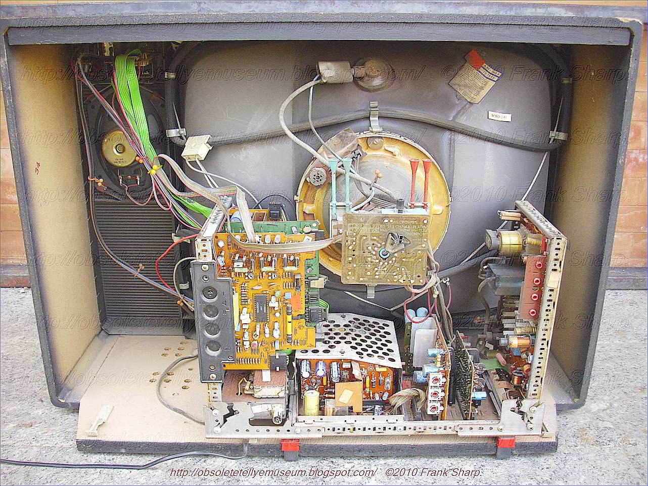


This Line of CGE TELEFUNKEN television set was called the kronosystem and was introducing the TELEFUNKEN CHASSIS 714A with the already introduced 30AX CRT TUBE one year earlyer on chassis TELEFUNKEN 714, this was the last "OPEN BOOK" chassis design type technology with his unique modularity (see pictures) and with some add on capability never officially marketed because TELEFUNKEN in 1981 ceased to produce tellyes in this way.
The 714A Is introducing the use of the TDA3560 as PAL MonoChip for chroma-luminance section, to integrate in one unit Video and RGB stages.
This version here shown was introducing the PLL BS 2 BS653 UNIT featuring the use of 2 NATIONAL COP400 CONTROL PROCESSORS in TELEVISION PLL SYNTHESIZER TUNING.
The successor chassis type was the CHASSIS 415 and related types.
LAST TELEFUNKEN CHASSIS DEVELOPED IN THIS WAY FOREVER !!!!!!!!


CGE (TELEFUNKEN) CT6290 TV26" TELECOLOR KRONOSYSTEM CHASSIS 714A PLL 2 Frequency synthesizer tuning system for television receivers:
SHOWING COP421 + COP420 + MM5439 IN BS653 PLL2 UNIT:

" A method for tuning a television receiver having automatic frequency control to the carrier frequency of a selected broadcast channel with an associated channel number including generating a variable frequency signal by means of a local oscillator, generating a reference frequency signal by means of a reference oscillator, and generating a local oscillator correction signal for matching an intermediate frequency signal derived from said local oscillator signal and the carrier frequency signal with a predetermined nominal intermediate frequency signal, said method being characterized by the use of a microcomputer and comprising:
generating binary signals representing first and second digital tune words, said digital tune words representing a selected channel;
storing said first and second digital tune words in a first data memory in said microcomputer;
reading said first and second digital tune words from said first memory and generating a divided-down local oscillator frequency by the use of said first digital tune word and a divided-down reference oscillator frequency by the use of said second digital tune word;
comparing said divided-down local oscillator and reference frequencies and generating a control signal representative of the difference in frequency of said divided-down local oscillator and reference frequencies;
coupling said control signal to said local oscillator for causing it to be locked to the frequency of said received carrier signal;
mixing the local oscillator frequency signal and the carrier frequency signal to generate an intermediate frequency signal;
comparing said intermediate frequency signal with said predetermined nominal intermediate frequency signal and providing a tuning voltage to said microcomputer, said tuning voltage being indicative of the magnitude and direction of a tuning error between said intermediate frequency signal and said predetermined nominal intermediate frequency signal;
incrementally adjusting the reference oscillator frequency by means of a tuning signal provided to said reference oscillator by said microcomputer in response to said tuning voltage;
detecting when the incrementally changing, divided-down reference oscillator frequency causes the intermediate frequency signal to pass said predetermined nominal intermediate frequency signal; and
incrementally stepping the divided-down reference oscillator frequency back a predetermined number of steps following the passage of said predetermined nominal intermediate frequency signal by said intermediate frequency signal in tuning said television receiver to the selected channel.
"
 A television tuning system employs a frequency synthesizer system for establishing the tuning of the receiver. A programmable frequency divider counter is connected between the output of a reference oscillator and a phase comparator to which the output of the local oscillator in the tuner also is applied. The phase comparator output provides a tuning voltage for controlling the tuning of the local oscillator. A microprocessor is used to control the count of the programmable frequency divider and initially to set a count corresponding to the selected channel in a counter connected between the output of the local oscillator and the phase comparator. The tuning consists of three discrete time periods. First, a settling time to allow channel change transients to settle; second, a short period of forced search at a relatively rapid rate to insure proper tuning; and third, a slower rate of step-by-step correction to accomodate for station drift and the like during reception. This third time period is initiated either by the passage of a fixed length of time following the start of the forced search period or by sensing a preestablished number of changes of state in the output of the frequency discriminator during the forced/search period.
1. A tuning system for the tuner of a television receiver capable of receiving a composite television signal and including frequency discriminator (AFT) circuit means, said system including in combination:
a reference oscillator providing a reference signal at a predetermined frequency;
a local oscillator in the tuner providing a variable output frequency in response to the application of a control signal thereto;
a programmable frequency divider means having first and second inputs coupled respectively to the output of said reference oscillator and said local oscillator for producing signals on first and second outputs having frequencies which are a programmable fraction of the frequency of the signals applied to the inputs thereto;
phase comparator means having one input coupled with the first output of said programmable frequency divider means and having another input coupled with the second output of said programmable frequency divider means for developing a control signal and applying such control signal to said local oscillator for controlling the output frequency thereof;
counter circuit means coupled with said programmable frequency divider means for initially setting said divider means to a predetermined division ratio and operating to change the programmable fraction of division thereof in accordance with changes in the count in said counter circuit means;
control circuit means coupled with the output of said frequency discriminator means and further coupled with said counter circuit means for causing said counter circuit means to count at a first rate in a predetermined direction determined by the state of the output signal from said discriminator means in the absence of a predetermined signal output from said frequency discriminator means until a predetermined maximum count is attained, thereupon resetting said counter circuit means to a count which is a predetermined amount less than said maximum predetermined count and continuing to count at said first rate in the same predetermined direction from said new count to continuously change the programmable fraction of said frequency divider means in accordance with the state of operation of said counter circuit means, said control means operating in response to said predetermined signal output from the frequency discriminator means for terminating operation of said counter circuit means; and
further means for terminating operation of said counter circuit means at said first rate and causing operation thereof at a second slower rate.
2. The combination according to claim 1 wherein said further means includes timing means initiated into operation simultaneously with the setting of said divider means to a predetermined division ratio, and after a predetermined time interval said timing means producing an output signal applied to said counter circuit means to cause operation thereof to take place at said second slower rate. 3. The combination according to claim 1 wherein said counter circuit means includes a reversible digital counter coupled with said programmable frequency divider, means and said control circuit means causes said counter circuit means to count in said predetermined direction when the output of said frequency discriminator is of a first state and to count in the opposite direction when the output of said frequency discriminator is of second state; and said further means comprises means coupled with the output of said frequency discriminator and with said counter circuit means to take place at said second slower rate in response to a predetermined number of changes of state of frequency discriminator. 4. The combination according to claim 3 further including means responsive to the selection of a new channel in said television receiver for resetting said further means to an initial condition of operation. 5. The combination according to claim 4 wherein said further means comprises a search termination counter means operative to provide an output signal applied to said counter circuit means in response to a count thereby of a predetermined number of changes of state of said frequency discriminator to cause said counter circuit means to be operated at said second slower rate.
TELEFUNKEN CHASSIS 714A (AT349354097) Switching power supply, especially for a T.V. receiving apparatus:
 1. Switch mode power supply means, especially for a television receiver,
having a working winding (5), a switching transistor (6), a
back-coupling winding (7) and a control switch (11) on the primary side
of a divided transformer (1), and also having rectifiers (15, 16, 20)
for the production of the drive voltages (U1, U2, U3) on the secondary
side of the transformer (1), characterized by the following features :
(a) Connected to a winding (19) there is a thyristor (24) which is poled
in the permitted direction for the voltage at the winding (19) arising
during the current conducting phase of the switching transistor (6). (b)
One of the drive voltages (U2) is applied to the control electrode of
the thyristor (24) with such magnitude that the thyristor (24) remains
blocked in the normal working state and fires on the occurrence of an
inadmissible rise of the drive voltage (U3).
1. Switch mode power supply means, especially for a television receiver,
having a working winding (5), a switching transistor (6), a
back-coupling winding (7) and a control switch (11) on the primary side
of a divided transformer (1), and also having rectifiers (15, 16, 20)
for the production of the drive voltages (U1, U2, U3) on the secondary
side of the transformer (1), characterized by the following features :
(a) Connected to a winding (19) there is a thyristor (24) which is poled
in the permitted direction for the voltage at the winding (19) arising
during the current conducting phase of the switching transistor (6). (b)
One of the drive voltages (U2) is applied to the control electrode of
the thyristor (24) with such magnitude that the thyristor (24) remains
blocked in the normal working state and fires on the occurrence of an
inadmissible rise of the drive voltage (U3).
TELEFUNKEN PALCOLOR CHASSIS 714A Schaltnetzteil AT349354097
(AT 349354097), IN GERMAN:
1. Schaltnetzteil,
insbesondere f·ur einen Fernsehempf·anger, mit einer Arbeitswicklung
(5), einem Schalttransistor (6), einer R·uckkopplungswicklung (7) und
einer Regelschaltung (ii) auf der Prim·arseite sowie mit Gleichrichtern
(15,16, 20) zur Erzeugung von Betriebsspannungen (U11U2#U3) auf der
Sekund·arseite eines Trenntransformators (1) gekenn zeichnet durch
folgende Merkmale: a) An eine Wicklung (19) ist ein Thyristor (24)
angeschlos sen, der f·ur die w·ahrend der siromf·uhrenden Phase der
Schalttransistoren (6) an der Wicklung (19) auftreten de Spannung in
Durchlassrichtung gepolt ist. b) An die Steuerelektrode des Thyristors
(24) ist eine der Betriebsspannungen (U2) in solcher H·ohe angelegt,
dass der Thyristor (24) im Normalbetrieb gesperrt bleibt und bei einem
unzul·assigen Anstieg der Betriebs spannung (U3) z·undet.

2. Netzteil nach Anspruch 1, dadurch gekennzeichnet, dass die Betriebsspannung (U3) ·uber einen Spannungsteiler (25,26) an die Steuerelektrode des Thyristors (24) angelegt ist.
3. Netzteil nach Anspruch 1, dadurch gekennzeichnet, dass die Wicklung (19) eine Sekund·arwicklung des Trenntransforma tors (1) ist.
TELEFUNKEN CHASSIS 714A Switching Power supply voltage stabilizer:
A power supply voltage stabilizer comprising a transformer, of which the primary winding is connected to a switching means for controlling power supply to the primary winding. An oscillator circuit is associated with the switching means in order to control on/off operation of the switching means. An abnormal overvoltage and/or overcurrent detection circuit is provided for terminating the oscillation operation of the oscillator circuit when impending overvoltage and/or overcurrent is detected.
1. A power supply voltage stabilizer comprising:
a transformer including a primary winding connected to a power source and a secondary winding for output purposes;
switching means connected to said primary winding for controlling power supply to sai
 d primary winding;
an oscillator circuit for controlling on/off operation of said switching means; and
abnormal condition detection means for developing a control signal for terminating oscillation operation of said oscillator circuit when an abnormal condition is detected;
said oscillator circuit including an astable multivibrator, and variable impedance means for varying an oscillation frequency of said astable multivibrator.
2. A power supply voltage stabilizer comprising:
a transformer including a primary winding connected to a power source and a secondary winding for output purposes;
switching means connected to said primary winding for controlling power supply to said primary winding;
an oscillator circuit for controlling on/off operation of said switching means; and
abnormal condition detection means for developing a control signal for terminating oscillation operation of said oscillator circuit when an abnormal condition is detected;
said transformer further including an auxiliary winding for developing a voltage proportional to that developed through said secondary winding, said voltage developed through said auxiliary winding being applied to said oscillator circuit for driving said oscillator circuit;
said abnormal condition detection means including an overvoltage detection circuit connected to said auxiliary winding for developing said control signal when an overvoltage is developed through said auxilliary winding;
said oscillator circuit comprising an astable multivibrator, and variable impedance means for varying an oscillation frequency of said astable multivibrator.
3. A power supply voltage stabilizer comprising:
a transformer including a primary winding connected to a power source and a secondary winding for output purposes;
switchi
ng means connected to said primary winding for controlling power supply to said primary winding;
an oscillator circuit for controlling on/off operation of said switching means; and
abnormal condition detection means for developing a control signal for terminating oscillation operation of said oscillator circuit when an abnormal condition is detected;
said transformer further including an auxiliary winding for developing a voltage proportional to that developed through said secondary winding, said voltage developed through said auxiliary winding being applied to said oscillator circuit for driving said oscillator circuit;
said abnormal condition detec
 tion means including an overvoltage detection circuit connected to said auxiliary winding for developing said control signal when an overvoltage is developed through said auxiliary winding;
said overvoltage detection circuit including a latching means for continuously developing said control signal.
4. A power supply voltage stabilizer comprising:
a transformer including a primary winding connected to a power source and a secondary winding for output purposes;
switching means connected to said primary winding for controlling power supply to said primary winding;
an oscillator circuit for controlling on/off operation of said switching means;
abnormal condition detection means for developing a control signal for terminating oscillation operation of said oscillator circuit when an abnormal condition is detected;
said transformer further including an auxiliary winding for developing a voltage proportional to that developed through said secondary winding, said voltage developed through said auxiliary winding being applied to said oscillator circuit for driving said oscillator circuit;
said abnormal condition detection means including an overvoltage detection circuit connected to said auxiliary winding for developing said control signal when an overvoltage is developed through said auxiliary winding;
said overvoltage detection circui t further includes,
a reference voltage generation means for developing a reference voltage proportional to a voltage applied from said power source; and
comparing means for comparing said voltage developed through said auxiliary winding with said reference voltage in order to develop said control signal when said voltage developed through said auxiliary winding exceeds said reference voltage.
5. A power supply voltage stabilizer comprising:
a transformer including a primary winding connected to a power source and a secondary winding for output purposes;
switching means connected to said primary winding for controlling power supply to said primary winding;
an oscillator circuit for controlling on/off operation of said switching means; and
abnormal condition detection means for developing a control signal for terminating oscillation operation of said oscillator circuit when an abnormal condition is detected;
said abnormal condition detection means including an overcurrent detection circuit connected to said primary winding for developing said control signal when an overcurrent flows through said primary winding;
wherein said oscillator circuit includes an astable multivibrator, and variable impedance means for varying an oscillation frequency of said astable multivibrator.
6. A power supply voltage stabilizer comprising:
a transformer including a primary winding connected to a power source and a secondary winding for output purposes;
switching means connected to said primary winding for controlling power supply to said primary winding;
an oscillator circuit for controlling on/off operation of said switching means; and
abnormal condition detection means for developing a control signal for terminating oscillation operation of said oscillator circuit when an abnormal condition is detected;
said abnormal condition detection means including an overcurrent detection circuit connected to said primary winding for developing said control signal when an overcurrent flows through said primary winding;
said overcurrent detection circuit including a latching means for continuously developing said control signal;
said oscillator circuit including an astable multivibrator, and variable impedance means for varying an oscillation frequency of said astable multivibrator.
7. The power supply voltage stabilizer of claim 1, 2, 5, or 6, wherein said variable impedance means comprise a photo transistor, and wherein a light emitting diode is connected to said secondary wind ing for emitting a light of which amount is proportional to a voltage developed through said secondary winding, said light emitted from said light emitting diode being applied to said photo transistor. 8. The power supply voltage stabilizer of claim 7, wherein said light emitting diode and said photo transistor are incorporated in a single photo coupler. 9. A power supply voltage stabilizer comprising:
a transformer including a primary winding connected to a power source and a secondary winding for output purposes;
switching means connected to said primary winding for controlling power supply to said primary winding;
an oscillator circuit for controlling on/off operation of said switching means; and
abnormal condition detection means for developing a control signal for terminating oscillation operation of said oscillator circuit when an abnormal condition is detected;
said transformer further including an auxiliary winding for developing a voltage proportional to that developed through said secondary winding, said voltage developed through said auxiliary winding being applied to said oscillator circuit for driving said oscillator circuit;
said abnormal condition detection means including an overvoltage detection circuit connected to said auxiliary winding for developing said control signal when an overvoltage is developed through said auxilliary winding;
said overvoltage detection circuit including a latching means for continuously developing said control signal;
said oscillator circuit including an astable multivibrator, and variable impedance means for varying an oscillation frequency of said astable multivibrator.
10. A power supply voltage stabilizer comprising:
a transformer including a primary winding connected to a power source and a secondary winding for output purposes;
switching means connected to said primary winding for controlling power supply to said primary winding;
an oscillator circuit for controlling on/off operation of said switching means;
abnormal condition detection means for developing a control signal for terminating oscillation operation of said oscillator circuit when an abnormal condition is detected;
said transformer further including an auxiliary winding for developing a voltage proportional to that developed th rough said secondary winding, said voltage developed through said auxiliary winding being applied to said oscillator circuit for driving said oscillator circuit;
said abnormal condition detection means including an overvoltage detection circuit connected to said auxiliary winding for developing said control signal when an overvoltage is developed through said auxiliary winding;
said overvoltage detection circuit including,
a reference voltage generation means for developing a reference voltage proportional to a voltage applied from said power source; and
comparing means for comparing said voltage developed through said auxiliary winding with said reference voltage in order to develop said control signal when said voltage developed through said auxiliary winding exceeds said reference voltage;
said oscillator circuit including an astable multivibrator, and a variable impedance means for varying an oscillation frequency of said astable multivibrator.
11. A power supply voltage stabilizer comprising:
transformer means including a primary winding connected to a power source, a secondary winding for producing an output voltage, and an auxiliary winding for developing a voltage proportional to said output voltage produced by said secondary winding;
switching means connected to said primary winding for controlling the power supply from said power source to said primary winding;
oscillator circuit means for controlling the on/off operation of said switching means;
overvoltage detection circuit means connected to said auxiliary winding for developing a control signal to terminate the oscillation operation of said oscillator circuit means when an overvoltage condition is detected, said overvoltage detection circuit means including,
means for developing a reference potential, and
comparing means responsive to said voltage developed at said auxiliary winding and to said reference potential for comparing said reference potential with said voltage developed at said auxiliary winding and for generating said control signal to terminate the oscillation operation of said oscillator circuit means when said voltage developed at said auxiliary winding exceeds said reference potential.
12. A power supply voltage stabilizer comprising:
transformer means including a primary winding connected to a power source and having a voltage supplied thereto, a secondary winding for producing an output voltage, and an auxiliary winding for developing a voltage proportional to said output voltage produced by said secondary winding;
switching means connected to said primary winding for controlling the power supply from said power source to said primary winding;
oscillator circuit means for controlling the on/off operation of said switching means;
overcurrent detection circuit means connected to said primary winding for developing a control signal to terminate the oscillation operation of said oscillator circuit means when an overcurrent condition is detected, said overcurrent detection circuit means including,
means for monitoring said voltage supplied to said primary winding of said transformer means,
means for measuring the amount of current passing through said primary winding of said transformer means by translating said amount of current into a corresponding amount of voltage potential,
switching means responsive to said corresponding amount of voltage potential for switching to a first switched condition when the corresponding voltage potential exceeds a predetermined voltage potential and for switching to a second switched condition when said voltage potential does not exceed said predetermined voltage potential, and
comparing means responsive to said voltage supplied to said primary winding and connected to an output of said switching means for generating said control signal to terminate oscillation operation of said oscillator circuit means when said switching means switches to said first switched condition in response to the exceeding of said predetermined voltage potential by said corresponding voltage potential.
13. A power supply voltage stabilizer in accordance with claim 11 or 12 wherein said comparing means comprises a double base diode.
The present invention relates to a power supply voltage stabilizer and, more particularly, to a power supply voltage stabilizer employing a switching system for controlling power supply to a transformer included in the power supply voltage stabilizer.
In the conventional power supply voltage stabilizer employing a switching system for controlling power supply to a transformer included in the power supply voltage stabilizer, there is a possibility that an abnormal overvoltage will be developed from an output terminal thereof and/or an abnormal overcurrent may flow through the primary winding of the transformer.
Accordingly, an object of the present invention is to provide a protection means for protecting the power supply voltage stabilizer from an abnormal overvoltage and/or overcurrent.
Another object of the present invention is to provide a detection means for detecting an impending overvoltage and/or overcurrent occurring within the power supply voltage stabilizer.
Other objects and further scope of applicability of the present invention will become apparent from the detailed description given hereinafter. It should be understood, however, that the detailed description and specific examples, while indicating preferred embodiments of the invention, are given by way of illustration only, since various changes and modifications within the spirit and scope of the invention will become apparent to those skilled in the art from this detailed description.
The
 power supply voltage stabilizer of the present invention mainly comprises a transformer including a primary winding connected to a commercial power source through a rectifying circuit, a secondary winding for output purposes, and an auxiliary winding. A driver circuit including a switching means is connected to the primary winding for controlling the power supply to the primary winding. An oscillator circuit is associated with the switching means to control ON/OFF operation of the switching means, thereby controlling the power supply to the primary winding.
To achieve the above objects, pursuant to an embodiment of the present invention, an overvoltage detection circuit is connected to the auxiliary winding. The overvoltage detection circuit functions to compare a voltage created in the auxiliary winding with the rectified power supply voltage, and develop a control signal, when an impending overvoltage is detected, for terminating operation of the oscillator circuit, thereby precluding power supply to the primary winding.
In another embodiment of the present invention, an overcurrent detection circuit is provided for detecting an impending overcurrent flowing through the primary winding to develop a control signal for terminating operation of the oscillator circuit.
BRIEF DESCRIPTION OF THE DRAWINGS
The present invention will become more fully understood from the detailed description given hereinbelow and the accompanying drawings, which are given by way of illustration only, and thus are not limitative of the present invention and wherein:
FIG. 1 is a circuit diagram of a basic construction of a power supply voltage stabilizer of the present invention;
FIG. 2 is a block diagram of an embodiment of a power supply voltage stabilizer of the present invention, which includes an oscillator circuit and an over voltage detection circuit;
FIG. 3 is a circuit diagram of an embodiment of the overvoltage detection circuit included in the power supply voltage stabilizer of FIG. 2;
FIG. 4 is a circuit diagram of an embodiment of the oscillator circuit included in the power supply voltage stabilizer of FIG. 2;
FIG. 5 is a waveform chart for explaining operation of the oscillator circuit of FIG. 4;
FIG. 6 is a block diagram of another embodiment of a power supply voltage stabilizer of the present invention, which includes an oscillator circuit and an overcurrent detection circuit; and
FIG. 7 is a circuit diagram of an embodiment of the overcurrent detection circuit included in the power supply voltage stabilizer of FIG. 6.
DESCRIPTION OF THE PREFERRED EMBODIMENTS
R eferring now in detail to the drawings, and to facilitate a more complete understanding of the present invention, a basic construction of a power supply voltage stabilizer of the present invention will be first described with reference to FIG. 1.
The power supply voltage stabillizer mainly comprises a transformer T including a primary winding N 1 connected to a commercial power source V, a secondary winding N 2 connected to an output terminal V 0 , and an auxiliary winding N 3 . An oscillator circuit OSC is associated with the primary winding N 1 and the auxiliary winding N 3 to control the power supply from the commercial power source V to the primary winding N 1 .
A rectifying circuit E is connected to the commercial power source V for applying a rectified voltage to a capacitor C 1 . A negative terminal of the capacitor C 1 is grounded, and a positive terminal of the capacitor C 1 is connected to the collector electrode of a switching transistor Q 5 through the primary winding N 1 of the transformer T. The oscillator circuit OSC performs the oscillating operation when receiving a predetermined voltage, and develops a control signal toward the base electrode of the switching transistor Q 5 to control the switching operation of the switching transistor Q 5 . The switching transistor Q 5 functions to control the power supply to the primary winding N 1 , thereby controlling the power transfer to the secondary winding N 2 and the auxiliary winding N 3 .
The auxiliary winding N 3 is connected to a capacitor C 3 in a parallel fashion via a diode D 1 . A positive terminal of the capacitor C 3 is connected to the oscillator circuit OSC to supply a drive voltage Vc 3 . A negative terminal of the capacitor C 3 is connected to the emitter electrode of the switching transistor Q 5 and grounded. The positive terminal of the capacitor C 3 is connected to the primary winding N 1 via a diode D 2 and a capacitor C 2 in order to stabilize the initial condition of the oscillator circuit OSC.
The secondary winding N 2 functions to develop a predetermined voltage through the output terminal V 0 . A smoothing capacitor C 0 is connected to the secondary winding N 2 via a diode D 0 , and a series circuit of a resistor R 0 and a light emitting diode D i is connected to the smoothing capacitor C 0 in a parallel fashion. The light emitted from the light emitting diode D i is applied to a photo transistor Q 8 employed in the oscillator circuit OSC. The light emitting diode D i and the photo transistor Q 8 are preferably incorporated in a single package as a photo coupler.
The light amount emitted from the light emitting diode D i is proportional to the output voltage developed from the output terminal V 0 . The photo transistor Q 8 exhibits the impedance corresponding to the applied light amount. The oscillator circuit OSC is so constructed that the oscillation frequency is varied in response to variation of the impedance of the photo transistor Q 8 . Accordingly, the ON/OFF operation of the switching transistor Q 5 is controlled in response to the output voltage level, thereby stabilizing the output voltage level.
In the above constructed power supply voltage stabilizer, there is a possibility that an abnormal overvoltage is developed through the secondary winding N 2 and the auxiliary winding N 3 when the oscillator circuit OSC or the light emitting diode D i is placed in the fault condition.
FIG. 2 show s an embodiment of the power supply voltage stabilizer of the present invention, which includes means for precluding occurrence of the above-mentioned overvoltage. Like elements corresponding to those of FIG. 1 are indicated by like numerals.
The power supply voltage stabilizer of FIG. 2 mainly comprises the transformer T, the oscillator circuit OSC, a driver circuit 1 including the switching transistor Q 5 , and an overvoltage detection circuit 3.
The positive terminal of the capacitor C 3 is connected to the driver circuit 1 and the oscillator circuit OSC to apply the driving voltage thereto. The positive terminal of the capacitor C 3 is also connected to the primary winding N 1 through the diode D 2 and a parallel circuit of the capacitor C 2 and a resistor R 2 in order to stabilize the initial start operation of the oscillator circuit OSC. The secondary winding N 2 is connected to an output level detector 2, which comprises the light emitting diode D i as shown in FIG. 1. The ON/OFF control of the switching transistor Q 5 is similar to that is achieved in the power supply voltage stabilizer of FIG. 1.
The secondary winding N 2 and the auxiliary winding N 3 are wound in the same polarity fashion and, therefore, the voltage generated through the auxiliary winding N 3 is proportional to that voltage generated through the secondary winding N 2 . The overvoltage detection circuit 3 is connected to receive the voltage at a point a as a power source voltage, and the voltage at a point b which is connected to the positive terminal of the capacitor C 3 . When the voltage level at the point b exceeds a reference level, the overvoltage detection circuit 3 develops a control signal for terminating the operation of the oscillator circuit OSC.
FIG. 3 shows a typical construction of the overvoltage detection circuit 3.
The voltage at the point a is applied to a series circuit of resistors R 3 and R 4 , and grounded. The voltage at the point b is applied to the connection point of the resistors R 3 and R 4 via a diode D 3 . The connection point of the resistors R 3 and R 4 is grounded through resistors R 5 and R 6 and a Zener diode Z 1 . A double-base diode (Trade Name Programmable Unijunction Transistor) P 1 is provided for developing the control signal to be applied to the oscillator circuit OSC. The anode electrode of the programmable unijunction transistor P 1 is connected to the connection point of the resistors R 3 and R 4 , the gate electrode of the programmable unijunction transistor P 1 is connected to the connection point of the resistors R 5 and R 6 , and the cathode electrode is connected to the oscillator circuit OSC.
When the voltage level of the point b exceeds a reference level VZ 1 , the programmable unijunction transistor P 1 is turned on to develop the control signal for terminating the oscillation operation of the oscillator OSC. In this way, the impending abnormal overvoltage is detected to protect the circuit elements. The ON condition of the programmable unijunction transistor P 1 is maintained as long as the main power switch is closed, because the overvoltage detection circuit 3 is connected to receive the voltage from the point a.
The voltage detection circuit 3 does not necessarily employ the programmable unijunction transistor. Another element showing the latching characteristics such as a negative resistance element can be employed instead of the programmable unijunction transistor.
FIG. 4 shows a typical construction of the oscillator circuit OSC.
The oscillation circuit OSC mainly comprises an astable multivibrator including transistors Q 1 , Q 2 and Q 3 , and an output stage including a transistor Q 4 . The astable multivibrator is connected to receive the voltage appearing across the capacitor C 3 , and develops an output signal of which frequency is determined by the circuit condition as long as the multivibrator receives a voltage greater than a predetermined level.
The output signal of the output stage is applied to the base electrode of the switching transistor Q 5 included in the driver circuit 1 in order to switch the switching transistor Q 5 with a predetermined frequency. A transistor Q 9 is interposed between the base electrode of the transistor Q 3 and the grounded terminal. The transistor Q 9 is controlled by the control signal derived from the overvoltage detection circuit 3. Accordingly, the transistor Q 3 is turned off to terminate the oscillation operation when the abnormal overvoltage is detected by the overvoltage detection circuit 3.
Now assume that a voltage Vc 3 is developed across the capacitor C 3 . When main power supply switch is closed, the voltage Vc 3 varies in a manner shown by a curve X in FIG. 5. When the voltage Vc 3 reaches a predetermined level, the astable multivibrator begins the oscillation operation. More specifically, the transistor Q 1 is first turned on because the base electrode of the transistor Q 1 is connected to a capacitor C 4 of which the capacitance value is relatively small. At this moment, the transistor Q 2 is held off.
Because of turning on of the transistor Q 1 , the capacitor C 4 is gradually charged through a resistor R 4 and the transistor Q 1 . Accordingly, the base electrode voltage of the transistor Q 1 is gradually increased and, hence, the emitter electrode voltage of the transistor Q 1 is also increased to turn on the transistor Q 2 . When the transistor Q 2 is turned on, the transistor Q 3 is also turned on. The base electrode voltage of the transistor Q 2 which is bypassed by a resistor R 1 is reduced and, therefore, the transistor Q 2 is stably on. At this moment, the transistor Q 1 is turned off.
When the transistor Q 3 is turned on, the transistor Q 4 is turned on to develop a signal to turn on the switching transistor Q 5 . Upon turning on of the transistor Q 3 , the charge stored in the capacitor C 4 is gradually discharged through paths shown by arrows in FIG. 4. Therefore, the base electrode voltage of the transistor Q 1 is gradually reduced. When the base electrode voltage of the transistor Q 1 becomes less than a predetermined level, the transistor Q 1 is turned on, and the transistor Q 2 , Q 3 and Q 4 are turned off. Accordingly, the transistor Q 5 is turned off. After passing the initial start condition, the driving voltage Vc 3 is held at a predetermined level as shown by a curve Y in FIG. 5 to maintain the above-mentioned oscillation operation.
The photo transistor Q 8 is disposed in the discharge path of the capacitor C 4 in order to control the discharge period in response to the impedance of the photo transistor Q 8 . That is, the oscillation frequency is controlled in response to the light amount emitted from the light emitting diode included in the output level detector 2.
FIG. 6 shows another em bodiment of the power supply voltage stabilizer of the present invention, which includes means for precluding occurrence of an abnormal overcurrent. Like elements corresponding to those of FIG. 2 are indicated by like numerals.
In the power supply voltage stabilizer of FIG. 1, there is a possibility that an abnormally large current flows through the primary winding N 1 when the magnetic flux is saturated due to requirement of large current at the secondary winding side. The power supply voltage stabilizer of FIG. 6 includes an overcurrent detection circuit 4 for detecting an impending abnormally large current.
A resistor R 9 is interposed between the emitter electrode of the switching transistor Q 5 included in the driver circuit 1 and the grounded terminal. The overcurrent detection circuit 4 is connected to receive a signal from the connection point of the resistor R 9 and the emitter electrode of the switching transistor Q 5 , thereby developing a control signal for terminating the oscillation operation of the oscillation circuit OSC.
FIG. 7 shows a typical construction of the overcurrent detection circuit 4.
The voltage at the point a is applied to a series circuit of resistors R 10 and R 11 , and grounded. The collector electrode of a transistor Q 10 is connected to the connection point of the resistors R 10 and R 11 through resistors R 12 and R 13 . The emitter electrode of the transistor Q 10 is grounded. The base electrode of the transistor Q 10 is connected to the connection point of the resistor R 9 and the emitter electrode of the switching transistor Q 5 via a resistor R 14 .
When the switching transistor Q 5 is turned on, a current flows through the resistor R 9 . When the voltage drop across the resistor R 9 exceeds a predetermined value due to a large current, the transistor Q 10 is turned on to turn on the programmable unijunction transistor P 1 . That is, when a large current flows through the primary winding N 1 , the programmable unijunction transistor P 1 develops the control signal to terminate the oscillation operation of the oscillator circuit OSC.
The invention being thus described, it will be obvious that the same may be varied in many ways. Such variations are not to be regarded as a departure from the spirit and scope of the invention, and all such modifications are intended to be included within the scope of the following claims.
TELEFUNKEN CHASSIS 714A AMBIENT LIGHT RESPONSIVE CONTROL OF BRIGHTNESS, CONTRAST AND COLOR SATURATION
 1. In a color television apparatus, a circuit for varying color display characteristics in accordance with variations in ambient light comprising: 2. In a color picture display system having a display device comprising: 3. The display system of claim 2 with kinescope means having a first set of electrodes and a second set of electrodes, 4. The display system of claim 2 with said light sensing means being responsive to the intensity of the ambient light and said parameter varying in accordance with the intensity of ambient light. 5. The display system of claim 4 with said modifying means increasing the gain of said luminance amplifying means at a greater rate than the gain of said chroma amplifying means as said ambient light intensity is increased. 6. A color television apparatus comprising: 7. In a color television receiver: 8. The receiver of claim 7 with said modifying means comprising a light dependent resistor means, 9. The receiver of claim 8 with second impedance means coupling said light dependent resistor means to said luminance gain means to control the gain of said luminance gain means. 10. The receiver of claim 9 with said second impedance means comprising a parallel combination of capacitance and resistance. 11. The receiver of claim 7 with said modifying means varying the gain of the luminance gain means at a greater rate than the gain of the chroma gain means as ambient light is varied. 12. The receiver of claim 7 with said modifying means being responsive to the intensity of ambient light and said parameter being varied as the intensity of the ambient light is varied. 13. The receiver of claim 7 with said modifying means attenuating the gain of said luminance amplifying means approximately fifty percent more than the gain of said chroma amplifying means, when the attenuation is measured in decibels, as said ambient light intensity is decreased. 14. In a color television receiver:
TELEFUNKEN CHASSIS 714A AMBIENT LIGHT RESPONSIVE CONTROL OF BRIGHTNESS, CONTRAST AND COLOR SATURATION Gain control arrangement useful in a television signal processing systemIn a color television receiver, first and second amplifiers are respectively included in the luminance and chrominance channels to permit control of contrast and saturation. The amplifiers have gain versus contr ol voltage characteristics including linear portions extrapolated to cut off at predetermined voltages which may or may not be the same. A first potentiometer is coupled between a source of fixed voltage equal to the extrapolated cut off voltage of the first amplifier and a gain controlling voltage source. The gain controlling voltage may be produced by a circuit including an element responsive to ambient light. The wiper of the first potentiometer is coupled to the first amplifier to couple a voltage developed at a predetermined point of the first potentiometer to the first amplifier to control its gain. A second potentiometer is coupled between a source of voltage equal to the extrapolated cut off voltage of the second amplifier and the gain controlling voltage source to receive a portion of the gain controlling voltage in accordance with the ratio of the extrapolated cut off voltages of the first and second amplifiers. The wiper of the second potentiometer is coupled to the second amplifier to couple a voltage developed at a predetermined point of the second potentiometer to the second amplifier to control its gain. In this manner, the contrast of the receiver may be varied over a relatively wide range while saturation is maintained substantially constant.
1. In a color television signal processing system of the type including luminance and chrominance signal processing channels, apparatus comprising:
first and second amplifiers respectively included in said luminance and chrominance channels, said amplifiers having gain versus control voltage characteristics including linear portions extrapolated to cut-off at predetermined voltages which may or may not be the same voltage;
a gain controlling voltage source;
means for coupling said gain controlling voltage to said first amplifier to control its gain;
potentiometer means coupled between a fixed voltage substantially equal to the extrapolated cut-off voltage of said second amplifier and to said gain controlling voltage source to recieve a portion of said gain controlling voltage in accordance with the ratio of the extrapolated cut-off voltages of said first and second amplifiers; and
means for coupling a voltage developed at a predetermined point on said potentiometer means to said second amplifier to control its gain.
2. The apparatus recited in claim 1 wherein said means for coupling said gain controlling voltage to said first amplifier includes another potentiometer coupled between a source of fixed voltage substantially equal to the extrapolated cut-off voltage of said first amplifier and said gain controlling voltage source. 3. In a color television signal processing system of the type including luminance and chrominance signal processing channels, apparatus comprising:
first and second amplifiers respectively included in said luminance and chrominance channels, said amplifiers having gain control voltage characteristics including linear portions extrapolated to cut-off at substantially the same predetermined voltage;
a source of gain controlling voltage; and
means for coupling said gain controlling voltage to said first and second amplifiers.
4
 . Apparatus comprising:
first variable gain amplifying means for amplifying a first signal in response to a first DC control signal, said first amplifying means having a first gain versus DC control voltage characteristic including a linear region, said linear region having a gain substantially equal to 0 at a DC control voltage equal to VO ;
second variable gain amplifying means for amplifying a second signal in response to a second DC control signal, said second amplifying means having a second gain versus DC control voltage characteristic including a linear region, said linear region having a gain substantially equal to 0 at a DC control voltage equal to AVO, where A is a number greater than 0;
a first source of fixed voltage substantially equal to VO ;
a second source of fixed voltage substantially equal to AVO ;
means for developing a third DC control voltage v;
means for developing a portion Av of said third control voltage v;
first means for deriving said first control voltage including means for providing the difference between said third control voltage v and said fixed voltage VO and means for adding a predetermined portion of the difference between said third control voltage v and said fixed voltage VO to said DC control voltage v; and
second means for deriving said second control voltage including means for providing the difference between a portion Av of said third control voltage v and said fixed voltage AVO and means for adding a predetermined portion of the difference between said portion Av and said fixed voltage AVO to said DC control voltage v.
5. The apparatus recited in claim 4 wherein A is equal to 1 . 6. The apparatus recited in claim 4 wherein said first amplifying means is included in a luminance channel of a televeision signal processing system and said second amplifying means is included in a chrominance channel of said television signal processing system. 7. The apparatus recited in claim 6 wherein means for developing said third control voltage includes means responsive to ambient light. 8. The apparatus recited in claim 4 wherein said first means includes first voltage divider means coupled between said fixed voltage VO and said third DC control voltage v; and wherein said second means includes second voltage divider means coupled between said fixed voltage AVO and said portion Av. 9. The apparatus recited in claim 8 wherein said first voltage divider means includes a first potentiometer, said first potentiometer having a wiper coupled to said first amplifying means; and wherein said second voltage divider means includes a second potentiometer, said second potentiometer having a wiper coupled to said amplifying means. 10. The apparatus recited in claim 4 wherein said second gain versus DC control voltage characteristic includes a region between said voltage AVO and a voltage VB where the gain is greater than 0, said voltage VB being substantially equal to the voltage at which said second amplifying means has a gain substantially equal to 0; and wherein said second source of fixed voltage includes means for coupling said voltage VB to said second amplifying means. 11. The apparatus recited in claim 10 wherein said second source of said voltage AVO includes a third source of fixed voltage VB ; potentiometer means coupled between said third source of fixed voltage VB and said means for developing said third DC control voltage; and means coupled to said potentiometer means for developing said voltage AVO at a point along said potentiometer means; said potentiometer means including a wiper coupled to said second amplifier means, said wiper being adjustable to couple a DC voltage VFB and said third control voltage to said second amplifying means.
 The present invention pertains to gain controlling apparatus and particularly to apparatus for controlling the gains of amplifiers included in the luminance and chrominance channels of a television signal processing system.
Recently, the maximum brightness available from television receivers has increased sufficiently so that a pleasing image may be reproduced under conditions of high ambient light as well as under conditions of low ambient light. Apparatus is known for automatically controlling the contrast and brightness properties of a television receiver in response to ambient light to provide a pleasing image over a range of ambient light conditions. Such apparatus is described in U.S. Pat. Nos. 3,027,421, entitled "Circuit Arrangements For Automatically Adjusting The Brightness And The Contrast In A Television Receiver," issued to H. Heijligers on Mar. 27, 1962 and 3,025,345, entitled "Circuit Arrangement For Automatic Readjustment Of The Background Brightness And The Contrast In A Television Receiver," issued to R. Suhrmann on Mar. 13, 1962.
 Apparatus is also known for automatically controlling the contrast and saturation properties of a color television receiver by controlling the gains of luminance and chrominance channel amplifiers, respectively, in response to ambient light. Such apparatus is described in U.S. Pat. Nos. 3,813,686 entitled "Ambient Light Responsive Control Of Brightness, Contrast And Color Saturation," issued to Eugene Peter Mierzwinski, on May 28, 1974 and 3,814,852 entitled "Ambient Light Responsive Control Of Brightness, Contrast and Color Saturation," issued to Eugene P. Mierzwinski on June 4, 1974.
Also of interest is apparatus for manually controlling the gains of luminance and chrominance channel amplifiers. Such apparatus is described in U.S. Pat. Nos. 3,374,310, entitled "Color Television Receiver with Simultaneous Brightness and Color Saturation Controls," issued to G.L. Beers on Mar. 19, 1968; 3,467,770, entitled "Dual Channel Automatic Control Circuit," issued to DuMonte O. Voigt on June 7, 1966; and 3,715,463, entitled "Tracking Control Circuits Using a Common Potentiometer," issued to Lester Tucker Matzek, on Feb. 6, 1973.
When the gain of luminance channel is adjusted to control the contrast of an image, either manually or automatically, in response to ambient light, it is desirable to simultaneously control the gain of the chrominance channel in such a manner that the ratio of the gains of the luminance and chrominance channels is substantially constant over a wide range of contrast control to maintain constant saturation. If the proper ratio between the amplitudes of the chrominance and luminance signals is not maintained incorrect color reproduction may result. For instance, if the amplitude of the luminance signals are increased without correspondingly increasing the amplitude of the chrominance signals, colors may become desaturated, i.e., they will appear washed out or pastel in shade. Furthermore, it may be desirable to provide controls for presetting the gains of the luminance and chrominance channels to compensate for tolerance variations in other portions of the television signal processing apparatus.
In accordance with the present invention, apparatus is provided which may be utilized in a color television receiver to control contrast over a relatively wide range while maintaining constant saturation. The apparatus includes first and second amplifiers having gain versus control voltage characteristics including linear portions extrapolated to cut off at predetermined voltages which may or may not be the same. Means couple a gain controlling voltage source to the first amplifier to control its gain. Potentiometer means are coupled between a source of fixed voltage substantially equal to the extrapolated cut off voltage of the second amplifier and the source of gain controlling voltage to receive a portion of said gain controlling voltage in accordance with the ratio of the extrapolated cut off voltages of the amplifiers. A voltage developed at a predetermined point along the potentiometer means is coupled to the second amplifier to control its gain.
In accord
 ance with another feature of the present invention, the means for coupling said gain controlling voltage to said first amplifier includes another potentiometer coupled between a source of fixed voltage substantially equal to the extrapolated cut off voltage of said first amplifier and said gain controlling voltage source.
In accordance with still another feature of the present invention the gain controlling voltage source includes an element responsive to ambient light .
These and other aspects of the present invention may best be understood by references to the following detailed description and accompanying drawing in which:
FIG. 1 shows the general arrangement, partly in block diagram form and partly in schematic diagram form, of a color television receiver employing an embodiment of the present invention;
FIG. 1A shows, in schematic form, a modification to the embodiment shown in FIG. 1;
FIG. 2 shows graphical representation of gain versus control voltage characteristics of amplifiers utilized in the embodiment shown in FIG. 1;
FIG. 3 shows graphical representations of gain versus control voltage characteristics of amplifiers which may be utilized in the receiver shown in FIG. 1;
FIG. 4 shows, in schematic form, another embodiment of the present invention which may be utilized to control the amplifiers whose gain versus control voltage characteristics are shown in FIG. 3;
FIG. 5 shows, in schematic form, an amplifier which may be utilized in the receiver shown in FIG. 1; and
FIG. 6 shows, in schematic form, another amplifier which may be utilized in the receiver shown in FIG. 1.
Referring now to FIG. 1, the general arrangement of a color television receiver employing the present invention includes a video signal processing unit 112 responsive to radio frequency (RF) television signals for generating, by means of suitable intermediate frequency (IF) circuits (not shown) and detection circuits (not shown), a composite video signal comprising chrominance, luminance, sound and synchronizing signals. The output of signal processing unit 112 is coupled to chrominance channel 114, luminance channel 116, a channel 118 for processing the synchronizing signals and a channel (not shown) for processing sound signals.
Chrominance processing channel 114 includes chrominance processing unit 120 which serves to remove chrominance signals from the composite video signal and otherwise process chrominance signals. Chrominance signal processing unit 120 may include, for example, automatic color control (ACC) circuits for adjusting the amplitude of the chrominance channels in response to amplitude variations of a reference signals, such as a color burst signal, included in the commposite video signal. Chrominance signal processing circuits of the type described in the U.S. Pat. No. 3,740,462, entitled "Automatic Chroma Gain Control System," issued to L.A. Harwood, on June 19, 1973 and assigned to the same assignee as the present invention are suitable for use as chrominance processing unit 120.
The output of the chrominance signal processing unit 120 is coupled to chrominance amplifier 122 which serves to amplify chrominance signals in response to a DC signal vC generated by gain control network 142. As illustrated, chrominance amplifier 122 provides chrominance signals to a chroma demodulator 124. An amplifier suitable for use as chrominance amplifier 122 will subsequently be described with reference to FIG. 6.
Chroma demodulator 124 derives color difference signals representing, for example, R-Y, B-Y and G-Y information from the chrominance signals. Demodulator circuits of the general type illustrated by the chrominance amplifier CA 3067 integrated circuit manufactured by RCA Corporation are suitable for use as chrominance demodulator 124.
The color difference signals are applied to a video driver 126 where they are combined with the output signals -Y of luminance channel 116 to produce color signals of the appropriate polarity, representing for example, red (R), green (G) and blue (B) information. The color signals are coupled to kinescope 128.
Luminance channel 116 includes a first luminance signal processing unit 129 which relatively attenuates undesirable signals, such as chrominance or sound signals or both, present in luminance channel 116 and otherwise processes the luminance signals. The output of first luminance processing unit 129 is coupled to luminance amplifier 130 which serves to amplify the luminance signals in response to a DC control signal vL generated by gain control unit 142 to thereby determine the contrast of a reproduced image. An amplifier suitable for use as luminance amplifier 130 will subsequently be described with reference to FIG. 5. The output of luminance amplifier 130 is coupled to second luminance signal processing unit 132 which serves to further process luminance signals. A brightness control unit 131 is coupled to luminance signal processing unit 132 to control the DC content of the luminance signals. The output -Y of luminance processing unit 132 is coupled to kinescope driver 126.
Channel 118 includes a sync separator 134 which separates horizontal and vertical synchronizing pulses from the composite video signal. The synchronizing pulses are coupled to horizontal deflection circuit 136 and vertical deflection circuit 138. Horizontal deflection circuit 136 and vertical deflection circuit 138 are coupled to kinescope 128 and to a high voltage unit 140 to control the generation and deflection of one or more electron beams generated by kinescope 128 in the conventional manner. Deflection circuits 136 and 138 also generate horizontal and vertical blanking signals which are coupled to luminance signal processing unit 132 to inhibit its operation during the horizontal and vertical retrace intervals.
 Gain control unit 142 is coupled to luminance amplifier 130 and to chrominance amplifier 122 to control their gains. Gain control unit 142 includes a PNP transistor 152 arranged as an emitter-follower amplifier. The collector of transistor 152 is coupled to ground while its emitter is coupled through a series connection of a potentiometer 156 and fixed resistor 154 to a source of positive supply voltage VO. The wiper of potentiometer 156 is coupled to luminance amplifier 130. The series connection of a potentiometer 158 and a variable resistor 159 is coupled between the source of positive supply voltage VO and the emitter of transistor 152. The wiper of potentiometer 158 is coupled to chrominance amplifier 122.
The base of transistor 152 is coupled to the wiper of a potentiometer 146. One end of potentiometer 146 is coupled to the source of positive supply voltage VO through a fixed resistor 144. The other end of potentionmeter 146 is coupled to ground through a light dependent resistor (LDR) 148. LDR 148 is a resistance element whose impedance varies in inverse relationship with light which impinges on it. LDR 148 may comprise a simple cadmium sulfide type of light dependent element or other suitable light dependent device. LDR 148 is desirably mounted to receive ambient light in the vicinity of the screen of kinescope 128.
A single pole double-throw switch 150 has a pole coupled to the junction of potentiometer 146 and LDR 148. A resistor 151 is coupled between the wiper of potentiometer 146 and the other pole of switch 150. The arm of switch 150 is coupled to ground.
The general arrangement shown in FIG. 1 is suitable for use in a color television receiver of the type shown, for example, in RCA Color Television Service Data 1973 No. C -8 for a CTC-68 type receiver, published by RCA Corporation, Indianapolis, Indiana.
In operation, gain control circuit 142 maintains the ratio of the gain of chrominance amplifier 122 to the gain of amplifier 130 constant in order to maintain constant saturation while providing for contrast adjustment either manually by means of potentiometer 146 or automatically by means of LDR 148. If the gain of luminance were adjusted to control the contrast of an image without a corresponding change in the gain of chrominance amplifier 122, the amplitudes of luminance signals -Y and color difference signals R-Y, B-Y and G-Y would not, in general, be in the correct ratio when combined by divider 126 to provide the desired color.
When switch 140 is in the MANUAL position, the gains of chrominance amplifier 122 and luminance amplifier 130 are controlled by adjustment of the position of potentiometer 146. When switch 150 is in the AUTO position the gain of the chrominance amplifier 122 and luminance amplifier is automatically controlled by the response of LDR 148 to ambient light conditions. The voltage developed at the wiper of potentiometer 146 (base of transistor 152) when switch 150 is in the AUTO position is inversely related to the ambient light recieved by LDR 148. It is noted that the values of resistors 114, potentiometer 146, LDR 148 and resistor 151 are desirably selected such that the adjustment of the wiper arm of potentiometer 146 when switch 150 is in the MANUAL position does not substantially affect the voltage developed at the base of transister 152 when switch 150 is placed in the AUTO position.
The control voltage v developed at the wiper arm of potentiometer 146 is coupled through emitter-follower transistor 152 to the common junction of potentiometer 156 and variable resistor 159. A control voltage vL comprising v plus a predetermined portion of the difference VO -v developed across the series connection of fixed resistor 154 and potentiometer 156, depending on the setting of potentiometer 156, is coupled to luminance amplifier 130 to control its gain. Similarly, a control voltage vC comprising v plus a predetermined portion of the difference voltage VO -v developed across the series connection of potentiometer resistor 158 and variable resistor 159, depending on the setting of the wiper of potentiometer 158, is coupled to chrominance amplifier 122 to control its gain.
The gain of luminance amplifier 130 may be pre-set to a desired value by the factory adjustment of potentiometer 156. Similarly, variable resistor 159 is provided to allow factory pre-set of the gain of the chrominance amplifier 122. Potentiometer 158 is provided to allow customer control of saturation.
R eferring to FIG. 2, the gain versus voltage characteristics of chroma amplifier 122 (gC) and luminance amplifier 130 (gL) are shown. The characteristic gC has a reversed S-shape including a linear portion 214. Extrapolated linear portion 214 of gC intersects the GAIN axis at GC and intersects the CONTROL VOLTAGE axis at VO. Similarly, the characteristics gL has a reverse S-shape characteristic including a linear portion 212. Extrapolated linear portion 214 of gL intersects the GAIN axis at GL and intersects the CONTROL VOLTAGE axis at VO.
From FIG. 2, the expression for linear portion 212 of gL is ##EQU1## The expression for linear portion 214 of gC is ##EQU2## From FIG. 1, the expression for vL is vL = v + (VO -v) K1 [3]
where K1 is determined by the voltage division of fixed resistor 154 and potentiometer 156 at the wiper of potentiometer 156. When the wiper of potentiometer 156 is at the emitter of transistor 152, K1 =0. The expression for vC is vC = v + (VO -v)K2 [4]
where K2 is determined by the voltage division of potentiometer 158 and fixed resistor 159 at the wiper of potentiometer 158. By combining equations [1] and [3], the equation for gL becomes ##EQU3## By combining equations [2] and [4], the equation for gC becomes ##EQU4## The ratio of gL to gC is thus ##EQU5## It is noted that this ratio is independent of DC control voltage v. Thus, although DC control voltage v may be varied either manually or in response to ambient light to control the contrast of an image reproduced by kinescope 128, the saturation remains constant.
With re ference to FIG. 2, it is noted that although the linear portion 214 of gC has an extrapolated gain equal to 0 at a control voltage equal to VO, the non-linear portion of gC does not attain a gain equal to 0 until a control voltage equal to VB. That is, a control voltage of VO will not cut-off chrominance amplifier 122.
In FIG. 1A there is shown, in schematic form, a modification to the arrangement of gain control network 142 of FIG. 1 with provisions which allow a viewer to cut off chrominance amplifier 122 to produce a more pleasing image under conditions of poor color reception due, for example, to noise or interference. The modifications to gain control unit 142 shown in FIG. 1A include coupling potentiometer resistor 158 between a source of positive supply voltage VB, the value of VB being greater than the value of VO, and coupling a resistor 160 from a tap-off point 162 along potentiometer 158 to ground. The value of potentiometer 158 and resistor 160 and the location of tap 162 are selected so that voltage VO is developed at tap 162.
The arrangement shown in FIG. 1A allows for the adjustment of contrast while constant saturation is maintained and additionally allows a viewer, by adjusting the wiper of potentiometer 158 to voltage VB, to cut off chrominance amplifier 122.
Referr
ing to FIG. 3 there are shown gain versus DC control voltage characteristics of chrominance and luminance amplifiers which do not have the same extrapolated linear cut off control voltage. The gain versus control voltage characteristic gL ' of the luminance amplifier has a reverse S-shape characteristic including a linear portion 312. Extrapolated linear portion 312 of gL ' intersects the GAIN axis at a gain GL ' and intersects the CONTROL VOLTAGE axis at a voltage VO '. The gain versus control voltage characteristic gC ' of the chrominance amplifier has a reverse S-shape characteristic having a linear portion 314. Extrapolated linear portion 314 of gC ' intersects the GAIN axis at a gain GC ' and intersects the CONTROL VOLTAGE axis at a voltage AVO ', where A is a number greater than zero.
From FIG. 3, the expression for linear portion 312 of gL ' is ##EQU6## where vL ' is the DC conrol voltage coupled to the luminance amplifier. The expression for linear portion 314 of gC ' is ##EQU7## where vC ' is the DC control voltage coupled to the chrominance amplifier.
A modified form of the control network 142 of FIG. 1 suitable for controlling the gain of a chrominance and a luminance amplifier having characteristics such as shown in FIG. 3 is shown in FIG. 4. Similar portions of FIGS. 1 and 4 are identified by reference numbers having the same last two significant digits and primed (') designations. The modified portions of FIG. 1 shown in FIG. 4 include the series connection resistors 460 and 462 coupled between the emitter of transistor 452 to ground. The values of resistors 460 and 462 are selected so that a portion Av' of the DC control voltage v' developed at the emitter of transistor 452 is developed at the junction of resistors 460 and 462. Furthermore, the series connection of potentiometer 458 and variable resistor 459 is coupled between the junction of resistor 460 and 462 and a source of positive supply voltage AVO '.
 From FIG. 4, the expression for control voltage vL ' developed at the wiper of potentiometer 456 is vL ' = v' + (vO '-v')K1 ' [10]
where K1 ' is determined by the voltage division at the wiper of potentiometer 456. The expression for control voltage vC ' developed at the wiper of potentiometer 458 is VC ' = Av' + (AVO ' - Av')K 2 ' [11]
where K2 ' is determined by the voltage division at the wiper of potentiometer 458. By combining equations [8] and [10], ##EQU8## By combining equations [9] and [11], ##EQU9## The ratio of gL ' to gC ' is given by the expression ##EQU10## It is noted that this ratio is independent of DC control voltage v'. Therefore, gain control network 442 of FIG. 4 also allows for the adjustment of contrast while maintaining constant saturation.
It is noted that if A were made equal to 1, the arrangement gain control unit 442 would be suitable to control the gains of chrominance and luminance amplifiers having the characteristics shown in FIG. 2.
In FIG. 5, there is shown an amplifier suitable for use as luminance amplifier 130 of FIG. 1. The amplifier includes a differential amplifier comprising NPN transistors 532 and 534. The commonly coupled emitters of transistors 532 and 534 are coupled to the collector of an NPN transistor 528. The emitter of transistor 528 is coupled via a resistor 530 to ground. The collector of transistor 532 and the collector of transistor 534, via load resistor 536, is coupled to a bias voltage provided by bias supply 546, illustrated as a series connection of batteries. The bases of transistors 532 and 534 are respectively coupled to a lower bias voltage through resistors 533 and 535 respectively.
An input signal, such as, for example, the output signal provided by first luminance processing circuit 129 of FIG. 1 is coupled to the base of transistor 532 via terminal 542. The output signal of the amplifier is developed at the collector of transistor 534 and coupled to output terminal 544.
A DC control voltage, such as vL provided by gain control unit 142 of FIG. 1, is coupled to the base of an NPN transistor 514, arranged as an emitter-follower, via terminal 512. The collector of transistor 514 is coupled to bias supply 546. The emitter of transistor 514 is coupled to ground through the series connection of resistor 516, a diode connected transistor 518 and resistor 520.
The anode of diode 520 is coupled to the base of an NPN transistor 538. The collector of transistor 538 is coupled to the collector of transistor 534 while its emitter is coupled to ground through resistor 540. Transistor 538, resistor 540, diode 518 and resistor 520 are arranged in a current mirror configuration.
The emitter of transistor 514 is coupled to the base of a PNP transistor 522. The emitter of transistor 522 is coupled to bias supply 546 while its collector is coupled to the base of transistor 528 and to ground through the series connection of a diode connected transistor 524 and resistor 526. Transistor 528, resistor 530, diode 524 and resistor 526 are arranged in a current mirror configuration
In operation, the DC control voltage coupled to terminal 512 is coupled in inverted fashion to the anode of diode 524 by transistor 522. As a result, current directly related to the voltage developed at the anode of diode 524 flows through diode 524 and resistor 526. Due to the operation of the current mirror arrangement of diode 524, resistor 526, transistor 528 and resistor 530, a similar current flows through the emitter circuit of transistor 528. The gain of the differential amplifier comprising transistors 532 and 534 is directly related to this current flowing in the emitter circuit of transistor 528, and therefore is inversely related to the DC control voltage at terminal 512. The gain versus DC control voltage characteristics of the differential is similar to gL shown in FIG. 2.
Further, a current is developed through the series connection of resistor 516, diode 518 and resistor 520 in direct relationship to the DC control coupled to terminal 512. A similar current is developed through resistor 540 due to the operation of the current mirror comprising diode 518, resistor 520, transistor 538 and resistor 540. This current is of the opposite sense to that provided by the current mirror arrangement of diode 524, resistor 526, transistor 528 and resistor 530 and is coupled to the collector of transistor 534 so that the DC voltage at output terminal 544 does not substantially vary with the DC control voltage.
In FIG. 6, there is shown an amplifier suitable for use as chroma amplifier 120 of FIG. 1. The amplifier shown in FIG. 6 is of the type described in U.S. patent application Ser. No. 530,405 entitled "Controllable Gain Signal Amplifier," fled by L.A. Harwood et al. on Dec. 6, 1974.
The amplifier comprises a differential amplifier including NPN transistors 624 and 625 having their bases coupled to terminal 603 via a resistor 626. Chrominance signals, provided by a source of chrominance signals such as chrominance processing unit 120 of FIG. 1, are coupled to terminal 603. The current conduction paths between the collectors and emitters of transistors 624 and 625 are respectively coupled to ground via resistors 628, 629 and 630.
A current splitter circuit comprising an NPN transistor 632 and a diode 634 is coupled to the collector of transistor 624. Diode 634 and the base-emitter junction of transistor 632 are poled in the same direction with respect to the flow of collector current in transistor 624. It desirable that conduction characteristics of transistor 632 and diode 635 be substantially matched. Similarly, the collector of transistor 625 is coupled to a second current splitter comprising a transistor 633 and a diode 635.
An output load circuit comprising series connected resistors 636 and 638 is coupled between the collector of transistor 632 and a source of operating voltage provided by bias supply 610. Amplified chrominance signals are provided at output terminal 640 for coupling, for example, to a chroma demodulator such as chroma demodulator 124 of FIG. 1. Similarly, series connected load resistors 637 and 639 are coupled between the collector of transistor 633 and bias supply 610. An output terminal 641 at the junction of resistors 637 ad 639 provides oppositely phased chrominance signals to those provided at terminal 640. The gain associated with the cascode combination of transistors 624 and 632 is controlled in response to a DC control voltage, such as, for example, vC provided by gain control unit 142 of FIG. 1, coupled to the base of an NPN transistor 646 via terminal 602. Direct control current is supplied from the emitter of transistor 646 to diode 634 and 635 via a series resistor 652. A signal by-pass circuit comprising a series resonant combination 654 of inductance and capacitance is coupled from the anode of diode 634 to ground. Resonant circuit 654 is tuned, for example, to 3.58 MHz to provide a low impedance path to ground for color subcarrier signals.
Bias voltages and currents are supplied to the amplifier arrangement by bias supply 610, illustrated as a series connection of batterys. A voltage B+ is coupled to the collector of transistor 646. A lower bias voltage is coupled to the load circuits of transistors 632 and 633. The bases of transistors 632 and 633 are coupled in common to a still lower bias voltage. The bases of transistors 624 and 625 are coupled to a still lower bias voltage via substantially equal in value resistors 658 and 659. A resistor 694 is coupled from the common junction of resistors 658 and 659 to ground.
In operation, a quiescent operating current is provided through resistor 630. In the absence of an input signal at terminal 603, this current will divide substantially equally between the similarly biased transistors 624 and 625. If the DC control voltage at terminal 602 is near ground potential, transistor 646 will be effectively cut off and no current will flow in resistor 652 and diodes 634 and 635. In that case, neglecting the normally small difference betweeen collector and emitter currents of NPN transistors, the collector currents of transistors 624 and 625 will flow, respectively, in transistors 632 and 633. The transistors 632 and 633 are operated in common base mode and form cascode signal amplifiers with respective transistors 624 and 625. With the DC control voltage near ground potential, one-half of the quiescent current from resistor 630 flows in each of the load circuits and maximum gain for chrominance signals supplied from terminal 603 is provided.
Transistor 646 will conduct when the DC control voltage approaches the bias voltage supplied to the bases of transistors 632 and 633 of the current splitters. By selection of the circuit parameters, diodes 634 and 635 may be arranged to operate in a range between cut off to the conduction of all of the quiescent operating current supplied via resistor 630, thereby cutting off transistors 632 and 633 to provide no output signals at terminals 640 and 641.
At a DC control voltage intermediate to that corresponding to cut off of transistors 632 and 633 on the one hand and cut off of diodes 634 and 635 on the other hand, the voltage gain of the illustrated amplifier will vary in a substantially linear manner with the DC control voltage.
It is noted that although the characteristics shown in FIGS. 2 and 3 were reversed S-shaped characteristics, the characteristics could have other shapes including linear portions. For example, the characteristics could be substantially linear. Furthermore, with reference to FIG. 3, although gC ' was shown as having a linear portion that had a cut off control voltage lower than the cut off control voltage of the linear portion of gL ', the cut off control voltage of the linear portion of gC ' could be greater than the cut off voltage for the linear region of gL '. In addition, the gain control units and associate amplifiers could be arranged to utilize voltages opposite in polarity to those shown. These and other modifications are intended to be within the scope of the invention.
SHOWING COP421 + COP420 + MM5439 IN BS653 PLL2 UNIT:
" A method for tuning a television receiver having automatic frequency control to the carrier frequency of a selected broadcast channel with an associated channel number including generating a variable frequency signal by means of a local oscillator, generating a reference frequency signal by means of a reference oscillator, and generating a local oscillator correction signal for matching an intermediate frequency signal derived from said local oscillator signal and the carrier frequency signal with a predetermined nominal intermediate frequency signal, said method being characterized by the use of a microcomputer and comprising:
generating binary signals representing first and second digital tune words, said digital tune words representing a selected channel;
storing said first and second digital tune words in a first data memory in said microcomputer;
reading said first and second digital tune words from said first memory and generating a divided-down local oscillator frequency by the use of said first digital tune word and a divided-down reference oscillator frequency by the use of said second digital tune word;
comparing said divided-down local oscillator and reference frequencies and generating a control signal representative of the difference in frequency of said divided-down local oscillator and reference frequencies;
coupling said control signal to said local oscillator for causing it to be locked to the frequency of said received carrier signal;
mixing the local oscillator frequency signal and the carrier frequency signal to generate an intermediate frequency signal;
comparing said intermediate frequency signal with said predetermined nominal intermediate frequency signal and providing a tuning voltage to said microcomputer, said tuning voltage being indicative of the magnitude and direction of a tuning error between said intermediate frequency signal and said predetermined nominal intermediate frequency signal;
incrementally adjusting the reference oscillator frequency by means of a tuning signal provided to said reference oscillator by said microcomputer in response to said tuning voltage;
detecting when the incrementally changing, divided-down reference oscillator frequency causes the intermediate frequency signal to pass said predetermined nominal intermediate frequency signal; and
incrementally stepping the divided-down reference oscillator frequency back a predetermined number of steps following the passage of said predetermined nominal intermediate frequency signal by said intermediate frequency signal in tuning said television receiver to the selected channel.
"

1. A tuning system for the tuner of a television receiver capable of receiving a composite television signal and including frequency discriminator (AFT) circuit means, said system including in combination:
a reference oscillator providing a reference signal at a predetermined frequency;
a local oscillator in the tuner providing a variable output frequency in response to the application of a control signal thereto;
a programmable frequency divider means having first and second inputs coupled respectively to the output of said reference oscillator and said local oscillator for producing signals on first and second outputs having frequencies which are a programmable fraction of the frequency of the signals applied to the inputs thereto;
phase comparator means having one input coupled with the first output of said programmable frequency divider means and having another input coupled with the second output of said programmable frequency divider means for developing a control signal and applying such control signal to said local oscillator for controlling the output frequency thereof;
counter circuit means coupled with said programmable frequency divider means for initially setting said divider means to a predetermined division ratio and operating to change the programmable fraction of division thereof in accordance with changes in the count in said counter circuit means;
control circuit means coupled with the output of said frequency discriminator means and further coupled with said counter circuit means for causing said counter circuit means to count at a first rate in a predetermined direction determined by the state of the output signal from said discriminator means in the absence of a predetermined signal output from said frequency discriminator means until a predetermined maximum count is attained, thereupon resetting said counter circuit means to a count which is a predetermined amount less than said maximum predetermined count and continuing to count at said first rate in the same predetermined direction from said new count to continuously change the programmable fraction of said frequency divider means in accordance with the state of operation of said counter circuit means, said control means operating in response to said predetermined signal output from the frequency discriminator means for terminating operation of said counter circuit means; and
further means for terminating operation of said counter circuit means at said first rate and causing operation thereof at a second slower rate.
2. The combination according to claim 1 wherein said further means includes timing means initiated into operation simultaneously with the setting of said divider means to a predetermined division ratio, and after a predetermined time interval said timing means producing an output signal applied to said counter circuit means to cause operation thereof to take place at said second slower rate. 3. The combination according to claim 1 wherein said counter circuit means includes a reversible digital counter coupled with said programmable frequency divider, means and said control circuit means causes said counter circuit means to count in said predetermined direction when the output of said frequency discriminator is of a first state and to count in the opposite direction when the output of said frequency discriminator is of second state; and said further means comprises means coupled with the output of said frequency discriminator and with said counter circuit means to take place at said second slower rate in response to a predetermined number of changes of state of frequency discriminator. 4. The combination according to claim 3 further including means responsive to the selection of a new channel in said television receiver for resetting said further means to an initial condition of operation. 5. The combination according to claim 4 wherein said further means comprises a search termination counter means operative to provide an output signal applied to said counter circuit means in response to a count thereby of a predetermined number of changes of state of said frequency discriminator to cause said counter circuit means to be operated at said second slower rate.
Description:
BACKGROUND OF THE INVENTION
Both of the above mentioned patents are directed to frequency synthesizer tuning systems for use with television receivers to enable operation of the receivers with minimal viewer fine tuning adjustments. By the utilization of the frequency synthesizer tuning systems of these patents, the fine tuning adjustment which is necessary with conventional types of television receiver tuning systems has been substantially eliminated. The system employed in the '953 patent permits utilization of a frequency synthesizer tuning system which correctly tunes to a desired television station or channel even if the transmitted signals from that station are not precisely maintained at the proper frequencies. The '535 patent is directed to a signal seek tuning system adaptation of the frequency synthesizer tuning system of the '953 patent which still permits implementation of all of the desired wide-band pull in range of the frequency synthesizer system of the '953 patent.
The systems of the foregoing patents operate effectively to correct automatically for frequency offsets in a frequency synthesizer tuning system without affecting the operation of the conventional frequency synthesizer used in the system. The systems of these patents are in widespread use commercially and permit direct selection, with automatic fine tuning adjustment, of any desired VHF channel which the viewer wishes to observe. In addition, the signal seek adaptation disclosed in the '535 patent couples all of the advantages of the frequency synthesizer tuning system of the '953 patent with the desirability of providing bidirectional signal seek operation.
While the systems disclosed in the foregoing patents operate in a highly satisfactory manner to accomplish the desired results of accurate tuning without the necessity of fine tuning adjustments, the circuitry for accomplishing the desired results is somewhat complex. It is desirable to reduce the circuit complexity and the number of signal detectors for accomplishing these results without compromising the accuracy of operation of the system.
SUMMARY OF THE INVENTION
Accordingly, it is an object of this invention to provide an improved tuning system for a television receiver.
It is an additional object of this invention to provide an improved frequency synthesizer tuning system for a television receiver.
It is another object of this invention to provide an improved frequency synthesizer tuning system for a television receiver which includes a provision for adjusting the synthesizer loop for frequency offsets in the received signal with a minimum number of signal detectors.
It is a further object of this invention to tune the local RF oscillator of a television receiver to the correct frequency for a selected channel with a frequency synthesizer tuning system, and automatically to change the reference frequency of the synthesizer system, or adjust the count of a programmable divider that produces a signal that divides the frequency of the local oscillator of the tuner, if the AFT signal produced by the AFT frequency discriminator of the receiver is outside a predetermined range corresponding to correct tuning.
It is still another object of this invention to provide an improved frequency synthesizer tuning system for a television receiver which operates to adjust the synthesizer loop for frequency offsets in the received signal over a relatively wide pull in range in response to the output of the receiver frequency discriminator by changing the division ratio of a programmable frequency divider in the reference oscillator leg or local oscillator leg of the synthesizer loop at a first relatively high rate from an initial nominal value to a pre-established maximum in one direction, and then resetting the division ratio to a second nominal value once the maximum is reached and continuing to incrementally change the division ratio in the same direction from the second nominal value until a properly tuned condition is indicated by the output of the receiver AFT frequency discriminator, followed by control at a lower rate of operation to maintain tuning during transmitting station drifts.
In accordance with a preferred embodiment of this invention, the frequency synthesizer tuning system for a television receiver includes a stable reference oscillator and a voltage controlled local oscillator in the tuner. A programmable frequency divider is connected between the output of the reference oscillator and one input to a phase comparator, the other input of which is supplied by the output of the local oscillator. The output of the phase comparator then comprises a control signal which is supplied to the local oscillator to control the frequency of its operation.
A counter circuit is connected to the programmable frequency divider for initially setting the divider to a predetermined division ratio upon selection of a desired channel by the viewer. The counter then operates to change the programmable fraction of the division ratio at a first relatively high rate in a direction controlled by the output from the receiver picture carrier discriminator in the absence of a predetermined signal output derived from the discriminator. A control means causes the counter circuit to count in this direction until it is determined that a station is tuned or a predetermined maximum count is attained if no station is correctly tuned, thereupon resetting the counter circuit to a count which is a predetermined amount less than the maximum predetermined count. Counting is continued in the same predetermined direction from the new lesser count to continuously change the programmable fraction of the frequency divider in accordance with the state of operation of the counter.
The high rate operation of the counter is terminated by the control means in response to a predetermined signal from the output of the discriminator, indicating that a station is correctly tuned, or after a fixed time-out interval; so that the system automatically adjusts for frequency offsets of the received signal which otherwise would cause the station to be mistuned if a conventional frequency synthesizer tuning system were used. After termination of the high rate operation of the counter, it is switched to a lower rate operation for maintaining tuning during transmitting station drifts.
BRIEF DESCRIPTION OF THE DRAWINGS
FIG. 1 is a block diagram of a television receiver employing a preferred embodiment of the invention;
FIG. 2 is a detailed block diagram of a portion of the circuit of the preferred embodiment shown in FIG. 1;
FIG. 3 is a detailed circuit diagram of a portion of a circuit shown in FIG. 1;
FIG. 4 is a flow chart of the control sequence of operation of the circuit shown in FIG. 1 and 2; and
FIG. 5 shows a waveform and time/frequency chart, respectively, useful in explaining the operation of the circuit shown in FIGS. 1, 2 and 3.
DETAILED DESCRIPTION
Referring now to the drawings, the same reference numbers are used throughout the several figures to designate the same or similar components.
FIG. 1 is a block diagram of a television receiver, which may be a black and white or color television receiver. Mo st of the circuitry of this receiver is conventional, and for that reason it has not been shown in FIG. 1. Added to the conventional television receiver circuitry of FIG. 1, however, is a frequency synthesizer tuning system, in accordance with a preferred embodiment of the invention, which is capable of automatically changing the reference frequency when a frequency offset exists in the received signal for a particular channel.
Transmitted composite television signals, either received over the air or distributed by means of a master antenna TV distribution system, are received by an antenna 10 or on antenna input terminals to the receiver. As is well known, these composite signals include picture and sound carrier components and synchronizing signal components, with the composite signal applied to an RF and tuner stage 11 of the receiver. The stage 11 includes the conventional RF amplifiers and tuner sections of the receiver, including a VHF oscillator section and a UHF oscillator section. Preferably, the UHF and VHF oscillators are voltage controlled oscillators, the freuency of operation of which are varied in response to a tuning voltage applied to them to effect the desired tuning of the receiver.
The output of the RF and tuner stages 11 is applied to the remainder of the television receiver 14, which includes the IF amplifier stages for supplying conventional picture (video) and sound IF signals to the video and sound processing stages of the receiver 14. The circuitry of the receiver 14 may be of any conventional type used to separate, amplify and otherwise process the signals for application to a cathode ray tube 16 and to a loudspeaker 17 which reproduce the picture and sound components, respectively, of the received signal.
The receiver 14 also includes a conventional AFT or automatic fine tuning discriminator circuit and additionally may include a synch separator circuit for producing an output in response to the presence of vertical synchronizatin pulses, a picture carrier detection circuit, and an automatic gain control (AGC) amplifier. Outputs representative of these sensor components are shown as being coupled over a group of lead 20 to sensory circuitry 22, which in turn couples outputs representative of the operation of these various sensor circuits to a microprocessor unit 23 for controlling the operation of the microprocessor unit.
The microprocessor unit 23 is utilized in the system of FIG. 1 for controlling the operation of a frequency synthesizer tuning system capable of automatic offset correction. When the viewer desires to select a new channel, he enters the desired channel number into a channel selection keyboard 25. There are a number of different keyboards which may be employed to accomplish this function, and the particular design is not important to this invention. The channel selector keyboard 25 also may include switches or keys for initiating a signal seek function in either the "up" or "down" direction.
Information represented by the selection of channel numbers on the keyboard 25 is supplied to the microprocessor unit 23 which provides output signals over a corresponding set of leads 27 to the tuners (local oscillators) 11 to effect the appropriate band switching control for the tuners 11 in accordance with the particular channel which has been selected. In addition, the keyboard 25, operating through the microprocessor unit 23, provides output signals which operate a channel number display 29 to provide an appropriate display of the selected channel number to the viewer.
The microprocessor M3870 unit 23 also processes the signals which are used to operate the channel number display 29 through a multiplexing circuit operation to decode the selected channel number into a parallel encoded signal. This signal is applied to corresponding inputs of the count-down counter or programmable frequency divider 31 to cause the division number of the divider 31 to relate to the divided down frequency of the tuner local oscillators connected to the input of the divider 31 through a prescaler divider circuit 32 to the frequency of the reference oscillator 34. Thus, the division number or division ratio of the local oscillator frequency obtained from the output of the programmable divider 31 is appropriately related to the frequency of the reference crystal oscillator 34.
The output of the oscillator 34 also is applied through a countdown circuit or programmable frequency divider 35. Conventional frequency synthesizer techniques are employed; and the microprocessor unit 23 automatically compensates, through appropriate code converter circuitry, for the non-uniform channel spacing of the television signals. It has been found most convenient to cause the programmable frequency divider 31 to divide by numbers corresponding directly to the oscillator frequency of the selected channel, for example, 101, 107, 113 . . . up to 931.
In accordance with the time division multiplex operation of the microprocessor 23, the count of the programmable frequency divider 35 initially is adjusted to a fixed count by the application of appropriate output signals from the microprocessor unit 23 to a point selected to be at or near the mid-point of the operating range of the programmable frequency divider 35. Thus, the output of the divider 35 is a stable reference frequency (because the input is from the reference crystal oscillator 34) which is used to establish initially and to maintain tuning of the receiver to the selected channel.
The output of the programmable divider 35 is applied to one of two inputs of a phase comparator circuit 37. The other input to the phase comparator circuit 37 is supplied from the selected one of the VHF or UHF oscillators in the tuner stages 11 through the programmable frequency divider 31. The phase comparator circuit 37 operates in a conventional manner to supply a DC tuning control signal through a phase locked loop filter circuit 39 and over a lead 40 to the oscillators in the tuner system 11 to change and maintain their operating frequency.
With the exception of the use of the microprocessor unit 23, the operation of the system which has been described thus far is that of a relatively conventional frequency synthesizer system incorporated into a television receiver. This system is similar to the system of the '953 patent. As in the system of that patent, the system shown in FIG. 1, when the transmitted station or station received on a master antenna distribution system provides the station or channel signals at the proper frequency, operates as a relatively conventional frequency synthesizer system. If, however, there is a frequency offset in the received signal to cause the carrier of the received signal to be displaced from the frequency which it should have to some other frequency, it is possible that the system would give the appearance of mistuning to the received station. The microprocessor 23, operating in conjunction with the sensory circuitry 22, is employed in conjunction with the countdown or programmable frequency divider circuit 35 to eliminate this disadvantage and still retain the advantages of frequency synthesizer tuning.
Reference now should be made to FIG. 2 which shows details of t he interface between the keyboard 25, the microprocessor unit 23, and the circuitry used in the frequency synthesizer portions of the system. A commercially available microprocessor which has been used for the microprocessor 23, and which forms the basis for the diagramatic representation of the microprocessor in FIG. 2, is the Matsushita Electronics Corporation MN1402 four-bit single-chip microcomputer. This microcomputer has two, four-bit parallel input ports labeled "A" and "B". In addition, three output ports, a five-bit output port "C" and two four-bit output ports "D" and "E" are provided. The internal configuration of the microcomputer 23 includes an arithmetic logic unit (ALU), a read only memory (ROM) for storing instructions and constants, and a random access memory (RAM) used for data memory, arranged into four files, each file containing 16 four-bit words. These words are selected by X and Y registers and this memory is used, for example, for timers, counters, etc., and also is used to hold intermediate results. To facilitate an understanding of the operation of the system, a portion of this memory is shown in FIG. 2 as a clock 81 and a reversible counter 82 connected between the "B" input port and the "D" output port. The microcomputer 23 is programmed to permit it to operate in conjunction with the remainder of the circuits shown in FIG. 2. The programming techniques are standard, and the microcomputer 23 itself is a standard commercially available circuit component.
There are several system parameters that must be selected in the operation of the system shown in FIG. 2. The selection of the nominal frequency of the two signals that feed the phase comparator circuit 37 is an example. Channel selection is provided by changing the frequency division ratio of the selector counter 31 which divides the local oscillator signal after this signal is passed through a prescaler circuit 32 and a divide-by-two divider circuit 41. The nominal frequency from the programmable frequency divider 31 (selector counter) is selected so that the local oscillator (tuner) 11 can be set exactly on frequency for all channels.
Since the frequency divider 31 is able to divide only by integer numbers, one distinct frequency possibility in the range of one KHz is obtained, another in the range of two KHz, etc. A choice must be made as to which of these values is optimum. Each value yields the nominal frequency of all of the 82 channels by simply multiplying by an appropriate integer for each channel. To simplify the phase locked loop filtering problem by the filter 39, it is desirable that the frequencies of the signals supplied to the phase comparator 37 are as high as possible. This permits rapid acquisition of a new channel along with a very clean DC control signal to adjust the local oscillator. A trade-off for this, however, must be made to permit fine tunning adjustment of the local oscillator automatically to correctly tune in stations which are off their assigned frequency, or to manually provide this feature, if desired. The two-speed operation of the system in accordance with the present invention allows a better trade-off to be made by allowing rapid acquisition and then a slower speed for precise tuning.
A compromise solution which is utilized in the circuit of FIG. 2 is to cause the frequency division chain from the local oscillator 11 in the tuner to the phase comparator 37 to be composed of the fixed divide-by-256 prescaler 32, and a fixed divide-by-4 division, which is accomplished by the divider 41 at the input of the counter 31 and a second divider 42 at the output of the counter 31. The variable frequency divider counter 31 then is loaded by means of three latch circuits 44, 45 and 46 at an appropriate time by the time division multiplex operation of the microcomputer 23 and a number that programs the programmable frequency divider counter 31 to divide by the numerical value of the frequency of the local oscillator in MHz for the channel selected. For example, if the receiver is to be tuned to channel 2, which has a nominal local oscillator frequency of 101 MHz, the programmable frequency divider 31 is set to divide by 101. If the receiver is to be tuned to channel 83, which has a nominal local oscillator frequency of 931 MHz, the programmable frequency divider 31 is set to divide by 931. In both cases, the variable divider 31 produces a 1 MHz signal. However, because of the fixed divide-by-256 and the two fixed divide-by-two dividers in series with the programmable divider 31, an output frequency of 976.5625 Hz is supplied from the output of the divider 42 to the upper input of the phase comparator 37.
The division ratio of the selector counter 31 is established by appropriate output signals from the latch circuits 44, 45 and 46, as mentioned above. The initial operation for changing, or maintaining, the division ratio of the divider 31 is established by an entry of the two digits of the selected channel number in the keyboard 25. The microcomputer 23 operates as a time division multiplex system for continuously monitoring the input ports and the output ports to control the operation of the remainder of the system. The selection of the two digits of the desired channel number is affected by a time division multiplex iscanning of the outputs of the D output port of microcomputer 23 and providing that information at the A input port. From here the information is translated again to the D output ports to the appropriate drivers of the channel number display circuit 29 and to the latches 44, 45 and 46, and to a pair of similar four bit latches 49 and 50 which control the divider ratio of the counter 35.
Although the D output ports of the microcomputer 23 are connected in common to all of these various portions of the circuit, the selection of which of the latches are enabled to respond to the particular output signals appearing on the D output ports at any given time is effected through the C and E output ports of the microcomputer 23 in a time division multiplex fashion. A decoder circuit 52, connected to the lowermost three outputs of the E output port of the microcomputer 23, is used to apply unique decoding signals at different times in the time division multiplex sequence of operation of the microcomputer 23 to the five latch circuits 44, 45, 46, 49 and 50, respectively. At any given time in the sequence, only one of these latch circuits is enabled for operation. A latch load signal is applied from the upper output (EO3) at each cycle of operation of the signals appearing on the E output port to set the latch circuit which is enabled by the output of the decoding circuit 52 with the data appearing on the other inputs to the latch circuit. This data simultaneously appears on the four outputs of the D output port of the microcomputer 23.
Thus, in rapid sequence, the latch circuits 44, 45 and 46 are set to store the division number corresponding to the selected channel entered onto the keyboard 25, and the latch circuits 49 and 50 are each operated to set the programmable divider reference counter 35 to a center or nominal count, which is always the same upon the selection of a new channel on the keyboard 25. Similarly, the two right-hand outputs of the C output port (CO6 and CO5) enter the two digits of the selected channel number in the drivers of the display circuit 29 at the proper time in the binary encoded sequence when these digits appear on the four-bit binary encoded representation of the D output port. This results in a visual display of the channel number selected.
In addition to the selection of a channel number directly by the keyboard 25, the keyboard also may include an additional switch 56, which is scanned in the time division multiplex sequence to determine if the receiver is placed in a "seek" mode of operation (when the signal seek capability is incorporated into such a receiver). Operating in conjunction with the signal seek switch 56 are a pair of "up" and "down" seek direction input switches shown with a graphic representation of the seek directions on the keyboard 25. A further provision is provided by two keys labeled "U" and "D", which are used for "manual" fine tuning of the receiver in the "up" or "down" directions depending upon which of the two keys U or D has been operated. The keyboard 25 includes one additional switch 58 which may be used to disable the automatic fine tuning (AFT) portion of the circuit by rendering the microcomputer insensitive to the signal output from the AFT circuit, in a manner described more fully subsequently.
As is apparent from the foregoing, the microcomputer 23 provides the intelligence, decision making, and control for the system operation. It is a complete self contained computer. The decisions or signal inputs upon which the microcomputer 23 bases its operation include, in addition to the inputs from the keyboard 25, inputs on sensory inputs into the B input port and into the SNS1 and SNS0 inputs as shown in FIG. 2. These input signals are used to provide an indication to the microcomputer 23 of the presence or absence of a received signal; and if the presence of such a signal is indicated, the inputs provide a further indication of the accuracy of the tuning of the receiver to that signal. If the system is being operated solely in a manual mode of operation (AFT switch 58 open), the microcomputer 23 disregards all of this sensory information and tunes to the frequency allocation of the channel selected in the manner described above. The system will stay tuned to this condition, operating as a conventional frequency synthesizer, whether or not a station is present in the received signal.
When the system is placed in its automatic mode of operation (similar to the mode of operation of the above mentioned '953 patent), the counter 82, integrally formed as part of the microcomputer 23, continuously adds or subtracts one number at a time from the nominal value or programmable division fraction entered into the programmable frequency divider 35 at the outset of each new channel number selection when frequency offset (mistuning) is present. The counter 82 is driven at a relatively high counting rate by clock pulses from the clock 81 during this initial or forced search mode of operation. Thus, automatic offset correction is provided for any channel which is off its assigned frequency. The offset correction automatically adjusts the frequency of the local oscillator by changing the division ratio of the signal from the reference oscillator 35 applied to the lower input of the phase comparator 37. By doing this, the output of the phase comparator 37 applied to the local oscillator 11 varies to cause the oscillator to be tuned in the proper direction to compensate for the transmitting station mistuning.
When the system is operating in its automatic mode of operation, the microcomputer 23 responds to the sensor information applied to it on its B input ports and on the S1 input port shown in FIG. 2. These inputs are obtained from the various outputs of the operational amplifiers shown connected to the corresponding input ports in the detailed circuit of FIG. 3. Depending upon whether the receiver is provided with a signal seek feature or not, one or more of the sensory inputs of the circuit of FIG. 3 are used. The s ystem shown in the drawings has a capability of correcting for frequency offsets larger than 1.5 MHz on channels 2 and 7 and approximately 2 MHz on channels 6 and 13. The remainder of the channels have a range between these two values.
If the receiver is not tuned properly, the micromputer 23 executes the localized search of the tuning range mentioned above. Since there is a necessary settling down time for the tuning of a television receiver immediately following selection of a new channel, a time interval of 250 milliseconds has been selected to prevent any localized search or offset frequency correction until the expiration of this "settling down" time period. If, at the end of this 250 millisecond time interval, a properly tuned station is present, this is indicated by the sensory outputs from the television receiver and no localized search is effected to change the division ratio or programmable divider count in the reference counter 35 for a system that also has signal seek.
A system with no signal seek capability is described later that requires less sensory input but which uses a time period where a forced search is required directly after the settling time interval.
Upon termination of the 250 millisecond settling down period, the microcomputer 23 is rendered responsive to the sensory input signals on its sensory input signal ports. In the simplest form, only the output of the frequency discriminator 60 (FIG. 3) applied to three comparators 61, 62 and 63 is used to provide the necessary tuning information to the microcomputer 23. The outputs of these comparators are applied to the B12 and B11 inputs of the microcomputer.
 The comparator 61 simply is a conventional comparator for determining whether or not the output of the frequency discriminator is positive or negative, as indicated in the upper waveform of FIG. 5. The comparators 62 and 63 are each adjusted with appropriate reference input levels to provide a narrow window centered about the center tuning frequency (fc) of the receiver. If the tuning of the receiver, as indicated by the output of the frequency discriminator 60, is outside this window on either side of the central axis shown in FIG. 5, one output condition is indicated on the input terminal B11 of the microcomputer. Only when the tuning frequency is within the tuning window, indicative of a properly tuned receiver, is the appropriate input applied to the microcomputer input terminal B11. This input overrides any other input that may be present on the input terminal B12 and is indicative of a properly tuned receiver. The input from the frequency discriminator 60, as applied to the microcomputer on its input port B12, is used to determine the direction of operation of the counter 82 of the microcomputer for the localized search count signals applied to the latch circuits 49 and 50 to change the count of the reference programmable divider counter 35 on a step-by-step basis.
The lower graph of FIG. 5 plots the relative frequency of the local oscillator 11 to the received signal frequency with respect to time. The various arrows are used to indicate the manner of operation of the counter 82 in the microcomputer 23 in conjunction with the reference counter 35 for adjusting for any mistuning conditions which may exist after the initial station selection has been effected in the manner described above.
If the receiver is properly tuned, the outputs from the comparators 62 and 63 of FIG. 3 which are combined together and applied to the input port B11 of the microcomputer 23, provide an indication that the tuning is within the properly tuned center frequency window. As a consequence, no further operation of the microcomputer to change any of the outputs applied to the latch circuits 49 and 50 for the duration of this condition is effected. On the other hand, if the receiver is mistuned on either side of the proper tuning frequency, the various operating characteristics shown in FIG. 5 are effected.
Assume initially that the receiver is capable of making tuning adjustments over a range of fc plus Δf to fc minus Δf, as indicated in the top waveform of FIG. 5. Three specific examples of mistuning will then be considered. Initially, assume that the local oscillator is mistuned relative to the received signal to a frequency f1 as shown in the lower graph of FIG. 5. In this condition, the outout of the frequency discriminator 60 is positive since this signal frequency lies to the lefthand side of the center or properly tuned region of operation of the discriminator. Under this condition of the operation, the input signal applied to the sensor port B12 of the microcomputer 23 is such that the microcomputer counter 82 is caused to advance in a positive direction to change the programmable division ratio or count of the reference counter 35 in a manner to force the output of the phase comparator 37 to adjust the frequency of the local oscillator until the proper tuning indicated at point B in the lower graph of FIG. 5 is reached. The time interval for accomplishing this result is measured from the upper end of the arrow representative of the frequency f1 to the point B.
Now assume that the receiver mistuning is to a frequency f2 which as shown in FIG. 5 as located on the righthand-side of the center axis fc. In this condition, the discriminator output is negative. This is reflected in the output of the comparator 61 applied to the input port B12 of the microcomputer 23. The polarity of this signal is identified by the microcomputer 23 to cause the counter 82 in it to operate in the reverse direction. As this count is applied on a step-by-step basis through the latch circuits 49 and 50 to the reference counter 35, the division ratio or count of the reference counter (divider) 35 is changed. As a result, the reference oscillator signal applied to the phase comparator 37 causes the phase comparator 37 output to drive the local oscillator frequency in a direction opposite to that considered in the first example. This is shown by the vector interconnecting the top of the arrow representative of f2 to point A on the time/frequency graph of FIG. 5.
As discussed in the general discussion above, whenever the tuning frequency reaches the narrow window on either side of fc, the outputs of the comparators 62 and 63 provide the necessary indication on the sensory input port terminal B11 to cause termination of the operation of the counter 82 in the microcomputer 23. Then the reference counter 35 remains set to the count attained just prior to the appearance of this input signal on the input port B11 of the microcomputer 23.
A third mistuning condition can exist, and ordinarily this condition results in an ambiguity which cannot be corrected simply by responding to the signal polarity at the output of the frequency discriminator. This is indicated by the mistuned condition where the difference between the local oscillator frequency f3 and the transmitter frequency is such that the signal f3 lies in the range to the right of the negative portion of the discriminator output shown in the upper waveform of FIG. 5. In this condition, the associated sound causes the discriminator output to be positive; so that the television receiver normally would attempt to tune toward the next adjacent channel and away from the properly tuned center frequency of the channel which is desired. The output of the discriminator 60 in this situation is the same as it was in th e first example considered for frequency f1; so that the counter 82 of the microprocessor 23 operates to change the count in the reference counter 35 in a manner to cause the local oscillator frequency to go higher toward a frequency f3 +Δf, as shown in FIG. 5.
A predetermined number of counts of the counter 82 in the microcomputer 23 are necessary for the microcomputer to count through the frequency range Δf, and this range is selected to be within the pull in or operating range of the system. Once this count has been attained, the microcomputer counter 82 immediately is reset back to a count which corresponds to a frequency 2 Δf lower than the frequency attained by the maximum count. This is indicated in FIG. 5 by the frequency f3-Δf. Because the microcomputer counter 82 is limited to counting a number of counts equal to Δf, this new frequency now is on the lefthand side of the center line fc, shown in both waveforms of FIG. 5. This places the local oscillator frequency at a point such that the frequency discriminator output is the positive output shown on the lefthand-side of the upper waveform of FIG. 5. Counting continues in the same direction as previously. This time, however, it is in a proper direction to bring about correct tuning; and when the center frequency is reached, the output of the comparators 62 and 63 cause the microcomputer 23 to stop its count. The proper tuning point attained is indicated at point C on the graph of the lower part of FIG. 5.
Because the counter 82 of the microcomputer is limited to a maximum count equivalent to Δf above its initial count and thereupon is reset to a new count equivalent to 2 Δf lower than the maximum count, it is not necessary to utilize any other sensory inputs in order to properly tune the receiver over a wide pull in range (as much as plus or minus 2 MHz). Only the output of the conventional frequency discriminator 60 is used to provide the necessary sensory inputs.
The counter 82 of the microcomputer 23 is operated by the clock 81 during the foregoing sequence of operation, immediately following the selection of a new channel by the operation of the keyboard 25, at a fast or high speed operation. Typically, the counter steps are 10 milliseconds per step; so that there are no initial visual effects which can be noticed by an observer of the television screen of the receiver being tuned. The maximum forced search period is approximately 900 milliseconds in duration. At the end of this time interval, a timer in the microcomputer 23 causes a signal to be applied through the outputs of the E output port to the decoder circuit 52 indicative of the completion of this time interval. The decoder 52 then applies a pulse on an output lead connected to the B13 input of the B input port of the microcomputer 23. This pulse is sensed by the microcomputer 23 and is applied to the clock 81 to change the clock rate to a much slower rate, approximately one-third (1/3) or one-fourth (1/4) the rate used previously during the forced search mode of operation. This then permits the system to accomodate station drifts which normally occur at a very slow rate during the transmission and reception of a television signal. As a consequence, it is possible to use more filtering in the filter 39 on the tuning line (FIG. 1) and employ a smaller frequency window for the channel verification sensed by the circuitry shown in FIG. 3. The result is a more precise tuning from the receiver than is otherwise possible if only a high speed operation of the clock 81 is utilized.
When the channel once again is changed by operation of the keys in the keyboard 25 or operation of the channel selection circuitry from a remote control unit, this new channel input is sensed by the microcomputer 23 from the signals applied to the A input port and the clock 81 is reset to its fast time or the forced search mode of operation; and the process resumes.
Instead of employing an additional decoding function in the decoder 52, a separate decoder also could be connected to the outputs of the D output ports to feed back the signal to the B13 input terminal of the B input port of the microcomputer 23. The operation of the system to change the rate or frequency of the pulses applied by the clock 81 to the counter 82 otherwise is the same as described above.
Although applicant has found that it is preferable to correct for mistuning or frequency offsets by adjusting the count or division ratio of the counter 35, such offset adjustments also could be effected by adjusting the count in the counter 31 in the local oscillator signal line. The operation in such a case is the same as described above for adjusting the count in the counter 35.
If the receiver is to be used with an automatic signal seek mode of operation, however, additional sensory inputs are necessary. These inputs operate in conjunction with the output of the frequency discriminator 60. The operation of the microcomputer 23 in controlling the count of the reference programmable frequency counter divider 35 is the same as described above. The additional sensory inputs simply are used in conjunction with the outputs of the comparators 62 and 63 to signal the microcomputer 23 to assure that tuning is to a picture channel rather than an adjacent sound channel. This is accomplished by utilizing the output of the synchronizing signal separator 65 which is applied to a comparator 67 to produce an output signal to the SNS1 sensory input of the microcomputer 23 only when vertical synchronizing signal components are present.
In addition, the output of a picture carrier detector 69 is applied to the input of a comparator 70 to produce an output to the B10 sensory input of the microcomputer 23. If the picture carrier detector 69 is producing an output indicative of the presence of a carrier, but no output is being obtained from the vertical synch separator 65 at the same time, the system is mistuned to a sound carrier and the microcomputer 23 is permitted to continue its localized search until a properly tuned station is found. Only when there is coincidence of signals from the picture carrier detector 69, the synch signal separator 65, and the automatic frequency discriminator window as determined by the comparators 62 and 63, is the microcomputer operation terminated to indicate that a properly tuned channel is present.
Further insurance of tuning the receiver only to a strong signal also can be provided by the addition of an AGC amplifier 72. This is connected to a comparator 74 coupled to the B10 input port along with the output of the picture carrier detector comparator 70. When the AGC amplifier 72 is used as a sensory input, the microcomputer operation, when the system is used in a signal seek mode, is only terminated to indicate reception of a valid signal when that signal is strong enough to produce the desired output from the comparator 74. The signal level which is acceptable is set by a potentiometer 75.
It should be noted that when the system is operated in a signal seek mode, the sensory inputs must indicate the reception of a properly tuned signal within a pre-established time period. If no signal is sensed by the various sensory input circuits operating in conjunction with one another as described above, the microcomputer 23 automatically steps to the next channel number and repeats the sequence of operation described above. This is when it is placed in its signal seek mode of operation. If signal seek is not employed, the additional sensory circuits 65, 69 and 72 are not necessary, and the inputs to the microcomputer which are provided from these sensory circuits are not utilized. The sensory signal input which is used both for a receiver without a signal seek capability of operation and for a receiver which has a signal seek mode of operation in it, is the output of the frequency discriminator 60 operating in conjunction with the comparators 61, 62 and 63 as described above.
As indicated above, the wideband method of tuning precisely to an incoming signal that is at the wrong frequency described here only needs the frequency discriminator sensory information. The method that uses the additional sensors described above is needed to make this system operate compatibly with signal seek but it is not restricted to seek operation.
For a system that does not use signal seek operation, only the frequency discriminator sensory input is required for proper operation. The discriminator 60 is used for both fine tuning direction information and to produce a frequency window to indicate the presence of a correctly tuned station (channel verification). Initially, after a channel change, there is a 250 millisecond settling time, the same as the operation described above with compatible seek. After that, however, comes a period of time where a forced localized search is produced by the microcomputer 23. The forced search is needed to insure that the system will correctly tune to stations that initially may be tuned to the undesired zero voltage crossover in the right half of the upper curve of FIG. 5. Such signals may be within the frequency window of the discriminator 60; and if a search is not forced, this system will not correctly tune. The compatible seek system described previously correctly tunes the local oscillator without a forced search, because the picture carrier detector and vertical detector do not give an output for this situation and the system automatically goes into its search mode of operation. However, the non-seek system does not have a picture carrier sensor input and must be forced to search for an initial period of time sufficient to allow the system to tune up to its maximum frequency and then reset (loop) back to a frequency of 2 Δf lower. Then it is tuned to the positive left half portion of the discriminator curve (FIG. 5) and the frequency window created by the discriminator 60 is sufficient to insure proper tuning. If the discriminator output produced by the desired incoming signal created an initial situation that produces the correct tuning direction information, i.e., in the left half of the curve of FIG. 5, or in the right half portion that gives the correct direction and
frequency window information, the forced search would not be needed. However, the forced search will produce a correct tuning situation anyway. In these cases, the tuning either is correct to begin with or correct tuning is reached quickly. Then, even though the forced search is active, it simply alternates up and down through the correct tuning point because each time the receiver is tuned a little high in frequency, it produces a negative output from the discriminator 60; and the tuning direction signal causes the system to tune down in frequency.
Then, a positive discriminator output is produced, and the system tunes up in frequency. This continues until the forced search is removed by time-out of the microcomputer 23 (a fraction of a second). At such time, the receiver is correctly tuned by the frequency window of the discriminator to be very near fc. The system cannot tune to the undesired discriminator crossover shown in the right half portion of FIG. 5 because the polarity of the tuning direction signal always causes it to tune away from that point.
The fast time or forced search operation of the system can be terminated in a different way other than the preestablished time-out period described above in conjunction with the operation of the circuit shown in FIG. 2. Generally, it is desirable to build into the system (or program into the system by means of software) such a maximum time-out period to effect the operation which has been described above to terminate the search and cause the clock 81 thereafter to operate in a low speed mode of operation. Termination also can be accomplished by sensing the number of changes in the direction sensor input applied to the B12 terminal of the B input port to cause the search to be terminated when this direction changes three times (or more). By doing this, any flicker that might be observed on the screen of the television receiver is minimized, since the forced search still takes place at the high rate of application of clock pulses from the clock 81 to the counter 82 in the same manner described above.
Termination of the search, however, also may be effected by means of a search terminate counter 78 (FIG. 3), which is advanced by pulses applied to it each time the output of the comparator 61 changes its sign (indicative of a change in direction for the counter 82) as applied to it through the B12 input port, as described earlier. After three of these changes, or some other number if desired, an output pulse is obtained from the search terminate counter 78 and is applied to the SNS0 input of the microcomputer 23. This causes the operation of the clock 81 to be switched to its low speed mode of operation to terminate the fast or "forced search" mode of operation. The next time a new channel number is entered on the keyboard 25, a reset pulse is applied to the search terminate counter 78 to reset it to its original or zero count, thereby readying it for another sequence of operation. It is apparent that the search terminate counter 78 may not always be operated to terminate the count, since the time-out interval which is sensed by the decode circuit 52 and applied to the B13 input port of the microcomputer 23 may occur before there are three changes of direction of the search. In any event, the next time a new channel number is entered into the keyboard 25, the search terminate counter 78 is reset; so that it is irrelevant whether this counter reaches a full count or not to effect the termination of the forced search operation of the system.
FIG. 4 shows the control sequence of the system which is stored in the ROM (Read Only Memory) of the microcomputer 23. The microcomputer 23 operates by always running through the flow sequence, via loops L1, L2 and L3. Loop L1 corresponds to a new channel selection by two digit number entry. Loop L2 corresponds to channel number increment or decrement by an up or down key operation, respectively, or by seek operation. Loop L3 corresponds to fine tuning, either manual or automatic. To obtain exact timing for system control, the microcomputer 23 receives a standard timing pulse from the output of the reference counter 35 divided in a divide-by-five counter 80 and applied to the A13 input port of the microcomputer 23. The control functions which are programmed into the microcomputer 23, as indicated in the flow chart of FIG. 4, are outlined in the following paragraphs.
Channel Number Correction: An invalid two digit channel number entry (0, 1, 84, 99) is corrected. When the operation of the receiver is in the signal seek mode, the next channel up from 83 is channel 2, and the next lower channel from channel 2 is 83.
 PLL Control I: For a given channel number, a corresponding binary code for the PLL selector counter 31 is derived as described previously. For UHF channels, the local oscillator frequency separation between two adjacent channels is 6 MHz and the code for PLL is generated by the microcomputer 23 through means of a simple calculation. This code then is transferred from the microcomputer 23 to the latches 44, 45 and 46 as described previously.
PLL Control II: This routine of the microcomputer 23 is used to transfer the fine tuning data to the latches 49 and 50 which control the count of the reference counter 35 in the PLL circuit.
Channel Number Display: The channel number is transferred from the microcomputer 23 to the driver latches of the display driver circuit 29.
Key Input Detection: The keyboard is arranged as the matrix circuit shown in FIG. 2. ROM programming for scanning and acknowledging a keyboard entry only after successive indications provides protection against false entry due to contact bounce. The four data output lines of the D output port of the microcomputer 23 are used to transfer data to the phase lock loop section of the circuit and to the display circuit 29, as well as for scanning the keyboard matrix circuit.
Time Count: The microcomputer 23 receives a basic timing pulse of approximately 200 Hz from the output of the divider 80 and performs various controls for each timing pulse. By way of example, sensing for the vertical synch input (when the system is used with a signal seek capability) on the input port SNS1 takes place every 2.5 milliseconds. Automatic seek timing is selected to be 133 milliseconds for UHF channels. All of these timing pulses are derived from the basic synchronization timing pulse applied to the microcomputer on the A13 input port from the output of the divider 80. Various other timing values used in the microcomputer to properly time multiplex sequence the operation are derived from this basic timing pulse.
Sensor Input Detection: As described previously, the output of the comparators shown in FIG. 3 reflect the status of the tuning of the television receiver. If no signal seek mode of operation is used, only the frequency discriminator or AFT discriminator 60 is necessary. When a system is being used in a signal seek mode, a proper television signal receipt is indicated by the presence of a vertical synch signal at the output of the synch signal separator 65 and corresponding outputs are applied to the input leads B10 and B11 (high level input signals) indicative of tuning to the "correct tuned" frequency discriminator window and reception of a picture carrier. As stated previously, the signal present on the B12 input lead is used to determine the direction of tuning when the receiver is operated in its automatic mode.
Mode Detection: The status of the seek and automatic/manual (A/M) switches are detected. If the A/M switch (not shown) is in its automatic position, automatic seek and offset correction are active. If only the seek switch is on, only seek is performed. If the A/M switch is in manual, manual fine tuning (MFT) is active.
Automatic Mode: If the TV receiver is not properly tuned for VHF channels in automatic, the local oscillator frequency is shifted automatically toward proper tuning. The fine tuning data is generated in the microcomputer 23 and is transferred to the latches 49 and 50 for the reference counter 35 in the PLL circuit.
Manual Fine Tuning (MFT) Control: The local oscillator frequency is shifted by pushing the fine tuning up (U) or down (D) pushbutton or switch. This MFT control can be applied to VHF channels as well as to UHF channels.
Channel Up/Down: When a channel up (upward pointing arrow) or down (downward pointing arrow) key closure in the keyboard 25 is detected, or upon a direct access to an unused channel, this routine is activated and the system will advance to the next channel in the selected direction.
The foregoing embodiment of the invention which has been described above and which is illustrated in the drawings is to be considered illustrative of the inventi
on, which is not limited to the specific embodiment selected for this purpose. For example, hard-wired logic could be used to achieve the various circuit operations which are accomplished by the microcomputer 23 in conjunction with the other portions of the system. The relative ease of programming and debugging the microcomputer 23, however, make it much simpler to implement the system operation with the microcomputer than with hard-wired logic. With respect to the sensor circuit inputs to the system, an added degree of operating assurance can be provided by the addition of a sound carrier sensor in addition to the picture carrier sensor shown in FIG. 3. If this feature is desired, the output of the comparator for the sound carrier is combined with the outputs of the comparators 70 and 74 at the input terminal B10 of the B input port of the microcomputer 23. Because of the manner of the circut operation which has been described previously, however, the addition of a sound carrier detector to the system is not considered necessary, even for a system operating in the signal seek mode of operation. This is in contrast to conventional television receivers having a signal seek operation, in which detection of the sound carrier generally is a necessity to insure that mistuning of the receiver to an adjacent sound carrier does not take place.
Both of the above mentioned patents are directed to frequency synthesizer tuning systems for use with television receivers to enable operation of the receivers with minimal viewer fine tuning adjustments. By the utilization of the frequency synthesizer tuning systems of these patents, the fine tuning adjustment which is necessary with conventional types of television receiver tuning systems has been substantially eliminated. The system employed in the '953 patent permits utilization of a frequency synthesizer tuning system which correctly tunes to a desired television station or channel even if the transmitted signals from that station are not precisely maintained at the proper frequencies. The '535 patent is directed to a signal seek tuning system adaptation of the frequency synthesizer tuning system of the '953 patent which still permits implementation of all of the desired wide-band pull in range of the frequency synthesizer system of the '953 patent.
The systems of the foregoing patents operate effectively to correct automatically for frequency offsets in a frequency synthesizer tuning system without affecting the operation of the conventional frequency synthesizer used in the system. The systems of these patents are in widespread use commercially and permit direct selection, with automatic fine tuning adjustment, of any desired VHF channel which the viewer wishes to observe. In addition, the signal seek adaptation disclosed in the '535 patent couples all of the advantages of the frequency synthesizer tuning system of the '953 patent with the desirability of providing bidirectional signal seek operation.
While the systems disclosed in the foregoing patents operate in a highly satisfactory manner to accomplish the desired results of accurate tuning without the necessity of fine tuning adjustments, the circuitry for accomplishing the desired results is somewhat complex. It is desirable to reduce the circuit complexity and the number of signal detectors for accomplishing these results without compromising the accuracy of operation of the system.
SUMMARY OF THE INVENTION
Accordingly, it is an object of this invention to provide an improved tuning system for a television receiver.
It is an additional object of this invention to provide an improved frequency synthesizer tuning system for a television receiver.
It is another object of this invention to provide an improved frequency synthesizer tuning system for a television receiver which includes a provision for adjusting the synthesizer loop for frequency offsets in the received signal with a minimum number of signal detectors.
It is still another object of this invention to provide an improved frequency synthesizer tuning system for a television receiver which operates to adjust the synthesizer loop for frequency offsets in the received signal over a relatively wide pull in range in response to the output of the receiver frequency discriminator by changing the division ratio of a programmable frequency divider in the reference oscillator leg or local oscillator leg of the synthesizer loop at a first relatively high rate from an initial nominal value to a pre-established maximum in one direction, and then resetting the division ratio to a second nominal value once the maximum is reached and continuing to incrementally change the division ratio in the same direction from the second nominal value until a properly tuned condition is indicated by the output of the receiver AFT frequency discriminator, followed by control at a lower rate of operation to maintain tuning during transmitting station drifts.
In accordance with a preferred embodiment of this invention, the frequency synthesizer tuning system for a television receiver includes a stable reference oscillator and a voltage controlled local oscillator in the tuner. A programmable frequency divider is connected between the output of the reference oscillator and one input to a phase comparator, the other input of which is supplied by the output of the local oscillator. The output of the phase comparator then comprises a control signal which is supplied to the local oscillator to control the frequency of its operation.
A counter circuit is connected to the programmable frequency divider for initially setting the divider to a predetermined division ratio upon selection of a desired channel by the viewer. The counter then operates to change the programmable fraction of the division ratio at a first relatively high rate in a direction controlled by the output from the receiver picture carrier discriminator in the absence of a predetermined signal output derived from the discriminator. A control means causes the counter circuit to count in this direction until it is determined that a station is tuned or a predetermined maximum count is attained if no station is correctly tuned, thereupon resetting the counter circuit to a count which is a predetermined amount less than the maximum predetermined count. Counting is continued in the same predetermined direction from the new lesser count to continuously change the programmable fraction of the frequency divider in accordance with the state of operation of the counter.The high rate operation of the counter is terminated by the control means in response to a predetermined signal from the output of the discriminator, indicating that a station is correctly tuned, or after a fixed time-out interval; so that the system automatically adjusts for frequency offsets of the received signal which otherwise would cause the station to be mistuned if a conventional frequency synthesizer tuning system were used. After termination of the high rate operation of the counter, it is switched to a lower rate operation for maintaining tuning during transmitting station drifts.
BRIEF DESCRIPTION OF THE DRAWINGS
FIG. 1 is a block diagram of a television receiver employing a preferred embodiment of the invention;
FIG. 2 is a detailed block diagram of a portion of the circuit of the preferred embodiment shown in FIG. 1;
FIG. 3 is a detailed circuit diagram of a portion of a circuit shown in FIG. 1;
FIG. 4 is a flow chart of the control sequence of operation of the circuit shown in FIG. 1 and 2; and
FIG. 5 shows a waveform and time/frequency chart, respectively, useful in explaining the operation of the circuit shown in FIGS. 1, 2 and 3.
DETAILED DESCRIPTION
Referring now to the drawings, the same reference numbers are used throughout the several figures to designate the same or similar components.
FIG. 1 is a block diagram of a television receiver, which may be a black and white or color television receiver. Mo
 st of the circuitry of this receiver is conventional, and for that reason it has not been shown in FIG. 1. Added to the conventional television receiver circuitry of FIG. 1, however, is a frequency synthesizer tuning system, in accordance with a preferred embodiment of the invention, which is capable of automatically changing the reference frequency when a frequency offset exists in the received signal for a particular channel.
Transmitted composite television signals, either received over the air or distributed by means of a master antenna TV distribution system, are received by an antenna 10 or on antenna input terminals to the receiver. As is well known, these composite signals include picture and sound carrier components and synchronizing signal components, with the composite signal applied to an RF and tuner stage 11 of the receiver. The stage 11 includes the conventional RF amplifiers and tuner sections of the receiver, including a VHF oscillator section and a UHF oscillator section. Preferably, the UHF and VHF oscillators are voltage controlled oscillators, the freuency of operation of which are varied in response to a tuning voltage applied to them to effect the desired tuning of the receiver.
The output of the RF and tuner stages 11 is applied to the remainder of the television receiver 14, which includes the IF amplifier stages for supplying conventional picture (video) and sound IF signals to the video and sound processing stages of the receiver 14. The circuitry of the receiver 14 may be of any conventional type used to separate, amplify and otherwise process the signals for application to a cathode ray tube 16 and to a loudspeaker 17 which reproduce the picture and sound components, respectively, of the received signal.
The receiver 14 also includes a conventional AFT or automatic fine tuning discriminator circuit and additionally may include a synch separator circuit for producing an output in response to the presence of vertical synchronizatin pulses, a picture carrier detection circuit, and an automatic gain control (AGC) amplifier. Outputs representative of these sensor components are shown as being coupled over a group of lead 20 to sensory circuitry 22, which in turn couples outputs representative of the operation of these various sensor circuits to a microprocessor unit 23 for controlling the operation of the microprocessor unit.
The microprocessor unit 23 is utilized in the system of FIG. 1 for controlling the operation of a frequency synthesizer tuning system capable of automatic offset correction. When the viewer desires to select a new channel, he enters the desired channel number into a channel selection keyboard 25. There are a number of different keyboards which may be employed to accomplish this function, and the particular design is not important to this invention. The channel selector keyboard 25 also may include switches or keys for initiating a signal seek function in either the "up" or "down" direction.
Information represented by the selection of channel numbers on the keyboard 25 is supplied to the microprocessor unit 23 which provides output signals over a corresponding set of leads 27 to the tuners (local oscillators) 11 to effect the appropriate band switching control for the tuners 11 in accordance with the particular channel which has been selected. In addition, the keyboard 25, operating through the microprocessor unit 23, provides output signals which operate a channel number display 29 to provide an appropriate display of the selected channel number to the viewer.
The output of the oscillator 34 also is applied through a countdown circuit or programmable frequency divider 35. Conventional frequency synthesizer techniques are employed; and the microprocessor unit 23 automatically compensates, through appropriate code converter circuitry, for the non-uniform channel spacing of the television signals. It has been found most convenient to cause the programmable frequency divider 31 to divide by numbers corresponding directly to the oscillator frequency of the selected channel, for example, 101, 107, 113 . . . up to 931.
In accordance with the time division multiplex operation of the microprocessor 23, the count of the programmable frequency divider 35 initially is adjusted to a fixed count by the application of appropriate output signals from the microprocessor unit 23 to a point selected to be at or near the mid-point of the operating range of the programmable frequency divider 35. Thus, the output of the divider 35 is a stable reference frequency (because the input is from the reference crystal oscillator 34) which is used to establish initially and to maintain tuning of the receiver to the selected channel.
The output of the programmable divider 35 is applied to one of two inputs of a phase comparator circuit 37. The other input to the phase comparator circuit 37 is supplied from the selected one of the VHF or UHF oscillators in the tuner stages 11 through the programmable frequency divider 31. The phase comparator circuit 37 operates in a conventional manner to supply a DC tuning control signal through a phase locked loop filter circuit 39 and over a lead 40 to the oscillators in the tuner system 11 to change and maintain their operating frequency.
With the exception of the use of the microprocessor unit 23, the operation of the system which has been described thus far is that of a relatively conventional frequency synthesizer system incorporated into a television receiver. This system is similar to the system of the '953 patent. As in the system of that patent, the system shown in FIG. 1, when the transmitted station or station received on a master antenna distribution system provides the station or channel signals at the proper frequency, operates as a relatively conventional frequency synthesizer system. If, however, there is a frequency offset in the received signal to cause the carrier of the received signal to be displaced from the frequency which it should have to some other frequency, it is possible that the system would give the appearance of mistuning to the received station. The microprocessor 23, operating in conjunction with the sensory circuitry 22, is employed in conjunction with the countdown or programmable frequency divider circuit 35 to eliminate this disadvantage and still retain the advantages of frequency synthesizer tuning.
Reference now should be made to FIG. 2 which shows details of t
 he interface between the keyboard 25, the microprocessor unit 23, and the circuitry used in the frequency synthesizer portions of the system. A commercially available microprocessor which has been used for the microprocessor 23, and which forms the basis for the diagramatic representation of the microprocessor in FIG. 2, is the Matsushita Electronics Corporation MN1402 four-bit single-chip microcomputer. This microcomputer has two, four-bit parallel input ports labeled "A" and "B". In addition, three output ports, a five-bit output port "C" and two four-bit output ports "D" and "E" are provided. The internal configuration of the microcomputer 23 includes an arithmetic logic unit (ALU), a read only memory (ROM) for storing instructions and constants, and a random access memory (RAM) used for data memory, arranged into four files, each file containing 16 four-bit words. These words are selected by X and Y registers and this memory is used, for example, for timers, counters, etc., and also is used to hold intermediate results. To facilitate an understanding of the operation of the system, a portion of this memory is shown in FIG. 2 as a clock 81 and a reversible counter 82 connected between the "B" input port and the "D" output port. The microcomputer 23 is programmed to permit it to operate in conjunction with the remainder of the circuits shown in FIG. 2. The programming techniques are standard, and the microcomputer 23 itself is a standard commercially available circuit component.
There are several system parameters that must be selected in the operation of the system shown in FIG. 2. The selection of the nominal frequency of the two signals that feed the phase comparator circuit 37 is an example. Channel selection is provided by changing the frequency division ratio of the selector counter 31 which divides the local oscillator signal after this signal is passed through a prescaler circuit 32 and a divide-by-two divider circuit 41. The nominal frequency from the programmable frequency divider 31 (selector counter) is selected so that the local oscillator (tuner) 11 can be set exactly on frequency for all channels.
A compromise solution which is utilized in the circuit of FIG. 2 is to cause the frequency division chain from the local oscillator 11 in the tuner to the phase comparator 37 to be composed of the fixed divide-by-256 prescaler 32, and a fixed divide-by-4 division, which is accomplished by the divider 41 at the input of the counter 31 and a second divider 42 at the output of the counter 31. The variable frequency divider counter 31 then is loaded by means of three latch circuits 44, 45 and 46 at an appropriate time by the time division multiplex operation of the microcomputer 23 and a number that programs the programmable frequency divider counter 31 to divide by the numerical value of the frequency of the local oscillator in MHz for the channel selected. For example, if the receiver is to be tuned to channel 2, which has a nominal local oscillator frequency of 101 MHz, the programmable frequency divider 31 is set to divide by 101. If the receiver is to be tuned to channel 83, which has a nominal local oscillator frequency of 931 MHz, the programmable frequency divider 31 is set to divide by 931. In both cases, the variable divider 31 produces a 1 MHz signal. However, because of the fixed divide-by-256 and the two fixed divide-by-two dividers in series with the programmable divider 31, an output frequency of 976.5625 Hz is supplied from the output of the divider 42 to the upper input of the phase comparator 37.
Although the D output ports of the microcomputer 23 are connected in common to all of these various portions of the circuit, the selection of which of the latches are enabled to respond to the particular output signals appearing on the D output ports at any given time is effected through the C and E output ports of the microcomputer 23 in a time division multiplex fashion. A decoder circuit 52, connected to the lowermost three outputs of the E output port of the microcomputer 23, is used to apply unique decoding signals at different times in the time division multiplex sequence of operation of the microcomputer 23 to the five latch circuits 44, 45, 46, 49 and 50, respectively. At any given time in the sequence, only one of these latch circuits is enabled for operation. A latch load signal is applied from the upper output (EO3) at each cycle of operation of the signals appearing on the E output port to set the latch circuit which is enabled by the output of the decoding circuit 52 with the data appearing on the other inputs to the latch circuit. This data simultaneously appears on the four outputs of the D output port of the microcomputer 23.
Thus, in rapid sequence, the latch circuits 44, 45 and 46 are set to store the division number corresponding to the selected channel entered onto the keyboard 25, and the latch circuits 49 and 50 are each operated to set the programmable divider reference counter 35 to a center or nominal count, which is always the same upon the selection of a new channel on the keyboard 25. Similarly, the two right-hand outputs of the C output port (CO6 and CO5) enter the two digits of the selected channel number in the drivers of the display circuit 29 at the proper time in the binary encoded sequence when these digits appear on the four-bit binary encoded representation of the D output port. This results in a visual display of the channel number selected.
In addition to the selection of a channel number directly by the keyboard 25, the keyboard also may include an additional switch 56, which is scanned in the time division multiplex sequence to determine if the receiver is placed in a "seek" mode of operation (when the signal seek capability is incorporated into such a receiver). Operating in conjunction with the signal seek switch 56 are a pair of "up" and "down" seek direction input switches shown with a graphic representation of the seek directions on the keyboard 25. A further provision is provided by two keys labeled "U" and "D", which are used for "manual" fine tuning of the receiver in the "up" or "down" directions depending upon which of the two keys U or D has been operated. The keyboard 25 includes one additional switch 58 which may be used to disable the automatic fine tuning (AFT) portion of the circuit by rendering the microcomputer insensitive to the signal output from the AFT circuit, in a manner described more fully subsequently.
As is apparent from the foregoing, the microcomputer 23 provides the intelligence, decision making, and control for the system operation. It is a complete self contained computer. The decisions or signal inputs upon which the microcomputer 23 bases its operation include, in addition to the inputs from the keyboard 25, inputs on sensory inputs into the B input port and into the SNS1 and SNS0 inputs as shown in FIG. 2. These input signals are used to provide an indication to the microcomputer 23 of the presence or absence of a received signal; and if the presence of such a signal is indicated, the inputs provide a further indication of the accuracy of the tuning of the receiver to that signal. If the system is being operated solely in a manual mode of operation (AFT switch 58 open), the microcomputer 23 disregards all of this sensory information and tunes to the frequency allocation of the channel selected in the manner described above. The system will stay tuned to this condition, operating as a conventional frequency synthesizer, whether or not a station is present in the received signal.
When the system is placed in its automatic mode of operation (similar to the mode of operation of the above mentioned '953 patent), the counter 82, integrally formed as part of the microcomputer 23, continuously adds or subtracts one number at a time from the nominal value or programmable division fraction entered into the programmable frequency divider 35 at the outset of each new channel number selection when frequency offset (mistuning) is present. The counter 82 is driven at a relatively high counting rate by clock pulses from the clock 81 during this initial or forced search mode of operation. Thus, automatic offset correction is provided for any channel which is off its assigned frequency. The offset correction automatically adjusts the frequency of the local oscillator by changing the division ratio of the signal from the reference oscillator 35 applied to the lower input of the phase comparator 37. By doing this, the output of the phase comparator 37 applied to the local oscillator 11 varies to cause the oscillator to be tuned in the proper direction to compensate for the transmitting station mistuning.When the system is operating in its automatic mode of operation, the microcomputer 23 responds to the sensor information applied to it on its B input ports and on the S1 input port shown in FIG. 2. These inputs are obtained from the various outputs of the operational amplifiers shown connected to the corresponding input ports in the detailed circuit of FIG. 3. Depending upon whether the receiver is provided with a signal seek feature or not, one or more of the sensory inputs of the circuit of FIG. 3 are used. The s
 ystem shown in the drawings has a capability of correcting for frequency offsets larger than 1.5 MHz on channels 2 and 7 and approximately 2 MHz on channels 6 and 13. The remainder of the channels have a range between these two values.
If the receiver is not tuned properly, the micromputer 23 executes the localized search of the tuning range mentioned above. Since there is a necessary settling down time for the tuning of a television receiver immediately following selection of a new channel, a time interval of 250 milliseconds has been selected to prevent any localized search or offset frequency correction until the expiration of this "settling down" time period. If, at the end of this 250 millisecond time interval, a properly tuned station is present, this is indicated by the sensory outputs from the television receiver and no localized search is effected to change the division ratio or programmable divider count in the reference counter 35 for a system that also has signal seek.
A system with no signal seek capability is described later that requires less sensory input but which uses a time period where a forced search is required directly after the settling time interval.

The lower graph of FIG. 5 plots the relative frequency of the local oscillator 11 to the received signal frequency with respect to time. The various arrows are used to indicate the manner of operation of the counter 82 in the microcomputer 23 in conjunction with the reference counter 35 for adjusting for any mistuning conditions which may exist after the initial station selection has been effected in the manner described above.
If the receiver is properly tuned, the outputs from the comparators 62 and 63 of FIG. 3 which are combined together and applied to the input port B11 of the microcomputer 23, provide an indication that the tuning is within the properly tuned center frequency window. As a consequence, no further operation of the microcomputer to change any of the outputs applied to the latch circuits 49 and 50 for the duration of this condition is effected. On the other hand, if the receiver is mistuned on either side of the proper tuning frequency, the various operating characteristics shown in FIG. 5 are effected.
Assume initially that the receiver is capable of making tuning adjustments over a range of fc plus Δf to fc minus Δf, as indicated in the top waveform of FIG. 5. Three specific examples of mistuning will then be considered. Initially, assume that the local oscillator is mistuned relative to the received signal to a frequency f1 as shown in the lower graph of FIG. 5. In this condition, the outout of the frequency discriminator 60 is positive since this signal frequency lies to the lefthand side of the center or properly tuned region of operation of the discriminator. Under this condition of the operation, the input signal applied to the sensor port B12 of the microcomputer 23 is such that the microcomputer counter 82 is caused to advance in a positive direction to change the programmable division ratio or count of the reference counter 35 in a manner to force the output of the phase comparator 37 to adjust the frequency of the local oscillator until the proper tuning indicated at point B in the lower graph of FIG. 5 is reached. The time interval for accomplishing this result is measured from the upper end of the arrow representative of the frequency f1 to the point B.
Now assume that the receiver mistuning is to a frequency f2 which as shown in FIG. 5 as located on the righthand-side of the center axis fc. In this condition, the discriminator output is negative. This is reflected in the output of the comparator 61 applied to the input port B12 of the microcomputer 23. The polarity of this signal is identified by the microcomputer 23 to cause the counter 82 in it to operate in the reverse direction. As this count is applied on a step-by-step basis through the latch circuits 49 and 50 to the reference counter 35, the division ratio or count of the reference counter (divider) 35 is changed. As a result, the reference oscillator signal applied to the phase comparator 37 causes the phase comparator 37 output to drive the local oscillator frequency in a direction opposite to that considered in the first example. This is shown by the vector interconnecting the top of the arrow representative of f2 to point A on the time/frequency graph of FIG. 5.
As discussed in the general discussion above, whenever the tuning frequency reaches the narrow window on either side of fc, the outputs of the comparators 62 and 63 provide the necessary indication on the sensory input port terminal B11 to cause termination of the operation of the counter 82 in the microcomputer 23. Then the reference counter 35 remains set to the count attained just prior to the appearance of this input signal on the input port B11 of the microcomputer 23.
A third mistuning condition can exist, and ordinarily this condition results in an ambiguity which cannot be corrected simply by responding to the signal polarity at the output of the frequency discriminator. This is indicated by the mistuned condition where the difference between the local oscillator frequency f3 and the transmitter frequency is such that the signal f3 lies in the range to the right of the negative portion of the discriminator output shown in the upper waveform of FIG. 5. In this condition, the associated sound causes the discriminator output to be positive; so that the television receiver normally would attempt to tune toward the next adjacent channel and away from the properly tuned center frequency of the channel which is desired. The output of the discriminator 60 in this situation is the same as it was in th
 e first example considered for frequency f1; so that the counter 82 of the microprocessor 23 operates to change the count in the reference counter 35 in a manner to cause the local oscillator frequency to go higher toward a frequency f3 +Δf, as shown in FIG. 5.
A predetermined number of counts of the counter 82 in the microcomputer 23 are necessary for the microcomputer to count through the frequency range Δf, and this range is selected to be within the pull in or operating range of the system. Once this count has been attained, the microcomputer counter 82 immediately is reset back to a count which corresponds to a frequency 2 Δf lower than the frequency attained by the maximum count. This is indicated in FIG. 5 by the frequency f3-Δf. Because the microcomputer counter 82 is limited to counting a number of counts equal to Δf, this new frequency now is on the lefthand side of the center line fc, shown in both waveforms of FIG. 5. This places the local oscillator frequency at a point such that the frequency discriminator output is the positive output shown on the lefthand-side of the upper waveform of FIG. 5. Counting continues in the same direction as previously. This time, however, it is in a proper direction to bring about correct tuning; and when the center frequency is reached, the output of the comparators 62 and 63 cause the microcomputer 23 to stop its count. The proper tuning point attained is indicated at point C on the graph of the lower part of FIG. 5.
The counter 82 of the microcomputer 23 is operated by the clock 81 during the foregoing sequence of operation, immediately following the selection of a new channel by the operation of the keyboard 25, at a fast or high speed operation. Typically, the counter steps are 10 milliseconds per step; so that there are no initial visual effects which can be noticed by an observer of the television screen of the receiver being tuned. The maximum forced search period is approximately 900 milliseconds in duration. At the end of this time interval, a timer in the microcomputer 23 causes a signal to be applied through the outputs of the E output port to the decoder circuit 52 indicative of the completion of this time interval. The decoder 52 then applies a pulse on an output lead connected to the B13 input of the B input port of the microcomputer 23. This pulse is sensed by the microcomputer 23 and is applied to the clock 81 to change the clock rate to a much slower rate, approximately one-third (1/3) or one-fourth (1/4) the rate used previously during the forced search mode of operation. This then permits the system to accomodate station drifts which normally occur at a very slow rate during the transmission and reception of a television signal. As a consequence, it is possible to use more filtering in the filter 39 on the tuning line (FIG. 1) and employ a smaller frequency window for the channel verification sensed by the circuitry shown in FIG. 3. The result is a more precise tuning from the receiver than is otherwise possible if only a high speed operation of the clock 81 is utilized.
When the channel once again is changed by operation of the keys in the keyboard 25 or operation of the channel selection circuitry from a remote control unit, this new channel input is sensed by the microcomputer 23 from the signals applied to the A input port and the clock 81 is reset to its fast time or the forced search mode of operation; and the process resumes.
Instead of employing an additional decoding function in the decoder 52, a separate decoder also could be connected to the outputs of the D output ports to feed back the signal to the B13 input terminal of the B input port of the microcomputer 23. The operation of the system to change the rate or frequency of the pulses applied by the clock 81 to the counter 82 otherwise is the same as described above.
Although applicant has found that it is preferable to correct for mistuning or frequency offsets by adjusting the count or division ratio of the counter 35, such offset adjustments also could be effected by adjusting the count in the counter 31 in the local oscillator signal line. The operation in such a case is the same as described above for adjusting the count in the counter 35.
If the receiver is to be used with an automatic signal seek mode of operation, however, additional sensory inputs are necessary. These inputs operate in conjunction with the output of the frequency discriminator 60. The operation of the microcomputer 23 in controlling the count of the reference programmable frequency counter divider 35 is the same as described above. The additional sensory inputs simply are used in conjunction with the outputs of the comparators 62 and 63 to signal the microcomputer 23 to assure that tuning is to a picture channel rather than an adjacent sound channel. This is accomplished by utilizing the output of the synchronizing signal separator 65 which is applied to a comparator 67 to produce an output signal to the SNS1 sensory input of the microcomputer 23 only when vertical synchronizing signal components are present.
In addition, the output of a picture carrier detector 69 is applied to the input of a comparator 70 to produce an output to the B10 sensory input of the microcomputer 23. If the picture carrier detector 69 is producing an output indicative of the presence of a carrier, but no output is being obtained from the vertical synch separator 65 at the same time, the system is mistuned to a sound carrier and the microcomputer 23 is permitted to continue its localized search until a properly tuned station is found. Only when there is coincidence of signals from the picture carrier detector 69, the synch signal separator 65, and the automatic frequency discriminator window as determined by the comparators 62 and 63, is the microcomputer operation terminated to indicate that a properly tuned channel is present.
Further insurance of tuning the receiver only to a strong signal also can be provided by the addition of an AGC amplifier 72. This is connected to a comparator 74 coupled to the B10 input port along with the output of the picture carrier detector comparator 70. When the AGC amplifier 72 is used as a sensory input, the microcomputer operation, when the system is used in a signal seek mode, is only terminated to indicate reception of a valid signal when that signal is strong enough to produce the desired output from the comparator 74. The signal level which is acceptable is set by a potentiometer 75.
It should be noted that when the system is operated in a signal seek mode, the sensory inputs must indicate the reception of a properly tuned signal within a pre-established time period. If no signal is sensed by the various sensory input circuits operating in conjunction with one another as described above, the microcomputer 23 automatically steps to the next channel number and repeats the sequence of operation described above. This is when it is placed in its signal seek mode of operation. If signal seek is not employed, the additional sensory circuits 65, 69 and 72 are not necessary, and the inputs to the microcomputer which are provided from these sensory circuits are not utilized. The sensory signal input which is used both for a receiver without a signal seek capability of operation and for a receiver which has a signal seek mode of operation in it, is the output of the frequency discriminator 60 operating in conjunction with the comparators 61, 62 and 63 as described above.
As indicated above, the wideband method of tuning precisely to an incoming signal that is at the wrong frequency described here only needs the frequency discriminator sensory information. The method that uses the additional sensors described above is needed to make this system operate compatibly with signal seek but it is not restricted to seek operation.
frequency window information, the forced search would not be needed. However, the forced search will produce a correct tuning situation anyway. In these cases, the tuning either is correct to begin with or correct tuning is reached quickly. Then, even though the forced search is active, it simply alternates up and down through the correct tuning point because each time the receiver is tuned a little high in frequency, it produces a negative output from the discriminator 60; and the tuning direction signal causes the system to tune down in frequency.
The fast time or forced search operation of the system can be terminated in a different way other than the preestablished time-out period described above in conjunction with the operation of the circuit shown in FIG. 2. Generally, it is desirable to build into the system (or program into the system by means of software) such a maximum time-out period to effect the operation which has been described above to terminate the search and cause the clock 81 thereafter to operate in a low speed mode of operation. Termination also can be accomplished by sensing the number of changes in the direction sensor input applied to the B12 terminal of the B input port to cause the search to be terminated when this direction changes three times (or more). By doing this, any flicker that might be observed on the screen of the television receiver is minimized, since the forced search still takes place at the high rate of application of clock pulses from the clock 81 to the counter 82 in the same manner described above.
Termination of the search, however, also may be effected by means of a search terminate counter 78 (FIG. 3), which is advanced by pulses applied to it each time the output of the comparator 61 changes its sign (indicative of a change in direction for the counter 82) as applied to it through the B12 input port, as described earlier. After three of these changes, or some other number if desired, an output pulse is obtained from the search terminate counter 78 and is applied to the SNS0 input of the microcomputer 23. This causes the operation of the clock 81 to be switched to its low speed mode of operation to terminate the fast or "forced search" mode of operation. The next time a new channel number is entered on the keyboard 25, a reset pulse is applied to the search terminate counter 78 to reset it to its original or zero count, thereby readying it for another sequence of operation. It is apparent that the search terminate counter 78 may not always be operated to terminate the count, since the time-out interval which is sensed by the decode circuit 52 and applied to the B13 input port of the microcomputer 23 may occur before there are three changes of direction of the search. In any event, the next time a new channel number is entered into the keyboard 25, the search terminate counter 78 is reset; so that it is irrelevant whether this counter reaches a full count or not to effect the termination of the forced search operation of the system.FIG. 4 shows the control sequence of the system which is stored in the ROM (Read Only Memory) of the microcomputer 23. The microcomputer 23 operates by always running through the flow sequence, via loops L1, L2 and L3. Loop L1 corresponds to a new channel selection by two digit number entry. Loop L2 corresponds to channel number increment or decrement by an up or down key operation, respectively, or by seek operation. Loop L3 corresponds to fine tuning, either manual or automatic. To obtain exact timing for system control, the microcomputer 23 receives a standard timing pulse from the output of the reference counter 35 divided in a divide-by-five counter 80 and applied to the A13 input port of the microcomputer 23. The control functions which are programmed into the microcomputer 23, as indicated in the flow chart of FIG. 4, are outlined in the following paragraphs.
Channel Number Correction: An invalid two digit channel number entry (0, 1, 84, 99) is corrected. When the operation of the receiver is in the signal seek mode, the next channel up from 83 is channel 2, and the next lower channel from channel 2 is 83.
PLL Control I: For a given channel number, a corresponding binary code for the PLL selector counter 31 is derived as described previously. For UHF channels, the local oscillator frequency separation between two adjacent channels is 6 MHz and the code for PLL is generated by the microcomputer 23 through means of a simple calculation. This code then is transferred from the microcomputer 23 to the latches 44, 45 and 46 as described previously.PLL Control II: This routine of the microcomputer 23 is used to transfer the fine tuning data to the latches 49 and 50 which control the count of the reference counter 35 in the PLL circuit.
Channel Number Display: The channel number is transferred from the microcomputer 23 to the driver latches of the display driver circuit 29.
Key Input Detection: The keyboard is arranged as the matrix circuit shown in FIG. 2. ROM programming for scanning and acknowledging a keyboard entry only after successive indications provides protection against false entry due to contact bounce. The four data output lines of the D output port of the microcomputer 23 are used to transfer data to the phase lock loop section of the circuit and to the display circuit 29, as well as for scanning the keyboard matrix circuit.
Time Count: The microcomputer 23 receives a basic timing pulse of approximately 200 Hz from the output of the divider 80 and performs various controls for each timing pulse. By way of example, sensing for the vertical synch input (when the system is used with a signal seek capability) on the input port SNS1 takes place every 2.5 milliseconds. Automatic seek timing is selected to be 133 milliseconds for UHF channels. All of these timing pulses are derived from the basic synchronization timing pulse applied to the microcomputer on the A13 input port from the output of the divider 80. Various other timing values used in the microcomputer to properly time multiplex sequence the operation are derived from this basic timing pulse.
Sensor Input Detection: As described previously, the output of the comparators shown in FIG. 3 reflect the status of the tuning of the television receiver. If no signal seek mode of operation is used, only the frequency discriminator or AFT discriminator 60 is necessary. When a system is being used in a signal seek mode, a proper television signal receipt is indicated by the presence of a vertical synch signal at the output of the synch signal separator 65 and corresponding outputs are applied to the input leads B10 and B11 (high level input signals) indicative of tuning to the "correct tuned" frequency discriminator window and reception of a picture carrier. As stated previously, the signal present on the B12 input lead is used to determine the direction of tuning when the receiver is operated in its automatic mode.
Mode Detection: The status of the seek and automatic/manual (A/M) switches are detected. If the A/M switch (not shown) is in its automatic position, automatic seek and offset correction are active. If only the seek switch is on, only seek is performed. If the A/M switch is in manual, manual fine tuning (MFT) is active.
Automatic Mode: If the TV receiver is not properly tuned for VHF channels in automatic, the local oscillator frequency is shifted automatically toward proper tuning. The fine tuning data is generated in the microcomputer 23 and is transferred to the latches 49 and 50 for the reference counter 35 in the PLL circuit.
Manual Fine Tuning (MFT) Control: The local oscillator frequency is shifted by pushing the fine tuning up (U) or down (D) pushbutton or switch. This MFT control can be applied to VHF channels as well as to UHF channels.
Channel Up/Down: When a channel up (upward pointing arrow) or down (downward pointing arrow) key closure in the keyboard 25 is detected, or upon a direct access to an unused channel, this routine is activated and the system will advance to the next channel in the selected direction.
The foregoing embodiment of the invention which has been described above and which is illustrated in the drawings is to be considered illustrative of the inventi
NATIONAL_SEMICONDUCTOR_COP420_COP421
General Description
The COP420, COP421, COP422, COP320, COP321 and COP322 Single-Chip N-Channel Micro controllers are members of the COPS tm family, fabricated using N-channel, silicon gate MOS technology. They are complete microcomputers containing all system timing, internal logic, ROM, RAM and I/O necessary to implement dedicated control functions in a variety of applications. Features include single supply operation, a variety of output configuration options, with an instruction set, internal architecture and I/O scheme designed to facilitate keyboard input, display output and BCD data manipulation. The COP421 is identical to the COP420, except with 19 I/O lines instead of 23; the COP422 has 15 I/O lines. They are an appropriate choice for use in numerous human interface control environments. Standard test procedures and reliable high-density fabrication techniques provide the medium to large volume customers with a customised Controller Oriented Processor at a low end-product cost. The COP320 is the extended temperature range version of the COP420 (likewise the COP321 and COP322 are the extended temperature range versions of the COP421/ COP422). The COP320/321/322 are exact functional equivalents of the COP420/421 /422.
Features
■ Low cost
■ Powerful instruction set
■ 1k x 8 ROM, 6 4 x 4 RAM
■ 23 I/O lines (COP420, COP320)
■ True vectored interrupt, plus restart
■ Three-level subroutine stack
■ 4.0 us instruction time
■ Single supply operation
■ Internal time-base counter for real-time processing
■ Internal binary counter register with MICROWIRE Tm compatible serial I/O capacity
■ General purpose and TRI-STATE® outputs
■ TTL/CMOS compatible in and out
■ LED direct drive outputs
■ Software/hardware compatible with other members of COP400 family
■ Extended temperature range device COP320/COP321 /COP322 (—40°C to +85°C)


National Semiconductor MM5439 Microprocessor Compatible Phase Lock Loop.
General Description
The MM5439 is a low threshold N-channel silicon gate bus orientated circuit that can be used in frequency synthesis applications in TV or radio receivers. The PLL operates on the pulse swallower technique and controls the frequency of a VCO by means of the up-down outputs. Six potentiometers are provided which can be used to control! such functions in the TV as volume, color, brightness, etc. Extended I/O capability can be achieved by the use of the 6 general purpose latches and the 7 /O ports which can be written to and read by the microprocessor.
Tuning PLL
Two 7-bit write only registers latch tuning frequency data from the bus. The first is addressed by binary 8 appearing on the address lines AD0-AD3 and holds the 7 most significant bits of data; while the second holds the 7 LSBs and is accessed by an address 7.
When the two registers have been loaded with the new tuning frequency data, the load logic is primed by writing a 1 in DB6 of the status register (AD = HEX A). The data will then be transferred to the 14-bit register on the next all zero detect pulse from the 10-bit programmable counter. Data bit DB6 of the status register is reset at the same time as this data transfer and can be used as a ready/busy indication. The ten most significant bits of the tuning data are used to parallel load the 10-bit programmable counter such that the frequency of the pulses to the phase comparator is the input frequency from the prescaler divided by this 10-bit number. At the same time as the 10 most significant bits of the tuning data are loaded into the programmable counter, the 4 least significant bits are loaded into the 4-bit programmable counter.
This counter is clocked by the input from the prescaler and counts down to zero, holding the 15/16 control output high. As soon as a count of zero is reached, the counter stops counting and the 15/16 control is set low. If Nt represents the number loaded into the ten most significant bits, then the total division ratio of the programmable counter plus a + 15/16 prescaler is given by 16 N1-N2 where N2 is the number loaded in the 4 LS bits. This technique of using a swallow counter presupposes that the 10-bit programmable counter is never loaded with a number less than the modulus of the 4-bit swallow counter, e.g. N1>16. ignoring this precondition can result in an indeterminate output frequency of the PLL or an irrecoverable latch-up condition.
The 10-bit counter takes the reference signal and divides this by 1024 to provide the reference input to the phase comparator. In the case of a 4.000 MHz system reference, a frequency of 976.5625 Hz is produced. The phase error detector operates in two modes, depending on whether the phase difference between the outputs of the programmable and reference counters is greater or less than 0.72°. For phase errors greater than 0.72° the counter providing the earlier output is held in its initial condition, by means of preset or reset pulses respectively, until the second counter provides an output.
Thus both counters start counting simultaneously keeping their phase difference to a minimum. (See Figure 5). When the phase error is less than 0.72° (2 us), reset pulses to the counters are no longer provided and the circuit functions as a classical phase lock loop providing up or down pulses on the phase comparator output proportional to the phase difference between the outputs of the two counters. The up and down outputs are active low open drain outputs intended to drive an operational amplifier connected as an integrator. An applications circuit is shown in Figure 4. The incorporation of counter synchronization logic for large phase errors reduces considerably the time to attain lock after step changes of frequency. Lock detection is performed by setting a flip-flop after 32 cycles of the reference counter output during which no preset/reset signals have been generated by the phase error detection circuit.
This flip-flop may be read by the bus at DBS5 with address HEX A on A0-A3, and is set at logic 1 to indicate lock. STATUS REGISTER Data bit 4 of the status register controls the up and down outputs. Writing a logic 1 to DB4 allows either output to go active low under the control of the phase comparator. Writing a logic 0 to Db. causes the up-down outputs to remain permanently high impedance. Table Ii defines the designations of the status register bits.
Functional Description
CIRCUIT DESCRIPTION
The block diagram in Figure 1 describes the requirements of the circuit. The package is a 40-pin DIP.
HF Divider
This two stage divider takes the 4.00 MHz clock and produces two non-overlapping clocks which control the D/Aconverters and PLL.
Potentiometers A-F
The data representing a particular potentiometer output is stored in a6-bit latch. This latch is parallel loaded with the — data on the I/O bus by the load command. Table | shows the address decoding required for each set of latches. The outputs of the latch are compared with the outputs of a 6-bit reference counter. When the two are equal, the output flip-flop is reset. The flip-flop is set during each zero crossing state of the reference counter. Thus a variable duty cycle appears at the output, variable up to 63 steps. Output frequency is approximately 17 kHz. These potentiometers could be used to control brightness, volume, color saturation, contrast, tone and fine tune. Loading 0 to these circuits will result in the least positive output voltage when integrated. See Figure A? for a typical application. See Appendix A for description.
General Purpose Latches
These 6 latches store data from the microprocessor. The large number of outputs removes the need for decoders external to the chip. All envisaged band/standard switch- ing functions can be carried out with these bits.
General Purpose I/O
These 7 pins are used for either input or output under processor control. Figure B7 illustrates the principle. The latched output controls an open drain output transistor. Writing a topic 1 in this bit turns off the output transistor thus: permitting the use of this bit as an input. Data bus bits OB0-DB6 are used for the I/O. See Appendix B for description.
Chip Select
The chip is selected by an active low signal from a separate peripheral select decoder. Register Addressing Table | shows the coding on address lines (ADO to AD3) which selects the register to be parallel loaded.
I/O TIMING
Read Mode
Figure 2 gives detailed timing in accordance with the MICROBUS TM Specification for Class 1 Microprocessors for the transfer of data from peripheral to microprocessor (Table ill). All times are measured from (or to) valid logic 0 level = 0.8V or valid logic 1 level = 2.0V.
Write Mode
Figure 3 gives detailed timing in accordance with the MICROBUS Specification for Class 1 Microprocessors for the transfer of data from microprocessor to peripheral (Table 1V).


General Description
The COP420, COP421, COP422, COP320, COP321 and COP322 Single-Chip N-Channel Micro controllers are members of the COPS tm family, fabricated using N-channel, silicon gate MOS technology. They are complete microcomputers containing all system timing, internal logic, ROM, RAM and I/O necessary to implement dedicated control functions in a variety of applications. Features include single supply operation, a variety of output configuration options, with an instruction set, internal architecture and I/O scheme designed to facilitate keyboard input, display output and BCD data manipulation. The COP421 is identical to the COP420, except with 19 I/O lines instead of 23; the COP422 has 15 I/O lines. They are an appropriate choice for use in numerous human interface control environments. Standard test procedures and reliable high-density fabrication techniques provide the medium to large volume customers with a customised Controller Oriented Processor at a low end-product cost. The COP320 is the extended temperature range version of the COP420 (likewise the COP321 and COP322 are the extended temperature range versions of the COP421/ COP422). The COP320/321/322 are exact functional equivalents of the COP420/421 /422.
Features
■ Low cost
■ Powerful instruction set
■ 1k x 8 ROM, 6 4 x 4 RAM
■ 23 I/O lines (COP420, COP320)
■ True vectored interrupt, plus restart
■ Three-level subroutine stack
■ 4.0 us instruction time
■ Single supply operation
■ Internal time-base counter for real-time processing
■ Internal binary counter register with MICROWIRE Tm compatible serial I/O capacity
■ General purpose and TRI-STATE® outputs
■ TTL/CMOS compatible in and out
■ LED direct drive outputs
■ Software/hardware compatible with other members of COP400 family
■ Extended temperature range device COP320/COP321 /COP322 (—40°C to +85°C)


National Semiconductor MM5439 Microprocessor Compatible Phase Lock Loop.
General Description
The MM5439 is a low threshold N-channel silicon gate bus orientated circuit that can be used in frequency synthesis applications in TV or radio receivers. The PLL operates on the pulse swallower technique and controls the frequency of a VCO by means of the up-down outputs. Six potentiometers are provided which can be used to control! such functions in the TV as volume, color, brightness, etc. Extended I/O capability can be achieved by the use of the 6 general purpose latches and the 7 /O ports which can be written to and read by the microprocessor.
Tuning PLL
Two 7-bit write only registers latch tuning frequency data from the bus. The first is addressed by binary 8 appearing on the address lines AD0-AD3 and holds the 7 most significant bits of data; while the second holds the 7 LSBs and is accessed by an address 7.
When the two registers have been loaded with the new tuning frequency data, the load logic is primed by writing a 1 in DB6 of the status register (AD = HEX A). The data will then be transferred to the 14-bit register on the next all zero detect pulse from the 10-bit programmable counter. Data bit DB6 of the status register is reset at the same time as this data transfer and can be used as a ready/busy indication. The ten most significant bits of the tuning data are used to parallel load the 10-bit programmable counter such that the frequency of the pulses to the phase comparator is the input frequency from the prescaler divided by this 10-bit number. At the same time as the 10 most significant bits of the tuning data are loaded into the programmable counter, the 4 least significant bits are loaded into the 4-bit programmable counter.
This counter is clocked by the input from the prescaler and counts down to zero, holding the 15/16 control output high. As soon as a count of zero is reached, the counter stops counting and the 15/16 control is set low. If Nt represents the number loaded into the ten most significant bits, then the total division ratio of the programmable counter plus a + 15/16 prescaler is given by 16 N1-N2 where N2 is the number loaded in the 4 LS bits. This technique of using a swallow counter presupposes that the 10-bit programmable counter is never loaded with a number less than the modulus of the 4-bit swallow counter, e.g. N1>16. ignoring this precondition can result in an indeterminate output frequency of the PLL or an irrecoverable latch-up condition.
The 10-bit counter takes the reference signal and divides this by 1024 to provide the reference input to the phase comparator. In the case of a 4.000 MHz system reference, a frequency of 976.5625 Hz is produced. The phase error detector operates in two modes, depending on whether the phase difference between the outputs of the programmable and reference counters is greater or less than 0.72°. For phase errors greater than 0.72° the counter providing the earlier output is held in its initial condition, by means of preset or reset pulses respectively, until the second counter provides an output.
Thus both counters start counting simultaneously keeping their phase difference to a minimum. (See Figure 5). When the phase error is less than 0.72° (2 us), reset pulses to the counters are no longer provided and the circuit functions as a classical phase lock loop providing up or down pulses on the phase comparator output proportional to the phase difference between the outputs of the two counters. The up and down outputs are active low open drain outputs intended to drive an operational amplifier connected as an integrator. An applications circuit is shown in Figure 4. The incorporation of counter synchronization logic for large phase errors reduces considerably the time to attain lock after step changes of frequency. Lock detection is performed by setting a flip-flop after 32 cycles of the reference counter output during which no preset/reset signals have been generated by the phase error detection circuit.
This flip-flop may be read by the bus at DBS5 with address HEX A on A0-A3, and is set at logic 1 to indicate lock. STATUS REGISTER Data bit 4 of the status register controls the up and down outputs. Writing a logic 1 to DB4 allows either output to go active low under the control of the phase comparator. Writing a logic 0 to Db. causes the up-down outputs to remain permanently high impedance. Table Ii defines the designations of the status register bits.
Functional Description
CIRCUIT DESCRIPTION
The block diagram in Figure 1 describes the requirements of the circuit. The package is a 40-pin DIP.
HF Divider
This two stage divider takes the 4.00 MHz clock and produces two non-overlapping clocks which control the D/Aconverters and PLL.
Potentiometers A-F
The data representing a particular potentiometer output is stored in a6-bit latch. This latch is parallel loaded with the — data on the I/O bus by the load command. Table | shows the address decoding required for each set of latches. The outputs of the latch are compared with the outputs of a 6-bit reference counter. When the two are equal, the output flip-flop is reset. The flip-flop is set during each zero crossing state of the reference counter. Thus a variable duty cycle appears at the output, variable up to 63 steps. Output frequency is approximately 17 kHz. These potentiometers could be used to control brightness, volume, color saturation, contrast, tone and fine tune. Loading 0 to these circuits will result in the least positive output voltage when integrated. See Figure A? for a typical application. See Appendix A for description.
General Purpose Latches
These 6 latches store data from the microprocessor. The large number of outputs removes the need for decoders external to the chip. All envisaged band/standard switch- ing functions can be carried out with these bits.
General Purpose I/O
These 7 pins are used for either input or output under processor control. Figure B7 illustrates the principle. The latched output controls an open drain output transistor. Writing a topic 1 in this bit turns off the output transistor thus: permitting the use of this bit as an input. Data bus bits OB0-DB6 are used for the I/O. See Appendix B for description.
Chip Select
The chip is selected by an active low signal from a separate peripheral select decoder. Register Addressing Table | shows the coding on address lines (ADO to AD3) which selects the register to be parallel loaded.
I/O TIMING
Read Mode
Figure 2 gives detailed timing in accordance with the MICROBUS TM Specification for Class 1 Microprocessors for the transfer of data from peripheral to microprocessor (Table ill). All times are measured from (or to) valid logic 0 level = 0.8V or valid logic 1 level = 2.0V.
Write Mode
Figure 3 gives detailed timing in accordance with the MICROBUS Specification for Class 1 Microprocessors for the transfer of data from microprocessor to peripheral (Table 1V).


TELEFUNKEN CHASSIS 714A (AT349354097) Switching power supply, especially for a T.V. receiving apparatus:

TELEFUNKEN PALCOLOR CHASSIS 714A Schaltnetzteil AT349354097
(AT 349354097), IN GERMAN:
1. Schaltnetzteil,
insbesondere f·ur einen Fernsehempf·anger, mit einer Arbeitswicklung
(5), einem Schalttransistor (6), einer R·uckkopplungswicklung (7) und
einer Regelschaltung (ii) auf der Prim·arseite sowie mit Gleichrichtern
(15,16, 20) zur Erzeugung von Betriebsspannungen (U11U2#U3) auf der
Sekund·arseite eines Trenntransformators (1) gekenn zeichnet durch
folgende Merkmale: a) An eine Wicklung (19) ist ein Thyristor (24)
angeschlos sen, der f·ur die w·ahrend der siromf·uhrenden Phase der
Schalttransistoren (6) an der Wicklung (19) auftreten de Spannung in
Durchlassrichtung gepolt ist. b) An die Steuerelektrode des Thyristors
(24) ist eine der Betriebsspannungen (U2) in solcher H·ohe angelegt,
dass der Thyristor (24) im Normalbetrieb gesperrt bleibt und bei einem
unzul·assigen Anstieg der Betriebs spannung (U3) z·undet.

2. Netzteil nach Anspruch 1, dadurch gekennzeichnet, dass die Betriebsspannung (U3) ·uber einen Spannungsteiler (25,26) an die Steuerelektrode des Thyristors (24) angelegt ist.
3. Netzteil nach Anspruch 1, dadurch gekennzeichnet, dass die Wicklung (19) eine Sekund·arwicklung des Trenntransforma tors (1) ist.
Description:
Schaltnetzteil, insbesondere f·ur einen Fernsehempf·anger
 Bei
Ger·aten der Nachrichtentechnik wie z.B. einem Fernsehempf·anger ist es
bekannt, die f·ur die einzelnen Stufen notwendigen Betriebsspannungen
mit einem Schaltnetzteil aus der Netzspannung zu erzeugen (Funkschau
1975, Heft 5, Seite 40-43). Ein Schaltnetzteil erm·oglicht die f·ur den
Anschluss ·ausserer Ger·ate und f·ur die Massnahmen zur Schutzisolierung
vorteilhafte galvanische Trennung der Empf·angerschaltung vom Netz. Da
ein Schaltnetzteil mit einer gegen·uber der Netzfrequenz hohen Frequenz
von ca. 30 kHz arbeitet, kann der zur galvanischen Trennung dienende
Trenntransformator gegen·uber einem Netztrafo f·ur 50 Hz wesentlich
kleiner und leichter ausgebildet sein. Durch mehrere Wicklungen oder
Wicklungsabgriffe und angeschlossene Gleichrichter k·onnen auf der
Sekund·arseite des Trenntransformators Betriebs~ spannungen
unterschiedlicher Gr·osse und Polarit·at erzeugt werden.
Bei
Ger·aten der Nachrichtentechnik wie z.B. einem Fernsehempf·anger ist es
bekannt, die f·ur die einzelnen Stufen notwendigen Betriebsspannungen
mit einem Schaltnetzteil aus der Netzspannung zu erzeugen (Funkschau
1975, Heft 5, Seite 40-43). Ein Schaltnetzteil erm·oglicht die f·ur den
Anschluss ·ausserer Ger·ate und f·ur die Massnahmen zur Schutzisolierung
vorteilhafte galvanische Trennung der Empf·angerschaltung vom Netz. Da
ein Schaltnetzteil mit einer gegen·uber der Netzfrequenz hohen Frequenz
von ca. 30 kHz arbeitet, kann der zur galvanischen Trennung dienende
Trenntransformator gegen·uber einem Netztrafo f·ur 50 Hz wesentlich
kleiner und leichter ausgebildet sein. Durch mehrere Wicklungen oder
Wicklungsabgriffe und angeschlossene Gleichrichter k·onnen auf der
Sekund·arseite des Trenntransformators Betriebs~ spannungen
unterschiedlicher Gr·osse und Polarit·at erzeugt werden.
Ein
solches Schaltnetzteil enth·alt eine Regelschaltung zur Stabilisierung
der Amplitude der auf der Sekund·arseite erzeugten Betriebsspannungen.
In dieser Regelschaltung wird eine durch Gleichrichtung der
Impulsspannung am Trafo gewonnene Stellgr·osse erzeugt und mit einer
Bezugsspannung verglichen. In Abh·angigkeit von der Abweichung wird der
Schaltzeitpunkt des auf der Prim·arseite vorgesehenen elektronischen
Schalters so gesteuert, dass die Amplitude der erzeugten
Betriebsspannungen konstant bleibt.
Bei einem solchen Schaltnetzteil kann die genannte Regelschaltung z.B. durch ein fehlerhaftes Bauteil ausfallen. Die Regelung der Amplitude der erzeugten Betriebsspannungen ist dann unkontrolliert. Die Betriebsspannungen k·onnen dann auf den doppelten oder dreifachen Wert ansteigen. Dadurch besteht die Gefahr, dass das Schaltnetzteil oder die an die Betriebsspannungen angeschlossenen Verbraucher wie z.B. der Heizfaden der Bildr·ohre oder der Zeilenendstufentransistor zerst·ort werden. Der Anstieg der Betriebsspannungen kann dar·uberhinaus einen Anstieg der im Fernsehempf·anger erzeugten Hochspannung und dadurch eine R·ontgenstrahlung ausl·osen.
Es ist auch ein Schaltnetzteil bekannt (DE-OS 27 27 332), bei dem zum Schutz gegen einen zu starken Anstieg der erzeugten Betriebsspannungen aus der Impulsspannung an der Prim·arseite des Trafos eine Stellgr·osse gewonnen wird, die beim ·Uberschreiten eines Schwellwertes den R·uckkopplungsweg unwirksam steuert. Durch die Unterbrechung des R·uckkopplungsweges kann das Schaltnetzteil nicht mehr schwingen, so dass in erw·unschter Weise auch keine Betriebsspannungen mehr erzeugt werden. Diese Schaltung erfordert jedoch eine Vielzahl von Bauteilen und ist daher relativ teuer.
Der Erfindung liegt die Aufgabe zugrunde, eine sicher wirkende Schutzschaltung mit verringertem Schaltungsaufwand gegendie oben
beschriebenen Gefahren zu schaffen.
Diese Aufgabe wird durch die im Anspruch 1 beschriebene Erfindung gel·ost. Vorteilhafte Weiterbildungen der Erfindung sind in den Unteranspr·uchen beschrieben.
Die Erfindung beruht auf folgender ·Uberlegung: Der Schalttransistor auf der Prim·arseite wird von der prim·arseitigen R·uckkopplungswicklung w·ahrend seiner stromleitenden Phase mit einem Basisstrom angesteuert. Wenn jetzt eine Sekund·arwicklung w·ahrend dieser stromleitenden Phase stark belastet, z.B. ·uber den Thyristor kurzgeschlossen wird, bricht auch die Spannung an der prim·arseitigen R·uckkopplungswicklung zusammen. Diese Wicklung kann dann f·ur den Schalttransistor nicht mehr einen f·ur den leitenden Betrieb ausreichenden Basis strom liefern. Das Schaltnetzteil schwingt dann nicht mehr, so dass die sekund·arseitigen Betriebsspannungen in erw·unschter Weise zusammenbrechen. Der schaltungstechni- sche Aufwand ist gering. Er besteht vorzugsweise aus einem Thyristor und zwei Widerst·anden.
Ein Ausf·uhrungsbeispiel der Erfindung wird anhand der Zeichnung erl·autert. Darin zeigen Figur 1 ein erfindungsgem·ass ausgebildetes Schaltnetzteil und Figur 2 Kurven zur Erl·auterung der Wirkungsweise. Dabei zeigen die kleinen Buchstaben, an welchen Punkten in Figur 1 die Spannungen gem·ass Figur 2 stehen.
Das
Schaltnetzteil gem·ass Figur 1 enth·alt auf der Prim·arseite des
Trenntransformators 1 den Netzgleichrichter 2, den Ladekondensator 3,
den Strom-Messwiderstand 4, die Prim·arwicklung 5 den Schalttransistor
6, die zur Schwingungserzeugung dienende R·uckkopplungswicklung 7, den
zur Steuerung des Schalttransistors 6 dienenden Thyristor 8, die
Regelwicklung 9, den zur Erzeugung der Regelspannung dienenden
Gleichrichter 10 sowie die zur Stabilisierung der Betriebsspannungen
dienende Regelschaltung 11 mit dem Transistor 12 und der eine
Referenzspannung lieferndenZenerdiode 13. Die Sekund·arwicklung 14
liefert ·uber den Gleichrichter 15 eine erste Betriebsspannung U1 von
150 V. Ein Abgriff der Wicklung 14 liefert ·uber den Gleichrichter 16
eine zweite Betriebsspannung U2 von 12 V f·ur einen
Fernbedienungsempf·anger.
Eine weitere Sekund·arwicklung 19 liefert ·uber den Gleichrichter 20 eine dritte Betriebsspannung U3 von 12 V. Die Polung der Wicklungen 14,19 und der Gleichrichter 15,16,20 ist derart, dass die Gleichrichter 15,16,20 w·ahrend der Sperrphase des Schalttransistors 6 durch die sekund·arseitig auftretenden Impulsspannungen leitend gesteuert sind und die angeschlossenen Ladekondensatoren aufladen.
An das untere Ende der Wicklung 19 ist zus·atzlich der Thyristor 24 angeschlossen. An die Steuerelektrode b des Thyristors 24 ist die Betriebs spannung U2 ·uber den Spannungsteiler 25,26 angelegt.
Die Wirkungsweise der Schaltung wird anhand der Figur 2 erl·autert. Es sei angenommen, dass das Schaltnetzteil im Zeitpunkt tl in Betrieb genommen wird. Mit der Diode 21 wird aus der Netzspannung am Punkt d ein positiver Impuls erzeugt. Dieser gelangt ·uber den Kondensator 23 auf die Basis des Schalttransistors 6 und steuert diesen leitend. Dadurch beginnt das Schaltnetzteil zu schwingen, wobei die Schwingung durch die R·uckkopplungswicklung 7
aufrechterhalten wird. Am Punkt a entsteht dann eine m·aanderf·ormige
Wechselspannung mit einer Frequenz von etwa 25-30 kHz.
Die daraufhin in den Sekund·arwicklungen 14,19 erzeugten Impulse erzeugen in der beschriebenen Weise die Betriebsspannungen U1,U2,U3. Der Spannungsteiler 25,26 ist so bemessen, dass der Thyristor 24 gesperrt bleibt, d.h. die Spannung am Punkt 6 jst kleiner als 0,7 V. Der Thyristor 24 hat dann keine Wirkung. Dir Amplitude der Spannungen Ui,U2,U3 wird ·uber die Regelschaltung 11 stabilisiert.
Es sei jetzt angenommen, dass durch einen Fehler in der Regelschaltung 11, z.B. durch Ausfall eines Bauteiles, die Regelung zur Stabilisierung der Betriebsspannungen U1,U2,U3 nicht mehr wirkt und diese Betriebsspannungen stark ansteigen. Dadurch steigt auch die Spannung am Punkt b an.
Im Zeitpunkt t2 erreicht diese Spannung den Wert von 0,7 V, so dass der Thyristor 24 z·undet. Der untere Teil der Wicklung 19 ist jetzt praktisch kurzgeschlossen. Das Netzteil ist dadurch sekund·arseitig so stark belastet, dass die R·uck kopplungswicklung 7 keinen ausreichenden Basisstrom zur Steuerung des Schalttransistors 6 in seine stromleitende Phase mehr liefert. Im Zeitpunkt t2 bricht die Schwingung des Schaltnetzteiles ab, so dass auch die Wechselspannung am Punkt a auf null abf·allt. Den Ladekondensatoren der Gleichrichter 15,16,20 wird kein Strom mehr zugef·uhrt, so dass die Betriebspannungen U1,U2,U3 nicht weiter ansteigen k·onnen, sondern entsprechend den wirksamen Entladezeitkonstanten abfallen. Das Schaltnetzteil w·urde auf diese Weise an sich beliebig lange ausgeschaltet bleiben.
Im Zeitpunkt t3 erscheint am Punkt b der n·achste aus der Netzspannung gewonnene Startimpuls, der den Schalttransistor 6 wieder leitend steuert, so dass die Wechselspannung am Punkt a wieder auftritt. Das Schaltnetzteil geht also in einen getakteten Betrieb ·uber, bei dem die ·ubertragene Leistung entsprechend dem Zeitverh·altnis zwischen Einschaltphase und Ausschaltphase der Spannung am Punkt a betr·achtlich verringert ist. Die Betriebsspannungen U11U2,U3 k·onnen nicht mehr unzul·assig hohe Werte annehmen.

Bei einem solchen Schaltnetzteil kann die genannte Regelschaltung z.B. durch ein fehlerhaftes Bauteil ausfallen. Die Regelung der Amplitude der erzeugten Betriebsspannungen ist dann unkontrolliert. Die Betriebsspannungen k·onnen dann auf den doppelten oder dreifachen Wert ansteigen. Dadurch besteht die Gefahr, dass das Schaltnetzteil oder die an die Betriebsspannungen angeschlossenen Verbraucher wie z.B. der Heizfaden der Bildr·ohre oder der Zeilenendstufentransistor zerst·ort werden. Der Anstieg der Betriebsspannungen kann dar·uberhinaus einen Anstieg der im Fernsehempf·anger erzeugten Hochspannung und dadurch eine R·ontgenstrahlung ausl·osen.
Es ist auch ein Schaltnetzteil bekannt (DE-OS 27 27 332), bei dem zum Schutz gegen einen zu starken Anstieg der erzeugten Betriebsspannungen aus der Impulsspannung an der Prim·arseite des Trafos eine Stellgr·osse gewonnen wird, die beim ·Uberschreiten eines Schwellwertes den R·uckkopplungsweg unwirksam steuert. Durch die Unterbrechung des R·uckkopplungsweges kann das Schaltnetzteil nicht mehr schwingen, so dass in erw·unschter Weise auch keine Betriebsspannungen mehr erzeugt werden. Diese Schaltung erfordert jedoch eine Vielzahl von Bauteilen und ist daher relativ teuer.
Der Erfindung liegt die Aufgabe zugrunde, eine sicher wirkende Schutzschaltung mit verringertem Schaltungsaufwand gegen
die oben
beschriebenen Gefahren zu schaffen.Diese Aufgabe wird durch die im Anspruch 1 beschriebene Erfindung gel·ost. Vorteilhafte Weiterbildungen der Erfindung sind in den Unteranspr·uchen beschrieben.
Die Erfindung beruht auf folgender ·Uberlegung: Der Schalttransistor auf der Prim·arseite wird von der prim·arseitigen R·uckkopplungswicklung w·ahrend seiner stromleitenden Phase mit einem Basisstrom angesteuert. Wenn jetzt eine Sekund·arwicklung w·ahrend dieser stromleitenden Phase stark belastet, z.B. ·uber den Thyristor kurzgeschlossen wird, bricht auch die Spannung an der prim·arseitigen R·uckkopplungswicklung zusammen. Diese Wicklung kann dann f·ur den Schalttransistor nicht mehr einen f·ur den leitenden Betrieb ausreichenden Basis strom liefern. Das Schaltnetzteil schwingt dann nicht mehr, so dass die sekund·arseitigen Betriebsspannungen in erw·unschter Weise zusammenbrechen. Der schaltungstechni- sche Aufwand ist gering. Er besteht vorzugsweise aus einem Thyristor und zwei Widerst·anden.
Ein Ausf·uhrungsbeispiel der Erfindung wird anhand der Zeichnung erl·autert. Darin zeigen Figur 1 ein erfindungsgem·ass ausgebildetes Schaltnetzteil und Figur 2 Kurven zur Erl·auterung der Wirkungsweise. Dabei zeigen die kleinen Buchstaben, an welchen Punkten in Figur 1 die Spannungen gem·ass Figur 2 stehen.

Eine weitere Sekund·arwicklung 19 liefert ·uber den Gleichrichter 20 eine dritte Betriebsspannung U3 von 12 V. Die Polung der Wicklungen 14,19 und der Gleichrichter 15,16,20 ist derart, dass die Gleichrichter 15,16,20 w·ahrend der Sperrphase des Schalttransistors 6 durch die sekund·arseitig auftretenden Impulsspannungen leitend gesteuert sind und die angeschlossenen Ladekondensatoren aufladen.
An das untere Ende der Wicklung 19 ist zus·atzlich der Thyristor 24 angeschlossen. An die Steuerelektrode b des Thyristors 24 ist die Betriebs spannung U2 ·uber den Spannungsteiler 25,26 angelegt.
Die Wirkungsweise der Schaltung wird anhand der Figur 2 erl·autert. Es sei angenommen, dass das Schaltnetzteil im Zeitpunkt tl in Betrieb genommen wird. Mit der Diode 21 wird aus der Netzspannung am Punkt d ein positiver Impuls erzeugt. Dieser gelangt ·uber den Kondensator 23 auf die Basis des Schalttransistors 6 und steuert diesen leitend. Dadurch beginnt das Schaltnetzteil zu schwingen, wobei die Schwingung durch die R·uckk
opplungswicklung 7
aufrechterhalten wird. Am Punkt a entsteht dann eine m·aanderf·ormige
Wechselspannung mit einer Frequenz von etwa 25-30 kHz.Die daraufhin in den Sekund·arwicklungen 14,19 erzeugten Impulse erzeugen in der beschriebenen Weise die Betriebsspannungen U1,U2,U3. Der Spannungsteiler 25,26 ist so bemessen, dass der Thyristor 24 gesperrt bleibt, d.h. die Spannung am Punkt 6 jst kleiner als 0,7 V. Der Thyristor 24 hat dann keine Wirkung. Dir Amplitude der Spannungen Ui,U2,U3 wird ·uber die Regelschaltung 11 stabilisiert.
Es sei jetzt angenommen, dass durch einen Fehler in der Regelschaltung 11, z.B. durch Ausfall eines Bauteiles, die Regelung zur Stabilisierung der Betriebsspannungen U1,U2,U3 nicht mehr wirkt und diese Betriebsspannungen stark ansteigen. Dadurch steigt auch die Spannung am Punkt b an.
Im Zeitpunkt t2 erreicht diese Spannung den Wert von 0,7 V, so dass der Thyristor 24 z·undet. Der untere Teil der Wicklung 19 ist jetzt praktisch kurzgeschlossen. Das Netzteil ist dadurch sekund·arseitig so stark belastet, dass die R·uck kopplungswicklung 7 keinen ausreichenden Basisstrom zur Steuerung des Schalttransistors 6 in seine stromleitende Phase mehr liefert. Im Zeitpunkt t2 bricht die Schwingung des Schaltnetzteiles ab, so dass auch die Wechselspannung am Punkt a auf null abf·allt. Den Ladekondensatoren der Gleichrichter 15,16,20 wird kein Strom mehr zugef·uhrt, so dass die Betriebspannungen U1,U2,U3 nicht weiter ansteigen k·onnen, sondern entsprechend den wirksamen Entladezeitkonstanten abfallen. Das Schaltnetzteil w·urde auf diese Weise an sich beliebig lange ausgeschaltet bleiben.
Im Zeitpunkt t3 erscheint am Punkt b der n·achste aus der Netzspannung gewonnene Startimpuls, der den Schalttransistor 6 wieder leitend steuert, so dass die Wechselspannung am Punkt a wieder auftritt. Das Schaltnetzteil geht also in einen getakteten Betrieb ·uber, bei dem die ·ubertragene Leistung entsprechend dem Zeitverh·altnis zwischen Einschaltphase und Ausschaltphase der Spannung am Punkt a betr·achtlich verringert ist. Die Betriebsspannungen U11U2,U3 k·onnen nicht mehr unzul·assig hohe Werte annehmen.
TELEFUNKEN CHASSIS 714A Switching Power supply voltage stabilizer:
A power supply voltage stabiliz
er comprising a transformer, of which the primary winding is connected to a switching means for controlling power supply to the primary winding. An oscillator circuit is associated with the switching means in order to control on/off operation of the switching means. An abnormal overvoltage and/or overcurrent detection circuit is provided for terminating the oscillation operation of the oscillator circuit when impending overvoltage and/or overcurrent is detected.1. A power supply voltage stabilizer comprising:
a transformer including a primary winding connected to a power source and a secondary winding for output purposes;
switching means connected to said primary winding for controlling power supply to sai
an oscillator circuit for controlling on/off operation of said switching means; and
abnormal condition detection means for developing a control signal for terminating oscillation operation of said oscillator circuit when an abnormal condition is detected;
said oscillator circuit including an astable multivibrator, and variable impedance means for varying an oscillation frequency of said astable multivibrator.
2. A power supply voltage stabilizer comprising:
a transformer including a primary winding connected to a power source and a secondary winding for output purposes;
switching means connected to said primary winding for controlling power supply to said primary winding;

an oscillator circuit for controlling on/off operation of said switching means; and
abnormal condition detection means for developing a control signal for terminating oscillation operation of said oscillator circuit when an abnormal condition is detected;
said transformer further including an auxiliary winding for developing a voltage proportional to that developed through said secondary winding, said voltage developed through said auxiliary winding being applied to said oscillator circuit for driving said oscillator circuit;
said abnormal condition detection means including an overvoltage detection circuit connected to said auxiliary winding for developing said control signal when an overvoltage is developed through said auxilliary winding;
said oscillator circuit comprising an astable multivibrator, and variable impedance means for varying an oscillation frequency of said astable multivibrator.
3. A power supply voltage stabilizer comprising:
a transformer including a primary winding connected to a power source and a secondary winding for output purposes;
switchi
an oscillator circuit for controlling on/off operation of said switching means; and
abnormal condition detection means for developing a control signal for terminating oscillation operation of said oscillator circuit when an abnormal condition is detected;
said transformer further including an auxiliary winding for developing a voltage proportional to that developed through said secondary winding, said voltage developed through said auxiliary winding being applied to said oscillator circuit for driving said oscillator circuit;
said abnormal condition detec
said overvoltage detection circuit including a latching means for continuously developing said control signal.
4. A power supply voltage stabilizer comprising:
a transformer including a primary winding connected to a power source and a secondary winding for output purposes;
switching means connected to said primary winding for controlling power supply to said primary winding;
an oscillator circuit for controlling on/off operation of said switching means;
abnormal condition detection means for developing a control signal for terminating oscillation operation of said oscillator circuit when an abnormal condition is detected;
said transformer further including an auxiliary winding for developing a voltage proportional to that developed through said secondary winding, said voltage developed through said auxiliary winding being applied to said oscillator circuit for driving said oscillator circuit;
said abnormal condition detection means including an overvoltage detection circuit connected to said auxiliary winding for developing said control signal when an overvoltage is developed through said auxiliary winding;
said overvoltage detection circui
 t further includes,
a reference voltage generation means for developing a reference voltage proportional to a voltage applied from said power source; and
comparing means for comparing said voltage developed through said auxiliary winding with said reference voltage in order to develop said control signal when said voltage developed through said auxiliary winding exceeds said reference voltage.
5. A power supply voltage stabilizer comprising:
a transformer including a primary winding connected to a power source and a secondary winding for output purposes;
switching means connected to said primary winding for controlling power supply to said primary winding;
an oscillator circuit for controlling on/off operation of said switching means; and
abnormal condition detection means for developing a control signal for terminating oscillation operation of said oscillator circuit when an abnormal condition is detected;
said abnormal condition detection means including an overcurrent detection circuit connected to said primary winding for developing said control signal when an overcurrent flows through said primary winding;
wherein said oscillator circuit includes an astable multivibrator, and variable impedance means for varying an oscillation frequency of said astable multivibrator.
6. A power supply voltage stabilizer comprising:
a transformer including a primary winding connected to a power source and a secondary winding for output purposes;
switching means connected to said primary winding for controlling power supply to said primary winding;
an oscillator circuit for controlling on/off operation of said switching means; and
abnormal condition detection means for developing a control signal for terminating oscillation operation of said oscillator circuit when an abnormal condition is detected;
said abnormal condition detection means including an overcurrent detection circuit connected to said primary winding for developing said control signal when an overcurrent flows through said primary winding;
said overcurrent detection circuit including a latching means for continuously developing said control signal;
said oscillator circuit including an astable multivibrator, and variable impedance means for varying an oscillation frequency of said astable multivibrator.
7. The power supply voltage stabilizer of claim 1, 2, 5, or 6, wherein said variable impedance means comprise a photo transistor, and wherein a light emitting diode is connected to said secondary wind
 ing for emitting a light of which amount is proportional to a voltage developed through said secondary winding, said light emitted from said light emitting diode being applied to said photo transistor. 8. The power supply voltage stabilizer of claim 7, wherein said light emitting diode and said photo transistor are incorporated in a single photo coupler. 9. A power supply voltage stabilizer comprising:
a transformer including a primary winding connected to a power source and a secondary winding for output purposes;
switching means connected to said primary winding for controlling power supply to said primary winding;
an oscillator circuit for controlling on/off operation of said switching means; and
abnormal condition detection means for developing a control signal for terminating oscillation operation of said oscillator circuit when an abnormal condition is detected;
said transformer further including an auxiliary winding for developing a voltage proportional to that developed through said secondary winding, said voltage developed through said auxiliary winding being applied to said oscillator circuit for driving said oscillator circuit;
said abnormal condition detection means including an overvoltage detection circuit connected to said auxiliary winding for developing said control signal when an overvoltage is developed through said auxilliary winding;
said overvoltage detection circuit including a latching means for continuously developing said control signal;
said oscillator circuit including an astable multivibrator, and variable impedance means for varying an oscillation frequency of said astable multivibrator.
10. A power supply voltage stabilizer comprising:
a transformer including a primary winding connected to a power source and a secondary winding for output purposes;
switching means connected to said primary winding for controlling power supply to said primary winding;
an oscillator circuit for controlling on/off operation of said switching means;
abnormal condition detection means for developing a control signal for terminating oscillation operation of said oscillator circuit when an abnormal condition is detected;
said transformer further including an auxiliary winding for developing a voltage proportional to that developed th
 rough said secondary winding, said voltage developed through said auxiliary winding being applied to said oscillator circuit for driving said oscillator circuit;
said abnormal condition detection means including an overvoltage detection circuit connected to said auxiliary winding for developing said control signal when an overvoltage is developed through said auxiliary winding;
said overvoltage detection circuit including,
a reference voltage generation means for developing a reference voltage proportional to a voltage applied from said power source; and
comparing means for comparing said voltage developed through said auxiliary winding with said reference voltage in order to develop said control signal when said voltage developed through said auxiliary winding exceeds said reference voltage;
said oscillator circuit including an astable multivibrator, and a variable impedance means for varying an oscillation frequency of said astable multivibrator.
11. A power supply voltage stabilizer comprising:
transformer means including a primary winding connected to a power source, a secondary winding for producing an output voltage, and an auxiliary winding for developing a voltage proportional to said output voltage produced by said secondary winding;
switching means connected to said primary winding for controlling the power supply from said power source to said primary winding;
oscillator circuit means for controlling the on/off operation of said switching means;
overvoltage detection circuit means connected to said auxiliary winding for developing a control signal to terminate the oscillation operation of said oscillator circuit means when an overvoltage condition is detected, said overvoltage detection circuit means including,
means for developing a reference potential, and
12. A power supply voltage stabilizer comprising:
transformer means including a primary winding connected to a power source and having a voltage supplied thereto, a secondary winding for producing an output voltage, and an auxiliary winding for developing a voltage proportional to said output voltage produced by said secondary winding;
switching means connected to said primary winding for controlling the power supply from said power source to said primary winding;
oscillator circuit means for controlling the on/off operation of said switching means;
overcurrent detection circuit means connected to said primary winding for developing a control signal to terminate the oscillation operation of said oscillator circuit means when an overcurrent condition is detected, said overcurrent detection circuit means including,
means for monitoring said voltage supplied to said primary winding of said transformer means,
means for measuring the amount of current passing through said primary winding of said transformer means by translating said amount of current into a corresponding amount of voltage potential,
switching means responsive to said corresponding amount of voltage potential for switching to a first switched condition when the corresponding voltage potential exceeds a predetermined voltage potential and for switching to a second switched condition when said voltage potential does not exceed said predetermined voltage potential, and
comparing means responsive to said voltage supplied to said primary winding and connected to an output of said switching means for generating said control signal to terminate oscillation operation of said oscillator circuit means when said switching means switches to said first switched condition in response to the exceeding of said predetermined voltage potential by said corresponding voltage potential.
13. A power supply voltage stabilizer in accordance with claim 11 or 12 wherein said comparing means comprises a double base diode.
Description:
BACKGROUND AND SUMMARY OF THE INVENTIONThe present invention relates to a power supply voltage stabilizer and, more particularly, to a power supply voltage stabilizer employing a switching system for controlling power supply to a transformer included in the power supply voltage stabilizer.
In the conventional power supply voltage stabilizer employing a switching system for controlling power supply to a transformer included in the power supply voltage stabilizer, there is a possibility that an abnormal overvoltage will be developed from an output terminal thereof and/or an abnormal overcurrent may flow through the primary winding of the transformer.
Accordingly, an object of the present invention is to provide a protection means for protecting the power supply voltage stabilizer from an abnormal overvoltage and/or overcurrent.
Another object of the present invention is to provide a detection means for detecting an impending overvoltage and/or overcurrent occurring within the power supply voltage stabilizer.
Other objects and further scope of applicability of the present invention will become apparent from the detailed description given hereinafter. It should be understood, however, that the detailed description and specific examples, while indicating preferred embodiments of the invention, are given by way of illustration only, since various changes and modifications within the spirit and scope of the invention will become apparent to those skilled in the art from this detailed description.
The

To achieve the above objects, pursuant to an embodiment of the present invention, an overvoltage detection circuit is connected to the auxiliary winding. The overvoltage detection circuit functions to compare a voltage created in the auxiliary winding with the rectified power supply voltage, and develop a control signal, when an impending overvoltage is detected, for terminating operation of the oscillator circuit, thereby precluding power supply to the primary winding.
In another embodiment of the present invention, an overcurrent detection circuit is provided for detecting an impending overcurrent flowing through the primary winding to develop a control signal for terminating operation of the oscillator circuit.
BRIEF DESCRIPTION OF THE DRAWINGS
The present invention will become more fully understood from the detailed description given hereinbelow and the accompanying drawings, which are given by way of illustration only, and thus are not limitative of the present invention and wherein:
FIG. 1 is a circuit diagram of a basic construction of a power supply voltage stabilizer of the present invention;
FIG. 2 is a block diagram of an embodiment of a power supply voltage stabilizer of the present invention, which includes an oscillator circuit and an over voltage detection circuit;
FIG. 3 is a circuit diagram of an embodiment of the overvoltage detection circuit included in the power supply voltage stabilizer of FIG. 2;
FIG. 4 is a circuit diagram of an embodiment of the oscillator circuit included in the power supply voltage stabilizer of FIG. 2;
FIG. 5 is a waveform chart for explaining operation of the oscillator circuit of FIG. 4;
FIG. 6 is a block diagram of another embodiment of a power supply voltage stabilizer of the present invention, which includes an oscillator circuit and an overcurrent detection circuit; and
FIG. 7 is a circuit diagram of an embodiment of the overcurrent detection circuit included in the power supply voltage stabilizer of FIG. 6.
DESCRIPTION OF THE PREFERRED EMBODIMENTS
R
 eferring now in detail to the drawings, and to facilitate a more complete understanding of the present invention, a basic construction of a power supply voltage stabilizer of the present invention will be first described with reference to FIG. 1.
The power supply voltage stabillizer mainly comprises a transformer T including a primary winding N 1 connected to a commercial power source V, a secondary winding N 2 connected to an output terminal V 0 , and an auxiliary winding N 3 . An oscillator circuit OSC is associated with the primary winding N 1 and the auxiliary winding N 3 to control the power supply from the commercial power source V to the primary winding N 1 .
A rectifying circuit E is connected to the commercial power source V for applying a rectified voltage to a capacitor C 1 . A negative terminal of the capacitor C 1 is grounded, and a positive terminal of the capacitor C 1 is connected to the collector electrode of a switching transistor Q 5 through the primary winding N 1 of the transformer T. The oscillator circuit OSC performs the oscillating operation when receiving a predetermined voltage, and develops a control signal toward the base electrode of the switching transistor Q 5 to control the switching operation of the switching transistor Q 5 . The switching transistor Q 5 functions to control the power supply to the primary winding N 1 , thereby controlling the power transfer to the secondary winding N 2 and the auxiliary winding N 3 .
The auxiliary winding N 3 is connected to a capacitor C 3 in a parallel fashion via a diode D 1 . A positive terminal of the capacitor C 3 is connected to the oscillator circuit OSC to supply a drive voltage Vc 3 . A negative terminal of the capacitor C 3 is connected to the emitter electrode of the switching transistor Q 5 and grounded. The positive terminal of the capacitor C 3 is connected to the primary winding N 1 via a diode D 2 and a capacitor C 2 in order to stabilize the initial condition of the oscillator circuit OSC.
The secondary winding N 2 functions to develop a predetermined voltage through the output terminal V 0 . A smoothing capacitor C 0 is connected to the secondary winding N 2 via a diode D 0 , and a series circuit of a resistor R 0 and a light emitting diode D i is connected to the smoothing capacitor C 0 in a parallel fashion. The light emitted from the light emitting diode D i is applied to a photo transistor Q 8 employed in the oscillator circuit OSC. The light emitting diode D i and the photo transistor Q 8 are preferably incorporated in a single package as a photo coupler.
The light amount emitted from the light emitting diode D i is proportional to the output voltage developed from the output terminal V 0 . The photo transistor Q 8 exhibits the impedance corresponding to the applied light amount. The oscillator circuit OSC is so constructed that the oscillation frequency is varied in response to variation of the impedance of the photo transistor Q 8 . Accordingly, the ON/OFF operation of the switching transistor Q 5 is controlled in response to the output voltage level, thereby stabilizing the output voltage level.
In the above constructed power supply voltage stabilizer, there is a possibility that an abnormal overvoltage is developed through the secondary winding N 2 and the auxiliary winding N 3 when the oscillator circuit OSC or the light emitting diode D i is placed in the fault condition.
FIG. 2 show
 s an embodiment of the power supply voltage stabilizer of the present invention, which includes means for precluding occurrence of the above-mentioned overvoltage. Like elements corresponding to those of FIG. 1 are indicated by like numerals.
The power supply voltage stabilizer of FIG. 2 mainly comprises the transformer T, the oscillator circuit OSC, a driver circuit 1 including the switching transistor Q 5 , and an overvoltage detection circuit 3.
The positive terminal of the capacitor C 3 is connected to the driver circuit 1 and the oscillator circuit OSC to apply the driving voltage thereto. The positive terminal of the capacitor C 3 is also connected to the primary winding N 1 through the diode D 2 and a parallel circuit of the capacitor C 2 and a resistor R 2 in order to stabilize the initial start operation of the oscillator circuit OSC. The secondary winding N 2 is connected to an output level detector 2, which comprises the light emitting diode D i as shown in FIG. 1. The ON/OFF control of the switching transistor Q 5 is similar to that is achieved in the power supply voltage stabilizer of FIG. 1.
The secondary winding N 2 and the auxiliary winding N 3 are wound in the same polarity fashion and, therefore, the voltage generated through the auxiliary winding N 3 is proportional to that voltage generated through the secondary winding N 2 . The overvoltage detection circuit 3 is connected to receive the voltage at a point a as a power source voltage, and the voltage at a point b which is connected to the positive terminal of the capacitor C 3 . When the voltage level at the point b exceeds a reference level, the overvoltage detection circuit 3 develops a control signal for terminating the operation of the oscillator circuit OSC.
FIG. 3 shows a typical construction of the overvoltage detection circuit 3.
The voltage at the point a is applied to a series circuit of resistors R 3 and R 4 , and grounded. The voltage at the point b is applied to the connection point of the resistors R 3 and R 4 via a diode D 3 . The connection point of the resistors R 3 and R 4 is grounded through resistors R 5 and R 6 and a Zener diode Z 1 . A double-base diode (Trade Name Programmable Unijunction Transistor) P 1 is provided for developing the control signal to be applied to the oscillator circuit OSC. The anode electrode of the programmable unijunction transistor P 1 is connected to the connection point of the resistors R 3 and R 4 , the gate electrode of the programmable unijunction transistor P 1 is connected to the connection point of the resistors R 5 and R 6 , and the cathode electrode is connected to the oscillator circuit OSC.
When the voltage level of the point b exceeds a reference level VZ 1 , the programmable unijunction transistor P 1 is turned on to develop the control signal for terminating the oscillation operation of the oscillator OSC. In this way, the impending abnormal overvoltage is detected to protect the circuit elements. The ON condition of the programmable unijunction transistor P 1 is maintained as long as the main power switch is closed, because the overvoltage detection circuit 3 is connected to receive the voltage from the point a.
The voltage detection circuit 3 does not necessarily employ the programmable unijunction transistor. Another element showing the latching characteristics such as a negative resistance element can be employed instead of the programmable unijunction transistor.
FIG. 4 shows a typical construction of the oscillator circuit OSC.
The oscillation circuit OSC mainly comprises an astable multivibrator including transistors Q 1 , Q 2 and Q 3 , and an o
utput stage including a transistor Q 4 . The astable multivibrator is connected to receive the voltage appearing across the capacitor C 3 , and develops an output signal of which frequency is determined by the circuit condition as long as the multivibrator receives a voltage greater than a predetermined level.The output signal of the output stage is applied to the base electrode of the switching transistor Q 5 included in the driver circuit 1 in order to switch the switching transistor Q 5 with a predetermined frequency. A transistor Q 9 is interposed between the base electrode of the transistor Q 3 and the grounded terminal. The transistor Q 9 is controlled by the control signal derived from the overvoltage detection circuit 3. Accordingly, the transistor Q 3 is turned off to terminate the oscillation operation when the abnormal overvoltage is detected by the overvoltage detection circuit 3.
Now assume that a voltage Vc 3 is developed across the capacitor C 3 . When main power supply switch is closed, the voltage Vc 3 varies in a manner shown by a curve X in FIG. 5. When the voltage Vc 3 reaches a predetermined level, the astable multivibrator begins the oscillation operation. More specifically, the transistor Q 1 is first turned on because the base electrode of the transistor Q 1 is connected to a capacitor C 4 of which the capacitance value is relatively small. At this moment, the transistor Q 2 is held off.
Because of turning on of the transistor Q 1 , the capacitor C 4 is gradually charged through a resistor R 4 and the transistor Q 1 . Accordingly, the base electrode voltage of the transistor Q 1 is gradually increased and, hence, the emitter electrode voltage of the transistor Q 1 is also increased to turn on the transistor Q 2 . When the transistor Q 2 is turned on, the transistor Q 3 is also turned on. The base electrode voltage of the transistor Q 2 which is bypassed by a resistor R 1 is reduced and, therefore, the transistor Q 2 is stably on. At this moment, the transistor Q 1 is turned off.
When the transistor Q 3 is turned on, the transistor Q 4 is turned on to develop a signal to turn on the switching transistor Q 5 . Upon turning on of the transistor Q 3 , the charge stored in the capacitor C 4 is gradually discharged through paths shown by arrows in FIG. 4. Therefore, the base electrode voltage of the transistor Q 1 is gradually reduced. When the base electrode voltage of the transistor Q 1 becomes less than a predetermined level, the transistor Q 1 is turned on, and the transistor Q 2 , Q 3 and Q 4 are turned off. Accordingly, the transistor Q 5 is turned off. After passing the initial start condition, the driving voltage Vc 3 is held at a predetermined level as shown by a curve Y in FIG. 5 to maintain the above-mentioned oscillation operation.
The photo transistor Q 8 is disposed in the discharge path of the capacitor C 4 in order to control the discharge period in response to the impedance of the photo transistor Q 8 . That is, the oscillation frequency is controlled in response to the light amount emitted from the light emitting diode included in the output level detector 2.
FIG. 6 shows another em
 bodiment of the power supply voltage stabilizer of the present invention, which includes means for precluding occurrence of an abnormal overcurrent. Like elements corresponding to those of FIG. 2 are indicated by like numerals.
In the power supply voltage stabilizer of FIG. 1, there is a possibility that an abnormally large current flows through the primary winding N 1 when the magnetic flux is saturated due to requirement of large current at the secondary winding side. The power supply voltage stabilizer of FIG. 6 includes an overcurrent detection circuit 4 for detecting an impending abnormally large current.
A resistor R 9 is interposed between the emitter electrode of the switching transistor Q 5 included in the driver circuit 1 and the grounded terminal. The overcurrent detection circuit 4 is connected to receive a signal from the connection point of the resistor R 9 and the emitter electrode of the switching transistor Q 5 , thereby developing a control signal for terminating the oscillation operation of the oscillation circuit OSC.
FIG. 7 shows a typical construction of the overcurrent detection circuit 4.
The voltage at the point a is applied to a series circuit of resistors R 10 and R 11 , and grounded. The collector electrode of a transistor Q 10 is connected to the connection point of the resistors R 10 and R 11 through resistors R 12 and R 13 . The emitter electrode of the transistor Q 10 is grounded. The base electrode of the transistor Q 10 is connected to the connection point of the resistor R 9 and the emitter electrode of the switching transistor Q 5 via a resistor R 14 .
When the switching transistor Q 5 is turned on, a current flows through the resistor R 9 . When the voltage drop across the resistor R 9 exceeds a predetermined value due to a large current, the transistor Q 10 is turned on to turn on the programmable unijunction transistor P 1 . That is, when a large current flows through the primary winding N 1 , the programmable unijunction transistor P 1 develops the control signal to terminate the oscillation operation of the oscillator circuit OSC.
The invention being thus described, it will be obvious that the same may be varied in many ways. Such variations are not to be regarded as a departure from the spirit and scope of the invention, and all such modifications are intended to be included within the scope of the following claims.
TELEFUNKEN CHASSIS 714A AMBIENT LIGHT RESPONSIVE CONTROL OF BRIGHTNESS, CONTRAST AND COLOR SATURATION

Description:
BACKGROUND OF THE INVENTION
The present invention relates generally to a television receiver control system and more particularly to a control system for maintaining proper balance between room lighting conditions and the level of picture tube excitation in a color television receiver. More especially the present invention functions to increase contrast, intensity and chroma signal strength when the room lighting level increases to diminish these parameters when the level of room lighting decreases.
Conventional television receivers, of course, have manually operable controls by means of which a viewer may set the level of contrast, intensity, and chroma signal strength to what he feels to be an optimum level for given room lighting conditions. Under changed room lighting conditions, the viewer will obtain the optimum viewing situation by changing these manual controls to a new preferred level.
It is also known in the prior art to automate this process for a black and white television receiver, for example, as taught in the U.S. Pat. No. 3,165,582 to Korda, issued Jan. 12, 1965, and the French patent 1,223,058 issued in June of 1960.
It is accordingly an object of the present invention to provide an automatic color saturation control for a color television receiver by providing separate, predetermined gains for the luminance and chroma for a given change in ambient light. In the disclosed preferred embodiment, the luminance signal is attenuated 3.3 dB and the chroma signal is attenuated 2.1 dB for a change in ambient light from 100 footcandles to 0.1 footcandles, measured at the display face.
SUMMARY OF THE INVENTION:
The foregoing as well as numerous other objects and advantages of the present invention are achieved by providing a light sensitive element in a television receiver exposed to ambient light in the vicinity of the receiver for separately controlling brightness, contrast and chroma signal strength of the displayed picture in accordance with the level of ambient light. The circuit of a preferred embodiment of the present invention, in response to an increase of ambient light level, functions to increase the gain of the luminance amplifier in a relatively greater ratio than the increase in the gain of the chrominance amplifier whereas when the ambient light level decreases the respective gains of these two amplifiers are decreased, again, with the change in the luminance signal being in a greater proportion than the change in the chroma signal strength signal.
By using the teaching of this invention, other gain relationships between the luminance components and chroma signal, for a given change in ambient light, may be automatically attained to achieve a desired result of luminance and color saturation.
BRIEF DESCRIPTION OF THE DRAWINGS
The aforementioned and other objects, features and advantages of the present invention will become more apparent from the following detailed description thereof when considered in conjunction with the drawings wherein:
FIG. 1 is a partial block diagram of a color television receiver employing the present invention;
FIG. 2 is a detailed schematic diagram of those portions of FIG. 1 embodying the present invention;
FIG. 3 illustrates chroma gain control characteristic curves for the circuit of FIG. 2; and
FIG. 4 is a graph showing changes in luminance and chroma signal strength according to changes in ambient light.
DESCRIPTION OF THE PREFERRED EMBODIMENT
Considering first FIG. 1 which illustrates generally in block diagram form a color television receiver embodying the present invention, this receiver is seen to comprise a tuner and radio frequency amplifier 11 for detecting and amplifying incoming signals received on the antenna 13 and supplying those signals through an appropriate heterodyning process to an intermediate frequency amplifier 15. After detection in the detector 17, the luminance signals are passed through a delay 19 which compensates for the delays experienced by the chroma signal strength signals and then to the luminance amplifier 21, which, of course, corresponds to the video amplifier of a black and white receiver, to then be supplied to the cathode ray tube 23. The luminance or video amplifier may also be provided with gain control circuitry 25. An appropriate band pass amplifier 27 may be employed to separate out the chroma signal strength signals which are demodulated by the demodulator 29 in well known fashion to provide the three color difference signals to grids in the color cathode ray tube 23. While the present invention will be described with respect to such color difference signals, it is equally applicable to direct RGB color separation systems. An ambient light level detector 31 such as a light dependent resistor of the cadmium sulphide variety is physically located on the front of the television receiver in such a position as to be exposed to the light levels in the vicinity of the receiver so that its resistance varies inversely in accordance with variations in the ambient light levels around the receiver. These resistance variations are then employed to control the gain of the luminance amplifier 21 by way of gain control 25 and to control the gain of the chroma signal strength amplifier circuitry.
The entire color demodulation process is only generally depicted in the block diagram of FIG. 1 and is illustrated as a closed loop burst gain controlled chroma amplifier system with auxiliary chroma gain control introduced by way of the detector 33 from the ambient light level detector 31. A burst gain controlled chroma amplifier circuit is somewhat analogous to a black and white keyed AGC circuit and functions to set the gain level of the amplifier 27 in accordance with the color sync burst rather than the chroma signal level associated with a particular picture. While the present invention is being described with respect to this preferred type of gain control, it would, of course, be possible, in television circuits employing DC gain controls for chroma and/or contrast, to connect the ambient light tracking means to these direct current control circuits. The gain controlled chroma band pass amplifier, of course, supplies an output to a burst amplifier 35 which in turn drives an automatic phase control system 37 for synchronizing the 3.58 megacycle oscillator 39 the output of which is used in the color demodulation process.
C onsidering now FIG. 2 which illustrates schematically in detail those portions of the receiver of FIG. 1 necessary for a complete understanding of the present invention, the light dependent resistor 41 is mounted near the front of the television receiver in such a position as to adequately receive the ambient lighting conditions in the vicinity of the receiver. The resistance of this device is inversely proportional to the intensity of light incident thereon. If the room ambient light experiences an increase in level, the resistance of light dependent resistor 41 will decrease which decrease in turn lowers the voltage at the base of transistor 43 which in turn lowers the voltage at the emitter due to increased conduction through that transistor. This in turn increases the gain of the chroma amplifier transistor stage 45. More precisely the lowering the voltage at the emitter of transistor 43 raises a threshold in the automatic chroma control detector 33 so that the chroma signal strength signal, and hence the color saturation level, to the picture tube is increased. In the absence of a chroma signal with its synchronizing burst, the gain of the chroma amplifier is set at a maximum by the voltage divider comprising resistors 47 and 49. At this time there is no output from the automatic chroma control detector to the base of transistor 51 and that transistor is non-conducting.
Whe n a color signal is received, the detector provides an output signal proportional to the color sync burst level which turns on the transistor 51 to control the gain of the chroma amplifier stage 45 so as to maintain the desired output level. The turn on level of transistor 51 represents a fairly well defined knee in the chroma gain control characteristic curves illustrated in FIG. 3. Operation beyond the knee or threshold of such a curve operates to maintain a nearly constant chroma output level while operation below the knee of the curve and its extension as the almost vertical dotted line represents the open loop characteristic wherein there is no automatic gain control to the chroma amplifier. Since transistor 51 is non-conducting below the knee of this curve, gain control is delayed until the output signal reaches this threshold point. Since variations in the potential at the emitter of transistor 43 cause corresponding variations in the potential at the base of transistor 51, it is clear that a variation in the resistance of the light dependent resistor 41 will, for example, cause the gain control characteristic curve to shift from that depicted by curve A to that depicted by curve B and that for a given burst level input as represented by the vertical dotted line, two different levels of chroma output which, in turn, cause two different levels of color saturation will be achieved by a change in the light intensity incident on the resistor 41.
To better understand the operation of detector 33, assume that the burst voltage induced across the top half of the secondary of transformer 34 is in phase with the 3.58 megacycle reference signal and that the burst voltage induced across the bottom half of the secondary of transformer 34 is 180° out of phase with this reference signal. Assuming further that the diodes 36 and 38 have equal characteristics, that the resistors 40 and 42 are equal, that the capacitors 44 and 46 are equal, and that the two portions of the secondary winding on transformer 34 are equal when no burst is being received, diodes 36 and 38 will conduct equally but during opposite portions of a cycle. Diode 36 conducts during negative excursions of the reference signal whereas diode 38 conducts during positive portions of that reference wave form. Thus during the negative portions of the reference wave form diode 36 conducts to charge capacitor 44 so that its right hand plate is negative and its left hand plate is positive. During the positive excursions, diode 38 conducts to charge capacitor 46 with its right hand plate positive and its left hand plate negative. Under this assumed no burst input condition the net charge on these capacitors yields a voltage on line 48 which is zero. If noise is introduced into the system, it will be of equal amplitude but opposite phase across the two diodes and both diodes will be affected to an equal extent resulting in no change in the voltage on line 48. When during a color telecast a burst signal is present, we may assume that the burst voltage induced across the two portions of the secondary of transformer 34 are of equal amplitude to the 3.58 megacycle reference signal. With this situation the diode 36 will not conduct since the burst voltage is equal in phase and amplitude to the reference signal and its anode and cathode remain at the same potential. The diode 38 will, however, conduct readily since the burst and reference signals have an additive rather than a cancelling effect on it resulting in the diode 38 conducting twice as much as in the previous no burst example and resulting in the capacitor 46 charging to about twice its previous voltage which voltage is presented on line 48 as a control signal.
Suppose now that the burst signal amplitude is reduced to one half that of the foregoing example. With this new assumption the phase relationships remain as before but now diode 36 will conduct about one half its previous amount while diode 38 conducts about one and one half times its previous amount resulting in a voltage on line 48 which is about one half the previous voltage.
The voltage on line 48 which is approximately proportional to the burst voltage is applied to the base of transistor 51 which biases the base of the chroma amplifier transistor 45 thereby controlling the gain of that chroma amplifier stage.
A variation in threshold can be achieved by altering the conduction points of the diodes 36 and 38. This is accomplished by applying a bias voltage to the junction of these two diodes to alter their respective points of conduction thereby changing the output voltage on line 48. For example, if a positive 2-volt direct current bias is applied to the junction of the two diodes, under a no burst input condition, diode 38 will conduct sooner and turn off later than with no bias applied, while diode 36 will turn on later and off sooner than under the no bias condition. This results in a control voltage on line 48 under the no burst condition. In other words, a bias voltage applied to the junction of the two diodes acts as an additional bias on the chroma amplifier stage thereby affecting its gain.
The control of brightness (intensity) and contrast is achieved in the present invention by a second light dependent resistor 53 which is optically coupled to a light emitting diode 55. LIght emitting diode 55 and light dependent resistor 53 are encapsulated in a light impervious housing illustrated by the dotted line 57. As the room ambient light changes, the change in the resistance of light dependent resistor 41 causes a change in the current through light emitting diode 55. Variations in the current through the light emitting diode cause corresponding variations in the light emitted thereby which in turn cause variations in the resistance of the light dependent resistor 53. The luminance or video amplifier is here illustrated as a three transistor amplifier with the output of the first amplifier stage being across resistor 59. A diminution in the resistance of light dependent resistor 53 causes a lowering of this output impedance and thus a diminution in the gain of the luminance amplifier. In other words, if the light intensity in the room increases, the resistance of resistor 41 will decrease causing a decrease in the current through light emitting diode 55 and, therefore, a decrease in its light output level and this decreased light will cause an increase in the resistance of light dependent resistor 53 thus increasing the effective output load resistor for the transistor 61 thus increasing the gain of the video amplifier as desired.
Variable resistor 63 being effectively in series with the light dependent resistor 41 may be varied to compensate for differences in specific light dependent resistors so as to establish a desired level of picture brightness, contrast and color saturation for a given level of ambient light. Variable resistance 65 which is in parallel with the light dependent resistor 41 may be varied so as to effectively change the range of variation in brightness, contrast and color saturation for a specific range of variations in the ambient light conditions. The entire automatic control circuit of the present invention may be bypassed by closing the defeat switch 67.
Looking now at FIGS. 2 and 4, the relative attenuation of the chroma channel and luminance channel will become apparent. Looking first at FIG. 4, the abscissa is the measure of ambient illumination in foot candles on a log scale, and the ordinate is the measure of attenuation of signal amplitude in dB. At 100 footcandles there is 0 dB attenuation of luminance and chroma signals and as the ambient illumination decreases to 0.1 foot candles, it is seen that the chroma signal line 72 is down 2.1 dB while the luminance signal line 72 is down 3.3 dB. This ratio has been found to be a highly satisfactory ratio giving a very pleasing picture at all ambient light levels between 0.1 footcandles and 100 footcandles of ambient light.
The manner in which this variation in luminance attenuation is achieved may be seen by looking at FIG. 2. As mentioned, the chroma channel signal is varied by the conduction level of transistor 43. As light dependent resistor 41 changes in resistance, the conduction level of transistor 43 will also change with the degree of change being determined by divider resistances 75 and 76. Further the luminance channel gain is determined by resistor 77 since it is this resistor which will control the signal level of light emitting diode 55 which in turn will control the gain to luminance transistor 61. It is these resistors which determine the relative amount of attenuation of gain in the chroma and luminance channels as the ambient light is changed. In this embodiment, resistance 75 is 5.6 k ohms, resistance 76 is 4.3 k ohms, resistance 77 is 3.9 k ohms, resistance 78 is 7.5 k ohms, the voltage applied to the upper terminal of resistance 78 is 35 volts, resistance 63 is 500 ohms, resistance 65 is 25 k ohms, resistance 69 is 4.7 k ohms, capacitance 71 is 47 microfarads, resistance 59 is 1 k ohm, resistance 59a is 6.8 k ohms, resistance 62a is 1 k ohms, resistance 64a is 100 ohms, resistance 64b is 6.8 k ohms. Light dependent resistor 41 is a Clariex CL-11360, photocoupler unit 57 is Magnavox Part Number 701482. Transistors 43, 61, 62, and 64 are 2N3962, 2N4916, MPSA20 and 25C685A, respectively. This invention has been incorporated in a Magnavox Company T979 color television chassis.
The effective load resistance for the transistor 61 under direct current conditions is the parallel combination of the resistor 59 and the series pair of resistors 53 and 69 whereas due to the presence of capacitor 71 this effective load resistance under alternating current conditions is the parallel combination of resistors 59 and 53. Thus the ratio of AC to DC gain for this video amplifier stage may be selected by proper selection of these parameters so as to maintain the black level of the picture essentially constant.
Thus while the present invention has been described with respect to a specific embodiment, numerous modifications will suggest themselves to those of ordinary skill in the art. Since the luminance and chroma gains are individually controlled for a given change in ambient light, the gain ratios between the luminance and chroma channels may be selected as desired to achieve a desired effect for a given change in ambient light. Also, while the present invention has been described in the environment of a television receiver, the invention could equally well be used in television monitors as well as many other types of display devices. Accordingly the scope of the present invention is to be measured only by that of the appended claims.
Conventional television receivers, of course, have manually operable controls by means of which a viewer may set the level of contrast, intensity, and chroma signal strength to what he feels to be an optimum level for given room lighting conditions. Under changed room lighting conditions, the viewer will obtain the optimum viewing situation by changing these manual controls to a new preferred level.
It is also known in the prior art to automate this process for a black and white television receiver, for example, as taught in the U.S. Pat. No. 3,165,582 to Korda, issued Jan. 12, 1965, and the French patent 1,223,058 issued in June of 1960.
It is accordingly an object of the present invention to provide an automatic color saturation control for a color television receiver by providing separate, predetermined gains for the luminance and chroma for a given change in ambient light. In the disclosed preferred embodiment, the luminance signal is attenuated 3.3 dB and the chroma signal is attenuated 2.1 dB for a change in ambient light from 100 footcandles to 0.1 footcandles, measured at the display face.
SUMMARY OF THE INVENTION:

BRIEF DESCRIPTION OF THE DRAWINGS
The aforementioned and other objects, features and advantages of the present invention will become more apparent from the following detailed description thereof when considered in conjunction with the drawings wherein:
FIG. 1 is a partial block diagram of a color television receiver employing the present invention;
FIG. 2 is a detailed schematic diagram of those portions of FIG. 1 embodying the present invention;
FIG. 3 illustrates chroma gain control characteristic curves for the circuit of FIG. 2; and
FIG. 4 is a graph showing changes in luminance and chroma signal strength according to changes in ambient light.
DESCRIPTION OF THE PREFERRED EMBODIMENT
Considering first FIG. 1 which
 illustrates generally in block diagram form a color television receiver embodying the present invention, this receiver is seen to comprise a tuner and radio frequency amplifier 11 for detecting and amplifying incoming signals received on the antenna 13 and supplying those signals through an appropriate heterodyning process to an intermediate frequency amplifier 15. After detection in the detector 17, the luminance signals are passed through a delay 19 which compensates for the delays experienced by the chroma signal strength signals and then to the luminance amplifier 21, which, of course, corresponds to the video amplifier of a black and white receiver, to then be supplied to the cathode ray tube 23. The luminance or video amplifier may also be provided with gain control circuitry 25. An appropriate band pass amplifier 27 may be employed to separate out the chroma signal strength signals which are demodulated by the demodulator 29 in well known fashion to provide the three color difference signals to grids in the color cathode ray tube 23. While the present invention will be described with respect to such color difference signals, it is equally applicable to direct RGB color separation systems. An ambient light level detector 31 such as a light dependent resistor of the cadmium sulphide variety is physically located on the front of the television receiver in such a position as to be exposed to the light levels in the vicinity of the receiver so that its resistance varies inversely in accordance with variations in the ambient light levels around the receiver. These resistance variations are then employed to control the gain of the luminance amplifier 21 by way of gain control 25 and to control the gain of the chroma signal strength amplifier circuitry.
The entire color demodulation process is only generally depicted in the block diagram of FIG. 1 and is illustrated as a closed loop burst gain controlled chroma amplifier system with auxiliary chroma gain control introduced by way of the detector 33 from the ambient light level detector 31. A burst gain controlled chroma amplifier circuit is somewhat analogous to a black and white keyed AGC circuit and functions to set the gain level of the amplifier 27 in acc
 ordance with the color sync burst rather than the chroma signal level associated with a particular picture. While the present invention is being described with respect to this preferred type of gain control, it would, of course, be possible, in television circuits employing DC gain controls for chroma and/or contrast, to connect the ambient light tracking means to these direct current control circuits. The gain controlled chroma band pass amplifier, of course, supplies an output to a burst amplifier 35 which in turn drives an automatic phase control system 37 for synchronizing the 3.58 megacycle oscillator 39 the output of which is used in the color demodulation process.
C
 onsidering now FIG. 2 which illustrates schematically in detail those portions of the receiver of FIG. 1 necessary for a complete understanding of the present invention, the light dependent resistor 41 is mounted near the front of the television receiver in such a position as to adequately receive the ambient lighting conditions in the vicinity of the receiver. The resistance of this device is inversely proportional to the intensity of light incident thereon. If the room ambient light experiences an increase in level, the resistance of light dependent resistor 41 will decrease which decrease in turn lowers the voltage at the base of transistor 43 which in turn lowers the voltage at the emitter due to increased conduction through that transistor. This in turn increases the gain of the chroma amplifier transistor stage 45. More precisely the lowering the voltage at the emitter of transistor 43 raises a threshold in the automatic chroma control detector 33 so that the chroma signal strength signal, and hence the color saturation level, to the picture tube is increased. In the absence of a chroma signal with its synchronizing burst, the gain of the chroma amplifier is set at a maximum by the voltage divider comprising resistors 47 and 49. At this time there is no output from the automatic chroma control detector to the base of transistor 51 and that transistor is non-conducting.
Whe
 n a color signal is received, the detector provides an output signal proportional to the color sync burst level which turns on the transistor 51 to control the gain of the chroma amplifier stage 45 so as to maintain the desired output level. The turn on level of transistor 51 represents a fairly well defined knee in the chroma gain control characteristic curves illustrated in FIG. 3. Operation beyond the knee or threshold of such a curve operates to maintain a nearly constant chroma output level while operation below the knee of the curve and its extension as the almost vertical dotted line represents the open loop characteristic wherein there is no automatic gain control to the chroma amplifier. Since transistor 51 is non-conducting below the knee of this curve, gain control is delayed until the output signal reaches this threshold point. Since variations in the potential at the emitter of transistor 43 cause corresponding variations in the potential at the base of transistor 51, it is clear that a variation in the resistance of the light dependent resistor 41 will, for example, cause the gain control characteristic curve to shift from that depicted by curve A to that depicted by curve B and that for a given burst level input as represented by the vertical dotted line, two different levels of chroma output which, in turn, cause two different levels of color saturation will be achieved by a change in the light intensity incident on the resistor 41.
To better understand the operation of detector 33, assume that the burst voltage induced across the top half of the secondary of transformer 34 is in phase with the 3.58 megacycle reference signal and that the burst voltage induced across the bottom half of the secondary of transformer 34 is 180° out of phase with this reference signal. Assuming further that the diodes 36 and 38 have equal characteristics, that the resistors 40 and 42 are equal, that the capacitors 44 and 46 are equal, and that the two portions of the secondary winding on transformer 34 are equal when no burst is being received, diodes 36 and 38 will conduct equally but during opposite portions of a cycle. Diode 36 conducts during negative excursions of the reference signal whereas diode 38 conducts during positive portions of that reference wave form. Thus during the negative portions of the reference wave form diode 36 conducts to charge capacitor 44 so that its right hand plate is negative and its left hand plate is positive. During the positive excursions, diode 38 conducts to charge capacitor 46 with its right hand plate positive and its left hand plate negative. Under this assumed no burst input condition the net charge on these capacitors yields a voltage on line 48 which is zero. If noise is introduced into the system, it will be of equal amplitude but opposite phase across the two diodes and both diodes will be affected to an equal extent resulting in no change in the voltage on line 48. When during a color telecast a burst signal is present, we may assume that the burst voltage induced across the two portions of the secondary of transformer 34 are of equal amplitude to the 3.58 megacycle reference signal. With this situation the diode 36 will not conduct since the burst voltage is equal in phase and amplitude to the reference signal and its anode and cathode remain at the same potential. The diode 38 will, however, conduct readily since the burst and reference signals have an additive rather than a cancelling effect on it resulting in the diode 38 conducting twice as much as in the previous no burst example and resulting in the capacitor 46 charging to about twice its previous voltage which voltage is presented on line 48 as a control signal.
Suppose now that t
 he burst signal amplitude is reduced to one half that of the foregoing example. With this new assumption the phase relationships remain as before but now diode 36 will conduct about one half its previous amount while diode 38 conducts about one and one half times its previous amount resulting in a voltage on line 48 which is about one half the previous voltage.
The voltage on line 48 which is approximately proportional to the burst voltage is applied to the base of transistor 51 which biases the base of the chroma amplifier transistor 45 thereby controlling the gain of that chroma amplifier stage.
A variation in threshold can be achieved by altering the conduction points of the diodes 36 and 38. This is accomplished by applying a bias voltage to the junction of these two diodes to alter their respective points of conduction thereby changing the output voltage on line 48. For example, if a positive 2-volt direct current bias is applied to the junction of the two diodes, under a no burst input condition, diode 38 will conduct sooner and turn off later than with no bias applied, while diode 36 will turn on later and off sooner than under the no bias condition. This results in a control voltage on line 48 under the no burst condition. In other words, a bias voltage applied to the junction of the two diodes acts as an additional bias on the chroma amplifier stage thereby affecting its gain.
Variable resistor 63 being effectively in series with the light dependent resistor 41 may be varied to compensate for differences in specific light dependent resistors so as to establish a desired level of picture brightness, contrast and color saturation for a given level of ambient light. Variable resistance 65 which is in parallel with the light dependent resistor 41 may be varied so as to effectively change the range of variation in brightness, contrast and color saturation for a specific range of variations in the ambient light conditions. The entire automatic control circuit of the present invention may be bypassed by closing the defeat switch 67.
Looking now at FIGS. 2 and
 4, the relative attenuation of the chroma channel and luminance channel will become apparent. Looking first at FIG. 4, the abscissa is the measure of ambient illumination in foot candles on a log scale, and the ordinate is the measure of attenuation of signal amplitude in dB. At 100 footcandles there is 0 dB attenuation of luminance and chroma signals and as the ambient illumination decreases to 0.1 foot candles, it is seen that the chroma signal line 72 is down 2.1 dB while the luminance signal line 72 is down 3.3 dB. This ratio has been found to be a highly satisfactory ratio giving a very pleasing picture at all ambient light levels between 0.1 footcandles and 100 footcandles of ambient light.
The manner in which this variation in luminance attenuation is achieved may be seen by looking at FIG. 2. As mentioned, the chroma channel signal is varied by the conduction level of transistor 43. As light dependent resistor 41 changes in resistance, the conduction level of transistor 43 will also change with the degree of change being determined by divider resistances 75 and 76. Further the luminance channel gain is determined by resistor 77 since it is this resistor which will control the signal level of light emitting diode 55 which in turn will control the gain to luminance transistor 61. It is these resistors which determine the relative amount of attenuation of gain in the chroma and luminance channels as the ambient light is changed. In this embodiment, resistance 75 is 5.6 k ohms, resistance 76 is 4.3 k ohms, resistance 77 is 3.9 k ohms, resistance 78 is 7.5 k ohms, the voltage applied to the upper terminal of resistance 78 is 35 volts, resistance 63 is 500 ohms, resistance 65 is 25 k ohms, resistance 69 is 4.7 k ohms, capacitance 71 is 47 microfarads, resistance 59 is 1 k ohm, resistance 59a is 6.8 k ohms, resistance 62a is 1 k ohms, resistance 64a is 100 ohms, resistance 64b is 6.8 k ohms. Light dependent resistor 41 is a Clariex CL-11360, photocoupler unit 57 is Magnavox Part Number 701482. Transistors 43, 61, 62, and 64 are 2N3962, 2N4916, MPSA20 and 25C685A, respectively. This invention has been incorporated in a Magnavox Company T979 color television chassis.
The effective load resistance for the transistor 61 under direct current conditions is the parallel combination of the resistor 59 and the series pair of resistors 53 and 69 whereas due to the presence of capacitor 71 this effective load resistance under alternating current conditions is the parallel combination of resistors 59 and 53. Thus the ratio of AC to DC gain for this video amplifier stage may be selected by proper selection of these parameters so as to maintain the black level of the picture essentially constant.
Thus while the present invention has been described with respect to a specific embodiment, numerous modifications will suggest themselves to those of ordinary skill in the art. Since the luminance and chroma gains are individually controlled for a given change in ambient light, the gain ratios between the luminance and chroma channels may be selected as desired to achieve a desired effect for a given change in ambient light. Also, while the present invention has been described in the environment of a television receiver, the invention could equally well be used in television monitors as well as many other types of display devices. Accordingly the scope of the present invention is to be measured only by that of the appended claims.
TELEFUNKEN CHASSIS 714A AMBIENT LIGHT RESPONSIVE CONTROL OF BRIGHTNESS, CONTRAST AND COLOR SATURATION Gain control arrangement useful in a television signal processing systemIn a color television receiver, first and second amplifiers are respectively included in the luminance and chrominance channels to permit control of contrast and saturation. The amplifiers have gain versus contr
ol voltage characteristics including linear portions extrapolated to cut off at predetermined voltages which may or may not be the same. A first potentiometer is coupled between a source of fixed voltage equal to the extrapolated cut off voltage of the first amplifier and a gain controlling voltage source. The gain controlling voltage may be produced by a circuit including an element responsive to ambient light. The wiper of the first potentiometer is coupled to the first amplifier to couple a voltage developed at a predetermined point of the first potentiometer to the first amplifier to control its gain. A second potentiometer is coupled between a source of voltage equal to the extrapolated cut off voltage of the second amplifier and the gain controlling voltage source to receive a portion of the gain controlling voltage in accordance with the ratio of the extrapolated cut off voltages of the first and second amplifiers. The wiper of the second potentiometer is coupled to the second amplifier to couple a voltage developed at a predetermined point of the second potentiometer to the second amplifier to control its gain. In this manner, the contrast of the receiver may be varied over a relatively wide range while saturation is maintained substantially constant.1. In a color television signal processing system of the type including luminance and chrominance signal processing channels, apparatus comprising:
first and second amplifiers respectively included in said luminance and chrominance channels, said amplifiers having gain versus control voltage characteristics including linear portions extrapolated to cut-off at predetermined voltages which may or may not be the same voltage;
a gain controlling voltage source;
means for coupling said gain controlling voltage to said first amplifier to control its gain;
potentiometer means coupled between a fixed voltage substantially equal to the extrapolated cut-off voltage of said second amplifier and to said gain controlling voltage source to recieve a portion of said gain controlling voltage in accordance with the ratio of the extrapolated cut-off voltages of said first and second amplifiers; and
means for coupling a voltage developed at a predetermined point on said potentiometer means to said second amplifier to control its gain.
2. The apparatus recited in claim 1 wherein said means for coupling said gain controlling voltage to said first amplifier includes another potentiometer coupled between a source of fixed voltage substantially equal to the extrapolated cut-off voltage of said first amplifier and said gain controlling voltage source. 3. In a color television signal processing system of the type including luminance and chrominance signal processing channels, apparatus comprising:
first and second amplifiers respectively included in said luminance and chrominance channels, said amplifiers having gain control voltage characteristics including linear portions extrapolated to cut-off at substantially the same predetermined voltage;
a source of gain controlling voltage; and
means for coupling said gain controlling voltage to said first and second amplifiers.
4
first variable gain amplifying means for amplifying a first signal in response to a first DC control signal, said first amplifying means having a first gain versus DC control voltage characteristic including a linear region, said linear region having a gain substantially equal to 0 at a DC control voltage equal to VO ;
second variable gain amplifying means for amplifying a second signal in response to a second DC control signal, said second amplifying means having a second gain versus DC control voltage characteristic including a linear region, said linear region having a gain substantially equal to 0 at a DC control voltage equal to AVO, where A is a number greater than 0;
a first source of fixed voltage substantially equal to VO ;
a second source of fixed voltage substantially equal to AVO ;
means for developing a third DC control voltage v;
means for developing a portion Av of said third control voltage v;
first means for deriving said first control voltage including means for providing the difference between said third control voltage v and said fixed voltage VO and means for adding a predetermined portion of the difference between said third control voltage v and said fixed voltage VO to said DC control voltage v; and
second means for deriving said second control voltage including means for providing the difference between a portion Av of said third control voltage v and said fixed voltage AVO and means for adding a predetermined portion of the difference between said portion Av and said fixed voltage AVO to said DC control voltage v.
5. The apparatus recited in claim 4 wherein A is equal to 1
. 6. The apparatus recited in claim 4 wherein said first amplifying means is included in a luminance channel of a televeision signal processing system and said second amplifying means is included in a chrominance channel of said television signal processing system. 7. The apparatus recited in claim 6 wherein means for developing said third control voltage includes means responsive to ambient light. 8. The apparatus recited in claim 4 wherein said first means includes first voltage divider means coupled between said fixed voltage VO and said third DC control voltage v; and wherein said second means includes second voltage divider means coupled between said fixed voltage AVO and said portion Av. 9. The apparatus recited in claim 8 wherein said first voltage divider means includes a first potentiometer, said first potentiometer having a wiper coupled to said first amplifying means; and wherein said second voltage divider means includes a second potentiometer, said second potentiometer having a wiper coupled to said amplifying means. 10. The apparatus recited in claim 4 wherein said second gain versus DC control voltage characteristic includes a region between said voltage AVO and a voltage VB where the gain is greater than 0, said voltage VB being substantially equal to the voltage at which said second amplifying means has a gain substantially equal to 0; and wherein said second source of fixed voltage includes means for coupling said voltage VB to said second amplifying means. 11. The apparatus recited in claim 10 wherein said second source of said voltage AVO includes a third source of fixed voltage VB ; potentiometer means coupled between said third source of fixed voltage VB and said means for developing said third DC control voltage; and means coupled to said potentiometer means for developing said voltage AVO at a point along said potentiometer means; said potentiometer means including a wiper coupled to said second amplifier means, said wiper being adjustable to couple a DC voltage VFB and said third control voltage to said second amplifying means.
Description:
Recently, the maximum brightness available from television receivers has increased sufficiently so that a pleasing image may be reproduced under conditions of high ambient light as well as under conditions of low ambient light. Apparatus is known for automatically controlling the contrast and brightness properties of a television receiver in response to ambient light to provide a pleasing image over a range of ambient light conditions. Such apparatus is described in U.S. Pat. Nos. 3,027,421, entitled "Circuit Arrangements For Automatically Adjusting The Brightness And The Contrast In A Television Receiver," issued to H. Heijligers on Mar. 27, 1962 and 3,025,345, entitled "Circuit Arrangement For Automatic Readjustment Of The Background Brightness And The Contrast In A Television Receiver," issued to R. Suhrmann on Mar. 13, 1962.
Also of interest is apparatus for manually controlling the gains of luminance and chrominance channel amplifiers. Such apparatus is described in U.S. Pat. Nos. 3,374,310, entitled "Color Television Receiver with Simultaneous Brightness and Color Saturation Controls," issued to G.L. Beers on Mar. 19, 1968; 3,467,770, entitled "Dual Channel Automatic Control Circuit," issued to DuMonte O. Voigt on June 7, 1966; and 3,715,463, entitled "Tracking Control Circuits Using a Common Potentiometer," issued to Lester Tucker Matzek, on Feb. 6, 1973.
When the gain of luminance channel is adjusted to control the contrast of an image, either manually or automatically, in response to ambient light, it is desirable to simultaneously control the gain of the chrominance channel in such a manner that the ratio of the gains of the luminance and chrominance channels is substantially constant over a wide range of contrast control to maintain constant saturation. If the proper ratio between the amplitudes of the chrominance and luminance signals is not maintained incorrect color reproduction may result. For instance, if the amplitude of the luminance signals are increased without corresponding
ly increasing the amplitude of the chrominance signals, colors may become desaturated, i.e., they will appear washed out or pastel in shade. Furthermore, it may be desirable to provide controls for presetting the gains of the luminance and chrominance channels to compensate for tolerance variations in other portions of the television signal processing apparatus.In accordance with the present invention, apparatus is provided which may be utilized in a color television receiver to control contrast over a relatively wide range while maintaining constant saturation. The apparatus includes first and second amplifiers having gain versus control voltage characteristics including linear portions extrapolated to cut off at predetermined voltages which may or may not be the same. Means couple a gain controlling voltage source to the first amplifier to control its gain. Potentiometer means are coupled between a source of fixed voltage substantially equal to the extrapolated cut off voltage of the second amplifier and the source of gain controlling voltage to receive a portion of said gain controlling voltage in accordance with the ratio of the extrapolated cut off voltages of the amplifiers. A voltage developed at a predetermined point along the potentiometer means is coupled to the second amplifier to control its gain.
In accord

In accordance with still another feature of the present invention the gain controlling voltage source includes an element responsive to ambient light .
These and other aspects of the present invention may best be understood by references to the following detailed description and accompanying drawing in which:
FIG. 1 shows the general arrangement, partly in block diagram form and partly in schematic diagram form, of a color television receiver employing an embodiment of the present invention;
FIG. 1A shows, in schematic form, a modification to the embodiment shown in FIG. 1;
FIG. 2 shows graphical representation of gain versus control voltage characteristics of amplifiers utilized in the embodiment shown in FIG. 1;
FIG. 3 shows graphical representations of gain versus control voltage characteristics of amplifiers which may be utilized in the receiver shown in FIG. 1;
FIG. 4 shows, in schematic form, another embodiment of the present invention which may be utilized to control the amplifiers whose gain versus control voltage characteristics are shown in FIG. 3;
FIG. 5 shows, in schematic form, an amplifier which may be utilized in the receiver shown in FIG. 1; and
FIG. 6 shows, in schematic form, another amplifier which may be utilized in the receiver shown in FIG. 1.
Referring now
 to FIG. 1, the general arrangement of a color television receiver employing the present invention includes a video signal processing unit 112 responsive to radio frequency (RF) television signals for generating, by means of suitable intermediate frequency (IF) circuits (not shown) and detection circuits (not shown), a composite video signal comprising chrominance, luminance, sound and synchronizing signals. The output of signal processing unit 112 is coupled to chrominance channel 114, luminance channel 116, a channel 118 for processing the synchronizing signals and a channel (not shown) for processing sound signals.
Chrominance processing channel 114 includes chrominance processing unit 120 which serves to remove chrominance signals from the composite video signal and otherwise process chrominance signals. Chrominance signal processing unit 120 may include, for example, automatic color control (ACC) circuits for adjusting the amplitude of the chrominance channels in response to amplitude variations of a reference signals, such as a color burst signal, included in the commposite video signal. Chrominance signal processing circuits of the type described in the U.S. Pat. No. 3,740,462, entitled "Automatic Chroma Gain Control System," issued to L.A. Harwood, on June 19, 1973 and assigned to the same assignee as the present invention are suitable for use as chrominance processing unit 120.
The output of the chrominance signal processing unit 120 is coupled to chrominance amplifier 122 which serves to amplify chrominance signals in response to a DC signal vC generated by gain control network 142. As illustrated, chrominance amplifier 122 provides chrominance signals to a chroma demodulator 124. An amplifier suitable for use as chrominance amplifier 122 will subsequently be described with reference to FIG. 6.
Chroma demodulator 124 derives color difference signals representing, for example, R-Y, B-Y and G-Y information from the chrominance signals. Demodulator circuits of the general type illustrated by the chrominance amplifier CA 3067 integrated circuit manufactured by RCA Corporation are suitable for use as chrominance demodulator 124.
The color difference signals are applied to a video driver 126 where they are combined with the output signals -Y of luminance channel 116 to produce color signals of the appropriate polarity, representing for example, red (R), green (G) and blue (B) information. The color signals are coupled to kinescope 128.
Luminance channel 116 includes a first luminance signal processing unit 129 which relatively attenuates undesirable signals, such as chrominance or sound signals or both, present in luminance channel 116 and otherwise processes the luminance signals. The output of first luminance processing unit 129 is coupled to luminance amplifier 130 which serves to amplify the luminance signals in response to a DC control signal vL generated by gain control unit 142 to thereby determine the contrast of a reproduced image. An amplifier suitable for use as luminance amplifier 130 will subsequently be described with reference to FIG
. 5. The output of luminance amplifier 130 is coupled to second luminance signal processing unit 132 which serves to further process luminance signals. A brightness control unit 131 is coupled to luminance signal processing unit 132 to control the DC content of the luminance signals. The output -Y of luminance processing unit 132 is coupled to kinescope driver 126.Channel 118 includes a sync separator 134 which separates horizontal and vertical synchronizing pulses from the composite video signal. The synchronizing pulses are coupled to horizontal deflection circuit 136 and vertical deflection circuit 138. Horizontal deflection circuit 136 and vertical deflection circuit 138 are coupled to kinescope 128 and to a high voltage unit 140 to control the generation and deflection of one or more electron beams generated by kinescope 128 in the conventional manner. Deflection circuits 136 and 138 also generate horizontal and vertical blanking signals which are coupled to luminance signal processing unit 132 to inhibit its operation during the horizontal and vertical retrace intervals.

The base of transistor 152 is coupled to the wiper of a potentiometer 146. One end of potentiometer 146 is coupled to the source of positive supply voltage VO through a fixed resistor 144. The other end of potentionmeter 146 is coupled to ground through a light dependent resistor (LDR) 148. LDR 148 is a resistance element whose impedance varies in inverse relationship with light which impinges on it. LDR 148 may comprise a simple cadmium sulfide type of light dependent element or other suitable light dependent device. LDR 148 is desirably mounted to receive ambient light in the vicinity of the screen of kinescope 128.
A single pole double-throw switch 150 has a pole coupled to the junction of potentiometer 146 and LDR 148. A resistor 151 is coupled between the wiper of potentiometer 146 and the other pole of switch 150. The arm of switch 150 is coupled to ground.
The general arrangement shown in FIG. 1 is suitable for use in a color television receiver of the type shown, for example, in RCA Color Television Service Data 1973 No. C -8 for a CTC-68 type receiver, published by RCA Corporation, Indianapolis, Indiana.
In operation, gain control circuit 142 maintains the ratio of the gain of chrominance amplifier 122 to the gain of amplifier 130 constant in order to maintain constant saturation while providing for contrast adjustment either manually by means of potentiometer 146 or automatically by means of LDR 148. If the gain of luminance were adjusted to control the contrast of an image without a corresponding change in the gain of chrominance amplifier 122, the amplitudes of luminance signals -Y and color difference signals R-Y, B-Y and G-Y would not, in general, be in the correct ratio when combined by divider 126 to provide the desired color.
When switch 140 is in the MANUAL position, the gains of chrominance amplifier 122 and luminance amplifier 130 are controlled by adjustment of the position of potentiometer 146. When switch 150 is in the AUTO position the gain of the chrominance amplifier 122 and luminance amplifier is automatically controlled by the response of LDR 148 to ambient light conditions. The voltage developed at the wiper of potentiometer 146 (base of transistor 152) when switch 150 is in the AUTO position is inversely related to the ambient light recieved by LDR 148. It is noted that the values of resistors 114, potentiometer 146, LDR 148 and resistor 151 are desirably selected such that the adjustment of the wiper arm of potentiometer 146 when switch 150 is in the MANUAL position does not substantially affect the voltage developed at the base of transister 152 when switch 150 is placed in the AUTO position.
The control voltage v developed at the wiper arm of potentiometer 146 is coupled through emitter-follower transistor 152 to the common junction of potentiometer 156 and variable resistor 159. A control voltage vL comprising v plus a predetermined portion of the difference VO -v developed across the series connection of fixed resistor 154 and potentiometer 156, depending on the setting of potentiometer 156, is coupled to luminance amplifier 130 to control its gain. Similarly, a control voltage vC comprising v plus a predetermined portion of the difference voltage VO -v developed across the series connection of potentiometer resistor 158 and variable resistor 159, depending on the setting of the wiper of potentiometer 158, is coupled to chrominance amplifier 122 to control its gain.
The gain of luminance amplifier 130 may be pre-set to a desired value by the factory adjustment of potentiometer 156. Similarly, variable resistor 159 is provided to allow factory pre-set of the gain of the chrominance amplifier 122. Potentiometer 158 is provided to allow customer control of saturation.
R
 eferring to FIG. 2, the gain versus voltage characteristics of chroma amplifier 122 (gC) and luminance amplifier 130 (gL) are shown. The characteristic gC has a reversed S-shape including a linear portion 214. Extrapolated linear portion 214 of gC intersects the GAIN axis at GC and intersects the CONTROL VOLTAGE axis at VO. Similarly, the characteristics gL has a reverse S-shape characteristic including a linear portion 212. Extrapolated linear portion 214 of gL intersects the GAIN axis at GL and intersects the CONTROL VOLTAGE axis at VO.
From FIG. 2, the expression for linear portion 212 of gL is ##EQU1## The expression for linear portion 214 of gC is ##EQU2## From FIG. 1, the expression for vL is vL = v + (VO -v) K1 [3]
where K1 is determined by the voltage division of fixed resistor 154 and potentiometer 156 at the wiper of potentiometer 156. When the wiper of potentiometer 156 is at the emitter of transistor 152, K1 =0. The expression for vC is vC = v + (VO -v)K2 [4]
where K2 is determined by the voltage division of potentiometer 158 and fixed resistor 159 at the wiper of potentiometer 158. By combining equations [1] and [3], the equation for gL becomes ##EQU3## By combining equations [2] and [4], the equation for gC becomes ##EQU4## The ratio of gL to gC is thus ##EQU5## It is noted that this ratio is independent of DC control voltage v. Thus, although DC control voltage v may be varied either manually or in response to ambient light to control the contrast of an image reproduced by kinescope 128, the saturation remains constant.
With re
 ference to FIG. 2, it is noted that although the linear portion 214 of gC has an extrapolated gain equal to 0 at a control voltage equal to VO, the non-linear portion of gC does not attain a gain equal to 0 until a control voltage equal to VB. That is, a control voltage of VO will not cut-off chrominance amplifier 122.
In FIG. 1A there is shown, in schematic form, a modification to the arrangement of gain control network 142 of FIG. 1 with provisions which allow a viewer to cut off chrominance amplifier 122 to produce a more pleasing image under conditions of poor color reception due, for example, to noise or interference. The modifications to gain control unit 142 shown in FIG. 1A include coupling potentiometer resistor 158 between a source of positive supply voltage VB, the value of VB being greater than the value of VO, and coupling a resistor 160 from a tap-off point 162 along potentiometer 158 to ground. The value of potentiometer 158 and resistor 160 and the location of tap 162 are selected so that voltage VO is developed at tap 162.
The arrangement shown in FIG. 1A allows for the adjustment of contrast while constant saturation is maintained and additionally allows a viewer, by adjusting the wiper of potentiometer 158 to voltage VB, to cut off chrominance amplifier 122.
Referr
From FIG. 3, the expression for linear portion 312 of gL ' is ##EQU6## where vL ' is the DC conrol voltage coupled to the luminance amplifier. The expression for linear portion 314 of gC ' is ##EQU7## where vC ' is the DC control voltage coupled to the chrominance amplifier.
A modified form of the control network 142 of FIG. 1 suitable for controlling the gain of a chrominance and a luminance amplifier having characteristics such as shown in FIG. 3 is shown in FIG. 4. Similar portions of FIGS. 1 and 4 are identified by reference numbers having the same last two significant digits and primed (') designations. The modified portions of FIG. 1 shown in FIG. 4 include the series connection resistors 460 and 462 coupled between the emitter of transistor 452 to ground. The values of resistors 460 and 462 are selected so that a portion Av' of the DC control voltage v' developed at the emitter of transistor 452 is developed at the junction of resistors 460 and 462. Furthermore, the series connection of potentiometer 458 and variable resistor 459 is coupled between the junction of resistor 460 and 462 and a source of positive supply voltage AVO '.
 From FIG. 4, the expression for control voltage vL ' developed at the wiper of potentiometer 456 is vL ' = v' + (vO '-v')K1 ' [10]
where K1 ' is determined by the voltage division at the wiper of potentiometer 456. The expression for control voltage vC ' developed at the wiper of potentiometer 458 is VC ' = Av' + (AVO ' - Av')K 2 ' [11]
where K2 ' is determined by the voltage division at the wiper of potentiometer 458. By combining equations [8] and [10], ##EQU8## By combining equations [9] and [11], ##EQU9## The ratio of gL ' to gC ' is given by the expression ##EQU10## It is noted that this ratio is independent of DC control voltage v'. Therefore, gain control network 442 of FIG. 4 also allows for the adjustment of contrast while maintaining constant saturation.
It is noted that if A were made equal to 1, the arrangement gain control unit 442 would be suitable to control the gains of chrominance and luminance amplifiers having the characteristics shown in FIG. 2.
In FIG. 5, there is shown an amplifier suitable for use as luminance amplifier 130 of FIG. 1. The amplifier includes a differential amplifier comprising NPN transistors 532 and 534. The commonly coupled emitters of transistors 532 and 534 are coupled to the collector of an NPN transistor 528. The emitter of transistor 528 is coupled via a resistor 530 to ground. The collector of transistor 532 and the collector of transistor 534, via load resistor 536, is coupled to a bias voltage provided by bias supply 546, illustrated as a series connection of batteries. The bases of transistors 532 and 534 are respectively coupled to a lower bias voltage through resistors 533 and 535 respectively.
An input signal, such as, for example, the output signal provided by first luminance processing circuit 129 of FIG. 1 is coupled to the base of transistor 532 via terminal 542. The output signal of the amplifier is developed at the collector of transistor 534 and coupled to output terminal 544.
A DC control voltage, such as vL provided by gain control unit 142 of FIG. 1, is coupled to the base of an NPN transistor 514, arranged as an emitter-follower, via terminal 512. The collector of transistor 514 is coupled to bias supply 546. The emitter of transistor 514 is coupled to ground through the series connection of resistor 516, a diode connected transistor 518 and resistor 520.
The anode of diode 520 is coupled to the base of an NPN transistor 538. The collector of transistor 538 is coupled to the collector of transistor 534 while its emitter is coupled to ground through resistor 540. Transistor 538, resistor 540, diode 518 and resistor 520 are arranged in a current mirror configuration.
The emitter of transistor 514 is coupled to the base of a PNP transistor 522. The emitter of transistor 522 is coupled to bias supply 546 while its collector is coupled to the base of transistor 528 and to ground through the series connection of a diode connected transistor 524 and resistor 526. Transistor 528, resistor 530, diode 524 and resistor 526 are arranged in a current mirror configuration
In operation, the DC control voltage coupled to terminal 512 is coupled in inverted fashion to the anode of diode 524 by transistor 522. As a result, current directly related to the voltage developed at the anode of diode 524 flows through diode 524 and resistor 526. Due to the operation of the current mirror arrangement of diode 524, resistor 526, transistor 528 and resistor 530, a similar current flows through the emitter circuit of transistor 528. The gain of the differential amplifier comprising transistors 532 and 534 is directly related to this current flowing in the emitter circuit of transistor 528, and therefore is inversely related to the DC control voltage at terminal 512. The gain versus DC control voltage characteristics of the differential is similar to gL shown in FIG. 2.
Further, a current is developed through the series connection of resistor 516, diode 518 and resistor 520 in direct relationship to the DC control coupled to terminal 512. A similar current is developed through resistor 540 due to the operation of the current mirror comprising diode 518, resistor 520, transistor 538 and resistor 540. This current is of the opposite sense to that provided by the current mirror arrangement of diode 524, resistor 526, transistor 528 and resistor 530 and is coupled to the collector of transistor 534 so that the DC voltage at output terminal 544 does not substantially vary with the DC control voltage.
In FIG. 6, ther
e is shown an amplifier suitable for use as chroma amplifier 120 of FIG. 1. The amplifier shown in FIG. 6 is of the type described in U.S. patent application Ser. No. 530,405 entitled "Controllable Gain Signal Amplifier," fled by L.A. Harwood et al. on Dec. 6, 1974.The amplifier comprises a differential amplifier including NPN transistors 624 and 625 having their bases coupled to terminal 603 via a resistor 626. Chrominance signals, provided by a source of chrominance signals such as chrominance processing unit 120 of FIG. 1, are coupled to terminal 603. The current conduction paths between the collectors and emitters of transistors 624 and 625 are respectively coupled to ground via resistors 628, 629 and 630.
A current splitter circuit comprising an NPN transistor 632 and a diode 634 is coupled to the collector of transistor 624. Diode 634 and the base-emitter junction of transistor 632 are poled in the same direction with respect to the flow of collector current in transistor 624. It desirable that conduction characteristics of transistor 632 and diode 635 be substantially matched. Similarly, the collector of transistor 625 is coupled to a second current splitter comprising a transistor 633 and a diode 635.
An output load circuit comprising series connected resistors 636 and 638 is coupled between the collector of transistor 632 and a source of operating voltage provided by bias supply 610. Amplified chrominance signals are provided at output terminal 640 for coupling, for example, to a chroma demodulator such as chroma demodulator 124 of FIG. 1. Similarly, series connected load resistors 637 and 639 are coupled between the collector of transistor 633 and bias supply 610. An output terminal 641 at the junction of resistors 637 ad 639 provides oppositely phased chrominance signals to those provided at terminal 640. The gain associated with the cascode combination of transistors 624 and 632 is controlled in response to a DC control voltage, such as, for example, vC provided by gain control unit 142 of FIG. 1, coupled to the base of an NPN transistor 646 via terminal 602. Direct control current is supplied from the emitter of transistor 646 to diode 634 and 635 via a series resistor 652. A signal by-pass circuit comprising a series resonant combination 654 of inductance and capacitance is coupled from the anode of diode 634 to ground. Resonant circuit 654 is tuned, for example, to 3.58 MHz to provide a low impedance path to ground for color subcarrier signals.
In operation, a quiescent operating current is provided through resistor 630. In the absence of an input signal at terminal 603, this current will divide substantially equally between the similarly biased transistors 624 and 625. If the DC control voltage at terminal 602 is near ground potential, transistor 646 will be effectively cut off and no current will flow in resistor 652 and diodes 634 and 635. In that case, neglecting the normally small difference betweeen collector and emitter currents of NPN transistors, the collector currents of transistors 624 and 625 will flow, respectively, in transistors 632 and 633. The transistors 632 and 633 are operated in common base mode and form cascode signal amplifiers with respective transistors 624 and 625. With the DC control voltage near ground potential, one-half of the quiescent current from resistor 630 flows in each of the load circuits and maximum gain for chrominance signals supplied from terminal 603 is provided.
Transistor 646 will conduct when the DC control voltage approaches the bias voltage supplied to the bases of transistors 632 and 633 of the current splitters. By selection of the circuit parameters, diodes 634 and 635 may be arranged to operate in a range between cut off to the conduction of all of the quiescent operating current supplied via resistor 630, thereby cutting off transistors 632 and 633 to provide no output signals at terminals 640 and 641.
At a DC control voltage intermediate to that corresponding to cut off of transistors 632 and 633 on the one hand and cut off of diodes 634 and 635 on the other hand, the voltage gain of the illustrated amplifier will vary in a substantially linear manner with the DC control voltage.
It is noted that although the characteristics shown in FIGS. 2 and 3 were reversed S-shaped characteristics, the characteristics could have other shapes including linear portions. For example, the characteristics could be substantially linear. Furthermore, with reference to FIG. 3, although gC ' was shown as having a linear portion that had a cut off control voltage lower than the cut off control voltage of the linear portion of gL ', the cut off control voltage of the linear portion of gC ' could be greater than the cut off voltage for the linear region of gL '. In addition, the gain control units and associate amplifiers could be arranged to utilize voltages opposite in polarity to those shown. These and other modifications are intended to be within the scope of the invention. CGE (TELEFUNKEN) CT6290 TV26" TELECOLOR KRONOSYSTEM CHASSIS 714A UNITS:


- NETZ EINGANG BS422 MAINS INPUT ET309378996
- ANSTEUERUNG BS423 SMPS UNIT AT 349354067 WITH THOSHIBA BU208A
- SYNCHRONISIERUNG BS533 AT 349354133 WITH TDA1950
- VERTIKAL ENDSTUFE BS453 AT 349354096 WITH TDA1170
- SEC. SPANNUNGSERZEUGUNG BS426 AT349354095
- VIDEO BS 349354141 WITH TDA3560
-TON BS BS157 AT349354131
- BILD-ZF-VERST BS105 AT349354129
TDA1170 vertical deflection FRAME DEFLECTION INTEGRATED CIRCUITGENERAL DESCRIPTION f The TDA1170 and TDA1270 are monolithic integrated
circuits designed for use in TV vertical deflection systems. They are manufactured using
the Fairchild Planar
* process.Both devices are supplied in the 12-pin plastic power package with the heat sink fins bent
for insertion into the printed circuit board.
The TDA1170 is designed primarily for large and small screen black and white TV
receivers and industrial TV monitors. The TDA1270 is designed primarily for driving
complementary vertical deflection output stages in color TV receivers and industrial
monitors.
APPLICATION INFORMATION (TDA1170)
The vertical oscillator is directly synchronized by the sync pulses (positive or negative); therefore its free
running frequency must be lower than the sync frequency. The use of current feedback causes the yoke
current to be independent of yoke resistance variations due to thermal effects, Therefore no thermistor is
required in series with the yoke. The flyback generator applies a voltage, about twice the supply voltage, to
the yoke. This produces a short flyback time together with a high useful power to dissipated power ratio.GENERAL DESCRIPTION
The TDA3560A is a decoder for the PAL colour television standard. It combines all functions required for the identification
and demodulation of PAL signals. Furthermore it contains a luminance amplifier, an RGB-matrix and amplifier.
 These
Theseamplifiers supply output signals up to 5 V peak-to-peak (picture information) enabling direct drive of the discrete output
stages. The circuit also contains separate inputs for data insertion, analogue as well as digital, which can be used for
text display systems (e.g. (Teletext/broadcast antiope), channel number display, etc. Additional to the TDA3560, the
circuit includes the following features:
· The peak white limiter is only active during the time that the 9,3 V level at the output is exceeded. The start of the
limiting function is delayed by one line period. This avoids peak white limiting by test patterns which have abrupt
transitions from colour to white signals.
· The brightness control is obtained by inserting a variable pulse in the luminance channel. Therefore the ratio of
brightness variation and signal amplitude at the three outputs will be identical and independent of the difference in gain
of the three cha
nnels. Thus discolouring due to adjustment of contrast and brightness is avoided.· Improved suppression of the internal RGB signals when the device is switched to external signals, and vice versa.
· Non-synchronized external RGB signals do not disturb the black level of the internal signals.
· Improved suppression of the residual 4,4 MHz signal in the RGB output stages.
· Cascoded stages in the demodulators and burst phase detector minimize the radiation of the colour demodulator
inputs.
· High current capability of the RGB outputs and the chrominance output.
APPLICATION INFORMATION
The function is described against the corresponding pin
number.
1. + 12 V power supply
The circuit gives good operation in a supply voltage range
between 8 and 13,2 V provided that the supply voltage for
the controls is equal to the supply voltage for the
TDA3561A. All signal and control levels have a linear
dependency on the supply voltage. The current taken by
the device at 12 V is typically 85 mA. It is linearly
dependent on the supply voltage.
2. Control voltage for identification
This pin requires a detection capacitor of about 330 nF for
correct operation. The voltages available under various
signal conditions are given in the specification.
3. Chrominance input
The chroma signal must be a.c.-coupled to the input.
Its amplitude must be between 55 mV and 1100 mV
peak-to-peak (25 mV to 500 mV peak-to-peak burst
signal). All figures for the chroma signals are based on a
colour bar signal with 75% saturation, that is the
burst-to-chroma ratio of the input signal is 1 : 2,25.
4. Reference voltage A.C.C. detector
This pin must be decoupled by a capacitor of about 330
nF. The voltage at this pin is 4,9 V.
5. Control voltage A.C.C.
The A.C.C. is obtained by synchronous detection of the
burst signal followed by a peak detector. A good noise
immunity is obtained in this way and an increase of the
colour for weak input signals is prevented. The
recommended capacitor value at this pin is 2,2 mF.
6. Saturation control
The saturation control range is in excess of 50 dB.
The control voltage range is 2 to 4 V. Saturation control is
a linear function of the control voltage.
When the colour killer is active, the saturation control
voltage is reduced to a low level if the resistance of the
external saturation control network is sufficiently high.
Then the chroma amplifier supplies no signal to the
demodulator. Colour switch-on can be delayed by proper
choice of the time constant for the saturation control
setting circuit.
When the saturation control pin is connected to the power
supply the colour killer circuit is overruled so that the colour
signal is visible on the screen. In this way it is possible to
adjust the oscillator frequency without using a frequency
counter (see also pins 25 and 26).
7. Contrast control
The contrast control range is 20 dB for a control voltage
change from + 2 to + 4 V. Co
ntrast control is a linearfunction of the control voltage. The output signal is
suppressed when the control voltage is 1 V or less. If one
or more output signals surpasses the level of 9 V the peak
white limiter circuit becomes active and reduces the output
signals via the contrast control by discharging C2 via an
internal current sink.
8. Sandcastle and field blanking input
The output signals are blanked if the amplitude of the input
pulse is between 2 and 6,5 V. The burst gate and clamping
circuits are activated if the input pulse exceeds a level of
7,5 V.
The higher part of the sandcastle pulse should start just
after the sync pulse to prevent clamping of video signal on
the sync pulse. The width should be about 4 ms for proper
A.C.C. operation.
9. Video-data switching
The insertion circuit is activated by means of this input by
an input pulse between 1 V and 2 V. In that condition, the
internal RGB signals are switched off and the inserted
signals are supplied to the output amplifiers. If only normal
operation is wanted this pin should be connected to the
negative supply. The switching times are very short
(< 20 ns) to avoid coloured edges of the inserted signals
on the screen.
10. Luminance signal input
The input signal should have a peak-to-peak amplitude of
0,45 V (peak white to sync) to obtain a black-white output
signal to 5 V at nominal contrast. It must be a.c.-coupled to
the input by a capacitor of about 22 nF. The signal is
clamped at the input to an internal reference voltage.
A 1 kW luminance delay line can be applied because the
luminance input impedance is made very high.
Consequently the charging and discharging currents of the
coupling capacitor are very small and do not influence the
signal level at the input noticeably. Additionally the
coupling capacitor value may be small.
TELEFUNKEN Simplified horizontal / line deflection circuit.
-----------------------------------------------------------------------------------------------
This TELEFUNKEN CHASSIS Series was featuring a Simplified BU208A transitor horizontal deflection section replacing all Thyristor horizontal timebase based circuits.

 A horizontal deflection circuit makes a sawtooth
current flow through a deflection coil. The current
will have equal amounts of positive and negative
current. The horizontal switch transistor conducts
for the right hand side of the picture. The damper
diode conducts for the left side of the picture.
Current only flows through the fly back capacitor
during retrace time.
For time 1 the transistor is turned on. Current
ramps up in the yoke. The beam is moved from the
center of the picture to the right edge. Energy is
stored on the inductance of the yoke.
E=I2L/2

For time 2 the transistor is turned off. Energy
transfers from the yoke to the flyback capacitor. At
the end of time two all the energy from the yoke is
placed on the flyback capacitor. There is zero
current in the yoke and a large voltage on the
capacitor. The beam is quickly moved from the
right edge back to the middle of the picture.
 During time 3 the energy on the capacitor flows
back into the yoke. The voltage on the flyback
capacitor decreases while the current in the yoke
builds until there is no voltage on the capacitor. By
the end of time 3 the yoke current is at it's
maximum amount but in the negative direction.
The beam is quickly deflected form the center to the
left edge.

Time 4 represents the left hand half of the picture.
Yoke current is negative and ramping down. The
beam moves from the left to the center of the
picture.
The current that flows when the horizontal switch is
closed is approximately:
Ipk ≅ Vcc T / Ldy
Ipk = collector current
T = 1/2 trace time
Ldy = total inductance (yoke + lin coil + size coil)
note:The lin coil inductance varies with current.
______
Tr ≅ 3.14 √ L C
The current that flows during retrace is produced by
the C and L oscillation. The retrace time is 1/2 the
oscillation frequency of the L and C.
I2L /2 ≅ V2C /2 or I2L = V2C As stated earlier the energy in the yoke moves to the
flyback capacitor during time 2.
V= the amount of the flyback pulse that is above the
supply voltage.
 D.C. annualizes is inductors are considered
shores, capacitors are open and generally
semiconductors are removed. The voltage at the
point “B+” is the supply voltage. The collector
voltage of Q1 is also at the supply voltage. The
voltage across C2 is equal to the supply voltage.
When we A.C. annualize this circuit we will find
that the collector of Q1 has a voltage that ranges
from slightly negative to 1000 volts positive. The
average voltage must remain the same as the D.C.
value.
In the A.C. annualizes of the circuit, the
inductance of the yoke (DY) and the inductance of
the flyback transformer are in parallel. The
inductance of T2 is much larger than that if the
DY. This results is a total system inductance of
about 10% to 20% less than that of the DY it’s
self.
The voltage across the Q1 is a half sinusoid pulse during the flyback or retrace period and close to zero at
all other times. It is not possible or safe to observe this point on an oscilloscope without a proper high
frequency high voltage probe. Normally use a 100:1 probe suitable for 2,000V peak. The probe must have
been high frequency calibrated recently.
HORIZONTAL SIZE / E/W AMPLITUDE - CORRECTION CIRCUIT:
There are several different methods of adjusting horizontal size.
 SIZE COIL
Add a variable coil to the yoke current path
causes the total inductance to vary with the coils
setting.
The yoke current is related to supply voltage,
trace time and total inductance. This method
has a limited range!
The horizontal section uses a PWM to set the
horizontal size. One DAC sets the horizontal
size and another DAC sets the pincushion and
trap.
The Raster Centering (D.C. centering) is
controlled by a DAC.
On small monitors the retrace time is fixed. On
large monitors or wide frequency range monitors
two different retrace times are available. The flyback time is set by the micro computer by selecting two
different flyback capacitors. At slow frequencies the longer retrace time is selected.
Different S corrector capacitor values are selected by the micro computer. At the highest frequency the
smallest capacitor is selected.
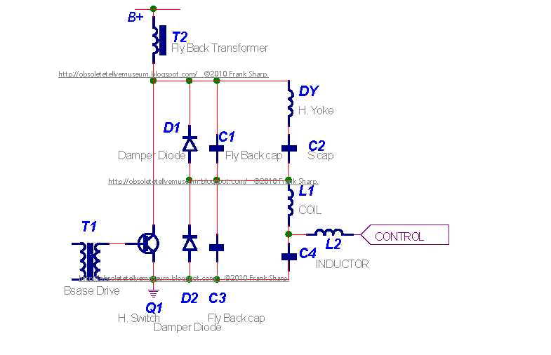 SPLIT DIODE MODULATOR
This horizontal circuit consists of two parts. D1, C1, C2 and DY are the components as described above.
D2, C3, C4 and L1 are a second “dummy” horizontal section that does not cause deflection current. By the
D.C. analyzing this circuit the voltage across C2 + C4 must equal the supply voltage (B+). Deflection
current in the DY is related to the supply voltage minus the voltage across C4. For a maximum horizontal
size the control point must be held at ground. This causes the dummy section to not operate and the DY
section will get full supply voltage. If the control point is at 1/3 supply then the DY section will be
operating at 2/3 supply.
Note: The impedance of (D1,C1,C2 and DY) and (D2,C3,C4 and L1) makes a voltage divider. If the
control point is not connected then there is some natural voltage on C4. Most split diode monitors are built
to pull power from the dummy section through L2 to ground. A single power transistor shunts from the
control point to ground. It is true that power can be supplied from some other supply through L2 to rise the voltage on C4. For maximum range a bi-directional power amplifier can drive the control point.
The most exciting feature if the split diode modulator is that the flyback pulse, as seen by the flyback
transformer, is the same size at all horizontal size settings.
HORIZONTAL SWITCH/DAMPER DIODEOn the right hand side of the screen, the H. switch transistor conducts current through the deflection yoke.
This current comes from the S correction capacitors, which have a charge equal to the effective supply
voltage. The damper diode allows current for the left hand side of the screen to flow back through the
deflection yoke to the S capacitors.
FLYBACK CAPACITOR
The flyback capacitor connects the hot side of the yoke to ground. This component determines the size and
length of the flyback pulse. ‘Tuning the flyback capacitor’ is done to match the timing of the flyback pulse
to the video blanking time of the video signal. The peak flyback voltage on the horizontal switch must be
set to less that 80% if the Vces specification. The two conditions of time and voltage can be set by three
variables (supply voltage, retrace capacitor and yoke inductance) .
S CAPACITOR
The S capacitors corrects outside versus center linearity in the horizontal scan. The voltage on the S cap
has a parabola plus the DC horizontal supply. Reducing the value of S cap increases this parabola thus
reducing the size of the outside characters and increasing the size of the center characters.
S Capacitor value: Too low: picture will be squashed towards edges.
Too high: picture will be stretched towards edges.
modified into a slightly sine-wave shape. This reduces the scanning speed near the
edges where the yoke is more sensitive. Generally the deflection angle of the electron
beam and the yoke current are closely related. The problem is the deflection angle
verses the distance of movement on the CRT screen does not have a linear effect.
BASE DRIVE CURRENT
The base drive resistor determines the amount of
base drive. If the transistor is over driven the Vsat
looks very good, but the current fall time is poor.
If the base current is too small the current fall time is very fast. The problem is that the transistor will have many volts across C-E when closed.
The best condition is found by placing the transistor in the heaviest load condition. Adjust the base resistor for the least power consumption then increase the base drive a small amount. This will slightly over drive the base.
GENERAL BASIC TRANSISTOR LINE OUTPUT STAGE OPERATION:
The basic essentials of a transistor line output stage are shown in Fig. 1(a). They comprise: a line output transformer which provides the d.c. feed to the line output transistor and serves mainly to generate the high -voltage pulse from which the e.h.t. is derived, and also in practice other supplies for various sections of the receiver; the line output transistor and its parallel efficiency diode which form a bidirectional switch; a tuning capacitor which resonates with the line output transformer primary winding and the scan coils to determine the flyback time; and the scan coils, with a series capacitor which provides a d.c. block and also serves to provide slight integration of the deflection current to compensate for the scan distortion that would otherwise be present due to the use of flat screen, wide deflection angle c.r.t.s. This basic circuit is widely used in small -screen portable receivers with little elaboration - some use a pnp output transistor however, with its collector connected to chassis.
Circuit Variations:
Variations to the basic circuit commonly found include: transposition of the scan coils and the correction capacitor; connection of the line output transformer primary winding and its e.h.t. overwinding in series; connection of the deflection components to a tap on the transformer to obtain correct matching of the components and conditions in the stage; use of a boost diode which operates in identical manner to the arrangement used in valve line output stages, thereby increasing the effective supply to the stage; omission of the efficiency diode where the stage is operated from an h.t. line, the collector -base junction of the line output transistor then providing the efficiency diode action without, in doing so, producing scan distortion; addition of inductors to provide linearity and width adjustment; use of a pair of series -connected line output transistors in some large -screen colour chassis; and in colour sets the addition of line convergence circuitry which is normally connected in series between the line scan coils and chassis. These variations on the basic circuit do not alter the basic mode of operation however.
Resonance

The most important fact to appreciate about the circuit is that when the transistor and diode are cut off during the flyback period - when the beam is being rapidly returned from the right-hand side of the screen to the left-hand side the tuning capacitor together with the scan coils and the primary winding of the line output transformer form a parallel resonant circuit: the equivalent circuit is shown in Fig. 1(b). The line output transformer primary winding and the tuning capacitor as drawn in Fig. 1(a) may look like a series tuned circuit, but from the signal point of view the end of the transformer primary winding connected to the power supply is earthy, giving the equivalent arrangement shown in Fig. 1(b).
The Flyback Period:
Since the operation of the circuit depends mainly upon what happens during the line flyback period, the simplest point at which to break into the scanning cycle is at the end of the forward scan, i.e. with the
 beam deflected to the right-hand side of the screen, see Fig. 2. At
this point the line output transistor is suddenly switched off by the
squarewave drive applied to its base. Prior to this action a linearly
increasing current has been flowing in the line output transformer
primary winding and the scan coils, and as a result magnetic fields have
been built up around these components. When the transistor is switched
off these fields collapse, maintaining a flow of current which rapidly
decays to zero and returns the beam to the centre of the screen. This
flow of current charges the tuning capacitor, and the voltage at A rises
to a high positive value - of the order of 1- 2k V in large -screen
sets, 200V in the case of mains/battery portable sets. The e
beam deflected to the right-hand side of the screen, see Fig. 2. At
this point the line output transistor is suddenly switched off by the
squarewave drive applied to its base. Prior to this action a linearly
increasing current has been flowing in the line output transformer
primary winding and the scan coils, and as a result magnetic fields have
been built up around these components. When the transistor is switched
off these fields collapse, maintaining a flow of current which rapidly
decays to zero and returns the beam to the centre of the screen. This
flow of current charges the tuning capacitor, and the voltage at A rises
to a high positive value - of the order of 1- 2k V in large -screen
sets, 200V in the case of mains/battery portable sets. The e nergy
in the circuit is now stored in the tuning capacitor which next
discharges, reversing the flow of current in the circuit with the result
that the beam is rapidly deflected to the left-hand side of the screen -
see Fig. 3. When the tuning capacitor has discharged, the voltage at A
has fallen to zero and the circuit energy is once more stored in the
form of magnetic fields around the inductive components. One half -cycle
of oscillation has occurred, and the flyback is complete.
nergy
in the circuit is now stored in the tuning capacitor which next
discharges, reversing the flow of current in the circuit with the result
that the beam is rapidly deflected to the left-hand side of the screen -
see Fig. 3. When the tuning capacitor has discharged, the voltage at A
has fallen to zero and the circuit energy is once more stored in the
form of magnetic fields around the inductive components. One half -cycle
of oscillation has occurred, and the flyback is complete.Energy Recovery:
First Part of Forward Scan The circuit then tries to continue the cycle of oscillation, i.e. the magnetic fields again collapse, maintaining a current flow which this time would charge the tuning capacitor negatively (upper plate). When the voltage at A reaches about -0.6V however the efficiency diode becomes forward biased and switches on. This damps the circuit, preventing further oscillation, but the magnetic fields continue to collapse and in doing so produce a linearly decaying current flow which provides the first part of the forward s
 can,
the beam returning towards the centre of the screen - see Fig. 4. The
diode shorts out the tuning capacitor but the scan correction capacitor
charges during this period, its right-hand plate becoming positive with
respect to its left-hand plate, i.e. point A. Completion of Forward Scan
When the current falls to zero, the diode will switch off. Shortly
before this state of affairs is reached however the transistor is
switched on. In practice this is usually about a third of the way
through the scan. The squarewave applied to its base drives it rapidly
to saturation, clamping the vol
can,
the beam returning towards the centre of the screen - see Fig. 4. The
diode shorts out the tuning capacitor but the scan correction capacitor
charges during this period, its right-hand plate becoming positive with
respect to its left-hand plate, i.e. point A. Completion of Forward Scan
When the current falls to zero, the diode will switch off. Shortly
before this state of affairs is reached however the transistor is
switched on. In practice this is usually about a third of the way
through the scan. The squarewave applied to its base drives it rapidly
to saturation, clamping the vol tage
at point A at a small positive value - the collector emitter saturation
voltage of the transistor. Current now flows via the transistor and the
primary winding of the line output transformer, the scan correction
capacitor discharges, and the resultant flow of current in the line scan
coils drives the beam to the right-hand side of the screen see Fig. 5.
tage
at point A at a small positive value - the collector emitter saturation
voltage of the transistor. Current now flows via the transistor and the
primary winding of the line output transformer, the scan correction
capacitor discharges, and the resultant flow of current in the line scan
coils drives the beam to the right-hand side of the screen see Fig. 5.Efficiency:
The transistor is then cut off again, to give the flyback, and the cycle of events recurs. The efficiency of the circuit is high since there is negligible resistance present. Energy is fed into the circuit in the form of the magnetic fields that build up when the output transistor is switched on. This action connects the line output transformer primary winding across the supply, and as a result a linearly increasing current flows through it. Since the width is
dependent on the supply voltage, this must be stabilised.
Harmonic Tuning:
There is another oscillatory action in the circuit during the flyback period. The considerable leakage inductance between the primary and the e.h.t. windings of the line output transformer, and the appreciable self -capacitance present, form a tuned circuit which is shocked into oscillation by the flyback pulse. Unless this oscillation is controlled, it will continue into and modulate the scan. The technique used to overcome this effect is to tune the leakage inductance and the associated capacitance to an odd harmonic of the line flyback oscillation frequency. By doing this the oscillatory actions present at the beginning of the scan cancel. Either third or fifth harmonic tuning is used. Third harmonic tuning also has the effect of increasing the amplitude of the e.h.t. pulse, and is generally used where a half -wave e.h.t. rectifier is employed. Fifth harmonic tuning results in a flat-topped e.h.t. pulse, giving improved e.h.t. regulation, and is generally used where an e.h.t. tripler is employed to produce the e.h.t. The tuning is mainly built into the line output transformer, though an external variable inductance is commonly found in colour chassis so that the tuning can be adjusted. With a following post I will go into the subject of modern TV line timebases in greater detail with other models and technology shown here at Obsolete Technology Tellye !
BU2 08(A)
08(A)
Silicon NPNnpn transistors,pnp transistors,transistors
Category: NPN Transistor, Transistor
MHz: <1 MHz
Amps: 5A
Volts: 1500V
HIGH VOLTAGE CAPABILITY
JEDEC TO-3 METAL CASE.
DESCRIPTION
The BU208A, BU508A and BU508AFI are
manufactured using Multiepitaxial Mesa
technology for cost-effective high performance
and use a Hollow Emitter structure to enhance
switching speeds.
APPLICATIONS:
* HORIZONTAL DEFLECTION FOR COLOUR TV With 110° or even 90° degree of deflection angle.
ABSOLUTE MAXIMUM RATINGS
Symbol Parameter Value Unit
VCES Collector-Emit ter Voltage (VBE = 0) 1500 V
VCEO Collector-Emit ter Voltage (IB = 0) 700 V
VEBO Emitter-Base Voltage (IC = 0) 10 V
IC Collector Current 8 A
ICM Collector Peak Current (tp < 5 ms) 15 A
TO - 3 TO - 218 ISOWATT218
Ptot Total Dissipation at Tc = 25 oC 150 125 50 W
Tstg Storage Temperature -65 to 175 -65 to 150 -65 to 150 oC
Tj Max. Operating Junction Temperature 175 150 150 °C
TDA1950 (itt), Line Circuits for TV Receivers (18-Pin Plastic Package)

These integrated circuits are advanced versions of the well-known types TDA1940, TDA1940F, TDA1950 and TDA1950F are identical
TBA940/950, TDA9400/9500 etc. integrated line oscillator circuits. except the following: at pin 2 the types having the suffix "F" supply ,
They comprise all stages for sync separation and line synchronisation horizontal output pulses of longer duration compared with the basic I
in TV receivers in one single silicon chip. Due to their high degree of types Integration, the number of external components is very small.
This integrated circuit contains the horizontal sweep generator (HO), the amplitude filter (AS), the sync-signal separating circuit (SA) and the frequency/phase comparator (FP). For the purpose of suppressing noise pulses which are caused via the operating voltage during the upper and the lower inversion point of the horizontal sweep generator (HO) which contains a single capacitor (C) and a first threshold stage circuit (SS1) with two fixed thresholds, there are provided a second and a third threshold stage circuit (SS2, SS3), to the inputs of which the sawtooth signal is applied, and with the thresholds thereof, approximately 2 μs prior to reaching the upper or the lower peak value of the sawtooth signal, are being passed through thereby. The output signal of the second threshold circuit (SS2) and the output signal of the third threshold stage circuit (SS3) which is applied via the pulse shaper circuit (IF), are superimposed linearly and, via the stopper circuit (blocking stage) (SP) serve to control the application of the composite video signal (BAS) to the amplitude filter (AS), or else they are applied to a clamping circuit which serves to apply the operating points of the amplitude filter (AS) and/or of the sync-signal separating circuit (SA) to such a potential that these two stages, for the time duration of these output pulses, are prevented from operating.
1. An integrated circuit for color television receivers, comprising a voltage- or current-controlled horizontal sweep generator (HO), an amplitude filter (AS), a synchronizing-signal separating circuit (SA) and a frequency/phase comparator (FP) which serves to synchronize the horizontal sweep generator (HO), with said generator being a sawtooth generator containing a single capacitor
(C) and a first threshold stage circuit (SS1) having two fixed thresholds, said integrated circuit further comprising:a second and a third threshold stage circuit (SS2, SS3) each being supplied with the sawtooth signal on the input side, comprising each time one threshold which, approximately 2μs prior to the reaching of the upper or the lower peak value of the sawtooth signal, is being passed thereby;
a pulse shaper circuit (IF) coupled to the output of said third threshold stage circuit (SS3) which pulse shaper circuit reduces the duration of the output pulse thereof to about the duration of the output pulse of said second threshold stage circuit (SS2), and
a stopper circuit (blocking stage) (SP) coupled to the outputs of both said pulse shaper circuit (IF) and said second threshold stage circuit (SS2), said stopper circuit having a signal input to which there is applied a composite video signal (BAS) and a signal output which is coupled to the input of said amplitude filter (AS).
2. The invention of claim 1 wherein the outputs of both said pulse shaper circuit (IF) and said second threshold stage circuit (SS2) are coupled to a clamping circuit which applies the operating points of said amplitude filter (AS) and said sync-separating signal (SA) to such a potential that they are prevented from operating.
3. An integrated horizontal sweep circuit comprising:
a generator for generating a sawtooth signal;
an amplitude filter having an input for receiving a composite video signal and having an output;
a sync-signal separating circuit having an input coupled to said amplitude filter output and having an output;
a frequency/phase comparator having a first input coupled to said separating circuit output,
a second input receiving said sawtooth signal and an output for controlling said generator; and
a control circuit responsive to said sawtooth signal for inhibiting said composite video signal when said sawtooth signal is within predetermined signal level ranges about the upper and lower inversion points of said sawtooth signal.
4. An integrated circuit in accordance with claim 3 wherein:
said generator comprises a capacitor, circuit means for charging and discharging said capacitor, and a first threshold circuit controlling said circuit means in response to said sawtooth signal reaching a first level corresponding to said first inversion point and a second level corresponding to said second inversion point.
5. An integrated horizontal sweep circuit comprising:
a sawtooth signal generator;
an amplitude filter having an input receiving a composite video signal and having an output;
a sync-signal separating circuit having an input coupled to said amplitude filter output and having an output;
a frequency/phase comparator having a first input coupled to said separating circuit output, a second input receiving said sawtooth signal and an output for controlling said generator; and
a control circuit responsive to said sawtooth signal for inhibiting operation of said amplitude filter and/or said sync-signal separating circuit when said sawtooth signal is within predetermined signal level ranges about the upper and lower inversion point of said sawtooth signal.
6. An integrated circuit in accordance with claim 5 wherein:
said generator comprises a capacitor, circuit means for charging and discharging said capacitor and a first threshold circuit controlling said circuit means in response to said sawtooth signal reaching a first level corresponding to said first inversion point and a second level corresponding to said second inversion point.
Description:
BACKGROUND OF THE INVENTIONThe invention relates to an integrated circuit for (color) television receivers, comprising a voltage- or current-controlled horizontal-sweep generator, an amplitude filter, a synchronizing signal separating circuit (sync-separator) and a frequency/phase comparator which serves to synchronize the horizontal sweep generator which is a sawtooth generator consisting of a single capacitor and of a first threshold stage having two fixed switching thresholds, cf. preamble of the patent claim. Such types of integrated circuits, for example, are known from th
e technical journal "Elektronik aktuell", 1976, No. 2, pp. 7 to 14 where they are referred to as TDA 9400 and TDA 9500.Especially on account of the fact that the amplitude filter as well as the horizontal sweep generator in the form of the aforementioned sawtooth generator, are integrated on a single semiconductor body, it is likely that noise interference pulses coming from the individual stages, and via the supply voltage line, may have a disturbing influence upon the horizontal sweep generator, i.e. upon the threshold stage thereof, in such a way that either the lower or the upper or successively both switching thresholds are exceeded before the time by the voltage at the capacitor, owing to the noise superposition, so that the generator will show to have a "wrong" frequency or phase position. This frequency/phase variation, of course, is compensated for by the circuit, with the aid of the synchronzing pulses, but only in such a way that the noise effect remains visible in the television picture.
SUMMARY OF THE INVENTION
The invention is characterized in the claim is aimed at overcoming this drawback by solving the problem of designing an integrated circuit of the type described in greater detail hereinbefore, in such a way that noise pulses acting upon the capacitor voltage or the internal reference voltages for the switching thresholds (see below) in the proximity of the two switching thresholds, are prevented from having the described disadvantageous effect. Accordingly, an advantage of the invention results directly from solving the given problem.
Other objects, features and advantages of the present invention will become more fully apparent from the following detailed description of the preferred embodiment, the appended claims and the accompanying drawing in which:
BRIEF DESCRIPTION OF THE INVENTION
The invention will now be described in greater detail with reference to the accompanying drawing. This drawing, in the form of a schematical circuit diagram, shows the construction of an integrated circuit according to the invention.
DETAILED DESCRIPTION OF THE INVENTION
T
he horizontal sweep generator HO comprises the capacitor C as connected to the zero point of the circuit, and which is charged and discharged via the two shown constant current sources CS1 and CS2, thus causing the intended sawtooth voltage to appear thereat. Moreover, the horizontal sweep generator HO comprises the first threshold stage circuit SS1, having an upper and a lower threshold. As soon as the capacitor voltage exceeds one of the thresholds, the first threshold stage circuit SS1 switches over to the other threshold. The two thresholds are defined by the voltage divider P as connected to the operating voltage U, and in which the corresponding threshold inputs are connected to corresponding tapping points. The output of the threshold stage circuit SS1 controls the electronic switch S, so that the constant current source CS2 as connected thereto, is either disconnected from or connected to the zero point of the circuit. Accordingly, in the disconnected state, the capacitor C is charged via the constant current source CS1 arranged in series therewith while in the connected state the capacitor C is discharged across the aforementioned constant current source CS2 arranged in parallel therewith, if, as a matter of fact, the current of the constant current source CS1 arranged in series with the capacitor C, is smaller than that of the parallel-arranged constant current source CS2.Now, for the purpose of avoiding the aforementioned drawbacks, there is provided a second and a third threshold stage circuit SS2 and SS3, respectively, as well as the pulse shaper circuit IF. To the respective input of the two threshold stage circuits SS2, SS3, there is applied the capacitor voltage, in the form of the sawtooth signal, and these stages have a threshold voltage which, approximately 2 μs prior to the reaching of the upper or the lower peak value of the sawtooth voltage, is being passed thereby. This means to imply that the threshold voltage of the second threshold stage circuit SS2 is somewhat lower than the voltage of the upper threshold of the first threshold stage circuit SS1, and that the threshold voltage of the third threshold stage circuit SS3 is somewhat higher than the voltage of the lower threshold of the first threshold stage circuit SS1. The two thresholds of the threshold stage circuits SS2, SS3 can thus be realized in a simple way by providing further tapping points at the voltage divider P, as is shown in the accompanying drawing. Thus, the second threshold stage circuit SS2 is provided for at a voltage divider tapping point below the tapping point chosen for the upper threshold, and the tapping point for the third threshold stage circuit SS3 is provided for above the tapping point which has been chosen for the lower threshold of the first threshold stage circuit SS1.
Since, within the area of the lower inversion point of the sawtooth signal there results an excessively wide output pulse of the third threshold stage circuit SS3, the pulse shaper circuit IF is arranged subsequently thereto, for reducing the duration of the output pulse as applied to its input, to about the duration of the output pulse of the second threshold stage circuit SS2. This pulse shaper circuit IF, for example, may be realized by a monoflop, in particular by a digital monoflop (=monostable circuit).
The output pulses of the second threshold stage circuit SS2 and of the pulse shaper circuit IF are then super-positioned linearly, with this being denoted in the drawing by a simple interconnection of the two respective lines. The combined signal is applied to the input of the stopper circuit (blocking stage) SP, to the signal input of which there is fed the composite video signal BAS, and the output thereof controls both the amplitude filter AS and the synchronizing signal separating circuit SA.
The combined signal may also be used to control a clamping circuit applying the operating points of the amplitude filter AS and/or of the sync-signal-separating circuit SA to such a potential which prevents it from operating.
If now the sawtooth signal reaches the range of its upper or its lower inversion point, the composite video signal BAS is not applied to either the amplitude filter AS or the sync-signal separating circuit SA, so that shortly before and shortly after the inversion points, signals are prevented from being processed in the two stages AS, SA. This, in turn, has the consequence that during these times noise pulses are prevented from superimposing upon the operating voltage U, so that there is also prevented an unintended triggering of the first threshold stage circuit SS1.
Moreover, it is still shown in the drawing that the amplitude filter AS, the sync-signal separating circuit SA and the frequency/phase comparator FP are arranged in series in terms of signal flow, with the latter, in addition, receiving the sawtooth signal, and with the output signal thereof acting upon the two current sources in a regulating sense. In the drawing, this is indicated by the setting arrows at the two current sources.
While the present invention has been disclosed in connection with the preferred embodiment thereof, it should be understood that there may be other embodiments which fall within the spirit and scope of the invention as defined by the following claims.
No comments:
Post a Comment
The most important thing to remember about the Comment Rules is this:
The determination of whether any comment is in compliance is at the sole discretion of this blog’s owner.
Comments on this blog may be blocked or deleted at any time.
Fair people are getting fair reply. Spam and useless crap and filthy comments / scrapers / observations goes all directly to My Private HELL without even appearing in public !!!
The fact that a comment is permitted in no way constitutes an endorsement of any view expressed, fact alleged, or link provided in that comment by the administrator of this site.
This means that there may be a delay between the submission and the eventual appearance of your comment.
Requiring blog comments to obey well-defined rules does not infringe on the free speech of commenters.
Resisting the tide of post-modernity may be difficult, but I will attempt it anyway.
Your choice.........Live or DIE.
That indeed is where your liberty lies.
Note: Only a member of this blog may post a comment.