


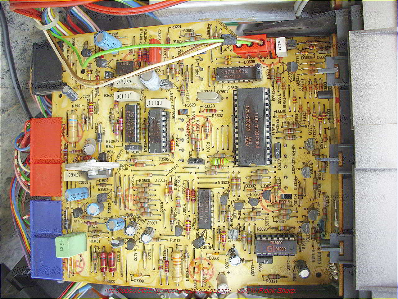


The METZ CHASSIS 680g is a higly sophisticated chassis even if not seems to be.
Particularly in power supply you can see the high engineering present at METZ and further example of that kind of engineering and building culture you can see .
It's semi modular and it's supplyed directly by mains.
These were higly reliable and they were running almost cool.
Tuning system in this set is introducing, even with others models, the Ucontroller NEC for all functions programmed by METZ and fabricated by NEC.
It's semi modular and it's supplyed directly by mains.
These were higly reliable and they were running almost cool.
Tuning system in this set is introducing, even with others models, the Ucontroller NEC for all functions programmed by METZ and fabricated by NEC.
All components from discretes to semiconductors are almost PHILIPS Made.
This version is featuring a VST TUNING SEARCH SYSTEM
This version is featuring a VST TUNING SEARCH SYSTEM


-MAIN CONTROL SYSTEM/TUNING with NEC KOZ026-049 + SAB3013 + 2 X SN74LS26N +ER1400
- I.F. UNIT 682ZF8017 WITH TDA2541 + TDA2545
- SOUND UNIT WITH TDA2006 + TBA120T 678NF5507/C
- FRAME DEFLECTION UNIT 680VA0012
- LUMINANCE CHROMINANCE UNIT 678LC0012 TDA2524 + TDA2560
- RGB AMPLIFIER + MATRIX 678VE0010 WITH TDA2532.
- SUPPLY CONTROL + REGULATOR + PROTECT 680RS0010
TDA2560 LUMINANCE AND CHROMINANCE CONTROL COMBINATION
The TDA2560 is a monolithic integrated circuit for use in decoding systems of COLOR
television receivers. The circuit consists of a luminance and chrominance amplifier.
The luminance amplifier has a low input impedance so that matching of the luminance
delay line is very easy.
It also incorporates the following functions:
- d.c. contrast control;

- d.c. brightness control;
- black level clamp;
- blanking;
- additional video output with positive-going sync.
The chrominance amplifier comprises:
- gain controlled amplifier;
- chrominance gain control tracked with contrast control;
- separate d.c. saturation control:
- combined chroma and burst output, burst signal amplitude not affected by contrast and
saturation control;
- the delay line can be driven directly ‘by the IC.
APPLICATION INFORMATION (continued)
The function is quoted against the corresponding pin number
Balanced chrominance input signal (in conjunction with pin 2)
This is derived from the chrominance signal bandpass filter, designed to provide a
push-pull input. A signal amplitude of at least 4 mV peak-to-peak is required
between pins l and 2. The chrominance amplifier is stabilized by an external feedback
loop from the output (pin 6) to the input (pins I and 2). The required level at pins l
and 2 will be 3 V.
All figures for the chrominance signals are based on a colour bar signal with 75%
saturation: i.e. burst-to-chrominance ratio of input signal is 1 1 2.
Chrominance signal input (see pin 1)
A. C.C. input
A negative-going potential, starting at +l,2 V, gives a 40 dB range of a. c. c.
Maximum gain reduction is achieved at an input voltage of 500 mV.
Chrominance saturation control
A control range of +6 dB to >-14 dB is provided over a range of d. c. potential on
pin 4 from +2 to +4 V. The saturation control is a linear function of the control
voltage.
Negative supply (earth)
Chro minance signal output
For nominal settings of saturation and contrast controls (max. -6 dB for saturation,
and max. -3 dB for contrast) both the chroma' and burst are available at this pin, and
in the same ratio as at the input pins 1 and 2. The burst signal is not affected by the
saturation and contrast controls. The a.c. c. circuit of the TDA2522 will hold
constant the colour burst amplitude at the input of the TDA2522. As the PAL delay
line is situated here between the TDA256O and TDA2522 there may be some variation
of the nominal 1 V peak-to-peak burst output of the TDA2560, according to the
tolerances of the delay line. An external network is required from pin 6 of the
TDA256O to provide d. c. negative feedback in the chroma channel via pins I and 2.
Burst gating and clamping pulse input
A two-level pulse is required at this pin to be used for burst gate and black level
clamping. The black level clamp is activated when the pulse level is greater than
7 V. The timing of this interval should be such that no appreciable encroachment
occurs into the sync pulse on picture line periods during normal operation of the
receiver. The burst gate, which switches the gain of the chroma amplifier to
maximum, requires that the input pulse at pin 7 should be sufficiently wide, at least
8 ps, at the actuating level of 2,3 V.
+12 V power supply
Correct operation occurs within the range 10 to 14 V. All signal and control levels
have a linear dependency on supply voltage but, in any given receiver design, this
range may be restricted due to considerations of tracking between the power supply
variations and picture contrast and chroma levels.
Flyback blanking input waveform
This pin is used for blanking the luminance amplifier. When the input pulse exceeds
the +2, 5 Vlevel, the output signal is blanked to a level of about 0 V. When the input
exceeds a +6 V level, a fixed level of about 1, 5 V is inserted in the output. This
level can be used for clamping purposes.
Luminance sigal output
An emitter follower provides a low impedance output signal of 3 V black-to-white
amplitude at nominal contrast setting having a black level in the range 1 to 3 V. An
external emitter load resistor is not required.
The luminance amplitude available for nominal contrast may be modified according
to the resistor value from pin 13 to the +12 V supply. At an input bias current
114 of 0,25 mA during black level the amplifier is compensated so that no black
level shift more than 10 mV occurs at contrast control. When the input current
deviates from the quoted value the black level shift amounts to 100 mV/rnA.
Brightness control
The black level at the luminance output (pin 10) is identical to the control voltage
required at this pin, A range of black level from l to 3 V may be obtained.
Black level clamp capacitor
Luminance gain setting resistor
The gain of the luminance amplifier may be adjusted by selection of the resistor
value from pin 13 to +12 V. Nominal luminance output amplitude is then 3 V
black-to-white at pin 10 when this resistor is 2, 7 l
SAB3034 COMPUTER INTERFACE FOR TUNING AND CONTROL (CITAC)
GENERAL DESCRIPTION
The SAB3034 provides closed-loop digital tuning of TV receivers, with or without a.f.c., as required. lt
also controls up to 8 analogue functions, 4 general purpose I/O ports and 4 high-current outputs for
tuner band selection.
The IC is used in conjunction with a microcomputer from the MAB84OO family and is controlled via a two-wire, bidirectional I2 C bus.
Featu res
Combined analogue and digital circuitry minimizes the number of additional interfacing components
required
Frequency measurement with resolution of 50 KHz
Selectable prescaler divisor of 64 or 256
32 V tuning voltage amplifier
4 high-current outputs for direct band selection
8 static digital to analogue converters (DACSI for control of analogue functions
Four general purpose input/output (l/O) ports
Tuning with control of speed and direction
Tuning with or without a.f.c.
Single-pin, 4 MHZ on-chip oscillator
I2 C bus slave transceiver
FUNCTIONAL DESCRIPTION
The SAB3034 is a monolithic computer interface which provides tuning and control functions and
operates in conjunction with a microcomputer via an I2 C bus.
Tuning
This is performed using frequency-locked loop digital control. Data corresponding to the required tuner
frequency is stored in a 15-bit frequency buffer. The actual tuner frequency, divided by a factor of 256
(or by 64) by a prescaler, is applied via a gate to a 15-bit frequency counter. This input (FDIV) is
measured over a period controlled by a time reference counter and is compared with the contents of the frequency buffer. The result of the comparison is used to control the tuning voltage so that the tuner frequency equals the contents of the frequency buffer multiplied by 50 kHz within a programmable tuning window (TUW).
The system cycles over a period of 6,4 ms (or 2,56 ms), controlled by the time reference counter which is clocked by an on-chip 4 lVlHz reference oscillator. Regulation of the tuning voltage is performed by a charge pump frequency-locked loop system. The charge IT flowing into the tuning voltage amplifier is controlled by the tuning counter, 3-bit DAC and the charge pump circuit. The charge IT is linear with the frequency deviation Af in steps of 50
TDA2545A Quasi-split-sound circuitGENERAL DESCRIPTION The TDA2545A is a monolithic integrated circuit for quasi-split-sound processing in television receivers. Features · 3-stage gain controlled i.f. amplifier · A.G.C. circuit · Reference amplifier and limiter amplifier for vision carrier (V.C.) processing · Linear multiplier for quadrature demodulation.
TDA2541 IF AMPLIFIER WITH DEMODULATOR AND AFC

DESCRIPTION
The TDA2540 and 2541 are IF amplifier and A.M.
demodulator circuits for colour and black and white
television receivers using PNP or NPN tuners. They
are intended for reception of negative or positive
modulation CCIR standard.
They incorporate the following functions : .Gain controlled amplifier .Synchronous demodulator .White spot inverter .Video preamplifier with noise protection .Switchable AFC .AGC with noise gating .Tuner AGC output (NPN tuner for 2540)-(PNP
tuner for 2541) .VCR switch for video output inhibition (VCR
play back).
TDA2006 12W AUDIO AMPLIFIER
DESCRIPTION
The TDA2006 is a monolithic integrated circuit in
Pentawatt package, intended for use as a low
frequency class ”AB” amplifier. At ±12V, d = 10 %
typically it provides12Woutput poweron a 4W load
and 8W on a 8W . The TDA2006 provides high
output current and has very low harmonic and
cross-over distortion. Further the device incorporates
anoriginal (and patented)short circuit protection
system comprising an arrangement for
automatically limiting the dissipated power so as to
keep the working point of the output transistors
within their safe operating area. A conventional
thermal shutdown system is also included. The
TDA2006 is pin to pin equivalent to theTDA2030.
SHORT CIRCUIT PROTECTION
The TDA2006 has an original circuit which limits
the current of the output transistors.
This function can thereforebe considered as being
peak power limiting rather than simple current limiting.
It reduces the possibility that the device gets damaged
during an accidental short circuit from AC
output to ground.
THERMALSHUT DOWN
The presence of a thermal limiting circuit offers the
following advantages :
1) an overload on the output (even if it is
permanent), or an above l imi t ambient
temperature can be easily supported since the
Tj cannot be higher than 150°C.
2) the heatsink can have a smaller factor of safety
compared with that of a conventional circuit.
There is no possibility of device damage due to
high junction temperature.
If for any reason, the junction temperature increases
up to 150 °C, the thermal shutdown simply
reduces the power dissipation and the current consumption.
The maximum allowable power dissipation depends
upon the size of the external heatsink (i.e.
its thermal resistance)
METZ HAITI COLOR 7173 CHASSIS 680G Power supply regulator for television:
1. A television apparatus power supply, comprising:
a source of an input supply voltage;
a source of an on/off control signal that selectively contains power-on and power-off control information that is indicative when an operation of said power supply in a normal operation power-up mode is required and when in a standby mode is required, respectively;
means responsive to said on/off control signal and coupled to said input supply voltage for generating therefrom a first supply voltage during a normal operation power-up mode of said power supply;
means coupled to said input supply voltage for generating therefrom a second supply voltage that is coupled to a first terminal of a first load circuit to develop thereat a first terminal supply voltage during s
aid standby mode;switching means coupled between said first supply voltage and said first terminal for coupling during said power-up mode said first supply voltage to said first terminal to develop during said power-up mode said first terminal supply voltage at said first terminal; and
a voltage regulator coupled to said first terminal for regulating said first terminal supply voltage such that said regulated first terminal supply voltage is coupled through said switching means during said power-up mode to a second terminal of said switching means to regulate thereat a third supply voltage that during said standby mode is isolated by said switching means from said first terminal.
2. An apparatus according to claim 1 wherein said switching means comprises a diode.
3. An apparatus according to claim 1 further comprising, a transistor having a control electrode that is coupled to said third supply voltage at said second terminal, wherein a second load circuit is coupled to a main current conducting electrode of said transistor and wherein said switching means comprises a diode that is interposed between said control electrode of said transistor and said forst terminal supply voltage and a resistor coupled between said diode and said first supply voltage that cuases said diode to be conductive only when said first supply voltage is generated.
4. An apparatus according to claim 3 wherein said diode isolates said first supply voltage generating means from said second supply voltage during said standby mode.
5. An apparatus according to claim 4 wherein said diode isolates said first supply voltage generating means from said second load during said standby mode when said first supply voltage is turned-off.
6. An apparatus according to claim 3 wherein said diode provides temperature compensation for variations of a base-emitter junction voltage in said transistor to produce a temperature compensated output supply voltage at an emitter electrode of said transistor.
7. An apparatus according to claim 1 wherein said first supply voltage generating means comprises a deflection circuit, responsive to a control signal at a frequency that is related to a deflection frequency, that includes a flyback transformer for producing, when said signal at said deflection related frequency is generated, said first supply voltage from a voltage that is developed at said flyback transformer and wherein said regulated first terminal supply voltage is coupled to a control circuit that generates said control signal at said deflection related frequency for energizing said control circuit.
8. An apparatus according to claim 7 wherein said control circuit generates said control signal that is a pulse-width modulated control signal.
9. An apparatus according to claim 1 wherein said second supply voltage generating means comprises a step-down transformer coupled to said input supply voltage, and a rectifier having an input terminal that is coupled to said step-down transformer for generating said second supply voltage by rectifying a voltage that is developed at said step-down transformer.
10. An apparatus according to claim 1 wherein said first supply voltage generating means comprises a deflection circuit having a flyback transformer for generating in a winding of said flyback transformer a voltage at a frequency that is related to a deflection frequency and a rectifier coupled to said winding of said flyback transformer for generating from a voltage that is generated in said winding said first supply voltage.
11. An apparatus according to claim 1 wherein said source of said on/off control signal comprises a remote receiver.
12. An apparatus according to claim 1 further comprising a third load circuit coupled to said first supply voltage generating means wherein said switching means isolates said first terminal from said third load circuit during said standby mode.
13. A television apparatus power supply, comprising:
a source of a start-up supply voltage;
a run-mode power supply for developing in a run-mode a run-supply voltage, said run-mode power supply having a first terminal that is coupled to said start-up supply voltage for developing a first terminal supply voltage at said first terminal during a start-up interval;
switching means coupled to said first terminal and to said source of run-supply voltage for applying said run supply voltage to said first terminal to develop said first terminal supply voltage at said terminal during operation in said run-mode; and
an emitter follower stage having an input terminal that is coupled to said first terminal via said switching means during said run-mode and having an output terminal coupled to a load and a third terminal that is coupled to said source of run supply voltage for supplying main current from said output terminal to said load during operation in said run-mode at an applied voltage level that is regulated in accordance with said first terminal supply voltage.
14. A television apparatus power supply, comprising:
a source of an input supply voltage;
means coupled to said input supply voltage for generating therefrom a first supply voltage during a normal operation power-up mode of said power supply;
means coupled to said input supply voltage for generating therefrom a second supply voltage that is coupled to a first terminal of a first load circuit to develop thereat a first terminal supply voltage prior to the operation in said power-up mode;
switching means coupled between said first supply voltage and said first terminal for coupling during said power-up mode said first supply voltage to said first terminal to develop during said power-up mode said first terminal supply voltage at said first terminal; and
a voltage regulator coupled to said first terminal for regulating said first terminal supply voltage such that said regulated first terminal supply voltage is coupled through said switching means during said power-up mode to a second terminal of said switching means to regulate thereat a third supply voltage that prior to the operation in said power-up mode is isolated by said switching means from said first terminal.
15. An apparatus according to claim 1 wherein said switching means comprises a diode.
16. An apparatus according to claim 14 further comprising, a transistor having a control electrode that is coupled to said third supply voltage at said second terminal, wherein a second load circuit is coupled to a main current conducting electrode of said transistor and wherein said switching means comprises a diode that is interposed between said control electrode of said transistor and said first terminal supply voltage and a resistor coupled between said diode and said first supply voltage that causes said diode to be conductive only when said first supply voltage is generated.
17. An apparatus according to claim 16 wherein said diode isolates said first supply voltage generating meand from said second supply voltage during a standby mode of operation.
18. An apparatus according to claim 17 wherein said diode isolates said first supply voltage generating means from said second load during said standby mode when said first supply voltage is turned-off.
19. An apparatus according to claim 16 wherein said diode provides temperature compensation for variations of a base-emitter junction voltage in said transistor to produce a temperature compensated output supply voltage at an emitter electrode of said transistor.
20. An apparatus according to claim 14 wherein said first supply voltage generating means comprises a deflection circuit, responsive to a control signal at a frequency that is related to a deflection frequency, that includes a flyback transformer for producing, when said signal at said deflection related frequency is generated, said first supply voltage from a voltage that is developed at said flyback transformer and wherein said regulated first terminal supply voltage is coupled to a control circuit that generates said control signal at said deflection related frquency for energizing said control circuit.
Description:
The invention relates to an arrangement for regulating a run supply voltage of a television apparatus.
In, for example, a television receiver, a pulse-width modulator, or voltage regulator may generate a pulse-width modulated control signal, at a horizontal deflection related frequency. The control signal may be coupled to a power supply switching stag that supplies a regulated B+ supply voltge to a horizontal output stage. The voltage regulator circuitry may be combined with horizontal circuit (IC) that is referred to herein as the deflction IC. The deflection IC may be required to operate, selectively, in a power-up mode and in a standby mode, in accordance with an on/off control signal provided by a remote rceiver. Such pulse-width voltage regulator may be required to supply, in the power-up mode, the pulse-width modulated control signal for controlling the power supply that generates the regulated B+ supply voltage used for operating the horizontal output stage of the receiver. When operation in the standby mode is required, such control signal may be required t
o prevent the power supply from energizing the deflection output stage until such time as a user initiates a power-up command that is provided via the remote receiver.The deflection IC that includes, for example, the voltage regulator, may include other portions that are required to be energized during both the power-up and the standby modes. A second voltage regulator such as a shunt regulator integral to the IC, for example, may be coupled between a supply voltage receiving terminal of the deflection IC and ground for regulating the supply voltage of the deflection IC during both the power-up and standby modes. Similarly, the remote receiver may also be required to be energized during both the power-up mode and the standby mode.
A standby power supply for the deflection IC may include a standby transformer having a primary winding that is coupled to an alternating current (AC) mains supply source. A voltage that is developed at a secondary winding of the transformer may be rectified to produce a DC, standby energizing voltage. The standby energizing voltage may be applied to the supply voltage receiving terminal of the deflection IC to energize, for example, that portion of the deflection IC that is required to be energized by the standby power supply during the standby mode; whereas, during the power-up mode, the run-mode power supply provides the energizing voltage to such terminal. The shunt regulator may regulate the energizing voltage at such terminal during both the power-up and standby modes.
The regulated, energizing voltage, developed at the supply voltage receiving terminal during the power-up mode, may be at, for example, the same level that is required by other integrated circuits of the television receiver. Therefore, it may be desirable to utilize such regulatd energizing voltage to regulate a second supply voltage that is coupled to various other circuits of the television receiver and that provides a corresponding supply current during operation in the power-up mode.
It may be desirble to obtain such regulation of the second supply voltage with as few circuit components as possible. Furthermore, it may be desirable that, during operation in the standby mode, the second supply voltage generating and regulating circuitry will not load the standby power supply that is coupled to the supply voltage rceiving terminal of the deflection IC. Reduction of the supply current that is required from the tnadby transformer during the standby mode is desirable so as to reduc the cost of such transformer.
In accordance with an aspect of the invention, a television apparatus power supply generates a first supply voltage during a normal operation power-up mode of the power supply. a second supply voltage is coupled to a first terminal of a first load circuit to develop a first terminal supply voltage prior to operation in the power-up mode. A switching arrangement is coupled between the first supply voltage and the first terminal for coupling, during the power-up mod, the first supply voltage to the first terminal to develop, during the power-up mode, t
he first terminal supply voltage at the first terminal. A voltage regulator supply voltag such that the regulated first terminal supply voltage is coupled through the switching arrangement, during the power-up mode, to a second terminal of the switching arrangement to regulate at the second terminal a third supply voltage that, prior to the operation in the power-up mode, is isolated by the switching arrangment from the first terminal.The sole FIGURE illustrates a television power supply including a supply regulator embodying the invention.
The sole FIGURE illustrates a portion of a television reciever incorporating a deflection IC 100. Such portion of the television receiver includes a bridge rectifier 101 that rectifies a mains supply voltage VAC to produce a DC, unregulated voltage VUR. A conventionally designed output stage, or switch regulator 102 that may include a silicon controlled rectifier (SCR) produces, in a power-up mode, a regulated voltage B+ that is coupled to a flyback transformer T1. An input terminal 102c of regulator 102 is coupled to unregulated
 voltage VUR. Regulated voltage B+ is developed at an output terminal 102d of switch regulator 102. Transformer T1 is coupled to a collector electrode of a deflection switching transistor Q1 of a horizontal circuit output stage 99 operating at a horizontal rate fH. A control signal Hr, at the horizontal rate fH, that is produced in a corresponding portion of deflection IC 100, referred to herein as a horizontal processor 100a, is coupled via a horizontal driver 666 to the base electrode of transistor Q1. Signal Hr controls the switching of transistor Q1 to generate a deflection current iy in a deflection winding LY of output stage 99. A retrace voltage Vw2 is produced in a conventional manner across a winding W1 of tranformer T1 in each retrace interval of each horizontal period H. Each retrace interval occurs immediately after transistor Q1 becomes nonconductive. A DC, run-mode supply voltage V+, that is illustratively +16 volts, is produced by rectifying voltage Vw2 in a rectifier arrangement 104 that is coupled to winding W1. Voltage V+ is also coupled to various circuits of the receiver to provide them with energy during a power-up mode of the television receiver. Such circuits are depicted as a load 900.
Voltage V+ is also coupled to a corresponding portion of deflection IC 100 that is referred to herein as switch mode regulator and pre-driver 100b to provide a feedback signal. Regulator and pre-driver 100b generates a pulse width modulated signal Sc that controls the duration, in each horizontal interval H, in which switch regulator 102 is conductive. The duty cycle of signal Sc varies, in accordance with a difference between a voltage that is proportional to voltage V+ and a reference voltage VNIN that may be produced in a conventional manner. Signal Sc causes regulated voltage B+ to be at a predetermined DC voltage level such as, illustratively, +125 volts. Signal Sc, voltage B+ and voltage kV+ that may be produced in a conventionally known manner are produced, illustratively, when deflection IC 100 operates in the power-up mode, but are not produced during television receiver standby-mode operation.
A standby transformer T0 steps down voltage VAC. The stepped down voltage is rectified in a rectifier arrangement 106 to produce a standby voltage VSB. Standby voltage VSB is coupled to an energizing voltage receiving terminal 120 of deflection IC 100 through a resistor R1 that charges a capacitor 66 to produce in capacitor 66 an energizing voltage Vcc. Voltage Vcc is coupled to terminal 120 of deflection IC 100. Regulated voltage V+ is coupled to terminal 120 via a resistor R11, that is coupled in series with a diode D2, to supply voltage Vcc from voltage V+ only when deflecting IC 100 operates in the power-up mode. Diode D2 that is nonconductive during the standby mode prevents current drain via load 900 from standby transformer T0.
Standby voltage VSB is coupled to a remote receiver 107 to provide the o
perating voltage of remote receiver 107. Remote receiver 107 causes, via a drain of an MOS transistor 108, when transistor 108 is conductive, a a low impedance to be formed at a terminal 109 of deflection IC 100. The low impedance occurs after, for example, a user initiates a power-on command via an infra-red communication link that cuases a start-up interval to occur. When transistor 108 becomes conductive, it causes an on/off control circuit 555 to generate a control signal 555a that applies voltage Vcc to horizontal processor 100a; consequently, a horizontal oscillator, not shown in the FIGURES, of processor 100a begins operating and signal Hr is generated. Similarly, a control signal 555b of circuit 555 applies voltage Vcc to pre-driver 100b that causes pre-driver 100b to generate signal Sc.At the beginning of the start-up interval, horizontal driver 666 is energized by standby voltage VSB. Voltage Vcc is then obtained from the charge previously stored by arrangement 106 in capacitor 66. During the start-up interval, voltage V+ that was zero before begins increasing. At the end of the start-up interval, when voltage V+ is sufficiently large, it causes diode D2 to turn-on for supplying voltage Vcc in the power-up mode from voltage V+.
In the power-up mode, the television receiver is fully operative. Conversely, after a power-off command is initiated by the user, transistor 108 becomes nonconductive and forms a high impedance circuit at terminal 109 that causes a standby mode to occur. In the standby mode, deflection current iy and the raster on a display device of the television receiver are turned-off.
An input supply current iPS is coupled through terminal 120 to deflection IC 100 for providing the energizing current of deflection IC 100. During operation in the power-up mode, current iPS is supplied mainly by rectifier arrangement 104 through diode D2 and D4; whereas, during operation in the standby mode, current iPS is supplied from standby transformer 106 via rectifier arrangement 106 and resistor R1.
Voltage Vcc is regulated in deflection IC 100 by a shunt regulator 131 that is required to regulate voltage Vcc during operations in both the standby mode and the power-up mode. Regulation of voltage Vcc during the standby mode may be desirable for protecting deflection IC 100 from an over-voltage condition at terminal 120 that may occur should voltage Vcc exceed the voltage rating of deflection IC 100, during the standby mode. If permitted to occur, such over voltage condition may damage deflection IC 100. Voltage Vcc may also be required to be a regulated voltage, during the standby mode, for operating, for example, on/off control circuit 555 of deflection IC 100. Shunt regulator 131 regulates voltage Vcc, in accordance with a reference voltage VBG2, that is generated during both the power-up and standby modes. Voltage VBG2 is generated in, for example, in a bandgap type voltage source 105 that is, therefore, required to operate during both the standby and the power-up modes.
Various circuits in the receiver such as, for example, a second IC of the television reciver, that are depicted as a load 999 in the FIGURE, may require, during the power-up mode, a regulated supply voltage, that is depicted as a voltage VRUN in the FIGURE. Voltage VRUN may be required to be at a level that is equal to that of, for example, voltage Vcc. It may be desirable to utilize voltage Vcc that is regulated by shunt regulator 131 to also provide regulation of voltage VRUN.
In accordance with an aspect of the invention, a transistor Q2 having a collector electrode that is coupled to voltage V+ at a terminal 104a produces regulated voltage VRUN at a emitter electrode of transistor Q2. The base electrode of transistor Q2 is ocupled to the anode of diode D2. The base current of transistor Q2 is provided by resistor R111. The forward voltage drop across diode D2 is summed with voltage Vcc to produce at th
e base of transistor Q2 a voltage that is higher by diode D2 voltage drop that is, approximately, 0.7 volts in a silicon diode. Consequently, voltage VRUN that is smaller than the base voltage of transistor Q2 by, approximately, the same voltage drop that is developed across diode D2 is equal to voltage Vcc. A current iRUN that is supplied via transistor Q2 to load 999 is outside the current path of current iPS that is coupled to deflection IC 100 via terminal 120.In accordance with another aspect of the invention, temperature related changes of the voltage across the base-emitter junction of transistor Q2, are temperature compensated by diode D2 to render voltage VRUN regulated and temperature compensated. Furthermore, using a bandgap type voltage source such as source 105 for regulating voltage VRUN provides, advantageously, temperature compensation with tighter tolerances than obtained by using a zener diode that is used in some prior art circuits. Also, unlike a zener diode, the bandgap type voltage source can be designed to provide any selected voltage within a given range of voltages. Using resistor R111, diode D2 and shunt regulator 131, that are used for operating deflection IC 100, also for controlling transistor Q2 to obtain regulation of voltage VRUN, advantageously, eliminates the need for separate resistor, diode and regulator that would have, otherwise, been required for providing the base voltage of transistor Q2.
During operation in the power-up mode, voltage V+, that is ocupled via resistor R111, causes diode D2 to be conductive. Resistor R111 is required to developing a voltage drop that is equal to the difference between voltage V+ and a sum voltage of voltage Vcc and the forward voltage drop across diode D2.
During the standby mode it is undesirable to load transformer TO and capacitor 66 by any of load 900, load 999, resistor R111 and transistor Q2, because the cost of transformer TO is directly related to the standby current requirement from, or loading of, transformer T0. Diode D2, advantageously, prevents the loading of transformer T0 during the start-up interval, as long as voltage V+ is not sufficiently large to turn on diode D2. Similarly, during the standby mode, each of load 900, load 999, resistor R111 and transistor Q2 is, advantageously, isolated from standby transformer T0 by diode D2 that is switched off.
METZ 7173 HAITI COLOR CHASSIS 680G CIRCUIT ARRANGEMENT IN A PICTURE DISPLAY DEVICE UTILIZING A STABILIZED SUPPLY VOLTAGE CIRCUIT:

Description:
The invention relates to a circuit arrangement in a picture display device wherein the input direct voltage between two input terminals, which is obtained be rectifying the mains alternating voltage, is converted into a stabilized output direct voltage by means of a switching transistor and a coil and wherein the transistor is connected to a first input terminal and an efficiency diode is connected to the junction of the transistor and the coil. The switching transistor is driven by a pulsatory voltage of line frequency which pulses are duration-modulated in order to saturate the switching transistor during part of the period dependent on the direct voltage to be stabilized and to cut off this transistor during the remaining part of the period. The pulse duration modulation is effected by means of a comparison circuit which compares the direct voltage to be stabilized with a substantially constant voltage, the coil constituting the primary winding of a transformer.
 Such a circuit arrangement is known from German "Auslegeschrift" 1.293.304. wherein a circuit arrangement is described which has for its object to convert an input direct voltage which is generated between two terminals into a different direct voltage. The circuit employs a switch connected to the first terminal of the input voltage and periodically opens and closes so that the input voltage is converted into a pulsatory voltage. This pulsatory voltage is then applied to a coil. A diode is arranged between the junction of the switch and the coil and the second terminal of the input voltage whilst a load and a charge capacitor in parallel thereto are arranged between the other end of the coil and the second terminal of the input voltage. The assembly operates in accordance with the known efficiency principle i.e., the current supplied to the load flows alternately through the switch and through the diode. The function of the switch is performed by a switching transistor which is driven by a periodical pulsatory voltage which saturates this transistor for a given part of the period. Such a configuration is known under different names in the literature; it will be referred to herein as a "chopper." A known advantage thereof, is that the switching transistor must be able to stand a high voltage or provide a great current but it need not dissipate a great power. The output voltage of the chopper is compared with a constant reference voltage. If the output voltage attempts to vary because the input voltage and/or the load varies, a voltage causing a duration modulation of the pulses is produced at the output of the comparison arrangement. As a result the quantity of the energy stored in the coil varies and the output voltage is maintained constant. In the German "Auslegeschrift" referred to it is therefore an object to provide a stabilized supply voltage device.
In the circuit arrangement according to the mentioned German "Auslegeschrift" the frequency of the load variations or a harmonic thereof is chosen as the frequency for the switching voltage. Particularly when the load fed by the chopper is the line deflection circuit of a picture display device, wherein thus the impedance of the load varies in the rhythm of the line frequency, the frequency of the switching voltage is equal to or is a multiple of the line frequency.
 It is to be noted that the chopper need not necessarily be formed as that in the mentioned German "Auslegeschrift." In fact, it is known from literature that the efficiency diode and the coil may be exchanged. It is alternatively possible for the coil to be provided at the first terminal of the input voltage whilst the switching transistor is arranged between the other end and the second terminal of the input voltage. The efficiency diode is then provided between the junction of said end and the switching transistor and the load. It may be recognized that for all these modifications a voltage is present across the connections of the coil which voltage has the same frequency and the same shape as the pulsatory switching voltage. The control voltage of a line deflection circuit is a pulsatory voltage which causes the line output transistor to be saturates and cut off alternately. The invention is based on the recognition that the voltage present across the connections of the coil is suitable to function as such a control voltage and that the coil constitutes the primary of a transformer. To this end the circuit arrangement according to the invention is characterized in that a secondary winding of the transformer drives the switching element which applies a line deflection current to line deflection coils and by which the voltage for the final anode of a picture display tube which forms part of the picture display device is generated, and that the ratio between the period during which the switching transistor is saturated and the entire period, i.e., the switching transistor duty cycle is between 0.3 and 0.7 during normal operation.
 The invention is also based on the recognition that the duration modulation which is necessary to stabilize the supply voltage with the switching transistor does not exert influence on the driving of the line output transistor. This resides in the fact that in case of a longer or shorter cut-off period of the line output transistor the current flowing through the line deflection coils thereof is not influenced because of the efficiency diode current and transistor current are taken over or, in case of a special kind of transistor, the collector-emitter current is taken over by the base collector current and conversely. However, in that case the above-mentioned ratios of 0.3 : 0.7 should be taken into account since otherwise this take-over principle is jeopardized.
As will be further explained the use of the switching transistor as a driver for the line output transistor in an embodiment to be especially described hereinafter has the further advantage that the line output transistor automatically becomes non-conductive when this switching transistor is short circuited so that the deflection and the EHT for the display tube drop out and thus avoid damage thereof.
 Due to the step according to the invention the switching transistor in the stabilized supply functions as a driver for the line deflection circuit. The circuit arrangement according to the invention may in addition be equipped with a very efficient safety circuit so that the reliability is considerably enhanced, which is described in the U.S. Pat. No. 3,629,686. The invention is furthermore based on the recognition of the fact that the pulsatory voltage present across the connections of the coil is furthermore used and to this end the circuit arrangement according to the invention is characterized in that secondary windings of the transformer drive diodes which conduct simultaneously with the efficiency diode so as to generate further stabilized direct voltages, one end of said diodes being connected to ground.
In order that the invention may be readily carried into effect, a few embodiments thereof will now be described in detail by way of example with reference to the accompanying diagrammatic drawings in which:
FIG. 1 shows a principle circuit diagram wherein the chopper and the line deflection circuit are further shown but other circuits are not further shown.
FIGS. 2a, 2b and 2c show the variation as a function of time of two currents and of a voltage occurring in the circuit arrangement according to FIG. 1.
FIGS. 3a 3b, 3c and 3d show other embodiments of the chopper.
FIGS. 4a and 4b show modifications of part of the circuit arrangement of FIG. 1.
 In FIG. 1 the reference numeral 1 denotes a rectifier circuit which converts the mains voltage supplied thereto into a non-stabilized direct voltage. The collector of a switching transistor 2 is connected to one of the two terminals between which this direct voltage is obtained, said transistor being of the npn-type in this embodiment and the base of which receives a pulsatory voltage which originates through a control stage 4 from a modulator 5 and causes transistor 2 to be saturated and cut off alternately. The voltage waveform 3 is produced at the emitter of transistor 2. In order to maintain the output voltage of the circuit arrangement constant, the duration of the pulses provided is varied in modulator 5. A pulse oscillator 6 supplies the pulsatory vo
 ltage to modulator 5 and is synchronized by a signal of line frequency w hich originates from the line oscillator 6' present in the picture display device. This line oscillator 6' is in turn directly synchronized in known manner by pulses 7' of line frequency which are present in the device and originate for example from a received television signal if the picture display device is a television receiver. Pulse oscillator 6 thus generates a pulsatory voltage the repetition frequency of which is the line frequency.
The emitter of switching transistor 2 is connected at one end to the cathode of an efficiency diode 7 whose other end is connected to the second input voltage terminal and at the other end to primary winding 8 of a transformer 9. Pulsatory voltage 3 which is produced at the cathode of efficiency diode 7 is clamped against the potential of said second terminal during the intervals when this diode conducts. During the other intervals the pulsatory voltage 3 assumes the value V i . A charge capacitor 10 and a load 11 are arranged between the other end of winding 8 and the second input voltage terminal. The elements 2,7,8,10 and 11 constitute a so-called chopper producing a direct voltage across charge capacitor 10, provided that capacitor 10 has a sufficiently great value for the line frequency and the current applied to load 11 flowing alternately through switching transistor 2 or through efficiency diode 7.
 The output voltage V o which is the direct voltage produced across charge capacitor 10 is applied to a comparison circuit 12 which compares the voltage V o with a reference voltage. Comparison circuit 12 generates a direct voltage which is applied to modulator 5 so that the duration of the effective period δ T of switching transistor 2 relative to the period T of pulses 3 varies as a function of the variations of output voltage V 0 . In fact, it is readily evident that output voltage V o is proportional to the ratio δ :
V o = V i . δ
Load 11 of the chopper consists in the consumption of parts of the picture display device which are fed by output voltage V 0 . In a practical embodiment of the circuit arrangement according to FIG. 1 wherein the mains alternating voltage has a nominal effective value of 220 V and the rectified voltage V i is approximately 270 V, output voltage V o for δ = 0.5 is approximately 135 V. This makes it also possible, for example, to feed a line deflection circuit as is shown in FIG. 1 wherein load 11 then represents different parts which are fed by the chopper. Since voltage V o is maintained constant due to pulse duration modulation, the supply voltage of this line deflection circuit remains constant with the favorable result that the line amplitude(= the width of the picture displayed on the screen of the picture display tube) likewise remains constant as well as the EHT required for the final anode of the picture display tube in the same circuit arrangement independent of the variations in the mains voltage and the load on the EHT genera
tor (= variations in brightness).
However, variations in the line amplitude and the EHT may occur as a result of an insufficiently small internal impedance of the EHT generator. Compensation means are known for this purpose. A possibility within the scope of the present invention is to use comparison circuit 12 for this purpose. In fact, if the beam current passes through an element having a substantially quadratic characteristic, for example, a voltage-dependent resistor, then a variation for voltage V o may be obtained through comparison circuit 12 which variation is proportional to the root of the variation in the EHT which is a known condition for the line amplitude to remain constant.
In addition this facilitates smoothing of voltage V o since the repetition frequency of pulsatory voltage 3 is many times higher than that of the mains and a comparatively small value may be sufficient for charge capacitor 10. If charge capacitor 10 has a sufficiently high value for the line frequency, voltage V o is indeed a direct voltage so that a voltage having the same form as pulsatory voltage 3 is produced across the terminals of primary winding 8. Thus voltages which have the same shape as pulsatory voltage 3 but have a greater or smaller amplitude are produced across secondary windings 13, 14 of transformer 9 (FIG. 1 shows only 2 secondary windings but there may be more). The invention is based on the recognition that one end of each secondary winding is connected to earth while the other end thereof drives a diode, the winding sense of each winding and the direction of conductance of each diode being chosen to be such that these diodes conduct during the same period as does efficiency diode 7.
After smoothing, stabilized supply voltages, for example, at terminal 15 are generated in this manner at the amplitudes and polarities required for the circuit arrangements present in the picture display device. In FIG. 1 the voltage generated at terminal 15 is, for example, positive relative to earth. It is to be noted that the load currents of the supply voltages obtained in this manner cause a reduction of the switching power which is economized by efficiency diode 7. The sum of all diode currents including that of diode 7 is in fact equal to the current which would flow through diode 7 if no secondary winding were wound on transformer 9 and if no simultaneous diode were used. This reduction may be considered an additional advantage of the circuit arrangement according to the invention, for a diode suitable for smaller powers may then be used. However, it will be evident that the overall secondary load must not exceed the primary load since otherwise there is the risk of efficiency diode 7 being blocked so that stabilization of the secondary supply voltages would be out of the question.
It is to be noted that a parabola voltage of line frequency as shown at 28 is produced across the charge capacitor 10 if this capacitor is given a smaller capacitance so that consequently the so-called S-correction is established.
In FIG. 1 charge capacitors are arranged between terminals 15 etc. and earth so as to ensure that the voltages on these points are stabilized direct voltages. If in addition the mean value of the voltage on one of these terminals has been made equal to the effective value of the alternating voltage which is required for heating the filament of the picture display tube present in the picture display device, this voltage is suitable for this heating. This is a further advantage of the invention since the cheap generation of a stabilized filament voltage for the picture display tube has always been a difficult problem in transistorized arrangements.
A further advantage of the picture display device according to the invention is that transformer 9 can function as a separation transformer so that the different secondary windings can be separated from the mains and their lower ends can be connected to ground of the picture display device. The latter step makes it possible to connect a different apparatus such as, for example, a magnetic recording and/or playback apparatus to the picture display device without earth connection problems occurring.
In
 FIG. 1 the reference numeral 14 denotes a secondary winding of transformer 9 which in accordance with the previously mentioned recognition of the invention can drive line output transistor 16 of the line deflection circuit 17. Line deflection circuit 17 which is shown in a simplified form in FIG. 1 includes inter alia line deflection coils 18 and an EHT transformer 19 a secondary winding 20 of which serves for generating the EHT required for the acceleration anode of the picture display tube. Line deflection circuit 17 is fed by the output voltage V o of the chopper which voltage is stabilized due to the pulse duration modulation with all previously mentioned advantages. Line deflection circuit 17 corresponds, for example, to similar arrangements which have been described in U.S. Pat. No. 3,504,224 issued Mar. 31, 1970 to J.J. Reichgelt et al., U.S. patent application Ser. No. 737,009 filed June 14, 1968 by W. H. Hetterscheid and U.S. application Ser. No. 26,497 filed April 8, 1970 by W. Hetterscheid et al. It will be evident that differently formed lined deflection circuits are alternatively possible.
It will now be shown that secondary winding 14 can indeed drive a line deflection circuit so that switching transistor 2 can function as a driver for the line deflection. FIGS. 2a and b show the variation as a function of time of the current i C which flows in the collector of transistor 16 and of the drive voltage v 14 across the terminals of secondary winding 14. During the flyback period (0, t 1 ) transistor 16 must be fully cut off because a high voltage peak is then produced at its collector; voltage v 14 must then be absolutely negative. During the scan period (t 1 , t 4 ) a sawtooth current i C flows through the collector electrode of transistor 16 which current is first negative and then changes its direction. As the circuit arrangement is not free from loss, the instant t 3 when current i C becomes zero lies, as is known, before the middle of the scan period. At the end t 4 of the scan period transistor 16 must be switched off again. However, since transistor 16 is saturated during the scan period and since this transistor must be suitable for high voltages and great powers so that its collector layer is thick, this transistor has a very great excess of charge carriers in both its base and collector layers. The removal of these charge carriers takes a period t s which is not negligible whereafter the transistor is indeed switched off. Thus the fraction δ T of the line period T at which v 14 is positive must end at the latest at the instant (t 4 - t s ) located after the commencement (t = 0) of the previous flyback.
The time δ T may be initiated at any instant t 2 which is located between the end t 1 of the flyback period and the instant t 3 when collector current i C reverses its direction. It is true that emitter current flows through transistor 16 at the instant t 2 , but collector current i C is not influenced thereby, at least not when the supply voltage (= V o ) for line deflection circuit 17 is high enough. All this has been described in the U.S. Pat. No. 3,504,224. The same applies to line deflection circuits wherein the collector base diode does not function as an efficiency diode as is the case in the described circuit 17, but wherein an efficiency diode is arranged between collector and emitter of the line output transistor. In such a case the negative part of the current i C of FIG. 2a represents the current flowing through the said efficiency diode.
After the instant t 3 voltage v 14 must be positive. In other words, the minimum duration of the period T when voltage v 14 must be positive is (t 4 - t s ) - t 3 whilst the maximum duration thereof is (t 4 - t s ) - t 1 . In a television system employing 625 lines per raster the line period t 4 is approximately 64 μus and the flyback period is approximately 12 μus. Without losses in the circuit arrangement instant t 3 would be located approximately 26 μus after the instant t 1 , and with losses a reasonable value is 22 μus which is 34 μus after the commencement of the period. If for safety's sake it is assumed that t s lasts approximately 10 μus, the extreme values of δ T are approximately 20 and 42 μus and consequently the values for δ are approximately 0.31 and 0.66 at a mean value which is equal to approximately 0.49. It was previously stated that a mean value of δ = 0.5 was suitable. Line deflection circuit 17 can therefore indeed be used in combination with the chopper in the manner described, and the relative variation of δ may be (0.66 - 0.31) : 0.49 = 71.5 percent. This is more than necessary to obviate the variations in the mains voltage or in the various loads and to establish the East-West modulation and ripple compensation to be described hereinafter. In fact, if it is assumed that the mains voltage varies between -15 and +10 percent of the nominal value of 220 V, while the 50 Hz ripple voltage which is superimposed on the input voltage V i has a peak-to-peak value of 40 V and V i is nominally 270 V, then the lowest occurring V i is:
0.85 × 270 V - 20 V = 210 V and the highest occurring V i is
1.1 × 270 V + 20 V = 320 V. For an output voltage V o of 135 V the ratio must thus vary between
δ = 135 : 210 = 0.64 and δ = 135 : 320 = 0.42.
A considerable problem presenting itself is that of the simultaneous or non-simultaneous drive of line output transistor 16 with switching transistor 2, it being understood that in case of simultaneous drive both transistors are simultaneously bottomed, that is during the period δ T. This depends on the winding sense of secondary winding 14 relative to that of primary winding 8. In FIG. 1 it has been assumed that the drive takes place simultaneously so that the voltage present across winding 14 has the shape shown in FIG. 2b. This voltage assumes the value n(V i - V o ) in the period δ T and the value -nVo in the period (1 - δ )T, wherein n is the ratio of the number of turns on windings 14 and 8 and wherein V o is maintained constant at nominal mains voltage V o = δ V inom .
However, if as a result of an increase or a decrease of the mains voltage V i increases or decreases proportionally therewith, i.e., V i = V i nom + Δ V, the positive portion of V 14 becomes equal to n(V i nom - V o +Δ V) = n [(1 -δ)V i nom +ΔV] = n(0.5 V inom +ΔV) if δ = 0.5 for V i = V i nom. Relatively, this is a variation which is twice as great. For example, if V i nom = 270 V and V o = 135 V, a variation in the mains voltage of from -15 to +10 percent causes a variation of V i of from -40.5 V to +27 V which ranges from -30 to +20 percent of 135 V which is present across winding 8 during the period δ T. The result is that transistor 16 can always be bottomed over a large range of variation. If the signal of FIG. 2b would be applied through a resistor to the base of transistor 16, the base current thereof would have to undergo the same variation while the transistor would already be saturated in case of too low a voltage. In this case it is assumed that transformer 9 is ideal (without loss) and that coil 21 has a small inductance as is explained in the U.S. patent application Ser. No. 737,009 above mentioned. It is therefore found to be desirable to limit the base current of transistor 16.
This may be effected by providing a coil 22 having a large value inductance, approximately 100 μH, between winding 14 and the small coil 21. The variation of said base current i b is shown in FIG. 2c but not to the same scale as the collector current of FIG. 2a. During the conducting interval δ T current i b varies as a linear function of time having a final value of wherein L represents the inductance of coil 22. This not only provides the advantage that this final value is not immediately reached, but it can be shown that variation of this final value as a function of the mains voltage has been reduced, for there applies at nominal mains voltage that: If the mains voltage V i = V i nom +Δ V, then ##SPC1## because V i nom = 2 V o . Thus this variation is equal to that of the mains voltage and is not twice as great.
 During switching off, t 2 , of transistor 16 coil 22 must exert no influence and coil 21 must exert influence which is achieved by arranging a diode 23 parallel to coil 22. Furthermore the control circuit of transistor 16 in this example comprises the two diodes 24 and 25 as described in U.S. application Ser. No. 26,497 above referred to, wherein one of these diodes, diode 25 in FIG. 1, must be shunted by a resistor.
The control circuit of transistor 16 may alternatively be formed as is shown in FIG. 4. In fact, it is known that coil 21 may be replaced by the parallel arrangement of a diode 21' and a resistor 21" by which the inverse current can be limited. To separate the path of the inverse current from that of the forward current the parallel arrangement of a the diode 29' and a resistor 29" must then be present. This leads to the circuit arrangement shown in the upper part of FIG. 4. This circuit arrangement may now be simplified if it is noted that diodes 25 and 21' on the one hand and diodes 23 and 29' on the other hand are series-arranged. The result is shown in the lower part of FIG. 4 which, as compared with the circuit arrangement of FIG. 1, employs one coil less and an additional resistor.
FIG. 3 shows possible modifications of the chopper. FIG. 3a shown in a simplified form the circuit arrangement according to FIG. 1 wherein the pulsatory voltage present across the connections of windings 8 has a peak-to-peak amplitude of V i - V o = 0.5 V i for δ = 0.5, As has been stated, the provision of coil 22 gives a relative variation for the base current of transistor 16 which is equal to that of the mains voltage. In the cases according to FIG. 3b, 3c and 3d the peak-to-peak amplitude of the voltage across winding 8 is equal to V i so that the provision of coil 22 results in a relative variation which is equal to half that of the mains voltage which is still more favorable than in the first case.
Transistors of the npn type are used in FIG. 3. If transistors of the pnp type are used, the relevant efficiency diodes must of course be reversed.
In this connection it is to be noted that it is possible to obtain an output voltage V o with the aid of the modifications according to FIGS. 3b, c and d, which voltage is higher than input voltage V i . These modifications may be used in countries such as, for example, the United of America or France where the nominal mains voltage is 117 or 110 V without having to modify the rest of the circuit arrangement.
The above-mentioned remark regarding the sum of the diode currents only applies, however, for the modifications shown in FIGS. 3a and d.
If line output transistor 16 is not simultaneously driven with switching transistor 2, efficiency diodes 7 conducts simultaneously with transistor 16 i.e., during the period which is denoted by δ T in FIGS. 1 and 2b. During that period the output voltage V o of the chopper is stabilized so that the base current of transistor 16 is stabilized without further difficulty. However, a considerable drawback occurs. In FIG
. 1 the reference numeral 26 denotes a safety circuit the purpose of which is to safeguard switching transistor 2 when the current supplied to load 11 and/or line deflection circuit 17 becomes to high, which happens because the chopper stops. After a given period output voltage V o is built up again, but gradually which means that the ratio δ is initially small in the order of 0.1. All this is described in U.S. patent No. 3,629,686. The same phenomenon occurs when the display device is switched on. Since δ = 0.1 corresponds to approximately 6 μs when T = 64 μs, efficiency diode 7 conducts in that case for 64 - 6 = 58 μus so that transistor 16 is already switched on at the end of the scan or at a slightly greater ratio δ during the flyback. This would cause an inadmissibly high dissipation. For this reason the simultaneous drive is therefore to be preferred.
 The line deflection circuit itself is also safeguarded: in fact, if something goes wrong in the supply, the driver voltage of the line deflection circuit drops out because the switching voltage across the terminals of primary winding 8 is no longer present so that the deflection stops. This particularly happens when switching transistor 2 starts to constitute a short-circuit between emitter and collector with the result that the supply voltage V o for the line deflection circuit in the case of FIG. 1 becomes higher, namely equal to V i . However, the line output transformer is now cut off and is therefore also safe as well as the picture display tube and other parts of the display device which are fed by terminal 15 or the like. However, this only applies to the circuit arrangement according to FIG. 1 or 3a.
 Pulse oscillator 6 applies pulses of line frequency to modulator 5. It may be advantageous to have two line frequency generators as already described, to wit pulse oscillator 6 and line oscillator 6' which is present in the picture display device and which is directly synchronized in known manner by line synchronizing pulses 7'. In fact, in this case line oscillator 6' applies a signal of great amplitude and free from interference to pulse oscillator 6. However, it is alternatively possible to combine pulse oscillator 6 and line oscillator 6' in one single oscillator 6" (see FIG. 1) which results in an economy of components. It will be evident that line oscillator 6' and oscillator 6" may alternatively be synchronized indirectly, for example, by means of a phase discriminator. It is to be noted neither pulse oscillator 6, line oscillator 6' and oscillator 6" nor modulator 5 can be fed by the supply described since output voltage V o is still not present when the mains voltage is switched on. Said circuit arrangements must therefore be fed directly from the input terminals. If as described above these circuit arrangements are to be separated from the mains, a small separation transformer can be used whose primary winding is connected between the mains voltage terminals and whose secondary winding is connected to ground at one end and controls a rectifier at the other end.
Capacitor 27 is arranged parallel to efficiency diode 7 so as to reduce the dissipation in switching transistor 2. In fact, if transistor 2 is switched off by the pulsatory control voltage, its collector current decreases and its collector-emitter voltage increases simultaneously so that the dissipated power is not negligible before the collector current has becomes zero. If efficiency diode 7 is shunted by capacitor 27 the increase of the collector-emitter voltage is delayed i.e., this voltage does not assume high values until the collector current has already been reduced. It is true that in that case the dissipation in transistor 2 slightly increases when it is switched on by the pulsatory control voltage but on the other hand since the current flowing through diode 7 has decreased due to the presence of the secondary windings, its inverse current is also reduced when transistor 2 is switched on and hence its dissipation has become smaller. In addition it is advantageous to delay these switching-on and switching-off periods to a slight extent because the switching pulses then contain fewer
Fourier components of high frequency which may cause interferences in the picture display device and which may give rise to visible interferences on the screen of the display tube. These interferences occupy a fixed position on the displayed image because the switching frequency is the line frequency which is less disturbing to the viewer. In a practical circuit wherein the line frequency is 15,625 Hz and wherein switching transistor 2 is an experimental type suitable for a maximum of 350 V collector-emitter voltage or 1 A collector current and wherein efficiency diode 7 is of the Philips type BA 148 the capacitance of capacitor 27 is approximately 680 pF whilst the load is 70 W on the primary and 20 W on the secondary side of transformer 9. The collector dissipation upon switching off is 0.3 W (2.5 times smaller than without capacitor 27) and 0.7 W upon switching on.
As is known the so-called pincushion distortion is produced in the picture display tubes having a substantially flat screen and large deflection angles which are currently used. This distortion is especially a problem in color television wherein a raster correction cannot be brought about by magnetic means. The correction of the so-called East-West pincushion distortion i.e., in the horizontal direction on the screen of the picture display tube can be established in an elegant manner with the aid of the circuit arrangement according to the invention. In fact, if the voltage generated by comparison circuit 12 and being applied to mod
ulator 5 for duration-modulating pulsatory voltage 3 is modulated by a parabola voltage 28 of field frequency, pulsatory voltage 3 is also modulated thereby. If the power consumption of the line deflection circuit forms part of the load on the output voltage of the chopper, the signal applied to the line deflection coils is likewise modulated in the same manner. Conditions therefore are that the parabola voltage 28 of field frequency has a polarity such that the envelope of the sawtooth current of line frequency flowing through the line deflection coils has a maximum in the middle of the scan of the field period and that charge capacitor 10 has not too small an impedance for the field frequency. On the other hand the other supply voltages which are generated by the circuit arrangement according to the invention and which might be hampered by this component of field frequency must be smoothed satisfactorily.
A practical embodiment of the described example with the reference numerals given provides an output for the supply of approximately 85 percent at a total load of 90 W, the internal resistance for direct current loads being 1.5 ohms and for pulsatory currents being approximately 10 ohms. In case of a variation of ± 10 percent of the mains voltage, output voltage V o is stable within 0.4 V. Under the nominal circumstances the collector dissipation of switching transistor 2 is approximately 2.5 W.
Since the internal resistance of the supply is so small, it can be used advantageously, for example, at terminal 15 for supplying a class-B audio amplifier which forms part of the display device. Such an amplifier has the known advantages that its dissipation is directly proportional to the amplitude of the sound to be reproduced and that its output is higher than that of a class-A amplifier. On the other hand a class-A amplifier consumes a substantially constant power so that the internal resistance of the supply voltage source is of little importance. However, if this source is highly resistive, the supply voltage is modulated in the case of a class-B amplifier by the audio information when the sound intensity is great which may detrimentally influence other parts of the display device. This drawback is prevented by means of the supply according to the invention.
The 50 Hz ripple voltage which is superimposed on the rectified input voltage V i is compensated by comparison circuit 12 and modulator 5 since this ripple voltage may be considered to be a variation of input voltage V i . A further compensation is obtained by applying a portion of this ripple voltage with suitable polarity to comparison circuit 12. It is then sufficient to have a lower value for the smoothing capacitor which forms part of rectifier circuit 1 (see FIG. 3). The parabola voltage 28 of field frequency originating from the field time base is applied to the same circuit 12 so as to correct the East-West pincushion distortion.
In the circuit arrangement according to the mentioned German "Auslegeschrift" the frequency of the load variations or a harmonic thereof is chosen as the frequency for the switching voltage. Particularly when the load fed by the chopper is the line deflection circuit of a picture display device, wherein thus the impedance of the load varies in the rhythm of the line frequency, the frequency of the switching voltage is equal to or is a multiple of the line frequency.
It is to be noted that the chopper need not necessarily be formed as that in the mentioned German "Auslegeschrift." In fact, it is known from literature that the efficiency diode and the coil may be exchanged. It is alternatively possible for the coil to be provided at the first terminal of the input voltage whilst the switching transistor is arranged between the other end and the second terminal of the input voltage. The efficiency diode is then provided between the junction of said end and the switching transistor and the load. It may be recognized that for all these modifications a voltage is present across the connections of the coil which voltage has the same frequency and the same shape as the pulsatory switching voltage. The control voltage of a line deflection circuit is a pulsatory voltage which causes the line output transistor to be saturates and cut off alternately. The invention is based on the recognition that the voltage present across the connections of the coil is suitable to function as such a control voltage and that the coil constitutes the primary of a transformer. To this end the circuit arrangement according to the invention is characterized in that a secondary winding of the transformer drives the switching element which applies a line deflection current to line deflection coils and by which the voltage for the final anode of a picture display tube which forms part of the picture display device is generated, and that the ratio between the period during which the switching transistor is saturated and the entire period, i.e., the switching transistor duty cycle is between 0.3 and 0.7 during normal operation.
As will be further explained the use of the switching transistor as a driver for the line output transistor in an embodiment to be especially described hereinafter has the further advantage that the line output transistor automatically becomes non-conductive when this switching transistor is short circuited so that the deflection and the EHT for the display tube drop out and thus avoid damage thereof.
 Due to the step according to the invention the switching transistor in the stabilized supply functions as a driver for the line deflection circuit. The circuit arrangement according to the invention may in addition be equipped with a very efficient safety circuit so that the reliability is considerably enhanced, which is described in the U.S. Pat. No. 3,629,686. The invention is furthermore based on the recognition of the fact that the pulsatory voltage present across the connections of the coil is furthermore used and to this end the circuit arrangement according to the invention is characterized in that secondary windings of the transformer drive diodes which conduct simultaneously with the efficiency diode so as to generate further stabilized direct voltages, one end of said diodes being connected to ground.
In order that the invention may be readily carried into effect, a few embodiments thereof will now be described in detail by way of example with reference to the accompanying diagrammatic drawings in which:
FIG. 1 shows a principle circuit diagram wherein the chopper and the line deflection circuit are further shown but other circuits are not further shown.
FIGS. 2a, 2b and 2c show the variation as a function of time of two currents and of a voltage occurring in the circuit arrangement according to FIG. 1.
FIGS. 3a 3b, 3c and 3d show other embodiments of the chopper.
FIGS. 4a and 4b show modifications of part of the circuit arrangement of FIG. 1.
 In FIG. 1 the reference numeral 1 denotes a rectifier circuit which converts the mains voltage supplied thereto into a non-stabilized direct voltage. The collector of a switching transistor 2 is connected to one of the two terminals between which this direct voltage is obtained, said transistor being of the npn-type in this embodiment and the base of which receives a pulsatory voltage which originates through a control stage 4 from a modulator 5 and causes transistor 2 to be saturated and cut off alternately. The voltage waveform 3 is produced at the emitter of transistor 2. In order to maintain the output voltage of the circuit arrangement constant, the duration of the pulses provided is varied in modulator 5. A pulse oscillator 6 supplies the pulsatory vo
The emitter of switching transistor 2 is connected at one end to the cathode of an efficiency diode 7 whose other end is connected to the second input voltage terminal and at the other end to primary winding 8 of a transformer 9. Pulsatory voltage 3 which is produced at the cathode of efficiency diode 7 is clamped against the potential of said second terminal during the intervals when this diode conducts. During the other intervals the pulsatory voltage 3 assumes the value V i . A charge capacitor 10 and a load 11 are arranged between the other end of winding 8 and the second input voltage terminal. The elements 2,7,8,10 and 11 constitute a so-called chopper producing a direct voltage across charge capacitor 10, provided that capacitor 10 has a sufficiently great value for the line frequency and the current applied to load 11 flowing alternately through switching transistor 2 or through efficiency diode 7.
V o = V i . δ
Load 11 of the chopper consists in the consumption of parts of the picture display device which are fed by output voltage V 0 . In a practical embodiment of the circuit arrangement according to FIG. 1 wherein the mains alternating voltage has a nominal effective value of 220 V and the rectified voltage V i is approximately 270 V, output voltage V o for δ = 0.5 is approximately 135 V. This makes it also possible, for example, to feed a line deflection circuit as is shown in FIG. 1 wherein load 11 then represents different parts which are fed by the chopper. Since voltage V o is maintained constant due to pulse duration modulation, the supply voltage of this line deflection circuit remains constant with the favorable result that the line amplitude(= the width of the picture displayed on the screen of the picture display tube) likewise remains constant as well as the EHT required for the final anode of the picture display tube in the same circuit arrangement independent of the variations in the mains voltage and the load on the EHT genera
However, variations in the line amplitude and the EHT may occur as a result of an insufficiently small internal impedance of the EHT generator. Compensation means are known for this purpose. A possibility within the scope of the present invention is to use comparison circuit 12 for this purpose. In fact, if the beam current passes through an element having a substantially quadratic characteristic, for example, a voltage-dependent resistor, then a variation for voltage V o may be obtained through comparison circuit 12 which variation is proportional to the root of the variation in the EHT which is a known condition for the line amplitude to remain constant.In addition this facilitates smoothing of voltage V o since the repetition frequency of pulsatory voltage 3 is many times higher than that of the mains and a comparatively small value may be sufficient for charge capacitor 10. If charge capacitor 10 has a sufficiently high value for the line frequency, voltage V o is indeed a direct voltage so that a voltage having the same form as pulsatory voltage 3 is produced across the terminals of primary winding 8. Thus voltages which have the same shape as pulsatory voltage 3 but have a greater or smaller amplitude are produced across secondary windings 13, 14 of transformer 9 (FIG. 1 shows only 2 secondary windings but there may be more). The invention is based on the recognition that one end of each secondary winding is connected to earth while the other end thereof drives a diode, the winding sense of each winding and the direction of conductance of each diode being chosen to be such that these diodes conduct during the same period as does efficiency diode 7.
After smoothing, stabilized supply voltages, for example, at terminal 15 are generated in this manner at the amplitudes and polarities required for the circuit arrangements present in the picture display device. In FIG. 1 the voltage generated at terminal 15 is, for example, positive relative to earth. It is to be noted that the load currents of the supply voltages obtained in this manner cause a reduction of the switching power which is economized by efficiency diode 7. The sum of all diode currents including that of diode 7 is in fact equal to the current which would flow through diode 7 if no secondary winding were wound on transformer 9 and if no simultaneous diode were used. This reduction may be considered an additional advantage of the circuit arrangement according to the invention, for a diode suitable for smaller powers may then be used. However, it will be evident that the overall secondary load must not exceed the primary load since otherwise there is the risk of efficiency diode 7 being blocked so that stabilization of the secondary supply voltages would be out of the question.
In FIG. 1 charge capacitors are arranged between terminals 15 etc. and earth so as to ensure that the voltages on these points are stabilized direct voltages. If in addition the mean value of the voltage on one of these terminals has been made equal to the effective value of the alternating voltage which is required for heating the filament of the picture display tube present in the picture display device, this voltage is suitable for this heating. This is a further advantage of the invention since the cheap generation of a stabilized filament voltage for the picture display tube has always been a difficult problem in transistorized arrangements.
In
The time δ T may be initiated at any instant t 2 which is located between the end t 1 of the flyback period and the instant t 3 when collector current i C reverses its direction. It is true that emitter current flows through transistor 16 at the instant t 2 , but collector current i C is not influenced thereby, at least not when the supply voltage (= V o ) for line deflection circuit 17 is high enough. All this has been described in the U.S. Pat. No. 3,504,224. The same applies to line deflection circuits wherein the collector base diode does not function as an efficiency diode as is the case in the described circuit 17, but wherein an efficiency diode is arranged between collector and emitter of the line output transistor. In such a case the negative part of the current i C of FIG. 2a represents the current flowing through the said efficiency diode.0.85 × 270 V - 20 V = 210 V and the highest occurring V i is
1.1 × 270 V + 20 V = 320 V. For an output voltage V o of 135 V the ratio must thus vary between
δ = 135 : 210 = 0.64 and δ = 135 : 320 = 0.42.
A considerable problem presenting itself is that of the simultaneous or non-simultaneous drive of line output transistor 16 with switching transistor 2, it being understood that in case of simultaneous drive both transistors are simultaneously bottomed, that is during the period δ T. This depends on the winding sense of secondary winding 14 relative to that of primary winding 8. In FIG. 1 it has been assumed that the drive takes place simultaneously so that the voltage present across winding 14 has the shape shown in FIG. 2b. This voltage assumes the value n(V i - V o ) in the period δ T and the value -nVo in the period (1 - δ )T, wherein n is the ratio of the number of turns on windings 14 and 8 and wherein V o is maintained constant at nominal mains voltage V o = δ V inom .
 During switching off, t 2 , of transistor 16 coil 22 must exert no influence and coil 21 must exert influence which is achieved by arranging a diode 23 parallel to coil 22. Furthermore the control circuit of transistor 16 in this example comprises the two diodes 24 and 25 as described in U.S. application Ser. No. 26,497 above referred to, wherein one of these diodes, diode 25 in FIG. 1, must be shunted by a resistor.
The control circuit of transistor 16 may alternatively be formed as is shown in FIG. 4. In fact, it is known that coil 21 may be replaced by the parallel arrangement of a diode 21' and a resistor 21" by which the inverse current can be limited. To separate the path of the inverse current from that of the forward current the parallel arrangement of a the diode 29' and a resistor 29" must then be present. This leads to the circuit arrangement shown in the upper part of FIG. 4. This circuit arrangement may now be simplified if it is noted that diodes 25 and 21' on the one hand and diodes 23 and 29' on the other hand are series-arranged. The result is shown in the lower part of FIG. 4 which, as compared with the circuit arrangement of FIG. 1, employs one coil less and an additional resistor.
FIG. 3 shows possible modifications of the chopper. FIG. 3a shown in a simplified form the circuit arrangement according to FIG. 1 wherein the pulsatory voltage present across the connections of windings 8 has a peak-to-peak amplitude of V i - V o = 0.5 V i for δ = 0.5, As has been stated, the provision of coil 22 gives a relative variation for the base current of transistor 16 which is equal to that of the mains voltage. In the cases according to FIG. 3b, 3c and 3d the peak-to-peak amplitude of the voltage across winding 8 is equal to V i so that the provision of coil 22 results in a relative variation which is equal to half that of the mains voltage which is still more favorable than in the first case.
Transistors of the npn type are used in FIG. 3. If transistors of the pnp type are used, the relevant efficiency diodes must of course be reversed.
In this connection it is to be noted that it is possible to obtain an output voltage V o with the aid of the modifications according to FIGS. 3b, c and d, which voltage is higher than input voltage V i . These modifications may be used in countries such as, for example, the United of America or France where the nominal mains voltage is 117 or 110 V without having to modify the rest of the circuit arrangement.
The above-mentioned remark regarding the sum of the diode currents only applies, however, for the modifications shown in FIGS. 3a and d.
If line output transistor 16 is not simultaneously driven with switching transistor 2, efficiency diodes 7 conducts simultaneously with transistor 16 i.e., during the period which is denoted by δ T in FIGS. 1 and 2b. During that period the output voltage V o of the chopper is stabilized so that the base current of transistor 16 is stabilized without further difficulty. However, a considerable drawback occurs. In FIG
. 1 the reference numeral 26 denotes a safety circuit the purpose of which is to safeguard switching transistor 2 when the current supplied to load 11 and/or line deflection circuit 17 becomes to high, which happens because the chopper stops. After a given period output voltage V o is built up again, but gradually which means that the ratio δ is initially small in the order of 0.1. All this is described in U.S. patent No. 3,629,686. The same phenomenon occurs when the display device is switched on. Since δ = 0.1 corresponds to approximately 6 μs when T = 64 μs, efficiency diode 7 conducts in that case for 64 - 6 = 58 μus so that transistor 16 is already switched on at the end of the scan or at a slightly greater ratio δ during the flyback. This would cause an inadmissibly high dissipation. For this reason the simultaneous drive is therefore to be preferred.

 Pulse oscillator 6 applies pulses of line frequency to modulator 5. It may be advantageous to have two line frequency generators as already described, to wit pulse oscillator 6 and line oscillator 6' which is present in the picture display device and which is directly synchronized in known manner by line synchronizing pulses 7'. In fact, in this case line oscillator 6' applies a signal of great amplitude and free from interference to pulse oscillator 6. However, it is alternatively possible to combine pulse oscillator 6 and line oscillator 6' in one single oscillator 6" (see FIG. 1) which results in an economy of components. It will be evident that line oscillator 6' and oscillator 6" may alternatively be synchronized indirectly, for example, by means of a phase discriminator. It is to be noted neither pulse oscillator 6, line oscillator 6' and oscillator 6" nor modulator 5 can be fed by the supply described since output voltage V o is still not present when the mains voltage is switched on. Said circuit arrangements must therefore be fed directly from the input terminals. If as described above these circuit arrangements are to be separated from the mains, a small separation transformer can be used whose primary winding is connected between the mains voltage terminals and whose secondary winding is connected to ground at one end and controls a rectifier at the other end.
As is known the so-called pincushion distortion is produced in the picture display tubes having a substantially flat screen and large deflection angles which are currently used. This distortion is especially a problem in color television wherein a raster correction cannot be brought about by magnetic means. The correction of the so-called East-West pincushion distortion i.e., in the horizontal direction on the screen of the picture display tube can be established in an elegant manner with the aid of the circuit arrangement according to the invention. In fact, if the voltage generated by comparison circuit 12 and being applied to mod
A practical embodiment of the described example with the reference numerals given provides an output for the supply of approximately 85 percent at a total load of 90 W, the internal resistance for direct current loads being 1.5 ohms and for pulsatory currents being approximately 10 ohms. In case of a variation of ± 10 percent of the mains voltage, output voltage V o is stable within 0.4 V. Under the nominal circumstances the collector dissipation of switching transistor 2 is approximately 2.5 W.
No comments:
Post a Comment
The most important thing to remember about the Comment Rules is this:
The determination of whether any comment is in compliance is at the sole discretion of this blog’s owner.
Comments on this blog may be blocked or deleted at any time.
Fair people are getting fair reply. Spam and useless crap and filthy comments / scrapers / observations goes all directly to My Private HELL without even appearing in public !!!
The fact that a comment is permitted in no way constitutes an endorsement of any view expressed, fact alleged, or link provided in that comment by the administrator of this site.
This means that there may be a delay between the submission and the eventual appearance of your comment.
Requiring blog comments to obey well-defined rules does not infringe on the free speech of commenters.
Resisting the tide of post-modernity may be difficult, but I will attempt it anyway.
Your choice.........Live or DIE.
That indeed is where your liberty lies.
Note: Only a member of this blog may post a comment.