


The chassis ct4 of the VOXSON T5647CD is a modular type and furthemore is featuring a full diagnosis system with led lamps around the main circuits to help trained technician in fault finding.
Was featuring the PHILIPS 20AX CRT TUBE FAMILY. (A56-510X)
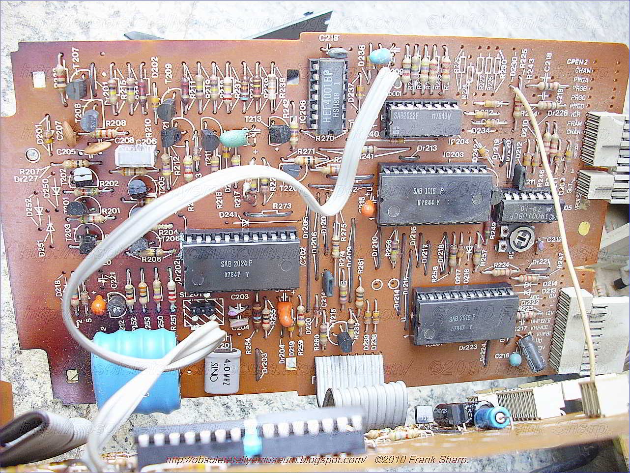
This version was featuring first time A frequency synthesized tuning system based around PHILIPS TRD chipset. (SAB2024 SAB2022 SAB1016 SAB2015 SAB3012)
SAB2015 Station search + RAM
SAB2022 TV AFT (AUTOMATIC FINE TUNING)
SAB2024 TV PLL TUNING
SAB1016 TV CHARACTER FADE IN (OSD)
SAB 3012 US/IF/REC 2X64 CODES REMOTE RECEIVER.
The present invention relates to a television set which includes a picture display device, an alpha numerical character generating circuit connected to the said device, a control device and means for checking analogue data relating to the operation of the set, such as volume, brightness and color. The system commonly used on television receivers for tuning into the required channels is the so-called FREQUENCY SYNTHESIZER system. This system, made possible by the advent of integrated circuits, offers a number of advantages over other known systems, such as the conventional potentiometer type MECHANICAL MEMORY systems and the more recent so-called VOLTAGE SYNTHESIZER systems. The frequency synthesizer system is fully electronic enabling any channel to be called up directly by the user who formulates the channel number on a keyboard or other control device. The system usually consists of a quartz-controlled reference oscillator, a phase lock loop, a programmable divider and a computer which supplies the number to be sent to the programmable divider in response to the number of the channel set by the user. Thanks to the phase lock loop, for each channel number set by the user, the frequency of the local oscillator on the set is kept so stable and accurate that the set is tuned with great precision to the corresponding channel signal.
 For further details concerning frequency synthesizer tuning systems, refer to the article entitled "A Frequency Synthesizer for Television Receivers" by E. G. Breeze, published in the November, 1974 issue of the "Transactions BTR" Magazine, or "Digital Television Tuner Uses MOS LSI and Non Volatile Memory" by L. Penner, published in the April 1, 1976 issue of "Electronics".
Channel selection is controlled by a frequency synthesizer a sweep of available channels is made by a channel selecting arrangement and this sweep is arranged to be stopped when a signal is received. When the sweeping is stopped a fine tuning arrangement takes control to respond to the frequency of the received signal and to compensate for any drift of that signal.
According to this invention there is provided a receiver comprising frequency synthesizer controlled channel selection means which includes a fine tuning arrangement; means for initiating a sweep of available channels by the channel selection means; means for stopping the sweep on reception of a signal and means, operable on cessation of sweeping and responsive to the frequency of the signal, and arranged to control the fine tuning arrangement to compensate for frequency drift of the signal.
The receiver may be in the form of a television receiver.
 The means operable a cessation of sweeping may comprise level detector means arranged to receive a signal whose level is representative of the frequency of the received signal and to provide an output signal when a predetermined frequency drift is detected.
In a preferred form two level comparators are provided each arranged to receive the frequency representative signal and a respective reference level and to provide an output respectively representative of an upward and downward frequency drift exceeding predetermined limits.
The signal whose level is representative of the frequency of the received signal may be provided by automatic frequency control (A.F.C.) means conveniently in the form of an A.F.C. discriminator.
The means operable or cessation of sweeping may be arranged to control the fine tuning arrangement via a signal path which includes means for blocking said signal path until the said signal is received.
The means for blocking may be in the form of gate means connected to the said signal path and arranged to receive a second input a signal indicative of the receipt of the said signal.
The means for initiating a sweep may comprise an operator control coupled to control input means of the channel selection means, and the means for stopping sweeping is operative to isolate the operator control from the said control input means.
The operator may be coupled to the channel selection means via gating means operative to open an operation of the operator control and the means for stopping sweeping may provide a signal operative to block the gating means or receipt of the said signal.
The means for stopping sweeping may include means for detecting the reception of the said signal which in a preferred form of television receiver comprises a sync comparator operative to compare video signals with line flyback signals and to provide an output signal whose level is indicitive of the reception of the said signal.
 The frequency synthesizer system lends itself well to a number of different modes of television channel tuning;
direct selection by formulating the required channel number as described above television channels are numbered: for example, in the European C.C.I.R. standard, V.H.F. band channels are numbered from 2 to 12 and U.H.F. band channels from 21 to 69; in the American Standard, VHF channels are numbered from 2 to 13 and UHF from 14 to 83).
memory selection: each of a certain set of keys corresponds to a preselected and memorised channel;
automatic scanning of all the channels of a given standard, or of all the channels contained in the memory or continuous scanning of all the frequency bands involved.
The first application enables immediate, direct selection of any one of the channels in the relative standard (60 in Europe, 82 in America).
the second enables faster detection of one of a limited number of preferred channels.
The third is a fast, simple way of finding out which standard channels can be received, which channels have been memorised and whether other broadcasting stations exist on non-standard frequencies such as the private broadcasting stations in Italy (there are currently over a hundred operating).
Line synch Switched Mode Power Supply with Line deflection output Transistor Drive Circuit:
 A stabilized supply voltage circuit for a picture display device comprising a chopper wherein the switching signal has the line frequency and is duration-modulated. The coil of the chopper constitutes the primary winding of a transformer a secondary winding of which drives the line output transistor so that the switching transistor of the chopper also functions as a driver for the line output stage. The oscillator generating the switching signal may be the line oscillator. In a special embodiment the driver and line output transistor conduct simultaneously and in order to limit the base current of the line output transistor a coil shunted by a diode is incorporated in the drive line of the line output transistor. Other secondary windings of the transformer drive diodes which conduct simultaneously with the efficiency diode of the chopper so as to generate further stabilized supply voltages.

Description:
The invention relates to a circuit arrangement in a picture display device wherein the input direct voltage between two input terminals, which is obtained be rectifying the mains alternating voltage, is converted into a stabilized output direct voltage by means of a switching transistor and a coil and wherein the transistor is connected to a first input terminal and an efficiency diode is connected to the junction of the transistor and the coil. The switching transistor is driven by a pulsatory voltage of line frequency which pulses are duration-modulated in order to saturate the switching transistor during part of the period dependent on the direct voltage to be stabilized and to cut off this transistor during the remaining part of the period. The pulse duration modulation is effected by means of a comparison circuit which compares the direct voltage to be stabilized with a substantially constant voltage, the coil constituting the primary winding of a transformer.
Such a circuit arrangement is known from German "Auslegeschrift" 1.293.304. wherein a circuit arrangement is described which has for its object to convert an input direct voltage which is generated between two terminals into a different direct voltage. The circuit emp
 loys a switch connected to the first terminal of the input voltage and periodically opens and closes so that the input voltage is converted into a pulsatory voltage. This pulsatory voltage is then applied to a coil. A diode is arranged between the junction of the switch and the coil and the second terminal of the input voltage whilst a load and a charge capacitor in parallel thereto are arranged between the other end of the coil and the second terminal of the input voltage. The assembly operates in accordance with the known efficiency principle i.e., the current supplied to the load flows alternately through the switch and through the diode. The function of the switch is performed by a switching transistor which is driven by a periodical pulsatory voltage which saturates this transistor for a given part of the period. Such a configuration is known under different names in the
literature; it will be referred to herein as a "chopper." A known advantage thereof, is that the switching transistor must be able to stand a high voltage or provide a great current but it need not dissipate a great power. The output voltage of the chopper is compared with a constant reference voltage. If the output voltage attempts to vary because the input voltage and/or the load varies, a voltage causing a duration modulation of the pulses is produced at the output of the comparison arrangement. As a result the quantity of the energy stored in the coil varies and the output voltage is maintained constant. In the German "Auslegeschrift" referred to it is therefore an object to provide a stabilized supply
voltage device.
 In the circuit arrangement according to the mentioned German "Auslegeschrift" the frequency of the load variations or a harmonic thereof is chosen as the frequency for the switching voltage. Particularly when the load fed by the chopper is the line deflection circuit of a picture display device, wherein thus the impedance of the load varies in the rhythm of the line frequency, the frequency of the switching voltage is equal to or is a multiple of the line frequency.
It is to be noted that the chopper need not necessarily be formed as that in the mentioned German "Auslegeschrift." In fact, it is known from literature that the efficiency diode and the coil may be exchanged. It is alternatively possible for the coil to be provided at the first terminal of the input voltage whilst the switching transistor is arranged between the other end and the second terminal of the input voltage. The efficiency diode is then provided between the junction of said end and the switching transistor and the load. It may be recognized that for all these modifications a voltage is present across the connections of the coil which voltage has the same frequency and the same shape as the pulsatory switching voltage. The control voltage of a line deflection circuit is a pulsatory voltage which causes the line output transistor to be saturates and cut off alter nately. The invention is based on the recognition that the voltage present across the connections of the coil is suitable to function as such a control voltage and that the coil constitutes the primary of a transformer. To this end the circuit arrangement according to the invention is characterized in that a secondary winding of the transformer drives the switching element which applies a line deflection current to line deflection coils and by which the voltage for the final anode of a picture display tube which forms part of the picture display device is generated, and that the ratio between the period during which the switching transistor is saturated and the entire period, i.e., the switching transistor duty cycle is between 0.3 and 0.7 during normal operation.
The invention is also based on the recognition that the duration modulation which is necessary to stabilize the supply voltage with the switching transistor does not exert influence on the driving of the line output transistor. This resides in the fact that in case of a longer or shorter cut-off period of the line output transistor the current flowing through the line deflection coils thereof is not influenced because of the efficiency diode current and transistor current are taken over or, in case of a special kind of transistor, the collector-emitter current is taken over by the base collector current and conversely. However, in that case the above-mentioned ratios of 0.3 : 0.7 should be taken into account since otherwise this take-over principle is jeopardized.
As will be further explained the use of the switching transistor as a driver for the line output transistor in an embodiment to be especially described hereinafter has the further advantage that the line output transistor automatically becomes non-conductive when this switching transistor is short circuited so that the deflection and the EHT for the display tube drop out and thus avoid damage thereof.
Due to the step according to the invention the switching transistor in the stabilized supply functions as a driver for the line deflection circuit. The circuit arrangement according to the invention may in addition be equipped with a very efficient safety circuit so that the reliability is considerably enhanced, which is described in the U.S. Pat. No. 3,629,686. The invention is
furthermore based on the recognition of the fact that the pulsatory voltage present across the connections of the coil is furthermore used and to this end the circuit arrangement according to the invention is characterized in that secondary windings of the transformer drive diodes which conduct simultaneously with the efficiency diode so as to generate further stabilized direct voltages, one end of said diodes being connected to ground.
In order that the invention may be readily carried into effect, a few embodiments thereof will now be described in detail by way of example with reference to the accompanying diagrammatic drawings in which:
FIG. 1 shows a principle circuit diagram wherein the chopper and the line deflection circuit are further shown but other circuits are not further shown.
FIGS. 2a, 2b and 2c show the variation as a function of time of two currents and of a voltage occurring in the circuit arrangement according to FIG. 1.
FIGS. 3a 3b, 3c and 3d show other embodiments of the chopper.
FIGS. 4a and 4b show modifications of part of the circuit arrangement of FIG. 1.
 In FIG. 1 the reference numeral 1 denotes a rectifier circuit which converts the mains voltage supplied thereto into a non-stabilized direct voltage. The collector of a switching transistor 2 is connected to one of the two terminals between which this direct voltage is obtained, said transistor being of the npn-type in this embodiment and the base of which receives a pulsatory voltage which originates through a control stage 4 from a modulator 5 and causes transistor 2 to be saturated and cut off alternately. The voltage waveform 3 is produced at the emitter of transistor 2. In order to maintain the output voltage of the circuit arrangement constant, the duration of the pulses provided is varied in modulator 5. A pulse oscillator 6 supplies the pulsatory voltage to modulator 5 and is synchronized by a signal of line frequency which originates from the line oscillator 6' present in the picture display device. This line oscillator 6' is in turn directly synchronized in known manner by pulses 7' of line frequency which are present in the device and originate for example from a received television signal if the picture display device is a television receiver. Pulse oscillator 6 thus generates a pulsatory voltage the repetition frequency of which is the line frequency.
 The emitter of switching transistor 2 is connected at one end to the cathode of an efficiency diode 7 whose other end is connected to the second input voltage terminal and at the other end to primary winding 8 of a transformer 9. Pulsatory voltage 3 which is produced at the cathode of efficiency diode 7 is clamped against the potential of said second terminal during the intervals when this diode conducts. During the other intervals the pulsatory voltage 3 assumes the value V i . A charge capacitor 10 and a load 11 are arranged between the other end of winding 8 and the second input voltage terminal. The elements 2,7,8,10 and 11 constitute a so-called chopper producing a direct voltage across charge capacitor 10, provided that capacitor 10 has a sufficiently great value for the line frequency and the current applied to load 11 flowing alternately through switching transistor 2 or through efficiency diode 7. The output voltage V o which is the direct voltage produced across charge capacitor 10 is applied to a comparison circuit 12 which compares the voltage V o with a reference voltage. Comparison circuit 12 generates a direct voltage which is applied to modulator 5 so that the duration of the effective period δ T of switching transistor 2 relative to the period T of pulses 3 varies as a function of the variations of output voltage V 0 . In fact, it is readily evident that output voltage V o is proportional to the ratio δ :
V o = V i . δ
Load 11 of the chopper consists in the consumption of parts of the picture display device which are fed by output voltage V 0 . In a practical embodiment of the circuit arrangement according to FIG. 1 wherein the mains alternating voltage has a nominal effective value of 220 V and the rectified voltage V i is approximately 270 V, output voltage V o for δ = 0.5 is approximately 135 V. This makes it also possible, for example, to feed a line deflection circuit as is shown in FIG. 1 wherein load 11 then represents different parts which are fed by the chopper. Since voltage V o is maintained constant due to pulse duration modulation, the supply voltage of this line deflection circuit remains constant with the favorable result that the line amplitude(= the width of the picture displayed on the screen of the picture display tube) likewise remains constant as well as the EHT required for the final anode of the picture display tube in the same circuit arrangement independent of the variations in the mains voltage and the load on the EHT generator (= variations in brightness).
However, variations in the line amplitude and the EHT may occur as a result of an insufficiently small internal impedance of the EHT generator. Compensation means are known for this purpose. A possibility within the scope of the present invention is to use comparison circuit 12 for this purpose. In fact, if the beam current passes through an element having a substantially quadratic characteristic, for example, a voltage-dependent resistor, then a variation for voltage V o may be obtained through comparison circuit 12 which variation is proportional to the root of the variation in the EHT which is a known condition for the line amplitude to remain constant.
In addition this facilitates smoothing of voltage V o since the repetition frequency of pulsatory voltage 3 is many times higher than that of the mains and a comparatively small value may be sufficient for charge capacitor 10. If charge capacitor 10 has a sufficiently high value for the line frequency, voltage V o is indeed a direct voltage so that a voltage having the same form as pulsatory voltage 3 is produced across the terminals of primary winding 8. Thus voltages which have the same shape as pulsatory voltage 3 but have a greater or smaller amplitude are produced across secondary windings 13, 14 of transformer 9 (FIG. 1 shows only 2 secondary windings but there may be more). The invention is based on the recognition that one end of each secondary winding is connected to earth while the other end thereof drives a diode, the winding sense of each winding and the direction of conductance of each diode being chosen to be such that these diodes conduct during the same period as does efficiency diode 7. After smoothing, stabilized supply voltages, for example, at terminal 15 are generated in this manner at the amplitudes and polarities required for the circuit arrangements present in the picture display device. In FIG. 1 the voltage generated at terminal 15 is, for example, positive relative to earth. It is to be noted that the load currents of the supply voltages obtained in this manner cause a reduction of the switching power which is economized by efficiency diode 7. The sum of all diode currents including that of diode 7 is in fact equal to the current which would flow through diode 7 if no secondary winding were wound on transformer 9 and if no simultaneous diode were used. This reduction may be considered an additional advantage of the circuit arrangement according to the invention, for a diode suitable for smaller powers may then be used. However, it will be evident that the overall secondary load must not exceed the primary load since otherwise there is the risk of efficiency diode 7 being blocked so that stabilization of the secondary supply voltages would be out of the question.
 It is to be noted that a parabola voltage of line frequency as shown at 28 is produced across the charge capacitor 10 if this capacitor is given a smaller capacitance so that consequently the so-called S-correction is established.
In FIG. 1 charge capacitors are arranged between terminals 15 etc. and earth so as to ensure that the voltages on these points are stabilized direct voltages. If in addition the mean value of the voltage on one of these terminals has been made equal to the effective value of the alternating voltage which is required for heating the filament of the picture display tube present in the picture display device, this voltage is suitable for this heating. This is a further advantage of the invention since the cheap generation of a stabilized filament voltage for the picture display tube has always been a difficult problem in transistorized arrangements.
A further advantage of the picture display device according to the invention is that transformer 9 can function as a separation transformer so that the different secondary windings can be separated from the mains and their lower ends can be connected to ground of the picture display device. The latter step makes it possible to connect a different apparatus such as, for example, a magnetic recording and/or playback apparatus to the picture display device without earth connection problems occurring.
In FIG. 1 the reference numeral 14 denotes a secondary winding of transformer 9 which in accordance with the previously mentioned recognition of the invention can drive line output transistor 16 of the line deflection circuit 17. Line deflection circuit 17 which is shown in a simplified form in FIG. 1 includes inter alia line deflection coils 18 and an EHT transformer 19 a secondary winding 20 of which serves for generating the EHT required for the acceleration anode of the picture display tube. Line deflection circuit 17 is fed by the output voltage V o of the chopper which voltage is stabilized due to the pulse duration modulation with all previously mentioned advantages. Line deflection circuit 17 corresponds, for example, to similar arrangements which have been described in U.S. Pat. No. 3,504,224 issued Mar. 31, 1970 to J.J. Reichgelt et al., U.S. patent application Ser. No. 737,009 filed June 14, 1968 by W. H. Hetterscheid and U.S. application Ser. No. 26,497 filed April 8, 1970 by W. Hetterscheid et al. It will be evident that differently formed lined deflection circuits are alternatively possible.
It will now be shown that secondary winding 14 can indeed drive a line deflection circuit so that switching transistor 2 can function as a driver for the line deflection. FIGS. 2a and b show the variation as a function of time of the current i C which flows in the collector of transistor 16 and of the drive voltage v 14 across the terminals of secondary winding 14. During the flyback period (0, t 1 ) transistor 16 must be fully cut off because a high voltage peak is then produced at its collector; voltage v 14 must then be absolutely negative. During the scan period (t 1 , t 4 ) a sawtooth current i C flows through the collector electrode of transistor 16 which current is first negative and then changes its direction. As the circuit arrangement is not free from loss, the instant t 3 when current i C becomes zero lies, as is known, before the middle of the scan period. At the end t 4 of the scan period transistor 16 must be switched off again. However, since transistor 16 is saturated during the scan period and since this transistor must be suitable for high voltages and great powers so that its collector layer is thick, this transistor has a very great excess of charge carriers in both its base and collector layers. The removal of these charge carriers takes a period t s which is not negligible whereafter the transistor is indeed switched off. Thus the fraction δ T of the line period T at which v 14 is positive must end at the latest at the instant (t 4 - t s ) located after the commencement (t = 0) of the previous flyback.
 The time δ T may be initiated at any instant t 2 which is located between the end t 1 of the flyback period and the instant t 3 when collector current i C reverses its direction. It is true that emitter current flows through transistor 16 at the instant t 2 , but collector current i C is not influenced thereby, at least not when the supply voltage (= V o ) for line deflection circuit 17 is high enough. All this has been described in the U.S. Pat. No. 3,504,224. The same applies to line deflection circuits wherein the collector base diode does not function as an efficiency diode as is the case in the described circuit 17, but wherein an efficiency diode is arranged between collector and emitter of the line output transistor. In such a case the negative part of the current i C of FIG. 2a represents the current flowing through the said efficiency diode.
 After the instant t 3 voltage v 14 must be positive. In other words, the minimum duration of the period T when voltage v 14 must be positive is (t 4 - t s ) - t 3 whilst the maximum duration thereof is (t 4 - t s ) - t 1 . In a television system employing 625 lines per raster the line period t 4 is approximately 64 μus and the flyback period is approximately 12 μus. Without losses in the circuit arrangement instant t 3 would be located approximately 26 μus after the instant t 1 , and with losses a reasonable value is 22 μus which is 34 μus after the commencement of the period. If for safety's sake it is assumed that t s lasts approximately 10 μus, the extreme values of δ T are approximately 20 and 42 μus and consequently the values for δ are approximately 0.31 and 0.66 at a mean value which is equal to approximately 0.49. It was previously stated that a mean value of δ = 0.5 was suitable. Line deflection circuit 17 can therefore indeed be used in combination with the chopper in the manner described, and the relative variation of δ may be (0.66 - 0.31) : 0.49 = 71.5 percent. This is more than necessary to obviate the variations in the mains voltage or in the various loads and to establish the East-West modulation and ripple compensation to be described hereinafter. In fact, if it is assumed that the mains voltage varies between -15 and +10 percent of the nominal value of 220 V, while the 50 Hz ripple voltage which is superimposed on the input voltage V i has a peak-to-peak value of 40 V and V i is nominally 270 V, then the lowest occurring V i is:
0.85 × 270 V - 20 V = 210 V and the highest occurring V i is
1.1 × 270 V + 20 V = 320 V. For an output voltage V o of 135 V the ratio must thus vary between
δ = 135 : 210 = 0.64 and δ = 135 : 320 = 0.42.
A considerable problem presenting itself is that of the simultaneous or non-simultaneous drive of line output transistor 16 with switching transistor 2, it being understood that in case of simultaneous drive both transistors are simultaneously bottomed, that is during the period δ T. This depends on the winding sense of secondary winding 14 relative to that of primary winding 8. In FIG. 1 it has been assumed that the drive takes place simultaneously so that the voltage present across winding 14 has the shape shown in FIG. 2b. This voltage assumes the value n(V i - V o ) in the period δ T and the value -nVo in the period (1 - δ )T, wherein n is the ratio of the number of turns on windings 14 and 8 and wherein V o is maintained constant at nominal mains voltage V o = δ V inom . However, if as a result of an increase or a decrease of the mains voltage V i increases or decreases proportionally therewith, i.e., V i = V i nom + Δ V, the positive portion of V 14 becomes equal to n(V i nom - V o +Δ V) = n [(1 -δ)V i nom +ΔV] = n(0.5 V inom +ΔV) if δ = 0.5 for V i = V i nom. Relatively, this is a variation which is twice as great. For example, if V i nom = 270 V and V o = 135 V, a variation in the mains voltage of from -15 to +10 percent causes a variation of V i of from -40.5 V to +27 V which ranges from -30 to +20 percent of 135 V which is present across winding 8 during the period δ T. The result is that transistor 16 can always be bottomed over a large range of variation. If the signal of FIG. 2b would be applied through a resistor to the base of transistor 16, the base current thereof would have to undergo the same variation while the transistor would already be saturated in case of too low a voltage. In this case it is assumed that transformer 9 is ideal (without loss) and that coil 21 has a small inductance as is explained in the U.S. patent application Ser. No. 737,009 above mentioned. It is therefore found to be desirable to limit the base current of transistor 16.
This may be effected by providing a coil 22 having a large value inductance, approximately 100 μH, between winding 14 and the small coil 21. The variation of said base current i b is shown in FIG. 2c but not to the same scale as the collector current of FIG. 2a. During the conducting interval δ T current i b varies as a linear function of time having a final value of wherein L represents the inductance of coil 22. This not only provides the advantage that this final value is not immediately reached, but it can be shown that variation of this final value as a function of the mains voltage has been reduced, for there applies at nominal mains voltage that: If the mains voltage V i = V i nom +Δ V, then ##SPC1## because V i nom = 2 V o . Thus this variation is equal to that of the mains voltage and is not twice as great.
 During switching off, t 2 , of transistor 16 coil 22 must exert no influence and coil 21 must exert influence which is achieved by arranging a diode 23 parallel to coil 22. Furthermore the control circuit of transistor 16 in this example comprises the two diodes 24 and 25 as described in U.S. application Ser. No. 26,497 above referred to, wherein one of these diodes, diode 25 in FIG. 1, must be shunted by a resistor.
The control circuit of transistor 16 may alternatively be formed as is shown in FIG. 4. In fact, it is known that coil 21 may be replaced by the parallel arrangement of a diode 21' and a resistor 21" by which the inverse current can be limited. To separate the path of the inverse current from that of the forward current the parallel arrangement of a the diode 29' and a resistor 29" must then be present. This leads to the circuit arrangement shown in the upper part of FIG. 4. This circuit arrangement may now be simplified if it is noted that diodes 25 and 21' on the one hand and diodes 23 and 29' on the other hand are series-arranged. The result is shown in the lower part of FIG. 4 which, as compared with the circuit arrangement of FIG. 1, employs one coil less and an additional resistor.
FIG. 3 shows possible modifications of the chopper. FIG. 3a shown in a simplified form the circuit arrangement according to FIG. 1 wherein the pulsatory voltage present across the connections of windings 8 has a peak-to-peak amplitude of V i - V o = 0.5 V i for δ = 0.5, As has been stated, the provision of coil 22 gives a relative variation for the base current of transistor 16 which is equal to that of the mains voltage. In the cases according to FIG. 3b, 3c and 3d the peak-to-peak amplitude of the voltage across winding 8 is equal to V i so that the provision of coil 22 results in a relative variation which is equal to half that of the mains voltage which is still more favorable than in the first case.
Transistors of the npn type are used in FIG. 3. If transistors of the pnp type are used, the relevant efficiency diodes must of course be reversed.
In this connection it is to be noted that it is possible to obtain an output voltage V o with the aid of the modifications according to FIGS. 3b, c and d, which voltage is higher than input voltage V i . These modifications may be used in countries such as, for example, the United of America or France where the nominal mains voltage is 117 or 110 V without having to modify the rest of the circuit arrangement.
The above-mentioned remark regarding the sum of the diode currents only applies, however, for the modifications shown in FIGS. 3a and d.
If line output transistor 16 is not simultaneously driven with switching transistor 2, efficiency diodes 7 conducts simultaneously with transistor 16 i.e., during the period which is denoted by δ T in FIGS. 1 and 2b. During that period the output voltage V o of the chopper is stabilized so that the base current of transistor 16 is stabilized without further difficulty. However, a considerable drawback occurs. In FIG. 1 the reference numeral 26 denotes a safety circuit the purpose of which is to safeguard switching transistor 2 when the current supplied to load 11 and/or line deflection circuit 17 becomes to high, which happens because the chopper stops. After a given period output voltage V o is built up again, but gradually which means that the ratio δ is initially small in the order of 0.1. All this is described in U.S. patent No. 3,629,686. The same phenomenon occurs when the display device is switched on. Since δ = 0.1 corresponds to approximately 6 μs when T = 64 μs, efficiency diode 7 conducts in that case for 64 - 6 = 58 μus so that transistor 16 is already switched on at the end of the scan or at a slightly greater ratio δ during the flyback. This would cause an inadmissibly high dissipation. For this reason the simultaneous drive is therefore to be preferred.
The line deflection circuit itself is also safeguarded: in fact, if something goes wrong in the supply, the driver voltage of the line deflection circuit drops out because the switching voltage across the terminals of primary winding 8 is no longer present so that the deflection stops. This particularly happens when switching transistor 2 starts to constitute a short-circuit between emitter and collector with the result that the supply voltage V o for the line deflection circuit in the case of FIG. 1 becomes higher, namely equal to V i . However, the line output transformer is now cut off and is therefore also safe as well as the picture display tube and other parts of the display device which are fed by terminal 15 or the like. However, this only applies to the circuit arrangement according to FIG. 1 or 3a.
 Pulse oscillator 6 applies pulses of line frequency to modulator 5. It may be advantageous to have two line frequency generators as already described, to wit pulse oscillator 6 and line oscillator 6' which is present in the picture display device and which is directly synchronized in known manner by line synchronizing pulses 7'. In fact, in this case line oscillator 6' applies a signal of great amplitude and free from interference to pulse oscillator 6. However, it is alternatively possible to combine pulse oscillator 6 and line oscillator 6' in one single oscillator 6" (see FIG. 1) which results in an economy of components. It will be evident that line oscillator 6' and oscillator 6" may alternatively be synchronized indirectly, for example, by means of a phase discriminator. It is to be noted neither pulse oscillator 6, line oscillator 6' and oscillator 6" nor modulator 5 can be fed by the supply described since output voltage V o is still not present when the mains voltage is switched on. Said circuit arrangements must therefore be fed directly from the input terminals. If as described above these circuit arrangements are to be separated from the mains, a small separation transformer can be used whose primary winding is connected between the mains voltage terminals and whose secondary winding is connected to ground at one end and controls a rectifier at the other end.
Capacitor 27 is arranged parallel to efficiency diode 7 so as to reduce the dissipation in switching transistor 2. In fact, if transistor 2 is switched off by the pulsatory control voltage, its collector current decreases and its collector-emitter voltage increases simultaneously so that the dissipated power is not negligible before the collector current has becomes zero. If efficiency diode 7 is shunted by capacitor 27 the increase of the collector-emitter voltage is delayed i.e., this voltage does not assume high values until the collector current has already been reduced. It is true that in that case the dissipation in transistor 2 slightly increases when it is switched on by the pulsatory control voltage but on the other hand since the current flowing through diode 7 has decreased due to the presence of the secondary windings, its inverse current is also reduced when transistor 2 is switched on and hence its dissipation has become smaller.
In addition it is advantageous to delay these switching-on and switching-off periods to a slight extent because the switching pulses then contain fewer Fourier components of high frequency which may cause interferences in the picture display device and which may give rise to visible interferences on the screen of the display tube. These interferences occupy a fixed position on the displayed image because the switching frequency is the line frequency which is less disturbing to the viewer. In a practical circuit wherein the line frequency is 15,625 Hz and wherein switching transistor 2 is an experimental type suitable for a maximum of 350 V collector-emitter voltage or 1 A collector current and wherein efficiency diode 7 is of the Philips type BA 148 the capacitance of capacitor 27 is approximately 680 pF whilst the load is 70 W on the primary and 20 W on the secondary side of transformer 9. The collector dissipation upon switching off is 0.3 W (2.5 times smaller than without capacitor 27) and 0.7 W upon switching on.
 As is known the so-called pincushion distortion is produced in the picture display tubes having a substantially flat screen and large deflection angles which are currently used. This distortion is especially a problem in color television wherein a raster correction cannot be brought about by magnetic means. The correction of the so-called East-West pincushion distortion i.e., in the horizontal direction on the screen of the picture display tube can be established in an elegant manner with the aid of the circuit arrangement according to the invention. In fact, if the voltage generated by comparison circuit 12 and being applied to modulator 5 for duration-modulating pulsatory voltage 3 is modulated by a parabola voltage 28 of field frequency, pulsatory voltage 3 is also modulated thereby. If the power consumption of the line deflection circuit forms part of the load on the output voltage of the chopper, the signal applied to the line deflection coils is likewise modulated in the same manner. Conditions therefore are that the parabola voltage 28 of field frequency has a polarity such that the envelope of the sawtooth current of line frequency flowing through the line deflection coils has a maximum in the middle of the scan of the field period and that charge capacitor 10 has not too small an impedance for the field frequency. On the other hand the other supply voltages which are generated by the circuit arrangement according to the invention and which might be hampered by this component of field frequency must be smoothed satisfactorily.
A practical embodiment of the described example with the reference numerals given provides an output for the supply of approximately 85 percent at a total load of 90 W, the internal resistance for direct current loads being 1.5 ohms and for pulsatory currents being approximately 10 ohms. In case of a variation of ± 10 percent of the mains voltage, output voltage V o is stable within 0.4 V. Under the nominal circumstances the collector dissipation of switching transistor 2 is approximately 2.5 W.
Since the internal resistance of the supply is so small, it can be used advantageously, for example, at terminal 15 for supplying a class-B audio amplifier which forms part of the display device. Such an amplifier has the known advantages that its dissipation is directly proportional to the amplitude of the sound to be reproduced and that its output is higher than that of a class-A amplifier. On the other hand a class-A amplifier consumes a substantially constant power so that the internal resistance of the supply voltage source is of little importance. However, if this source is highly resistive, the supply voltage is modulated in the case of a class-B amplifier by the audio information when the sound intensity is great which may detrimentally influence other parts of the display device. This drawback is prevented by means of the supply according to the invention.
The 50 Hz ripple voltage which is superimposed on the rectified input voltage V i is compensated by comparison circuit 12 and modulator 5 since this ripple voltage may be considered to be a variation of input voltage V i . A further compensation is obtained by applying a portion of this ripple voltage with suitable polarity to comparison circuit 12. It is then sufficient to have a lower value for the smoothing capacitor which forms part of rectifier circuit 1 (see FIG. 3). The parabola voltage 28 of field frequency originating from the field time base is applied to the same circuit 12 so as to correct the East-West pincushion distortion.


F UNIT Luminance and chromince unit TDA2560 TDA2527.
H UNIT HORIZONTAL OSC TDA2590
G UNIT RGB AMPL MATRIX TDA2530
E UNIT SOUND UNIT TDA1039
I UNIT FRAME TDA1270
M UNIT SUPPLY CONTROL TDA2640.
A UNIT MAINS RECT.
Control circuit for a switched-mode power supply, particularly for a television receiver: VOXSON T5647CD CHASSIS CT4 20AX SWITCH MODE POWER SUPPLY.
The Control UNIT is developed around the PHILIPS TDA2640.
"Television Switched-Mode Power Supply Using the TDA2640", Mullard Technical Communications, L. M. White, pp. 258-279, Jul. 1975.
A switched-mode power supply provided with a control stage and a switching stage coupled by means of a transformer. The collector of an additional transistor is connected to the transformer. In this manner the ratio of the collector current to the base current of the switching transistor can assume a predetermined value, for example a constant value whatever the value of the mains voltage applied to the power supply.
This type of switched-mode power supply is used more and more because of the numerous advantages it presents as regards energy efficiency, reliability, compactness, etc. However, as for the majority of the other types of power supplies, its operation on mains supplies of different voltages imposes the use of either a transformer with taps or switch-over from full wave rectification at the highest mains voltage to a voltage doubler rectification for the lowest mains voltage.
It is known that the specific qualities of a switched-mode power supply depend for a large part on the switching speed of the switching transistor at the moment at which the latter passes periodically from the conductive state to the blocking state; this speed is at its maximum when the switching transistor presents, at the turn-off moment, a certain ratio between the collector current and the base current IC/IB: if this ratio is too low, the delay in the recombination of the charges stored in the base increases the switching time; if it is too high there is the risk that the transistor is brought out of saturation before it is blocked, which results in its substantially immediate destruction. For the known switched-mode power supplies it is not possible to maintain a suitable IC/IB ratio in the presence of large variations of the non-regulated rectified DC voltage which result from the connection to the nominal mains voltages of, for example, 110 or 220 V; actually, if the variations in IB are substantially proportional to the variations in the non-regulated voltage, the same does not happen for those of the IC whose amplitude is less.
However, the importance of having a power supply which can operate without any switching on mains supplies of 110 or 220 V is evident: for the manufacturer it is cheaper to produce and the reliability is increased; while the user does not run the risk of incorrect manipulations, particularly when the power supply is destined for use in portable television sets.
One of the objects of the invention is to realize a control circuit which permits the switched-mode power supply to operate without switching in conditions which are substantially optimum and in the presence of mains voltage variations in the range of 90 to 250 Volts.
A further object of the invention is to ensure that said IC/IB ratio of the switching transistor has a predetermined and, more particularly a constant value at the turn-off moment whatever the value of the mains voltage applied to the power supply.
The control circuit according to the invention is characterized in that the end of the primary winding of the first transformer not connected to the driver transistor is connected to the collector of an additional transistor whose emitter is coupled with the non-regulated direct voltage source. Advantageously it is characterized in that the emitter of the additional transistor is connected to one end of a resistor, the other end of this resistor being connected to a constant current source, and that the constant current source is constituted by a second additional transistor, the two additional transistors being of complementary conductivity and their emitters being connected with each other through a resistor, whilst the collector of the second additional transistor is connected to one of the poles of the non-regulated rectified direct voltage source and the collector of the first additional transistor is connected to the end of the primary winding of the first transformer not connected to the driver transistor.
Whilst combining the action of a ballast transistor with that of a variable current generator, the circuit according to the invention thus maintains automatically a desired IC/IB ratio of the switching transistor whatever the value of the mains voltage applied to the power supply.
TDA2590 horizontal oscillator combination
GENERAL DESCRIPTION
— The TDA2590 is a monolithic integrated circuit designed
as a horizontal oscillator combination for TV receivers and monitors.

It is constructed using the Fairchild Planar* process.
LINE OSCILLATOR USING THE THRESHOLD SWITCHING PRINCIPLE
PHASE COMPARISON BETWEEN SYNC PULSE AND OSCILLATOR VOLTAGE (d>1)
PHASE COMPARISON BETWEEN LINE FLYBACK PULSE AND OSCILLATOR VOLTAGE
(<62) Y
SWITCH FOR CHANGING THE FILTER CHARACTERISTIC AND THE GATE CIRCUIT
{WHEN USED FOR VCR)
COINCIDENCE DETECTOR (¢3)
SYNC SEPARATOR
NOISE SEPARATOR
VERTICAL SYNC SEPARATOR AND OUTPUT STAGE
COLOR BURST KEYING AND LINE FLYBACK BLANKING PULSE GENERATOR
PHASE SHIFTER FOR THE OUTPUT PULSE
OUTPUT PULSE DURATION SWITCHING
OUTPUT STAGE FOR DIRECT DRIVE OF THYRISTOR DEFLECTION CIRCUITS
SYNC GATING PULSE GENERATOR
LOW SUPPLY VOLTAGE PROTECTION.
VOXSON T5647CD CHASSIS CT4 20AX Television set which displays analog data relevant to the operation of the television set on its video display:
(SAB2024 SAB2022 SAB1016 SAB2015 SAB3012)
SAB2015 Station search + RAM
SAB2022 TV AFT (AUTOMATIC FINE TUNING)
SAB2024 TV PLL TUNING
SAB1016 TV CHARACTER FADE IN (OSD)
SAB 3012 US/IF/REC 2X64 CODES REMOTE RECEIVER.
The present invention relates to a television set which includes a picture display device, an alpha numerical character generating circuit connected to said device, a control device, means for determining analogue data relating to the operation of the set, such as volume, brightness and color, and means for displaying on said display device a combination of alpha numerical characters, supplied by said character generating device, indicating the values of said analogue data.
A control keyboard has six keys "V+", "V-", "L+", "L-", "C+" and "C-". The output of the keyboard is connected to a processing unit which is connected via a digital to analogue converter and switch to an alpha numerical character generator which is connected to a picture display device. When one of the six keys is pressed a combination of signals proportional to the analogue signal level of volume, brightness and color (V, L, C) is displayed on the picture display device. If one of the + keys is pressed, the corresponding analogue level is increased by 1/64 of maximum value, while a similar decrease is obtained by pressing one of the - keys.
1. A television set, comprising:
a picture display device for displaying a video picture;
character generator means for generating signals representative of alphabetical, numerical and/or abstract characters;
said picture display device receiving said signals and displaying the alphabetical, numerical and/or abstract characters represented thereby; and
control means for determining the value of analog data, other than the tuning frequency of said television set, relating to the operation of said television set, and for causing said character generator means to generate signals representative of alphabetical, numerical and/or abstract characters which indicate said value of said analog data.
An integrated circuit for a programmable television receiver comprises a memory for storing a plurality of programs, a digital clock and a character generating circuit for generating character signals for displaying the programs in the memory and/or time of the digital clock on the screen of a television receiver. The integrated circuit uses dynamic circuits to reduce the number of elements required, and CMOS transistors to attain a lower power dissipation. 2. A television set, comprising:
a picture display device for displaying a video picture;
character generator means for generating signals representative of alphabetical, numerical and/or abstract characters;
said picture display device receiving said signals and displaying the alphabetical, numerical and/or abstract characters represented thereby; and
control means for determining the value of analog data relating to the operation of said television set and for causing said character generator means to generate signals representative of alphabetical, numerical and/or abstract characters which indicate said value of said analog data, said control means also causing said character generator means to generate signals representative of alphabetical, numerical and/or abstract characters indicative of which of said data the user of said television set has last selected to adjust.
3. A television set, comprising:
a picture display device for displaying a video picture;
1. An integrated circuit for use in a programmable television receiver comprising:
an oscillator to which a quartz crystal is to be externally coupled;
a digital clock coupled to said oscillator;
a memory for storing a plurality of programs each including time data and associated channel data and having a plurality of recirculating dynamic shift registers each adapted to store one program;
a character generating circuit coupled to said memory and adapted to generate character signals to permit the content of said memory to be displayed on the screen of a cathode ray tube of a television receiver;
circuit means coupled to the output of said oscillator to generate shift pulses for driving said recirculating dynamic shift registers in said memory;
time comparision means coupled to the outputs of said memory and said digital clock for comparing the time data in said memory and the time of said digital clock;
means to readout said channel data from said memory; and
means responsive to said time comparing means and said readout means to form a program execution output based on said channel data when a coincidence occurs between the time data in said memory and the time of said digital clock.
2. An integrated circuit according to claim 1, in which said character generating circuit comprises:
an input for receiving horizontal timing pulses which synchronize with horizontal synchronizing pulses of the television receiver, have a frequency higher than that of the horizontal synchronizing pulse and provide a unit length in displaying characters in the horizontal direction of the cathode ray tube;
a horizontal component pulse generating circuit responsive to the horizontal timing pulses for generating horizontal component pulses which provide horizontal components of each character and have a horizontal one-digit display period, and clock pulses having the horizontal one-digit display period;
a horizontal display digit designation pulse generating circuit connected to said horizontal component pulse generating circuit to generate horizontal display digit designation pulses in response to the clock pulses;
a vertical component pulse generating circuit for generating vertical component pulses which provide vertical components of each character in response to the horizontal synchronizng pulse in the television receiver;
a multiplexer connected to said memory and said horizontal display digit designation pulse generating circuit to deliver hour data, minute data and channel data in the binary form from said memory in a predetermined sequence in response to said horizontal display digit designation pulses;
segment decoders for decoding the outputs of said multiplexer and generating segment outputs; and
output circuit means for generating character signals during each horizontal one-digit display period in response to the outputs of said segment decoders, said horizontal components pulses and said vertical component pulses.
3. An integrated circuit according to claim 2, in which said multiplexer includes a plurality of series-connected circuits each having a plurality of first MOS transistors of first channel type connected between each bit output of said multiplexer and a first potential point, the gate of one MOS transistor in each series circuit being connected to receive a binary signal having the same weight of each data and the gates of the remaining MOS transistors in each series circuit being connected to receive display digit designation pulses from said display digit designation pulse generating circuit; and a second MOS transistor of second channel type connected between the bit output and a second potential point, the gate of said second MOS transistor being connected to receive one clock pulse from said digit designation pulse generating circuit. 4. An integrated circuit according to claim 2, in which said segment decoders each include a plurality of first MOS transistors of first channel type connected between a decoder output and a first potential point, the gates of said first MOS transistors being connected to receive respective outputs of said multiplexer, and said output circuit means includes a second MOS transistor of the first channel type connected between a circuit point and each output of those segment decoders corresponding to the same horizontal component of the character and having a gate connected to receive from said vertical component pulse generating circuit a vertical component pulse associated with the horizontal component, a third MOS transistor of a second channel type connected between said circuit point and a second potential point and having a gate connected to receive one clock pulse from said display digit designation pulse generating circuit, a CMOS clocked inverter connected to said circuit point and adapted to be driven by clock pulses from said display digit designation pulse generating circuit which are different in phase from the clock pulse applied to the gate of said third transistor, and logic circuit means for gating the output of said clocked inverter in response to the corresponding horizontal component pulse. 5. An integrated circuit according to claim 1, in which said memory and digital clock are connected to a first power source line and said character generating circuit is connected to a second power source line.
A programmable TV receiver capable of preliminarily setting the time and channel number of a desired television program has recently been developed. In this case, the television receiver is automatically switched ON and OFF when a programmed time comes. Most of such programmable TV receivers use a mechanically operated clock and memory and have the drawbacks that only a lesser number of programs can be memorized. The use of the electronic memory and digital electronic clock leads to a prominent increase in the number of storable programs and also provides an accurate counting of time. The use of electronic devices permits a stored content (time and channel number) to be displayed on the screen of CRT of a TV set. When such electronic memory and electronic digital clock are realized by discrete elements, a programming device is made bulkier, incurring a high cost. In order to attain miniaturization of the device at low cost the adoption of integrated circuit is considered. However, problem arises from the standpoint of a restricted chip size when all the circuits necessary for a programmable device is integrated into an integrated circuit.
In an electronic programmable device it is necessary to prevent the content of the memory and of the digital clock from being erased when an AC power source is turned OFF. In order to prevent such a situation, switching must be effected from the power source to a dry cell. In this case, the power consumption of the programmable device must be restricted.
It is accordingly the object of this invention to provide a CMOS integrated circuit which has a low power dissipation and incorporates a memory, digital clock, character generating circuit, etc., necessary for a programmable television receiver in a chip of practical size.
According to this invention there is provided an integrated circuit for use in a programmable television receiver comprising an oscillator to which a quartz crystal is to be externally coupled; a digital clock coupled to said oscillator; a memory adapted to store a plurality of programs each including a time data and a channel data and having a plurality of recirculating dynamic shift registers each for storing one program; a character generating circuit coupled to said memory and adapted to generate character signals to permit the content of said memory to be displayed on the screen of a cathode ray tube of a television receiver; circuit means coupled to the output of said oscillator to generate shift pulses for driving said recirculating dynamic shift registers in said memory; time comparison means coupled to the outputs of said memory and said digital clock for comparing the time data in said memory and the time of said digital clock; and means responsive to said time comparing means to form a program execution output when a coincidence occurs between the time data in said memory and the time of said digital clock.
This invention can be more fully understood from the following detailed description when taken in conjunction with the accompanying drawings, in which:
character generator means for generating signals representative of alphabetical, numerical and/or abstract characters;
said picture display device receiving said signals and displaying the alphabetical, numerical, and/or abstract characters represented thereby; and
control means for determining the value of analog data relating to the operation of said television set and for causing said character generator means to generate signals representative of alphabetical, numerical and/or abstract characters which indicate said value of said analog data, said alphabetical, numerical and/or abstract characters consisting of a number of characters proportional to the value of said analog data.
4. A television set, comprising:
a picture display device for displaying a video picture;
character generator means for generating signals representative of alphabetical, numerical and/or abstract characters;
said picture display device receiving said signals and displaying the alphabetical, numerical and/or abstract characters represented thereby; and
control means for determining the value of analog data relating to the operation of said television set and for causing said character generator means to generate signals representative of alphabetical, numerical and/or abstract characters which indicate said value of said analog data, at least one of said alphabetical, numerical andl/or abstract characters indicating the type of data concerned.
5. A television set as claimed in claim 2, wherein said visual indication of which of said data the user has last selected to adjust includes a given additional character alongside said data the user has selected to adjust. 6. A television set as claimed in claim 2, wherein said visual indication of which of said data the user has last selected to adjust includes a given color for the data the user has selected to adjust. 7. A television set as claimed in claim 1, wherein said control means includes a push-button panel for generating digital electronic signals, in response to actuation thereof by the user of said television set, which instructs said control means to change the value of said analog data, said control means also causing said character generator means to generate signals representative of alphabetical, numerical and/or abstract characters which indicate the value of said adjusted analog data and also indicate that said analog data has been adjusted. 8. A television set as claimed in claim 7, wherein said control means generates digital electronic signals indicative of said adjusted value of said analog data, said control means further including a digital to analog converter for converting said digital signal into an analog signal, and a signal switch controlled by said control means for applying said analog signal to that portion of said television circuit which will cause the value of said analog data to assume said adjusted value. 9. A television set as claimed in any one of claims 1-6, additionally comprising a memory for memorizing values of said analog data. 10. A television set as claimed in claim 9, wherein the television set includes a tuning arrangement, capable of memory selection in which each of a series of keys is associated with a preselected and memorised television channel, and a memory circuit capable of memorising, for each of the said channels, number signals representing the preselected values of the said analog data. 11. A television set as claimed in any one of claims 1-6, additionally comprising means for producing an alarm when the said combination of alphabetical, numerical and/or abstract characters coincides with one or more preset combinations.
Other References:
Olson et al., "The Practical Application of On-Screen Display to a Television Receiver", IEEE Transactions on Broadcast and TV Receivers, _Aug. 1973, pp. 169-175.
Walker, "For TV Tuners a Digital Look", Electronics, Jun. 26, 1975, pp. 65-66.
Evans et al., "Direct Address Television Tuning and Display System Using Digital MOS Large Scale Integration", IEEE Transactions on Consumer Electronics, vol. CE-22, No. 4, pp. 267-288, Nov. 1976.
Electronics, vol. 48, No. 24, Nov. 27, 1975, "Philips TV Set Indicates Station Tuning and Color Settings on Screen", pp. 6E and 8E.
Werner, "Linear Color Bar Display for CTV Sets", Radio Mentor Electronic, vol. 41, No. 9, pp. 350-351, Sep. 1975.
VOXSON T5647CD CHASSIS CT4 20AX TDA1170 vertical deflection FRAME DEFLECTION INTEGRATED CIRCUIT
GENERAL DESCRIPTION f The TDA1170 and TDA1270 are monolithic integrated
circuits designed for use in TV vertical deflection systems. They are manufactured using
the Fairchild Planar* process.
Both devices are supplied in the 12-pin plastic power package with the heat sink fins bent
for insertion into the printed circuit board.
The TDA1170 is designed primarily for large and small screen black and white TV
receivers and industrial TV monitors. The TDA1270 is designed primarily for driving
complementary vertical deflection output stages in color TV receivers and industrial
monitors.
APPLICATION INFORMATION (TDA1170)
The vertical oscillator is directly synchronized by the sync pulses (positive or negative); therefore its free
running frequency must be lower than the sync frequency. The use of current feedback causes the yoke
current to be independent of yoke resistance variations due to thermal effects, Therefore no thermistor is
required in series with the yoke. The flyback generator applies a voltage, about twice the supply voltage, to
the yoke. This produces a short flyback time together with a high useful power to dissipated power
ratio.
1. A transformerless output vertical deflection circuit, comprising a vertical oscillator circuit for generating a vertical pulse train in response to vertical synchronizing pulses applied thereto, a sawtooth signal generator for generating a series of sawtooth signals, each cycle of said sawtooth signal including a pulse component, a vertical output circuit coupled to said sawtooth generator for amplifying said sawtooth signal including said pulse component and loading a vertical deflection coil, and stabilizing means connected between said vertical oscillator and said sawtooth signal generator for varying the width of the pulse component which is to be fed to said vertical output circuit in response to the average level of DC output voltage fed from the vertical output circuit. 2. A transformerless output vertical deflection circuit claimed in claim 1, wherein said stabilizing means comprises a control circuit means for receiving a series of pulses from the vertical oscillator and a feedback signal from the vertical output circuit and for varying the width of the pulse which is to be fed to the vertical output circuit in response to a DC control signal proportional to the width of the pulse component included in the vertical output signal and smoothing circuit means connected between said vertical output circuit and said stabalizing means for smoothing said feedback signal. 3. A transformerless output vertical deflection circuit claimed in claim 2, wherein said control circuit comprises a charging capacitor which is parallel to a transistor, said transistor being switched on in response to pulses fed from the vertical oscillator wherein said capacitor is charged by the voltage fed from said smoothing circuit, and discharged in response to conduction of the transistor, a differential amplifier circuit which receives the voltage on said capacitor and a fixed voltage, and a gating circuit for producing a pulse which has a width equal to the difference between the width of the pulse fed from the vertical oscillator circuit and the width of pulse fed from the differential amplifier circuit. 4. A transformerless output vertical deflection circuit claimed in claim 2, wherein said control circuit comprises a capacitor which is charged by a fixed power source and is discharged by means of a switching transistor operated by the pulses fed from the vertical oscillator circuit and a differential amplifier circuit receiving the voltage on the capacitor and the output of said smoothing circuit. 5. A transformable output vertical deflection circuit comprising a vertical oscillator for generating a vertical pulse train in response to vertical synchronizing pulses applied thereto, a sawtooth signal generator for generating a series of sawtooth signals each cycle of said sawtooth signal including a pulse component, a vertical output circuit for amplifying said sawtooth signal including said pulse component and loading a vertical deflection coil, and pulse stabilizing means coupled between the vertical oscillator circuit a
nd the sawtooth signal generator, said stabilizing means comprising a capacitor which is charged by a fixed power source and discharged by means of a discharging means operated in response to the vertical pulse fed from the vertical oscillator, a circuit means for generating a train of output pulses each starting at the time when the voltage appearing on the capacitor exceeds a predetermined value and terminating in synchronism with termination of the pulse fed from the vertical oscillator, and gating means for generating pulses having a width equal to the difference between the width of the pulse fed from the vertical oscillator and the width of the output pulse of the circuit means. 6. A transformerless output vertical deflection circuit, comprising a vertical oscillator circuit for generating a vertical pulse train in response to vertical synchronizing pulses applied thereto, a sawtooth signal generator for generating a series of sawtooth signals, each cycle of said sawtooth signal including a pulse component, a vertical output circuit coupled to said sawtooth generator for amplifying said sawtooth signal including said pulse component and loading a vertical deflection coil, and stabilizing means, comprising a control circuit connected between said vertical output circuit and said vertical oscillator circuit for varying the width of each pulse produced by the vertical oscillator circuit in response to a DC control signal having a value corresponding to the width of the pulse component applied to the vertical deflection coil of the vertical output circuit for controlling the pulse width of the output of said vertical oscillator circuit and thereby the pulse width of said pulse component.
TDA2530 RGB MATRIX PREAMPLIFIER
The TDA2530 is an integrated RGB -matrix preamplifier for colour television receivers,
incorporating a matrix preamplifier for RGB cathode drive of the picture tube with
clamping circuits. The three channels have the same layout to ensure identical frequency
behaviour.
This integrated circuit has been designed to be driven from the TDA2522 Synchronous
demodulator and oscillator IC.
TDA2522 PAL TV CHROMA DEMODULATOR COMBINATION
FAIRCHILD LINEAR INTEGRATED CIRCUIT
GENERAL DESCRIPTION- The TDA2522 is a monolithic integrated circuit designed as
a synchronous demodulator for PAL color television receivers. It includes an 8,8 MHz
oscillator and divider to generate two 4.4 MHz reference signals and provides color difference outputs.
PACKAGE OUTLINE 9B
The TDA2522 is Intended to Interface directly with the TDA2560 with a minimum oF external components. The TDA2530 may be added if RGB drive is required. The TDA2522
is constructed using the Fairchild Planar* process.
TDA2560 LUMINANCE AND CHROMINANCE CONTROL COMBINATION
The TDA2560 is a monolithic integrated circuit for use in decoding systems of COLOR
television receivers. The circuit consists of a luminance and chrominance amplifier.
The luminance amplifier has a low input impedance so that matching of the luminance
delay line is very easy.
It also incorporates the following functions:
- d.c. contrast control;
- d.c. brightness control;
- black level clamp;
- blanking;
- additional video output with positive-going sync.
The chrominance amplifier comprises:
- gain controlled amplifier;
- chrominance gain control tracked with contrast control;
- separate d.c. saturation control:
- combined chroma and burst output, burst signal amplitude not affected by contrast and
saturation control;
- the delay line can be driven directly ‘by the IC.
APPLICATION INFORMATION (continued)
The function is quoted against the corresponding pin number
Balanced chrominance input signal (in conjunction with pin 2)
This is derived from the chrominance signal bandpass filter, designed to provide a
push-pull input. A signal amplitude of at least 4 mV peak-to-peak is required
between pins l and 2. The chrominance amplifier is stabilized by an external feedback
loop from the output (pin 6) to the input (pins I and 2). The required level at pins l
and 2 will be 3 V.
All figures for the chrominance signals are based on a colour bar signal with 75%
saturation: i.e. burst-to-chrominance ratio of input signal is 1 1 2.
Chrominance signal input (see pin 1)
A. C.C. input
A negative-going potential, starting at +l,2 V, gives a 40 dB range of a. c. c.
Maximum gain reduction is achieved at an input voltage of 500 mV.
Chrominance saturation control
A control range of +6 dB to >-14 dB is provided over a range of d. c. potential on
pin 4 from +2 to +4 V. The saturation control is a linear function of the control
voltage.
Negative supply (earth)
Chro minance signal output
For nominal settings of saturation and contrast controls (max. -6 dB for saturation,
and max. -3 dB for contrast) both the chroma' and burst are available at this pin, and
in the same ratio as at the input pins 1 and 2. The burst signal is not affected by the
saturation and contrast controls. The a.c. c. circuit of the TDA2522 will hold
constant the colour burst amplitude at the input of the TDA2522. As the PAL delay
line is situated here between the TDA256O and TDA2522 there may be some variation
of the nominal 1 V peak-to-peak burst output of the TDA2560, according to the
tolerances of the delay line. An external network is required from pin 6 of the
TDA256O to provide d. c. negative feedback in the chroma channel via pins I and 2.
Burst gating and clamping pulse input
A two-level pulse is required at this pin to be used for burst gate and black level
clamping. The black level clamp is activated when the pulse level is greater than
7 V. The timing of this interval should be such that no appreciable encroachment
occurs into the sync pulse on picture line periods during normal operation of the
receiver. The burst gate, which switches the gain of the chroma amplifier to
maximum, requires that the input pulse at pin 7 should be sufficiently wide, at least
8 ps, at the actuating level of 2,3 V.
+12 V power supply
Correct operation occurs within the range 10 to 14 V. All signal and control levels
have a linear dependency on supply voltage but, in any given receiver design, this
range may be restricted due to considerations of tracking between the power supply
variations and picture contrast and chroma levels.
Flyback blanking input waveform
This pin is used for blanking the luminance amplifier. When the input pulse exceeds
the +2, 5 Vlevel, the output signal is blanked to a level of about 0 V. When the input
exceeds a +6 V level, a fixed level of about 1, 5 V is inserted in the output. This
level can be used for clamping purposes.
Luminance sigal output
An emitter follower provides a low impedance output signal of 3 V black-to-white
amplitude at nominal contrast setting having a black level in the range 1 to 3 V. An
external emitter load resistor is not required.
The luminance amplitude available for nominal contrast may be modified according
to the resistor value from pin 13 to the +12 V supply. At an input bias current
114 of 0,25 mA during black level the amplifier is compensated so that no black
level shift more than 10 mV occurs at contrast control. When the input current
deviates from the quoted value the black level shift amounts to 100 mV/rnA.
Brightness control
The black level at the luminance output (pin 10) is identical to the control voltage
required at this pin, A range of black level from l to 3 V may be obtained.
Black level clamp capacitor
Luminance gain setting resistor
The gain of the luminance amplifier may be adjusted by selection of the resistor
value from pin 13 to +12 V. Nominal luminance output amplitude is then 3 V
black-to-white at pin 10 when this resistor is 2, 7.
Was featuring the PHILIPS 20AX CRT TUBE FAMILY. (A56-510X)
This version was featuring first time A frequency synthesized tuning system based around PHILIPS TRD chipset. (SAB2024 SAB2022 SAB1016 SAB2015 SAB3012)
SAB2015 Station search + RAM
SAB2022 TV AFT (AUTOMATIC FINE TUNING)
SAB2024 TV PLL TUNING
SAB1016 TV CHARACTER FADE IN (OSD)
SAB 3012 US/IF/REC 2X64 CODES REMOTE RECEIVER.
The present invention relates to a television set which includes a picture display device, an alpha numerical character generating circuit connected to the said device, a control device and means for checking analogue data relating to the operation of the set, such as volume, brightness and color. The system commonly used on television receivers for tuning into the required channels is the so-called FREQUENCY SYNTHESIZER system. This system, made possible by the advent of integrated circuits, offers a number of advantages over other known systems, such as the conventional potentiometer type MECHANICAL MEMORY systems and the more recent so-called VOLTAGE SYNTHESIZER systems. The frequency synthesizer system is fully electronic enabling any channel to be called up directly by the user who formulates the channel number on a keyboard or other control device. The system usually consists of a quartz-controlled reference oscillator, a phase lock loop, a programmable divider and a computer which supplies the number to be sent to the programmable divider in response to the number of the channel set by the user. Thanks to the phase lock loop, for each channel number set by the user, the frequency of the local oscillator on the set is kept so stable and accurate that the set is tuned with great precision to the corresponding channel signal.

Channel selection is controlled by a frequency synthesizer a sweep of available channels is made by a channel selecting arrangement and this sweep is arranged to be stopped when a signal is received. When the sweeping is stopped a fine tuning arrangement takes control to respond to the frequency of the received signal and to compensate for any drift of that signal.
According to this invention there is provided a receiver comprising frequency synthesizer controlled channel selection means which includes a fine tuning arrangement; means for initiating a sweep of available channels by the channel selection means; means for stopping the sweep on reception of a signal and means, operable on cessation of sweeping and responsive to the frequency of the signal, and arranged to control the fine tuning arrangement to compensate for frequency drift of the signal.
The receiver may be in the form of a television receiver.
In a preferred form two level comparators are provided each arranged to receive the frequency representative signal and a respective reference level and to provide an output respectively representative of an upward and downward frequency drift exceeding predetermined limits.
The signal whose level is representative of the frequency of the received signal may be provided by automatic frequency control (A.F.C.) means conveniently in the form of an A.F.C. discriminator.
The means operable or cessation of sweeping may be arranged to control the fine tuning arrangement via a signal path which includes means for blocking said signal path until the said signal is received.
The means for blocking may be in the form of gate means connected to the said signal path and arranged to receive a second input a signal indicative of the receipt of the said signal.
The means for initiating a sweep may comprise an operator control coupled to control input means of the channel selection means, and the means for stopping sweeping is operative to isolate the operator control from the said control input means.
The operator may be coupled to the channel selection means via gating means operative to open an operation of the operator control and the means for stopping sweeping may provide a signal operative to block the gating means or receipt of the said signal.
The means for stopping sweeping may include means for detecting the reception of the said signal which in a preferred form of television receiver comprises a sync comparator operative to compare video signals with line flyback signals and to provide an output signal whose level is indicitive of the reception of the said signal.
direct selection by formulating the required channel number as described above television channels are numbered: for example, in the European C.C.I.R. standard, V.H.F. band channels are numbered from 2 to 12 and U.H.F. band channels from 21 to 69; in the American Standard, VHF channels are numbered from 2 to 13 and UHF from 14 to 83).
memory selection: each of a certain set of keys corresponds to a preselected and memorised channel;
automatic scanning of all the channels of a given standard, or of all the channels contained in the memory or continuous scanning of all the frequency bands involved.
The first application enables immediate, direct selection of any one of the channels in the relative standard (60 in Europe, 82 in America).
the second enables faster detection of one of a limited number of preferred channels.
The third is a fast, simple way of finding out which standard channels can be received, which channels have been memorised and whether other broadcasting stations exist on non-standard frequencies such as the private broadcasting stations in Italy (there are currently over a hundred operating).
VOXSON T5647CD CHASSIS CT4 20AX CIRCUIT ARRANGEMENT IN A PICTURE DISPLAY DEVICE UTILIZING A STABILIZED SUPPLY VOLTAGE CIRCUIT:
Line synch Switched Mode Power Supply with Line deflection output Transistor Drive Circuit:

1. An electrical circuit arrangement for a picture display device operating at a given line scanning frequency, comprising a source of unidirectional voltage, an inductor, first switching transistor means for periodically energizing said inductor at said scanning frequency with current from said source, an electrical load circuit coupled to said inductor and having applied thereto a voltage as determined by the ratio of the ON and OFF periods of said transistor, means for maintaining the voltage across said load circuit at a given value comprising means for comparing the voltage of said load circuit with a reference voltage, means responsive to departures of the value of the load circuit voltage from the value of said reference voltage for varying the conduction ratio of the ON and OFF periods of said transistor thereby to stabilize said load circuit voltage at the given value, a line deflection coil system for said picture display device, means for energizing said line deflection coil system from said load voltage circuit means, means for periodically interrupting the energization of said line deflection coil comprising second switching means and means coupled to said inductor for deriving therefrom a switching current in synchronism with the energization periods of said transistor and applying said switching current to said switching means thereby to actuate the same, and means coupled to said switching means and to said load voltage circuit for producing a voltage for energizing said 2. A circuit as claimed in claim 1 wherein the duty cycle of said switching 3. A circuit as claimed in claim 1 further comprising an efficiency first 4. A circuit as claimed in claim 3 further comprising at least a second diode coupled to said deriving means and to ground, and being poled to 5. A circuit as claimed in claim 1 wherein said second switching means comprises a second transistor coupled to said deriving means to conduct simultaneously with said first transistor, and further comprising a coil coupled between said driving means and said second transistor and a third diode shunt coupled to said coil and being poled to conduct when said 6. A circuit as claimed in claim 1 further comprising a horizontal oscillator coupled to said first transistor, said oscillator being the 7. A circuit as claimed in claim 1 further comprising means coupled to said inductor for deriving filament voltage for said display device.
Description:
Such a circuit arrangement is known from German "Auslegeschrift" 1.293.304. wherein a circuit arrangement is described which has for its object to convert an input direct voltage which is generated between two terminals into a different direct voltage. The circuit emp

literature; it will be referred to herein as a "chopper." A known advantage thereof, is that the switching transistor must be able to stand a high voltage or provide a great current but it need not dissipate a great power. The output voltage of the chopper is compared with a constant reference voltage. If the output voltage attempts to vary because the input voltage and/or the load varies, a voltage causing a duration modulation of the pulses is produced at the output of the comparison arrangement. As a result the quantity of the energy stored in the coil varies and the output voltage is maintained constant. In the German "Auslegeschrift" referred to it is therefore an object to provide a stabilized supply
voltage device.
 In the circuit arrangement according to the mentioned German "Auslegeschrift" the frequency of the load variations or a harmonic thereof is chosen as the frequency for the switching voltage. Particularly when the load fed by the chopper is the line deflection circuit of a picture display device, wherein thus the impedance of the load varies in the rhythm of the line frequency, the frequency of the switching voltage is equal to or is a multiple of the line frequency.
 nately. The invention is based on the recognition that the voltage present across the connections of the coil is suitable to function as such a control voltage and that the coil constitutes the primary of a transformer. To this end the circuit arrangement according to the invention is characterized in that a secondary winding of the transformer drives the switching element which applies a line deflection current to line deflection coils and by which the voltage for the final anode of a picture display tube which forms part of the picture display device is generated, and that the ratio between the period during which the switching transistor is saturated and the entire period, i.e., the switching transistor duty cycle is between 0.3 and 0.7 during normal operation.
As will be further explained the use of the switching transistor as a driver for the line output transistor in an embodiment to be especially described hereinafter has the further advantage that the line output transistor automatically becomes non-conductive when this switching transistor is short circuited so that the deflection and the EHT for the display tube drop out and thus avoid damage thereof.
Due to the step according to the invention the switching transistor in the stabilized supply functions as a driver for the line deflection circuit. The circuit arrangement according to the invention may in addition be equipped with a very efficient safety circuit so that the reliability is considerably enhanced, which is described in the U.S. Pat. No. 3,629,686. The invention is
In order that the invention may be readily carried into effect, a few embodiments thereof will now be described in detail by way of example with reference to the accompanying diagrammatic drawings in which:
FIG. 1 shows a principle circuit diagram wherein the chopper and the line deflection circuit are further shown but other circuits are not further shown.
FIGS. 2a, 2b and 2c show the variation as a function of time of two currents and of a voltage occurring in the circuit arrangement according to FIG. 1.
FIGS. 3a 3b, 3c and 3d show other embodiments of the chopper.
FIGS. 4a and 4b show modifications of part of the circuit arrangement of FIG. 1.
 In FIG. 1 the reference numeral 1 denotes a rectifier circuit which converts the mains voltage supplied thereto into a non-stabilized direct voltage. The collector of a switching transistor 2 is connected to one of the two terminals between which this direct voltage is obtained, said transistor being of the npn-type in this embodiment and the base of which receives a pulsatory voltage which originates through a control stage 4 from a modulator 5 and causes transistor 2 to be saturated and cut off alternately. The voltage waveform 3 is produced at the emitter of transistor 2. In order to maintain the output voltage of the circuit arrangement constant, the duration of the pulses provided is varied in modulator 5. A pulse oscillator 6 supplies the pulsatory voltage to modulator 5 and is synchronized by a signal of line frequency which originates from the line oscillator 6' present in the picture display device. This line oscillator 6' is in turn directly synchronized in known manner by pulses 7' of line frequency which are present in the device and originate for example from a received television signal if the picture display device is a television receiver. Pulse oscillator 6 thus generates a pulsatory voltage the repetition frequency of which is the line frequency.

V o = V i . δ
Load 11 of the chopper consists in the consumption of parts of the picture display device which are fed by output voltage V 0 . In a practical embodiment of the circuit arrangement according to FIG. 1 wherein the mains alternating voltage has a nominal effective value of 220 V and the rectified voltage V i is approximately 270 V, output voltage V o for δ = 0.5 is approximately 135 V. This makes it also possible, for example, to feed a line deflection circuit as is shown in FIG. 1 wherein load 11 then represents different parts which are fed by the chopper. Since voltage V o is maintained constant due to pulse duration modulation, the supply voltage of this line deflection circuit remains constant with the favorable result that the line amplitude(= the width of the picture displayed on the screen of the picture display tube) likewise remains constant as well as the EHT required for the final anode of the picture display tube in the same circuit arrangement independent of the variations in the mains voltage and the load on the EHT generator (= variations in brightness).
However, variations in the line amplitude and the EHT may occur as a result of an insufficiently small internal impedance of the EHT generator. Compensation means are known for this purpose. A possibility within the scope of the present invention is to use comparison circuit 12 for this purpose. In fact, if the beam current passes through an element having a substantially quadratic characteristic, for example, a voltage-dependent resistor, then a variation for voltage V o may be obtained through comparison circuit 12 which variation is proportional to the root of the variation in the EHT which is a known condition for the line amplitude to remain constant.In addition this facilitates smoothing of voltage V o since the repetition frequency of pulsatory voltage 3 is many times higher than that of the mains and a comparatively small value may be sufficient for charge capacitor 10. If charge capacitor 10 has a sufficiently high value for the line frequency, voltage V o is indeed a direct voltage so that a voltage having the same form as pulsatory voltage 3 is produced across the terminals of primary winding 8. Thus voltages which have the same shape as pulsatory voltage 3 but have a greater or smaller amplitude are produced across secondary windings 13, 14 of transformer 9 (FIG. 1 shows only 2 secondary windings but there may be more). The invention is based on the recognition that one end of each secondary winding is connected to earth while the other end thereof drives a diode, the winding sense of each winding and the direction of conductance of each diode being chosen to be such that these diodes conduct during the same period as does efficiency diode 7. After smoothing, stabilized supply voltages, for example, at terminal 15 are generated in this manner at the amplitudes and polarities required for the circuit arrangements present in the picture display device. In FIG. 1 the voltage generated at terminal 15 is, for example, positive relative to earth. It is to be noted that the load currents of the supply voltages obtained in this manner cause a reduction of the switching power which is economized by efficiency diode 7. The sum of all diode currents including that of diode 7 is in fact equal to the current which would flow through diode 7 if no secondary winding were wound on transformer 9 and if no simultaneous diode were used. This reduction may be considered an additional advantage of the circuit arrangement according to the invention, for a diode suitable for smaller powers may then be used. However, it will be evident that the overall secondary load must not exceed the primary load since otherwise there is the risk of efficiency diode 7 being blocked so that stabilization of the secondary supply voltages would be out of the question.

In FIG. 1 charge capacitors are arranged between terminals 15 etc. and earth so as to ensure that the voltages on these points are stabilized direct voltages. If in addition the mean value of the voltage on one of these terminals has been made equal to the effective value of the alternating voltage which is required for heating the filament of the picture display tube present in the picture display device, this voltage is suitable for this heating. This is a further advantage of the invention since the cheap generation of a stabilized filament voltage for the picture display tube has always been a difficult problem in transistorized arrangements.
A further advantage of the picture display device according to the invention is that transformer 9 can function as a separation transformer so that the different secondary windings can be separated from the mains and their lower ends can be connected to ground of the picture display device. The latter step makes it possible to connect a different apparatus such as, for example, a magnetic recording and/or playback apparatus to the picture display device without earth connection problems occurring.
In FIG. 1 the reference numeral 14 denotes a secondary winding of transformer 9 which in accordance with the previously mentioned recognition of the invention can drive line output transistor 16 of the line deflection circuit 17. Line deflection circuit 17 which is shown in a simplified form in FIG. 1 includes inter alia line deflection coils 18 and an EHT transformer 19 a secondary winding 20 of which serves for generating the EHT required for the acceleration anode of the picture display tube. Line deflection circuit 17 is fed by the output voltage V o of the chopper which voltage is stabilized due to the pulse duration modulation with all previously mentioned advantages. Line deflection circuit 17 corresponds, for example, to similar arrangements which have been described in U.S. Pat. No. 3,504,224 issued Mar. 31, 1970 to J.J. Reichgelt et al., U.S. patent application Ser. No. 737,009 filed June 14, 1968 by W. H. Hetterscheid and U.S. application Ser. No. 26,497 filed April 8, 1970 by W. Hetterscheid et al. It will be evident that differently formed lined deflection circuits are alternatively possible.


0.85 × 270 V - 20 V = 210 V and the highest occurring V i is
1.1 × 270 V + 20 V = 320 V. For an output voltage V o of 135 V the ratio must thus vary between
δ = 135 : 210 = 0.64 and δ = 135 : 320 = 0.42.
A considerable problem presenting itself is that of the simultaneous or non-simultaneous drive of line output transistor 16 with switching transistor 2, it being understood that in case of simultaneous drive both transistors are simultaneously bottomed, that is during the period δ T. This depends on the winding sense of secondary winding 14 relative to that of primary winding 8. In FIG. 1 it has been assumed that the drive takes place simultaneously so that the voltage present across winding 14 has the shape shown in FIG. 2b. This voltage assumes the value n(V i - V o ) in the period δ T and the value -nVo in the period (1 - δ )T, wherein n is the ratio of the number of turns on windings 14 and 8 and wherein V o is maintained constant at nominal mains voltage V o = δ V inom . However, if as a result of an increase or a decrease of the mains voltage V i increases or decreases proportionally therewith, i.e., V i = V i nom + Δ V, the positive portion of V 14 becomes equal to n(V i nom - V o +Δ V) = n [(1 -δ)V i nom +ΔV] = n(0.5 V inom +ΔV) if δ = 0.5 for V i = V i nom. Relatively, this is a variation which is twice as great. For example, if V i nom = 270 V and V o = 135 V, a variation in the mains voltage of from -15 to +10 percent causes a variation of V i of from -40.5 V to +27 V which ranges from -30 to +20 percent of 135 V which is present across winding 8 during the period δ T. The result is that transistor 16 can always be bottomed over a large range of variation. If the signal of FIG. 2b would be applied through a resistor to the base of transistor 16, the base current thereof would have to undergo the same variation while the transistor would already be saturated in case of too low a voltage. In this case it is assumed that transformer 9 is ideal (without loss) and that coil 21 has a small inductance as is explained in the U.S. patent application Ser. No. 737,009 above mentioned. It is therefore found to be desirable to limit the base current of transistor 16.
This may be effected by providing a coil 22 having a large value inductance, approximately 100 μH, between winding 14 and the small coil 21. The variation of said base current i b is shown in FIG. 2c but not to the same scale as the collector current of FIG. 2a. During the conducting interval δ T current i b varies as a linear function of time having a final value of wherein L represents the inductance of coil 22. This not only provides the advantage that this final value is not immediately reached, but it can be shown that variation of this final value as a function of the mains voltage has been reduced, for there applies at nominal mains voltage that: If the mains voltage V i = V i nom +Δ V, then ##SPC1## because V i nom = 2 V o . Thus this variation is equal to that of the mains voltage and is not twice as great.
 During switching off, t 2 , of transistor 16 coil 22 must exert no influence and coil 21 must exert influence which is achieved by arranging a diode 23 parallel to coil 22. Furthermore the control circuit of transistor 16 in this example comprises the two diodes 24 and 25 as described in U.S. application Ser. No. 26,497 above referred to, wherein one of these diodes, diode 25 in FIG. 1, must be shunted by a resistor.
The control circuit of transistor 16 may alternatively be formed as is shown in FIG. 4. In fact, it is known that coil 21 may be replaced by the parallel arrangement of a diode 21' and a resistor 21" by which the inverse current can be limited. To separate the path of the inverse current from that of the forward current the parallel arrangement of a the diode 29' and a resistor 29" must then be present. This leads to the circuit arrangement shown in the upper part of FIG. 4. This circuit arrangement may now be simplified if it is noted that diodes 25 and 21' on the one hand and diodes 23 and 29' on the other hand are series-arranged. The result is shown in the lower part of FIG. 4 which, as compared with the circuit arrangement of FIG. 1, employs one coil less and an additional resistor.
FIG. 3 shows possible modifications of the chopper. FIG. 3a shown in a simplified form the circuit arrangement according to FIG. 1 wherein the pulsatory voltage present across the connections of windings 8 has a peak-to-peak amplitude of V i - V o = 0.5 V i for δ = 0.5, As has been stated, the provision of coil 22 gives a relative variation for the base current of transistor 16 which is equal to that of the mains voltage. In the cases according to FIG. 3b, 3c and 3d the peak-to-peak amplitude of the voltage across winding 8 is equal to V i so that the provision of coil 22 results in a relative variation which is equal to half that of the mains voltage which is still more favorable than in the first case.
Transistors of the npn type are used in FIG. 3. If transistors of the pnp type are used, the relevant efficiency diodes must of course be reversed.
In this connection it is to be noted that it is possible to obtain an output voltage V o with the aid of the modifications according to FIGS. 3b, c and d, which voltage is higher than input voltage V i . These modifications may be used in countries such as, for example, the United of America or France where the nominal mains voltage is 117 or 110 V without having to modify the rest of the circuit arrangement.
If line output transistor 16 is not simultaneously driven with switching transistor 2, efficiency diodes 7 conducts simultaneously with transistor 16 i.e., during the period which is denoted by δ T in FIGS. 1 and 2b. During that period the output voltage V o of the chopper is stabilized so that the base current of transistor 16 is stabilized without further difficulty. However, a considerable drawback occurs. In FIG. 1 the reference numeral 26 denotes a safety circuit the purpose of which is to safeguard switching transistor 2 when the current supplied to load 11 and/or line deflection circuit 17 becomes to high, which happens because the chopper stops. After a given period output voltage V o is built up again, but gradually which means that the ratio δ is initially small in the order of 0.1. All this is described in U.S. patent No. 3,629,686. The same phenomenon occurs when the display device is switched on. Since δ = 0.1 corresponds to approximately 6 μs when T = 64 μs, efficiency diode 7 conducts in that case for 64 - 6 = 58 μus so that transistor 16 is already switched on at the end of the scan or at a slightly greater ratio δ during the flyback. This would cause an inadmissibly high dissipation. For this reason the simultaneous drive is therefore to be preferred.
The line deflection circuit itself is also safeguarded: in fact, if something goes wrong in the supply, the driver voltage of the line deflection circuit drops out because the switching voltage across the terminals of primary winding 8 is no longer present so that the deflection stops. This particularly happens when switching transistor 2 starts to constitute a short-circuit between emitter and collector with the result that the supply voltage V o for the line deflection circuit in the case of FIG. 1 becomes higher, namely equal to V i . However, the line output transformer is now cut off and is therefore also safe as well as the picture display tube and other parts of the display device which are fed by terminal 15 or the like. However, this only applies to the circuit arrangement according to FIG. 1 or 3a.
 Pulse oscillator 6 applies pulses of line frequency to modulator 5. It may be advantageous to have two line frequency generators as already described, to wit pulse oscillator 6 and line oscillator 6' which is present in the picture display device and which is directly synchronized in known manner by line synchronizing pulses 7'. In fact, in this case line oscillator 6' applies a signal of great amplitude and free from interference to pulse oscillator 6. However, it is alternatively possible to combine pulse oscillator 6 and line oscillator 6' in one single oscillator 6" (see FIG. 1) which results in an economy of components. It will be evident that line oscillator 6' and oscillator 6" may alternatively be synchronized indirectly, for example, by means of a phase discriminator. It is to be noted neither pulse oscillator 6, line oscillator 6' and oscillator 6" nor modulator 5 can be fed by the supply described since output voltage V o is still not present when the mains voltage is switched on. Said circuit arrangements must therefore be fed directly from the input terminals. If as described above these circuit arrangements are to be separated from the mains, a small separation transformer can be used whose primary winding is connected between the mains voltage terminals and whose secondary winding is connected to ground at one end and controls a rectifier at the other end.
 Capacitor 27 is arranged parallel to efficiency diode 7 so as to reduce the dissipation in switching transistor 2. In fact, if transistor 2 is switched off by the pulsatory control voltage, its collector current decreases and its collector-emitter voltage increases simultaneously so that the dissipated power is not negligible before the collector current has becomes zero. If efficiency diode 7 is shunted by capacitor 27 the increase of the collector-emitter voltage is delayed i.e., this voltage does not assume high values until the collector current has already been reduced. It is true that in that case the dissipation in transistor 2 slightly increases when it is switched on by the pulsatory control voltage but on the other hand since the current flowing through diode 7 has decreased due to the presence of the secondary windings, its inverse current is also reduced when transistor 2 is switched on and hence its dissipation has become smaller.
Since the internal resistance of the supply is so small, it can be used advantageously, for example, at terminal 15 for supplying a class-B audio amplifier which forms part of the display device. Such an amplifier has the known advantages that its dissipation is directly proportional to the amplitude of the sound to be reproduced and that its output is higher than that of a class-A amplifier. On the other hand a class-A amplifier consumes a substantially constant power so that the internal resistance of the supply voltage source is of little importance. However, if this source is highly resistive, the supply voltage is modulated in the case of a class-B amplifier by the audio information when the sound intensity is great which may detrimentally influence other parts of the display device. This drawback is prevented by means of the supply according to the invention.


F UNIT Luminance and chromince unit TDA2560 TDA2527.
H UNIT HORIZONTAL OSC TDA2590
G UNIT RGB AMPL MATRIX TDA2530
E UNIT SOUND UNIT TDA1039
I UNIT FRAME TDA1270
M UNIT SUPPLY CONTROL TDA2640.
A UNIT MAINS RECT.
Control circuit for a switched-mode power supply, particularly for a television receiver: VOXSON T5647CD CHASSIS CT4 20AX SWITCH MODE POWER SUPPLY.
The Control UNIT is developed around the PHILIPS TDA2640.
"Television Switched-Mode Power Supply Using the TDA2640", Mullard Technical Communications, L. M. White, pp. 258-279, Jul. 1975.
What is claimed is:
1. A control circuit for a switched-mode power supply, said power supply comprising a non-regulated rectified DC voltage source, a driver transistor, a first transformer having primary and secondary windings, an end of said primary being coupled to the collector-emitter path of said driver transistor, a switching transistor having a base coupled to said secondary, a second transformer having a primary winding coupled in series with said switching transistor, and a plurality of secondary windings, said control circuit comprising a first additional transistor having a collector coupled to the remaining end of the primary winding of the first transformer not connected to the driver-transistor and an emitter coupled to the non-regulated direct voltage source.
2. A control circuit as claimed in claim 1, further comprising a constant voltage source coupled to the base of the additional transistor.
3. A control circuit as claimed in claim 1, further comprising a constant current source, and a resistor coupled between the emitter of the additional transistor and the constant current source.
4. A control circuit as claimed in claim 3, wherein the constant current source comprises a second additional transistor, the two additional transistors being of complementary conductivity and their emitters being connected with each other through said resistor, the collector of the second additional transistor being coupled to the non-regulated rectified direct voltage source and the collector of the first additional transistor being coupled to the end of the primary winding of the first transformer not connected to the driver transistor.
5. A control circuit as claimed in claim 4, further comprising a resistor coupled in series with the collector circuit of said second additional transistor and the non-regulated rectified direct voltage source.
6. A control circuit as claimed in claim 5, further comprising a zener diode coupled between the base of the second additional transistor and the non-regulated voltage source.
7. A control circuit as claimed in claim 6, further comprising a resistance bridge coupled to the base of the first additional transistor and arranged between the two electrodes of the zener diode.
8. A control circuit as claimed in claim 7, wherein the driver transistor and the switching transistor do not conduct simultaneously, and the voltage between the two electrodes of the zener diode as well as the values of the resistors arranged between the said electrodes and of the resistor arranged between the emitters of the two additional transistors are chosen so that the first additional transistor is in the saturated state at the lowest value of the non-regulated voltage while it operates in the linear state at a higher value of said non-regulated voltage.
1. A control circuit for a switched-mode power supply, said power supply comprising a non-regulated rectified DC voltage source, a driver transistor, a first transformer having primary and secondary windings, an end of said primary being coupled to the collector-emitter path of said driver transistor, a switching transistor having a base coupled to said secondary, a second transformer having a primary winding coupled in series with said switching transistor, and a plurality of secondary windings, said control circuit comprising a first additional transistor having a collector coupled to the remaining end of the primary winding of the first transformer not connected to the driver-transistor and an emitter coupled to the non-regulated direct voltage source.
3. A control circuit as claimed in claim 1, further comprising a constant current source, and a resistor coupled between the emitter of the additional transistor and the constant current source.
4. A control circuit as claimed in claim 3, wherein the constant current source comprises a second additional transistor, the two additional transistors being of complementary conductivity and their emitters being connected with each other through said resistor, the collector of the second additional transistor being coupled to the non-regulated rectified direct voltage source and the collector of the first additional transistor being coupled to the end of the primary winding of the first transformer not connected to the driver transistor.
5. A control circuit as claimed in claim 4, further comprising a resistor coupled in series with the collector circuit of said second additional transistor and the non-regulated rectified direct voltage source.
7. A control circuit as claimed in cl
aim 6, further comprising a resistance bridge coupled to the base of the first additional transistor and arranged between the two electrodes of the zener diode.8. A control circuit as claimed in claim 7, wherein the driver transistor and the switching transistor do not conduct simultaneously, and the voltage between the two electrodes of the zener diode as well as the values of the resistors arranged between the said electrodes and of the resistor arranged between the emitters of the two additional transistors are chosen so that the first additional transistor is in the saturated state at the lowest value of the non-regulated voltage while it operates in the linear state at a higher value of said non-regulated voltage.
Description:
The present invention relates to a control circuit for a switched-mode power supply, particularly in a television receiver, said power supply comprising a rectified, non-regulated rectified DC voltage source, a driver transistor whose collector-emitter path is arranged in series with a primary winding of a first transformer, a secondary winding of the latter being coupled to the base of a switching transistor which is arranged in series with a primary winding of a second transformer having a plurality of secondary windings.This type of switched-mode power supply is used more and more because of the numerous advantages it presents as regards energy efficiency, reliability, compactness, etc. However, as for the majority of the other types of power supplies, its operation on mains supplies of different voltages imposes the use of either a transformer with taps or switch-over from full wave rectification at the highest mains voltage to a voltage doubler rectification for the lowest mains voltage.
However, the importance of having a power supply which can operate without any switching on mains supplies of 110 or 220 V is evident: for the manufacturer it is cheaper to produce and the reliability is increased; while the user does not run the risk of incorrect manipulations, particularly when the power supply is destined for use in portable television sets.
One of the objects of the invention is to realize a control circuit which permits the switched-mode power supply to operate without switching in conditions which are substantially optimum and in the presence of mains voltage variations in the range of 90 to 250 Volts.
A further object of the invention is to ensure that said IC/IB ratio of the switching transistor has a predetermined and, more particularly a constant value at the turn-off moment whatever the value of the mains voltage applied to the power supply.
The control circuit according to the inv
ention is characterized in that the end of the primary winding of the first transformer not connected to the driver transistor is connected to the collector of an additional transistor whose emitter is coupled with the non-regulated direct voltage source. Advantageously it is characterized in that the emitter of the additional transistor is connected to one end of a resistor, the other end of this resistor being connected to a constant current source, and that the constant current source is constituted by a second additional transistor, the two additional transistors being of complementary conductivity and their emitters being connected with each other through a resistor, whilst the collector of the second additional transistor is connected to one of the poles of the non-regulated rectified direct voltage source and the collector of the first additional transistor is connected to the end of the primary winding of the first transformer not connected to the driver transistor.Whilst combining the action of a ballast transistor with that of a variable current generator, the circuit according to the invention thus maintains automatically a desired IC/IB ratio of the switching transistor whatever the value of the mains voltage applied to the power supply.
TDA2590 horizontal oscillator combination
GENERAL DESCRIPTION
— The TDA2590 is a monolithic integrated circuit designed
as a horizontal oscillator combination for TV receivers and monitors.

It is constructed using the Fairchild Planar* process.
LINE OSCILLATOR USING THE THRESHOLD SWITCHING PRINCIPLE
PHASE COMPARISON BETWEEN SYNC PULSE AND OSCILLATOR VOLTAGE (d>1)
PHASE COMPARISON BETWEEN LINE FLYBACK PULSE AND OSCILLATOR VOLTAGE
(<62) Y
SWITCH FOR CHANGING THE FILTER CHARACTERISTIC AND THE GATE CIRCUIT
{WHEN USED FOR VCR)
COINCIDENCE DETECTOR (¢3)
SYNC SEPARATOR
NOISE SEPARATOR
VERTICAL SYNC SEPARATOR AND OUTPUT STAGE
COLOR BURST KEYING AND LINE FLYBACK BLANKING PULSE GENERATOR
PHASE SHIFTER FOR THE OUTPUT PULSE
OUTPUT PULSE DURATION SWITCHING
OUTPUT STAGE FOR DIRECT DRIVE OF THYRISTOR DEFLECTION CIRCUITS
SYNC GATING PULSE GENERATOR
LOW SUPPLY VOLTAGE PROTECTION.
VOXSON T5647CD CHASSIS CT4 20AX Television set which displays analog data relevant to the operation of the television set on its video display:
(SAB2024 SAB2022 SAB1016 SAB2015 SAB3012)
SAB2015 Station search + RAM
SAB2022 TV AFT (AUTOMATIC FINE TUNING)
SAB2024 TV PLL TUNING
SAB1016 TV CHARACTER FADE IN (OSD)
SAB 3012 US/IF/REC 2X64 CODES REMOTE RECEIVER.
The present invention relates to a television set which includes a picture display device, an alpha numerical character generating circuit connected to said device, a control device, means for determining analogue data relating to the operation of the set, such as volume, brightness and color, and means for displaying on said display device a combination of alpha numerical characters, supplied by said character generating device, indicating the values of said analogue data.
1. A television set, comprising:
a picture display device for displaying a video picture;
character generator means for generating signals representative of alphabetical, numerical and/or abstract characters;
said picture display device receiving said signals and displaying the alphabetical, numerical and/or abstract characters represented thereby; and
control means for determining the value of analog data, other than the tuning frequency of said television set, relating to the operation of said television set, and for causing said character generator means to generate signals representative of alphabetical, numerical and/or abstract characters which indicate said value of said analog data.
An integrated circuit for a programmable television receiver comprises a memory for storing a plurality of programs, a digital clock and a character generating circuit for generating character signals for displaying the programs in the memory and/or time of the digital clock on the screen of a television receiver. The integrated circuit uses dynamic circuits to reduce the number of elements required, and CMOS transistors to attain a lower power dissipation. 2. A television set, comprising:
a picture display device for displaying a video picture;
character generator means for generating signals representative of alphabetical, numerical and/or abstract characters;
said picture display device receiving said signals and displaying the alphabetical, numerical and/or abstract characters represented thereby; and
control means for determining the value of analog data relating to the operation of said television set and for causing said character generator means to generate signals representative of alphabetical, numerical and/or abstract characters which indicate said value of said analog data, said control means also causing said character generator means to generate signals representative of alphabetical, numerical and/or abstract characters indicative of which of said data the user of said television set has last selected to adjust.
3. A television set, comprising:
a picture display device for displaying a video picture;
an oscillator to which a quartz crystal is to be externally coupled;
a digital clock coupled to said oscillator;
a memory for storing a plurality of programs each including time data and associated channel data and having a plurality of recirculating dynamic shift registers each adapted to store one program;
a character generating circuit coupled to said memory and adapted to generate character signals to permit the content of said memory to be displayed on the screen of a cathode ray tube of a television receiver;
circuit means coupled to the output of said oscillator to generate shift pulses for driving said recirculating dynamic shift registers in said memory;
time comparision means coupled to the outputs of said memory and said digital clock for comparing the time data in said memory and the time of said digital clock;
means to readout said channel data from said memory; and
means responsive to said time comparing means and said readout means to form a program execution output based on said channel data when a coincidence occurs between the time data in said memory and the time of said digital clock.
2. An integrated circuit according to claim 1, in which said character generating circuit comprises:
an input for receiving horizontal timing pulses which synchronize with horizontal synchronizing pulses of the television receiver, have a frequency higher than that of the horizontal synchronizing pulse and provide a unit length in displaying characters in the horizontal direction of the cathode ray tube;
a horizontal component pulse generating circuit responsive to the horizontal timing pulses for generating horizontal component pulses which provide horizontal components of each character and have a horizontal one-digit display period, and clock pulses having the horizontal one-digit display period;
a horizontal display digit designation pulse generating circuit connected to said horizontal component pulse generating circuit to generate horizontal display digit designation pulses in response to the clock pulses;
a vertical component pulse generating circuit for generating vertical component pulses which provide vertical components of each character in response to the horizontal synchronizng pulse in the television receiver;
a multiplexer connected to said memory and said horizontal display digit designation pulse generating circuit to deliver hour data, minute data and channel data in the binary form from said memory in a predetermined sequence in response to said horizontal display digit designation pulses;
segment decoders for decoding the outputs of said multiplexer and generating segment outputs; and
output circuit means for generating character signals during each horizontal one-digit display period in response to the outputs of said segment decoders, said horizontal components pulses and said vertical component pulses.
3. An integrated circuit according to claim 2, in which said multiplexer includes a plurality of series-connected circuits each having a plurality of first MOS transistors of first channel type connected between each bit output of said multiplexer and a first potential point, the gate of one MOS transistor in each series circuit being connected to receive a binary signal having the same weight of each data and the gates of the remaining MOS transistors in each series circuit being connected to receive display digit designation pulses from said display digit designation pulse generating circuit; and a second MOS transistor of second channel type connected between the bit output and a second potential point, the gate of said second MOS transistor being connected to receive one clock pulse from said digit designation pulse generating circuit. 4. An integrated circuit according to claim 2, in which said segment decoders each include a plurality of first MOS transistors of first channel type connected between a decoder output and a first potential point, the gates of said first MOS transistors being connected to receive respective outputs of said multiplexer, and said output circuit means includes a second MOS transistor of the first channel type connected between a circuit point and each output of those segment decoders corresponding to the same horizontal component of the character and having a gate connected to receive from said vertical component pulse generating circuit a vertical component pulse associated with the horizontal component, a third MOS transistor of a second channel type connected between said circuit point and a second potential point and having a gate connected to receive one clock pulse from said display digit designation pulse generating circuit, a CMOS clocked inverter connected to said circuit point and adapted to be driven by clock pulses from said display digit designation pulse generating circuit which are different in phase from the clock pulse applied to the gate of said third transistor, and logic circuit means for gating the output of said clocked inverter in response to the corresponding horizontal component pulse. 5. An integrated circuit according to claim 1, in which said memory and digital clock are connected to a first power source line and said character generating circuit is connected to a second power source line.
Description:
This invention relates to a program memory built-in integrated circuit for a programmable television receiver.In an electronic programmable device it is necessary to prevent the content of the memory and of the digital clock from being erased when an AC power source is turned OFF. In order to prevent such a situation, switching must be effected from the power source to a dry cell. In this case, the power consumption of the programmable device must be restricted.
It is accordingly the object of this invention to provide a CMOS integrated circuit which has a low power dissipation and incorporates a memory, digital clock, character generating circuit, etc., necessary for a programmable television receiver in a chip of practical size.
According to this invention there is provided an integrated circuit for use in a programmable television receiver comprising an oscillator to which a quartz crystal is to be externally coupled; a digital clock coupled to said oscillator; a memory adapted to store a plurality of programs each including a time data and a channel data and having a plurality of recirculating dynamic shift registers each for storing one program; a character generating circuit coupled to said memory and adapted to generate character signals to permit the content of said memory to be displayed on the screen of a cathode ray tube of a television receiver; circuit means coupled to the output of said oscillator to generate shift pulses for driving said recirculating dynamic shift registers in said memory; time comparison means coupled to the outputs of said memory and said digital clock for comparing the time data in said memory and the time of said digital clock; and means responsive to said time comparing means to form a program execution output when a coincidence occurs between the time data in said memory and the time of said digital clock.
character generator means for generating signals representative of alphabetical, numerical and/or abstract characters;
said picture display device receiving said signals and displaying the alphabetical, numerical, and/or abstract characters represented thereby; and
control means for determining the value of analog data relating to the operation of said television set and for causing said character generator means to generate signals representative of alphabetical, numerical and/or abstract characters which indicate said value of said analog data, said alphabetical, numerical and/or abstract characters consisting of a number of characters proportional to the value of said analog data.
4. A television set, comprising:
a picture display device for displaying a video picture;
character generator means for generating signals representative of alphabetical, numerical and/or abstract characters;
said picture display device receiving said signals and displaying the alphabetical, numerical and/or abstract characters represented thereby; and
control means for determining the value of analog data relating to the operation of said television set and for causing said character generator means to generate signals representative of alphabetical, numerical and/or abstract characters which indicate said value of said analog data, at least one of said alphabetical, numerical andl/or abstract characters indicating the type of data concerned.
5. A television set as claimed in claim 2, wherein said visual indication of which of said data the user has last selected to adjust includes a given additional character alongside said data the user has selected to adjust. 6. A television set as claimed in claim 2, wherein said visual indication of which of said data the user has last selected to adjust includes a given color for the data the user has selected to adjust. 7. A television set as claimed in claim 1, wherein said control means includes a push-button panel for generating digital electronic signals, in response to actuation thereof by the user of said television set, which instructs said control means to change the value of said analog data, said control means also causing said character generator means to generate signals representative of alphabetical, numerical and/or abstract characters which indicate the value of said adjusted analog data and also indicate that said analog data has been adjusted. 8. A television set as claimed in claim 7, wherein said control means generates digital electronic signals indicative of said adjusted value of said analog data, said control means further including a digital to analog converter for converting said digital signal into an analog signal, and a signal switch controlled by said control means for applying said analog signal to that portion of said television circuit which will cause the value of said analog data to assume said adjusted value. 9. A television set as claimed in any one of claims 1-6, additionally comprising a memory for memorizing values of said analog data. 10. A television set as claimed in claim 9, wherein the television set includes a tuning arrangement, capable of memory selection in which each of a series of keys is associated with a preselected and memorised television channel, and a memory circuit capable of memorising, for each of the said channels, number signals representing the preselected values of the said analog data. 11. A television set as claimed in any one of claims 1-6, additionally comprising means for producing an alarm when the said combination of alphabetical, numerical and/or abstract characters coincides with one or more preset combinations.
Description:
BACKGROUND OF THE INVENTION
The present invention relates to a television set which includes a picture display device, an alpha numerical character generating circuit connected to the said device, a control device and means for checking analogue data relating to the operation of the set, such as volume, brightness and color. The system commonly used on television receivers for tuning into the required channels is the so-called FREQUENCY SYNTHESIZER system. This system, made possible by the advent of integrated circuits, offers a number of advantages over other known systems, such as the conventional potentiometer type MECHANICAL MEMORY systems and the more recent so-called VOLTAGE SYNTHESIZER systems. The frequency synthesizer system is fully electronic enabling any channel to be called up directly by the user who formulates the channel number on a keyboard or other control device. The system usually consists of a quartz-controlled reference oscillator, a phase lock loop, a programmable divider and a computer which supplies the number to be sent to the programmable divider in response to the number of the channel set by the user. Thanks to the phase lock loop, for each channel number set by the user, the frequency of the local oscillator on the set is kept so stable and accurate that the set is tuned with great precision to the corresponding channel signal. For further details concerning frequency synthesizer tuning systems, refer to the article entitled "A Frequency Synthesizer for Television Receivers" by E. G. Breeze, published in the November, 1974 issue of the "Transactions BTR" Magazine, or "Digital Television Tuner Uses MOS LSI and Non Volatile Memory" by L. Penner, published in the April 1, 1976 issue of "Electronics".
The frequency synthesizer system lends itself well to a number of different modes of television chanel tuning;
direct selection by formulating the required channel number as described above television channels are numbered: for example, in the European C.C.I.R. standard, V.H.F. band channels are numbered from 2 to 12 and U.H.F. band channels from 21 to 69; in the American Standard, VHF channels are numbered from 2 to 13 and UHF from 14 to 83).
memory selection: each of a certain set of keys corresponds to a preselected and memorised channel;
automatic scanning of all the channels of a given standard, or of all the channels contained in the memory or continuous scanning of all the frequency bands involved.
The first application enables immediate, direct selection of any one of the channels in the relative standard (60 in Europe, 82 in America).
the second enables faster detection of one of a limited number of preferred channels.
The third is a fast, simple way of finding out which standard channels can be received, which channels have been memorised and whether other broadcasting stations exist on non-standard frequencies such as the private broadcasting stations in Italy (there are currently over a hundred operating).
Examples of frequency synthesizer systems with this wide range of selection modes are described in West German Patent Applications No. 26 45 833 and 26 52 185 and, in particular, Italian Patent Application No. 69.950-A/77 filed on Dec. 30, 1977 by the present applicant. All these modes, which are particularly useful in areas where a number of broadcasting stations can be received, require highly complex control equipment which many users may find difficulty in operating. This is even more so if, besides emitter selection and standard receiver adjustment controls (volume, brightness, colour, etc.), provision is also made for additional accessory functions such as a digital clock which requires additional setting controls. Provision of a character generator capable of displaying alpha numerical data on the television screen could prove beneficial in connection with this problem. The aim of the present invention is to provide a television receiver enabling the many functions described above to be effected simple and inexpensively with as little operating difficulty as possible on the part of the user.
BRIEF SUMMARY OF THE INVENTION
According to the present invention there is provided a television set including a picture display device, an alpha numerical character generating circuit connected to said device, a control device and means for determing analogue data relating to the operation of the set wherein means are provided for displaying on the picture device a combination of alpha numerical character, supplied by said character generating circuit, indicating the values of said analogue data.
BRIEF DESCRIPTION OF THE DRAWING
The invention will now be described by way of example only and with reference to the accompanying drawings, in which:
FIG. 1 shows the block diagram of part of a television receiver according to the present invention;
FIGS. 2, 3 and 4 show block diagrams of elementary logic functions performed by the circuits on the device according to the present invention;
FIGS. 5 and 6 show a number of FIG. 1 circuits in greater detail.
FIG. 7 shows the block diagram of an improved version of the FIG. 1 circuit-only the differing features are shown.
DETAILED DESCRIPTION OF THE INVENTION
Referring now to FIG. 1, indicates a receiving aerial connected to varicap-diode tuner 2 at the output of which a signal converted to intermediate frequency IF is available. The tuner is the known type and consists essentially of a selective amplifier stage, a mixer circuit and local oscillator circuit.
One output on the local oscillator circuit is connected to a first frequency-divider circuit 3 which divides by a fixed number N1 and whose output is connected to the signal input of a second divider 4 which divides by a variable number N with 12-bit programming, which means it can divide by any number from 1 to 212.
The output of divider 4 is connected to a first input of phase-frequency comparator circuit 5 to whose second input a reference signal generated by quartz generator 6 is sent via a third frequency-divider circuit 7. The output of comparator circuit 5 is connected to the tuner circuit varicap diode voltage control input via amplifier and filtering circuit 8.
Number 10 indicates a control unit consisting of a keyboard which, besides the control keys not shown, such as the on/off switch and volume, brightness, contrast and color adjustment controls, also contains 10 number keys marked 0 to 9 (or letter keys marked A, B, C, D, E, F, G, H, I, L) and 7 auxiliary keys marked +, -, T, C, OR, M, CT (or +, -, R1, R2, R3, R4, CT).
This control unit is connected to a first group of eight input-output terminals of processing unit 11 and to the address inputs of memory circuit 12. The processing unit 11 also has a second set of eight input-output terminals connected to the data input-output terminals of memory circuit 12 and the inputs of character generator circuit 16. This, in turn, is connected to display device 9 (including the kinescope on the set) while a third group of 16 terminals is connected to:
12 programming inputs of 12-bit divider 4;
2 band-switch inputs (U and BIII) of tuner 2;
1 control input of character generator circuit 16;
a first input of combiner circuit 14.
Memory circuit 12 has further control terminals connected to the output of combiner circuit 14 which receives a signal from circuit 11 at a second input and a signal from on-detector circuit 15 at a third. Circuit 15 receives a signal from the power mains the television set is connected to and also has its output connected to a RESET input of circuit 11. Memory 12 and the low-current-absorption CMOS combiner circuit 14 are connected to a local battery supply source 13. The circuit operates as follows:
Circuits 3, 4, 5 and 8, together with the varicap-diode-controlled local oscillator (VCO) in tuner 2, form a phase lock loop controlled by the reference signal generated by quartz generator 6 and divided by divider 7 according to the known technique.
The function of divider circuit 3 is to reduce the frequencies involved to more easily processable levels while programmable divider 4 enables locking to be affected for a number of local oscillator frequencies, that is, it acts as a frequency synthesizer circuit.
In fact, after selecting division number N for divider circuit 4, phase-frequency comparator 5 supplies circuit 2, via amplifier 8, with voltage for obtaining the following condition: f6/N2 =f2/N1.N (1)
or f2=P.N (2)
in which f2 is the oscillation frequency of the local oscillator circuit in tuner 2, f6 is the oscillation frequency of reference oscillator circuit 6, N2, N1 and N are the division ratios of dividers 3, 6 and 4 respectively, while P=f6 N1/N2 indicates the system pitch, that is, the amount by which local oscillator frequency varies alongside variations in number N.
The receiver must be capable of tuning into broadcasting stations of a given transmission standard, e.g. C.C.I.R./B-G, with channeling as agreed at the 1961 European Radio Broadcasting Conference in Stockholm, that is, broadcasting stations with one-step spacing between adjacent 7 MHz channels on the I and III (VHF) bands and 8 MHz channels on the IV and V (UHF) bands with a 5 MHz video signal band width. These broadcasting stations fall within television channels 2 and 69 (video carrier frequencies 48.25 and 855.25 MHz respectively) with 38.9 MHz intermediate frequency IF. This means the local oscillator on the tuner must be capable of generating frequencies ranging from 87.15 to 894.15 MHz. A 0.25 MHz pitch was selected which, according to equation 2 gives the following values for the two abovementioned channels: ##EQU1## By varying number N between this maximum and minimum, any television channel on the VHF and UHF bands can be tuned into with a maximum error of 125 KHz. Not all of this frequency range can be utilized so the tuner is provided with two band switch inputs U (UHF/VHF) and B (BIII/BI) to ensure only effective bands are covered. Divider 3 is a high-speed ECL type which divides by 64 (SP 8750). Divider 4 is a programmable TTL which can operate up to frequencies of about 15 MHz (3×SN74LS191). Circuits 5, 6 and 7 consist of an SP8760 integrated circuit with 250 KHz frequency quartz and N2 =64 division ratio so that comparator circuit 5 operates at 3906.25 Hz frequency which corresponds to a quarter of line frequency. The function of amplifier and filter 8 is to adapt the output level of comparator 5 (max. 5 V) to the requirements of tuner 2 (max. 30 V) and provide the best possible filtering and lock speed conditions.
Circuit 11, which consists of a microprocessor unit, is designed to generate, among other things, N numbers and bandswitch signals for tuning into specific television broadcasting stations on the basis of data relative to the signals being tuned into supplied by the user from control keyboard 10. The said circuit 11 is also capable of supplying or receiving signals from memory 12 and sending signals to character generating circuit 16. Number N is calculated using the following equation: N=(KF+C)4+S (1)
The operations shown are performed by means of a series of elementary operations by an arithmetical-logic unit (ALU) on the basis of instructions contained in a (ROM) program memory contained in the said processing circuit 11 and performed, in this case, using an F8 microprocessor. Constant correction C and factor F depend on the band selected; K is the channel number according to the said standard and the S variable can be changed for performing fine tuning corrections.
If channel number K is changed, we only get the frequencies corresponding to standard channels with a pitch equal to F (8 MHz for UHF and 7 for VHF), whereas one-unit variation of S causes frequency shifts of 0.25 MHz. With appropriate control from the keyboard, various modes are possible for tuning into a given broadcasting station partly using known methods.
Whenever any one of the keys is pressed, processing unit 11 sends an ISO-coded 48-character sequence to character generator 16 which is displayed on the television screen in a three 16-character line arrangement.
This sequence always includes a time indication (hours, minutes, seconds). The remainder consists partly of fixed data from the ROM program memory (e.g. "CHANNEL" and "KEY" shown in FIG. 1) and partly of variable data depending on the controls activated by the user and the situation resulting from them which is memorized in a memory buffer inside unit 11 (e.g. the letter T indicating operation mode in the top right-hand corner of FIG. 1; FIGS. 21-01, also in FIG. 1 following the "CHANNEL" indication which show the channel number and tuning correction).
The time indication is corrected automatically each second even if no key is pressed. When one of the "T", "C", "OR" or "M" keys is pressed, the corresponding operation mode is set and memorized in the memory buffer of processing unit 11. At the same time, one or more question marks are entered into the buffer at appropriate points to guide the user on the next control operation. The content of the buffer is then transmitted, of course, to the character generator and displayed on the television screen.
A few examples will now be given to give a clearer idea of this point.
When key "T" is pressed, the display shows:
In this way, the user is informed that he has selected mode "T" (memory selection) and that the device expects a number key to be pressed (that is, an emitter memory key number). N.B.: OO:MM:SS in the above example stands for the time indication (hours, minutes, seconds).
When key "C" is pressed, the display shows:
I
n this way, the user is informed that he has selected mode "C" (direct selection) and that the device expects two number keys to be pressed (required channel number).
If the number formulated by these two keys corresponds to a channel in the standard, the number will be displayed in place of the two question marks beside the "CHANNEL" indication. If the channel number does not correspond to one in the standard, the display shows:
In this way, the user is informed that the control set (channel 88 not covered by the C.C.I.R. standard) has not been performed and that the device is awaiting further instructions. When key "OR" is pressed, the display shows:
This tells the user that the television set is still set to mode "T", that it is tuned to channel 21 with a tuning correction equivalent to one frequency shift over 250 KHz, memorized on key 0, and that the device expects six number keys to be pressed one after the other corresponding to the hours, minutes and seconds the clock is to be reset to. As the said six keys are pressed, the corresponding number is displayed in place of the "OR" indication and pairs of numbers replace the "??" corresponding to the hours, minutes and seconds, provided the numbers are acceptable. In fact, the device checks the set numbers and, if the hour number is over 23 or the number corresponding to the tens of the minutes or seconds over 5, the two numbers (hours, minutes or seconds) are rejected and the two question marks are left displayed to inform the user that the device is waiting for another pair of acceptable numbers to be set. After the operation has been performed, the clock starts counting from the time set by the user. The device is so designed that, following a power cut, a series of zeros is displayed for the hours, minutes and seconds and the clock remains in this condition to inform the user that the power supply has temporarily been cut off.
When the "M" key is pressed, the display shows:
This tells the user that the television is still set to "T" mode, that it is tuned to channel 21 with +01 tuning and that the set is waiting for a number key to be pressed to memorise the channel tuned into. If key "0" is pressed, for example, the display shown in FIG. 1 appears and the said channel is associated with key "0" for memory selection. If key "+" is pressed, the display shows:
This tells the user that the television is still set to "T" mode and the excess tuning corrections are being made, that is, towards the audio carrier of the received video signal. Circuit 11 supplies the programmable divider circuit, with a suitable modified number N and this tuning condition is automatically associated in the memory with key "0". Operation is similar when key "-" is pressed except for the direction of the tuning adjustment (towards the video). Once nominal tuning is obtained, the "+" sign and the following number are cancelled while, for more defective tuning conditions, the "-" sign appears followed by the number of displacements made. The system is so designed to limit maximum variations to the -16 to +15 range. Of course, the tuning correction can be made in the same way even with the set in the direct selection mode (mode "C").
In this case though the operation does not involve automatic memorization. For the channel and obtained tuning condition to be memorized, the "M" key must be pressed, followed by a number key.
When the "CT" (keyboard switch) key is pressed, the display shows:
This tells the user ("*" beside the mode indication) that the device is set to perform a further series of functions corresponding to the second indication on each key. Following this operation, the processing circuit 11 supplies character generator 16 with a switch signal to switch the color of the writing on the screen or the background color so as to make it even more clear to the user that the controls available from that time on correspond to second key indications (this applies, of course, to color television sets).
If one of the keys marked "A" to "L" is pressed, the display shows:
This tells the user that the television is set to mode "C" but, in this case, channels can be selected directly according to the Italian standard by pressing a single key with indication of the received channel.
When one of keys R1, R2, R3 or R4 is pressed, the display shows, for example:
This tells the user that the set is performing an automatic scanning operation, for example type 1, or is scanning all the channels in the memory.
Scanning progresses automatically every two seconds with indications in each case of the key number and associated channel. At the same time, processing circuit 11 generates the relative N numbers for receiving the channel. Scanning stops when any other key is pressed. If the "+" or "-" key is pressed, the device remains set for manual advance or reversing (every time the "+" key is pressed, the key number is increased and decreased every time the "-" key is pressed). If the "CT" key is pressed, the device switches back to the first keyboard and awaits further instructions, in particular, tuning correction or memorization controls. Similarly, if key R2 is pressed after selecting the second keyboard using the "CT" key, this starts a type 2 scanning operation of all the standard channels (one switch per second). This can be stopped in the same way as type 1 scanning.
If key R3 is pressed, this starts a continuous scanning operation of the frequency band in 1 MHz steps, that is, 4 fine tuning switches per second, to detect any emitters operating over non-standard frequencies. The same type of scanning operation, though at reduced speed (one switch every two seconds), is started pressing key R4.
The "KEY" indication is not displayed during type 2, 3 and 4 scanning operations.
Display or omission of the fixed "CHANNEL" and "KEY" indications depends on whether the indication or blank sectors of the ROM memory are utilized. Circuit 11 also comprises a timer which, 15 seconds after the last key has been activated, supplies a switch signal (bit 6 port 1) to character generator 16 which reduces the display to one line and also halves the height of the characters (7 instead of 14 television lines) to reduce disturbance to the picture. This switch signal, of course, is not supplied during automatic scanning or clock adjustment.
To prevent memorized data being lost during a power cut, provision is made for a battery-supplied outside RAM memory 12. Whenever memorization operation is performed, processing unit 11 updates the information in the RAM memory. When power supply returns to normal, the same unit 11 calls up the data memorized in the RAM memory. "ON RESET" circuit 15 and combiner circuit 14 protect the data contained in RAM memory 12 during transient states between power supply failure and restoration.
Operation of processing unit 11 is shown more clearly in the elementary logic function block diagrams in FIGS. 2, 3 and 4.
FIG. 2 shows operation mode and relative indication selection;
FIG. 3 shows updating of the data in outside RAM memory 12;
FIG. 4 shows data being called up from the outside RAM memory following restoration of the power supply.
Number 20 in FIG. 2 indicates a timer which sets a switch circuit, 22, with its output usually towards bloc k 23 and supplies an RTI signal to block 21 which reads the controls set on the keyboard. Block 21, via switch 22, supplies a signal to block 23 which ascertains the presence of a new order. The "NO" output supplies the RTI signal which reactivates reading block 21 while the "YES" output activates block 24 which ascertains whether the key pressed was a mode key. The "NO" output of block 24 activates block 25 which examines the operation mode selected and, in turn, activates block 26 which, depending on the mode chosen, combines and supplies the indication sequence to the character generator for display. Block 26 then activates block 27 which examines the number keys pressed and activates block 28 which ascertains whether the corresponding order is feasible.
The "NO" output of the said block 28 (control not feasible, e.g. the number does not correspond to a standard number channel) activates a following block 34 which inserts question marks at appropriate points in the buffer to inform the user that the control is not feasible and transmits them to character generator 16 (FIG. 1). Block 34 then supplies an RTI signal to block 21 which reads the keyboard once more awaiting further instructions.
The "YES" output of block 28 activates block 29 which sends the channel or key members to the buffer, usually the numbers of the order received, transmits the numbers to the character generator and, finally, activates block 30 which calculates number N according to equation (3) and sends this number to programmable divider 4 (FIG. 1) to obtain the required tuning. Finally, block 30 supplies the RTI signal to block 21.
The "YES" output of block 24 activates block 36 which inserts the indications and question marks in the buffer and transmits them to the character generator (as described already). Block 36 then supplies block 21 with the RTI signal. After a set length of time (about 4 milliseconds), depending on circuit 20, switch 22 positions itself with its output towards count circuit 31 which, after a set number of pulses (about 250) per second, supplies a signal to block 32 which updates the clock numbers in the buffer and activates block 33 which sends the data contained in the buffer to the character generator and then supplies an RTI signal to block 21. Number 40 in FIG. 3 indicates a block for ascertaining whether the operation selected involves memorization. The "NO" output supplies a signal which activates block 25 (FIG. 2) while the "YES" output activates in turn:
block 41, which examines the number of the key pressed;
block 42, which memorises the channel number and tuning in the registers corresponding to the said key;
block 43, which supplies an enabling signal (C.E.) and a first address for the outside memory circuit 12;
block 44, which supplies the channel number data and a memorizing pulse (WRITE) to the same circuit 12;
block 45, which supplies the new address;
block 46, which supplies the tuning data and memorizing pulse to memory 12.
Number 50 in FIG. 4 indicates a block which, following an "ON RESET" signal from circuit 15 in FIG. 1, supplies an output enabling (O.E.) signal to memory 12 as well as a signal for activating in turn:
block 51, which supplies the address to memory 12;
block 52, which reads the data from memory 12 and loads it into the registers in unit 11 of FIG. 1;
block 53, which calculates the new address;
block 54, which ascertains whether all the cells in memory 12 have been read.
The "NO" output of block 54 supplies a signal for activating block 51 once more. The "YES" output activates block 55 which sets to mode "T" (memory selection) and key "O" and supplies an activation signal to block 25 of FIG. 2.
For further information concerning operation of the device, refer to Italian Patent Application n. 69950-A/77, already mentioned, which describes a device partly similar to the present one. On the actual device, a Fairchild F8 microprocessor unit was chosen for processing unit 11 which consists of a 3850 C.P.U., 3861 P.I.O., 3853 S.M.I. and two PROM F93448 memories. Each of the said two PROM memories consists essentially of a connection matrix with a 512×8 format, input and address decoding circuits and output buffer circuits.
Each connection may be open or closed and represents permanent elementary data (bit) 1 or 0 respectively. Each group of 8 connections, addressed by one of the 512 address input combinations, represents an elementary 8-bit instruction or word (byte). By applying all the possible address combinations at the input, all the data contained in the ROM can be obtained at the output in word form.
These connections are described in the following tables for the circuit. The left-hand columns show the addresses, using hexadecimal notation, and the right-hand ones the connections of the corresponding memory cell. Number 1 refers to an open connection with logic 1 at the output while 0 refers to a closed connection.
As each memory cell consists of 8 connections, this means it can be represented with a combination of 8 binary figures. For the sake of simplicity, the hexadecimal system was used on the following tables, so that, for example, EA for base 16, which corresponds to 11101100 of base 2, indicates that the corresponding memory cell has connections 1, 2, 3, 5 and 6 open and the rest closed.
The above tables contain, in coded form, one possible sequence of elementary operations for performing, via the microprocessor system indicated, the functions shown in the block diagrams and foregoing description.
FIG. 5 shows a more detailed representation of the block diagram of character generator 16 in FIG. 1.
Number 60 in FIG. 5 indicates a character count circuit for supplying the addresses to character memory 61. This has a 48×6 format for containing the 48 characters transmitted periodically by processing unit 11.
The six INPUT/OUTPUT terminals of the said memory are connected to six output terminals of PORT 71 of processing unit 11. These are also connected to six inputs of character ROM 62.
This may be a Fairchild 3258 type, for memorizing 64 characters for each of which it supplies an image consisting of a 5×7 point matrix. Each character is separated vertically from the next by two lines of blanks.
A built-in counter, which receives a clock signal with horizontal scanning frequency FH from the television circuits and a reset signal R1 from circuit 60, scans the following point lines of the said matrix.
The five outputs of the said ROM 62 are connected to a parallel-series converter circuit 63 which transforms the 5 signals received from the said 5 outputs into a series signal. It also adds a suitable number of blanks (e.g. 3) on to the end of the said 5 signals to separate the characters horizontally.
Circuit 63 receives a clock signal from oscillator circuit 66 the frequency of which determines the width of each of the characters displayed on the screen. It also receives a LOAD signal "L" for each character (every 5+3=8 clock cycles in the example shown) from divider circuit 67 which, in turn, receives the clock signal from oscillator circuit 66. The signal thus appearing at the output of converter 63 is sent to combiner circuit 64 consisting of known logic elements (e.g. three 2-input AND gates each with a first input connected to the output of circuit 63 and a second connected to one of the outputs of circuit 65) which sends the said signal to one or more of its three outputs, marked R, G and B in the Figure, in response to the same number of control signals supplied by control circuit 65. The said outputs R, G and B are connected, in the known way, to the amplifier circuits of the color signals on the set so that the signals supplied by circuit 64 are added to the video ones of the received television signal.
Depending on the instructions received from circuit 65, it is possible to obtain the indications in any one of the three primary color combinations.
In FIG. 5, the control circuit 65 receives a control signal from an output of circuit 71-port 4 of unit 11-(FIG. 1) so that the indications are displayed in green when the system is set to the first keyboard and yellow when it is set to the second.
Numbers 68, 69 and 70 indicate three switch circuits, similar to one another, controlled in parallel by a control signal DT supplied by a bit of port 1 of processing unit 11 in FIG. 1. Depending on the DT signal, these three switch circuits enable the FIG. 5 circuits to be set so as to load the data in memory 61 when the DT signal is present (high) and, vice versa, to set the same circuits for transmitting the data from the said memory to outputs R, G and B when the DT signal is absent (low) or when unit 11 is not transmitting characters to memory 61 (for display updating). To do this, when the DT signal is present, switches 68, 69 and 70 are positioned as shown by letter A in FIG. 5. This causes a reset pulse to be applied to terminals R2 and R3 of count circuit 60 and memory 61 is set to INPUT by the same DT signal applied to the input-output I/O control terminal.
Count circuit 60 receives clock pulses DC from an output terminal of processing unit 11 of FIG. 1 (port 4) via switch circuit 68. The same DC signal is also applied to the write control input "W" of memory 61.
In this way, for each clock pulse it receives, counter 60 supplies RAM memory 61 with addresses 0 to 47. At the same time, unit 11 supplies the 48 signals (at port 4) received at the data input of the same memory so that they are memorized in the corresponding cells as a result of the "W" pulses.
When the DT signal is absent , on the other hand, (switches in position B), character counter 60 receives clock signals from circuit 66 via divider 67, reset signals with vertical scanning frequency FV at terminal R2, reset signals with horizontal scanning frequency FH at terminal R3 and a formatchange signal "F" from processing unit 11. In this way, it supplies memory 61 with suitable addresses for arranging the 48 display characters in three 16-character lines, should signal "F" be present, or else it supplies the said memory with only the first sixteen addresses for displaying a single 16-character line when signal "F" is absent. Counter 60 also supplies combiner circuit 64 with a disabling circuit for deactivating it during the remaining television picture time. In this way, only a certain part of the screen is displayed, e.g. the top left-hand corner. If needed, the same disabling signal can be used for supplying a blank signal at an appropriate point in the television video amplification chain so as to blacken the background of the display to make the characters more visible.
A further output of circuit 71 (port 4 of unit 11) controls a switch, 72, between a BIP signal (which can be picked up at an appropriate point on the circuit, e.g. at the output of divider 7 of FIG. 1) and a first input of an adding circuit, 73, whose second input receives the audio B.F. signal of the received television signal picked up downstream from the manual volume adjuster. The output of the said adding circuit is connected to the input of the B.P. amplifier, 74, on the set which pilots the loudspeaker 75. In this way, under given circumstances, the processing unit 11 can control the sounding of an alarm for warning the user. The said circumstances may be:
when the "M" memory key is pressed. The alarm reminds the user that the key has been pressed so as to prevent him from altering the content of the memory by mistake;
when an unperformable instruction is given (e.g. the number of a non-existent channel or time) etc.
when the maximum allowable limits have been reached for certain adjustments such as fine tuning corrections.
FIG. 6 gives a more detailed view of parts of circuits 12, 13, 14 and 15 in FIG. 1 showing memorization of the channels in the outside memory and maintenance of data during temporary power cuts. The said circuits 12, 13, 14 and 15 roughly correspond to the blocks marked 113, 100, 105 and 80 in FIG. 6.
Block 80 comprises a Zener diode, 83, connected between a +12 output of a supply circuit ("AC" voltage input, transformer 81 and rectifier 82) and a grounded resistor 84. The signal present at the resistor terminals is sent to an integrator circuit consisting of resistor 86, diode 87 and condenser 85.
The signal made available here, and inverted by inverter 88, is sent to inverter circuit 95 via integrator assembly consisting of resistor 93 and condenser 94, and also to the base of common-emitter transistor 90 via coupling resistor 89. The collector of transistor 90 is connected to a +5 supply voltage through resistor 92 and grounded through push-button switch 91 and supplies a reset signal to processing unit 11 (FIG. 1).
The +12 voltage is also supplied to the input of a stabilizer circuit 96 at the output of which, filtered by condenser 97, is made available the +5 supply voltage for supplying other circuits not shown in the Figure. The output of inverter 95 is connected to a first input of NAND gates 107 and 109 and to both inputs of NAND gate 106 which acts as an inverter. The output of the said gate 106 is connected to a reset input R4 of separator circuit 112 which receives the output signal of gate 107 at its disabling input C.D. via inverter circuit 110. Gate 107 receives a conditioning signal C.S. from processing unit 11 of FIG. 1 at its second input. The output of gate 107 is also connected to a deactivating input C.D. of memory 113. A READ signal from processing unit 11 of FIG. 1 is sent via NAND gate 108, which acts as an inverter, to the read disabling "NR" input of memory 113. This input is also connected to a second input of gate 109 the output of which is connected to a write disabling "NW" input of the same memory 113.
The +5 voltage is also supplied to the anode of diode 101 at the cathode of which is connected a condenser, 104, the second terminal of which is grounded. Resistor 102 and 3 Volt battery 103, connected in series, are also connected parallel to condenser 104. The voltage available at the terminals of condenser 104 supplies memory 113, separator 112 and the 4 gates 106, 107, 108 and 109 contained in a single semiconductor body (CHIP).
Separator 112 has 5 inputs connected to 5 outputs of control circuit 111 (keyboard or remote-control receiver) and 5 outputs connected to 5 terminals of circuit 114 (port 5 of processing unit 11 in FIG. 1).
The same 5 outputs are also connected to 5 address inputs of memory 113.
The circuit described above operates as follows:
The function of block 100 is to generate a permanent supply voltage to keep memory 113 activated. In the event of a power cut, battery 103 supplies sufficient current to maintain the data in the memory through resistor 102. Vice versa, when power is being supplied from the mains, the +5 voltage is supplied to the memory via diode 101 and, at the same time, the battery is recharged slightly through resistor 102.
By means of Zener diode 83 and the integrator circuit comprising elements 85, 86 and 87, block 80 supplies a signal, at the output of inverter 95, after the +5 voltage, when the power supply is restored, and in advance of the said voltage when the power supply is cut off. In this way, the signals supplied by processing unit 11 to memory 113 cannot reach the memory during a power cut or during transient states.
Under the above conditions, gates 107, 108 and 109 are conditioned so as to protect memory 113 whereas gates 106 and 110 force separator 112 to supply a series of zeros at the output to prevent the memory from receiving chaotic address signals.
Block 80 also supplies, at the output of transistor 90, a signal similar to the one supplied by inverter 95 to keep processing unit 11 inactive during transient states and thus prevent uncontrolled operation. Push-button 91, however, enables a reset signal to be supplied manually to the said unit to commence the operation sequence from a preset point.
FIG. 7 shows a possible variation of one part of the circuit shown in FI G. 1. FIG. 7 only illustrates the parts which differ from FIG. 1 or which are connected differently.
Number 120 in FIG. 7 indicates a control keyboard which, besides the keys shown in FIG. 1 and not repeated here, comprises 6 keys marked "V+", "V-", "L+", "L-", "C+" and "C-". The outputs of the said keyboard are connected to a group of input-output terminals 5 of processing unit 121 which is essentially the same as unit 11 in FIG. 1 from which it differs, among other things, by the provision of a further group of output terminals (ports) 6.
Six terminals of the said group are connected to six inputs of a digital/analogue converter 123 of the known type (e.g. consisting of a known network of R/2R resistors). The analogue output of the said converter is supplied to a switch circuit 124 with three outputs marked V, L and C in the Figure which are connected to three storage condensers 125, 126 and 127 respectively. Switch 124 also has two control input terminals connected to the remaining two output terminals of port 6 of unit 121 which receive the respective control signals for forwarding the analogue signal to one or other of condensers 125, 126 or 127.
The group of terminals or port 4 is connected to 8 input/output terminals of a RAM memory circuit 122. This replaces memory 12 of FIG. 1 from which it differs by the number of 8-bit cells (10×5 instead of 10×2). This memory also receives six address bits (instead of 5) from six output terminals (port 5) of unit 121.
The FIG. 7 circuit operates as follows:
When one of the six keys mentioned above is pressed (e.g. key "V+"), unit 121 supplies the character generating circuit with a combination of symbols which may be:
VVVVVVVV . . .
LLLLLL . . .
CCCCCCCCCCC . . .
The line of symbols corresponding to the pressed key (V, L, C) is displayed with a different color from the rest. The number of characters per line is proportional to the corresponding analogue signal level (V, L, C) at that time. Whenever one of the + keys is pressed, the corresponding analogue level is increased 1/64 of maximum value. When an operation involving memorization is performed (e.g. whenever "KEY" operation mode is adjusted or the "M" key pressed), processing unit 121 transmits the relative data in digital form to memory 122 and has it memorized with much the same procedure already described and shown in FIG. 3.
This means the data memory 122 is called upon to memorize for each of the 10 "KEYS" is of 5 types: channel, tuning, volume, brightness and color. For the sake of uniformity; the memory accepts 8-bit data whereas, for analogue adjustments, 6 bits (64 levels) are more than enough so two bits are ignored.
Other ways exist of displaying analogue levels on the television screen using the character generator and circuit arrangement described in the present invention. Besides the one described above, the display could show any one of the following:
In the first, the number of asterisks is proportional to the relative analogue signal level and the adjustment being made indicated by the symbol ">". In the second, the level is indicated by the number to the side of the adjustment item while the adjustment being made is indicated by the question mark. In the third, the number of "+" (or "-") signs is proportional to the increase (or decrease) made to the preset nominal level. Of course, the preselected, memorized levels are preserved in memory 122, even in the event of a power cut, thanks to the precautions already described which also apply to the FIG. 7 case.
It may prove useful to apply the sound alarm described in FIG. 5 for analogue adjustments too, for example, when the maximum level is reached.
The advantages of the present invention will be clear from the foregoing description. However, a number of variations can be made. For example, in the description, it was supposed a particular type of 8-bit microprocessor system was used with a separate CPU and ROM. It is possible, and even convenient, to use other types of microprocessors with a higher number of internal RAM registers (e.g. 128) or a so-called monochip containing an internal RAM and timer circuit, besides the ROM, or a 16-bit microprocessor. It may even prove useful to fit the receiver with a remote-control. In this case, a keyboard similar to the one described is combined on the portable transmitter part of the remote-control system. A further variation, to avoid duplicating the control keyboard, could be to provide accommodation in the receiver housing with electric contacts in which to connect the transmitter part for operating the local control.
Many other variations can be made without, however, departing from the scope of the present invention.
For example, besides the key arrangement in FIG. 1 for controlling channel selection or FIG. 7 for controlling analogue levels (V, L, C), a number of different combinations can be used even using other control components different from keys or push-buttons.
The frequency synthesizer system lends itself well to a number of different modes of television chanel tuning;
direct selection by formulating the required channel number as described above television channels are numbered: for example, in the European C.C.I.R. standard, V.H.F. band channels are numbered from 2 to 12 and U.H.F. band channels from 21 to 69; in the American Standard, VHF channels are numbered from 2 to 13 and UHF from 14 to 83).
memory selection: each of a certain set of keys corresponds to a preselected and memorised channel;
automatic scanning of all the channels of a given standard, or of all the channels contained in the memory or continuous scanning of all the frequency bands involved.
The first application enables immediate, direct selection of any one of the channels in the relative standard (60 in Europe, 82 in America).
the second enables faster detection of one of a limited number of preferred channels.
The third is a fast, simple way of finding out which standard channels can be received, which channels have been memorised and whether other broadcasting stations exist on non-standard frequencies such as the private broadcasting stations in Italy (there are currently over a hundred operating).
Examples of frequency synthesizer systems with this wide range of selection modes are described in West German Patent Applications No. 26 45 833 and 26 52 185 and, in particular, Italian Patent Application No. 69.950-A/77 filed on Dec. 30, 1977 by the present applicant. All these modes, which are particularly useful in areas where a number of broadcasting stations can be received, require highly complex control equipment which many users may find difficulty in operating. This is even more so if, besides emitter selection and standard receiver adjustment controls (volume, brightness, colour, etc.), provision is also made for additional accessory functions such as a digital clock which requires additional setting controls. Provision of a character generator capable of displaying alpha numerical data on the television screen could prove beneficial in connection with this problem. The aim of the present invention is to provide a television receiver enabling the many functions described above to be effected simple and inexpensively with as little operating difficulty as possible on the part of the user.
According to the present invention there is provided a television set including a picture display device, an alpha numerical character generating circuit connected to said device, a control device and means for determing analogue data relating to the operation of the set wherein means are provided for displaying on the picture device a combination of alpha numerical character, supplied by said character generating circuit, indicating the values of said analogue data.
BRIEF DESCRIPTION OF THE DRAWING
The invention will now be described by way of example only and with reference to the accompanying drawings, in which:
FIG. 1 shows the block diagram of part of a television receiver according to the present invention;
FIGS. 2, 3 and 4 show block diagrams of elementary logic functions performed by the circuits on the device according to the present invention;
FIGS. 5 and 6 show a number of FIG. 1 circuits in greater detail.
FIG. 7 shows the block diagram of an improved version of the FIG. 1 circuit-only the differing features are shown.
DETAILED DESCRIPTION OF THE INVENTION
Referring now to FIG. 1,
 indicates a receiving aerial connected to varicap-diode tuner 2 at the output of which a signal converted to intermediate frequency IF is available. The tuner is the known type and consists essentially of a selective amplifier stage, a mixer circuit and local oscillator circuit.
One output on the local oscillator circuit is connected to a first frequency-divider circuit 3 which divides by a fixed number N1 and whose output is connected to the signal input of a second divider 4 which divides by a variable number N with 12-bit programming, which means it can divide by any number from 1 to 212.
The output of divider 4 is connected to a first input of phase-frequency comparator circuit 5 to whose second input a reference signal generated by quartz generator 6 is sent via a third frequency-divider circuit 7. The output of comparator circuit 5 is connected to the tuner circuit varicap diode voltage control input via amplifier and filtering circuit 8.
Number 10 indicates a control unit consisting of a keyboard which, besides the control keys not shown, such as the on/off switch and volume, brightness, contrast and color adjustment controls, also contains 10 number keys marked 0 to 9 (or letter keys marked A, B, C, D, E, F, G, H, I, L) and 7 auxiliary keys marked +, -, T, C, OR, M, CT (or +, -, R1, R2, R3, R4, CT).
This control unit is connected to a first group of eight input-output terminals of processing unit 11 and to the address inputs of memory circuit 12. The processing unit 11 also has a second set of eight input-output terminals connected to the data input-output terminals of memory circuit 12 and the inputs of character generator circuit 16. This, in turn, is connected to display device 9 (including the kinescope on the set) while a third group of 16 terminals is connected to:
12 programming inputs of 12-bit divider 4;
2 band-switch inputs (U and BIII) of tuner 2;
1 control input of character generator circuit 16;
a first input of combiner circuit 14.
Memory circuit 12 has further control terminals connected to the output of combiner circuit 14 which receives a signal from circuit 11 at a second input and a signal from on-detector circuit 15 at a third. Circuit 15 receives a signal from the power mains the television set is connected to and also has its output connected to a RESET input of circuit 11. Memory 12 and the low-current-absorption CMOS combiner circuit 14 are connected to a local battery supply source 13. The circuit operates as follows:
Circuits 3, 4, 5 and 8, together with the varicap-diode-controlled local oscillator (VCO) in tuner 2, form a phase lock loop controlled by the reference signal generated by quartz generator 6 and divided by divider 7 according to the known technique.
The function of divider circuit 3 is to reduce the frequencies involved to more easily processable levels while programmable divider 4 enables locking to be affected for a number of local oscillator frequencies, that is, it acts as a frequency synthesizer circuit.
In fact, after selecting division number N for divider circuit 4, phase-frequency comparator 5 supplies circuit 2, via amplifier 8, with voltage for obtaining the following condition: f6/N2 =f2/N1.N (1)
or f2=P.N (2)
in which f2 is the oscillation frequency of the local oscillator circuit in tuner 2, f6 is the oscillation frequency of reference oscillator circuit 6, N2, N1 and N are the division ratios of dividers 3, 6 and 4 respectively, while P=f6 N1/N2 indicates the system pitch, that is, the amount by which local oscillator frequency varies alongside variations in number N.
The receiver must be capable of tuning into broadcasting stations of a given transmission standard, e.g. C.C.I.R./B-G, with channeling as agreed at the 1961 European Radio Broadcasting Conference in Stockholm, that is, broadcasting stations with one-step spacing between adjacent 7 MHz channels on the I and III (VHF) bands and 8 MHz channels on the IV and V (UHF) bands with a 5 MHz video signal band width. These broadcasting stations fall within television channels 2 and 69 (video carrier frequencies 48.25 and 855.25 MHz respectively) with 38.9 MHz intermediate frequency IF. This means the local oscillator on the tuner must be capable of generating frequencies ranging from 87.15 to 894.15 MHz. A 0.25 MHz pitch was selected which, according to equation 2 gives the following values for the two abovementioned channels: ##EQU1## By varying number N between this maximum and minimum, any television channel on the VHF and UHF bands can be tuned into with a maximum error of 125 KHz. Not all of this frequency range can be utilized so the tuner is provided with two band switch inputs U (UHF/VHF) and B (BIII/BI) to ensure only effective bands are covered. Divider 3 is a high-speed ECL type which divides by 64 (SP 8750). Divider 4 is a programmable TTL which can operate up to frequencies of about 15 MHz (3×SN74LS191). Circuits 5, 6 and 7 consist of an SP8760 integrated circuit with 250 KHz frequency quartz and N2 =64 division ratio so that comparator circuit 5 operates at 3906.25 Hz frequency which corresponds to a quarter of line frequency. The function of amplifier and filter 8 is to adapt the output level of comparator 5 (max. 5 V) to the requirements of tuner 2 (max. 30 V) and provide the best possible filtering and lock speed conditions.
The operations shown are performed by means of a series of elementary operations by an arithmetical-logic unit (ALU) on the basis of instructions contained in a (ROM) program memory contained in the said processing circuit 11 and performed, in this case, using an F8 microprocessor. Constant correction C and factor F depend on the band selected; K is the channel number according to the said standard and the S variable can be changed for performing fine tuning corrections.
If channel number K is changed, we only get the frequencies corresponding to standard channels with a pitch equal to F (8 MHz for UHF and 7 for VHF), whereas one-unit variation of S causes frequency shifts of 0.25 MHz. With appropriate control from the keyboard, various modes are possible for tuning into a given broadcasting station partly using known methods.
Whenever any one of the keys is pressed, processing unit 11 sends an ISO-coded 48-character sequence to character generator 16 which is displayed on the television screen in a three 16-character line arrangement.
This sequence always includes a time indication (hours, minutes, seconds). The remainder consists partly of fixed data from the ROM program memory (e.g. "CHANNEL" and "KEY" shown in FIG. 1) and partly of variable data depending on the controls activated by the user and the situation resulting from them which is memorized in a memory buffer inside unit 11 (e.g. the letter T indicating operation mode in the top right-hand corner of FIG. 1; FIGS. 21-01, also in FIG. 1 following the "CHANNEL" indication which show the channel number and tuning correction).
The time indication is corrected automatically each second even if no key is pressed. When one of the "T", "C", "OR" or "M" keys is pressed, the corresponding operation mode is set and memorized in the memory buffer of processing unit 11. At the same time, one or more question marks are entered into the buffer at appropriate points to guide the user on the next control operation. The content of the buffer is then transmitted, of course, to the character generator and displayed on the television screen.
A few examples will now be given to give a clearer idea of this point.
When key "T" is pressed, the display shows:
| ______________________________________ |
| OO:MM:SS T KEY ? |
| ______________________________________ |
When key "C" is pressed, the display shows:
| ______________________________________ |
| OO:MM:SS C CHANNEL ?? |
| ______________________________________ |
If the number formulated by these two keys corresponds to a channel in the standard, the number will be displayed in place of the two question marks beside the "CHANNEL" indication. If the channel number does not correspond to one in the standard, the display shows:
| ______________________________________ |
| OO:MM:SS C CHANNEL ?? 88 |
| ______________________________________ |
| ______________________________________ |
| ??:??:?? T CHANNEL 21+01 KEY O OR |
| ______________________________________ |
When the "M" key is pressed, the display shows:
| ______________________________________ |
| OO:MM:SS T CHANNEL 21+01 KEY # ? M |
| ______________________________________ |
| ______________________________________ |
| OO:MM:SS T CHANNEL 21+02 KEY O |
| ______________________________________ |
In this case though the operation does not involve automatic memorization. For the channel and obtained tuning condition to be memorized, the "M" key must be pressed, followed by a number key.
When the "CT" (keyboard switch) key is pressed, the display shows:
| ______________________________________ |
| OO:MM:SS *T* CHANNEL 21+01 KEY O |
| ______________________________________ |
If one of the keys marked "A" to "L" is pressed, the display shows:
| ______________________________________ |
| OO:MM:SS *C* CHANNEL A |
| ______________________________________ |
When one of keys R1, R2, R3 or R4 is pressed, the display shows, for example:
| ______________________________________ |
| OO:MM:SS *1* CHANNEL 21+01 KEY O RA |
| ______________________________________ |
Scanning progresses automatically every two seconds with indications in each case of the key number and associated channel. At the same time, processing circuit 11 generates the relative N numbers for receiving the channel. Scanning stops when any other key is pressed. If the "+" or "-" key is pressed, the device remains set for manual advance or reversing (every time the "+" key is pressed, the key number is increased and decreased every time the "-" key is pressed). If the "CT" key is pressed, the device switches back to the first keyboard and awaits further instructions, in particular, tuning correction or memorization controls. Similarly, if key R2 is pressed after selecting the second keyboard using the "CT" key, this starts a type 2 scanning operation of all the standard channels (one switch per second). This can be stopped in the same way as type 1 scanning.
If key R3 is pressed, this starts a continuous scanning operation of the frequency band in 1 MHz steps, that is, 4 fine tuning switches per second, to detect any emitters operating over non-standard frequencies. The same type of scanning operation, though at reduced speed (one switch every two seconds), is started pressing key R4.
The "KEY" indication is not displayed during type 2, 3 and 4 scanning operations.
To prevent memorized data being lost during a power cut, provision is made for a battery-supplied outside RAM memory 12. Whenever memorization operation is performed, processing unit 11 updates the information in the RAM memory. When power supply returns to normal, the same unit 11 calls up the data memorized in the RAM memory. "ON RESET" circuit 15 and combiner circuit 14 protect the data contained in RAM memory 12 during transient states between power supply failure and restoration.
Operation of processing unit 11 is shown more clearly in the elementary logic function block diagrams in FIGS. 2, 3 and 4.
FIG. 2 shows operation mode and relative indication selection;
FIG. 3 shows updating of the data in outside RAM memory 12;
FIG. 4 shows data being called up from the outside RAM memory following restoration of the power supply.
Number 20 in FIG. 2 indicates a timer which sets a switch circuit, 22, with its output usually towards bloc
 k 23 and supplies an RTI signal to block 21 which reads the controls set on the keyboard. Block 21, via switch 22, supplies a signal to block 23 which ascertains the presence of a new order. The "NO" output supplies the RTI signal which reactivates reading block 21 while the "YES" output activates block 24 which ascertains whether the key pressed was a mode key. The "NO" output of block 24 activates block 25 which examines the operation mode selected and, in turn, activates block 26 which, depending on the mode chosen, combines and supplies the indication sequence to the character generator for display. Block 26 then activates block 27 which examines the number keys pressed and activates block 28 which ascertains whether the corresponding order is feasible.
The "NO" output of the said block 28 (control not feasible, e.g. the number does not correspond to a standard number channel) activates a following block 34 which inserts question marks at appropriate points in the buffer to inform the user that the control is not feasible and transmits them to character generator 16 (FIG. 1). Block 34 then supplies an RTI signal to block 21 which reads the keyboard once more awaiting further instructions.
The "YES" output of block 28 activates block 29 which sends the channel or key members to the buffer, usually the numbers of the order received, transmits the numbers to the character generator and, finally, activates block 30 which calculates number N according to equation (3) and sends this number to programmable divider 4 (FIG. 1) to obtain the required tuning. Finally, block 30 supplies the RTI signal to block 21.
block 41, which examines the number of the key pressed;
block 42, which memorises the channel number and tuning in the registers corresponding to the said key;
block 43, which supplies an enabling signal (C.E.) and a first address for the outside memory circuit 12;
block 44, which supplies the channel number data and a memorizing pulse (WRITE) to the same circuit 12;
block 45, which supplies the new address;
block 46, which supplies the tuning data and memorizing pulse to memory 12.
Number 50 in FIG. 4 indicates a block which, following an "ON RESET" signal from circuit 15 in FIG. 1, supplies an output enabling (O.E.) signal to memory 12 as well as a signal for activating in turn:
block 51, which supplies the address to memory 12;
block 52, which reads the data from memory 12 and loads it into the registers in unit 11 of FIG. 1;
block 53, which calculates the new address;
block 54, which ascertains whether all the cells in memory 12 have been read.
The "NO" output of block 54 supplies a signal for activating block 51 once more. The "YES" output activates block 55 which sets to mode "T" (memory selection) and key "O" and supplies an activation signal to block 25 of FIG. 2.
For further information concerning operation of the device, refer to Italian Patent Application n. 69950-A/77, already mentioned, which describes a device partly similar to the present one. On the actual device, a Fairchild F8 microprocessor unit was chosen for processing unit 11 which consists of a 3850 C.P.U., 3861 P.I.O., 3853 S.M.I. and two PROM F93448 memories. Each of the said two PROM memories consists essentially of a connection matrix with a 512×8 format, input and address decoding circuits and output buffer circuits.
Each connection may be open or closed and represents permanent elementary data (bit) 1 or 0 respectively. Each group of 8 connections, addressed by one of the 512 address input combinations, represents an elementary 8-bit instruction or word (byte). By applying all the possible address combinations at the input, all the data contained in the ROM can be obtained at the output in word form.
As each memory cell consists of 8 connections, this means it can be represented with a combination of 8 binary figures. For the sake of simplicity, the hexadecimal system was used on the following tables, so that, for example, EA for base 16, which corresponds to 11101100 of base 2, indicates that the corresponding memory cell has connections 1, 2, 3, 5 and 6 open and the rest closed.
| TABLE 1 |
| ______________________________________ |
| ADDRESS CODE ADDRESS CODE |
| ______________________________________ |
0000 70 000C 04 0001 B5 000D 6A 0002 B1 000E 7A 0003 B6 000F 5C 0004 BE 0010 6D 0005 BF 0011 5C 0006 B4 0012 7F 0007 65 0013 58 0008 6F 0014 18 0009 5E 0015 07 000A 8F 0016 67 000B FE 0017 5C 0018 66 0031 70 0019 5E 0032 BD 001A 8F 0033 5B 001B FE 0034 B5 001C 20 0035 90 001D 10 0036 12 001E 0B 0037 1B 001F 24 0038 A5 0020 90 0039 EB 0021 B5 003A 84 0022 A4 003B FD 0023 5C 003C 59 0024 0A 003D 21 0025 1F 003E 10 0026 25 003F 49 0027 28 0040 94 0028 94 0041 19 0029 F5 0042 EB 002A 7C 0043 5B 002B 06 0044 91 002C 15 0045 F3 002D 5A 0046 73 002E B1 0047 BE 002F 72 0048 1A 0030 BC 0049 67 004A 4B 0063 03 004B 21 0064 66 004C 1F 0065 6B 004D 59 0066 5C 004E 6F 0067 69 004F 25 0068 5C 0050 09 0069 29 0051 81 006A 02 0052 1A 006B 06 0053 25 006C 47 0054 0F 006D 56 0055 81 006E 49 0056 32 006F 57 0057 29 0070 5E 0058 02 0071 46 0059 03 0072 5D 005A 1A 0073 E8 005B EB 0074 84 005C 5B 0075 1D 005D 21 0076 66 005E 10 0077 6A 005F 20 0078 00 0060 FA 0079 CC 0061 94 007A 91 0062 02 007B 17 007C 7F 0095 25 007C 5C 0096 0D 007E 6E 0097 84 007F 03 0098 0A 0080 5D 0099 81 0081 5C 009A 23 0082 67 009B 25 0083 5E 009C 0F 0084 8F 009D 84 0085 FE 009E 40 0086 90 009F 29 0087 E2 00A0 01 0088 25 00A1 3B 0089 0B 00A2 67 008A 81 00A3 6C 008B 51 00A4 03 008C 06 00A5 5C 008D 03 00A6 7D 008E 5E 00A7 66 008F 5D 00A8 6A 0090 7F 00A9 06 0091 5E 00AA 55 0092 02 00AB 20 0093 67 00AC 10 0094 6F 00AD 52 00AE 20 00C7 E4 00AF D3 00C8 5C 00B0 5C 00C9 67 00B1 47 00CA 6C 00B2 E8 00CB 47 00B3 94 00CC 5C 00B4 03 00CD E8 00B5 57 00CE 84 00B6 56 00CF 9A 00B7 46 00D0 47 00B8 15 00D1 13 00B9 C7 00D2 24 00BA 51 00D3 10 00BB 90 00D4 0B 00BC 1D 00D5 4D 00BD 55 00D6 51 00BE 03 00D7 4C 00BF 5E 00D8 52 00C0 8F 00D9 29 00C1 FE 00DA 01 00C2 66 00DB 84 00C3 5E 00DC 90 00C4 5C 00DD 4A 00C5 6A 00DE 66 00C6 20 00DF 4C 00E0 E8 00F9 13 00E1 84 00FA B5 00E2 35 00FB 05 00E3 67 00FC 24 00E4 20 00FD 10 00E5 DD 00FE 0B 00E6 5C 00FF 72 00E7 6B 0100 59 00E8 4D 0101 41 00E9 CE 0102 5D 00EA 1F 0103 B4 00EB 84 0104 01 00EC 2B 0105 EA 00ED 20 0106 B5 00EE F3 0107 EA 00EF 5D 0108 B5 00F0 47 0109 1F 00F1 5C 010A B5 00F2 E8 010B 05 00F3 84 010C 42 00F4 31 010D 5C 00F5 A1 010E 39 00F6 EA 010F 94 00F7 B1 0110 F3 00F8 4C 0111 70 0112 B4 0113 B5 012C 52 0114 A1 012D 6B 0115 EA 012E 4E 0116 B1 012F C8 0117 70 0130 81 0118 57 0131 55 0119 45 0132 6C 011A 06 0133 70 011B 03 0134 CC 011C 67 0135 81 011D 6F 0136 BC 011E 5E 0137 70 011F 5C 0138 57 0120 6C 0139 90 0121 4C 013A 4A 0122 E8 013B 49 0123 94 013C 23 0124 60 013D 0E 0125 90 013E 94 0126 5B 013F 1E 0127 13 0140 20 0128 18 0141 E2 0129 24 0142 5E 012A 16 0143 20 012B C2 0144 DF 0145 5C 015E E8 0146 6B 015F 84 0147 4C 0160 21 0148 C8 0161 46 0149 91 0162 25 014A 04 0163 05 014B 03 0164 91 014C 5D 0165 0C 014D 5C 0166 00 014E 65 0167 24 014F 68 0168 03 0150 4A 0169 04 0151 04 016A 24 0152 7F 016B 65 153 5D 016C 0B 0154 5C 016D 46 0155 6B 016E 5D 0156 5D 016F 47 0157 5C 0170 5C 0158 6E 0171 7F 0159 5D 0172 57 015A 5D 0173 68 015B 90 0174 4D 015C 25 0175 15 015D 46 0176 CC 0177 25 0190 53 0178 23 0191 41 0179 91 0192 05 017A D4 0193 25 017B 90 0194 01 017C 05 0195 81 017D 7F 0196 E7 017E 66 0197 25 017F 5E 0198 79 0180 5C 0199 91 0181 29 019A E3 0182 02 019B F8 0183 06 019C 25 0184 67 019D 09 0185 6B 019E 91 0186 03 019F DE 0187 5E 01A0 70 0188 8F 01A1 CE 0189 FE 01A2 91 018A 66 01A3 04 018B 5E 01A4 03 018C 5D 01A5 5D 018D 67 01A6 5E 018E 70 01A7 66 018F 50 01A8 41 01A9 25 01C3 C9 01AA 69 01C4 51 01AB 81 01C5 25 01AC 0B 01C6 14 01AD F8 01C7 91 01AE 2A 01C8 4A 01AF 03 01C9 13 01B0 E0 01B1 8E 01CA C1 01B2 24 01CB 13 01B3 02 01CC C1 01B4 51 01CD 59 01B5 16 01CE 01 01B6 53 01CF 25 01B7 41 01D0 69 01B8 14 01D1 81 01B9 5D 01D2 07 01BA 13 01D3 03 01BB 59 01D4 5D 01BC 13 01D5 79 01BD 13 01D6 8E 01BE C9 01D7 16 01BF 59 01D8 5E 01C0 41 01D9 41 01C1 F8 01DA 25 01C2 5E 01DB 04 01DC 20 01EE 00 01DD 45 01EF 38 01DE 81 01F0 29 01DF 05 01F1 00 01E0 74 01F2 37 01E1 50 01F3 29 01E2 20 01F4 00 01E3 AF 01F5 48 01E4 C3 01F6 29 01E5 90 01F7 00 01E6 2A 01F8 A2 01E7 FF 01F9 29 01E8 FF 01FA 00 01E9 FF 01FB C9 01EA FF 01FC 29 01EB FF 01FD 01 01EX FF 01FE 84 01ED 29 01FF FF |
| ______________________________________ |
| TABLE 2 |
| ______________________________________ |
| ADDRESS CODE ADDRESS CODE |
| ______________________________________ |
0200 29 0203 29 0201 02 0204 03 0202 DD 0205 26 0206 29 0220 20 0207 02 0221 52 0208 7A 0222 C9 0209 FF 0223 51 020A FF 0224 40 020B FF 0225 19 020C FF 0226 13 020D FF 0227 13 020E FF 0228 50 020F FF 0229 70 0210 90 022A C2 0211 11 022B 81 0212 20 022C 04 0213 20 022D 70 0214 C1 022E 90 0215 51 022F 07 0216 13 0230 25 0217 13 0231 20 0218 13 0232 81 0219 59 0233 03 021A 41 0234 20 021B 14 0235 20 021C 12 0236 52 021D 24 0237 41 021E 08 0238 14 021F 50 0239 12 0252 72 023A 12 0253 C9 023B C0 0254 18 023C 50 0255 B0 023D 41 0256 01 023E 13 0257 51 023F 13 0258 67 0240 C2 0259 68 0241 59 025A 03 0242 40 025B C2 0243 19 025C 84 0244 18 025D 1D 0245 B1 025E 50 0246 01 025F 20 0247 25 0260 FB 0248 70 0261 5C 0249 84 0262 81 024A 08 0263 08 024B 25 0264 20 024C 74 0265 FD 024D 84 0266 5C 024E 04 0267 40 024F 70 0268 18 0250 90 0269 1F 0251 02 026A 50 026B 20 0284 25 026C 67 0285 C9 026D 59 0286 91 026E 70 0287 12 026F D9 0288 84 0270 30 0289 04 0271 94 028A 29 0272 FD 028B 01 0273 69 028C ED 0274 59 028D 45 0275 14 028E 06 0276 5D 028F 70 0277 49 0290 57 0278 F8 0291 20 0279 5C 2092 FD 027A 7F 0293 54 027B 53 2094 03 027C A1 0295 67 027D 22 0296 6F 027E 40 0297 5E 027F B1 0298 5C 0280 28 0299 29 0281 02 029A 01 0282 9C 029B F0 0283 00 029C 2A 029D 03 02B6 CC 029E D0 02B7 81 029F 20 02B8 03 02A0 80 02B9 7A 02A1 B4 02BA 8E 02A2 65 02BB 66 02A3 68 02BC 6E 02A4 74 02BD 4C 02A5 59 02BE 24 02A6 7C 02BF 30 02A7 50 02C0 18 02A8 16 02C1 B4 02A9 B4 02C2 CA 02AA CA 02C3 B4 02AB B4 02C4 0A 02AC 39 02C5 1F 02AD 94 02C6 0B 02AE FA 02C7 30 02AF 0A 02C8 94 02B0 25 02C9 F4 02B1 34 02CA CA 02B2 94 02CB 84 02B3 0A 02CC 07 02B4 67 02CD 7B 02B5 70 02CE 59 02CF 75 02E7 20 02D0 50 02E8 67 02D1 90 02E9 DC 02D2 D6 02EA 5E 02D3 B4 02EB 14 02D4 33 02EC CC 02D5 81 02ED 5D 02D6 06 02EE 25 02D7 53 02EF 05 02D8 A1 02F0 81 02D9 21 02F1 1C 02DA BF 02F2 70 02DB B1 02F3 5E 02DC 1C 02F4 5C 02DD 34 02F5 6C 02DE 94 02F6 39 02DF 41 02F7 94 02E0 72 02F8 EF 02E1 59 02F9 69 02E2 20 02FA 20 02E3 FE 02FB 67 02FC DC 02E4 54 02FD 5E 02E5 65 02FE 14 02E6 6F 02FF CC 0300 5D 0319 20 0301 25 031A F3 0302 01 031B 91 0303 81 031C 05 0304 09 031D 28 0305 4C 031E 02 0306 25 031F 9C 0307 03 0320 03 0308 81 0321 05 0309 04 0322 71 030A 70 0323 04 030B 5E 0324 1B 030C 5D 0325 0C 030D 4C 0326 4B 030E F8 0327 F8 030F 5C 0328 06 0310 6F 0329 25 0311 4C 032A 09 0312 21 032B 81 0313 01 032C 62 0314 CB 032D 03 0315 21 032E 6C 0316 1F 032F 5C 0317 25 0330 6F 0318 1C 0331 5E 0332 20 034B 5C 0333 E2 034C 25 0334 5D 034D 02 0335 02 034E 84 0336 13 034F 11 0337 18 0350 91 0338 24 0351 28 0339 16 0352 47 033A 25 0353 C0 033B FE 0354 81 033C 91 0355 02 033D 08 0356 79 033E 02 0357 25 033F 55 0358 09 0340 20 0359 81 0341 D1 035A 02 0342 5C 035B 70 0343 71 035C 57 0344 04 035D 29 0345 50 035E 01 0346 66 035F F9 0347 6A 0360 20 0348 45 0361 10 0349 24 0362 52 034A F5 0363 70 0364 C0 037D 81 0365 91 037E 05 0366 03 037F 20 0367 24 0380 1C 0368 66 0381 90 0369 D1 0382 E0 036A 25 0383 25 036B 01 0384 1C 036C 92 0385 81 036D 03 0386 04 036E 20 0387 70 036F 79 0388 90 0370 25 0389 D9 0371 79 038A 52 0372 81 038B 41 0373 02 038C 90 0374 72 038D DD 0375 51 038E 57 0376 29 038F 77 0377 01 0390 56 0378 FC 0391 5C 0379 40 0392 29 037A 13 0393 01 037B 13 0394 F6 037C C2 03B0 DF 03C9 DF 03B1 CE 03CA C7 03B2 EF 03CB FE 03B3 DF 03CC DF 03B4 DF 03CD DF 03B5 CA 03CE DF 03B6 ED 03CF DF 03B7 DF 03D0 DF 03B8 FC 03D1 DF 03B9 FE 03D2 DF 03BA F1 03D3 DF 03BB FE 03D4 FF 03BC F3 03D5 FF 03BD FA 03D6 FF 03BE DF 03D7 FF 03BF DF 03D8 FF 03C0 C7 03D9 FF 03C1 FE 03DA FF 03C2 DF 03DB FF 03C3 EB 03DC FF 03C4 FE 03DD FF 03C5 EC 03DE FF 03C6 EB 03DF FF 03C7 F0 03E0 05 03C8 DF 03E1 07 03E2 14 03EB D2 03E3 00 03EC D3 03E4 01 03ED D4 03E5 03 03EE D5 03E6 05 03EF D6 03E7 07 03F0 D7 03E8 07 03F1 D8 03E9 07 03F2 D9 03EA D1 03F3 DC |
| ______________________________________ |
FIG. 5 shows a more detailed representation of the block diagram of character generator 16 in FIG. 1.
Number 60 in FIG. 5 indicates a character count circuit for supplying the addresses to character memory 61. This has a 48×6 format for containing the 48 characters transmitted periodically by processing unit 11.
The six INPUT/OUTPUT terminals of the said memory are connected to six output terminals of PORT 71 of processing unit 11. These are also connected to six inputs of character ROM 62.
This may be a Fairchild 3258 type, for memorizing 64 characters for each of which it supplies an image consisting of a 5×7 point matrix. Each character is separated vertically from the next by two lines of blanks.
A built-in counter, which receives a clock signal with horizontal scanning frequency FH from the television circuits and a reset signal R1 from circuit 60, scans the following point lines of the said matrix.
The five outputs of the said ROM 62 are connected to a parallel-series converter circuit 63 which transforms the 5 signals received from the said 5 outputs into a series signal. It also adds a suitable number of blanks (e.g. 3) on to the end of the said 5 signals to separate the characters horizontally.
Circuit 63 receives a clock signal from oscillator circuit 66 the frequency of which determines the width of each of the characters displayed on the screen. It also receives a LOAD signal "L" for each character (every 5+3=8 clock cycles in the example shown) from divider circuit 67 which, in turn, receives the clock signal from oscillator circuit 66. The signal thus appearing at the output of converter 63 is sent to combiner circuit 64 consisting of known logic elements (e.g. three 2-input AND gates each with a first input connected to the output of circuit 63 and a second connected to one of the outputs of circuit 65) which sends the said signal to one or more of its three outputs, marked R, G and B in the Figure, in response to the same number of control signals supplied by control circuit 65. The said outputs R, G and B are connected, in the known way, to the amplifier circuits of the color signals on the set so that the signals supplied by circuit 64 are added to the
 video ones of the received television signal.
Depending on the instructions received from circuit 65, it is possible to obtain the indications in any one of the three primary color combinations.
In FIG. 5, the control circuit 65 receives a control signal from an output of circuit 71-port 4 of unit 11-(FIG. 1) so that the indications are displayed in green when the system is set to the first keyboard and yellow when it is set to the second.
Numbers 68, 69 and 70 indicate three switch circuits, similar to one another, controlled in parallel by a control signal DT supplied by a bit of port 1 of processing unit 11 in FIG. 1. Depending on the DT signal, these three switch circuits enable the FIG. 5 circuits to be set so as to load the data in memory 61 when the DT signal is present (high) and, vice versa, to set the same circuits for transmitting the data from the said memory to outputs R, G and B when the DT signal is absent (low) or when unit 11 is not transmitting characters to memory 61 (for display updating). To do this, when the DT signal is present, switches 68, 69 and 70 are positioned as shown by letter A in FIG. 5. This causes a reset pulse to be applied to terminals R2 and R3 of count circuit 60 and memory 61 is set to INPUT by the same DT signal applied to the input-output I/O control terminal.
Count circuit 60 receives clock pulses DC from an output terminal of processing unit 11 of FIG. 1 (port 4) via switch circuit 68. The same DC signal is also applied to the write control input "W" of memory 61.
In this way, for each clock pulse it receives, counter 60 supplies RAM memory 61 with addresses 0 to 47. At the same time, unit 11 supplies the 48 signals (at port 4) received at the data input of the same memory so that they are memorized in the corresponding cells as a result of the "W" pulses.
When the DT signal is absent
 , on the other hand, (switches in position B), character counter 60 receives clock signals from circuit 66 via divider 67, reset signals with vertical scanning frequency FV at terminal R2, reset signals with horizontal scanning frequency FH at terminal R3 and a formatchange signal "F" from processing unit 11. In this way, it supplies memory 61 with suitable addresses for arranging the 48 display characters in three 16-character lines, should signal "F" be present, or else it supplies the said memory with only the first sixteen addresses for displaying a single 16-character line when signal "F" is absent. Counter 60 also supplies combiner circuit 64 with a disabling circuit for deactivating it during the remaining television picture time. In this way, only a certain part of the screen is displayed, e.g. the top left-hand corner. If needed, the same disabling signal can be used for supplying a blank signal at an appropriate point in the television video amplification chain so as to blacken the background of the display to make the characters more visible.
when the "M" memory key is pressed. The alarm reminds the user that the key has been pressed so as to prevent him from altering the content of the memory by mistake;
when an unperformable instruction is given (e.g. the number of a non-existent channel or time) etc.
when the maximum allowable limits have been reached for certain adjustments such as fine tuning corrections.
FIG. 6 gives a more detailed view of parts of circuits 12, 13, 14 and 15 in FIG. 1 showing memorization of the channels in the outside memory and maintenance of data
 during temporary power cuts. The said circuits 12, 13, 14 and 15 roughly correspond to the blocks marked 113, 100, 105 and 80 in FIG. 6.
 Block 80 comprises a Zener diode, 83, connected between a +12 output of a supply circuit ("AC" voltage input, transformer 81 and rectifier 82) and a grounded resistor 84. The signal present at the resistor terminals is sent to an integrator circuit consisting of resistor 86, diode 87 and condenser 85.
The signal made available here, and inverted by inverter 88, is sent to inverter circuit 95 via integrator assembly consisting of resistor 93 and condenser 94, and also to the base of common-emitter transistor 90 via coupling resistor 89. The collector of transistor 90 is connected to a +5 supply voltage through resistor 92 and grounded through push-button switch 91 and supplies a reset signal to processing unit 11 (FIG. 1).
The +12 voltage is also supplied to the input of a stabilizer circuit 96 at the output of which, filtered by condenser 97, is made available the +5 supply voltage for supplying other circuits not shown in the Figure. The output of inverter 95 is connected to a first input of NAND gates 107 and 109 and to both inputs of NAND gate 106 which acts as an inverter. The output of the said gate 106 is connected to a reset input R4 of separator circuit 112 which receives the output signal of gate 107 at its disabling input C.D. via inverter circuit 110. Gate 107 receives a conditioning signal C.S. from processing unit 11 of FIG. 1 at its second input. The output of gate 107 is also connected to a deactivating input C.D. of memory 113. A READ signal from processing unit 11 of FIG. 1 is sent via NAND gate 108, which acts as an inverter, to the read disabling "NR" input of memory 113. This input is also connected to a second input of gate 109 the output of which is connected to a write disabling "NW" input of the same memory 113.
Separator 112 has 5 inputs connected to 5 outputs of control circuit 111 (keyboard or remote-control receiver) and 5 outputs connected to 5 terminals of circuit 114 (port 5 of processing unit 11 in FIG. 1).
The same 5 outputs are also connected to 5 address inputs of memory 113.
The circuit described above operates as follows:
The function of block 100 is to generate a permanent supply voltage to keep memory 113 activated. In the event of a power cut, battery 103 supplies sufficient current to maintain the data in the memory through resistor 102. Vice versa, when power is being supplied from the mains, the +5 voltage is supplied to the memory via diode 101 and, at the same time, the battery is recharged slightly through resistor 102.
By means of Zener diode 83 and the integrator circuit comprising elements 85, 86 and 87, block 80 supplies a signal, at the output of inverter 95, after the +5 voltage, when the power supply is restored, and in advance of the said voltage when the power supply is cut off. In this way, the signals supplied by processing unit 11 to memory 113 cannot reach the memory during a power cut or during transient states.
Under the above conditions, gates 107, 108 and 109 are conditioned so as to protect memory 113 whereas gates 106 and 110 force separator 112 to supply a series of zeros at the output to prevent the memory from receiving chaotic address signals.
Block 80 also supplies, at the output of transistor 90, a signal similar to the one supplied by inverter 95 to keep processing unit 11 inactive during transient states and thus prevent uncontrolled operation. Push-button 91, however, enables a reset signal to be supplied manually to the said unit to commence the operation sequence from a preset point.
FIG. 7 shows a possible variation of one part of the circuit shown in FI
 G. 1. FIG. 7 only illustrates the parts which differ from FIG. 1 or which are connected differently.
Number 120 in FIG. 7 indicates a control keyboard which, besides the keys shown in FIG. 1 and not repeated here, comprises 6 keys marked "V+", "V-", "L+", "L-", "C+" and "C-". The outputs of the said keyboard are connected to a group of input-output terminals 5 of processing unit 121 which is essentially the same as unit 11 in FIG. 1 from which it differs, among other things, by the provision of a further group of output terminals (ports) 6.
Six terminals of the said group are connected to six inputs of a digital/analogue converter 123 of the known type (e.g. consisting of a known network of R/2R resistors). The analogue output of the said converter is supplied to a switch circuit 124 with three outputs marked V, L and C in the Figure which are connected to three storage condensers 125, 126 and 127 respectively. Switch 124 also has two control input terminals connected to the remaining two output terminals of port 6 of unit 121 which receive the respective control signals for forwarding the analogue signal to one or other of condensers 125, 126 or 127.
The group of terminals or port 4 is connected to 8 input/output terminals of a RAM memory circuit 122. This replaces memory 12 of FIG. 1 from which it differs by the number of 8-bit cells (10×5 instead of 10×2). This memory also receives six address bits (instead of 5) from six output terminals (port 5) of unit 121.
The FIG. 7 circuit operates as follows:
When one of the six keys mentioned above is pressed (e.g. key "V+"), unit 121 supplies the character generating circuit with a combination of symbols which may be:
VVVVVVVV . . .
LLLLLL . . .
CCCCCCCCCCC . . .
The line of symbols corresponding to the pressed key (V, L, C) is displayed with a different color from the rest. The number of characters per line is proportional to the corresponding analogue signal level (V, L, C) at that time. Whenever one of the + keys is pressed, the corresponding analogue level is increased 1/64 of maximum value. When an operation involving memorization is performed (e.g. whenever "KEY" operation mode is adjusted or the "M" key pressed), processing unit 121 transmits the relative data in digital form to memory 122 and has it memorized with much the same procedure already described and shown in FIG. 3.
Other ways exist of displaying analogue levels on the television screen using the character generator and circuit arrangement described in the present invention. Besides the one described above, the display could show any one of the following:
| ______________________________________ |
| V******* < L***** C********** or : VOLUME 40 ? BRIGHTNESS 30 colour 50 or : V+++++ L C-- |
| ______________________________________ |
It may prove useful to apply the sound alarm described in FIG. 5 for analogue adjustments too, for example, when the maximum level is reached.
The advantages of the present invention will be clear from the foregoing description. However, a number of variations can be made. For example, in the description, it was supposed a particular type of 8-bit microprocessor system was used with a separate CPU and ROM. It is possible, and even convenient, to use other types of microprocessors with a higher number of internal RAM registers (e.g. 128) or a so-called monochip containing an internal RAM and timer circuit, besides the ROM, or a 16-bit microprocessor. It may even prove useful to fit the receiver with a remote-control. In this case, a keyboard similar to the one described is combined on the portable transmitter part of the remote-control system. A further variation, to avoid duplicating the control keyboard, could be to provide accommodation in the receiver housing with electric contacts in which to connect the transmitter part for operating the local control.
Many other variations can be made without, however, departing from the scope of the present invention.
For example, besides the key arrangement in FIG. 1 for controlling channel selection or FIG. 7 for controlling analogue levels (V, L, C), a number of different combinations can be used even using other control components different from keys or push-buttons.
Walker, "For TV Tuners a Digital Look", Electronics, Jun. 26, 1975, pp. 65-66.
Evans et al., "Direct Address Television Tuning and Display System Using Digital MOS Large Scale Integration", IEEE Transactions on Consumer Electronics, vol. CE-22, No. 4, pp. 267-288, Nov. 1976.
Electronics, vol. 48, No. 24, Nov. 27, 1975, "Philips TV Set Indicates Station Tuning and Color Settings on Screen", pp. 6E and 8E.
Werner, "Linear Color Bar Display for CTV Sets", Radio Mentor Electronic, vol. 41, No. 9, pp. 350-351, Sep. 1975.
VOXSON T5647CD CHASSIS CT4 20AX TDA1170 vertical deflection FRAME DEFLECTION INTEGRATED CIRCUIT
circuits designed for use in TV vertical deflection systems. They are manufactured using
the Fairchild Planar* process.
Both devices are supplied in the 12-pin plastic power package with the heat sink fins bent
for insertion into the printed circuit board.
The TDA1170 is designed primarily for large and small screen black and white TV
receivers and industrial TV monitors. The TDA1270 is designed primarily for driving
complementary vertical deflection output stages in color TV receivers and industrial
monitors.
APPLICATION INFORMATION (TDA1170)
The vertical oscillator is directly synchronized by the sync pulses (positive or negative); therefore its free
running frequency must be lower than the sync frequency. The use of current feedback causes the yoke
current to be independent of yoke resistance variations due to thermal effects, Therefore no thermistor is
required in series with the yoke. The flyback generator applies a voltage, about twice the supply voltage, to
the yoke. This produces a short flyback time together with a high useful power to dissipated power
ratio.
1. A transformerless output vertical deflection circuit, comprising a vertical oscillator circuit for generating a vertical pulse train in response to vertical synchronizing pulses applied thereto, a sawtooth signal generator for generating a series of sawtooth signals, each cycle of said sawtooth signal including a pulse component, a vertical output circuit coupled to said sawtooth generator for amplifying said sawtooth signal including said pulse component and loading a vertical deflection coil, and stabilizing means connected between said vertical oscillator and said sawtooth signal generator for varying the width of the pulse component which is to be fed to said vertical output circuit in response to the average level of DC output voltage fed from the vertical output circuit. 2. A transformerless output vertical deflection circuit claimed in claim 1, wherein said stabilizing means comprises a control circuit means for receiving a series of pulses from the vertical oscillator and a feedback signal from the vertical output circuit and for varying the width of the pulse which is to be fed to the vertical output circuit in response to a DC control signal proportional to the width of the pulse component included in the vertical output signal and smoothing circuit means connected between said vertical output circuit and said stabalizing means for smoothing said feedback signal. 3. A transformerless output vertical deflection circuit claimed in claim 2, wherein said control circuit comprises a charging capacitor which is parallel to a transistor, said transistor being switched on in response to pulses fed from the vertical oscillator wherein said capacitor is charged by the voltage fed from said smoothing circuit, and discharged in response to conduction of the transistor, a differential amplifier circuit which receives the voltage on said capacitor and a fixed voltage, and a gating circuit for producing a pulse which has a width equal to the difference between the width of the pulse fed from the vertical oscillator circuit and the width of pulse fed from the differential amplifier circuit. 4. A transformerless output vertical deflection circuit claimed in claim 2, wherein said control circuit comprises a capacitor which is charged by a fixed power source and is discharged by means of a switching transistor operated by the pulses fed from the vertical oscillator circuit and a differential amplifier circuit receiving the voltage on the capacitor and the output of said smoothing circuit. 5. A transformable output vertical deflection circuit comprising a vertical oscillator for generating a vertical pulse train in response to vertical synchronizing pulses applied thereto, a sawtooth signal generator for generating a series of sawtooth signals each cycle of said sawtooth signal including a pulse component, a vertical output circuit for amplifying said sawtooth signal including said pulse component and loading a vertical deflection coil, and pulse stabilizing means coupled between the vertical oscillator circuit a
Description:
BACKGROUND OF THE INVENTION
The present invention relates to a vertical deflection circuit for use in a television receiver and, more particularly, to a vertical deflection circuit of a type wherein no vertical output transformer is employed. This type of vertical deflection circuit with no output transformer is generally referred to as an OTL (Output Transformerless) type vertical deflection circuit.
It is known that variation of the pulse width of the flyback pulse produced in a vertical output stage of the vertical deflection circuit is the cause in the raster on the television picture tube, of a white bar, flicker, jitter, line crowding and/or other raster disorders. In addition thereto, in the vertical deflection output circuit where the output stage is composed of a single-ended push-pull amplifier having a vertical output transistor, an excessive load is often imposed on the output transistor and, in an extreme case, the output transistor is destroyed.
The TDA2530 is an integrated RGB -matrix preamplifier for colour television receivers,
incorporating a matrix preamplifier for RGB cathode drive of the picture tube with
clamping circuits.
 The three channels have the same layout to ensure identical frequency
behaviour.
This integrated circuit has been designed to be driven from the TDA2522 Synchronous
demodulator and oscillator IC.
TDA2522 PAL TV CHROMA DEMODULATOR COMBINATION
FAIRCHILD LINEAR INTEGRATED CIRCUIT
GENERAL DESCRIPTION- The TDA2522 is a monolithic integrated circuit designed as
a synchronous demodulator for PAL color television receivers. It includes an 8,8 MHz

oscillator and divider to generate two 4.4 MHz reference signals and provides color difference outputs.
PACKAGE OUTLINE 9B
The TDA2522 is Intended to Interface directly with the TDA2560 with a minimum oF external components. The TDA2530 may be added if RGB drive is required. The TDA2522
is constructed using the Fairchild Planar* process.
TDA2560 LUMINANCE AND CHROMINANCE CONTROL COMBINATION
The TDA2560 is a monolithic integrated circuit for use in decoding systems of COLOR
television receivers. The circuit consists of a luminance and chrominance amplifier.
The luminance amplifier has a low input impedance so that matching of the luminance
delay line is very easy.
It also incorporates the following functions:
- d.c. contrast control;

- d.c. brightness control;
- black level clamp;
- blanking;
- additional video output with positive-going sync.
The chrominance amplifier comprises:
- gain controlled amplifier;
- chrominance gain control tracked with contrast control;
- separate d.c. saturation control:
- combined chroma and burst output, burst signal amplitude not affected by contrast and
saturation control;
- the delay line can be driven directly ‘by the IC.
APPLICATION INFORMATION (continued)
The function is quoted against the corresponding pin number
Balanced chrominance input signal (in conjunction with pin 2)
This is derived from the chrominance signal bandpass filter, designed to provide a
push-pull input. A signal amplitude of at least 4 mV peak-to-peak is required
between pins l and 2. The chrominance amplifier is stabilized by an external feedback
loop from the output (pin 6) to the input (pins I and 2). The required level at pins l
and 2 will be 3 V.
All figures for the chrominance signals are based on a colour bar signal with 75%
saturation: i.e. burst-to-chrominance ratio of input signal is 1 1 2.
Chrominance signal input (see pin 1)
A. C.C. input
A negative-going potential, starting at +l,2 V, gives a 40 dB range of a. c. c.
Maximum gain reduction is achieved at an input voltage of 500 mV.
Chrominance saturation control
A control range of +6 dB to >-14 dB is provided over a range of d. c. potential on
pin 4 from +2 to +4 V. The saturation control is a linear function of the control
voltage.
Negative supply (earth)
Chro minance signal output
For nominal settings of saturation and contrast controls (max. -6 dB for saturation,
and max. -3 dB for contrast) both the chroma' and burst are available at this pin, and
in the same ratio as at the input pins 1 and 2. The burst signal is not affected by the
saturation and contrast controls. The a.c. c. circuit of the TDA2522 will hold
constant the colour burst amplitude at the input of the TDA2522. As the PAL delay
line is situated here between the TDA256O and TDA2522 there may be some variation
of the nominal 1 V peak-to-peak burst output of the TDA2560, according to the
tolerances of the delay line. An external network is required from pin 6 of the
TDA256O to provide d. c. negative feedback in the chroma channel via pins I and 2.
Burst gating and clamping pulse input
A two-level pulse is required at this pin to be used for burst gate and black level
clamping. The black level clamp is activated when the pulse level is greater than
7 V. The timing of this interval should be such that no appreciable encroachment
occurs into the sync pulse on picture line periods during normal operation of the
receiver. The burst gate, which switches the gain of the chroma amplifier to
maximum, requires that the input pulse at pin 7 should be sufficiently wide, at least
8 ps, at the actuating level of 2,3 V.
Correct operation occurs within the range 10 to 14 V. All signal and control levels
have a linear dependency on supply voltage but, in any given receiver design, this
range may be restricted due to considerations of tracking between the power supply
variations and picture contrast and chroma levels.
Flyback blanking input waveform
This pin is used for blanking the luminance amplifier. When the input pulse exceeds
the +2, 5 Vlevel, the output signal is blanked to a level of about 0 V. When the input
exceeds a +6 V level, a fixed level of about 1, 5 V is inserted in the output. This
level can be used for clamping purposes.
Luminance sigal output
An emitter follower provides a low impedance output signal of 3 V black-to-white
amplitude at nominal contrast setting having a black level in the range 1 to 3 V. An
external emitter load resistor is not required.
The luminance amplitude available for nominal contrast may be modified according
to the resistor value from pin 13 to the +12 V supply. At an input bias current
level shift more than 10 mV occurs at contrast control. When the input current
deviates from the quoted value the black level shift amounts to 100 mV/rnA.
Brightness control
The black level at the luminance output (pin 10) is identical to the control voltage
required at this pin, A range of black level from l to 3 V may be obtained.
Black level clamp capacitor
Luminance gain setting resistor
The gain of the luminance amplifier may be adjusted by selection of the resistor
value from pin 13 to +12 V. Nominal luminance output amplitude is then 3 V
black-to-white at pin 10 when this resistor is 2, 7.
No comments:
Post a Comment
The most important thing to remember about the Comment Rules is this:
The determination of whether any comment is in compliance is at the sole discretion of this blog’s owner.
Comments on this blog may be blocked or deleted at any time.
Fair people are getting fair reply. Spam and useless crap and filthy comments / scrapers / observations goes all directly to My Private HELL without even appearing in public !!!
The fact that a comment is permitted in no way constitutes an endorsement of any view expressed, fact alleged, or link provided in that comment by the administrator of this site.
This means that there may be a delay between the submission and the eventual appearance of your comment.
Requiring blog comments to obey well-defined rules does not infringe on the free speech of commenters.
Resisting the tide of post-modernity may be difficult, but I will attempt it anyway.
Your choice.........Live or DIE.
That indeed is where your liberty lies.
Note: Only a member of this blog may post a comment.