


Control Unit
This C
ontrol unit employs two microcomputers the Slave Processor IC 810 and the Master Processor IC 860 Due to this circuit design the power consumed on standby mode is reduced to approx. 8 Wh. Intelligent Pre - amplifier (Slave Processor) (IC 310)
This stage is made up oi the microprocessor IC 810, the infrared receiver IC 1201, as well as the standby evaluation.
The operating voltage +H (SV) is stabilized by the fixed voltage control IC 620 and applied to the control unit via plug R6. The bi phase-code modulated infrared signals are processed by lC 1201 and led to pin 16 of the microprocessor at 5Vpp. The IC 810 contains an internal program which is used only for decoding the infrared signals and for sampling the temporary contact. If a 10 bit word is "correctly" identified, the IC 810 announces this by a HIGH-LOW level change on pin 15. The main computer reacts by producing an interrupt pulse. The program sequence being presently carried out by the main computer is now completed. Then the computer sends ten pulses to the request input, pin 2 of IC 810. With these pulses, the IC 810 feeds out the 10 bit word from pin 15. The quartz O 854 produces the 10 MHz clock frequency between pins 27 and 26 (measurable at pin 26; 5Vpp) for both processors. It the receiver is switched to standby the IC 310 produces a LOW level on pin 8 and the mains stage is switched oil via
T 6130-, T 6124 and OK 6131. When switching the receiver on with the mains switch, pin 18 of the microprocessor is connected to a HIGH level for a t on period by the temporary contact. The capacitor C 866 remains charged up for a period and the computer evaluates the level. After the reset pulse via 0 806, R 806 and T 808 on pin 20, lC 810, pin 28, IC 860, the computer samples pin 18, IC 810. it this is at LOW, the microprocessor identifies that the receiver has been switched on with the mains plug.
Control Unit (Master Processor) (IC 860)
The control computer in this circuit, the microprocessor IC 860, obtains its program from the EPROM IC 850. The microprocessor is used tor driving the display, scanning the keyboard, switching over the EURO-AV socket, the IF, the colour module, the Teletext decoder, as well as controlling the data traffic between the modules and the data memory IC 360.
The microprocessor feeds out pulses from pins 34-36 at a rhythm of 2 msec. When a button is depressed, these pulses are applied to the input pins 31-33. From this the computer identifies the button which has been depressed.
The display drive is carried out in time multiplex mode from the output ports 48-50 of the microprocessor. The transistors T 802, T 804 and T 806 produce the anode voltage for the LEDs at a 2 msec rate. The data for the digits are present on the pins 16-21. On reception of the enable signal (PBO, pin 37)the information for the display LEDs is fed out from pins 19,21 (PC bus) in serial into the shift register of the LED driver (IC 830) and is then fed out in parallel.
The data transfer with the modules and the memory is also carried out on the PC bus. The PC bus is a bidirectional two-lead bus consisting of the SDA (System Data) and SCL (System Clock) leads. Both leads are connected via the pull-up resistors R 834, R 836 to +H.
Service Mode Program
In this fault finding program the microprocessor in the operating; control unit calls up the individual modules which are connected to the PC bus and indicates them in the form of a code number on the displays if no acknowledgement occurs the module or peripheral unit is defective (eg. connection is interrupted, no operating voltage). With a receiver which is defective due to a breakdown of the lCs driven by the l=c bus very fast fault location can be carried out by calling up the following fault finding program:
1. Switch off the receiver with the mains switch.
2. when the receiver is switched on with the mains switch, depress and hold the search button " —>~ ' on the operating control unit. Three points appear in the display.
After approx. 5 seconds a code, eg. ‘E02’ will be indicated in the display if a fault is found.
The defective plug-in modulator peripheral unit can be established from the fault table; ‘E02’ is the IF memory. Additional faults which are possible, can be indicated by depressing the '+' button on the operating control unit.
if no additional faults are indicated. the display shows ‘P1’.
3. if no fault is found in the PC bus communication the display shows three points when the receiver is switched on, and after 5 seconds ‘P1 '.
Indication
‘E 01' —> NVM (digital store; SDA 3526, IC 360; chassis) no ack
‘E 02' ——> NVM 1 (IF memory; SDA 3526) no ack ‘E 03' —> NVM 2 (tuner memory; SDA 2586, 24 C 16 no ack ‘E 04" -> DDC (Feature Box; SDA 9064) no ack ‘E 05' —> DMSD (Feature Box; SAA 9051) no ack ‘E 06’ --> DSD (Feature Box; SAA 9056) no ack ‘E 07‘ --> PLL (tuner; SDA 3202) no ack ‘E 08" --> stereo sound (IF; TDA 6611) no ack ‘E 09' --> MSG (Feature Box; SDA 9099) no ack ‘E 10' --> MOIF (Feature Box; SDA 9093) no ack ‘E 1 1' -> DA converter (encoder; TDA 8442, IC 940) no ack ‘E 12‘ --> VT Mll (Feature Box; SDA 9090) no ack ‘E 14' --> VTP (VT decoder; SDA 9241) v no ack
Emergency Data Base .
This receiver is titted with a non-volatile memory (IC 360) in which all important parameters, such as, eg. colour decoder dam or picture geometry, are stored.
in case of a fault or altered data of this lC it is possible to load a complete program with average values from the EPROM of the operating control unit into the Feature Box. When carrying out services this provides a means of establishing a possible fault in the Feature Box.
Emergency Data Base Storage
Depress and hold the Fine Tuning button and switch the receiver on with the mains button. By this action the average values of the colour decoder data and picture geometry are read from the operating control into the Feature Box. Select the Service Mode Program, set the bar to field ‘Basic Values‘ and store with the "OK" button.
The principle functions carried out by the circuit are to chop the DC voltage at a frequency of 62.5 kHz, to transform and rectify so that the load relationship is correctly maintained on the secondaries. The inductance (L) is connected to the DC voltage source (U_) via a switch (8) activated by a control circuit, so that during the conduction phase of the switch a linear rising current in the inductance causes a magnetic field to build up and for energy to be stored. The rectifying diode (D) is cutoff and decouples the secondary load from the input circuit ,/titer the switch is open, the EMF becomes effective, the diode conducts and connects the load and the charging capacitor to the inductance.
The expanded basic circuit as used In the television sets
in this expanded circuit a transformer takes over the function of the coil; the switch is replaced by a transistor. The energy source for the secondary is during the switch off l phase of the transistor via the diode (D). This switch—mode power supply with line-frequency synchronization assures a very high stable factor due to variation of the duty cycle.

stable largely independent of the mains voltage and load. The necessary information is obtained from the transformer winding 11/13 and is supplied via R 548, D 647, R 6158 and R 6157 to pin 3 of IC 6100. in parallel to this circuit, the operating voltage +A is automatically readjusted (via the opto coupler OK 6160 due to the mains isolation). This reference voltage is applied to the operational amplifier IC 6166 via R 613, Ft 612, R 611 , and to the opto coupler via R 6127. By means of the control R 611, the +A voltage is set to 161 V or 155 V, respectively (minimum brightness and contrast). At the logic block pin 2, IC 6100, double the line frequency is provided for pulse start-up. The oscillator of IC 6170 operates on 125 kHz (times the line frequency); its frequency and phase are controlled. On pin 14, the IC 6170 is synchronized with the line frequency via T 61 10, OK 6110 and T 6120. The time constant for the control of the VCO is determined by C 6171. R 6171 (pin 9 and pin 13). Due to this fact a
connection is established between the mains supply and the line deflection. In IC 6150 the frequency is divided and applied to pin 1 where it is available for the logic block via R 6152, C 6111. This 62.5 kHz frequency can be measured on pin 2 of IC 6100 using a frequency counter. In order to reduce the start-up current the operating voltage (+NE) for IC 6150 and IC 6170 is released by the transistors T 6100 and T 6105 not before U_' (pin 1, IC 6100) reaches the switching threshold of the T 6100 base voltage.
Overload cut-out clrcuit
ii the power from the mains supply circuit exceeds the permissible level the voltage dropped on the test resistor R 627 increases and tums on the transistor T 6140. Pin 5 of IC 6100 is thus connected to chassis level and the mains supply unit switches off.
The limiting of the control, as well as the overload identification is obtained from the so—called ‘collector current simulation" of the switching transistor T 634 on pin 4 of TDA 4601 in combination with R 638 and C 6151.
Due to the mains isolation, a data transfer from the secondary to the primary side is only possible via opto couplers.
Stand-by mode
On stand-by mode the blocking—oscillator converter mains stage is completely switched off by the stand-by function of IC 6100 DA 4601 (pin 5; < 2.1 V). The base of transistor T 6130 is taken to HIGH. Consequently, all secondary voltages are absent.
Due to this circuit concept the power consumption on stand-by mode is reduced to about 8 Wh.
To allow the operating control unit to be in operation a separate mains supply is used to generate the +5V voltage (+H). it supplies the operating voltage for both processors IC 860 and IC 810.
1C 810 (pin 8) drives the blocking-oscillator converter mains stage via the stand-by lead and evaluates the data of the IR preamplifier (IC 1201). Communication between the master processor IC 860 and IC 810 is accomplished via the lead ‘IR Data‘ and ”lr Clock" (pin 39, 11).
Power supply Description based on TDA4601d (SIEMENS)


 Semiconductor
circuit for supplying power to electrical equipment, comprising a
transformer having a primary winding connected, via a parallel
connection of a collector-emitter path of a transistor with a first
capacitor, to both outputs of a rectifier circuit supplied, in turn, by a
line a-c voltage; said transistor having a base controlled via a second
capacitor by an output of a control circuit acted upon, in turn by the
rectified a-c line voltage as actual value and by a reference voltage;
said transformer having a first secondary winding to which the
electrical equipment to be supplied is connected; said transformer
having a second secondary winding with one terminal thereof connected to
the emitter of said transistor and the other terminal thereof connected
to an anode of a first diode leading to said control circuit; said
transformer having a third secondary winding with one terminal thereof
connected, on the one hand, via a series connection of a third capacitor
with a first resistance, to the other terminal of said third secondary
winding and connected, on the other hand, to the emitter of said
transistor, the collector of which is connected to said primary winding;
a point between said third capacitor and said first resistance being
connected to the cathode of a second diode; said control circuit having
nine terminals including a first terminal delivering a reference voltage
and connected, via a voltage divider formed of a third and fourth
series-connected resistances, to the anode of said second diode; a
second terminal of said control circuit serving for zero-crossing
identification being connected via a fifth resistance to said cathode of
said second diode; a third terminal of said control-circuit serving as
actual value input being directly connected to a divider point of said
voltage divider forming said connection of said first terminal of said
control circuit to said anode of said second diode; a fourth terminal of
said control circuit delivering a sawtooth voltage being connected via a
sixth resistance to a terminal of said primary winding of said
transformer facing away from said transistor; a fifth terminal of said
control circuit serving as a protective input being connected, via a
seventh resistance to the cathode of said first diode and, through the
intermediary of said seventh resistance and an eighth resistance, to the
cathode of a third diode having an anode connected to an input of said
rectifier circuit; a sixth terminal of said control circuit carrying
said reference potential and being connected via a fourth capacitor to
said fourth terminal of said control circuit and via a fifth capacitor
to the anode of said second diode; a seventh terminal
of said control circuit establishing a potential for pulses controlling
said transistor being connected directly and an eighth terminal of said
control circuit effecting pulse control of the base of said transistor
being connected through the intermediary of a ninth resistance to said
first capacitor leading to the base of said transistor; and a ninth
terminal of said control circuit serving as a power supply input of said
control circuit being connected both to the cathode of said first diode
as well as via the intermediary of a sixth capacitor to a terminal of
said second secondary winding as well as to a terminal of said third
secondary winding.
Semiconductor
circuit for supplying power to electrical equipment, comprising a
transformer having a primary winding connected, via a parallel
connection of a collector-emitter path of a transistor with a first
capacitor, to both outputs of a rectifier circuit supplied, in turn, by a
line a-c voltage; said transistor having a base controlled via a second
capacitor by an output of a control circuit acted upon, in turn by the
rectified a-c line voltage as actual value and by a reference voltage;
said transformer having a first secondary winding to which the
electrical equipment to be supplied is connected; said transformer
having a second secondary winding with one terminal thereof connected to
the emitter of said transistor and the other terminal thereof connected
to an anode of a first diode leading to said control circuit; said
transformer having a third secondary winding with one terminal thereof
connected, on the one hand, via a series connection of a third capacitor
with a first resistance, to the other terminal of said third secondary
winding and connected, on the other hand, to the emitter of said
transistor, the collector of which is connected to said primary winding;
a point between said third capacitor and said first resistance being
connected to the cathode of a second diode; said control circuit having
nine terminals including a first terminal delivering a reference voltage
and connected, via a voltage divider formed of a third and fourth
series-connected resistances, to the anode of said second diode; a
second terminal of said control circuit serving for zero-crossing
identification being connected via a fifth resistance to said cathode of
said second diode; a third terminal of said control-circuit serving as
actual value input being directly connected to a divider point of said
voltage divider forming said connection of said first terminal of said
control circuit to said anode of said second diode; a fourth terminal of
said control circuit delivering a sawtooth voltage being connected via a
sixth resistance to a terminal of said primary winding of said
transformer facing away from said transistor; a fifth terminal of said
control circuit serving as a protective input being connected, via a
seventh resistance to the cathode of said first diode and, through the
intermediary of said seventh resistance and an eighth resistance, to the
cathode of a third diode having an anode connected to an input of said
rectifier circuit; a sixth terminal of said control circuit carrying
said reference potential and being connected via a fourth capacitor to
said fourth terminal of said control circuit and via a fifth capacitor
to the anode of said second diode; a seventh terminal
of said control circuit establishing a potential for pulses controlling
said transistor being connected directly and an eighth terminal of said
control circuit effecting pulse control of the base of said transistor
being connected through the intermediary of a ninth resistance to said
first capacitor leading to the base of said transistor; and a ninth
terminal of said control circuit serving as a power supply input of said
control circuit being connected both to the cathode of said first diode
as well as via the intermediary of a sixth capacitor to a terminal of
said second secondary winding as well as to a terminal of said third
secondary winding.Description:
 Such a blocking oscillator switching
power supply is described in the German periodical, "Funkschau" (1975)
No. 5, pages 40 to 44. It is well known that the purpose of such a
circuit is to supply electronic equipment, for example, a television
set, with stabilized and controlled supply voltages. Essential for such
switching power supply is a power switching transistor i.e. a bipolar
transistor with high switching speed and high reverse voltage. This
transistor therefore constitutes an important component of the control
element of the control circuit. Furthermore, a high operating frequency
and a transformer intended for a high operating frequency are provided,
because generally, a thorough separation of the equipment to be supplied
from the supply naturally is desired. Such switching power supplies may
be constructed either for synchronized or externally controlled
operation or for non-synchronized or free-running operation. A blocking
converter is understood to be a switching power supply in which power is
delivered to the equipment to be supplied only if the switching
transistor establishing the connection between the primary coil of the
transformer and the rectified a-c voltage is cut off. The power
delivered by the line rectifier to the primary coil of the transformer
while the switching transistor is open, is interim-stored in the
transformer and then delivered to the consumer on the secondary side of
the transformer with the switching transistor cut off.
Such a blocking oscillator switching
power supply is described in the German periodical, "Funkschau" (1975)
No. 5, pages 40 to 44. It is well known that the purpose of such a
circuit is to supply electronic equipment, for example, a television
set, with stabilized and controlled supply voltages. Essential for such
switching power supply is a power switching transistor i.e. a bipolar
transistor with high switching speed and high reverse voltage. This
transistor therefore constitutes an important component of the control
element of the control circuit. Furthermore, a high operating frequency
and a transformer intended for a high operating frequency are provided,
because generally, a thorough separation of the equipment to be supplied
from the supply naturally is desired. Such switching power supplies may
be constructed either for synchronized or externally controlled
operation or for non-synchronized or free-running operation. A blocking
converter is understood to be a switching power supply in which power is
delivered to the equipment to be supplied only if the switching
transistor establishing the connection between the primary coil of the
transformer and the rectified a-c voltage is cut off. The power
delivered by the line rectifier to the primary coil of the transformer
while the switching transistor is open, is interim-stored in the
transformer and then delivered to the consumer on the secondary side of
the transformer with the switching transistor cut off. In the blocking converter described in the aforementioned reference in the literature, "Funkschau" (1975), No. 5, Pages 40 to 44, the power switching transistor is connected in the manner defined in the introduction to this application. In addition, a so-called starting circuit is provided. Because several diodes are generally provided in the overall circuit of a blocking oscillator according to the definition provided in the introduction hereto, it is necessary, in order not to damage these diodes, that due to the collector peak current in the case of a short circuit, no excessive stress of these diodes and possibly existing further sensitive circuit parts can occur.
Considering
the operation of a blocking oscillator, this means that, in the event of
a short circuit, the number of collector current pulses per unit time
must be reduced. For this purpose, a control and regulating circuit is provided.
Simultaneously, a starting circuit must bring the blocking converter
back to normal operation when the equipment is switched on, and after
disturbances, for example, in the event of a short circuit. The starting
circuit shown in the literature reference "Funkschau" on Page 42
thereof, differs to some extent already from the conventional d-c
starting circuits. It is commonly known for all heretofore known
blocking oscillator circuits, however, that a thyristor or an equivalent
circuit replacing the thyristor is essential for the operation of the
control circuit. It is accordingly an object of the invention to provide another starting circuit. It is a further object of the invention to provide a possible circuit for the control circuit which is particularly well suited for this purpose. It is yet another object of the invention to provide such a power supply which is assured of operation over the entire range of line voltages from 90 to 270 V a-c, while the secondary voltages and secondary load variations between no-load and short circuit are largely constant.
With the foregoing and other objects in view, there is
provided, in accordance with the invention, a blocking oscillator-type
switching power supply for supplying power to electrical equipment
wherein a primary winding of a transformer, in series with an
emitter-collector path of a first bipolar transistor, is connected to a
d-c voltage obtained by rectification of a line a-c voltage fed-in via
two external supply terminals, a secondary winding of the transformer
being connectible to the electrical equipment for supplying power
thereto, the first bipolar transistor having a base controlled by the
output of a control circuit acted upon, in turn, by the rectified a-c
line voltage as actual value and by a set-point transmitter, and
including a starting circuit for further control of the base of the
first bipolar transistor, including a first diode in the starting
circuit having an anode directly connected to one of the supply
terminals supplied by the a-c line voltage and a cathode connected via a
resistor to an input serving to supply power to the control circuit,
the input being directly connected to a cathode of a second diode, the
second diode having an anode connected to one terminal of another
secondary winding of the transformer, the other secondary winding having
another terminal connected to the emitter of the first bipolar
transmitter. In
accordance with another feature of the invention, there is provided a
second bipolar transistor having the same conduction type as that of the
first bipolar transistor and connected in the starting circuit with the
base thereof connected to a cathode of a semiconductor diode, the
semiconductor diode having an anode connected to the emitter of the
first bipolar transistor, the second bipolar transistor having a
collector connected via a resistor to a cathode of the first diode in
the starting circuit, and having an emitter connected to the input
serving to supply power to the control circuit and also connected to the
cathode of the second diode which is connected to the other secondary
winding of the transformer. In accordance with a further feature of the invention, the base of the second bipolar transistor is connected to a resistor and via the latter to one pole of a first capacitor, the anode of the first diode being connected to the other pole of the first capacitor.
In accordance with an added feature of the invention, the input serving to supply power to the control circuit is connected via a second capacitor to an output of a line rectifier, the output of the line rectifier being directly connected to the emitter of the first bipolar transistor.
In accordance with an additional feature of the invention, the other secondary winding is connected at one end to the emitter of the first bipolar transistor and to a pole of a third capacitor, the third capacitor having another pole connected, on the one hand, via a resistor, to the other end of the other secondary winding and, on the other hand, to a cathode of a third diode, the third diode having an anode connected via a potentiometer to an actual value input of the control circuit and, via a fourth capacitor, to the emitter of the first bipolar transistor.
In accordance with yet another feature of the invention, the control circuit has a control output connected via a fifth capacitor to the base of the first bipolar transistor for conducting to the latter control pulses generated in the control circuit.
In accordance with a concomitant feature of the invention, there is provided a sixth capacitor shunting the emitter-collector path of the first transistor.
Other features which are considered as characteristic for the invention are set forth in the appended claim.
Although
the invention is illustrated and described herein as embodied in a
blocking oscillator type switching power supply, it is nevertheless not
intended to be limited to the details shown, since various modifications
and structural changes may be made therein without departing from the
spirit of the invention and within the scope and range of equivalents of
the claims. 100HZ DIGITAL TELEVISION PICTURE SCAN TECHNOLOGY OVERVIEW
Various principles were discussed for the 50/100 Hz conversion. The semi -image repetition was seen as a good compromise in terms of performance and effort, since no adaptation to movement sequences was required. The semi -picture (20 ms) received by the transmitter was stored in a semi -screen memory and then displayed twice on the screen with a half -screen duration of 10 ms. In order to be able to manufacture a large surface -flicker device as quickly as possible, the use of customer -specific circuits was dispensed with. Therefore, digital CCD memory (317 kbit) had to be used as memory circuits, since these required a significantly lower control expenditure for the storage control built up with standard logic circuits (74f ..., 74ls ..., 74HCT ...) .
This digital CCD memory (SAA 9001 from Valvo) had a serial structure. When used in a standard conversion, this meant to double the semi -screen that two semi -image memory were required. One was described with the current transmitter half picture, while the other, which contained the previous half picture, was read twice from and its content was shown on the screen. This disadvantage of the serial storage structure of the digital CCD storage, which required the storage capacity in large surface flicker exemption, was accepted to keep time to market for the basic 100 Hz television.
Inserting the CTI circuit after the D/A conversion made it possible to drastically reduce the sampling rate for the two color difference signals. Since the color remote-long-standing components (Y50),-(R-Y) 50 and-(B-Y) 50 were digitized, PAL/Secam operation was possible. There was deliberately dispensed with NTSC reproduction, since this would have required an elaborate storage control switchover (60 half-picture/s).
 In an arrangement for converting an original picture signal representing
a sequence of frames, each of which is composed of two interlaced
fields, into a converted picture signal which has a double field
frequency with respect to the original picture signal, is for doubling
the field frequency, for the purpose of noise reduction, motion
compensation and line flicker reduction, a memory arrangement (1, 2)
provided for doubling the field frequency, which memory arrangement
precedes a motion compensation arrangement (5) whose output signal is
applied to a noise reduction arrangement (6), and a line flicker
reduction arrangement (7) is provided which receives the output signals
from the noise reduction arrangement (6) and the motion compensation
arrangement (5), while the converted picture signal is obtained from the
output signal of the noise reduction arrangement (6), the line flicker
reduction arrangement (7) or the motion compensation arrangement (5),
dependent on the position with respect to time of a field to be
generated of the converted picture signal. ( U.S. Philips Corporation)
In an arrangement for converting an original picture signal representing
a sequence of frames, each of which is composed of two interlaced
fields, into a converted picture signal which has a double field
frequency with respect to the original picture signal, is for doubling
the field frequency, for the purpose of noise reduction, motion
compensation and line flicker reduction, a memory arrangement (1, 2)
provided for doubling the field frequency, which memory arrangement
precedes a motion compensation arrangement (5) whose output signal is
applied to a noise reduction arrangement (6), and a line flicker
reduction arrangement (7) is provided which receives the output signals
from the noise reduction arrangement (6) and the motion compensation
arrangement (5), while the converted picture signal is obtained from the
output signal of the noise reduction arrangement (6), the line flicker
reduction arrangement (7) or the motion compensation arrangement (5),
dependent on the position with respect to time of a field to be
generated of the converted picture signal. ( U.S. Philips Corporation)
1. A system for converting an original picture signal representing a sequence of frames, each of which is composed of two interlaced fields, into a converted picture signal which has a double field frequency with respect to the original picture signal, comprising: a memory for doubling each field of the original picture signal, a motion compensation circuit receiving an output signal from the memory, a noise reduction circuit receiving an output signal from the motion compensation circuit, a line flicker reduction circuit receiving output signals from the noise reduction circuit and the motion compensation circuit and a multiplexer for generating a converted picture signal that is obtained from the output signals of the noise reduction circuit, the line flicker reduction circuit or the motion compensation circuit, dependent on position with respect to time of each field to be generated of the converted picture signal with respect to the original picture signal.
2. The system as claimed in claim 1, wherein said memory comprises a first field memory, the original picture signal being written into the first field memory and read from the first field memory at a double field frequency, each field being consecutively read twice, and wherein said system comprises a second field memory into which each field read for the second time from the first field memory is written after said each field read for the second time has passed through the noise reduction circuit.
3. The system as claimed in claim 2, wherein the first
and second field memories precede a line memory which buffers a picture
line of one of the output signals of the first and second field
memories. 
4. The system as claimed in claim 1, wherein the line flicker reduction circuit comprises a median filter receiving three input signals each having an amplitude values, one of the input signals having an amplitude value between the other two amplitude values, the median filter supplying as an output signal the one input signal.
5. The system as claimed in claim 3, wherein the motion compensation circuit receives the output signals of the first and second field memories and the line memory, and in that the motion compensation circuit determines a motion vector from two consecutive fields of the original picture signal read from the field memories, said motion vector indicating motion between the two fields for a group of pixels of these fields.
6. The system as claimed in claim 2, wherein the line flicker reduction circuit is a median filter receiving three input signals each having an amplitude values, one of the input signals having an amplitude value between the other two amplitude values, the median filter supplying as an output signal the one input signal.
7. The system as claimed in claim 3, wherein the line flicker reduction circuit is a median filter receiving three input signals each having an amplitude values, one of the input signals having an amplitude value between the other two amplitude values, the median filter supplying as an output signal the one input signal.
8. The system as claimed in claim 5, wherein the multiplexer generates a sequence of four fields of the converted picture signal corresponding to two fields of a frame of the original picture signal, a first field of the sequence being obtained from the output signal of the noise reduction circuit, a second and a third field of the sequence being obtained from the output signal of the line flicker reduction circuit, and a fourth field of the sequence being obtained from the output signal of the motion compensation circuit.
9. A system for converting an original picture signal representing a sequence of frames, each of which is composed of two interlaced fields, into a converted picture signal which has a double field frequency with respect to the original picture signal, comprising: a memory for doubling each field of the original picture signal,a motion compensation circuit receiving an output signal from the memory, a noise reduction circuit receiving an output signal from the motion compensation circuit, a line flicker reduction circuit receiving output signals from the noise reduction circuit and the motion compensation circuit and a multiplexer for generating a converted picture signal that is obtained from the output signals of the noise reduction circuit, the line flicker reduction circuit or the motion compensation circuit, dependent on position with respect to time of each field to be generated of the converted picture signal with respect to the original picture signal,
 wherein the multiplexer generates a sequence of four fields
of the converted picture signal corresponding to two fields of a frame
of the original picture signal, a first field of the sequence being
obtained from the output signal of the noise reduction circuit, a second
and a third field of the sequence being obtained from the output signal
of the line flicker reduction circuit, and a fourth field of the
sequence being obtained from the output signal of the motion
compensation circuit.
wherein the multiplexer generates a sequence of four fields
of the converted picture signal corresponding to two fields of a frame
of the original picture signal, a first field of the sequence being
obtained from the output signal of the noise reduction circuit, a second
and a third field of the sequence being obtained from the output signal
of the line flicker reduction circuit, and a fourth field of the
sequence being obtained from the output signal of the motion
compensation circuit.10. The system as claimed in claim 9, wherein in generating the first field of the sequence, the multiplexer obtains a value of each pixel of a line position x in a picture line y by addition of a value, multiplied by a factor k, of a pixel of a line position x-vx in a line y+1 of a last field of the original picture signal transmitted before a corresponding frame of the original picture signal,
and a value, multiplied by a factor 1-k, of a pixel of the line position x of the picture line y of a first field of the corresponding frame of the original picture signal, the value vx being a motion vector supplied by the motion compensation circuit and the value k determining a measure of noise reduction.
11. The system as cla
imed in claim 9, wherein in
generating the second field of the sequence, the multiplexer obtains a
value of each pixel of a line position x in a picture line y by median
filtering from a value of a pixel of a line position x+(vx.1/2) in a line y+1 of a first field of a corresponding frame of the original picture signal, a value of a pixel of the line position x+(vx.1/2) in a line y+1 of the first field of the corresponding frame of the original picture signal, and a value of a sum of
a value, multiplied by a factor k, of a pixel of the line position x+(vx.1/2) in the line y-1 of the first field of the corresponding frame of the original picture signal
and a value, multiplied by a factor 1-k, of a pixel of a line position x-(vx.1/2) in the line y of a second field of the corresponding frame of the original picture signal,
the value vx being a motion vector supplied by the motion compensation circuit and the value k indicating a measure of noise reduction.
12. The system as claimed in claim 9, wherein in generating the third field of the sequence, the multiplexer obtains a value of each pixel of a line position x in a picture line y by median filtering from a value of a pixel of a line position x+vx in the line y of a first field of the corresponding frame of the original picture signal,
a value of a pixel of the line position x in a line y-1 of a second
field of the corresponding frame of the original picture signal, and a value of a sum of
a value, multiplied by a factor k, of pixel of the line position x+vx in the line y of the first field of the corresponding frame
and a value, multiplied by a factor 1-k, of a pixel of the line position x in a line y+1 of the second field of the corresponding frame of the original picture signal,
the value vx being a motion vector supplied by the motion compensation circuit and the value k determining a measure of noise reduction.
13. The system as claimed in claim 9, wherein in generating the fourth field of the sequence, the multiplexer obtains a value of each pixel of a line position x in a picture line y from a value of a pixel of a line position x+(vx.1/2) of the line y of a second field of a corresponding frame of the original picture signal, the value vx being a motion vector supplied by the motion compensation circuit.
ND OF THE INVENTIONThe invention relates to an arrangement for converting an original picture signal representing a sequence of frames, each of which is composed of two interlaced fields, into a converted picture signal which has a double field frequency with respect to the original picture signal.
When converting a picture signal into such a converted picture signal which, with respect to the original picture signal, has a double field frequency, there is the problem that every second field of the converted picture signal must be newly generated, because no corresponding field of the original picture signal is available with respect to time and also with respect to the picture information.
In simple arrangements for doubling the field frequency, every field is doubled. A moving object in the fields of the converted picture signal is imaged twice in the same position before it jumps to the next position in the two subsequent fields. Since the human eye cannot follow these jumps, it is incident on the average speed of motion and observes a moving object from field to field at different positions. This leads to a double structure and motion blurr.
In other arrangements for field
doubling of a picture signal a motion compensation is therefore provided
by means of which the motion between two fields of the original picture
signal is determined so that the motion can be taken into account in
fields of the converted picture signal to be generated therebetween as a
function of time and a corresponding interpolation can be performed.
However, such arrangements have the further problem that possibly
present noise is also to be reduced and that the line flicker, which
still occurs in spite of the doubling of the field frequency in picture
signals generated by way of interlaced scanning, is to be reduced. In
the state of the art arrangements are only known in which a motion
compensation is combined either with a noise reduction or with a line
flicker reduction.SUMMARY OF THE INVENTION
It is an object of the invention to provide an arrangement in which the motion of the picture contents during generation of the compensated fields is taken into account when converting the picture signal into a converted picture signal at the double field frequency, and which moreover allows a noise reduction of the picture signal and a line flicker reduction.
According to the invention this object is solved in that for doubling the field frequency a memory arrangement is provided which precedes an arrangement for motion compensation whose output signal is applied to an arrangement for noise reduction, in that an arrangement for line flicker reduction is provided which receives the output signals from the noise reduction arrangement and the motion compensation arrangement and in that the converted picture signal is obtained from the output signal of the noise reduction arrangement, the line flicker reduction arrangement or the motion compensation arrangement, dependent on the position with respect to time of a field to be generated of the converted picture signal.
The actual the field frequency doubling is obtained by means of a memory arrangement. Consequently, the fields of the original picture signal are repeated at the double frequency so that a double field frequency is realised. However, this signal still has the above-mentioned errors.
An arrangement for motion compensation is therefore provided, which arrangement determines motions in the original picture signal and, with reference to the known motions, allows a compensation of this motion in the new fields to be generated of the compensated signal.
The arrangement for motion compensation precedes an arrangement for noise reduction which combines the data of two consecutive fields for the purpose of noise reduction.
Furthermore, an arrangement for line flicker reduction is provided which receives the output signals from the motion compensation arrangement and the output signals from the noise reduction arrangement.
The output signal of the arrangement, i.e. the converted picture signal of the double field frequency, is obtained from the output signal of one of said three arrangements in dependence upon the position with respect to time of a field to be generated of the converted picture signal. This alternation between the output signals of the arrangements is advantageous because different errors occur, dependent on the position with respect to time of the fields of the converted picture signal.
In some fields a motion compensation is
required because these fields occur with respect to time between two
fields of the original picture signal. This is not required for those
fields which coincide with pictures of the original picture signal. The
line flicker reduction is in its turn only required for those fields
which as a consequence of the interlaced scanning method do not have the
correct vertical position as compared with the fields of the original
picture signal from which they are generated. The arrangement according to the invention thus offers a combination of motion compensation with line flicker reduction and noise reduction.
An embodiment of the arrangement is characterized in that the original picture signal is written into a first field memory from which it is read at the double frequency, each field being consecutively read twice, and in that a second field memory is provided into which each field read for the second time from the first field memory is written after it has passed through the noise reduction arrangement.
The first field memory is thus used for doubling the field frequency. Each field written into this memory is read twice consecutively. A second field memory already operates at this double field frequency at the input side, because each field, which was read from the first field memory for the second time and has passed through the noise reduction arrangement, is written into this second field memory. After this noise-reduced field has been written into the memory, it is available at the output of the second field memory.
Consequently, two fields of the original picture signal, however, with a doubled field frequency are available at the outputs of the two field memories for the motion compensation arrangement. One of these fields is already noise-reduced, which simplifies the determination of motion by the motion compensation arrangement.
A further embodiment of the invention is
characterized in that the two field memories precede a line memory which
buffers a picture line of one of the output signals of the two fields.
For one of the fields information of two consecutive picture lines is
thus time-parallel available, which is advantageous for the subsequent
line flicker reduction. In a further embodiment of the invention the arrangement for line flicker reduction may advantageously be a median filter whose output supplies that input signal which has the middle amplitude value of the input signals.
In accordance with a further embodiment of the invention the arrangement for motion compensation receives the output signals of the two field memories and the line memory, which motion compensation arrangement determines a motion vector from the two consecutive fields of the original picture signal read from the field memories, which motion vector indicates the motion between the two fields for a group of pixels of these fields.
This motion vector may be used for motion compensation in those fields of the converted field signal which occur with respect to time between two fields of the original picture signal.
A further embodiment of the invention is characterized in that the arrangement generates a sequence of four fields (A1100,B1-100,B1*100,B1+100) of the converted picture signal corresponding to two fields of a frame of the original picture signal, the first field (A1100) of the sequence being obtained from the output signal of the noise reduction arrangement, the second and third fields (B1-100,B1*100) of the sequence being obtained from the output signal of the line flicker reduction arrangement and the fourth field (B1+100) of the sequence being obtained from the motion compensation arrangement.
As a consequence of the doubled field frequency of the converted picture signal, four fields of the converted picture signal must be generated in a time range in which two fields of the original picture signal are present. These two fields of the original picture signal and the four fields of the corresponding sequence of the converted picture signal will hereinafter be referred to as corresponding fields and corresponding sequence, respectively.
The first field of the sequence is obtained from the output signal of the noise reduction arrangement. This is possible because this first field of the sequence has the right position with respect to time and location as compared with the first corresponding field of the original picture signal and because only a noise reduction is to be performed.
The second and third fields of the sequence are obtained from the output signal of the line flicker reduction arrangement, because the two fields of the original picture signal must be utilized for these two fields, at
least
one of which does not have the correct position with respect to time and
neither has the correct vertical position due to the interlaced
scanning method used. The signal for the fourth field of the sequence is obtained from the motion compensation arrangement, because this signal can only be obtained from the second corresponding field of the original picture signal due to use of motion compensation.
The further sub-claims state how the arrangement advantageously generates the four fields for the sequence of converted picture signals from the corresponding two fields of the original picture signal.
These and other aspects of the invention will be apparent from and elucidated with reference to the embodiments described hereinafter.
BRIEF DESCRIPTION OF THE DRAWINGS
FIG. 1 shows a block diagram of the arrangement according to the invention for converting an original picture signal into a converted picture signal of the double field frequency,
FIG. 2 shows a Table of the fields written into and read from the memory arrangement according to FIG. 1,
FIG. 3 shows a diagram in accordance with which the arrangement of FIG. 1 generates the first field of a sequence of the converted picture signal,
FIG. 4 is a representation, corresponding to FIG. 3, of the second field of the sequence,
FIG. 5 is a representation, corresponding to FIG. 3, of the third field of the sequence, and
FIG. 6 is a representation, corresponding to FIG. 3, of the fourth field of the sequence.
DETAILED DESCRIPTION OF THE PREFERRED EMBODIMENTS OF THE INVENTION
FIG. 1 shows a block diagram of the arrangement according to the invention, which arrangement allows the field frequency of an original picture signal to be doubled and thus generates a converted picture signal, which gen
erated picture signal is noise-reduced, and which performs, if
necessary, a motion compensation and a line flicker reduction for the
fields. The arrangement of FIG. 1 is divided into two blocks, the first block processing the received luminance signal component Y50 of the original picture signal and the second block processing the received chrominance signal component C50 of the original picture signal. In the embodiment shown in FIG. 1 the chrominance signal is doubled only with respect to its frequency. The special procedures of noise reduction and line flicker reduction are performed only for the luminance signal in the embodiment shown in FIG. 1. However, it is alternatively possible to take these measures both for the luminance signal and for the chrominance signal.
In the arrangement shown in FIG. 1 the luminance signal component Y50 of the original picture signal is applied to a first field memory 1 by means of which the field frequency of this signal is doubled. Each field of the original picture signal written into the field memory 1 is subsequently read twice. This reading process is performed at the double frequency. A simple doubling of the field frequency is thus already performed. However, the output signal of this field memory is only suitable for display if motion disturbances and line flicker are accepted. Furthermore, a second field memory 2 is provided whose input receives field signals to be described hereinafter, which signals already have the double field frequency. The signals of two consecutive fields of the original picture signal are parallel available at the outputs of the two field memories 1 and 2, which fields have already been doubled in field frequency.

 The two field memories 1 and 2
are followed by a multiplexer 3 allowing one of the output signals of
the field memories 1 and 2 to be alternatively applied to a line memory
4. The output signals of the two field memories 1 and 2 are applied to a
motion compensation arrangement 5 via the multiplexer 3. The
arrangement 5 thus receives the signals of the two field memories 1 and 2
and hence two consecutive fields of the original picture signal whose
field frequencies have already been doubled. By using the line memory 4,
the values of two pixels of the same line position of consecutive
picture lines are simultaneously available for one of the two field
signals.
The two field memories 1 and 2
are followed by a multiplexer 3 allowing one of the output signals of
the field memories 1 and 2 to be alternatively applied to a line memory
4. The output signals of the two field memories 1 and 2 are applied to a
motion compensation arrangement 5 via the multiplexer 3. The
arrangement 5 thus receives the signals of the two field memories 1 and 2
and hence two consecutive fields of the original picture signal whose
field frequencies have already been doubled. By using the line memory 4,
the values of two pixels of the same line position of consecutive
picture lines are simultaneously available for one of the two field
signals. The motion compensation arrangement 5 determines, from the two fields apply thereto, a motion which is present in the picture contents between these two fields. Advantageously, a motion vector indicating the motion between the two fields for a group of pixels is obtained from this determined motion for a group of pixels. The motion compensation arrangement 5 can determine this motion both in the horizontal direction and in the vertical direction, i.e. in the line direction as well as in the direction perpendicular to the lines. However, the motion may exclusively be determined in the line direction, which is much easier to realise in the circuit construction and also yields good results.
The arrangement shown in FIG. 1 also includes a noise reduction arrangement 6. This arrangement 6 may operate in known manner in which it combines the signals of pixels of the same location in consecutive fields. These signals are applied from the arrangement 5 to the arrangement 6. Since the arrangement 5 has already determined the corresponding motion vector, the noise reduction in the arrangement 6 can already be performed with motion-compensated signals.
The output signal of the noise reduction arrangement 6 is applied to the input of the second field memory 2, to an input of a line flicker reduction arrangement 7 and to a first input of a multiplexer 8. A signal which is already noise-reduced is thus written into the field memory 2 at the input side, which signal corresponds to that field which is read from the first field memory 1 for the second time already.
The line flicker reduction arrangement 7 which may be, for example a median filter and which selects, from the signals applied thereto, the signal with the middle instantaneous amplitude value, not only receives the output signal from the arrangement 6 but also the output signal from the motion compensation arrangement 5, because this outp
ut signal also
contains the motion-compensated output signal of the line memory 4. This
is necessary because a vertical interpolation must be performed for the
line flicker reduction and consequently the pixels corresponding to the
signals of two lines should be available, i.e. pixels of the same
location in their line. The line flicker reduction arrangement 7 not only receives these signals of two successive picture lines of a field from the arrangement 6 but also the signal of another field. In a manner to be described hereinafter a median filtering of these signals is performed, which leads to a line flicker reduction.
The output signal of the line flicker reduction arrangement 7 is applied to a second input of the multiplexer 8. A third input of the multiplexer 8 receives the output signal from the noise reduction arrangement 5.
At the output, the multiplexer 8 supplies the luminance signal Y100 which represents the converted picture signal and which has a doubled field frequency as compared with the input signal Y50. In a manner to be described hereinafter, the multiplexer 8 is switched between its three inputs dependent on the field to be generated.
FIG. 1 further shows a circuit block 9 in which the field frequency of the chrominance signal component C50 of the original picture sign
al is doubled. This can be effected in the
same way as for the luminance signal but alternatively, the field
frequency may be doubled only. At the output, the unit 9 supplies the
chrominance signal component of the converted picture signal. FIG. 2 shows a Table indicating diagrammatically which fields are written into or read from the field memories 1 and 2 shown in FIG. 1.
Two consecutive fields of the original picture signal are denoted by A1, B1 and A2, B2, etc. in an unchanged form. Two fields having the same cipher form part of a frame. The two fields are generated in accordance with the interlaced scanning method.
As is shown in the Table of FIG. 2, for example two fields A1 and B1 of a frame of the original picture signal are written into the field memory 1 of FIG. 1, which field memory is denoted by FM1 in FIG. 2. Each of these two fields is subsequently read twice from the
 If a field is read from the first
field memory 1 for the second time, this signal reaches the input of the
field memory 2 denoted by FM2 in the Table of FIG. 2, after it has
passed through the arrangement 5 and the arrangement 6 of FIG. 1. At the
next reading step of the field memories 1 and 2, two fields whose field
frequencies have already been doubled are available at their outputs.
As one of the fields, viz. the field written into the field memory 2 has
already passed through the noise reduction arrangement, this field is
already noise-reduced which is denoted by NR in the Table of FIG. 2.
If a field is read from the first
field memory 1 for the second time, this signal reaches the input of the
field memory 2 denoted by FM2 in the Table of FIG. 2, after it has
passed through the arrangement 5 and the arrangement 6 of FIG. 1. At the
next reading step of the field memories 1 and 2, two fields whose field
frequencies have already been doubled are available at their outputs.
As one of the fields, viz. the field written into the field memory 2 has
already passed through the noise reduction arrangement, this field is
already noise-reduced which is denoted by NR in the Table of FIG. 2. The result is that two fields from the original picture signal having an already doubled field frequency are available at the outputs of the field memories 1 and 2 in FIG. 1.
It will now be explained with reference to FIGS. 3 to 6 how the four fields A1100,B1-100,B1*100 and B1+100 of the output signal Y100 as shown in the Table of FIG. 2, which are the signals of the multiplexer 8 as shown in FIG. 1, are obtained. These four fields are hereinafter assumed to be associated with a sequence. A frame of the original picture signal or two fields of this signal, viz. the fields A1 and B1 correspond to this sequence. The four fields of the sequence will hereinafter be assumed to correspond to these two fields of the original picture signal.
FIG. 3 shows diagrammatically, above a broken line, two fields B0NR and A1 of the original picture signal read from the two field memories 1 and 2 of FIG. 1. Below the broken line, a field A1100 is shown which represents the first field of a sequence of the converted picture signal. This signal of the field A1100 is to be generated by the arrangement of FIG. 1.
To this end the output signal of the first field memory 1 is used, from which field memory the field A1 of the original picture signal (at the doubled field frequency) is read. The field B0 of the original picture signal was already previously written i
n a noise-reduced form into the
field memory 2. At the output, this signal is now available as signal B0NR at the output of the second field memory simultaneously with the signal A1. The first field A1100
of the sequence is obtained from these two output signals of the field
memories 1 and 2 in accordance with the diagrammatic representation in
FIG. 3. This field A1100 to be generated has the correct position vertically and with respect to time as compared with the field A1 of the original picture signal. Therefore, only a noise reduction should be carried out, and a line flicker reduction in particular is not necessary.
The output signals of the field memories 1 and 2 are utilized for the noise reduction, while it is advantageous to submit the field read from the field memory 2 and not having the correct position with respect to time as compared with the field A1100 to be generated to a motion compensation of its picture contents. The motion vector determined by the motion compensation arrangement 5 in accordance with FIG. 1 is utilized for this purpose. This motion vector is denoted by vx in FIG. 3.
 For a pixel marked in picture line 3 of the field A1100 in FIG. 3, th100, as read from the field memory 1, is utilized. Moreover, the pixel of the field B0NR as read from the second field memory and offset by the motion vector vx
is used. This pixel is taken from line 4. A noise-reduced signal is
obtained from these two pixels of the two fields. A factor k is provided
for this purpose, indicating the degree of noise reduction. The pixel
from the field A1 is multiplied by a factor 1-k and the pixel from the
field B0NR is multiplied by a factor k. These two multiplied values are added and constitute the value of the marked pixel of the field A1100.
For a pixel marked in picture line 3 of the field A1100 in FIG. 3, th100, as read from the field memory 1, is utilized. Moreover, the pixel of the field B0NR as read from the second field memory and offset by the motion vector vx
is used. This pixel is taken from line 4. A noise-reduced signal is
obtained from these two pixels of the two fields. A factor k is provided
for this purpose, indicating the degree of noise reduction. The pixel
from the field A1 is multiplied by a factor 1-k and the pixel from the
field B0NR is multiplied by a factor k. These two multiplied values are added and constitute the value of the marked pixel of the field A1100. e pixel of the same line position and the same line number of the field A1
If k is chosen to be small, only a small or no noise reduction is to be performed and this pixel is essentially obtained from the corresponding pixel of the field A1. With a larger factor k, the value of the pixel is increasingly being taken from the field B0NR.
The generated field A1100 thus corresponds to the field A1 of the original picture signal, but for the performed noise reduction. It is written into the second field memory 2 of FIG. 1 and is available as A1NR for subsequent fields to be generated.
During the generation of the first field A1100 the multiplexer 8 is switched to its first input in accordance with FIG. 1, because the output signals for the noise reduction are used as output signals in accordance with the diagrammatic representation in FIG. 3 and hence as signals for the field A1100.

As compared with the two fields of the original picture signal, this second field of the sequence neither has a vertically correct position nor a correct position as regards time. Therefore, a motion compensation and a line flicker reduction are performed.
At the instant of generating this second field, the field B1 of the original picture signal is read from the first field memory and the field A1 of the original picture signal is read in a noise-reduced form from the second field memory.
In the representation in FIG. 4 a pixel of the picture line 2 is marked for the field B1-100. The value of this pixel is generated from three values by means of median filtering, which values are obtained from the fields A1NR and B1.
The
first of these values is obtained from the picture line 3 for that
pixel which, after being offset by half the motion vector (vx.1/2) has the same position as the pixel to be generated in the field B1-100. The second input signal of the median filter is obtained from the pixel of the same line position of line 1 of the field A1NR.
The value of this pixel is also multiplied by a factor k. Moreover,
that pixel of the picture line 2 of the field B1 which, after use of
half the negative motion vector (-vx.1/2) has the same picture line position as the pixel to be generated of the field B1-100
is multiplied by a factor 1-k. These two values are added and the sum
constitutes the third input signal for the median filtering. Due to the
median filtering, the input signal having the middle instantaneous
amplitude value is selected from these three input signals. This signal
is constituted by the value of the marked pixel of the second field B1-100 of the sequence. As already shown in the representation according to FIG. 4, a motion compensation for all signals is required for this field. Moreover, a line flicker reduction is to be performed. Consequently, the multiplexer 8 is switched to its second input for generating the value of the field B1-100 in accordance with the representation in FIG. 1, which input receives the output signal from the line flicker reduction arrangement 7.

The two corresponding fields A1 and B1 of the original picture signal are used again for generating this field. The field B1 is read from the field memory 1 of FIG. 1. The field A1, which is already noise-reduced, is read from the field memory 2 of FIG. 1.
A median filtering is performed again, because the output field B1 has the incorrect vertical position. The output field A1NR additionally has the incorrect position with respect to time so that also a motion compensation has to be performed for this field.
A
median filtering of three input signals is carried out for generating
one of the pixels marked in FIG. 5, of the picture line 3 of the field
B1*100. The first of these input signals represents the value of the pixel of the picture line 2 of the field B1, which has the same picture line position in its picture line as the pixel to be generated in its picture line. Moreover, from the field A1, as read from the second field memory, that pixel is used which after correction by the motion vector vx has the same line position as the pixel to be generated. This motion-compensated pixel represents the second input signal of the median filter. The third input signal is formed by the sum of the value of the same line position of the pixel of the picture line 4 of the field B1, multiplied by a factor 1-k, and the value of the second input signal of the median filter, multiplied by a factor k. This sum represents the third input signal of the median filter and is simultaneously written as input signal into the second field memory from which it can be read again for fields to be subsequently generated.
The multiplexer 8 of the block diagram in FIG. 1 is switched to its second input for generating the third field B1*100 of the sequence, because a line flicker reduction as well as a motion compensation have to be performed.
In FIG. 6, corresponding to the representations in FIGS. 3 to 5, the values of the fourth field B1+100 of the sequence are to be obtained.
Since the field B1 used for this purpose (in a noise-reduced form) of the original picture signal has the correct vertical position,+100, a line flicker reduction is not necessary in this case. The field B1NR has, however, the incorrect position with respect to time so that a motion compensation is necessary.

Consequently, for a pixel as marked by way of example in FIG. 6 in picture line 2 in a given position, that pixel of the field B1NR as read from the field memory 2 is used which has the same line position as the pixel to be generated in its picture line after correction by half the motion vector (vx.1/2).
Since only a motion compensation (in addition to noise reduction) is necessary in this case, the multiplexer 8 of FIG. 1 is switched to its third input.
The way of generating a sequence of four fields in accordance with FIGS. 3 to 6 is continuously repeated, with four corresponding fields of the converted picture signal being obtained for two output fields of the original picture signal.
GRUNDIG E.M.V. Elektro-Mechanische Versuchsanstalt Max Grundig GmbH & Co. KG (Kurgartenstrasse 37, Fürth, D-90762, DE)
Abstract of EP0370500
2.1. The line interlace p
 rocess causes flicker disturbances the elimination of which requires
signal processing which differs for picture content which is at rest and
which is moving. Switching between the various known flicker reduction
methods always occurs by using several field stores and a movement
detector which determines the movement between the frames and depending
on this movement initiates the switching and reproduction of the
received television signal at twice the frame rate and line frequency in
the line interlace method. 2.2. To reduce the circuit expenditure in
the reduction of system- related flicker disturbances, only two field
stores and one movement phase detector are arranged in the television
receiver. The movement phase detector only determines the movement
phases for the first and second field and, depending on these movement
phases, switching between the flicker reduction methods occurs for at
least one field in each case. 2.3. The circuit arrangement according to
the invention is preferably used in television receivers having frame
stores.
rocess causes flicker disturbances the elimination of which requires
signal processing which differs for picture content which is at rest and
which is moving. Switching between the various known flicker reduction
methods always occurs by using several field stores and a movement
detector which determines the movement between the frames and depending
on this movement initiates the switching and reproduction of the
received television signal at twice the frame rate and line frequency in
the line interlace method. 2.2. To reduce the circuit expenditure in
the reduction of system- related flicker disturbances, only two field
stores and one movement phase detector are arranged in the television
receiver. The movement phase detector only determines the movement
phases for the first and second field and, depending on these movement
phases, switching between the flicker reduction methods occurs for at
least one field in each case. 2.3. The circuit arrangement according to
the invention is preferably used in television receivers having frame
stores. 1. Circuit arrangement for switching between various flicker
reduction methods in a television receiver, in which the received
television signals are temporarily stored in field buffers, in that a
motion phase detector connected to these field buffers and a control
device is connected which, in dependence on the motion phase determined
by the motion phase detector, switches between high-resolution (A-B-A-B)
and motion-correct (A-A-B-B) flicker reduction method at a 100-Hz field
repetition rate, as a result of which the received television signals
are reproduced with a frame repetition rate and line rate, which are
higher compared with the standard, according to a line interlace method,
characterized in that only two field buffers (SP1, SP2) are arranged in
the television receiver and the relevant motion phase detector (BPD) is
connected to these field buffers (SP1, SP2), and in that the control
device (ST) switches between the high-resolution and motion-correct
flicker reduction method in dependence on the motion phase of the first
and second field determined by the motion phase detector (BPD) for at
least one temporarily stored field.
1. Circuit arrangement for switching between various flicker
reduction methods in a television receiver, in which the received
television signals are temporarily stored in field buffers, in that a
motion phase detector connected to these field buffers and a control
device is connected which, in dependence on the motion phase determined
by the motion phase detector, switches between high-resolution (A-B-A-B)
and motion-correct (A-A-B-B) flicker reduction method at a 100-Hz field
repetition rate, as a result of which the received television signals
are reproduced with a frame repetition rate and line rate, which are
higher compared with the standard, according to a line interlace method,
characterized in that only two field buffers (SP1, SP2) are arranged in
the television receiver and the relevant motion phase detector (BPD) is
connected to these field buffers (SP1, SP2), and in that the control
device (ST) switches between the high-resolution and motion-correct
flicker reduction method in dependence on the motion phase of the first
and second field determined by the motion phase detector (BPD) for at
least one temporarily stored field. 2. Circuit arrangement according to Claim 1, characterized in that the motion phase detector (BPD) exhibits a subtracting circuit (S) connected to the output of the two field buffers (SP1, SP2), in that the subtracting circuit (S) is connected to a filter (F) to the output of which a multiplication circuit (M) for the non-linear weighting of the filter output signal is connected, in that the multiplication circuit (M) is connected to an integrator (I) which adds together the weighted filter output signals only during the period of one field, and in that a comparator (K) connected to the integrator (I) compares the aggregate signal at the output of the integrator (I) with a predeterminable threshold value.
3. Circuit arrangement according to Claim 1, characterized in that the two field buffers (SP1, SP2) additionally exhibit a second output at which the standard television signal with a 50-Hz field repetition rate occurs, and in that, when unequal motion phases are detected by the motion phase detector (BPD), the switching between the various flicker reduction methods is carried out by means of a motion detector (BD) connected to these second outputs and to the input of the two field buffers (SP1, SP2).
4. Circuit arrangement according to Claim 1, characterized in that, at the transmitting end, a control signal for switching between the various flicker reduction methods is generated which is additionally evaluated by the control device (ST) arranged in the television receiver.
5. Circuit arrangement according to Claim 1, characterized in that the signal processing for luminance and chrominance occurs separately in the television receiver, only one field buffer being needed for processing chrominance.
ch dem Oberbegriff des Patentanspruchs 1.Zur Verbesserung der Bildqualität werden im zunehmenden Maße in Fernsehempfängern Bildspeicher eingesetzt. Der Bildspeicher wird dabei nicht nur zur Unterdrückung von Rausch- oder Cross-Colour-Störungen oder zur Funktionserweiterung (z.B. Bild im Bild) genutzt, sondern auch zur Reduktion systembedingter Flimmerstörungen. Zu den Flimmerstörungen zählen das Zeilenflimmern, Zeilenwandern, Kantenflackern und Großflächenflackern.
Zur Reduzierung des Großflächenflackerns wurde das Zeilensprungverfahren eingeführt, bei dem ein Vollbild in zwei Teilbilder aufgeteilt wird, wobei das eine Teilbild alle ungeradzahligen und das andere Teilbild alle geradzahligen Zeilen enthält.
Eine weitere Reduktion der Flimmerstörungen, insbesondere des Großflächenflackerns, läßt sich durch eine Abtastkonversion, d.h. Bildspeicher mit geeigneter Steuerung, erreichen. Es sind eine Reihe von verschiedenen Flimmerreduktionsverfahren mit 100-Hz-Teilbildfrequenz unter Beibehaltung des Zeilensprungverfahrens für Fernsehempfänger mit Bildspeicher bekannt. Die Flimmerreduktionsverfahren haben hinsichtlich vertikaler Auflösung und Bewegungswiedergabe sehr unterschiedliche Eigenschaften und sind im Vergleich zueinander beispielsweise in den Zeitschriften "Fernseh- und Kino-Technik, 40. Jahrgang, Nr. 4/1986, Seiten 134 bis 139" oder "Rundfunktechnische Mitteilungen, Jahrgang 31 (1987), Heft 2, Seiten 75 bis 82" ausführlich beschrieben. Diese Vergleichsbetrachtungen zeigen deutlich, daß für eine wirkungsvolle Beseitigung von Zeilen-Flimmerstörungen und damit eine gute Bildqualität nur dann erreichbar ist, wenn bewegungsadaptiv zwischen den verschiedenen Flimmerreduktionsverfahren umgesteuert wird.
Eine
bewegungsadaptive Umsteuerung unter Vermeidung von Bewegungsartefakten,
üblicherweise für jeden Bildpunkt, ist im allgemeinen recht aufwendig,
wobei die Umschaltung zwischen hochauflösender Halbbildwiedergabefolge
und bewegungsrichtiger Halbbildwiedergabefolge bereits bei geringen
Bewegungsgeschwindigkeiten vorzunehmen ist. Die Signalverarbeitung ist
im Vergleich dabei ähnlich aufwendig jener Signalverarbeitung, bei der
eine 100-Hz-Vollbildwiedergabe erfolgt. Aus einer
100-Hz-Vollbildwiedergabe folgt eine Horizontalfrequenz von 62,5 kHz mit
entsprechend hohem Schaltungsaufwand bei der Signalverarbeitung und
Bildwiedergabe.Aus der DE-A1 32 03 978 in Verbindung mit der hierzu korrespondierenden GB-A- 2 092 858 ist ein Flimmerreduktionsverfahren bekannt, bei dem das zwischengespeicherte Halbbild mit einer gegenüber der normgemäßen Bildfolgefrequenz höheren Bildfolgefrequenz bzw. Zeilenfrequenz ausgelesen und im Zeilensprungverfahren wiedergegeben wird. Mittels eines Bewegungsdetektors oder Umrißdetektors werden Bewegungen zwischen den Halbbildern erkannt und, falls eine Bewegung im Bild auftritt, wird eine Umsteuerung von der Wiedergabefolge A-B-A-B auf eine Wiedergabefolge A-A-B-B bzw. bei vertikaler Interpolation auf eine Wiedergabefolge A-A`-B`-B vorgenommen.
Betrachtet man die Fernsehprogramme, so zeigt sich, daß ein großer Anteil der Fernsehprogramme aus Filmproduktionen besteht. Dieser Anteil kann ebenso wie z.B. Grafiken, Tabellen, Teletext (Videotext) und Testbilder, mit hoher Bildqualität durch die Wiedergabefolge A-B-A-B dargestellt werden.
Aus der DE-OS 36 25 932 ist ein Bildwiedergabesystem mit fortlaufender Abtastung bekannt, bei dem sendeseitig ein Umsteuersignal zur Umsteuerung zwischen hochauflösendem und bewegungsrichtigem Flimmerreduktionsverfahren erzeugt und zum Fernsehempfänger übertragen wird. Bei einem Kinofilm werden die beiden Teilbilder aus demselben Vollbild erzeugt, d.h. gleiche Bewegungsphasen, so daß das Umsteuersignal in Abhängigkeit davon erzeugt wird, ob ein Kinofilm oder ein elektronisch produziertes Fernsehprogramm gesendet wird. Im Fernsehempfänger wird das Umsteuersignal ausgewertet und zur Umschaltung zwischen hochauflösendem Flimmerreduktionsverfahren bei einem Kinofilm und bewegungsrichtigem Flimmerreduktionsverfahren bei elektronischer Produktio
n herangezogen.Ein solches Bildwiedergabesystem erfordert nicht nur entsprechende Einrichtungen im Fernsehempfänger, sondern zusätzlich auch entsprechende Einrichtungen auf der Sendeseite zur Erzeugung und Übertragung des Umsteuersignals. Zudem ist dem aus der DE-OS 36 25 932 bekannten Bildwiedergabesystem kein Hinweis darauf zu entnehmen, in welcher Weise die im Fernsehempfänger angeordneten Einrichtungen des Bildwiedergabesystems abgeändert werden müssen, wenn das Fernsehbild nach einer Zeilensprungnorm wiedergegeben werden soll.
Der Erfindung liegt die Aufgabe zugrunde, eine Schaltungsanordnung zur Umsteuerung zwischen verschiedenen Flimmerreduktionsverfahren derart anzugeben, daß für eine Vielzahl von empfangenen Fernsehprogrammen bereits mit geringem Schaltungsaufwand eine gute Bildqualität erzielt wird. Diese Aufgabe wird von einer gattungsgemäßen Schaltungsanordnung durch die kennzeichnenden Merkmale des Patentanspruchs 1 gelöst.
Bei der erfindungsgemäßen Schaltungsanordnung wird auf überraschend einfache Art und Weise die Erkenntnis, daß ein sehr großer Anteil des gesendeten Fernsehprogramms aus Filmproduktionen besteht, dazu benutzt, um bereits mit geringem Schaltungsaufwand die Bildqualität zu verbessern. Der Bewegungsphasendetektor ermittelt lediglich, ob die Bewegungsphasen für erstes und zweites Halbbild gleich sind und in Abhängigkeit davon erfolgt die Umsteuerung zwischen den Flimmerreduktionsverfahren für jeweils mindestens ein Halbbild. Durch den Vergleich der Bewegungsphasen von ersten und zweiten Halbbild ist eine klare Trennung zwischen den verschiedenen Flimmerreduktionsverfahren möglich, so daß Umsteuerartefakte vermieden werden können.
Ist gemäß der Ausführungsform nach Patentanspruch 3, neben dem Bewegungsphasendetektor zusätzlich ein an sich bekannter Bewegungsdetektor im Fernsehempfänger angeordnet, so ist beim Erkennen von nicht gleichen Bewegungsphasen durch den Bewegungsphasendetektor mittels des Bewegungsdetektor eine bewegungsadaptive Umsteuerung zwischen den verschiedenen Flimmerreduktionsverfahren möglich.
Die
Schaltungsanordnung gemäß Patentanspruch 4 weist den Vorteil auf, daß -
durch die Kombination der beiden Umsteuerungssignale - die
Signalverarbeitung durch kurzzeitige Störungen im
Nachrichtenübertragungskanal nicht beeinflußt wird. Beispielsweise kann
die Kombination so ausgelegt werden, daß das sendeseitige
Umsteuerungssignal die höhere Priorität aufweist und daß bei fehlendem
sendeseitigen Umsteuerungssignal das im Fernsehempfänger erzeugte
Umsteuerungssignal bei der Signalverarbeitung herangezogen wird.Gemäß Patentanspruch 5 wird zur vereinfachten Chrominanzverarbeitung nur ein Halbbildspeicher benötigt. Eine denkbare Wiedergabefolge ist dabei z.B. die Wiedergabefolge A-A'-B'-B. Bei dieser Wiedergabefolge werden zur Reduzierung des Schaltungsaufwandes die Eigenschaften des visuellen Gesichtssinns genutzt.
Die Erfindung wird im folgenden anhand in der Zeichnung dargestellter Ausführungsformen näher beschrieben und erläutert.
Es zeigt:
- Fig. 1
- das Blockschaltbild der erfindungsgemäßen Schaltungsanordnung und
- Fig. 2
- eine Ausführungsform für einen Bewegungsphasendetektor.
Fig.
1 zeigt das Blockschaltbild einer Schaltungsanordnung zum Umsteuern
zwischen verschiedenen Flimmerreduktionsverfahren in einem
Fernsehempfänger, bei dem die empfangenen und am Eingang E anliegenden
Fernsehsignale zwischengespeichert, einer Signalverarbeitung unterzogen
und die am Ausgang A anliegenden, verarbeiteten Signale mit einer
gegenüber der Norm höheren Bildfolgefrequenz und Zeilenfrequenz nach
einem Zeilensprungverfahren wiedergegeben werden. Im Fernsehempfänger
sind zwei Halbbildspeicher SP1, SP2 und ein mit diesen verbundener
Bewegungsphasendetektor BPD angeordnet. Mit dem Bewegungsphasendetektor
BPD sind eine Steuereinrichtung ST und eine Signalverarbeitungsschaltung
SV verbunden, welche - in Abhängigkeit der vom Bewegungsphasendetektor
BPD ermittelten Bewegungsphase zwischen erstem und zweitem Halbbild -
für mindestens ein im Halbbildspeicher SP1 zwischengespeichertes
Halbbild zwischen hochauflösendem und bewegungsrichtigem
Flimmerreduktionsverfahren umsteuern und mit einer
100-Hz-Halbbildwiedergabefolge wiedergeben. Die
100-Hz-Halbbildwiedergabefolge A-B-A-B liefert eine hohe vertikale
Auflösung und die 100-Hz-Halbbildwiedergabefolge A-A'-B'-B weist den
Vorteil einer bewegungsrichtigen Wiedergabe auf.Bei der in Fig. 1 dargestellten Ausführungsform weisen die beiden Halbbildspeicher SP1, SP2 zusätzlich einen zweiten Ausgang auf, an welchem das normgemäße Fernsehsignal mit einer 50-Hz-Halbbildfolge auftritt. Mit diesen zweiten Ausgängen und dem Eingang der beiden Halbbildspeicher SP1, SP2 ist ein an sich bekannter Bewegungsdetektor BD verbunden, welcher - beim Erkennen von nicht gleichen Bewegungsphasen durch den Bewegungsphasendetektor BPD - die Umsteuerung zwischen den verschiedenen Flimmerreduktionsverfahren vornimmt. Wird zusätzlich sendeseitig ein Steuersignal zur Umsteuerung zwischen den verschiedenen Flimmerreduktionsverfahren erzeugt, so kann dieses von der im Fernsehempfänger angeordneten Steuereinrichtung ST zusätzlich ausgewertet werden. Die Übertragung dieses zusätzlichen Umsteuerungssignals kann beispielsweise neben dem Fernsehsignal in der Vertikal-Austastlücke oder Horizontal-Austastlücke erfolgen. Dieses Umsteuerungssignal enthält eine Information darüber, ob ein Kinofilm oder ein elektronisch produziertes Fernsehprogramm gesendet wird. Beispielsweise kann eine Voreinstellung der Steuereinrichtung ST auf ein hochauflösendes oder bewegungsrichtiges Flimmerreduktionsverfahren vorgenommen werden (höhere Priorität des im Fernsehempfänger erzeugten Umsteuerungssignals). Durch die Kombination von Bewegungsphasendetektor BPD und Bewegungsdetektor BD, bzw. von Bewegungsphasendetektor BPD mit dem zusätzlichen Steuersignal, kann der Umsteuerungsvorgang noch sicherer erfolgen.
Erfolgt die Signalverarbeitung im
Fernsehempfänger für Luminanz und Chrominanz getrennt, so kann die
Steuereinrichtung ST bei der Durchführung der Steueraufgaben entlastet
werden, ohne daß hiermit ein Qualitätsverlust im dargestellten
Fernsehsignal verbunden ist. Diese Reduktion des Verarbeitungsaufwandes
wird dadurch ermöglicht, da das Auflösungsvermögen des menschlichen
Auges für Chrominanz geringer als für Luminanz ist. Es ist deshalb nicht
erforderlich, eine Umsteuerung auf die hochauflösende Wiedergabefolge
vorzunehmen, sondern es kann die bewegungsrichtige Wiedergabefolge
gewählt werden. Eine mögliche 100-Hz-Wiedergabefolge ist A-A'-B'-B;
dabei wird nur ein Halbbildspeicher benötigt.Fig. 2 zeigt eine Ausführungsform für einen Bewegungsphasendetektor BPD. Das Eingangsvideosignal am Eingang E kann beispielsweise ein Komposit-Signal oder das Luminanzsignal Y oder ein Farbauszug R, G oder B sein. In den beiden Halbbildspeichern SP1, SP2 wird das zugeführte Eingangsvideosignal jeweils um die Dauer eines Halbbildes verzögert und in einer mit den beiden Halbbildspeichern SP1, SP2 verbundenen Subtrahierschaltung S wird die Differenz aus aufeinanderfolgenden Halbbildern berechnet.
Das so erhaltene Differenzsignal liefert in manchen Fällen noch keine endgültige Aussage über Bewegungen im Bild, so daß eine Filterung erforderlich ist, um einerseits Bilddifferenzen durch Rauschen und andererseits durch hohe vertikale Ortsfrequenzen des Vollbildes zu unterdrücken. Hierzu ist mit der Subtrahierschaltung S ein Filter F verbunden, in dem mindestens eine Vertikalfilterung des Differenzsignals vorgenommen wird. Wird zusätzlich eine Horizontalfilterung durchgeführt, so kann die Detektionsqualität weiter verbessert werden. Die im Filter F vorgenommene Vertikal- bzw. Horizontalfilterung ist vorzugsweise eine Tiefpaßfilterung mit niedriger Grenzfrequenz.
Umfangreiche Untersuchungen bestätigten, daß für die weitere Auswertung es nicht erforderlich ist, alle gefilterten Bildpunkte heranzuziehen. Es genügt beispielsweise jeden achten gefilterten Bildpunkt bei der nachfolgenden Verarbeitung in einer mit dem Filter F verbundenen Multiplikationsschaltung M zu berücksichtigen.
In der Multiplikationsschaltung M wird eine nichtlineare Gewichtung des Filterausgangssignals durchgeführt. Dabei wird eine Betragsbildung der Differenz und für geringe Differenzen das Nullsetzen vorgenommen.
Mit der Multiplikationsschaltung M ist ein Integrator I verbunden, welcher die Differenzen während der Dauer eines Vollbildes aufsummiert. Bei dieser Verarbeitung werden nur die Differenzen des zweiten zum ersten Halbbild genutzt. Mit dem Integrator I ist ein Komparator K verbunden, welcher das Summensignal am Ausgang des Integrators I mit einem vorgebbaren Schwellenwert vergleicht. Wird der Schwellenwert überschritten, so steht am Ausgang des Komparators K das Umsteuersignal mit einem bestimmten logischen Kennzustand an.
Eine weitere, in der Zeichnung nicht dargestellte Ausführungsform ist dadurch gekennzeichnet, daß das Filter F vor der Subtrahierschaltung S angeordnet ist. Dadurch kann der Schaltungsaufwand weiter reduziert werden.
Weist der Komparator K hinsichtlich dem Schwellenwert eine Schalt-Hysterese auf, so kann eine weitere Verbesserung in der Detektionssicherheit des Bewegungsphasendetektors BPD erzielt werden.
Weiterhin
kann zusätzlich eine zeitliche Filterung derart vorgenommen werden, daß
das Umsteuerungssignal des Komparators K in mehreren
aufeinanderfolgenden Vollbildern auftreten muß, bevor der
Bewegungsphasendetektor BPD auf "Bewegung vorhanden" erkennt. Umgekehrt
muß dann für mehrere aufeinanderfolgende Vollbilder der
Bewegungsphasendetektor BPD "keine Bewegung vorhanden" detektieren,
bevor dieser ein entsprechendes Umsteuerungssignal erzeugt.GRUNDIG E.M.V. ELEKTRO-MECHANISCHE VERSUCHSANSTALT MAX GRUNDIG HOLLAND. STIFTUNG & CO. KG.
To improve t
 he picture quality in a television receiver which displays
the received television signal in accordance with the line interlace
method, frame stores are increasingly used. The remaining system-related
flicker disturbances caused by the line interlace method require
different signal processing for stationary and moving frame sequences in
known flicker reduction processes, in which the receiver switches from
flicker-free to motion-correct 100-Hz field repetition rate even with a
relatively slight movement. To reduce system-related line flicker
disturbances with line interlace reproduction, the signals contained in
the frame store are in each case divided by vertical filtering in the
television receiver into a vertical high-frequency and low-frequency
signal as determined by the position frequency, these signals are
differently processed in dependence on movement and the processed
high-frequency and low-frequency signals are reproduced with twice the
vertical frequency in line interlace. The flicker reduction method
according to the invention can be used in all television receivers in
which the television signal is reproduced at twice the vertical
frequency in line interlace.erhaltenen H·ohen- und Tiefensignale AOH, BOH und AOT, BOT - gesteuert
durch einen Begegungsdetektor (BD) - einer unterschiedlichen
Signalverarbeitung mit unterschiedlichen Teilbildwiedergabefolgen
unterzogen werden.
he picture quality in a television receiver which displays
the received television signal in accordance with the line interlace
method, frame stores are increasingly used. The remaining system-related
flicker disturbances caused by the line interlace method require
different signal processing for stationary and moving frame sequences in
known flicker reduction processes, in which the receiver switches from
flicker-free to motion-correct 100-Hz field repetition rate even with a
relatively slight movement. To reduce system-related line flicker
disturbances with line interlace reproduction, the signals contained in
the frame store are in each case divided by vertical filtering in the
television receiver into a vertical high-frequency and low-frequency
signal as determined by the position frequency, these signals are
differently processed in dependence on movement and the processed
high-frequency and low-frequency signals are reproduced with twice the
vertical frequency in line interlace. The flicker reduction method
according to the invention can be used in all television receivers in
which the television signal is reproduced at twice the vertical
frequency in line interlace.erhaltenen H·ohen- und Tiefensignale AOH, BOH und AOT, BOT - gesteuert
durch einen Begegungsdetektor (BD) - einer unterschiedlichen
Signalverarbeitung mit unterschiedlichen Teilbildwiedergabefolgen
unterzogen werden. 
2. Flimmerreduktionsverfahren nach Anspruch 1, dadurch gekennzeichnet, dass bei ruhenden und langsam bewegten Bildbereichen die H·ohensignale AOH, BOH der beiden Halbbilder in einer flimmerfreien 100 Hz-Halbbildwiedergabefolge AOH, BOH, AOH, BOH und die Tiefensignale AOT, BOT mit den interpolierten Tiefensignale AOTi, BOTi der beiden Halbbilder in einer bewegungsrichtigen 100 Hz-Halbbildwiedergabefolge AOT, AOTi, BOTi, BOT wiedergegeben werden und dass bei rasch bewegten Bildbereichen die beiden Halbbilder AO, BO und die interpolierten Halbbilder AOi, BOi in einer 100 Hz-Halbbildwiedergabefolge AO, AOi, BOi, BO wiedergegeben werden.
3. Flimmerreduktionsverfahren nach Anspruch 1, dadurch gekennzeichnet, dass durch Zeilenmittelung der Tiefensignale AOT, BOT eine vertikale Interpolation vorgenommen wird.
4. Flimmerreduktionsverfahren nach Anspruch 1, dadurch gekennzeichnet, dass bei der Signalverarbeitung die Tiefensignale AOT, BOT gewichtet und zeitlich interpoliert werden.
5. Flimmerreduktionsverfahren nach Anspruch 4, dadurch gekennzeichnet, dass eine nichtlineare Kantenversteilerung der Tiefensignale AOT, BOT adaptiv in Richtung des Bewegungsvektors und proportional zu dessen Geschwindigkeitsbetrag vorgenommen wird.
6. Flimmerreduktionsverfahren nach Anspruch 5, dadurch gekennzeichnet, dass durch nichtlineare Kantenversteilerung der Tiefensignale AOT, BOT in Richtung der horizontalen Ortskoordinate die auftretende Bewegungsunsch·arfe reduziert wird.
7. Schaltungsanordnung zur Durchf·uhrung des Verfahrens nach Anspruch 1, dadurch gekennzeichnet, dass mittels einem im Fernsehempf·anger angeordneten Demultiplexer (D) und dem mit diesem verbundenen Bildspeicher (SP) das ankommende Signal halbbildweise zwischengespeichert wird, dass zur Aufteilung in H·ohen- und Tiefensignal AOH, BOH und AOT, BOT mit dem Bildspeicher (SP) ein komplement·ares, vertikal interpolierendes Filter (F) verbunden ist, dass das Filter (F) mit einem Umschalter (S) verbunden ist, welcher das H·ohen- oder Tiefensignal AOH, BOH oder AOT, BOT, AOTi, BOTi einer bewegungsadaptiven Steuerung (ST) zuf·uhrt und dass die bewegungsadaptive Steuerung (ST) einerseits mit einem an den Bildspeicher (SP) angeschlossenen Bewegungsdetektor (BD) verbunden ist und andererseits ·uber einen Bildwiederholschalter (W) und einen Interpolator (I) mit dem Bildspeicher (SP) in Verbindung steht.
8. Schaltungsanordnung nach Anspruch 7, dadurch gekennzeichnet, dass das komplement·are, vertikal interpolierende Filter (F) ein vertikales H·ohensignalfilter (F1) und ein vertikal interpolierendes Tiefensignalfilter (F2) aufweist und dass mit dem H·ohensignalfilter (F1) ein erster Schalter (S1) und mit dem Tiefensignalfilter (F2) ein zweiter Schalter (S2) verbunden ist, wobei am Ausgang des ersten und zweiten Schalters (S1 und S2) die jeweilige Halbbildwiedergabefolge f·ur ruhende und langsam bewegte Bildbereiche abgreifbar ist.
9. Schaltungsanordnung nach Anspruch 8, dadurch gekennzeichnet, dass das H·ohensignalfilter (F1) und das Tiefensignalfilter (F2) mit einem Bewegungsdetektor mit Filtersteuerung (BDF) verbunden sind, welcher in Abh·angigkeit von der Bewegungsgeschwindigkeit eine Verschiebung der Durchlassbereiche der beiden Filter (F1, F2) derart vornimmt, dass zwischen den Halbildwiedergabefolgen f·ur H·ohen- oder Tiefensignal umgesteuert wird.
10. Schaltungsanordnung nach Anspruch 8, dadurch gekennzeichnet, dass mit dem Tiefensignalfilter (F2) ein Tiefeninterpolator (TI) verbunden ist, an dessen Ausgang eine bewegungsadaptive Kantenversteilerungsschaltung (KV) angeschlossen ist.
Die Erfindung betrifft ein Verfahren zur Flimmerreduktion bei einem Fernsehempf·anger gem·ass dem Oberbegriff des Patentanspruchs 1.
Durch Verwendung von Bildspeichern l·asst sich in Fernsehempf·angern die Bildqualit·at verbessern. Der Bildspeicher kann
nicht nur zur
Unterdr·uckung von Rausch- oder Cross-Colour-St·orungen oder zur
Funktionserweiterung (z.B. Bild im Bild) genutzt werden, sondern auch
zur Reduktion systembedingter Flimmerst·orungen. Zu den
Flimmerst·orungen z·ahlen Zeilenflimmern, Zeilenwandern, Kantenflackern
und Grossfl·achenflackern Zur Reduzierung des Grossfl·achenflackerns
wurde das Zeilensprungverfahren eingef·uhrt, bei dem ein Vollbild in
zwei Teilbilder aufgespaltet wird, wobei das eine Teilbild alle
ungeraden und das andere Teilbild alle geraden Zeilen enth·alt.Es sind eine Reihe von verschiedenen Flimmerreduktionsverfahren mit 100-Hz-Teilbildfrequenz unter Beibehaltung des Zeilensprungverfahrens bekannt deren Leistungsf·ahigkeit im Vergleich zueinander beispielsweise in den Zeitschriften "Fernseh- und Kino-Technik, 40. Jg., Nr. 4/1986, S. 134 - 139" oder "Rundfunktechnische Mitteilungen, Jg. 31 (1987), Heft 2, S. 75 - 82" ausf·uhrlich beschrieben sind. Diese Vergleichsbetrachtungen zeigen deutlich, dass f·ur eine wirkungsvolle Beseitigung von Zeilen-Flimmerst·orungen eine Kombination der bekannten Flimmerreduktionsverfahren vorzuziehen ist, wobei der ·Ubergang zwischen den bekannten Flimmerreduktionsverfahren unter Einsatz eines Bewegungsdetektors vorgenommen wird.
Mit Hilfe von Interpolationsverfahren kann zwar der Aufwand f·ur den Bewegungsdetektor verringert werden, die gleichzeitige Reduktion von Bewegungsst·orungen und Flimmerst·orungen erfordert jedoch einen hohen Aufwand bei der Signalverarbeitung. Die Umschaltung zwischen flimmerfreier Halbbildwiedergabefolge und bewegungsrichtiger Halbbildwiedergabefolge ist bereits bei geringen Bewegungsgeschwindigkeiten vorzunehmen.
Der Erfindung liegt die Aufgabe zugrunde, ein Verfahren zur Flimmerreduktion bei einem Fernsehempf·anger derart anzugeben, dass der Ubergang von zeilenflimmerfreier zu bewegungsrichtiger Teilbildwiedergabefolge erst bei relativ hohen Bewegungsgeschwindigkeiten vorzunehmen ist. Diese Aufgabe wird durch ein Flimmerreduktionsverfahren mit den Merkmalen des Patentanspruchs 1 gel·ost.
Dem erfindungsgem·assen Flimmerreduktionsverfahren liegt die
Erkenntnis zugrunde, dass Zeilen-Flimmereffekte vorwiegend durch
nach Massgabe der Ortsfrequenz vertikale H·ohenanteile beeinflusst
werden. Durch die Vertikalfilterung der im Bildspeicher enthaltenen
Signale kann nun f·ur die so erhaltenen H·ohen- und Tiefensignale eine
Signalverarbeitung derartig durchgef·uhrt werden, dass die H·ohensignale
zeilenflimmerfrei und die Tiefensignale bewegungsrichtig wiedergegeben
werden. Dadurch wird auf ·uberraschend einfache Art und Weise erst bei
rasch bewegten Bildbereichen der ·Ubergang auf eine bewegungsrichtige
Teilbildwiedergabefolge notwendig.Bei der Ausf·uhrungsform des Flimmerreduktionsverfahrens nach Patentanspruch 2 werden die H·ohensignale ann·ahernd mit der Flimmerqualit·at eines progressiv wiedergegebenen Vollbildes angeboten, d. h., es wird eine zeilenflimmerfreie Bildwiedergabe erreicht. Auch Aliasfehler werden dadurch weitgehend kompensiert. Durch das Tiefensignal werden bewegte Objekte mit ihren wesentlichen Begrenzungen bewegungsrichtig dargestellt. Zur Vermeidung von flatternden Kanten wird zwischen den Halbbildwiedergabefolgen f·ur ruhende und langsam bewegte Bildbereiche bzw. rasch bewegte Bildbereiche weich umgesteuert.
Das Flimmerreduktionsverfahren gem·ass Patentanspruch 3 erfordert einen geringen Signalverarbeitungsaufwand, da die vertikale Uminterpolation nur f·ur die Tiefensignale vorzunehmen ist.
Die gewichtete und zeitliche Interpolation der Tiefensignale gem·ass Patentanspruch 4 ergibt bei kleineren und mittleren Geschwindigkeiten eine gute Bewegungsdarstellung. Die Verschmierung der Kanten von sich bewegenden Objekten tritt wegen der H·ohen-Tiefen-Trennung nur in Horizontalrichtung, d.h. bei vertikalen Kanten und in abgeschw·achter Form bei diagonalen Kanten auf. Die auftretende Bewegungsunsch·arfe kann jedoch durch ein Flimmerreduktionsverfahren gem·ass Patentanspruch 5 oder 6 auf einfache Art und Weise r·aumlich korrigiert werden.
Die Schaltungsanordnung zur Durchf·uhrung des Verfahrens gem·ass Patentanspruch 7 erfordert einen geringen Schaltungsaufwand, insbesondere bei Realisierung des Bewegungdetektors, und erlaubt die geeignete Festlegung der komplement·aren Filterflanken.
Bevorzugte Ausgestaltungen der Schaltungsanordnung sind in weiteren Patentanspr·uchen angegeben.
Die Erfindung wird im folgenden anhand in der Zeichnung dargestellter Ausf·uhrungsformen f·ur das erfindungsgem·asse Flimmerreduktionsverfahren n·aher beschrieben
und erl·autert. Es zeigt:
Fig 1 das Blockschaltbild einer ersten Ausf·uhrungsform zur
Durchf·uhrung des erfindungsgem·assen Verfahrens, Fig 2 das
Blockschaltbild einer Ausf·uhrungsform f·ur einen Frequenzbandselektor,
Fig 3 schematisch die Signalverarbeitung f·ur eine
100-Hz-Halbbildwiedergabefolge mit Vollbildwiederholung der vertikalen
H·ohensignale und Halbbildwiederholung der vertikalen Tiefensignale, Fig
4 das ortsfrequente Spektrum der komplement·aren, vertikalen
H·ohen-Tiefensignal-Trennung, Fig 5 das Blockschaltbild einer
Ausf·uhrungsform f·ur einen bewegungsadaptiven Frequenzbandselektor,Fig 6 schematisch die Signalverarbeitung f·ur eine 100-Hz-Halbbildwiedergabefolge mit Vollbildwiederholung der vertikalen H·ohensignale und zeitlicher Mittelung der vertikalen Tiefensignale, Fig 7 das Blockschaltbild einer Ausf·uhrungsform f·ur einen gesteuerten Tiefeninterpolator mit Kantenversteilerung, Fig 8 den Leuchtdichteverlauf bei gewichteter linear
er Interpolation, Fig 9 das
Zeitdiagramm f·ur Abtastung und Gewichtung sowie die
·Ubertragungsfunktion zur Erl·auterung der Filterwirkung bei linearer
Interpolation und Fig 10 ein zweidimensionales Frequenzspektrum des
Leuchtdichtesignals sowie die ·Ubertragungsfunktion und
Interpolations·ubertragungsfunktion zur Erl·auterung der Interpolation
bei translatorischer Bewegung.Fig 1 zeigt das Blockschaltbild einer ersten Ausf·uhrungsform zur Realisierung des erfindungsgem·assen Verfahrens. Ein Demultiplexer D ist mit einem Bildspeicher SP verbunden, in dem das ankommende Signal Si halbbildweise (Halbbilder A, B) abgespeichert wird. Mit dem Bildspeicher SP sind ein komplement·ares, vertikal interpolierendes Filter F, ein Interpolator I und ein Bewegungsdetektor BD verbunden. Mittels des Filters F werden die Halbbilder A,B in H·ohen-Tiefensignale z.B. AOH, AOT aufgeteilt und ·uber einen Umschalter S einer bewegungsadaptiven Steuerung ST zugef·uhrt. Die Schaltfrequenz des Umschalters S entspricht der doppelten Vertikalfrequenz T. Die bewegungsadaptive Steuerung ST ist weiterhin mit dem Bewegungsdetektor BD, einem Monitor M und einem Bildwiederholschalter W verbunden, an dessen Eingang der Interpolator I angeschlossen ist.
Bei ruhigen und bewegten Bildteilen bis herauf zu etwa 2 bis 3 Bildpunkten Pro Halbbild wird von der bewegungsadaptiven Steuerung ST mit Hilfe des Bewegungsdetektors BD der obere Zweig mit dem Filter F und dem Umschalter S ausgew·ahlt. Bei noch gr·osseren Bewegungsgeschwindigkeiten wird von der bewegungsadaptiven Steuerung ST der untere Zweig
mit dem Interpolator I und dem Bildwiederholschalter W
angesteuert. ·Uber den oberen Zweig werden die H·ohensignale AOH, BOH
der beiden Halbbilder A, B in einer flimmerfreien
100-Hz-Halbbildwiedergabefolge AOH, BOH, AOH, BOH und die Tiefensignale
AOT, BOT bzw. interpolierten Tiefensignale AOTi, BOTi der beiden
Halbbilder A, B in einer bewegungsrichtigen
100-Hz-Halbbildwiedergabefolge AOT, AOTi, BOTi, BOT dem Monitor M
zugef·uhrt.Mit dem Buchstaben i ist eine zeitliche Interpolation zwischen den Halbbildrastern angedeutet, welche unter Benutzung geeigneter Filter durchgef·uhrt werden kann. ·Uber den unteren Zweig mit Interpolator I und Bildwiederholschalter W werden bei rasch bewegten Bildbereichen die Halbbilder A, B bzw. durch Interpolation entstehenden Halbbilder Ai, Bi am Monitor in einer 100-Hz-Halbbildwiedergabefolge AO, AOi, BOi, BO wiedergegeben. Durch i soll ebenfalls eine zeitliche Interpolation zwischen den Halbbildrastern, welche unter Benutzung geeigneter Filter durchgef·uhrt werden kann, angedeutet sein.
Fig. 2 zeigt im Detail den Aufbau des komplement·aren, vertikal interpolier
enden Filters F und des Umschalters S (Frequenzbandselektor
FBS). Das Filter F weist ein vertikales H·ohensignalfilter F1 und ein
vertikal interpolierendes Tiefensignalfilter F2 auf. Mit dem
H·ohensignalfilter F1 ist ein erster Schalter S1 und mit dem
Tiefensignalfilter F2 ist ein zweiter Schalter S2 verbunden. Die
Eing·ange des H·ohensignalfilters F1 und des Tiefensignalfilters F2 sind
mit dem Bildspeicher SP verbunden. Am Ausgang des ersten und zweiten
Schalters S1, S2 ist die jeweilige Halbbildwiedergabefolge (100-Hz-Takt
T1 bzw. T2) f·ur ruhende und langsam bewegte Bildbereiche abgreifbar,
welche ·uber eine Addierschaltung AD dem Monitor M zugef·uhrt wird. Die
am Ausgang des ersten und zweiten Schalters S1, S2 auftretenden
Halbbildwiedergabefolgen werden im folgenden anhand Fig.3 n·aher
beschrieben und erl·autert.Fig. 3 zeigt schematisch die beim Flimmerreduktionsverfahren auftretenden Signale in den verschiedenen Signalverarbeitungsstufen. Das in der ersten Zeile der Fig. 3 dargestellte ankommende Zeilensprungsignal (Halbbilder AO, BO, A1 , B1 usw.) wird durch eine komplement·are Filterung in einen nach Massgabe der Ortsfrequenz vertikalen H·ohen- und Tiefenanteil aufgeteilt (vgl. zweite Zeile der Fig. 3, H·ohensignal AOH, BOH, A1H, B1H usw. sowie Tiefensignal AOT, BOT, A1T, B1T usw.).
F·ur ruhende und langsamer bewegte Bildbereiche werden die H·ohensignale AOH, BOH der beiden Halbbilder in einer flimmerfreien 100-Hz-Halbbildwiedergabefolge AOH, BOH, AOH, BOH wiedergegeben. Dies sichert auch eine zeilenflimmerfreie Bildwiedergabe, da die f·ur das Zeilenflimmern weitgehend verantwortlichen vertikalen H·ohensignale AOH, BOH dem Auge - in den H·ohen - ann·ahernd in der Flimmerqualit·at eines progressiv wiedergegebenen Vollbildes angeboten werden. Aliasfehler der im 10-ms-Abstand aufeinanderfolgenden Halbbilder
AO, BO usw. werden
weitgehend kompensiert.Die Tiefensignale AOT, BOT bzw. interpolierten Tiefensignale AOTi, BOTi der beiden Halbbilder AO,BO werden in einer bewegungsrichtigen 100-Hz-Halbbildwiedergabefolge AOT, AOTi, BOTi, BOT wiedergegeben. Die zeitliche Interpolation ist auf einfache Art und Weise durchf·uhrbar, z.B. durch Zeilenmittelung, da diese nur f·ur das Tiefensignal AOT, BOT usw. durchzuf·uhren ist. Diese Ausf·uhrungsform der vertikalen Tiefenwiederholung ist f·ur eine Bewegungsdarstellung besonders g·unstig, da kein zeitlicher R·ucksprung erfolgt. Insbesondere werden durch das vertikale Tiefensignal AOT, BOT usw. (welches auch alle horizontalen H·ohen enth·alt) bewegte Objekte mit ihren wesentlichen Begrenzungen bewegungsrichtig dargestellt.
Die signalm·assig in den vertikalen H·ohen AOH, BOH usw. dargestellte
n
feinen Details, welche Zeilenflimmern hervorrufen k·onnen, werden in der
flimmerfreien 100-Hz-Halbbildwiedergabefolge AOH, BOH, AOH, BOH
wiedergegeben.F·ur die Beurteilung des Flimmerreduktionsverfahrens gen·ugt die spektrale Betrachtung der vertikalen Richtung und der Zeit, da nur in diesen beiden Richtungen diskret abgetastet wird, w·ahrend in horizontaler Richtung eine kontinuierliche Wiedergabe erfolgt. Durch die zeitlich-sequentielle Abtastung der Zeilen sind Zeitfrequenz f und Ortsfrequenz f nicht unabh·angig von einander, n·aherungsweise k·onnen die Spektren der vertikalen Richtung y und der Zeit t multiplikativ zu zweidimensionalen Spektren zusammengefasst werden.
In Fig. 4 ist der Frequenzgang f·ur eine Ausf·uhrungsform eines vertikalen, komplement·aren Filters dargestellt. Die ortsfrequenten Spektren der beiden Halbbilder AO und BO sind wegen der vertikalen Abtastung periodisch in Richtung der Ortsfreguenzachse f. Die in den beiden Halbbildern AO und BO enthaltenen Aliasfehler kompensieren sich infolge des umgekehrten Vorzeichens.
Durch die Hochpassfilterung mittels des vertikalen H·ohensignalfilters F1 mit dem Frequenzgang HH entstehen Signale, in denen ·uberwiegend die Aliasfehler enthalten sind. Dadurch kann f·ur die H·ohensignale AOH, BOH eine Aliaskompensation und Flimmerreduktion vorgenommen werden. Die zur Hochpassfilterung komplement·are Tiefpassfilterung mittels des vertikalen Tiefensignalfilters F2 und dem Frequenzgang HT liefert in den Halbbildern AO und BO ·uberwiegend die vorzeichengleichen Basissignale, so dass die Bewegung mit grosser Wiedergabetreue darstellbar ist.
Bei gr·osserer Bewegung sind die zu verschiedenen Zeitpunkten aufgenommenen Bildinhalte nicht mehr gleich, so dass die Halbbildspektren in Form und Vorzeichen von einander abweichen. Auch bei idealer Integration w·urden sich Aliasfehler nicht mehr kompensieren. An feinen horizontalen Details, d. h. bei hohen vertikalen Ortsfrequenzen fY, w·urden Artifakte sichtbar werden. Um dies zu vermeiden wird mittels der bewegungsadaptiven Steuerung ST vom oberen auf den unteren Zweig umgesteuert und die Halbbilder AO, BO bzw. interpolierten Halbbilder AOi, BOi in einer bewegungsrichtigen 100-Hz-Halbbildwiedergabefolge AO, AOi, BOi,BO wiedergegeben. Durch die weiche Umsteuerung wird das Auftreten von flatternden Kanten vermieden.
Zur Reduktion der systembedingten Zeilen-Flimmerst·orungen ist eine Optimierung der komplement·arer Filterflanken von vertika
len H·ohensignalfilter F1 und
vertikal interpolierenden Tiefensignalfilter F2 erforderlich. Diese
Optimierung, im Hinblick auf die zu verarbeitenden Signale, kann
vereinfacht werden, wenn eine bewegungsadaptive Steuerung der
Filterflanken vorgenommen wird. In Fig. 5 ist eine Ausf·uhrungsform f·ur
einen bewegungsadaptiven Frequenzbandselektor dargestellt. Das
H·ohensignalfilter F1 und das Tiefensignalfilter F2 sind mit einem
Bewegungsdetektor mit Filtersteuerung BDF verbunden, welcher in
Abh·angigkeit von der Bewegungsgeschwindigkeit eine Verschiebung der
Durchlassbereiche der beiden Filter F1, F2 derart vornimmt, dass
zwischen den Halbbildwiedergabefolgen f·ur H·ohen- oder Tiefensignal
umgesteuert wird.Bei ruhenden und sehr schwach bewegten Bildteilen wird die Signalverarbeitung der beiden Halbbilder entsprechend der Signalverarbeitung f·ur das H·ohensignal vorgenommen, d.h. die Flanke des vertikalen H·ohensignalfilters F1 liegt bei der Grenzfrequenz gleich Null. Mit steigender Bewegungsgeschwindigkeit wird diese Flanke dann kontinuierlich bzw. in Stufen zu h·oheren Frequnzen verschoben, bis schliesslich bei grossen Geschwindigkeiten die Signalverarbeitung f·ur die beiden Halbbilder entsprechend der bewegungsrichtigen Signalverarbeitung f·ur das Tiefensignal vorgenommen wird. Auf diese Art und Weise wird eine bewegungsadaptive Steuerung erm·oglicht, welche bei jeder Bewegungsgeschwindigkeit eine Optimierung hinsichtlich Bewegungswiedergabe und Flimmerreduktion vornimmt.
In Fig. 6 ist schematisch die Signalverarbeitung einer 100-Hz-Halbbildwiedergabefolge dargestellt, bei der die nach Massgabe der Ortsfrequenz vertikalen H·ohensignale zeilenflimmerfrei wiedergegeben werden und f·ur die Tiefensignale eine Signalverarbeitung mit Gewichtung und zeitlicher Interpolation vorgenommen wird. Bei der Signalverarbeitung wird also eine vertikale H·ohen-Tiefensignaltrennung, eine zeitliche, lineare Interpola
tion der vertikalen Tiefensignale und
eine bewegungsadaptive Hinzuf·ugung der vertikalen H·ohensignale
vorgenommen.Das ankommende Singal wird zun·achst durch eine komplement·are Filterung in ein vertikales H·ohen- und Tiefensignal aufgeteilt (vgl. erste und zweite Zeile der Fig. 6). Das vertikale H·ohensignal wird f·ur ruhende und schwach bewegte Bildteile in der flimmerfreien 100-Hz-Halbbildwiedergabefolge AOH, BOH, AOH, BOH wiedergegeben. Dadurch wird eine zeilenflimmerfreie Bildwiedergabe erreicht, da die f·ur das Zeilenflimmern weitgehend verantwortlichen vertikalen H·ohensignale dem Auge ann·ahernd in der Flimmerqualit·at eines progressiv geschriebenen Vollbildes angeboten werden. Die Aliasfehler der in 10-ms-Abst·anden aufeinander folgenden Halbbilder kompensieren sich dabei weitgehend.
F·ur die Gewichtung und zeitliche Interpolation der Tiefensignale sind verschiedene Ausf·uhrungsformen denkbar, im Hinblick auf eine gute Bewegungsdarstellung wird vorzugsweise eine Signalverarbeitung entsprechend der nachfolgenden Gleichung vorgenommen: EMI19.1
Die dabei entstehenden Signale sind im Signalverarbeitungsschema der Fig. 6 (in dritter Zeile) dargestellt. Die zeitliche Interpolation f·ur die vertikalen Tiefensignale (d.h. mit den horizontalen Tiefen- und H·ohensignalen) sichert bei kleineren und mittleren Geschwindigkeiten eine gute Bewegungsdarstellung. Wie bei allen zeitlich interpolierenden Verfahren tritt ohne weitere Massnahmen eine Verschmierung der Kanten von sich bewegenden Objekten auf, diese wegen der H·ohen-Tiefensignal-Trennung allerdings nur in horizontaler Richtung, d.h. bei vertikalen und - schw·acher - bei diagonalen Kanten. Durch eine bewegungsadaptive Signalverarbeitung mit Kantenversteilerung kann die Signalverarbeitung gem·ass Gleichung (1) jedoch bis zu Geschwindigkeiten von ca. 1 bis 2 Bildpunkten je Halbbild vorgenommen werden.
In
Fig. 7 ist eine Ausf·uhrungsform f·ur eine bewegungsadaptive
Signalverarbeitung mit Kantenversteilerung dargestellt. Der Schalter S2
wird durch einen Tiefeninterpolator TI und eine an dessen Ausgang
angeschlossene bewegungsadaptive Kantenversteilerungsschaltung KV
ersetzt. Der Tiefeninterpolator TI ist mit dem Bewegungsdetektor mit
Filtersteuerung BDF verbunden. Die Funktionsweise der r·aumlichen
Korrektur bei zeitlicher Bewegungsverschmierung wird im folgenden anhand
der Fig. 8, 9 und 10 n·aher beschrieben und erl·autert.Fig. 8 zeigt eine sich horizontal fortbewegende vertikale Kante, wobei der Leuchtdichteverlauf g1 (x,t1 ) bzw. g2 (x,t2) zum Zeitpunkt t1 bzw. t2 angegeben ist. Wie Fig. 8 deutlich zeigt, tritt infolge der gewichteten linearen Interpolation eine Kantenverschleifung auf. Die Filterwirkung einer solchen linearen Interpolation l·asst sich durch Faltung mit einer in Fig. 9 dargestellten dreieckf·ormigen Impulsantwort beschreiben, wobei im Frequenzbereich eine Filterwirkung, beschreibbar durch den Frequenzgang H(f) = TO si<2> ( pi fTO), auftritt,
F·ur die sich translatorisch in x-Richtung bewegende Kante gilt dann: (2) g (x,y) @@@ G (f, f)
Unter Anwendung des Verschiebungssatzes der Fouriertransformation erh·alt man f·ur die sich bewegende Kante: (3) g1 (x,y,t) = g (x-vxt,y) @@ G1 (f, f) (f+vxf)
F·ur die Vereinfachung der Betrachtung wird nun die zeilenm·assige Abtastung und der Zeilensprung vernachl·assigt und nur die zeitliche Abtastung betrachtet. F·ur das Spektrum in der f, f-Ebene des Signals nach Gleichung (3) ergibt sich die in Fig. 10 angegebene periodische Darstellung. Die translatorisch bewegten Spektren sind l·angs der Geraden EMI21.1 geschert. Eine lineare zeitliche Interpolation erzeugt eine Gewichtung mit der Interpolations·uber
tragungsfunktion
Ht (f) f·ur das gescherte Spektrum und wirkt r·aumlich mit der
·Ubertragungsfunktion Hd (f) in Richtung des gescherten Spektrums.Ist die translatorische Bewegung derart, dass das Auge dem Objekt folgen kann, so ist f·ur den Betrachter die Bewegung gleichsam kompensiert. Er nimmt dann mit der Toleranz des Auges f·ur ruhende Objekte den Sch·arfeverlust besonders an den Kanten wahr. In gewissen Grenzen kann der Sch·arfeverlust mit Hilfe einer rein r·aumlichen, linearen oder nichtlinearen Anhebung in f-Richtung, invers zur ·Ubertragungsfunktion Hd (f) kompensiert werden.
Die Kantenanhebung ist adaptiv in Bewegungsrichtung und proportional zum Geschwindigkeitsbetrag des Geschwindigkeitsvektors vorzunehmen. Durch die Beschr·ankung der bewegungsabh·angigen Versteilerung auf vertikale Tiefensignale und das sp·atere Hinzuf·ugen der vertikalen H·ohensignale ist eine Bewegungsvektorsch·atzung mit geringem Aufwand m·oglich, insbesondere f·uhrt eine eindimensionale, horizontale Frequenzganganhebung bzw. nichtlineare Kantenversteilerung in derselben Richtung zu zufriedenstellenden Ergebnissen. Weitere Ausf·uhrungsformen hierf·ur sind durch eine dem Geschwindigkeitsbetrag n·aherungsweise proportionale Gewichtung der Frequenzanhebung bzw. eine dem Geschwindigkeitsbetrag n·aherungsweise proportionale, gewichtete Kantendetail-Signaladdition gegeben.

2. Einrichtung nach Anspruch 1, dadurch gekennzeichnet, dass eine Z
·ahleinheit (ZE), bestehend aus einem Z·ahler und einer
Ansteuerlogik, die Maskenlogik (MK) in Abh·angigkeit des Z·ahlerstandes
ansteuert. 3. Einrichtung nach Anspruch 1 oder 2, dadurch gekennzeichnet, dass der Bediener die Z·ahlimpulse der Z·ahlereinheit (ZE) manuell ·uber eine Bedieneinheit eingibt.
4. Einrichtung nach Anspruch 1, dadurch gekennzeichnet, dass die Z·ahlimpulse aus einer Zeitschleife abgeleitet werden, wobei nach einer vorbestimmten Zeit ein Z·ahlimpuls erzeugt wird.
5. Einrichtung nach Anspruch 1, dadurch gekennzeichnet, dass die Z·ahlimpulse von Synchronisationssignalen abgeleitet werden, wobei nach einer vorbestimmten Anzahl von Synchronisationssignalen ein Z·ahlimpuls erzeugt wird.
6. Einrichtung nach Anspruch 1, dadurch gekennzeichnet, dass ein Audiosignal an einen Schmitt-Trigger gef·uhrt wird, dessen Ausgang den logischen Pegel 1 einnimmt, wenn die Amplitude eine bestimmte Amplitudengrenze ·uberschreitet und den logischen Pegel 0 einnimmt, wenn diese Grenze unterschritten wird, und diese logischen Pegel zur Ansteuerung des Z·ahlers derart benutzt werden, dass der Z·ahler in Abh·angigkeit des logischen Pegels vor- oder r·uckw·arts z·ahlt, wobei nach Erreichen der n-ten Stufe bzw. des Wertes 0 der Z·ahlereinheit (ZE) der Z·ahlerstand solange beibehalten wird, bis wieder in die andere Richtung gez·ahlt wird.
7. Einrichtung zum Bearbeiten von Videobildern zur Erzielung von Farbeffekten bei Videoger·aten, in denen das Bild bei der Verarbeitung in Bildpunkte aufgetrennt wird und diese Bildpunkte digital verarbeitet werden, dadurchgekennzeichnet, dass die einzelnen Bildpunkte jeweils als einzelne aus mehreren bits bestehende Datenw·orter bitparallel an einer Invertierungslogik anliegen, welche das Datenwort invertiert.
8. Einrichtung nach einem oder mehreren der Anspr·uche 1 bis 5, dadurch gekennzeichnet, dass beim Erkennen von Synchronisationssignalen keine Ver·anderung der Datenw·orter durch die Manipulationslogik erfolgt.
Die vorliegende Erfindung betrifft eine Einrichtung zum Verarbeiten von Videosignalen zur Erzielung von Farbef fekten bei Videoger·aten, in denen das Bild bei der Verarbeitung in Bildpunkte aufgetrennt wird und diese Bildpunkte seriell in digitaler Form verarbeitet werden.
Einrichtungen
zur Erzeugung von Farbeffekten blieben bisher meist auf Profiger·ate
beschr·ankt, da die Ausf·uhrung sehr aufwendig war. Neben analogen
Methoden der Farbverfremdung gab es bei Ger·aten mit digitaler
Bildverarbeitung die M·oglichkeit, Bildinhalte in Bildspeichern
abzulegen, zu manipulieren und dann weiterzuverarbeiten.Weiterhin ist es bekannt, Bildmanipulationen mit Softwareprogrammen durchzuf·uhren, wobei hier meist Schnittstellen zu Datenverarbeitungsanlagen notwendig sind.
Der Aufwand bei diesen Einrichtungen der Bildverfremdung ist dabei sehr gross.
Aufgabe der Erfindung ist es deshalb eine Einrichtung anzugeben, mit der auf einfache Weise bei digitalisierten Videosignalen Farbver·anderungen vorgenommen werden k·onnen.
Dies wird durch eine Einrichtung gem·ass der Erfindung dadurch erreicht, dass einzelne oder mehrere bits des digitalen Videosignals so ver·andert werden, dass sich Farbverfremdungen ergeben.
Bei Videoger·aten, deren Signalverarbeitung digital erfolgt, werden in der Regel das Leuchtdichtesignal und das Farbsignal getrennt, wobei die erfindungsgem·asse Einrichtung nur das Farbsignal betrifft. Weiterhin werden die einzelnen Bilder in Bildpunkte unterteilt, die der Horizontal- und der Vertikalaufl·osung entsprechen und jeder Bildpunkt wird als ein aus mehreren bits bestehendes Datenwort dargestellt, welches die Informationen ·uber diesen Bildpunkt enth·alt. Die einzelnen Bildpunkte werden seriell verarbeitet, so, wie sie
nach der
D/A-Wandlung auf dem Bildschirm dargestellt werden bzw. wie sie vor der
A/D-Wandlung empfangen oder aufgezeichnet wurden.Bei der Verarbeitung der einzelnen Bildpunkte wird in den Farbsignalweg eine Manipulationslogik eingef·ugt, welche nach einem bestimmten vorgebbaren Muster einzelne bits oder eine Bitgruppe ver·andert, wodurch Farbverfremdungen auf einfache Weise entstehen.
Die Erfindung wird im folgenden anhand von Zeichnungen n·aher erl·autert, dabei zeigen: Fig. 1 Blockschaltbild der Einrichtung, Fig. 2 Zeitdiagramme der Z·ahlereinheit, Fig. 3 Schaltbild der Manipulationslogik.
In Fig. 1 ist das Blockschaltbild der erfindungsgem·assen Anor
dnung dargestellt,
die eine Manipulationslogik ML, eine Maskenlogik MK und eine
Z·ahlereinheit ZE enth·alt, wobei die Z·ahlereinheit ZE aus einem
Z·ahler und einer Ansteuerlogik besteht. Das zu verarbeitende digitale
Videosignal Vi liegt bitparallel am Eingang Me der Manipulationslogik an
und wird, je nachdem welche Maske gesetzt ist, ver·andert oder
unver·andert an den Ausgang Ma gef·uhrt.An den Eing·angen der Z·ahlereinheit ZE liegen das Taktsignal T, ein Reset-Signal R und das Ansteuersignal ZS f·ur die Z·ahlereinheit ZE, in der festgelegt wird, nach welchem Modus gez·ahlt wird. Die Funktion hierzu wird mit Hilfe von Fig. 2 erl·autert.
Das Ausgangssignal der Z·ahlereinheit ZE, d.h. der Z·ahlerstand des darin enthaltenen Z·ahlers, liegt am Eingang der Maskenlogik MK, die eine dem Z·ahlerstand entsprechende Maske setzt, die an den Eingang Mm der Manipulationslogik ML gelegt wird.
Die Farbmanipulation erfolgt durch die Ver·anderung einzelner bits oder mehrerer bits eines Datenwortes, wobei in einem Datenwort jeweils die Farbinformationen eines Bildpunktes enthalten sind. Die Konfiguration der ver·anderten Stellen wird von der Maskenlogik festgelegt. In ihr werden einzelne bits gesetzt oder r·uckgesetzt, die angeben, ob das entspr
echende bit im zu verarbeitenden Datenwort ge·andert wird oder
nicht.Die Maskenlogik wird von der Z·ahlereinheit ZE angesteuert, d.h. die Maske wird entsprechend dem Z·ahlerstand des in ZE enthaltenen Z·ahlers gesetzt. Zu diesem Zweck wird in einer Ansteuerlogik ein 8-bit-Wort erzeugt, in dem die einzelnen bits entsprechend dem Z·ahlerstand des Z·ahlers gesetzt werden, wobei das 8-bit-Wort dann die Maske ist. Der Z·ahler umfasst n+1 Z·ahlstufen. Die Zahl n gibt an, wieviele verschiedene M·oglichkeiten zur Farbmanipulation gegeben werden. Bei n=4 gibt es also 4 M·oglichkeiten das Farbsignal Vi zu ver·andern und zus·atzlich es unver·andert an den Ausgang der Manipulationslogik ML weiterzugeben. Die Z·ahlweise des Z·ahlers ist abh·angig von den Steuersignaien ZS, die auf die Z·ahlersteuerung einwirken. Die Steuersignale ZS enthalten ein Z·ahlsignal und ein Signal, das angibt in welchem Z·ahlmodus gearbeitet wird.
Weiterhin enth·alt ZS ein weiteres Steuersignal, das den Z·ahler so ansteuert, dass die in der Farbinformation enthaltenen Synchronisationssignale nicht ver·andert werden. Dieses weitere Steuersignal kann sowohl hardwarem·assig erzeugt als auch von einem im Videoger·at enthaltenen Mikroprozessor erzeugt werden.
In Fig. 2 werden mit Hilfe eines Zeitdiagramms M·oglichkeiten der Z·ahlweise aufgezeigt. Es wird dabei vorausgesetzt, dass n=4 gilt. Somit ergibt sich beim Z·ahlerstand 0 ein unver·andertes Signal und bei den Z·ahlerst·anden 1 bis 4 vier Stufen der Farbverfremdung.
In Fig. 2a ist ein Beispiel einer Z·ahlweise dargestellt. Es wird der Z·ahlwert ·uber der Zeit aufgetragen. In Fig. 2b ist das Z·ahlsignal STb ·uber der Zeit aufgetragen. Hier sieht die Ansteuerung so aus, dass das in ZS enthaltene Signal, welches den Z·ahlmodus vorgibt, bewirkt, dass der Z·ahler in einem bestimmten Zeitzyklus z·ahlt, z.B. nach jedem vollst·andigen Bild oder nach einer vorbestimmten Zeit. Nach Erreichen des h·ochsten Z·ahlwertes, hier vier, springt er auf den vorgegebenen Anfangswert, hier 1, zur·uck. Bei Ausblenden des Z·ahlsignals STb bleibt der bestehende Z·ahlwert erhalten und somit die Farbver·anderung konstant. Mit dem Reset-Signal R wird der Z·ahler auf Null gesetzt und das Farbsignal von der Manipulationslogik nicht ver·andert. Ein weiteres Zeitdiagramm ist in Fig. 2c und 2d dargestellt. In 2c ist wieder der Z·ahlwert ·uber der Zeit aufgetragen und in Fig. 2d das Z·ahlsignal STd.
In diesem Fall wird bei
Vorliegen des Z·ahlsignal solange hochgez·ahlt bis der
h·ochste Z·ahlstand erreicht ist und dieser wird dann solange
beibehalten, bis das Z·ahlsignal STd wegf·allt und somit der Z·ahler
r·uckw·arts z·ahlt bis zum Anfangswert. Auch hier wird durch Reset
bewirkt, dass das Farbsignal Vi unver·andert die Manipulationslogik
durchl·auft.Die Z·ahlsignale STb und STd k·onnen sowohl manuell durch den Bediener erzeugt werden oder aus anderen Signalen abgeleitet werden. Eine besonders vorteilhafte Ausgestaltung der Erfindung liegt darin, das Steuersignal aus einem Audiosignal herzuleiten. Zu diesem Zweck kann das Audiosignal einem Schmitt-Trigger zugef·uhrt werden, der oberhalb einer Grenze den logischen Pegel 1 und unterhalb dieser Grenze den Pegel "0" ausgibt. Dieses Ausgangssignal des Schmitt-Triggers kann als Steuersignal STb bzw. STd dienen.
Eine weitere M·oglichkeit der manuellen Bedienung besteht darin, mittels eines Tastenpaares Signale zu erzeugen, welche den Z·ahler vor- bzw. r·uckw·arts z·ahlen lassen.
In Fig. 3 ist ein Ausf·uhrungsbeispiel der Manipulationslogik dargestellt. Hier wird vorausgesetzt, dass das Datenwort 8 bit lang ist. F·ur jedes bit ergibt sich eine Logik, die aus einem Nand-Gatter N und einem Inverter I besteht. Das Nand-Gatter N hat jeweils zwei Eing·ange, die zum einen mit einem bit des Farbsignals Vix bele
gt ist und zum anderen mit dem entsprechenden Maskenbit Mx, wobei x
eine Zahl von 1 bis 8 ist. Wenn das Maskenbit logisch Null ist, dann
liegt am Ausgang Vox immer Null, unabh·angig vom Farbsignalbit Vix.
Liegt als Maskenbit die logische Eins an, dann wird das entsprechende
bit Vix erscheinen.Ein weiteres Ausf·uhrungsbeispiel der Manipulationslogik besteht darin, den Inverter wegzulassen. In diesem Fall werden die bits, deren Maskenbit 1 ist, invertiert, w·ahrend die anderen den Pegel 0 einnehmen. Das inverse Farbsignal ergibt sich, wenn alle Maskenbits 1 sind, d.h. wenn alle Bits invertiert werden.
Die Bildung des inversen Farbsignals ist auch dadurch m·oglich, dass das Farbsignal nur einem Inverter zugef·uhrt wird, der alle Bits eines Datenwortes invertiert.
1. A television circuit arrangement for field and line frequency doubling and picture part magnification, said television circuit arrangement comprising a signal input for receiving information and a signal output for supplying information; first and second field memories arranged in parallel between said signal input and said signal output, each field memory having a signal input, a signal output and a clock signal input; a write/read circuit having first means for coupling the signal input of said television circuit arrangement to the signal inputs of said first and second field memories, respectively, second means for coupling the signal outputs of said first and second field memories, respectively, to the signal output of said television circuit arrangement, and a clock signal source circuit coupled to said first and second coupling means and said clock signal inputs of said first and second field memories, respectively, said write/read circuit controlling writing of said information into said first and second field memories, respectively, during alternate field periods, each field period including line periods, for a writing time equivalent to a field period at a given writing speed, and reading of said information twice from said first and second field memories, respectively, during a field period following the field period in which said first and second field memories, respectively, are written, for a reading time equivalent to a field period at a reading speed which is substantially twice the writing speed; and a magnification control circuit, coupled to said first and second field memories and said write/read circuit, for providing said picture part magnification, characterized in that said magnification control circuit comprises a clock signal change-over circuit coupled to said clock signal source for selectively modifying the clock signals therefrom, whereby, during the writing of said information into said first and second field memories, the writing speed is selectively made higher than said given writing speed during a part of the field periods and of the line period in said writing time, which part is substantially inversely proportional to the ratio between said higher writing speed and said given writing speed.2. A television circuit arrangement as claimed in claim 1, characterized in that the first and second field memories can be stopped without a substantial loss of information, whereby in the writing time outside said inversely proportional part of the field periods and of the line periods, the clock signal supplied to the respective clock signal input is interrupted.
3. A television circuit arrangement as claimed in claim 1, characterized in that the first and the second field memories are circulating memories, whereby, in order to obtain a continuous circulation after said inversely proportional part of the field periods and of the line periods, until there is read twice in a field period, a clock signal is applied to the respective clock signal input for simultaneous reading and writing, which is sufficient for a single circulation.
4. A television circuit arrangement as claimed in claim 3, characterized in that said single circulation in the respective first and second field memory is effected with a circulation time within which, in a part thereof, the reading/writing speed is equal to said reading speed and, in the remaining part thereof, the reading/writing speed is equal to said given writing speed, the average value of the two reading/writing speeds being sufficient for the single circulation.
5. A television circuit arrangement as claimed in claim 1, characterized in that said inversely proportional part of the field periods and of the line periods is displaceable in the periods.
6. A television circuit arrangement as claimed in claim 1 or 5, characterized in that said higher writing speed is substantially equal to said reading speed.
7. A television circuit arrangement as claimed in claim 1, characterized in that when said clock signals are selectively modified, during said inversely proportional part of the field periods and of the line periods, said first coupling means intermittently couples the signal input of said television circuit arrangement to the signal inputs of said first and second field memories, respectively, whereby an effective information writing time in the field memory is equal to substantially half said inversely proportional part of the field periods and of the line periods.
8. A television circuit arrangement as claimed in claim 7, characterized in that said first coupling means comprises first and second change-over circuits each having a first and a second signal input, a signal output and a control signal input, in which said first and second signal inputs are selectively coupled to said signal output, said first signal inputs of said first and second change-over circuits being coupled to said signal input of said television circuit arrangement, said second signal inputs being coupled to said signal outputs of said second and first field memories, respectively, said signal outputs being coupled to the signal inputs of said first and second field memories, respectively, and said control signal inputs being coupled to said clock signal source circuit.
9. A television circuit arrangement as claimed in claim 8, characterized in that said clock signal source circuit comprises a first and a second clock signal source, which are selectively coupled via said clock signal change-over circuit to the clock signal inputs of the first and second field memories and determine the writing and reading speed therein and which further determine said intermittent writing through said first and second change-over circuits, the first and second clock signal sources being, respectively, a non-synchronized and a synchronized clock signal source, the synchronized second clock signal source being operative with the respective first or second change-over circuit and the respective first or second field memory, of which the signal input thereof is connected, intermittently, to the signal input of the television circuit arrangement.
10. A television circuit arrangement as claimed in claim 9, characterized in that the first and second clock signal sources are alternately coupled to the clock signal inputs of said first and second field memories, respectively, for a period of two field periods shifted through a field period, wherein the synchronized second clock signal source is coupled to the respective clock signal input during a half-field period whereafter the non-synchronized first clock signal source is coupled to the respective clock signal input during three half-field periods.
11. A television circuit arrangement as claimed in claim 9, characterized in that the television circuit arrangement is provided with three further signal outputs which are coupled, respectively to the signal output of the first field memory, the signal output of the second field memory and the signal input of the television circuit arrangement, respectively.
Description:
BACKGROUND OF THE INVENTION
The invention relates to a television circuit arrangement for field and line frequency doubling and picture part magn
ification, which circuit arrangement comprises a signal input for receiving information and a signal output for supplying information, first and second field memories which are arranged in parallel between the signal input and the signal output and are each provided with a signal input, a signal output and a clock signal input, a write/read circuit having a clock signal source and suitable for writing information during alternate field periods, each field period comprising line periods, into the first and the second field memory, respectively, in a field period as writing time at a given writing speed and for reading the information twice from the respective field memory during the following field period as reading time at a reading speed which is substantially twice the writing speed, which television circuit arrangement is further provided with a magnification control circuit for obtaining picture part magnification, this control circuit being coupled to the field memories.A circuit arrangement of this kind has been described in an article in the Dutch magazine "Electronica" 1982, No. 4, on pages 27, 29, 31 and 33. In the article, in two figures on page 31, receiver designs with flicker reduction are shown, for which purpose field frequency doubling is utilized. To this end, the write/read circuit comprises microprocessor control, it being noted that the use thereof is particularly advantageous if additional effects are to be realized, such as, for example, electronic "zooming", i.e. picture part magnification. The article only states that this requires a complicated address calculation, while further data about the construction of the the required magnification control circuit are not given at all.
SUMMARY OF THE INVENTION
The invention has for its object to provide a magnification control circuit in the television circuit arrangement for field and line frequency doubling and picture part magnification which operates without complicated address calculations and with a minimum of modifications of and additions to the known television circuit arrangement for obtaining flicker reduction. Therefore, a television circuit arrangement according to the invention is characterized in that the magnification control circuit is provided with a clock signal change-over circuit which is coupled to the first and to the second field memory, whereby during the writing of information into the respective first and second field memory, the writing speed is higher than the given writing speed, during a part substantially inversely proportional to the ratio between the higher writing speed and the given writing speed of the field periods and of the line periods in the writing time.
For obtaining a magnification of an arbitrary picture part, an embodiment of a television circuit arrangement according to the invention is characterized in that the inversely proportional part of the field periods and of the line periods is displaceable in the periods.
For obtaining a maximum picture part magnification when the reading speed is the optimum maximum speed during the signal processing in the field memories, an embodiment is characterized in that the higher w
riting speed is substantially equal to the reading speed.For obtaining an optimum utilization of the information storage possibility in the field memories, an embodiment of a television circuit arrangement according to the invention is characterized in that the signal input of at least one of the two field memories is coupled to a further change-over circuit forming part of the magnification control circuit, as a result of which during the inversely proportional part of the field periods and of the line periods, the process of writing into the memory at the higher writing speed is effected intermittently and leads to an effective information writing time in the field memory which is equal to substantially half the inversely proportional part of the field periods and of the line periods.
A further embodiment suitable for picture part magnification in a moving television picture is characterized in that the first and the second field memories are each coupled to a further first and second change-over circuit provided with at least a first and a second signal input, which inputs can be both intermittently connected to a signal output thereof, whereby the respective first and the second signal inputs of the first and the second change-over circuits is coupled to the signal input of the television circuit arrangement and to the signal output of the other field memory, respectively.
In order to obtain the possibility that information supplied to the signal input of the television circuit arrangement at a variable speed can be stored in the field memories in an adapted manner, an embodiment of the television circuit arrangement according to the invention is characterized in that the magnification control circuit is provided with a first and a second clock signal source, which are both connectable via the clock signal change-over circuit to the clock signal input of the first and that of the second field memory and determine the writing and reading speed therein and which further determine the intermittent writing in the said further first and second change-over circuits, the first and second clock signal sources being respectively constructed as a non-synchronized and a synchronized clock signal source, respectively, the second synchronized clock signal source being operative with that further change-over circuit and that field memory, of which the memory signal input is connected intermittently to the signal input of the television circuit arrangement.
A further simple embodiment in which there is a picture part magnification by a factor 2×2, is characterized in that via the clock signal change-over circuit, the non-synchronized first clock signal source and the synchronized second clock signal source are operative with the first and second field memories and the further first and second change-over circuits with a period shifted through a field period and comprising two field periods, after the synchronized second clock signal source operative during half a field period the nonsynchronized first clock signal source being operative during three half field periods with the field memories and the change-over circuits.
In order to provide the possibility of utilizing during the picture part magnification, a movement detection and/or a recursive signal processing for, for example, noise suppression, a further embodiment is characterized in that the television circuit arrangement is provided with three further signal outputs which are connected to the signal output of the first field memory, to the signal output of the second field memory and to the signal input of the television circuit arrangement, respectively.
Another embodiment suitable for picture part magnification with a stationary television picture is characterized in that the first field memory is repeatedly periodically readable with respect to information derived from the signal input of the television circuit arrangement and stored in the memory, the second field memory being coupled to the further change-over circuit which is provided with at least a first and a second signal input, of which at least the second signal input can be intermittently connected to a signal output thereof, whereby the first and second signal input of the change-over circuit is respectively coupled to the signal input of the television circuit arrangement and to
the signal output of the first field memory.In dependence upon the particular construction of the field memories, the signal processing for the picture part magnification carried out in accordance with the invention can be effected in different ways. A possible embodiment of a television circuit arrangement according to the invention is characterized in that the first and the second field memory are each respectively constructed as a memory that can be stopped without a substantial loss of information, whereby, in the writing time outside the inversely proportional part of the field periods and of the line periods, the clock signal supply, via the clock signal change-over circuit, is interrupted.
Another embodiment is characterized in that the first and the second field memory are each respectively constructed as a circulating memory, whereby, in order to obtain a continuous circulation after the inversely proportional part of the field periods and of the line periods until there is read twice in a field period, via the clock signal change-over circuit, a clock signal supply for simultaneous reading and writing takes place which is sufficient for a single circulation.
A further embodiment with a picture part magnification by a factor 2×2, in which only the given writing speed and the double value thereof (the reading speed) occur with the use of circulating memories, is characterized in that the single circulation in the respective first and the second field memory, is effected with a circulation time within which, in a part thereof, the reading/writing speed is equal to the reading speed and, in the remaining part thereof, the reading/writing speed is equal to the given writing speed, the average value of the two reading/writing speeds being sufficient for the single circulation.
DESCRIPTION OF THE DRAWINGS
The invention will be described more fully, by way of example, with reference to the accompanying drawings, in which:
FIG. 1 shows an embodiment of a television circuit arrangement according to the invention;
FIG. 2 shows a few diagrams, as a function of time, for explaining a possible signal processing in the circuit arrangement shown in FIG. 1;
FIGS. 3 and 4 are likewise diagrams associated with possible signal processings in the circuit arrangement shown in FIG. 1;
FIG. 5 shows another possible embodiment according to the invention;
FIG. 6 illustrates a possible signal processing in this embodiment;
FIG. 7 shows a still further embodiment according to the invention;
FIG. 8 illustrates a possible signal processing in the embodiment of FIG. 7;
FIG. 9 shows a further according to the invention and
FIG. 10 illustrates a possible signal processing in the embodiment of FIG. 9.
DESCRIPTION OF THE PREFERRED EMBODIMENTS
In an embodiment of a television circuit arrangement according to the invention shown in FIG. 1, IT designates a signal input for receiving information, which supply of information takes place in the form of a signal VS. The signal VS is, for example, a picture signal to be supplied by a television pick-up device, a video signal formed therewith by the addition of line and field synchronizing and suppression pulses or a television signal suitable to be transmitted. In this case, the signal VS may be associated with a monochrome or color television system, which may be defined according to a broadcast standard. Furthermore, the signal VS may be an analog or a digital signal. The specific composition of the signal VS is not essential to the invention and determines only specific constructions of components to be used in the television circuit arrangement. As an analog picture or video signal, the signal VS has, for example, a bandwidth of 0 to 5 MHz. As a digital signal, the signal VS is digitized, for example, with seven or eight bits per sample.
In the FIGS. 2, 3 and 4, diagrams associated with the signal processing in the circuit arrangement of FIG. 1 are shown as a function of time t, the signal VS being drawn with information C,D,E,F,G and H present in periods TT3, TT4, TT5, TT6, TT7 and TT8, respectively. The period TT may be a television line period for the signal VS in which case TT=TH. A line period TH comprises a line scanning time and a line blanking time in which a line synchronization pulse may occur. The period TT may further be a television field period in which case TT=TV. Thus, the VS diagrams in the diagram Figures are to be considered on the line time base (TT=TH) or on the field time base (TT=TV), in which event the information C, D, E etc. of the signal VS represent line or field video informations, respectively. The field period TV comprises line periods not indicated with line scanning and blanking times outside a field blanking time in which, for example, field synchronization pulses and equalizing pulses according to, for example, a standard occur during a part thereof. It is assumed that in a period TT2 not indicated and preceding the period TT 3, information B is present in the signal VS. The periods TT=TV are associated, for example, with a television system with single or multiple interlacing. In a television system with single interlacing, the information D (TT=TV) forms with the information C or E a single television picture having a picture period equal to 2TV. For a field frequency equal to 50 or 60 Hz, the field period TV is equal to 20 ms or 16.67 ms, whereby per field period TV, for example, 312.5 or 262.5 line periods occur. For the line period TT=TH then TH=64 μs, and TH=63.4 μs, respectively.
The circuit arrangement shown in FIG. 1 is provided with two field mem
 ories M1 and M2 which, with a continuous supply and production of information at a given writing/reading speed, have a storage or delay time equal to the field period TV. The field memories M1 and M2 are each provided with a signal input TI, a clock signal input TC and a signal output MT which at the memories M1 and M2 for distinction are designated by M1T and M2T, respectively. In FIGS. 2, 3 and 4, two information diagrams associated with the field memory outputs are likewise designated by M1T and M2T.
The signal input TI of the field memory M1 is connected to a signal output T1O of a change-over circuit S1 which is further provided with two signal inputs T1 and T2 and a change-over input S1T. The change-over circuit S1 (and change-over circuits to be further described) is shown for the sake of simplicity as a mechanical change-over switch, but is constructed in practice as an electronic change-over switch. From a time signal generator TG1, a change-over signal is then supplied to the change-over input S1T, which change-over signal is shown in FIGS. 2, 3 and 4 as a diagram S1 with two levels T1 and T2, At the level T1 or T2 of the diagram S1 shown, the respective signal input T1 or T2 of the change-over circuit S1 shown in FIG. 1 is connected to the output T10 thereof. FIG. 1 shows that the input T1 of the change-over circuit S1 is connected to the output M1T and the input T2 is connected to the signal input IT. Correspondingly, the field memory M2 is coupled to a change-over circuit S2 which is likewise controlled from the time signal generator TG1 and the operation of which is illustrated by the diagram S2 with two levels T1 and T2 shown in FIGS. 2, 3 or 4.
The clock signal input TC of the field memory M1 is connected to a signal output T1O of a change-over circuit S3 which is further provided with three signal inputs T1, T2 and T3 and a change-over input S3T. From the time signal generator TG1, the change-over circuit S3 is controlled via the input S3T by a change-over signal which is shown in FIGS. 2 and 3 by a diagram S3 with three levels T1, T2 and T3. With the diagram S3 of FIG. 4, only the signal inputs T1 and T2 are utilized. Correspondingly, the field memory M2 is coupled to a change-over circuit S4 which is likewise controlled from the time signal generator TG1 and whose operation is illustrated by the diagram S4 with three levels T1, T2 and T3 shown in FIG. 2 and 3 or by such a diagram with two levels T1 and T2 shown in FIG. 4.
The corresponding signal inputs T1, T2 and T3 of the change-over circuits S3 and S4 are interconnected and connected to outputs of the time signal generator TG1 which convey clock signals of clock frequencies 2fc, fc and O/fx, respectively. The clock signals originate from a clock signal source CP1. The clock frequency O/fx indicates with the symbol O that no clock signal is present (FIG. 2, diagrams S3 and S4) or that there is a clock signal of a clock frequency fx (FIG. 3, diagrams S3 and S4). As an example, for the clock frequency fc, in connection with the 7-bit digitization already stated as an example, is a frequency of 18 MHz.
S5 denotes a change-over circuit of which signal inputs T1 and T2, respectively, are connected to the field memory outputs M1T and M2T, respectively. The change-over circuit S5 is provided with a change-over input S5T which is connected to the time signal generator TG1 and to which is supplied a change-over signal for which a diagram S5 with two levels T1 and T2 is shown in FIGS. 2, 3 and 4. The change-over circuit S5 is provided with a signal output T1O which is connected through a filtering circuit F1 to a signal output OT of the television circuit arrangement shown in FIG. 1. The information at the output OT is illustrated in FIGS. 2, 3 and 4 by diagrams OT. The filtering circuit F1 is shown in FIG. 1 as a low-pass filter, but may be constructed as a two-dimensional interpolation filter. With respect to the operation of the circuit arrangement of FIG. 1, there can be distinguished a write/read circuit (TG,S) comprising the time signal generator TG1 and the change-over circuits S1, S2, S3, S4 and S5 and a magnification control circuit (TG1, S3, S4), of which a clock signal change-over circuit (S3, S4) forms part. With respect to the field memories M1 and M2, it is noted that they may be operative as digital or analog memories and may be in the form of a serial memory or a random access memory. Further, the field memories M1 and M2 may be in the form of solid state devices, such as charge transfer devices, charge injection devices (with nondestructive reading) or bubble memory devices. It is essential for the memories M1 and M2 that they can be written during the supply of information and read during the production of information at different speeds under the control of clock signals having suitable clock frequencies.

The operation of the circuit arrangement of FIG. 1 will be explained for the simplest case with reference to the diagrams given in FIG. 2. During the periods TT3 and TT4, the circuit arrangement of FIG. 1 operates in known manner with a field and line frequency doubling. During the period TT3, the information C present in the signal VS is written into the memory M1 because the input T2 of the change-over circuit S1 is connected to its output T10 (diagram S1 of FIG. 2). This writing process is effected under the control of a clock signal at the clock signal input TC at the clock frequency fc, as appears from the diagram S3 of FIG. 2. Considered on the field time base with TT=TV, at the end of the field period TT3=TV3, the field memory M1 is filled entirely with the information C of the signal VS, while from the beginning of the field period TT4=TV4 the field memory M1 is controlled, as appears from the diagram S3 of FIG. 2, by the clock signal of the frequency 2fc. The output M1T is then connected to the signal input TI of the field memory M1, as appears from the diagram S1 of FIG. 2. The field memory M1 and the change-over circuit S1 together constitute a circulating memory (M1, S1), the signal at the output M1T being supplied again to the signal input TI, which in the diagram S1 of FIG. 2 is indicated by the signal VSc (arrow). During the field period TT4=TV4, the output M1T is connected, as appears from the diagram S5 of FIG. 2, to the signal output OT, which thus conveys twice the information C. In the diagram OT of FIG. 2 the repeated emission of information in two half-field periods (TT)/2=(TT)/2 is indicated more fully.
A corresponding description for the signal processing in the field memory M2 and the change-over circuit S2 of FIG. 1 applies to the field period (not shown) TT2=TV2 when writing the information B and reading it twice in the field period TT3=TV3, the latter appearing from the diagrams S2, S4, M2T, S5 and OT of FIG. 2. In the diagrams M1T and M2T of FIG. 2 (and of FIGS. 3 and 4), irrelevant information at the corresponding memory outputs in the circuit arrangement of FIG. 1 is indicated by hatched lines.

If a picture part magnification is not desired, the signal variation described is repeated in the next field periods TT5, TT6, TT7, TT8 (=TV) etc., as is indicated by broken lines in the diagrams S1, S2, S3 and S4 of FIG. 2. In these diagrams of FIG. 2, full lines indicate the signal variation when picture part magnification is carried out indeed. During the field period TT5=TV5, the diagrams S2 and S4 have the signal variation described so that the information D is twice available at the output OT. The diagrams S1 and S3 of FIG. 2 then show a changed signal variation. From the beginning of the field period TT5=TV5, information E is written into the memory M1 by means of a clock signal of the clock frequency 2fc. This means for a field period TT=TV (the field time base) that the memory M1 will have already been filled to capacity with new information after a half-field period (TT)/2=(TT)/2, after which no further storage of the information E takes place. FIG. 2 indicates that at an instant t1, the process of writing into the memory M1 is stopped, as follows from the diagram S3. This results in that that part of the information E is present in the memory M1 which has been supplied up to a half-field period (TT)/2=(TT)/2 earlier, which, in the diagram S1, is indicated by the information E'. During the field period TT5=TV5 of FIG. 2, in the change-over circuit S1 the input T2 should be through-connected during at least the indicated half (field) period ##EQU1## the through-connection shown in FIG. 2 in the diagram S1 is permitted. During the period (TT)/2=(TT)/2 with the stored information E', it applies that, considered on the line time base ##EQU2## the signal VS, for example, is also stored. Till the beginning of the field period TT6=TV6, the memory M1 remains stopped, as follows from the diagrams S3 of FIG. 2. From the beginning of the field period TT6=TV6, the memory M1 is read under the control of the clock signal having the clock frequency 2fc so that the information E' becomes available twice in the field period TT6=TV6 at the output OT. During this field period TT6=TV6, information storage takes place in the manner described in the memory M2 which, calculated back from an instant t2, is filled with information F' during the indicated half field period (TT)/2=(TT)/2 (diagrams S4 and S2 of FIG. 2). An instant t3 indicates in FIG. 2 an instant at which the change-over circuits S1, S2, S3, S4 and S5 of FIG. 1 are in the positions shown.
From the beginning of the field period TT7=TV7, the memory M2 passes the information F' to the output OT, whereby during the field period TT7=TV7 the information G' is written into the memory M1 in the manner described, which information becomes available during the field period TT8 =TV8 at the output OT.
At the instants t1 and t2, arrows indicate that they can be shifted in time. The instants t1 and t2 are shown in FIG. 2 in five-eights of a period TT so that the memories M1 and M2 contain, when they are filled to capacity under the control of the clock signal having the clock frequency 2fc, the information in one eight to five-eights of the period TT. Considered on the field time base (TT=TV), this means for a television picture, the information in a horizontal strip of one-eight to five-eights of the picture height. Considered on the line time base (TT=TH), this means for a television picture the information in a vertical strip of one-eigth to five-eigths of the picture width. The overlapping part of the two strips corresponds to the information E', F', G' etc. Thus, during display, one quarter of the original television picture is shown with a magnification by a factor two in the direction of the height and the width.
Hereinbefore a picture part magnification by a factor two or an arbitrarily selectable quarter of the original television picture has been described. The factor of picture part magnification equal to two has been obtained by the doubled writing speed in the memories M1 and M2 under the control of the clock signal having the clock frequency 2fc, which writing process takes place during half the line periods TT=TH and the field periods TT=TV. It applies in general that, when writing into the memories M1 and M2 at an increased speed at a clock frequency a.fc, where a is greater than 1, this process has to be effected in a substantially inversely proportional part (1)/a of the field periods TT=TV and of the line periods TT=TH. Dependent upon the selection of the picture part that has to be displayed with magnification, the parts for writing are positioned in the field periods TT=TV and in the line periods TT=TH. For the picture part selection, the use of a window in the original picture, which can be displaced arbitrarily therein, can be considered. Picture information from outside this window is not stored in the memories M1 and M2 at the increased writing speed.
When the reading speed in the memories M1 and M2, which is twice the (normal) writing speed at the clock frequency fc, is the optimum maximum speed for the signal processing in the memories M1 and M2, the picture part magnification factor of the value two is a maximum. In case higher writing speeds are possible for the memories M1 and M2 proportionally larger picture part magnification factors can be chosen.
With a picture part magnification factor e
qual to two, it is found that in the memories M1 and M2, half the original picture information is stored, distributed over all the storage locations which correspond to all the picture points of the original picture. As a result, an original picture point information is effectively stored in two storage locations. In the case of original picture point information supplied in analog form to the input IT, during the display of the magnified picture part the picture definition has increased, which is favourable. In the case of an original picture point information supplied in digital form to the input IT, this information occurs twice in the memories M1 and M2, which deteriorates the picture quality when the magnified picture part is displayed. In order to compensate for this, the filtering circuit F1 may be used, which is in the form of a low-pass filter or a two-dimensionally operating interpolartion filter.The diagrams of FIG. 2 are associated with the embodiment of the field memories M1 and M2, in which the memories can be stopped for some time without any loss of information. In case stopping would be attended with loss of information, the memories M1 and M2 can be controlled according to the diagrams of FIGS. 3 or 4.
It follows from the diagrams S3 and S4 of FIG. 2 that after the instants t1 and t2 the memories M1 and M2 of FIG. 1 are controlled for some time by the clock signal of the clock frequency fx. From the instant t1, in the circulating memory (M1, S1) the information E' is circulated once as far as the center of the period TT6, from which instant the information at the output M1T becomes available at the output OT. In the circulating memory (M2, S2), according to the diagram S4 of FIG. 3, the single circulation takes place from the instant t2 as far as the center of the period TT7. The clock frequency fx lies between the clock frequencies fc and 2fc in dependence upon the occurrence of the instants t1 and t2. In the case of the higher writing speed at the clock frequency 2fc during the period (TT)/2, with the occurrence of the instants t1 and t2 at the centers of the periods TT5 and TT6, respectively, the clock frequency fx will be equal to fc. With the occurrence of the instants t1 and t2 at the end of the periods TT5 and TT6, respectively, the clock frequency fx will be equal to 2fc. For intermediate instants t1 and t2 there follows an intermediate clock frequency.
The diagrams of FIG. 4 are associated with the case in which not a given clock frequency fx, but a combination of the clock frequencies fc and 2fc is used for the single circulation, the average value of these clock frequencies during the single circulation being equal to fx. For a complete circulation, the product of the clock frequency and the duration of the circulation is equal to fcTT =constant. In the diagram S3 of FIG. 4, it is indicated that during a time TT, the clock signal of the clock frequency 2fc is used for the circulation, while during a time (TT)/2, the clock signal of the clock frequency fc is used for the circulation, whereby it follows that (TT)/42fc+(TT)/2fc=TTfc. The instant of the change-over of the clock signal thus coincides with the beginning of the next period TT, whereby there is started from a picture part magnification by a factor two of the central (one quarter) part of the picture.
In the description of the circuit arrangement shown in FIG. 1 and the associated diagrams of FIGS. 2, 3 and 4, it is indicated that the information at the memory outputs M1T and M2T are alternately utilized, whereby in a digitized signal VS the same information is present in two successive storage locations. In the diagrams M1T and M2T of FIG. 2, 3 and 4, the non-utilized information is indicated by hatched lines. FIG. 5 shows an embodiment of a television circuit arrangement according to the invention, with which the diagrams of FIG. 6 are associated and in which the information storage possibility in the field memories M1 and M2 is utilized to the optimum, while further in the picture part magnification, use may be made of a movement detection and recursive signal processing, such as for noise reduction.
In the circuit arrangement shown in FIG. 5, the field memories M1 and M2 are arranged parallel between the signal input IT and the signal output OT in the manner described with reference to FIG. 1. The change-over circuit S5 is present in unmodified state, while the signal input IT is coupled to th
 e signal inputs TI of the field memories M1 and M2 via respective change-over circuits S11 and S12. The change-over circuits S11 and S12 each have a signal output T10 and three signal inputs T1, T2 and T4, while T3 denotes a switching terminal which has no input. At the terminal T3 and a terminal connected to the input T2 and T4, respectively, an arrow fc indicates that the input T2 and T4, respectively, can be intermittently connected to the signal output T10. The inputs T2 of the change-over circuits S11 and S12 are connected to the signal inputs IT, whereby the inputs T4 of the change-over circuits S11 and S12, respectively, are connected to the signal outputs M2T and M1T, respectively. The signal inputs T1 of the change-over circuit S11 and S12, respectively, are connected to the signal output M1T and M2T, respectively. The signal outputs T10 of the change-over circuits S11 and S12, respectively are connected to the signal inputs TI of the storage memories M1 and M2, respectively. The change-over circuits S11 and S12 are provided with change-over inputs S11T and S12T, which are connected to outputs of a time signal generator TG2. The clock signal inputs TC of the field memories M1 and M2, respectively, are connected to respective signal outputs T10 of change-over circuits S3' and S4' which are provided with two signal inputs T1 and T2 and a change-over input S3'T and S4'T, respectively. The inputs S3'T, S4'T and the interconnected inputs T1 and T2 of the change-over circuits S3' and S4' are connected to outputs of the time signal generator TG2. The inputs T1 and T2 of the change-over circuits S3' and S4' receive the clock signals of the clock frequencies 2fc and fc, respectively. FIG. 6 shows diagrams VS, S11 and S12, both with four levels T1,T2,T3 and T4, S3' and S4' both with two levels T1 and T2, M1T and M2T, S5 with two levels T1 and T2, and OT for the circuit arrangement shown in FIG. 5. The circuit arrangement of FIG. 5 is provided with a write/read circuit (TG,S) which comprises a magnification control circuit (TG2, S3', S4', S11,S12) in which a clock signal change-over circuit (S3', S4') is present. Further, the circuit arrangement shown in FIG. 5 is provided not only with the signal output OT, but also with three further signal outputs OT1, OT2, and OT3, which are connected to the signal outputs M1T, M2T and the signal input IT, respectively.
The diagrams shown in FIG. 6 are drawn for the case in which the picture part magnification is chosen for which, if the VS diagram of FIG. 6 applies both to the field time base with TT=TV and to the line time base with TT=TH, the central part of the picture is represented with a magnification factor equal to two. It follows from the diagrams S3' and S4' of FIG. 6 that the field memories M1 and M2 are continuously controlled by the clock signal of the clock frequency 2fc, so that the doubled reading and writing speeds are constantly present. According to the diagrams S11 and S12, a cycle then occurs which comprises two periods TT=TV. In the cycle indicated in FIG. 6 comprising the period 2TT, three parts can be distinguished, i.e. one part with a duration of a first period (TT)/2, one part comprising one period TT and one part comprising a second period (TT)/2. Since the cycle in the diagrams S11 and S12 of FIG. 6 is the same, but shifted through a period TT, only the cycle in the diagram S11 will be described in greater detail. In the diagram S11 of FIG. 6, it is shown that during the first period (TT)/2 of the period 2TT, the information E' is written into the field memory M1. The information is derived intermittently from the signal VS because at the clock shift frequency of 2fc in the field memory M1, the input T2 and the terminal T3 at the frequency fc are through-connected to the output T10 of the change-over circuit S11. This results in that, with an order of succession of picture points and an associated order of succession of storage locations of 1,2,3,4,5 etc., only the information of, for example, the picture points 1,3,5 etc. is written into the storage locations 1,3,5 etc. It is assumed that the storage locations 2,4,6 already contain information, which is not now changed (information D' in the diagram S11 of FIG. (6). In the next period TT of the cycle comprising the period 2TT, the information E'+D' is produced twice at the memory output M1T (FIG. 6). Through the change-over circuit S11, a circulation of information (arrow VSc in FIG. 6) takes place via the input T1, in the case in which the circulating memory (M1, S11) is used. The information E'+D' becomes available twice from the storage locations 1, 2,3,4,5,6 etc. via the change-over circuit S5 at the signal output OT (FIG. 6). It is stated again that instead of a circulating memory (M1, S11), use may be made of a repeatedly readable memory M1.
During the second period (TT)/2 of the cycle comprising the period 2TT in the diagram S11 of FIG. 6, the intermittent
 change-over at the frequency fc takes place between the input T4 and the terminal T3 of the change-over circuit S11. In this case, according to the diagram S12 of FIG. 6 and the position shown of the change-over circuits S11 and S12 of FIG. 5, the memory M2 operates with circulation(information E'+F'), whereby the information F' present in the storage locations 2,4,6 etc., is further stored in the storage locations 2,4,6 etc. of the memory M1 and replaces there the information D' (arrow VSc and the frequency fc in the diagram S11 of FIG. 6). Subsequently, according to the diagram S11 of FIG. 6, the information E' is replaced by the information G', after which, during the circulation (arrow VSc), the information G'+F' (originating from the storage locations 1,2,3,4,5,6 etc.) becomes available twice at the output OT.
A comparison of the diagram OT of FIG. 6 with that of FIG. 2, 3 and 4 shows that the order of succession of display of the pictures containing the informations E', E', F', F', G' etc. may be assumed to be replaced by an order of succession of display of pictures E'+D', E'+D', E'+F', E'+F', G'+F' etc. The result of the information combinations is an improved picture quality during display with reduced line flicker phenomena.
Leaving the described improvement of picture quality during display out of consideration, the circuit arrangement of FIG. 5 may be combined with a movement detetection circuit or a circuit with recursive signal processing, such as is sometimes used in noise reduction circuits. For further details about these circuits, reference is invited interalia to Dutch Patent Application No. 8,100,683 (PHN. 9947). The movement detection or the recursive signal processing can be effected only when signals are available which have a relative time delay of two field periods TV. The following facts can be derived from the diagrams of FIG. 6, considered on the field time base with TT=TV.

When the information E' is present at the signal input IT to be stored in the storage locations 1,3,5 of the memory M1 (diagram S11), according to FIG. 6 the information C' is available at the outputs M1T and M2T. Subsequently, the information E' becomes available at the output M1T and the information C' is available at the output M2T. Then the information F' is present at the signal input IT to be stored in the storage locations 2,4,6 of the memory M2 (diagram S12) and the information D' is available at the outputs M1T and M2T. Subsequently, the information F' becomes available at the output M2T and the information D' is available at the output M1T. It follows from FIG. 5 and 6 that information can be derived from the outputs OT1, OT2 and OT3 which have a relative time delay of two field periods TT=TV, as applies to the information C' and E', D' and F', E' and G', F' and H', etc., each time occurring in two periods (TT)/2.
It is found that the process of intermittently writing into the memories M1 and M2, in which the effective information writing time has been halved, leads to an optimum utilization of the information storage possibility and further yields the advantages of the possible movement detection and noise reduction. The use of the filtering circuit F1 shown in FIG. 1 is then no longer necessary.
FIG. 7 shows a television circuit arrangement according to the invention in which information supplied at a v
 ariable speed can be stored in an adapted manner in the field memories M1 and M2. With respect to the circuit arrangement shown in FIG. 5, that of FIG. 7 is provided with an adapted time signal generator TG3 and an adapted clock signal change-over circuit (S3", S4") present in a magnification control circuit (TG3, S3", S4", S11, S12). The time signal generator TG3 is provided with two clock signal sources CP2 and CP3. The clock signal source CP2 is a non-synchronized source which delivers the described clock signals of the clock frequencies 2fc and fc. The source CP2 comprises, for example, an oscillator OS1 and a frequency divider FD1 with a factor 2. The clock signal source CP3 is a synchronized source to which a synchronization signal SS is supplied and which delivers clock signals of clock frequencies 2fcs and fcs. The source CP3 comprises, for example, a synchronized oscillator OS2 and a frequency divider FD2 with a factor 2. The change-over circuit S3" and S4" are each provided with three signal inputs T1,T2 and T3, to which clock signals of the clock frequencies 2fc, fc and 2fcs, respectively, are supplied from the time signal generator TG3. At the inputs T4 and the terminals T3 of the change-over circuits S11 and S12, there is indicated by the arrow fc that the process of intermittently writing into the memories M1 and M2 is effected at this frequency. The process of intermittently writing via the inputs T2 and the terminals T3 of the change-over circuits S11 and S12 is effected at the synchronized clock frequency fcs.
The diagrams of FIG. 8 are comparable with those of FIG. 6, whereby there is an essential difference between the diagrams S3" and S4", on the one hand, and the diagrams S3' and S4', on the other hand. It appears from the diagram S3" that, when the information supplied to the signal input IT (VS: C, E, G) is written into the field memory M1, the clock shift frequency is equal to 2fcs, while the intermittent change-over according to the diagram S11 is effected at the frequency fcs. The period (TT)/2 is followed by three periods (TT)/2 in which the clock shift frequency in the memory M1 is equal to 2fc and in which, during the last period (TT)/2 thereof, an intermittent change-over according to the diagram S11 is effected at the frequency fc. The same control is effected in the field memory M2, but shifted through a period TT. The possibility of the synchronized information storage in the memories M1 and M2 is of importance for a variable supply of information to the input IT, such as is effected, for example, by tape recording and reproducing apparatus. The separation between the clock signal sources CP2 and CP3 for the variable information storage
 and the stable information reproduction, respectively, in the picture part magnification is then advantageous.
The embodiment of the television circuit arrangement according to the invention shown in FIG. 9 is suitable for picture part magnification with a stationary television picture, whereby picture parts to be magnified can be selected according to desire. As compared with the television circuit arrangements shown in FIGS. 1 and 5, the field memories M1 and M2 and the change-over circuits S1, S3', S4', S5 and S12 are present. A time signal generator TG4 is present, which supplies only to the input S12T of the change-over circuit S12 a signal varying with the time t. In the manner shown in FIG. 9, the further change-over circuits are invariably through-connected and these fixed through-connections are indicated in a corresponding manner at the outputs of the time signal generator TG4. The circuit arrangement shown in FIG. 9 comprises a magnification control circuit (TG4, S3', S4', S12), of which a clock signal change-over circuit (S3', S4') and a further change-over circuit (S12) form part.
In FIG. 10, a diagram VS/M1T indicates the information C, as it is repeatedly emitted by the field memory M1 with a repetition period equal to the field period TV. During display, the information C corresponds to a stationary television picture, which is selected from a series of television pictures comprising informations A, B, C, D, E etc. Under the control of the clock signal at the clock frequency fc, the information C circulates in the circulating memory (M1, S1). Another possible embodiment may comprise a repeatedly non-destructively readable field memory M1.
In FIG. 10, the diagram S12 indicates how the process of intermittently writing into the memory M2 can be effected via the signal input T4 and the terminal T3 (Vs, fc), whereby further the signal circulation takes place via the input T1 (VSc). It is assumed that the control part of the picture is selected for magnification by a factor two, which corresponds to the information C'. In FIG. 10, the information C' is indicated on the field time base with the field period TV. Considered on the line time base, the central part of the line periods in the selected part of the field periods is then selected in a corresponding manner. A shifted line part of half a line period may also be selected.

The process of intermittently writing into the storage locations 1, 3, 5 etc. of the field memory M2 results, as is indicated in the diagram M2T/OT, in that during display, the information C' is present in the order of succession 1, ., 3 etc., because it was assumed that the even-numbered storage locations were not yet filled with information. Subsequently, during the process of intermittent writing, the even-numbered storage locations 2,4,6 etc. are filled with the information C', after which according to the diagram M2T/OT the information C' is available in the order of succession of picture points 1, 2, 3 etc. during each half field period (TT)/2 for the display with the magnification factor two.
If then another picture part is selected for magnification, which corresponds, for example, to the information C", and if the intermittent writing into field memory M2 takes place in the even-numbered storage locations 2, 4, 6 etc., the information C" is present in the order of succession of picture points .,2,. etc., after which the odd-numbered storage locations 1, 3, 5 etc. are filled. Subsequently, the information C" is present for display in the order of succession of picture points 1, 2, 3 etc., as is indicated in the diagram M2T/OT.
It appears from the circuit arrangement of FIG. 9 that the intermittent writing of information can be used already advantageously when a single field memory (S12) is employed. In the case of the more effective information storage a filtering circuit of the kind described in FIG. 1 (circuit F1) is not desired.
GRUNDIG M70-580 IDTV CHASSIS CUC1835 Improved definition television set with external luminance and chrominance signal inputs:
An improved definition television (IDTV) set including a motion sensing circuit for sensing motion of images and generating a motion sensing signal, a motion adaptive Y/C separating circuit separating a composite video signal into a luminance signal and a chrominance signal on the basis of the motion sensing signal, chroma demodulation and matrix circuit generating three primary color signals of red, green, and blue from separate luminance and chrominance signals separated at the Y/C separating circuit, and a motion adaptive scanning line converting circuit for converting a line scanning method of the three primary color signals to a progressive line scanning, while effecting a field or line interpolation operation to the three primary color signals. The television set is characterized by a first selector for alternatively supplying external luminance and chrominance signals supplied from the outside or the separate luminance and chrominance signals to the chroma demodulation and matrix circuit, and a second selector for alternatively supplying, the external luminance signal or a summing signal of said external luminance and chrominance signals, or the composite video signal to the motion sensing circuit.
1. In an improved definition television (IDTV) set including,
a motion sensing means for sensing motion of images and generating a motion sensing signal,
a motion adaptive Y/C separating circuit separating a composite video signal into a luminance (Y) signal and a chrominance (C) signal on the basis of said motion sensing signal,
a chroma demodulation and matrix circuit generating three primary color signals of red (R), green (G), and blue (B) from separate luminance and chrominance signals separated at said Y/C separating circuit, and
a motion adaptive scanning line converting circuit for converting a line scanning method of said three primary color signals to a progressive line scanning, while effecting a field interpolation operation operation or a line interpolation operation to said three primary color signals on the basis of said motion sensing signal, wherein the improvement comprises: a first selecting means for alternatively supplying external luminance and chrominance signals or said separate luminance and chrominance signals to said chroma demodulation and matrix circuit; and a second selecting means for alternatively supplying at least said external luminance signal or said composite video signal to said motion sensing means.
2. An improved definition television set as set forth in claim 1, wherein a summation signal to said external luminance and chrominance signals is supplied to said second selecting means and said second selecting means is operative to supply said summing signal or said composite video signal alternatively to said motion sensing means.
3. An improved definition television set as set forth in claim 1, further comprising means for generating a switch control signal for controlling said first and second selecting means in response to at least one of said external luminance and chrominance signals.
Description:
BACKGROUND OF THE INVENTION
1. Field of the Invention
The present invention relates to an IDTV (Improved Definition television) set.
2. Description of Background Information
IDTV represents a television set adapted for receiving a video signal of the present television broadcast standard, and improving the quality of picture only on the set's side by a signal processing operation using a field memory or a frame memory. Such IDTV sets are now being introduced in the market.
An example of the structure of the IDTV set is shown in FIG. 1. As shown in this figure, a composite video signal inputted through a video input terminal 1 is supplied to a motion adaptive Y/C separation circuit 2 and to a motion sensing circuit 3. The motion adaptive Y/C separation circuit 2 is, for example, configured to perform an inter-line Y/C separation operation, and an inter-frame Y/C separation operation, and to determine the ratio between the inter-line Y/C separation and the inter-frame Y/C separation in accordance with a detection output signal of the motion sensing circuit 3. More specifically, the inter-frame Y/C separation operation becomes dominant in the motion adapted Y/C separation circuit 2 when the pictures being treated is close to a still picture, and the inter-line Y/C separation operation becomes dominant when the picture being treated contains a lot of motions. By this feature, the Y/C separation operation without generating the cross color and the cross luminance disturbances can be attained for still pictures, and also the Y/C separation operation without generating the so called blur can be attained for motion pictures (pictures having motion).
The luminance signal and color signals separated in the motion adaptive Y/C separation circuit 2 are supplied to a chroma demodulation and matrix circuit 4, in which three primary color signals of R(red), G(greeen), B(blue) are generated by a matrix composition of signals obtained after a chroma demodulation operation. These three primary colors are supplied to a motion adaptive scanning line converting circuit 5. In the motion adaptive scanning line coverting circuit 5, the RGB signals having 525/2 lines/field and which is an interlace signal having the ratio of 2:1 are converted to R'G'B' signals having a double line density of 525 lines/field, and the R'G'B' signals are in turn supplied to a CRT 6. The motion adaptive scanning line converting circuit 5 is controlled by the detection output signal of the motion sensing circuit 3. In short, an interpolating operation is performed when the number of the scanning lines is converted from (525/2) lines/field to 525 lines/field. Moreover, the field interpolating operation is performed for still pictures containing no motion, and the line interpolating operation is performed within the present frame in the case of motion pictures. By this feature, non-interlaced scanning is performed, so that the line flickering is eliminated, the vertical resolution is improved, and the blur of motion is eliminated.
As described above, by inputting a composite color video signal to an IDTV set, it becomes possible to enjoy images which are not suffering from the cross color and cross luminance disturbances and the line flickering, while having an improved vertical resolution. Moreover, pictures without the time-wise blur can be obtained.
However, conventional IDTV sets are constructed to receive a composite video signal, so that it was not possible to directly use luminance and chrominance signals outputted from a device having separate terminals for Y and C signals, such as VTRs (video tape recorders), or VCRs. For this reason, there has been a restriction that the input signal must be in the form of a composite video signal. Thus, it was not possible to make the most of once completely separated luminance and chrominance signals.
OBJECT AND SUMMARY OF THE INVENTION
An object of the present invention is therefore to provide an IDTV set which is adaptive to luminance and chrominance signals outputted from an external apparatus having separate Y/C terminals such as VTR or a VCR.
An IDTV set according to the present invention is configured to alternatively supply external luminance and chrominance signals or luminance and chrominance signals separated at a Y/C separating circuit to a chroma demodulation and matrix circuit depending on whether or not the external luminance and chrominance signals supplied from the outside are selected, and to alternatively supply one of a composite video signal and the external luminance signal or a summing signal between the external luminance and chrominance signals, to a motion sensing circuit.
BRIEF DESCRIPTION OF THE DRAWINGS
FIG. 1 is a block diagram showing the construction of a conventional IDTV set;
FIG. 2 is a block diagram showing the construction of an embodiment of the IDTV set according to the present invention;
FIG. 3 is a block diagram showing the construction of another embodiment of the IDTV set according to the present invention; and
FIG. 4 is a block diagram showing the construction of a further embodiment of the IDTV set according to the present invention.
DETAILED DESCRIPTION OF PREFERRED EMBODIMENTS
The embodiments of the present invention will be specifically described with reference to the accompanying drawings.
FIG. 2 shows the first embodiment of the present invention in which same reference numerals denote circuit elements corresponding to the elements illustrated in FIG. 1.
As shown in FIG. 2, the illustrated TV set is provided with input terminals 7 for separate Y/C signals (referred to as separate Y/C signal input terminals hereinafter). Externally generated luminance and chrominance signals such as signals outputted from a video tape recorder having separate Y/C signal terminals (not shown) are supplied to the separate Y/C signals input terminals 7. These external luminance and chrominance signals are in the form of separate Y/C signals on account that the recording format of the video tape recorder (of home use) is the separated Y/C system. The external luminance and chrominance signals inputted through the separate Y/C signals input terminals 7 are supplied to input terminals of a switch 8 which functions as a first selecting means, and also supplied to an adder 8 in which the signals are added together. A summing signal from the adder 8 is supplied to an input terminal of a switch 10 operating as a second selecting means. The switch 8 receives, at other input terminals thereof, the luminance and chrominance signals separated at the motion adaptive Y/C separation circuit 2. With this arrangement, the switch 8 supplies selected ones of the luminance and chrominance signals to the chroma demodulation and matrix circuit 4. On the other hand, the switch 10 receives, at the other input terminal thereof, the composite video signal inputted through the video input terminal 1, and supplied either one of the summing signal and the composite video signal to the motion sensing circuit 3. Switching operations of these switches 8 and 10 are controlled by a switching signal which is supplied from outside of the television set through a control input terminal 11.
With this arrangement, when the switch signal has a high level, movable contacts of the switches 8 and 10 are positioned to select the signals supplied at the upper input terminals in FIG. 2. In this state, the signal path and the opera tion of the set are exactly the same as those of the set shown in FIG. 1.
Conversely, the switching signal is turned to a low level if the signals from the separate Y/C signals input terminals 7 are to be selected. In this state, the switch 8 selects the signals supplied at the lower ones of the input terminals shown in FIG. 2. As a result, the external luminance and chrominance signals supplied from the separate Y/C signals input terminals 7 are supplied to the chroma demodulation and matrix circuit 4 wherein the chroma demodulation and matrix operations are performed to generate the RGB signals. The RGB signals obtained at the chroma demodulation and matrix circuit 4 are supplied to the motion adaptive scanning line converting circuit 5 wherein the RGB signals are converted to non-interlace signals and supplied to the CRT 6. Under this condition, the switch 10 is also operated to select the signal at the lower one of the input terminals, so that the summing signal of the external luminance signal and the external chrominance signal is supplied from the adder 9 to the motion sensing circuit 3. In the motion sensing circuit, motion of the picture is sensed on the basis of the summing signal of the external luminance signal and the external chrominance signal. For this reason, the operation of the motion adaptive scanning line converting circuit 5 is performed completely.
In the embodiment described above, the summation signal of the external luminance signal and the external chrominance signal is used as the input signal of the motion sensing circuit when the signals inputted through the separate Y/C signals input terminals 7 are selected. However, since information of the movement can be sensed sufficiently only from the luminance signal, it is also possible to arrange the set such that only the external luminance s ignal is used as an input signal of the motion sensing circuit 3 as illustrated in FIG. 3. If the external luminance signal only is used as the input signal of the motion sensing circuit, the following advantageous effects can be attained.
1. One of the problems in sensing motion of the picture is the error due to noises. If noises are contained in a signal representing a still picture including entirely no motion, the noises will be erroneously sensed as components representing the motion since such noises generally have no field or frame correlation. Therefore, a still picture can be judged to include a motion. On the other hand, noises are contained both in the luminance signal and the chrominance signal, while the detection of motion can be sufficiently performed by using the luminance signal only. Accordingly, there is an advantage that the chance of erroneous sensing of motion can be reduced by using the luminance signal only, rather than to use, for sensing the motion, the chromatic signal having noises in combination with the luminance signal.
2. In the case of a VTR (or a VCR) having separate Y/C signal output terminals, the luminance signal is generally suffering from the skew error and jitter. However, the subcarrier signal of the chrominance signal is outputted as a signal free of jitter in phase. More specifically, it can be regarded that the luminance signal and the subcarrier signal of the chrominance signal has different jitters. In order to sense the motion in these signals, it is general to sense, as the motion signal, the difference component between fields or frames by using a field/frame memory operating at clocks following the jitter of the luminance signal. However, as described above, the subcarrier signal of the chrominance signal does not have the same phase as the luminance signal having jitter. Therefore, even for a still picture, the correlation signal between fields or frames which is sensed by using clocks generated from the luminance signal will not have the correlated characteristic. For this reason, it is obvious that using the external luminance signal only is more advantageous than to use the summing signal between the external luminance signal and the external chrominance signal.
3. Also for the standard NTSC signal, one cycle of the color subcarrier signal is contained in four fields in respect of the color frame. Therefore, it is necessary to sense the correlation over four fields (two frames ) for detecting the motion. However, if only the luminance signal is used, it is only necessary to sense the correlation over two fields (one frame). Therefore, the memory capacity of the memory can be reduced to half, to enable the cost down.
In the above described embodiment, the switching operations of the switches 8 and 10 are controlled in accordance with the switch control signal supplied from outside. However, the arrangement is not limited to this, and the switch control signal can be generated in the set. For instance, as illustrated in FIG. 4, it is possible to arrange the circuit such that a signal presence detection circuit 12 is inserted in one of signal lines connected to the separate Y/C signals input terminals 7, e.g., in the signal line of the external luminance signal, and the switches 8 and 10 are operated to primarily select the input signals supplied through the separate Y/C signals input terminals 7.
As explained above, the IDTV set according to the present invention is configured such that the external luminance and chrominance signals are directly supplied to the circuit part after the chroma demodulation circuit when the input signals from the separate Y/C signals input terminals are selected, and the signal supplied to the separate Y/C signals input terminals is used as an input signal of the motion detection circuit. Therefore, the set is adapted to luminance and chrominance signals outputted from an external apparatus having separate Y/C signals output terminals, such as a VTR. Moreover, the motion sensing operation is performed also for the signal supplied from the separate Y/C signals input terminals, so that the motion adaptive scanning line converting operation is performed perfectly, and pictures of high quality can be obtained.
In addition, the present invention is quite useful for systems in which a single motion sensing circuit is used to control both Y/C separation and scanning line converting operations.
DESCRIPTION
The TDA2030A is a monolithic IC in Pentawatt Ò
package intended for use as low frequency class
AB amplifier.
With VS max = 44V it is particularly suited for more
reliable applications without regulated supply and
for 35W driver circuits using low-cost complementary
pairs.
The TDA2030A provides high output current and
has very low harmonic and cross-over distortion.
Further the device incorporates a short circuit protection
system comprising an arrangement for
automatically limiting the dissipated power so as to
keep the working point of the output transistors
within their safe operating area. A conventional
thermal shut-down system is also included.
ELECTRICAL CHARACTERISTICS
(Refer to the test circuit, VS = ± 16V, Tamb = 25oC unless otherwise specified)
Symbol Parameter Test Conditions Min. Typ. Max. Unit
Vs Supply Voltage ± 6 ± 22 V
Id Quiescent Drain Current 50 80 mA
Ib Input Bias Current VS = ± 22V 0.2 2 mA
Vos Input Offset Voltage VS = ± 22V ± 2 ± 20 mV
Ios Input Offset Current ± 20 ± 200 nA
PO Output Power d = 0.5%, Gv = 26dB
f = 40 to 15000Hz
RL = 4W
RL = 8W
VS = ± 19V RL = 8W
15
10
13
18
12
16
W
BW Power Bandwidth Po = 15W RL = 4W 100 kHz
SR Slew Rate 8 V/msec
Gv Open Loop Voltage Gain f = 1kHz 80 dB
Gv Closed Loop Voltage Gain f = 1kHz 25.5 26 26.5 dB
d Total Harmonic Distortion Po = 0.1 to 14W RL = 4W
f = 40 to 15 000Hz f = 1kHz
Po = 0.1 to 9W, f = 40 to 15 000Hz
RL = 8W
0.08
0.03
0.5
%%
%
d2 Second Order CCIF Intermodulation
Distortion
PO = 4W, f2 – f1 = 1kHz, RL = 4W 0.03 %
d3 Third Order CCIF Intermodulation
Distortion
f1 = 14kHz, f2 = 15kHz
2f1 – f2 = 13kHz
0.08 %
eN Input Noise Voltage B = Curve A
B = 22Hz to 22kHz
2
3 10
mV
mV
iN
Input Noise Current B = Curve A
B = 22Hz to 22kHz
50
80 200
pA
pA
S/N Signal to Noise Ratio RL = 4W, Rg = 10kW, B = Curve A
PO = 15W
PO = 1W
106
94
dB
dB
Ri Input Resistance (pin 1) (open loop) f = 1kHz 0.5 5 MW
SVR Supply Voltage Rejection RL = 4W, Rg = 22kW
Gv = 26dB, f = 100 Hz
54 dB
Tj Thermal Shut-down Junction
Temperature
145 °C.
GRUNDIG M70-580 IDTV CHASSIS CUC1835 TELEFUNKEN TDA 4480:
Multi standard quasi parallel-sound processor for TV-sets,
Technology: Bipolar
Features
High signal sensitivity
Simple filter configuration and few external
components
Processing of two carrier stereo signals
Low intercarrier distortions
ESD protected
Alignment free AM demodulator for the standard L
VCO controlled mixer stage converts intercarrier
frequencies of different standards into a preferred
sound IF
Optimum tuning characteristic
Case: 20-pin dual inline plastic.
Circuit Description
The integrated circuit allows the high quality processing of sound carrier for different TV standards. The circuit requires
separate vision and audio carrier inputs. It delivers the output audio signal for mono, two channels or stereo applications.
Audio carrier signal (simple or double carrier, FM and AM) is applied via three stage AGC controlled broad band amplifier
which delivers regulated output signal for two mixing stages. One mixer works for AM-demodulation and AGC-function
whereas the second mixer produces the sound intercarrier IF-frequencies (5.5/5.74 MHz).
Vision carrier signal for the intercarrier generation is delivered from the demodulator tank of the video IF circuit (TDA
4439, TDA 4453). It is then matched via a limiter stage to the FM intercarrier mixer. FM-sound-IF-carrier reaches the
quadrature demodulator via the selection circuit and the following limiter amplifier. The final audio signal is supplied
to the low ohmic output (Pin 7,14) with low pass filter character.
There is a switchable converter for different audio standards (4.5, 6.00 and 6.5 MHZ), which mixes the sound 1P-signal
properly e.g. at 5.5 MHz. The VC0 (Pin 10) must be controlled across the sound output (Pin 7) which includes
AFC-function.
Sound signal at the AM-modulation is introduced via standard switch in the first sound channel, whereas the intercarrier,
converter section and both FM demodulators are switched off. In case of sound IF converter operation, the second sound
channel and the AM-section are switched off. The standard mode is controlled by a tristate signal on Pin 6.
Pin Configuration
Pin Symbol Function
1–2 Vision-IF-carrier input
3 Intercarrier input 5.74 MHz
4 AGC time constant
5 Intercarrier output 5.74 MHz
6 Standard switch
7 AF output 1
8-9 Phase tank circuit 5.74 MHz
10 VC0 tank circuit
Pin Symbol Function
11 Ground
12-13 Phase tank circuit 5.5 MHz
14 AF output 2
15 Intercarrier output 5.5 MHz
16 Supply voltage
17 Intercarrier input 5.5 MHz
18-19 Sound-IF-carrier input.
FEATURES
• 8-bit resolution
• Sampling rate up to 40 MHz
• High signal-to-noise ratio over a large analog input frequency range (7.1 effective bits at 4.43 MHz full-scale input)
• Binary or two's complement 3-state TTL outputs
• Overflow/underflow 3-state TTL output
• TTL compatible digital inputs
• Low-level AC clock input signal allowed
• Internal reference voltage generator
• Power dissipation only 290 mW (typical)
• Low analog input capacitance, no buffer amplifier required
• No sample-and-hold circuit required.
APPLICATIONS
• General purpose high-speed analog-to-digital conversion
• Digital TV, IDTV
• Subscriber TV decoder
• Satellite TV decoders
• Digital VCR.
GENERAL DESCRIPTION
The TDA8703 is an 8-bit high-speed Analog-to-Digital Converter (ADC) for video and other applications. It converts the analog input signal into 8-bit binary-coded digital words at a maximum sampling rate of 40 MHz. All digital inputs and outputs are TTL compatible, although a low-level AC clock input signal is allowed.
Notes
1.2.3.4.5.6.7.The circuit has two clock inputs CLK and CLK. There are four modes of operation:
a) TTL (mode 1); CLK decoupled to DGND by a capacitor. CLK input is TTL threshold voltage of 1.5 V and sampling
on the LOW-to-HIGH transition of the input clock signal.
b) TTL (mode 2); CLK decoupled to DGND by a capacitor. CLK input is TTL threshold voltage of 1.5 V and sampling
on the HIGH-to-LOW transition of the input clock signal.
c) AC drive modes (modes 3 and 4); When driving the CLK input directly and with any AC signal of 0.5 V
(peak-to-peak value) imposed on a DC level of 1.5 V, sampling takes place on the LOW-to-HIGH transition of the
clock signal. When driving the CLK input with such a signal, sampling takes place on the HIGH-to-LOW transition.
d) If one of the clock inputs is not driven, then it is recommended to decouple this input to DGND with a 100 nF
capacitor.
In addition to a good layout of the digital and analog ground, it is recommended that the rise and fall times of the clock
must not be less than 2 ns.
The −3 dB bandwidth is determined by the 3 dB reduction in the reconstructed output (full-scale signal at the input).
Low frequency ramp signal (VVI(p-p) = 1.8 V and fi = 15 kHz) combined with a sinewave input voltage (V VI(p-p) = 0.5 V,
fi = 4.43 MHz) at the input.
Supply voltage ripple rejection:
a) SVRR1; variation of the input voltage producing output code 127 for supply voltage variation of 1 V:
SVRR1 = 20 log (∆VVI(127) / ∆VCCA)
b) SVRR2; relative variation of the full-scale range of analog input for a supply voltage variation of 1 V:
SVR2 = {∆(VVI(0) − VVI(255)) / (VVI(0) − VVI(255))} ÷ ∆VCCA.
Full-scale sinewave (fi = 4.4 MHz; fCLK; fCLK = 27 MHz).
Output data acquisition:
a) Output data is available after the maximum delay of tdHL and t dLH.
FEATURES
Selection stage for three different inputs 4 dB amplifier
Constant output signal amplifier controlled by synchronizing level and peak white level
Clamping stage for a constant black level
Circuit for stopping clamping pulses during the sync pulses
Emitter follower output stage.


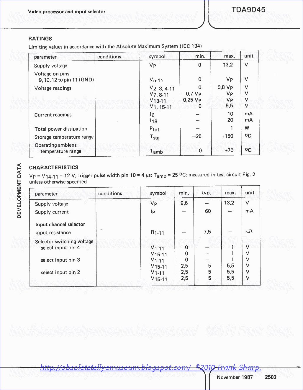


SAA9057 FEATURES
Clock generation suitable for digital TV systems (line» locked)
PLL frequency multiplier to generate 4 times of input frequency
Dividers to generate clocks LL1.5, LL2, LL2A, LL3 and LL3T (41h, 3rd and 2nd multiples 01 input irequency)
Skew control for clock outputs
Reset control and power fail detection
GENERAL DESCRIPTION The SAA9057A generates all clock signals required for a digital TV system suitable for the SAA90xx family.
Optional extras (Feature box etc.) can be driven via external buffers, advantageous for a digital TV system based on display standard conversion concepts.


Features
Pipeline processor structure controls deflection stages
Raster alignment by keyboard or automatically
Adaptable beam current compensation for picture height and width
Protection input stops the exceeding
For double the line frequency and 100-/120-Hz vertical frequency interlaced
Circuit Description
The DDC consists essentially of a processor with pro
gram ROM and RAM, ports for input and output signals and a clock rate divider that supplies the whole chip with clock signals. The processor is specially manufactured for the arithmetic operations performed in the DDC. It operates according to the pipeline principle on account of the high requirements involved with regard to time. It has two 16-bit accumulators. The 16-bit data bus and the 7-bit address bus take care of the data traffic between the processor and the ports. The size of the static RAM is 96 x 16 bits; the program ROM can store 800 16-bit instructions. The V port and the Φ2 port comprise counters for coarse conversion and a chain of 32 resistors for amplitude quantization of fine conversion. The Φ2 port further measures the position of the ZR pulses with respect to time and transfers measured data to the processor. The east/west port similarly has a counter for digital time conversion but manages without fine conversion. The 9-bit analog-to-digital converter works on the principle of successive approximation using a capacitance field. The I2C Bus interface makes it possible to read and modify deflection data in the RAM. The protective circuitry monitors inputs SS, ZR and HA2EN using comparators. The start-up circuitry has its own power and clock pulse supply. It is therefore completely independent of the other DDC functions.Description of the Signal and Data I/O of the Digital Deflection Controller
The digital deflection controller (DDC) generates horizontal-frequency, pulse width modulated control signals for external deflection output stages of color TV sets. The output signal for the horizontal deflection is phase-shifted, the signal for the east/west raster correction is parabolic and the signal for the vertical deflection is saw-tooth modulated. Signal computation is performed with data values from an internal memory that can be written by the I2C Bus. DDC is synchronized by means of a horizontal and a vertical input signal. The HA2 output generates the control signals for a conventional horizontal output stage. The east/west output drives the diode modulator via a switched small-signal transistor. After the integration of the output signal a linear amplifier can be connected to the output VA1 to drive the V-output stage. The above-mentioned data values which determine the raster are stored (system-specific for 45 AX picture tubes) in an integrated ROM for 50-Hz and 60-Hz vertical deflection frequencies. However, individual alignment is possible as well. The data obtained is written into a nonvolatile memory of the operating processor. During switch-on, the data is transferred via the I2C Bus to the deflection RAM in the DDC. In addition, the variable storage time of the horizontal deflection stage transistor is compensated (Φ2 control loop), while the pulse duty factor of the driver-control signal remains constant. The horizontal deflection stage is switched off via a protective circuitry, when the voltage at input SS exceeds a given level. The start-up circuitry supplies the horizontal deflection stage transistor with control signals in the standby mode, the switch-off phase, and during system clock failure. The system includes a control loop with an analog-to-digital converter to stabilize the shape and amplitude of the vertical deflection current (V-feedback). The input signals HS2 and VS2 are supplied with double the frequency from a TV-standard conversion circuitry. The resolution enhancement filter of the VDA can be set via two outputs with the I2C Bus interface of the deflection controller. The DDC can be externally reset via a RESET input (with L level). Deflection frequencies: 100/120-Hz field frequency, 31.25/31.5-kHz line frequency.
Description of the Start-Up Circuitry
The horizontal start-up circuitry is provided with the supply voltage of the operating processor via pin VDD S. This supply voltage is already present in the standby mode of the TV set, although the supply voltage for the horizontal driver and horizontal output stages is not yet available. During standby mode, the HA2 output signal shape corresponds to the standard mode, however, without Φ2 function. The H-level duration is 14.5 μs and the period ranges between 31.6 and 32.55 μs, depending on the tolerance of the ceramic resonator (± 1 %). After the main supply voltage VDD has been switched on and the HA2 signals of the start-up circuitry have been correlated with the HA2 signals arriving from the DDC (Φ2 circuitry), the standard mode is selected within one frame period (max. shift is – 2.8 to + 2.55 μs including all tolerances), if the following requirements are met: – The DDC supplies the start-up circuitry with HA2 signals satisfactory with respect to the period and H-level duration – The ZR-pulse threshold is not exceeded at pin SS – The supply voltage at the horizontal driver exceeds the minimal value (threshold at pin HA2EN, if connected). The standby mode is selected immediately in response to a drop in the DDC-main supply voltage and concomitant max. phase shifts of – 2.65 to + 2.8 μs. The maximum period duration of HA2 with reference to LH junctions may be 36 μs in the event of faults (e.g. failure of LL1.5, malfunctions in the DDC with the exception of the start-up circuitry. The switch-off time constant of VDD S should be larger than that of VDD, ensuring that the HA2 pulses are continuously supplied during a voltage glitch of VDD and exceed the duration of the horizontal output stage voltage supply during switch-off. During all operating modes, HA2 will be high for the duration of the ZR pulse. I2C Bus Protocol The DDC includes a I 2C Bus port designed for the following functions: – Slave receiver – Slave transmitter Since the DDC does not include a master function, data transfers are always initiated and controlled by an external bus master. The actual data transfer is executed by the processor of the DDC serving its I2C Bus port every 32 μs and receiving or transferring data in accordance with the operating mode set. A maximum of 127 memory locations is available for read/write operations via the processor of the DDC.


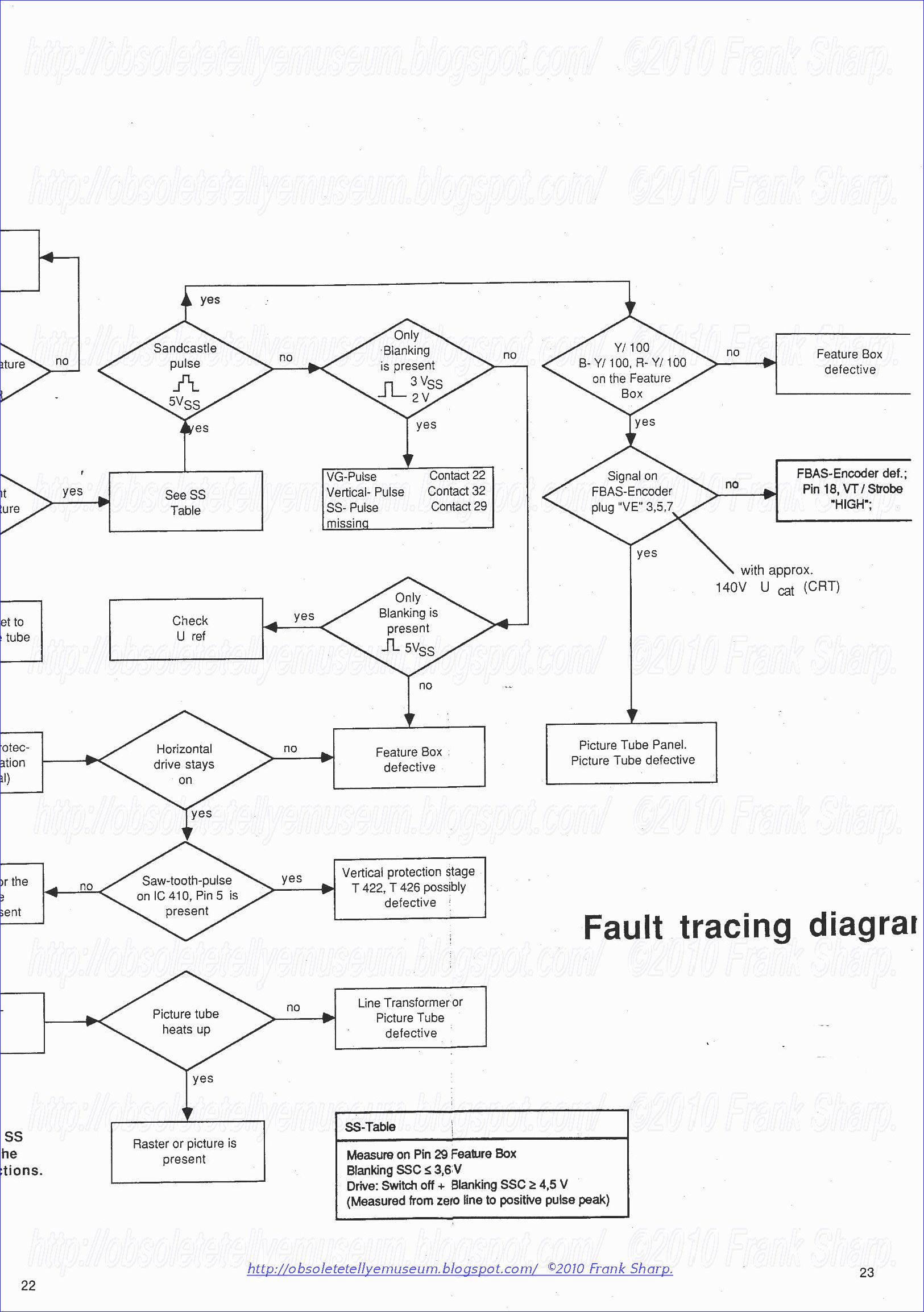


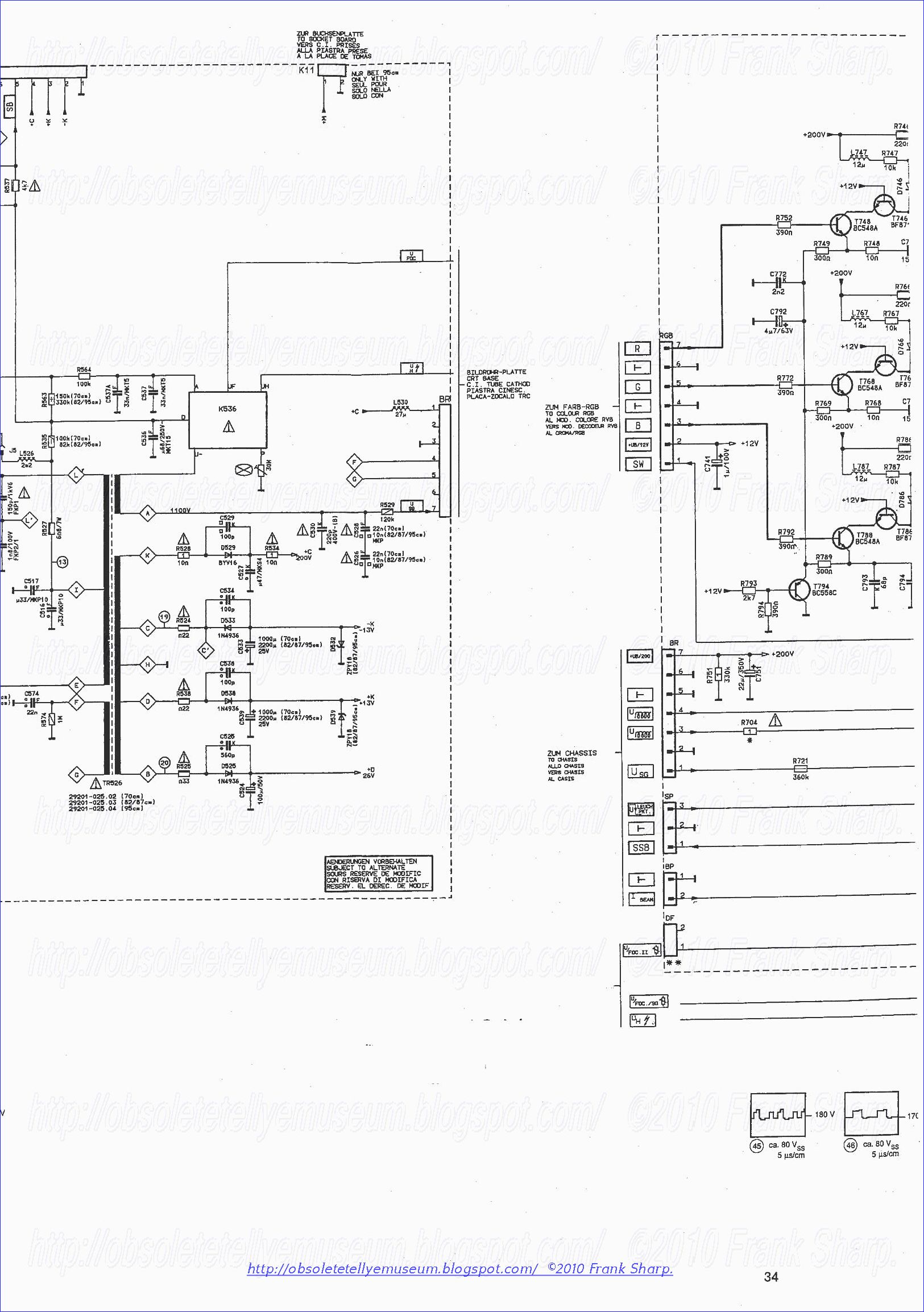


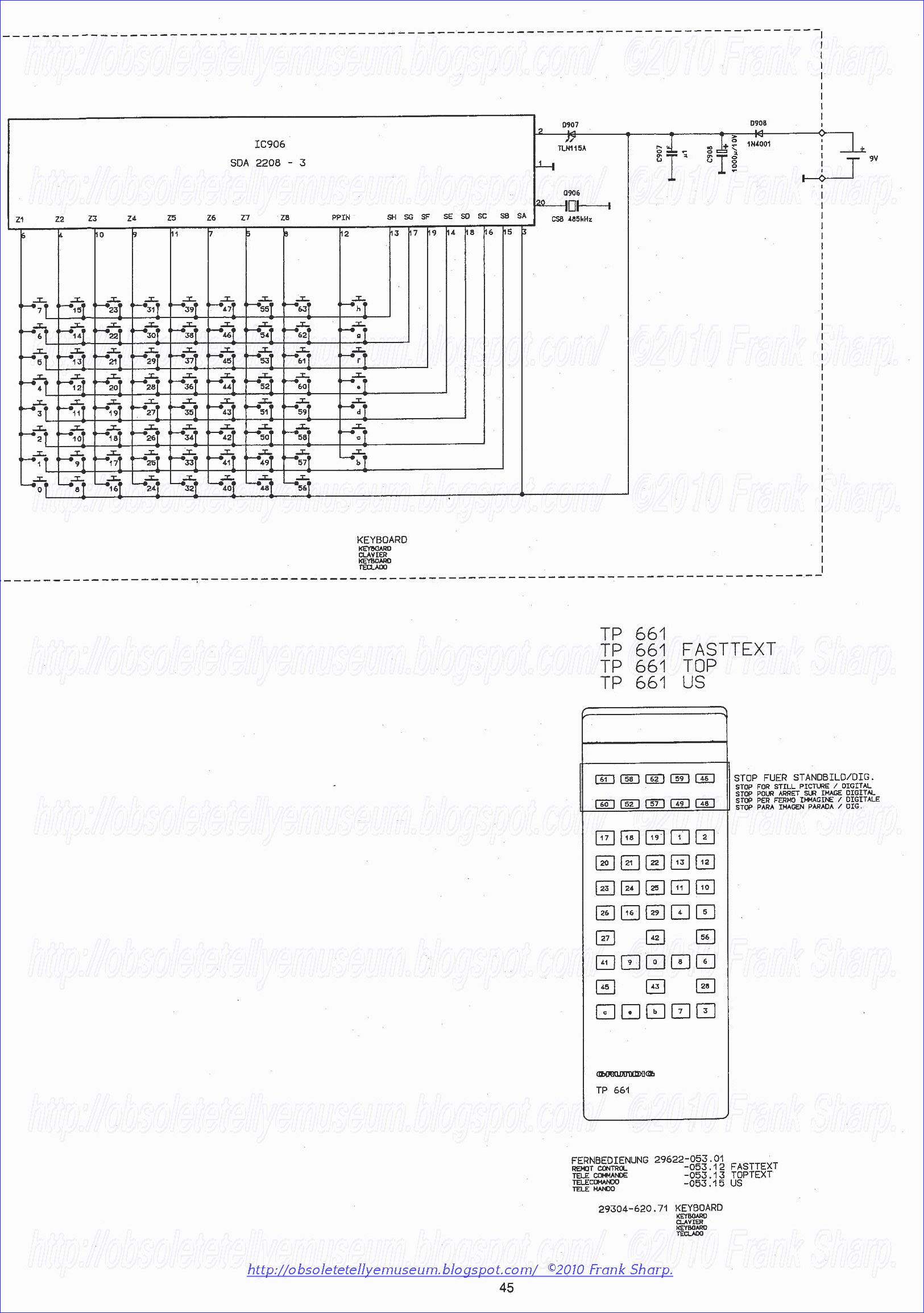


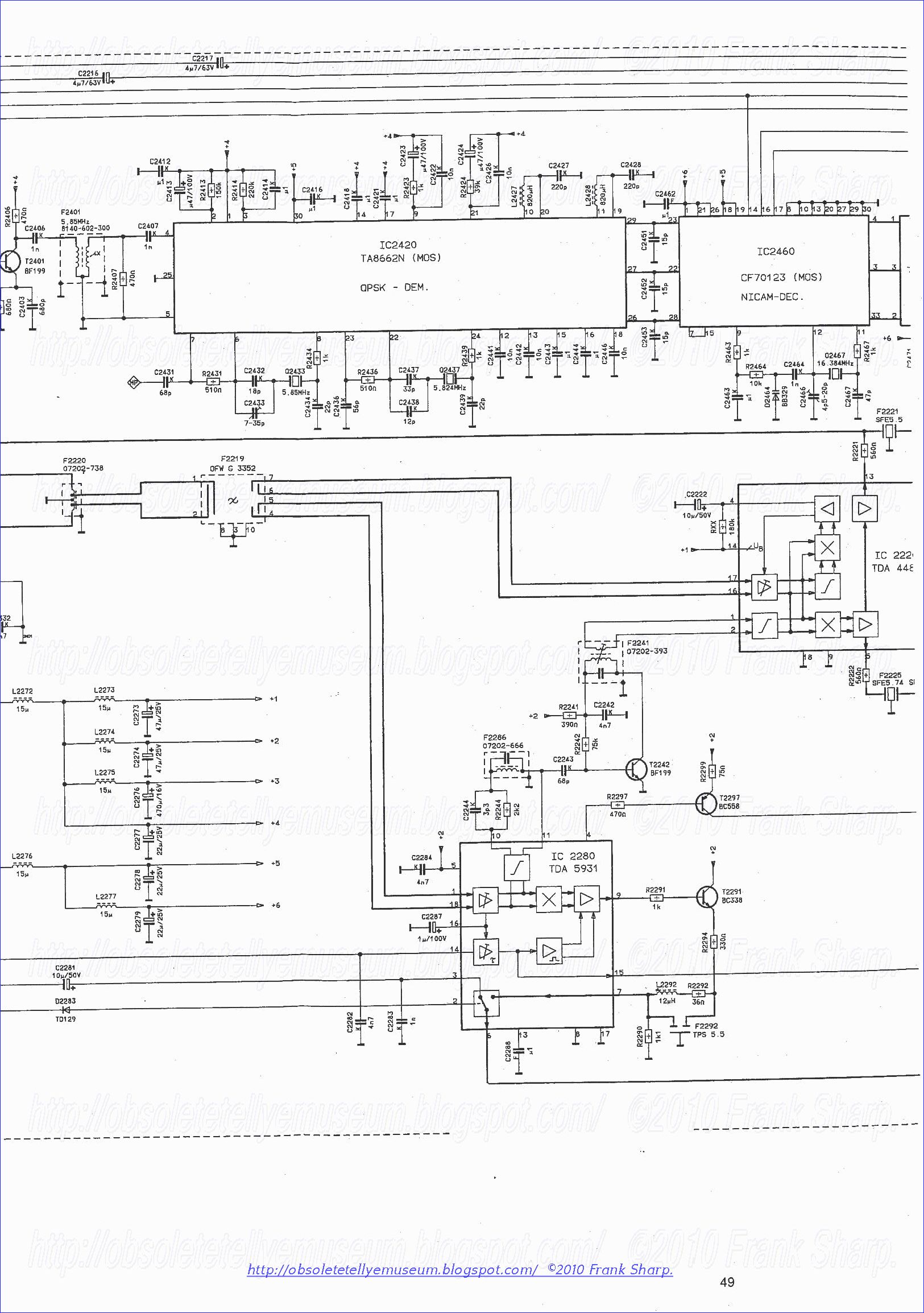

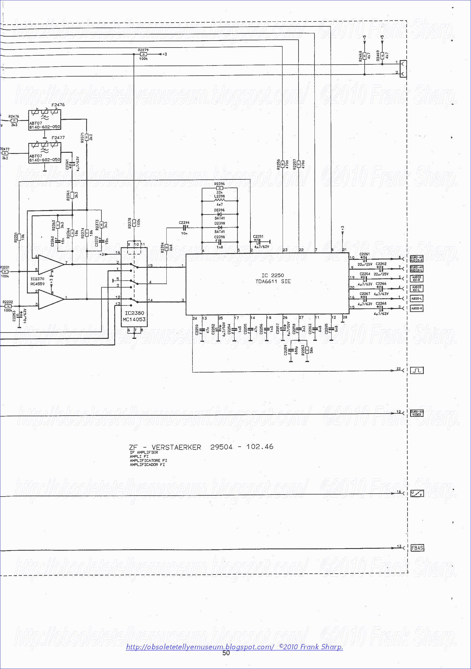


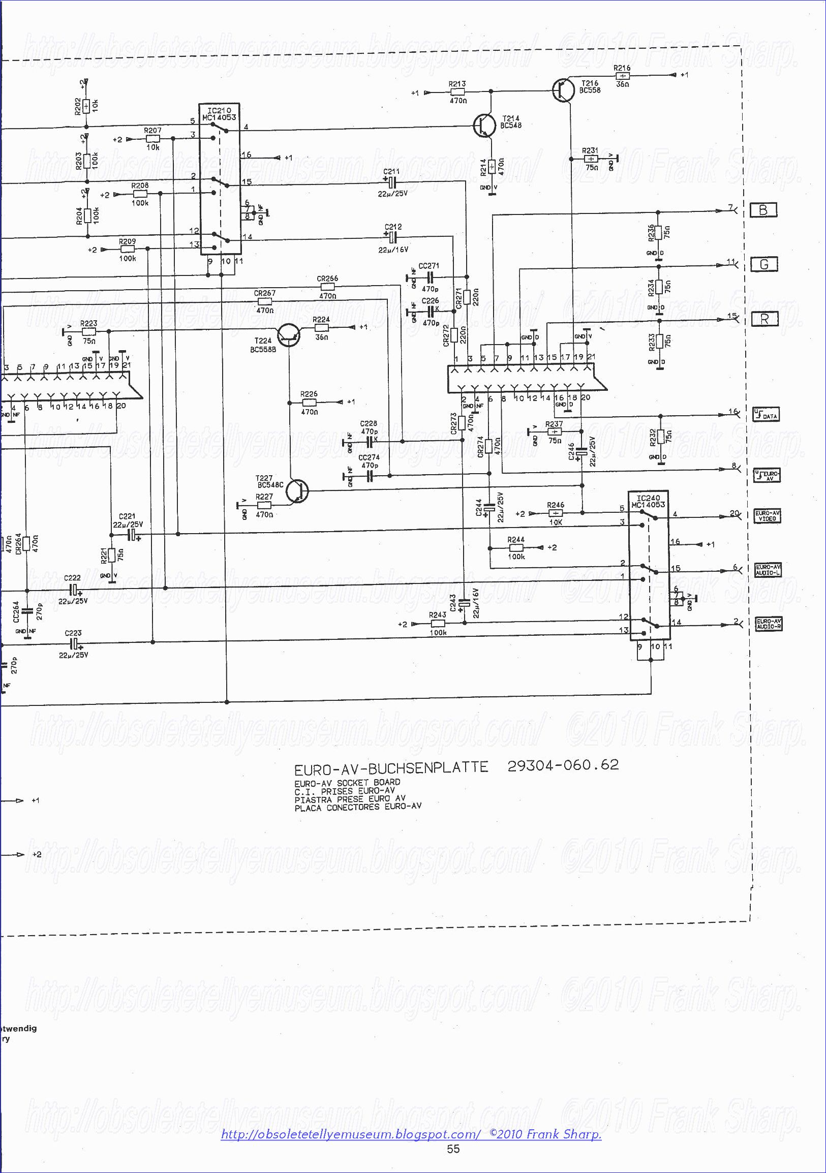


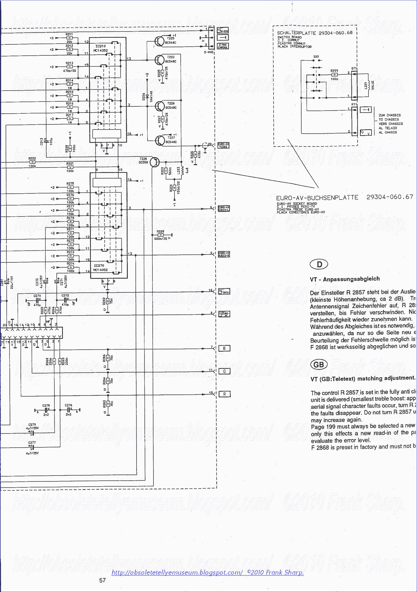


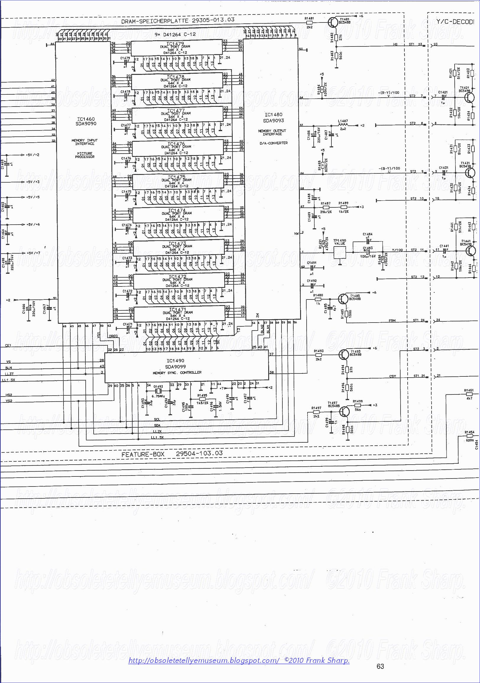


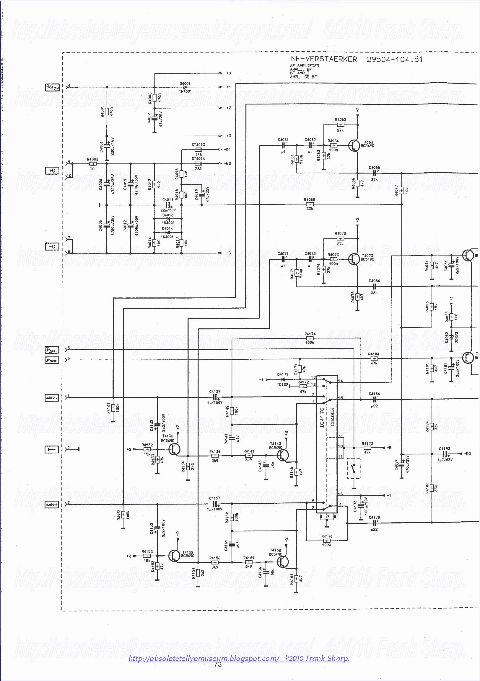


ARTICLE REFERENCES LIST:
A. Semiconductor Devices and Physics
1. J. Baliga and D. Y. Chen (Eds.), Power Transistors: Device Design and Applications, IEEE
Press, New York, 1984.
2. J. Biliga, Modern Power Devices, John Wiley, New York, 1987.
3. Blicher, Thyristor Physics, Springer-Verlag New York Inc.,1976.
4. K. Ghandhi, Semiconductor Power Devices Physics of Operation and Fabrication Technology,
John Wiley & Sons, Inc.,New York, 1977.
5. G. Hoft, Semiconductor Power Electronics, Van Nostrand Reinhold Company Inc.,1986.
(ISBN: 0-442-22543-1)
6. P .
L. Hower, Power semiconductor devices: an overview, IEEE Proc., Wvol. 76, no. 4, pp.
335-342, April 1988.
7. C. Lee and D. Y. Chen (Ed.), Power Devices and Their Applications, Virginia Power
Electronics Center, 1990.
8. Ohmi, Power static induction transistor technology," Technical Digest, IEEE Electron Devices
International Meeting, Washington, D.C., pp. 84-87, 1979.
9. Shockley, A unipolar field-effect transistor ,"
Proc. IRE, vol. 40, pp. 1365-1376, Nov. 1952.
10. Shockley, How we invented the transistor," New Scientist, vol. 689, Dec. 21, 1972.
11. Shockley, The path to the conception of the junction transistor," IEEE Trans. Electron Devices
23, vol. 597, 1976.
12. G. Streetman, Solid State Electronic Devices, Prentice-Hall, Inc., 1980.
13. M. SZE, Semiconductor Devices: Physics and Technology, Bell Telephone Lab., Inc., 1985.
14. Teszner and R. Giqual, Gridistor - a new field-effect device," Proc. IEEE, vol. 52, pp. 1502-
1513, 1964.
15. M. Warner and B. L. Grung, Transistors: Fundamentals for the Integrated-Circuit Engineer
,
1983.
16. Wood, Fundamentals and Applications of Gate Turn-off Thyristors, Electric Power Research
Institute, Palo Alto, 1988.
17. S. Yang, Fundamental of Semiconductor Devices, McGraw-Hill Book Company, 1978.
18. Zuleeg, Multi-Channel field-effect transistor, theory and experiment," Solid-State Electronics,
vol. 10, pp. 559-576, 1967.
B. Power Electronics
19. D. Bedford and R. G. Hoft, Principles of Inverter Circuits, 1985 Reprint Edition, Robert E.
Krieger Publishing Company, Malabar, Florida, 1964.
20. M. Bird and K. G. King, An Introduction to Power Electronics,1983. (ISBN: 0-471-10430-
2)
21. B. K. Bose, Adjustable Speed A C Drive Systems, IEEE Press, New York, 1982.
22. B. K. Bose, "Power electronics - an emerging technology", IEEE Trans. on Ind. Electron., vol.
36, no. 3, pp. 404-412, Aug. 1989.
23. B. K. Bose, Microcomputer Control of Power Electronics and Drives, IEEE Press, New
York, 1987.
24. B. K. Bose., Modern Power Electronics, Evolution, Technology and Applications, IEEE
Press, New York, 1991.
25. B. K. Bose,"Power electronics - an emerging technology," IEEE Trans. on Ind. Electron., vol.
36, no. 3, pp. 403-412, 1989.
26. B. K. Bose, Power Electronics and A C Drives, Prentice Hall, Englewood Cliffs, 1986.
27. B. K. Bose, Power Electronics and A C Drives, Prentice-Hall, New Jersey, 1987.
(TK7881.15.B67).
28. B. K. Bose, "Power electronics and motion control technology," IEEE, pp. 1-10, 1992.
29. B. K. Bose, "Technology trends in microcomputer control of electrical machines," IEEE
Trans. on Ind. Electron., vol. 35, no. 1, pp. 160-177, Feb. 1988.
30. A. Coekin, High-Speed Pulse Techniques, Pergamon, 1975. (TK7835.C56 1975).
31. Csaki, I. Hermann, I. Ipsits, A. Karpati, and P .
Magyar, Power Electronics Akademiai Kiado,
Budapest, 1979. (ISBN 963-05-1671-3).
32. B. Dewan and A. Straughen, Power Semiconductor Circuits, John Wiley & Sons, Inc., 1975.
33. K. Dubey, Power Semiconductor Controlled Drives, Prentice Hall, Englewood Cliffs, 1985.
34. Hans-Peter Hempel, Power Semiconductor Handbook, SEMIKRON, 1980. (ISBN 3-
9800346-1-5).
35. R. G. Hoft, Semiconductor Power Electronics, Van Nostrand, New York, 1986.
(TK7871.85.H65).
36. L. Kusic, Computer-Aided Power Systems Analysis, Prentice-Hall, 1986. (TK1005.K87
1986).
37. W. Lander ,
Power Electronics, McGraw-Hill, 1981. (ISBN: 0-07-084123-3).
38. M. Miller, Is power electronics a national priority ?, Power Conversion & Intelligent
Motion Control, March 1987.
39. Mohan, T. M. Undeeland, and P .
Robbins, Power Electronics, John Wiley, New York, 1989.
40. M. D. Murphy and F. G. Turnbull, Power Electronic Control of A C Motors, Pergamon, New
York, 1988.
41. E. Newell and J. W. Motto, Introduction to Solid State Power Electronics, Youngwood:
Westinghouse Electric Corporation, 1977.
42. S. Oxner, Power FETs and Their Applications, Prentice-Hall Inc., 1982.
43. Pearman, Power Electronics: Solid State Motor Control, Reston Publishing Company, Inc.,
1980.
44. Pearman, Solid State Industrial Electronics, Reston Publishing Company, Inc., 1984. (ISBN:
0-8359-7041-8) (TK7881.P43).
45. Rajagopalan, Computer Aided Analysis of Power Electronic Systems, Marcel Dekker, New
York, 1987.
46. H. Rashid, Power Electronics, Prentice Hall, Englewood Cliffs, 1988.
47. H. Seidman, H. Mahrous, and T. G. Hicks, Handbook of Electric Power Calculations, 1983.
(ISBN 0-07-056061-7).
48. P .
Severns and G. E. Bloom, Modern DC-to-DC Switchmode Power Converter Circuits,
Van Nostrand Reihold Company Inc..
49. E. Tarter ,
Principles of Solid State Power Conversion, Howard W. Sams, 1985.
50. W. Williams, Power Electronics, John Wiley, New York, 1987.
C. Power Supplies
D. Electronic51. Chryssis, High-Frequency Switching Power Supplies Theory and Design, McGraw-Hill,
1984. (ISBN 0-07-010949-4) (TK868.P6C47).
52. Gottlieb, Regulated Power Supplies, third edition, Howard W. Sams & Co., Inc., 1984.
53. Gottlieb, Power Supplies: Switching Regulators Inverters & Converters, 1984.
54. Griffith, Uninterruptible Power Supplies, Marcel Dekker, New York, 1989.
55. Hnatek, Design of Solid State Power Supplies, Van Nostrand, New York, 1981.
56. Lee (Ed.), High-Frequency Resonant, Quasi-Resonant, and Multi-Resonant Converters,
Virginia Power Electronics Center, 1989.
57. Lee (Ed.), Modeling, Analysis, and Design of PW M Converters, Virginia Power
Electronics Center, 1990.
58. Middlebrook and S. Cuk (Eds.), Advances in Switching Mode Power Conversion, vols. I &
II, TESL A Co., Pasadena, California 1983.
59. M OTOROL A, Switchmode Application Manual, Motorola Inc., 1981.
60. M OTOROL A, Linear/Switchingmode Voltage Regulator Handbook: Theory and
Practice, 1981.
61. Pressman, Switching and Linear Power Supply, Power Converter Design, Hayden,
Rochelle Park, 1977.
62. Rensink, Switching Regulator Configurations and Circuit Realization, Ph.D Thesis by
Loman Rensink, California, 1979.
63. Severns and G. E. Bloom, Modern DC - to - DC Switch Mode Power Converter Circuits,
Van Nostrand, New York, 1985.
64. Sum, Switch Mode Power Conversion: Basic Theory and Design, Marcel Dekker, New
York, 1984.
65. Wood, Switching Power Converters, Van Nostrand, New York, 1981.
66. UNITRODE, Unitrode Switching Regulated Power Supply Design Seminar Manual,
Unitrode Corporation, 1985.
67. UNITRODE, Applications Handbook, Unitrode Corporation, 1985.
Equipment Thermal Design, Package Design
68. N. Ellison, Thermal Computations for Electronic Equipment, Van Nostrand Reinhold
Company, New York, 1984.
69. D. Kraus and Avram Bar-Cohen, Thermal Analysis and Control of Electronic Equipment,
Hemisphere Publishing Corporation, Washington, 1983. (ISBN 0-07-035416-2)
(TK7870.25.K73).
70. S. Matisoff, Handbook of Electronics Packaging Design and Engineering, Van Nostrand
Reinhold Company, 1982.
71. S. Steinberg, Cooling Techniques for Electronic Equipment, John Wiely & Sons, Inc., 1980.
(TK7870.25.S73).
E. Noise Reduction Techniques
72. W. Denny, Grounding for the Control of E MI.
73. J. Geogopoulos, Fiber Optics and Optical Isolators.
74. N. Ghose, E MP Environment and System Hardness Design.
75. C. Hart and E. W. Malone, Lighting and Lighting Protection.
76. Mardiguian, Electrostatic Discharge - Understand, Simulate and Fix ESD Problems.
77. Mardiguian, Interference Control in Computers and Microprocessor-Based Equipment.
78. Mardiguian, How to Control Electrical Noise.
79. Morrison, Grounding and Shielding Techniques in Instrumentation, second edition, John
Wiley & Sons, Inc., 1977.
80. Morrison, Instrumentation Fundamentals and Applications, John Wiley & Sons, Inc., 1984.
81. W. Ott, Noise Reduction Techniques in Electronic Systems, Wiley-Interscience Publication,
1976.
82. A. Smith, Coupling of External Electromagnetic Fields to Transmission Lines.
83. R. J. White and M. Mardiguian, E MI Control Methodolgy and Procedures.
84. R. J. White, E MI Control in the Design of Printed Circuit Boards and Backplanes, 248 Pages.
85. R. J. White, Shielding Design Methodlogy and Procedures.
86. R. J. White, Electrical Filter
.
87. R. J. White, Electromagnetic Shielding Materials and Performance.
88. E MC E XPO, 1986 Symposium Record, 416 Pages.
89. E MC Library :
vol. 1 Electrical Noise and E MI Specifications
vol. 2 E MI Test Methods and Procedures
vol. 3 E MI Control Methods and Techniques
vol. 4 E MI Test Instrumentation and Systems
vol. 5 E MI Prediction and Analysis Techniques
vol. 6 E MI Specifications, Standards, and Regulations
More References:
[1] Paynter, D.A., AN UNSYMMETRICAL SQUARE-WAVE
POWER OSCILLATOR, IRE transactions on Circuit Theory,
March 1956, pp. 64-65
[2] Dudley, William, UNSYMMETRICAL LOW VOLTAGE CON-
VERTER, 17th Power Sources Conference proceedings, 1963, pp.
155-158
[3] van Velthooven, C., PROPERTIES OF DC-TO-DC CONVERT-
ERS FOR SWITCHED-MODE POWER SUPPLIES, Philips
Application Information #472, 18 March 1975, pp. 8-10
[4] G. Wolf, MAINS ISOLATING SWITCH-MODE POWER SUP-
PLY, Philips Electronic Applications Bulleting, Vol. 32, No. 1,
February 1973
[5] La Duca and Massey, IMPROVED SINGLE-ENDED REGU-
LATED DC/DC CONVERTER CIRCUIT, IEEE Power Electronics
Specialists Conference (PESC) record, June 1975, pp. 177-187
[6] Heinicke, Harald, APPARATUS FOR CONVERTING D.C.
VOLTAGE, U.S. patent number 3,921,054, 18 November 1975
(1973 German filing)
[7] Hamata and Katou, DC-TO-DC CONVERTER, U.S. patent
number 3,935,526, 27 January 1976 (1972 Japanese filing)
[8] Peterson, W.A., A FREQUENCY-STABILIZED FREE-RUN-
NING DC-TO-DC CONVERTER CIRCUIT EMPLOYING
PULSE-WIDTH CONTROL REGULATION, IEEE PESC proceed-
ings, June 1976, pp. 200-205
[9] Vermolen, J.V., NON-SATURATING ASYMMETRIC DC/DC
CONVERTER, U.S. patent number 3,963,973, 15 June 1976 (1973
Dutch filing)
[10] Lilienstein and Miller, THE BIASED TRANSFORMER DC-
TO-DC CONVERTER, IEEE PESC proceedings, June 1976, pp.
190-199
[11] Carsten, B., HIGH POWER SMPS REQUIRE INTRINSIC
RELIABILITY, Power Conversion International (PCI) proceedings,
September 1981, pp. 118-133
[12] Kuwabara and Miyachika, A VERY WIDE INPUT RANGE
DC-DC CONVERTER, IEEE INTELEC proceedings, 1987, pp.
228-233
[13] Wittenbreder, Martin and Baggerly, A DUTY CYCLE
EXTENSION TECHNIQUE FOR SINGLE ENDED FORWARD
CONVERTERS, IEEE Applied Power Electronics Conference
(APEC) proceedings, 1992, pp. 51-57
More References:
Buhler H (1986) Sliding mode control (in French: Reglage ́
par mode de glissement). Presses
Polytechniques Romandes, Lausanne
Carpita M, Marchesoni M (1996) Experimental study of a power conditioning system using sliding
mode control. IEEE Trans Power Electron 11(5):731–742
Carrasco JM, Quero JM, Ridao FP, Perales MA, Franquelo LG (1997) Sliding mode control of a
DC/DC PWM converter with PFC implemented by neural networks. IEEE Trans Circuit Syst I
Fundam Theor Appl 44(8):743–749
DeBattista H, Mantz RJ, Christiansen CF (2000) Dynamical sliding mode power control of wind
driven induction generators. IEEE Trans Energy Convers 15(4):728–734
DeCarlo RA, Zak ̇
SH, Drakunov SV (2011) Variable structure, sliding mode controller design. In:
Levine WS (ed) The control handbook—control system advanced methods. CRC Press, Taylor
& Francis Group, Boca Raton, pp 50-1–50-22Radar, optical communication, tuners and RF modules, RF
ICs, communication systems, audio and analogue, IC technology and
packaging, semiconductor and module packaging for non-RF an RF-
applications, by Pieter Hooijmans, www.maximus-randd.com.
Emelyanov SV (1967) Variable structure control systems. Nauka, Moscow (in Russian)
Filippov AF (1960) Differential equations with discontinuous right hand side. Am Math Soc
Transl 62:199–231
Guffon S (2000) Modelling and variable structure control for active power filters (in French:
“Modelisation ́
et commandes `
a structure variable de filtres actifs de puissance”). Ph.D. thesis,
Grenoble Institute of Technology, France
Guffon S, Toledo AS, Bacha S, Bornard G (1998) Indirect sliding mode control of a three-phase
active power filter. In: Proceedings of the 29th annual IEEE Power Electronics Specialists
Conference – PESC 1998. Kyushu Island, Japan, pp 1408–1414
Hung JY, Gao W, Hung JC (1993) Variable structure control: a survey. IEEE Trans Ind Electron
40(1):2–22
Itkis U (1976) Control systems of variable structure. Wiley, New York
Levant A (2007) Principles of 2-sliding mode design. Automatica 43(4):576–586
Levant A (2010) Chattering analysis. IEEE Trans Autom Control 55(6):1380–1389
Malesani L, Rossetto L, Spiazzi G, Tenti P (1995) Performance optimization of Cuk ́
converters by
sliding-mode control. IEEE Trans Power Electron 10(3):302–309
Malesani L, Rossetto L, Spiazzi G, Zuccato A (1996) An AC power supply with sliding mode
control. IEEE Ind Appl Mag 2(5):32–38
Martinez-Salamero L, Calvente J, Giral R, Poveda A, Fossas E (1998) Analysis of a bidirectional
coupled-inductor Cuk ́
converter operating in sliding mode. IEEE Trans Circuit Syst I Fundam
Theor Appl 45(4):355–363
Mattavelli P, Rossetto L, Spiazzi G (1997) Small-signal analysis of DC–DC converters with
sliding mode control. IEEE Trans Power Electron 12(1):96–102
ˇ
Sabanovic A (2011) Variable structure systems with sliding modes in motion control—a survey.
IEEE Trans Ind Inform 7(2):212–223
Sabanovic ˇ
A, Fridman L, Spurgeon S (2004) Variable structure systems: from principles to
implementation, IEE Control Engineering Series. The Institution of Engineering and Technol-
ogy, London
Sira-Ramırez ́ H (1987) Sliding motions in bilinear switched networks. IEEE Trans Circuit Syst 34
(8):919–933
Sira-Ramırez ́
H (1988) Sliding mode control on slow manifolds of DC to DC power converters. Int
J Control 47(5):1323–1340
Sira-Ramırez ́
H (1993) On the dynamical sliding mode control of nonlinear systems. Int J Control
57(5):1039–1061
Sira-Ramırez ́
H (2003) On the generalized PI sliding mode control of DC-to-DC power converters:
a tutorial. Int J Control 76(9/10):1018–1033
Sira-Ramırez ́
H, Silva-Ortigoza R (2006) Control design techniques in power electronics devices.
Springer, London
Slotine JJE, Sastry SS (1983) Tracking control of non-linear systems using sliding surface, with
application to robot manipulators. Int J Control 38(2):465–492
Spiazzi G, Mattavelli P, Rossetto L, Malesani L (1995) Application of sliding mode control to
switch-mode power supplies. J Circuit Syst Comput 5(3):337–354
Tan S-C, Lai YM, Cheung KHM, Tse C-K (2005) On the practical design of a sliding mode
voltage controlled buck converter. IEEE Trans Power Electron 20(2):425–437
Tan S-C, Lai Y-M, Tse C-K (2011) Sliding mode control of switching power converters:
techniques and implementation. CRC Press, Taylor & Francis Group, Boca Raton
Utkin VA (1972) Equations of sliding mode in discontinuous systems. Autom Remote Control 2
(2):211–219
Utkin VA (1977) Variable structure systems with sliding mode. IEEE Trans Autom Control 22
(2):212–222
Utkin V (1993) Sliding mode control design principles and applications to electric drives. IEEE
Trans Ind Electron 40(1):23–36
Venkataramanan R, Sabanovic ˇ
A, Cuk ́
S (1985) Sliding mode control of DC-to-DC converters. In:
Proceedings of IEEE Industrial Electronics Conference – IECON 1985. San Francisco,
California, USA, pp 251–258
Young KD, Utkin VI, Ozguner U (1999) A control engineer’s guide to sliding mode control. IEEE
Trans Control Syst Technol 7(3):328–342
References
[1] Nave, M. J.; “The Effect of Duty Cycle on SMPS Common Mode Emissions: Theory
and Experiment”, IEEE 1989 National Symposium on 23-25 May, 1989
[2] Cochrane, D.; Chen, D. Y.; Boroyevic, D.; “Passive Cancellation of Common-Mode
Noise in Power Electronic Circuits”, IEEE Transactions on Power Electronics,
Volume 18, Issue 3, May 2003
[3] Qu, S.; Chen, D. Y.; “Mixed-Mode EMI Noise and Its Implications to Filter Design in
Offline Switching Power Supplies”, Applied Power Electronics Conference and
Exposition, 2000, Fifteenth Annual IEEE, Volume 2, 6-10 Feb. 2000
[4] “Mounting Considerations For Power Semiconductors”, On Semiconductor Application
Note AN1040/D, May 2001-Rev. 3
[5] Mardiguian, M.; “Controlling Radiated Emissions by Design”, Chapman & Hall,
ISBN 0442009496
[6] Mardiguian, M.; “How To Control Electrical Noise”, 2nd Edition, 1983, Don White
Consultants, Inc., State Route #625, P.O. Box D, Gainesville, Virginia 22065, USA
[7] Hayt, H. W. JR.; “Engineering Electromagnetics”, Fourth Edition, McGraw-Hill Book
Company, ISBN 0070273952
[8] Collett, P. C. E.; “Investigations into Aspects Affecting the Design of Mains Filters for
Frequencies in the Range 10kHz-30MHz”, ERA Report No. 82-145R, 1983, ERA
Technology Ltd., Cleeve Road, Leatherhead, Surrey KT22 7SA, England
[9] “Capacitors for RFI Suppression of the AC Line: Basic Facts”, Fourth Edition,
Evox-Rifa Application Notes, Evox-Rifa Inc., 300 Tri-State International, Su. 375,
Lincolnshire, IL 60069, USA
[10] “Conducted Emission Performance of Ericsson DC/DC power modules:
Characterization and System Design”, Ericsson Design Note 009, April 2000, Ericsson
Microelectronics AB
[11] Ott, H. W.; “Noise Reduction Techniques in Electronic Systems”, Second Edition,
1987, John Wiley & Sons, ISBN 0471850683
[12] Ott, H. W.; “Understanding and Controlling Common-Mode Emissions in High-Power
Electronics”, Applied Power Electronics Conference and Exposition, 2002
[13] Basso, C.; “Conducted EMI Filter Design for the NCP1200”, On Semiconductor
Application Note AND8032/D
More listed References
[14] Armstrong, K.; Williams, T.; “EMC Testing”, Parts 1 through 6; Cherry Clough
Consultants and Elmac Services, UK
[15] Bergh, K.; “CISPR 22 Telecom Ports”, NEMKO Seminar, 2001
[16] “EMC of Monitors”, Philips Semiconductors Application Note AN 00038
[17] “EMI Testing Fundamentals”, Steward Technical Information
[18] Savino, S. E.; Suranyi, G. G.; “Application Guidelines for On-Board Power
Converters”, Tyco Electronics Application Note, June 1997
[19] “Input System Instability”, Synqor Application Note PQ-00-05-01 Rev.01-5/16/00
[20] Collett, P. C. E.; “Investigations into Aspects Affecting the Design of Mains Filters
for Frequencies in the Range 10kHz-30MHz”, ERA Report No. 82-145R, 1983,
ERA Technology Ltd., Cleeve Road, Leatherhead, Surrey KT22 7SA,
England
[21] “Capacitors for RFI Suppression of the AC Line: Basic Facts”, Fourth Edition,
Evox-Rifa Application Notes, Evox-Rifa Inc., 300 Tri-State International, Su. 375,
Lincolnshire, IL 60069, USA
[22] Snelling, E. C.; “Soft Ferrites, Properties and Applications”, Second Edition, ISBN
0408027606; Butterworths & Co.
[23] “Power Factor Corrector, Application Manual”, 1st Edition, October 1995;
SGS-Thomson Microelectronics
[24] “Data Handbook, Aluminum Electrolytic Capacitors”, PA01-A, 1993 N.A. Edition;
Philips Components
[25] “Understanding Aluminum Electrolytic Capacitors”, nd Edition, 1995; United
2Chemi-Con Inc.
[26] Micro Linear Corporation Data Book, 1995
[27] “Fair-Rite Soft Ferrites”, Databook, 13th Edition; Fair-Rite Products Corp. NY 12589
[28] “Magnetics Designer”, Supplementary Information, 1997; Intusoft
[29] “UC3842/3/4/5 Provides Low-cost Current-mode Control”, Application Note, U-100A;
Unitrode Integrated Circuits
[30] Billings, K. H.; “Switchmode Power Supply Handbook”, 1989, ISBN 0070053308;
McGraw-Hill Inc.
[31] Pressman, A. I.; “Switching Power Supply Design”, 1991, ISBN 0070508062,
McGraw Hill Inc.
[32] McLyman, W. T.; “Transformer and Inductor Design Handbook”, nd Edition, 1988,
2ISBN 0824778286; Marcel Dekker, Inc.
[33] Unitrode Power Supply Design Seminar, SEM-500, Unitrode Integrated Circuits
[34] “3C85 Handbook”, 1987, Ordering Code 9398 345 90011; Philips Electronic
Components and Materials
[35] Sum, K. K.; “Intuitive Magnetic Design”, Nov 15-16, 2000, Electronic Design
Workshops; Penton Media, Inc.
Others References list
[36] Bloom, G. E.; “DC-DC Switchmode Power Converters, Circuits and Converters”,
April 25, 2002, National Semiconductor Corporation Seminar Presentation; Bloom
Associates Inc., CA-94903
[37] Mulder, S. A.; “Application Note on the design of low profile high frequency
transformers, a new tool in SMPS design”, 1990, Ordering Code 9398 074 80011;
Philips Components Corporate Innovation Materials
[38] Ahmadi, H.; “Calculating Creepage and Clearance Early Avoids Design Problems
Later”, March/April 2001; Compliance Engineering Magazine
[39] Redl, R.; “Low-Cost Line-Harmonics Reduction”, 1995 Seminar in Bremen, Germany;
Power Quality Conference
[40] Carsten, B.; “Calculating Skin and Proximity Effect, Conductor Losses in Switchmode
Magnetics”, 1995, PCIM Conference
[41] “Magnetics® Ferrites”, Databook, 1999; Magnetics Inc., Division of Spang and
Company
[42] Lee, S.; “Thermal Management of Electronic Equipment”, 1996, PCIM Conference
[43] Middlebrook, R. D.; Cuk, S.; “Advances in Switched-Mode Power Conversion:
Volumes I, II, and III”, TESLAco, 10 Mauchly, Irvine, CA 92618
[44] Middlebrook, R. D.; “Topics in Multiple-loop Regulators and Current-mode
Programming”, IEEE 1985
[45] Erickson, R. W.; “Fundamentals of Power Electronics”, Springer, Second Edition,
ISBN 0792372700
[46] “Control Design Lecture Notes”, Center for Power Electronics Systems, June 2-6,
2003, Virginia Polytechnic Institute and State University, Blacksburg, Virginia
[47] Maniktala, S.; “Switching Power Supply Design and Optimization”, McGraw-Hill
Professional, First Edition, ISBN 0071434836
Other References
Buhler H (1986) Sliding mode control (in French: Reglage ́
par mode de glissement). Presses
Polytechniques Romandes, Lausanne
Carpita M, Marchesoni M (1996) Experimental study of a power conditioning system using sliding
mode control. IEEE Trans Power Electron 11(5):731–742
Carrasco JM, Quero JM, Ridao FP, Perales MA, Franquelo LG (1997) Sliding mode control of a
DC/DC PWM converter with PFC implemented by neural networks. IEEE Trans Circuit Syst I
Fundam Theor Appl 44(8):743–749
DeBattista H, Mantz RJ, Christiansen CF (2000) Dynamical sliding mode power control of wind
driven induction generators. IEEE Trans Energy Convers 15(4):728–734
DeCarlo RA, Zak ̇
SH, Drakunov SV (2011) Variable structure, sliding mode controller design. In:
Levine WS (ed) The control handbook—control system advanced methods. CRC Press, Taylor
& Francis Group, Boca Raton, pp 50-1–50-22
Emelyanov SV (1967) Variable structure control systems. Nauka, Moscow (in Russian)
Filippov AF (1960) Differential equations with discontinuous right hand side. Am Math Soc
Transl 62:199–231
Guffon S (2000) Modelling and variable structure control for active power filters (in French:
“Modelisation ́
et commandes `
a structure variable de filtres actifs de puissance”). Ph.D. thesis,
Grenoble Institute of Technology, France
Guffon S, Toledo AS, Bacha S, Bornard G (1998) Indirect sliding mode control of a three-phase
active power filter. In: Proceedings of the 29th annual IEEE Power Electronics Specialists
Conference – PESC 1998. Kyushu Island, Japan, pp 1408–1414
Hung JY, Gao W, Hung JC (1993) Variable structure control: a survey. IEEE Trans Ind Electron
40(1):2–22
Itkis U (1976) Control systems of variable structure. Wiley, New York
Levant A (2007) Principles of 2-sliding mode design. Automatica 43(4):576–586
Levant A (2010) Chattering analysis. IEEE Trans Autom Control 55(6):1380–1389
Malesani L, Rossetto L, Spiazzi G, Tenti P (1995) Performance optimization of Cuk ́
converters by
sliding-mode control. IEEE Trans Power Electron 10(3):302–309
Malesani L, Rossetto L, Spiazzi G, Zuccato A (1996) An AC power supply with sliding mode
control. IEEE Ind Appl Mag 2(5):32–38
Martinez-Salamero L, Calvente J, Giral R, Poveda A, Fossas E (1998) Analysis of a bidirectional
coupled-inductor Cuk ́
converter operating in sliding mode. IEEE Trans Circuit Syst I Fundam
Theor Appl 45(4):355–363
Mattavelli P, Rossetto L, Spiazzi G (1997) Small-signal analysis of DC–DC converters with
sliding mode control. IEEE Trans Power Electron 12(1):96–102
ˇ
Sabanovic A (2011) Variable structure systems with sliding modes in motion control—a survey.
IEEE Trans Ind Inform 7(2):212–223
Sabanovic ˇ
A, Fridman L, Spurgeon S (2004) Variable structure systems: from principles to
implementation, IEE Control Engineering Series. The Institution of Engineering and Technol-
ogy, London
References:
Sira-Ramırez ́
H (1987) Sliding motions in bilinear switched networks. IEEE Trans Circuit Syst 34
(8):919–933
Sira-Ramırez ́
H (1988) Sliding mode control on slow manifolds of DC to DC power converters. Int
J Control 47(5):1323–1340
Sira-Ramırez ́
H (1993) On the dynamical sliding mode control of nonlinear systems. Int J Control
57(5):1039–1061
Sira-Ramırez ́
H (2003) On the generalized PI sliding mode control of DC-to-DC power converters:
a tutorial. Int J Control 76(9/10):1018–1033
Sira-Ramırez ́
H, Silva-Ortigoza R (2006) Control design techniques in power electronics devices.
Springer, London
Slotine JJE, Sastry SS (1983) Tracking control of non-linear systems using sliding surface, with
application to robot manipulators. Int J Control 38(2):465–492
Spiazzi G, Mattavelli P, Rossetto L, Malesani L (1995) Application of sliding mode control to
switch-mode power supplies. J Circuit Syst Comput 5(3):337–354
Tan S-C, Lai YM, Cheung KHM, Tse C-K (2005) On the practical design of a sliding mode
voltage controlled buck converter. IEEE Trans Power Electron 20(2):425–437
Tan S-C, Lai Y-M, Tse C-K (2011) Sliding mode control of switching power converters:
techniques and implementation. CRC Press, Taylor & Francis Group, Boca Raton
Utkin VA (1972) Equations of sliding mode in discontinuous systems. Autom Remote Control 2
(2):211–219
Utkin VA (1977) Variable structure systems with sliding mode. IEEE Trans Autom Control 22
(2):212–222
Utkin V (1993) Sliding mode control design principles and applications to electric drives. IEEE
Trans Ind Electron 40(1):23–36
Venkataramanan R, Sabanovic ˇ
A, Cuk ́
S (1985) Sliding mode control of DC-to-DC converters. In:
Proceedings of IEEE Industrial Electronics Conference – IECON 1985. San Francisco,
California, USA, pp 251–258
Young KD, Utkin VI, Ozguner U (1999) A control engineer’s guide to sliding mode control. IEEE
Trans Control Syst Technol 7(3):328–342
REFERENCES
1. McLyman, Colonel Wm. T., Transformer and Inductor Design Handbook, Marcel Dekker, New York,
1978. ISBN 0-8247-6801-9.
2. McLyman, Colonel Wm. T., Magnetic Core Selection for Transformers and Inductors, Marcel Dekker,
New York, 1982. ISBN 0-8247-1873-9.
3. Kraus, John D., Ph.D., Electromagnetics, McGraw-Hill, New York, 1953.
4. Boll, Richard, Soft Magnetic Materials, Heydon & Sons, London, 1979. ISBN 0-85501-263-3. & ISBN
3-8009-1272-4.
5. Smith, Steve, Magnetic Components, Van Nostrand Reinhold, New York, 1985. ISBN 0-442-20397-7.
6. Grossner, Nathan R., Transformers for Electronic Circuits, McGraw-Hill, New York, 1983. ISBN 0-07-
024979-2.
7. Lee, R., Electronic Transformers and Circuits, Wiley, New York, 1955.
8. Snelling, E. C., Soft Ferrites—Properties and Applications, Iliffe, London, 1969.
9. Middlebrook, R. D., and Cuk, ́
Slobodan, Advances in Switch Power Conversion, Vols. I and II, Teslaco,
Calif., 1983.
́
10. Cuk, Slobodan, and Middlebrook, R. D., Advances in Switchmode Power Conversion, Vol. III, Teslaco,
Calif., 1983.
11. Landee, Davis, and Albrecht, Electronic Designer’s Handbook, McGraw-Hill, New York, 1957.
12. The Royal Signals, Handbook of Line Communications, Her Majesty’s Stationery Office, 1947.
13. Langford-Smith, F., Radio Designer’s Handbook, Iliffe & Son, London, 1953.
14. Pressman, Abraham I., Switching and Linear Power Supply, Power Converter Design, Haydon, 1977.
ISBN 0-8104-5847-0.
15. Dixon, Lloyd H., and Potel Raoji, Unitrode Switching Regulated Power Supply Design Seminar Manual,
1985.
16. Severns, Rudolph P., and Bloom, Gordon E., Modern DC-to-DC Switchmode Power Converter Circuits,
Van Nostrand Reinhold, New York, 1985. ISBN 0-422-21396-4.
17. Hnatek, Eugene R., Design of Solid-State Power Supplies, 2d Ed., Van Nostrand Reinhold, New York,
1981. ISBN 0-442-23429-5.
18. Shepard, Jeffrey D., Power Supplies, Restin Publishing Company, 1984. ISBN 0-8359-5568-0.
19. Chryssis, George, High Frequency Switching Power Supplies, McGraw-Hill, New York, 1984. ISBN
0-07-010949-4.
20. Kit Sum, K., Switchmode Power Conversion, Marcel Dekker, New York, 1984. ISBN 0-8247-7234-2.
21. Oxner, Edwin S., Power FETs and Their Applications, Prentice-Hall, Englewood Cliffs, N.J., 1982.
22. Bode, H., Network Analysis and Feedback Amplifier Design, Van Nostrand, Princeton, N.J., 1945.
23. Geyger, W., Nonlinear-Magnetic Control Devices, Wiley, New York, 1964.
24. Tarter, Ralph E., Principles of Solid-State Power Conversion, Howard W. Sams, Indianapolis, 1985.
25. Hanna, C. R., “Design of Reactances and Transformers Which Carry Direct Current,” Trans. AIEE,
1927.
26. Schade. O. H., Proc. IRE, July 1943.
27. Venable, D. H., and Foster, S. R., “Practical Techniques for Analyzing, Measuring and Stabilizing Feed-
back Control Loops in Switching Regulators and Converters,” Powercon, 7, 1982.
28. Middlebrook, R. D., “Input Filter Considerations in Design and Application of Switching Regula-
tors,” IEEE Industrial Applications Society Annual Meeting Record, October 1976.
REFERENCES:
29.30.31.32.33.34.35.36.37.38.39.40.41.42.43.44.45.46.47.48.49.50.51.52.53.54.55.56.57.58.59.Middlebrook,
R. D., “Design Techniques for Preventing Input Filter Oscillations in
Switched-Mode
Regulators,” Proc. Powercon, 5, May 1978.
́
Cuk, Slobodan, “Analysis of Integrated Magnetics to Eliminate Current Ripple in Switching Convert-
ers,” PCI Conference Proceedings, April 1983.
Dowell, P. L., “Effects of Eddy Currents in Transformer Windings,” Proc. IEE, 113(8), 1966.
Smith, C. H., and Rosen, M., “Amorphous Metal Reactor Cores for Switching Applications,” Proceed-
ings, International PCI Conference, Munich, September 1981.
Jansson, L., “A Survey of Converter Circuits for Switched-Mode Power Supplies,” Mullard Technical
Communications, Vol. 12, No. 119, July 1973.
“Switchers Pursue Linears Below 100 W,” Electronic Products, September 1981.
Snigier, Paul., “Those Sneaky Switchers,” Electronic Products, March 1980, and “Power Supply Selec-
tion Criteria,” Digital Design, August 1981.
Boschert, Robert J., “Reducing Infant Mortality in Switches,” Electronic Products, April 1981.
Shepard, Jeffrey D., “Switching Power Supplies: the FCC, VDE, and You,” Electronic Products, March 1980.
Royer, G. H., “A Switching Transistor DC to AC Converter Having an Output Frequency Proportional
to the DC Input Voltage,” AIEE, July 1955.
Jensen, J., “An Improved Square Wave Oscillator Circuit,” IERE Trans. on Circuit Theory, September 1957.
IEEE Std. 587-1980, “IEEE Guide for Surge Voltages in Low-Voltage AC Power Circuits,” ANSI/IEEE
C62-41-1980.
“Transformer Core Selection for SMPS,” Mullard Technical Publication M81-0032, 1981.
“Radio Frequency Interference Suppression in Switched-Mode Power Supplies,” Mullard Technical
Note 30, 1975.
Owen, Greg, “Thermal Management Techniques Keep Semiconductors Cool,” Electronics, Sept. 25, 1980.
Pearson, W. R., “Designing Optimum Snubber Circuits for the Transistor Bridge Configuration.” Proc.
Powercon, 9, 1982.
Severns, R., “A New Improved and Simplified Proportional Base Drive Circuit,” Intersil.
Redl, Richard, and Sokal, Nathan O., “Optimizing Dynamic Behaviour with Input and Output Feed-
forward and Current-mode Control,” Proc. Powercon, 7, 1980.
Middlebrook, R. D., Hsu, Shi-Ping, Brown, Art, and Rensink, Lowman,
“Modelling and AnalysisSwitching DC-DC Converters in Constant-Frequency
Current-Programmed Mode,” IEEE Power Elec-
tronics Specialists Conference, 1979.
Bloom, Gordon (Ed), and Severns, Rudy, “Magnetic Integration Methods for Transformers,” in Isolated
Buck and Boost DC-DC Converters, 1982.
Hetterscheid, W., “Base Circuit Design for High-Voltage Switching Transistors in Power Converters,”
Mullard Technical Note 6, 1974.
Gates, T. W., and Ballard, M. F., “Safe Operating Area for Power Transistors,” Mullard Technical
Communications, Vol. 13, No. 122, April 1974.
Dean-Venable, H., “The K Factor: A New Mathematical Tool for Stability Analysis and Synthesis,” Proc.
Powercon, 10, March 1983.
Dean-Venable, H., and Foster, Stephen R., “Practical Techniques for Analyzing, Measuring, and Stabi-
lizing Feedback Control Loops in Switching Regulators and Converters,” Proc. Powercon, 7, 1980.
Tuttle, Wayne H., “The Relationship of Output Impedance to Feedback Loop Parameters,” PCIM,
November 1986.
Dean-Venable, H., “Stability Analysis Made Simple,” Venable Industries, Torrance, Calif., 1982.
of
Tuttle, Wayne H., “Relating Converter Transient Response to Feedback Loop Design,” Proc. Powercon,
11, 1984.
Dean-Venable, H., “Optimum Feedback Amplifier Design Control Systems,” Proc. IECEC, August 1986.
Tuttle, Wayne H., “Why Conditionally Stable Systems Do Not Oscillate,” Proc. PCI, October 1985.
Jongsma, J., and Bracke, L. P. M., “Improved Method of Power-Coke Design,” Electronic Compo-
nents and Applications, vol. 4, no. 2, 1982.
Bracke, L. P. M., and Geerlings, F. C., “Switched-Mode Power Supply Magnetic Component Require-
ments,” Philips Electronic Components and Materials, 1982.
REFERENCES:
60. Carsten, Bruce, “High Frequency Conductor Losses in Switchmode Magnetics,” PCIM, November 1986.
61. Clarke, J. C., “The Design of Small Current Transformers,” Electrical Review, January 1985.
62. Houldsworth, J. A., “Purpose-Designed Ferrite Toroids for Isolated Current Measurements in Power
Electronic Equipment,” Mullard Technical Publication M81-0026, 1981.
63. Cox, Jim, “Powdered Iron Cores and a New Graphical Aid to Choke Design,” Powerconversion Interna-
tional, February 1980.
64. Cox, Jim, “Characteristics and Selection of Iron Powder Cores for Induction in Switchmode Convert-
ers,” Proc. Powercon, 8, 1981.
65. Cattermole, Patrick A., “Optimizing Flyback Transformer Design.” Proc. Powercon, 1979, PC 79-1-3.
66. Geerlings, F. C., and Bracke, L. P. M., “High-Frequency Ferrite Power Transformer and Choke Design,
Part 1,” Electronic Components and Applications, vol. 4, no. 2, 1982.
67. Jansson, L. E., “Power-handling Capability of Ferrite Transformers and Chokes for Switched-Mode
Power Supplies,” Mullard Technical Note 31, 1976.
68. Hirschmann, W., Macek, O., and Soylemez, A. I., “Switching Power Supplies 1 (General, Basic Circuits),”
Siemens Application Note.
69. Ackermann, W., and Hirschmann, W., “Switching Power Supplies 2, (Components and Their Selection
and Application Criteria),” Siemens Application Note.
70. Schaller, R., “Switching Power Supplies 3, (Radio Interference Suppression),” Siemens Application Note.
71. Macek, O., “Switching Power Supplies 4, (Basic Dimensioning), “Siemens Application Note.
72. Bulletin SFB, Buss Small Dimension Fuses, Bussmann Division, McGraw-Edison Co., Missouri.
73. Catalog #20, Littlefuse Circuit Protection Components, Littlefuse Tracor, Des Plaines, III.
74. Bulletin-B200, Brush HRC Current Limiting Fuses, Hawker Siddeley Electric Motors, Canada.
75. Bulletins PC-104E and PC109C, MPP and Iron Powder Cores, The Arnold Engineering Co., Marengo,
Illinois.
76. Publication TP-25-575, HCR Alloy, Telcon Metals Ltd., Sussex, England.
77. Catalog 4, Iron Powder Toridal Cores for EMI and Power Filters, Micrometals, Anaheim, Calif.
78. Bulletin 59–107, Soft Ferrites, Stackpole, St. Marys, Pa.
79. SOAR—The Basis for Reliable Power Circuit Design, Philips Product Information #68.
80. Bennett, Wilfred P., and Kurnbatovic, Robert A., “Power and Energy Limitations of Bipolar Transistors
Imposed by Thermal-Mode and Current-Mode Second-Breakdown Mechanisms,” IEEE Transactions
on Electron Devices, vol. ED28, no. 10, October 1981.
81. Roark, D. “Base Drive Considerations in High Power Switching Transistors,” TRW Applications Note
#120, 1975.
82. Gates, T. W., and Ballard, M. F., “Safe Operating Area for Power Transistors,” Mullard Technical Com-
munications, vol. 13, no. 122, April 1974.
83. Williams, P. E., “Mathematical Theory of Rectifier Circuits with Capacitor-Input Filters,” Power Con-
version International, October 1982.
84. “Guide for Surge Voltages in Low-Voltage AC Power Circuits,” IEC Publication 664, 1980.
85. Kit Sum, K., PCIM, February 1998.
86. Spangler, J., Proc. Sixth Annual Applied Power Electronics Conf., Dallas, March 10–15, 1991.
87. Neufeld, H., “Control IC for Near Unity Power Factor in SMPS,” Cherry Semiconductor Corp., October 1989.
88. Micro Linear application notes 16 and 33.
89. Micro Linear application note 34.
90. Micrometals’ “Power Conversion & Line Filter Applications” data book.
91. Pressman, Abraham I., Billings, Keith, Morey, Taylor, Switching Power Supply Design, McGraw-Hill,
2009. ISBN 978-0-07-148272-1.
92. Texas Instruments/Unitrode Data Sheet UCC3895 SLUS 157B & application notes U136A & U154.
93. Stanley, William D., Operational Amplifiers with Linear Integrated Circuits, 2d Ed., Merrill, Columbus,
Ohio, 1989. ISBN 067520660-X.
94. “LM13700 Dual Operational Transconductance Amplifiers with Linearizing Diodes and Buffers,”
National Semiconductor Corporation, 2004. http://www.national.com/ds/LM/LM13700.pdf.
Further References:
1. G. Aboud, Cathode Ray Tubes, 1997, 2nd ed., San Jose, CA, Stanford Resources, 1997.
2. G. Aboud, Cathode Ray Tubes, 1997, Internet excerpts, available http://www.stanfordresources.com/
sr/crt/crt.html, Stanford Resources, February 1998.
3. G. Shires, Ferdinand Braun and the Cathode Ray Tube, Sci. Am., 230 (3): 92–101, March 1974.
4. N. H. Lehrer, The challenge of the cathode-ray tube, in L. E. Tannas, Jr., Ed., Flat Panel Displays
and CRTs, New York: Van Nostrand Reinhold, 1985.
5. P. Keller, The Cathode-Ray Tube, Technology, History, and Applications, New York: Palisades Press,
1991.
6. D. C. Ketchum, CRT’s: the continuing evolution, Society for Information Display International
Symposium, Conference Seminar M-3, 1996.
7. L. R. Falce, CRT dispenser cathodes using molybdenum rhenium emitter surfaces, Society for
Information Display International Symposium Digest of Technical Papers, 23: 331–333, 1992.
8. J. H. Lee, J. I. Jang, B. D. Ko, G. Y. Jung, W. H. Kim, K. Takechi, and H. Nakanishi, Dispenser
cathodes for HDTV, Society for Information Display International Symposium Digest of Technical
Papers, 27: 445–448, 1996.
9. T. Nakadaira, T. Kodama, Y. Hara, and M. Santoku, Temperature and cutoff stabilization of
impregnated cathodes, Society for Information Display International Symposium Digest of Technical
Papers, 27: 811–814, 1996.
10. W. Kohl, Materials Technology for Electron Tubes, New York, Reinhold Publishing, 1951.
11. S. Sugawara, J. Kimiya, E. Kamohara, and K. Fukuda, A new dynamic-focus electron gun for color
CRTs with tri-quadrupole electron lens, Society for Information Display International Symposium
Digest of Technical Papers, 26: 103–106, 1995.
12. J. Kimiya, S. Sugawara, T. Hasegawa, and H. Mori, A 22.5 mm neck color CRT electron gun with
simplified dynamically activated quadrupole lens, Society for Information Display International
Symposium Digest of Technical Papers, 27: 795–798, 1996.
13. D. Imabayashi, M. Santoku, and J. Karasawa, New pre-focus system structure for the trinitron gun,
Society for Information Display International Symposium Digest of Technical Papers, 27: 807–810,
1996.
14. K. Kato, T. Sase, K. Sasaki, and M. Chiba, A high-resolution CRT monitor using built-in ultrasonic
motors for focus adjustment, Society for Information Display International Symposium Digest of
Technical Papers, 27: 63–66, 1996.
15. S. Sherr, Electronic Displays, 2nd ed., New York: John Wiley, 1993.
16. N. Azzi and O. Masson, Design of an NIS pin/coma-free 108° self-converging yoke for CRTs with
super-flat faceplates, Society for Information Display International Symposium Digest of Technical
Papers, 26: 183–186, 1995.
17. J. F. Fisher and R. G. Clapp, Waveforms and spectra of composite video signals, in K. Benson and
J. Whitaker, Television Engineering Handbook, Featuring HDTV Systems, New York: McGraw-Hill
Reinhold, 1992.
18. D. Pritchard, Standards and recommended practices, in K. Benson and J. Whitaker, Television
Engineering Handbook, Featuring HDTV Systems, New York: McGraw-Hill Reinhold, 1992.
19. A. Vecht, Phosphors for color emissive displays, Society for Information Display International Sym-
posium Conference Seminar Notes F-2, 1995.
20. Optical Characteristics of Cathode Ray Tube Screens, EIA publication TEP116-C, Feb., 1993.
21. G. Wyszecki and W. S. Stiles, Color Science: Concepts and Methods, Quantitative Data and Formulae,
2nd ed., New York: John Wiley & Sons, 1982.
© 1999 by CRC Press LLC
22. A. Robertson and J. Fisher, Color vision, representation, and reproduction, in K. Benson and J.
Whitaker, Television Engineering Handbook, Featuring HDTV Systems, New York: McGraw-Hill
Reinhold, 1992.
23. M. Maeda, Trinitron technology: current status and future trends, Society for Information Display
International Symposium Digest of Technical Papers, 27: 867–870, 1996.
24. C. Sherman, Field sequential color takes another step, Inf. Display, 11 (3): 12–15, March, 1995.
25. L. Ozawa, Helmet mounted 0.5 in. crt for SVGA images, Society for Information Display Interna-
tional Symposium Digest of Technical Papers, 26: 95–98, 1995.
26. C. Infante, CRT display measurements and quality, Society for Information Display International
Symposium Conference Seminar Notes M-3, 1995.
27. J. Whitaker, Electronic Displays, Technology, Design, and Applications, New York: McGraw-Hill, 1994.
28. P. Keller, Electronic Display Measurement, Concepts, Techniques, and Instrumentation, New York:
John Wiley & Sons, 1997.
Further Information
L. Ozawa, Cathodoluminescence: Theory and Applications, New York: Kodansha, 1990.
V. K. Zworykin and G. A. Morton, Television: The Electronics of Image Transmission in Color and Mono-
chrome, New York: John Wiley & Sons, 1954.
B. Wandell, The foundations of color measurement and color perception, Society for Information Display
International Symposium, Conference Seminar M-1, 1993. A nice brief introduction to color science
(31 pages).
Electronic Industries Association (EIA), 2500 Wilson Blvd., Arlington, VA 22201 (Internet: www.eia.org).
The Electronic Industries Association maintains a collection of over 1000 current engineering publi-
cations and standards. The EIA is an excellent source for information on CRT engineering, standards,
phosphors, safety, market information, and electronics in general.
The Society for Information Display (SID), 1526 Brookhollow Dr., Suite 82, Santa Ana, CA 92705-5421
(Internet: www.display.org). The Society for Information Display is a good source of engineering
research and development information on CRTs and information display technology in general.
Internet Resources:
The following is a brief list of places to begin looking on the World Wide Web for information on CRTs
and displays, standards, metrics, and current research. Also many of the manufacturers listed in Table
91.3 maintain Web sites with useful information.
The Society for Information Display
The Society of Motion Picture and Television Engineers
The Institute of Electrical and Electronics Engineers
The Electronic Industries Association
National Information Display Laboratory
The International Society for Optical Engineering
The Optical Society of America
Electronics & Electrical Engineering Laboratory
National Institute of Standards and Technology (NIST)
The Federal Communications Commission
www.display.org
www.smpte.org
www.ieee.org
www.eia.org
www.nta.org
www.spie.org
www.osa.org
www.eeel.nist.gov
www.nist.gov
www.fcc.gov
Other References:
Mahesh,
B., Song, W. J. and Pearlman, W. A. (1990) "Adaptive Estimators For
Filtering Noisy Images", Optical Engineering, vol. 29, No. 5, p. 488.
Guissin,
R., (1991) "Adaptive Noise Reduction Using An Edge-Preserving Recursive
Smoother", Ninth Kuba International Symposium on Electronics etc.
Chin
R. T. and Yeh C. L., (1983) "Quantative Evaluation of Some
Edge-Preserving Noise-Smoothing Techniques", Computer Vision, Graphics
& Image Processing 23.
Gelb, A. edt. (1974) Applied Optical
Estimation, Technical Staff, The Analytic Sciences Corporation, M.I.T.
Press, Cambridge, Mass.
Guissen, R., (1988) "Adaptive Dynamic Range
Compression For Flir Imagery" SPIE vol. 1038, Sixth Meeting in Israel on
Optical Engineering, pp. 299-306.
Raniner, L. R., & Gold. B.,
(1975) Theory & Application of Digital Signal Processing,
Prentic-Hall Inc. Englewood Cliffs, N.J., pp. 205-209.
Pal. S. K. and
Majumder, D. K. D., (1986) Fuzzy Mathematical Approach to Pattern
Recognition, Ahalsted Press Book, John Wiley & Sons, New York.
Papoulis, A. (1985) "Probability, Random Variables and Stochastic Processes", Mc-Graw-Hill, Kogakusha Ltd.
Nagao,
M. & Matsuyama, T., (1979) "Edge Preserving Smoothing", Computer
Vision Graphics & Image Processing 9, pp. 394-407.
Astola, J.,
Heinonen, P. and Neuvo, Y. (1989) "Liner Median Hybrid Filters" IEEE
Tranactions on Circuits and Systems, vol. 36, No. 11.
Nahi, N. E. and
Habibi, A., (1975) "Decision-Directed Recursive Image Enhancement",
IEEE Transactions on Circuits and Systems, vol. Cas-22, No. 3.
Spence,
C. S., Pearson, J. C. and Sverdlove, R., (1991) "Artificial Neural
Networks As TV Signal Processors", SPIEProceedings, vol. 1469.
Lubin, J., (1991) "Adaptive Coring Techniques For Spatio--Temporal Signals", IEEE Workshop on Vissual Motion, Princeton, N.J.
Habibi, A., (1972) "Two Dimensional Bayesian Estimate of Images", Proceedings of the IEEE, vol. 66, pp. 878-883.
Kurono,
T., Kawashima, T., Katoh, M., Inzuka, E. and Tsuchiya, Y., (1985)
"Image Processing On Photon--Counting Imaging", SPIE, vol. 575.
Hanaizumi,
H. et al, (1984) "A Nonliner and Adaptive Algorithm . . . ", Proc. of
The 1984 Inter. Symposium on Noise and Clutter Rejection in Radars . . .
Powell,
P. G. and Bayer, B. E., (1982) "A Method For Tha Digital Of Unsharp . .
. ", IEE Inter. Conf. on Electronic Image Processing. Conf. Pyb, 214.
Lloyd,
R. O. et al, (1982) "Image Transform Modelled On Visual . . . ", IEE
Inter. Conf. On Electronic Image Processing, Conf Pub. 214.
Saint-Mark,
P. et al, (1989) "Adaptive Smoothing: A General Tool For Early Vision",
Proc. IEEE Computer Vision and Pattern Reuquition.
Nahi, W. E., "Recusi Estimation in Image Enhancement", Proceedings of the IEEE, vol. 60, No. 7.
"Moving Average To Decrease Noise", Real Time Video Image Processing, Quantex Corporation.
Other References:
Radio & Television News; Aug. 1956, p. 63.Radio Electronics, May 1956 p. 38.
Decuscope; vol. 1, No. 1; Apr. 1962; pp. 1, 2, 4.
Brown, W., De Turk, J., Garner, H., and Lewis, E.; The MIDSAC Computer; Univ. of Michigan Engineering Research Institute; Apr. 1954; pp. 1-55.
Bauer, W. F., and Carr III, J. W.; "On the Demonstration of High-Speed Digital Computers"; Journal of the Association for Computing Machinery; Oct. 1954; pp. 177-182.
Gibbons, R.; "Meet MIDAC and MIDSAC: Dice, Pool Shooting Fools"; Chicago Tribune; Jun. 1954; p. 1.
"Electronic Pool Shark"; available as of Sep. 30, 1967; p. 1.
Oklahoma City Times; "Pool Games Speeding Computers' Progress"; available as of Sep. 30, 1967; p. 1.
Information Display; "A High-Precision Display System or Command and Control"; Jul./Aug. 1967; pp. 32-36.
Information Display; "Using a Standard Television Monitor as an Alpha-Numeric Display;" May/Jun. 1967; pp. 59-61.
Supplement Digital Computer Newsletter; vol. 6, No. 3; Jul. 1954; pp. 139, 143, 144.
Computers and Automation; vol. 3, No. 7; Sep. 1954; pp. 1, 3, 26, 28.
The Journal of the Association for Computing Machinery; Jul. 1954; p. 137.
RCA Laboratories Open House and 25th Anniversary Brochure; Sep. 30, 1967; pp. 1-8.
Electronics; "Outline Generation for Educational Television"; Apr. 3, 1959; pp. 52-53.
Southworth, G.; "A New Method of Television Waveform Display"; Journal of the SMPTE; available after May 5, 1966; pp. 847-850.
Southworth, G.; "A Television Bar Graph Generator"; Journal of the SMPTE; Feb. 1966; pp. 99-102.
Merte, P.; "Long Haul Television Signal Transmission"; Journal of the SMPTE; Sep. 1966; pp. 850-855.
Electronics; "TV Dissolve Wiper"; Sep. 6, 1963; pp. 40-42.
Electronics; "Converter Produces Television Bar Display;" Nov. 3, 1961; pp. 45-47.
Radio-Electronics; "Something New in Color Generators"; May 1967; pp. 42-44.
Grundig Technische Informationen; Apr. 1964; p. 752.
Funk und Ton; 1954; pp. 179-186.
Radio-Mentor; 1964; pp. 938-939.
Decus Proceedings; "Spacewar! Real-Time Capability of the PDP-1"; Graetz, J. M.; 1962; pp. 37-38.
Other References:
Siemens “Control IC for Single-Ended and Push-Pull Switched-Mode Power Supplies (SMPS)”, , Semiconductor Group, TDA 4718 A.
“Feed Forward Converter SMPS with Several Output Voltages (5V/10A, ±
12V/2A)”, SIEMENS Application Note, TDA 4718 and SIPMOS®FET.
Mammano, Robert A., “Applying the UCC3570 Voltage-Mode PWM Controller to
Both Off-Line and DC/DC Converter Designs”, Unitrode Corporation,
Application Note U-150, Advanced Technology 1994.
Balakrishnan, Balu, “Three Terminal Off-Line Switching Regulator Reduces
Cost and Parts Count”, Official Proceedings of the Twenty-Ninth
International Power Conversion Conference, at 267 (1994).
Balakrishnan, Balu, “Next Generation, Monolithic Off-Line Switcher
Improves Performance, Flexibility”, Power Integrations, Inc., PCIM Apr.
2000.
Davis, Sam, “Why Don't More Universities Teach Power Electronics Design?” PCIM Apr. 2000.
Linear Technology LT1070/LT1071 Data Sheet, (1989).
Linear Technology, LT1072 Data Sheet, (1988).
Linear Technology, LT1074/LT1076 Data Sheet, (1994).
Lenk, John D., “Simplified Design of Switching Power Supplies,” Butterworth-Heinemann (1995).
Pressman, Abraham I., “Switching Power Supply Design,” McGraw-Hill, Inc. (1998).
Xunwei Zhou et al.; Improve Light Load Efficiency for Synchronous Rectifier Buck Converter, IEEE, at 295 (1999).
Balu Balakrishnan, Low-power switchers expand reach, Electronic Engineering Times, Aug. 29, 1994, at 52.
Design of Isolated Converters Using Simple Switchers, Application Note
1095, National Semiconductor (Aug. 1998) (“LM285X Data Sheet”).
CS5124/6 Data Sheet, Cherry Semiconductor (1999) (CS5124 Data Sheet).
Irving M. Gottlieb, Power Supplies, Switching Regulators, Inverters, and Converters .
Panov and Jovanovic, Adaptive Off-Time Control For Variable-Frequency,
Soft-Switched Flyback Converter At Light Loads, 1999 IEEE.
Xunwei Zhou, Mauro Donati, Luca Amoroso, Fred C. Lee, Improved
Light-Load Efficiency for Synchronous Rectifier Voltage Regulator
Module, IEEE Transactions on Power Electronics, vol. 15., No. 5., Sep.
2000.
Wayne M. Austin, Variable-pulse modulator improves power-supply regulation, Jun. 25, 1987.
F. J. De Stasi, T. Szepesi, A 5A 100 KHZ Monolitihc Bipolar DC/DC Converter, The European Power Electronics Association (1993).
Unitrode Current Mode PWM Spec sheet for US1846/7, UC2846/7, UC3836/7.
Motorola, Inc., A 100 kHz FET Switcher, TDT-101 TMOS Power Fet Design Tips sheet.
M. Goodman and O. Kuhlmann, Current mode control of switching regulators, IEEE, Oct. 1984.
Micro Linear preliminary spec sheet, ML4803, 8-Pin PFC and PWM Controller Combo, Feb. 1999.
Fairchild Advance Specification for FAN7554/D product, Rev. 0.1, 2000.
Robert Boschert, Flyback converters: Solid-state solution to low-cost switching power supplies, Electronics, Dec. 21, 1978.
Ravindra Ambatipudi, Improving Transient Response of Opto-Isolated Converters, PC/M May 1997.
Linear Technology's LT1070/LT1071 Design Manual, Application Note 19, Jun. 1986.
Linear Technology's LT1241 Data Sheet.
Jim Williams, Regulator IC speeds design of switching power supplies .
Carl Nelson, Switching controller chip handles 100W from a 5-pin package, Electronic Design, Dec. 26, 1985.
Siemens TDA 4714 C, TDA 4716 C, Sep. 1994.
Siemens TDA 4718 A, Dec. 1995.
Texas Instruments TL5001, TL5001A.
Unitrode Corporation UCC1809-1/-2/ UCC2809-1/-2/UCC3809-1/12 Data Sheet—Nov. 1999.
L. Calderoni, L. Pinol, V. Varoli, Optimal Feed-Forward Compensation for PWM DC/DC Converters, IEEE, 1990.
L. Calderoni, L. Pinol, V. Varoli, Optimal Feed-Forward Compensation for
PWM DC/DC Converters with “Linear” and “Quadratic” Conversion Ratio,
IEEE, 1992.
Maige, Philippe, “A Universal Power Supply Integrated Circuit for TV and Monitor Applications”.
LM2825 Application Information Guide.
Design of Isolated Converters Using Simple Switchers.
Motorola—Low cost 1.0 A Current Source for Battery Chargers.
Infineon Technologies Application Note: AN-SMPS-1683X-1.
Cherry Semiconductor High Performance, Integrated Current Mode PWM Controllers.
Cherry Semiconductor High Performance, Integrated Current Mode PWM Controllers CS5124/6.
Abstract data sheet for FA3641P.
Fairchild Semiconductor FAN7554/D Versatile PWM Controller.
Ambatipudi, Ravindra, Improving Transient Response of Opto-Isolated Converters.
National Semiconductor LM2825 Integrated Power Supply 1A DC-DC Converter.
Williams, Jim, “Regulator IC speeds design of switching power supplies.”
Nelson, Carl “Switching controller chip handles 100 W from a-5-pin package.”
Unitrode Corporation UCC1570/UCC2570/UCC3570 Data Sheet—Apr. 1999, Revised Jul. 2000.
STMicroelectronics, VIPer100/SP, VIPer100A/ASP data sheet (May 1999).
FA3641P(N), FA3647P(N) Spec Sheet.
Keith Billings, Switchmode Power Supply Handbook, McGraw-Hill, Inc. (1989).
Xunwei Zhou et al.; “Improve Light Load Efficiency for Synchronous Rectifier Buck Converter,” 1999 IEEE at 295.
Balakrishnan, Balu “Next Generation, Monolithic Off-Line Switcher
Improves Performance, Flexibility,” Power Integrations, Inc., PCIM Apr.
2000.
Linear Technology LT 1070 Design Manual.
Siemens IC for Switched-Mode Power Supplies spec.
De Stasi, et al. “A 5A 100 Khz monolithic bipolar DC/DC converter”.
Linear Technology 5A and 2.5A High Efficiency Switching Regulators.
Boschert, Robert. “Flyback converters: solid-state solution to low-cost switching power supplies,” , Electronics, Dec. 21, 1978.
Linear Technology data sheet—5A and 2.5A High Efficiency Switching Regulators.
R. Mammano, Application Note U-150 Applying the UCC3570 Voltage-Mode PWM
Controller to Both Off-Line and DC/DC Converter Designs.
Unitrode Corporation UCC1570/UCC2570/UCC3570—Low Power Pulse Width Modulator—data sheet (Apr. 1999, Revised Jul. 2000).
Power Integrations, Inc.'S Disclosure of Asserted Claims and Preliminary
Infringement Contentions, Power Integrations, Inc. v. System General
Corporation & System General USA, United States District Court,
Northern District of California, San Francisco Division, Case No. C04
2581 JSW, Apr. 15, 2005.
Power Integrations, Inc.'S Revised Disclosure of Asserted Claims and
Preliminary Infringement Contentions, Power Integrations, Inc. v. System
General Corporation & System General USA, United States District
Court, Northern District of California, San Francisco Division, Case No.
C04 2581 JSW, May 24, 2005.
Defendants System General Corporation and System General USA's
Preliminary Invalidity Contentions, Power Integrations, Inc. v. System
General Corporation& System General USA, United States District
Court, Northern District of California, San Francisco Division, Case No.
C04 2581 JSW, May 27, 2005.
Fourth Joint Status Report, Power Integrations, Inc. v. System General
Corporation& System General USA, United States District Court,
Northern District of California, San Francisco Division, Case No. C04
2581 JSW, Jul. 5, 2006.
Final Initial and Recommended Determinations, In the Matter of Certain
Power Supply Controllers and Products Containing the Same, United States
International Trade Commission, Washington, DC 20436, Before the
Honorable Paul J. Luckern, Administrative Law Judge, Inv. No.
337-TA-541, May 15, 2006.
Respondent System General Corporation's Petition for Review of the Final
Intial Determination, In the Matter of Certain Power Supply Controllers
and Products Containing the Same, United States International Trade
Commission, Washington, DC 20436, Before the Honorable Paul J. Luckern,
Administrative Law Judge, Inv. No. 337-TA-541, May 26, 2006.
Complainant Power Integration, Inc.'s Opposition to Respondent System
General Corp.'s Petition for Review of the Final Intial Determination,
In the Matter of Certain Power Supply Controllers and Products
Containing the Same, United States International Trade Commission,
Washington, DC 20436, Before the Honorable Paul J. Luckern,
Administrative Law Judge, Inv. No. 337-TA-541, Jun. 5, 2006.
Response of the Office of Unfair Import Investigations to Respondent
System General Corp.'s Petition for Review of the Final Intial
Determination, In the Matter of Certain Power Supply Controllers and
Products Containing the Same, United States International Trade
Commission, Washington, DC 20436, Before the Honorable Paul J. Luckern,
Administrative Law Judge, Inv. No. 337-TA-541, Jun. 5, 2006.
Notice of Commission Determination Not to Review a Final Initial
Determination of Violation of Section 337; Schedule for Filing Written
Submissions on Remedy, The Public Interest, and Bonding, In the Matter
of Certain Power Supply Controllers and Products Containing the Same,
United States International Trade Commission, Washington, DC 20436,
Before the Honorable Paul J. Luckern, Administrative Law Judge, Inv. No.
337-TA-541, Jun. 30, 2006.
International Trade Commission, In The Matter Of Certain Power Supply
Controllers And Products Containing The Same; Notice Of Commission
Determination Not To Review a Final Initial Determination of Violation
of Section 337; Schedule for Filing Written Submissions on Remedy, the
Public Interest, and Bonding, Federal Register, vol. 71, No. 131 at
38901-02, Jul. 10, 2006.
Brief for Appellant System General Corp., System General Corp. v.
International Trade Commission and Power Integrations, Inc., United
States Court of Appeals for the Federal Circuit, On appeal from the
United States International Trade Commission in Investigation No.
337-TA-541, Apr. 23, 2007.
Complainant Power Integrations, Inc.'s Posthearing Statement
(Fully-Redacted), In the Matter of Certain Power Supply Controllers and
Products Containing Same, United States International Trade Commission,
Washington, DC 20436, Before the Honorable Paul J. Luckern,
Administrative Law Judge, Inv. No. 337-TA-541, Feb. 10, 2006.
Respondent System General Corporation's Post-Hearing Brief
(Fully-Redacted), In the Matter of Certain Power Supply Controllers and
Products Containing Same, United States International Trade Commission,
Washington, DC 20436, Before the Honorable Paul J. Luckern,
Administrative Law Judge, Inv. No. 337-TA-541, Feb. 10, 2006.
Post-Hearing Brief of the Commission Investigative Staff
(Fully-Redacted), In the Matter of Certain Power Supply Controllers and
Products Containing Same, United States International Trade Commission,
Washington, DC 20436, Before the Honorable Paul J. Luckern,
Administrative Law Judge, Inv. No. 337-TA-541, Feb. 14, 2006.
Complainant Power Integrations, Inc.'s Posthearing Reply Statement
(Fully-Redacted), In the Matter of Certain Power Supply Controllers and
Products Containing Same, United States International Trade Commission,
Washington, DC 20436, Before the Honorable Paul J. Luckern,
Administrative Law Judge, Inv. No. 337-TA-541, Feb. 24, 2006.
Respondent System General Corporation's Post-Hearing Reply Brief
(Fully-Redacted), In the Matter of Certain Power Supply Controllers and
Products Containing Same, United States International Trade Commission,
Washington, DC 20436, Before the Honorable Paul J. Luckern,
Administrative Law Judge, Inv. No. 337-TA-541, Feb. 24, 2006.
United States Court of Appeals for the Federal Circuit 2007-1082,
Judgement, System General Corp. v. International Trade Commission and
Power Integrations, Inc., On Appeal from the United States International
Trade Commission, In Case No. 337-TA-541, Before the Honorable Pauline
Newman, Circuit Judge, the Honorable Raymond C. Clevenger, III, Senior
Circuit Judge, and Timothy B. Dyk, Circuit Judge, Nov. 19, 2007.
“Advanced Voltage Mode Pulse Width Modulator,” UNITRODE Corp., UCC15701/2, UCC25701/2, UCC35701/2, Jan. 2000, pp. 1-10.
“Advance Information: High Voltage Switching Regulator,” MC33362,
MOTOROLA Inc., Motorola Analog IC Device Data, Rev 2, 1996, pp. 1-12.
[1] Maul K. L.;G. Müller: TV-Bild ohne Flimmern. Funkschau Nr. 14 (1987)
[2] Kraus, U. E.: Vermeidung des Großflächenflimmerns in Fernseh-Heimempfängern. Rundfunktech. Mitteilungen Jahrg. 25 (1981), Heft 6.
[3] Digitaler Halbbildspeicher für Fernsehgeräte. Elektronik Nr. 16 (1983).
[4] Michel, C.: Der Multi-Norm-Farb/RGB Baustein. Grundig Technische Informationen Nr. 1 (1985).
[5] Institut für Rundfunktechnik: Technischer Bericht Nr. B71/85; Großflächenflimmern bei 50 Hz und 60 Hz Bildwechselfrequenz.
[6] Achterberg, H.: Flimmerfreie Bildwiedergabe in Fernsehgeräten. Valvo Technische Information
[7] Maul, K. L.: Die raffinierten Tricks der Bildverbesserer. Home Vision Heft 7 (2008)
[8] Schäfer, Rainer et al.: Sachstand: UHDTV. FKT Nr. 4 (2018)
---------------------------------------------------------------------------------------------------------------------------------
No comments:
Post a Comment
The most important thing to remember about the Comment Rules is this:
The determination of whether any comment is in compliance is at the sole discretion of this blog’s owner.
Comments on this blog may be blocked or deleted at any time.
Fair people are getting fair reply. Spam and useless crap and filthy comments / scrapers / observations goes all directly to My Private HELL without even appearing in public !!!
The fact that a comment is permitted in no way constitutes an endorsement of any view expressed, fact alleged, or link provided in that comment by the administrator of this site.
This means that there may be a delay between the submission and the eventual appearance of your comment.
Requiring blog comments to obey well-defined rules does not infringe on the free speech of commenters.
Resisting the tide of post-modernity may be difficult, but I will attempt it anyway.
Your choice.........Live or DIE.
That indeed is where your liberty lies.
Note: Only a member of this blog may post a comment.