


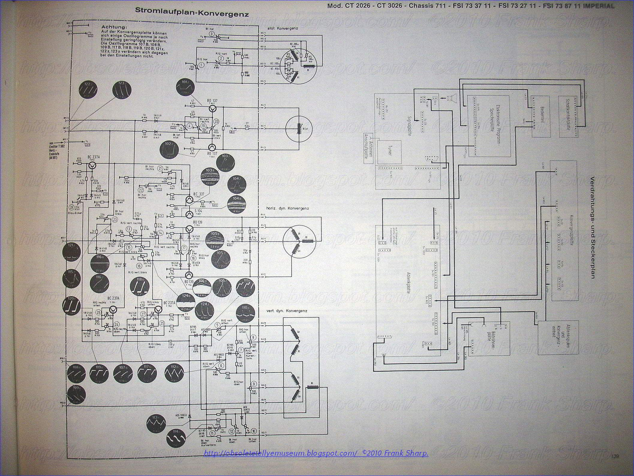
CHASSIS 711 (TELEFUNKEN).


IMPERIAL CT2026 CHASSIS 711 (TELEFUNKEN) power supply CONSTANT-VOLTAGE CONVERTER EMPLOYING THYRISTOR:
A constant voltage converter having a rectifier for rectifying AC power and with a thyristor connected between the rectifier and a filter for selectively passing therethrough a rectified output to an output terminal. There is a wave generator connected to the output of the rectifier for producing a first signal and an intergrator circuit connected to the output of the wave generator for producing an integral output in response to this first signal. In addition there is a detector circuit for detecting a fluctuation of the rectified output power and for producing second signal. A comparison circuit is connected between the intergrator circuit and the detector circuit for producing third signal in accordance with the comparison. A trigger circuit is connected between the comparison circuit and the control gate of the thyristor for supplying a phase control signal to the thyristor to thereby obtain a constant voltage output regardless of the fluctuation of the rectified output.
1. A constant voltage converter comprising an input of a power supply means, an output terminal, filter means, rectifier means connected to said input for rectifying a.c. power and for supplying output thereof to said output terminal, thyristor means connected between said rectifier means and said filter means for selectively passing therethrough a rectified output to the output terminal by way of said filter means, saw-tooth wave generator means connected between the output of said rectifier means and at least one integrator circuit means for producing an integral output in response to a saw-tooth wave produced, a first transistor in said saw-tooth wave generator, the input of said integrator circuit means being connected to a collector of said first transistor, detector circuit means connected to said output terminal for detecting a fluctuation of the rectified output power and for producing an output signal, said detector circuit means having a second transistor, pulse generator circuit means connected between said saw-tooth wave generator means and said detector circuit means for producing a trigger pulse to said thyristor through a trigger means, a third transistor in said pulse circuit generator means, the base of said third transistor being connected to the output of said integrator circuit means, the emitter thereof being connected to the emitter of said second transistor in said detector circuit means, and the collector thereof being connected to the gate of the thyristor means so as to supply a phase control signal thereto, thereby obtaining a constant voltage output regardless of the fluctuation of the rectified output.
Conventional constant-voltage converters of the type employing a thyristor are arranged to phase shift and full-wave-rectify an input a.c. power applied thereto and to maintain the output voltages constant by regulating the firing angle of the thyristor in comparison of the output voltages with the phase-shifted and rectified input a.c. power. When, however, these converters are connected to a common a.c. source having a relatively high internal impedance, the waveform of the phase-shifted and rectified a.c. input power is distorted thereby causing undesired operations of the converters.
It is therefore an object of the present invention to provide a constant-voltage converter which correctly operates notwithstanding the distortion of the input a.c. voltage.
Another object of the invention is to provide a constant-voltage converter which effectively suppress an undesired rush current.
Another object of the invention is to provide a constant-voltage converter having an improved feed-back circuit of a substantially constant loop gain .
In the drawings:
FIG. 1 is a schematic view of a converter according to the present invention;
FIG. 2 is a diagram showing a circuit arrangement of the converter of FIG. 1;
FIG. 3 is a diagram showing various waveforms of signals appearing in the circuit of FIG. 2;
FIG. 4 is a diagram showing various waveforms appearing in the circuit of FIG. 2 when an a.c. power is supplied to the circuit;
FIG. 5 is a diagram showing another circuit arrangement of the converter of FIG. 1;
FIG. 6 is a diagram showing waveforms of signals appearing in the circuit of FIG. 5; and
FIG. 7 is a diagram showing further another circuit arrangement of generator the of FIG. 1.
Referring now to FIG. 1, a cons
 tant-voltage
converter 10 according to the present invention comprises a
rectifier 11 having two input terminals 12 and 13 through which an
a.c. power is supplied. The rectifier 11 is preferably a full-wave
rectifier although a half-wave rectifier may be employed. An output
14 of the rectifier 11 is connected through a line 15 to an anode of a
thyristor 16. The thyristor 16 passes therethrough the rectified
a.c. power in only one direction from its anode to cathode when
triggered by a trigger pulse through its gate. The cathode of the
thyristor 16 is connected through a line 17 to an input of a smoothing
filter 18. The smoothing filter 18 smoothes the power from the
thyristor 16. An output of the smoothing filter 18 is connected
through a line 19 to an output terminal 20. The output 14 of the
rectifier 11 is also connected through a line 21 to a saw-tooth wave
generator 22 which generates a saw-tooth wave signal having the same
repetition period as the rectified input a.c. power. An output of
the saw-tooth wave generator 22 is connected through a line 23 to
one input of a trigger pulse generator 24. The other input of the
trigger pulse generator 24 is connected through a line 25 to the line
19. An output of the trigger pulse generator 24 is connected
through a line 26 to the gate of the thyristor 16. The trigger pulse
generator 24 produces a trigger pulse on its output when the
voltage of the saw-tooth wave signal reaches a level which is varied
in response to the output voltage on the terminal 20. The trigger
pulse generator 24 may be variously arranged and in this case
arranged to comprise rectangular generator 27 having one input
connected through the line 23 to the saw-tooth wave generator 22 and
the other input connected through a line 28 to an output voltage
detector 29. The detector 29 produces a reference signal
representing the output voltage on the terminal 20. The pulse
generator 27 is adapted to produces a rectangular pulse when the
saw-tooth wave signal to the one input reaches a level which defined
is in accordance with the reference signal. An output of the
rectangular pulse generator 27 is connected through a line 30 to an
input of a trigger circuit 31. The trigger circuit 31 is adapted to
convert the rectangular pulse into a spike pulse. An output of the
trigger circuit 31 is connected through the line 26 to the gate of
the thyristor 16.
tant-voltage
converter 10 according to the present invention comprises a
rectifier 11 having two input terminals 12 and 13 through which an
a.c. power is supplied. The rectifier 11 is preferably a full-wave
rectifier although a half-wave rectifier may be employed. An output
14 of the rectifier 11 is connected through a line 15 to an anode of a
thyristor 16. The thyristor 16 passes therethrough the rectified
a.c. power in only one direction from its anode to cathode when
triggered by a trigger pulse through its gate. The cathode of the
thyristor 16 is connected through a line 17 to an input of a smoothing
filter 18. The smoothing filter 18 smoothes the power from the
thyristor 16. An output of the smoothing filter 18 is connected
through a line 19 to an output terminal 20. The output 14 of the
rectifier 11 is also connected through a line 21 to a saw-tooth wave
generator 22 which generates a saw-tooth wave signal having the same
repetition period as the rectified input a.c. power. An output of
the saw-tooth wave generator 22 is connected through a line 23 to
one input of a trigger pulse generator 24. The other input of the
trigger pulse generator 24 is connected through a line 25 to the line
19. An output of the trigger pulse generator 24 is connected
through a line 26 to the gate of the thyristor 16. The trigger pulse
generator 24 produces a trigger pulse on its output when the
voltage of the saw-tooth wave signal reaches a level which is varied
in response to the output voltage on the terminal 20. The trigger
pulse generator 24 may be variously arranged and in this case
arranged to comprise rectangular generator 27 having one input
connected through the line 23 to the saw-tooth wave generator 22 and
the other input connected through a line 28 to an output voltage
detector 29. The detector 29 produces a reference signal
representing the output voltage on the terminal 20. The pulse
generator 27 is adapted to produces a rectangular pulse when the
saw-tooth wave signal to the one input reaches a level which defined
is in accordance with the reference signal. An output of the
rectangular pulse generator 27 is connected through a line 30 to an
input of a trigger circuit 31. The trigger circuit 31 is adapted to
convert the rectangular pulse into a spike pulse. An output of the
trigger circuit 31 is connected through the line 26 to the gate of
the thyristor 16.FIG. 2 illustrates a prefe
 rred
circuit arrangement of the converter shown in FIG. 1 which
comprises a rectifier 11 of a full-wave rectifier consisting of
rectifiers 40, 41, 42 and 43. Inputs of the rectifier are connected
to terminals 12 and 13 through which an a.c. power is applied. The
output 14 of the rectifier 11 is connected through a line 15 to an
anode of a thyristor 16. A cathode of the thyristor 16 is connected
through a line 17 to a smoothing filter 18 which includes a
capacitor C4 having one terminal connected to the line 17 and the
other terminal grounded. The output of the smoothing filter 18 is
connected through a line 19 to an output terminal 20.
rred
circuit arrangement of the converter shown in FIG. 1 which
comprises a rectifier 11 of a full-wave rectifier consisting of
rectifiers 40, 41, 42 and 43. Inputs of the rectifier are connected
to terminals 12 and 13 through which an a.c. power is applied. The
output 14 of the rectifier 11 is connected through a line 15 to an
anode of a thyristor 16. A cathode of the thyristor 16 is connected
through a line 17 to a smoothing filter 18 which includes a
capacitor C4 having one terminal connected to the line 17 and the
other terminal grounded. The output of the smoothing filter 18 is
connected through a line 19 to an output terminal 20.The rectangular pulse generator 27 comprises a transistor T 2 of PNP type having a base connected through a resistor R 6 to the collector of the transistor T 1 . An emitter of the transistor T 2 is connected through a resistor R 7 to the emitter of the transistor T 1 . A collector of the transistor T 2 is grounded through a resistor R 8 and connected through the line 30 to one terminal of a capacitor C 4 of the trigger circuit 31. The other terminal of the capacitor C 4 is connected through a line 26 to the gate of the thyristor 16.
The output voltage detector 29 includes a transistor T 3 of NPN type having an emitter grounded through a zener diode ZD. A collector of the transistor T 3 is connected through a line 28 to the emitter of the transistor T 2 and, on the other hand, connected through a capacitor C 5 to the grounded. A base of the transistor T 3 is connected to a tap of an adjustable resistor R 9 connected through a resistor R 10 and a line 25 to the line 19 and connected, in turn, to the ground through a resistor R 11 .
When, in operation, an a.c. electric power is applied through the input terminals 12 and 13 of the rectif
 ier
11, a full-wave rectified power as shown in FIG. 3 (a) appears on
the output 14. The rectified power is applied through the line 15 to
the anode of the thyristor 16. The thyristor 16 passes therethrough
the rectified power while its firing angle is regulated by the
trigger signal applied to the gate. The rectified power passed
through the thyristor 16 is applied through the line 17 to the
smoothing filter 18. The smoothing filter smoothes the power by
removing the ripple component in the power. The smoothed power
appears on the line 19 which is to be supplied to a load through the
output terminal 20. The smoothed power on the line 19 is, on the
other hand, delivered through the line 25 to the resistor R 10 of the output voltage detector 29. The resistor R 10 constitutes a voltage divider in cooperation with the resistors R 9 and R 11 . The output of the voltage divider is applied through the tap of the resistor R 9 to the base of the transistor T 3 . When the potential of the base of the transistor T 3 exceeds the zener voltage of the zener diode ZD, a base current flows through the transistor T 3 so as to render the transistor T 3 conductive. The potential of the collector of the transistor T 3
then varies in accordance with the voltage of the smoothed output
power on the line 19. The potential variation at the collector of the
transistor T 3 is then applied through the line 28 to
the trigger pulse generator 27 and utilized to regulate the
triggering timing of the thyristor 16.
ier
11, a full-wave rectified power as shown in FIG. 3 (a) appears on
the output 14. The rectified power is applied through the line 15 to
the anode of the thyristor 16. The thyristor 16 passes therethrough
the rectified power while its firing angle is regulated by the
trigger signal applied to the gate. The rectified power passed
through the thyristor 16 is applied through the line 17 to the
smoothing filter 18. The smoothing filter smoothes the power by
removing the ripple component in the power. The smoothed power
appears on the line 19 which is to be supplied to a load through the
output terminal 20. The smoothed power on the line 19 is, on the
other hand, delivered through the line 25 to the resistor R 10 of the output voltage detector 29. The resistor R 10 constitutes a voltage divider in cooperation with the resistors R 9 and R 11 . The output of the voltage divider is applied through the tap of the resistor R 9 to the base of the transistor T 3 . When the potential of the base of the transistor T 3 exceeds the zener voltage of the zener diode ZD, a base current flows through the transistor T 3 so as to render the transistor T 3 conductive. The potential of the collector of the transistor T 3
then varies in accordance with the voltage of the smoothed output
power on the line 19. The potential variation at the collector of the
transistor T 3 is then applied through the line 28 to
the trigger pulse generator 27 and utilized to regulate the
triggering timing of the thyristor 16.The full-wave rectified power is, on the other hand, applied through the line 21 to the saw-tooth wave generator 22. Since the resistors R 1 and R 2 consistute a voltage divider to reduce the voltage of the full-wave rectified power to a potential at the junction J 1 , a charging current to the capacitor C 1 flows from the emitter to the base of the transistor T 1 whereby the transistor T 1 repeats ON-OFF operation in accordance with the voltage of the rectified power. If the transistor T 1 is conductive when the voltage of the full-wave rectified power is lower than a threshold voltage v 1 as shown in FIG. 3(a), then the potential at the collector of the transistor T 1 is varied as shown in FIG. 3 (b) due to the charge and discharge of the capacitor C 2 . The variation of the potential at the collector of the transistor T 1 is supplied through the line 23 to the resistor R 6 of the trigger pulse generator 27.
As long as the voltage of the smoothed power on the line 19 equals to the rated output voltage, the transistor T 2 is adapted to become conductive when the voltage of the saw-tooth wave signal falls below a threshold value v 3 shown in FIG. 3(b). Therefore, a potential at the collector of the transistor T 2 varies as shown in FIG. 3(c). The potential variation, that is, a pulse signal at the collector of the transistor T 2 is supplied through the line 30 to the capacitor C 4 of the trigger circuit trigger 31. The trigger circuit 31 converts the pulse signal into a spike pulse or a trigger pulse shown in FIG. 3(d) which is then applied through the line 25 to the gate of the thyristor 16. Upon receiving the spike pulse, the thyristor 16 becomes conductive until the voltage of the rectified power on the line 15 falls below the cut-off voltage of the thyristor 16.
When the voltage of the smoothed power on the line 19 exceeds the rated output voltage, the collector current of the transistor T 3 increases with the result that the current flowing through the resistor R 7 increases. The threshold voltage of the transistor T 2 therefore reduces to a voltage v 2 as shown in FIG. 3(b). At this instant, leading edge of the pulse signal delays as shown by dot-and-dash lines in FIG. 3(c), so that each trigger pulse delays as shown by dot-and-dash line in FIG. 3(d). When on the contrary, the voltage of the smoothed signal on the line 19 lowers below the rated output voltage, the collector current of the transistor T 3 decreases whereby the threshold voltage rises to a voltage v 4 in FIG. 3(b). Each leading edge of the signal pulse now leads as shown by dotted line in FIG. 3(d). Being apparent from the above description, the appearance timing of each trigger pulse is regulated in accordance with the voltage of the smoothed power on the line 19 so that the voltage of the output voltage at the terminal 20 is held substantially constant.
Referring now to FIG. 4, start operation of the converte
 r
10 is discussed hereinbelow in conjunction with FIG. 2. When an
a.c. voltage is applied to the input terminals 12 and 13, the
capacitor C 3 begins to be charged by the voltage on the line 15, and the capacitor C 5 also begins to be charged through the resistors R 3 and R 7 . It is important that the time constant of power supply circuit constituted by the resistor R 3 and the capacitor C 3 is selected to be much larger than that of the time constant of another power supply circuit constituted by the resistor R 7 and the capacitor C 5 . Thus, the emitter potential of the transistor T 1 is built up more quickly than that of the transistor T 2 . Upon completion of the charging of the capacitor C 3 , the saw-tooth wave generator 22 begins to generate saw-tooth wave signal as shown in FIG. 4(b). Since the capacitor C 5 is, on the other hand, slowly charged, the emitter voltage of the transistor T 2 slowly rises as shown in FIG. 4(c), so that, the threshold voltage of the transistor T 2
gradually rises as shown by a dotted line in FIG. 4 (b).
Accordingly, the trigger pulses is produced on the gate of the
thyristor 16 as shown in FIG. 4(d), whereby the firing angle of the
thyristor 16 is gradually reduced as shown in FIG. 4(a) which
illustrates the voltage at the output terminal 14 of the rectifier
11. The output voltage on the output terminal 20 therefore gradually
rise up as shown in FIG. 4(e). It is to be understood that since the
output voltage of the converter 10 starts to gradually rise up as
shown in FIG. 4(e), an undesired rush current is effectively
suppressed.
r
10 is discussed hereinbelow in conjunction with FIG. 2. When an
a.c. voltage is applied to the input terminals 12 and 13, the
capacitor C 3 begins to be charged by the voltage on the line 15, and the capacitor C 5 also begins to be charged through the resistors R 3 and R 7 . It is important that the time constant of power supply circuit constituted by the resistor R 3 and the capacitor C 3 is selected to be much larger than that of the time constant of another power supply circuit constituted by the resistor R 7 and the capacitor C 5 . Thus, the emitter potential of the transistor T 1 is built up more quickly than that of the transistor T 2 . Upon completion of the charging of the capacitor C 3 , the saw-tooth wave generator 22 begins to generate saw-tooth wave signal as shown in FIG. 4(b). Since the capacitor C 5 is, on the other hand, slowly charged, the emitter voltage of the transistor T 2 slowly rises as shown in FIG. 4(c), so that, the threshold voltage of the transistor T 2
gradually rises as shown by a dotted line in FIG. 4 (b).
Accordingly, the trigger pulses is produced on the gate of the
thyristor 16 as shown in FIG. 4(d), whereby the firing angle of the
thyristor 16 is gradually reduced as shown in FIG. 4(a) which
illustrates the voltage at the output terminal 14 of the rectifier
11. The output voltage on the output terminal 20 therefore gradually
rise up as shown in FIG. 4(e). It is to be understood that since the
output voltage of the converter 10 starts to gradually rise up as
shown in FIG. 4(e), an undesired rush current is effectively
suppressed.FIG. 5 illustrates another fo
 rm
of the converter 10 which is arranged identically to the circuit
arrangement of FIG. 1 except that an integrator 50 is interposed
between the output of the saw-tooth wave generator 22 and the input
of the trigger pulse generator 27. The integrator 50 includes a
resistor R 12 having one terminal connected to the
output of the saw-tooth wave generator 22 and the other terminal
connected to the input of the rectangular pulse generator 27, and a
capacitor C 7 having one terminal connected to the other terminal of the resistor R 12 and the other terminal grounded.
rm
of the converter 10 which is arranged identically to the circuit
arrangement of FIG. 1 except that an integrator 50 is interposed
between the output of the saw-tooth wave generator 22 and the input
of the trigger pulse generator 27. The integrator 50 includes a
resistor R 12 having one terminal connected to the
output of the saw-tooth wave generator 22 and the other terminal
connected to the input of the rectangular pulse generator 27, and a
capacitor C 7 having one terminal connected to the other terminal of the resistor R 12 and the other terminal grounded.In operation, the saw-tooth wave generator 22 produces on its ouput a saw-tooth wave signal having decreasing exponential wave form portion as shown in FIG. 6 (a), although the saw-tooth wave signal ideally is illustrated in FIG. 3. This saw-tooth wave signal is converted by the integrator 50 into another form of saw-tooth wave having a increasing exponential wave form portion as shown in FIG. 6(b).
It should be noted that the saw-tooth wave signal of FIG. 6(a) has a smaller inclination near 180°. Hence, when the integrator 50 is omitted and the saw-tooth wave signal as shown in FIG. 6(a) is applied to the trigger pulse generator 27, the rate of change of the output voltage of the converter 10 become larger at a firing angle near to 1
 80°.
On the other hand, it is apparent from FIG. 6(c) that the rate of
change the output voltage of the thyristor 16 with respect to the
firing angle become large at a firing angle near to 180°. Therefore,
the loop gain of the trigger pulse generator 24 increases when the
firing angle of the thyristor 16 is near to 180°. It is apparent
through a similar discussion that the loop gain of the trigger pulse
generator 24 decreases when the firing angle is near to 90°. Such
non-uniformity of the loop gain of the trigger pulse generator invites a
difficulty of the regulation of the output voltage of the
converter. It is to be noted that the saw-tooth wave signal shown in
FIG. 6(b) has a large inclination at an angle near 180°. Therefore,
when the saw-tooth wave signal of FIG. 6(b) is applied to the
trigger pulse generator 24, the loop gain of the trigger pulse
generator 24 is held substantially constant, whereby the output
voltage of the converter is effectively held constant.
80°.
On the other hand, it is apparent from FIG. 6(c) that the rate of
change the output voltage of the thyristor 16 with respect to the
firing angle become large at a firing angle near to 180°. Therefore,
the loop gain of the trigger pulse generator 24 increases when the
firing angle of the thyristor 16 is near to 180°. It is apparent
through a similar discussion that the loop gain of the trigger pulse
generator 24 decreases when the firing angle is near to 90°. Such
non-uniformity of the loop gain of the trigger pulse generator invites a
difficulty of the regulation of the output voltage of the
converter. It is to be noted that the saw-tooth wave signal shown in
FIG. 6(b) has a large inclination at an angle near 180°. Therefore,
when the saw-tooth wave signal of FIG. 6(b) is applied to the
trigger pulse generator 24, the loop gain of the trigger pulse
generator 24 is held substantially constant, whereby the output
voltage of the converter is effectively held constant.It is to be understood that the integrator 50 may be substituted for by a miller integrator and a bootstrap integrator. Furthermore, a plurality of integrator may be employed, if desired.
FIG. 7 illustrates another circuit arrangement of the converter according to the present invention, which is arranged identically to the circuit of FIG. 2 except for the trigger circuit 31 and the smoothing circuit 18.
The trigger circuit 31 of FIG. 7 comprises a transformer TR with primary and secondary coils. One terminal of the primary coil is connected to the resistor R 7 of the pulse generator 27. The other terminal of the primary coil is connected to a collector of a transistor T 4 of NPN type. The secondary coil has terminals respectively connected to the gate and cathode of the thyristor 16. An emitter of the transistor T 4 is grounded through a resistor R 13 . A base of the transistor T 4 is grounded through a resistor R 14 and connected through a capacitor C 8 to the collector of the transistor T 2 of the pulse generator 27.
The smoothing filter 18 of FIG. 7 comprises a choke coil CH connected to the lines 17 and 19, and to capacitors C 9 and C 10 which are in turn grounded. The circuit of FIG. 7 operates in the same manner as the circuit of FIG. 2.
Obviously many modifications and variations of the present invention are possible in the light of the above teachings. It is therefore to be understood that within the scope of the appended claims the invention may be practiced otherwise than as specifically described.
The CRT TUBE IS a TELEFUNKEN A66-140X.
E/W CORRECTION Circuit arrangement in an image display apparatus for (horizontal) line deflection:
Line deflection circuit in which the deflection coil is east-west modulated. In order to cancel an east-west dependent horizontal linearity defect the inductance value of the linearity correction coil is made independent of the field frequency, for example by means of a compensating current. In an embodiment this current is supplied by the shunt coil of the east-west modulator.
1. Circuit arrang
ement for use with a line deflection coil, said circuit comprising a generator means adapted to be coupled to said coil for producing a sawtooth line-deflection current through said line deflection coil, said deflection current having a field-frequency component current, a horizontal linearity correction coil adapted to be coupled in series with said deflection coil and including an inductor having a bias-magnetized core, and means for making the inductance value of the linearity correction coil substantially independent of the field frequency component current. 2. Circuit arrangement as claimed in claim 1, wherein said making means includes a current supply source means for producing a compensating line-frequency sawtooth current through a winding of the linearity correction coil, the amplitude of the compensating current having a field-frequency variation. 3. Circuit arrangement as claimed in claim 2, wherein the direction of curvature of the field-frequency envelope of the compensating current is opposite to the direction of curvature of the field-frequency component current of the line deflection current, whereby the magnetic fields produced in the core of the correction coil by the two currents have the same direction. 4. Circuit arrangement as claimed in claim 2, wherein the direction of curvature of the field-frequency envelope of the compensating current is the same as the direction of curvature of the field-frequency component current of the line deflection current, whereby the magnetic fields produced in the core of the correction coil by the two currents have opposite directions. 5. Circuit arrangement as claimed in claim 2, wherein said correction coil further comprises an additional winding disposed on the core, said additional winding being coupled to said supply source means to receive the compensating current. 6. Circuit arrangement as claimed in claim 5, further comprising modulator means for modulating the line deflection current with said field frequency component, said modulator including a compensation coil coupled in series with said additional winding. 7. Horizontal linearity correction coil comprising a core made of a magnetic material and bias-magnetized by at least one permanent magnet, and an additional winding disposed on the core. 8. Image display apparatus including a circuit arrangement as claimed in claim 1.
y correction coil the linearity error due to the ohmic resistance of the deflection circuit is corrected. The sign of the bias magnetisation is chosen so that it is cancelled by the deflection current at the beginning of the deflection interval, so that the inductance of the correction coil is a maximum, whereas the voltage drop across the deflection coil then is a minimum. This voltage drop is adjustable by adjustment of the starting inductance of the correction coil. During the deflection interval the core gradually becomes saturated so that the inductance of, and the voltage drop across, the correction coil decrease. Thus the linearity error can be cancelled exactly at the beginning of the interval, that is to say on the left on the screen of the image display tube, and with a certain approximation at other locations.
was found in practice that the said two corrections are not independent of one another, that is to say the adjustment of the east-west modulation affects horizontal linearity. As long as the modulation depth is not excessive, a satisfactory compromise can be found. However, in display tubes having a deflection angle of 110° and particularly in colour display tubes in which the deflection coils have a converging effect also, it is difficult to find such a compromise. A tube of this type is described in "Philips Research Reports," volume Feb. 14, 1959, pages 65 to 97; the distribution of the deflection field is such that throughout the display screen the landing points of the electron beams coincide without the need for a converging device. Owing to this field distribution, however, the pin-cushion-shaped distortion in the image displayed in the east-west direction is greater than in comparable display tubes of another type. Hence there must be east-west modulation of the line deflection current to a greater depth. It is true that under these conditions horizontal linearity can correctly be adjusted over a given horizontal strip after the east-west modulation has been adjusted correctly, i.e., for a rectangular image, but it is found that in other parts of the display screen a serious linearity error remains. When vertical straight lines are displayed as straight lines in the right-hand part of the screen, they are displayed as curved lines in the left-hand part.
 simplified circuit diagram of a line deflection circuit of an
image display apparatus, not shown further. The circuit includes
the series combination of a line deflection coil L y , a linearity correction coil L and a trace capacitor C t , which series combination is traversed by the line deflection current i y . The collector of an npn switching transistor T r and one end of a choke coil L 1 are connected to a junction point A of a diode D, a capacitor C r
and the said series combination. The other end of the choke coil
is connected to the positive terminal of a supply voltage source
which supplies a substantially constant direct voltage V b
and to the negative terminal of which the emitter of transistor
Tr is connected. This negative terminal may be connected to earth.
The other junction point B of elements D and C r and of the series combination of elements C t , L y
and L is connected to one terminal of a modulation source M for
east-west correction which has its other terminal connected to
earth. Diode D has the pass direction shown in the FIG.
simplified circuit diagram of a line deflection circuit of an
image display apparatus, not shown further. The circuit includes
the series combination of a line deflection coil L y , a linearity correction coil L and a trace capacitor C t , which series combination is traversed by the line deflection current i y . The collector of an npn switching transistor T r and one end of a choke coil L 1 are connected to a junction point A of a diode D, a capacitor C r
and the said series combination. The other end of the choke coil
is connected to the positive terminal of a supply voltage source
which supplies a substantially constant direct voltage V b
and to the negative terminal of which the emitter of transistor
Tr is connected. This negative terminal may be connected to earth.
The other junction point B of elements D and C r and of the series combination of elements C t , L y
and L is connected to one terminal of a modulation source M for
east-west correction which has its other terminal connected to
earth. Diode D has the pass direction shown in the FIG.  ottom left-hand part of FIG. 3 flows through the coil, the field strength H varies proportionally about the value H 0 ,
for the mean value of the current is zero. Because the curve of L
is not linear, the variation L(t) of L, which is shown in the top
right-hand part, is not a linear function of time. The resulting
curve may be regarded as composed of a linear component and a
substantially parabolic component which is to be taken into account
when choosing the capacitance of capacitor C t .
ottom left-hand part of FIG. 3 flows through the coil, the field strength H varies proportionally about the value H 0 ,
for the mean value of the current is zero. Because the curve of L
is not linear, the variation L(t) of L, which is shown in the top
right-hand part, is not a linear function of time. The resulting
curve may be regarded as composed of a linear component and a
substantially parabolic component which is to be taken into account
when choosing the capacitance of capacitor C t . . The amplitude of current i 2 and the turns number of winding L 2 can be chosen so that current i y flows through inductances the total value of which is not dependent upon the field frequency. The curve L(t) of FIG. 3 remains substantially unchanged. Consequently the undesirable field-frequency modulation is removed without variation of the bias magnetization, which would have been varied if current i 2 were a field-frequency current. Obviously the same result can be achieved by a choice such of the direction of current i 2 and of the winding sense of winding L 2 that the two field strengths are subtracted one from the other, whilst the curvature of the envelope of current i 2 has the same direction as that of the envelope of current i y .
 C' t . One end of winding L 2 is connected to the junction point of capacitor C' t and the coil L, whilst the other end is connected to earth via coil L'. The capacitances of capacitors C 1 and C 2 and the location of the tapping on coil L 1 are chosen so that the sawtooth currents flowing through L y , and L' and L 1
have the same retrace time, whilst the field-frequency linearity
defect of FIg. 2 is cancelled by correctly proportioning winding L
2 .
C' t . One end of winding L 2 is connected to the junction point of capacitor C' t and the coil L, whilst the other end is connected to earth via coil L'. The capacitances of capacitors C 1 and C 2 and the location of the tapping on coil L 1 are chosen so that the sawtooth currents flowing through L y , and L' and L 1
have the same retrace time, whilst the field-frequency linearity
defect of FIg. 2 is cancelled by correctly proportioning winding L
2 . NORD SOUTH (NORD/SUD) CORRECTION CIRCUIT ARRANGEMENT FOR CORRECTING THE DEFLECTION OF AT LEAST ONE ELECTRON BEAM IN A TELEVISION PICTURE TUBE BY MEANS OF A TRANSDUCTOR :
A circuit arrangement for raster correction in a television picture tube by means of a transductor whose power winding is connected in parallel with at least a portion of the line deflection coils, the line deflection genera
 tor
having a low internal impedance. In order to increase this
impedance a mainly inductive impedance is connected in series with
the generator. In a picture tube employing at least two electron
beams the series impedance may include the convergence circuit. As a
result the convergence in the corners of the picture screen is
also improved. The linearity control circuit may likewise form part
of the series impedance.
tor
having a low internal impedance. In order to increase this
impedance a mainly inductive impedance is connected in series with
the generator. In a picture tube employing at least two electron
beams the series impedance may include the convergence circuit. As a
result the convergence in the corners of the picture screen is
also improved. The linearity control circuit may likewise form part
of the series impedance.1. A deflection circuit for a cathode ray tube comprising a transistor horizontal deflection generator; a horizontal deflection coil parallel coupled to said generator; means for pincushion correction of said tube comprising a saturable reactor having a control winding adapted to receive a vertical deflection signal and a power winding parallel coupled to at least a portion of said deflection coil; and means for increasing the effectiveness of said correction means comprising an impedance element external to said generator having a substantially inductive reactance series coupled between said generator and said coil. 2. A circuit as claimed in claim 1 wherein said generator comprises a transformer having a tap and said power winding has a first end coupled to said coil and a second end coupled to said tap. 3. A circuit as claimed in claim 1 wherein said impedance element comprises means for controlling the linearity of the beam deflection. 4. A deflection circuit for a cathode ray tube having at least two electron beams comprising a transistor horizontal deflection generator; a horizontal deflection coil parallel coupled to said generator; means for pincushion correction of said tube comprising a saturable reactor having a control winding adapted to receive a vertical deflection signal and a power winding parallel coupled to at least a portion of said deflection coil; means for increasing the effectiveness of said correction means comprising an Impedance element external to said generator having a substantially inductive reactance series coupled between said generator and said coil; and means for dynamically converging said beams comprising a convergence circuit coupled to said horizontal generator and to said transductor. 5. A circuit as claimed in claim 4 wherein said generator comprises a transformer having a tap and said power winding has a first end coupled to said coil and a second end coupled to said tap. 6. A circuit as claimed in claim 4 wherein said impedance element comprises means for controlling the linearity of the beam deflection.
A circuit arrangement for raster correction with the aid of a transductor is described, for example, in U.S. Pat. No. 3,444,422. In this patent the power winding of a transductor is connected in parallel with the horizontal deflection coils while the control winding receives a signal of field frequency so that the current of line frequency which flows through the deflection coils is modulated at the field
-frequency (East-West correction), whereas the vertical deflection current is modulated at the line frequency (North-South correction). However, in this known arrangement there is the difficulty that the transductor can exert little influence on the horizontal deflection current if the internal impedance of the deflection generator is low because the transductor then only constitutes an additional load on the generator. This is the case when the deflection generator includes a valve with feedback -- or a switch formed with one or more transistors. In order to be able to use a transductor arrangement also in such a case the circuit arrangement according to the invention is characterized in that a mainly inductive impedance is connected in series between the said parallel arrangement and the deflection generator.
Due to the step according to the invention the internal impedance of the deflection generator is increased and the different components of the circuit remain mainly inductive so that the deflection current is more or less linear when the voltage provided by the deflection generator during the line scan period is substantially constant. The series impedance may be, for example, a fixed coil. However, the invention is furthermore based on the recognition of the fact that the increase in the internal resistance of the horizontal deflection generator may not only be obtained by a constant impedance, but other arrangements envisaging other improvements of the deflection may be used for this purpose. In that case even special improvements may be obtained as will be apparent hereinafter and possible small non-linearities of the additionally used arrangements have no detrimental results.
It is true that in known convergence circuits in picture tubes employing a plurality of electron beams a satisfactory improvement is obtained for the central horizontal and vertical lines of a picture tube of the shadow mask type. However, it is found that convergence errors may subsist in the corners of the picture. Known circuit arrangements which correct these second-order errors are often complicated and expensive. In the circuit arrangement according to the invention a satisfactory compensation of such convergence errors is possible in a simple manner if the series impedance which is arranged between the horizontal deflection generator and the deflection coils includes the convergence circuit. In this manner the sum of the deflection current and of the current derived for the field correction and modulated by the transductor flows through the convergence circuit so that the desired additional convergence correction in the corners of the written raster is obtained.
In order that the invention may be readily carried into effect a few embodiments thereof will now be described in detail by way of example with reference to the accompanying diagrammatic drawings in which:
FIG. 1 shows a circuit arrangement in which the transductor is connected in parallel with the deflection coils, while in
FIG. 2 the transductor is only fed by part of the voltage applied to the deflection coils.
FIG. 1 shows two line-output transistors 1 and 2 which are arranged in series. The emitter of transistor 2 is connected to ground through a winding 3 while the collector of transistor 1 is connected through a winding 4 and a small series impedance 5, preferably a resistor, to the positive terminal of a supply source V b whose negative terminal is connected to ground.
Windings 3 and 4 are wound together with
an EHT-winding 6 on the same transformer core 7. The ends of
windings 3 and 4 remote from each other are connected through the
capacitor 10 for the S-correction to the deflection-unit consisting
of two windings 8 and 9 arranged, for example, in parallel. The
base of transistors 1 and 2 receive pulses of line frequency in a
manner not shown in FIG. 1 so that these transistors are cut off
during the flyback period. During the scan period, a substantially
constant voltage is applied to the deflection unit. Consequently a
more or less sawtooth-shaped current flows through windings 8 and
9. The bipartite power winding 11 of a transductor ensuring the
raster correction is connected in parallel with this deflection
unit 8, 9. The control winding 12 of said transductor, and a
converting capacitor 13 in parallel therewith form part of the
circuit for the vertical deflection through terminals 14 and 15. An
adjustable coil 16 with which the raster correction can be
adjusted exactly is connected in series with winding 12.Windings 3 and 4 have the same number of turns so that pulses of the same amplitude and reversed polarity are produced at the emitter of transistor 2 and at the collector of transistor 1. As a result a disturbing radiation of these pulses is reduced. Furthermore, transistor types are chosen in this Example for transistors 1 and 2 whose collector-base diodes may function as efficiency diodes. All this has been described in U.S. Pat. No. 3,504,224.
According to the invention the convergence circuit 17 is arranged through a separation transformer 20 between the end of winding 3 remote from winding 4 and the horizontal deflection coils 8, 9. Furthermore, this current branch includes the linearity control circuit 21 which comprises the parallel arrangement of a resistor and a coil whose inductance is adjustable, for example, by means of premagnetization of the core of the coil. A current, which is the sum of the current for the deflection coils 8, 9 and of the current for the power winding 11 of the transductor, flows through the primary winding of transformer 20. This primary current is transformed to the secondary circuit of transformer 20 so that a current flows through convergence circuit 17.
In known arrangements the con
vergence current is only influenced by the deflection current itself. It has been found that in this case the convergence correction is not sufficient in the corners of the picture. At these areas, where the deflection in both directions is at a maximum, a greater intensity of the convergence current is required. This is especially the case in picture tubes having a great deflection angle and according to the invention this is achieved in that the current which is derived from the power winding 11 of the transductor for the raster correction is also applied to the convergence circuit. This current flows from the horizontal deflection generator constituted by windings 3 and 4 through the primary winding of transformer 20 to power winding 11 of the transductor. The transductor current is in fact at a minimum in the center of the picture and increases towards the edges and particularly towards the corners. Thus the convergence current varies in the desired manner. According to the invention the desired improvements of the convergence correction and simultaneously the likewise desired increase in the internal resistance of the horizontal deflection generator is consequently obtained without a considerable increase in the number of required circuit elements and without disturbing the normal operation of the circuit arrangement. Due to transformer 20 a terminal of convergence circuit 17 may be connected to ground so that the convergence can be adjusted safely. If necessary, a suitable impedance transformation may also be obtained with the aid of transformer 20.
The linearity control circuit 21 may alternatively be connected in series with the said branch which includes transformer 20. As a result the internal resistance of the horizontal deflection generator for the line frequency is further increased without the field correction and the convergence correction being disturbingly influenced.
FIG. 2 shows a modification of the circuit arrangement according to the invention in which the deflection current is not changed relative to that of FIG. 1. The end of power winding 11 of the transductor shown on the upper side of FIG. 1 is connected to ground in FIG. 2. In addition convergence circuit 17 is included between winding 3 and ground so that separation transformer 20 may be omitted. If as a first approximation the impedances 5 and 17 are assumed to be negligibly small relative to the other impedance of the circuit arrangement, power winding 11 may be considered to be connected to a tap on the deflection generator 3, 4. Consequently, only approximately half the voltage of the deflection generator is applied to transductor winding 11 which winding must
therefore be proportioned in such a manner that it can convey a
current which is approximately twice as large as that of FIG. 1.
This larger current also flows through convergence circuit 17
which, with the omission of separation transformer 20, is
favorable for the convergence in the corners of the picture screen.In FIG. 2 the emitter of transistor 2 is connected to ground i.e., the said tap on the deflection generator. During the scan period the series arrangement of supply source V b and windings 3 and 4 FIG. 1 is substantially short-circuited by transistors 1 and 2. In order that these transistors in the circuit arrangement according to FIG. 2 operate under the same circumstances as those in FIG. 1, an additional winding 24 must be wound on core 7 between windings 4 and 6, winding 24 having the same number of turns as winding 3, and the collector of transistor 1 must be connected to the junction of windings 6 and 24.
The end of power winding 11 connected to ground in FIG. 2 may alternatively be connected for the desired adjustment of the corner convergence to a different tap on the transformer, that is to say, on winding 3 or 4.
Resistor 5 serves in known manner mainly as a safety resistor so that in case of an inadmissible load of the EHT, for example, as a result of flash-over in the picture tube, the supply voltage for transistors 1 and 2 is reduced so that overload of these transistors is avoided.

Circuit arrangement for establishing a reference potential of a chassis of an electrical device such as a radio and/or TV receiver, such device being provided with at least one contactless touching switch operating under the AC voltage principle. The device is switched by touching a unipole touching field in a contactless manner so as to establish connection to a grounded network pole. The circuit arrangement includes in combination an electronic blocking switch and a unidirectional rectifier which separates such switch from the network during the blocking phase.
 1.
A circuit arrangement for establishing, at the chassis of an
electrical device powered by a grounded AC supply network, a
reference potential with relation to ground, said device having
at least one contactless touching switch operating on the AC
voltage principle, the switch being operated by touching a
unipole touching field in a contactless manner, said arrangement
comprising an electronic switch for selectively blocking the
circuit of the device from the supply network, a half-wave
rectifier including a pair of diodes individually connected in
series-aiding relation between the terminals of the supply network
and the terminals of the device for separating the electronic
blocking switch from the supply network during a blocking phase
defined by a prescribed half period of the AC cycle, and a pair of
condensers individually connected in parallel with the respective
diodes. 2. A circuit
arrangement according to claim 1, wherein the capacitances of the
two condensers are of equal magnitude.
1.
A circuit arrangement for establishing, at the chassis of an
electrical device powered by a grounded AC supply network, a
reference potential with relation to ground, said device having
at least one contactless touching switch operating on the AC
voltage principle, the switch being operated by touching a
unipole touching field in a contactless manner, said arrangement
comprising an electronic switch for selectively blocking the
circuit of the device from the supply network, a half-wave
rectifier including a pair of diodes individually connected in
series-aiding relation between the terminals of the supply network
and the terminals of the device for separating the electronic
blocking switch from the supply network during a blocking phase
defined by a prescribed half period of the AC cycle, and a pair of
condensers individually connected in parallel with the respective
diodes. 2. A circuit
arrangement according to claim 1, wherein the capacitances of the
two condensers are of equal magnitude.
In electronic devices, for example TV and radio receivers, there are used in ever increasing numbers electronic touching switches for switching and adjusting the functions of the device. In one known embod
 iment
of this type of touching switch, which operates on a DC voltage
principle, the function of the electronic device, is
contactlessly switched by touching a unipole touching field, the
switching being carried out by means of an alternating current
voltage. When using such a unipole touching electrode, one takes
advantage of the fact that the AC current circuit is generally
unipolarly grounded. In order to close the circuit by touching the
touching surface via the body of the operator to ground, it is
necessary to provide an AC voltage on the touching field. In one
special known embodiment there is employed a known bridge current
rectifier for the current supply. This type of arrangement has the
drawback that the chassis of the device changes its polarity
relative to the grounded network pole with the network frequency.
With such construction considerable difficulties appear when
connecting measuring instruments to the device, such difficulties
possibly eventually leading to the destruction of individual
parts of the electronic device.
iment
of this type of touching switch, which operates on a DC voltage
principle, the function of the electronic device, is
contactlessly switched by touching a unipole touching field, the
switching being carried out by means of an alternating current
voltage. When using such a unipole touching electrode, one takes
advantage of the fact that the AC current circuit is generally
unipolarly grounded. In order to close the circuit by touching the
touching surface via the body of the operator to ground, it is
necessary to provide an AC voltage on the touching field. In one
special known embodiment there is employed a known bridge current
rectifier for the current supply. This type of arrangement has the
drawback that the chassis of the device changes its polarity
relative to the grounded network pole with the network frequency.
With such construction considerable difficulties appear when
connecting measuring instruments to the device, such difficulties
possibly eventually leading to the destruction of individual
parts of the electronic device.In order to avoid these drawbacks, the present invention provides a normal combination of a unidirectional rectifier with an electronic blocking switch that separates the chassis of the electronic device from the network during the blocking phase. In accordance with the present invention, the polarity of the chassis of the electronic device does not periodically change, because the electronic device is practically separated from the network during the blocking phase of the unidirectional rectifier by means of the electronic blocking switch.
In a further embodiment of the invention a further rectifier is connected in series with the unidirectional rectifier in the connection between the circuit and the negative pole of the chassis. Such further rectifier is preferably a diode which is switched in the transfer direction of the unidirectional rectifier. According to another feature of the invention there are provided condensers, a respective condenser being connected parallel with each of the rectifiers. Preferably the two condensers have equal capacitances. Because of the use of such condensers, which are required because of high frequency reasons, during the blocking phase there is conducted to the chassis of the electronic device an AC voltage proportional to the order of capacitances of the condensers. Thus there is placed upon the touching field in a desired manner an AC voltage, and there is thereby assured a secure functioning of the adjustment of the device when such touching occurs.
I
n
the embodiment of the invention employing two rectifiers there
is the further advantage that over a bridging over of the minus
conduit of the rectifier that is connected between the network
and the negative pole of the chassis connection, no injuries can
be caused by a measuring instrument in the electronic device
itself and in the circuit arrangement connected thereto.In the accompanying drawing:
The sole FIGURE of the drawing is a circuit diagram of a preferred embodiment of the invention.
In the illustrated embodiment the current supply part of the device, shown at the left, is connected via connecting terminals A and B to an AC voltage source, the terminal B being grounded at 8. The current supply part consists of a unidirectional rectifier in the form of a diode 1 with its anode connected to the terminal I, the cathode of diode 1 being connected to one input terminal 9 of an electronic device 2. In the device 2 there is also arranged a sensor circuit 3, shown here mainly as a block, circuit 3 being shown as including a pnp input transistor the emitter of which is connected to an output terminal 11 of the device 2. The collector of such transistor is connected to the other output terminal 12 of the device 2. The base of the transistor is connected by a wire 13 to a unipolar touching field 4 which may be in the form of a simple metal plate instead of the pnp transistor shown, the sensor circuit itself may consist of a standard integrating circuit which controls, among other things, the periodic sequential switching during the touching time of the touching field 4. All of the circuits of the electronic device 2 are isolated in a known manner from the chassis potential. Between the network terminal B and the negative pole 10 of the chassis there is arranged in the direction opposite that of diode 1 a further diode 5, the anode of diode 5 being connected to the terminal 10, and the cathode of diode 5 being connected to the terminal B of the current supply. To provide for HF type bridging of the diodes 1 and 5 there are arranged condensers 6 and 7 respectively, which are connected in parallel with such diodes.
The invention functions by reason of the fact that in an AC network separate devices radiate electromagnetic waves which produce freely traveling fields in the body of the person who is operating and/or adjusting the device, thereby producing an alternating current through his body to ground, as indicated by the - line at the right of the circuit diagram. If now the person operating the device touches the switching field 4, then the pnp type input transistor of the sensor circuit 3, which is placed on a definite reference potential (for example 12 Volts) and is connected with the negative halfwave of the AC voltage potential, is made conductive. There is thereby released a control command in the sequential switching, for example, for switching the electronic device to the next receiving channel. It is understood that the most suitable connection is formed between ground and the touching field 4 by means of a wire. By the use of such wires it would be assured that in all cases the base of the transistor in circuit 3 is connected to ground. This would, however, not permit anyone to operate the switch without the use of an auxiliary means such as a wire. It will be assumed that the touching almost always results directly via the almost isolated human body. For this reason the AC current fields are necessary, because otherwise there cannot always be provided a ground contact. Thus this connection is established via the body resistance of the person carrying out the touching of the switch.
The
positive half wave of the alternating current travels to the
terminal 9 of the electronic device 2 after such current has been
rectified and smoothed by the devices 1, 6. Such positive
halfwave is also conducted to the sensor circuit 3. The thus
formed current circuit is closed by way of the chassis of the
electronic device 3, the diode 5, and the terminal B. When there is a
negative halfwave of the alternating current delivered by the
current supply, both diodes 1 and 5 remain closed so that the
chassis of the device 2 remains separated from the network during
the blocking phase. Nevertheless, by means of condensers 6 and 7
the chassis is placed in a definite network potential, which
depends on the relationship of the order of magnitude of the two
condensers 6 and 7. When the capacitances of such condensers are
equal, there is placed upon the chassis of the device 2 the
constant reference potential, and simultaneously there is present
via the sensor circuit 3 the required AC voltage at the touching
field 4 for adjusting the function or functions of the device 2
upon the touching of the touching field 4.The reference character 15 indicates a terminal or point at which the potential of the chassis of the device 2 may be measured. As above explained, the diode 5 causes the potential of the chassis at 15 to be separated from the network ground when a negative AC halfwave arrives. It will be noted that the return conduit of the circuit is held at a fixed chassis potential. The input transistor of the sensor circuit 3 remains, however, locked because it is subjected to a DC current of about 12 volts. If now, by means of touching the touching field 4, the chassis potential is connected to ground, then the transistor switches through and releases a switching function.
A suitable sensor which may be employed for the circuit 3 herein may be a sensor known as the "SAS 560 Tastatur IS," manufactured and sold by Siemens AG.
It is to be understood that the present invention is not limited to the illustrated environment. They can also be used in electronic blocking switch including a Thyristor circuit, which in the same manner separates the electronic device during the blocking phase from the network rectifier. With such Thyristor circuit the drawbacks described in the introductory portion of the specification of known circuit arrangements are also avoided.
Although the invention is illustrated and described with reference to a plurality of preferred embodiments thereof, it is to be expressly understood that it is in no way limited to the disclosure of such a plurality of preferred embodiments, but is capable of numerous modifications within the scope of the appended claims.
IMPERIAL CT2026 CHASSIS 711 (TELEFUNKEN) COLOR BURST CIRCUIT WITH A.G.C.
1. A circuit comprising: means for receiving a color television signal having amplitude varying color information and burst signal components, means coupled to said receiving means for separating said components from said television signal, a burst signal path coupled to said separating means for receiving only said burst signal, said path comprising the serial coupling of means for passively regenerating a subcarrier reference signal from said burst signal, means having a control terminal for controlling the amplitude of said subcarrier reference signal within said burst signal path without effecting the amplitude of said color information signals, means for detecting the amplitude of the output of said amplitude controlling means
and a high pass filter coupled between said detecting means and said control terminal; whereby said reference signal is kept at a substantially constant amplitude regardless of the rapidity of said variations. 2. A circuit as claimed in claim 1 further comprising a chrominance amplifying means for amplifying both said color information and burst signal components and means for controlling the gain of said chrominance amplifier coupled to the output of said detecting means. 3. A circuit as claimed in claim 2 where
 in
said chrominance signal amplifier-controlling means comprises a
low-pass filter having a higher cutoff frequency than said
high-pass filter.
in
said chrominance signal amplifier-controlling means comprises a
low-pass filter having a higher cutoff frequency than said
high-pass filter. In known receivers of the above-mentioned type the drawback occurs that particularly upon reception of weak signals the color subcarrier reference signal may show great fluctuations as a result of the burst signal decreasing in amplitude sometimes during a number of successive line periods. This reference signal is used for synchronously demodulating the color difference signals which are passed through the color information signal. Upon variation in the amplitude of the reference signal this may give rise to color errors upon this demodulation. Consequently, to prevent this phenomenon a limiter stage is generally included after the passive integrator. However, this limiter does not operate at a slight amplitude of the integrated burst signal. The operation of this limiter may be rendered more effective by using more amplification stage for this limiter. From an economic point of view this is, however, not particularly interesting. An object of the invention is to avoid as must as possible the occurrence of color errors upon reception of weak signals.
According to the invention a color television receiver of the type described in the preamble is characterized in that the said output of the detection circuit is connected through a low cutoff filter to a gain-control input of an amplifier included in the burst signal path outside the color information signal path.
As a result an automatic gain control is obtained which acts upon comparatively rapid variation in the amplitude of the regenerated color subcarrier reference signal and which tends to maintain the amplitude of this reference signal constant. By the step according to the invention this rapid automatic gain control is not effective in the color information signal path. This is based on the recognition of the fact that due to the short duration of the burst signals amplitude variation often occur in the individual bursts, which variation are not representative of the amplitude variations which occur in the associated line periods in the color information signal. Any automatic gain control for the color information signal path obtained from the burst signal path must therefore not be influenced by accidental fluctuations of the burst signal amplitude, such as occur particularly upon reception of weak signals.
In order that the invention may be readily carried into effect it will now be described in detail, by way of example, with reference to the accompanying diagrammatic drawing which shows a color television receiver according to the invention in a block diagram.
Details which are not important for the understanding of the invention have been omitted as much as possible for the sake of clarity.
In the Figure, a section of the receiver is indicated by 1 in which a color television signal receiver through an input 3 is amplified and converted into a brightness signal Y, a chrominance signal 1 Chr and a synchronization signal S. These signals occur at the outputs 5, 7 and 9, respectively, of the section 1.
The output 5 of the section 1 is connected to an input 11 of a picture display section 13. The brightness signal Y is applied through this line to the picture display section 13.
The output 7 of the section 1 is connected to an input 15 of a chrominance amplifier 17. An output 19 of the chrominance amplifier 17 is connected to an input 21 of a separator stage 23. The separator stage 23 further has an input 25 which is connected to an output 27 of a time base state 29, through which line it is possible to apply a switching signal to the separator stage 23.
The time base stage 29 receives a synchronization signal S from an input 31 connected to the output 9 of the section 1 and supplies time base currents to the picture display section 13 through an output 33 which is connected to an input 35 of the picture display section 13.
The chrominance signal Chr becoming available at the output 7 of the section 1 comprises a color information signal and a burst signal. The color information signal is applied from the output 7 through the chrominance amplifier 17 and the separator stage 23 to an output 37 thereof and the burst signal is applied from the output 7 through the chrominance amplifier 17 and the separator stage 23 to an output 39 of this stage. To this end a time selection is applied on the chrominance signal in the separator stage 23 with the aid of a switching signal applied to the input 25.
The output 37 is connected to an input 41 of a color information signal amplifier 43. An output 45 thereof is connected to an input 47 of a demodulator and matrix circuit 49. The demodulator and matrix circuit 49 has three outputs 51, 53 and 55 which are connected to inputs 57, 59 and 61, respectively, of the picture display section 13.
The signal path leading from the output 7 of the section 1 through the chrominance amplifier 17, the separator stage 23, the output 37 of this separator stage, the color information amplifier 43 to the input 47 of the demodulator and matrix circuit 49 belongs to the color information signal path. The color information signal is applied through this path to the demodulator and matrix circuit 49.
The output 39 of the separator stage 23 is connected to an input 63 of a burst signal amplifier 65. An output 67 of the burst signal amplifier 65 is connected to an input 69 of a passive integrator circuit 71 and to an input 73 of a phase detection circuit 75. The passive regenerator is a high-Q crystal circuit. This circuit along with the phase detector and their operation are described in "Proceedings of the I.R.E.," Jan. 1954, vol. 42, pp. 111--112.
The
color subcarrier burst are integrated to form a continuous
reference signal with the aid of the passive integrator circuit 71.
This reference signal becomes available at the output 77. The
output 77 is connected to an input 79 of a reference signal
amplifier 81. A reference signal which is applied to an input 85 of
the demodulator and matrix circuit 49 becomes available at an
output 83 of this amplifier.The reference signal is further applied to an input 87 of the phase detection circuit 75. The phase of the burst signal applied through the input 73 is compared in the phase detection circuit 75 with that of the integrated burst signal (reference signal) applied through the input 87. A voltage which is a measure of the phase deviation between these two signals is obtained at an output 89. The output 89 is connected to the input 91 of the passive integrator circuit 71. A phase deviation possibly produced in the integrator circuit 71 is corrected with the aid of the voltage applied through this line, so that the phase of the reference signal obtained at the output 83 is maintained as much as possible the same as that of the burst signal applied to the input 69.
The reference signal obtained at the output 83 is further applied to a detection circuit having a diode 92, a capacitor 93 and a resistor 95. A voltage dependent on the amplitude of the reference signal is obtained from an output 97 of the detection circuit 92, 93, 95. This voltage is applied through a low-pass filter serving as a high cutoff filter including a resistor 99 and a capacitor 101 to a gain control input 103 of the chrominance amplifier 17. The gain of the chrominance amplifier 17 is thus dependent on the average amplitude of the burst signal. This average amplitude is thus maintained substantially constant. The average amplitude of the burst signal is a measure of the amp
litude of the color information signal. Hence the color information signal appears with a automatically corrected amplitude at the output 19 of the chrominance amplifier 17. The saturation of a picture obtained with the aid of the color information signal will thus be substantially independent of variations in the transmission of the transmission path of the color television signal.
The above described trajectory from the output 7 of the section 1 through the chrominance amplifier 17, the output 39 of the separator stage, the burst signal amplifier 65, the passive integrator circuit 71, the reference signal amplifier 81 and the detection circuit 92, 93 95 belongs to the burst signal path. Part of the burst signal path, namely the chrominance amplifier 17, coincides with part of the color information signal path.
According to the invention the output 97 of the detection circuit 92, 93, 95 provided in the burst signal path is connected through a high-pass filter serving as a low cutoff filter, including a capacitor 105 and a resistor 107, to a gain control input 109 of an amplifier 81 included outside the color information signal path. Rapid variations in the output signal of the reference signal amplifier 81 will be readjusted by the automatic gain control circuit thus formed without exerting influence on the color information signal path.
According to the invention this rapid automatic gain control, which is effected outside the color information signal path, is based on the recognition of the fact that rapid variations in the amplitude of the burst signal such as occur, for example, upon reception of weak signals or during the frame flyback period, are no measure of the variations in the color information signal and hence must not exert influence on a possible automatic gain control in the color information signal path.
By the step according to the invention a very constant reference signal voltage amplitude is obtained at the input 85 of the demodulator and matrix circuit 49 so that it will substantially be impossible for color errors to occur due to the demodulation of the color information signal, even with unfavorable conditions of reception.
The
lower limit frequency of the high-pass filter 105, 107 is preferably chosen to be such that it is higher than the upper limit frequency of the low-pass filter 99--101.
It will be evident that the rapid automatic gain control according to the invention can be used in color television receivers for both the NTSC-system and the PAL-system.
Although the described embodiment includes a control voltage from the output 97 of the detection circuit 92, 93, 95 to the input 103 of the chrominance amplifier 17. It is readily evident that this voltage is not essential for using the step according to the invention. However, to ensure a satisfactory operation of the color difference signal demodulators it is generally desirable to apply this control voltage to the input 103.
In the embodiment described the feedback of the rapid automatic gain control is effected in the reference signal amplifier 81 following the passive integrator circuit 71. The feedback may in principle also be effected in an amplifier, for example, preceding the passive integrator circuit or, at will, preceding as following it.
A color television receiver includes conventional circuitry for processing and detecting a received color television signal. Three chrominance-luminance matrices combine detected color difference and luminance signals forming color red, blue and green video signals. Emitter follower coupling stages apply the color video signals individually to each
of three output amplifiers which in turn drive the cathode electrodes of a unitized gun CRT. Potentiometers couple the emitter electrodes of the output amplifiers to a source of operating potential providing a simultaneous signal gain and DC output voltage adjustment for each amplifier during CRT color temperature setup. A voltage divider controls the voltage applied to the common screen grid electrode of the CRT providing a master setup adjustment.
1. In a color televison receiver, for processing and displaying a received television signal bearing modulation components of picture information, having a cathode ray tube including a trio of electron source means producing individual electron beams impinging an image screen to form three substantially overlying images and in which the respective operating points and relative conduction levels of said electron source means determine the color temperature of the reproduced image, the combination comprising:
master conduction means, coupled to said trio of electron source means simultaneously varying said conduction levels;
a plurality of substantially equal bandwidth amplifiers, each coupled to a different one of said electron source means, separately influencing said conduction levels;
low output impedance signal translation means recovering said picture information and supplying it to each of said plurality of amplifiers; and
separate adjusting means individually coupled to at least two of said amplifiers for simultaneously producing predetermined same sense variations in gain and DC output voltage of its associated amplifier while preserving said bandwidths.
2. The combination set forth in claim 1, wherein the transconductance and cutoff voltage of each of said electron source means bear a predetermined relationship and wherein said simultaneous predetermined variations in gain and DC output voltage are determined by said transconductance-cutoff voltage relationship. 3. The combination set forth in claim 2, wherein said plurality of amplifiers each include a gain and DC output voltage determining impedance and wherein each of said separate adjusting means include:
a variable impedance, coupling said gain and DC output voltage determining impedance of said associated amplifier to a source of bias current and forming a shunt path for signals within said amplifier.
4. The combination set forth in claim 3, wherein each of said electron source means include a cathode electrode and wherein each of said amplifiers include:
a transistor having input, common, and output electrodes, said output electrode being coupled to said electron source means cathode.
5. The combination set forth in claim 4, wherein said gain and DC output voltage determining impedance is coupled to said common electrode. 6. The combination set forth in claim 5, wherein said input, common, and output electrodes of said transistors are defined by base, emitter, and collector electrodes, respectively. 7. The combination set forth in claim 6, wherein said gain and DC output voltage determining impedance includes a resistor coupling said emitter electrode to ground and wherein said variable impedance includes:
a resistive control, having a variable resistance, coupling said emitter electrode to a source of operating potential.
8. The combination set forth in claim 7, wherein said three electron source means include control grid and screen grid electrodes common to said three electron guns and wherein variations of cathode electrode voltages permit changes of said relative conduction levels and said respective operating points. 9. The combination set forth in claim 8, wherein said master conduction means includes a variable bias potential source coupled to said common screen grid electrode.
This invention relates to color television receivers and in particular to cathode ray tubes (CRT) drive systems therefor. Each of the several types of color television cathode ray tubes in current use includes a trio of individual electron sources producing distinct electron beams which are directed toward an image screen formed by areas of colored-light-emitting phosphors deposited on the inner surface of the CRT. The phosphors emit light of a given additive primary color (red, blue or green) when struck by high energy electrons. A "delta" electron gun arrangement, in which the electron sources comprise three electron guns disposed at the vertice
s of an equilateral triangle, having its base oriented in a horizontal plane and its apex above or below the base plane, may be used. Alternatively, the three electron sources may be "in line", that is, positioned in a horizontal line. In either case, the three beams produced are subjected to deflection fields and scan the image screen in both the horizontal and vertical directions thereby forming three substantially overlying rasters.
The phosphor deposits forming the image screen may alternatively comprise round dots, elongated areas, or uninterrupted vertical lines. A parallax barrier or shadow mask, defining apertures generally corresponding to the shape of the phosphor areas, is interposed between the electron guns and the image screen to "shadow" or block each phosphor area from electrons emitted from all but its corresponding electron gun.
A color television signal includes both luminance (monochrome) and chrominance (color) picture components. In the commonly used RGB drive systems the separately processed luminance and chrominance information is matrixed (or combined) before application to the CRT cathodes. Three output amplifiers apply the respective red, blue and green video signals thus produced for controlling the respective electron source currents.
The luminance components have substantially the same effect on all three electron sources whereas the color components are differential in nature, causing relative changes in electron source currents. In the absence of video signals, the combined raster should be a shade of grey. At high gun currents, the grey is very near white and at low settings, it is near black. The "color", commonly called color temperature, of the monochrome raster depends upon the relative contributions of red, blue and green light. At high color temperatures, the raster may appear blue and at low color temperatures it may appear sepia. While the most pleasing color temperature is largely a matter of design preference, ideally the receiver should not change color temperature under high and low brightness nor for high and low frequency picture information.
Generally, the electron sources comprise individual electron guns each including separately adjustable cathode, control grid and screen grid electrodes and a desired color temperature is achieved by adjustment of each electrode voltage during black and white setup. While the exact setup procedure employed varies with the manufacturer and specific CRT configuration, all manufacturers attempt to achieve consistent color temperature throughout the usable range of CRT beam current variations.
A typical color temperature adjustment involves setting the low light color temperature condition of each electron gun by adju
 sting
its screen grid electrode voltage to produce the required DC
conditions between electron guns at minimum beam currents. A high light
or dive adjustment at increased CRT beam current is then made to
insure consistent color temperature. In receivers utilizing CRT's with
separately adjustable screen grid electrode voltages, the drive
adjustment may take the form of a minor change in signal gain of the
output amplifiers. The process is, in essence, one of configuring the
operating points of the three electron guns to conform to three
substantially identical output amplifiers.
sting
its screen grid electrode voltage to produce the required DC
conditions between electron guns at minimum beam currents. A high light
or dive adjustment at increased CRT beam current is then made to
insure consistent color temperature. In receivers utilizing CRT's with
separately adjustable screen grid electrode voltages, the drive
adjustment may take the form of a minor change in signal gain of the
output amplifiers. The process is, in essence, one of configuring the
operating points of the three electron guns to conform to three
substantially identical output amplifiers.The recently developed economical "unitized gun" type CRT has a combined electron source structure in which three common control grids and three common screen grids are used with the cathodes being the only electrically separate electrodes. The greatly simplified and more economical unitized gun structure, however, imposes some restrictions on the circuitry used to drive the electron sources. Perhaps most significant is the absence of
the flexibility previously provided by individually adjustable screen grid electrode voltages. Due in part to the inverse relationship between electron source transconductance, which may be thought of as "gain" of the electron source, and cutoff voltage, the typical individual low level color temperature or equal cutoff adjustment described above also performs the additional function of establishing nearly equal transconductances for the three electron sources. As a result only minor relative changes in electron source currents occur at higher CRT beam currents.
Color temperature adjustment in a receiver with a unitized gun CRT involves a somewhat different process, namely, configuring the drive and bias applied to each of the gun cathodes to accommodate differences in relative electron source characteristics which, without the equalizing effect of separate screen electrode adjustments, may be considerable.
Initially television receivers using unitized gun CRT's utilized a variable DC voltage divider operative upon each output amplifier to provide adjustment of the DC cutoff voltage. Drive, or signal gain, adjustment to accommodate differences in electron source transconductances was generally accomplished by separate individual gain controls operative on each of the output amplifiers.
However, the more recently developed unitized gun systems combine the DC voltage (cutoff) and signal gain (drive) adjustments for each electron source by simultaneously varying the signal gain and DC voltage in the same direction in a predetermined relationship. One such system used three CRT coupling networks each of which includes a variable impedance simultaneously operative on both the amplitude of coupled signal and DC voltage. Another system uses a variable collector load impedance for each of the output amplifiers, making use of the changes in amplifier signal gain and DC output voltage resulting from collector load variations.
While such systems provide an adequate range of adjustment to achieve color temperature setup using a reduced number of controls, they often degrade image quality. Ideally, the luminance portion of the signal is applied uniformly to each of the three electron sources. Although the relative signal amplitudes may be varied to accommodate transconductance differences between electron sources, it is desirable that each applied signal be an otherwise identical replica of the others. The variable impedance elements in the voltage divider networks and variable collector loads of the prior art interact with the capacities inherent in the output amplifiers and electron gun structures to produce unequal bandwidths for the different color video signals, which cause color changes in their high frequency components (which correspond to detailed picture information). The resulting effect upon the displayed image is similar in appearance to the well-known "color fringing" or misconvergence effect.
OBJECTS OF THE INVENTION
It is an object of the present invention to provide an improved color television receiver.
It is a further object of this invention to provide a novel CRT color temperature setup system.
SUMMARY OF THE INVENTION
In a color television receiver, for processing and displaying a received television signal bearing modulation components of picture information, a
cathode ray tube includes three electron source means producing individual electron beams which impinge an image screen to form three substantially overlying images. The respective operating points and relative conduction levels of the electron source means determine the color temperature of the reproduced image. Master conduction means, coupled to the three electron source means, simultaneously vary the conduction levels and a plurality of substantially equal bandwidth amplifiers, each coupled to a different one of the electron source means, separately influence the conduction levels. Low output impedance signal translation means recover the picture information and supply it to each of the amplifiers. Separate adjusting means are individually coupled to at least two of the amplifiers for simultaneously producing predetermined variations in the gain and DC output voltage of the amplifiers while preserving the bandwidths.
BRIEF DESCRIPTION OF THE DRAWING
The drawing shows a partial-schematic, partial-block diagram representation of a color television receiver constructed in accordance with the present invention.
DESCRIPTION OF THE PREFERRED EMBODIMENT
Referring to the drawing, a signal processor 10 includes conventional circuitry (not shown) for amplifying a received television signal and detecting
the
modulated components of luminance and chrominance information therein.
The output of signal processor 10 is coupled to a luminance amplifier
11 and a chrominance processor 30. Luminance amplifier 11 is
conventional and includes circuitry controlling brightness and contrast
of the luminance signal. The output of luminance amplifier 11 is
coupled to three luminance-chrominance matrices 12, 13 and 14.
Chrominance processor 30 includes conventional chrominance information
detection circuitry for providing three color difference or
color-minus-luminance output signals (R-Y, G-Y and B-Y) which are
individually coupled to luminance-chrominance matrices 12, 13 and 14,
respectively. The signal from luminance amplifier 11 is combined with
the color-minus-luminance signals from chrominance processor 30 to form
the respective red, green and blue video signals which are coupled to
the R, G and B output amplifiers 15, 16 and 17, respectively. The
outputs of amplifiers 15, 16 and 17 are coupled to the cathode
electrodes 23, 24 and 25, respectively, of a CRT 20 having an image
screen 21. A voltage divider, formed by a series combination of
resistors 83 and 84, is coupled between a source of operating potential
+V2 and ground. The junction of resistors 83 and 84 is
connected to a common control grid electrode 28 and to ground by a
filter capacitor 85 which provides a signal bypass. A potentiometer 80
and a resistor 81 are series coupled between a source of operating
potential +V1 and ground, forming another voltage divider.
The junction of potentiometer 80 and resistor 81 is connected to common
screen grid electrode 29 and to ground by a bypass capacitor 82.
Cathode electrodes 23-25, control grid electrode 28 and screen grid
electrode 29 are part of a unitized gun structure in CRT 20 with the
control grid and screen grid being common to each of the three electron
sources defined by the separate cathode electrodes.While luminance-chrominance matrices 12 and 13 are shown in block form, it should be understood that they are identical to the detailed structure of matrix 14. Similarly, red output amplifier 15 and green output amplifier 16 are identical to the detailed structure of blue output amplifier 17. Further, the receiver shown is understood to include conventional circuitry for horizontal and vertical electron beam deflection together with means deriving a CRT high voltage accelerating potential, all of which have, for clarity, been omitted from the drawing.
Luminance-chrominance matrix 14 includes a matrix transistor 40 having an emitter electrode 41 coupled to ground by a resistor 55 and by a series combination of resistors 46 and 47, a base electrode 42 coupled to the output of luminance amplifier 11, and a collector electrode 43 coupled to a source of operating potential +V3 by a resistor 45. The B-Y output of chroma processor 30 is connected to the junction of resistors 46 and 47. An emitte
r-follower transistor 50 has an emitter electrode 51 coupled to ground by a resistor 56, a base electrode 52 connected to the collector of matrix transistor 40, and a collector electrode 53 connected to +V3.
Blue amplifier 17 includes an output transistor 60 having an emitter electrode 61 coupled to ground by a series combination of resistors 67 and 68, a base electrode 62 connected to the emitter of transistor 50, and a collector electrode 63 coupled to +V2 by a resistor 66. A series combination of a potentiometer 70 and a resistor 69 couples the junction of resistors 67 and 68 to +V3. Collector 63, which is the output of amplifer 17, is connected to cathode 25 of CRT 20.
During signal reception, the separately processed luminance and B-Y color difference signals are applied to matrix transistor 40. The combi
ned
signal developed at its collector 43 forms the blue video signal which
controls the blue electron beam in CRT 20 and represents the relative
contribution of blue light in the image produced.The blue video signal at collector 43 is coupled via transistor 50 to base 62 of output transistor 60. The low source impedance of emitter follower transistor 50 obviates any detrimental effects upon the blue video signal due to loading at the input to amplifier 17 caused by gain or frequency dependent input impedance variations of amplifier 17. The blue video signal applied to base 62 is amplified by transistor 60 to a level sufficient to control the conduction of its respective electron source.
During color temperature setup, a predetermined setup voltage (corresponding to black) is applied to matrices 12, 13 and 14. The voltage on common screen grid electrode 29 is adjusted, by varying potentiometer 80 which together with resistor 81 and capacitor 82 form master conduction means, to cause a low brightness raster to appear on image screen 21. As will be seen, adjustment of potentiometer 70 and the corresponding potentiometers in amplifiers 15 and 16 establish the correct combination of DC electron source cathode voltages and output amplifier gains to produce the selected color temperature at both low and high CRT beam currents.
Amplifier 17 includes a common emitter transistor stage in which the impedance coupled to emitter electrode 6 is a gain and DC output voltage determining impedance. Signal gain is approximately equal to the ratio of the collector impedance (resistor 66), to this gain and DC voltage determining impedance (ignoring the effects of capacities associated with the tr
ansistor and the electron gun which will be considered later). Because the source of operating potential +V3 coupled to potentiometer 70 forms a good AC or signal ground, the series combination of resistor 69 and potentiometer 70 are effectively in parallel with resistor 68 and the total impedance coupling emitter 61 to signal ground comprises resistor 67 in series with this combination of resistors 68 and 69 and potentiometer 70. Variations in this impedance caused by adjustment of potentiometer 70 changes the ratio of collector to emitter impedances and thereby the gain of amplifier 17. If potentiometer 70 is varied to present increased resistance, gain is reduced and if varied to present decreased resistance, gain is increased.
The DC voltage at collector 63 of transistor 60 is determined by the product of the collector resistance and quiescent collector current (current in the absence of applied signal) and V2. The voltage at base 62 is established by the emitter voltage of transistor 50. Variations in the resistance of potentiometer 70 cause variations in current flow in the series path including potentiometer 70 and resistors 69 and 68. The voltage developed across resistor 68 is supplied to emitter 61 through resistor 67.
In the absence of signal, the DC voltage at base 62 is constant and the relative voltage between base 62 and emitter 61, which controls the conduction level of transistor 60, is a function of the voltage at emitter 61. Increases in the resistance of potentiometer 70 reduce the emitter voltage, increase the relative base-emitter voltage of transistor 60, and increase collector current. The increased collector current develops a greater voltage drop across collector resistor 66 and reduces the DC voltage at collector 63 (and cathode 25). Conversely, a decrease in the resistance of potentiometer 70 increases the voltage at emitter 61, reducing the relative base-emitter voltage and decreasing collector current. The smaller voltage drop across resistor 66 increases the DC voltage at collector 63 and cathode 25.
Thus, increasing the resistance
of
potentiometer 70 produces proportionate simultaneous reduction of the
DC voltage applied to cathode 25 and the voltage gain of amplifier 17,
whereas decreasing the resistance of potentiometer 70 produces
proportionate simultaneous increase of the DC voltage and signal gain.
As mentioned above, amplifiers 15 and 16 are identical to amplifier 17.
In practice only two of the three output amplifiers require adjustment
to achieve color temperature setup. However, greater flexibility and
optimum use of amplifier signal handling capability is realized if all
three output amplifiers are adjustable.As previously mentioned capacities associated with transistor 60, cathode 25 and corresponding interconnections (such as those used to couple collector 63 to cathode 25) are effectively in parallel with collector load resistor 66 forming a partially reactive "coupling network" which exhibits a frequency characteristic (bandwidth) affecting signals coupled therethrough. In practice, the other coupling networks have identical bandwidths and affect their signals in an equal manner. The setup control adjustments of the present invention do not change the characteristics of these coupling networks and the uniformity of signal coupling for the different color signals is preserved. In contrast, conventional adjustment circuitry (whether variable collector load or voltage divider) place variable impedances within these couplings. The varied adjustments of these impedances to effect color temperature control adjustment disturb the bandwidth characteristics of the coupling networks causing differential variations in the individual color video signals.
What has been shown is an RGB CRT drive system which includes output amplifiers each having a single control which simultaneously achieves changes of the DC output voltage and signal gain of the amplifier in a predetermined relationship. The bandwidths of all three output amplifiers and their associated coupling networks remain substantially undisturbed by these control adjustments during CRT color temperature setup.
While particular embodiments of the invention have been shown and described, it will be obvious to those skilled in the art that changes and modifications may be made without departing from the invention in its broader aspects, and, therefore, the aim in the appended claims is to cover all such changes and modifications as fall within the true spirit and scope of the invention.
p.In order to demodulate the PAL chrominance subcarrier it is known to delay the chrominance subcarrier by one picture line period in a glass ultrasound delay line and to add, to the delayed chrominance subcarrier in successive adder stages, the undelayed chrominance subcarrier and the undelayed chrominance subcarrier which has been shifted in phase by 180°, respectively. This produces a split of the signal into the two carrier frequency components (R-Y) and (B-Y). The (B-Y) component is demodulated in a first demodulator with the use of a reference carrier generated by a reference carrier oscillator and the (R-Y) component, whose phase alternates from line to line by 180°, is demodulated in a second demodulator with the use of a reference carrier which has been shifted by 90° and is switched by 180° from line to line. In this way the two video frequency color difference signals (B-Y)' and and (R-Y)' are produced which constitute an average over two lines. This manner of decoding has the drawback that a glass delay line is required which cannot be integrated in modern semiconductor circuits.
The periodical Funk-Technik, 1971, No. 6, at pages 195-198, discloses the use of two bucket brigade circuits in the PAL decoder instead of a glass delay line. Since the bucket brigade circuits have the characteristic of a lowpass filter, they can be used only to delay video frequency signals. For that reason, the known decoder splits the chrominance subcarrier by means of two synchronous demodulators into the two video frequency signals (B-Y) and (R-Y). These signals are then delayed by one picture line period in a delay line designed as a shift register for analog signals. By adding the two undelayed signals to the correponding delayed signals, the two color difference signals (B-Y)' and (R-Y)' are generated in an adder stage. Thereafter the two color difference signals (B-Y)' and (R-Y)' are fed, in a given ratio, to a further adder stage serving as matrix which generates the color difference signal (G-Y)' therefrom. This decoder had the drawback that it requires a large number of structural components.
TBA950-2 TBA950-2 Television Signal Processing CircuitGeneral Description
The T B A 9 5 0 - 2 is a monolithic integrated circuit for pulse separation and line synchronization in T V receivers
w i t h transistor o u t p u t stages.
The TBA950 comprises the sync separator with noise suppression, the frame pulse integrator, the phase comparator, a switching stage for automatic changeover of
noise immunity, the line oscillator w i t h frequency range limiter, a phase control circuit and the o u t p u t stage.
It delivers prepared frame sync pulses for triggering the frame oscillator. The phase comparator may be switched
for video recording operation. Due t o the large scale of integration, few external components are needed.


The TBA530 is an integrated R - G - B matrix
pre-amplifier for colour television receivers incorporating a matrix pre-amplifier for R—G—B cathode or grid drive of
the picture tube without clamping circuits. The chip layout has been designed to ensure tight thermal coupling between
all transistors in each channel t o minimise thermal drifts between channels. Also, each channel follows an identical
layout t o ensure equal frequency behaviour of the three channels.
This integrated circuit has been designed to be driven from the TBA520 synchronous demodulator integrated
circuit.


1. Output load resistor, red Signal (pin 11: blue signal, pin 14: green signal) Resistors (47 kQ, 1 W) connected to +200 V provide the high value loads for the internal amplifying stages . .The nominal operating potential on these pins is defined by an internal zener type junction and the d. c. feedback and is approximately +8 V. The maximum current which can be allowed at each of these pins is 10ma.
2. R - Y input signal
This signal is fed via a low-pass filter from the TBA520 demodulator i. c. (pin 7) having a d. c. level of +7.5 V and an amplitude of /1. 4~ V peak to peak. The input resistance for this pin is typically 60 kOHM an input capacitance of less than 3 pF (similarly for pins 3 and 4).
3. G- Y input signal
The d. c. black level of this signal is +7.5 V and its amplitude is O. 82 V peak to
peak (see pin 2).
4. B- Y input signal
The d. c. 'black level of this signal is +7.5 V and its amplitude is,!. 78' V peak to
peak (see pin 2) ,
5. Luminance signal input
The d. c. level on this pin for picture black is +1.5 V. The required signal amplitude is 1 V black-to-white with negative-going sync (or blanking) for cathode
drive as shown. The input resistance at this pin is 20 kohm approximately with a capacitance of typ. 10 pF.
6. Negative supply (earth)
7. Current feed point A current of approximately 2.5 ma is required at this pin, fed via a 3.9 kQ resistor from +12 V, to bias the internal differential amplifiers. A decoupling capacitor of 4. 7 nF is necessary.
8. Positive 12 V supply Maximum supply voltage permitted, 13.2 V; Current consumption approximately 30 ma.
9. Blue channel feedback (green channel, pin 12: red channel, pin 15) The d. c. working points and gains of both the output stages and the i. c.amplifier stages are stabilised by the feedback circuits. The black level potentials at the collectors of the output stages (tube cut-off) are adjusted by setting correctly the d. c. level of the colour difference signals produced by the TBA520 demodulator i. c. The gains of the R -G-B output stages are adjusted to give the correct white points setting on the picture tube by adjusting the potentiometers in the feedback paths (VR1, VR2). (See notes on setting up decoder).
10. Blue signal output (green and red signal outputs on 13 and 16) These pins cire internally connected with pins 11, 14 and 1 respectively via zener type junctions to give a d. c. level shift appropriate for driving the output transistor bases directly. To by-pass the zener junctions at h. f. three 10 nF ca- pacitors are required.
11. Output load resistor, blue channel (pin 1).
12. Green channel feedback (see pin 9).
13. Green Signal output (see pin 10).
14. Output load resistor , green channel (see pin 1).
15. Red channel feedback (see pin 9).
16. Red signal output (see pin 10).
BRIEF PERFORMANCE DETAILS AND COMMENTS
1. Spread of the ratio of voltage -gains for colour difference and luminance signal inputs' O. 9 to 1. 1.
2. Very careful attention to earth paths should be given, avoiding common impedances between the input (decoder) side and the output stages. Also, to enable matched performance to be achieved, a symmetrical board and component layout should be adopted for the three output stages. To compensate for the effect upon h. f. response of inevitable differences, e. g. , the absence of a potentiometer in one of the stages, the compensating capacitors Cl' C2 and C3 may be appropriately selected for any given board layout.
3. The signal black level at the collectors of the R -G- B output stages depends upon the +12 V supply, the d. c. level of the colour difference signals from the TBA520 demodulator i. c. and the black level potential of the luminance signal applied to the TBA530 matrix i. c. The d. c. levels of the signals produced and handled by the i. c. 's are designed to have approximately proportional tracking with the 12 V supply potential,
To ensure that changes in picture black level due to variations on the 12 V supply to the i. c. 's occur in a predictable way, all the 1. c. 's should be operated from a common supply line. This is specially important for the TBA520 and TBA530. Furthermore, to limit the changes in picture black level during receiver operation, the 12 V supply should have a stability of not worse than ±3% due to operational variations. and preferably be tracked with the screen - grid supply of the picture tube.
TBA540 REFERENCE COMBINATION:


The TBA540 is an integrated reference oscillator circuit for colour television receivers incorporating an automatic phase and amplitude controlled oscillator employing a quartz crystal, together with a half -line frequency synchronous demodulator circuit. The latter compares the phases and amplitude of the swinging burst ripple and the PAL flip-flop waveform, and generates appropriate a. c. c., colour killer and identification signals. The use of synchronous demodulation for these functions permits a high standard of noise immunity.
The function is quoted against the corresponding pin number
1. Oscillator feedback output The crystal receives its energy from this pin. The input impedance is approximately 2 kQ in parallel with 5 pF.
2. Reactance control stage feedback
This pin is fed internally with a sine wave derived from the reference input (pin 6) and controlled in amplitude by the internal reactance control circuit~ The phase of the feedback from pin 2 to the crystal via C 1 is such that the value of C 1 is ef- fectively increased. Pin 2 is held internally at a very low impedance therefore the tuning of the crystal is controlled automatically by the amplitude of the feedback waveform and its influence on the effective value of C 1. 3. Positive 12V supply The maximum voltage must not exceed 13.2 V.
4. Reference waveform output
This pin is driven internally by the regenerated sub carrier waveform in R-Y phase. An output amplitude of nominally 1. 5 V peak-to-peak is produced at low impedance. No d. c.load to earth is required. A d. c. connection between pins 4 and 6 is, how- ever, necessary via the bifilar coupling inductor. The function of this inductor is to produce, on pin 6, a signal of equal amplitude and opposite phase (-(R-Y» to that on pin 4. A centre tap on the inductor, connected to earth vil:j. a d.c. block- ing capacitor, is therefore necessary.
5. Burst waveform input
A burst waveform amplitude of 1 V peak-to-peak is required to be a. c. -coupled to this pin. The amplitude of the burst will normally be controlled by the adjust- ment and operation of the a. c. c. circuit. The input impedance at this pin is approximately 1 kQ and a threshold level of 0.7 V must be exceeded before the burst signal becomes effective. A d. c. bias of 400 mV is internally derived for pin 5 The absolute level of the tip of the burst at pin 5 will normally reach 1. 25 V (1. 5 V peak-to-peak burst amplitude). Under abnormal conditions the burst amplitude should not be allowed to exceed 3 V peak-to-peak and a limiting condition will be . reached in the 1. c. which inhibits the performance of the phase lock loop.
6. Reference waveform input This pin requires a reference waveform in the -(R-Y) phase, derived from pi4 via a bifilar transformer (see pin 4), to drive the internal balanced-reactance control stage. A d. c. connection between pIns 4 and 6 must be made via the transformer.
7.. Colour killer output
This pin is driven from the collector of an internal switching transistor and requires an external load resistor (typical 10 kg) connected to +12 V. The unkilled and killed voltages on this pin are then +12 V and < 250 mV respectively.
(The voltage on pin 9 at which switching of the colour killer output on pin 7
occurs is nominally +2. 5 V
8. P. A. L. flip-flop square wave input A 2.5V peak -to -peak square wave derived from the P.A.L. flip-flop (in the TBA520 demodulator i. c. ) is required at this pin, a. c. -coupled via a capacitor. The input impedance is about 3.3 kQ.
9. A.C.C. output An emitter follower provides a low impedance output potential which is negative going with a rising burst input amplitude. With zero input signal the d. c. potential produced at pin 9 is set to be +4 V (RVl) The appearance of burst signal on pin 5 will cause the potential on pin 9 to go in a negative direction in the event that the P. A. L. flip-flop is identified to be in the correct phase. The range of potential over which full a. c. c. control is excercised at pin 9 is deter- mined by the control characteristics of the a.c.c. amplifier . for the TBA560 from 1 V to 0.2 V. The potential at pin 9 will fall to a value within this range as the burst input signal is stabilised at 1. 5 V peak-to-peak. The latter condition is achieved by correct adjustment of RV2. If, however, the P.A.L. flip-flop phase is wrong the potential on pin 9 will move positively. The potential divider RS, R6 will then operate a P.A.L. switch cut-off function in the TBA520 demodulator i. c. The· switching of the colour killer output at pin 7 is designed to occur as the potential on pin 9 moves past +2. 5 V.
'10. A.C.C. level setting
The network connect~d between pins 10 and 12 balances the a.c.c. circuit and RV1 is adjusted to give +4 V on pin 9 with no burst input signal to pin 5. C5 provides filtering.
11. A.C.C. gain control RV2 is adjusted to give the correct amplitude of burst signal on pin 5 (1. 5 V peak- -to-peak) under a. c. c. control;
12. See pin 10.
13: See pin 14.
14, D. C. control points in reference control loop Pins 13 and 14 are connected to opposite sides of a differential amplifier cir- cuit and are brought out for the purposes d. c. balancing of the reactance stage and the connection of the bandwidth-determining filter network. The convention- al double time constant filter networks are R2, C2, R3, C3 and R4' C4' The d. c. potentials on these pins are nominally +7, 2 V.
15. Oscillator feedback input The input impedance at this pin is nominally 3.5 k:Q in parallel with 5 pF. No d. c. connection is required on this pin. The voltage in the i. c. between pin 15 and pin 1 is nominally 4. 7 times.
16. Negative supply (earth)
PERFORMANCE AND COMMENTS
Initial adjustment
(a) Remove burst signal.
(b) Short-circuit pins 13-14. Adjust oscillator to correct frequency by C 1. Remove
short circuit.
(c) Set the a. c. c. level adjustment RV 1, to give +4 V on pin 9.
(d) Apply burst signal.
(e) Adjust a. c. c. gain, RV 2, to give a burst amplitude of 1. 5 V peak-to-peak on pin 5.
Phase 'lock loop performance (with crystal type 4322 152 0110)
(a) Phase difference between reference and burst signals for ±400 Hz deviation of
crystal frequency, ± 10° .
(b) Typical holding range, ± 600 Hz.
(c) Typical pull-in range, ± 300 Hz.
(d) Temperature coefficient of oscillator frequency, i. c. only, 2 Hz/oC.
TBA560A LUMINANCE AND CHROMINANCE CONTROL COMBINATION :


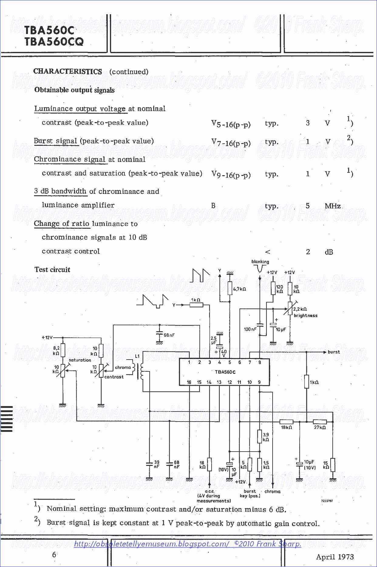


The TBA560C is a monolithic integrated circuit used in the decoding system of colour television receivers. The circuit consists of a luminance and a chrominance amplifier. The luminance amplifier input is matched to the luminance delay line and performs the following functions: d. c. contrast control ':' brightness control ':' black level clamping ':' blanking. The chrominance amplifier comprises: gain -controlled amplifier ':' chrominance gain control tracked with contrast control ':' separate d. c. saturation control ':' PAL delay line driver ':' burst gate ~, colour killer.
Balanced chroma signal input (in conjunction with pin 15)
This is derived from the chroma signal bandpass filter, designed to provide the push -pull input. An input signal amplitude of at least 4 mV peak-to -peak is required on pins 1 and 15. Both pins require a d. c. potential of approximately +3, 0 V. This is derived as a common -mode signal from a network connected to pin 7 (burst out- put). In this way d. c. feedback is provided over the burst channel to stabilise its operation.
All figures for the chrominance signals are based on a colour bar signal with 75% saturation: i.e. burst-to-chroma ratio of input signal is 1: 2. D. C. contrast control With +3, 7 Von this pin, the gain in the luminance channel is such that a 1~ 5 rnA peak-to-peak input signal to pin 3 gives a luminance output· signal amplitude on pin 5 of 3 V black-to-white. A variation of voltage on pin 2 between +6 V and +2 V gives a corresponding gain variation of +6 to > -14 dB. A similar variation in gain in the chroma channel occurs in order to provide the correct tracking between the two signals.
Luminance signal input
This terminal has a very low input impedance and acts as a current sink. The luminance signal from the delay line is fed via a series terminating resistor and must have about 1,5 rnA black-to-white amplitude. Charge storage capacitor for black level clamp (5,0 IlF)
Luminance signal output
An emitter follower provides a low impedance output signal of 3 V black-to-white amplitude at nominal contrast setting having a black level in the range 0 to +3 V. An external emitter load resistor is required. not less than 1 kQ. Black level shift at contrast control is max. ± 20 mV if the luminance input current during black level is about 0,75 rnA. When this current has a different value a larger black level shift has to be taken into account. If the input current during black level differs 1. rnA from the nominal value of 0,75 rnA, the black level shift will be about 100 mV over the complete contrast control range. For smaller differences of the input current the black level shift will be correspondingly smaller. Black level shift with video signal content occurs only when the input signal is a. c. coupled. The value depends on the drive current amplitude and can be calculated from
TBA520. PAL synchronous demodulator.
The TBA520 is an integrated colour demodulator circuit for colour television receivers, incorporating two active synchronous demodulators for R- Y and B- Y chrominance signals, a matrix (producing the G- Y colour difference signal), PAL phase switch and flip-flop. It is suitable for d. c. -coupled drive to the picture tube when associated with the matrix integrated circuit (TBA530) and RGB output stages.
The function is quoted against the corresponding pin number (see also page 5).
1. Identification bias The input current required to stop the flip"-flop, "ldent on": Ion 2: 80 fJA. For "ldent off": Voff = -5 to -to. 4 V.
2. R - Y subcarrier reference input An 1 Vpeak to peak signal is requiredviaad. c. blockingcapacitor. Under no cir- cumstances should this signal be less than 0.5 V peak to peak. The input r~sistance at this pin lies between 670 Q and 1250 Q. (Y2-16 = 0.8 to 1.5 mQ-l)
3. P. A. L. square wave output The amplitude is 2: 3 V peak to peak from an emitter follower.
4. R-Y signal output (G-Y at pin 5 and B-Y at pin 7) No external d. c. load needed except that direct connection must be made via the low pass filter to the R. G. B. matrix TBA530. The signals produced are in the following ratios: VB-Y = 1. 3 VR-Y ± 10% (a) VG-Y= 0.76 VR-Y ± 10% (b) VG-Y= 0.26 VR-Y ± 15 % Condition (a) refers to (B-Y) + (R-Y) addition in the G-Y matrix. Condition (b) refers to the phase reversed (R - Y) input signal where (G -Y) is obtained by subtraction. The d.c. levels should each be adjusted, starting with the (B-Y), to +7.5 V at nominal supply voltage.
The maximum peak to peak voltages for the condition m o. 7 (m = ratio of minimum to maximum differential gains) are:
VR-Y(p-p) 2. 3.2 V
VG-Y(p-p):::' 1. 8 V
VB-Y(p-p) :::; 4.0 V
The output impedance for each signal is 2. 7 kQ. The drifts in d. c. levels of the colour difference output signals for a change in ambient temperature of 40 °c (after equilibrium is reached from switch -on) are typically:
Absolute shift -50 to +50 mV
VR-Y relative to VB-Y -20 to +20 mV
VG-Y relative to VB-Y -20 to +20 mV
VR-Y relative to VG-Y -20 to +20 mV.


Vision IF IC:The TDA440 vision i.f. strip i.c. is housed in a 16 -pin plastic pack
with a copper frame. There is a three -stage vision i.f. amplifier with
a.g.c. applied over two stages, synchronous vision demodulator, gated
a.g.c. system and a pair of video signal pre amplifiers which provide
either positive- or negative - going outputs. Fig. 2 shows the i.c. in
block diagram form. It is possible to design a very compact i.f. strip
using this device and very ex act
performance is claimed. Note that apart from the tuned circuits which
shape the passband at the input the only tuned circuit is the 39.5MHz
carrier tank circuit in the limiter/demodulator section. The only other
adjustments are the tuner a.g.c. delay potentiometer and a potentiometer
(the one shown on the right-hand side) which sets the white level at
the demodulator. This of course gives ease of setting up, a help to
setmaker and service department alike. For a sensitivity of 200/4V the
output is 3.3V peak - to -peak, giving an overall gain in the region of
82 to 85dB. The a.g.c. range is 55dB, a further 30 to 40dB being
provided at the tuner. The tuner a.g.c. output is intended for use with a
pnp transistor or pin diode tuner unit: an external inverter stage is
required with the npn transistor tuner units generally used. discrete
component video output stage; in a colour In a monochrome set the output
would be fed to a design the output is fed to the chrominance section
of the TDA1150 and, via the luminance delay line, to the luminance
channel in the TDA1150. Also of course in both cases to the sync
separator which in this series of i.c.s is contained in the TDA1180.
act
performance is claimed. Note that apart from the tuned circuits which
shape the passband at the input the only tuned circuit is the 39.5MHz
carrier tank circuit in the limiter/demodulator section. The only other
adjustments are the tuner a.g.c. delay potentiometer and a potentiometer
(the one shown on the right-hand side) which sets the white level at
the demodulator. This of course gives ease of setting up, a help to
setmaker and service department alike. For a sensitivity of 200/4V the
output is 3.3V peak - to -peak, giving an overall gain in the region of
82 to 85dB. The a.g.c. range is 55dB, a further 30 to 40dB being
provided at the tuner. The tuner a.g.c. output is intended for use with a
pnp transistor or pin diode tuner unit: an external inverter stage is
required with the npn transistor tuner units generally used. discrete
component video output stage; in a colour In a monochrome set the output
would be fed to a design the output is fed to the chrominance section
of the TDA1150 and, via the luminance delay line, to the luminance
channel in the TDA1150. Also of course in both cases to the sync
separator which in this series of i.c.s is contained in the TDA1180.


 BU208(A)
Silicon NPNnpn transistors,pnp transistors,transistors
Category: NPN Transistor, Transistor
MHz: <1 MHz
Amps: 5A
Volts: 1500V
HIGH VOLTAGE CAPABILITY
JEDEC TO-3 METAL CASE.
DESCRIPTION
The BU208A, BU508A and BU508AFI are
manufactured using Multiepitaxial Mesa
technology for cost-effective high performance
and use a Hollow Emitter structure to enhance
switching speeds.
APPLICATIONS:
* HORIZONTAL DEFLECTION FOR COLOUR TV With 110° or even 90° degree of deflection angle.
ABSOLUTE MAXIMUM RATINGS
Symbol Parameter Value Unit
VCES Collector-Emit ter Voltage (VBE = 0) 1500 V
VCEO Collector-Emit ter Voltage (IB = 0) 700 V
VEBO Emitter-Base Voltage (IC = 0) 10 V
IC Collector Current 8 A
ICM Collector Peak Current (tp < 5 ms) 15 A
TO - 3 TO - 218 ISOWATT218
Ptot Total Dissipation at Tc = 25 oC 150 125 50 W
Tstg Storage Temperature -65 to 175 -65 to 150 -65 to 150 oC
Tj Max. Operating Junction Temperature 175 150 150 °C
There is known from German Auslegeschrift No. 2403331 a line output stage in which the deflection coil forms part of a parallel resonant circuit connected in parallel with one of two diodes which form a series combination connected in reverse parallel with a transistor constituting a controllable switch.
TBA800 Monolithic integrated AF power amplifier max. 5 W @ 16 Ω.


The TBA800 is a monolithic audio power amplifier. The external
cooling tabs enable 2.5 watts output power to be achieved without
external heat sink and 5 watts output power using a small area of the pc
board copper as a heat sink. It is ideally suited as an audio amplifier
in solid state television receivers and other class B audio amplifier
applications.
No comments:
Post a Comment
The most important thing to remember about the Comment Rules is this:
The determination of whether any comment is in compliance is at the sole discretion of this blog’s owner.
Comments on this blog may be blocked or deleted at any time.
Fair people are getting fair reply. Spam and useless crap and filthy comments / scrapers / observations goes all directly to My Private HELL without even appearing in public !!!
The fact that a comment is permitted in no way constitutes an endorsement of any view expressed, fact alleged, or link provided in that comment by the administrator of this site.
This means that there may be a delay between the submission and the eventual appearance of your comment.
Requiring blog comments to obey well-defined rules does not infringe on the free speech of commenters.
Resisting the tide of post-modernity may be difficult, but I will attempt it anyway.
Your choice.........Live or DIE.
That indeed is where your liberty lies.
Note: Only a member of this blog may post a comment.