


FARB BAUSTEIN 29301-024.01 (LUMINANCE+CHROMINANCE WITH TDA2510+TDA2521/2)
NF BAUSTEIN 29301-004.21 (AUDIO STAGE) ( TDA4290 + TDA2030)
ZF BAUSTEIN 29301-002.56 (IF MODUL WITH TDA2840 + TBA120T + TBA1440G + SN29767NA)
TP EMPFAENGER 29301-047.21 (IR REMOTE RECEIVER WITH SM568 + SM559B)
VERTIKAL BAUSTEIN 29301-009.03 (FRAME OSC UNIT) (BSV57B)
O/W DIODEN BAUSTEIN 29301-041.01
UHR BAUSTEIN (CLOCK TIME) 29301-043.21 TMS3741NL + TMS3891
HORIZONTAL BAUSTEIN 29301-008.05 (SYNCH + LINE OSC WITH TDA2591)
REGEL BAUSTEIN 29301-035.04 (LINE DEFL. REGULATION UNIT WITH SN74LS221N)

TBA
 120T (Siemens) SIF
LINE DEFL. REGULATION UNIT WITH SN74LS221N /REGEL BAUSTEIN 29301-035.04
The ’221 and ’LS221 devices are dual
multivibrators with performance characteristics
virtually identical to those of the ’121 devices.
Each multivibrator features a negative-transitiontriggered
input and a positive-transition-triggered
input, either of which can be used as an inhibit
input.

Pulse triggering occurs at a particular voltage level and is not directly related to the transition time of the input
pulse. Schmitt-trigger input circuitry (TTL hysteresis) for B input allows jitter-free triggering from inputs with
transition at rates as slow as 1 V/s, providing the circuit with excellent noise immunity, typically of 1.2 V. A high
immunity to VCC noise, typically of 1.5 V, also is provided by internal latching circuitry.
Once fired, the outputs are independent of further transitions of the A and B inputs and are a function of the timing
components, or the output pulses can be terminated by the overriding clear. Input pulses can be of any duration
relative to the output pulse. Output pulse length can be varied from 35 ns to the maximum by choosing
appropriate timing components. With Rext = 2 kΩ and Cext = 0, an output pulse typically of 30 ns is achieved
that can be used as a dc-triggered reset signal. Output rise and fall times are TTL compatible and independent
of pulse length. Typical triggering and clearing sequences are shown as a part of the switching characteristics
waveforms.
Pulse-width stability is achieved through internal compensation and is virtually independent of VCC and
temperature. In most applications, pulse stability is limited only by the accuracy of external timing components.
Jitter-free operation is maintained over the full temperature and VCC ranges for more than six decades of timing
cap
acitance (10 pF to 10 µF) and more than one decade of timing resistance (2 kΩ to 30 kΩ for the SN54221,2 kΩ to 40 kΩ for the SN74221, 2 kΩ to 70 kΩ for the SN54LS221, and 2 kΩ to 100 kΩ for the SN74LS221).
Throughout these ranges, pulse width is defined by the relationship: tw(out) = CextRext In2 ≈ 0.7 CextRext. In
circuits where pulse cutoff is not critical, timing capacitance up to 1000 µF and timing resistance as low as 1.4 kΩ
can be used. Also, the range of jitter-free output pulse widths is extended if VCC is held to 5 V and free-air
temperature is 25°C. Duty cycles as high as 90% are achieved when using maximum recommended RT. Higher
duty cycles are available if a certain amount of pulse-width jitter is allowed.
The variance in output pulse width from device to device typically is less than ±0.5% for given external timing
components. An example of this distribution for the ’221 is shown in Figure 3. Variations in output pulse width
versus supply voltage and temperature for the ’221 are shown in Figures 4 and 5, respectively.
Pin assignments for these devices are identical to those of the SN54123/SN74123 or SN54LS123/SN74LS123
so that the ’221 or ’LS221 devices can be substituted for those products in systems not using the retrigger by
merely changing the value of Rext and/or Cext; however, the polarity of the capacitor must be changed.
FUNCTION TABLE
(each monostable multivibrator)
INPUTS OUTPUTS
CLR A B Q Q
L X X L H
X H X L H
X X L L H
H L ↑ † †
H ↓ H † †
↑‡ L H † †
† Pulsed-output patterns are tested during
AC switching at 25°C with Rext = 2 kΩ, and
Cext = 80 pF.
‡ This condition is true only if the output of
the latch formed by the two NAND gates
has been conditioned to the logic 1 state
prior to CLR going high. This latch is
conditioned by taking either A high or
B low while CLR is inactive (high).
absolute maximum ratings over operating free-air temperature range (unless otherwise noted)†
Supply voltage range, VCC 7 V . . . . . . . . . . . . . . . . . . . . . . . . . . . . . . . . . . . . . . . . . . . . . . . . . . . . . . . . . . . . . . . . . . .
Input voltage range, VI (see Note 1): ’LS221 7 V . . . . . . . . . . . . . . . . . . . . . . . . . . . . . . . . . . . . . . . . . . . . . . . . . . .
’221 5.5 V . . . . . . . . . . . . . . . . . . . . . . . . . . . . . . . . . . . . . . . . . . . . . . . . . . . .
Package thermal impedance, θJA (see Note 2): D package 73°C/W . . . . . . . . . . . . . . . . . . . . . . . . . . . . . . . . . . .
DB package 82°C/W . . . . . . . . . . . . . . . . . . . . . . . . . . . . . . . . .
N package 67°C/W . . . . . . . . . . . . . . . . . . . . . . . . . . . . . . . . . . .
NS package 64°C/W . . . . . . . . . . . . . . . . . . . . . . . . . . . . . . . . .
Storage temperature range, Tstg −65°C to 150°C.
TDA2591 SYNCHRO AND HORIZONTAL DEFLECTION CONTROL FOR COLOR TV SET
DESCRIPTION
The TDA2591 is a circuit intended for the horizontal
deflection of color TVsets, supplied with transistors
or SCR’S.
The TDA2591 and TDA2593 are integrated line
oscillator ‘_circuits for colour television receivers using
thyristor or transistor line deflection output stages.
The _circuits incorporate a line oscillator ‘which is
based on the threshold switching principle, a line de-
flection output stage capable of direct drive of thyristor
deflection circuits, phase comparison between the
oscillator voltage and both the sync pulse and line
flyback pulse. Also included on the chip is a switch for
changing the filter characteristic and the gate circuit
when used for VCR.
The TDA2593 generates a sandcastle pulse (at pin
7) suitable for use with the TDA.2532.
.LINE OSCILLATOR(two levels switching)
.PHASE COMPARISON BETWEEN SYNCHRO-
PULSE AND OSCILLATOR VOLTAGE Ø 1, ENABLED BY AN INTERNAL PULSE,
(better parasitic immunity)
PHASE COMPARISON BETWEEN THE FLYBACK
PULSES AND THE OSCILLATOR VOLTAGE Ø2
.COINCIDENCE DETECTOR PROVIDING A LARGE HOLD-IN-RANGE.
.FILTER CHARACTERISTICS AND GATE SWITCHING FOR VIDEO RECORDER APPLICATION.
.NOISE GATED SYNCHRO SEPARATOR
.FRAME PULSE SEPARATOR .BLANKING AND SAND CASTLE OUTPUT PULSES
.HORIZONTAL POWER STAGE PHASE LAGGING CIRCUIT
.SWITCHING OF CONTROL OUTPUT PULSE WIDTH
.SEPARATED SUPPLY VOLTAGE OUTPUT STAGE ALLOWING DIRECT DRIVE OF SCR’S CIRCUIT
.SECURITY CIRCUIT MAKES THE OUTPUT PULSE SUPPRESSED WHEN LOW SUPPLY
VOLTAGE.
TDA2030,14W Hi-Fi AUDIO AMPLIFIER
DESCRIPTION
The TDA2030 is a monolithic integrated circuit in
Pentawatt[ package, intended for use as a low
frequency class AB amplifier. Typically it provides
14W output power (d = 0.5%) at 14V/4W; at ± 14V
the guaranteed output power is 12W on a 4W load
and 8Won a 8W (DIN45500).
TheTDA2030provideshigh outputcurrentand has
very low harmonic and cross-over distortion.
Further the device incorporates an original (and
patented) short circuit protection system comprising
an arrangement for automatically limiting the
dissipated power so as to keep the working point
of the output transistors within their safe operating
area. A conventional thermal shut-down system is
also included.
SHORT CIRCUIT PROTECTION
The TDA2030 has an original circuit which limits the
current of the output transistors. Fig. 18 showsthat
the maximum output current is a function of the
collector emitter voltage; hence the output transistors
work within their safe operating area (Fig. 2).
This function can thereforebe considered as being
peak power limiting rather than simple current limiting.
It reduces the possibility that the device gets damaged
during an accidental short circuit from AC
output to ground.
TDA2521 synchronous demodulator for PAL
GENERAL DESCRIPTION
The TDA2521 is a monolithic integrated circuit designed as a synchronous demodulator for PAL color television receivers. It includes an 8.8 MHz oscillator and divider, to generate two 4.4 MHz reference signals, and provides color difference output.

The TDA2521 is intended to interface directly with the TDA251O with a minimum of external components and is constructed on a single silicon chip using the Fairchild Planar
epitaxial process.
ABSOLUTE MAXIMUM RATINGS
Supply Voltage 14 V
Internal Power Dissipation 600 mW ORDER INFQRMATIQN
Operating Temperature Range —2O°C to +6O°C TYPE PART NO.
Storage Temperature Range —55°C to +125°C 2521 TDA2521
Pin Temperature iSo|dering 10 si 260°C
Planar is a patented Fairchild process

TDA2510 CHROMINANCE COMBINATION
GENERAL DESCRIPTION —

The TDA2510 is a monolithic integrated circuit designed for the function of a color television receiver. It Is designed to Interface directly with the TDA2521, using a minimum number of external components.
TDA251O is constructed on a single silicon chip using the Fairchild Planar‘ epitaxial process.
ABSOLUTE MAXIMUM RATINGS
supply Voltage 15 V
Collector voltage of chroma output transistor (pin 7) 20 V
(PD I 100 mW max)
Collector current of chroma output transistor (pin 7) 20 mA
Collector current of color killer output transistor (pin 11) 10 mA
Power dissipation 500 mW
Operating temperature range —25°C 10 +6O°
Storage temperature range *55°C to +12!-3°C
Tone Control IC TDA 4290-2
TDA 4290-2 S
Bipolar IC
Tone control lC for the DC voltage control of volume, treble, and bass. The volume characteristic
can be changed from linear to physiological.
For mono application we recommend the TDA 4290-2, while the TDA 4290-2 S is especially
suitable for stereo application.
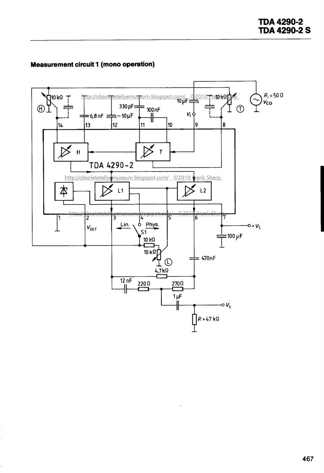
O Few external components
Q High signal-to-noise ratio
O Low total harmonic distortion
O Complies with the IEC 268-3 standards
Maximum ratings
Supply voltage VS 18 V
Control inputs V5, V8, V14 O to Vs V
Input signal V8,,“ 3 V
Load current I2 10 mA
Junction temperature 7] 150 °C
Storage temperature range Tm -40 to 125 “C
Thermal resistance (system-air) Rm SA 90 K/W
Operating range
Supply voltage VS 10.5 to 18 V
Volume control V5 0 to 0.51 x V2 V
Frequency (—1 dB) fi 20 to 20,000 Hz
Ambient temperature TA O to 70 °C
GRUNDIG SUPER COLOR Einschub W8272 IT CHASSIS 29301-114.63 Automatic peak beam current limiter:
In a video signal processing system, apparatus for limiting excessive peak and average beam currents demanded by a kinescope in response to image representative video signals. A control signal derived by a sensing circuit in response to excessive beam current is applied to the kinescope in a manner to limit excessive beam currents above a threshold level. The sensing circuit includes a capacitor arranged with a conductive diode to form an average responding filter such that the sensing circuit derives a control voltage representative of excessive average beam current in a first beam current limiting mode. In a second beam limiting mode, when beam current exceeds a predetermined level, the diode is rendered nonconductive and the capacitor is decoupled for average detection purposes. In this mode, the control signal is free to vary in accordance with rapid variations in peak beam current.  1. In a video signal processing system including a kinescope for reproducing an image in response to video signals, apparatus for limiting excessive kinescope current conduction comprising:
 means for deriving a control signal indicative of variations in the magnitude of kinescope current above a selected threshold level; and
means for utilizing said control signal to limit kinescope current in accordance with the magnitude of said control signal; and wherein
said control signal deriving means includes filter means subject to alternative operation in a first state and a second state; said filter means, when in said first state, exhibiting a restricted pass band such that said control signal is indicative of only relatively long term variations in the magnitude of said kinescope current; said filter means, when in said second state, exhibiting a pass band significantly wider than said restricted pass band such that said control signal additionally follows relatively short term variations in said kinetic current; and said filter means being subject to switching from said first state to said second state when said kinescope current exceeds a predetermined level.
2. Apparatus according to claim 1, wherein said signal deriving means additionally comprises a controlled conduction device exhibiting first and second conductive states in the presence of excess kinescope current exhibiting said relatively long and short term variations, respectively. 3. Apparatus according to claim 2, wherein:
said control signal is developed across the series combination of a filter capacitor and said controlled conduction device, said controlled conduction device exhibiting a high impedance in said second conductive state.
4. Apparatus according to claim 2 and further comprising a source of supply current representative of the magnitude of current conducted by said kinescope, wherein
said signal deriving means is coupled to said current source for sensing the level of said supply current to thereby derive said control signal when said supply current exceeds the threshold level; and
a source of reference current is coupled to said controlled device for maintaining said device in said first conductive state, said device exhibiting said second conductive state when said supply current exhibits said relatively short term variations and exceeds a predetermined level.
5. Apparatus according to claim 4, wherein
the magnitude of said reference current exceeds said threshold level;
said controlled device exhibits said first conductive state when the magnitude of supply current exhibits said long term variations and exceeds the threshold level; and
said controlled device exhibits said second conductive state when the magnitude of supply current exhibits said short term variations and exceeds the magnitude of said reference current by a predetermined amount.
6. Apparatus according to claim 4 and further comprising high voltage supply means for providing an operating supply for said kinescope; and wherein
said current source is coupled to an input of said high voltage means and said supply current corresponds to the current drawn by said kinescope from said high voltage means in accordance with the level of kinescope current conduction.
7. Apparatus according to claim 6, wherein:
said current source provides a given current with a magnitude corresponding to said threshold level, said last-named current being supplied to said high voltage means as said supply current in accordance with the level of kinescope current conduction; and
said controlled device exhibits said second conductive state when said supply current exceeds the sum of said reference current and said given current.
8. Apparatus according to claim 7, wherein: the level of said reference current is substantially equal to or less than the level of said given current. 9. Apparatus according to claim 4, wherein:
said controlled device comprises a semiconductor PN junction device coupled between a first point and a point of reference potential, said semiconductor being rendered conductive in response to said reference current; and
said filter means comprises a capacitor coupled to said first point and to said current source at a second point remote from said first point, for sensing said supply current.
10. Apparatus according to claim 9, wherein:
said semiconductor device is rendered non-conductive and said capacitor is decoupled from said point of reference potential when supply current exhibiting said relatively short term variations exceeds the magnitude of the said reference current by a predetermined amount.
11. Apparatus according to claim 1 and further comprising:
a channel for processing said video signals;
means for coupling video signals processed by said channel to said kinescope; and wherein
said control signal is coupled to said channel for translating the video signal in a direction to limit excessive kinescope current conduction in accordance with the magnitude of said control signal.
12. Apparatus according to claim 11, wherein:
said control signal is utilized to vary the D.C. level of signals processed by said channel in a direction to limit excessive kinescope current conduction.
13. In a television signal processing system including a kinescope for reproducing an image in response to processed television signals, apparatus for limiting excessive kinescope beam currents exhibiting relatively long term and short term variations, comprising:
a source of supply current representative of the magnitude of beam current demanded by said kinescope;
means including a filter capacitor, coupled to said current source for sensing said supply current to thereby derive a control signal representative of the magnitude of excessive beam current above a given threshold level as manifested by the level of said supply current;
means for coupling said control signal to said kinescope for limiting beam current above the threshold level in accordance with the magnitude of said control signal; and wherein
said signal deriving means additionally includes:
a threshold conducting device coupled between a terminal of said capacitor remote from said current source and a point of reference potential; and
a source of reference current for biasing said device for conduction between said capacitor terminal and said point of reference potential, the level of said reference current being in predetermined relationship with said threshold current level.
14. Apparatus according to claim 13, wherein:
said control signal is utilized to vary a luminance signal component of said television signal in a direction to limit kinescope beam current conduction above the threshold level; and
said threshold device comprises a semiconductor PN junction device poled for forward current conduction from said capacitor terminal to said reference potential.
Description:
This invention relates to apparatus for automatically limiting excessive beam currents drawn by an image reproducing device in a video signal processing system such as a television receiver. In particular, the invention relates to such apparatus capable of limiting short duration peak beam currents as well as average beam currents of relatively longer duration.
Excessive peak or average beam currents can cause a television receiver to produce a degraded image. In this regard, excess beam currents can cause degradation of the performance of the receiver deflection system which is operatively associated with an image reproducing kinescope, electron beam spot defocussing, and picture blooming. High beam currents can also exceed the safe operating current capability of the kinescope, possibly damaging the kinescope and associated circuit components which may be sensitive to high beam current levels.
Various automatic beam current limiter circuits responsive to average beam current levels are known. These circuits typically respond to excessive beam current levels occurring at a rate not exceeding the vertical image scanning rate of the kinescope. The average responding circuits essentially ignore peak increases in beam current levels occurring only for a few horizontal image lines of a vertical scanning interval, for example. Because of the inherent insensitivity of average responding circuits to transient or peak increases in beam current of less than average duration (e.g., less than a vertical image scanning period), a special problem exists for video signal processing systems wherein it is desired to limit such peak currents for a variety of reasons. Excessive peak beam current levels can be attributable to the information content of a received image-representative video signal, such as a signal representative of black-to-white image transitions occurring in one or more succeeding vertical image scanning intervals. Excessive peak beam currents can also occur as a result of transients produced when switching from one channel of the receiver to another. In any case, excessive peak beam current levels can adversely affect receiver circuits (e.g., deflection circuits) which may be sensitive to high levels of peak beam current, even if the maximum allowable average beam current level has not been exceeded.
 Systems which provide for limiting both average and peak beam currents are known. For example, U.S. Pat. No. 3,980,822 (Suzuki et al.) discloses an arrangement wherein excess average beam currents are sensed and limited by means including a first limiter circuit with a first time constant. Peak or transient beam currents are sensed and limited by a second limiter circuit, distinct from the first circuit, exhibiting a short time constant relative to the first time constant. U.S. Pat. No. 4,017,681 (Smeulers et al.) also discloses an arrangement including a circuit for detecting excess peak beam currents, and a separate circuit for detecting excess average beam currents.
An analogous arrangement is disclosed in U.S. Pat. No. 3,914,545 (Engel). This patent describes a system wherein a derived control signal representative of the average level of a luminance signal varies the gain of a luminance signal amplifier inversely with changes in the average level. The control signal is modified by a peak limiter circuit whenever the instantaneous luminance signal exceeds a threshold level. The control signal is further modified by a signal from a beam current limiter network responsive to high levels of average beam current.
Because of the nature of a peak or transient excess beam current condition, a peak beam current limiter should exhibit a rapid response in order to provide appropriate compensation. It is also desirable in many instances for an automatic beam current limiter to be capable of limiting both excessive peak and average beam currents. Particularly in this instance, complex, uneconomical circuit arrangements should be avoided whenever possible.
Apparatus according to the present invention is included in a video signal processing system having a kinescope for reproducing an image in response to video signals, for limiting excessive kinescope current conduction. The apparatus includes a sensing circuit for deriving a control signal indicative of variations in the magnitude of kinescope current above a selected threshold level. The control signal is utilized to limit kinescope current in accordance with the magnitude of the control signal. The sensing circuit includes a filter network subject to alternative operation in first and second states. When in the first operating state, the filter exhibits a restricted pass band such that the control signal is indicative of only relatively long term variations in the magnitude of the kinescope current. When in the second operating state, the filter exhibits a significantly wider pass band such that the control signal additionally follows relatively short term variations in kinescope current. The filter network is subject to switching from the first to the second state when the kinescope current exceeds a predetermined level.
The single FIGURE of the drawing shows, partially in block diagram form and partially in schematic circuit diagram form, a general arrangement of a color television receiver employing apparatus constructed in accordance with the present invention.
The drawing depicts a color television receiver including a video signal processing unit 12 for receiving radio frequency signals from an antenna 10 and for translating these signals through intermediate frequency amplifying and detecting stages (not shown) to provide a composite video signal. The composite video signal contains luminance, chrominance, sound and synchronizing components.
A sync separator 15 serves to separate the synchronizing (sync) component from the composite video signal to provide periodic line sync pulses. These pulses are further processed by sync processing and deflection circuits 16 to provide horizontal flyback signals, and horizontal and vertical blanking and deflection signals as known.
A frequency selection unit 21 (e.g., a bandpass filter) selectively couples the chrominance component of the composite video signal to chrominance signal processing unit 24 (e.g., including amplifier and demodulator stages) to derive R-Y, B-Y and G-Y color difference signals. These signals are applied as inputs to a kinescope driver stage 60.
The luminance component of the composite video signal is amplified and otherwise processed by a luminance signal processing unit 35 in a luminance channel of the receiver. Luminance processing unit 35 includes a luminance signal clamping circuit for providing a clamped luminance output signal Y, as disclosed in a copending U.S. patent application Ser. No. 819,935 of R. P. Parker, now U.S. Pat. No. 4,110,787 entitled "Combined Blanking Level And Kinescope Bias Clamp For A Television Signal Processing System", assigned to the same assignee as the present invention. The periodic operation of the clamping circuit is controlled in response to periodic blanking pulses supplied during each image retrace blanking interval by a source of blanking pulses 54. Periodic auxiliary blanking pulses of predetermined magnitude supplied by an auxiliary blanking unit 45 are added to the luminance signal prior to clamping during each blanking interval. This and other aspects of unit 35 are described in greater detail in the last mentioned U.S. patent application.
The clamped luminance signal Y is supplied to an input of kinescope driver 60, where the luminance signal is combined with the color difference signals from unit 24 to form R, B and G color signals. These signals are then coupled to signal inputs (e.g., cathode electrodes) of a kinescope 66 for reproducing a color image.
High operating voltages for focus (not shown) and ultor electrodes of kinescope 66 are provided by a high voltage supply 68 (e.g., voltage tripler) in response to positive, periodic horizontal flyback pulses occurring during horizontal retrace scanning intervals. A current supply including a source of positive direct voltage (+27 volts) and a current determining resistor 72 provides a current I S and is c oupled to a D.C. input of high voltage unit 68 via a resistor 73. Current flowing in resistor 72 includes a component I R representative of the beam current (i.e., ultor current) demand of the kinescope in response to the luminance and chrominance signals. This current flows into the D.C. input of high voltage unit 68 and is sometimes referred to as a "resupply" current (i.e., a current via the high voltage unit to recharge or resupply the ultor electrode voltage of the kinescope when depleted as a result of beam current conduction). The described current supply is typically associated with the high voltage supply in a television receiver for purposes of providing the resupply current. The resupply current typically consists of current pulses recurring at the horizontal line scanning rate. Some A.C. filtering of horizontal rate voltages which these current pulses tend to produce at the D.C. input terminal of high voltage unit 68 is provided by a filter capacitor 74.
Excessive levels of peak and average beam currents are sensed by a circuit 70. Sensing network 70 is operatively associated with the supply current source including resistor 72, and comprises a large value, average responding filter capacitor 75 and a normally conductive clamp diode 78. Network 70 also includes a normally conductive diode 77 for conductively coupling the negative plate of filter capacitor 75 to a point of reference potential (ground) when beam current demand does not exceed a predetermined level under normal operating conditions of the receiver, and also when a condition of excessive average beam current demand exists, as will be discussed. Diode 77 is forward biased into conduction by a reference current I B of predetermined value, as supplied by a current source including a resistor 76 and a source of positive direct voltage (+27 volts).
A voltage representative of the level of resupply current (i.e., ultor current) is developed on the positive terminal of capacitor 75 when the resupply current exceeds a predetermined threshold level indicating the presence of excessive peak or average beam current demand, as will be explained. This voltage is supplied to an input of a gated automatic beam limiter (ABL) control network 90, which can be of the type disclosed in a copending, concurrently filed U.S. patent application of R. P. Parker, entitled "Gated Automatic Beam Current Limiter In A Video Signal Processing System", and assigned to the present assignee. Unit 90 then develops an output control signal in accordance with the magnitude of the excessive peak or average beam currents. This control signal is applied to luminance processor 35 in such a manner as to translate the luminance signal in a direction to limit excess beam currents.
In accordance with this invention, the otherwise average responding operation of sensing circuit 70 is modified in the presence of high levels of peak or momentary beam current demand, as manifested by resupply current I R . This is accomplished by the coaction of filter capacitor 75 with diode 77 and reference bias current I B .
During normal operating conditions, diode 78 clamps the voltage at the positive terminal of capacitor 75 to +11 volts plus the voltage drop across diode 78 (approximately 0.6 volts), or +11.6 volts. A portion of current I S flows through clamp diode 78 when conducting. The control signal output from ABL network 90 is inhibited during this time, whereby the luminance signal is processed in normal fashion by unit 35.
The value of resistor 72 and the voltage drop thereacross (15.4 volts) determine a normal level of current I S (0.7 milliamperes), which corresponds to a first threshold current level of beam limiter operation. This current divides between diode 78 when conducting and the D.C. input of high voltage source 68 in accordance with the beam current demand of kinescope 66 as manifested by the level of resupply current I R .
Sensing circuit 70 exhibits dual mode operation for sensing both excessive average and peak beam current demand. Diode 77 and reference current I B are specifically employed for this purpose. The threshold level at which peak beam currents are sensed and limited is determined by the magnitude of current I B (approximately 2.25 milliamperes).
When the average resupply current exceeds the first threshold level determined by current I S , current drive for clamp diode 78 is depleted and diode 78 ceases conducting. Since the positive terminal of capacitor 75 is no longer clamped by diode 78, the voltage at this terminal decreases to a less positive level at a rate determined by the amount by which the first threshold current level is exceeded. The ABL control network 90 responds to this less positive voltage by providing a corresponding output control signal which serves, for example, to translate the D.C. level of the luminance signal in a direction to cause kinescope 68 to conduct proportionally less average beam current. Under this condition, diode 77 remains conductive and current I B flows to ground through diode 77, thereby preserving the role of capacitor 75 as a low pass, average responding filter.
The role of capacitor 75 as an average responding filter is altered when kinescope 66 momentarily demands high peak levels of resupply current. Specifically, as in the case of excessive average current demand, a sudden large increase in resupply current I R in response to beam current demand causes the positive terminal of capacitor 75 to become less positive when the first threshold current level is exceeded.
Diode 77 ceases conducting since the forward bias current for diode 77 otherwise provided by current I B now flows through capacitor 75 instead of through diode 77 to ground, in accordance with the rate of change of capacitor 75 voltage and the magnitude of the peak resupply current demand. This effect is produced since the current through a capacitor (e.g., capacitor 75) is determined by the product of the value of the capacitor and the rate of change of voltage across the capacitor. Thus for a given value of capacitance, the capacitor current increases as the rate of change of capacitor voltage increases. In this instance, the rapid rate of change of the voltage across capacitor 75 is produced in response to the sudden increase in peak resupply current. This rapid rate of voltage change is essentially unaffected by the small value of horizontal rate filter capacitor 74.
With capacitor 75 being deco upled in the presence of a rapid increase in peak resupply current demand as described, the current I B then flowing through capacitor 75 thereafter flows primarily in the resupply current path to the resupply current input of high voltage supply 68. The beam current representative control voltage appearing at the positive terminal of capacitor 75 decreases rapidly in accordance with any further rapid increase in the level of resupply current I R , since capacitor 75 no longer acts as a low pass, average responding filter during this condition. The described action permits the beam limiter control circuitry to respond quickly (i.e., track closely) and limit rapid or momentary increases in beam current demand, greater than the vertical scanning rate, in accordance with the magnitude of the control signal appearing at the positive terminal of capacitor 75.
It is noted that the level at which peak beam current limiting commences can be adjusted to suit the requirements of a particular system by tailoring the value of reference bias current I B . Specifically, peak beam current limiting can be activated sooner by reducing the value of reference current I B . When this rapidly increasing resupply current exhibits a magnitude equal to the sum of reference current I B and supply current I S , the current in capacitor 75 equals current I B . Therefore, diode 77 ceases conducting and capacitor 75 is decoupled from ground. The sum of currents flowing through resistor 76 and resistor 72 then increases in accordance with the amount by which current I R increases above the sum of currents I S and I B .
While the invention has been described in terms of a preferred embodiment, it should be recognized that various modifications can be made by persons skilled in the art without departing from the scope of the invention. Component values and other examples of operating parameters have been mentioned as an aid to understanding the invention and are not intended to be limiting.
Excessive peak or average beam currents can cause a television receiver to produce a degraded image. In this regard, excess beam currents can cause degradation of the performance of the receiver deflection system which is operatively associated with an image reproducing kinescope, electron beam spot defocussing, and picture blooming. High beam currents can also exceed the safe operating current capability of the kinescope, possibly damaging the kinescope and associated circuit components which may be sensitive to high beam current levels.
Various automatic beam current limiter circuits responsive to average beam current levels are known. These circuits typically respond to excessive beam current levels occurring at a rate not exceeding the vertical image scanning rate of the kinescope. The average responding circuits essentially ignore peak increases in beam current levels occurring only for a few horizontal image lines of a vertical scanning interval, for example. Because of the inherent insensitivity of average responding circuits to transient or peak increases in beam current of less than average duration (e.g., less than a vertical image scanning period), a special problem exists for video signal processing systems wherein it is desired to limit such peak currents for a variety of reasons. Excessive peak beam current levels can be attributable to the information content of a received image-representative video signal, such as a signal representative of black-to-white image transitions occurring in one or more succeeding vertical image scanning intervals. Excessive peak beam currents can also occur as a result of transients produced when switching from one channel of the receiver to another. In any case, excessive peak beam current levels can adversely affect receiver circuits (e.g., deflection circuits) which may be sensitive to high levels of peak beam current, even if the maximum allowable average beam current level has not been exceeded.
Systems which provide for limiting both average and peak beam currents are known. For example, U.S. Pat. No. 3,980,822 (Suzuki et al.) discloses an arrangement wherein excess average beam currents are sensed and limited by means including a first limiter circuit with a first time constant. Peak or transient beam currents are sensed and limited by a second limiter circuit, distinct from the first circuit, exhibiting a short time constant relative to the first time constant. U.S. Pat. No. 4,017,681 (Smeulers et al.) also discloses an arrangement including a circuit for detecting excess peak beam currents, and a separate circuit for detecting excess average beam currents. An analogous arrangement is disclosed in U.S. Pat. No. 3,914,545 (Engel). This patent describes a system wherein a derived control signal representative of the average level of a luminance signal varies the gain of a luminance signal amplifier inversely with changes in the average level. The control signal is modified by a peak limiter circuit whenever the instantaneous luminance signal exceeds a threshold level. The control signal is further modified by a signal from a beam current limiter network responsive to high levels of average beam current.
Because of the nature of a peak or transient excess beam current condition, a peak beam current limiter should exhibit a rapid response in order to provide appropriate compensation. It is also desirable in many instances for an automatic beam current limiter to be capable of limiting both excessive peak and average beam currents. Particularly in this instance, complex, uneconomical circuit arrangements should be avoided whenever possible.
Apparatus according to the present invention is included in a video signal processing system having a kinescope for reproducing an image in response to video signals, for limiting excessive kinescope current conduction. The apparatus includes a sensing circuit for deriving a control signal indicative of variations in the magnitude of kinescope current above a selected threshold level. The control signal is utilized to limit kinescope current in accordance with the magnitude of the control signal. The sensing circuit includes a filter network subject to alternative operation in first and second states. When in the first operating state, the filter exhibits a restricted pass band such that the control signal is indicative of only relatively long term variations in the magnitude of the kinescope current. When in the second operating state, the filter exhibits a significantly wider pass band such that the control signal additionally follows relatively short term variations in kinescope current. The filter network is subject to switching from the first to the second state when the kinescope current exceeds a predetermined level.
The single FIGURE of the drawing shows, partially in block diagram form and partially in schematic circuit diagram form, a general arrangement of a color television receiver employing apparatus constructed in accordance with the present invention.
The d
rawing depicts a color television receiver including a video signal processing unit 12 for receiving radio frequency signals from an antenna 10 and for translating these signals through intermediate frequency amplifying and detecting stages (not shown) to provide a composite video signal. The composite video signal contains luminance, chrominance, sound and synchronizing components. A sync separator 15 serves to separate the synchronizing (sync) component from the composite video signal to provide periodic line sync pulses. These pulses are further processed by sync processing and deflection circuits 16 to provide horizontal flyback signals, and horizontal and vertical blanking and deflection signals as known.
A frequency selection unit 21 (e.g., a bandpass filter) selectively couples the chrominance component of the composite video signal to chrominance signal processing unit 24 (e.g., including amplifier and demodulator stages) to derive R-Y, B-Y and G-Y color difference signals. These signals are applied as inputs to a kinescope driver stage 60.
The luminance component of the composite video signal is amplified and otherwise processed by a luminance signal processing unit 35 in a luminance channel of the receiver. Luminance processing unit 35 includes a luminance signal clamping circuit for providing a clamped luminance output signal Y, as disclosed in a copending U.S. patent application Ser. No. 819,935 of R. P. Parker, now U.S. Pat. No. 4,110,787 entitled "Combined Blanking Level And Kinescope Bias Clamp For A Television Signal Processing System", assigned to the same assignee as the present invention. The periodic operation of the clamping circuit is controlled in response to periodic blanking pulses supplied during each image retrace blanking interval by a source of blanking pulses 54. Periodic auxiliary blanking pulses of predetermined magnitude supplied by an auxiliary blanking unit 45 are added to the luminance signal prior to clamping during each blanking interval. This and other aspects of unit 35 are described in greater detail in the last mentioned U.S. patent application.
The clamped luminance signal Y is supplied to an input of kinescope driver 60, where the luminance signal is combined with the color difference signals from unit 24 to form R, B and G color signals. These signals are then coupled to signal inputs (e.g., cathode electrodes) of a kinescope 66 for reproducing a color image.
High operating voltages for focus (not shown) and ultor electrodes of kinescope 66 are provided by a high voltage supply 68 (e.g., voltage tripler) in response to positive, periodic horizontal flyback pulses occurring during horizontal retrace scanning intervals. A current supply including a source of positive direct voltage (+27 volts) and a current determining resistor 72 provides a current I S and is c
oupled to a D.C. input of high voltage unit 68 via a resistor 73. Current flowing in resistor 72 includes a component I R representative of the beam current (i.e., ultor current) demand of the kinescope in response to the luminance and chrominance signals. This current flows into the D.C. input of high voltage unit 68 and is sometimes referred to as a "resupply" current (i.e., a current via the high voltage unit to recharge or resupply the ultor electrode voltage of the kinescope when depleted as a result of beam current conduction). The described current supply is typically associated with the high voltage supply in a television receiver for purposes of providing the resupply current. The resupply current typically consists of current pulses recurring at the horizontal line scanning rate. Some A.C. filtering of horizontal rate voltages which these current pulses tend to produce at the D.C. input terminal of high voltage unit 68 is provided by a filter capacitor 74. Excessive levels of peak and average beam currents are sensed by a circuit 70. Sensing network 70 is operatively associated with the supply current source including resistor 72, and comprises a large value, average responding filter capacitor 75 and a normally conductive clamp diode 78. Network 70 also includes a normally conductive diode 77 for conductively coupling the negative plate of filter capacitor 75 to a point of reference potential (ground) when beam current demand does not exceed a predetermined level under normal operating conditions of the receiver, and also when a condition of excessive average beam current demand exists, as will be discussed. Diode 77 is forward biased into conduction by a reference current I B of predetermined value, as supplied by a current source including a resistor 76 and a source of positive direct voltage (+27 volts).
A voltage representative of the level of resupply current (i.e., ultor current) is developed on the positive terminal of capacitor 75 when the resupply current exceeds a predetermined threshold level indicating the presence of excessive peak or average beam current demand, as will be explained. This voltage is supplied to an input of a gated automatic beam limiter (ABL) control network 90, which can be of the type disclosed in a copending, concurrently filed U.S. patent application of R. P. Parker, entitled "Gated Automatic Beam Current Limiter In A Video Signal Processing System", and assigned to the present assignee. Unit 90 then develops an output control signal in accordance with the magnitude of the excessive peak or average beam currents. This control signal is applied to luminance processor 35 in such a manner as to translate the luminance signal in a direction to limit excess beam currents.
In accordance with this invention, the otherwise average responding operation of sensing circuit 70 is modified in th
e presence of high levels of peak or momentary beam current demand, as manifested by resupply current I R . This is accomplished by the coaction of filter capacitor 75 with diode 77 and reference bias current I B . During normal operating conditions, diode 78 clamps the voltage at the positive terminal of capacitor 75 to +11 volts plus the voltage drop across diode 78 (approximately 0.6 volts), or +11.6 volts. A portion of current I S flows through clamp diode 78 when conducting. The control signal output from ABL network 90 is inhibited during this time, whereby the luminance signal is processed in normal fashion by unit 35.
The value of resistor 72 and the voltage drop thereacross (15.4 volts) determine a normal level of current I S (0.7 milliamperes), which corresponds to a first threshold current level of beam limiter operation. This current divides between diode 78 when conducting and the D.C. input of high voltage source 68 in accordance with the beam current demand of kinescope 66 as manifested by the level of resupply current I R .
Sensing circuit 70 exhibits dual mode operation for sensing both excessive average and peak beam current demand. Diode 77 and reference current I B are specifically employed for this purpose. The threshold level at which peak beam currents are sensed and limited is determined by the magnitude of current I B (approximately 2.25 milliamperes).
When the average resupply current exceeds the first threshold level determined by current I S , current drive for clamp diode 78 is depleted and diode 78 ceases conducting. Since the positive terminal of capacitor 75 is no longer clamped by diode 78, the voltage at this terminal decreases to a less positive level at a rate determined by the amount by which the first threshold current level is exceeded. The ABL control network 90 responds to this less positive voltage by providing a corresponding output control signal which serves, for example, to translate the D.C. level of the luminance signal in a direction to cause kinescope 68 to conduct proportionally less average beam current. Under this condition, diode 77 remains conductive and current I B flows to ground through diode 77, thereby preserving the role of capacitor 75 as a low pass, average responding filter.
The role of capacitor 75 as an average responding filter is altered when kinescope 66 momentarily demands high peak levels of resupply current. Specifically, as in the case of excessive average current demand, a sudden large increase in resupply current I R in response to beam current demand causes the positive terminal of capacitor 75 to become less positive when the first threshold current level is exceeded.
Diode 77 ceases conducting since the forward bias current for diode 77 otherwise provided by current I B now flows through capacitor 75 instead of through diode 77 to ground, in accordance with the rate of change of capacitor 75 voltage and the magnitude of the peak resupply current demand. This effect is produced since the current through a capacitor (e.g., capacitor 75) is determined by the product of the value of the capacitor and the rate of change of voltage across the capacitor. Thus for a given value of capacitance, the capacitor current increases as the rate of change of capacitor voltage increases. In this instance, the rapid rate of change of the voltage across capacitor 75 is produced in response to the sudden increase in peak resupply current. This rapid rate of voltage change is essentially unaffected by the small value of horizontal rate filter capacitor 74.
With capacitor 75 being deco
upled in the presence of a rapid increase in peak resupply current demand as described, the current I B then flowing through capacitor 75 thereafter flows primarily in the resupply current path to the resupply current input of high voltage supply 68. The beam current representative control voltage appearing at the positive terminal of capacitor 75 decreases rapidly in accordance with any further rapid increase in the level of resupply current I R , since capacitor 75 no longer acts as a low pass, average responding filter during this condition. The described action permits the beam limiter control circuitry to respond quickly (i.e., track closely) and limit rapid or momentary increases in beam current demand, greater than the vertical scanning rate, in accordance with the magnitude of the control signal appearing at the positive terminal of capacitor 75. It is noted that the level at which peak beam current limiting commences can be adjusted to suit the requirements of a particular system by tailoring the value of reference bias current I B . Specifically, peak beam current limiting can be activated sooner by reducing the value of reference current I B . When this rapidly increasing resupply current exhibits a magnitude equal to the sum of reference current I B and supply current I S , the current in capacitor 75 equals current I B . Therefore, diode 77 ceases conducting and capacitor 75 is decoupled from ground. The sum of currents flowing through resistor 76 and resistor 72 then increases in accordance with the amount by which current I R increases above the sum of currents I S and I B .
While the invention has been described in terms of a preferred embodiment, it should be recognized that various modifications can be made by persons skilled in the art without departing from the scope of the invention. Component values and other examples of operating parameters have been mentioned as an aid to understanding the invention and are not intended to be limiting.
I stumbled across this very interesting article by accident. Among some stuff i was given, was a small sub PCB i thought the style and construction of, looked familiar, myself being a retired TV engineer of the 1970's I was trying to identify the two IC's on the board, a TMS3893NL and TMS3891NL, the latter brought me to this page and a very similar board is listed above, but the part numbers are slightly different, my board is marked 29301-043.11 and has a few more passive components. I am really curious as to the function of this board, the 2 IC's and maybe even a circuit, juts to satisfy my curiosity. jomac_uk@hotmail.com
ReplyDeleteThe TMS3891NL Is a timing / clock generator and a Interface for the binary commands from the local TV keyboard for the clock/time regulations on the TV front end !
DeleteThe clock and the data for the TMS3741NL are transferred in serial way from the pins 11 10 5 to the TMS3741NL.
The post is updated with a schematic of the clock/time unit of the TV in the object as per 29301-043.21 !
------------------------------------------------
* Tip: next time do not publish your email in a comment box as may become a security risk for you and further i do not respond privately in any way!!
------------------------------------------------