


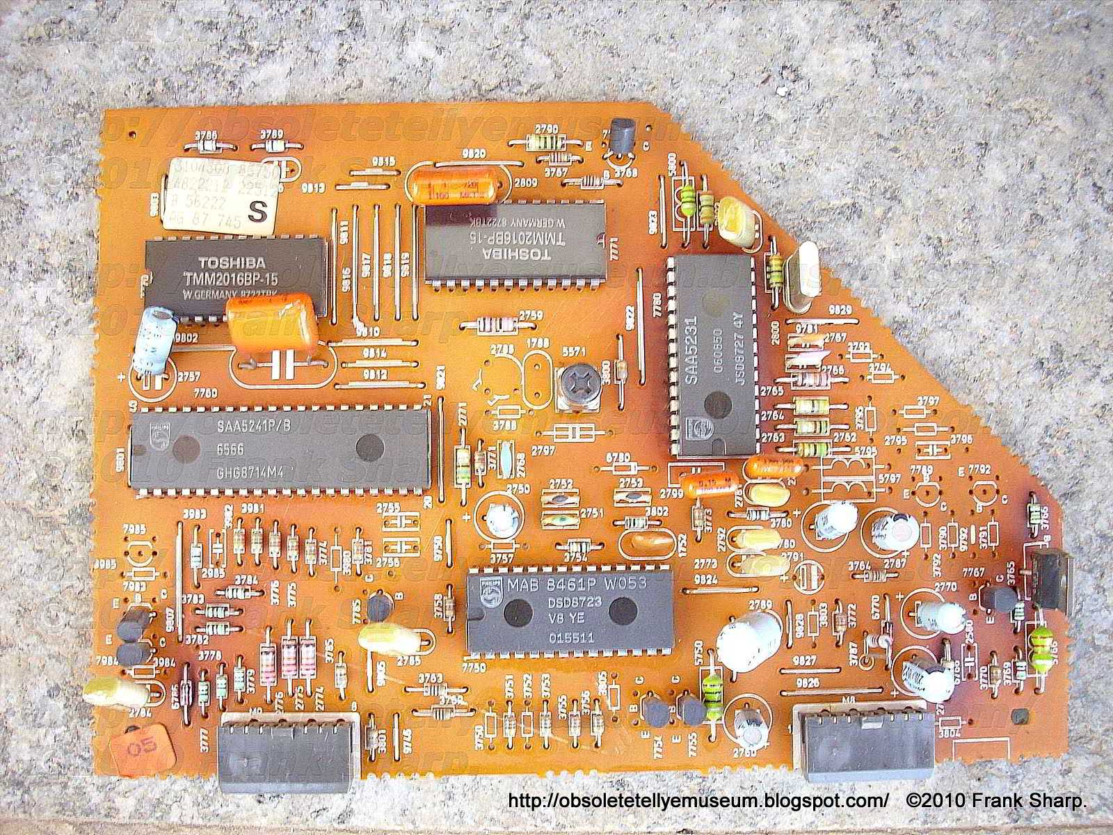


CHASSIS 3A UNITS VIEW.
- VIDEO CHROMA UNIT: 3104 308 83790
TDA4580 + TDA4555 + TDA4565
- TELETEXT UNIT: 3104 308 86750
SAA5231 + SAA5241 + MAB8461
- SOURCE SELECT + SOUND UNIT: 3104 308 83650
TDA8405
- POWER SOUND AMPLIFIER UNIT: 3104 308 02960
PHILIPS TDA1514A 50 W high performance hi-fi amplifier
GENERAL DESCRIPTION
The TDA1514A integrated circuit is a hi-fi power amplifier for use as a building block in radio, tv and other audio
applications. The high performance of the IC meets the requirements of digital sources (e.g. Compact Disc equipment).
The circuit is totally protected, the two output transistors both having thermal and SOAR protection (see Fig.3). The circuit
also has a mute fun
ction that can be arranged for a period after power-on with a delay time fixed by external components.The device is intended for symmetrical power supplies but an asymmetrical supply may also be used.
Features
· High output power
· Low harmonic distortion
· Low intermodulation distortion
· Low offset voltage
· Good ripple rejection
· Mute/stand-by facilities
· Thermal protection
· Protected against electrostatic discharge
· No switch-on or switch-off clicks
· Very low thermal resistance
· Safe Operating Area (SOAR) protection.
QUICK REFERENCE DATA
PACKAGE OUTLINE
9-lead SIL, plastic power (SOT131R); SOT131-2; 1996 July 19.
PARAMETER CONDITIONS SYMBOL MIN. TYP. MAX. UNIT
Supply voltage range
(pin 6 to pin 4) VP ± 10 - ±30 V
Total quiescent current VP = ± 27.5 V Itot - 56 - mA
Output power THD = -60 dB;
VP = ± 27.5 V;
RL = 8 W Po - 40 - W
VP = ± 23 V;
RL = 4 W Po - 48 - W
Closed loop voltage gain determined
externally Gc - 30 - dB
Input resistance determined
externally Ri - 20 - kW
Signal plus noise-to-noise ratio Po = 50 mW (S+N)/N - 83 - dB
Supply voltage ripple
rejection f = 100 Hz SVRR - 64 - dB
PHILIPS TDA4555 Multistandard decoderGENERAL DESCRIPTION
The TDA4555 and T
DA4556 are monolithic integratedmultistandard colour decoders for the PAL, SECAM,
NTSC 3,58 MHz and NTSC 4,43 MHz standards. The
difference between the TDA4555 and TDA4556 is the
polarity of the colour difference output signals (B-Y)
and (R-Y).
Features
Chrominance part
· Gain controlled chrominance amplifier for PAL, SECAM
and NTSC
· ACC rectifier circuits (PAL/NTSC, SECAM)
· Burst blanking (PAL) in front of 64 ms glass delay line
· Chrominance output stage for driving the 64 ms glass
delay line (PAL, SECAM)
· Limiter stages for direct and delayed SECAM signal
· SECAM permutator
Demodulator part
· Flyback blanking incorporated in the two synchronous
demodulators (PAL, NTSC)
· PAL switch
· Internal PAL matrix
· Two quadrature demodulators with external reference
tuned circuits (SECAM)
· Internal filtering of residual carrier
· De-emphasis (SECAM)
· Insertion of reference voltages as achromatic value
(SECAM) in the (B-Y) and (R-Y) colour difference output
stages (blanking)
Identification part
· Automatic standard recognition by sequential inquiry
· Delay for colour-on and scanning-on
· Reliable SECAM identification by PAL priority circuit
· Forced switch-on of a standard
· Four switching voltages for chrominance filters, traps
and crystals
· Two identification circuits for PAL/SECAM (H/2) and
NTSC
· PAL/SECAM flip-flop
· SECAM identification mode switch (horizontal, vertical
or combined horizontal and vertical)
· Crystal oscillator with divider stages and PLL circuitry
(PAL, NTSC) for double colour subcarrier frequency
· HUE control (NTSC)
· Service switch.
PHILIPS TDA4565 Colour transient improvement circuit
GENERAL DESCRIPTION
The TDA4565 is a monolithic integrated circuit for colour transient improvement (CTI) and luminance delay line in gyrator
technique in colour television receivers.
Features
· Colour transient improvement for colour difference signals (R-Y) and (B-Y) with transient detecting-, storage- and
switching stages resulting in high transients of colour difference output signals
· A luminance signal path (Y) which substitutes the conventional Y-delay coil with an integrated Y-delay line
· Switchable delay time from 730 ns to 1000 ns in steps of 90 ns and additional fine adjustment of 50 ns
· Two Y output signals; one of 180 ns less delay.
PHILIPS TDA4580 Video control combination circuit with automatic cut-off control:
GENERAL DESCRIPTION
The TDA4580 is a monolithic integrated circuit which
performs video control functions in television receivers
with a colour difference interface. For example it operates
in conjunction the multistandard colour decoder TDA4555.
The required input signals are: luminance and negative
colour difference −(R-Y) and −(B-Y), and a 3-level
sandcastle pulse for control purposes. Analogue RGB
signals can be inserted from two sources. One with full
performance adjustment possibilities. RGB output signals
are available for driving the video output stages. This
circuit provides automatic cut-off control of the picture
tube.
Features
• Capacitive coupling of the colour difference, luminance
and RGB input signals with black level clamping
• Two sets of analogue RGB inputs via fast switch 1 and
fast switch 2
• First RGB inputs and fast switch 1 in accordance with
peritelevision connector specification
• Saturation, contrast and brightness control acting on
first RGB inputs
• Brightness control acting on second RGB inputs
• Equal black levels for television and inserted signals
• Clamping, horizontal and vertical blanking, and timing of
automatic cut-off, controlled by a 3-level sandcastle
pulse
• Automatic cut-off control with compensation for leakage
current of the picture tube
• Measuring pulses of cut-off control start immediately
after end of vertical part of sandcastle pulse
• Three selectable blanking intervals for PAL, SECAM
and NTSC/PAL-M
• Two switch-on delays for run-in without discolouration
• Adjustable peak drive limiter
• Average beam current limiter
• G-Y and RGB matrix coefficients selectable for
PAL/SECAM and NTSC (correction for FCC primaries)
• Bandwidth 10 MHz (typ.)
• Emitter-follower o
utputs for driving the RGB outputstages.
Notes to the characteristics
1.
Maximum 8 V.
2.
The value of the colour difference input signals, −(B-Y) and −(R-Y), is given for saturated colour bar with 75% of
maximum amplitude.
3.
Capacitive coupled to a low ohmic source; recommended value 600 Ω (max.).
4.
At pin 19 for V19-24≤ 2,0 V, no further decrease of contrast is possible.
5.
The peak drive limiting of output signals is achieved by contrast reduction. The limiting level of the output signals is
equal to the voltage V9-24, adjustable in the range 5 to 11 V. After exceeding the adjusted limiting level at peak drive
limiter will not be active during the first line.
6.
The average beam current limiting acts on contrast and at minimum contrast on brightness (the external contrast
voltage at pin 19 is not affected).
7.
At nominal brightness the black level at the output is 0,3 V (≅ −10% of nominal signal amplitude) below the measuring
level.
8.
The internal control voltage can never be more positive than 0,7 V above the internal contrast voltage.
9.
Matrix equation
a) V(R-Y),V(B-Y): output of NTSC decoder of PAL type demodulating axis and amplitudes
b) V(G-Y)(1), V(R-Y) (note 1), V(B-Y) (note 1): for NTSC modified CD signals; equivalent to demodulation with the
following axes and amplification factors:−
c) (B-Y)(1) demodulator axis: 0°
d) (R-Y)(1) demodulator axis: 115° (PAL 90°)
e) (R-Y)(1) amplification factor: 1,97 (PAL 1,14)
f) (B-Y)(1) amplificati
on factor: 2,03 (PAL 2,03)g) V(G-Y)(1) = −0,27 V(R-Y)(1)− 0,22 V(B-Y)(1).
10. During clamping time, in each channel the black level of the inserted signal is clamped on the black level of the
internal signal behind the matrix (dependent on brightness control).
11. During warm-up time of the picture tube, the RGB outputs (pins 1, 3 and 5) are blanked to minimum output voltage.
An inserted white pulse during the vertical flyback is used for beam current detection. If the beam current exceeds
the threshold of the warm-up detector at pin 26, the cut-off current control starts operating, but the video signal is still
blanked. After run-in of the cut-off current loop, the video signal will be released.
The first measuring pulse occurs in the first complete line after the end of the vertical part of the sandcastle pulse.
The absolute minimum vertical part must contain 9 line-pulses. The cycle time of the counter is 63 lines. When the
vertical pulse is longer than 61 lines, the IC is reset to the switch-on condition. In this event the video signal is blanked
and the RGB-outputs are blanked to minimum output voltage as during warm-up time.
During leakage current measurement, all three channels are blanked to ultra-black level 1. With the measuring level
only in the controlled channel, the other two channels are blanked to ultra-black level 1.
The brightness control shifts both the signal black level and the ultra-black level 2. The brightness control is disabled
from line 4 to the end of the last measuring line (see Fig.4).
With the most adverse conditions (maximum brightness and minimum black level 2) the blanking level is located 30%
of nominal signal amplitude below the cut-off measuring level.
12. The given blanking times are valid for the vertical part of the sandcastle pulse of 9 to 15 lines. If the vertical part is
longer and the cut-off lines are outside the vertical blanking period of 18, 22 or 25 lines respectively, the blanking of
the signal ends with the end of last of the three cut-off measuring pulses as shown in Fig.7.
13. The sandcastle pulse is compared with three internal thresholds (proportional to VP) to separate the various pulses.
The internal pulses are generated when the input pulse at pin 10 exceeds the thresholds. The thresholds are for:
a) Horizontal and vertical blanking
V10-24= 1,5 V
b) Horizontal pulse
V10-24= 3,5 V
c) Clamping pulse
V10-24= 7,0 V
14. The outputs at pins 1, 3 and 5 are emitter followers with current sources and emitter protection resistors.
15. The value of the cut-off control range for the positive RGB output signals is given for a nominal output signal. If the
signal amplitude is reduced, the cut-off range can be increased.
16. The gain data is given for a nominal setting of the contrast and saturation controls, measured without load at the RGB
outputs (pins 1, 3 and 5).
PINNING
PIN NO.
MNEMONIC
DESCRIPTION
1
R0
Red output
2
CR
Red storage capacitor for
cut-off control
3
G0
Green output
4
CG
Green storage capacitor for
cut-off control
5
B0
Blue output
6
VP
Positive supply voltage
(+ 12 V)
7
CB
Blue storage capacitor for
cut-off control
8
LD
PAL/NTSC matrix and
blanking time level detector
input
9
PDL
Peak drive limiting input
10
SC
Sandcastle pulse input
11
FSW1
Fast switch 1 for Y, CD and
RGB inputs
12
B1
Blue input (external signal)
13
G1
Green input (external signal)
14
R1
Red input (external signal)
15
Y
Luminance input
16
SAT
Saturation control input
17
−(R-Y)
Colour difference input −(R-Y)
18
−(B-Y)
Colour difference input −(B-Y)
19
CON
Contrast control input
20
BRI
Brightness control input
21
B2
Teletext blue input
22
G2
Teletext green input
23
R2
Teletext red input
24
GND
Ground
25
BCL
Average beam current limiting
input
26
CC
Automatic cut-off control input
27
CLC
Storage capacitor for leakage
current
28
FSW2
Fast switch 2 for teletext
inputs
PHILIPS CHASSIS 3A Circuit arrangement for identifying the transmission standard of a color television signal:
A circuit arrangement for identifying the transmission standard of a color television signal, having a chrominance subcarrier upon which chrominance information is modulated and color synchronising pulses, includes circuitry (14, 21, 24, 25) for determining the frequency of the chrominance subcarrier which, in those cases in which a given standard of the color television signal can unambiguously be concluded from the determined chrominance subcarrier frequency of the color television signal to be decoded, the decoder is immediately switched to the decoding of this signal of this standard, and in addition includes circuitry (23, 22) which determine the vertical deflection frequency of the television signal and ascertain whether the chrominance subcarrier has a line-sequentially alternating phase, and that in those cases in which the determined chrominance subcarrier frequency cannot unambiguously be assigned to a given standard, these information components are also used for identifying the standard of the color television signal to be decoded and for adjusting the decoder to this standard, in addition to the chrominance subcarrier frequency.
1. A circuit arrangement in a color decoder for identifying the transmission standard of a color television signal comprising color synchronizing pulses and a chrominance subcarrier upon which chrominance information is modulated, characterized in that the circuit arrangement comprises:
means for determining a frequency of the chrominance subcarrier and, when the frequency alternates from line to line of the color television signal, for determining a means average of the two chrominance subcarrier frequencies;
first means, coupled to said means for determining the frequency or averaged frequency to the chrominance subcarrier, for identifying the television standard of the color television signal when said determined or averaged chrominance subcarrier frequency accurately corresponds to that of one of the transmission standards to be identified even when the measuring inaccuracy occurring during the determination of the chrominance subcarrier frequency is taken into account;
means for determining the vertical deflection frequency of the television signal, for ascertaining whether the chrominance subcarrier has a line-sequentially alternating phase, and for determining said alternating phase;
second means, coupled to said means for determining the vertical deflection frequency, for identifying the transmission standard of the color television signal by using information on the vertical deflection frequency and whether the chrominance subcarrier has a line-sequentially alternating phase; and
means for switching said color decoder to one of said transmission standards in response to one of said first and second identifying means.
2. A circuit arrangement as claimed in claim 1, wherein said color decoder is a digital color decoder and includes, for demodulating the color information components, a quadrature mixer and a mixer oscillator, characterized in that said first identifying means comprises:
a phase demodulator for receiving difference signals produced by said quadrature mixture;
a differentiator coupled to an output of said phase demodulator for generating a difference signal, during the occurrence of the color synchronizing pulses, indicating the difference frequency between the mixer oscillator frequency and the averaged chrominance subcarrier frequency of the color television signal;
means for producing an offset signal indicating the difference frequency between a preset, fixed standard frequency and the adjusted mixer oscillator frequency; and
means for adding together said difference signal and said offset signal taking into account the signs of said difference and offset signals, the value of this sum signal indicating the difference frequency between the averaged chrominance subcarrier frequency of the color television signal to be decoded and the standard frequency.
3. A circuit arrangement as claimed in claim 1, characterized in that the means for determining the alternating phase of the chrominance subcarrier include a phase detector which, in the case of a line-sequentially alternating phase of the chrominance subcarrier, determines the alternating phase. 4. A circuit arrangement as claimed in claim 1, characterized in that said means for determining the vertical deflection frequency of the color television signal comprises a counter for counting the number of lines of the color television signal between two vertical synchronizing pulses, the vertical deflection frequency of the color television signal being determined from the number of lines counted. 5. A circuit arrangement as claimed in claim 2, characterized in that the standard frequency is chosen such that it represents approximately an average value of the different chrominance subcarrier frequencies of the television standards to be identified. 6. A circuit arrangement as claimed in claim 2, characterized in that the output signal of the phase demodulator is also used in the color decoder for a readjustment of the phase of the output signal of the mixer oscillator. 7. A circuit arrangement as claimed in claim 2, characterized in that several television standards having chrominance subcarrier frequencies which are very near to each other are combined into one standards group, wherein said means for determining the frequency of the chrominance subcarrier of the color television signal is only effected with such an accuracy that it can be determined to which standards group the television signal to be decoded belongs, and wherein for the identification of the correct television standard within the standards group, the means for determining the vertical deflection frequency and also the phase behavior of the chrominance subcarrier are used. 8. A circuit arrangement as claimed in claim 7, characterized in that for a standards group, only one common offset signal is generated in such a manner that when the mixer oscillator is adjusted to one of the chrominance subcarrier frequencies of the standard of this group, the offset signal indicates the difference frequency between the preset fixed standard frequency and an average value of the chrominance subcarrier frequencies of the standards of this group. 9. A circuit arrangement as claim in claim 8, characterized in that the evaluation of the sum signal of the difference signal and the offset signal is only effected with such an accuracy that it can be determined to which standards group the color television signal belongs. 10. A circuit arrangement as claimed in claim 1, characterized in that the color television signal is a digital signal and the circuit arrangement for identifying the transmission standard is a digital circuit arrangement.
Description:
BACKGROUND OF THE INVENTION
1. Field of the Invention
The invention relates to a circuit arrangement for identifying in a color decoder, the transmission standard of a color television signal comprising a chrominance subcarrier upon which chrominance information is modulated, and synchronizing pulses.
 For color television signals, there is an abundance of different transmission standards which differ from each other more specifically in the manner in which the chrominance information components are transmitted. These chrominance information components are modulated on a chrominance subcarrier which however may have different frequencies depending on the standard and which in addition may have a frequency which alternates from picture line to picture line of the color television signal. The chrominance information components themselves are also modulated in different manners. For color decoders which must be suitable for decoding color television signals of different transmission standards, this causes the problem that the color decoders must not only be suitable for decoding the different transmission standards but that they must also be capable of recognizing which transmission standard the color television signal to be decoded has.
2. Description of the Related Art
Known circuit arrangements for identifying the transmission standard of color television signals generally operate in an iterative manner, that is to say they first switch to any random standard, then check whether the color decoder is capable of decoding and switching the chrominance information components and, if not, switch to a subsequent standard. This procedure is continued until the color decoder is switched to a transmission standard for which a correct decoding of the chrominance information components of the color television signal is effected. Thus, in this procedure a given transmission standard is not immediately identified but the correct transmission standard is ultimately determined by testing different decodings. This requires a certain period of time which, particularly also in the case of short interruptions or interferences of the color television signal may be displayed in an annoying manner, since the search procedure starts again from the beginning after each interruption.
SUMMARY OF THE INVENTION
The invention has for its object to provide a circuit arrangement of the type defined in the opening paragraph, which allows an immediate identification of the transmission standard of a color television signal to be decoded.
According to the invention, this object is achieved in that means for determining the frequency of the chrominance subcarrier are provided which, at a frequency which alternates from line to line of the color television signal, determine the average value of the two chrominance subcarrier frequencies, that in those cases in which the determined and optionally averaged chrominance subcarrier frequencies can accurately be assigned to precisely one of the transmission standards to be identified even when the measuring inaccuracy occurring during the determination of the chrominance subcarrier frequency is taken into account, the decoder is immediately switched to the decoding of the signal of this standard, that furthermore means are provided which determine the vertical deflection frequency of the television signal and ascertain whether the chrominance subcarrier has a line-sequential alternating phase, and that means are provided which in those cases in which, the determined and possibly averaged chrominance subcarrier frequency cannot unambiguously be assigned to a given standard, utilize this information to identify the standard of the color television signal to be decoded and adjust the decoder to the identified standard.
As stated in the foregoing, the different transmission standards for color television signals differ more specifically in the fact that the chrominance subcarrier has different frequencies. In addition, some standards have a chrominance subcarrier frequency which alternates from picture line to picture line of the color television signal. In this case a mean value of the two chrominance subcarrier frequencies is determined.
 Some transmission standards now have a chrominance subcarrier frequency or a mean value of the two chrominance subcarrier frequencies, respectively, in whose neighborhood no chrominance subcarrier frequencies of other standards are present. In these cases, it is possible to determine the transmission standard present immediately from the determined chrominance subcarrier frequency. However, there are actually very many further transmission standards having identical or closely adjacent chrominance subcarrier frequencies. In these cases, it is not sufficient to determine only the chrominance subcarrier frequency, particularly as the measuring inaccuracy during the determination of the chrominance subcarrier frequency in these cases does not allow a definite conclusion as regards the transmission standard present, as it is not sure which one of the very closely adjacent chrominance subcarrier frequencies contains the color television signal to be decoded. It is therefore provided in these cases to additionally determine whether the chrominance subcarrier has a phase relationship which alternates line sequentially and which vertical deflection frequency is provided in accordance with the color television signal to be decoded. There are then consequently three parameters available, namely the determined chrominance subcarrier frequency, the phase behavior of the chrominance subcarrier and the vertical deflection frequency. On the basis of these three parameters, it is possible to determine the present transmission standard in those cases in which no unambiguous conclusion can be drawn from the determined chrominance subcarrier frequencies as regards a given transmission standard.
In this circuit arrangement, the determination of the transmission standard of the color television signal is consequently effected by determining different parameters of the signal itself, so that an immediate identification of the transmission standard is possible, without the necessity of "testing out" the coding. A fast identification of the transmission standard present is consequently achieved. Because of the fact that two further parameters are utilized in those cases in which it is not possible to determine unambiguously from the determined and averaged chrominance subcarrier frequency, which averaging is effected if the chrominance subcarrier frequency alternates, what transmission standard is present, an adequate noise immunity during the identification is also obtained.
In accordance with an embodiment of the invention, the circuit arrangement in a color decoder in which for the demodulation of the chrominance information components a quadrature mixer and a mixer oscillator are provided, is characterized in that to determine the optionally averaged frequency of the chrominance subcarrier, a phase demodulator is provided to which the difference signals produced in the quadrature mixer are applied and which is followed by a differentiator producing a difference signal which, during the occurrence of the color synchronizing pulses, indicates the difference frequency between the mixer oscillator frequency and the optionally averaged chrominance subcarrier frequency of the color television signal, that means for generating an offset signal are provided which indicate the difference frequency between a preset, fixed standard frequency and the preset mixer oscillator frequency, that the difference signal and the offset signal are added together taking their sign into account, the value of this sum indicating the difference frequency between the optionally averaged chrominance subcarrier frequency of the color television signal to be decoded and the standard frequency.
Since the chrominance information components are modulated upon a chrominance subcarrier, it is necessary for the processing of the color information components in, for example, a color television receiver, to demodulate these color information components again, that is to say to reset them again to the baseband. As the color information components are modulated upon the chrominance subcarrier in essentially all the transmission standards in the form of two color difference signals having different phase and/or frequencies, this demodulation occurs in the color decoder in general, at least in some standards, by means of a quadrature mixer, to which the color television signals to be decoded and the output signal of a mixer oscillator are applied. The mixer oscillator must then oscillate at the frequency of the chrominance subcarrier or at a defined frequency between two chrominance subcarrier frequencies which alternate from line to line. This is however only ensured when the correct transmission standard was previously identified. If this is not the case, then the mixer oscillator operates at any different frequency, for example at the chrominance subcarrier frequency of an other transmission standard.
To determine the frequency of the chrominance subcarrier of the available color television signal to be decoded, it is provided for the circuit arrangement in accordance with the invention, that the difference signals produced in the quadrature mixer are applied to a phase demodulator which itself is followed by a differentiator. This differentiator produces a frequency-proportional signal which, during the color synchronizing pulses provided in the color television signals indicate the difference frequency between the mixer oscillator frequency and the optionally averaged chrominance subcarrier frequency of the color television signal. Should the mixer oscillator already have been adjusted to the correct frequency of the chrominance subcarrier of the color television signal to be decoded, then this difference frequency has zero value, that is to say the two color difference signals have already been converted to the baseband. If however the correct color television standard has not yet been identified or the mixer oscillator does not operate at the frequency of the chrominance subcarrier of the color television signal present, then the color difference signals are not converted to the baseband but a conversion to a carrier of another frequency takes place. In this case, the differentiator then supplies an output signal which indicates the difference frequency between the mixer oscillator frequency and the chrominance subcarrier frequency of the television signal. For a signal having a line-sequentially alternating chrominance subcarrier frequency, this signal has values which change from line to line and are averaged.
In addition, means for generating an offset signal are provided. This offset signal is based, on the one hand, on a preset, fixed standard frequency and, at the other hand, on the adjusted mixer oscillator frequency, which is indeed known. The offset signal represents the difference frequency between this standard frequency and the adjusted mixer oscillator frequency.
Both the difference signal and also the offset signal are added together, taking the occurring sign into account. Thus a sum signal is obtained which indicates the difference frequency between the averaged chrominance subcarrier frequency of the color television signal to be decoded and the standard frequency. Since the standard frequency has a fixed value, the chrominance subcarrier frequency can immediately be decided from this sum value. Consequently, this sum value can directly be used for the appropriate setting of the frequency of the mixer oscillator. This is however only effected when this frequency occurs only at a predetermined transmission standard. If this is not the case, then, as described in the foregoing, the further parameters, phase behavior of the chrominance subcarrier and vertical deflection frequency, are also used.
Determining the phase behavior of the chrominance subcarrier, i.e. the determination whether it alternates as regards its phase from picture line to picture line, is advantageously possible in that, as is provided in accordance with a further embodiment of the invention, the means for determining the alternating phase of the chrominance subcarrier include a phase detector which, in the case of an alternating phase of the chrominance subcarrier, determines the from line to line differing phase from line to line.
In accordance with a further embodiment of the invention, it is provided that to determine the vertical deflection frequency of the color television signal, a counter is provided which counts the number of lines of the color television signal between two vertical synchronizing pulses, and that a conclusion is drawn from the line number thus obtained as regards the vertical deflection frequency of the color television signal.
The vertical deflection frequency can indirectly be obtained in that it is determined how many picture lines occur in the color television signal to be decoded between two vertical synchronizing pulses. In all the existing color television standards, it is a fact that signals having a 50 Hz vertical frequency have 625 lines and signals having a 60 Hz vertical deflection frequency have 525 lines per pictures. Thus the vertical deflection frequency present can be determined from the line number of a picture.
In accordance with an embodiment of the invention, it is provided that the standard frequency is chosen such that it approximately represents an average value of the different chrominance subcarrier frequencies of the standards to be identified. Such a choice of the standard frequency is advantageous as then the offset signal assumes relatively low values.
In general, a phase demodulator is always provided in the color decoders, to which the demodulated color difference signals are applied, to readjust the mixer oscillator as regards its phase relative to the phase of the chrominance subcarrier. Such a phase demodulator included in the decoder for the phase control can however, as is provided in a further embodiment of the invention, also be simultaneously used in the circuit arrangement according to the invention to determine the difference signal.
In accordance with a further embodiment of the invention, it is provided that several standards having chrominance subcarrier frequencies which are very near to each other are combined into one standard group, that the determination of the frequency of the chrominance subcarrier of the color television signal is only effected with such an accuracy that it can be determined to which color standard group the television signal to be decoded belongs, and that for the identification of the correct standard within the standard group, the vertical deflection frequency obtained and also the phase behavior of the chrominance subcarrier are used.
Several of the known transmission standards for color television signals have chrominance subcarrier frequencies which are very near to each other. In these cases, the identification of the standard is critical, as the frequencies of the chrominance subcarrier can fluctuate. In such cases, the obtained and optionally averaged frequency of the chrominance subcarrier is advantageously not directly used for the determination of the transmission standard, but the phase behavior of the chrominance subcarrier and the vertical deflection frequency are also used. Since an unambiguous identification of the transmission standard present is not possible without further measures in such standards having chrominance subcarrier frequencies which are very near to each other, these transmission standards can advantageously be combined into one standards group. The determination of the frequency of the chrominance subcarrier of the color television signal must then only be effected with such an accuracy that it is determined whether a color television signal present belongs to this standard group or not, i.e. the circuit arrangement must consequently operate with only such an accuracy during the determination of the frequency of the chrominance subcarrier, that it can be determined whether the frequency of a chrominance subcarrier is located in the frequency range which is covered by the chrominance carriers of the different standards of this group.
For the generation of the above-described offset signal, this means that, as is provided in accordance with a further embodiment of the invention, only one common offset signal is generated for a standards group in a manner such that when the mixer oscillator is adjusted to one of the chrominance subcarrier frequencies of the standard of this group, the offset signal indicates the difference frequency between the preset, fixed standard frequency and an average value of the chrominance subcarrier frequencies of the standards of this group.
As in the above-described case, the determination of the frequency of the chrominance subcarrier must only be effected with an adequate accuracy for the identification of standards group, it is sufficient for the offset signal not to be generated separately for each transmission standard of this group but that rather a common offset signal is produced which indicates the difference between the preset, fixed standard frequency and an average valve of the chrominance subcarrier frequencies of the standards of each respective group. The sum signal described in the foregoing then still has an adequate accuracy to allow the determination whether the chrominance subcarrier frequency of a color television signal to be decoded is included in the frequency range of the chrominance subcarrier of a standards group or not.
Also the evaluation of the sum signal of the difference signal and the offset signal needs, as is provided in accordance with a further embodiment of the invention, only to be effected with such an accuracy that it can be determined to which standards group the color television signal belongs.
In all those cases in which the determination of the optionally averaged frequency of the chrominance subcarrier is effected with only such an accuracy that it belongs to one of the standards groups, the identification of the transmission standard present is effected with the aid of two further parameters, namely the determination whether the chrominance carrier alternates as regards its phase from picture line to picture line, and which vertical deflection frequency is present. On the basis of the three parameters then available, namely the association of the chrominance subcarrier frequency with a given standards group and the further two parameters, the transmission standard present is then obtained. As soon as this standard has been determined, an adjustment of the color decoder to the exact chrominance subcarrier frequency of the standard present is then possible.
In accordance with a further embodiment of the invention, it is provided that the color television signal is a digital signal and the circuit arrangement for identifying the transmission standard a digital circuit arrangement. The circuit arrangement in accordance with the invention can be used with special advantage for a digital television signal as it operates with circuit elements which can be easily realized digitally.
BRIEF DESCRIPTION OF THE DRAWING
An embodiment of the invention shown in the sole Figure, in the form of a block circuit diagram, in the accompanying drawing, will now be described in greater detail hereinafter.
DESCRIPTION OF THE PREFERRED EMBODIMENT
The block circuit diagram shown in the Figure includes a digital color decoder comprising the circuit arrangement of the invention which also operates digitally, for identifying the transmission standard of a digital color television signal.
In the Figure, the blocks enclosed with a dotted line represent the circuit elements which are necessary for the circuit arrangement of the subject invention. The remaining blocks are typical in a color decoder. As will be described in greater detail hereinafter, some of the remaining blocks of the color decoder which are anyhow included in the decoder, are additionally utilized in the identification of the transmission standard.
Either a pure chrominance signal modulated on a chrominance subcarrier or a complete color television signal containing the luminance signal, chrominance information components modulated on a chrominance subcarrier, blanking periods and also synchronizing pulses, consequently what is commonly denoted the composite color signal, may be applied to a multiplexer 1 of the decoder in accordance with the Figure, arranged at the input side.
In a high-pass filter 2 arranged subsequent to the multiplexer 1, the luminance signal portions of a composite color signal, more specifically the relatively low frequency portions of this signal are suppressed. This high-pass filter must, however, be designed such that the chrominance subcarrier and any occurring sidebands are not yet suppressed. The high-pass filter 2 is followed by a quadrature mixer 3 to which furthermore the output signal of a mixer oscillator 4 is applied. A demodulation of the chrominance information components modulated on a chrominance subcarrier must be effected in the quadrature mixer 3. To that end, as will be described hereinafter, the oscillator frequency of the mixer oscillator 4 is to be adjusted to the frequency of the chrominance subcarrier of the color television signal to be decoded. A quadrature mixer is required as the chrominance information component in some transmission standards are modulated on a chrominance subcarrier in the form of two color difference signals having different phases. These two color difference signals are then demodulated in the quadrature mixer 3.
Since in the quadrature mixer 3 not only the desired difference signals representing the demodulated color difference signals, but also the corresponding sum signals occur, the quadrature mixer 3 is followed by a low-pass filter 5 which suppresses the sum signal produced in the mixer 3. This low-pass filter 5 is followed by a variable-gain amplifier 6, which has for its object to maintain the chrominance signals in the decoder at a nominal value. The amplifier 6 is followed by a further low-pass filter 7 which has the same object as the low-pass filter 5. The color difference signals outputted by the low-pass filter 7 are applied to a line-delay device 8 which, depending on the transmission standard present, performs a line-wise delay of the chrominance information components. At the output of the line delay device 8 the two color difference signals are then for example simultaneously available at the transmission of a SECAM signal, or available free from phase errors at the transmission of a PAL signal.
In this color decoder, shown in the Figure, it is necessary, for signals of those transmission standards in which the chrominance information components are amplitude-modulated on a chrominance subcarrier, that a readjustment of the phase of the output signal of the mixer oscillator relative to the phase of the chrominance subcarrier of the color television signal is continuously effected. In addition thereto, an amplitude control must be effected for signals of all the transmission standards. This phase or amplitude control is effected by means of the following circuit blocks:
The output signal of the low-pass filter 7 is applied to a chrominance carrier-deemphasis filter 9 which only acts on SECAM signals. This filter is commonly denoted as a "Cloche filter". A phase demodulator 10 which does not only effect a phase demodulation but also an amplitude detection of the color difference signals applied thereto, is arranged subsequent to the filter 9. Consequently the phase demodulator 10 supplies two output signals which represent indications as regards their phase and their amplitude. These signals are applied to a color synchronizing pulse detector 11 which evaluates the signals applied to it by the phase demodulator 10 during those periods of time in which a color synchronizing pulse occurs in the color difference signals, as only these color synchronizing pulses have a defined phase and a defined level. The color synchronizing pulse detector 11 compares the amplitude information supplied by the phase modulator 10 during the color synchronizing pulses to a nominal amplitude value and, when they deviate from this nominal value, applies corresponding signals to an amplitude loop filter 12. The output signal of this loop filter 12 is used to control the gain factor of the amplifier 6. The structure of the amplitude loop filter 12 determines the readjustment behavior of the overall assembly as regards the amplitude.
In addition, an evaluation of the phase of the chrominance carrier is effected during those periods of time in which a color synchronizing pulse occurs in the color difference signals. These signals are applied to a phase-loop filter 13. The output signals of the filter 13 are applied to the chrominance carrier oscillator 4 which, as regards the phase of its output signal, is controlled by these signals. The design of the phase-loop filter 13 determines the readjustment behavior of the circuit arrangement as regards the phase of the output signal of the mixer oscillator 4.
The signals produced by the phase demodulator 10 are further applied to a differentiator 14 whose output signal is applied, on the one hand, to the color synchronizing pulse detector 11 and, on the other hand, to a SECAM-video deemphasis filter 15, which has for its purpose to effect the video deemphasis provided in accordance with the SECAM standard. The output signals of the filter 15 are applied to the line delay device 8.
The decoder elements shown in the Figure and described so far are anyhow present in this decoder and in themselves do not allow of an identification of a transmission standard of the color television signal fed into the decoder. For such an identification an arrangement 20 for color standard identification is rather provided.
The arrangement 20 includes a frequency range detector 21 to which the output signals supplied by the differentiator 14 are applied by the color synchronizing pulse detector 11 during those periods of time in which color synchronizing pulses occur in the color difference signals. The frequency range detector 21 consequently receives the output signal from differentiator 14 during each color synchronizing pulse.
The arrangement 20 for color standard identification also includes a phase detector 22 which receives the phase measuring signals supplied by the phase demodulator 10 of the decoder.
The arrangement 20 further includes a vertical-frequency detector 23 which from a synchronizing circuit, not shown in the Figure, receives a signal which indicates when vertical synchronizing pulses occur in the color television signal.
The output signals of the frequency range detector 21, of the phase detector 22 and of the vertical frequency detector 23 are applied to an evaluation unit 24. An output signal of the evaluation unit 24 is applied to an arrangement 25 for the generation of the offset signal, whose output signal is again applied to the frequency range detector 21.
Now the arrangement 20 for color standard identification comprising block elements 21 to 25 will be described in greater detail as regards its mode of operation.
It is assumed that a composite color television signal whose transmission standard is unknown, is applied to the multiplexer I of the decoder. This means with a high degree of probability, that as regards the frequency of its output signal which is applied to the quadrature mixer 3 the chrominance carrier oscillator 4 is not adjusted to the frequency of the chrominance carrier of the color television signal to be decoded. This has for its consequence that the color difference signals are not demodulated but only converted to a different carrier frequency. This again has for its consequence that the phase demodulator 10 detects a continuously changing phase which is converted in the differentiator 14 into a frequency signal which indicates that carrier frequency to which the two color difference signals are now converted by means of the mixer 3. This frequency is identical to the difference frequency between the mixer oscillator frequency and the frequency of the chrominance subcarrier of the color television signal. This signal is evaluated in the color synchronizing pulse detector 11 during those periods of time in which the color difference signals have color synchronizing pulses, as only during these periods of time a defined frequency and phase of the chrominance subcarrier is given. This difference signal thus evaluated is applied to the frequency range detector 21 of the arrangement 20 for the object of color standard identification.
The evaluation unit 24 of the arrangement 20 has previously applied a signal to the chrominance carrier oscillator 4, by means of which a predetermined frequency of the oscillator was set in the chrominance carrier oscillator 4. As has already been described in detail in the foregoing, it must however first be assumed that this frequency is not identical to the frequency of the chrominance subcarrier of the color television signal to be decoded. The evaluation unit 24 applies a signal to the arrangement 25, which indicates to which frequency the chrominance carrier oscillator 4 was set. An offset signal, which indicates the difference frequency between a preset, fixed standard frequency and the set mixer oscillator frequency as indicated by the evaluation unit 24, is produced in the arrangement 25. This standard frequency, which is preset only once and then remains unchanged, is advantageously chosen such that it is approximately halfway the frequency range of the different chrominance subcarrier frequencies of the transmission standards. The offset signal produced in the arrangement 25 is applied to the frequency range detector 21.
In the frequency range detector 21, the sum of the offset signal produced by the arrangement 25 and the difference signal produced by the color synchronizing pulse detector 11 is now taken, in which operation the signs must be taken into account. In addition, in those cases in which the difference signal has values which alternate from picture line to picture line, since the chrominance subcarrier frequency alternates line-sequentially, averaging of the difference signal of two lines is effected. During the sum formation, a signal occurs which indicates the difference frequency between the optionally averaged chrominance subcarrier frequency of the chrominance signal to be decoded and the fixed, known standard frequency. On the basis of this signal which is further conveyed to the evaluation unit 24, this evaluation unit 24 is capable of concluding the optionally averaged chrominance subcarrier frequency of the television signal and from this signal to draw a conclusion about the transmission standard and consequently about the frequency to be adjusted in the oscillator 4, since the frequency of the standard signal is known.
After the evaluation unit 24 has determined that frequency to which the subcarrier oscillator 4 is to be adjusted, this setting of the chrominance carrier oscillator can either be effected immediately or further parameters supplied by the phase detector 22 and the vertical frequency detector 23 can be evaluated. Whether this occurs or not, depends on the fact whether the determined chrominance carrier frequency, to which the oscillator 4 is to be adjusted, is only present in one transmission standard. If so, then the chrominance carrier oscillator can immediately be adjusted to this frequency by means of the evaluation unit 24, as it is unambiguously determined which transmission standard is used.
If the determined chrominance carrier frequency is however present in several transmission standards, or have a plurality of transmission standards chrominance subcarrier frequencies which are very close to this frequency, then the determination of the chrominance subcarrier frequency alone is not yet sufficient. In these cases, the evaluation unit 24 also takes into consideration the signals recovered by the phase detector 22 and the vertical frequency detector 23 for the identification of the transmission standard of the color television signal to be decoded.
The output signal of the phase demodulator 10 is applied to the phase detector 22. From this signal, the phase detector 22 determines whether one of the two color difference signals applied to the phase demodulator 10 has a phase which alternates from picture line to picture line. If so, the phase detector 22 applies a corresponding signal to the evaluation unit 24.
The vertical frequency detector 23 includes a counter, not shown, by means of which the number of picture lines between two vertical synchronizing pulses is counted. From the number of picture lines between these pulses, it is possible to draw immediately a conclusion about the vertical deflection frequency of the color television signal, as all the transmission standards which operate with a deflection frequency of 50 Hz, have a nominal number of 625 lines per full picture, while those transmission standards which operate with a vertical deflection frequency of 60 Hz have a nominal number of 525 lines per full picture. It is therefore immediately possible to draw a conclusion about the vertical deflection frequency of the signal from the number of picture lines per full picture. The vertical frequency detector 23 applies a corresponding signal to the evaluation unit 24.
In those cases in which no immediate unambiguous conclusion about the transmission standard present can be drawn from the determined and optionally averaged frequency of the chrominance subcarrier, the evaluation unit 24 does not only evaluate the determined chrominance carrier frequency but also the signals supplied by the phase detector 22 and the vertical frequency detector 23, i.e. any determined line-sequentially alternating phase of the chrominance subcarrier or the determined vertical deflection frequency, respectively. From these three pieces of information, a conclusion can immediately and unambiguously be drawn in the evaluation unit 24 about the present transmission standard of the color television signal, since the known transmission standards always differ in at least one of the three parameters, and a corresponding signal cannot only be applied to the chrominance carrier oscillator 4, but also, in a manner not shown in the Figure, to certain circuit elements of the color decoder or of other switching elements of a color receiver, not shown in the Figure, for the purpose of adjusting it to the transmission standard present.
As has already been described in the foregoing, there are several color television transmission standards in which very similar chrominance subcarrier frequencies are provided. As these chrominance subcarrier frequencies can moreover also fluctuate in actual practice, it is possible that in those cases or when the signals are disturbed by noise, there are difficulties in identifying the standard. In these cases it is advantageous to combine several of these transmission standards into one standards group. For the circuit arrangement shown in the Figure this actually means that in the arrangement 25 only one common offset signal is generated for producing the offset signal for such a standards group. This consequently means that, when, by means of the evaluation unit 24, one of the chrominance subcarrier frequencies of these standards group was adjusted in the chrominance carrier oscillator 4, the arrangement 25 generates only one offset signal independent of the fact which of the chrominance subcarrier frequencies of the standards of this group was adjusted. This offset signal is structured such that it indicates the difference frequency between the preset fixed standard frequency and a mean value of the chrominance subcarrier frequency of the standards of this group. Consequently for all the chrominance subcarrier frequencies of this standards group adjusted in the chrominance carrier oscillator 4 only one common offset signal is produced. Additionally it can be provided in the frequency range detector 21 that the calculation of the sum value of the offset signal supplied by the arrangement 25 and of the difference signal supplied by the phase detector is effected only less accurately. In any case, when such a standards group formation is provided, the determination of the optionally averaged frequency of the chrominance subcarrier of the chrominance auxiliary signal fed into the detector is only effected with such an accuracy that it can be determined to which standards group the color television signal belongs. Consequently, it is then no longer necessary to determine the exact frequency of the chrominance subcarrier of the fed-in color television signal, but it is sufficient to determine whether the frequency of the chrominance subcarrier is included in the frequency range of the chrominance subcarrier of a standards group. In these cases, in additionto the evaluation of the frequency range, it is furthermore recommendable to evaluate the phase behavior of the chrominance carrier and the vertical deflection frequency. This procedure has the advantage that the determination of the frequency of the chrominance subcarrier fed into the decoder can be effected with a reduced accuracy, which accuracy must however still be sufficient to recognize to which standards group the fed-in signal belongs.
For the following color television transmission standards, the above-mentioned formation of standards groups can be effected in, for example, the following manner:
In this example the chrominance subcarriers of the transmission standard of the first group have the same frequency, namely 4.4 MHz. When such a frequency of the chrominance subcarrier is found, it is however not yet clear which of the transmission standards of the first group is present. These signals can however be distinguished by the further parameters. Thus, the PAL signal has a chrominance subcarrier phase which alternates from picture line to picture line. The two NTSC signals have constant phases of the chrominance subcarrier, but they differ as regards the vertical deflection frequency.
The transmission standards of the second group have indeed different frequencies of the chrominance subcarriers, but they are so near to each other than an unambiguous identification is not always ensured, more specifically when the frequencies of the chrominance subcarriers fluctuate. For that reason in this case, the further parameters such as the phase behavior of the chrominance carrier and the vertical deflection frequency are also used.
If in addition to these six transmission standards also the, for example, SECAM standard must be identified, in which the chrominance subcarrier during the color synchronizing pulse has a line-sequentially alternating frequency of 4.25 MHz or 4.406 MHz, then this transmission standard must not be assigned to the above-mentioned groups, but it can rather be identified directly, as for a signal of this standard having two different chrominance subcarrier frequencies a value which is averaged over two picture lines of the color television signal of the two chrominance subcarrier quiescent frequencies is determined, which to a sufficient extent differs from the frequency ranges covered by the chrominance subcarriers of the two above-mentioned groups. If therefore in this example an average chrominance subcarrier frequency of 4.328 MHz is determined, then the evaluation unit 24 can immediately switch the mixer oscillator 4 and also further elements of the decoders or also color receivers to the SECAM standard. If however neither a chrominance subcarrier frequency of 4.4 MHz or a chrominance subcarrier frequency of approximately 3.58 MHz is found, then the two further parameters are also used for the identification of the transmission standard.
For the above mentioned groups of color television transmission standards and also for the SECAM transmission standard, the difference signal and also the offset signal can be formed such that a difference frequency range between the mixer oscillator frequency and the chrominance subcarrier frequency of the color signal to be decoded of approximately 1.6875 MHz corresponds to a digital value range of the difference signal of approximately 2.048 and that as the offset signal for the first color television transmission standards group a digital value of 575, for the second group a value of -460 and for the SECAM signal a digital value of 397 is provided. When these values are then added together it can be concluded, independent of the adjusted oscillator frequency, what frequency the chrominance subcarrier of the received television signal has. As it is sufficient to recognize whether the chrominance subcarrier of the received color television signal has the chrominance subcarrier frequency of the SECAM-standard, or whether it can be assigned to one of the two standard groups, the sum formation of the difference signal and the offset signal can be effected or evaluated with a lower accuracy. If the above-mentioned digital values are binary encoded, then it is sufficient for the evaluation of the sum to evaluate the most significant bit as well as the most significant bit but one. In the above example, a transmission standard of the first group is then present, when the most significant bit has the value 1 and the most significant bit but one has the value zero. If, on the contrary the most significant bit has the value zero and the most significant bit but one has the value 1, then it can be decided that a television signal of the SECAM standard is present. If, in contrast thereto the two bit values are zero, then a transmission standard of the second group is present.
PHILIPS CHASSIS 3A Color television standard identification circuit:A PAL-NTSC color television standard identification circuit, comprising a first demodulation circuit (7) for a reference component and a second demodulation circuit (11) for a possible color identification component of a color synchronizing signal, can perform a reliable identification by means of a digital decoding circuit (81) for the output signals of the demodulation circuits if the second demodulation circuit (11) is adapted (41, 45, 49) to demodulate along an axis slightly differing from the axis of the color identification component (FIG. 1).
1. A color television standard identification circuit for distinguishing at least a PAL and an NTSC color television signal, said identification circuit comprising a first demodulation circuit for demodulating a reference component (R) of a color synchronizing signal occurring in both PAL and NTSC, a second demodulation circuit for demodulating a color identification component of the color synchronizing signal occurring only in PAL, and a decoding circuit having an input coupled to respective outputs of said first and second demodulation circuits for determining whether the color synchronizing signal is a PAL or an NTSC color synchronizing signal, wherein said identification circuit further comprises a sign determination circuit coupled between the outputs of said first and second demodulation circuits and the input of said decoding circuit, said sign determination circuit comprising a comparison circuit having a comparison level, at which the level of an output signal of said comparison circuit changes, which is substantially equal to a reference level of said first and second demodulation circuits, and a sampling circuit having a input coupled to an output of said comparison circuit, an input of said sign determination circuit being coupled to an input of said comparison circuit and an output of said sign determination circuit being coupled to an output of said sampling circuit, wherein said second demodulation circuit is arranged to demodulate the color synchronizing signal at an axis slightly differing from the axis of the color identification component, whereby said sign determination circuit may accurately determine the correct sign of the output signal from said second demodulation circuit during demodulation of an NTSC color synchronizing signal by said second demodulation circuit. . 2. A color television standard identification circuit as claimed in claim 1, wherein said first demodulation circuit comprises a first synchronous demodulator having an input and an output coupled, respectively, to an input and the output of said first demodulation circuit; and said second demodulation circuit comprises a second synchronous demodulator having an input coupled to an input of said second demodulation circuit, and an adder circuit having a first input coupled to the output of said first synchronous demodulator and a second input coupled to an output of said second synchronous demodulator, an output of said adder circuit being coupled to the output of said second demodulation circuit, and wherein said identification circuit further comprises an oscillator for supplying reference signals to reference signal inputs of said first and second synchronous demodulators, said oscillator having a control input coupled to the output of said second synchronous demodulator thereby forming a phase-locked loop for controlling the phase of said oscillator. 3. A color television standard identification circuit as claimed in claim 1 or 2, wherein a change-over switch is coupled between the input of said sign determination circuit and the outputs of said first and second demodulation circuits, respectively, said change-over switch having a switching signal input coupled to an output of said decoding circuit.
1. Field of the Invention
The invention relates to a circuit arrangement for identifying in a color decoder, the transmission standard of a color television signal comprising a chrominance subcarrier upon which chrominance information is modulated, and synchronizing pulses.
For color television signals, there is an abundance of different transmission standards which differ from each other more specifically in the manner in which the chrominance information components are transmitted. These chrominance information components are modulated on a chrominance subcarrier which however may have different frequencies depending on the standard and which in addition may have a frequency which alternates from picture line to picture line of the color television signal. The chrominance information components themselves are also modulated in different manners. For color decoders which must be suitable for decoding color television signals of different transmission standards, this causes the problem that the color decoders must not only be suitable for decoding the different transmission standards but that they must also be capable of recognizing which transmission standard the color television signal to be decoded has. 2. Description of the Related Art
Known circuit arrangements for identifying the transmission standard of color television signals generally operate in an iterative manner, that is to say they first switch to any random standard, then check whether the color decoder is capable of decoding and switching the chrominance information components and, if not, switch to a subsequent standard. This procedure is continued until the color decoder is switched to a transmission standard for which a correct decoding of the chrominance information components of the color television signal is effected. Thus, in this procedure a given transmission standard is not immediately identified but the correct transmission standard is ultimately determined by testing different decodings. This requires a certain period of time which, particularly also in the case of short interruptions or interferences of the color television signal may be displayed in an annoying manner, since the search procedure starts again from the beginning after each interruption.
SUMMARY OF THE INVENTION
The invention has for its object to provide a circuit arrangement of the type defined in the opening paragraph, which allows an immediate identification of the transmission standard of a color television signal to be decoded.
According to the invention, this object is achieved in that means for determining the frequency of the chrominance subcarrier are provided which, at a frequency which alternates from line to line of the color television signal, determine the average value of the two chrominance subcarrier frequencies, that in those cases in which the determined and optionally averaged chrominance subcarrier frequencies can accurately be assigned to precisely one of the transmission standards to be identified even when the measuring inaccuracy occurring during the determination of the chrominance subcarrier frequency is taken into account, the decoder is immediately switched to the decoding of the signal of this standard, that furthermore means are provided which determine the vertical deflection frequency of the television signal and ascertain whether the chrominance subcarrier has a line-sequential alternating phase, and that means are provided which in those cases in which, the determined and possibly averaged chrominance subcarrier frequency cannot unambiguously be assigned to a given standard, utilize this information to identify the standard of the color television signal to be decoded and adjust the decoder to the identified standard.
As stated in the foregoing, the different transmission standards for color television signals differ more specifically in the fact that the chrominance subcarrier has different frequencies. In addition, some standards have a chrominance subcarrier frequency which alternates from picture line to picture line of the color television signal. In this case a mean value of the two chrominance subcarrier frequencies is determined.
Some transmission standards now have a chrominance subcarrier frequency or a mean value of the two chrominance subcarrier frequencies, respectively, in whose neighborhood no chrominance subcarrier frequencies of other standards are present. In these cases, it is possible to determine the transmission standard present immediately from the determined chrominance subcarrier frequency. However, there are actually very many further transmission standards having identical or closely adjacent chrominance subcarrier frequencies. In these cases, it is not sufficient to determine only the chrominance subcarrier frequency, particularly as the measuring inaccuracy during the determination of the chrominance subcarrier frequency in these cases does not allow a definite conclusion as regards the transmission standard present, as it is not sure which one of the very closely adjacent chrominance subcarrier frequencies contains the color television signal to be decoded. It is therefore provided in these cases to additionally determine whether the chrominance subcarrier has a phase relationship which alternates line sequentially and which vertical deflection frequency is provided in accordance with the color television signal to be decoded. There are then consequently three parameters available, namely the determined chrominance subcarrier frequency, the phase behavior of the chrominance subcarrier and the vertical deflection frequency. On the basis of these three parameters, it is possible to determine the present transmission standard in those cases in which no unambiguous conclusion can be drawn from the determined chrominance subcarrier frequencies as regards a given transmission standard. In this circuit arrangement, the determination of the transmission standard of the color television signal is consequently effected by determining different parameters of the signal itself, so that an immediate identification of the transmission standard is possible, without the necessity of "testing out" the coding. A fast identification of the transmission standard present is consequently achieved. Because of the fact that two further parameters are utilized in those cases in which it is not possible to determine unambiguously from the determined and averaged chrominance subcarrier frequency, which averaging is effected if the chrominance subcarrier frequency alternates, what transmission standard is present, an adequate noise immunity during the identification is also obtained.
In accordance with an embodiment of the invention, the circuit arrangement in a color decoder in which for the demodulation of the chrominance information components a quadrature mixer and a mixer oscillator are provided, is characterized in that to determine the optionally averaged frequency of the chrominance subcarrier, a phase demodulator is provided to which the difference signals produced in the quadrature mixer are applied and which is followed by a differentiator producing a difference signal which, during the occurrence of the color synchronizing pulses, indicates the difference frequency between the mixer oscillator frequency and the optionally averaged chrominance subcarrier frequency of the color television signal, that means for generating an offset signal are provided which indicate the difference frequency between a preset, fixed standard frequency and the preset mixer oscillator frequency, that the difference signal and the offset signal are added together taking their sign into account, the value of this sum indicating the difference frequency between the optionally averaged chrominance subcarrier frequency of the color television signal to be decoded and the standard frequency.
Since the chrominance information components are modulated upon a chrominance subcarrier, it is necessary for the processing of the color information components in, for example, a color television receiver, to demodulate these color information components again, that is to say to reset them again to the baseband. As the color information components are modulated upon the chrominance subcarrier in essentially all the transmission standards in the form of two color difference signals having different phase and/or frequencies, this demodulation occurs in the color decoder in general, at least in some standards, by means of a quadrature mixer, to which the color television signals to be decoded and the output signal of a mixer oscillator are applied. The mixer oscillator must then oscillate at the frequency of the chrominance subcarrier or at a defined frequency between two chrominance subcarrier frequencies which alternate from line to line. This is however only ensured when the correct transmission standard was previously identified. If this is not the case, then the mixer oscillator operates at any different frequency, for example at the chrominance subcarrier frequency of an other transmission standard.
To determine the frequency of the chrominance subcarrier of the available color television signal to be decoded, it is provided for the circuit arrangement in accordance with the invention, that the difference signals produced in the quadrature mixer are applied to a phase demodulator which itself is followed by a differentiator. This differentiator produces a frequency-proportional signal which, during the color synchronizing pulses provided in the color television sig
nals indicate the difference frequency between the mixer oscillator frequency and the optionally averaged chrominance subcarrier frequency of the color television signal. Should the mixer oscillator already have been adjusted to the correct frequency of the chrominance subcarrier of the color television signal to be decoded, then this difference frequency has zero value, that is to say the two color difference signals have already been converted to the baseband. If however the correct color television standard has not yet been identified or the mixer oscillator does not operate at the frequency of the chrominance subcarrier of the color television signal present, then the color difference signals are not converted to the baseband but a conversion to a carrier of another frequency takes place. In this case, the differentiator then supplies an output signal which indicates the difference frequency between the mixer oscillator frequency and the chrominance subcarrier frequency of the television signal. For a signal having a line-sequentially alternating chrominance subcarrier frequency, this signal has values which change from line to line and are averaged. In addition, means for generating an offset signal are provided. This offset signal is based, on the one hand, on a preset, fixed standard frequency and, at the other hand, on the adjusted mixer oscillator frequency, which is indeed known. The offset signal represents the difference frequency between this standard frequency and the adjusted mixer oscillator frequency.
Both the difference sig
nal and also the offset signal are added together, taking the occurring sign into account. Thus a sum signal is obtained which indicates the difference frequency between the averaged chrominance subcarrier frequency of the color television signal to be decoded and the standard frequency. Since the standard frequency has a fixed value, the chrominance subcarrier frequency can immediately be decided from this sum value. Consequently, this sum value can directly be used for the appropriate setting of the frequency of the mixer oscillator. This is however only effected when this frequency occurs only at a predetermined transmission standard. If this is not the case, then, as described in the foregoing, the further parameters, phase behavior of the chrominance subcarrier and vertical deflection frequency, are also used. Determining the phase behavior of the chrominance subcarrier, i.e. the determination whether it alternates as regards its phase from picture line to picture line, is advantageously possible in that, as is provided in accordance with a further embodiment of the invention, the means for determining the alternating phase of the chrominance subcarrier include a phase detector which, in the case of an alternating phase of the chrominance subcarrier, determines the from line to line differing phase from line to line.
In accordance with a further embodiment of the invention, it is provided that to determine the vertical deflection frequency of the color television signal, a counter is provided which counts the number of lines of the color television signal between two vertical synchronizing pulses, and that a conclusion is drawn from the line number thus obtained as regards the vertical deflection frequency of the color television signal. The vertical deflection frequency can indirectly be obtained in that it is determined how many picture lines occur in the color television signal to be decoded between two vertical synchronizing pulses. In all the existing color television standards, it is a fact that signals having a 50 Hz vertical frequency have 625 lines and signals having a 60 Hz vertical deflection frequency have 525 lines per pictures. Thus the vertical deflection frequency present can be determined from the line number of a picture.
In accordance with an embodiment of the invention, it is provided that the standard frequency is chosen such that it approximately represents an average value of the different chrominance subcarrier frequencies of the standards to be identified. Such a choice of the standard frequency is advantageous as then the offset signal assumes relatively low values.
In general, a phase demodulator is always provided in the color decoders, to which the demodulated color difference signals are applied, to readjust the mixer oscillator as regards its phase relative to the phase of the chrominance subcarrier. Such a phase demodulator included in the decoder for the phase control can however, as is provided in a further embodiment of the invention, also be simultaneously used in the circuit arrangement according to the invention to determine the difference signal.
In accordance with a further embodiment of the invention, it is provided that several standards having chrominance subcarrier frequencies which are very near to each other are combined into one standard group, that the determination of the frequency of the chrominance subcarrier of the color television signal is only effected with such an accuracy that it can be determined to which color standard group the television signal to be decoded belongs, and that for the identification of the correct standard within the standard group, the vertical deflection frequency obtained and also the phase behavior of the chrominance subcarrier are used.
Several of the known transmission standards for color television signals have chrominance subcarrier frequencies which are very near to each other. In these cases, the identification of the standard is critical, as the frequencies of the chrominance subcarrier can fluctuate. In such cases, the obtained and optionally averaged frequency of the chrominance subcarrier is advantageously not directly used for the determination of the transmission standard, but the phase behavior of the chrominance subcarrier and the vertical deflection frequency are also used. Since an unambiguous identification of the transmission standard present is not possible without further measures in such standards having chrominance subcarrier frequencies which are very near to each other, these transmission standards can advantageously be combined into one standards group. The determination of the frequency of the chrominance subcarrier of the color television signal must then only be effected with such an accuracy that it is determined whether a color television signal present belongs to this standard group or not, i.e. the circuit arrangement must consequently operate with only such an accuracy during the determination of the frequency of the chrominance subcarrier, that it can be determined whether the frequency of a chrominance subcarrier is located in the frequency range which is covered by the chrominance carriers of the different standards of this group.
For the generation of the above-described offset signal, this means that, as is provided in accordance with a further embodiment of the invention, only one common offset signal is generated for a standards group in a manner such that when the mixer oscillator is adjusted to one of the chrominance subcarrier frequencies of the standard of this group, the offset signal indicates the difference frequency between the preset, fixed standard frequency and an average value of the chrominance subcarrier frequencies of the standards of this group.
As in the above-described case, the determination of the frequency of the chrominance subcarrier must only be effected with an adequate accuracy for the identification of standards group, it is sufficient for the offset signal not to be generated separately for each transmission standard of this group but that rather a common offset signal is produced which indicates the difference between the preset, fixed standard frequency and an average valve of the chrominance subcarrier frequencies of the standards of each respective group. The sum signal described in the foregoing then still has an adequate accuracy to allow the determination whether the chrominance subcarrier frequency of a color television signal to be decoded is included in the frequency range of the chrominance subcarrier of a standards group or not.
Also the evaluation of the sum signal of the difference signal and the offset signal needs, as is provided in accordance with a further embodiment of the invention, only to be effected with such an accuracy that it can be determined to which standards group the color television signal belongs.
In all those cases in which the determination of the optionally averaged frequency of the chrominance subcarrier is effected with only such an accuracy that it belongs to one of the standards groups, the identification of the transmission standard present is effected with the aid of two further parameters, namely the determination whether the chrominance carrier alternates as regards its phase from picture line to picture line, and which vertical deflection frequency is present. On the basis of the three parameters then available, namely the association of the chrominance subcarrier frequency with a given standards group and the further two parameters, the transmission standard present is then obtained. As soon as this standard has been determined, an adjustment of the color decoder to the exact chrominance subcarrier frequency of the standard present is then possible.
In accordance with a further embodiment of the invention, it is provided that the color television signal is a digital signal and the circuit arrangement for identifying the transmission standard a digital circuit arrangement. The circuit arrangement in accordance with the invention can be used with special advantage for a digital television signal as it operates with circuit elements which can be easily realized digitally.
BRIEF DESCRIPTION OF THE DRAWING
An embodiment of the invention shown in the sole Figure, in the form of a block circuit diagram, in the accompanying drawing, will now be described in greater detail hereinafter.
DESCRIPTION OF THE PREFERRED EMBODIMENT
The block circuit diagram shown in the Figure includes a digital color decoder comprising the circuit arrangement of the invention which also operates digitally, for identifying the transmission standard of a digital color television signal. In the Figure, the blocks enclosed with a dotted line represent the circuit elements which are necessary for the circuit arrangement of the subject invention. The remaining blocks are typical in a color decoder. As will be described in greater detail hereinafter, some of the remaining blocks of the color decoder which are anyhow included in the decoder, are additionally utilized in the identification of the transmission standard.
Either a pure chrominance signal modulated on a chrominance subcarrier or a complete color television signal containing the luminance signal, chrominance information components modulated on a chrominance subcarrier, blanking periods and also synchronizing pulses, consequently what is commonly denoted the composite color signal, may be applied to a multiplexer 1 of the decoder in accordance with the Figure, arranged at the input side.
In a high-pass filter 2 arranged subsequent to the multiplexer 1, the luminance signal portions of a composite color signal, more specifically the relatively low frequency portions of this signal are suppressed. This high-pass filter must, however, be designed such that the chrominance subcarrier and any occurring sidebands are not yet suppressed. The high-pass filter 2 is followed by a quadrature mixer 3 to which furthermore the output signal of a mixer oscillator 4 is applied. A demodulation of the chrominance information components modulated on a chrominance subcarrier must be effected in the quadrature mixer 3. To that end, as will be described hereinafter, the oscillator frequency of the mixer oscillator 4 is to be adjusted to the frequency of the chrominance subcarrier of the color television signal to be decoded. A quadrature mixer is required as the chrominance information component in some transmission standards are modulated on a chrominance subcarrier in the form of two color difference signals having different phases. These two color difference signals are then demodulated in the quadrature mixer 3.
Since in the quadrature mixer 3 not only the desired difference signals representing the demodulated color difference signals, but also the corresponding sum signals occur, the quadrature mixer 3 is followed by a low-pass filter 5 which suppresses the sum signal produced in the mixer 3. This low-pass filter 5 is followed by a variable-gain amplifier 6, which has for its object to maintain the chrominance signals in the decoder at a nominal value. The amplifier 6 is followed by a further low-pass filter 7 which has the same object as the low-pass filter 5. The color difference signals outputted by the low-pass filter 7 are applied to a line-delay device 8 which, depending on the transmission standard present, performs a line-wise delay of the chrominance information components. At the output of the line delay device 8 the two color difference signals are then for example simultaneously available at the transmission of a SECAM signal, or available free from phase errors at the transmission of a PAL signal.
In this color decoder, shown in the Figure, it is neces
sary, for signals of those transmission standards in which the chrominance information components are amplitude-modulated on a chrominance subcarrier, that a readjustment of the phase of the output signal of the mixer oscillator relative to the phase of the chrominance subcarrier of the color television signal is continuously effected. In addition thereto, an amplitude control must be effected for signals of all the transmission standards. This phase or amplitude control is effected by means of the following circuit blocks: The output signal of the low-pass filter 7 is applied to a chrominance carrier-deemphasis filter 9 which only acts on SECAM signals. This filter is commonly denoted as a "Cloche filter". A phase demodulator 10 which does not only effect a phase demodulation but also an amplitude detection of the color difference signals applied thereto, is arranged subsequent to the filter 9. Consequently the phase demodulator 10 supplies two output signals which represent indications as regards their phase and their amplitude. These signals are applied to a color synchronizing pulse detector 11 which evaluates the signals applied to it by the phase demodulator 10 during those periods of time in which a color synchronizing pulse occurs in the color difference signals, as only these color synchronizing pulses have a defined phase and a defined level. The color synchronizing pulse detector 11 compares the amplitude information supplied by the phase modulator 10 during the color synchronizing pulses to a nominal amplitude value and, when they deviate from this nominal value, applies corresponding signals to an amplitude loop filter 12. The output signal of this loop filter 12 is used to control the gain factor of the amplifier 6. The structure of the amplitude loop filter 12 determines the readjustment behavior of the overall assembly as regards the amplitude.
In addition, an evaluation of the phase of the chrominance carrier is effected during those periods of time in which a color synchronizing pulse occurs in the color difference signals. These signals are applied to a phase-loop filter 13. The output signals of the filter 13 are applied to the chrominance carrier oscillator 4 which, as regards the phase of its output signal, is controlled by these signals. The design of the phase-loop filter 13 determines the readjustment behavior of the circuit arrangement as regards the phase of the output signal of the mixer oscillator 4.
The signals produced by the phase demodulator 10 are further applied to a differentiator 14 whose output signal is applied, on the one hand, to the color synchronizing pulse detector 11 and, on the other hand, to a SECAM-video deemphasis filter 15, which has for its purpose to effect the video deemphasis provided in accordance with the SECAM standard. The output signals of the filter 15 are applied to the line delay device 8.
The decoder elements shown in the Figure and described so far are anyhow present in this decoder and in themselves do not allow of an identifi
cation of a transmission standard of the color television signal fed into the decoder. For such an identification an arrangement 20 for color standard identification is rather provided. The arrangement 20 includes a frequency range detector 21 to which the output signals supplied by the differentiator 14 are applied by the color synchronizing pulse detector 11 during those periods of time in which color synchronizing pulses occur in the color difference signals. The frequency range detector 21 consequently receives the output signal from differentiator 14 during each color synchronizing pulse.
The arrangement 20 for color standard identification also includes a phase detector 22 which receives the phase measuring signals supplied by the phase demodulator 10 of the decoder.
The arrangement 20 further includes a vertical-frequency detector 23 which from a synchronizing circuit, not shown in the Figure, receives a signal which indicates when vertical synchronizing pulses occur in the color television signal.
The output signals of the frequency range detector 21, of the phase detector 22 and of the vertical frequency detector 23 are applied to an evaluation unit 24. An output signal of the evaluation unit 24 is applied to an arrangement 25 for the generation of the offset signal, whose output signal is again applied to the frequency range detector 21.
Now the arrangement 20 for color standard identification comprising block elements 21 to 25 will be described in greater detail as regards its mode of operation.
It is assumed that a composite color television signal whose transmission standard is unknown, is applied to the multiplexer I of the decoder. This means with a high degree of probability, that as regards the frequency of its output signal which is applied to the quadrature mixer 3 the chrominance carrier oscillator 4 is not adjusted to the frequency of the chrominance carrier of the color television signal to be decoded. This has for its consequence that the color difference signals are not demodulated but only converted to a different carrier frequency. This again has for its consequence that the phase demodulator 10 detects a continuously changing phase which is converted in the differentiator 14 into a frequency signal which indicates that carrier frequency to which the two color difference signals are now converted by means of the mixer 3. This frequency is identical to the difference frequency between the mixer oscillator frequency and the frequency of the chrominance subcarrier of the color television signal. This signal is evaluated in the color synchronizing pulse detector 11 during those periods of time in which the color difference signals have color synchronizing pulses, as only during these periods of time a defined frequency and phase of the chrominance subcarrier is given. This difference signal thus evaluated is applied to the frequency range detector 21 of the arrangement 20 for the object of color standard identification.
The evaluation unit 24 of the arrangement 20 has previously applied a signal to the chrominance carrier oscillator 4, by means of which a predetermined frequency of the oscillator was set in the chrominance carrier oscillator 4. As has already been described in detail in the foregoing, it must however first be assumed that this frequency is not identical to the frequency of the chrominance subcarrier of the color television signal to be decoded. The evaluation unit 24 applies a signal to the arrangement 25, which indicates to which frequency the chrominance carrier oscillator 4 was set. An offset signal, which indicates the difference frequency between a preset, fixed standard frequency and the set mixer oscillator frequency as indicated by the evaluation unit 24, is produced in the arrangement 25. This standard frequency, which is preset only once and then remains unchanged, is advantageously chosen such that it is approximately halfway the frequency range of the different chrominance subcarrier frequencies of the transmission standards. The offset signal produced in the arrangement 25 is applied to the frequency range detector 21.
In the frequency range detector 21, the sum of the offset signal produced by the arrangement 25 and the difference signal produced by the color synchronizing pulse detector 11 is now taken, in which operation the signs must be taken into account. In addition, in those cases in which the difference signal has values which alternate from picture line to picture line, since the chrominance subcarrier frequency alternates line-sequentially, averaging of the difference signal of two lines is effected. During the sum formation, a signal occurs which indicates the difference frequency between the optionally averaged chrominance subcarrier frequency of the chrominance signal to be decoded and the fixed, known standard frequency. On the basis of this signal which is further conveyed to the evaluation unit 24, this evaluation unit 24 is capable of concluding the optionally averaged chrominance subcarrier frequency of the television signal and from this signal to draw a conclusion about the transmission standard and consequently about the frequency to be adjusted in the oscillator 4, since the frequency of the standard signal is known. After the evaluation unit 24 has determined that frequency to which the subcarrier oscillator 4 is to be adjusted, this setting of the chrominance carrier oscillator can either be effected immediately or further parameters supplied by the phase detector 22 and the vertical frequency detector 23 can be evaluated. Whether this occurs or not, depends on the fact whether the determined chrominance carrier frequency, to which the oscillator 4 is to be adjusted, is only present in one transmission standard. If so, then the chrominance carrier oscillator can immediately be adjusted to this frequency by means of the evaluation unit 24, as it is unambiguously determined which transmission standard is used.
If the determined chrominance carrier frequency is however present in several transmission standards, or have a plurality of transmission standards chrominance subcarrier frequencies which are very close to this frequency, then the determination of the chrominance subcarrier frequency alone is not yet sufficient. In these cases, the evaluation unit 24 also takes into consideration the signals recovered by the phase detector 22 and the vertical frequency detector 23 for the identification of the transmission standard of the color television signal to be decoded.
The output signal of the phase demodulator 10 is applied to the phase detector 22. From this signal, the phase detector 22 determines whether one of the two color difference signals applied to the phase demodulator 10 has a phase which alternates from picture line to picture line. If so, the phase detector 22 applies a corresponding signal to the evaluation unit 24.
The vertical frequency detector 23 includes a counter, not shown, by means of which the number of picture lines between two vertical synchronizing pulses is counted. From the number of picture lines between these pulses, it is possible to draw immediately a conclusion about the vertical deflection frequency of the color television signal, as all the transmission standards which operate with a deflection frequency of 50 Hz, have a nominal number of 625 lines per full picture, while those transmission stan
dards which operate with a vertical deflection frequency of 60 Hz have a nominal number of 525 lines per full picture. It is therefore immediately possible to draw a conclusion about the vertical deflection frequency of the signal from the number of picture lines per full picture. The vertical frequency detector 23 applies a corresponding signal to the evaluation unit 24. In those cases in which no immediate unambiguous conclusion about the transmission standard present can be drawn from the determined and optionally averaged frequency of the chrominance subcarrier, the evaluation unit 24 does not only evaluate the determined chrominance carrier frequency but also the signals supplied by the phase detector 22 and the vertical frequency detector 23, i.e. any determined line-sequentially alternating phase of the chrominance subcarrier or the determined vertical deflection frequency, respectively. From these three pieces of information, a conclusion can immediately and unambiguously be drawn in the evaluation unit 24 about the present transmission standard of the color television signal, since the known transmission standards always differ in at least one of the three parameters, and a corresponding signal cannot only be applied to the chrominance carrier oscillator 4, but also, in a manner not shown in the Figure, to certain circuit elements of the color decoder or of other switching elements of a color receiver, not shown in the Figure, for the purpose of adjusting it to the transmission standard present.
As has already been described in the foregoing, there are several color television transmission standards in which very similar chrominance subcarrier frequencies are provided. As these chrominance subcarrier frequencies can moreover also fluctuate in actual practice, it is possible that in those cases or when the signals are disturbed by noise, there are difficulties in identifying the standard. In these cases it is advantageous to combine several of these transmission standards into one standards group. For the circuit arrangement shown in the Figure this actually means that in the arrangement 25 only one common offset signal is generated for producing the offset signal for such a standards group. This consequently means that, when, by means of the evaluation unit 24, one of the chrominance subcarrier frequencies of these standards group was adjusted in the chrominance carrier oscillator 4, the arrangement 25 generates only one offset signal independent of the fact which of the chrominance subcarrier frequencies of the standards of this group was adjusted. This offset signal is structured such that it indicates the difference frequency between the preset fixed standard frequency and a mean value of the chrominance subcarrier frequency of the standards of this group. Consequently for all the chrominance subcarrier frequencies of this standards group adjusted in the chrominance carrier oscillator 4 only one common offset signal is produced. Additionally it can be provided in the frequency range detector 21 that the calculation of the sum value of the offset signal supplied by the arrangement 25 and of the difference signal supplied by the phase detector is effected only less accurately. In any case, when such a standards group formation is provided, the determination of the optionally averaged frequency of the chrominance subcarrier of the chrominance auxiliary signal fed into the detector is only effected with such an accuracy that it can be determined to which standards group the color television signal belongs. Consequently, it is then no longer necessary to determine the exact frequency of the chrominance subcarrier of the fed-in color television signal, but it is sufficient to determine whether the frequency of the chrominance subcarrier is included in the frequency range of the chrominance subcarrier of a standards group. In these cases, in addition
to the evaluation of the frequency range, it is furthermore recommendable to evaluate the phase behavior of the chrominance carrier and the vertical deflection frequency. This procedure has the advantage that the determination of the frequency of the chrominance subcarrier fed into the decoder can be effected with a reduced accuracy, which accuracy must however still be sufficient to recognize to which standards group the fed-in signal belongs. For the following color television transmission standards, the above-mentioned formation of standards groups can be effected in, for example, the following manner:
| ______________________________________ |
| Group 1: PAL BG 4.4 50 HZ NTSC 4.4 50 HZ NTSC 4.4 60 HZ Group 2: PAL N 3.582 50 Hz PAL M 3.576 60 Hz NTSC M 3.579 60 Hz |
| ______________________________________ |
The transmission standards of the second group have indeed different frequencies of the chrominance subcarriers, but they are so near to each other than an unambiguous identification is not always ensured, more specifically when the frequencies of the chrominance subcarriers fluctuate. For that reason in this case, the further parameters such as the phase behavior of the chrominance carrier and the vertical deflection frequency are also used.
If in addition to these six transmission standards also the, for example, SECAM standard must be identified, in which the chromi
nance subcarrier during the color synchronizing pulse has a line-sequentially alternating frequency of 4.25 MHz or 4.406 MHz, then this transmission standard must not be assigned to the above-mentioned groups, but it can rather be identified directly, as for a signal of this standard having two different chrominance subcarrier frequencies a value which is averaged over two picture lines of the color television signal of the two chrominance subcarrier quiescent frequencies is determined, which to a sufficient extent differs from the frequency ranges covered by the chrominance subcarriers of the two above-mentioned groups. If therefore in this example an average chrominance subcarrier frequency of 4.328 MHz is determined, then the evaluation unit 24 can immediately switch the mixer oscillator 4 and also further elements of the decoders or also color receivers to the SECAM standard. If however neither a chrominance subcarrier frequency of 4.4 MHz or a chrominance subcarrier frequency of approximately 3.58 MHz is found, then the two further parameters are also used for the identification of the transmission standard. For the above mentioned groups of color television transmission standards and also for the SECAM transmission standard, the difference signal and also the offset signal can be formed such that a difference frequency range between the mixer oscillator frequency and the chrominance subcarrier frequency of the color signal to be decoded of approximately 1.6875 MHz corresponds to a digital value range of the difference signal of approximately 2.048 and that as the offset signal for the first color television transmission standards group a digital value of 575, for the second group a value of -460 and for the SECAM signal a digital value of 397 is provided. When these values are then added together it can be concluded, independent of the adjusted oscillator frequency, what frequency the chrominance subcarrier of the received television signal has. As it is sufficient to recognize whether the chrominance subcarrier of the received color television signal has the chrominance subcarrier frequency of the SECAM-standard, or whether it can be assigned to one of the two standard groups, the sum formation of the difference signal and the offset signal can be effected or evaluated with a lower accuracy. If the above-mentioned digital values are binary encoded, then it is sufficient for the evaluation of the sum to evaluate the most significant bit as well as the most significant bit but one. In the above example, a transmission standard of the first group is then present, when the most significant bit has the value 1 and the most significant bit but one has the value zero. If, on the contrary the most significant bit has the value zero and the most significant bit but one has the value 1, then it can be decided that a television signal of the SECAM standard is present. If, in contrast thereto the two bit values are zero, then a transmission standard of the second group is present.
PHILIPS CHASSIS 3A Color television standard identification circuit:A PAL-NTSC color television standard identification circuit, comprising a first demodulation circuit (7) for a reference component and a second demodulation circuit (11) for a possible color identification component of a color synchronizing signal, can perform a reliable identification by means of a digital decoding circuit (81) for the output signals of the demodulation circuits if the second demodulation circuit (11) is adapted (41, 45, 49) to demodulate along an axis slightly differing from
 the axis of the color identification component (FIG. 1).
 1. A color television standard identification circuit for distinguishing at least a PAL and an NTSC color television signal, said identification circuit comprising a first demodulation circuit for demodulating a reference component (R) of a color synchronizing signal occurring in both PAL and NTSC, a second demodulation circuit for demodulating a color identification component of the color synchronizing signal occurring only in PAL, and a decoding circuit having an input coupled to respective outputs of said first and second demodulation circuits for determining whether the color synchronizing signal is a PAL or an NTSC color synchronizing signal, wherein said identification circuit further comprises a sign determination circuit coupled between the outputs of said first and second demodulation circuits and the input of said decoding circuit, said sign determination circuit comprising a comparison circuit having a comparison level, at which the level of an output signal of said comparison circuit changes, which is substantially equal to a reference level of said first and second demodulation circuits, and a sampling circuit having a input coupled to an output of said comparison circuit, an input of said sign determination circuit being coupled to an input of said comparison circuit and an output of said sign determination circuit being coupled to an output of said sampling circuit, wherein said second demodulation circuit is arranged to demodulate the color synchronizing signal at an axis slightly differing from the axis of the color identification component, whereby said sign determination circuit may accurately determine the correct sign of the output signal from said second demodulation circuit during demodulation of an NTSC color synchronizing signal by said second demodulation circuit. . 2. A color television standard identification circuit as claimed in claim 1, wherein said first demodulation circuit comprises a first synchronous demodulator having an input and an output coupled, respectively, to an input and the output of said first demodulation circuit; and said second demodulation circuit comprises a second synchronous demodulator having an input coupled to an input of said second demodulation circuit, and an adder circuit having a first input coupled to the output of said first synchronous demodulator and a second input coupled to an output of said second synchronous demodulator, an output of said adder circuit being coupled to the output of said second demodulation circuit, and wherein said identification circuit further comprises an oscillator for supplying reference signals to reference signal inputs of said first and second synchronous demodulators, said oscillator having a control input coupled to the output of said second synchronous demodulator thereby forming a phase-locked loop for controlling the phase of said oscillator. 3. A color television standard identification circuit as claimed in claim 1 or 2, wherein a change-over switch is coupled between the input of said sign determination circuit and the outputs of said first and second demodulation circuits, respectively, said change-over switch having a switching signal input coupled to an output of said decoding circuit.
Description:
The invention relates to a color television standard identification circuit for distinguishing at least a PAL and an NTSC color television signal, said circuit comprising a first demodulation circuit for demodulating a reference component of a color synchronizing signal occurring in both PAL and NTSC and a second demodulation circuit for demodulating a color identification component of the color synchronizing signal occurring only in PAL, and a decoding circuit for determining by means of output signals of the first and the second demodulation circuit whether the color synchronizing signal is a PAL or an NTSC color synchronizing signal.
A color television standard identification circuit of the type described above is known from IEEE Transactions on Consumer Electronics, Vol. CE 31, No. 3, August 1985, pp. 147-155. The greater part of this circuit is incorporated in an integrated circuit to which two capacitors performing a memory function in the decoding circuit must be connected.
It is an object of the invention to obviate as much as possible the use of capacitors to be connected externally.
According to the invention, a color television standard identification circuit of the type described in the opening paragraph is therefore characterized in that a sign determination circuit is arranged between an output of the demodulation circuits and an input of the decoding circuit, said sign determination circuit comprising a comparison circuit whose sign reversal level is substantially equal to the rest level of the demodulation circuits and further comprising a sampling circuit, the second demodulation circuit being adapted to demodulate the color synchronizing signal at an axis slightly differing from the axis of the color identification component in such a way that the sign determination circuit cannot determine an incorrect sign during demodulation of an NTSC color synchronizing signal.
It is to be noted that the use of a sign determination circuit with a comparison circuit and a sampling circuit for obtaining a decoding circuit no longer requiring capacitors is known from French Patent Application FR-A 2,575,353 for identifying a color difference signal associated with a given line period in a SECAM receiver.
It has been found that it is insufficient to incorporate a sign determination circuit, for example, after the demodulation circuits of a color television standard identification circuit.
To obtain a reliable standard identification, it is necessary that the second demodulation circuit supplies a signal from which the sign determination circuit can obtain such a signal that the decoding circuit can make a distinction between noise and the presence of an NTSC color synchronizing signal.
If the second demodulation circuit had a demodulation axis which would completely coincide with the phase of the PAL color identification component, it would supply an output signal which would be equal to the rest level of the second demodulation circuit in the case of demodulation of an NTSC color synchronizing signal. With a slight internal shift of its comparison level, its own noise could then cause the sign determination circuit to supply a signal which would not correspond to the sign desired for the rest level of the second demodulation circuit. This is prevented by slightly modifying the demodulation axis of the second demodulation circuit.
The invention will now be described in greater detail, by way of example, with reference to the accompanying drawing in which
FIG. 1 is a block diagram of a color television standard identification circuit according to the invention,
FIG. 2 is a phasor diagram of the demodulation of the components of a PAL color synchronizing signal by means of a circuit according to FIG. 1, and
FIG. 3 is a phasor diagram of the demodulation of the components of an NTSC color synchronizing signal by means of a circuit according to FIG. 1.
In FIG. 1 a chrominance signal is applied to an input 1, from which signal a gating circuit 3 selects the color synchronizing signal and passes it on to an input 5 of a first demodulation circuit 7 and to an input 9 of a second demodulation circuit 11.
The first demodulation circuit 7 is a first synchronous demodulator which receives a reference signal at a reference signal input 13 from an output 15 of a 90° phase-shifting network 17, which reference signal has a phase which is 90° shifted with respect to the phase of a reference signal occurring at an input 19 thereof and originating from an output 21 of an oscillator 23.
The input 9 of the second demodulation circuit 11 is also an input of a second synchronous demodulator 25, a reference signal input 27 of which is connected to the output 21 of the oscillator 23 and an output 29 of which applies, via a low-pass filter 31, a control signal to a control signal input 33 of the oscillator 23.
The oscillator 23, the second synchronous demodulator 25 and the low-pass filter 31 constitute a phase-locked loop controlling the phase of the reference signal at the reference signal input 27 of the second synchronous demodulator 25 in such a way that it differs ninety degrees from that of the reference component of the color synchronizing signal. As a result, the demodulated color identification component of the color synchronizing signal occurs at the output 29 of the second synchronous demodulator 25 in the case of synchronous demodulation of a PAL color synchronizing signal, whilst the phase-locked loop will control said output 29 substantially at its rest level in the case of synchronous demodulation of an NTSC color synchronizing signal.
The demodulation axis of the second synchronous demodulator 25 is the ninety-degree axis in FIGS. 2 and 3, and the demodulation axis of the first synchronous demodulator 7 is the zero axis. The reference component of the color synchronizing signal is denoted by R in the two Figures and has a phase of one hundred and eighty degrees. The PAL color synchronizing signal is denoted by B and B' in FIG. 2, dependent on the line period in which it occurs.
In FIG. 1 an output 35 of the first synchronous demodulator 7 applies the demodulated reference component R of the color synchronizing signal, which has a negative polarity, to an input 37 of a change-over switch 39 and via an attenuator 41 to an input 43 of an adder circuit 45, an output 47 of which is also the output of the second demodulation circuit 11.
The output 29 of the second synchronous demodulator 25 applies the demodulated color identification component via a further attenuator 49 to a further input 51 of the adder circuit 45. The output 47 of the second demodulation circuit 11 now applies a demodulated color synchronizing signal to a further input 53 of the change-over switch 39, which signal is demodulated in accordance with an axis which is denoted by D in FIGS. 2 and 3 and which differs slightly from the ninety-degree axis. This difference is determined by the ratio of the attenuations of the attenuators 41 and 49.
FIGS. 2 and 3 show that in the case of PAL a slightly asymmetrical demodulation of the color identification component is effected with an amplitude A in the one line period and an amplitude A' in the next period, whilst in the case of NTSC a small negative amplitude C is demodulated by the second demodulation circuit 11.
In FIG. 1 an output 55 of the change-over switch 39 is connected to an input 57 of a sign determination circuit 59 via a low-pass filter 56 having an integration time of approximately half a microsecond. The input 57 is also an input of a comparison circuit 61, a reference level input 63 of which receives the rest level of the first and the second demodulation circuits 7, 11, which is symbolically indicated by a connection between this input 63 and a rest level output 65, 67 of the first and the second synchronous demodulator 7, 25, respectively.
An output 69 of the comparison circuit 61 is connected to a D input 71 of a D flip-flop 73 operating as a sampling circuit, a clock signal input 75 of which receives a pulse each time at the end of the occurrence of a color synchronizing signal. As a result, a logic value of one is obtained at an output 77 of the D flip-flop 73, which output is also the output of the sign determination circuit 59, if the signal at the input 57 of the sign determination circuit 59 was positive with respect to the reference level at the reference level input 63 of the comparison circuit 61, and a logic value of zero if the signal at the input 57 was negative with respect to this reference level.
The output 77 of the sign determination circuit 59 applies this logic one or logic zero signal to an input 79 of a decoding circuit 81 which supplies atan output 83 a switching signal of half the line frequency and the correct phase for switching the demodulation axis of a (R-Y) demodulator when a PAL signal is received, at an output combination 85 a signal combination which can bring a color television receiver comprising the color identification circuit to a PAL or NTSC receiving state, and at an output 87 a switching signal which can cause the change-over switch 39 to successively take up its two positions in a given receiving state of the receiver and which to this end is applied to a switching signal input 89 of the change-over switch 39.
The decoding circuit 81 compares the pattern of logic levels at its input 79 with a pattern to be expected in a given receiving state and a given state of the change-over switch 39, and with reference to the number of differences per period of time, for example, per field period it determines whether the receiving state of the receiver is the desired state, or whether no color information is received. This is effected by means of a counter which may be in the form of, for example a pseudo-random counter in order to obtain a small number of components.
The demodulation axis D, which is different from ninety degrees, of the second demodulation circuit 11 can now give a clear distinction between the pattern of logic levels occurring at the output 77 of the sign determination circuit due to a noise signal or due to an NTSC color synchronizing signal which occurs at the input 9 of the second demodulation circuit 11 when the change-over switch 39 is in the state not shown.
In the presence of an NTSC color synchronizing signal the negative amplitude C of the demodulated color synchronizing signal will cause the input 57 to be negative during the occurrence of the signal with respect to the rest level at the rest level input 63 so that the output 77 of the sign determination circuit always remains logic zero. In the presence of a noise signal, thus in the absence of a color synchronizing signal, the output 77 will, at an average, assume a logic zero level approximately as frequently as a logic one level.
If the demodulation axis of the second demodulation circuit 11 had been at ninety degrees, no distinction could be made because the own noise of the comparison circuit 61 could then cause the same logic signal pattern at the input 79 of the decoding circuit 81 in the presence of a noise signal as well as in the presence of an NTSC color synchronizing signal at the input 9 of the second demodulation circuit 11.
As can be seen in FIG. 2, a small difference from ninety degrees will cause a small asymmetry in a demodulated color identification component, which does not, however, introduce any change in the logic signal pattern at the input 79 of the decoding circuit 81.
If desired, the circuit may be extended by a section for identification of a SECAM color television signal, for example, by applying a frequency-demodulated SECAM color synchronizing signal to a third input of the change-over switch 39.
Capacitors are no longer required for the identification function, because this identification is now carried out in a digital signal processing section.
Instead of combining the output signals of the first and the second synchronous demodulator by means of the adder circuit 45, a third synchronous demodulator whose reference signal would have the desired phase D could be used in the second demodulation circuit 11.
The first and the second synchronous demodulators 7, 25 may also be used as color difference signal demodulators if the gating circuit 3 is omitted and if the demodulated color synchronizing signals are obtained from the output signals of the synchronous demodulators by means of gating circuits.
If desired, a sign determination circuit may be incorporated after each demodulation circuit and the change-over switch 39 may be omitted if the decoding circuit 81 is adapted to simultaneously process the output signals of the sign determination circuits.
Instead of using attenuators 41 and 49, the demodulators 7 and 25 may be formed in such a manner, for example, by choosing a certain ratio of currents supplied by current sources of multipliers in the form of synchronous demodulators, that the adder circuit 45 receives the correct amplitude ratio in the non-shown state of the change-over switch 39.
PHILIPS 24CE7770 /10R CHASSIS 3A Television receiver comprising a teletext videeotext decoding circuit and a page number memory:
 A television receiver which is suitable for displaying teletext pages comprises a control system including a microcomputer. The microcomputer is coupled to a volatile memory which comprises a plurality of page number registers. A page number can be temporarily stored in each of these registers. With the aid of a keyboard the user makes known which page numbers he wants to have stored in the different registers and the stored page numbers represent a first series of pages. One single read key (RCL) is provided for the display of such a page. Each time this key is depressed once, a different page belonging to the first series appears on the picture screen. The sequence in which the pages appear is the same as the sequence in which the user has keyed-in the relevant page numbers. This sequence can be interrupted by the occurrence of a preselected operating instruction in response to which a number of teletext pages not associated with said first series can be displayed on the picture screen. Thereafter, the display of the teletext pages of the first series can be continued.
1. A television receiver comprising:
a control system for generating in response to external manipulations control instructions including teletext page numbers of teletext pages to be displayed on said television receiver;
a teletext-decoder circuit having a page number input for receiving from said control system page numbers of teletext pages to be displayed and having a picture output applying the picture signal of the teletext page to be displayed;
a picture screen coupled to display the picture signal from the picture signal output of the teletext decoder circuit, said picture screen displaying a teletext page which is identified by an associated page number;
page number storage means for storing a plurality of page number; and
a programmable control circuit coupled to the page number storage means and to the control system for receiving the control instructions, and to said page number input of the teletext decoder circuit to apply teletext page numbers thereto, the control circuit being programmed for carrying out the steps of:
storing in the page number storage means a first series of preselected teletext page numbers selected by a user in the order in which the corresponding teletext pages are desired for display;
successively applying the teletext page numbers of said first series to the teletext-decoder in response to successive occurrences of a selected first control instruction for successively displaying the teletext pages corresponding to the teletext page numbers successively applied to the teletext-decoder;
interrupting the successive application of teletext page numbers of said first series to the teletext-decoder in response to the occurrence of a selected further control instruction;
storing intermediate teletext page numbers in the order in which the corresponding teletext pages are desired for display;
successively applying the intermediate teletext page number to the teletext-decoder in response to successive further occurrences of the selected control instruction; and
continuing the successive application of the remainder teletext page numbers of said first series to the teletext decoder after all the intermediate teletext page numbers have been applied thereto.
2. A television receiver as claimed in claim 1, in which the storage means comprises N registers, each register storing a teletext page number, whereby registers storing teletext page numbers selected by the user are defined to be occupied registers and whereby the remaining registers are defined to be non-occupied registers, the control circuit is further programmed for:
making a register non-occupied in response to each occurrence of the selected first control instruction,
generating a sequence of further page numbers S+1, S+2, S+3, . . . in which S represents the last teletext page number of the first sequence; and
storing the teletext page numbers S+1, S+2, . . . S+(N-M) in the respective non-occupied registers, where M is the actual number of occupied register.
In
any normal television system, the transmission of the wide band video
signals which are to produce the actual picture elements on the screen
of the receiver is interrupted between the scannning periods for line and
field synchronization purposes. Consequently, there are periods during
which no video signals are being transmitted. It is now possible to use
these periods for the transmission of data which is not necessarily
concerned with the video transmission itself.
Basically, data representable by standard symbols such as alpha-numeric symbols can be transmitted via a restricted channel provided that the rate of transmission is restricted. It is now possible to use periods as aforesaid especially the line times of the field blanking intervals (i.e. the times of the individual lines occurring between fields which correspond with the times occupied by video signals on active picture lines), for the transmission of pages of data. Typically, using 8-bit digital signals representing alpha-numeric characters (7 bits of data plus 1 bit for protection) at a bit rate of 2.5M bit per second, 50 pages of data each consisting of 22 strips of 40 characters can be transmitted repeatedly in a total cycle time of 90 seconds using only a single line of the field blanking period per field of the 625 lines system as operated in the United Kingdom.
Data transmission as described above is already commercially available in the United Kingdom under the name "Teletext", and transmitters and receivers are described in more detail in our U.K. Pat. Nos. 1,486,771; 1,486,772; 1,486,773 and 1,486,774.
Existing teletext displays consist of 40 characters per row and 24 rows per page. The U.K. teletext transmission standard specifies a data rate of 6.9375 Mbits per second (which has proven to be at the upper reasonable limit of transmission rate for system I, B/G system) so as just to achieve transmission of a complete row of text on one video line of the field blanking time.
The advantage of conveying one row of text on one video line is to achieve maximum economy in requirements for transmission of addressing information needed to correctly position the text information on the displayed page. Since whole rows of text are transmitted on each line, only a row number need be transmitted with each data line of text. Row zero which acts as the page demarcation signal requires additional page numbering information and also incorporates various display and interpretation codes appropriate to the particular page. In order to facilitate parallel magazine working every row of text also incorporates a 3-bit magazine number, being the most significant digit of the page number.
The above structure incorporating as it does one text row on every data line thus results in a very efficient utilization of the transmission facility. However, the existing Teletext transmissions do have limitations in so far as they are less satisfactory when in a "graphics" mode as compared with an "alpha-numeric" mode.
In a teletext decoder circuit the character generator supplies picture elements at a rate of nominally approximately 6 MHz under the control of display pulses occurring at the same rate. These display pulses are derived from reference clock pulses which occur at a rate which is not a rational multiple of 6 MHz. The character generator comprises a generator circuit which receives the reference clock pulses and selects, from each series of N reference clock pulses, as many pulses as correspond to the number of horizontal picture elements constituting a character, while the time interval of N reference clock pulses corresponds to the desired width of the characters to be displayed. The character generator supplies picture elements of distinct length, while the length of a picture element is dependent on the ordinal number of this picture element in the character.
1. A receiver for television signal s including a teletext decoder circuit for decoding teletext signals constituted by character codes which are transmitted in the television signal, and comprising:
a video input circuit receiving the television signal and converting it into a serial data flow;
an acquisition circuit for receiving the serial data flow supplied by the video input circuit and selecting that part therefrom which corresponds to the teletext page described by the viewer;
a character generator comprising:
a memory medium addressed by the character codes which together represent the teletext page desired by the user and which in response to each character code successively supply m2 series of m1 simultaneously occurring character picture element codes each indicating wether a corresponding picture element of the character must be displayed in the foreground colour or in the background colour;
a generator circuit receiving a series of reference clock pulses and deriving display clock pulses therefrom;
a converter circuit receiving each series of m1 simultaneously occurring character picture element codes as well as the display clock pulses for supplying the m1 character picture element codes of a series one after the other and at the display clock pulse rate;
a display control circuit receiving the serial character picture element codes and converting each into an R, a G and a B signal for the relevant picture element of the character to be displayed;
characterized in that
the generator circuit is adapted to partition the series of reference clock pulses applied thereto into groups of N reference clock pulses each, in which N reference clock pulse periods correspond to the desired width of a character to be displayed, and to select from each such group m1 clock pulse to function as display clock pulses;
the converter circuit is adapted to supply each character picture element code during a period which is dependent on the ordinal number of the character picture element code in the series of m1 character picture element codes.
2. A character generator for use in a receiver teletext claim 1, comprising:
a memory medium which is addressable by character codes and successively applies m2 series of m1 simultaneously occurring character picture element codes in response to a character code applied as an address thereto, each character picture element code indicating whether a corresponding picture element of the character must be displayed in the foreground colour or in the background colour;
a generator circuit receiving a series of reference clock pulses and deriving display clock pulses therefrom;
a converter circuit receiving each series of m1 simultaneously occurring character picture element codes and the display clock pulses for supplying the m1 character picture element codes of the series one after the other at the display clock pulse rate;
a display control circuit receiving the serial character picture element codes and converting each into an R, a G and a B signal for the relevant picture element of the character to be displayed; characterized in that
the generator circuit is adapted to partition the series of reference clock pulses applied thereto into groups of N reference clock pulses each, in which N reference clock pulse periods correspond to the desired width of a character to be displayed, and to select from each such group m1 clock pulses to function as display clock pulses;
the converter circuit is adapted to supply each character picture element code during a period which is dependent on the ordinal number of the character picture element code in the series of m1 character picture element codes.
Description:
BACKGROUND OF THE INVENTION
1. Field of the Invention
The invention generally relates to receivers for television signals and more particularly to receivers including teletext decoders for use in a teletext transmission system.
2. Description of the Prior Art
As is generally known, in a teletext transmission system, a number of pages is transmitted from a transmitter to the receiver in a predetermined cyclic sequence. Such a page comprises a plurality of lines and each line comprises a plurality of alphanumerical characters. A character code is assigned to each of these characters and all character codes are transmitted in those (or a number of those) television lines which are not used for the transmission of video signals. These television lines are usually referred to as data lines.
Nowadays the teletext transmission system is based on the standard known as "World System Teletext", abbreviates WST. According to this standard each page has 24 lines and each line comprises 40 characters. Furthermore each data line comprises, inter alia, a line number (in a binary form) and the 40 character codes of the 40 characters of that line.
A receiver which is suitable for use in such a teletext transmission system includes
a teletext decoder enabling a user to select a predetermined page for
display on a screen. As is indicated in, for example, Reference 1, a
teletext decoder comprises, inter alia, a video input circuit (VIP)
which receives the received television signal and converts it into a
serial data flow. This flow is subsequently applied to an acquisition
circuit which selects those data which are required for building up the
page desired by the user. The 40 character codes of each teletext line
are stored in a page memory which at a given moment thus comprises all
character codes of the desired page. These character codes are
subsequently applied one after the other and line by line to a character
generator which supplies such output signals that the said characters
become visible when signals are applied to a display.
For the purpose of display each character is considered as a matrix of m1 ×m2 picture elements which are displayed row by row on the screen. Each picture element corresponds to a line section having a predetermined length (measured with respect to time); for example, qμsec. Since each line of a page comprises 40 characters and each character has a width of m1 qμsec, each line has a length of 40 m1 μsec. In practice a length of approximately 36 to 44 μsec appears to be a good choice. In the teletext decoder described in Reference 1 line length of 40 μsec and a character width of 1 μsec at m1 =6 have been chosen.
The central part of the character generator is constituted by a memory which is sub-divided into a number of submemories, for example, one for each character. Each sub-memory then comprises m1 ×m2 memory locations each corresponding to a picture element and the contents of each memory location define whether the relevant picture element must be displayed in the so-called foreground colour or in the so-called background colour. The contents of such a code memory location will be referred to as character picture element code. This memory is each time addressed by a character code and a row code. The character code selects the sub-memory and the row code selects the row of m1 memory elements whose contents are desired. The memory thus supplies groups of m simultaneously occurring character picture element codes which are applied to a converter circuit. This converter circuit usually includes a buffer circuit for temporarily storing the m1 substantially presented character picture element codes. It is controlled by display clock pulses occurring at a given rate and being supplied by a generator circuit. It also supplies the m1 character picture element codes, which are stored in the buffer circuit, one after the other and at a rate of the display clock pulses. The serial character picture element codes thus obtained are applied to a display control circuit converting each character picture element code into an R, a G and a B signal value for the relevant picture element, which signal values are applied to the display device (for example, display tube).
The frequency fd at which the display clock pulses occur directly determines the length of a picture element and hence the character width. In the above-mentioned case in which m1 =6 and in which a character width of 1 μsec is chosen, this means that fd =6 MHz. A change in the rate of the display clock pulses involves a change in the length of a line of the page to be displayed (now 40 μsec). In practice a small deviation of, for example, not more than 5% appears to be acceptable. For generating the display clock pulses the generator circuit receives reference clock pulses. In the decoder circuit described in Reference 1 these reference clock pulses are also supplied at a rate of 6 MHz, more specifically by an oscillator specially provided for this purpose.
OBJECT AND SUMMARY OF THE INVENTION
A particular object of the invention is to provide a teletext decoder circuit which does not include a separate 6 MHz oscillator but in which for other reasons clock pulses, which are already present in the television receiver, can be used as reference clock pulses, which reference clock pulses generally do not occur at a rate which is a rational multiple of the rate at which the display clock pulses must occur.
According to the invention,
the generator circuit is adapted to partition the series of reference clock pulses applied thereto into groups of N reference clock pulses each, in which N clock pulse periods correspond to the desired width of a character to be displayed, and to select of each such group m1 clockpulses to function as display clock pulses;
the converter circuit is adapted to supply each character picture element code during a period which is dependent on the ordinal number of the character picture element code in the series of m1 character picture element codes.
The invention has resulted from research into teletext decoder circuits for use in the field of digital video signal processing in which a 13.5 MHz clock generator is provided for sampling the video signal. The 13.5 MHz clock pulses supplied by this clock generator are now used as reference clock pulses. The generator circuit partitions these reference clock pulses into groups of N clock pulses periods each. The width of such a group is equal to the desired character width. Since a character comprises rows of m1 picture elements, m1 reference clock pulses are selected from such a group which clock pulses are distributed over this group as regularly as possible. Since the mutual distance between the display clock pulses thus obtained is not constantly the same, further measures will have to be taken to prevent undesired gaps from occurring between successive picture elements when a character is displayed. Since the length of a picture element is determined by the period during which the converter circuit supplies a given character picture element code, this period has been rendered dependent on the ordinal number of the character picture element code in the series of m1 character picture element codes.
REFERENCES
1. Computer-controlled teletext, J. R. Kinghorn; Electronic Components and Applications, Vol. 6, No. 1, 1984, pages 15-29.
2. Video and associated systems, Bipolar, MOS; Types MAB 8031 AH to TDA 1521: Philips' Data Handbook, Integrated circuits, Book ICO2a 1986, pages 374,375.
3. Bipolar IC's for video equipment; Philips' Data Handbook, Integrated Circuits Part 2, January 1983.
4. IC' for digital systems in radio, audio and video equipment, Philips' Data Handbook, Integrated Circuits Part 3, September 1982.
BRIEF DESCRIPTION OF THE DRAWINGS
FIG. 1 shows the general structure of a television receiver including a teletext decoder circuit;
FIG. 2 shows different matrices of picture elements constituting a character;
FIG. 3 shows diagrammatically the general structure of a character generator;
FIG. 4 shows an embodiment of a converter circuit and a generator circuit for use in the character generator shown in FIG. 3, and
FIG. 5 shows some time diagrams to explain its operation;
FIG. 6 shows another embodiment of a converter circuit and a generator circuit for use in the character generator shown in FIG. 3, and
FIG. 7 shows some time diagrams to explain its operation;
FIG. 8 shows a modification of the converter circuit shown in FIG. 6, adapted to round the characters.
EXPLANATION OF THE INVENTION
General structure of a TV receiver

FIG. 1 shows diagrammatically the general structure of a colour television receiver. It has an antenna input 1 connected to an antenna 2 receiving a television signal modulated on a high-frequency carrier, which signal is processed in a plurality of processing circuits. More particularly, it is applied to a tuning circuit 23 (tuner or channel selector). This circuit receives a band selection voltage VB in order to enable the receiver to be tuned to a frequency within one of the frequency bands VHF1, VHF2, UHF, etc. The tuning circuit also receives a tuning voltage VT with which the receiver is tuned to the desired frequency within the selected frequency band.
This tuning circuit 3 supplies an oscillator signal having a frequency of fOSC on the one hand and an intermediate frequency video signal IF on the other hand. The latter signal is applied to an intermediate frequency amplification and demodulation circuit 4 supplying a baseband composite video signal CVBS. The Philips IC TDA 2540 described in Reference 3 can be used for this circuit 4.
The signal CVBS thus obtained is also applied to a colour decoder circuit 5. this circuit supplies the three primary colour signals R', G' and B' which in their turn are applied via an amplifier circuit 6 to a display device 7 in the form of a display tube for the display of broadcasts on a display screen 8. In the colour decoder circuit 5 colour saturation, contrast and brightness are influenced by means of control signals ANL. The circuit also receives an additional set of primary colour signals R, G and B and a switching signal BLK (blanking) with which the primary colour signals R', G' and B' can be replaced by the signals R, G and B of the additional set of primary colour signals. A Philips IC of the TDA 356X family described in Reference 3 can be used for this circuit 5.
The video signal CVBS is also applied to a teletext decoder circuit 9. This circuit comprises a video input circuit 91 which receives the video signal CVBS and converts it into a serial data flow. This flow is applied to a circuit 92 which will be referred to as teletext acquisition and control circuit (abbreviated TAC circuit). This circuit selects that part of the data applied thereto which corresponds to the teletext page desired by the viewer. The character codes defined by these data are stored in a memory 93 which is generally referred to as page memory and are applied from this memory to a character generator 94 supplying an R, a G and a B signal for each picture element of the screen 8. It is to be noted that this character generator 94 also supplies the switching signal BLK in this embodiment. As is shown in the Figure, the teletext acquisition and control circuit 92, the page memory 93 and the character generator 94 are controlled by a control circuit 95 which receives reference clock pulses with a frequency fo from a reference clock oscillator 10. The control circuit 95 has such a structure that it supplies the same reference clock pulses from its output 951 with a phase which may be slightly shifted with respect to the reference clock pulses supplied by the clock pulse oscillator 10 itself. The reference clock pulses occurring at this output 951 will be denoted by TR.
The Philips IC SAA 5030 may be used as video input circuits 91, the Philips IC SAA 5040 may be used as teletext acquisition and control circuit, a 1K8 RAM may be used as page memory, a modified version of the Philips IC SAA 5050 may be used as character generator 94 and a modified version of the Philips IC SAA 5020 may be used as control circuit 95, the obvious modification being a result of the fact that this IC is originally intended to receive reference clock pulses at a rate of 6 MHz for which 13.5 MHz has now been taken.
The acquisition and control circuit 92 is also connected to a bus system 11. A control circuit 12 in the form of a microcomputer, an interface circuit 13 and a non-volatile memory medium 14 are also connected to this system. The interface circuit 13 supplies the said band selection voltage VB, the tuning voltage VT and the control signals ANL for controlling the analog functions of contrast, brightness and colour saturation. It receives an oscillator signal at the frequency f'OSC which is derived by means of a frequency divider 15, a dividing factor of which is 256, from the oscillator signal at the frequency fOSC which is supplied by the tuning circuit 3. Tuning circuit 3, frequency divider 15 and interface circuit 13 combined constitute a frequency synthesis circuit. The Philips IC SAB 3035 known under the name of CITAC (Computer Interface for Tuning and Analog Control) and described in Reference 4 can be used as interface circuit 13. A specimen from the MAB 84XX family, manufactured by Philips, can be used as a microcomputer.
The memory medium 14 is used, for example, for storing tuning data of a plurality of preselected transmitter stations (or programs). When such tuning data are applied to the interface circuit 13 under the control of the microcomputer 12, this circuit supplies a given band selection voltage VB and a given tuning voltage VT so that the receiver is tuned to the desired transmitter.
For operating this television receiver an operating system is provided in the form of a remote control system comprising a hand-held apparatus 16 and a local receiver 17. This receiver 17 has an output which is connected to an input (usually the "interrupt" input) of the microcomputer 12. It may be constituted by the Philips IC TDB 2033 described in Reference 4 and is then intended for receiving infrared signals which are transmitted by the hand-held apparatus 16.
The hand-held apparatus 16 comprises an operating panel 161 with a plurality of figure keys denoted by the FIGS. 0 to 9 inclusive, a colour saturation key SAT, a brightness key BRI, a volume key VOL, and a teletext key TXT. These keys are coupled to a transmitter circuit 162 for which, for example, the Philips IC SAA 3004, which has extensively been described in Reference 4, can be used. When a key is depressed, a code which is specific of that key is generated by the transmitter circuit 162, which code is transferred via an infrared carrier to the local receiver 17, demodulated in this receiver and subsequently presented to the microcomputer 12. This microcomputer thus receives operating instructions and activates, via the bus system 11, one of the circuits connected thereto. It is to be noted that an operating instruction may be a single instruction, that is to say, it is complete after depressing only one key. It may also be multiple, that is to say, it is not complete until two or more keys have been depressed. This situation occurs, for example, when the receiver is operating in the teletext mode. Operation of figure keys then only yields a complete operating instruction when, for example, three figure keys have been depressed. As is known, such a combination results in the page number of the desired teletext page.
The character generator
As already stated, a character is a matrix comprising m2 rows of m1 picture elements each. Each picture element corresponds to a line section of a predetermined length (measured with respect to time); for example, q/μsec. Such a matrix is indicated at A in FIG. 2 for m1 =6 and m2 =10. More particularly this is the matrix of a dummy character. The character for the letter A is indicated at B in the same FIG. 2. It is to be noted that the forty characters constituting a line of teletext page are contiguous to one another without any interspace. The sixth column of the matrix then ensures the required spacing between the successive letters and figures.

FIG. 3 shows diagrammatically the general structure of the character generator described in Reference 2 and adapted to supply a set of R, G and B signals for each picture element of the character. This character generator comprises a buffer 940 which receives the character codes from memory 93 (see FIG. 1). These character codes address a sub-memory in a memory medium 941, which sub-memory consists of m1 ×m2 memory elements each comprising a character picture element code. Each m1 ×m2 character picture element code corresponds to a picture element of the character and defines, as already stated, whether the relevation picture element must be displayed in the so-called foreground colour or in the so-called background colour. Such a character picture element code has the logic value "0" or "1". A "0" means that the corresponding picture element must be displayed in the background colour (for example, white). The "1" means that the corresponding picture element must be displayed in the foreground colour (for example, black or blue). At C in FIG. 2 there is indicated, the contents of the sub-memory for the character shown at B in FIG. 2.
The addressed sub-memory is read now by row under the control of a character row signal LOSE. More particularly, all first rows are read of the sub-memories of the forty characters of a teletext line, subsequently all second rows are read, then all third rows are read and so forth until finally all tenth rows are read.
The six character element codes of a row will hereinafter be referred to as CH(1), CH(2), . . . CH(6). They are made available in parallel by the memory medium 941 and are applied to a converter circuit 942 operating as a parallel-series converter. In addition to the six character picture element codes it receives display clock pulses DCL and applies these six character picture element codes one by one at the rate of the display clock pulses to a display control circuit 943 which converts each character picture element code into a set of R, G, B signals.
The display clock pulses DCL and the character row signal LOSE are supplied in known manner (see Reference 2, page 391) by a generator circuit 944 which receives the reference clock pulses TR from the control circuit 95 (see FIG. 1), which reference clock pulses have a rate f0. In the character generator described in Reference 2, page 391, f0 is 6 MHz and the display clock pulses DCL occur at the same rate. The converter circuit thus supplies the separate character picture element codes at a rate of 6 MHz. The picture elements shown at A and B therefore have a length of 1/6 μsec each and a character thus has a width of 1 μsec.
When the rate of the reference clock pulses increases, the rate of the display clock pulses also increases and the character width decreases. Without changing the character width the above-described character generator can also be used without any essential changes if the rate of the reference clock pulses is an integral multiple of 6 MHz. In that case the desired display clock pulses can e derived from the reference clock pulses by means of a divider circuit with an integral dividing number. However, there is a complication if f0 is not a rational multiple of 6 MHz, for example, if f0 =13.5 MHz and each character nevertheless must have a width of substantially 1 μsec. Two generator circuits and a plurality of converter circuits suitable for use in the character generator shown in FIG. 3 and withstanding the above-mentioned complication will be described hereinafter.

FIG. 4 shows an embodiment of the generator circuit 944 and the converter circuit 942. The reference clock pulses TR are assumed to occur at a rate of 13.5 MHz. To derive the desired display clock pulses from these reference clock pulses, the generator circuit 944 comprises a modulo-N-counter circuit 9441 which receives the 13.5 MHz reference clock pulses TR indicated at A in FIG. 5. The quantity N is chosen to be such that N clock pulse periods of the reference clock pulses substantially correspond to the desired character width of, for example, 1 μsec. This is the case for N=14, which yields a character width of 1.04 μsec.
An encoding network 9442 comprising two output lines 9443 and 9444 is connected to this modulo-N-counter circuit 9441. This encoding network 9442 each time supplies a display clock pulse in response to the first, the third, the sixth, the eighth, the eleventh and the thirteenth reference clock pulse in a group of fourteen reference clock pulses. More particularly the display clock pulse, which is obtained each time in response to the first reference clock pulse of a group, is applied to the output line 9443, whilst the other display clock pulses are applied to the output line 9444. Thus, the pulse series shown at B and C in FIG. 5 occur at these output lines 9443 and 9444, respectively.
The converter circuit 942 is constituted by a shift register circuit 9420 comprising six shift register elements each being suitable for storing a character picture element code CH(.) which is supplied by the memory medium 941 (see FIG. 3). This shift register circuit 9420 has a load pulse input 9421 and a shift pulse input 9422. The load pulse input 9421 is connected to the output line 9443 of the encoding network 9442 and thus receives the display clock pulses indicated at B in FIG. 5. The shift pulse input 9422 is connected to the output line 9444 of the encoding network 9442 and thus receives the display clock pulses indicated at C in FIG. 5.

This converter circuit operates as follows. Whenever a display clock pulse occurs at the load pulse input 9421, the six character picture element codes CH(.) are loaded into the shift register circuit 9420. The first character picture element code CH(1) thereby becomes immediately available at the output. The contents of the shift register elements are shifted one position in the direction of the output by each display clock pulse at the shift pulse input 9422.
Since the display clock pulses occur at mutually unequal distances, the time interval during which a character picture element code is available at the output of the shift register circuit is longer for the one character picture element code than for the other. This is shown in the time diagrams D of FIG. 5. More particularly the diagrams show for each character picture element code CH(.) during which reference clock pulse periods the code is available at the output of the shift register circuit. The result is that the picture elements from which the character is built up upon display also have unequal lengths as is indicated at D and E in FIG. 2.

The same character display is obtained by implementing the converter circuit 942 and the generator circuit 944 in the way shown in FIG. 6. The generator circuit 944 again comprises the modulo-N-counter circuit 9441 with N=14 which receives the 13.5 MHz reference clock pulses TR shown at A in FIG. 7. An encoding network 9445 is also connected to this counter circuit, which network now comprises six output lines 9446(.). This encoding network 9445 again supplies a display clock pulse in response to the first, the third, the sixth, the eighth, the eleventh and the thirteenth reference clock pulse of a group of fourteen reference clock pulses, which display clock pulses are applied to the respective output lines 9446(1), . . . , 9446(6). Thus, the pulse series indicated at B, C, D, E, F and G in FIG. 7 occur at these outputs.
The converter circuit 942 has six latches 9423(.) each adapted to store a character
picture element code CH(.). The outputs of these latches are connected
to inputs of respective AND gate circuits 9424(.). Their outputs are
connected to inputs of an OR gate circuit 9425. The AND gate circuit is
9424(.) are controlled by the control signals S(1) to S(6),
respectively, which are derived by means of a pulse widening circuit
9426 from the display clock pulses occurring at the output lines 9446(.)
of the encoding network 9445 and which are also shown in FIG. 7. Such a
control signal S(i) determines how long the character picture element
code CH(i) is presented to the output of the OR gate circuit 9425 and
hence determines the length of the different picture elements of the
character on the display screen.
As is shown in FIG. 6, the pulse widening circuit 9426 may be constituted by a plurality of JK flip-flops 9426(.) which are connected to the output lines of the encoding network 944, in the manner shown in the Figure. It is to be noted that the function of the pulse widening circuit 9426 may also be included in the encoding network 9445. In that case this function may be realized in a different manner.
In the above-described embodiments of the converter circuit 942 and the generator circuit 944 the character generator supplies exactly contiguous picture elements on the display screen. This means that the one picture elements begins immediately after the previous picture element has ended. The result is that round and diagonal shapes become vague. It is therefore common practice to realize a rounding for such shapes. This rounding can be realized with the converter circuit shown in FIGS. 4 and 6 by ensuring that two consecutive picture elements partly overlap each other. This is realized in the converter circuit shown in FIG. 4 by means of a rounding circuit 9427 which receives the character picture element codes occurring at the output of the shift register circuit 9420. This rounding circuit 9427 comprises an OR gate 9427(1) and a D flip-flop 9427(2). The T input of this flip-flop receives the clock pulses shown at E in FIG. 5, which pulses are derived from the reference clock pulses TR by means of a delay circuit 9427(3). This circuit has a delay time t0 for which a value in the time diagram indicated at E in FIG. 5 is chosen which corresponds to half a clock pulse period of the reference cock pulses. The character picture element codes supplied by the shift register circuit 9420 are now applied directly and via the D flip-flop 9427(2) to the OR gate which thereby supplies the six character picture element codes CH(.) in the time intervals as indicated at F in FIG. 5. The result of this measure for the display of the character with the letter A is shown at F in FIG. 2.
The same rounding effect can be realized by means of the converter circuit shown in FIG. 6, namely by providing it with a rounding circuit as well. This is shown in FIG. 8. In this FIG. 8 the elements corresponding to those in FIG. 6 have the same reference numerals. The converter circuit 942 shown in FIG. 8 differs from the circuit shown in FIG. 6 in that the said rounding circuit denoted by the reference numeral 9428 is incorporated between the pulse widening circuit 9426 and the AND gate circuits 9424(.). More particularly this rounding circuit is a pluriform version of the rounding circuit 9427 shown in FIG. 4 and is constituted by six D flip-flops 9428(.) and six OR gates 9429(.). These OR gates receive the respective control signals S(1) to S(6) directly and via the D flip-flops. The T inputs of these D flip-flops again receive the version of the reference clock pulses delayed over half a reference clock pulse period by means of the delay circuit 94210. This rounding circuit thus supplies the control signals S'(.) shown in FIG. 7.
Other References:
Philips Data Handbook, Electronic Components and Materials "Integrated Circuits: Part 3, Sep. 1982: ICs for Digital Systems in Radio, Audio, and Video Equipment: SAA5030 Series", pp. 1-10.
Philips Data Handbook, Electronic Components and Materials "Integrated Circuits: Part 3, Sep. 1982: ICs for Digital Systems in Radio, Audio, and Video Equipment: SAA5020 Series", pp. 1-10.
Philips Data Handbook, Electronic Components and Materials "Integrated Circuits: Book IC02a, 1986: Video and Associated Systems: Bipolar, MOS: Types MAB8031AH to TDA1521", pp. 374-375.
F. J. R. Kinghorn, "Computer Controlled Teletext"; Electronic Components and Applications; vol. 6, No. 1, 1984, pp. 15-29.
"World System Teletext Technical Specification", Revised Mar. 1985, pp. 1-10 and 38-41.
Philips Data Handbook, Electronic Components and Materials; "Integrated Circuits, Part 2: Jan. 1983: Bipolar ICs for Video Equipment: TDA2540, TDA2540Q"; pp. 1-8.
Philips Data Handbook, Electronic Components and Materials; "Integrated Circuits: Part 2: Jan. 1983: Bipolar ICs for Video Equipment: TDA 3562A"; pp. 1-16.
Philips Data Handbook, Electronic Components and Materials "Integrated Circuits: Part 3, Sep. 1982: IC's for Digital Systems in Radio, Audio, and Video Equipment: SAA3004"; pp. 1-10.
Philips Data Handbook, Electronic Components and Materials, "Integrated Circuits: Part 3, Sep. 1982: Ics for Digital Systems in Radio, Audio, and Video Equipment: SAB3035", pp. 1-4.
Philips Data Handbook, Electronic Components and Materials "Integrated Circuits: Part 3, Sep. 1982: ICs for Digital Systems in Radio, Audio and Video Equipment: TDB2033", pp. 1-9.
AFIPS Conference Proceedings, May 1981, by Rocchetti, "Vision II: A Dynamic Raster-Scandisplay", pp. 671-676.
Computer Design, vol. 18, No. 10, Oct. 1979, by Hughes, "Videotex and Teletext Systems", pp. 10-23.
NHK Laboratories Note, No. 249, Mar. 1980, by Fujiwara, "A Versatile Editing Equipment for Japanese Teletext", pp. 1-9.
ANT Abstract of New Technology, NTN 77/0255, 1977 (May), by McDonough, "Automatic Digitizing System".
The SERT Journal, vol. 11, Oct. 1977, by Insam et al., "An Integrated Teletext and Viewdata Receiver", pp. 210-213.
Wireless World, Nov. 1978 by Hinton, "Character Rounding for the Wireless World Teletext Decoder", pp. 49-53.
Inspec, GEC Journal of Science and Technology, vol. 41, No. 4, 1974, by Biggs et al., "Broadcast Data in Television", pp. 117-124.
Texas Instruments, Application Report B183, by Norris et al., "The TIFAX XM II Teletext Decoder", pp. 1-20.
IEEE Transactions on Consumer Electronics, vol. CE-26, No. 3, Aug. 1980, (New York, U.S.), pp. 605-614, by Bown et al., "Comparative Terminal Realizations with Alpha-Geometric Coding".
Consumer Electronics, vol. CE-22, No. 3, Aug. 1976 by Norris et al., "Teletext Data Decoding-The LSI Approach", pp. 247-252.
Inventors:
Van Gestel, Henricus (Eindhoven, NL) Philips Corporation (New York, NY)
Brockhurst, David M. (Winchester, GB)
Vivian, Roy H. (Andover, GB)
Dyer, Martyn R. (Romsey, GB) Independent, Broadcasting Authority (London, GB2)
Day, Stephen (Winchester, GB)
a color television standard identification circuit for distinguishing at least a PAL and an NTSC color television signal, said circuit comprising a first demodulation circuit for demodulating a reference component of a color synchronizing signal occurring in both PAL and NTSC and a second demodulation circuit for demodulating a color identification component of the color synchronizing signal occurring only in PAL, and a decoding circuit for determining by means of output signals of the first and the second demodulation circuit whether the color synchronizing signal is a PAL or an NTSC color synchronizing signal. A color television standard identification circuit of the type described above is known from IEEE Transactions on Consumer Electronics, Vol. CE 31, No. 3, August 1985, pp. 147-155. The greater part of this circuit is incorporated in an integrated circuit to which two capacitors performing a memory function in the decoding circuit must be connected.
It is an object of the invention to obviate as much as possible the use of capacitors to be connected externally.
According to the invention, a color television standard identification circuit of the type described in the opening paragraph is therefore characterized in that a sign determination circuit is arranged between an output of the demodulation circuits and an input of the decoding circuit, said sign determination circuit comprising a comparison circuit whose sign reversal level is substantially equal to the rest level of the demodulation circuits and further comprising a sampling circuit, the second demodulation circuit being adapted to demodulate the color synchronizing signal at an axis slightly differing from the axis of the color identification component in such a way that the sign determination circuit cannot determine an incorrect sign during demodulation of an NTSC color synchronizing signal.
It is to be noted that the use of a sign determination circuit with a comparison circuit and a sampling circuit for obtaining a decoding circuit no longer requiring capacitors is known from French Patent Application FR-A 2,575,353 for identifying a color difference signal associated with a given line period in a SECAM receiver.
It has been found that it is insufficient to incorporate a sign determination circuit, for example, after the demodulation circuits of a color television standard identification circuit.
To obtain a reliable standard identification, it is necessary that the second demodulation circuit supplies a signal from which the sign determination circuit can obtain such a signal that the decoding circuit can make a distinction between noise and the presence of an NTSC color synchronizing signal.
If the second demodulation circuit had a demodulation axis which would completely coincide with the phase of the PAL color identification component, it would supply an output signal which would be equal to the rest level of the second demodulation circuit in the case of demodulation of an NTSC color synchronizing signal. With a slight internal shift of its comparison level, its own noise could then cause the sign determination circuit to supply a signal which would not correspond to the sign desired for the rest level of the second demodulation circuit. This is prevented by slightly modifying the demodulation axis of the second demodulation circuit.
The invention will now be described in greater detail, by way of example, with reference to the accompanying drawing in which
FIG. 1 is a block diagram of a color television standard identification circuit according to the invention,
FIG. 2 is a phasor diagram of the demodulation of the components of a PAL color synchronizing signal by means of a circuit according to FIG. 1, and
FIG. 3 is a phasor diagram of the demodulation of the components of an NTSC color synchronizing signal by means of a circuit according to FIG. 1.
In FIG. 1 a chrominance signal is applied to an input 1, from which signal a gating circuit 3 selects the color synchronizing signal and passes it on to an input 5 of a first demodulation circuit 7 and to an input 9 of a second demodulation circuit 11. The first demodulation circuit 7 is a first synchronous demodulator which receives a reference signal at a reference signal input 13 from an output 15 of a 90° phase-shifting network 17, which reference signal has a phase which is 90° shifted with respect to the phase of a reference signal occurring at an input 19 thereof and originating from an output 21 of an oscillator 23.
The input 9 of the second demodulation circuit 11 is also an input of a second synchronous demodulator 25, a reference signal input 27 of which is connected to the output 21 of the oscillator 23 and an output 29 of which applies, via a low-pass filter 31, a control signal to a control signal input 33 of the oscillator 23.
The oscillator 23, the second synchronous demodulator 25 and the low-pass filter 31 constitute a phase-locked loop controlling the phase of the reference signal at the reference signal input 27 of the second synchronous demodulator 25 in such a way that it differs ninety degrees from that of the reference component of the color synchronizing signal. As a result, the demodulated color identification component of the color synchronizing signal occurs at the output 29 of the second synchronous demodulator 25 in the case of synchronous demodulation of a PAL color synchronizing signal, whilst the phase-locked loop will control said output 29 substantially at its rest level in the case of synchronous demodulation of an NTSC color synchronizing signal.
The demodulation axis of the second synchronous demodulator 25 is the ninety-degree axis in FIGS. 2 and 3, and the demodulation axis of the first synchronous demodulator 7 is the zero axis. The reference component of the color synchronizing signal is denoted by R in the two Figures and has a phase of one hundred and eighty degrees. The PAL color synchronizing signal is denoted by B and B' in FIG. 2, dependent on the line period in which it occurs.
In FIG. 1 an output 35 of the first synchronous demodulator 7 applies the demodulated reference component R of the color synchronizing signal, which has a negative polarity, to an input 37 of a change-over switch 39 and via an attenuator 41 to an input 43 of an adder circuit 45, an output 47 of which is also the output of the second demodulation circuit 11.
The output 29 of the second synchronous demodulator 25 applies the demodulated color identification component via a further attenuator 49 to a further input 51 of the adder circuit 45. The output 47 of the second demodulation circuit 11 now applies a demodulated color synchronizing signal to a further input 53 of the change-over switch 39, which signal is demodulated in accordance with an axis which is denoted by D in FIGS. 2 and 3 and which differs slightly from the ninety-degree axis. This difference is determined by the ratio of the attenuations of the attenuators 41 and 49.
FIGS. 2 and 3 show that in the case of PAL a slightly asymmetrical demodulation of the color identification component is effected with an amplitude A in the one line period and an amplitude A' in the next period, whilst in the case of NTSC a small negative amplitude C is demodulated by the second demodulation circuit 11. In FIG. 1 an output 55 of the change-over switch 39 is connected to an input 57 of a sign determination circuit 59 via a low-pass filter 56 having an integration time of approximately half a microsecond. The input 57 is also an input of a comparison circuit 61, a reference level input 63 of which receives the rest level of the first and the second demodulation circuits 7, 11, which is symbolically indicated by a connection between this input 63 and a rest level output 65, 67 of the first and the second synchronous demodulator 7, 25, respectively.
An output 69 of the comparison circuit 61 is connected to a D input 71 of a D flip-flop 73 operating as a sampling circuit, a clock signal input 75 of which receives a pulse each time at the end of the occurrence of a color synchronizing signal. As a result, a logic value of one is obtained at an output 77 of the D flip-flop 73, which output is also the output of the sign determination circuit 59, if the signal at the input 57 of the sign determination circuit 59 was positive with respect to the reference level at the reference level input 63 of the comparison circuit 61, and a logic value of zero if the signal at the input 57 was negative with respect to this reference level.
The output 77 of the sign determination circuit 59 applies this logic one or logic zero signal to an input 79 of a decoding circuit 81 which supplies at
an output 83 a switching signal of half the line frequency and the correct phase for switching the demodulation axis of a (R-Y) demodulator when a PAL signal is received, at an output combination 85 a signal combination which can bring a color television receiver comprising the color identification circuit to a PAL or NTSC receiving state, and at an output 87 a switching signal which can cause the change-over switch 39 to successively take up its two positions in a given receiving state of the receiver and which to this end is applied to a switching signal input 89 of the change-over switch 39. The decoding circuit 81 compares the pattern of logic levels at its input 79 with a pattern to be expected in a given receiving state and a given state of the change-over switch 39, and with reference to the number of differences per period of time, for example, per field period it determines whether the receiving state of the receiver is the desired state, or whether no color information is received. This is effected by means of a counter which may be in the form of, for example a pseudo-random counter in order to obtain a small number of components.
The demodulation axis D, which is different from ninety degrees, of the second demodulation circuit 11 can now give a clear distinction between the pattern of logic levels occurring at the output 77 of the sign determination circuit due to a noise signal or due to an NTSC color synchronizing signal which occurs at the input 9 of the second demodulation circuit 11 when the change-over switch 39 is in the state not shown.
In the presence of an NTSC color synchronizing signal the negative amplitude C of the demodulated color synchronizing signal will cause the input 57 to be negative during the occurrence of the signal with respect to the rest level at the rest level input 63 so that the output 77 of the sign determination circuit always remains logic zero. In the presence of a noise signal, thus in the absence of a color synchronizing signal, the output 77 will, at an average, assume a logic zero level approximately as frequently as a logic one level. If the demodulation axis of the second demodulation circuit 11 had been at ninety degrees, no distinction could be made because the own noise of the comparison circuit 61 could then cause the same logic signal pattern at the input 79 of the decoding circuit 81 in the presence of a noise signal as well as in the presence of an NTSC color synchronizing signal at the input 9 of the second demodulation circuit 11.
As can be seen in FIG. 2, a small difference from ninety degrees will cause a small asymmetry in a demodulated color identification component, which does not, however, introduce any change in the logic signal pattern at the input 79 of the decoding circuit 81.
If desired, the circuit may be extended by a section for identification of a SECAM color television signal, for example, by applying a frequency-demodulated SECAM color synchronizing signal to a third input of the change-over switch 39.
Capacitors are no longer required for the identification function, because this identification is now carried out in a digital signal processing section.
Instead of combining the output signals of the first and the second synchronous demodulator by means of the adder circuit 45, a third synchronous demodulator whose reference signal would have the desired phase D could be used in the second demodulation circuit 11.
The first and the second synchronous demodulators 7, 25 may also be used as color difference signal demodulators if the gating circuit 3 is omitted and if the demodulated color synchronizing signals are obtained from the output signals of the synchronous demodulators by means of gating circuits.
If desired, a sign determination circuit may be incorporated after each demodulation circuit and the change-over switch 39 may be omitted if the decoding circuit 81 is adapted to simultaneously process the output signals of the sign determination circuits.
Instead of using attenuators 41 and 49, the demodulators 7 and 25 may be formed in such a manner, for example, by choosing a certain ratio of currents supplied by current sources of multipliers in the form of synchronous demodulators, that the adder circuit 45 receives the correct amplitude ratio in the non-shown state of the change-over switch 39.
PHILIPS 24CE7770 /10R CHASSIS 3A Television receiver comprising a teletext videeotext decoding circuit and a page number memory:
 A television receiver which is suitable for displaying teletext pages comprises a control system including a microcomputer. The microcomputer is coupled to a volatile memory which comprises a plurality of page number registers. A page number can be temporarily stored in each of these registers. With the aid of a keyboard the user makes known which page numbers he wants to have stored in the different registers and the stored page numbers represent a first series of pages. One single read key (RCL) is provided for the display of such a page. Each time this key is depressed once, a different page belonging to the first series appears on the picture screen. The sequence in which the pages appear is the same as the sequence in which the user has keyed-in the relevant page numbers. This sequence can be interrupted by the occurrence of a preselected operating instruction in response to which a number of teletext pages not associated with said first series can be displayed on the picture screen. Thereafter, the display of the teletext pages of the first series can be continued.
 1. A television receiver comprising:
a control system for generating in response to external manipulations control instructions including teletext page numbers of teletext pages to be displayed on said television receiver;
a teletext-decoder circuit having a page number input for receiving from said control system page numbers of teletext pages to be displayed and having a picture output applying the picture signal of the teletext page to be displayed;
a picture screen coupled to display the picture signal from the picture signal output of the teletext decoder circuit, said picture screen displaying a teletext page which is identified by an associated page number;
page number storage means for storing a plurality of page number; and
a programmable control circuit coupled to
the page number storage means and to the control system for receiving the control instructions, and to said page number input of the teletext decoder circuit to apply teletext page numbers thereto, the control circuit being programmed for carrying out the steps of: storing in the page number storage means a first series of preselected teletext page numbers selected by a user in the order in which the corresponding teletext pages are desired for display;
successively applying the teletext page numbers of said first series to the teletext-decoder in response to successive occurrences of a selected first control instruction for successively displaying the teletext pages corresponding to the teletext page numbers successively applied to the teletext-decoder;
interrupting the successive application of teletext page numbers of said first series to the teletext-decoder in response to the occurrence of a selected further control instruction;
storing intermediate teletext page numbers in the order in which the corresponding teletext pages are desired for display;
successively applying the intermediate teletext page number to the teletext-decoder in response to successive further occurrences of the selected control instruction; and
continuing the successive application of the remainder teletext page numbers of said first series to the teletext decoder after all the intermediate teletext page numbers have been applied thereto.
2. A television receiver as claimed in claim 1, in which the storage means comprises N registers, each register storing a teletext page number, whereby registers storing teletext page numbers selected by the user are defined to be occupied registers and whereby the remaining registers are defined to be non-occupied registers, the control circuit is further programmed for:
making a register non-occupied in response to each occurrence of the selected first control instruction,
generating a sequence of further page numbers S+1, S+2, S+3, . . . in which S represents the last teletext page number of the first sequence; and
storing the teletext page numbers S+1, S+2, . . . S+(N-M) in the respective non-occupied registers, where M is the actual number of occupied register.
Description:
BACKGROUND OF THE INVENTION
(1) Field of the Invention
The invention relates to a television receiver of a type comprising a teletext decoding circuit and a storage means (page number memory) in which the page numbers associated with a plurality of teletext pages can be stored.
(2) Description of the Prior Art
Such a television receiver has several operating modes, more specifically a program-mode and a teletext mode. In the program mode the video signal transmitted by a transmitter is applied through a video channel to a picture screen for displaying the television program. In the teletext mode said video signal is applied through a teletext decoder circuit to the picture screen for displaying the teletext associated with the program. The television itself can be partly or wholly suppressed.
The operating mode is determined by the viewer, (user). To enable the viewer to inform the receiver about his wishes, the receiver includes a control system comprising external components which can be manipulated by the viewer. More specifically, this control system has a control panel with control keys, each having a specific control function. This function is indicated by a sign applied on, over or under the relevant control key. Thus, there are for example a volume control key, a luminance key, a teletext key, a mixed-mode key, a program key and a plurality fo figure keys etc. These last-mentioned keys are characterized in that the associated signs are numerals. If the receiver is in the program mode, the viewer can inform the receiver with the aid of the figure keys which program or channel is wanted. After the teletext or the mixed-mode key has been operated the set is in the teletext mode with a partly or wholly suppressed television program and the viewer keys-in the page number of the desired teletext page, using the same above mentioned keys.
Operation (or manupulating) of one or more of the keys on the control panel generally results in the generation of a control instruction by the control system. Such control instruction may include the page numbers of a desired teletext page. All these instructions are received by a control circuit which interprets these instructions and gives instructions to the different circuits to be controlled, including the teletext decoder circuit. More specifically, the teletext decoder receives a page number in response to which the required teletext page is captured, stored in a page memory and thereafther displayed on the picture screen by a character generator.
As is known a teletext index page is first displayed on the picture screen after a teletext key or the mixed-mode key has been operated. By selecting a desired page from this index and keying-in the associated page number with the aid of the numeric keys this teletext page is captured by the teletext decoder circuit and displayed thereafter.
If thereafter the display is required of a page associated with a different subject, the index page must usually again be consulted to find the page number of the relevant page. It should be borne in mind that each time the page number of a desired page is keyed-in it takes a certain period of time before the relevant page is displayed on the screen. It is therefore justified to state that such a television receiver is far from user-friendly. To improve this, it is proposed on page 527 of reference 1 to provide the receiver with a storage means which is coupled to the control circuit and in which a plurality of page numbers can be stored. This storage means will be referred to as the page number memory hereinafter.
By operating the control circuit, the user can store a first series of page numbers in a sequence in which he wants them to be displayed, in the page number memory. To enable the display in the desired sequence of these preselected teletext pages, the control panel has a key which will be called the read key hereinafter. Each time this key is operated, the control circuit receives an accurately defined operating instruction and a subsequent page number of the first series is read from the page number memory and applied to the teletext decoder circuit. In this way the teletext pages of the first series are sequentially displayed on the picture screen.
Thus, for this television receiver it is possible to select all those pages from an index page the viewer is interested in. The page corresponding numbers can be stored in the page number memory in the sequence in which the display of these pages is desired. Thereafter, they can be caused to appear in the desired sequence, one after the other, by pushing the read key once for every page.
It should be noted, that, after the read key has been operated, it also takes a certain time before the new page appears on the picture screen. However, by constructing the teletext decoder circuit in the way described in reference 1 or 2, a new page can be displayed immediately after pushing the read key. It is possible to couple to the teletext decoder circuit detailed in said reference a page memory having a capacity that no less than four pages can be stored therein simultaneously. All this is then organised such that this page memory contains the page actually displayed on the picture screen and also the three pages of the first series.
It should also be noted that the page number memory may be constituted by a non-volatile memory, so that the same series of teletext pages are permanently available. It is alternatively possible to use a volatile memory for this purpose, optionally in combination with a non-volatile page number memory.
SUMMARY OF THE INVENTION
The invention has for its object to further improve the convenience of use of a television receiver of the type defined in the foregoing, having a volatile page number memory. According to the invention, the control circuit performs the following additional steps:
interrupting the sequential display of the teletext pages of the series for the benefit of the sequential display of a number of further teletext pages which do not belong to the first series, whose associated page numbers are generated by means of the control system; and,
continuing the display of the teletext pages of the first series in response to a further operation of the read key, after all the further teletext pages have been displayed on the screen.
The properties of the television receiver thus obtained will no doubt be appreciated when the following is considered. The contents of the first series of pages whose page numbers are stored in the page number memory are not known previously. When those pages are displayed, it may happen that a given page is itself an index page (denoted sub-index page in the sequel) or that it contains a reference to pages in which additional information on the same subject is contained. The viewer can now select from such sub-index page a further series of pages, generate the associated page numbers with the aid of the control system and insert the display of these pages between the sub-index page and the subsequent page of the first series. If the control circuit were not implemented in such a way that the above-defined steps can be performed, then these further pages could not be displayed until all the pages of this first series have been displayed on the picture screen.
REFERENCES
1. Enhanced UK teletext moves towards still pictures; J. P.Chambers: IEEE Transactions on Consumer Electronics, Vol. Ce-26, Aug. 1980, pages 527-532.
2. Computer controlled teletext; J. R.Kinghorn; Electronic Components and Applications, Vol. 6, No. 1, 1984, pages 15-29.
3. Bipolar IC's for video equipment; Philips Data Handbook Integrated Circuits Part 2, Jan. 1983.
4. IC's for digital systems in radio, audio and video equipment; Philips Data Handbook Integrated Circuits, Part 3, Sept. 1982.
BRIEF DESCRIPTION OF THE FIGURES
FIG. 1 shows the general structure of a television receiver comprising a teletext decoder circuit and
FIGS. 2 to 10 shows diagrams to explain the operation of this television receiver.
DESCRIPTION OF THE PREFERRED EMBODIMENTS
General Structures of the Television Receiver
FIG. 1 shows schematically the general structure of a colour television receiver. It has an antenna input 1 connected to an antenna 2, which receives a video signal modulated on a high-frequency carrier and processed in a plurality of processing circuits. More specifically, the video signal is applied to a tuning circuit 3 (tuner or channel selector) This tuning circuit receives a band selection voltage V B to enable tuning of the receiver to a frequency within one of the frequency bands VHF1, VHF2, UHF etc. In addition, the tuning circuit receives a tuning voltage V T for tuning the receiver to the desired frequency within the selected frequency band.
This tuning circuit 3 produces an oscillator signal having frequency f OSC and also an intermediate-frequency signal IF. The last-mentioned signal is applied to an intermediate-frequency amplifying and demodulating circuit 4 which produces a base band composite video signal CVBS. For this circuit 4 reference could be made to Philips IC TDA 2540, described in Reference 3.
The signal CVBS thus obtained is further applied to a colour decoder circuit 5, which produces the three primary colour signals R, G and B, which are applied by an amplifier circuit 6 to a picture tube 7 for displaying television programs on the picture screen 8. In the colour decoding circuit 5 colour saturation, contrast and luminance are influenced by means of control signals. In addition, the colour decoder circuit receives an additional set of primary colour signals R', G' and B', and also a switching signal BLK (Blanking) with which the primary colour signals R, G and B can be suppressed. For this circuit 5 a Philips integrated circuit of the group TDA 356 X, which is also described in Reference 3, can be used.
The video signal CVBS isalso applied to a teletext decoder circuit 9, which comprises a video input processor 9 (1) receiving the video signal CVBS, separates the teletext data therefrom and applies the latter through a data line TTD to a circuit 9 (2) which will be called the computer controlled teletext decoder (abbreviated to CCT-decoder). This CCT-decoder also receives a clock signal from the video input processor 9 (1) through a clock line TTC. The decoder is further coupled to a memory 9 (3) in which one or more teletext pages can be stored and which is therefore called the page memory. This CCT-decoder produces the three previously-mentioned primary signals R', G', B' and also the switching signal BLK. The video input processor 9 (1) may be constituted by the Philips IC SAA 5230, the CCT-decoder 9 (2) by the Philips IC SAA 5240 and the page memory by a 1K8 to 8K8 RAM. For an detailed description of the structure and operation of a teletext decoder circuit reference is made, for the sake of brevity, to Reference 2.
The CCT-decoder 9 (2) is further connected to a bus system 10, to which also a control circuit 11, in the form of a microcomputer, an interface circuit 12, a non-volatile storage means 13 and a volatile storage means 14 are connected. The interface circuit 12 produces the band selection voltage V B , the tuning voltage V T and also the control signals for controlling the analog functions contrast, luminance, colour saturation. It receives an oscillator signal having frequency f' OSC which by means of a frequency divider 15 whose dividing factor is 256, is derived from the oscillator signal having frequency f OSC supplied by the tuning circuit 3. Tuning circuit 3, frequency divider 15 and interface circuit 12 together form a frequency synthesizing circuit. The Philips IC SAB 3035, which is known by the name CITAC (Computer Interface for Tuning and Analog Control) and is described in Reference 4 may be used as the interface circuit.
The storage means is, for example, used to store the tuning data of a plurality of preselected transmitters, or programs. If under the control of the microcomputer 11 such a tuning datum is applied to the interface circuit 12, then it produces a given band selection voltage V B and given tuning voltage V T , in response to which the receiver is tuned to the desired transmitter.
For the microcomputer the microcomputer of the Philips MAB 84XX family can be used. Although it may be assumed that the structure of a microcomputer is generally known, it should here be briefly remarked that it comprises a program memory (usually a ROM) in which the manufacturer stores a plurality of control programs, and also a working memory.
The volatile storage means 14 is used as a page number memory. It comprises a number of N page number-registers having the register numbers R(1), R(2), . . . R(p), . . . R(N), respectively, wherein N=10. This volatile storage means 14 which is shown in the drawing as a separate memory, is preferably constituted by a portion of the working memory of the microcomputer 11.
To operate this television receiver a control system is provided which in the embodiment shown is in the form of a remote control system and is constituted by a hand set 16 and a local receiver 17. This receiver 17 has an output which is connected to an input (usually the "interrupt"-input) of the microcomputer. The receiver may be the Philips IC TDB 2033 described in Reference 4 and then has for its object to receive infrared signals transmitted by the hand set 16.
The handset 16 comprises a control panel 16 (1) which, in addition to a number of numeric keys indicated by the numerals 0 to 9, has thefollowing keys; a saturation key SAT, a brightness key BRI, a volume control key VOL, a teletext key TXT, a mixed-mode key MIX, a program key PR, a storage key ENT and a read key RCL. The keys of this control panel are coupled to a transmitter circuit 16 (2) for which the Philips IC SAA 3004 which is described in detail in Reference 4, may, for example, be used. If a key is depressed, then the transmitter circuit 16 (2) generates a code which is specific for that key and which transmitted on a infrared carrier to the local receiver 17, is demodulated there and thereafter applied to the microcomputer 11. Thus, the microcomputer receives control instructions and through the bus system 10 energizes one of the circuits coupled thereto. It should be noted that a control instruction may be single, that is to say that it is complete after only one single key has been operated. It may alternatively be a multiple instruction, that is to say that it is not complete until two or more keys have been operated. This situation occurs, for example, when the receiver is in the teletext mode. In that case operating the numeric keys does not produce a complete operating instruction until, for example, three numeric keys have been depressed. Such an operating instruction, consisting of for example three figures is called a page number.
Operation of the Television Receiver
The operation of the television receiver shown in FIG. 1 is wholly determined by the various control programs stored in the internal program memory of the microcomputer. A control program which is always stored in such a receiver, is the switch-on program SWON which is symbolically shown in FIG. 2. Although this program is generally known, it should be noted for the sake of completeness that this program immediately applies a predetermined tuning datum present in the strorage means 13 to the circuit 12 after the receiver has been switched on, in response to which the receiver is tuned to the relevant transmitter. This may either be a predetermined transmitter, or it may be the transmitter the receiver was tuned to at the moment it was switched off.
After the switc h-on program has been performed, the initiation program INT which is symbolically indicated in FIG. 3 is started. During this program the content of the first page number-register R (1) is made equal to a fixed page number; for example 100 (one hundred). This page number 100 is also applied to the CCT-decoder 9 (2) which decodes this page, stores it in the page memory 9 and displays it on the picture screen 8 after the teletext key TXT or the mixed-mode key MIX has been operated. To determine whether a key has been depressed, the so-called background program BGR, which is shown symbolically in FIG. 4 is started.
After the teletext key or the mixed-mode key has been operated a teletext program is started which is given the reference numeral 50 in FIG. 5. This program includes a step 51 in which the value 2 is assigned to a vector p. Thereafter, in a step 52 it is checked whether a page number is received. If so, then a storage program 53 is passed through or, if negative, a read program 54. After such a program has ended, it is checked in step 53 whether a new page number is received.
The storage program 53 includes a step 531 in which the page number received is stored in the register R(p). Thereafter, in a step 532 it is checked whether the storage key (enter key) ENT has been operated. If not, then this storage program has ended and the content of the register R(p) can be overwritten by a different page number. If the enter key has been operated, the vector p is first incremented by one in a step 533. Acting thus, the registers R(1) to R(N) can be loaded with page numbers of a first series of teletext pages. These pages can now be sequentially displayed on the picture screen by means of the read program and by operating the read key RCL. More specifically, the read program 54 has a step 541 in which it is checked whether the read key has been operated. If no, the read program has ended, if yes the contents of the registers are shifted in a step 542 to registers of the next lower number, that is to say the content of register R(2) is shifted to R(1), the content of register R(3) is shifted to R(2) etc. Thereafter the vector p is decremented by one unit in a step 543. So now vector p indicates the empty register having the lowest number. If now a new page number were received and the storage key ENT were depressed, then this new page number would be stored in the register R(p-1). Before the associated teletext page can be displayed, the read key RCL must then first be depressed p-2 times. Presto ring the page numbers of the desired teletext pages and the fact that only one key (namely the read key) must be operated to effect the display of these pages, makes this television receiver very user-friendly. However, the fact that a new page number cannot result in the immediate display of the associated page when not all the page number registers are empty (so that the vector p=1) is experienced as annoying. To increase the convenience and ease of use of this television receiver the storage program is provided, as is shown in FIG. 6, with an auxiliary read program 534 consisting of one step 5341 in which it is checked if after reception of a page number the read key RCL has been operated without the storage key ENT having been depressed. If this is indeed the case, then in a step 5342 the content of register R(p) is transferred to register R(1) and thus the relevant page is pulled-in and displayed as soon as the opportunity arises.
With the program shown in FIG. 6 a subsequent, new page number can be applied after the preceding new page number has been transferred from register R(p) to register R(1). A storage and read program with which the successive display of the teletext pages of the first series can be interrupted to enable the storage of a second series of pages in a sequence the user wants them to be displayed and the sequential display of the pages of this second series in response to the pushing of the read key RCL, followed by the display of the original (first) series of pages, is illustrated in FIG. 7. This program differs from the program shown in FIG. 5 in that now the read program 54, has, instead of the program step 543 a program step 543' in which the vector p is made equal to two after each operation of the read key RCL and the register contents have been shifted one register in step 542, this vector becomes equal to two.
The storage program 53 further comprises a step 535 in which the contents of the register R(p) to R(N-1) are shifted to registers of a next higher number.
If, after the read key RCL has been depressed and the read program has been performed a new page number is applied to the microcomputer, then in step 535 the content of the second register R(2) is shifted to the third register R(3), the content of the third register R(3) is shifted to the fourth register R(4) etc. Thereafter the new page number is stored in the second register R(2) in step 531. If thereafter the storage key ENT is operated, then the vector becomes equal to 3. A new page number is then stored in the third register R(3), whilst the original content of the third, fourth, fifth, sixth etc. registers are shifted to the fourth, fifth, sixth, seventh etc. registers, respectively. So acting thus a second series of Q-1 page numbers can be stored in the registers R(2) to R(Q) each time the read key RCL is operated, the page numbers originally contained in these registers being shifted to registers of Q-1 higher numbers. When the read key is now operated, these Q-1 page numbers of the second series are first applied to the teletext decoding circuit and only thereafter the display of the original (first) series is continued.
The program shown in FIG. 6, which provides the possibility of storing a new page number directly in the first register, and thus to display the associated page on the display screen at the first opportunity can advantageously be combined with the program shown in FIG. 7. For the sake of completeness, FIG. 8 shows a program comprising both the program steps shown in FIG. 6 and those shown in FIG. 7. To have this program proceed adequately, the steps 5343, 5344 are additionally present which, in view of the foregoing need no further explanation.
The tel etext programs shown in FIGS. 5, 6, 7 and 8 are structured such that storing a series of new page numbers requires the operation of the storage key ENT after a new page number has been applied. It is however, alternatively possible to structure the teletext program such that the storage key must be operated before a new page number is applied. Such a teletext program is shown for the sake of completeness in FIG. 9. It comprises a step 51' in which the vector p is given the value one. To enable, a decision which the program shown in FIG. 6, also now the immediate storage of any random page number in the register R (1), this program has a step 60 in which it is checked whether a page number is applied. If yes, this page number is immediately stored in the first register R(1) in step 61, whereafter early display of the relevant page can follow. If no page number is coming forward, then it is checked in step 62 whether the storage key ENT has been operated. If not, the read program 54 is effected or else the storage program 63.
The read program again includes the steps 541 and 542. It now also has a step 543" in which the vector p is again made equal to one. The storage program 63 has a step 631 in which the actual value of the vector is incremented by one. Thereafter, in a step 632, the arrival of a new page number is awaited, whereafter in step 633 the contents of the registers R(p) to R(N-1), respectively are shifted to the registers R(p+1) to R(N). Finally, in step 634 the latest page number is stored in the register R(p).
The teletext programs mentioned in the following have the property that those page number registers R(.) in which no page numbers selected by the user are stored remain empty. This implies that when the user repeatedly depresses the read key he may be confronted by the situation that all registers are empty. To prevent this situation from occurring, these registers may be filled automatically with page numbers for which there are two adequate possibilities. Firstly, they might be the page numbers of preferred pages which had previously been stored already by the user in a non-volatile memory, for example, the memory 13 in FIG. 1. Secondly, they might be the page numbers S+1, S+2, . . . etc., S being the last page number of the first series. To accomplish that the page number registers are filled thus with page numbers, the telete xt program might be of a structure as shown in FIG. 10. This program corresponds to a considerable extent to the program shown in FIG. 8, but differs therefrom in several respects. Step 52 is followed by a step 70 in which a page number and also a user flag flg.(-) are stored in the registers R(2) to R(N) (see FIG. 1). More specifically, the page number in the register R(i) then becomes one higher than the page number in the preceding register R(i-1), so that at the end of this step 70 the page number registers R(1) to R(n) contain the respective page numbers 100, 101, 102, 103, . . . 100+(N-1). The associated user flags are all zero.
If at a given value of the vector p a new pagenumber, for example S, is applied, then in step 71 it is first checked whether the user flag (flg(p) in the register R(p) is equal to one. If not this implies that the register R(p) is not filled with a page number explicitly stipulated by the user. In step 721 this newly applied page number S is then stored in this register R(p). At the same time the associated user flag flg (p) becomes 1 to indicate that this page number has been selected by the user. Thereafter a step 722 is performed which corresponds to step 70. More specifically, the page number S+1 is then stored in the register R(p+1), the page number S+2 in the register R(p+2) whilst the associated user flags flg(p+11), flg(p+2), etc. all become equal to zero, signifying that these page numbers were not explicitly stated by the user.
If upon performing of step 71 it appears that the user flag flg(p) in the register R(p) is indeed equal to one, then in step 535 the contents of the registers R(p) to R(N-1) are shifted to the respective register R(p+1) to R(N), so that in step 531' the latest page number can be stored in the register R(p), the associated user flag flg(p) then simultaneously becoming equal to one.
This teletext program further differs from the program shown in FIG. 8 in that the auxiliary read program 534 has a further step 5345 and the read program 54 has a further step 544 identical thereto. In these steps, each time after the last page number register R(n) has become empty because of the shift operation effected in the preceding step, a page number which is one higher than the page number stored in the last-but-one register R(N-1) is stored in this register R(N). At the same time the associated user flag flg (N) becomes equal to zero.
It should be noted that in the embodiment shown in FIG. 1 the control circuit is predominantly constituted by the microcomputer 11. In practice it has however been found advantageous to arrange between the microcomputer 11 and the CCT-decoder 9(2) a second micro computer which only controls this CCT-decoder 9(2) and for that purpose comprises one of the teletext programs described in the foregoing.
(1) Field of the Invention
The invention relates to a television receiver of a type comprising a teletext decoding circuit and a storage means (page number memory) in which the page numbers associated with a plurality of teletext pages can be stored.
(2) Description of the Prior Art
Such a television receiver has several operating modes, more specifically a program-mode and a teletext mode. In the program mode the video signal transmitted by a transmitter is applied through a video channel to a picture screen for displaying the television program. In the teletext mode said video signal is applied through a teletext decoder circuit to the picture screen for displaying the teletext associated with the program. The television itself can be partly or wholly suppressed.
The operating mode is determined by the viewer, (user). To enable the viewer to inform the receiver about his wishes, the receiver includes a control system comprising external components which can be manipulated by the viewer. More specifically, this control system has a control panel with control keys, each having a specific control function. This function is indicated by a sign applied on, over or under the relevant control key. Thus, there are for example a volume control key, a luminance key, a teletext key, a mixed-mode key, a program key and a plurality fo figure keys etc. These last-mentioned keys are characterized in that the associated signs are numerals. If the receiver is in the program mode, the viewer can inform the receiver with the aid of the figure keys which program or channel is wanted. After the teletext or the mixed-mode key has been operated the set is in the teletext mode with a partly or wholly suppressed television program and the viewer keys-in the page number of the desired teletext page, using the same above mentioned keys.
Operation (or manupulating) of one or more of the keys on the control panel generally results in the generation of a control instruction by the control system. Such control instruction may include the page numbers of a desired teletext page. All these instructions are received by a control circuit which interprets these instructions and gives instructions to the different circuits to be controlled, including the teletext decoder circuit. More specifically, the teletext decoder receives a page number in response to which the required teletext page is captured, stored in a page memory and thereafther displayed on the picture screen by a character generator.
As is known a teletext index page is first displayed on the picture screen after a teletext key or the mixed-mode key has been operated. By selecting a desired page from this index and keying-in the associated page number with the aid of the numeric keys this teletext page is captured by the teletext decoder circuit and displayed thereafter.
If thereafter the display is required of a page associated with a different subject, the index page must usually again be consulted to find the page number of the relevant page. It should be borne in mind that each time the page number of a desired page is keyed-in it takes a certain period of time before the relevant page is displayed on the screen. It is therefore justified to state that such a television receiver is far from user-friendly. To improve this, it is proposed on page 527 of reference 1 to provide the receiver with a storage means which is coupled to the control circuit and in which a plurality of page numbers can be stored. This storage means will be referred to as the page number memory hereinafter.
By operating the control circuit, the user can store a first series of page numbers in a sequence in which he wants them to be displayed, in the page number memory. To enable the display in the desired sequence of these preselected teletext pages, the control panel has a key which will be called the read key hereinafter. Each time this key is operated, the control circuit receives an accurately defined operating inst
ruction and a subsequent page number of the first series is read from the page number memory and applied to the teletext decoder circuit. In this way the teletext pages of the first series are sequentially displayed on the picture screen. Thus, for this television receiver it is possible to select all those pages from an index page the viewer is interested in. The page corresponding numbers can be stored in the page number memory in the sequence in which the display of these pages is desired. Thereafter, they can be caused to appear in the desired sequence, one after the other, by pushing the read key once for every page.
It should be noted, that, after the read key has been operated, it also takes a certain time before the new page appears on the picture screen. However, by constructing the teletext decoder circuit in the way described in reference 1 or 2, a new page can be displayed immediately after pushing the read key. It is possible to couple to the teletext decoder circuit detailed in said reference a page memory having a capacity that no less than four pages can be stored therein simultaneously. All this is then organised such that this page memory contains the page actually displayed on the picture screen and also the three pages of the first series.
It should also be noted that the page number memory may be constituted by a non-volatile memory, so that the same series of teletext pages are permanently available. It is alternatively possible to use a volatile memory for this purpose, optionally in combination with a non-volatile page number memory.
SUMMARY OF THE INVENTION
The invention has for its object to further improve the convenience of use of a television receiver of the type defined in the foregoing, having a volatile page number memory. According to the invention, the control circuit performs the following additional steps:
interrupting the sequential display of the teletext pages of the series for the benefit of the sequential display of a number of further teletext pages which do not belong to the first series, whose associated page numbers are generated by means of the control system; and,
continuing the display of the teletext pages of the first series in response to a further operation of the read key, after all the further teletext pages have been displayed on the screen.
The properties of the television receiver thus obtained will no doubt be appreciated when the following is considered. The contents of the first series of pages whose page numbers are stored in the page number memory are not known previously. When those pages are displayed, it may happen that a given page is itself an index page (denoted sub-index page in the sequel) or that it contains a reference to pages in which additional information on the same subject is contained. The viewer can now select from such sub-index page a further series of pages, generate the associated page numbers with the aid of the control system and insert the display of these pages between the sub-index page and the subsequent page of the first series. If the control circuit were not implemented in such a way that the above-defined steps can be performed, then these further pages could not be displayed until all the pages of this first series have been displayed on the picture screen.
REFERENCES
1. Enhanced UK teletext moves towards still pictures; J. P.Chambers: IEEE Transactions on Consumer Electronics, Vol. Ce-26, Aug. 1980, pages 527-532.
2. Computer controlled teletext; J. R.Kinghorn; Electronic Components and Applications, Vol. 6, No. 1, 1984, pages 15-29.
3. Bipolar IC's for video equipment; Philips Data Handbook Integrated Circuits Part 2, Jan. 1983.
4. IC's for digital systems in radio, audio and video equipment; Philips Data Handbook Integrated Circuits, Part 3, Sept. 1982.
BRIEF DESCRIPTION OF THE FIGURES
FIG. 1 shows the general structure of a television receiver comprising a teletext decoder circuit and
FIGS. 2 to 10 shows diagrams to explain the operation of this television receiver.
DESCRIPTION OF THE PREFERRED EMBODIMENTS
General Structures of the Television Receiver
FIG. 1 sh
ows schematically the general structure of a colour television receiver. It has an antenna input 1 connected to an antenna 2, which receives a video signal modulated on a high-frequency carrier and processed in a plurality of processing circuits. More specifically, the video signal is applied to a tuning circuit 3 (tuner or channel selector) This tuning circuit receives a band selection voltage V B to enable tuning of the receiver to a frequency within one of the frequency bands VHF1, VHF2, UHF etc. In addition, the tuning circuit receives a tuning voltage V T for tuning the receiver to the desired frequency within the selected frequency band. This tuning circuit 3 produces an oscillator signal having frequency f OSC and also an intermediate-frequency signal IF. The last-mentioned signal is applied to an intermediate-frequency amplifying and demodulating circuit 4 which produces a base band composite video signal CVBS. For this circuit 4 reference could be made to Philips IC TDA 2540, described in Reference 3.
The signal CVBS thus obtained is further applied to a colour decoder circuit 5, which produces the three primary colour signals R, G and B, which are applied by an amplifier circuit 6 to a picture tube 7 for displaying television programs on the picture screen 8. In the colour decoding circuit 5 colour saturation, contrast and luminance are influenced by means of control signals. In addition, the colour decoder circuit receives an additional set of primary colour signals R', G' and B', and also a switching signal BLK (Blanking) with which the primary colour signals R, G and B can be suppressed. For this circuit 5 a Philips integrated circuit of the group TDA 356 X, which is also described in Reference 3, can be used.
The video signal CVBS is
also applied to a teletext decoder circuit 9, which comprises a video input processor 9 (1) receiving the video signal CVBS, separates the teletext data therefrom and applies the latter through a data line TTD to a circuit 9 (2) which will be called the computer controlled teletext decoder (abbreviated to CCT-decoder). This CCT-decoder also receives a clock signal from the video input processor 9 (1) through a clock line TTC. The decoder is further coupled to a memory 9 (3) in which one or more teletext pages can be stored and which is therefore called the page memory. This CCT-decoder produces the three previously-mentioned primary signals R', G', B' and also the switching signal BLK. The video input processor 9 (1) may be constituted by the Philips IC SAA 5230, the CCT-decoder 9 (2) by the Philips IC SAA 5240 and the page memory by a 1K8 to 8K8 RAM. For an detailed description of the structure and operation of a teletext decoder circuit reference is made, for the sake of brevity, to Reference 2. The CCT-decoder 9 (2) is further connected to a bus system 10, to which also a control circuit 11, in the form of a microcomputer, an interface circuit 12, a non-volatile storage means 13 and a volatile storage means 14 are connected. The interface circuit 12 produces the band selection voltage V B , the tuning voltage V T and also the control signals for controlling the analog functions contrast, luminance, colour saturation. It receives an oscillator signal having frequency f' OSC which by means of a frequency divider 15 whose dividing factor is 256, is derived from the oscillator signal having frequency f OSC supplied by the tuning circuit 3. Tuning circuit 3, frequency divider 15 and interface circuit 12 together form a frequency synthesizing circuit. The Philips IC SAB 3035, which is known by the name CITAC (Computer Interface for Tuning and Analog Control) and is described in Reference 4 may be used as the interface circuit.
The storage means is, for example, used to store the tuning data of a plurality of preselected transmitters, or programs. If under the control of the microcomputer 11 such a tuning datum is applied to the interface circuit 12, then it produces a given band selection voltage V B and given tuning voltage V T , in response to which the receiver is tuned to the desired transmitter.
For the microcomputer the microcomputer of the Philips MAB 84XX family can be used. Although it may be assumed that the structure of a microcomputer is generally known, it should here be briefly remarked that it comprises a program memory (usually a ROM) in which the manufacturer stores a plurality of control programs, and also a working memory.
The volatile storage means 14 is used as a page number memory. It comprises a number of N page number-registers having the register numbers R(1), R(2), . . . R(p), . . . R(N), respectively, wherein N=10. This volatile storage means 14 which is shown in the drawing as a separate memory, is preferably constituted by a portion of the working memory of the microcomputer 11.
To operate this television receiver a control system is provided which in the embodiment shown is in the form of a remote control system and is constituted by a hand set 16 and a local receiver 17. This receiver 17 has an output which is connected to an input (usually the "interrupt"-input) of the microcomputer. The receiver may be the Philips IC TDB 2033 described in Reference 4 and then has for its object to receive infrared signals transmitted by the hand set 16.
The handset 16 comprises a control panel 16 (1) which, in addition to a number of numeric keys indicated by the numerals 0 to 9, has the
following keys; a saturation key SAT, a brightness key BRI, a volume control key VOL, a teletext key TXT, a mixed-mode key MIX, a program key PR, a storage key ENT and a read key RCL. The keys of this control panel are coupled to a transmitter circuit 16 (2) for which the Philips IC SAA 3004 which is described in detail in Reference 4, may, for example, be used. If a key is depressed, then the transmitter circuit 16 (2) generates a code which is specific for that key and which transmitted on a infrared carrier to the local receiver 17, is demodulated there and thereafter applied to the microcomputer 11. Thus, the microcomputer receives control instructions and through the bus system 10 energizes one of the circuits coupled thereto. It should be noted that a control instruction may be single, that is to say that it is complete after only one single key has been operated. It may alternatively be a multiple instruction, that is to say that it is not complete until two or more keys have been operated. This situation occurs, for example, when the receiver is in the teletext mode. In that case operating the numeric keys does not produce a complete operating instruction until, for example, three numeric keys have been depressed. Such an operating instruction, consisting of for example three figures is called a page number. Operation of the Television Receiver
The operation of the television receiver shown in FIG. 1 is wholly determined by the various control programs stored in the internal program memory of the microcomputer. A control program which is always stored in such a receiver, is the switch-on program SWON which is symbolically shown in FIG. 2. Although this program is generally known, it should be noted for the sake of completeness that this program immediately applies a predetermined tuning datum present in the strorage means 13 to the circuit 12 after the receiver has been switched on, in response to which the receiver is tuned to the relevant transmitter. This may either be a predetermined transmitter, or it may be the transmitter the receiver was tuned to at the moment it was switched off.
After the switc
 h-on program has been performed, the initiation program INT which is symbolically indicated in FIG. 3 is started. During this program the content of the first page number-register R (1) is made equal to a fixed page number; for example 100 (one hundred). This page number 100 is also applied to the CCT-decoder 9 (2) which decodes this page, stores it in the page memory 9 and displays it on the picture screen 8 after the teletext key TXT or the mixed-mode key MIX has been operated. To determine whether a key has been depressed, the so-called background program BGR, which is shown symbolically in FIG. 4 is started.
 After the teletext key or the mixed-mode key has been operated a teletext program is started which is given the reference numeral 50 in FIG. 5. This program includes a step 51 in which the value 2 is assigned to a vector p. Thereafter, in a step 52 it is checked whether a page number is received. If so, then a storage program 53 is passed through or, if negative, a read program 54. After such a program has ended, it is checked in step 53 whether a new page number is received.
The storage program 53 includes a step 531 in which the page number received is stored in the register R(p). Thereafter, in a step 532 it is checked whether the storage key (enter key) ENT has been operated. If not, then this storage program has ended and the content of the register R(p) can be overwritten by a different page number. If the enter key has been operated, the vector p is first incremented by one in a step 533. Acting thus, the registers R(1) to R(N) can be loaded with page numbers of a first series of teletext pages. These pages can now be sequentially displayed on the picture screen by means of the read program and by operating the read key RCL. More specifically, the read program 54 has a step 541 in which it is checked whether the read key has been operated. If no, the read program has ended, if yes the contents of the registers are shifted in a step 542 to registers of the next lower number, that is to say the content of register R(2) is shifted to R(1), the content of register R(3) is shifted to R(2) etc. Thereafter the vector p is decremented by one unit in a step 543. So now vector p indicates the empty register having the lowest number. If now a new page number were received and the storage key ENT were depressed, then this new page number would be stored in the register R(p-1). Before the associated teletext page can be displayed, the read key RCL must then first be depressed p-2 times. Presto
 ring the page numbers of the desired teletext pages and the fact that only one key (namely the read key) must be operated to effect the display of these pages, makes this television receiver very user-friendly. However, the fact that a new page number cannot result in the immediate display of the associated page when not all the page number registers are empty (so that the vector p=1) is experienced as annoying. To increase the convenience and ease of use of this television receiver the storage program is provided, as is shown in FIG. 6, with an auxiliary read program 534 consisting of one step 5341 in which it is checked if after reception of a page number the read key RCL has been operated without the storage key ENT having been depressed. If this is indeed the case, then in a step 5342 the content of register R(p) is transferred to register R(1) and thus the relevant page is pulled-in and displayed as soon as the opportunity arises.
 With the program shown in FIG. 6 a subsequent, new page number can be applied after the preceding new page number has been transferred from register R(p) to register R(1). A storage and read program with which the successive display of the teletext pages of the first series can be interrupted to enable the storage of a second series of pages in a sequence the user wants them to be displayed and the sequential display of the pages of this second series in response to the pushing of the read key RCL, followed by the display of the original (first) series of pages, is
 illustrated in FIG. 7. This program differs from the program shown in FIG. 5 in that now the read program 54, has, instead of the program step 543 a program step 543' in which the vector p is made equal to two after each operation of the read key RCL and the register contents have been shifted one register in step 542, this vector becomes equal to two.
 The storage program 53 further comprises a step 535 in which the contents of the register R(p) to R(N-1) are shifted to registers of a next higher number.
If, after the read key RCL has been depressed and the read program has been performed a new page number is applied to the microcomputer, then in step 535 the content of the second register R(2) is shifted to the third register R(3), the content of the third register R(3) is shifted to the fourth register R(4) etc. Thereafter the new page number is stored in the second register R(2) in step 531. If thereafter the storage key ENT is operated, then the vector becomes equal to 3. A new page number is then stored in the third register R(3), whilst the original content of the third, fourth, fifth, sixth etc. registers are shifted to the fourth, fifth, sixth, seventh etc. registers, respectively. So acting thus a second series of Q-1 page numbers can be stored in the registers R(2) to R(Q) each time the read key RCL is operated, the page numbers originally contained in these registers being shifted to registers of Q-1 higher numbers. When the read key is now operated, these Q-1 page numbers of the second series are first applied to the teletext decoding circuit and only thereafter the display of the original (first) series is continued.
The program shown in FIG. 6, which provides the possibility of storing a new page number directly in the first register, and thus to display the associated page on the display screen at the first opportunity can advantageously be combined with the program shown in FIG. 7. For the sake of completeness, FIG. 8 shows a program comprising both the program steps shown in FIG. 6 and those shown in FIG. 7. To have this program proceed adequately, the steps 5343, 5344 are additionally present which, in view of the foregoing need no further explanation.
The tel
 etext programs shown in FIGS. 5, 6, 7 and 8 are structured such that storing a series of new page numbers requires the operation of the storage key ENT after a new page number has been applied. It is however, alternatively possible to structure the teletext program such that the storage key must be operated before a new page number is applied. Such a teletext program is shown for the sake of completeness in FIG. 9. It comprises a step 51' in which the vector p is given the value one. To enable, a decision which the program shown in FIG. 6, also now the immediate storage of any random page number in the register R (1), this program has a step 60 in which it is checked whether a page number is applied. If yes, this page number is immediately stored in the first register R(1) in step 61, whereafter early display of the relevant page can follow. If no page number is coming forward, then it is checked in step 62 whether the storage key ENT has been operated. If not, the read program 54 is effected or else the storage program 63.
 The read program again includes the steps 541 and 542. It now also has a step 543" in which the vector p is again made equal to one. The storage program 63 has a step 631 in which the actual value of the vector is incremented by one. Thereafter, in a step 632, the arrival of a new page number is awaited, whereafter in step 633 the contents of the registers R(p) to R(N-1), respectively are shifted to the registers R(p+1) to R(N). Finally, in step 634 the latest page number is stored in the register R(p).
The teletext programs mentioned in the following have the property that those page number registers R(.) in which no page numbers selected by the user are stored remain empty. This implies that when the user repeatedly depresses the read key he may be confronted by the situation that all registers are empty. To prevent this situation from occurring, these registers may be filled automatically with page numbers for which there are two adequate possibilities. Firstly, they might be the page numbers of preferred pages which had previously been stored already by the user in a non-volatile memory, for example, the memory 13 in FIG. 1. Secondly, they might be the page numbers S+1, S+2, . . . etc., S being the last page number of the first series. To accomplish that the page number registers are filled thus with page numbers, the telete
 xt program might be of a structure as shown in FIG. 10. This program corresponds to a considerable extent to the program shown in FIG. 8, but differs therefrom in several respects. Step 52 is followed by a step 70 in which a page number and also a user flag flg.(-) are stored in the registers R(2) to R(N) (see FIG. 1). More specifically, the page number in the register R(i) then becomes one higher than the page number in the preceding register R(i-1), so that at the end of this step 70 the page number registers R(1) to R(n) contain the respective page numbers 100, 101, 102, 103, . . . 100+(N-1). The associated user flags are all zero.
 If at a given value of the vector p a new pagenumber, for example S, is applied, then in step 71 it is first checked whether the user flag (flg(p) in the register R(p) is equal to one. If not this implies that the register R(p) is not filled with a page number explicitly stipulated by the user. In step 721 this newly applied page number S is then stored in this register R(p). At the same time the associated user flag flg (p) becomes 1 to indicate that this page number has been selected by the user. Thereafter a step 722 is performed which corresponds to step 70. More specifically, the page number S+1 is then stored in the register R(p+1), the page number S+2 in the register R(p+2) whilst the associated user flags flg(p+11), flg(p+2),
 etc. all become equal to zero, signifying that these page numbers were not explicitly stated by the user.
 If upon performing of step 71 it appears that the user flag flg(p) in the register R(p) is indeed equal to one, then in step 535 the contents of the registers R(p) to R(N-1) are shifted to the respective register R(p+1) to R(N), so that in step 531' the latest page number can be stored in the register R(p), the associated user flag flg(p) then simultaneously becoming equal to one.
This teletext program further differs from the program shown in FIG. 8 in that the auxiliary read program 534 has a further step 5345 and the read program 54 has a further step 544 identical thereto. In these steps, each time after the last page number register R(n) has become empty because of the shift operation effected in the preceding step, a page number which is one higher than the page number stored in the last-but-one register R(N-1) is stored in this register R(N). At the same time the associated user flag flg (N) becomes equal to zero.
It should be noted that in the embod
iment shown in FIG. 1 the control circuit is predominantly constituted by the microcomputer 11. In practice it has however been found advantageous to arrange between the microcomputer 11 and the CCT-decoder 9(2) a second micro computer which only controls this CCT-decoder 9(2) and for that purpose comprises one of the teletext programs described in the foregoing.Basically, data representable by standard symbols such as alpha-numeric symbols can be transmitted via a restricted channel provided that the rate of transmission is restricted. It is now possible to use periods as aforesaid especially the line times of the field blanking intervals (i.e. the times of the individual lines occurring between fields which correspond with the times occupied by video signals on active picture lines), for the transmission of pages of data. Typically, using 8-bit digital signals representing alpha-numeric characters (7 bits of data plus 1 bit for protection) at a bit rate of 2.5M bit per second, 50 pages of data each consisting of 22 strips of 40 characters can be transmitted repeatedly in a total cycle time of 90 seconds using only a single line of the field blanking period per field of the 625 lines system as operated in the United Kingdom.
Data transmission as described above is already commercially available in the United Kingdom under the name "Teletext", and transmitters and receivers are described in more detail in our U.K. Pat. Nos. 1,486,771; 1,486,772; 1,486,773 and 1,486,774.
Existing teletext displays consist of 40 characters per row and 24 rows per page. The U.K. teletext transmission standard specifies a data rate of 6.9375 Mbits per second (which has proven to be at the upper reasonable limit of transmission rate for system I, B/G system) so as just to achieve transmission of a complete row of text on one video line of the field blanking time.
The advantage of conveying one row of text on one video line is to achieve maximum economy in requirements for transmission of addressing information needed to correctly position the text information on the displayed page. Since whole rows of text are transmitted on each line, only a row number need be transmitted with each data line of text. Row zero which acts as the page demarcation signal requires additional page numbering information and also incorporates various display and interpretation codes appropriate to the particular page. In order to facilitate parallel magazine working every row of text also incorporates a 3-bit magazine number, being the most significant digit of the page number.
The above structure incorporating as it does one text row on every data line thus results in a very efficient utilization of the transmission facility. However, the existing Teletext transmissions do have limitations in so far as they are less satisfactory when in a "graphics" mode as compared with an "alpha-numeric" mode.
In a teletext decoder circuit the character generator supplies picture elements at a rate of nominally approximately 6 MHz under the control of display pulses occurring at the same rate. These display pulses are derived from reference clock pulses which occur at a rate which is not a rational multiple of 6 MHz. The character generator comprises a generator circuit which receives the reference clock pulses and selects, from each series of N reference clock pulses, as many pulses as correspond to the number of horizontal picture elements constituting a character, while the time interval of N reference clock pulses corresponds to the desired width of the characters to be displayed. The character generator supplies picture elements of distinct length, while the length of a picture element is dependent on the ordinal number of this picture element in the character.
1. A receiver for television signal s including a teletext decoder circuit for decoding teletext signals constituted by character codes which are transmitted in the television signal, and comprising:
a video input circuit receiving the television signal and converting it into a serial data flow;
an acquisition circuit for receiving the serial data flow supplied by the video input circuit and selecting that part therefrom which corresponds to the teletext page described by the viewer;
a character generator comprising:
a memory medium addressed by the character codes which together represent the teletext page desired by the user and which in response to each character code successively supply m2 series of m1 simultaneously occurring character picture element codes each indicating wether a corresponding picture element of the character must be displayed in the foreground colour or in the background colour;
a generator circuit receiving a series of reference clock pulses and deriving display clock pulses therefrom;
a converter circuit receiving each series of m1 simultaneously occurring character picture element codes as well as the display clock pulses for supplying the m1 character picture element codes of a series one after the other and at the display clock pulse rate;
a display control circuit receiving the serial character picture element codes and converting each into an R, a G and a B signal for the relevant picture element of the character to be displayed;
characterized in that
the generator circuit is adapted to partition the series of reference clock pulses applied thereto into groups of N reference clock pulses each, in which N reference clock pulse periods correspond to the desired width of a character to be displayed, and to select from each such group m1 clock pulse to function as display clock pulses;
the converter circuit is adapted to supply each character picture element code during a period which is dependent on the ordinal number of the character picture element code in the series of m1 character picture element codes.
2. A character generator for use in a receiver teletext claim 1, comprising:
a memory medium which is addressable by character codes and successively applies m2 series of m1 simultaneously occurring character picture element codes in response to a character code applied as an address thereto, each character picture element code indicating whether a corresponding picture element of the character must be displayed in the foreground colour or in the background colour;
a generator circuit receiving a series of reference clock pulses and deriving display clock pulses therefrom;
a converter circuit receiving each series of m1 simultaneously occurring character picture element codes and the display clock pulses for supplying the m1 character picture element codes of the series one after the other at the display clock pulse rate;
a display control circuit receiving the serial character picture element codes and converting each into an R, a G and a B signal for the relevant picture element of the character to be displayed; characterized in that
the generator circuit is adapted to partition the series of reference clock pulses applied thereto into groups of N reference clock pulses each, in which N reference clock pulse periods correspond to the desired width of a character to be displayed, and to select from each such group m1 clock pulses to function as display clock pulses;
the converter circuit is adapted to supply each character picture element code during a period which is dependent on the ordinal number of the character picture element code in the series of m1 character picture element codes.
Description:
BACKGROUND OF THE INVENTION
1. Field of the Invention
The invention generally relates to receivers for television signals and more particularly to receivers including teletext decoders for use in a teletext transmission system.
2. Description of the Prior Art
As is generally known, in a teletext transmission system, a number of pages is transmitted from a transmitter to the receiver in a predetermined cyclic sequence. Such a page comprises a plurality of lines and each line comprises a plurality of alphanumerical characters. A character code is assigned to each of these characters and all character codes are transmitted in those (or a number of those) television lines which are not used for the transmission of video signals. These television lines are usually referred to as data lines.
Nowadays the teletext transmission system is based on the standard known as "World System Teletext", abbreviates WST. According to this standard each page has 24 lines and each line comprises 40 characters. Furthermore each data line comprises, inter alia, a line number (in a binary form) and the 40 character codes of the 40 characters of that line.
A receiver which is suitable for use in such a teletext transmission system include
s
a teletext decoder enabling a user to select a predetermined page for
display on a screen. As is indicated in, for example, Reference 1, a
teletext decoder comprises, inter alia, a video input circuit (VIP)
which receives the received television signal and converts it into a
serial data flow. This flow is subsequently applied to an acquisition
circuit which selects those data which are required for building up the
page desired by the user. The 40 character codes of each teletext line
are stored in a page memory which at a given moment thus comprises all
character codes of the desired page. These character codes are
subsequently applied one after the other and line by line to a character
generator which supplies such output signals that the said characters
become visible when signals are applied to a display.
For the purpose of display each character is considered as a matrix of m1 ×m2 picture elements which are displayed row by row on the screen. Each picture element corresponds to a line section having a predetermined length (measured with respect to time); for example, qμsec. Since each line of a page comprises 40 characters and each character has a width of m1 qμsec, each line has a length of 40 m1 μsec. In practice a length of approximately 36 to 44 μsec appears to be a good choice. In the teletext decoder described in Reference 1 line length of 40 μsec and a character width of 1 μsec at m1 =6 have been chosen.
The central part of the character generator is constituted by a memory which is sub-divided into a number of submemories, for example, one for each character. Each sub-memory then comprises m1 ×m2 memory locations each corresponding to a picture element and the contents of each memory location define whether the relevant picture element must be displayed in the so-called foreground colour or in the so-called background colour. The contents of such a code memory location will be referred to as character picture element code. This memory is each time addressed by a character code and a row code. The character code selects the sub-memory and the row code selects the row of m1 memory elements whose contents are desired. The memory thus supplies groups of m simultaneously occurring character picture element codes which are applied to a converter circuit. This converter circuit usually includes a buffer circuit for temporarily storing the m1 substantially presented character picture element codes. It is controlled by display clock pulses occurring at a given rate and being supplied by a generator circuit. It also supplies the m1 character picture element codes, which are stored in the buffer circuit, one after the other and at a rate of the display clock pulses. The serial character picture element codes thus obtained are applied to a display control circuit converting each character picture element code into an R, a G and a B signal value for the relevant picture element, which signal values are applied to the display device (for example, display tube).
The frequency fd at which the display clock pulses occur directly determines the length of a picture element and hence the character width. In the above-mentioned case in which m1 =6 and in which a character width of 1 μsec is chosen, this means that fd =6 MHz. A change in the rate of the display clock pulses involves a change in the length of a line of the page to be displayed (now 40 μsec). In practice a small deviation of, for example, not more than 5% appears to be acceptable. For generating the display clock pulses the generator circuit receives reference clock pulses. In the decoder circuit described in Reference 1 these reference clock pulses are also supplied at a rate of 6 MHz, more specifically by an oscillator specially provided for this purpose.
OBJECT AND SUMMARY OF THE INVENTION
A particular object of the invention is to provide a teletext decoder circuit which does not include a separate 6 MHz oscillator but in which for other reasons clock pulses, which are already present in the television receiver, can be used as reference clock pulses, which reference clock pulses generally do not occur at a rate which is a rational multiple of the rate at which the display clock pulses must occur.
According to the invention,
the generator circuit is adapted to partition the series of reference clock pulses applied thereto into groups of N reference clock pulses each, in which N clock pulse periods correspond to the desired width of a character to be displayed, and to select of each such group m1 clockpulses to function as display clock pulses;
the converter circuit is adapted to supply each character picture element code during a period which is dependent on the ordinal number of the character picture element code in the series of m1 character picture element codes.
The invention has resulted from research into teletext decoder circuits for use in the field of digital video signal processing in which a 13.5 MHz clock generator is provided for sampling the video signal. The 13.5 MHz clock pulses supplied by this clock generator are now used as reference clock pulses. The generator circuit partitions these reference clock pulses into groups of N clock pulses periods each. The width of such a group is equal to the desired character width. Since a character comprises rows of m1 picture elements, m1 reference clock pulses are selected from such a group which clock pulses are distributed over this group as regularly as possible. Since the mutual distance between the display clock pulses thus obtained is not constantly the same, further measures will have to be taken to prevent undesired gaps from occurring between successive picture elements when a character is displayed. Since the length of a picture element is determined by the period during which the converter circuit supplies a given character picture element code, this period has been rendered dependent on the ordinal number of the character picture element code in the series of m1 character picture element codes.
REFERENCES
1. Computer-controlled teletext, J. R. Kinghorn; Electronic Components and Applications, Vol. 6, No. 1, 1984, pages 15-29.
2. Video and associated systems, Bipolar, MOS; Types MAB 8031 AH to TDA 1521: Philips' Data Handbook, Integrated circuits, Book ICO2a 1986, pages 374,375.
3. Bipolar IC's for video equipment; Philips' Data Handbook, Integrated Circuits Part 2, January 1983.
4. IC' for digital systems in radio, audio and video equipment, Philips' Data Handbook, Integrated Circuits Part 3, September 1982.
BRIEF DESCRIPTION OF THE DRAWINGS
FIG. 1 shows the general structure of a television receiver including a teletext decoder circuit;
FIG. 2 shows different matrices of picture elements constituting a character;
FIG. 3 shows diagrammatically the general structure of a character generator;
FIG. 4 shows an embodiment of a converter circuit and a generator circuit for use in the character generator shown in FIG. 3, and
FIG. 5 shows some time diagrams to explain its operation;
FIG. 6 shows another embodiment of a converter circuit and a generator circuit for use in the character generator shown in FIG. 3, and
FIG. 7 shows some time diagrams to explain its operation;
FIG. 8 shows a modification of the converter circuit shown in FIG. 6, adapted to round the characters.
EXPLANATION OF THE INVENTION
General structure of a TV receiver

FIG. 1 shows diagrammatically the general structure of a colour television receiver. It has an antenna input 1 connected to an antenna 2 receiving a television signal modulated on a high-frequency carrier, which signal is processed in a plurality of processing circuits. More particularly, it is applied to a tuning circuit 23 (tuner or channel selector). This circuit receives a band selection voltage VB in order to enable the receiver to be tuned to a frequency within one of the frequency bands VHF1, VHF2, UHF, etc. The tuning circuit also receives a tuning voltage VT with which the receiver is tuned to the desired frequency within the selected frequency band.
This tuning circuit 3 supplies an oscillator signal having a frequency of fOSC on the one hand and an intermediate frequency video signal IF on the other hand. The latter signal is applied to an intermediate frequency amplification and demodulation circuit 4 supplying a baseband composite video signal CVBS. The Philips IC TDA 2540 described in Reference 3 can be used for this circuit 4.
The signal CVBS thus obtained is also applied to a colour decoder circuit 5. this circuit supplies the three primary colour signals R', G' and B' which in their turn are applied via an amplifier circuit 6 to a display device 7 in the form of a display tube for the display of broadcasts on a display screen 8. In the colour decoder circuit 5 colour saturation, contrast and brightness are influenced by means of control signals ANL. The circuit also receives an additional set of primary colour signals R, G and B and a switching signal BLK (blanking) with which the primary colour signals R', G' and B' can be replaced by the signals R, G and B of the additional set of primary colour signals. A Philips IC of the TDA 356X family described in Reference 3 can be used for this circuit 5.
The video signal CVBS is also applied to a teletext decoder circuit 9. This circuit comprises a video input circuit 91 which receives the video signal CVBS and converts it into a serial data flow. This flow is applied to a circuit 92 which will be referred to as teletext acquisition and control circuit (abbreviated TAC circuit). This circuit selects that part of the data applied thereto which corresponds to the teletext page desired by the viewer. The character codes defined by these data are stored in a memory 93 which is generally referred to as page memory and are applied from this memory to a character generator 94 supplying an R, a G and a B signal for each picture element of the screen 8. It is to be noted that this character generator 94 also supplies the switching signal BLK in this embodiment. As is shown in the Figure, the teletext acquisition and control circuit 92, the page memory 93 and the character generator 94 are controlled by a control circuit 95 which receives reference clock pulses with a frequency fo from a reference clock oscillator 10. The control circuit 95 has such a structure that it supplies the same reference clock pulses from its output 951 with a phase which may be slightly shifted with respect to the reference clock pulses supplied by the clock pulse oscillator 10 itself. The reference clock pulses occurring at this output 951 will be denoted by TR.
The Philips IC SAA 5030 may be used as video input circuits 91, the Philips IC SAA 5040 may be used as teletext acquisition and control circuit, a 1K8 RAM may be used as page memory, a modified version of the Philips IC SAA 5050 may be used as character generator 94 and a modified version of the Philips IC SAA 5020 may be used as control circuit 95, the obvious modification being a result of the fact that this IC is originally intended to receive reference clock pulses at a rate of 6 MHz for which 13.5 MHz has now been taken.
The acquisition and control circuit 92 is also connected to a bus system 11. A control circuit 12 in the form of a microcomputer, an interface circuit 13 and a non-volatile memory medium 14 are also connected to this system. The interface circuit 13 supplies the said band selection voltage VB, the tuning voltage VT and the control signals ANL for controlling the analog functions of contrast, brightness and colour saturation. It receives an oscillator signal at the frequency f'OSC which is derived by means of a frequency divider 15, a dividing factor of which is 256, from the oscillator signal at the frequency fOSC which is supplied by the tuning circuit 3. Tuning circuit 3, frequency divider 15 and interface circuit 13 combined constitute a frequency synthesis circuit. The Philips IC SAB 3035 known under the name of CITAC (Computer Interface for Tuning and Analog Control) and described in Reference 4 can be used as interface circuit 13. A specimen from the MAB 84XX family, manufactured by Philips, can be used as a microcomputer.
The memory medium 14 is used, for example, for storing tuning data of a plurality of preselected transmitter stations (or programs). When such tuning data are applied to the interface circuit 13 under the control of the microcomputer 12, this circuit supplies a given band selection voltage VB and a given tuning voltage VT so that the receiver is tuned to the desired transmitter.

For operating this television receiver an operating system is provided in the form of a remote control system comprising a hand-held apparatus 16 and a local receiver 17. This receiver 17 has an output which is connected to an input (usually the "interrupt" input) of the microcomputer 12. It may be constituted by the Philips IC TDB 2033 described in Reference 4 and is then intended for receiving infrared signals which are transmitted by the hand-held apparatus 16.
The hand-held apparatus 16 comprises an operating panel 161 with a plurality of figure keys denoted by the FIGS. 0 to 9 inclusive, a colour saturation key SAT, a brightness key BRI, a volume key VOL, and a teletext key TXT. These keys are coupled to a transmitter circuit 162 for which, for example, the Philips IC SAA 3004, which has extensively been described in Reference 4, can be used. When a key is depressed, a code which is specific of that key is generated by the transmitter circuit 162, which code is transferred via an infrared carrier to the local receiver 17, demodulated in this receiver and subsequently presented to the microcomputer 12. This microcomputer thus receives operating instructions and activates, via the bus system 11, one of the circuits connected thereto. It is to be noted that an operating instruction may be a single instruction, that is to say, it is complete after depressing only one key. It may also be multiple, that is to say, it is not complete until two or more keys have been depressed. This situation occurs, for example, when the receiver is operating in the teletext mode. Operation of figure keys then only yields a complete operating instruction when, for example, three figure keys have been depressed. As is known, such a combination results in the page number of the desired teletext page.
The character generator
As already stated, a character is a matrix comprising m2 rows of m1 picture elements each. Each picture element corresponds to a line section of a predetermined length (measured with respect to time); for example, q/μsec. Such a matrix is indicated at A in FIG. 2 for m1 =6 and m2 =10. More particularly this is the matrix of a dummy character. The character for the letter A is indicated at B in the same FIG. 2. It is to be noted that the forty characters constituting a line of teletext page are contiguous to one another without any interspace. The sixth column of the matrix then ensures the required spacing between the successive letters and figures.

FIG. 3 shows diagrammatically the general structure of the character generator described in Reference 2 and adapted to supply a set of R, G and B signals for each picture element of the character. This character generator comprises a buffer 940 which receives the character codes from memory 93 (see FIG. 1). These character codes address a sub-memory in a memory medium 941, which sub-memory consists of m1 ×m2 memory elements each comprising a character picture element code. Each m1 ×m2 character picture element code corresponds to a picture element of the character and defines, as already stated, whether the relevation picture element must be displayed in the so-called foreground colour or in the so-called background colour. Such a character picture element code has the logic value "0" or "1". A "0" means that the corresponding picture element must be displayed in the background colour (for example, white). The "1" means that the corresponding picture element must be displayed in the foreground colour (for example, black or blue). At C in FIG. 2 there is indicated, the contents of the sub-memory for the character shown at B in FIG. 2.
The addressed sub-memory is read now by row under the control of a character row signal LOSE. More particularly, all first rows are read of the sub-memories of the forty characters of a teletext line, subsequently all second rows are read, then all third rows are read and so forth until finally all tenth rows are read.
The six character element codes of a row will hereinafter be referred to as CH(1), CH(2), . . . CH(6). They are made available in parallel by the memory medium 941 and are applied to a converter circuit 942 operating as a parallel-series converter. In addition to the six character picture element codes it receives display clock pulses DCL and applies these six character picture element codes one by one at the rate of the display clock pulses to a display control circuit 943 which converts each character picture element code into a set of R, G, B signals.
The display clock pulses DCL and the character row signal LOSE are supplied in known manner (see Reference 2, page 391) by a generator circuit 944 which receives the reference clock pulses TR from the control circuit 95 (see FIG. 1), which reference clock pulses have a rate f0. In the character generator described in Reference 2, page 391, f0 is 6 MHz and the display clock pulses DCL occur at the same rate. The converter circuit thus supplies the separate character picture element codes at a rate of 6 MHz. The picture elements shown at A and B therefore have a length of 1/6 μsec each and a character thus has a width of 1 μsec.
When the rate of the reference clock pulses increases, the rate of the display clock pulses also increases and the character width decreases. Without changing the character width the above-described character generator can also be used without any essential changes if the rate of the reference clock pulses is an integral multiple of 6 MHz. In that case the desired display clock pulses can e derived from the reference clock pulses by means of a divider circuit with an integral dividing number. However, there is a complication if f0 is not a rational multiple of 6 MHz, for example, if f0 =13.5 MHz and each character nevertheless must have a width of substantially 1 μsec. Two generator circuits and a plurality of converter circuits suitable for use in the character generator shown in FIG. 3 and withstanding the above-mentioned complication will be described hereinafter.

FIG. 4 shows an embodiment of the generator circuit 944 and the converter circuit 942. The reference clock pulses TR are assumed to occur at a rate of 13.5 MHz. To derive the desired display clock pulses from these reference clock pulses, the generator circuit 944 comprises a modulo-N-counter circuit 9441 which receives the 13.5 MHz reference clock pulses TR indicated at A in FIG. 5. The quantity N is chosen to be such that N clock pulse periods of the reference clock pulses substantially correspond to the desired character width of, for example, 1 μsec. This is the case for N=14, which yields a character width of 1.04 μsec.
An encoding network 9442 comprising two output lines 9443 and 9444 is connected to this modulo-N-counter circuit 9441. This encoding network 9442 each time supplies a display clock pulse in response to the first, the third, the sixth, the eighth, the eleventh and the thirteenth reference clock pulse in a group of fourteen reference clock pulses. More particularly the display clock pulse, which is obtained each time in response to the first reference clock pulse of a group, is applied to the output line 9443, whilst the other display clock pulses are applied to the output line 9444. Thus, the pulse series shown at B and C in FIG. 5 occur at these output lines 9443 and 9444, respectively.
The converter circuit 942 is constituted by a shift register circuit 9420 comprising six shift register elements each being suitable for storing a character picture element code CH(.) which is supplied by the memory medium 941 (see FIG. 3). This shift register circuit 9420 has a load pulse input 9421 and a shift pulse input 9422. The load pulse input 9421 is connected to the output line 9443 of the encoding network 9442 and thus receives the display clock pulses indicated at B in FIG. 5. The shift pulse input 9422 is connected to the output line 9444 of the encoding network 9442 and thus receives the display clock pulses indicated at C in FIG. 5.

This converter circuit operates as follows. Whenever a display clock pulse occurs at the load pulse input 9421, the six character picture element codes CH(.) are loaded into the shift register circuit 9420. The first character picture element code CH(1) thereby becomes immediately available at the output. The contents of the shift register elements are shifted one position in the direction of the output by each display clock pulse at the shift pulse input 9422.
Since the display clock pulses occur at mutually unequal distances, the time interval during which a character picture element code is available at the output of the shift register circuit is longer for the one character picture element code than for the other. This is shown in the time diagrams D of FIG. 5. More particularly the diagrams show for each character picture element code CH(.) during which reference clock pulse periods the code is available at the output of the shift register circuit. The result is that the picture elements from which the character is built up upon display also have unequal lengths as is indicated at D and E in FIG. 2.

The same character display is obtained by implementing the converter circuit 942 and the generator circuit 944 in the way shown in FIG. 6. The generator circuit 944 again comprises the modulo-N-counter circuit 9441 with N=14 which receives the 13.5 MHz reference clock pulses TR shown at A in FIG. 7. An encoding network 9445 is also connected to this counter circuit, which network now comprises six output lines 9446(.). This encoding network 9445 again supplies a display clock pulse in response to the first, the third, the sixth, the eighth, the eleventh and the thirteenth reference clock pulse of a group of fourteen reference clock pulses, which display clock pulses are applied to the respective output lines 9446(1), . . . , 9446(6). Thus, the pulse series indicated at B, C, D, E, F and G in FIG. 7 occur at these outputs.
The converter circuit 942 has six latches 9423(.) each adapted to store a c
haracter
picture element code CH(.). The outputs of these latches are connected
to inputs of respective AND gate circuits 9424(.). Their outputs are
connected to inputs of an OR gate circuit 9425. The AND gate circuit is
9424(.) are controlled by the control signals S(1) to S(6),
respectively, which are derived by means of a pulse widening circuit
9426 from the display clock pulses occurring at the output lines 9446(.)
of the encoding network 9445 and which are also shown in FIG. 7. Such a
control signal S(i) determines how long the character picture element
code CH(i) is presented to the output of the OR gate circuit 9425 and
hence determines the length of the different picture elements of the
character on the display screen.As is shown in FIG. 6, the pulse widening circuit 9426 may be constituted by a plurality of JK flip-flops 9426(.) which are connected to the output lines of the encoding network 944, in the manner shown in the Figure. It is to be noted that the function of the pulse widening circuit 9426 may also be included in the encoding network 9445. In that case this function may be realized in a different manner.
In the above-described embodiments of the converter circuit 942 and the generator circuit 944 the character generator supplies exactly contiguous picture elements on the display screen. This means that the one picture elements begins immediately after the previous picture element has ended. The result is that round and diagonal shapes become vague. It is therefore common practice to realize a rounding for such shapes. This rounding can be realized with the converter circuit shown in FIGS. 4 and 6 by ensuring that two consecutive picture elements partly overlap each other. This is realized in the converter circuit shown in FIG. 4 by means of a rounding circuit 9427 which receives the character picture element codes occurring at the output of the shift register circuit 9420. This rounding circuit 9427 comprises an OR gate 9427(1) and a D flip-flop 9427(2). The T input of this flip-flop receives the clock pulses shown at E in FIG. 5, which pulses are derived from the reference clock pulses TR by means of a delay circuit 9427(3). This circuit has a delay time t0 for which a value in the time diagram indicated at E in FIG. 5 is chosen which corresponds to half a clock pulse period of the reference cock pulses. The character picture element codes supplied by the shift register circuit 9420 are now applied directly and via the D flip-flop 9427(2) to the OR gate which thereby supplies the six character picture element codes CH(.) in the time intervals as indicated at F in FIG. 5. The result of this measure for the display of the character with the letter A is shown at F in FIG. 2.
The same rounding effect can be realized by means of the converter circuit shown in FIG. 6, namely by providing it with a rounding circuit as well. This is shown in FIG. 8. In this FIG. 8 the elements corresponding to those in FIG. 6 have the same reference numerals. The converter circuit 942 shown in FIG. 8 differs from the circuit shown in FIG. 6 in that the said rounding circuit denoted by the reference numeral 9428 is incorporated between the pulse widening circuit 9426 and the AND gate circuits 9424(.). More particularly this rounding circuit is a pluriform version of the rounding circuit 9427 shown in FIG. 4 and is constituted by six D flip-flops 9428(.) and six OR gates 9429(.). These OR gates receive the respective control signals S(1) to S(6) directly and via the D flip-flops. The T inputs of these D flip-flops again receive the version of the reference clock pulses delayed over half a reference clock pulse period by means of the delay circuit 94210. This rounding circuit thus supplies the control signals S'(.) shown in FIG. 7.
 Other References:
Philips Data Handbook, Electronic Components and Materials "Integrated Circuits: Part 3, Sep. 1982: ICs for Digital Systems in Radio, Audio, and Video Equipment: SAA5030 Series", pp. 1-10.
Philips Data Handbook, Electronic Components and Materials "Integrated Circuits: Part 3, Sep. 1982: ICs for Digital Systems in Radio, Audio, and Video Equipment: SAA5020 Series", pp. 1-10.
Philips Data Handbook, Electronic Components and Materials "Integrated Circuits: Book IC02a, 1986: Video and Associated Systems: Bipolar, MOS: Types MAB8031AH to TDA1521", pp. 374-375.
F. J. R. Kinghorn, "Computer Controlled Teletext"; Electronic Components and Applications; vol. 6, No. 1, 1984, pp. 15-29.
"World System Teletext Technical Specification", Revised Mar. 1985, pp. 1-10 and 38-41.
Philips Data Handbook, Electronic Components and Materials; "Integrated Circuits, Part 2: Jan. 1983: Bipolar ICs for Video Equipment: TDA2540, TDA2540Q"; pp. 1-8.
Philips Data Handbook, Electronic Components and Materials; "Integrated Circuits: Part 2: Jan. 1983: Bipolar ICs for Video Equipment: TDA 3562A"; pp. 1-16.
Philips Data Handbook, Electronic Components and Materials "Integrated Circuits: Part 3, Sep. 1982: IC's for Digital Systems in Radio, Audio, and Video Equipment: SAA3004"; pp. 1-10.
Philips Data Handbook, Electronic Components and Materials, "Integrated Circuits: Part 3, Sep. 1982: Ics for Digital Systems in Radio, Audio, and Video Equipment: SAB3035", pp. 1-4.
Philips Data Handbook, Electronic Components and Materials "Integrated Circuits: Part 3, Sep. 1982: ICs for Digital Systems in Radio, Audio and Video Equipment: TDB2033", pp. 1-9.
AFIPS Conference Proceedings, May 1981, by Rocchetti, "Vision II: A Dynamic Raster-Scandisplay", pp. 671-676.
Computer Design, vol. 18, No. 10, Oct. 1979, by Hughes, "Videotex and Teletext Systems", pp. 10-23.
NHK Laboratories Note, No. 249, Mar. 1980, by Fujiwara, "A Versatile Editing Equipment for Japanese Teletext", pp. 1-9.
ANT Abstract of New Technology, NTN 77/0255, 1977 (May), by McDonough, "Automatic Digitizing System".
The SERT Journal, vol. 11, Oct. 1977, by Insam et al., "An Integrated Teletext and Viewdata Receiver", pp. 210-213.
Wireless World, Nov. 1978 by Hinton, "Character Rounding for the Wireless World Teletext Decoder", pp. 49-53.
Inspec, GEC Journal of Science and Technology, vol. 41, No. 4, 1974, by Biggs et al., "Broadcast Data in Television", pp. 117-124.
Texas Instruments, Application Report B183, by Norris et al., "The TIFAX XM II Teletext Decoder", pp. 1-20.
IEEE Transactions on Consumer Electronics, vol. CE-26, No. 3, Aug. 1980, (New York, U.S.), pp. 605-614, by Bown et al., "Comparative Terminal Realizations with Alpha-Geometric Coding".
Consumer Electronics, vol. CE-22, No. 3, Aug. 1976 by Norris et al., "Teletext Data Decoding-The LSI Approach", pp. 247-252.
Inventors:
Van Gestel, Henricus (Eindhoven, NL) Philips Corporation (New York, NY)
Brockhurst, David M. (Winchester, GB)
Vivian, Roy H. (Andover, GB)
Dyer, Martyn R. (Romsey, GB) Independent, Broadcasting Authority (London, GB2)
Day, Stephen (Winchester, GB)
No comments:
Post a Comment
The most important thing to remember about the Comment Rules is this:
The determination of whether any comment is in compliance is at the sole discretion of this blog’s owner.
Comments on this blog may be blocked or deleted at any time.
Fair people are getting fair reply. Spam and useless crap and filthy comments / scrapers / observations goes all directly to My Private HELL without even appearing in public !!!
The fact that a comment is permitted in no way constitutes an endorsement of any view expressed, fact alleged, or link provided in that comment by the administrator of this site.
This means that there may be a delay between the submission and the eventual appearance of your comment.
Requiring blog comments to obey well-defined rules does not infringe on the free speech of commenters.
Resisting the tide of post-modernity may be difficult, but I will attempt it anyway.
Your choice.........Live or DIE.
That indeed is where your liberty lies.
Note: Only a member of this blog may post a comment.