


The GRUNDIG CUC220 IS the little brother of the CUC720 which was fitted in large screen type from 22 to 26 Inches CRT's.
This is basically the same chassis adapted for 90° screen CRT TUBE type.
Indeed it's the same type modular chassis as the CUC720.
This version Incorporates a Stereo band expansion Unit fitted on the right bottom side of the cabinet.
It combines circuits to feature the Stereo sound expansion:29502.006.01
A system and method for enhancing the stereo sound effect produced by speaker systems having two or more speakers fed by two or more channels or audio, respectively. Second-order high pass filtering is applied to first and second audio signals of a stereo signal. A phase shift of approximately 180 degrees is applied to the resulting signals. A mixer mixes the processed first audio signal with the original second audio signal and mixes the processed second audio signal with the original first audio signal, whereby an expanded stereo sound field effect is created.
Stereo separation is the ability of an audio system to reproduce the spatial location information of sound sources in an audio recording. During stereo recording, two or more microphones, in different locations, are typically used to record an acoustic source. The time delays and pressure differences between the audio signals from the microphones provide spatial information. The spatial information allows the listener to interpolate the location of the various sound sources in the recording. By contrast, a monophonic sound recording may contain the same detail of the recorded source, but will not contain the spatial information of stereophonic sound.
Various design factors may have a negative affect on stereo separation. For example, audio systems which have the right and left stereo speaker drivers in close proximity to each other can suffer from poor channel separation, which reduces the stereo sound field effect, yielding a sound that is more monophonic than stereophonic. Other factors that can negatively affect stereo separation include, but are not limited to, the physical design of the speaker enclosure, speaker placement within the enclosure, and sound processing techniques, including bass enhancement circuits or algorithms.
In audio systems that include two speaker drivers and a subwoofer, driving the speakers out of phase with respect to each other can be used to enhance the stereo sound field effect. This technique is generally disadvantageous, however, particularly in audio systems containing two speaker drivers without a subwoofer, because it can cause phase-related distortion of the low-frequency content due to the generally monophonic nature of such content; because the low-frequency signal is substantially the same in both the left and right channels, running the left and right speakers out of phase causes cancellation of desirable low frequencies.
 Various electrical circuits have been provided for enhancing the stereo sound field, but these typically utilize complex circuitry and speaker driver configurations to create the effect. For example, U.S. Pat. No. 5,870,484 to Greenberger teaches a sound reproduction system having an array of loudspeaker transducer elements that operate in combination with signal processing circuitry to control the radiation pattern of sound radiating from the system. Signals fed to the system are manipulated by the signal processing circuitry so that the signals are each radiated in their desired directions, thereby improving spatial separation. Such approaches, however, are complex and expensive to implement, and are inappropriate for stereo systems containing a small number of loudspeaker transducer elements.
It is therefore an object of the invention to provide an improved system and method for enhancing the stereo sound field in speaker systems.
It is one object of the invention to provide a system and method for providing enhanced stereo sound field which overcomes one or more of the limitations of the prior art.
It is a further object of the invention to provide an enhanced stereo sound effect in audio systems that include two or more speaker drivers but which do not include a subwoofer.
It is a further object of the invention to provide a system and method for enhancing the stereo sound effect without sacrificing low frequency content.
In one embodiment, the invention provides a system and method for enhancing the stereo sound effect produced by speaker systems having two or more speakers fed by two or more channels or audio, respectively. Second-order high pass filtering is applied to first and second audio signals of a stereo signal. A phase shift of approximately 180 degrees is applied to the resulting signals. A mixer mixes the processed first audio signal with the original second audio signal and mixes the processed second audio signal with the original first audio signal, whereby an expanded stereo sound field effect is created.
The disclosed system and method can be used in any audio system and is particularly useful when the audio system contains two or more speaker drivers without a subwoofer. The system and method improves the stereo field without sacrificing low frequency content.GRUNDIG SUPER COLOR A6600 SERIE ST3020 RK CHASSIS CUC220 Remote control television with external data bus connection,
Remote Control With MOS IC's For TV Sets: THE GRUNDIG AV FEATURE CONNECTOR TECHNOLOGY:A television receiver is provided for use as a picture display terminal for electronic peripheral equipment, where a control system with a data-bus is built into the television receiver for multitude of commands and in which the television receiver is intended to be used in addition to the normal direct reception of televised pictures for other possible applications. The television receiver can serve as a monitor for a picture tape recorder, which is equipped for recording independently of the television receiver. A complete television receiving set is provided with automatic transmitter seeking mechanism and electronic channel storage.

1. A system for the use of a television receiver for external control of electronic peripheral devices, said television being of the type including a built-in integrated circuit remote control receiver, said remote control receiver being divided into two sections, one section being allocated to the remote control of the receiving and reproduction sections of the television receiver and the other section being allocated to a databus having nothing to do with the television receiver receiving and reproduction sections; an output terminal of said databus comprising an adaptor connector between said television receiver and an external peripheral device; a peripheral device external to the television receiver; cable means connecting the output of said databus with said peripheral device; and a decoder interposed between said databus output terminal and peripheral device for converting data from said databus into a form suitable for controlling functions of said peripheral device.
2. A television receiver as a picture terminal according to claim 1, in which said external coupling includes a connecting cable between the external connections of the television set and the peripheral device forming a unitary unit together with a decoder which transforms the data from the data collector into a code which directly controls the functions of the peripheral device.
3. A television receiver as a picture terminal according to claim 1 or 2, in which the peripheral device is a picture taping device which operates for recording independently from the television set which acts as a monitor.
4. A television receiver as a picture terminal according to claim 1, in which the functions controlled by said first commands include the on-off switching, picture, sound and channel selection of the television receiver and the functions controlled by said second commands include electronic program storage and changeover functions.
Description:
Integrated circuits are presently known in the art for the convenient operation of television receivers, whereby the functions of on-off switching, channel selection, picture (video) and sound (audio) can be remotely controlled by the received telecontrol signal. In particular, the following function can be operated by such a system: Switchin
g on and off of the equipment, calling for different program channels, variations and basic adjustments of sound level, brightness and color saturation, silencing of the sound as well as inserting of time references. With a known and presently available operating system up to 16 channels can be installed, so that it is possible, to select directly that number of programs and to tune the receiver to the appropriate channel. Television receivers available today in many designs provide for up to 30 remotely controlled channels or channels controlled by the received signal (tele-signal) to properly operate. Additionally, infrared control is also becoming popular. These controls provide commands by means of a databus so that the operation of the various functions is possible with the provision of additional commands.
It is further known to equip peripheral equipment such as video tape recorders with a so-called electronic-tap-key rather than keys with a long throw so that all parts which are susceptable to mechanical wear are eliminated and replaced by digital controls.
It has become of interest to connect the peripheral equipment such as the video tape recorder to the television receiver so that both can be conveniently operated. With the development of new concepts simplification of design becomes critical for ease of operation and reduction of expense.
A television receiver as a picture display terminal for electronic peripheral devices wherein a remote control system with a data collector is installed for receiving a plurality of commands and in which only a portion of the commands is used for the remote control functions of the receiving and display portions of the television set, while another portion of the commands is used for adjusting the functions of an electronic peripheral device which may be coupled with a television set, and that the data collector is electrically coupled by means of an external coupling of the television set with the corresponding stages of the peripheral device.
The FIGURE is a diagrammatic showing of a television receiver and electronic periphery device incorporating the invention.
 A television receiver and electronic peripheral device incorporating the invention are shown in the FIGURE. The television receiver 10 can be used as a picture display terminal for peripheral device 12. This provides the advantage, that by means of a single tele-control signal, the control of functions of the receiving and displaying sections of the television receiver can be accomplished as well as the control functions of the peripheral equipment 12, which is connected to the receiver. The peripheral device does not require a separate tele-control system since that which is already installed in the television receiver can be used. To accomplish this, portion A of the available commands A, B of the tele-control system 11 are used for the function of the television receiver 10. The remaining portion B of the available commands A, B, which is made available at databus or data collector 14 is used for the control of functions of the peripheral equipment. The databus, which is coordinated with the peripheral equipment, and which is built into the tele-control system of the television receiver, is connected electrically to external terminal 16 of the television receiver. The external terminals at television receivers and peripheral equipment are relatively inexpensive.
 The primary expenses result from the necessary cable connections between the external terminals of the television receiver and the peripheral equipment, as well as the auxiliary apparatus, such as decoder 18, which decodes the data from the databus 14 and prepares it for the peripheral equipment. These expenses are reduced by simplified design, in which the connecting cables 20 and 22 together with the auxiliary apparatus or decoder 18 are combined in one component or building block. This building block can be offered as an accessory to the user of television receivers with peripheral equipment.
The invention can be used with especial advantage in connecting a television receiver with a picture tape recorder as a peripheral equipment. The picture tape recorder is equipped preferably for recording independently from the television receiver, so that the latter serves as a monitor only. With such a switching combination it is possible, for example, to accomplish this with a single control system, and by the help of a tele-control system, which is built into the television receiver, to operate the channel selection and drive mechanism control, the control for an electronic switch clock and programming of the switch commands of the picture tape recorder as well as the control of the function of the receiving and displaying unit of the receiver. In this way it is possible to use the tele-control of a television receiver additionally for the tele-control of the picture tape recorder without substantial higher expenses.
Siemens Digital Tuning System SDA200
Description of the system
A digital tuning system essentially consists of 3 blocks. Frequency synthesis Controller and display Station memory
Frequency synthesis
The desired frequencies are generated according to the PLL principle (Fig. 2). The PLL
comprises a VCO {the equivalent tuner oscillator), a prescaler with fixed divider factor P, a
divider with digitally selectable divider factor N, a phase detector, and an integrator. The
reference frequency for the phase detector can be obtained from a crystal oscillator with
following divider {divider factor Q).

The selection of the parameter is as follows: 1. VCO frequency range fosc. min· fosc. max• 2. Necessary frequency raster Llf 3. Max. permissible tuning time and noise phase shift. In TV applications a frequency raster of Llf = 125 kHz is sufficient. Therefore it follows that N _ fosc. min and N fosc. max min - Llf max= j f Hence a 13 bit programmable divider N = 2 ...... 8191 is required. The reference frequency fret decisively determines the tuning time and the noise phase shift of the oscilla- Llf tor. It results from the frequency raster Llfand the prescaler factor P: fret= p. On the other hand, the prescaler factor P determines the max. input frequency for the pro- grammable divider f.1max = fosc. p max · The reference frequency fret is obtained from an oscillator fref = ~ . Hence, it follows: fosc = p~ · fa. In the given system P = 64, Q = 2048, and fa = 4 MHz have been determined. The reference frequency thus results in: fret = ~f = ~ = 1.953125 kHz. 1.
The prescaler SDA 2001 is an ECL divider with a fixed divider factor P = 64. The max. input frequency is 1 GHz. A broadband preamplifier with 20 dB gain and separated switchover inputs for VHF and UHF is integrated in the SDA 2001. To ensure reliable operation, the sinusoidal input voltage covering a frequency range between 80 and 1000 MHz should be V; = 20 mV. The push-pull outputs result in good noise immunity against cross talking. The output levels of 1 VPP only cause low noise radiation.
2. The PLL IC SDA 2002 The IC contains a 13 bit binary programmable synchronous divider (divider factor N = 256 ....... 8191), a 16 bit shift register, a quartz oscillator (fosc = 4 MHz) with fol- lowing divider stage (divider factor Q = 2048), and a frequency and phase sensitive digital phase detector. Together with the 3-bit information "VHF Bd I", "VHF Bd Ill" and "UHF" the divider factor N is serially mored in the 16 bit dual code into the 16 bit shift register with parallel output. First the LSB (least significant bit) is put in, at least the MSB (most s.b.) as last bit. The transition at information input (IFO) is done only during the H state of the enable input (PLE).
The infeeding is done with the L-H slope of the clock (CPL). A 16-bit buffer memory fol- lows the 16-bit shift register. The information transition into the buffer is done with the L-level of the enable input (PLE). Referred to the H-L trailing edge of the enable input only the last 16 clocks are interpreted. Possibly preceding dummy bits will not be interpreted. A clock with the frequency f = 62.5 kHz. Appears at the open collector output CL· The out- puts VHF Bd I, VHF Bd Ill, and UHF are active low current sources (open collector). The sync divider has symmetrical push-pull inputs (F, F) for ECL level. In the case of frequency and phase synchronization, an L-signal is obtained at the output LOCK IND. The phase detector can be driven with a separated supply voltage ( V 52 ). The outputs PD and Vo are connected with an RC network. Vo delivers the tuning voltage for the VCO (tuner).
3. The SDA 2003 controller


The
integrated MOS circuit, part of the frequenc synthesis tuning system,
is located be- tween the programmable divider of the PLL circuit and
both the tuning memories which electrically memorize the allocation of
the tuning information (fine tuning) and the pro- gram number. The
controller converts the tuning information into frequency information
(divider ratio). The frequency information is a binary number,
representing the divider fac- tor for the PLL divider; it is serially
transferred into the PLL. Under usual operation, only the station
selection buttons of the TV set are actuated. A fixed program address in
the tuning memory is assigned to every static on button. This program
address is intended to store the actual tuning information as well as
the pertinent channel. After actuating a station button, a program
change instruction PC is issued from the remote control receiver or from
the front-end keyboard to the controller. This instruc- tion causes the
controller to read the tuning information (fine tuning) out of the
tuning memory and to assign it to the corresponding channel; hence the
TV set is precisely tuned to the requested frequency by means of the
PLL. Setting of a not yet stored TV transmitter is done by means of the
actuating buttons: K 1 for setting of channel units digits and K 10 for
setting of channel tens digits. By means of the button K 1 the channel
number units digits 0 to 9 without carry and by means of the button K 10
the channel number tens digits can be set. After every button
operation, the concerned channel number is incremented by 1. For every
adjustment of the channel number, the controller converts this
information into frequency information (the PLL divider factor) and
provides serial output to the PLL circuit. The success of every tuning
step can be watched on the screen. In addition to that, the SDA 2003 is
designed for station search, which can also be used for setting a TV
channel. The station search is started via the setting button: Search
Start SL. Thereupon the controller sequentially issues every frequency
information contained in the internal ROM individually to the PLL
circuit. This process is automatically stopped as soon as an operating
TV broadcast station is found. This is indicated to the controller by a
pulse (active low) at the input "Search STOP", which can be derived from
line synchronization and the video signal.
Via the setting buttons "fine tuning plus FT+" and "fine tuning minus FT - " frequency de- viations from the rated frequency of the individual channel can be set in steps of 125 kHz up to 3,875 MHz and down to - 4 MHz. Frequency tuning, moreover, readjusts automati- cally every 250 ms, as soon as the proper button is pressed. Within the tuning limits men- tioned above, fine tuning runs against a stop (owerflow inhibit). After having attained it, the channel number display lights up as long as the setting button is kept pressed. The tuning information of a tuned TV broadcast station can be stored in the tuning mem- ory by actuating the store button. The SDA 2003 then serially outputs the tuning data on the output IFO. The tuning data comprises the fine tuning information and the channel number information. From the tuning information serially read into the MOS memories, it is the channel num- ber which is used for addressing the internal ROM table. Frequency information from 100TV channels as well as band selection (2 bytes) are stored in the ROM table. There are some frequencies to which several TV channels are allocated (stored in the ROM), hence no unambiguous channel designition can be gathered from the frequency. This is the reason why the channel number is used as tuning information, since only in this way unambiguous channel designation and frequency information can be gained, simul- taneously. The frequency information is obtained by adding up the ROM divider factor and the center position of fine tuning. At every process of setting a new channel number, fine tuning is adjusted to center position. The PLL divider factor then complies with the nominal divider factor. The nominal divider factor results in an oscillator frequency lying only by f = 25 kHz below the nominal value. It represents the frequency information of the exact channel frequency, except the deviation of 25 kHz which is needed to attain a 125 kHz raster frequency at a given IF of 38.9 MHz. The band selection information is programmed in the internal ROM for every frequency information and is serially output from the con- troller. Band selection differentiates between VHF range I/Ill and UHF. The internal ROM table is made up such that between the CCIR channels - designated with corresponding channel numbers - other channels are allocated. Thus, the Italian TV channels A-H are stored between channel 12 and channel 21 under channel Nos. 13 to 20. Data communication between the SDA 2003 and the memory is done via a data bus that comprises shift clock CNVM, actual information (IFO), and an enable signal (EX/REC). The data word contains information on channel number and fine tuning.
4. Display driver SDA 2004
The LED display driver decodes in the remote-controlled tuning system of TV sets the channel and program numbers from a serially offered BCD code and drives in multiplex operation 2 or 4 digits, as required. The information D (active H) for the four digits is coded in 16 bits and is serially input in two shift registers of 8 bits, each. The input for the digits D, and D, and/or D3 and D. is provided by 8 falling edges of the driving clock pulses T,, or T3•. respectively, if Enable EN is on high level. The contents of both the shift registers is stored in an eight bit broad memory, if EN is on low level. The 16 memory outputs operate on a multiplexer. The multi- plexer and the digit selection outputs Dl 1, Dl 2, Dl 3 and Dl 4 (digit driver for the LED dis- plays, active low) are serviced by an internal clock generator. The 7 outputs of the de-coder, series-connected to the multiplexer, are used for driving the segments (active high)
in the LEDs.
If input 01 4 is grounded, the multiplexer only works for the digits 1 and 2. Thereby the duty
cycle for the clock pulse of the multiplexer is changed over.
5. On-screen IC SDA 2105
The SDA 2105 IC is intended to display channel and program numbers on the screen of the TV set and is adapted to the SDA 2003 Siemens channel processor. The on-screen device provides 2 display panels of 2 digits, each, and 1 display panel of 5 digits. The information for the display panels is serially transferred via the DATA line. The display panels are activated via the pertinent ENABLE line.
6. Nonvolatile memory SDA 2006
This IC allows the nonvolatile, wordoriented reprogrammable storage of 32 x 16 bit words. Thus, up to 32 programs or channels as well as their possible allocations can be stored. The SDA 2006 is fabricated in the n-channel floating gate technology in order to provide extremely long storage times and as many read-out operations as required refresh. Addressing and instruction input is done serially and may comprise 8 or 12 bits as re- quired. The entailing erase and write cycles are determined by a complex, chip-internal control.
7. IR remote control receiver SDA 2007
The device is a further development of the types SAB 3209 and SAB 4209. Like those, it utilizes the proven biphase code for IR transmission and, therefore, it can be applied with the SAB 3210 or SDA 2008 as IR instruction generator. It is, in particular, designed for operation in connection with the tuning system SDA 200. The program memory has, there- fore, been relocated from the remote control receiver to the channel processor SDA 2003.
Particulars:
2 combined series interfaces with common DATA line for information transfer (leading bit LB = H and 6 information bits A, B, C, D, E, and F). Distinction is made by the enable signals OLE and TE (7 pulses, each, i.e. 1 pulse/bit). Modification is possible through the outputs of the TUS 1/2 flip-flops, thus different groups of equipment such as teletext de- coder and the VCR device can be addressed precisely. H level at one of the TUS outputs drops the OLE pulses (OLE = L) out and switches the TE output over to single mode operation. For a better adaptation to a microprocessor the output is now executed by means of 4 T osc/bit (64 μs/bit at 62.5 kHz).
2 combined series interfaces with common DATA line for information transfer (leading bit LB = H and 6 information bits A, B, C, D, E, and F). Distinction is made by the enable signals OLE and TE (7 pulses, each, i.e. 1 pulse/bit). Modification is possible through the outputs of the TUS 1/2 flip-flops, thus different groups of equipment such as teletext de- coder and the VCR device can be addressed precisely. H level at one of the TUS outputs drops the OLE pulses (OLE = L) out and switches the TE output over to single mode operation. For a better adaptation to a microprocessor the output is now executed by means of 4 T osc/bit (64 μs/bit at 62.5 kHz).
During the "standby" status (ON/OFF = H), all outputs of the 4 analog memories VOLU, BRIG, COLO and CONT are kept on L level. Corrective instructions (instruction Nos. 8 to 15) will then not be executed, i.e. the last set status of the analog memories is retained. The connection VPM, included in the volume memory VOLU, is provided for front end con- trolling, which acts like the instructions "volume+" and "volume-", respectively. 2 spare outputs, controlled by 2 alternating flip-flops with different quiescent levels open up additional individual applications (e.g. clock time display).
There is, moreover, the possibility to switch over the start bit for IR reception. Thus, two
receiver units can be operated in the same room at the same clock frequency indepen-
dently of each other.
8. Remote control transmitter SDA 2008
The transmitter module SDA 2008 is an advanced product of the SAB 3210 IC within the
frame of the IR 60 Siemens infrared remote control system. In detail,the IC includes the
following:
1. The keyboard is completely latched against incorrect operation. Even in case of double operation as provided for instruction input within one column with one of the lines 1 to 7 incl. line 8, practically no misinstruction can be generated by pressing two buttons, since for that both the buttons had to be pressed absolutely simultaneously.
2. After outputting the first information instruction, the instruction can only be changed by switching off the transmitter (releasing all buttons). This avoids further incorrect ser- vicing because no unwanted instruction change can be effected by premature releasing the "shift button" (keyboard changeover) or pressing a further button.
3. Instruction expansion to more than 32 instructions can be done as previously by diode wiring, and recently additionally via a "shift button" (connects PPIN to SA). Moreover, the instructions 40 to 47 can be issued by connecting the line inputs to - Vs without re- quiring any additional component.
4. The start bit in infrared transmission can be changed over from outside (connecting PPIN to SC). Thus, selective addressing of 2 different receivers by one transmitter is possible. A TV transmitter and a broadcasting set with one transmitter can, therefore, be serviced independently of each other in one room.
5. The oscillator was converted to 8 times the frequency in order to permit operation with a ceramic resonator. Hence, also lowcost AM IF resonators (appr. 500 kHz or 455 kHz) can be used instead of the oscillator.
6. In addition to the hitherto existing final instruction, an "initial instruction" is transmit- ted. The initial instruction exactly complies with the final instruction, except that it is issued by information instructions. Thus separation between 2 button operations can be recognized even more precisely, and more time is provided for the gain control of the preamplifiers on the receiver side.
7. No external column resistors are required.
Power supply is based on TDA4601d (SIEMENS)

TDA4601 Operation. * The TDA4601 device is a single in line, 9 pin chip. Its predecessor was the TDA4600 device, the TDA4601 however has improved switching, better protection and cooler running. The (SIEMENS) TDA4601 power supply is a fairly standard parallel chopper switch mode type, which operates on the same basic principle as a line output stage. It is turned on and off by a square wave drive pulse, when switched on energy is stored in the chopper transformer primary winding in the form of a magnetic flux; when the chopper is turned off the magnetic flux collapses, causing a large back emf to be produced. At the secondary side of the chopper transformer this is rectified and smoothed for H.T. supply purposes. The advantage of this type of supply is that the high chopping frequency (20 to 70 KHz according to load) allows the use of relatively small H.T. smoothing capacitors making smoothing easier. Also should the chopper device go short circuit there is no H.T. output. In order to start up the TDA4601 I.C. an initial supply of 9v is required at pin 9, this voltage is sourced via R818 and D805 from the AC side of the bridge rectifier D801, also pin 5 requires a +Ve bias for the internal logic block. (On some sets pin 5 is used for standby switching). Once the power supply is up and running, the voltage on pin 9 is increased to 16v and maintained at this level by D807 and C820 acting as a half wave rectifier and smoothing circuit. PIN DESCRIPTIONS Pin 1 This is a 4v reference produced within the I.C. Pin 2 This pin detects the exact point at which energy stored in the chopper transformer collapses to zero via R824 and R825, and allows Q1 to deliver drive volts to the chopper transistor. It also opens the switch a
t pin 4 allowing the external capacitor C813 to charge from its external feed resistor R810. Pin 3 H.T. control/feedback via photo coupler D830. The voltage at this pin controls the on time of the chopper transistor and hence the output voltage. Normally it runs at Approximately 2v and regulates H.T. by sensing a proportion of the +4v reference at pin 1, offset by conduction of the photo coupler D830 which acts like a variable resistor. An increase in the conduction of transistor D830 and therefor a reduction of its resistance will cause a corresponding reduction of the positive voltage at Pin 3. A decrease in this voltage will result in a shorter on time for the chopper transistor and therefor a lowering of the output voltage and vice versa, oscillation frequency also varies according to load, the higher the load the lower the frequency etc. should the voltage at pin 3 exceed 2.3v an internal flip flop is triggered causing the chopper drive mark space ratio to extend to 244 (off time) to 1 (on time), the chip is now in over volts trip condition. Pin 4 At this pin a sawtooth waveform is generated which simulates chopper current, it is produced by a time constant network R810 and C813. C813 charges when the chopper is on and is discharged when the chopper is off, by an internal switch strapping pin 4 to the internal +2v reference, see Fig 2. The amplitude of the ramp is proportional to chopper drive. In an overload condition it reaches 4v amplitude at which point chopper drive is reduced to a mark-space ratio of 13 to 1, the chip is then in over current trip. The I.C. can easily withstand a short circuit on the H.T. rail and in such a case the power supply simply squegs quietly. Pin 4 is protected by internal protection components which limit the maximum voltage at this pin to 6.5v. Should a fault occur in either of the time constant components, then the chopper transistor will probably be destroyed. Pin 5 This pin can be used for remote control on/off switching of the power supply, it is normally held at about +7v and will cause the chip to enter standby mode if it falls below 2v. Pin 6 Ground. Pin 7 Chopper switch off pin. This pin clamps the chopper drive voltage to 1.6v in order to switch off the chopper. Pin 8 Chopper base current output drive pin. Pin 9 L.T. pin, approximately 9v under start-up conditions and 16v during normal running, Current consumption of the I.C. is typically 135mA. The voltage at this pin must reach 6.7v in order for the chip to start-up.BU208(A)
Silicon NPNnpn transistors,pnp transistors,transistors
Category: NPN Transistor, Transistor
MHz: <1 MHz
Amps: 5A
Volts: 1500V
HIGH VOLTAGE CAPABILITY
JEDEC TO-3 METAL CASE.
DESCRIPTION
The BU208A, BU508A and BU508AFI are
manufactured using Multiepitaxial Mesa
technology for cost-effective high performance
and use a Hollow Emitter structure to enhance
switching speeds.
APPLICATIONS:
* HORIZONTAL DEFLECTION FOR COLOUR TV With 110° or even 90° degree of deflection angle.
ABSOLUTE MAXIMUM RATINGS
Symbol Parameter Value Unit
VCES Collector-Emit ter Voltage (VBE = 0) 1500 V
VCEO Collector-Emit ter Voltage (IB = 0) 700 V
VEBO Emitter-Base Voltage (IC = 0) 10 V
IC Collector Current 8 A
ICM Collector Peak Current (tp < 5 ms) 15 A
TO - 3 TO - 218 ISOWATT218
Ptot Total Dissipation at Tc = 25 oC 150 125 50 W
Tstg Storage Temperature -65 to 175 -65 to 150 -65 to 150 oC
Tj Max. Operating Junction Temperature 175 150 150 °C
The invention relates to a blocking oscillator type switching power supply for supplying power to electrical equipment, wherein the primary winding of a transformer, in series with the emitter-collector path of a first bipolar transistor, is connected to a d-c voltage obtained by rectification of a line a-c voltage fed-in via two external supply terminals, and a secondary winding of the transformer is provided for supplying power to the electrical equipment, wherein, furthermore, the first bipolar transistor has a base controlled by the output of a control circuit which is acted upon in turn by the rectified a-c line voltage as actual value and by a set-point transmitter, and wherein a starting circuit for further control of the base of the first bipolar transistor is provided.
Such a blocking oscillator switching power supply is described in the German periodical, "Funkschau" (1975) No. 5, pages 40 to 44. It is well known that the purpose of such a circuit is to supply electronic equipment, for example, a television set, with stabilized and controlled supply voltages. Essential for such switching power supply is a power switching transistor i.e. a bipolar transistor with high switching speed and high reverse voltage. This transistor therefore constitutes an important component of the control element of the control circuit. Furthermore, a high operating frequency and a transformer intended for a high operating frequency are provided, because generally, a thorough separation of the equipment to be supplied from the supply naturally is desired. Such switching power supplies may be constructed either for synchronized or externally controlled operation or for non-synchronized or free-running operation. A blocking converter is understood to be a switching power supply in which power is delivered to the equipment to be supplied only if the switching transistor establishing the connection between the primary coil of the transformer and the rectified a-c voltage is cut off. The power delivered by the line rectifier to the primary coil of the transformer while the switching transistor is open, is interim-stored in the transformer and then delivered to the consumer on the secondary side of the transformer with the switching transistor cut off. In the blocking converter described in the aforementioned reference in the literature, "Funkschau" (1975), No. 5, Pages 40 to 44, the power switching transistor is connected in the manner defined in the introduction to this application. In addition, a so-called starting circuit is provided. Because several diodes are generally provided in the overall circuit of a blocking oscillator according to the definition provided in the introduction hereto, it is necessary, in order not to damage these diodes, that due to the collector peak current in the case of a short circuit, no excessive stress of these diodes and possibly existing further sensitive circuit parts can occur.
Considering the operation of a blocking oscillator, this means that, in the event of a short circuit, the number of collector current pulses per unit time must be reduced. For this purpose, a control and regulating circuit is provided. Simultaneously, a starting circuit must bring the blocking converter back to normal operation when the equipment is switched on, and after disturbances, for example, in the event of a short circuit. The starting circuit shown in the literature reference "Funkschau" on Page 42 thereof, differs to some extent already from the conventional d-c starting circuits. It is commonly known for all heretofore known blocking oscillator circuits, however, that a thyristor or an equivalent circuit replacing the thyristor is essential for the operation of the control circuit.
It is accordingly an object of the invention to provide another starting circuit. It is a further object of the invention to provide a possible circuit for the control circuit which is particularly well suited for this purpose. It is yet another object of the invention to provide such a power supply which is assured of operation over the ent
ire range of line voltages from 90 to 270 V a-c, while the secondary voltages and secondary load variations between no-load and short circuit are largely constant. With the foregoing and other objects in view, there is provided, in accordance with the invention, a blocking oscillator-type switching power supply for supplying power to electrical equipment wherein a primary winding of a transformer, in series with an emitter-collector path of a first bipolar transistor, is connected to a d-c voltage obtained by rectification of a line a-c voltage fed-in via two external supply terminals, a secondary winding of the transformer being connectible to the electrical equipment for supplying power thereto, the first bipolar transistor having a base controlled by the output of a control circuit acted upon, in turn, by the rectified a-c line voltage as actual value and by a set-point transmitter, and including a starting circuit for further control of the base of the first bipolar transistor, including a first diode in the starting circuit having an anode directly connected to one of the supply terminals supplied by the a-c line voltage and a cathode connected via a resistor to an input serving to supply power to the control circuit, the input being directly connected to a cathode of a second diode, the second diode having an anode connected to one terminal of another secondary winding of the transformer, the other secondary winding having another terminal connected to the emitter of the first bipolar transmitter.
In accordance with another feature of the invention, there is provided a second bipolar transistor having the same conduction type as that of the first bipolar transistor and connected in the starting circuit with the base thereof connected to a cathode of a semiconductor diode, the semiconductor diode having an anode connected to the emitter of the first bipolar transistor, the second bipolar transistor having a collector connected via a resistor to a cathode of the first diode in the starting circuit, and having an emitter connected to the input serving to supply power to the control circuit and also connected to the cathode of the second diode which is connected to the other secondary winding of the transformer.
In accordance with a further feature of the invention, the base of the second bipolar transistor is connected to a resistor and via the latter to one pole of a first capacitor, the anode of the first diode being connected to the other pole of the first capacitor.
In accordance with an added feature of the invention, the input serving to supply power to the control circuit is connected via a second capacitor to an output of a line rectifier, the output of the line rectifier being directly connected to the emitter of the first bipolar transistor.
In accordance with an additional feature of the invention, the other secondary winding is connected at one end to the emitter of the first bipolar transistor and to a pole of a third capacitor, the third capacitor having another pole connected, on the one hand, via a resistor, to the other end of the other secondary winding and, on the other hand, to a cathode of a third diode, the third diode having an anode connected via a potentiometer to an actual value input of the control circuit and, via a fourth capacitor, to the emitter of the first bipolar transistor.
In accordance with yet another feature of the invention, the control circuit has a control output connected via a fifth capacitor to the base of the first bipolar transistor for conducting to the latter control pulses generated in the control circuit.
 In accordance with a concomitant feature of the invention, there is provided a sixth capacitor shunting the emitter-collector path of the first transistor.
 Other features which are considered as characteristic for the invention are set forth in the appended claim.
Although the invention is illustrated and described herein as embodied in a blocking oscillator type switching power supply, it is nevertheless not intended to be limited to the details shown, since various modifications and structural changes may be made therein without departing from the spirit of the invention and within the scope and range of equivalents of the claims.
GRUNDIG Simplified horizontal / line deflection circuit.
-----------------------------------------------------------------------------------------------
This GRUNDIG CHASSIS Series was featuring a Simplified BU208A transistor based horizontal deflection section replacing all Thyristor horizontal timebase based circuits.

 A horizontal deflection circuit makes a sawtooth
current flow through a deflection coil. The current
will have equal amounts of positive and negative
current. The horizontal switch transistor conducts
for the right hand side of the picture. The damper
diode conducts for the left side of the picture.
Current only flows through the fly back capacitor
during retrace time.
For time 1 the transistor is turned on. Current
ramps up in the yoke. The beam is moved from the
center of the picture to the right edge. Energy is
stored on the inductance of the yoke.
E=I2L/2

For time 2 the transistor is turned off. Energy
transfers from the yoke to the flyback capacitor. At
the end of time two all the energy from the yoke is
placed on the flyback capacitor. There is zero
current in the yoke and a large voltage on the
capacitor. The beam is quickly moved from the
right edge back to the middle of the picture.
 During time 3 the energy on the capacitor flows
back into the yoke. The voltage on the flyback
capacitor decreases while the current in the yoke
builds until there is no voltage on the capacitor. By
the end of time 3 the yoke current is at it's
maximum amount but in the negative direction.
The beam is quickly deflected form the center to the
left edge.

Time 4 represents the left hand half of the picture.
Yoke current is negative and ramping down. The
beam moves from the left to the center of the
picture.
The current that flows when the horizontal switch is
closed is approximately:
Ipk ≅ Vcc T / Ldy
Ipk = collector current
T = 1/2 trace time
Ldy = total inductance (yoke + lin coil + size coil)
note:The lin coil inductance varies with current.
______
Tr ≅ 3.14 √ L C
The current that flows during retrace is produced by
the C and L oscillation. The retrace time is 1/2 the
oscillation frequency of the L and C.
I2L /2 ≅ V2C /2 or I2L = V2C As stated earlier the energy in the yoke moves to the
flyback capacitor during time 2.
V= the amount of the flyback pulse that is above the
supply voltage.
 D.C. annualizes is inductors are considered
shores, capacitors are open and generally
semiconductors are removed. The voltage at the
point “B+” is the supply voltage. The collector
voltage of Q1 is also at the supply voltage. The
voltage across C2 is equal to the supply voltage.
When we A.C. annualize this circuit we will find
that the collector of Q1 has a voltage that ranges
from slightly negative to 1000 volts positive. The
average voltage must remain the same as the D.C.
value.
In the A.C. annualizes of the circuit, the
inductance of the yoke (DY) and the inductance of
the flyback transformer are in parallel. The
inductance of T2 is much larger than that if the
DY. This results is a total system inductance of
about 10% to 20% less than that of the DY it’s
self.
The voltage across the Q1 is a half sinusoid pulse during the flyback or retrace period and close to zero at
all other times. It is not possible or safe to observe this point on an oscilloscope without a proper high
frequency high voltage probe. Normally use a 100:1 probe suitable for 2,000V peak. The probe must have
been high frequency calibrated recently.
GENERAL BASIC TRANSISTOR LINE OUTPUT STAGE OPERATION:
The basic essentials of a transistor line output stage are shown in Fig. 1(a). They comprise: a line output transformer which provides the d.c. feed to the line output transistor and serves mainly to generate the high -voltage pulse from which the e.h.t. is derived, and also in practice other supplies for various sections of the receiver; the line output transistor and its parallel efficiency diode which form a bidirectional switch; a tuning capacitor which resonates with the line output transformer primary winding and the scan coils to determine the flyback time; and the scan coils, with a series capacitor which provides a d.c. block and also serves to provide slight integration of the deflection current to compensate for the scan distortion that would otherwise be present due to the use of flat screen, wide deflection angle c.r.t.s. This basic circuit is widely used in small -screen portable receivers with little elaboration - some use a pnp output transistor however, with its collector connected to chassis.
Circuit Variations:
Variations to the basic circuit commonly found include: transposition of the scan coils and the correction capacitor; connection of the line output transformer primary winding and its e.h.t. ove
 rwinding
in series; connection of the deflection components to a tap on the
transformer to obtain correct matching of the components and conditions
in the stage; use of a boost diode which operates in identical manner to
the arrangement used in valve line output stages, thereby increasing
the effective supply to the stage; omission of the efficiency diode
where the stage is operated from an h.t. line, the collector -base
junction of the line output transistor then providing the efficiency
diode action without, in doing so, producing scan distortion; addition
of inductors to provide linearity and width adjustment; use of a pair of
series -connected line output transistors in some large -screen colour
chassis; and in colour sets the addition of line convergence circuitry
which is normally connected in series between the line scan coils and
chassis. These variations on the basic circuit do not alter the basic
mode of operation however.
rwinding
in series; connection of the deflection components to a tap on the
transformer to obtain correct matching of the components and conditions
in the stage; use of a boost diode which operates in identical manner to
the arrangement used in valve line output stages, thereby increasing
the effective supply to the stage; omission of the efficiency diode
where the stage is operated from an h.t. line, the collector -base
junction of the line output transistor then providing the efficiency
diode action without, in doing so, producing scan distortion; addition
of inductors to provide linearity and width adjustment; use of a pair of
series -connected line output transistors in some large -screen colour
chassis; and in colour sets the addition of line convergence circuitry
which is normally connected in series between the line scan coils and
chassis. These variations on the basic circuit do not alter the basic
mode of operation however.Resonance

The most important fact to appreciate about the circuit is that when the transistor and diode are cut off during the flyback period - when the beam is being rapidly returned from the right-hand side of the screen to the left-hand side the tuning capacitor together with the scan coils and the primary winding of the line output transformer form a parallel resonant circuit: the equivalent circuit is shown in Fig. 1(b). The line output transformer primary winding and the tuning capacitor as drawn in Fig. 1(a) may look like a series tuned circuit, but from the signal point of view the end of the transformer primary winding connected to the power supply is earthy, giving the equivalent arrangement shown in Fig. 1(b).
The Flyback Period:
Since the operation of the circuit depends mainly upon what happens during the line flyback period, the simplest point at which to break into the scanning cycle is at the end of the forward scan, i.e. with the
 beam deflected to the right-hand side of the screen, see Fig. 2. At
this point the line output transistor is suddenly switched off by the
squarewave drive applied to its base. Prior to this action a linearly
increasing current has been flowing in the line output transformer
primary winding and the scan coils, and as a result magnetic fields have
been built up around these components. When the transistor is switched
off these fields collapse, maintaining a flow of current which rapidly
decays to zero and returns the beam to the centre of the screen. This
flow of current charges the tuning capacitor, and the voltage at A rises
to a high positive value - of the order of 1- 2k V in large -screen
sets, 200V in the case of mains/battery portable sets. The e
beam deflected to the right-hand side of the screen, see Fig. 2. At
this point the line output transistor is suddenly switched off by the
squarewave drive applied to its base. Prior to this action a linearly
increasing current has been flowing in the line output transformer
primary winding and the scan coils, and as a result magnetic fields have
been built up around these components. When the transistor is switched
off these fields collapse, maintaining a flow of current which rapidly
decays to zero and returns the beam to the centre of the screen. This
flow of current charges the tuning capacitor, and the voltage at A rises
to a high positive value - of the order of 1- 2k V in large -screen
sets, 200V in the case of mains/battery portable sets. The e nergy
in the circuit is now stored in the tuning capacitor which next
discharges, reversing the flow of current in the circuit with the result
that the beam is rapidly deflected to the left-hand side of the screen -
see Fig. 3. When the tuning capacitor has discharged, the voltage at A
has fallen to zero and the circuit energy is once more stored in the
form of magnetic fields around the inductive components. One half -cycle
of oscillation has occurred, and the flyback is complete.
nergy
in the circuit is now stored in the tuning capacitor which next
discharges, reversing the flow of current in the circuit with the result
that the beam is rapidly deflected to the left-hand side of the screen -
see Fig. 3. When the tuning capacitor has discharged, the voltage at A
has fallen to zero and the circuit energy is once more stored in the
form of magnetic fields around the inductive components. One half -cycle
of oscillation has occurred, and the flyback is complete.Energy Recovery:
First Part of Forward Scan The circuit then tries to continue the cycle of oscillation, i.e. the magnetic fields again collapse, maintaining a current flow which this time would charge the tuning capacitor negatively (upper plate). When the voltage at A reaches about -0.6V however the efficiency diode becomes forward biased and switches on. This damps the circuit, preventing further oscillation, but the magnetic fields continue to collapse and in doing so produce a linearly decaying current flow which provides the first part of the forward s
 can,
the beam returning towards the centre of the screen - see Fig. 4. The
diode shorts out the tuning capacitor but the scan correction capacitor
charges during this period, its right-hand plate becoming positive with
respect to its left-hand plate, i.e. point A. Completion of Forward Scan
When the current falls to zero, the diode will switch off. Shortly
before this state of affairs is reached however the transistor is
switched on. In practice this is usually about a third of the way
through the scan. The squarewave applied to its base drives it rapidly
to saturation, clamping the vol
can,
the beam returning towards the centre of the screen - see Fig. 4. The
diode shorts out the tuning capacitor but the scan correction capacitor
charges during this period, its right-hand plate becoming positive with
respect to its left-hand plate, i.e. point A. Completion of Forward Scan
When the current falls to zero, the diode will switch off. Shortly
before this state of affairs is reached however the transistor is
switched on. In practice this is usually about a third of the way
through the scan. The squarewave applied to its base drives it rapidly
to saturation, clamping the vol tage
at point A at a small positive value - the collector emitter saturation
voltage of the transistor. Current now flows via the transistor and the
primary winding of the line output transformer, the scan correction
capacitor discharges, and the resultant flow of current in the line scan
coils drives the beam to the right-hand side of the screen see Fig. 5.
tage
at point A at a small positive value - the collector emitter saturation
voltage of the transistor. Current now flows via the transistor and the
primary winding of the line output transformer, the scan correction
capacitor discharges, and the resultant flow of current in the line scan
coils drives the beam to the right-hand side of the screen see Fig. 5.Efficiency:
The transistor is then cut off again, to give the flyback, and the cycle of events recurs. The efficiency of the circuit is high since there is negligible resistance present. Energy is fed into the circuit in the form of the magnetic fields that build up when the output transistor is switched on. This action connects the line output transformer primary winding across the supply, and as a result a linearly increasing current flows through it. Since the width is
dependent on the supply voltage, this must be stabilised.
Harmonic Tuning:
There is another oscillatory action in the circuit during the flyback period. The considerable leakage inductance between the primary and the e.h.t. windings of the line output transformer, and the appreciable self -capacitance present, form a tuned circuit which is shocked into oscillation by the flyback pulse. Unless this oscillation is controlled, it will continue into and modulate the scan. The technique used to overcome this effect is to tune the leakage inductance and the associated capacitance to an odd harmonic of the line flyback oscillation frequency. By doing this the oscillatory actions present at the beginning of the scan cancel. Either third or fifth harmonic tuning is used. Third harmonic tuning also has the effect of increasing the amplitude of the e.h.t. pulse, and is generally used where a half -wave e.h.t. rectifier is employed. Fifth harmonic tuning results in a flat-topped e.h.t. pulse, giving improved e.h.t. regulation, and is generally used where an e.h.t. tripler is employed to produce the e.h.t. The tuning is mainly built into the line output transformer, though an external variable inductance is commonly found in colour chassis so that the tuning can be adjusted. With a following post I will go into the subject of modern TV line timebases in greater detail with other models and technology shown here at Obsolete Technology Tellye !
HORIZONTAL SIZE / E/W AMPLITUDE - CORRECTION CIRCUIT:
There are several different methods of adjusting horizontal size.
 SIZE COIL
Add a variable coil to the yoke current path
causes the total inductance to vary with the coils
setting.
The yoke current is related to supply voltage,
trace time and total inductance. This method
has a limited range!
The horizontal section uses a PWM to set the
horizontal size. One DAC sets the horizontal
size and another DAC sets the pincushion and
trap.
The Raster Centering (D.C. centering) is
controlled by a DAC.
On small monitors the retrace time is fixed. On
large monitors or wide frequency range monitors
two different retrace times are available. The flyback time is set by the micro computer by selecting two
different flyback capacitors. At slow frequencies the longer retrace time is selected.
Different S corrector capacitor values are selected by the micro computer. At the highest frequency the
smallest capacitor is selected.
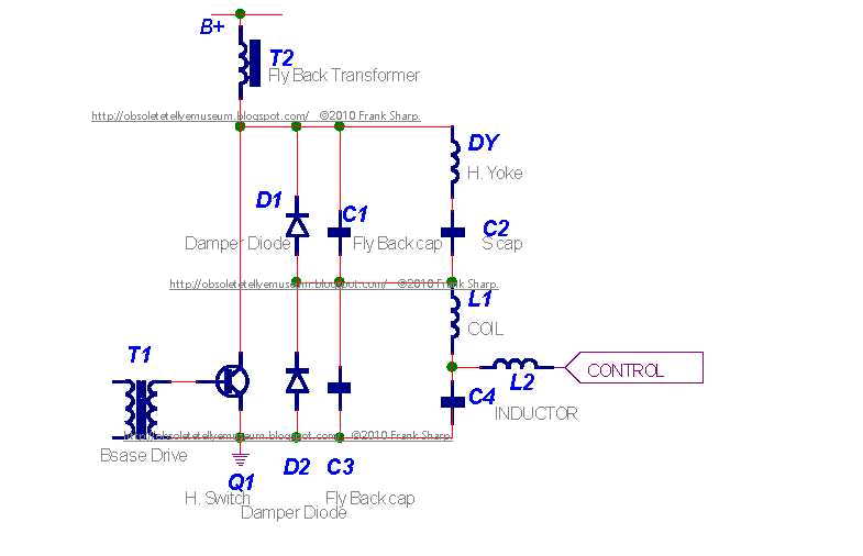 SPLIT DIODE MODULATOR
This horizontal circuit consists of two parts. D1, C1, C2 and DY are the components as described above.
D2, C3, C4 and L1 are a second “dummy” horizontal section that does not cause deflection current. By the
D.C. analyzing this circuit the voltage across C2 + C4 must equal the supply voltage (B+). Deflection
current in the DY is related to the supply voltage minus the voltage across C4. For a maximum horizontal
size the control point must be held at ground. This causes the dummy section to not operate and the DY
section will get full supply voltage. If the control point is at 1/3 supply then the DY section will be
operating at 2/3 supply.
Note: The impedance of (D1,C1,C2 and DY) and (D2,C3,C4 and L1) makes a voltage divider. If the
control point is not connected then there is some natural voltage on C4. Most split diode monitors are built
to pull power from the dummy section through L2 to ground. A single power transistor shunts from the
control point to ground. It is true that power can be supplied from some other supply through L2 to rise the voltage on C4. For maximum range a bi-directional power amplifier can drive the control point.
The most exciting feature if the split diode modulator is that the flyback pulse, as seen by the flyback
transformer, is the same size at all horizontal size settings.
HORIZONTAL SWITCH/DAMPER DIODEOn the right hand side of the screen, the H. switch transistor conducts current through the deflection yoke.
This current comes from the S correction capacitors, which have a charge equal to the effective supply
voltage. The damper diode allows current for the left hand side of the screen to flow back through the
deflection yoke to the S capacitors.
FLYBACK CAPACITOR
The flyback capacitor connects the hot side of the yoke to ground. This component determines the size and
length of the flyback pulse. ‘Tuning the flyback capacitor’ is done to match the timing of the flyback pulse
to the video blanking time of the video signal. The peak flyback voltage on the horizontal switch must be
set to less that 80% if the Vces specification. The two conditions of time and voltage can be set by three
variables (supply voltage, retrace capacitor and yoke inductance) .
S CAPACITOR
The S capacitors corrects outside versus center linearity in the horizontal scan. The voltage on the S cap
has a parabola plus the DC horizontal supply. Reducing the value of S cap increases this parabola thus
reducing the size of the outside characters and increasing the size of the center characters.
S Capacitor value: Too low: picture will be squashed towards edges.
Too high: picture will be stretched towards edges.
By simply putting a capacitor in series with each coil, the sawtooth waveform is
modified into a slightly sine-wave shape. This reduces the scanning speed near the
edges where the yoke is more sensitive. Generally the deflection angle of the electron
beam and the yoke current are closely related. The problem is the deflection angle
verses the distance of movement on the CRT screen does not have a linear effect.
BASE DRIVE CURRENTThe base drive resistor determines the amount of
base drive. If the transistor is over driven the Vsat
looks very good, but the current fall time is poor.
If the base current is too small the current fall time is very fast. The problem is that the transistor will have many volts across C-E when closed.
The best condition is found by placing the transistor in the heaviest load condition. Adjust the base resistor for the least power consumption then increase the base drive a small amount. This will slightly over drive the base.
LIST OF COMMON FAULTS / THROUBLESHOOTING FOR GRUNDIG CHASSIS CUC220:
Grundig CUC220 Dead - intermittent. R646 ( 270k ) on PSU.Grundig CUC220 Display - intermittent incorrect channel disp IC663 ( 5v reg )
Grundig CUC220 Excess col & brightness when heated OK when Txt pcb dis'd - left it this way
Grundig CUC220 Frame collapse. R2779 ( 18k ) o/c remove to check.
Grundig CUC220 Frame distortion. IC TDA1770 if used , D2761 ( SKE4G1/04 ) , R2761 ( 6.8ohm , .75W )
Grundig CUC220 Goes straight off at sw on odd characters in display - HT = 180v (109v) HT pot int
Grundig CUC220 Horizontal shaking. Tuner/IF dry joints , check the electrolytics with freezer
Grundig CUC220 INT START UP C631 100uF 40v , C633 220uF , C647 1uF , C642 100uF + R646 270k
Grundig CUC220 int start up TDA4600
Grundig CUC220 Interference at sides. IC TDA2595 sync/line osc IC.
Grundig CUC220 Lack of frame at bottom when cold. C2768 ( 100uf ) on deflection PCB.
Grundig CUC220 No pic at switch on - looks like its off tune C2221 ( 1uf 63v ) in tuner/if unit.
Grundig CUC220 No vision with raster and sound. T2533 , Adj control SB , R2536 , C2536 , D2536 , D2532
Grundig CUC220 Pulling/Rolling C2216/2221 1µ 63v in IF can by TDA5500 chip
Grundig CUC220 Shutdown - intermittent switching off. Dry R646 ( 270k ) , TDA4600 , replace HT pot R647 ( 2.5k )
Grundig CUC220 Standby - intermittent going into standby. Change R647 to ceramic.
Grundig CUC220 Standby- intermittent going into standby. IC663 ( 5v reg )
Grundig CUC220 Startup - switch on problems & hum. Relay contacts jammed o/c.
No comments:
Post a Comment
The most important thing to remember about the Comment Rules is this:
The determination of whether any comment is in compliance is at the sole discretion of this blog’s owner.
Comments on this blog may be blocked or deleted at any time.
Fair people are getting fair reply. Spam and useless crap and filthy comments / scrapers / observations goes all directly to My Private HELL without even appearing in public !!!
The fact that a comment is permitted in no way constitutes an endorsement of any view expressed, fact alleged, or link provided in that comment by the administrator of this site.
This means that there may be a delay between the submission and the eventual appearance of your comment.
Requiring blog comments to obey well-defined rules does not infringe on the free speech of commenters.
Resisting the tide of post-modernity may be difficult, but I will attempt it anyway.
Your choice.........Live or DIE.
That indeed is where your liberty lies.
Note: Only a member of this blog may post a comment.