


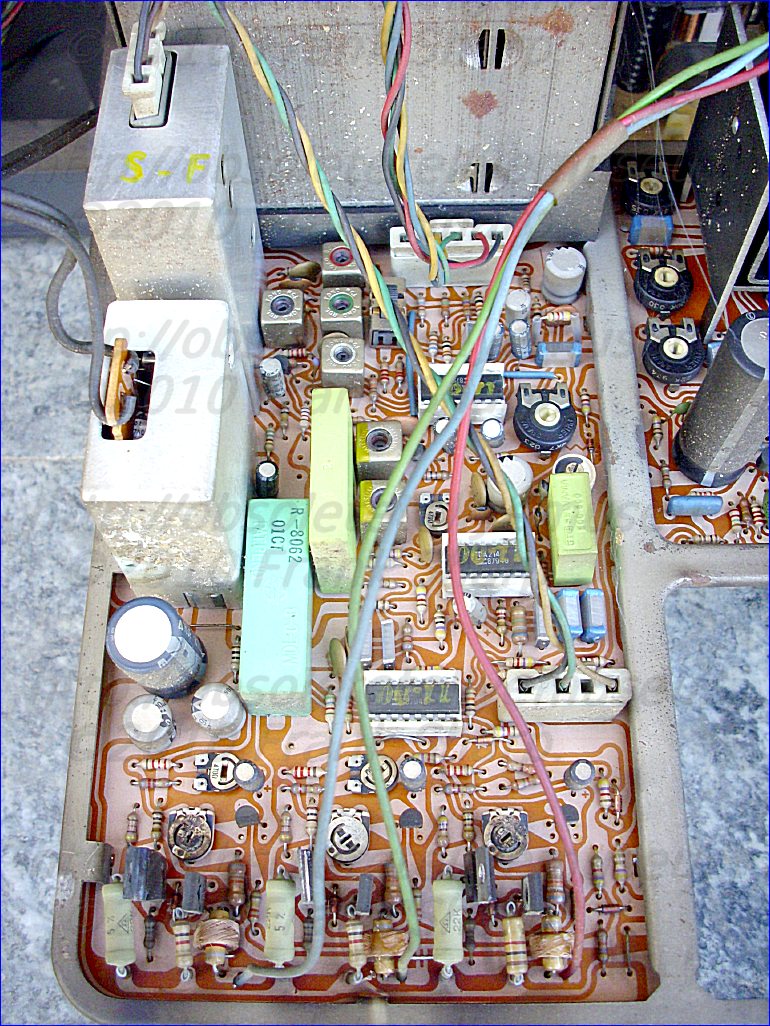


The MIVAR CHASSIS TV2018 + TV2036/1 + TV2039/2 was introducing the 30AX CRT TUBE BY PHILIPS and was replacing all previous models with THYRISTOR HORIZONTAL DEFLECTION TECHNOLOGY BASED CHASSIS TYPES WITH 20AX CRT TUBE.
AND It's the first MIVAR using a new tuning system replacing earlyer types based around ITT Chipset ASIC's but was anyway controlled by an ultrasonic remote system.
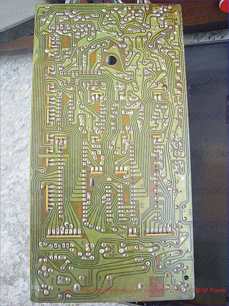
The T99 control box indeed is introducing first PLL FREQUENCY SYNTHESIZER IN MIVAR TV COLOR SET AND FIRST MIVAR TV SET CONTROLLED BY MICROCONTROLLER M3870.
On bottom floor part the st-by unit TV2320


The tuning control box MIVAR T99 is based around a SGS combination chipset:
M106A + M3870 + M120 + UAA1008P (MOTOROLA) MADE BY:
SGS is Società Generale Semiconduttori - Aquila Tubi E Semiconduttori (SGS-ATES, "Semiconductor General Society - Tubes and Semiconductors Aquila"), later SGS Microelettronica, a former Italian company now merged into STMicroelectronics
SGS Microelettronica and Thomson Semiconducteurs were both long-established semiconductor companies. SGS Microelettronica originated in 1972 from a previous merger of two companies:
- ATES (Aquila Tubi e Semiconduttori), a vacuum tube and semiconductor maker headquartered in the Abruzzese city of l'Aquila, who in 1961 changed its name into Azienda Tecnica ed Elettronica del Sud and relocated its manufacturing plant in the outskirts of the Sicilian city of Catania
- Società Generale Semiconduttori (founded in 1957 by Adriano Olivetti).
MIVAR (RADIOVAR) MOD 22" C804 T99 CHASSIS TV2018 + TV2036/1 + TV2039/2 PLL MICROCOMPUTER Frequency synthesizer tuning system for television receivers:
MOTOROLA UAA1008A-DP TUNING MEMORY SYSTEM LINEAR PROCESSOR CIRCUIT
The
UAA1008A provides the interfacing between the digital section of the
tuning memory system and the TV set. In addition, it supplies the
necessary functions and stabilized voltages for operating the complete
system.
When used in conjunction with the MC14425f29 and MC14426 it will perform the following:
• D/A conversion of varicap voltage
• 34 Volt regulation
• 5 volt regulation for supply of all VOO external lines
• Supply voltage supervisory control
• BAND decoding and driver (35 mAl
• TV station capture control with help of fly·back, video, and AFC signals.


" A method for tuning a television receiver having automatic frequency control to the carrier frequency of a selected broadcast channel with an associated channel number including generating a variable frequency signal by means of a local oscillator, generating a reference frequency signal by means of a reference oscillator, and generating a local oscillator correction signal for matching an intermediate frequency signal derived from said local oscillator signal and the carrier frequency signal with a predetermined nominal intermediate frequency signal, said method being characterized by the use of a microcomputer and comprising:
generating binary signals representing first and second digital tune words, said digital tune words representing a selected channel;
storing said first and second digital tune words in a first data memory in said microcomputer;
reading said first and second digital tune words from said first memory and generating a divided-down local oscillator frequency by the use of said first digital tune word and a divided-down reference oscillator frequency by the use of said second digital tune word;
comparing said divided-down local oscillator and reference frequencies and generating a control signal representative of the difference in frequency of said divided-down local oscillator and reference frequencies;
coupling said control signal to said local oscillator for causing it to be locked to the frequency of said received carrier signal;
mixing the local oscillator frequency signal and the carrier frequency signal to generate an intermediate frequency signal;
comparing said intermediate frequency signal with said predetermined nominal intermediate frequency signal and providing a tuning voltage to said microcomputer, said tuning voltage being indicative of the magnitude and direction of a tuning error between said intermediate frequency signal and said predetermined nominal intermediate frequency signal;
incrementally adjusting the reference oscillator frequency by means of a tuning signal provided to said reference oscillator by said microcomputer in response to said tuning voltage;
detecting when the incrementally changing, divided-down reference oscillator frequency causes the intermediate frequency signal to pass said predetermined nominal intermediate frequency signal; and
incrementally stepping the divided-down reference oscillator frequency back a predetermined number of steps following the passage of said predetermined nominal intermediate frequency signal by said intermediate frequency signal in tuning said television receiver to the selected channel.
"
1. A tuning system for the tuner of a television receiver capable of receiving a composite television signal and including frequency discriminator (AFT) circuit means, said system including in combination:
a reference oscillator providing a reference signal at a predetermined frequency;
a local oscillator in the tuner providing a variable output frequency in response to the application of a control signal thereto;
a programmable frequency divider means having first and second inputs coupled respectively to the output of said reference oscillator and said local oscillator for producing signals on first and second outputs having frequencies which are a programmable fraction of the frequency of the signals applied to the inputs thereto;
phase comparator means having one input coupled with the first output of said programmable frequency divider means and having another input coupled with the second output of said programmable frequency divider means for developing a control signal and applying such control signal to said local oscillator for controlling the output frequency thereof;
counter circuit means coupled with said programmable frequency divider means for initially setting said divider means to a predetermined division ratio and operating to change the programmable fraction of division thereof in accordance with changes in the count in said counter circuit means;
control circuit means coupled with the output of said frequency discriminator means and further coupled with said counter circuit means for causing said counter circuit means to count at a first rate in a predetermined direction determined by the state of the output signal from said discriminator means in the absence of a predetermined signal output from said frequency discriminator means until a predetermined maximum count is attained, thereupon resetting said counter circuit means to a count which is a predetermined amount less than said maximum predetermined count and continuing to count at said first rate in the same predetermined direction from said new count to continuously change the programmable fraction of said frequency divider means in accordance with the state of operation of said counter circuit means, said control means operating in response to said predetermined signal output from the frequency discriminator means for terminating operation of said counter circuit means; and
further means for terminating operation of said counter circuit means at said first rate and causing operation thereof at a second slower rate.
2. The combination according to claim 1 wherein said further means includes timing means initiated into operation simultaneously with the setting of said divider means to a predetermined division ratio, and after a predetermined time interval said timing means producing an output signal applied to said counter circuit means to cause operation thereof to take place at said second slower rate. 3. The combination according to claim 1 wherein said counter circuit means includes a reversible digital counter coupled with said programmable frequency divider, means and said control circuit means causes said counter circuit means to count in said predetermined direction when the output of said frequency discriminator is of a first state and to count in the opposite direction when the output of said frequency discriminator is of second state; and said further means comprises means coupled with the output of said frequency discriminator and with said counter circuit means to take place at said second slower rate in response to a predetermined number of changes of state of frequency discriminator. 4. The combination according to claim 3 further including means responsive to the selection of a new channel in said television receiver for resetting said further means to an initial condition of operation. 5. The combination according to claim 4 wherein said further means comprises a search termination counter means operative to provide an output signal applied to said counter circuit means in response to a count thereby of a predetermined number of changes of state of said frequency discriminator to cause said counter circuit means to be operated at said second slower rate.
Both of the above mentioned patents are directed to frequency synthesizer tuning systems for use with television receivers to enable operation of the receivers with minimal viewer fine tuning adjustments. By the utilization of the frequency synthesizer tuning systems of these patents, the fine tuning adjustment which is necessary with conventional types of television receiver tuning systems has been substantially eliminated. The system employed in the '953 patent permits utilization of a frequency synthesizer tuning system which correctly tunes to a desired television station or channel even if the transmitted signals from that station are not precisely maintained at the proper frequencies. The '535 patent is directed to a signal seek tuning system adaptation of the frequency synthesizer tuning system of the '953 patent which still permits implementation of all of the desired wide-band pull in range of the frequency synthesizer system of the '953 patent.
The systems of the foregoing patents operate effectively to correct automatically for frequency offsets in a frequency synthesizer tuning system without affecting the operation of the conventional frequency synthesizer used in the system. The systems of these patents are in widespread use commercially and permit direct selection, with automatic fine tuning adjustment, of any desired VHF channel which the viewer wishes to observe. In addition, the signal seek adaptation disclosed in the '535 patent couples all of the advantages of the frequency synthesizer tuning system of the '953 patent with the desirability of providing bidirectional signal seek operation.
While the systems disclosed in the foregoing patents operate in a highly satisfactory manner to accomplish the desired results of accurate tuning without the necessity of fine tuning adjustments, the circuitry for accomplishing the desired results is somewhat complex. It is desirable to reduce the circuit complexity and the number of signal detectors for accomplishing these results without compromising the accuracy of operation of the system.
SUMMARY OF THE INVENTION
Accordingly, it is an object of this invention to provide an improved tuning system for a television receiver.
It is an additional object of this invention to provide an improved frequency synthesizer tuning system for a television receiver.
It is another object of this invention to provide an improved frequency synthesizer tuning system for a television receiver which includes a provision for adjusting the synthesizer loop for frequency offsets in the received signal with a minimum number of signal detectors.
It is still another object of this invention to provide an improved frequency synthesizer tuning system for a television receiver which operates to adjust the synthesizer loop for frequency offsets in the received signal over a relatively wide pull in range in response to the output of the receiver frequency discriminator by changing the division ratio of a programmable frequency divider in the reference oscillator leg or local oscillator leg of the synthesizer loop at a first relatively high rate from an initial nominal value to a pre-established maximum in one direction, and then resetting the division ratio to a second nominal value once the maximum is reached and continuing to incrementally change the division ratio in the same direction from the second nominal value until a properly tuned condition is indicated by the output of the receiver AFT frequency discriminator, followed by control at a lower rate of operation to maintain tuning during transmitting station drifts.
In accordance with a preferred embodiment of this invention, the frequency synthesizer tuning system for a television receiver includes a stable reference oscillator and a voltage controlled local oscillator in the tuner. A programmable frequency divider is connected between the output of the reference oscillator and one input to a phase comparator, the other input of which is supplied by the output of the local oscillator. The output of the phase comparator then comprises a control signal which is supplied to the local oscillator to control the frequency of its operation.
A counter circuit is connected to the programmable frequency divider for initially setting the divider to a predetermined division ratio upon selection of a desired channel by the viewer. The counter then operates to change the programmable fraction of the division ratio at a first relatively high rate in a direction controlled by the output from the receiver picture carrier discriminator in the absence of a predetermined signal output derived from the discriminator. A control means causes the counter circuit to count in this direction until it is determined that a station is tuned or a predetermined maximum count is attained if no station is correctly tuned, thereupon resetting the counter circuit to a count which is a predetermined amount less than the maximum predetermined count. Counting is continued in the same predetermined direction from the new lesser count to continuously change the programmable fraction of the frequency divider in accordance with the state of operation of the counter.BRIEF DESCRIPTION OF THE DRAWINGS
FIG. 1 is a block diagram of a television receiver employing a preferred embodiment of the invention;
FIG. 2 is a detailed block diagram of a portion of the circuit of the preferred embodiment shown in FIG. 1;
FIG. 3 is a detailed circuit diagram of a portion of a circuit shown in FIG. 1;
FIG. 4 is a flow chart of the control sequence of operation of the circuit shown in FIG. 1 and 2; and
FIG. 5 shows a waveform and time/frequency chart, respectively, useful in explaining the operation of the circuit shown in FIGS. 1, 2 and 3.
DETAILED DESCRIPTION
Referring now to the drawings, the same reference numbers are used throughout the several figures to designate the same or similar components.
FIG. 1 is a block diagram of a television receiver, which may be a black and white or color television receiver. Mo
 st of the circuitry of this receiver is conventional, and for that reason it has not been shown in FIG. 1. Added to the conventional television receiver circuitry of FIG. 1, however, is a frequency synthesizer tuning system, in accordance with a preferred embodiment of the invention, which is capable of automatically changing the reference frequency when a frequency offset exists in the received signal for a particular channel.
 Transmitted composite television signals, either received over the air or distributed by means of a master antenna TV distribution system, are received by an antenna 10 or on antenna input terminals to the receiver. As is well known, these composite signals include picture and sound carrier components and synchronizing signal components, with the composite signal applied to an RF and tuner stage 11 of the receiver. The stage 11 includes the conventional RF amplifiers and tuner sections of the receiver, including a VHF oscillator section and a UHF oscillator section. Preferably, the UHF and VHF oscillators are voltage controlled oscillators, the freuency of operation of which are varied in response to a tuning voltage applied to them to effect the desired tuning of the receiver.
The output of the RF and tuner stages 11 is applied to the remainder of the television receiver 14, which includes the IF amplifier stages for supplying conventional picture (video) and sound IF signals to the video and sound processing stages of the receiver 14. The circuitry of the receiver 14 may be of any conventional type used to separate, amplify and otherwise process the signals for application to a cathode ray tube 16 and to a loudspeaker 17 which reproduce the picture and sound components, respectively, of the received signal.
The receiver 14 also includes a conventional AFT or automatic fine tuning discriminator circuit and additionally may include a synch separator circuit for producing an output in response to the presence of vertical synchronizatin pulses, a picture carrier detection circuit, and an automatic gain control (AGC) amplifier. Outputs representative of these sensor components are shown as being coupled over a group of lead 20 to sensory circuitry 22, which in turn couples outputs representative of the operation of these various sensor circuits to a microprocessor unit 23 for controlling the operation of the microprocessor unit.
The microprocessor unit 23 is utilized in the system of FIG. 1 for controlling the operation of a frequency synthesizer tuning system capable of automatic offset correction. When the viewer desires to select a new channel, he enters the desired channel number into a channel selection keyboard 25. There are a number of different keyboards which may be employed to accomplish this function, and the particular design is not important to this invention. The channel selector keyboard 25 also may include switches or keys for initiating a signal seek function in either the "up" or "down" direction.
Information represented by the selection of channel numbers on the keyboard 25 is supplied to the microprocessor unit 23 which provides output signals over a corresponding set of leads 27 to the tuners (local oscillators) 11 to effect the appropriate band switching control for the tuners 11 in accordance with the particular channel which has been selected. In addition, the keyboard 25, operating through the microprocessor unit 23, provides output signals which operate a channel number display 29 to provide an appropriate display of the selected channel number to the viewer.
In accordance with the time division multiplex operation of the microprocessor 23, the count of the programmable frequency divider 35 initially is adjusted to a fixed count by the application of appropriate output signals from the microprocessor unit 23 to a point selected to be at or near the mid-point of the operating range of the programmable frequency divider 35. Thus, the output of the divider 35 is a stable reference frequency (because the input is from the reference crystal oscillator 34) which is used to establish initially and to maintain tuning of the receiver to the selected channel.
The output of the programmable divider 35 is applied to one of two inputs of a phase comparator circuit 37. The other input to the phase comparator circuit 37 is supplied from the selected one of the VHF or UHF oscillators in the tuner stages 11 through the programmable frequency divider 31. The phase comparator circuit 37 operates in a conventional manner to supply a DC tuning control signal through a phase locked loop filter circuit 39 and over a lead 40 to the oscillators in the tuner system 11 to change and maintain their operating frequency.
With the exception of the use of the microprocessor unit 23, the operation of the system which has been described thus far is that of a relatively conventional frequency synthesizer system incorporated into a television receiver. This system is similar to the system of the '953 patent. As in the system of that patent, the system shown in FIG. 1, when the transmitted station or station received on a master antenna distribution system provides the station or channel signals at the proper frequency, operates as a relatively conventional frequency synthesizer system. If, however, there is a frequency offset in the received signal to cause the carrier of the received signal to be displaced from the frequency which it should have to some other frequency, it is possible that the system would give the appearance of mistuning to the received station. The microprocessor 23, operating in conjunction with the sensory circuitry 22, is employed in conjunction with the countdown or programmable frequency divider circuit 35 to eliminate this disadvantage and still retain the advantages of frequency synthesizer tuning.
Reference now should be made to FIG. 2 which shows details of t
 he interface between the keyboard 25, the microprocessor unit 23, and the circuitry used in the frequency synthesizer portions of the system. A commercially available microprocessor which has been used for the microprocessor 23, and which forms the basis for the diagramatic representation of the microprocessor in FIG. 2, is the Matsushita Electronics Corporation MN1402 four-bit single-chip microcomputer. This microcomputer has two, four-bit parallel input ports labeled "A" and "B". In addition, three output ports, a five-bit output port "C" and two four-bit output ports "D" and "E" are provided. The internal configuration of the microcomputer 23 includes an arithmetic logic unit (ALU), a read only memory (ROM) for storing instructions and constants, and a random access memory (RAM) used for data memory, arranged into four files, each file containing 16 four-bit words. These words are selected by X and Y registers and this memory is used, for example, for timers, counters, etc., and also is used to hold intermediate results. To facilitate an understanding of the operation of the system, a portion of this memory is shown in FIG. 2 as a clock 81 and a reversible counter 82 connected between the "B" input port and the "D" output port. The microcomputer 23 is programmed to permit it to operate in conjunction with the remainder of the circuits shown in FIG. 2. The programming techniques are standard, and the microcomputer 23 itself is a standard commercially available circuit component.
 There are several system parameters that must be selected in the operation of the system shown in FIG. 2. The selection of the nominal frequency of the two signals that feed the phase comparator circuit 37 is an example. Channel selection is provided by changing the frequency division ratio of the selector counter 31 which divides the local oscillator signal after this signal is passed through a prescaler circuit 32 and a divide-by-two divider circuit 41. The nominal frequency from the programmable frequency divider 31 (selector counter) is selected so that the local oscillator (tuner) 11 can be set exactly on frequency for all channels.
A compromise solution which is utilized in the circuit of FIG. 2 is to cause the frequency division chain from the local oscillator 11 in the tuner to the phase comparator 37 to be composed of the fixed divide-by-256 prescaler 32, and a fixed divide-by-4 division, which is accomplished by the divider 41 at the input of the counter 31 and a second divider 42 at the output of the counter 31. The variable frequency divider counter 31 then is loaded by means of three latch circuits 44, 45 and 46 at an appropriate time by the time division multiplex operation of the microcomputer 23 and a number that programs the programmable frequency divider counter 31 to divide by the numerical value of the frequency of the local oscillator in MHz for the channel selected. For example, if the receiver is to be tuned to channel 2, which has a nominal local oscillator frequency of 101 MHz, the programmable frequency divider 31 is set to divide by 101. If the receiver is to be tuned to channel 83, which has a nominal local oscillator frequency of 931 MHz, the programmable frequency divider 31 is set to divide by 931. In both cases, the variable divider 31 produces a 1 MHz signal. However, because of the fixed divide-by-256 and the two fixed divide-by-two dividers in series with the programmable divider 31, an output frequency of 976.5625 Hz is supplied from the output of the divider 42 to the upper input of the phase comparator 37.
Although the D output ports of the microcomputer 23 are connected in common to all of these various portions of the circuit, the selection of which of the latches are enabled to respond to the particular output signals appearing on the D output ports at any given time is effected through the C and E output ports of the microcomputer 23 in a time division multiplex fashion. A decoder circuit 52, connected to the lowermost three outputs of the E output port of the microcomputer 23, is used to apply unique decoding signals at different times in the time division multiplex sequence of operation of the microcomputer 23 to the five latch circuits 44, 45, 46, 49 and 50, respectively. At any given time in the sequence, only one of these latch circuits is enabled for operation. A latch load signal is applied from the upper output (EO3) at each cycle of operation of the signals appearing on the E output port to set the latch circuit which is enabled by the output of the decoding circuit 52 with the data appearing on the other inputs to the latch circuit. This data simultaneously appears on the four outputs of the D output port of the microcomputer 23.
Thus, in rapid sequence, the latch circuits 44, 45 and 46 are set to store the division number corresponding to the selected channel entered onto the keyboard 25, and the latch circuits 49 and 50 are each operated to set the programmable divider reference counter 35 to a center or nominal count, which is always the same upon the selection of a new channel on the keyboard 25. Similarly, the two right-hand outputs of the C output port (CO6 and CO5) enter the two digits of the selected channel number in the drivers of the display circuit 29 at the proper time in the binary encoded sequence when these digits appear on the four-bit binary encoded representation of the D output port. This results in a visual display of the channel number selected.
In addition to the selection of a channel number directly by the keyboard 25, the keyboard also may include an additional switch 56, which is scanned in the time division multiplex sequence to determine if the receiver is placed in a "seek" mode of operation (when the signal seek capability is incorporated into such a receiver). Operating in conjunction with the signal seek switch 56 are a pair of "up" and "down" seek direction input switches shown with a graphic representation of the seek directions on the keyboard 25. A further provision is provided by two keys labeled "U" and "D", which are used for "manual" fine tuning of the receiver in the "up" or "down" directions depending upon which of the two keys U or D has been operated. The keyboard 25 includes one additional switch 58 which may be used to disable the automatic fine tuning (AFT) portion of the circuit by rendering the microcomputer insensitive to the signal output from the AFT circuit, in a manner described more fully subsequently.
As is apparent from the foregoing, the microcomputer 23 provides the intelligence, decision making, and control for the system operation. It is a complete self contained computer. The decisions or signal inputs upon which the microcomputer 23 bases its operation include, in addition to the inputs from the keyboard 25, inputs on sensory inputs into the B input port and into the SNS1 and SNS0 inputs as shown in FIG. 2. These input signals are used to provide an indication to the microcomputer 23 of the presence or absence of a received signal; and if the presence of such a signal is indicated, the inputs provide a further indication of the accuracy of the tuning of the receiver to that signal. If the system is being operated solely in a manual mode of operation (AFT switch 58 open), the microcomputer 23 disregards all of this sensory information and tunes to the frequency allocation of the channel selected in the manner described above. The system will stay tuned to this condition, operating as a conventional frequency synthesizer, whether or not a station is present in the received signal.
When the system is placed in its automatic mode of operation (similar to the mode of operation of the above mentioned '953 patent), the counter 82, integrally formed as part of the microcomputer 23, continuously adds or subtracts one number at a time from the nominal value or programmable division fraction entered into the programmable frequency divider 35 at the outset of each new channel number selection when frequency offset (mistuning) is present. The counter 82 is driven at a relatively high counting rate by clock pulses from the clock 81 during this initial or forced search mode of operation. Thus, automatic offset correction is provided for any channel which is off its assigned frequency. The offset correction automatically adjusts the frequency of the local oscillator by changing the division ratio of the signal from the reference oscillator 35 applied to the lower input of the phase comparator 37. By doing this, the output of the phase comparator 37 applied to the local oscillator 11 varies to cause the oscillator to be tuned in the proper direction to compensate for the transmitting station mistuning. When the system is operating in its automatic mode of operation, the microcomputer 23 responds to the sensor information applied to it on its B input ports and on the S1 input port shown in FIG. 2. These inputs are obtained from the various outputs of the operational amplifiers shown connected to the corresponding input ports in the detailed circuit of FIG. 3. Depending upon whether the receiver is provided with a signal seek feature or not, one or more of the sensory inputs of the circuit of FIG. 3 are used. The s
 ystem shown in the drawings has a capability of correcting for frequency offsets larger than 1.5 MHz on channels 2 and 7 and approximately 2 MHz on channels 6 and 13. The remainder of the channels have a range between these two values.
 If the receiver is not tuned properly, the micromputer 23 executes the localized search of the tuning range mentioned above. Since there is a necessary settling down time for the tuning of a television receiver immediately following selection of a new channel, a time interval of 250 milliseconds has been selected to prevent any localized search or offset frequency correction until the expiration of this "settling down" time period. If, at the end of this 250 millisecond time interval, a properly tuned station is present, this is indicated by the sensory outputs from the television receiver and no localized search is effected to change the division ratio or programmable divider count in the reference counter 35 for a system that also has signal seek.
A system with no signal seek capability is described later that requires less sensory input but which uses a time period where a forced search is required directly after the settling time interval.
The lower graph of FIG. 5 plots the relative frequency of the local oscillator 11 to the received signal frequency with respect to time. The various arrows are used to indicate the manner of operation of the counter 82 in the microcomputer 23 in conjunction with the reference counter 35 for adjusting for any mistuning conditions which may exist after the initial station selection has been effected in the manner described above.
If the receiver is properly tuned, the outputs from the comparators 62 and 63 of FIG. 3 which are combined together and applied to the input port B11 of the microcomputer 23, provide an indication that the tuning is within the properly tuned center frequency window. As a consequence, no further operation of the microcomputer to change any of the outputs applied to the latch circuits 49 and 50 for the duration of this condition is effected. On the other hand, if the receiver is mistuned on either side of the proper tuning frequency, the various operating characteristics shown in FIG. 5 are effected.
Assume initially that the receiver is capable of making tuning adjustments over a range of fc plus Δf to fc minus Δf, as indicated in the top waveform of FIG. 5. Three specific examples of mistuning will then be considered. Initially, assume that the local oscillator is mistuned relative to the received signal to a frequency f1 as shown in the lower graph of FIG. 5. In this condition, the outout of the frequency discriminator 60 is positive since this signal frequency lies to the lefthand side of the center or properly tuned region of operation of the discriminator. Under this condition of the operation, the input signal applied to the sensor port B12 of the microcomputer 23 is such that the microcomputer counter 82 is caused to advance in a positive direction to change the programmable division ratio or count of the reference counter 35 in a manner to force the output of the phase comparator 37 to adjust the frequency of the local oscillator until the proper tuning indicated at point B in the lower graph of FIG. 5 is reached. The time interval for accomplishing this result is measured from the upper end of the arrow representative of the frequency f1 to the point B.
Now assume that the receiver mistuning is to a frequency f2 which as shown in FIG. 5 as located on the righthand-side of the center axis fc. In this condition, the discriminator output is negative. This is reflected in the output of the comparator 61 applied to the input port B12 of the microcomputer 23. The polarity of this signal is identified by the microcomputer 23 to cause the counter 82 in it to operate in the reverse direction. As this count is applied on a step-by-step basis through the latch circuits 49 and 50 to the reference counter 35, the division ratio or count of the reference counter (divider) 35 is changed. As a result, the reference oscillator signal applied to the phase comparator 37 causes the phase comparator 37 output to drive the local oscillator frequency in a direction opposite to that considered in the first example. This is shown by the vector interconnecting the top of the arrow representative of f2 to point A on the time/frequency graph of FIG. 5.
As discussed in the general discussion above, whenever the tuning frequency reaches the narrow window on either side of fc, the outputs of the comparators 62 and 63 provide the necessary indication on the sensory input port terminal B11 to cause termination of the operation of the counter 82 in the microcomputer 23. Then the reference counter 35 remains set to the count attained just prior to the appearance of this input signal on the input port B11 of the microcomputer 23.
A third mistuning condition can exist, and ordinarily this condition results in an ambiguity which cannot be corrected simply by responding to the signal polarity at the output of the frequency discriminator. This is indicated by the mistuned condition where the difference between the local oscillator frequency f3 and the transmitter frequency is such that the signal f3 lies in the range to the right of the negative portion of the discriminator output shown in the upper waveform of FIG. 5. In this condition, the associated sound causes the discriminator output to be positive; so that the television receiver normally would attempt to tune toward the next adjacent channel and away from the properly tuned center frequency of the channel which is desired. The output of the discriminator 60 in this situation is the same as it was in th
 e first example considered for frequency f1; so that the counter 82 of the microprocessor 23 operates to change the count in the reference counter 35 in a manner to cause the local oscillator frequency to go higher toward a frequency f3 +Δf, as shown in FIG. 5.
 A predetermined number of counts of the counter 82 in the microcomputer 23 are necessary for the microcomputer to count through the frequency range Δf, and this range is selected to be within the pull in or operating range of the system. Once this count has been attained, the microcomputer counter 82 immediately is reset back to a count which corresponds to a frequency 2 Δf lower than the frequency attained by the maximum count. This is indicated in FIG. 5 by the frequency f3-Δf. Because the microcomputer counter 82 is limited to counting a number of counts equal to Δf, this new frequency now is on the lefthand side of the center line fc, shown in both waveforms of FIG. 5. This places the local oscillator frequency at a point such that the frequency discriminator output is the positive output shown on the lefthand-side of the upper waveform of FIG. 5. Counting continues in the same direction as previously. This time, however, it is in a proper direction to bring about correct tuning; and when the center frequency is reached, the output of the comparators 62 and 63 cause the microcomputer 23 to stop its count. The proper tuning point attained is indicated at point C on the graph of the lower part of FIG. 5.
When the channel once again is changed by operation of the keys in the keyboard 25 or operation of the channel selection circuitry from a remote control unit, this new channel input is sensed by the microcomputer 23 from the signals applied to the A input port and the clock 81 is reset to its fast time or the forced search mode of operation; and the process resumes.
Instead of employing an additional decoding function in the decoder 52, a separate decoder also could be connected to the outputs of the D output ports to feed back the signal to the B13 input terminal of the B input port of the microcomputer 23. The operation of the system to change the rate or frequency of the pulses applied by the clock 81 to the counter 82 otherwise is the same as described above.
Although applicant has found that it is preferable to correct for mistuning or frequency offsets by adjusting the count or division ratio of the counter 35, such offset adjustments also could be effected by adjusting the count in the counter 31 in the local oscillator signal line. The operation in such a case is the same as described above for adjusting the count in the counter 35.
If the receiver is to be used with an automatic signal seek mode of operation, however, additional sensory inputs are necessary. These inputs operate in conjunction with the output of the frequency discriminator 60. The operation of the microcomputer 23 in controlling the count of the reference programmable frequency counter divider 35 is the same as described above. The additional sensory inputs simply are used in conjunction with the outputs of the comparators 62 and 63 to signal the microcomputer 23 to assure that tuning is to a picture channel rather than an adjacent sound channel. This is accomplished by utilizing the output of the synchronizing signal separator 65 which is applied to a comparator 67 to produce an output signal to the SNS1 sensory input of the microcomputer 23 only when vertical synchronizing signal components are present.
In addition, the output of a picture carrier detector 69 is applied to the input of a comparator 70 to produce an output to the B10 sensory input of the microcomputer 23. If the picture carrier detector 69 is producing an output indicative of the presence of a carrier, but no output is being obtained from the vertical synch separator 65 at the same time, the system is mistuned to a sound carrier and the microcomputer 23 is permitted to continue its localized search until a properly tuned station is found. Only when there is coincidence of signals from the picture carrier detector 69, the synch signal separator 65, and the automatic frequency discriminator window as determined by the comparators 62 and 63, is the microcomputer operation terminated to indicate that a properly tuned channel is present.
Further insurance of tuning the receiver only to a strong signal also can be provided by the addition of an AGC amplifier 72. This is connected to a comparator 74 coupled to the B10 input port along with the output of the picture carrier detector comparator 70. When the AGC amplifier 72 is used as a sensory input, the microcomputer operation, when the system is used in a signal seek mode, is only terminated to indicate reception of a valid signal when that signal is strong enough to produce the desired output from the comparator 74. The signal level which is acceptable is set by a potentiometer 75.
It should be noted that when the system is operated in a signal seek mode, the sensory inputs must indicate the reception of a properly tuned signal within a pre-established time period. If no signal is sensed by the various sensory input circuits operating in conjunction with one another as described above, the microcomputer 23 automatically steps to the next channel number and repeats the sequence of operation described above. This is when it is placed in its signal seek mode of operation. If signal seek is not employed, the additional sensory circuits 65, 69 and 72 are not necessary, and the inputs to the microcomputer which are provided from these sensory circuits are not utilized. The sensory signal input which is used both for a receiver without a signal seek capability of operation and for a receiver which has a signal seek mode of operation in it, is the output of the frequency discriminator 60 operating in conjunction with the comparators 61, 62 and 63 as described above.
As indicated above, the wideband method of tuning precisely to an incoming signal that is at the wrong frequency described here only needs the frequency discriminator sensory information. The method that uses the additional sensors described above is needed to make this system operate compatibly with signal seek but it is not restricted to seek operation.
The fast time or forced search operation of the system can be terminated in a different way other than the preestablished time-out period described above in conjunction with the operation of the circuit shown in FIG. 2. Generally, it is desirable to build into the system (or program into the system by means of software) such a maximum time-out period to effect the operation which has been described above to terminate the search and cause the clock 81 thereafter to operate in a low speed mode of operation. Termination also can be accomplished by sensing the number of changes in the direction sensor input applied to the B12 terminal of the B input port to cause the search to be terminated when this direction changes three times (or more). By doing this, any flicker that might be observed on the screen of the television receiver is minimized, since the forced search still takes place at the high rate of application of clock pulses from the clock 81 to the counter 82 in the same manner described above.
Termination of the search, however, also may be effected by means of a search terminate counter 78 (FIG. 3), which is advanced by pulses applied to it each time the output of the comparator 61 changes its sign (indicative of a change in direction for the counter 82) as applied to it through the B12 input port, as described earlier. After three of these changes, or some other number if desired, an output pulse is obtained from the search terminate counter 78 and is applied to the SNS0 input of the microcomputer 23. This causes the operation of the clock 81 to be switched to its low speed mode of operation to terminate the fast or "forced search" mode of operation. The next time a new channel number is entered on the keyboard 25, a reset pulse is applied to the search terminate counter 78 to reset it to its original or zero count, thereby readying it for another sequence of operation. It is apparent that the search terminate counter 78 may not always be operated to terminate the count, since the time-out interval which is sensed by the decode circuit 52 and applied to the B13 input port of the microcomputer 23 may occur before there are three changes of direction of the search. In any event, the next time a new channel number is entered into the keyboard 25, the search terminate counter 78 is reset; so that it is irrelevant whether this counter reaches a full count or not to effect the termination of the forced search operation of the system.
FIG. 4 shows the control sequence of the system which is stored in the ROM (Read Only Memory) of the microcomputer 23. The microcomputer 23 operates by always running through the flow sequence, via loops L1, L2 and L3. Loop L1 corresponds to a new channel selection by two digit number entry. Loop L2 corresponds to channel number increment or decrement by an up or down key operation, respectively, or by seek operation. Loop L3 corresponds to fine tuning, either manual or automatic. To obtain exact timing for system control, the microcomputer 23 receives a standard timing pulse from the output of the reference counter 35 divided in a divide-by-five counter 80 and applied to the A13 input port of the microcomputer 23. The control functions which are programmed into the microcomputer 23, as indicated in the flow chart of FIG. 4, are outlined in the following paragraphs.
Channel Number Correction: An invalid two digit channel number entry (0, 1, 84, 99) is corrected. When the operation of the receiver is in the signal seek mode, the next channel up from 83 is channel 2, and the next lower channel from channel 2 is 83. PLL Control I: For a given channel number, a corresponding binary code for the PLL selector counter 31 is derived as described previously. For UHF channels, the local oscillator frequency separation between two adjacent channels is 6 MHz and the code for PLL is generated by the microcomputer 23 through means of a simple calculation. This code then is transferred from the microcomputer 23 to the latches 44, 45 and 46 as described previously.
PLL Control II: This routine of the microcomputer 23 is used to transfer the fine tuning data to the latches 49 and 50 which control the count of the reference counter 35 in the PLL circuit.
Channel Number Display: The channel number is transferred from the microcomputer 23 to the driver latches of the display driver circuit 29.
Key Input Detection: The keyboard is arranged as the matrix circuit shown in FIG. 2. ROM programming for scanning and acknowledging a keyboard entry only after successive indications provides protection against false entry due to contact bounce. The four data output lines of the D output port of the microcomputer 23 are used to transfer data to the phase lock loop section of the circuit and to the display circuit 29, as well as for scanning the keyboard matrix circuit.
Time Count: The microcomputer 23 receives a basic timing pulse of approximately 200 Hz from the output of the divider 80 and performs various controls for each timing pulse. By way of example, sensing for the vertical synch input (when the system is used with a signal seek capability) on the input port SNS1 takes place every 2.5 milliseconds. Automatic seek timing is selected to be 133 milliseconds for UHF channels. All of these timing pulses are derived from the basic synchronization timing pulse applied to the microcomputer on the A13 input port from the output of the divider 80. Various other timing values used in the microcomputer to properly time multiplex sequence the operation are derived from this basic timing pulse.
Sensor Input Detection: As described previously, the output of the comparators shown in FIG. 3 reflect the status of the tuning of the television receiver. If no signal seek mode of operation is used, only the frequency discriminator or AFT discriminator 60 is necessary. When a system is being used in a signal seek mode, a proper television signal receipt is indicated by the presence of a vertical synch signal at the output of the synch signal separator 65 and corresponding outputs are applied to the input leads B10 and B11 (high level input signals) indicative of tuning to the "correct tuned" frequency discriminator window and reception of a picture carrier. As stated previously, the signal present on the B12 input lead is used to determine the direction of tuning when the receiver is operated in its automatic mode.
Mode Detection: The status of the seek and automatic/manual (A/M) switches are detected. If the A/M switch (not shown) is in its automatic position, automatic seek and offset correction are active. If only the seek switch is on, only seek is performed. If the A/M switch is in manual, manual fine tuning (MFT) is active.
Automatic Mode: If the TV receiver is not properly tuned for VHF channels in automatic, the local oscillator frequency is shifted automatically toward proper tuning. The fine tuning data is generated in the microcomputer 23 and is transferred to the latches 49 and 50 for the reference counter 35 in the PLL circuit.
Manual Fine Tuning (MFT) Control: The local oscillator frequency is shifted by pushing the fine tuning up (U) or down (D) pushbutton or switch. This MFT control can be applied to VHF channels as well as to UHF channels.
Channel Up/Down: When a channel up (upward pointing arrow) or down (downward pointing arrow) key closure in the keyboard 25 is detected, or upon a direct access to an unused channel, this routine is activated and the system will advance to the next channel in the selected direction.
The foregoing embodiment of the invention which has been described above and which is illustrated in the drawings is to be considered illustrative of the invention, which is not limited to the specific embodiment selected for this purpose. For example, hard-wired logic could be used to achieve the various circuit operations which are accomplished by the microcomputer 23 in conjunction with the other portions of the system. The relative ease of programming and debugging the microcomputer 23, however, make it much simpler to implement the system operation with the microcomputer than with hard-wired logic. With respect to the sensor circuit inputs to the system, an added degree of operating assurance can be provided by the addition of a sound carrier sensor in addition to the picture carrier sensor shown in FIG. 3. If this feature is desired, the output of the comparator for the sound carrier is combined with the outputs of the comparators 70 and 74 at the input terminal B10 of the B input port of the microcomputer 23. Because of the manner of the circut operation which has been described previously, however, the addition of a sound carrier detector to the system is not considered necessary, even for a system operating in the signal seek mode of operation. This is in contrast to conventional television receivers having a signal seek operation, in which detection of the sound carrier generally is a necessity to insure that mistuning of the receiver to an adjacent sound carrier does not take place. CIRCUITS DESCRIPTIONS:
- Luminance + chrominance + RGB Amplifiers
(TDA2151 + TDA2140 + TDA2161) (all FAIRCHILD)
DA1180P TV HORIZONTAL PROCESSOR
DESCRIPTION
The TDA1180P is a horizontal processor circuit for
b.w. and colour monitors. It is a monolithic integrated
circuit encapsulated in 16-lead dual in-line
plastic package.
APPLICATION INFORMATIONPin 1 - Positive supply
The operating supply voltage of the device ranges
from 10V to 13.2V
Pin 2 and 3 - Output
The outputs of TDA1180P are suitable for driving
transistor output stages, they deliver positive pulse
at Pin 3 and negative pulse at Pin 2.
The negative pulse is used for direct driving of the
output stage, while positive pulse is useful when a
driver stage is required.
The rise and fall times of the output pulses are
about 150 ns so that interference due to radiation
are avoided.
Furthermore the output stages are internally protected
against short circuit.
Pin 4 - Protection circuit input
By connecting Pin 4 of the IC to earth the output
pulses at Pin 2 and 3 are shut off ; this function has
been introduced to produced to protect the final
stages from overloads.
The same pulses are also shut off when the supply
voltage falls below 4V.
Pin 5 - Phase shifter filter
To compensate for the delay introduced by the line
final stages, the flyback pulses to Pin 6 and the
oscillator waveform are compared in the oscillatorflyback
pulse phase comparator.
The result of the comparison is a control current
which, after it has been filtered by the external
capacitor connected to Pin 5, is sent to a phase
shifter which adequately regulates the phase of the
output pulses.
The maximum phase shift allowed is: td = tp - tf
where tf is the flyback pulse duration.
Pin 5 has high input and output resistance (current
generator).
Pin 6 - Flyback input
The flyback pulse drives the high impedance input
through a resistor in order to limit the input current
to suitable maximum values.
The flyback input pulses are processed by a double
threshold circuit; this generates the blanking pulses
by sensing low level flyback voltage and the pulses
to drive the phase comparator by sensing high level
flyback voltage, therefore phase jitter caused by
ringing normally associated with the flyback pulse,
is avoided.
Pin 7 - Key and blanking pulse output
The key pulse for taking out the burst from the
chrominance signal is generated from the oscillator
ramp and has therefore a fixed phase position with
respect to the sync.
The key pulse is then added internally to the blanking
pulse obtained by correctly forming the flyback
pulse present at Pin 6.
The sum of the two signals (sandcastle pulse) is
available on low impedance at output Pin 7.
Pin 8 and 9 - Sync separators inputs
The video signal is applied by means of two distinct
biasing networks to pins 8 and 9 of the IC and
therefore to the respective vertical and horizontal
sync separators.
The latter take the sync pulses out of the video
signal and make them available to the rest of the
circuit for further processing.
Pin 10 - Vertical sync output
The vertical sync pulse, obtained by internal integration
of the synchronizing signal, is available at
this pin.
The output i
mpedance is typically 10kW and thelowest amplitude without load is 11V.
Pin 11 - Coincidence detector
From the oscillator waveform a gate pulse 7 ms
wide is taken whose phase position is centered on
the horizontal synchronism.
The gate pulse not only controls a logic block which
permits the sync to reach the oscillator-sync phase
comparator only for as long as its duration, but also
allows the latching and de-latching conditions of
the oscillator to be established.This function is
obtained by a coincidence detector which compares
the phase of the gate pulses with that of the
sync.
When the two signals are not accurately aligned in
time it means that the oscillator is not synchronized.
In this case the detector acts on the logic block to
eliminate its filtering effect and on the time constant
switching block to establish a high impedance on
Pin 12 (small time constant of low-pass filter).
This latter block also acts on the oscillator-sync
phase detector to increase its sensitivity and with it
the loop gain of the synchronizing system.
In this conditions the phase lock has low noise
immunity (wide equivalent noise bandwidth) and
rapid pull-in time which allows fairly short synchronization
times.
Once locking has taken place the coincidence detector
enables the logic block, causes a low impedance
on Pin 12 and reduces the sensitivity of the
phase comparator.
In these conditions the phase lock has high noise
immunity ( narrow equivalent noise bandwidth) due
to the complete elimination of interference which
occurs during the scanning period and the greater
inertia with which the oscillator can change its
frequency.
To optimize the behaviour of the IC if a video
recorder is used, the state of the detector can be
forced by connecting Pin 11 to earth or to + VS. The
characteristics of the phase lock thus correspond
to the lack of synchronization.
Pin 12 - Time constant switch, (see Pin 11)
Pin 13 - Control current output
The oscillator is synchronized by comparing the
phase of its waveform with that of the sync pulses
in the oscillator-sync phase comparator and sending
its output current I13 (proportional to the phase
difference between the two signals) to Pin 15 of the
oscillator after it has been filtered properly with an
external low-pass circuit.
The time constant of the filter can be switched
between two values according to the impedance
presented by Pin 12.
The voltage limiter at the output of the phase
comparator limits the voltage excursion on Pin 13
and therefore the frequency range in which the
oscillator remains held-in.
The output resistance of Pin 13 is:
l low when V13 > 4.3 or V13 < 1.6V
l high when 1.6V < V13 < 4.3V
To prevent the vertical sync from reaching the
oscillator-sync phase comparator along with the
horizontal sync,a signal which inhibits the phase
detector during the vertical interval is taken from
the vertical output stage; inhibition remain even if
the video signal is not present.
The free running frequenc of the oscillator is determined
by the values of the capacitor and of the
resistor connected to Pins 14 and 15 respectively.
To generate the line frequency output pulses, two
theresholds are fixed along the fall ramp of the
triangular waveform of the oscillator.
Pin14 - Oscillator (see Pin 13)
Pin 15 - Oscillator control current input (see
Pin 13)
Pin 16 - Ground
TDA2541 IF AMPLIFIER WITH DEMODULATOR AND AFC

.SUPPLYVOLTAGE : 12V TYP .SUPPLYCURRENT : 50mATYP .I.F. INPUT VOLTAGE SENSITIVITY AT
F = 38.9MHz : 85mVRMS TYP .VIDEO OUTPUT VOLTAGE (white at 10% of
top synchro) : 2.7VPP TYP .I.F. VOLTAGE GAIN CONTROL RANGE :
64dB TYP .SIGNAL TO NOISE RATIO AT VI = 10mV :
58dB TYP .A.F.C. OUTPUT VOLTAGE SWING FOR
Df = 100kHz : 10V TYP
DESCRIPTION
The TDA2540 and 2541 are IF amplifier and A.M.
demodulator circuits for colour and black and white
television receivers using PNP or NPN tuners. They
are intended for reception of negative or positive
modulation CCIR standard.
They incorporate the following functions : .Gain controlled amplifier .Synchronous demodulator .White spot inverter .Video preamplifier with noise protection .Switchable AFC .AGC with noise gating .Tuner AGC output (NPN tuner for 2540)-(PNP
tuner for 2541) .VCR switch for video output inhibition (VCR
play back).
TDA2652A Vertical deflection circuit
DESCRIPTION
The TDA2652A is a monolithic integrated circuit for vertical deflection in large screen colour television receivers.
The circuit incorporates the following functions:
· Oscillator; switch capability for 50 Hz/60 Hz operation
· Synchronization circuit
· Blanking puls
e generator with guard circuit· Sawtooth generator with buffer stage
· Preamplifier with fed-out inputs
· Output stage with thermal and short-circuit protection
· Flyback generator
· Voltage stabilizers.
APPLICATION INFORMATION
The function is described against the corresponding pin number
1, 13. Oscillator
The oscillator frequency is determined by a potentiometer at pin 1 and a capacitor at pin 13.
2. Sync input/blanking output
Combination of sync input and blanking output. The oscillator has to be synchronized by a positive-going
pulse between 1 and 12 V. The integrated frequency detector delivers a switching level at pin 12.
The blanking pulse amplitude is 20 V with a load of 1 mA.
3. Sawtooth generator output
The sawtooth signal is fed via a buffer stage to pin 3. It delivers the signal which is used for linearity control,
and drive of the preamplifier. The sawtooth is applied via a shaping network to pin 11 (linearity) and via a
resistor to pin 4 (preamplifier).
4. Preamplifier input
The DC voltage is proportional to the output voltage (DC feedback). The AC voltage is proportional to the
sum of the buffered sawtooth voltage at pin 3 and the voltage, with opposite polarity, at the feedback
resistor (AC feedback).
5. Positive supply of output stage
This supply is obtained from the flyback generator. An electrolytic capacitor between pins 7 and 5, and a
diode between pins 5 and 9 have to be connected for proper operation of the flyback generator.
6. Output of class-B power stage
The vertical deflection coil is connected to this pin, via a series connection of a coupling capacitor and a
feedback resistor, to ground.
7. Flyback generator output
An electrolytic capacitor has to be connected between pins 7 and 5 to complete the flyback generator.
8. Negative supply (ground)
Negative supply of output stage and small signal part.
9. Positive supply
The supply voltage at this pin is used to supply the flyback generator, voltage stabilizer, blanking pulse
generator and buffer stage.
10. Reference voltage of preamplifier
External adjustment and decoupling of reference voltage of the preamplifier.
11. Sawtooth capacitor
This sawtooth capacitor has been split to realize linearity control.
12. 50 Hz/60 Hz switching level
This pin delivers a LOW voltage level for 50 Hz and a HIGH voltage level for 60 Hz. The amplitudes of the
sawtooth signals can be made equal for 50 Hz and 60 Hz with these levels.
MIVAR POWER SUPPLY COMBINED WITH BU208A TRANSISTOR HORIZONTAL DEFLECTION CIRCUIT, EXPLANATION AND CONCEPT VIEW.
CHASSIS TV2018 + TV2036/1 + TV2039/2
A combination deflection circuit and switching mode power supply uses only a single switching element. Across certain diodes in this circuit is a stable voltage. A capacitor and a transformer p
 rimary are series coupled to each other and together parallel coupled across at least one of the diodes. A rectifier is coupled to the transformer secondary to provide power to other portions of a television set.
 1. A line deflection circuit for generating from a direct voltage source a sawtooth current flowing through a deflection coil, said circuit comprising a parallel resonant circuit comprising said coil, a trace capacitor coupled to said coil, and a retrace capacitor coupled to said coil; a first diode coupled to said retrace capacitor, the deflection current flowing during a first part of the trace period through said first diode and during a second part of the trace period through a controllable switch, energy being applied from said direct voltage source during the trace period to a first winding arranged between said direct voltage source and the switch, and being applied through a second diode conducting during the retrace period from a second winding to the parallel resonant circuit which is connected to the switch through a third diode conducting during the second part of the trace period, at least one of the second and third diodes being shunted by the series arrangement of a capacitor and a primary winding of a current supply transformer, and means for rectifying coupled to said transformer for the direct current supply to other stages of the device. 2. A circuit as claimed in claim 1 wherein said switch comprises a transistor. 3. A circuit for generating from a direct voltage source a sawtooth current having trace and retrace periods through a deflection coil, said circuit comprising a trace capacitor, means for coupling said trace capacitor to said coil, a retrace capacitor coupled to said trace capacitor, diode coupled to said retrace capacitor, a first diode means coupled to said retrace capacitor for conveying said current during a first part of said trace period, a first winding having a first end means for coupling to said source and a second end, a controllable switch means coupled to said second end for conveying said current during a second part of said trace period, a second win
ding, a second diode means coupled between said first diode and said second winding for conducting during said retrace period, a third diode means coupled between said first diode and said switch for conducting during said second part of said trace period, and means for supplying direct current power comprising a transformer having primary and secondary windings, a capacitor series coupled to said primary, said primary and capacitor being parallel coupled to at least one of said second and third diodes, and a rectifier coupled to said secondary. 4. A circuit as claimed in claim 3 wherein said switch comprises a transistor. Such a circuit arrangement is known from "IEEE Transaction on Broadcast and Television Receivers", August 1972, vol. BTR-18, No. 3, pages 177 to 182. The known circuit arrangement is the combination of a transistorized line deflection stage for a television receiver and a stabilised switch mode power supply, whereby one single switching element, the above mentioned transistor is both the switching transistor and the line deflection transistor.
An object of the invention was to further develop this circuit arrangement. It was found that an alternating voltage is present at the above mentioned second and third diode, which voltage is stabilized. The object according to the invention was to utilize this available and unilaterally stabilized rectangular voltage in a particularly advantageous manner.
This object is solved in that in a line deflection circuit of the kind described in the preamble the second and/or third diode is shunted by the series arrangement of a capacitor and a primary winding of a current supply transformer serving via rectifying for the direct current supply to other stages of the device.
An embodiment of the invention is shown in the drawings and will be further described hereinafter.
FIG. 1 shows the circuit improved according to this invention.
FIG. 2 shows different voltage variations as a function of time.
For the description of FIG. 1 th
e description of the Figures of the previously cited known circuit may be essentially used as a reference. A transformer is denoted by T1, a primary winding is L1; it is connected through a coupling capacitor CK to a secondary winding L2. A direct voltage source is UB. Furthermore a winding L3 is provided on the transformer secondary side which may serve for the high voltage generation UH through the diode Db.The switching transistor is TR; rectangular pulses with the line frequency and originating from a driver stage (not represented) are applied to this transistor. The entire circuit arrangement thus serves for generating a sawtooth current flowing through a deflection coil L. The deflection coil L is part of a parallel resonant circuit consisting of a retrace capacitor C2, the deflection coil L itself and a trace capacitor C3.
In the operative condition a first diode D2 which is parallel connected to the said resonant circuit conducts during a first part of the trace period and conveys the negative part of the deflection current I 2 during the period from t1 to t3 (compare FIG. 2d). During this period the switching transistor TR is separated from the deflection circuit consisting of D2, L, C2, C3 by a third diode Dd biassed in the blocking direction.
At the instant t2 which is adjustable via the width of the rectangular pulses (compare FIG. 2f) at the base of TR, TR is rendered conducting. As a result a curren
t can flow through L1 and TR which stores until the switch-off instant t4 the energy required for operating the circuit in L1. This energy is applied to the deflection circuit at the initiation of the retrace period t4 so as to compensate for losses. This energy storage is ended at the instant t1 of the new period.Meanwhile the zero crossing of the deflection current occurs at instant t3. D2 is blocked. Due to the polarity change of the current I L the third diode Dd becomes conducting and the deflection current may be taken over by the switching transistor TR. This current is superimposed uninterfered on the part of the collector current originating from the power supply function of TR.
Thus the deflection function of the circuit in addition to the power supply function is ensured. This function may be influenced by shifting the instant t2. The limits of the control range are at t1 and t3. By comparison, for example, of the voltage UA over the diode D2 in the retrace period with a reference voltage a control magnitude for t2 can be derived. A stabilisation of the deflection in case of mains voltage and beam current fluctuations is then possible.
It is often essential to provide further stages in the television display apparatus with a stabilized voltage. Conventionally such supply voltages are obtained by trace rectification on an auxiliary winding of the line transformer. In this circuit this simple possibility is not given due to the connection with the power supply function. As can be seen in FIG. 2a the secondary voltage US consists of a rectangular voltage on which the
flyback pulse of the deflection circuit is superimposed. When the trace part of US is rectified no stabilized direct voltage can be obtained due to the duty cycle variations caused by the control since the value of the voltage US between the instants t 2 and t 4 depends on that of the voltage UB.A flyback rectification is feasible in this case. However, due to the small conduction angle an inadmissibly high internal resistance of the obtained supply voltage is to be taken into account.
According to the invention a rectangular voltage present alternatively across the diodes D1 and D2, respectively is used. These voltages do not contain a flyback pulse FIG. 2c shows the voltage variation UN on the secondary side L5 of a transformer T2 introduced for potential separation. A primary winding L 4 thereof is arranged in series with a capacitor C 4 and this series arrangement shunts the diode D1. The capacitor C 4 prevents a dc short circuit of the diode D1 by the winding L 4 and has a capacitance which is large enough for preventing an influence upon the variation of UN. The voltage across the capacitor C 4 is thus equal to the dc-component of the voltage across the capacitor C 3 , which component is stabilised since the voltage UA is. The voltage across the winding L 4 is equal to the difference between that across the diode D1 and that across the capacitor C 4 , the first mentioned voltage being equal to U A -U S . The voltage UN across the winding LS, which winding has the indicated winding sense, has the variation shown in FIg. 2c and between the instants t o and t 2 it is equal to the stabilised dc-component of the voltage present across the capacitor C 3 . The voltage UN is rectified with the aid of a diode DN and smoothed with the aid of a capacitor CN. The rectified voltage UL is applied to the parts of the apparatus using a low voltage which in this case are represented by a load resistor RL.
DN must have such a polarity that it conveys current during the time t o -t 2 . Then the rectified voltage is stabilised to the same extent as the deflection voltage. The conduction angle is large so that the internal impedance of the voltage source is low. The primary side L4 of the transformer T2 is connect
ed to D1 as is shown in FIG. 1. D1 and DN are then conducting simultaneously so that the internal resistance of UN is further reduced. In the same manner the series arrangement of L4 and C4 in parallel with Dd is alternatively possible.The transformer T2 may be formed with a relatively small core due to the high operating frequency. On account of the switching properties (Dd and D1 alternately conducting) the rectangular voltage cannot become larger than the direct voltage on CK (corresponds to the voltage UB). Overvoltages as a result of for example picture tube flash-overs are thus prevented.
CHASSIS TV2018 + TV2036/1 + TV2039/2 Circuit arrangement for generating a sawtooth deflection current through a line deflection coil:
1. Circuit arrangement for generating a sawtooth deflection current flowing through a line deflection coil in an image display apparatus, which circuit arrangement comprises a deflection network including trace and retrace capacitor means coupling to said coil, and a first diode coupled to said retrace capacitor through which the deflection current flows during part of the trace interval, means for conveying the deflection current during the remainder of the trace interval including a second diode and a controllable switch coupled to said diode, said switch and second diode together being coupled in parallel with the first diode, the circuit arrangement further comprising an inductive element coupled to the switch, a third diode coupled to the deflection network and to said inductive element, a transformer having a core of a magnetic material and a winding, and a capacitor coupled to said winding and to the deflection network, characterized in that the inductive element is coupled via the third diode to the series combination of the above-mentioned series capacitor and part of the transformer winding less than all of said winding.
2. Circuit arrangement as claimed in claim 1, in which the inductive element comprises a winding, characterized in that the winding of the inductive element is wound on the transformer core.
3. Circuit arrangement as claimed in claim 1, characterized in that a first capacitor is coupled in parallel with the said part of the transformer winding and a second capacitor is coupled in parallel with the remainder of the winding, the ratio between the reactances of the said capacitors being equal to the ratio between the number of turns of the said parts of the winding.
4. Circuit arrangement as claimed in claim 1 in which the inductive element has a primary winding and a secondary winding which are coupled with one another, characterized in that the ratio of the number of turns of the secondary winding to that of the primary winding is substantially equal to ##EQU19## where m is the ratio of the turns number of the part of the transformer winding between the connection to the third diode and the series capacitor to the turns number of the entire winding, α is the ratio of the amplitude of the retrace voltage to the trace voltage, and δmax is the value of that ratio of the conduction time of the switch to the line period which is associated with the maximum value of a voltage supply source which supplies energy to the circuit arrangement.
5. A circuit arrangement as claimed in claim 1 wherein said core has two limbs, a tapped transformer winding and at least one high-voltage winding wound on one limb, a primary winding and a secondary winding wound on the other limb, the ratio of the number of turns of the secondary winding to that of the primary winding being greater than the ratio of the number of turns of the part of the transformer winding between the tapping and an end adapted to be connected to a series capacitor to the number of turns of the entire winding and being less than 1.
 The invention relates to a circuit arrangement for generating a sawtooth deflection current through a line deflection coil in an image display apparatus, which circuit arrangement comprises a deflection network including the deflection coil, a trace capacitor and a retrace capacitor and a first diode through which the deflection current flows during part of the trace interval whilst during the remainder of the trace interval this current flows through a second diode and a controllable switch, which switch and which second diode are connected in parallel with the first diode, the circuit arrangement further comprising an inductive element which is connected to the switch and is coupled to the deflection network via a third diode, and a transformer which has a core of a magnetic material and a winding of which is coupled, in series with a capacitor, to the deflection network.
 Such a circuit arrangement is described in "IEEE Transactions on Broadcast and Television Receivers," August 1972, volume BTR-18, Nr. 3, pages 177 to 182, and is a combination of a line deflection circuit and a switched-mode supply voltage stabilizing circuit, the controllable switch being used to perform both the said functions. This known circuit arrangement has the advantage that it can be fed with an unstabilised supply voltage and is capable of supplying a satisfactorily stabilized deflection current, a stabilized high voltage and, if desired, auxiliary voltages, the stabilization being obtained by control of the conduction time of the swtich.
When such a circuit arrangement is to be designed, amongst other problems the three following ones arise. Firstly care must be taken to ensure that the maximum voltage set up across the switch (a transistor) during the retrace interval does not exceed the perm
issible limit value for this element. Secondly the variation of the conduction time of the transistor must be capable of accommodating the supply voltage variations to be expected. Thirdly the (stabilized) trace capacitor voltage applied to the deflection coil during the trace interval must be selectable at will, for with a given deflection coil this voltage determines the intensity of the deflection current produced. The said problems are not independent of one another. If, for example, the trace voltage is low, the maximum collector voltage of the transistor also is low; it may be further reduced by making the conduction time of the transistor as short as possible. It will therefore be clear that several degrees of freedom are required. One degree of freedom is available to a certain extent, namely the transformation ratio between two windings of the inductive element, one winding being connected between a terminal of the supply voltage source and the junction point of the collector and the second diode, whilst the other winding, which is coupled to the first one, is connected to the third diode, for the choice of the said ratio enables a freer choice of the trace voltage. However, the two other problems, specifically that of maximum collector voltage, are not solved thereby.
It is an object of the present invention to provide a circuit arrangement having one more degree of freedom, permitting the maximum permissible collector voltage to be freely determined, and for this purpose the circuit arrangement according to the invention is characterized in that the inductive element is connected via the third diode to the series combination of the abovementioned series capacitor and part of the transformer winding.
The introduction of a new parameter not only enables the maximum collector voltage to be reduced without the trace voltage being affected but also proves to enable a larger range of supply voltage variations to be accommodated. Hence, the step according to the invention permits of designing a circuit arrangement in which conflicting requirements can simultaneously be satisfied.
In a possible embodiment in which the inductive element has a winding the circuit arrangement is characterized in that the winding of the inductive element is wound on the transformer core.
Embodiments of the invention will now be described, by way of example, with reference to the accompanying diagrammatic drawings, in which
FIG. 1 is a circuit diagram showing schematically the basic elements of an embodiment of the circuit arrangement according to the invention,
FIG. 2 shows waveforms of voltages produced in said embodiment,
FIGS. 3a and 3b show graphs which may be used in the selection of the parameters, and
FIG. 4 is a circuit diagram of a modified part of the circuit arrangement of FIG. 1.
The circuit arrangement shown in FIG. 1 includes a driver stage Dr to which signals from a line oscillator, not shown, are applied and which delivers switching pulses to the base of a switching transistor Tr. One end of a primary winding L 1 of a transformer T 1 is connected to the collector of the transistor Tr, which is of the n-p-n type, the other end of the winding L 1 being connected to the positive terminal of a direct-voltage source B to the negative terminal of which the emitter of the transistor Tr is connected. This negative terminal may be connected to the earth of the circuit arrangement. A trace capacitor C t is connected in series with a line deflection coil L y of the image display apparatus, not shown further, of which the circuit arrangement of FIG. 1 forms part, the resulting series combination being shunted by a diode D 1 having the conductive direction shown and by a retrace capacitor C r . The capacitor C r may alternatively be connected in parallel with the coil L y . The said four elements represent the schematic circuit diagram including the basic elements of the deflection section only. This section may, for example, in known manner be provided with one or more transformers for mutual coupling of the elements, with devices for centering and linearity correction and the like.
A secondary winding L 2 of the transformer T 1 is connected to the anode of a diode D 3 , and the anode of a diode D 2 is connected to the junction point A of the elements D 1 , C r and L y . The cathode of the diode D 2 is connected to the collector of the transistor T r whilst the cathode of the diode D 3 is connected to a tapping Q on a winding L 3 of a transformer T 2 . One end of the winding L 3 is connected to the point A, the other end being connected to earth via a capacitor C 1 . The core of the transformer T 2 carries further windings across which voltages are produced which serve as supply voltages for other components of the image display apparatus. FIG. 1 shows one of said windings, the windings L 4 , which by means of a rectifier D 4 produces a positive direct voltage across a smoothing capacitance C 2 . One of said windings, for example the winding L 4 , is the high voltage winding, so that the voltage set up across the capacitor C 2 is the high voltage for the final accelerating anode of the display tube (not shown). The free ends of the windings L 2 and L 4 are connected to earth, and the winding senses of the windings shown are indicated in the Figure by polarity dots.
The operation of the circuit arrangement is similar to that described in the abovementioned paper and may be summarized as follows. During a first part of the line trace interval the diode D 1 is conducting. The voltage across the capacitor C t is applied to the deflection coil L y through which a sawtooth deflection current i y flows. At a given instant the transistor TR becomes conducting. When in about the middle of the trace interval the current i y reverses direction the diode D 1 is cut off, so that the current i y then flows through the diode D 2 and the transistor Tr. At the end of the trace interval the transistor Tr is cut off. As a result an oscillation, the retrace pulse, is produced across the capacitor C r whilst the energy derived from the source B and stored in the winding L 1 causes a current to flow through the diode D 3 . When the voltage across the capacitor C r has become zero again, the diode D 1 becomes conducting: this is the beginning of a new trace interval. The diode D 3 remains conducting until the transistor Tr is rendered conducting, the energy stored in the winding L 2 being transferred to the winding L 1 . Stabilisation is provided, for example, by feeding back the voltage across the capacitor C t to the driver circuit Dr, in which a comparison stage and a modulator ensure that the conduction time of the transistor Tr is varied so that the said voltage and hence the amplitude of the deflection current remain constant. Compared with the known case in which the cathode of the diode D 3 is connected to the point A instead of to the tapping Q operation is different, the difference being as follows. In the known case the current passed by the diode D 3 flows to earth via the diode D 1 during the first part of the trace interval. In the arrangement shown in FIG. 1, during this same part energy is stored in the series combination L 3 , C 1 . The voltage v A across the capacitor C r , the voltage v c at the collector of the transistor T r and the voltage v 1 across the winding L 1 are plotted against time in FIGS. 2 a, 2b and 2c respectively. The symbol T indicates the line period, τ 1 indicates the retrace interval, τ 2 that part of the period T in which the transistor Tr is non-conducting, and τ 3 = δ T indicates the part of the period T in which this transistor is conducting. The number δ is the ratio between the time τ 3 and the period T. The voltage v A consists of the retrace pulse of amplitude V during the time τ 1 and is zero during the time τ 2 . At the instant at which the transistor Tr is rendered conducting, i.e. the instant of transition t 1 between τ 2 and τ 3 , the voltage v C becomes substantially zero. Thus the volage V B of the source B is set up across the winding L 1 .
In the circuit arrangement of FIG. 1 two ratios are significant, namely the transformation ratio between the windings L 1 and L 2 , i.e. the ratio between the number of turns of the winding L 1 and that of the winding L 2 , which is equal to 1 : p, and the ratio of the turns number of the entire winding L 3 and that of the part of this winding between the tapping Q and the end connected to the capacitor C 1 , which ratio is 1 : m. First it will be assumed that the points Q and A coincide (m = 1).
During the time τ 3 the voltage cross the winding L 2 is equal to -pV B . During the time τ 1 the voltage v c is equal to V/p + V B . Let V o be the direct voltage across the capacitor C t , if the capacitance of this capacitor is large enough, or the direct voltage component of the voltage across this capacitor, if it has a comparatively small capacitance for the purpose of the S correction; in either case it is equal to the mean value of the voltage v A , for no direct-voltage component can be set up across the coil L y . The capacitor C 1 has a large capacitance, so that a direct voltage equal to V o is set up across it. The following equation applies: ##EQU1##
The mean value of the voltage across the winding L 3 also is zero, so that the equation applies: ##EQU2## In this formula the integral can be substituted, Yielding V o T = pV B . τ 3 , that is; V o = pδ. V B (1)
At given values of the ratios δ and p the diode D 2 will conduct during the time τ 1 . Because during this time the diode D 3 is conducting, the windings L 1 and L 2 will be short-circuited by the diodes D 2 and D 3 , causing the retrace pulse across the capacitor C r to be clipped and the deflection current to be distorted. U.S. Pat. Application No. 443,863 filed Feb. 19, 1974 describes steps for avoiding such an effect, for example by including in series with the diode D 2 a transistor which is cut off during the time τ 1 . A capacitor C 3 is connected between the ends of the windings L 1 and L 2 or between tappings thereon for the purpose of preventing the occurrence of parasitic oscillations which may be produced by the leakage inductance between the said windings in a manner such that no line-frequency voltage is set up across the capacitor C 3 . FIG. 1 shows the case where p <1.
The maximum value of the collect
or voltage v c of the transistor is equal to ##EQU3## where α is the ratio V/V o which depends upon the retrace ratio Z = τ1/T. The maximum value of V c is obtained when V B has its maximum value V B max, for which δ has the value δ min , for from the relationship (1) it follows that δ and V B are inversely proportional to one another because the voltage V o is maintained constant. The voltage V o can be chosen by choosing the ratio p, so that the deflection current y is determined for a given deflection coil L y . However, from the above it follows that the maximum value of the voltage V c , which is highly critical for the transistor, is not controllable. Moreover, the relationship (1) can be written:
V o = p δ min . V B max = p δ max . V B min, where V B min is the minimum value of V B for which δ = δ max , and from which follows: ##EQU4## The ratio δ min has its minimum value δ 1 if the instant t 1 coincides with the middle of the trace interval, and δ max has its maximum value δ 2 if the instant t 1 coincides with the beginning t o of the trace interval. Hence the above ratio cannot exceed 2, so that the arrangement cannot accommodate larger variations of the voltage V B .
According to the invention the points A and Q do not coincide. The voltage across the winding L 3 is equal to v A - V o so that the voltage v Q in the point Q is equal to v Q = V o + m(v A - V o ) = mv A + (1 - m) V o . With the aid of the waveform of the voltage v A of FIG. 2a the waveform of the voltage v 1 across the winding L 1 between the positive terminal of the source B and the collector of the transistor Tr can be plotted (FIG. 2c), allowing for the fact that the diode D 3 is conducting during the times τ 1 and τ 2 .
Thus we have: ##EQU5## during time τ 3 : v 1 = - V B . Writing the condition for the mean value of the voltage v 1 being zero after some calculations yields. ##EQU6## The maximum value of the collector voltage v c is ##EQU7## from which follows: ##EQU8## after substitution of the formula (2). It can be shown that this function steadily decreases with decrease of the ratio m. It is plotted in FIG. 3a for z = 0.2, from which follows α ≉ π/2z ≉ 7,8, and with δ min = δ 1 = 1/2 (1 - z) = 0.4. The Figure shows that by making m less than 1 a reduction of the maximum collector voltage is obtained and that this result is independent of the ratio p.
From the formula (2) the following relationship can be derived: ##EQU9## ##EQU10## This function also is independent of the ratio p and it increases as m decreases. It is plotted in FIG. 3b for δ min = δ 1 = 0.4 and δ max = δ 2 = 0.8 (Z = 0.2), so that the entire δ range is used, whilst the Figure shows that a larger range of supply voltage variations can be accommodated, for when m is less than 1 the ratio V B max /V B min exceeds 2.
Similarly to the preceding case, the voltage V o can be determined by the choice of the ratio p. If the means described in the abovementioned U.S. Pat. Application No. 443,863 are to be dispensed with, it is found that an upper limit can be set to p. The diode D 2 will just be conducting during the time δ 1 if the lowest value of the voltage V c which is found in practice, that is ##EQU11## is equal to the voltage V. In the above expression, according to the formula (2), ##EQU12## from which we can derive: ##EQU13##
The above will be explained by means of two numerical examples. If the voltage V B can vary between 230 volts and 345 volts (with a mains voltage of 220 volts) V B max /V B min is less than 2, so this does not provide difficulty. If the transistor Tr is not capable of withstanding a voltage exceeding 1200 volts, it will be seen from FIG. 3a that m = 0.64. From the formula (2) it follows that ##EQU14## with δ min = δ 1 and ##EQU15## so that δ max = 0.56 < δ 2 . The formula (5) yields: ##EQU16## so that V o = 0.87 times 161 = 140 volts.
 If now the voltage V B can vary between 115 volts and 345 volts (the mains voltage is 110 volts or 220 volts), then V B max /V B min = 3. FIG. 3b shows that m = 0.38, for which FIG. 3a yields V c max = 2.9 times 345 = 1000 volts. Formula (2) yields: ##EQU17## whilst ##EQU18## so that V o = 0.54 times 183 volts = 99 volts. Because m cannot be increased, a higher V o if desired requires p to exceed 0.54, and hence the step according to the abovementiond Patent Application must be used.
 Similarly to what is the case in U.S. Pat. Application No. 473,771, filed June 1, 1973, the cores of the transformers T 1 and T 2 of FIG. 1 may be one and the same core, that is to say the windings L 1 , L 2 and the winding L 3 may be coupled to one another in spite of the fact that voltages of different waveforms are set up across the said windings. This is possible because the said voltage waveforms are not affected by the coupling, since the voltages V o and V B are "hard," that is to say they are externally impressed, and hence are not affected by the coupling. The currents flowing through the windings, however, are affected. In the lastmentioned Patent Application it is shown that the operation of the circuit arrangement is not adversely affected thereby, but on the contrary important advantages are obtained. It should be mentioned that instead of the tapping Q an additional winding may be wound on the same core as the winding L 3 , which additional winding has a smaller number of turns than the winding L 3 and is included between the cathode of the diode D 3 and the junction point of L 3 and the capacitor C 1 .
Formula (5) shows that the ratio m should not be excessively small, because in this case the ratio p also is small, with the result that large currents flow on the secondary side of the transformer T 1 . In addition, large currents then will flow through the leakage inductance of the said transformer, which gives rise to ringing at the instant t 1 . Furthermore difficulties will arise in designing the abovementioned embodiment using a single transformer. If for these reasons the formula (5) is not complied with, that is to say if p is made greater than the preferred value p max , the steps according to the abovementioned U.S. Pat. Application No. 443,863 have to be employed. This requires an additional transistor, which is expensive, or an additional diode, which does not prevent the production of a high V c max, whilst it was the very purpose of using a low m to obtain a low V c max.
In practice there is a leakage inductance be
 tween the two parts of the winding L 3 . In FIG. 4, which shows only part of the circuit arrangement, this leakage inductance is shown as an inductance L 5 between the point Q and an imaginary tapping Q' on the winding L 3 . The inductance L 5 prevents abrupt current transistions which in conjunction with the stray capacitances may give rise to ringing. This can be avoided by connecting a capacitor C 4 between points A and Q and a capacitor C 5 between the point Q and the junction point of the winding L 3 and the capacitor C 1 . If the ratio between the reactances of C 4 and C 5 is equal to that between the numbers of turns of the upper and lower parts of the winding L 3 , no alternating voltage is set up across the inductance L 5 so that no ringing can occur. The parallel connection of the capacitor C r and of the network C 4 , C 5 together with the inductive components of the circuit arrangement results in a resonant frequency the period of which is about equal to twice the time τ 1 .
 Hereinbefore it has been assumed that the capacitance of the capacitor C 1 is sufficiently large to enable the voltage across it to be regarded as constant (= V o ). It should be mentioned that this is necessary only if one or more of the auxiliary voltages produced by means of windings of the transformer T 2 are obtained by means of trace rectification.
CHASSIS TV2018 + TV2036/1 + TV2039/2 MIVAR Self-regulating deflection circuit with resistive diode biasing:
"A New Horizontal Output
Deflection Circuit" by Peter L. Wessel, A self-regulating deflection circuit includes a first inductor and switching transistor coupled across the unregulated voltage supply. A damper diode, retrace capacitor and second inductor are coupled in parallel, and the parallel combination is coupled across the transistor by a first rectifier poled to prevent current from flowing from the first inductor to the second inductor. A second rectifier is coupled between the first and second inductors for transferring energy from the first inductor to the second during the retrace interval. A control circuit coupled to the second inductor and to the base of the switching transistor controls the time during the first half of the trace interval during which the transistor conducts to allow energy to be stored in the first inductor. A storage capacitor is coupled in series with the second rectifier. Charge accumulation on the storage capacitor and resultant blocking of the second rectifier is prevented by a resistor coupled across the storage capacitor.
1. A self-regulating deflection circuit adapted to be energized from a source of unregulated direct voltage, said deflection circuit including
first inductance means;
controllable switch means including a unidirectional main current conducting path and a control electrode, said main current controlling path being serially coupled with said first inductance means across the source of unregulated direct voltage thereby forming a first series path for storing energy in said first inductance means during those intervals in which said main current conducting path is conductive;
first rectifier means;
a parallel combination of elements coupled by said first rectifier means across said main current conducting path, said parallel combination including second inductance means, damper diode means and retrace capacitance means, said first rectifier means being poled for current conduction in the same direction as said main current conducting path;
control means coupled with said second inductance means and with said control electrode for recurrently switching said main current conducting path for promoting current flow in said second inductance means during recurrent trace and retrace intervals and for maintaining the peak value of said current flow at a constant level;
second capacitance means;
second rectifier means coupled by said capacitance means with said parallel combination of elements and to a point on said first series path for transferring energy from said first inductance means to said parallel combination of elements during said retrace intervals;
wherein the improvement comprises
resistance means coupled with said second capacitance means for equalizing charge on said second capacitance means during said trace interval.
 2. A circuit according to claim 1 wherein said resistance means is coupled in parallel with said second capacitance means. 3. A circuit according to claims 1 or 2 wherein said capacitance means is serially coupled with said second rectifier means. 4. A circuit according to claim 3 wherein said point on said first series path is a point along said first inductance means. 5. A circuit according to claim 4 wherein said point along said first inductance means is an end of said first inductance means. 6. A circuit according to claims 1 or 2 wherein said second rectifier means is coupled by said capacitance means with said second inductance means in said parallel combination of elements. 7. A circuit according to claims 1 or 2 wherein said second inductance means is a winding of a transformer and said second inductance means is paralleled by a deflection winding.
 This invention relates to self-regulating horizontal deflection circuits with diode steering in which one of the diodes is biased.
Horizontal deflection circuits are used in conjunction with television picture tubes in television display devices. Typically, the horizontal deflection circuit includes a magnetic winding associated with the picture tube and a switching circuit by which energy from a dc voltage source is coupled to the winding and its associated reactances. The switching circuit is synchronized with synchronizing signals associated with the information content of the video to be displayed on the picture tube. In order to avoid distorted images on the displayed raster, the size of the horizontal scanning line and the peak deflection or scanning current must be maintained constant over substantial periods of time.
Many conditions ca
n cause the size of the horizontal scanning line to vary. If the direct energizing voltage for the horizontal deflection circuit varies, the scanning energy and hence the width of the horizontal scanning line may vary. It has in the past been customary to regulate the direct voltage applied to the horizontal deflection circuit by the use of a dissipative regulator. Requirements for low power consumption in television receivers is reducing the use of such dissipative regulators in favor of nondissipative types. Another approach to regulating the scan width involves the use of a self-regulating deflection circuit, such as is described in the article "A New Horizontal Output Deflection Circuit" by Peter L. Wessel, which appeared in the IEEE Transactions on Broadcast and Television Receivers, August, 1972, Vol. BTR-18, No. 3, pages 117-182. The Wessel deflection circuit may be energized from an unregulated direct voltage, and uses a single switching transistor to perform the switching function for the horizontal deflection and for nondissipative switching regulation. In the Wessel circuit, the unregulated direct voltage is applied across the primary winding of a transformer by the switching transistor. The deflection winding, retrace capacitor and damper diode associated with the horizontal deflection are coupled across the collector-emitter path of the switching transistor by a first diode poled for conduction in the same direction as the collector-emitter path. A secondary winding of the transformer is coupled across the deflection winding by a second diode poled to conduct and transfer energy from the primary to the deflection winding during the retrace interval. It is desirable to eliminate the secondary winding, and thereby reduce the total number of windings.
A horizontal deflection circuit in which the secondary winding is eliminated is described in U.S. Pat. No. 3,906,307 issued Sept. 16, 1975 in the name of J. Van Hattum. However, in the Van Hattum arrangement, an additional inductor and capacitor are used. The necessity for the additional inductor negates the advantage of elimination of the secondary winding.
SUMMARY OF THE INVENTION
A self-regulating deflection circuit includes a first inductor and controllable switch serially coupled across a source of unregulated direct voltage to form a first series path for storing energy in the first inductance during the intervals in which the switch is conductive. A first rectifier couples a parallel combination of elements across the switch, the parallel combination including a second inductance, a damper diode and retrace capacitor. The first rectifier is poled for current conduction in the same direction as the switch. A control circuit coupled to the second inductance and with the switch recurrently operates the switch for promoting current flow in the second inductance during recurrent trace and retrace intervals, and maintains the peak value of the current flow at a constant level. A second rectifier is coupled by a second capacitance with the parallel combination of elements and to a point on the first series path for transferring energy from the first inductance to the parallel combination of elements during the retrace intervals. A resistance is coupled to the second capacitance for equalizing charge on the second capacitance during the trace interval.
DESCRIPTION OF THE DRAWING
FIG. 1 illustrates partially in block and partially in schematic form a portion of the deflection circuit of a television display device embodying the invention; and
FIG. 2 illustrates voltage-and current-time waveforms occurring in the arrangement of FIG. 1 during operation.
DESCRIPTION OF THE INVENTION
In FIG. 1, a power supply designated generally as 10 includes a rectifier represented by a diode 16 and a filter capacitor 18 coupled to terminals 12 and 14 adapted to be coupled to the alternating-current power mains. Unregulated direct voltage appearing across capacitor 18 energizes a horizontal deflection circuit designated generally as 20.
Deflection generator 20 includes an inductor 22 connected at one end to capacitor 18 and at the other end to the collector of an NPN switching transistor 24, the emitter of which is connected to ground. The cathode of a diode 26 is connected to the collector of transistor 24, and its anode is connected to the cathode of a damper diode 32, the anode of which is connected to ground. A retrace capacitor 28 is coupled in parallel with diode 32. A deflection winding 34 is serially coupled with an S-shaping capacitor 36, and the serial combination is coupled in parallel with capacitor 28. A primary winding 38a of a transformer 38 is coupled at a terminal 37 with the anode of diode 26. The other end of primary winding 38a is connected at a terminal 39 with one end of a storage capacitor 40, the other end of which is grounded. A high-voltage secondary winding 38b of transformer 38 has one end grounded and the other end connected to an ultor rectifier represented as a diode 44 for producing high voltage for application to the ultor of a kinescope, not shown. Another secondary winding 38c of transformer 38 has a grounded center-tap and the ends connected to rectifier diodes 46 and 48 for producing operating voltages for the low-voltage portions, not shown, of the television device. A dc blocking capacitor 52 is serially connected with a diode 50, and the serial combination is coupled between the collector of transistor 24 and a point on winding 38a. The cathode of diode 50 is connected to winding 38a, and the anode is coupled to the collector of transistor 24. A resistor 54 has one end connected to capacitor 52 at a circuit point 56, and the other end is coupled to the end of capacitor 52 remote from point 56 so as to form a parallel connection.
A synchronized pulse-width modulator illustrated as a block 60 is coupled to capacitor 40 for sampling the voltage appearing thereacross. Modulator 60 receives horizontal synchronizing pulses illustrated as 64 at an input terminal A. Modulator 60 produces pulses in known manner, the time duration or width of which are controlled in response to the voltage across capacitor 40, and the pulses are applied by way of a conductor B to a driver circuit illustrated as a block 66. Driver 66 replicates or, if desired, shapes the pulses in a known manner and applies them to the base of switching transistor 24 to control its collector-emitter conduction in a switching manner.
The waveforms of FIG. 2 in the intervals T0-T5, T5-T10 and T10-T15 exemplify operation for low, correct, and excessive deflection energy, respectively. The interval T4-T10 is representative and will be used to describe details of the circuit operation.
In operation during the last half of the horizontal scanning or trace intervals preceding time T5, the
collector-emitter path of transistor 24 is conductive, and current is increasing in inductor 22 as illustrated by waveform I22 of FIG. 2f in the interval following time T4. The current in inductor 22 flows through the collector-emitter path of transistor 24. During this same interval immediately following the time T4, which is the time of the center of the horizontal trace interval, current is flowing in deflection winding 34 as illustrated by waveform I34 of FIG. 2d, and is increasing under the impetus of the voltage on capacitor 36. The current in winding 34 flows through diode 26 and adds to the collector-emitter current flowing in transistor 24, as illustrated by waveform I24 of FIG. 2h. A current flows through winding 38a under the impetus of the voltage on capacitor 40, which current adds to the deflection current flowing through diode 26 and transistor 24. Winding 38a is in parallel with winding 34 and they may be viewed as being a single inductor through which a single current proportional to the deflection current flows. In the interval between times T4 and T5, diode 50 is reversed-biased by a voltage, poled as shown, on capacitor 52. The deflection current and the current in inductor 22 continues to increase until a time such as T5 at which a horizontal synchronizing pulse 64 as illustrated in FIG. 2a is applied to modulator 60. Modulator 60 responds by producing a transition of voltage V60 on conductor B as illustrated in FIG. 2b. Voltage V60 causes driver 66 to render the collector-emitter path of transistor 24 nonconductive. This initiates the retrace interval, which extends from time T5 to T7. During the first portion T5-T6 of the retrace interval, winding 34 (together with winding 38a) transfers the energy stored in its magnetic field to capacitor 28 in a resonant manner, causing the voltage at circuit point 37 to rise as illustrated by V37 of FIG. 2c.
The voltage at terminal point 39 remains substantially unchanged during the retrace interval because of the filtering effect of capacitor 40. Consequently, the voltage at a point along winding 38a will rise during th
e retrace interval in an amount depending upon how remote the point is from circuit point 39. Thus, the voltage at the cathode of diode 50 will depend upon the exact point on winding 38a at which the cathode is connected. When transistor 24 is rendered nonconductive at time T5, the voltage across inductor 22 rises so as to maintain the current of transistor 24 therefore rises and forces the current through capacitor 52 and forward-biased diode 50 to winding 38a and capacitor 40, resulting in an energy transfer thereto. The voltage across inductor 22 during the retrace interval determines the rate at which energy is transferred during this interval from winding 22 to winding 38a and the remainder of the deflection circuit. The voltage across winding 22 during this interval is the algebraic sum of the voltage which is then on capacitors 18, 40 and 52, the voltage produced by the inductance of winding 38a, and the forward voltage drop of diode 50. During this retrace interval, voltage is coupled from winding 38a to windings 38b and 38c for rectification and energization of the remainder of the television device.
The first half of the retrace interval ends at a time T6 as the current in windings 34 and 38a is reduced to zero and the voltage on retrace capacitor 28 peaks. Voltage V37 represents the voltage across the retrace capacitor. During the second half of the retrace interval, diode 50 continues to conduct a decreasing current as illustrated by I50 of FIG. 2i as energy is transferred to winding 38a and capacitor 40 from winding 22. Also during the second half of the retrace interval, the current in windings 34 and 38a reverses and increases to a peak at a time 27 as illustrated by I34. As the current in winding 34 increases to a peak in the negative direction, the voltage at circuit point 37 decreases towards zero as illustrated by V37 of FIG. 2c. The retrace interval ends at a time T7 as V37 reaches zero and damper diode 32 conducts.
During t
he first half T7-T9 of the following trace interval, the current in winding 34 decreases as its energy is transferred to capacitor 36. During a first portion T7-T8 of the trace interval, transistor 24 is maintained nonconductive. The remaining energy in winding 22 continues to cause current to flow through capacitor 52 and diode 50. The collector voltage VC24 of transistor 24 during this interval is maintained at a voltage equal to the algebraic sum of the voltage on capacitors 40 and 52, the voltage caused by winding 38a, and the forward junction potential of diode 50, as illustrated in FIG. 2e. At a time T8, modulator 60 produces a gating pulse V60 which is coupled to transistor 24 to render it conductive. When transistor 24 becomes conductive, its collector goes to ground potential, coupling winding 22 across capacitor 18 to commence the energy storage portion of the deflection cycle. At the same time, the positive end of capacitor 52 is coupled to ground, placing a negative potential as illustrated by V56 of FIG. 2g on the anode of diode 50, which cuts it off. During the remainder of the trace interval, the increasing current in winding 22 flows through the collector-emitter path of transistor 24.
At a time T9, the deflection current in winding 34 reaches zero, and capacitor 36 has reached its maximum potential. Diode 32 becomes nonconductive. The voltage at junction point 37 rises until diode 26 becomes conductive, and current begins to flow through deflection winding 34 under the impetus of the voltage on capacitor 36. This current flows through diode 26 and the collector-emitter path of transistor 24, as illustrated by I24. The currents in windings 22 and 34 continue to increase until the end T10 of the deflection interval, at which time transistor 24 is rendered nonconductive to create a retrace voltage pulse at circuit point 37 and cause energy transfer from winding 22 to winding 38a.
In the interval between times T5 and T10, modulator 60 produces a gating pulse V60 rendering transistor 24 conductive at times during the first half of trace interval. During the interval T5-T8 in which transistor 24 is nonconductive, current in inductor 22 decreases and energy is transferred therefrom into winding 38a and capacitor 40. In the interval T8-T10 in which transistor 24 is conductive, current increases in winding 22 as it stores energy derived from the unregulated direct voltage. Time T8 is selected as that time which results in the peak value of current I22 being equal from one horizontal cycle to the net so as to maintain substantially the same transfer of energy from winding 22 to the deflection components in order to compensate for the losses during the deflection cycle. These losses include dissipative losses and energy transferred to the kinescope ultor.
In the event that the losses during successive deflection cycles exceed the energy transferred from inductor 22, less energy than desired will circulate through deflection system during each cycle, resulting in reduced raster width. The voltage across capacitor 40 will decrease as a result of this decreased energy and modulator 60 will produce a gating waveform V60 at a time T3 occurring earlier during the deflection cycle than corresponding time T8. This reduces the time T0-T3 in which current I22 decreases, and increases the interval T3-T5 in which voltage is applied to inductor 22 in a polarity to increase the current. Consequently, at a time T5 at the end of the deflection interval, the energy stored in the magnetic field of inductor 22, as measured by current I22, will exceed that at time T0. This results in an increased energy transfer which restores the circulating energy and the voltage across capacitor 40.
Similarly, when the loads on winding 38a decrease and the circulating energy increases, the voltage on capacitor 40 will increase, and modulator 60 will gate transistor 24 into conduction at a time T13 which is later relative to the deflection cycle than time T8. This allows a greater time T10-T13 in which current I22 can decre
ase and reduces the time T13-T15 in which the current can increase, thereby resulting in reduced current in inductor 22 at the end of the deflection cycle and reduced energy available for transfer to the deflection components, thereby restoring the voltage across capacitor 40 and maintaining the raster width. Time T13 at which transistor 24 is rendered conductive cannot be selected later than time T14 of the center of scan, because of the resulting raster distortion. The point on winding 38a at which the cathode of diode 50 is connected may be selected at the end of winding 38a corresponding to circuit point 39. Substantial regulation results at all points along winding 38a to which the cathode of diode 50 may be connected. However, some changes in the waveforms occur. Current I222 of FIG. 2f represents the current in winding 22 when the cathode of diode 50 is coupled to circuit point 37, and current I250 of FIG. 2i represents the corresponding current in diode 50.
In the absence of resistor 54, the unidirectional current flow through capacitor 52 and diode 50 will tend to raise the voltage across capacitor 52 to a very high value in the polarity shown. If charge is allowed to accumulate on capacitor 52 in this manner, the voltage across capacitor will soon equal the maximum voltage which can occur at the collector of transistor 24, and diode 50 will cease to conduct during the retrace intervals, no energy will be transferred to the deflection components to compensate for the losses during the deflection cycle, and the circuit will cease to operate.
Resistor 54 is provided as a path for preventing accumulation of excess charge across capacitor 52. As the voltage across capacitor 52 increases, the rate at which charge is drained away through resistor 54 also increases. The end of resistor 52 remote from circuit point 56 can be coupled to any point of reference potential, such as B+ or ground, in order to achieve the desired discharge of capacitor 52. Reduced power dissipation results from coupling resistor 54 in parallel with capacitor 52, as illustrated in FIG. 1. With this arrangement, circuit point 56 takes on a negative potential during those portions of the horizontal scanning interval in which transistor 24 is conductive as illustrated by V56.
Other embodiments of the invention will be apparent to those skilled in the art. In particular, the positions of serially coupled diode 50 and capacitor 52 may be interchanged. Impedance-matching considerations may require either the collector of transistor 24 or the serial combination of diode 50 and capacitor 52 to be coupled to a tap on winding 22.
No comments:
Post a Comment
The most important thing to remember about the Comment Rules is this:
The determination of whether any comment is in compliance is at the sole discretion of this blog’s owner.
Comments on this blog may be blocked or deleted at any time.
Fair people are getting fair reply. Spam and useless crap and filthy comments / scrapers / observations goes all directly to My Private HELL without even appearing in public !!!
The fact that a comment is permitted in no way constitutes an endorsement of any view expressed, fact alleged, or link provided in that comment by the administrator of this site.
This means that there may be a delay between the submission and the eventual appearance of your comment.
Requiring blog comments to obey well-defined rules does not infringe on the free speech of commenters.
Resisting the tide of post-modernity may be difficult, but I will attempt it anyway.
Your choice.........Live or DIE.
That indeed is where your liberty lies.
Note: Only a member of this blog may post a comment.